Over the past few weeks, the host I’ve been with for over 3 years, OVH, announced a rather large price increase of 20% because of Brexit – the current universal excuse to squeeze the customer for more cash. This change has sent the price of my dedicated server solution with them to over £45 a month. Doing some napkin-calculation gave me £18 a month in extra power to run a small server locally. So I’ve decided to bring the hosting solution back to my local network & run from my domestic internet link, which at 200Mbit/s DL & 20Mbit/s UL should be plenty fast enough to handle the modest levels of traffic I usually get.
Obviously, some hardware was required for this, so I obtained this beauty cheap on eBay:
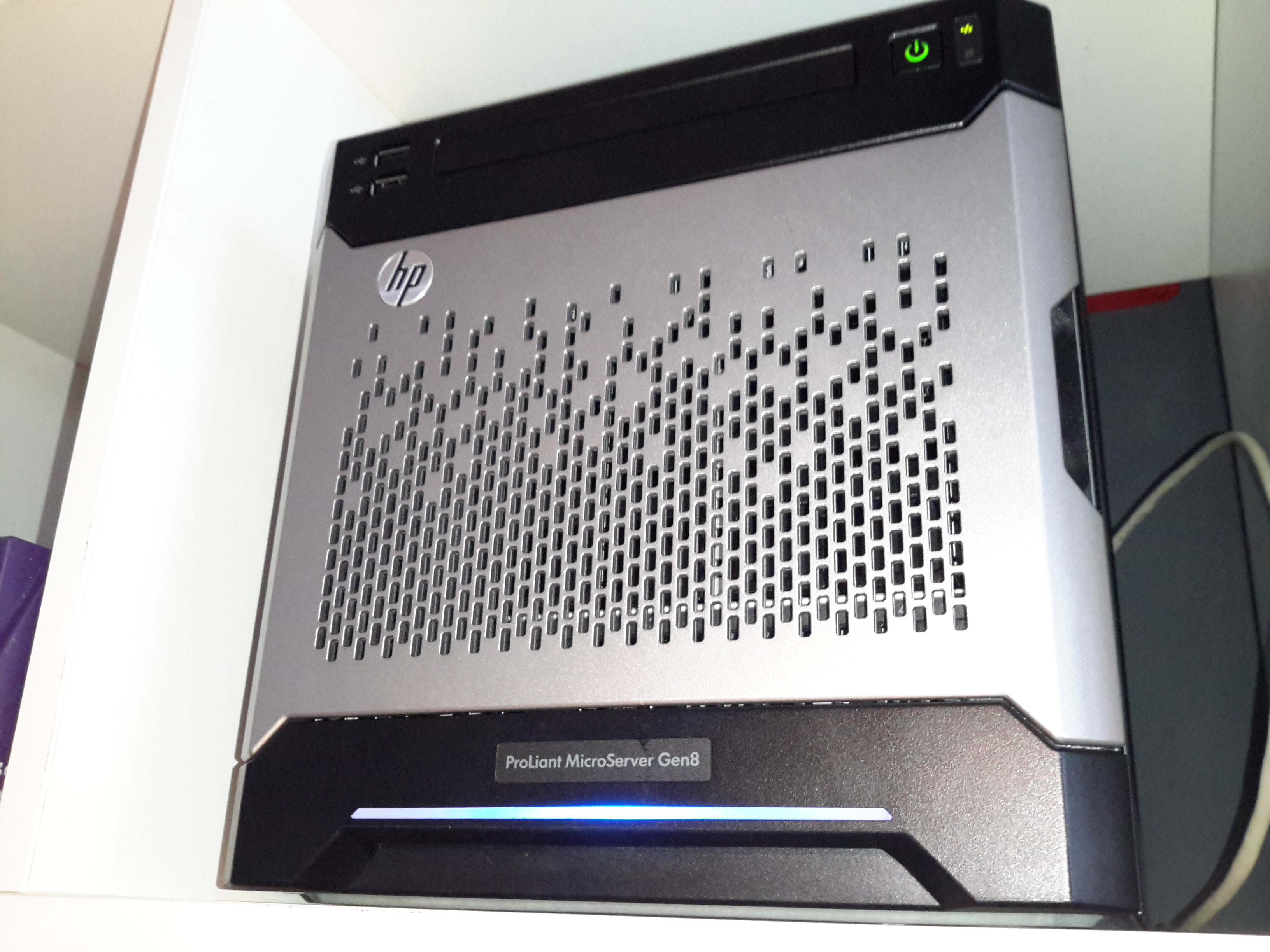
HP Proliant MicroServer Gen 8
This is a Gen 8 HP Proliant Microserver, very small & quiet, perfect for the job. This came with 4GB of RAM installed from the factory, and a Celeron G1610T running at 2.3GHz. Both are a little limited, so some upgrades will be made to the system.
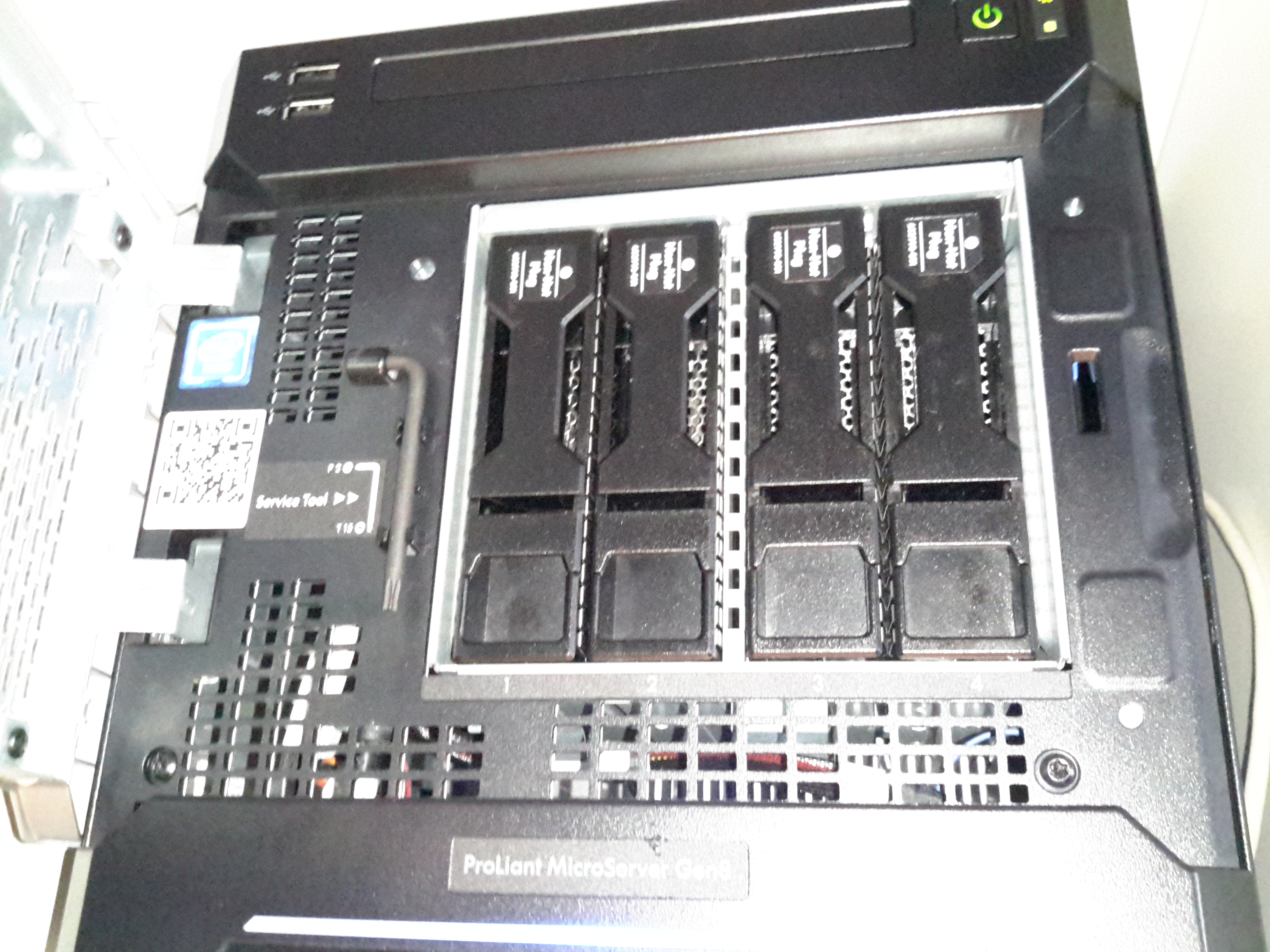
Disk Bays
4 SATA drive bays are located behind the magnetically-locked front door, there’s a 250GB boot disk in here along with a pair of 500GB disks in RAID1 to handle the website files & databases. For my online file hosting site, the server has a backend NFS link direct to Volantis – my 28TB storage server. This arrangement keeps the large file storage side of things off the web server disks & on a NAS, where it should be.
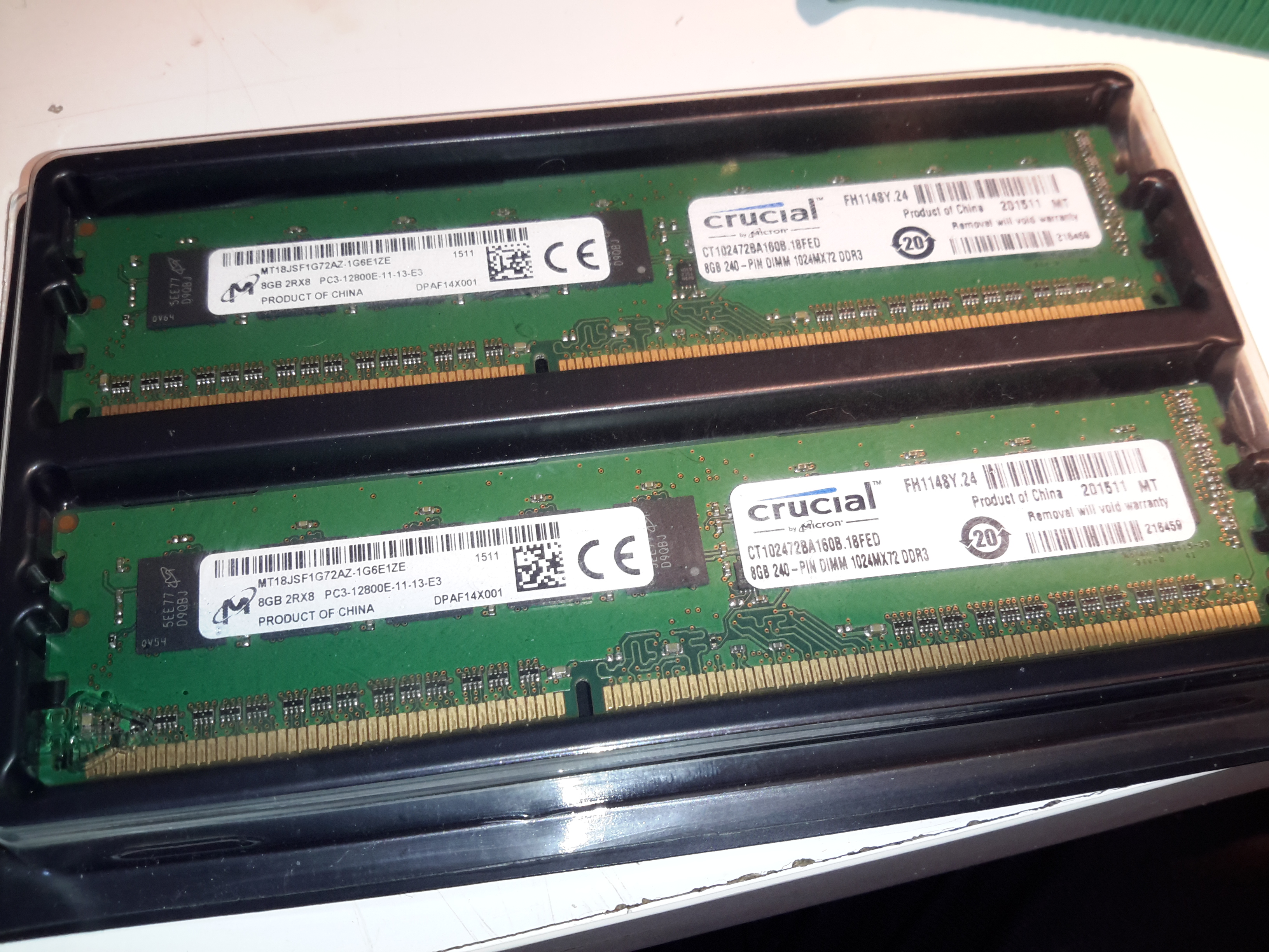
Extra RAM
First thing is a RAM upgrade to the full supported capacity of 16GB. This being a Proliant server machine, doesn’t take anything of a standard flavour, it’s requirements are DDR3-10600E or DDR3-12800E (the E in here being ECC). This memory is both eye-wateringly expensive & difficult to find anywhere in stock. It’s much cheaper & easier to find the ECC Registered variety, but alas this isn’t compatible.
Over the past 48 hours or so, I’ve been migrating everything over to the new baby server, with a couple of associated teething problems, but everything seems to have gone well so far. The remaining job to get everything running as it should is an external mail relay – sending any kind of email from a dynamic IP / domestic ISP usually gets it spam binned by the big providers instantly, regardless of it actually being spam or not – more to come on that setup & configuring postfix to use an external SMTP relay server soon!
If anyone does find something weird going on with the blog, do let me know via the contact page or comments!
I recently got the latest upgrade from Virgin Media, 200Mbit DL / 20Mbit UL, and to get this I was informed I’d have to buy their latest hardware, since my existing CPE wouldn’t be able to handle the extra 5Mbit/s upload speed. (My bullshit detector went off pretty hard at that point, as the SuperHub 2 hardware is definitely capable of working fine with 20Mbit/s upload rates). Instead of having to return the old router, I was asked to simply recycle it, so of course the recycling gets done in my pretty unique way!
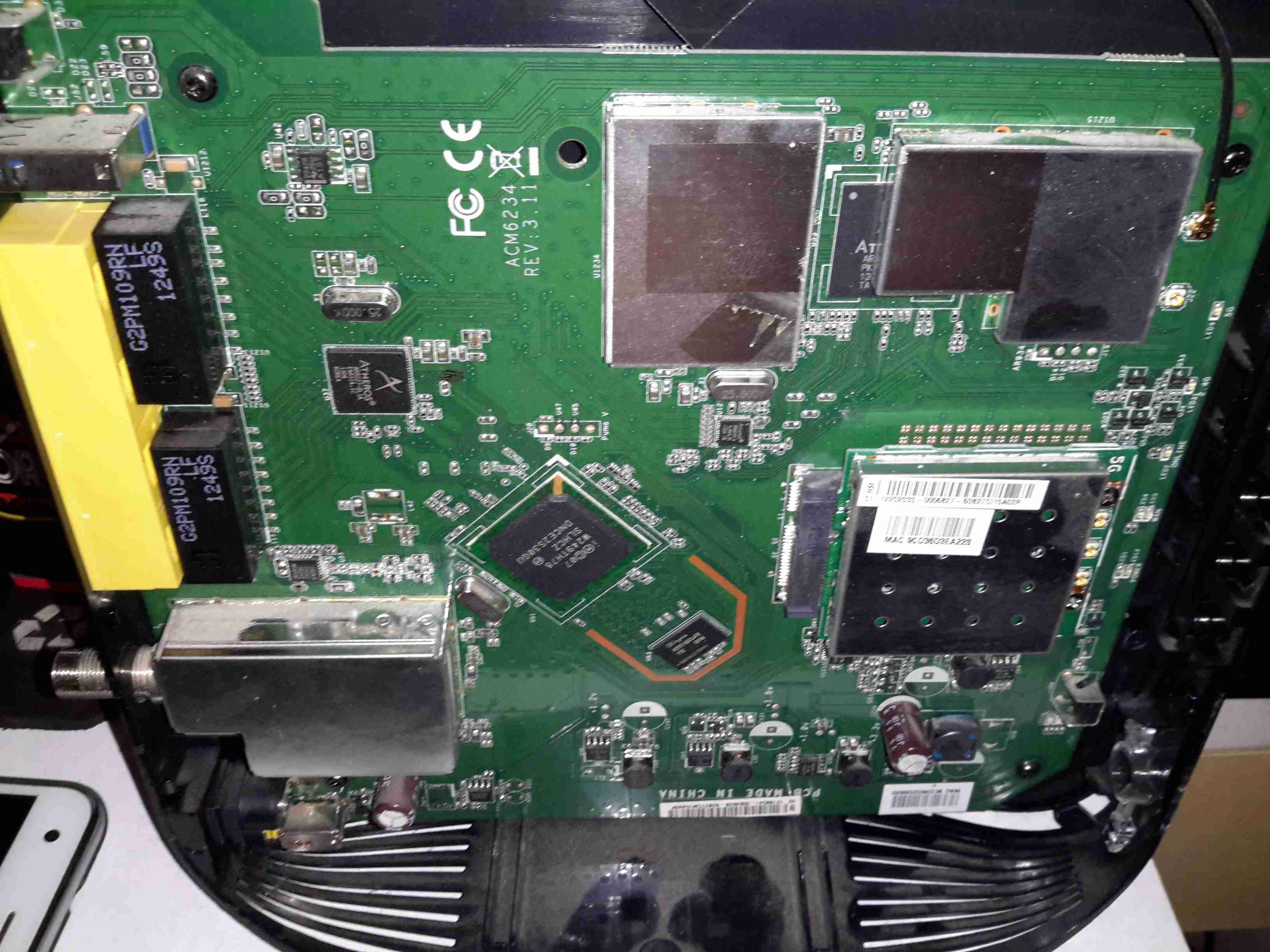
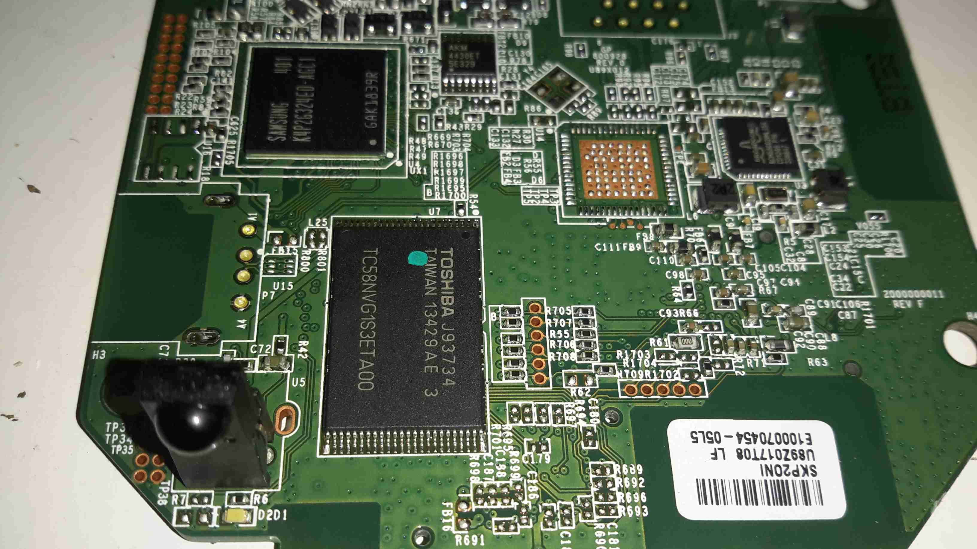
Mainboard
The casing of these units is held together by a single screw & a metric fuckton of plastic clips, disassembly is somewhat hindered by the radio antennas being positioned all over both sides of the casing. Once the side is off, the mainboard is visible. The DOCSIS frontend is lower left, centre is the Intel PUMA 5 Cable Modem SoC with it’s RAM just to the lower right. The right side of the board is taken up by both of the WiFi radio frontends, the 5GHz band being covered by a Mini PCIe card.
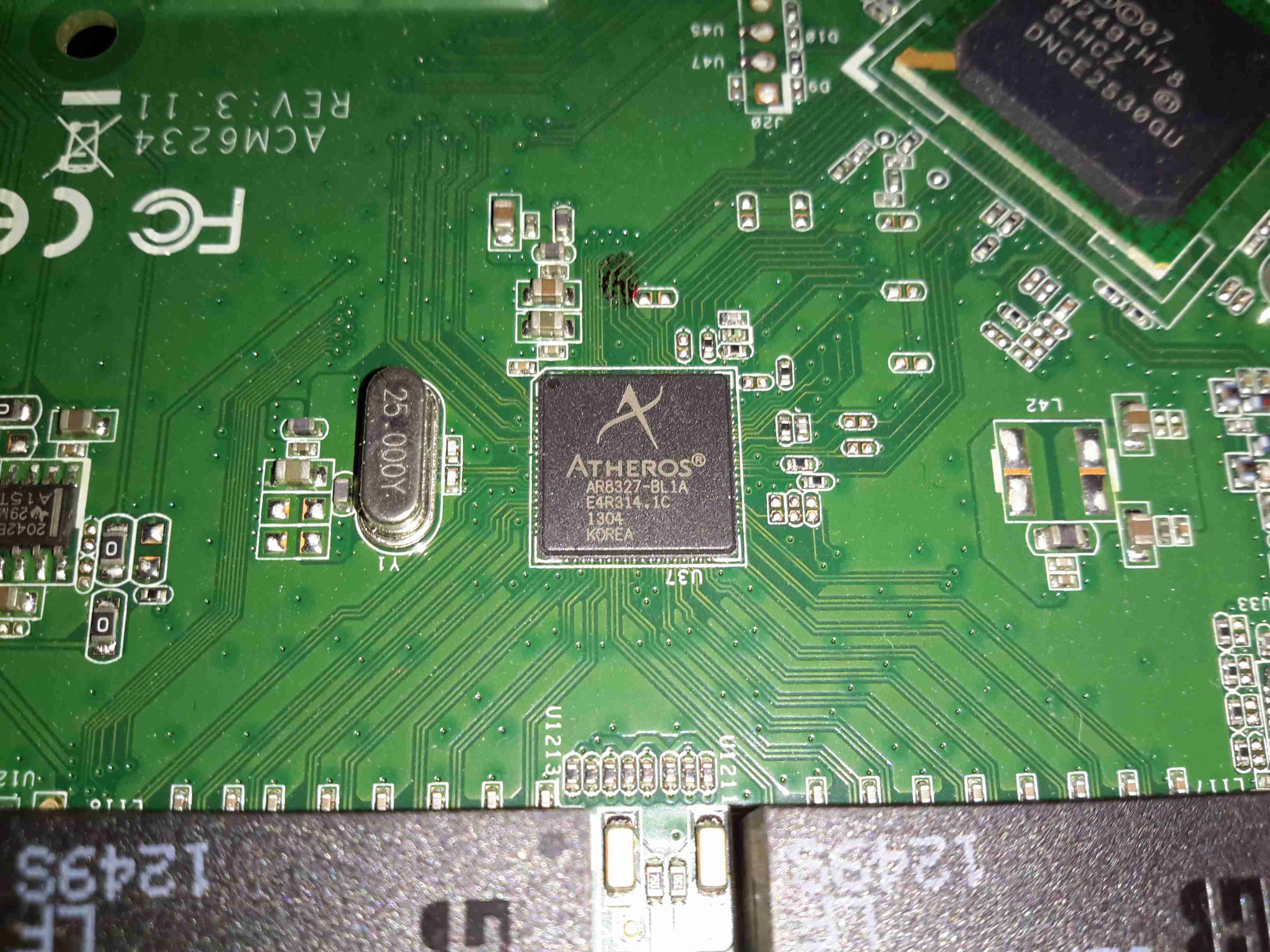
Atheros Gigabit Switch
The 4 gigabit Ethernet ports on the back are serviced by an Atheros AR8327 Managed Layer 3 switch IC, which seems to be a pretty powerful device:
The AR8327 is the latest in high performance small network switching. It is ultra low power, has extensive routing and data management functions and includes hardware NAT functionality (AR8327N). The AR8327/AR8327N is a highly integrated seven-port Gigabit Ethernet switch with a fully non-blocking switch fabric, a high-performance lookup unit supporting 2048 MAC addresses, and a four-traffic class Quality of Service (QoS) engine. The AR8327 has the flexibility to support various networking applications. The AR8327/AR8327N is designed for cost-sensitive switch applications in wireless AP routers, home gateways, and xDSL/cable modem platforms.
Unfortunately most of the features of this router are locked out by VM’s extremely restrictive firmware. With any of their devices, sticking the VM supplied unit into modem mode & using a proper router after is definitely advised!
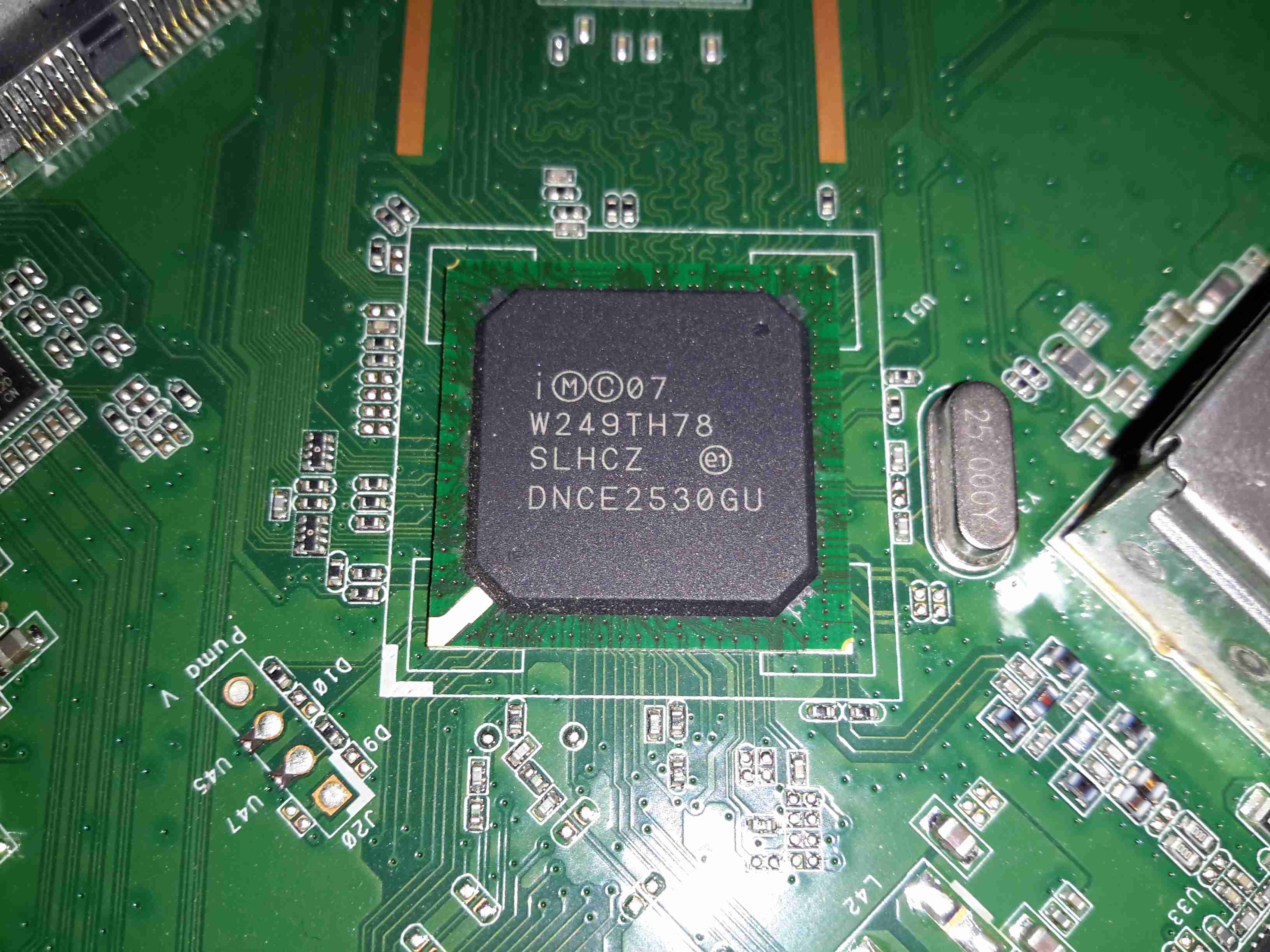
Intel Puma 5 CM CPU
The cable modem side of things is taken care of by the Intel PUMA 5 DNCE2530GU SoC. This appears to communicate with the rest of the system via the Ethernet switch & PCI Express for the 5GHz radio.
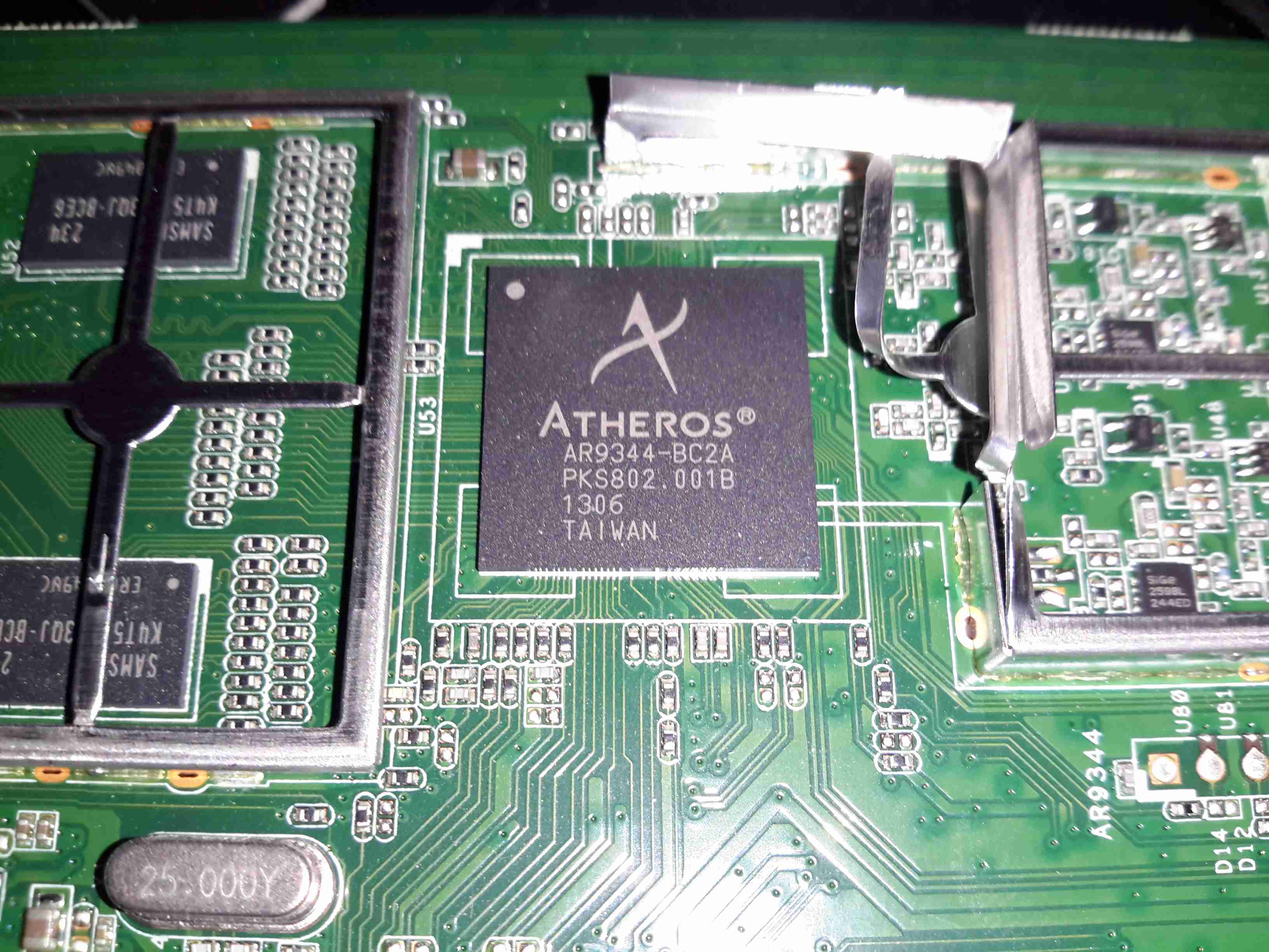
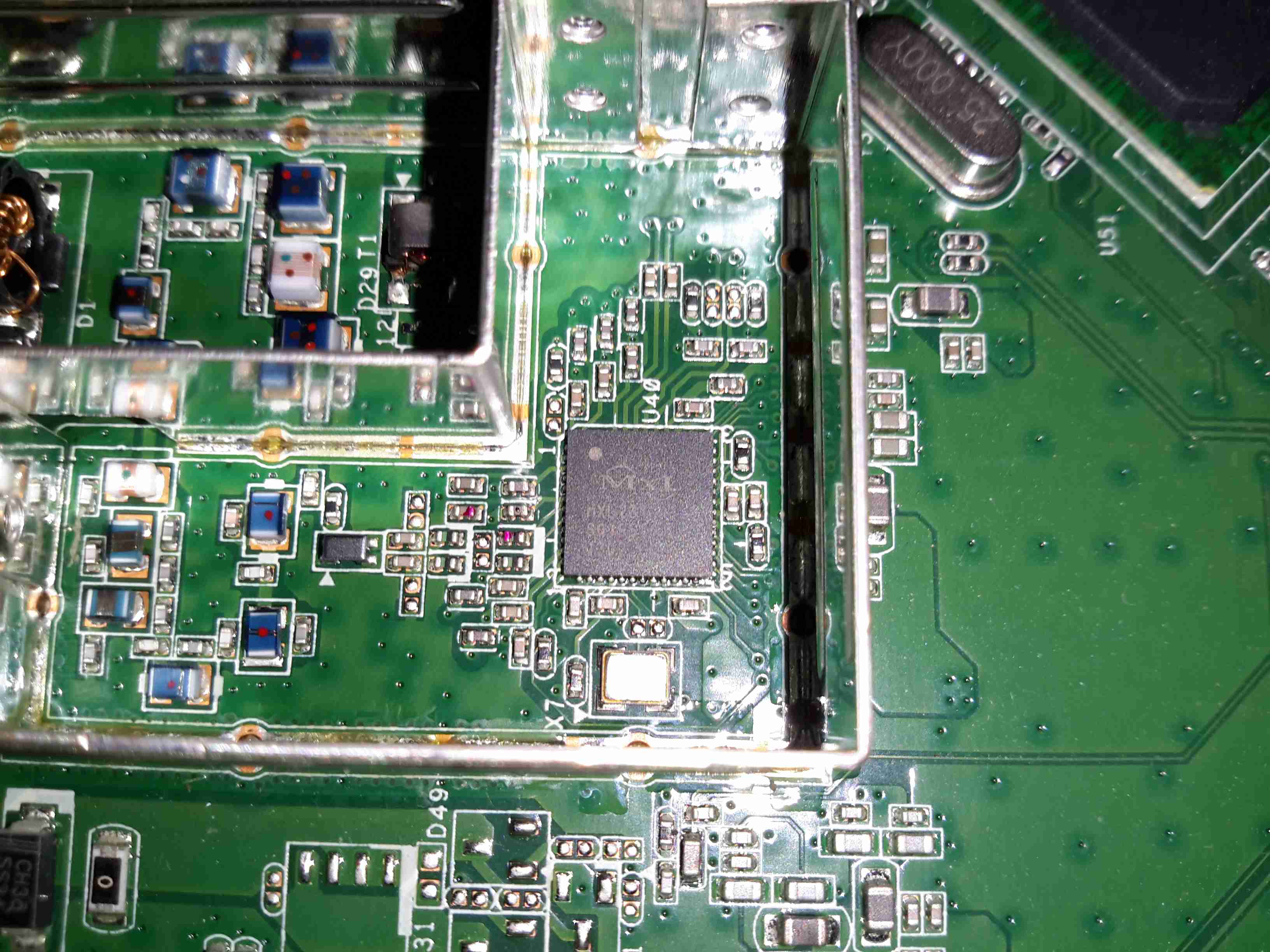
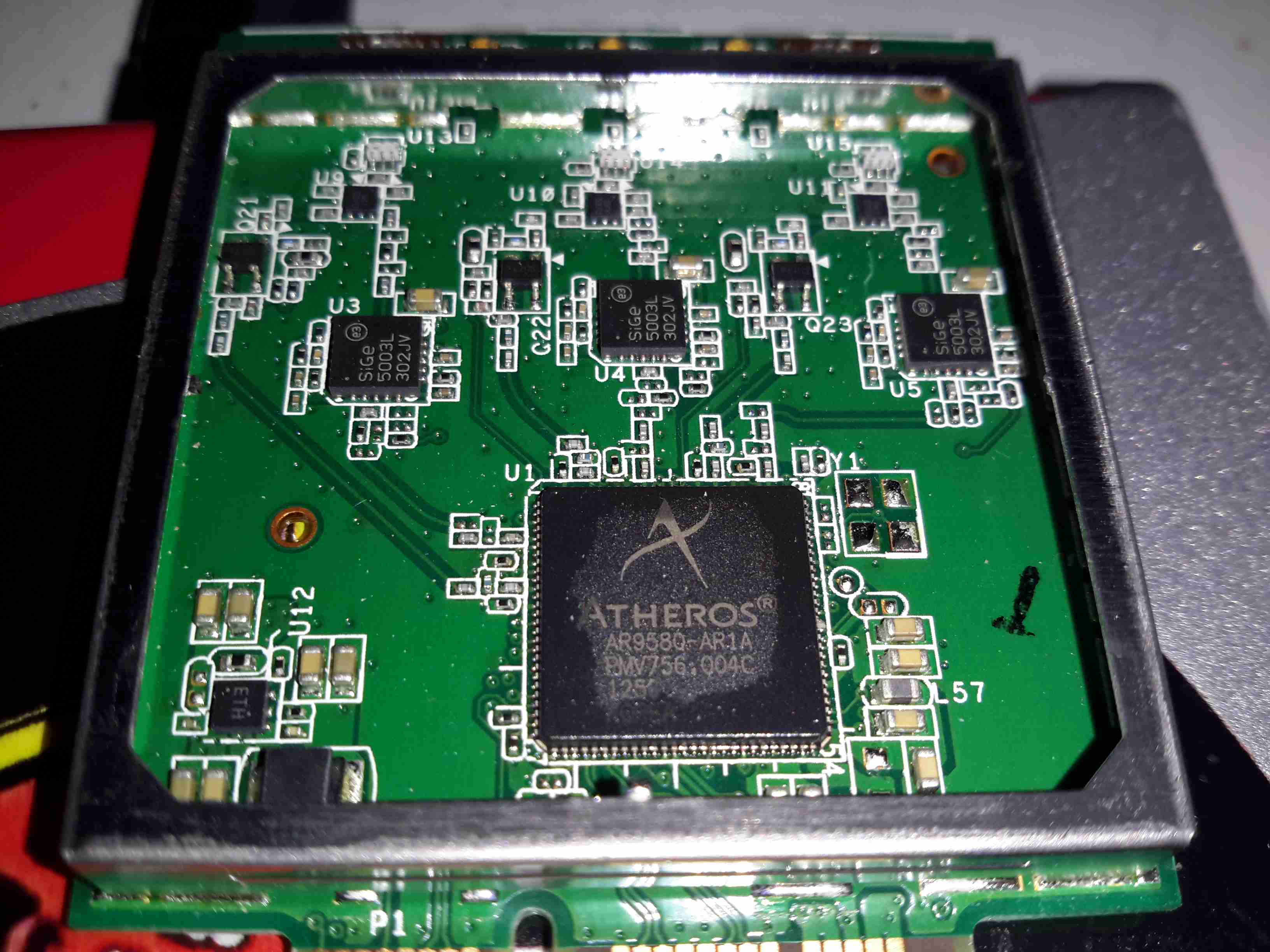
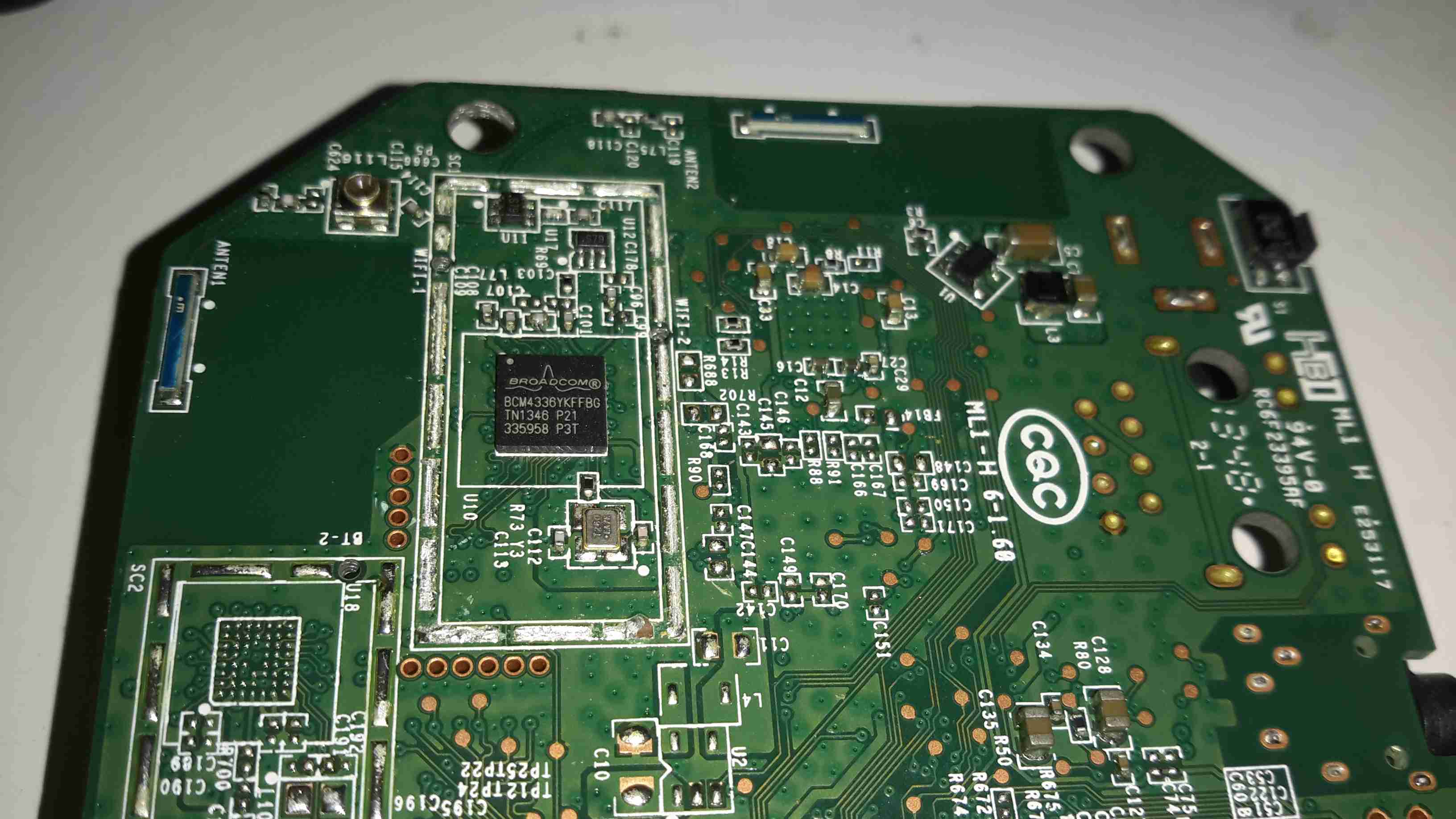
Atheros WiFi SoC
The 2.4GHz radio functionality is supplied by an Atheros AR9344 SoC, it’s RAM is to the left. This is probably handling all the router functions of this unit, but I can’t be certain.
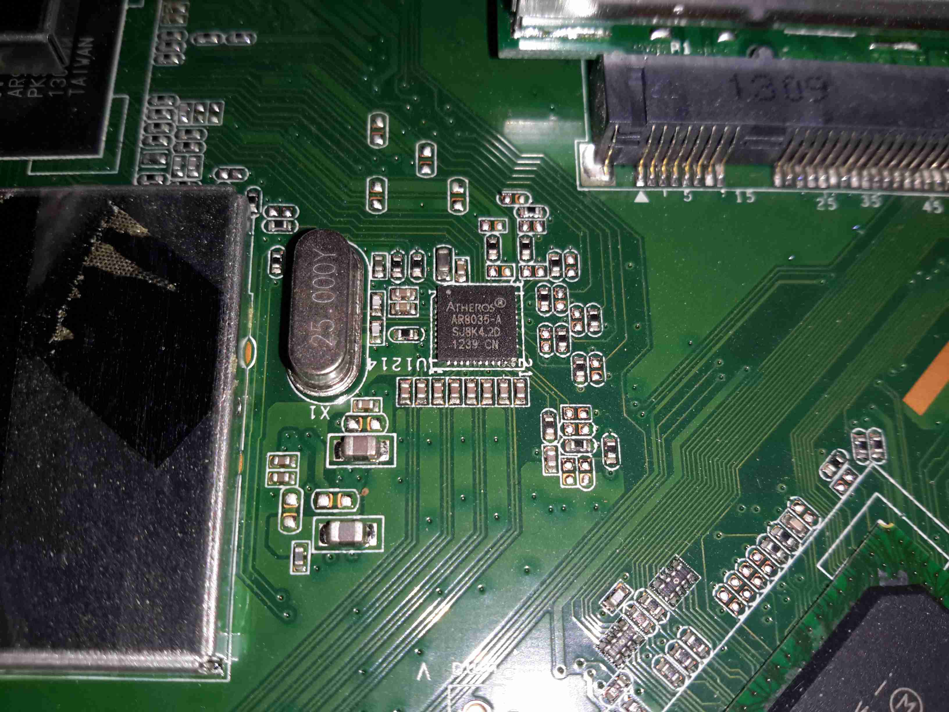
Atheros LAN PHY
A separate Ethernet PHY is located between the SoC & the switch IC.
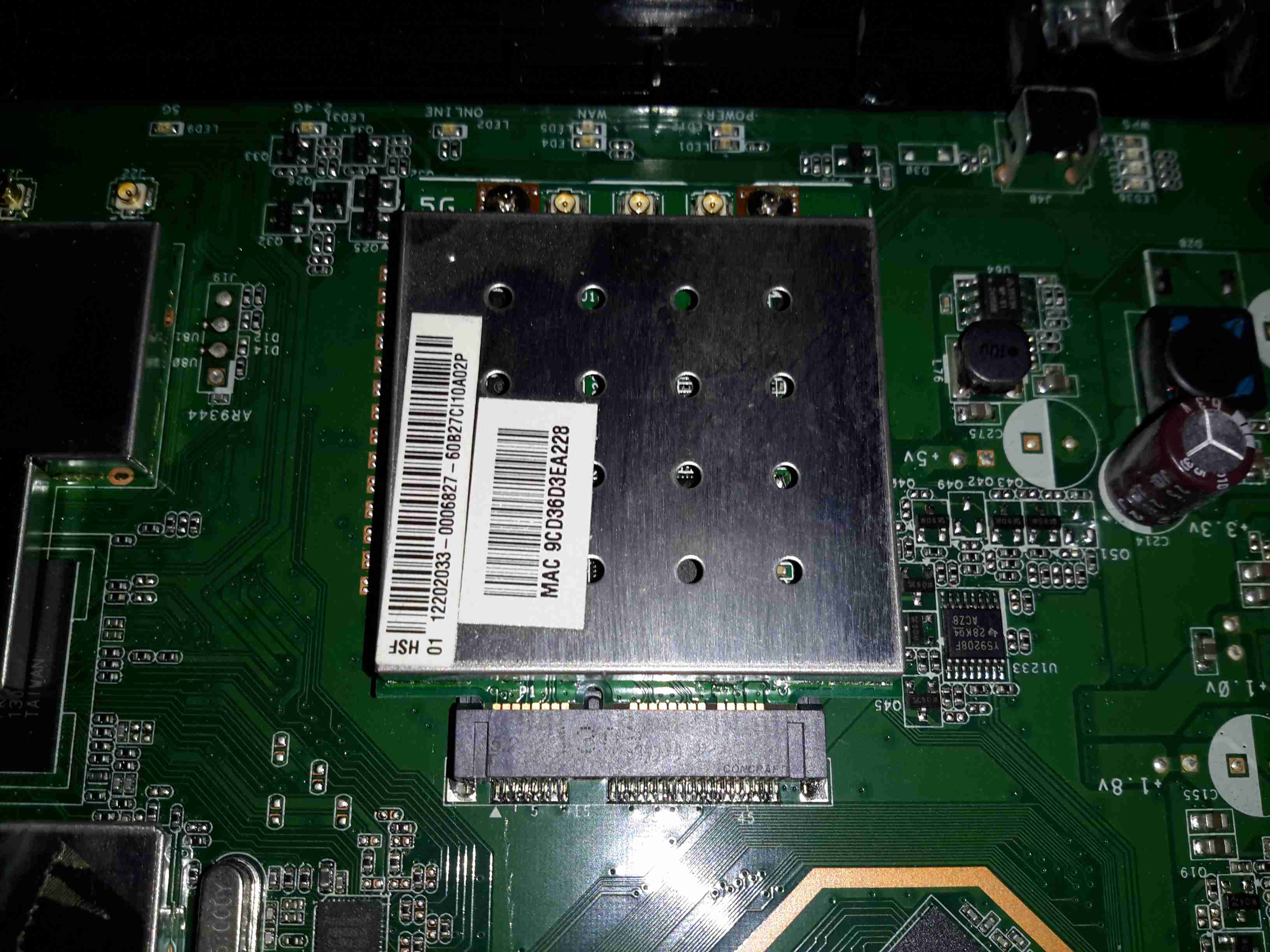
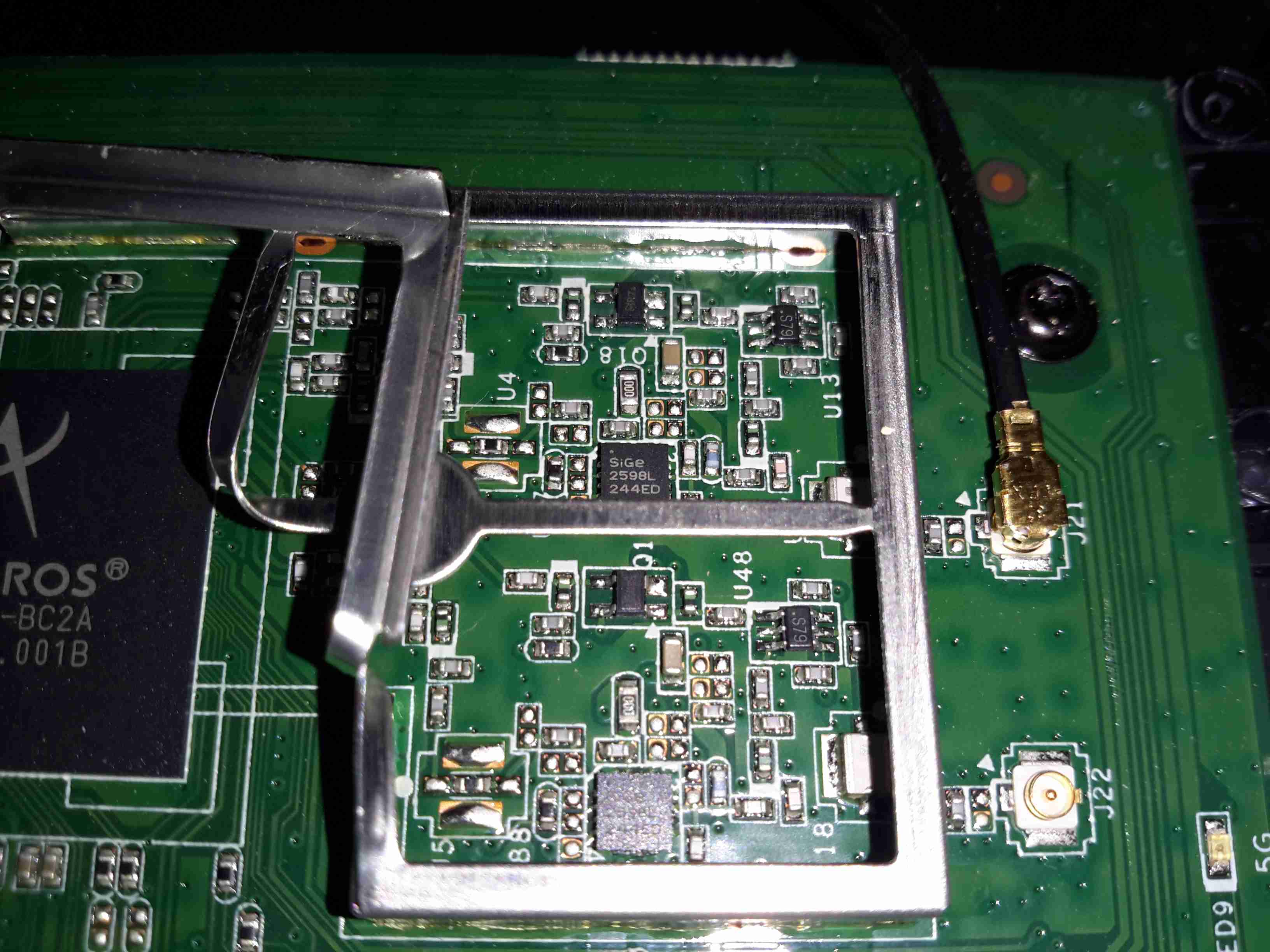
5GHz Radio Card
The 5GHz band is served by a totally separate radio module, in Mini PCIe format, although it’s a bit wider than standard. This module will probably be kept for reuse in another application.
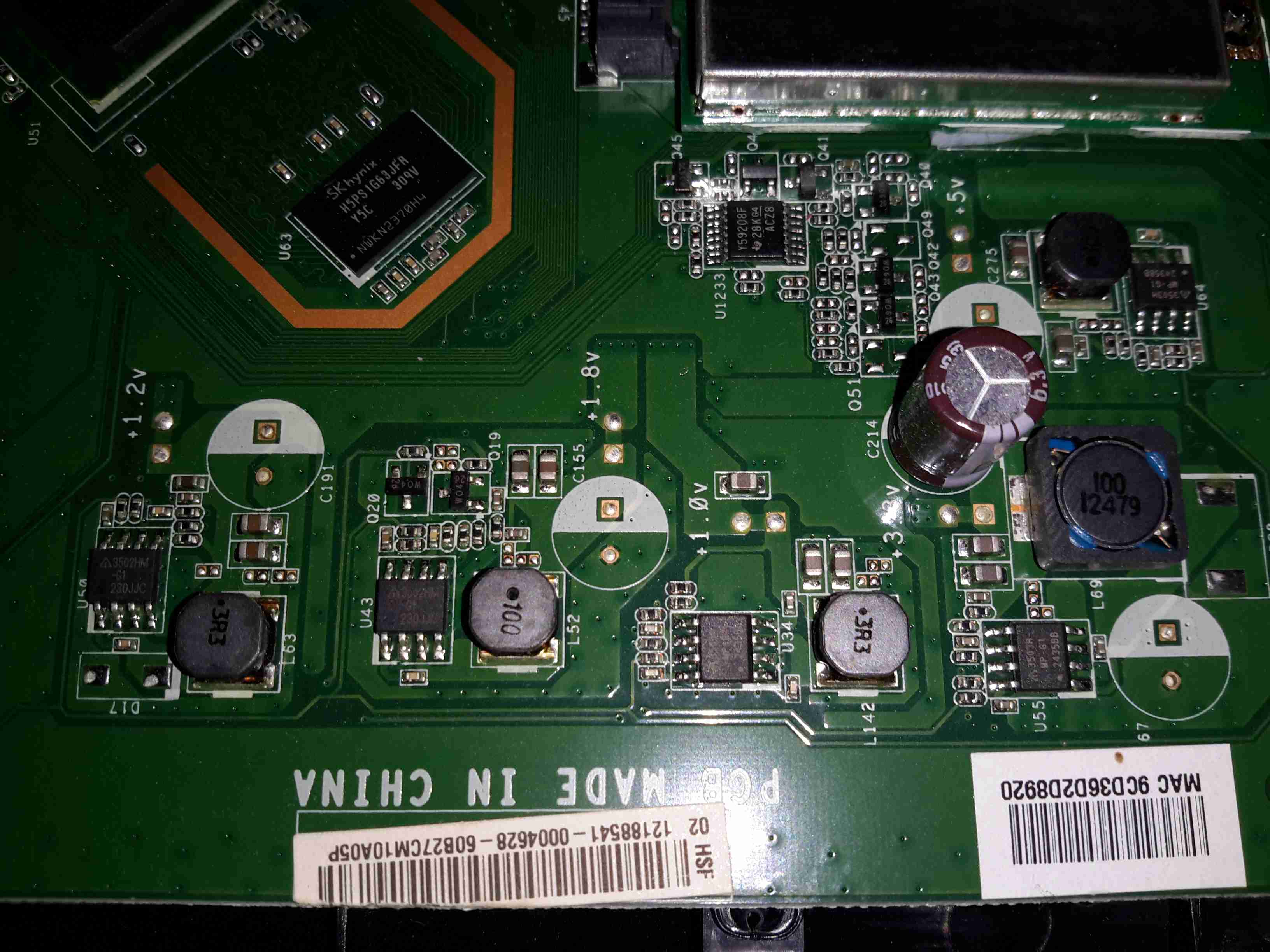
Power Supplies
All down the edge of the board are the multiple DC-DC converters to generate the required voltage rails.
MaxLinear MXL261 Frontend
The DOCSIS frontend is handled by a MaxLinar MXL261 Tuner/Demodulator. More on this IC in my decapping post 🙂
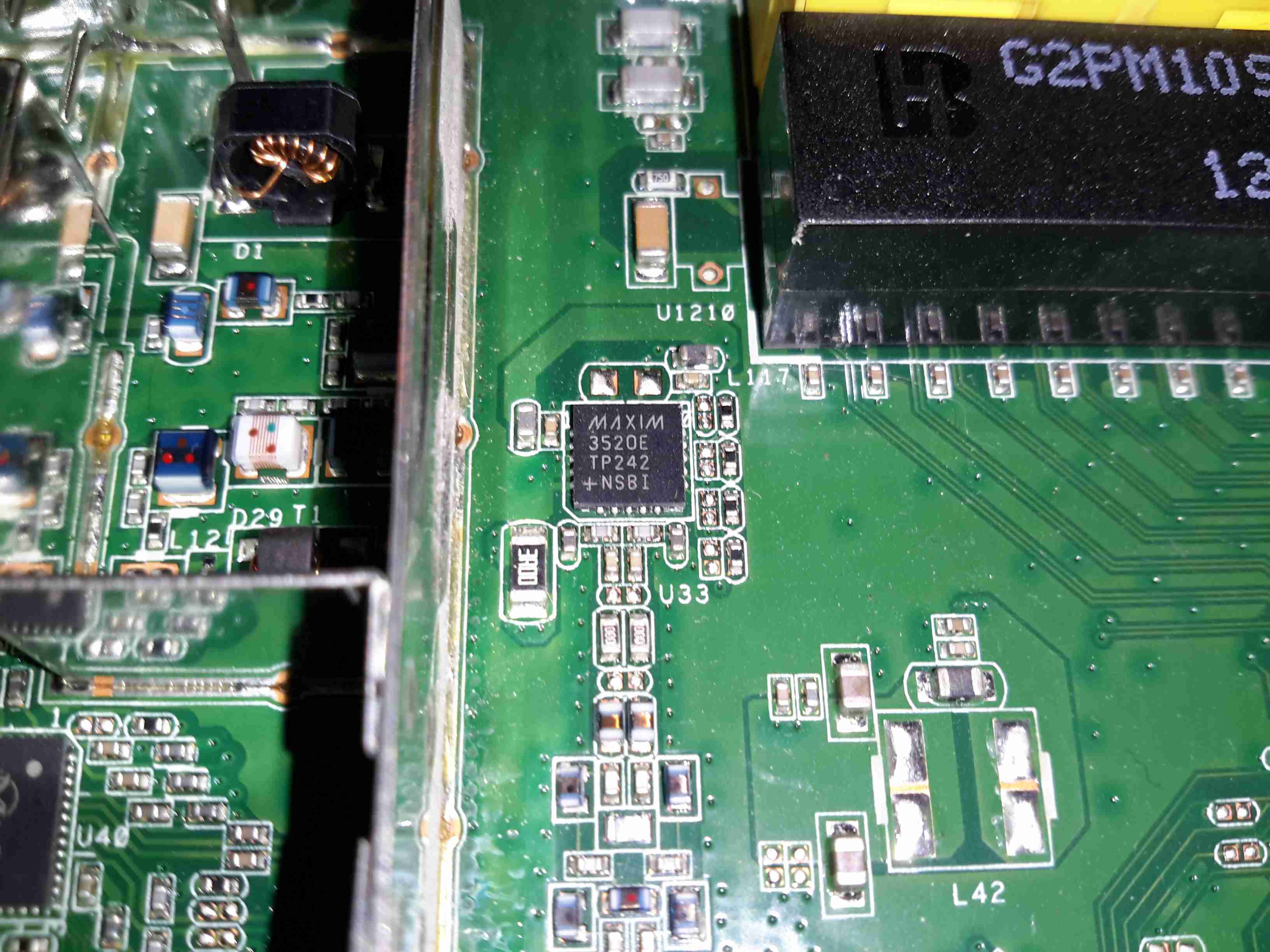
The Unknown One
I’ve honestly no idea what on earth this Maxim component is doing. It’s clearly connected via an impedance matched pair, and that track above the IC looks like an antenna, but nothing I search for brings up a workable part number.
2.4GHz Frontend
The RF switching & TX amplifiers are under a shield, these PA chips are SiGe parts.
Atheros 5GHz Radio
Pretty much the same for the 5GHz radio, but with 3 radio channels.
I was recently given this unit, along with another Behringer sound processor to repair, as the units were both displaying booting problems. This first one is a rather swish Mastering Processor, which has many features I’ll leave to Behringer to explain 😉
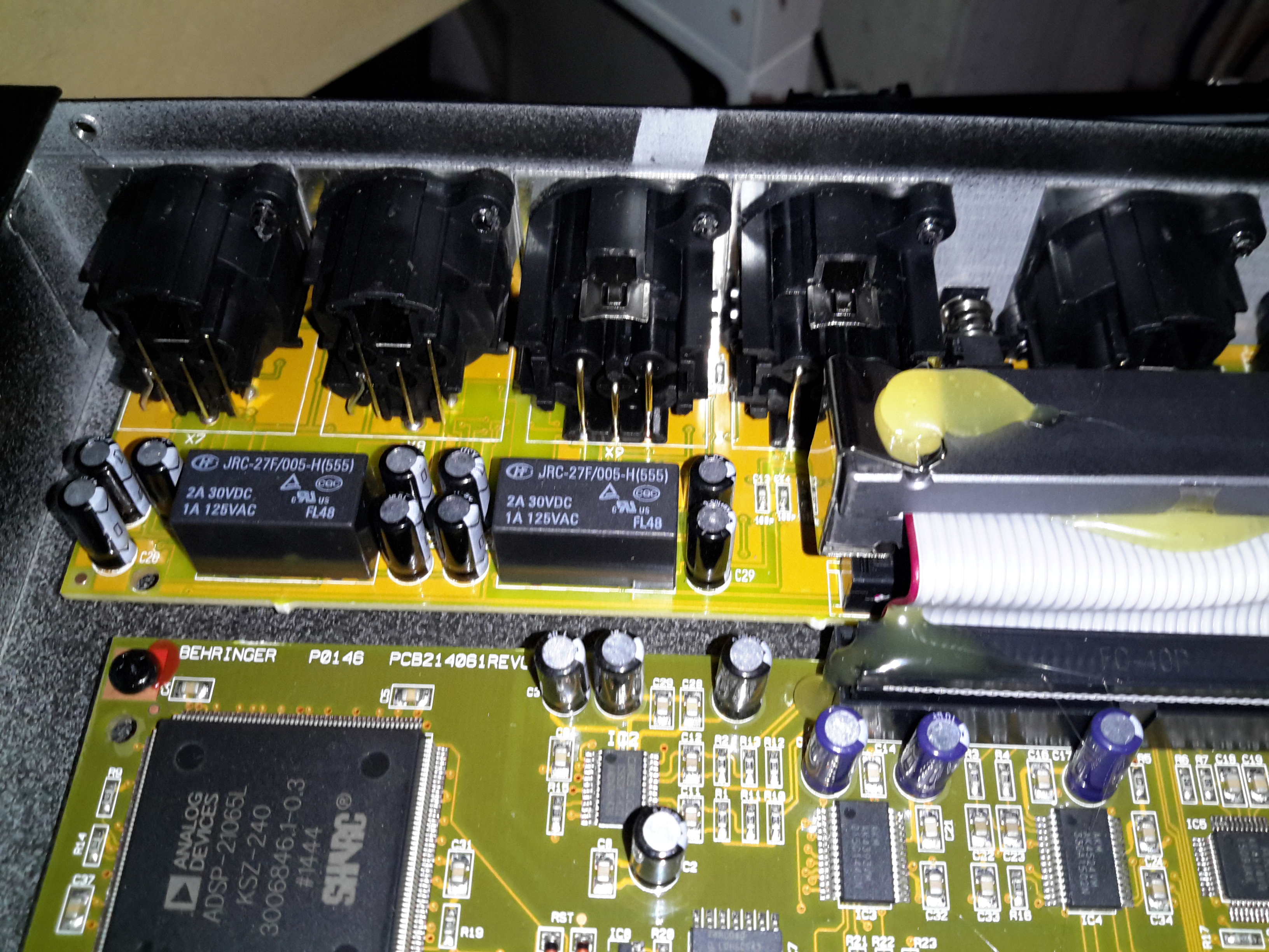
Input Board & Relays
All the inputs are on the back of this 19″ rackmount bit of kit, nothing much on this PCB other than the connectors & a couple of switching relays.
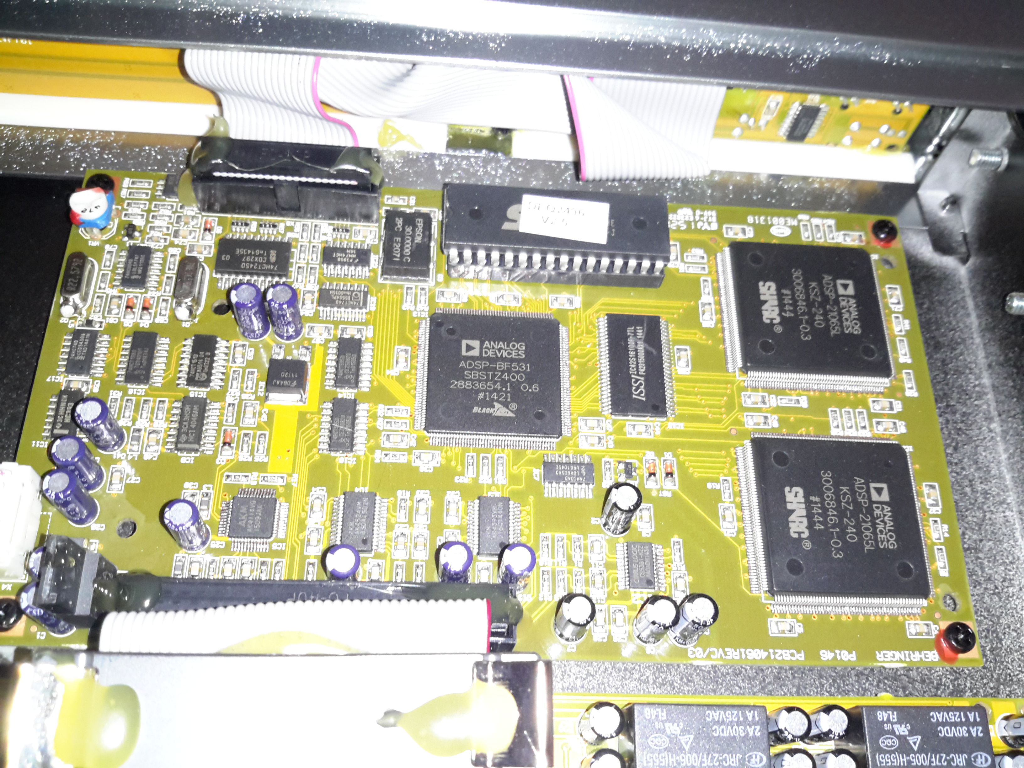
Main Processor PCB
All the magic is done on the main processor PCB, which is host to 3 Analog Devices DSP processors:
ADSP-BF531 BlackFin DSP. This one is probably handling most of the audio processing, as it’s the most powerful DSP onboard at 600Mhz. There’s a ROM on board above this for the firmware & a single RAM chip. On the right are a pair of ADSP-21065 DSP processors at a lower clock rate of 66MHz. To the left is some glue logic to interface the user controls & dot-matrix LCD.
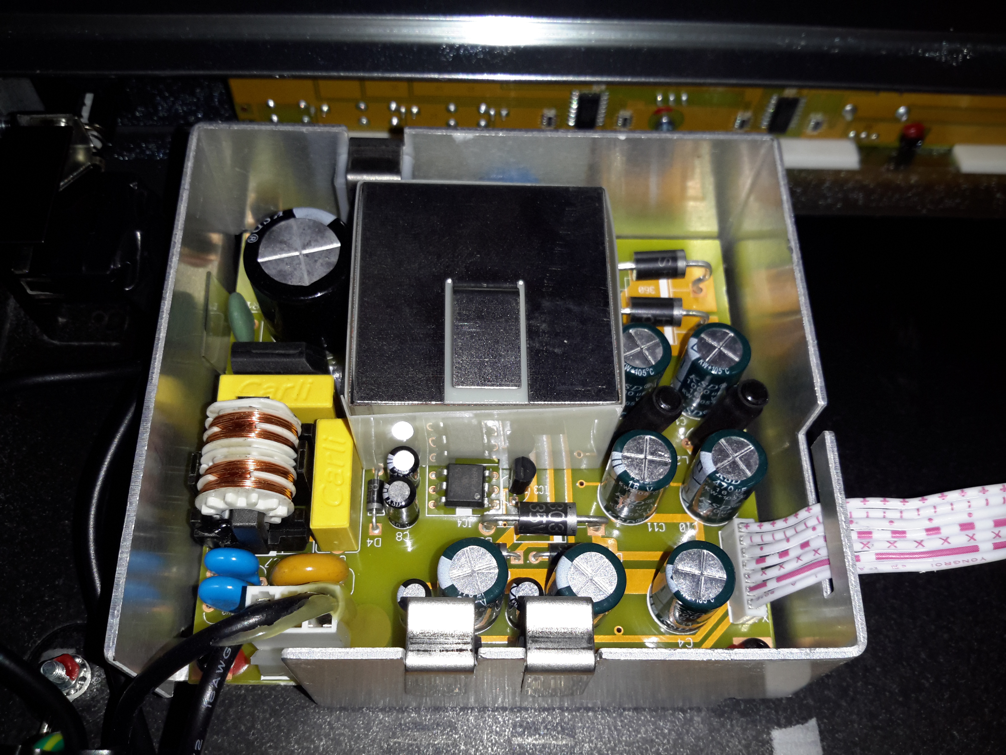
PSU Module
The PSU in this unit is a pretty standard looking SMPS, with some extra noise filtering & shielding. The main transformer is underneath the mu-metal shield in the centre of the board.
Here’s another retired piece of tech that we used to route media from the NAS to the main TV. It was retired since it’s inability to support XBMC/Kodi & having some crashing issues.
Main PCB
After attacking the case with the screwdriver (Torx in this case), the main board comes out. The CPU in this looks *very* familiar, being a PoP device. There are unpopulated places for an ethernet interface & USB port here.
Flash & CPU
After a little digging is turns out the CPU in this device is a BCM2835, with 256MB of RAM stacked on top. It’s a Raspberry Pi! Even the unpopulated part for Ethernet is the same SMSC LAN9512!
There’s 32MB of Flash for the software below the CPU.
On the far right of the board is a Broadcom BCM59002IML Mobile Power Management IC.
WiFi Chipset
On the bottom of the PCB is the WiFi chipset, a Broadcom BCM4336, this most likely communicates with the CPU via SDIO. There’s also a section below for a Bluetooth chipset.
This is the teardown of a Zebra P330i plastic card printer, used for creating ID cards, membership cards, employee cards, etc. I got this as a faulty unit, which I will detail later on.
This printer supports printing on plastic cards from 1-30mils thick, using dye sublimation & thermal transfer type printing methods. Interfaces supplied are USB & Ethernet. The unit also has the capability to be fitted with a mag stripe encoder & a smart card encoder, for extra cost.
Print Engine
On the left here is the print engine open, the blue cartridge on the right is a cleaning unit, using an adhesive roller to remove any dirt from the incoming card stock.
This is extremely important on a dye sublimation based printing engine as any dirt on the cards will cause printing problems.
Cards In Feeder
Here on the right is the card feeder unit, stocked with cards. This can take up to 100 cards from the factory.
The blue lever on the left is used to set the card thickness being used, to prevent misfeeds. There is a rubber gate in the intake port of the printer which is moved by this lever to stop any more than a single card from being fed into the print engine at any one time.
Card Feeder Belt
Here is the empty card feeder, showing the rubber conveyor belt. This unit was in fact the problem with the printer, the drive belt from the DC motor under this unit was stripped, preventing the cards from feeding into the printer.
Print Head
Here is a closeup of the print head assembly. The brown/black stripe along the edge is the row of thin-film heating elements. This is a 300DPI head.
Print Station
This is under the print head, the black roller on the left is the platen roller, which supports the card during printing. The spool in the center of the picture is the supply spool for the dye ribbon.
In the front of the black bar in the bottom center, is a two-colour sensor, used to locate the ribbon at the start of the Yellow panel to begin printing.
LCD PCB
Inside the top cover is the indicator LCD, the back of which is pictured right.
This is a 16×1 character LCD from Hantronix. This unit has a parallel interface.
LCD
Front of the LCD, this is white characters on a blue background.
Roller Drive Belts
Here is the cover removed from the printer, showing the drive belts powering the drive rollers. There is an identical arrangement on the other side of the print engine running the other rollers at the input side of the engine.
Mains Filter
Here the back panel has been removed from the entire print engine, complete with the mains input wiring & RFI filtering.
This unit has excellent build quality, just what is to be expected from a £1,200+ piece of industrial equipment.
Main Frame With Motors
The bottom of the print engine, with all the main wiring & PCB removed, showing the main drive motors. The left hand geared motor operates the head lift, the centre motor is a stepper, which operates the main transmission for the cards. The right motor drives the ribbon take up spindle through an O-Ring belt.
Feeder Drive Motor
Card feeder drive motor, this connects to the belt assembly through a timing belt identical to the roller drive system.
All these DC geared motors are 18v DC, of varying torque ratings.
Power Supply
Here is the main power supply, a universal input switch-mode unit, outputting 24v DC at 3.3A.
PSU Label
PSU info. This is obviously an off the shelf unit, manufactured by Hitek. Model number FUEA240.
Print Engine Rear
The PSU has been removed from the back of the print engine, here is shown the remaining mechanical systems of the printer.
Print Engine Components
A further closeup of the print engine mechanical bay, the main stepper motor is bottom centre, driving the brass flywheel through another timing belt drive. The O-Ring drive on the right is for the ribbon take up reel, with the final motor driving the plastic cam on the left to raise/lower the print head assembly.
The brass disc at the top is connected through a friction clutch to the ribbon supply reel, which provides tension to keep it taut. The slots in the disc are to sense the speed of the ribbon during printing, which allows the printer to tell if there is no ribbon present or if it has broken.
RFID PCB
Here is a further closeup, showing the RFID PCB behind the main transmission. This allows the printer to identify the ribbon fitted as a colour or monochrome.
The antenna is under the brass interrupter disc on the left.
I/O Daughterboard
The I/O daughterboard connects to the main CPU board & interfaces all the motors & sensors in the printer.
Main PCB
Here is the main CPU board, which contains all the logic & processing power in the printer.
CPU
Main CPU. This is a Freescale Semiconductor part, model number MCF5206FT33A, a ColdFire based 32-bit CPU. Also the system ROM & RAM can be seen on the right hand side of this picture.
Ethernet Interface
Bottom of the Ethernet interface card, this clearly has it’s own RAM, ROM & FPGA. This is due to this component being a full Parallel interface print server.
Ethernet Interface Top
Top of the PCB, showing the main processor of the print server. This has a ferrite sheet glued to the top, for interference protection.
A 5 megapixel digital camera from Vivitar. Visible here is the lens, viewfinder & flash.
Back
Rear of the unit showing the LCD & user control buttons.
Cover Removed
Front frame removed showing some of the internals. Shutter assembly & lens in centre, battery compartment at left.
Rear Cover Removed
Rear frame removede, showing the LCD module & tactile switches.
LCD
LCD module removed from the PCB
Flash PCB
Flash PCB removed. Transformer is fed with the 4.5v from the 3 AA cells & steps it up to ~300v DC for the flash capacitor. A pulse transformer energizes an electrode next to the Xenon flash tube with ~5kV to ionize the gas.
Main PCB
Main PCB removed. Internal flash ROM & RAM IC visible above the SD card socket. USB connector is at the top right, next to the piezo buzzer.
CPU
Main processor on reverse side of the PCB.
Image Sensor
Closeup of the CMOS image sensor with the lens assembly removed.
Another phone from the mid 90s. This is the nokia 7110.
Slider Open
Here the slider is open showing the keypad.
Battery Removed
Here the battery is removed, a Li-Ion unit.
Battery
The battery cell & protection circuit removed from the casing.
Rear Of PCB
This is the rear of the PCB removed from the housing. Data & charging ports on the right hand side f the board.
Front Of PCB
Front of the PCB with the RF sections at the left hand side & the keypad contacts on the right.
RF Sections
Closeup of the RF sections of the board, big silver rectangular cans are VCO units.
SIM Connector
Closeup of the top rear section of the PCB, with SIM cnnector, battery contacts, IR tranciever at the far left. Bottom centre is the external antenna connector.
CPU
The logic section of the board, Large chip is CPU, to right of that is the ROM storing the machine code. Other chips are unknown custom parts.
Mic & Speaker
The Mic & the loudspeaker removed from it’s housing.
LCD
LCD from the front of the unit, SPI interfaced. Flex PCB also contains the power button, loudspeaker contacts & a temperature sensor.
Scroll Wheel
The scroll wheel removed from the front housing.
Vibra-Motor
Tiny vibration motor removed from the rear housing, alerts the user to a text or phone call.
Here is a phone from the mid 90s, the Ericsson GA628. Here visible is the front of the unit with keypad, & single line monochrome LCD for number display.
Battery & Rear
Here the battery is removed from the phone, showing the SIM card socket. At the top under the antenna stub is the socket for an external antenna.
Front Removed
Here the front is removed from the phone, PCB on left, rear of keypad on right. Microphone is at bottom of keypad, with speaker at the top. Top right of the PCB is the ringer buzzer, left is shield for RF amplifier.
Main PCB
Here is the back of the main PCB, RF sections on left & centre. Processing & memory on right.
Battery
This phone had a Ni-Mh battery, before Li-Ion batteries were introduced.
LCD
The LCD from the front of the phone is shown here. A simple dot matrix single line unit.
Tip Jar
If you’ve found my content useful, please consider leaving a donation by clicking the Tip Jar below!
All collected funds go towards new content & the costs of keeping the server online.