Posted on 8 Comments

Virgin Media Superhub 2 Teardown

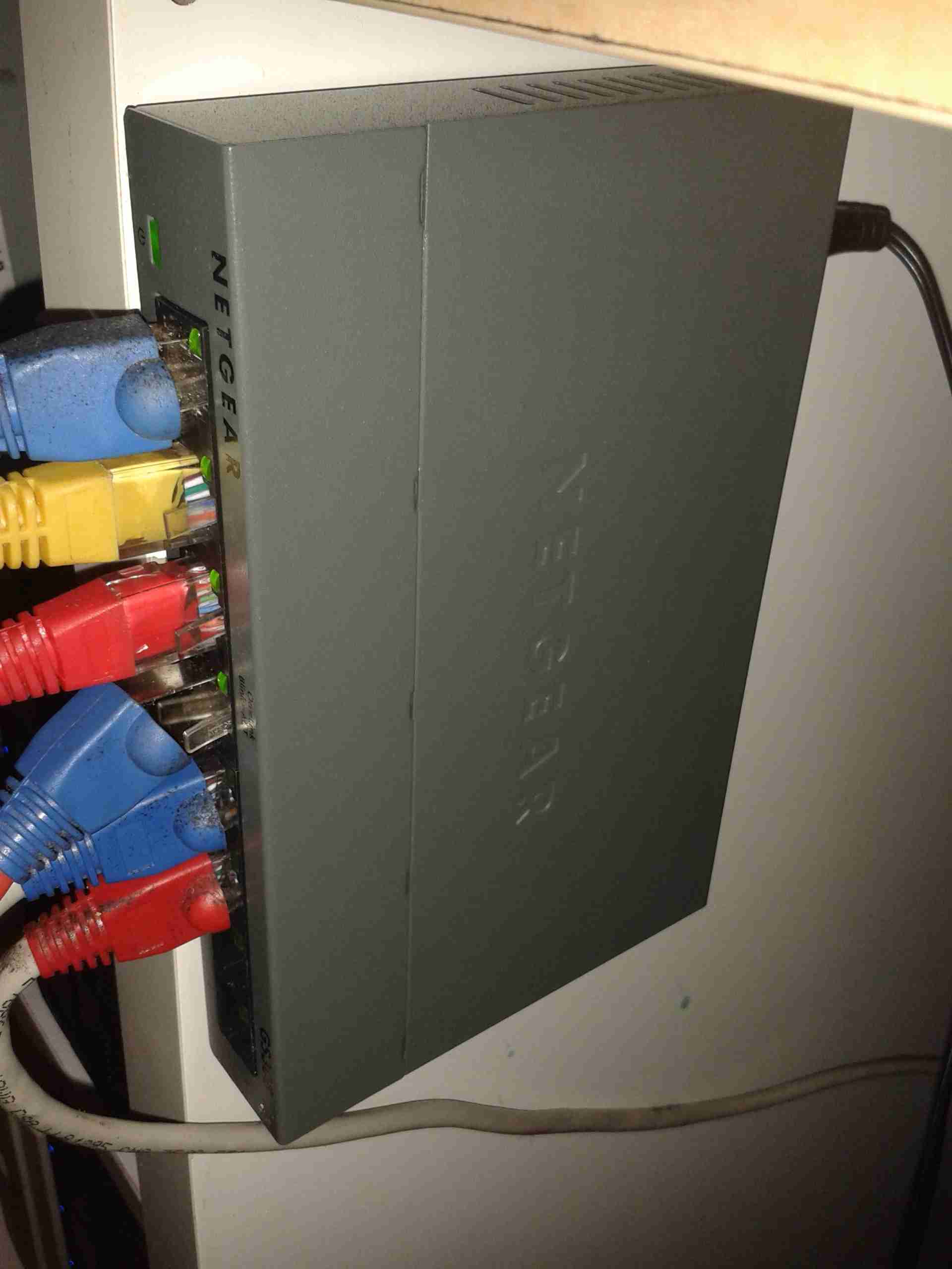
I recently got the latest upgrade from Virgin Media, 200Mbit DL / 20Mbit UL, and to get this I was informed I’d have to buy their latest hardware, since my existing CPE wouldn’t be able to handle the extra 5Mbit/s upload speed. (My bullshit detector went off pretty hard at that point, as the SuperHub 2 hardware is definitely capable of working fine with 20Mbit/s upload rates). Instead of having to return the old router, I was asked to simply recycle it, so of course the recycling gets done in my pretty unique way!

Mainboard
Mainboard

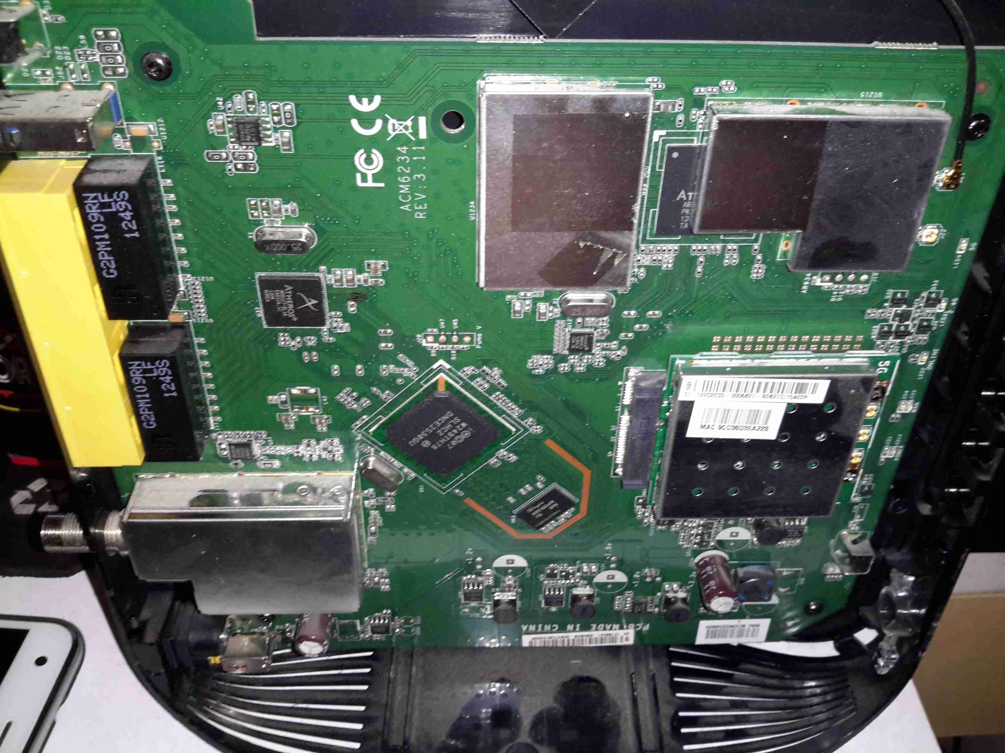
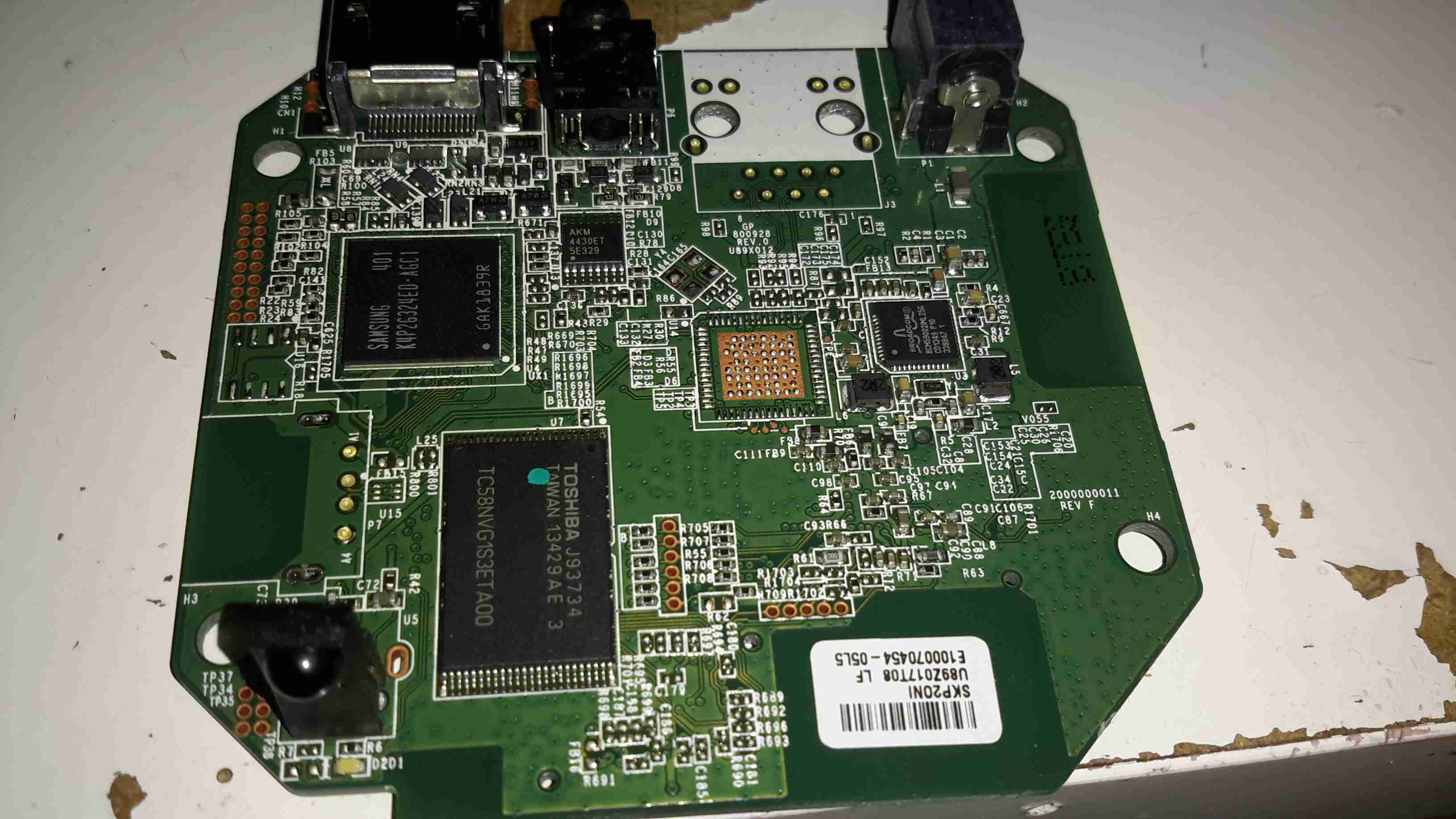
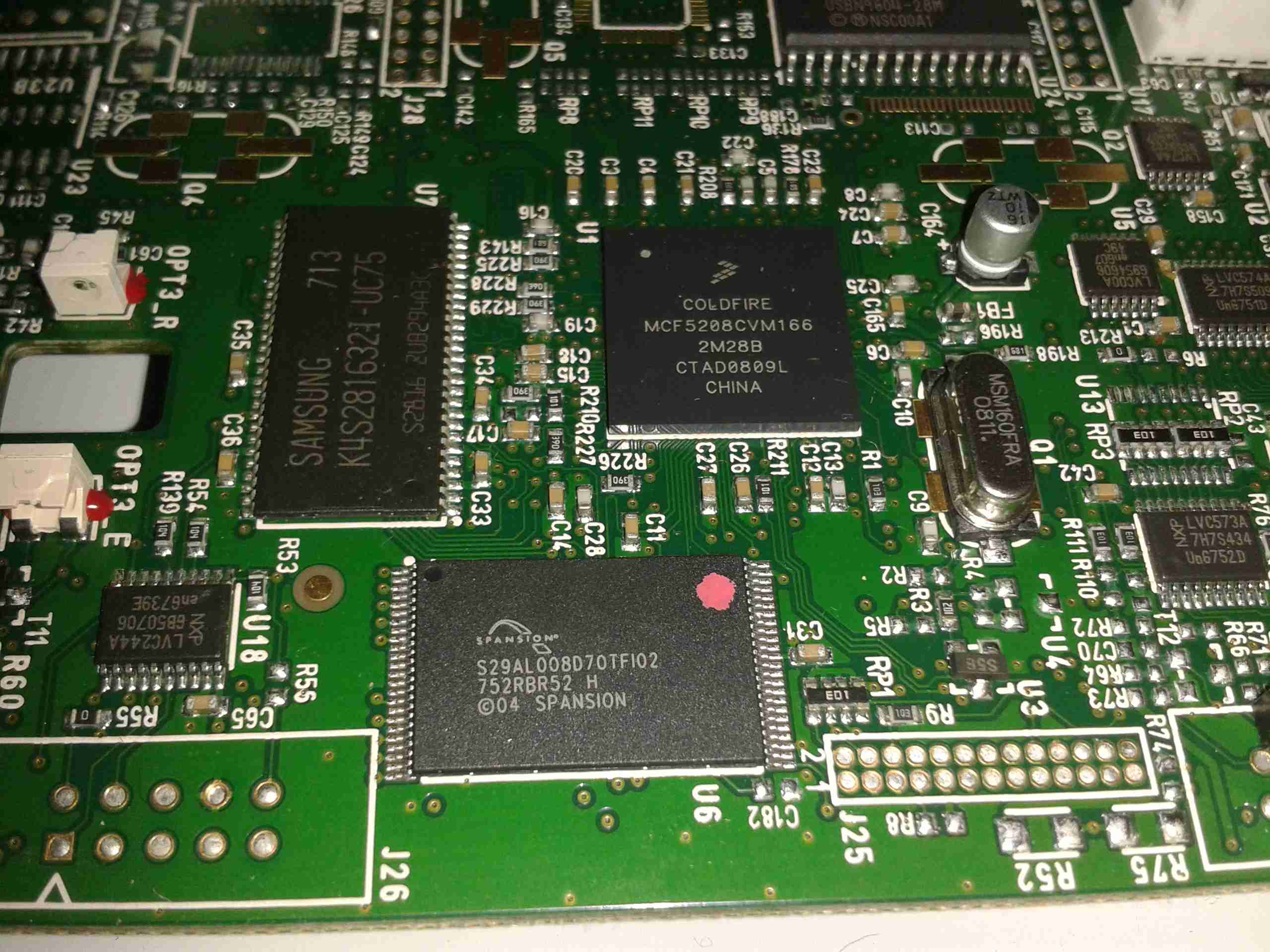
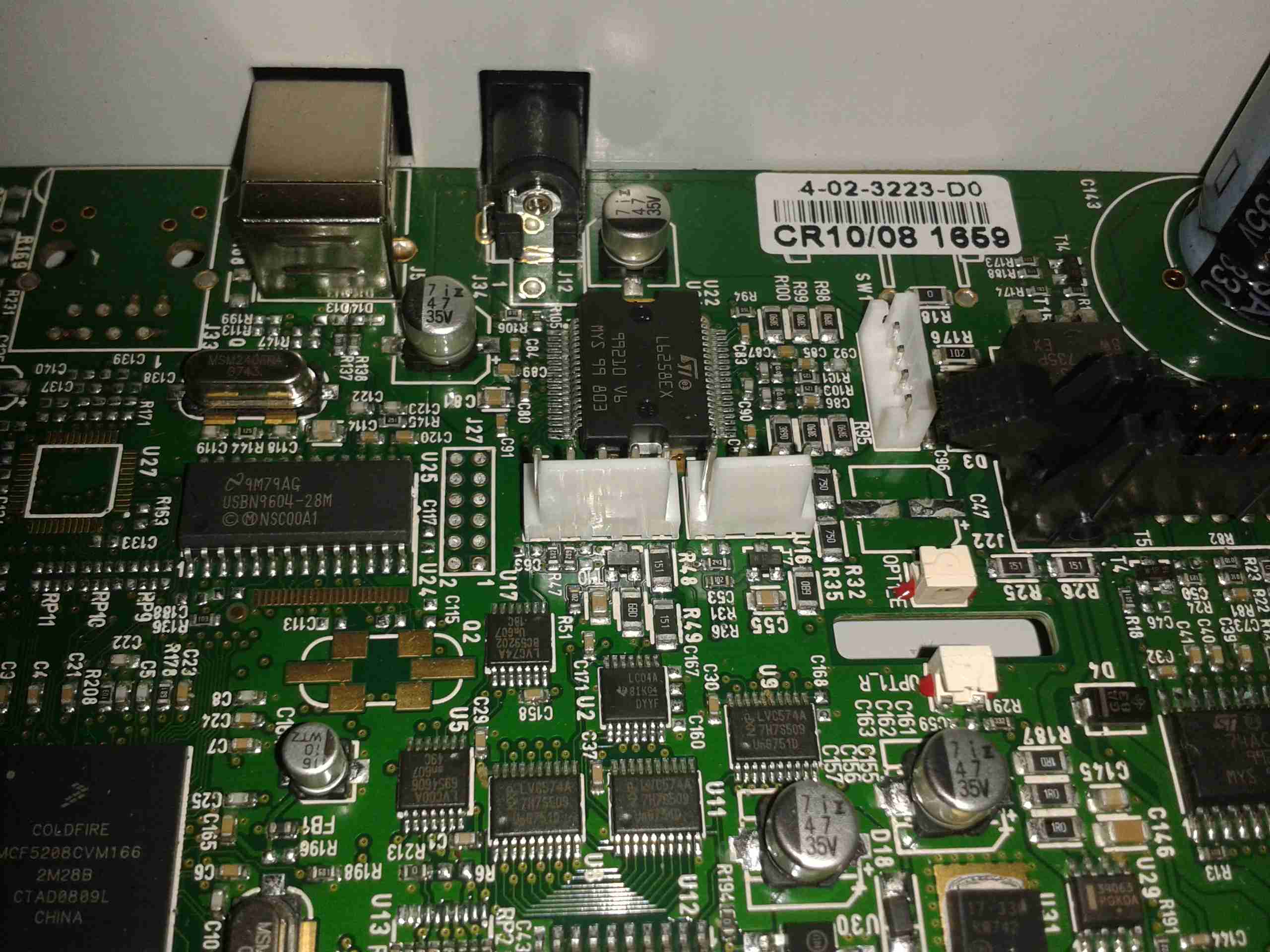
The casing of these units is held together by a single screw & a metric fuckton of plastic clips, disassembly is somewhat hindered by the radio antennas being positioned all over both sides of the casing. Once the side is off, the mainboard is visible. The DOCSIS frontend is lower left, centre is the Intel PUMA 5 Cable Modem SoC with it’s RAM just to the lower right. The right side of the board is taken up by both of the WiFi radio frontends, the 5GHz band being covered by a Mini PCIe card.

Atheros Gigabit Switch

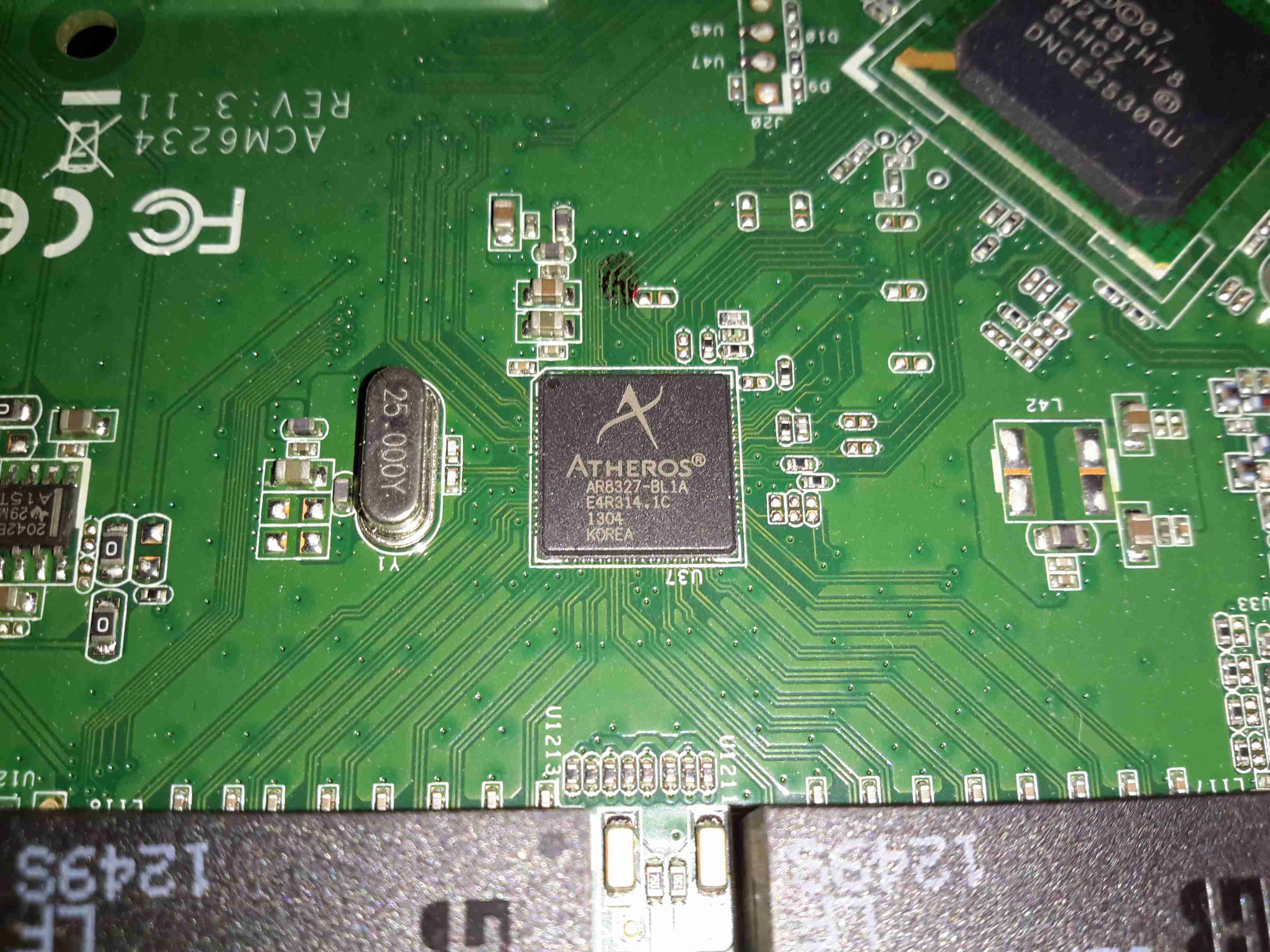
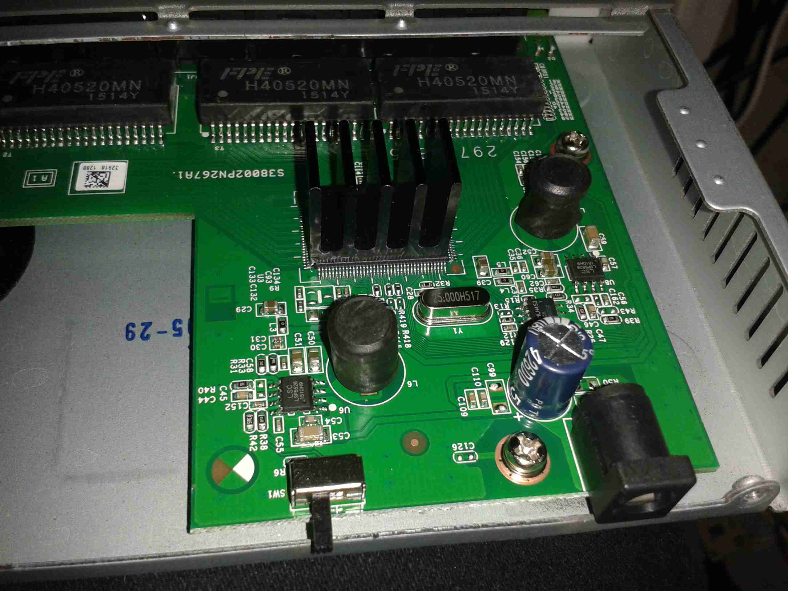
The 4 gigabit Ethernet ports on the back are serviced by an Atheros AR8327 Managed Layer 3 switch IC, which seems to be a pretty powerful device:

The AR8327 is the latest in high performance small network switching. It is ultra low power, has extensive routing and data management functions and includes hardware NAT functionality (AR8327N). The AR8327/AR8327N is a highly integrated seven-port Gigabit Ethernet switch with a fully non-blocking switch fabric, a high-performance lookup unit supporting 2048 MAC addresses, and a four-traffic  class Quality of Service (QoS) engine. The AR8327 has the flexibility to support various networking applications. The AR8327/AR8327N is designed for cost-sensitive switch applications in wireless AP routers, home gateways, and xDSL/cable modem platforms.

Unfortunately most of the features of this router are locked out by VM’s extremely restrictive firmware. With any of their devices, sticking the VM supplied unit into modem mode & using a proper router after is definitely advised!

Intel Puma 5 CM CPU
Intel Puma 5 CM CPU

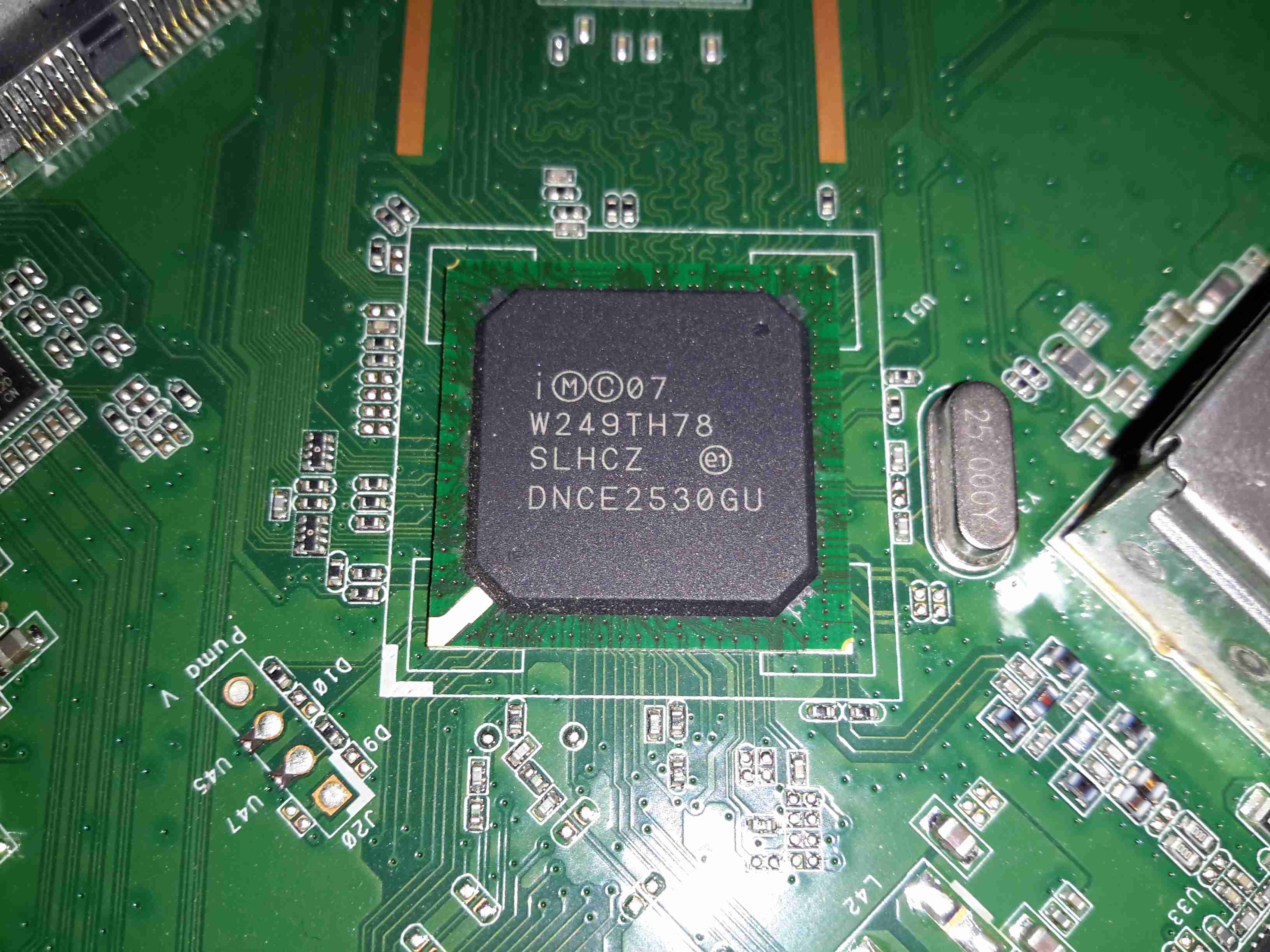
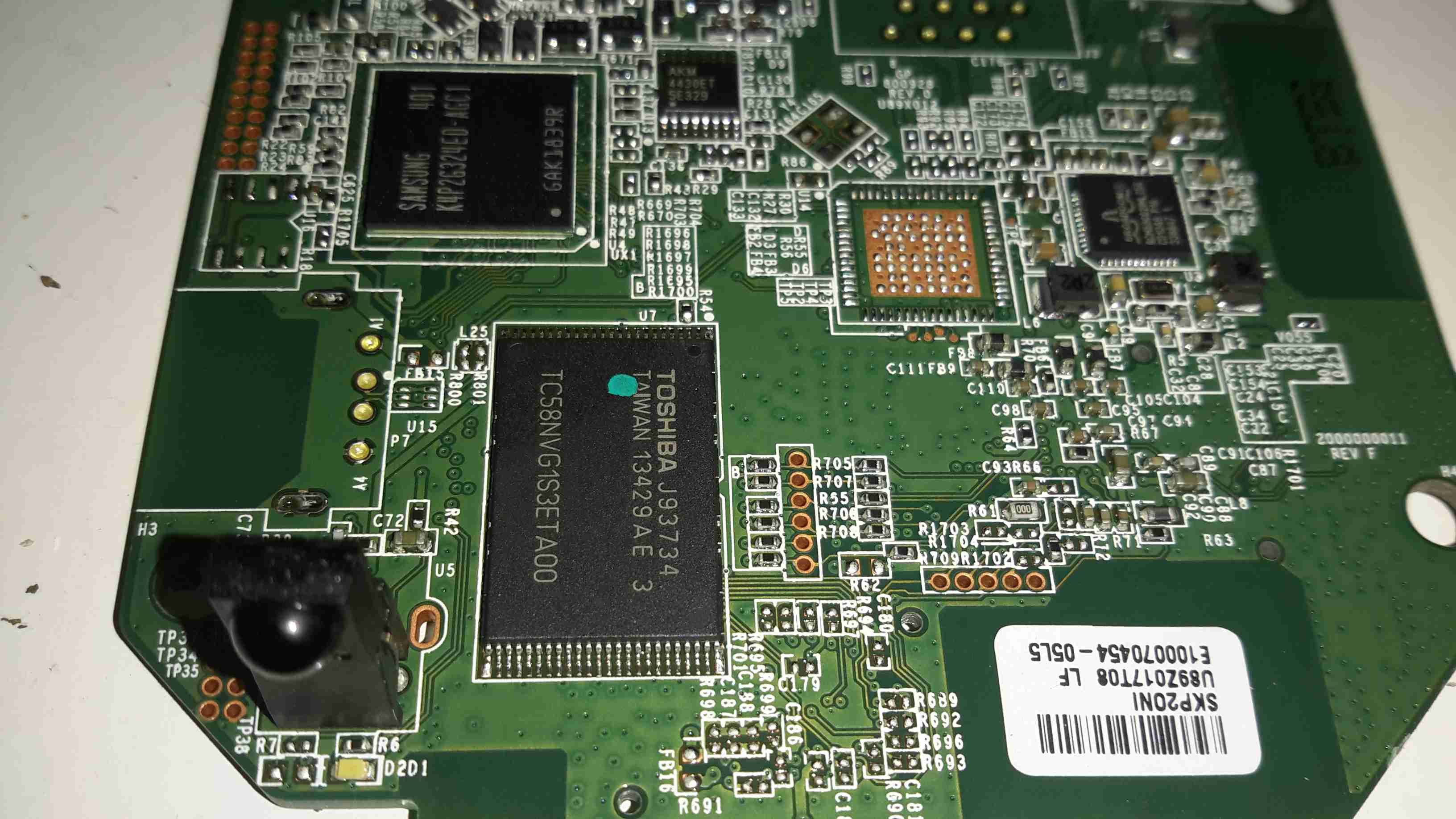
The cable modem side of things is taken care of by the Intel PUMA 5 DNCE2530GU SoC. This appears to communicate with the rest of the system via the Ethernet switch & PCI Express for the 5GHz radio.

Atheros WiFi SoC
Atheros WiFi SoC

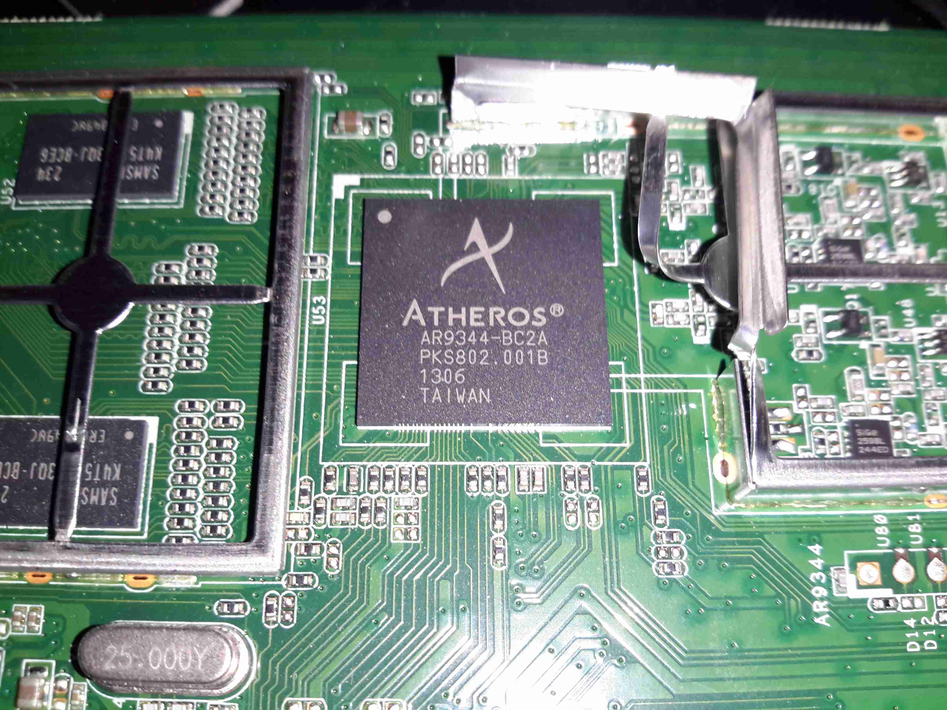
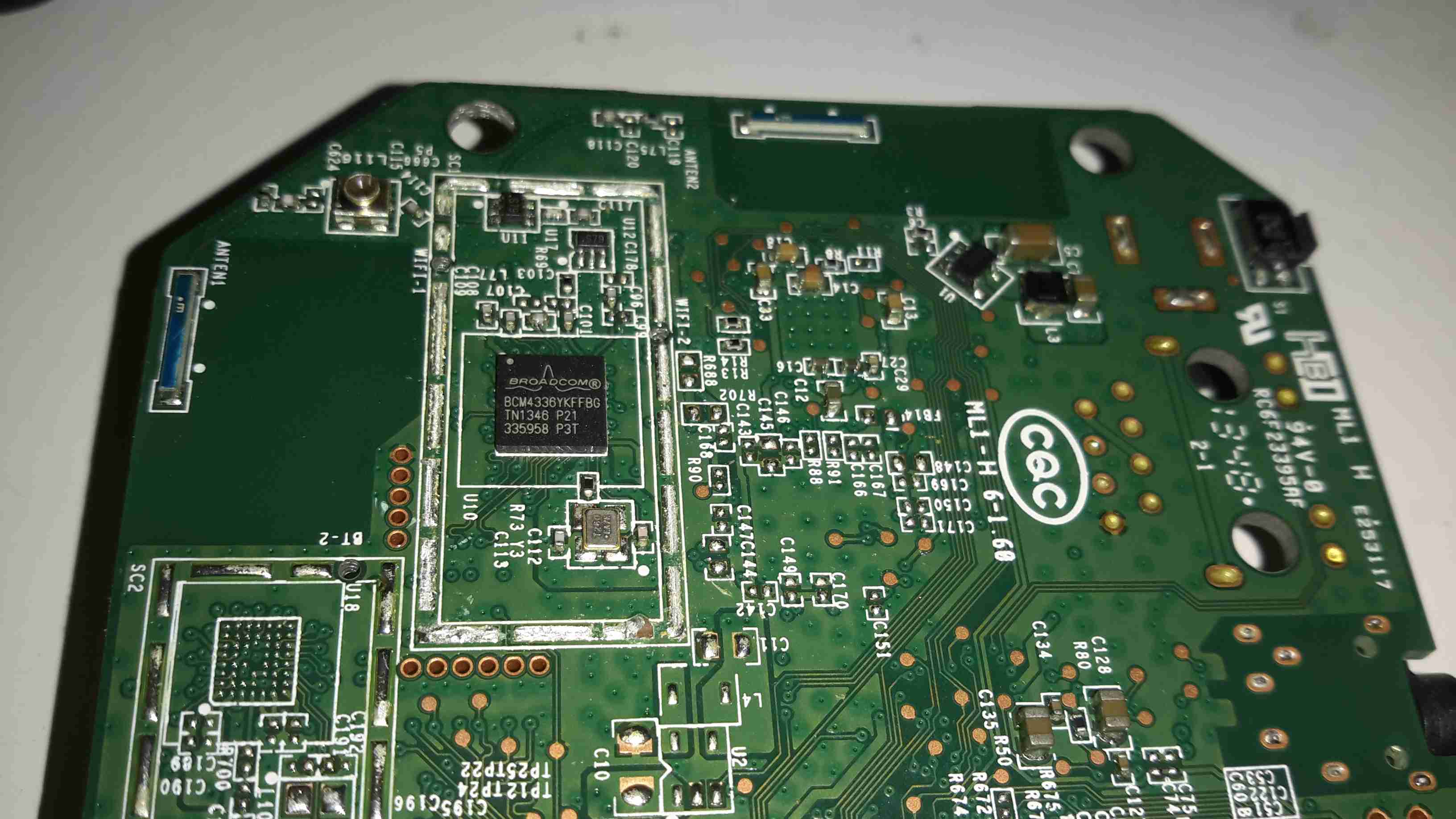
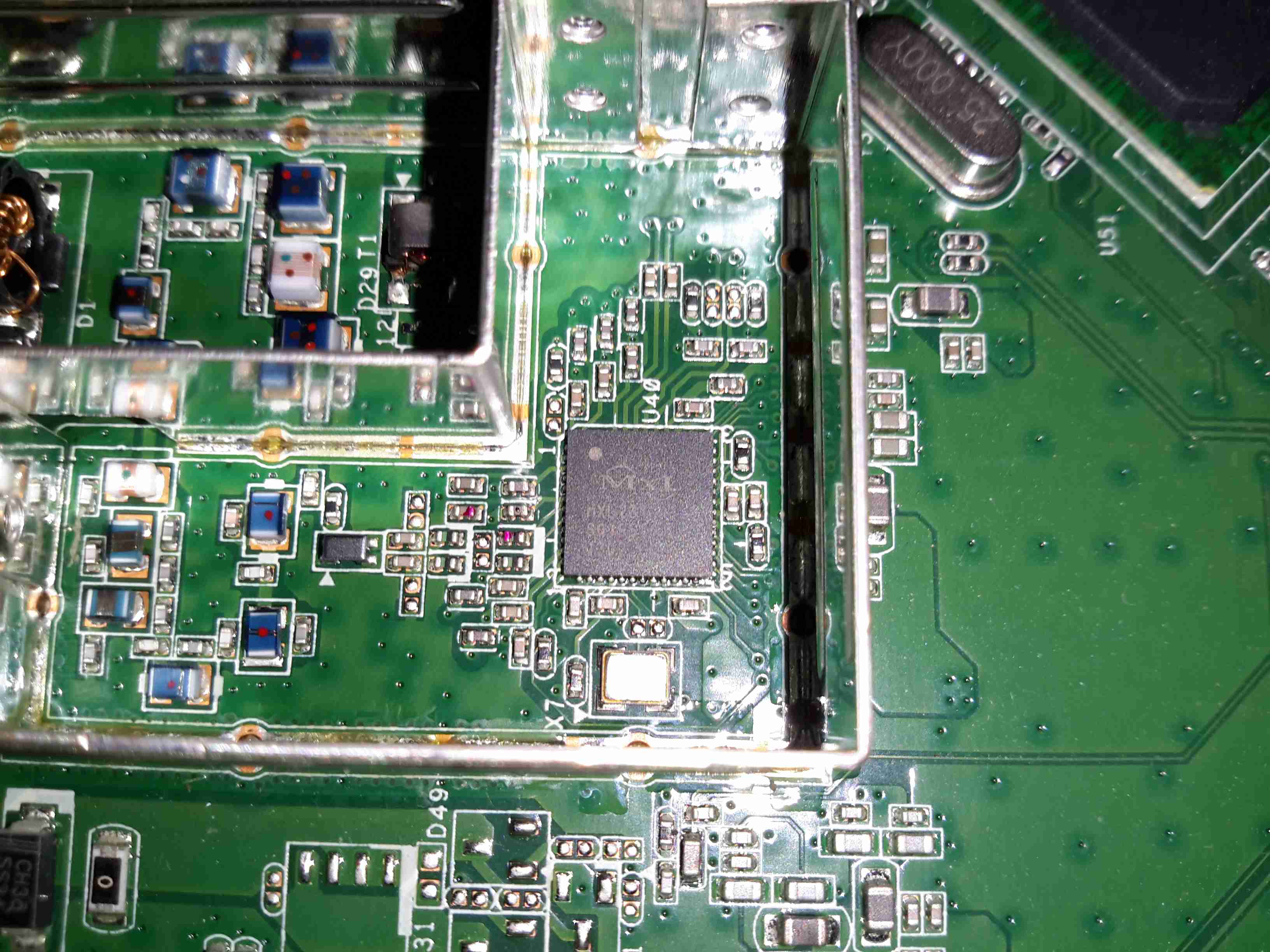
The 2.4GHz radio functionality is supplied by an Atheros AR9344 SoC, it’s RAM is to the left. This is probably handling all the router functions of this unit, but I can’t be certain.

Atheros LAN PHY
Atheros LAN PHY

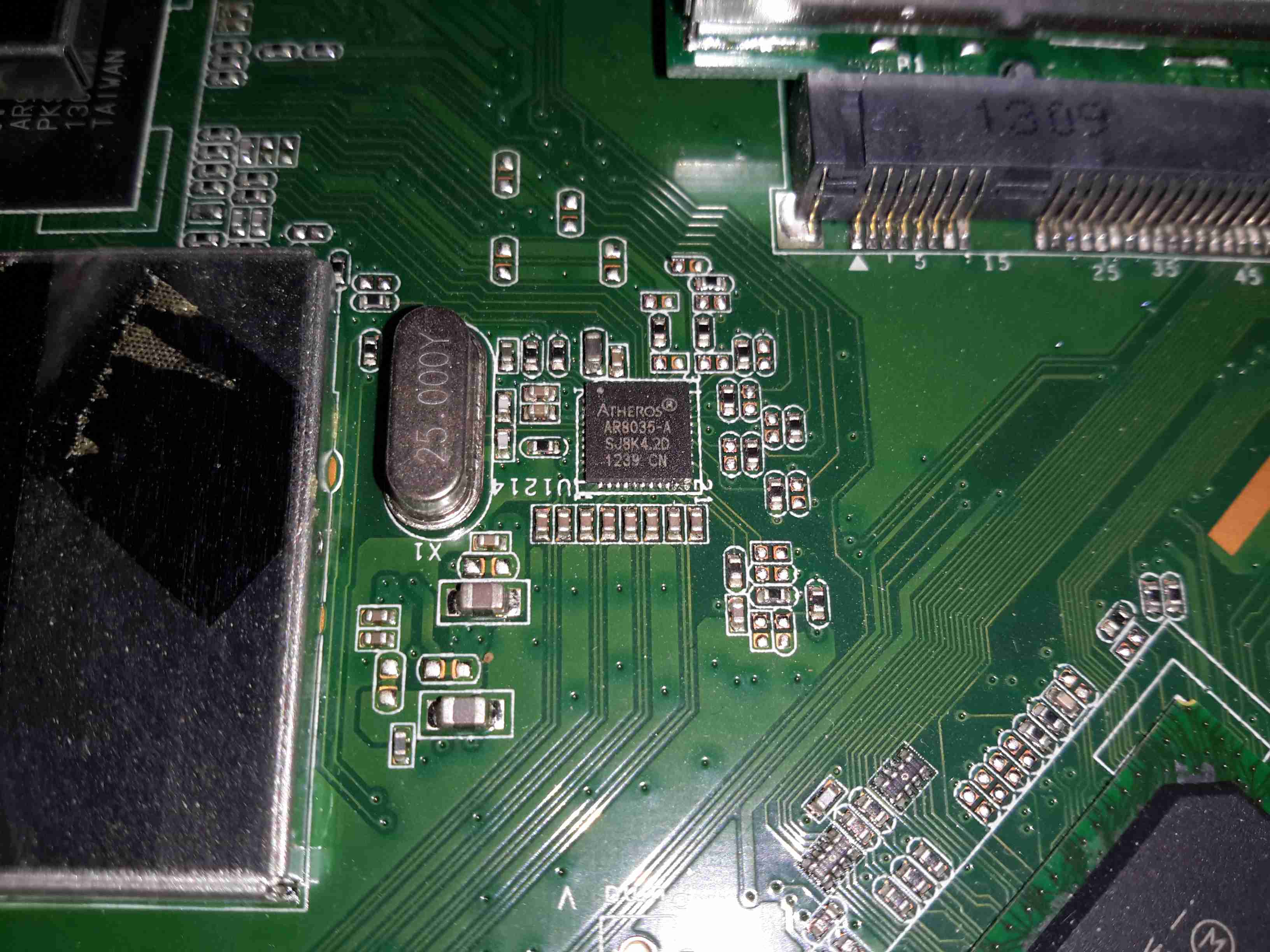
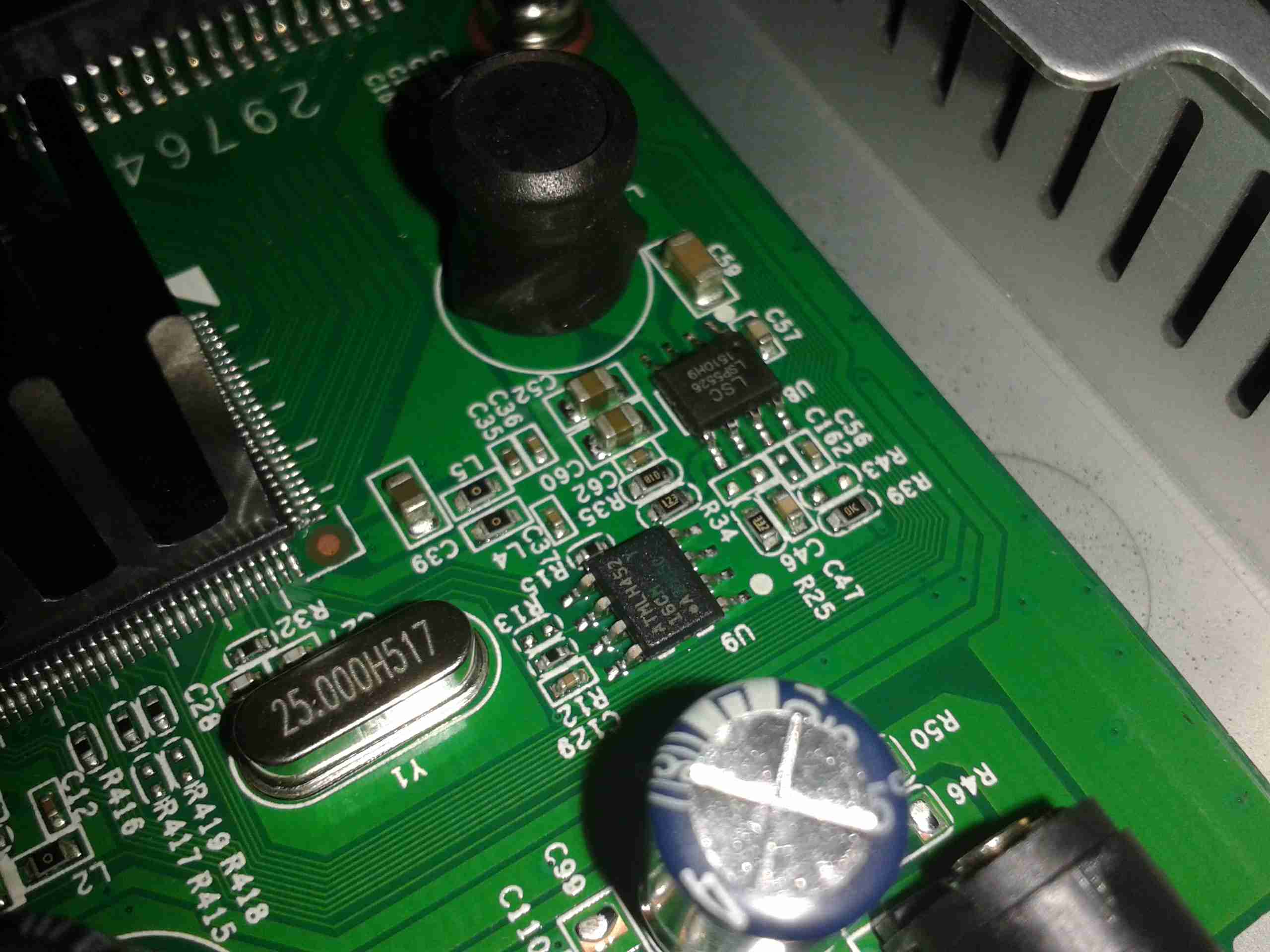
A separate Ethernet PHY is located between the SoC & the switch IC.


5GHz Radio Card
5GHz Radio Card

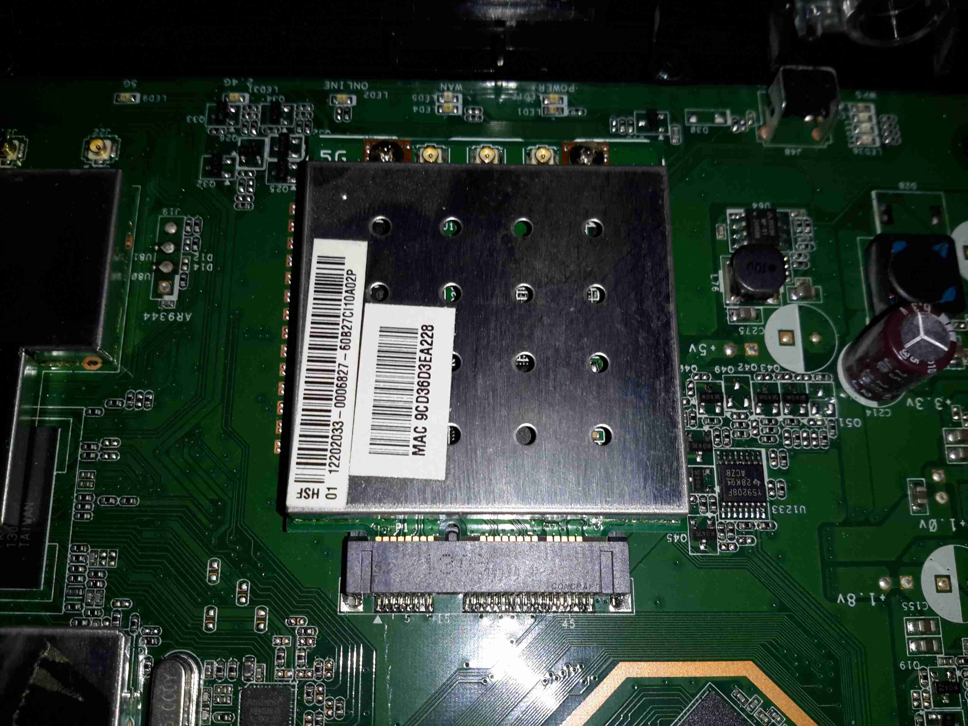
The 5GHz band is served by a totally separate radio module, in Mini PCIe format, although it’s a bit wider than standard. This module will probably be kept for reuse in another application.

Power Supplies
Power Supplies

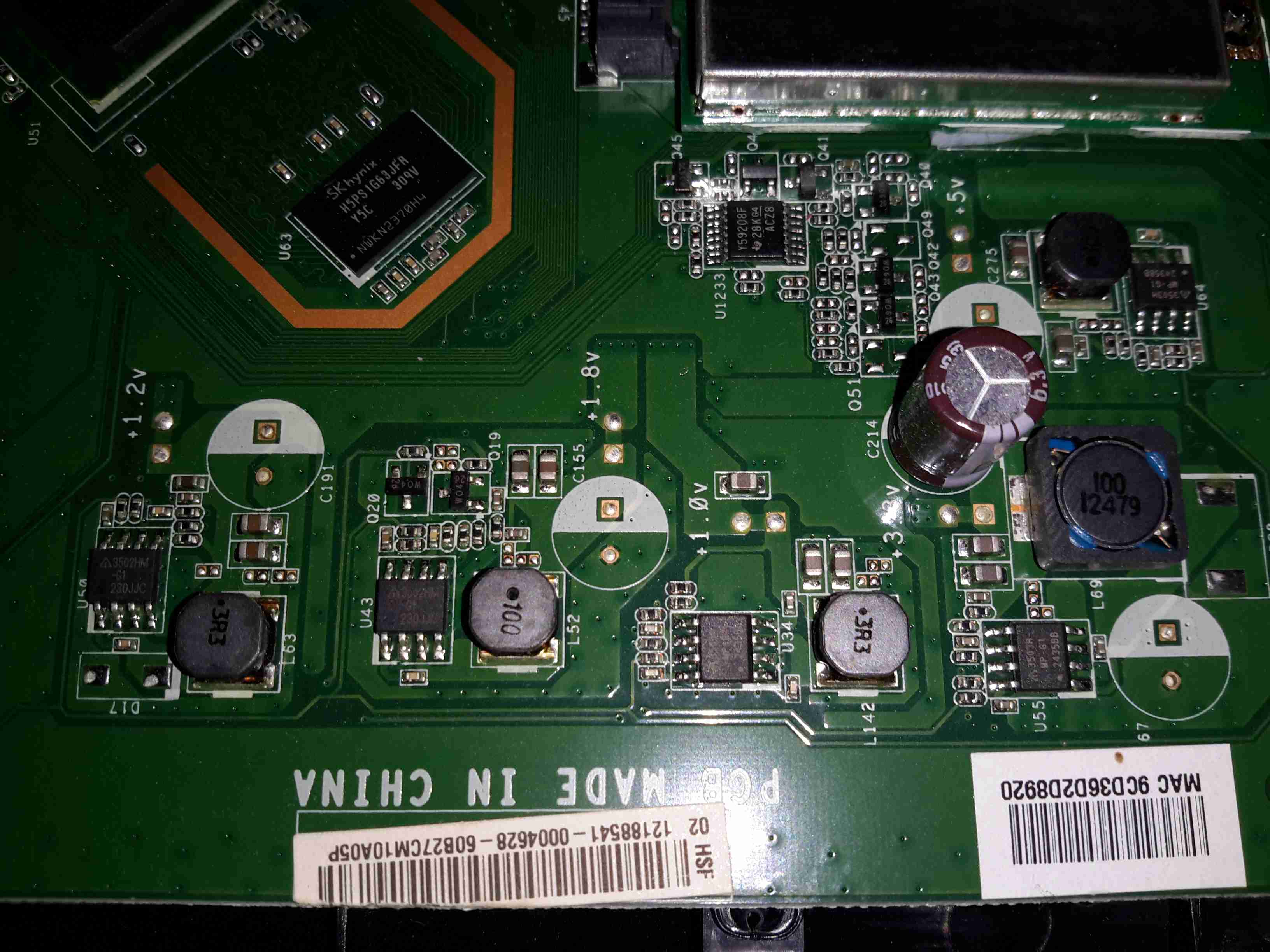
All down the edge of the board are the multiple DC-DC converters to generate the required voltage rails.

MaxLinear MXL261 Frontend

The DOCSIS frontend is handled by a MaxLinar MXL261 Tuner/Demodulator. More on this IC in my decapping post 🙂

The Unknown One
The Unknown One

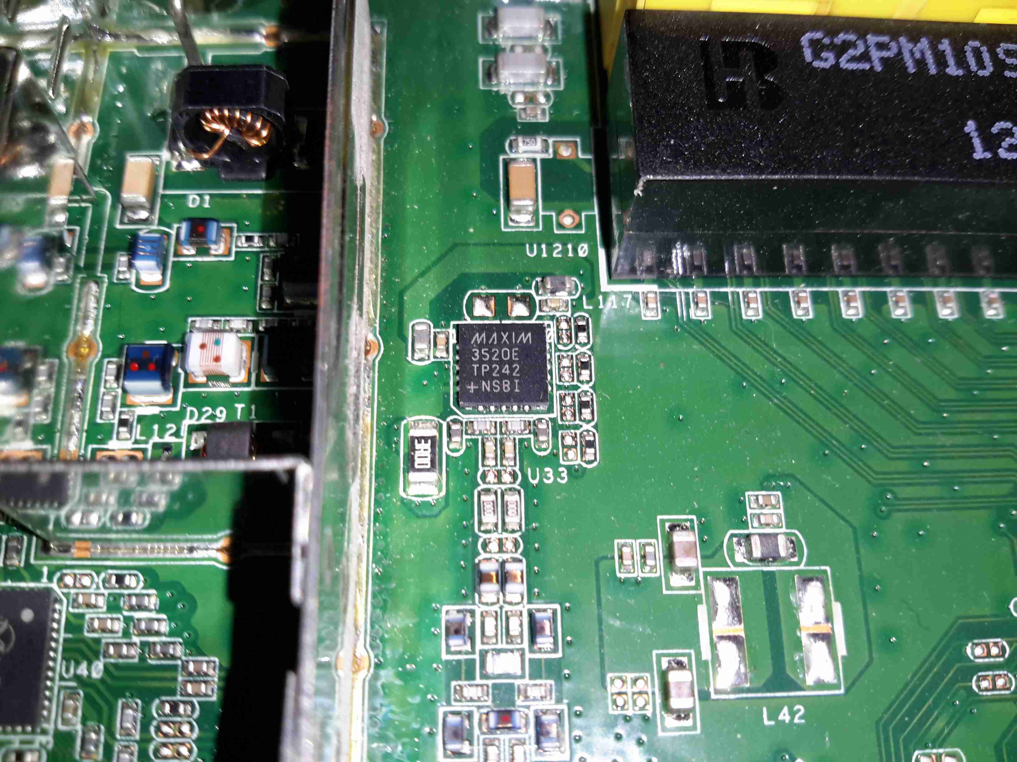
I’ve honestly no idea what on earth this Maxim component is doing. It’s clearly connected via an impedance matched pair, and that track above the IC looks like an antenna, but nothing I search for brings up a workable part number.

2.4GHz Frontend
2.4GHz Frontend

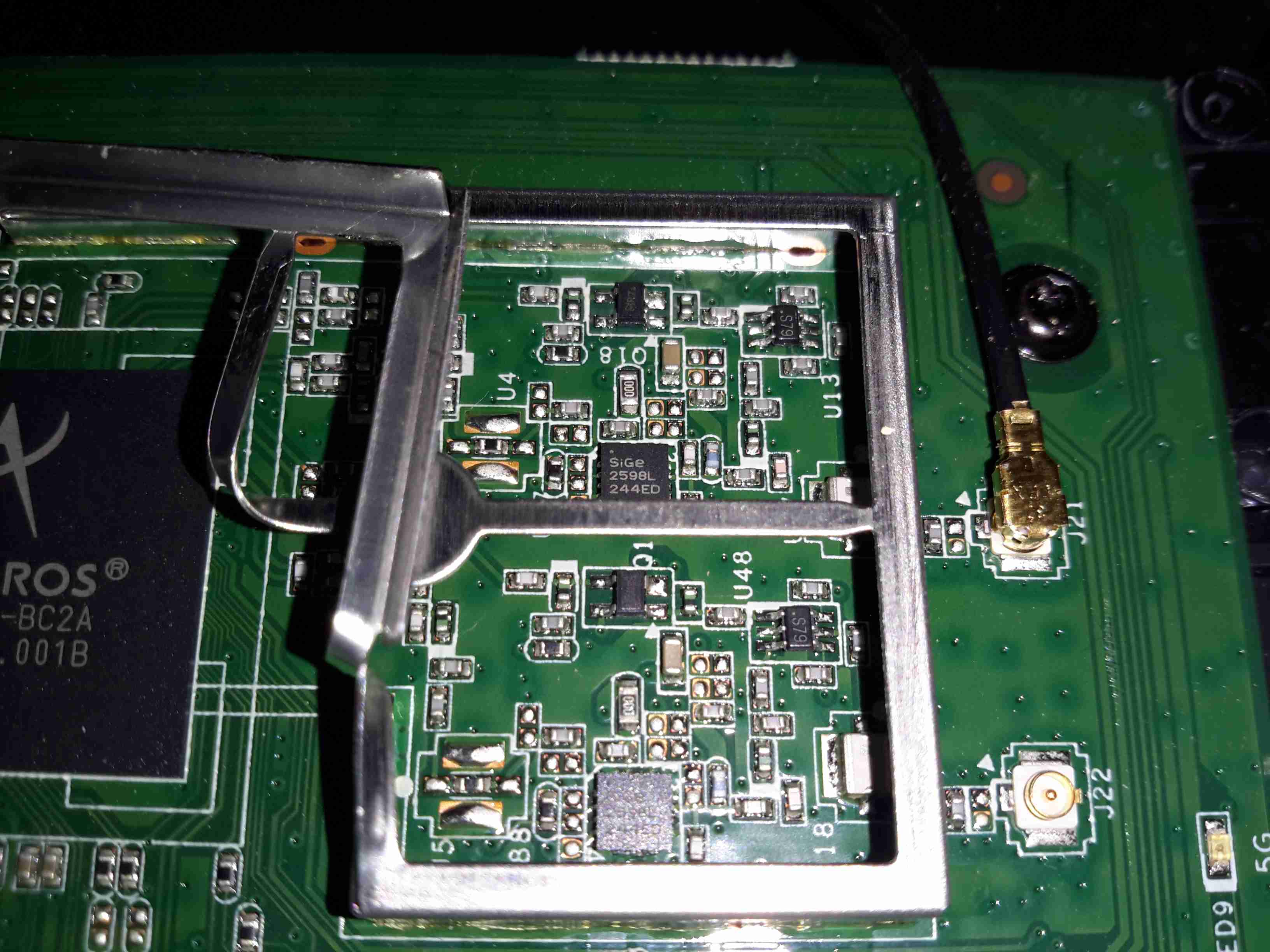
The RF switching & TX amplifiers are under a shield, these PA chips are SiGe parts.

Atheros 5GHz Radio
Atheros 5GHz Radio

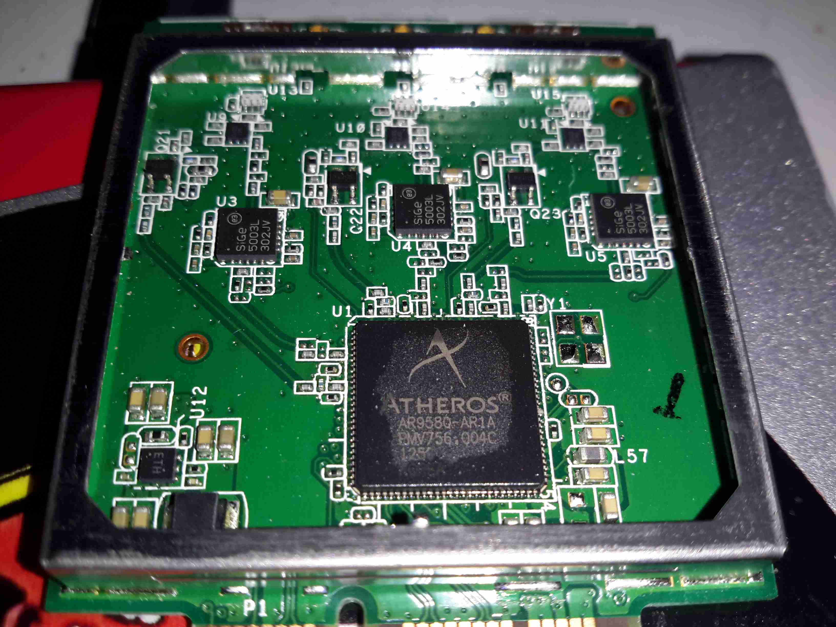
Pretty much the same for the 5GHz radio, but with 3 radio channels.

Posted on Leave a comment

AIX Gigabit Ethernet To USB Bridge

USB To Ethernet
USB To Ethernet

Here’s a chap eBay USB-To-Ethernet dongle I obtained for use with the Raspberry Pi Zero. This one is getting torn down permanently, as it’s rather unreliable. It seems to like having random fits where it’ll not enumerate on the USB bus. The silicon in the ICs will eventually make it here once I manage to get a new microscope 😉

Main Chipset
Main Chipset

This is quite a heavily packed PCB, with the main Asix AX88178 on the left. This IC contains all of the logic for implementing the Ethernet link over USB, except the PHY. It’s clock crystal is in the top left corner.

Reverse Side
Reverse Side

Not much on the reverse side, there’s a 3.3v linear regulator at top left, the SOIC is an Atmel AT93C66A 4KB EEPROM for configuration data.

Vitesse PHY
Vitesse PHY

The final IC in the chain is the Vitesse VSC8211 Gigabit PHY, with it’s clock crystal below. This interfaces the Ethernet MAC in the Asix IC to the magjack on the right.

Posted on 2 Comments

Roku LT Teardown


Roku LT
Roku LT

Here’s another retired piece of tech that we used to route media from the NAS to the main TV. It was retired since it’s inability to support XBMC/Kodi & having some crashing issues.

Main PCB
Main PCB

After attacking the case with the screwdriver (Torx in this case), the main board comes out. The CPU in this looks *very* familiar, being a PoP device. There are unpopulated places for an ethernet interface & USB port here.

Flash & CPU
Flash & CPU

After a little digging is turns out the CPU in this device is a BCM2835, with 256MB of RAM stacked on top. It’s a Raspberry Pi! Even the unpopulated part for Ethernet is the same SMSC LAN9512!
There’s 32MB of Flash for the software below the CPU.
On the far right of the board is a Broadcom BCM59002IML Mobile Power Management IC.

WiFi Chipset
WiFi Chipset

On the bottom of the PCB is the WiFi chipset, a Broadcom BCM4336, this most likely communicates with the CPU via SDIO. There’s also a section below for a Bluetooth chipset.


Posted on Leave a comment

Netgear GS308 Gigabit Switch

Here’s a new addition to the network, mainly to replace the ancient Cisco Catalyst 3500 XL 100MB switch I’ve been using for many years, until I can find a decently priced second hand commercial gigabit switch.

Operational
Operational

Here’s the switch with some network connections on test. So far it’s very stable & draws minimum power. I’ve not yet attempted to run my core links (NAS) through yet, as I’ve not yet seen a consumer grade switch that can stand up to constant full load without crashing.

Internals
Internals

Here’s the switch with it’s lid popped. The magnetics can be seen at the back, next to the RJ-45 ports, the large IC in the centre is the main switching IC, with a heatsink bonded to the top. Very minimal design, with only a couple of switching regulators for power supply & not much else.

Power & EEPROM
Power & EEPROM

Here’s a closeup of some of the support components. There’s a 25MHz crystal providing a clock signal for the switch IC, just to the right of that is an EEPROM. I imagine this is storing the switch configuration & MAC address. Further right is one of the switching DC-DC converter ICs for power.

As a quick test, here’s 500GB of data being shifted through the switch, at quite an impressive rate. I’m clearly maxing out the bandwidth of the link here. Soon I will upgrade to a 10G Ethernet link between the NAS & main PC to get some more performance.

Test
Test
Posted on 3 Comments

Evolis Dualys3 Card Printer Teardown

I recently dug out my other card printer to fit it with a 12v regulator, (it’s 24v at the moment), and figured I’d do a teardown post while I had the thing in bits.

This is a less industrial unit than my Zebra P330i, but unlike the Zebra, it has automatic duplexing, it doesn’t have Ethernet connectivity though.

Unlike domestic printers, which are built down to a price, these machines are very much built up to a spec, and feature some very high quality components.

Naked Printer
Naked Printer

Here’s the mechanism with the cowling removed. This is the main drive side of the printer, with the main drive stepper at left, ribbon take-up spool motor lower right, and the duplex module stepper motors at far right.

Main Motor Drive
Main Motor Drive

The main drive motor runs the various rollers in the card path through a pair of synchronous belts, shown here.

Main Stepper
Main Stepper

The stepper itself is a quality ball-bearing Sanyo Denki bipolar motor.

Main Stepper Driver
Main Stepper Driver

Electrical drive is provided to the stepper with a L6258EX DMOS universal motor driver. This chip can also drive DC motors as well as steppers.

Ribbon Supply Spool
Ribbon Supply Spool

Here is the encoder geared onto the ribbon supply spool. This is used to monitor the speed the ribbon is moving relative to the card.

Printer Top
Printer Top

Here’s a top view through the printer, the blue roller on the left cleans the card as it’s pulled from the feeder, the gold coloured spool to it’s right is the ribbon supply reel. The cooling fan on the right serves to stop the print head overheating during heavy use.

Spool Take Up Motor
Spool Take Up Motor

The spool take-up reel is powered by another very high quality motor, a Buhler DC gearmotor. These printers are very heavily over engineered!
This motor drives the spool through an O-Ring belt, before the gear above. This allows the drive to slip in the event the ribbon jams, preventing it from breaking.

Duplex Unit Stepper Drivers

The pair of steppers that operate the duplexing unit are driven by a separate board, with a pair of L6219DS bipolar stepper driver ICs. There are also a couple of opto-sensors on this board for the output hopper.


Main Control PCB
Main Control PCB

All the mechanisms of the printer are controlled from this main PCB, which handles all logic & power supply functions. Sections on the board are unpopulated, these would be for the Ethernet interface, smart card programming & magstripe programming.

Main CPU
Main CPU

The brains of the operation is this ColdFire MCF5208CVM166 32-bit microprocessor. It features 16KB of RAM, 8KB of cache, DMA controller, 3 UARTs, SPI, 10/100M Ethernet and low power management. This is a fairly powerful processor, running at 166MHz.
It’s paired with an external 128Mbit SDRAM from Samsung, and a Spansion 8Mbit boot sector flash, for firmware storage.

USB Interface & Power Input

Here the USB interface IC is located. It’s a USBN9604 from Texas Instruments, this interfaces with the main CPU via serial.

Posted on Leave a comment

PCMCIA Ethernet Card

Front
Front

An old Xircom Ethernet card for a laptop. This uses the old 50 pin PCMCIA interface.

Rear
Rear

Rear of the card with the MAC address & card spec details.

PCB
PCB

PCB removed from the outer shield. Xircom ethernet chipset centre. Special socket on the right fits a RJ-45 adaptor lead.