Posted on 10 Comments

Sony PS3 APS-231 Power Supply Voltage Mod

PSU Ratings
PSU Ratings
PSU Ratings

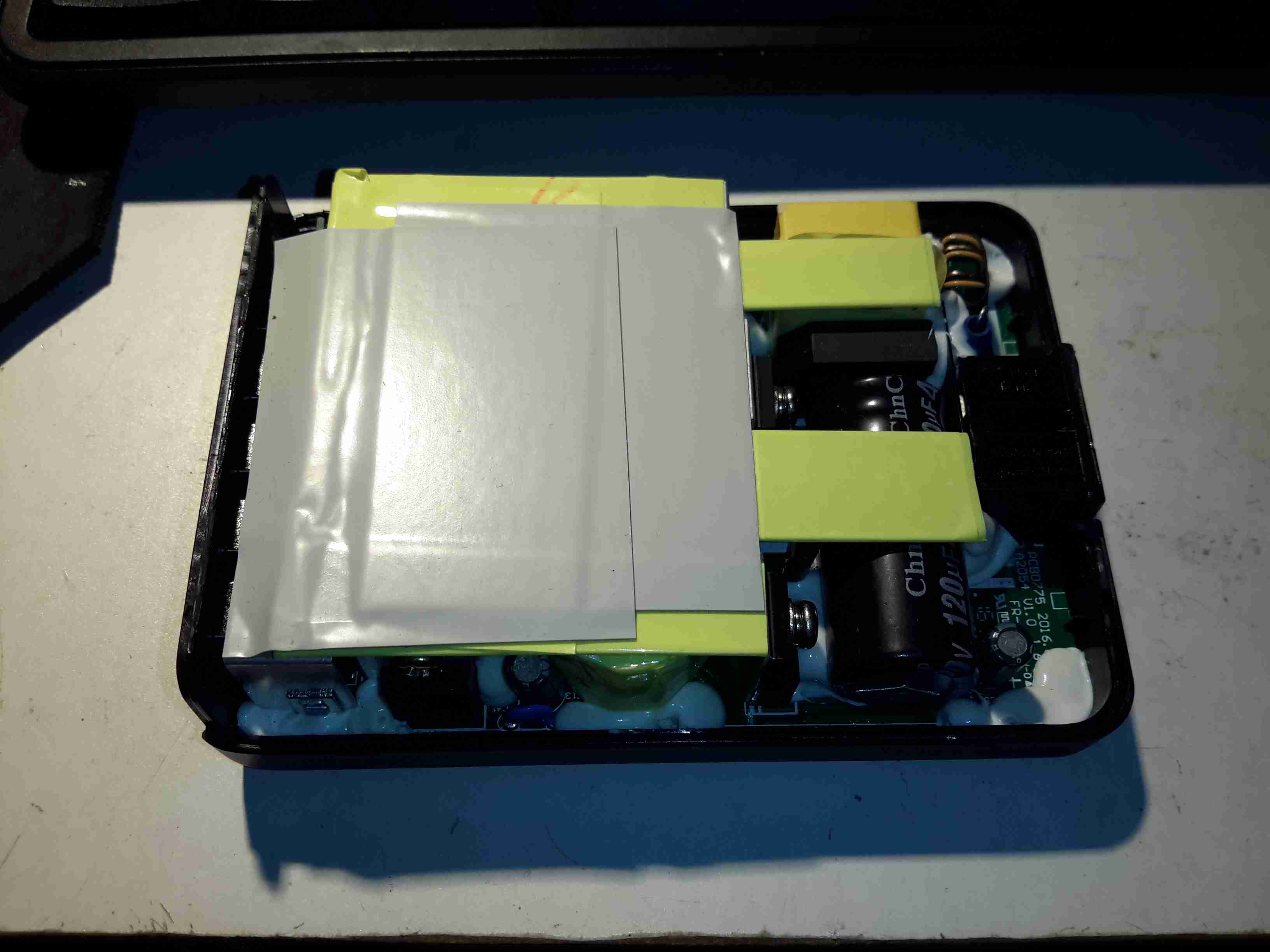
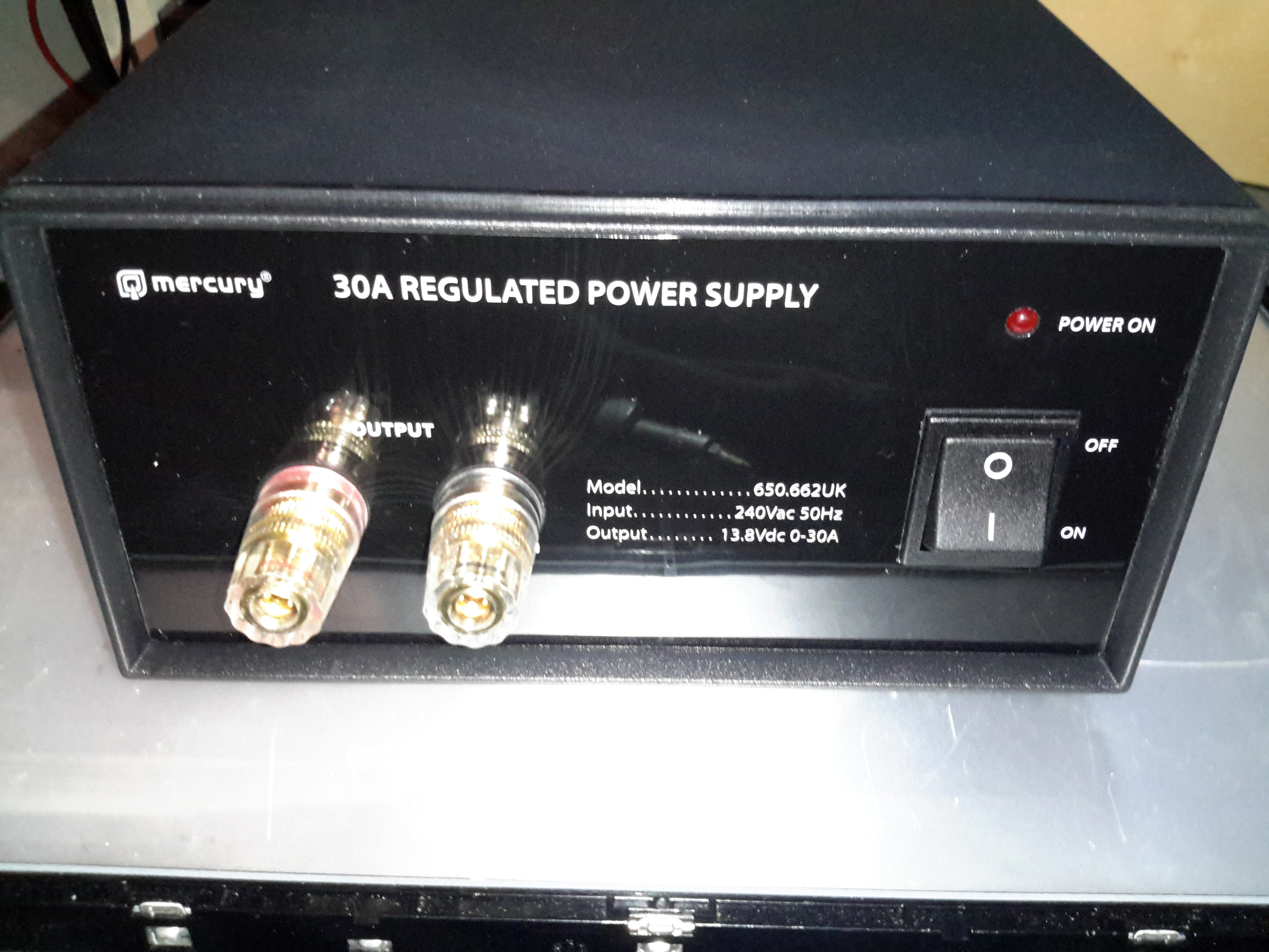
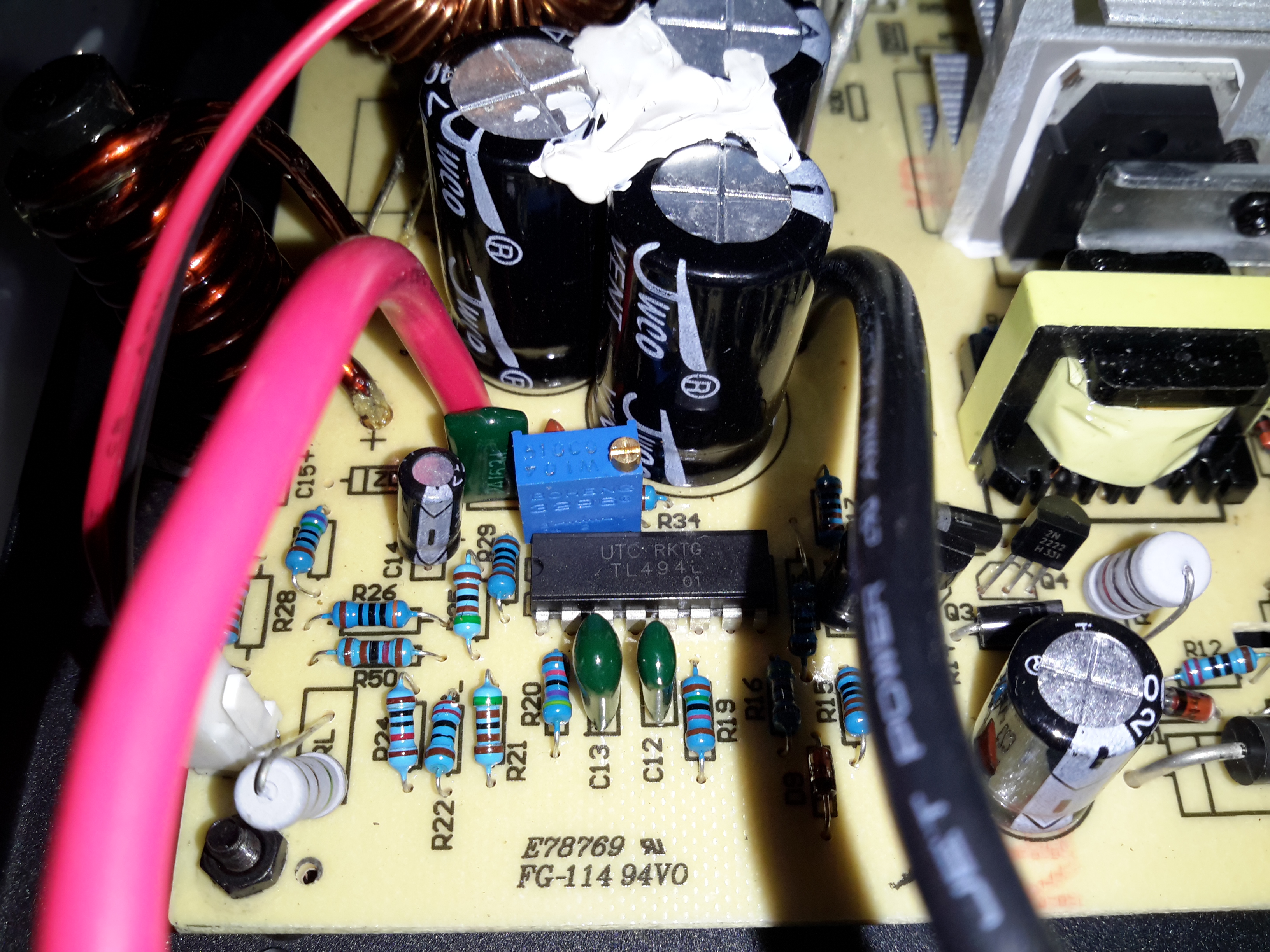
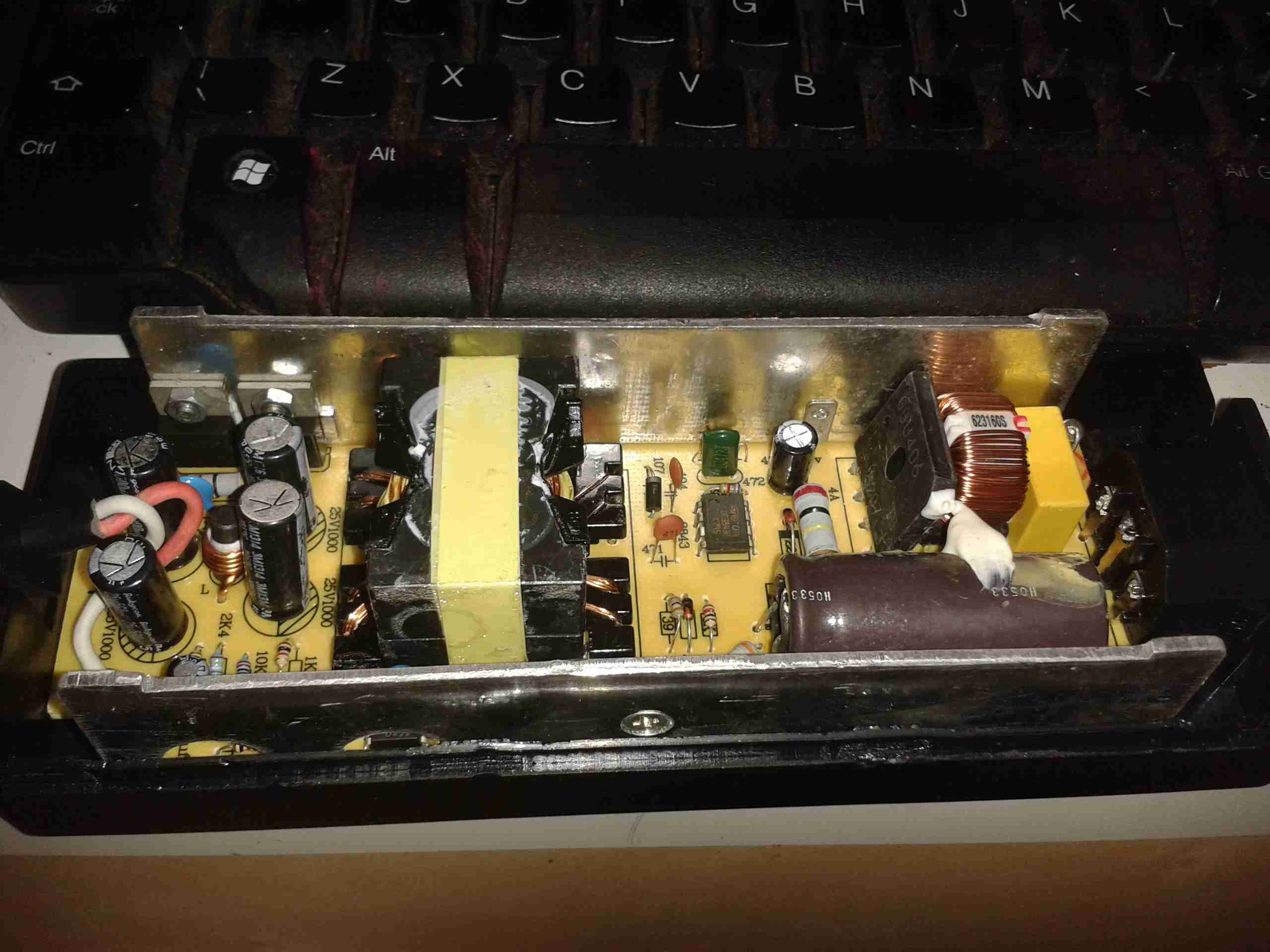
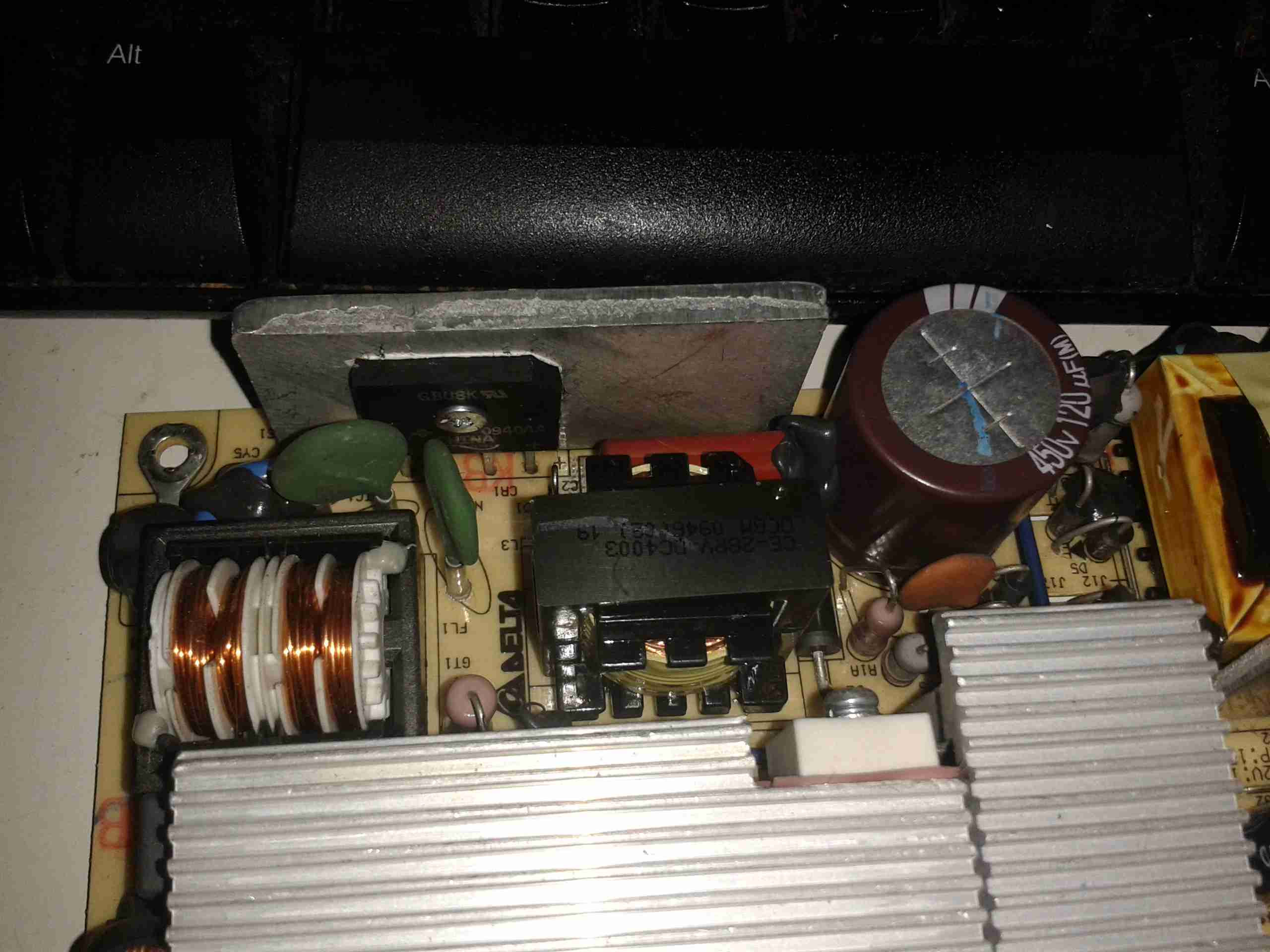
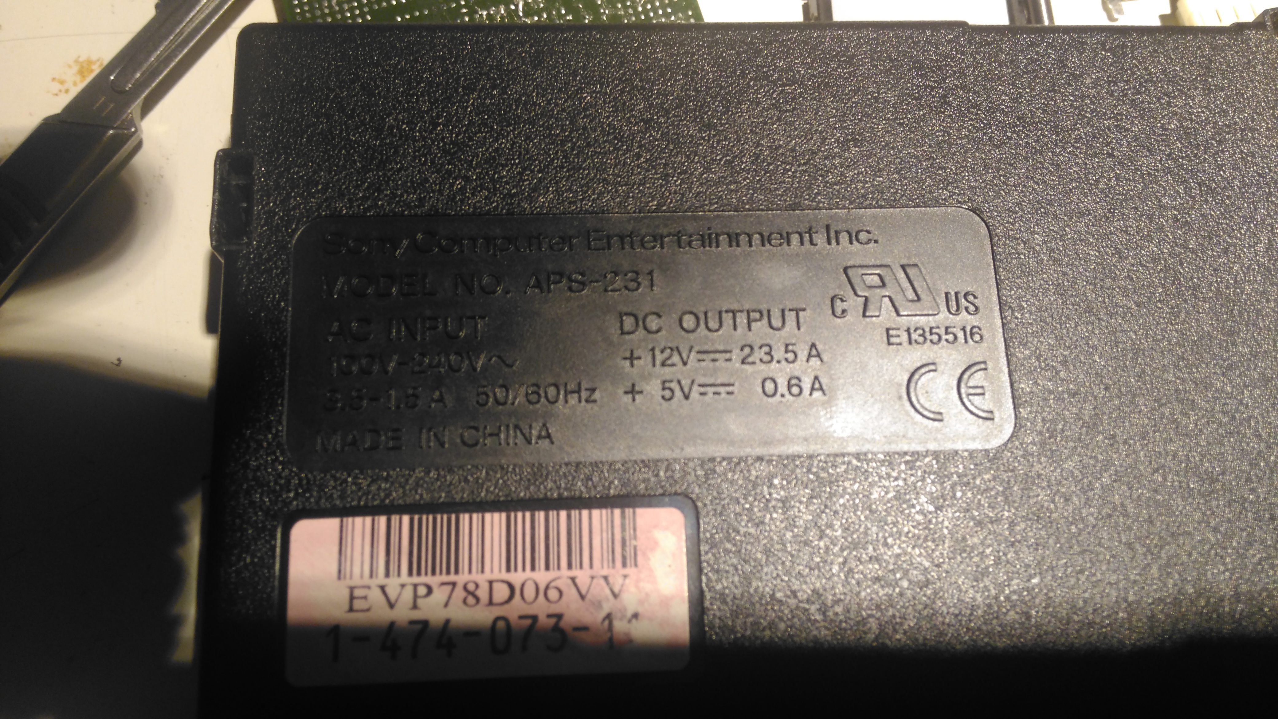
I was recently given a Sony PS3 with a dead disc drive, and since I’m not a console gamer I figured I’d see if there were any handy parts inside. Turns out these units contain a rather nice SMPS, the Sony APS-231 with a high power 12v rail, rated at 23.5A. A bit of searching around discovered a thread on the BadCaps Forums about voltage modding these supplies for a 13.8v output, suitable for my Ham radio gear.
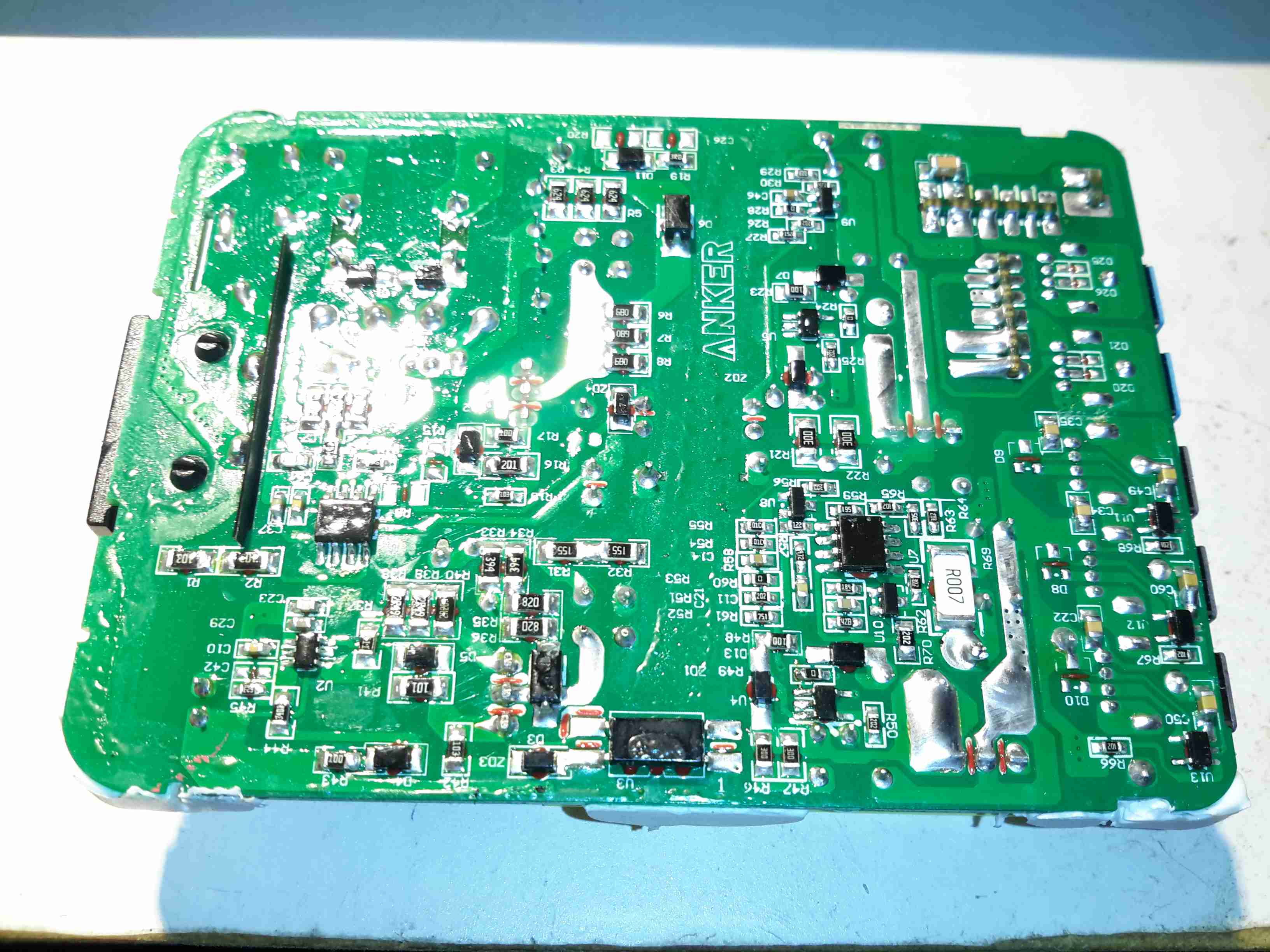
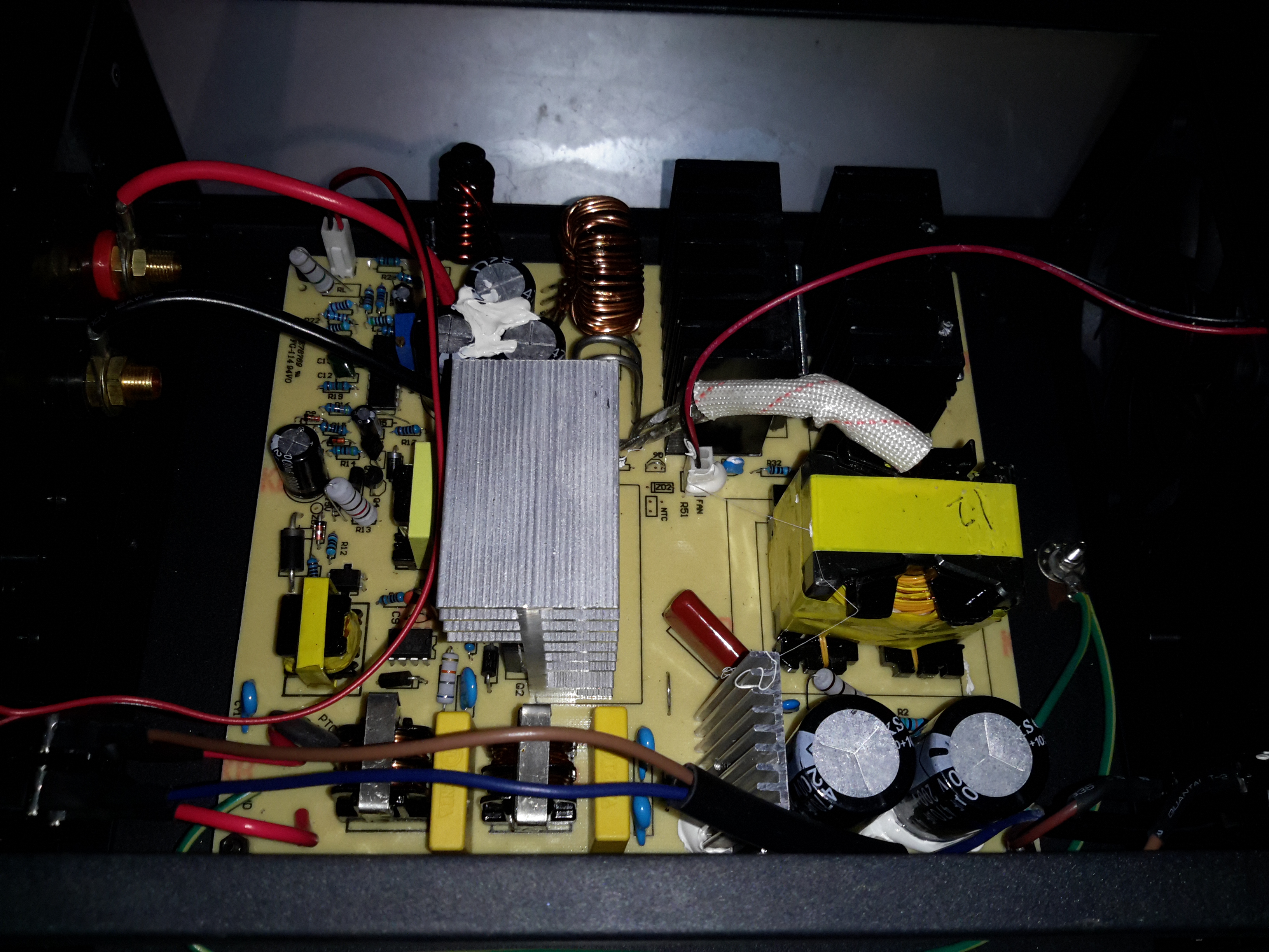
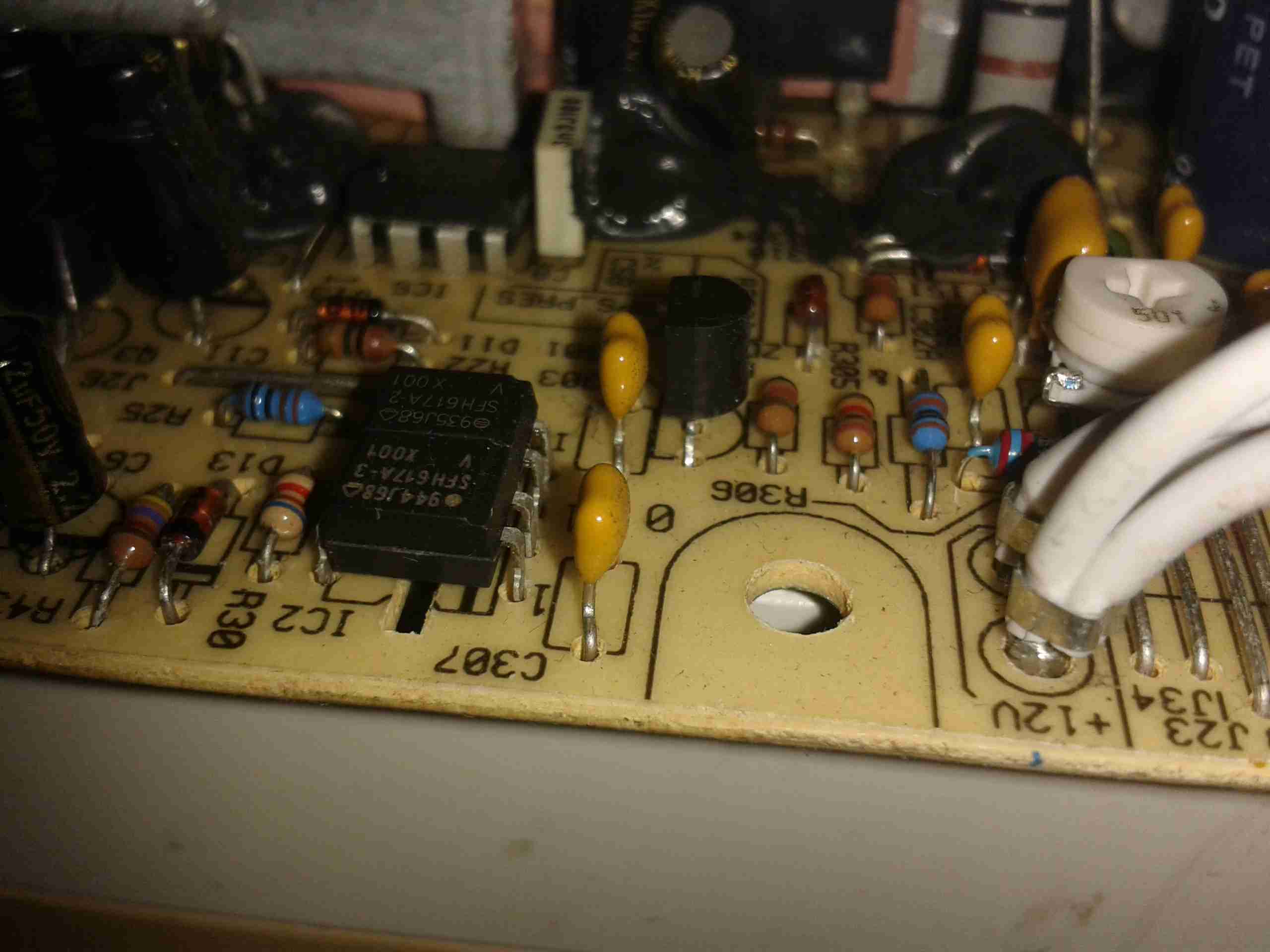
These supplies are controlled by a Sony CXA8038A, for which there is very little information. Active PFC is included, along with synchronous rectification which increases the efficiency of the supply, and in turn, reduces the waste heat output from the rectifiers.

Regulation Section
Regulation Section

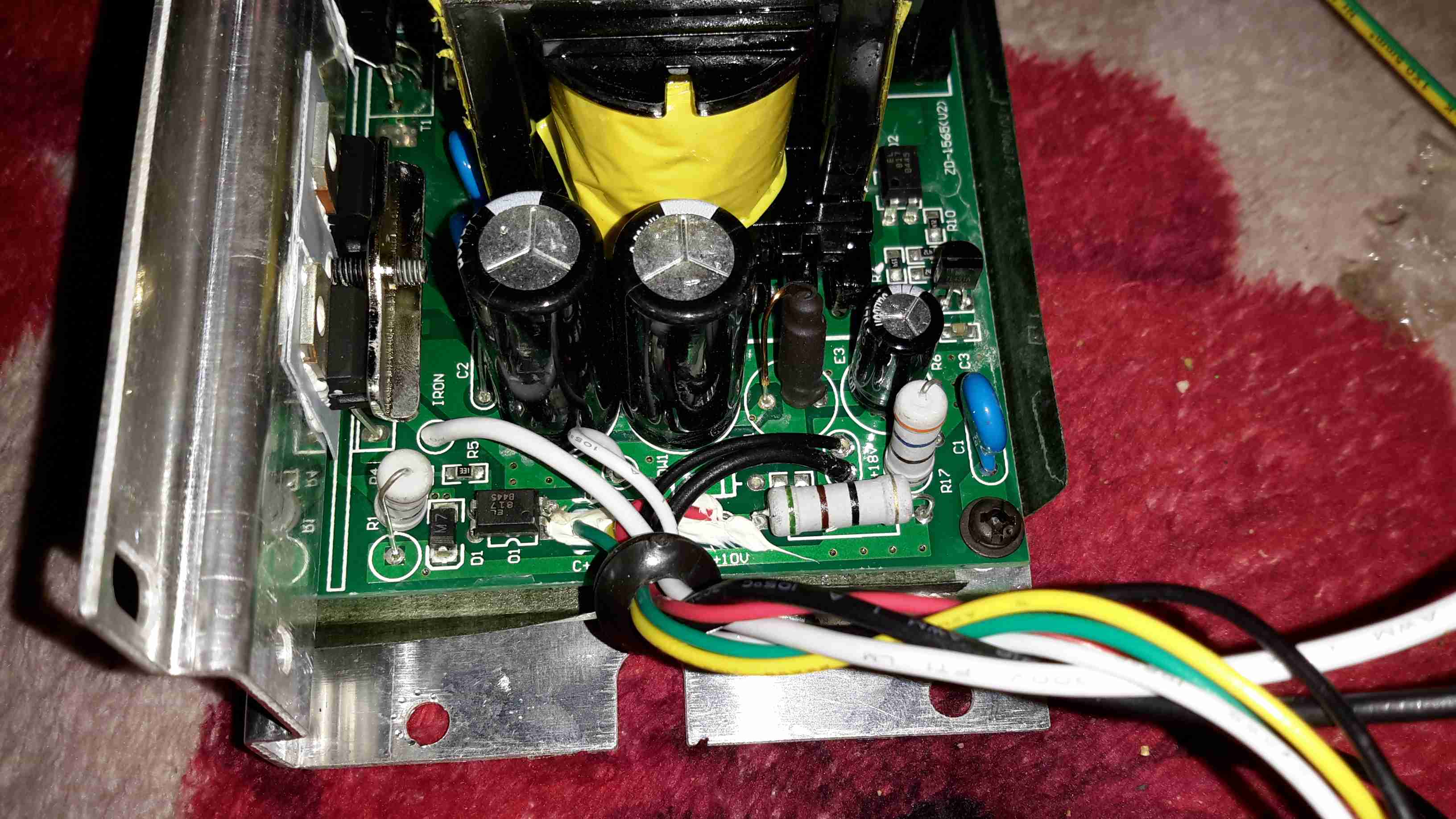
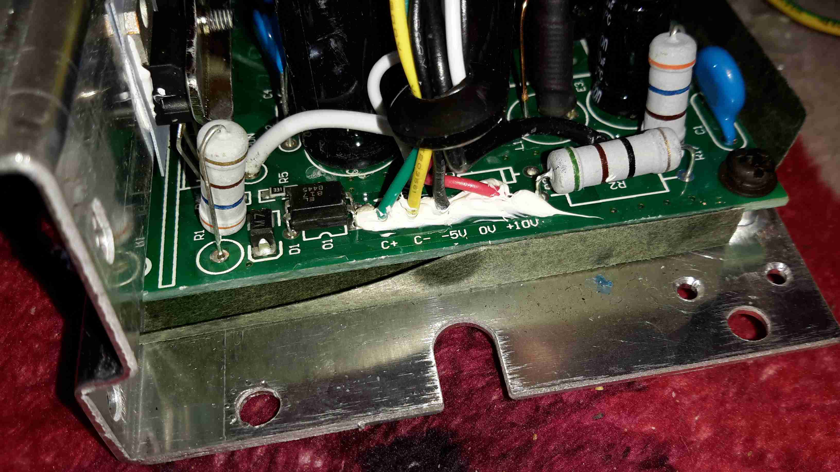
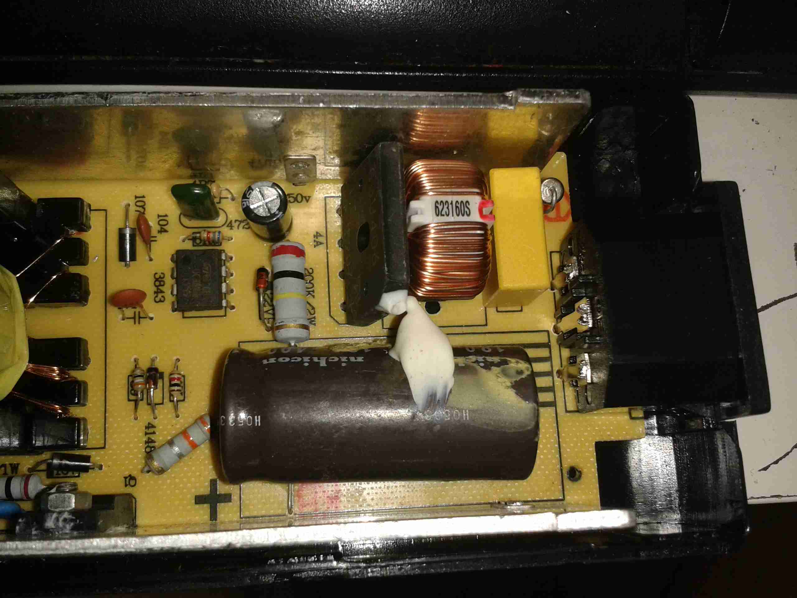
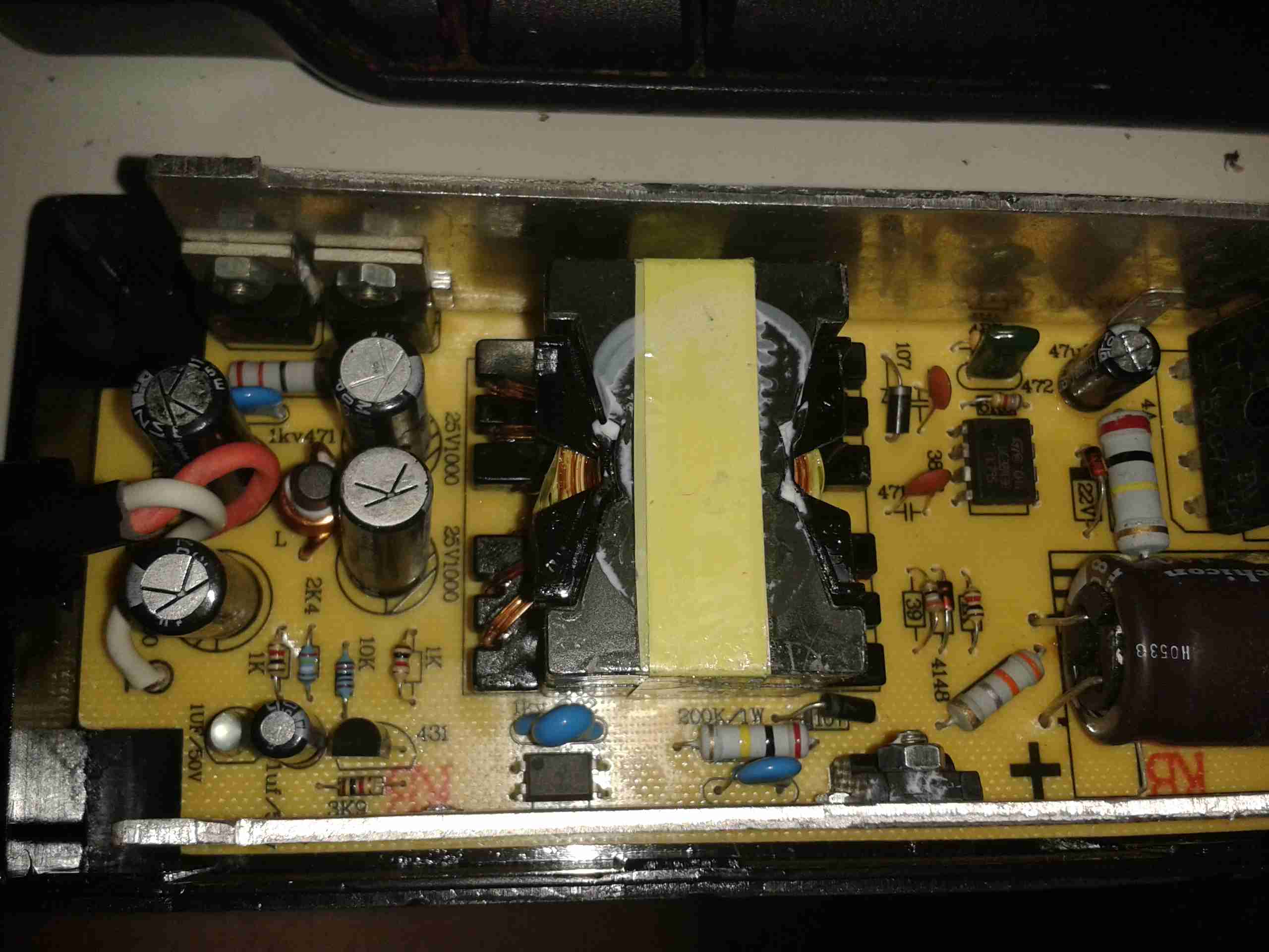
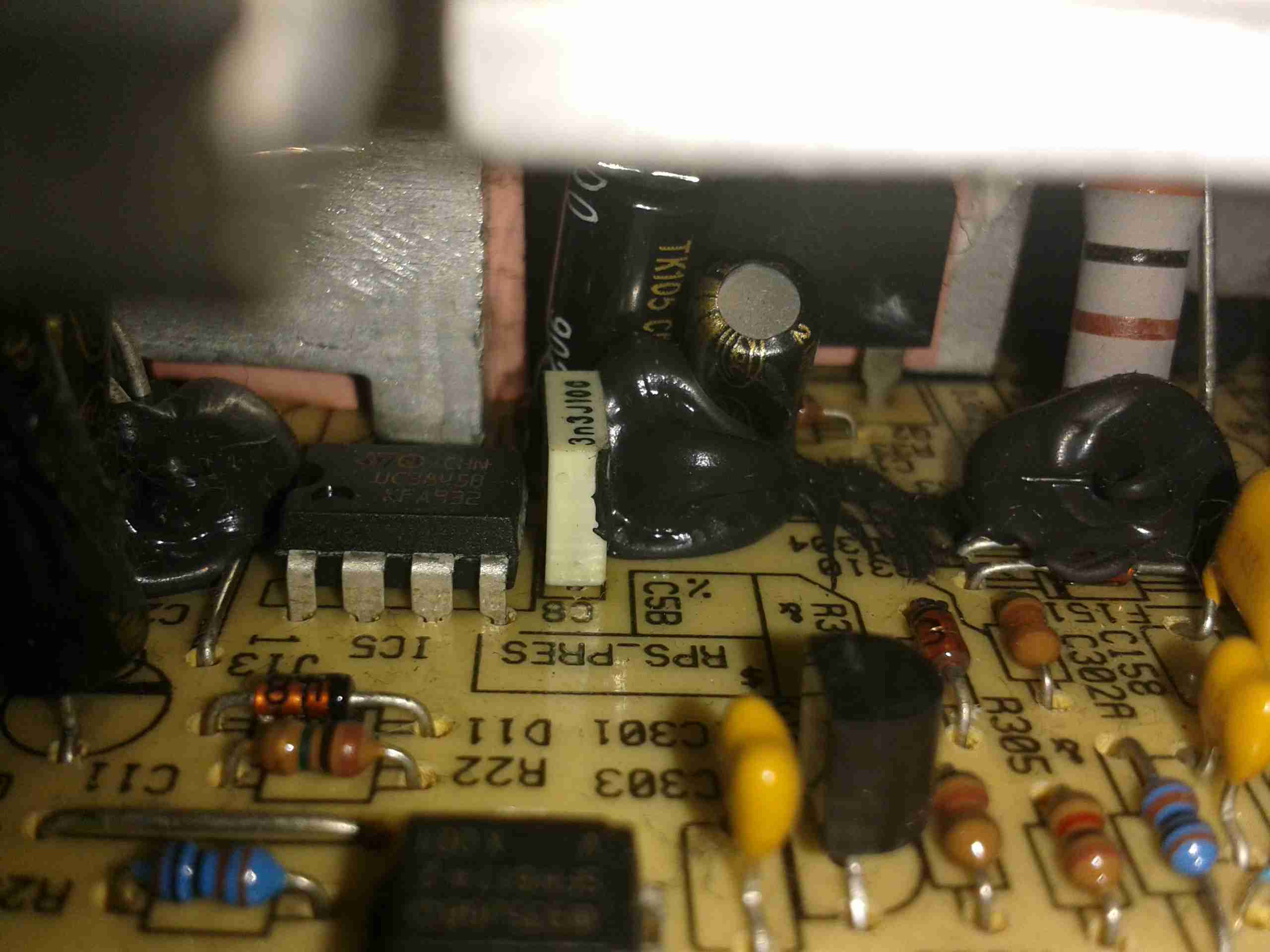
Like many of the SMPS units I’ve seen, the output voltage is controlled by referencing it to an adjustable shunt reference, and adjusting the set point of this reference will in turn adjust the output voltage of the supply, this is done in circuit by a single resistor.

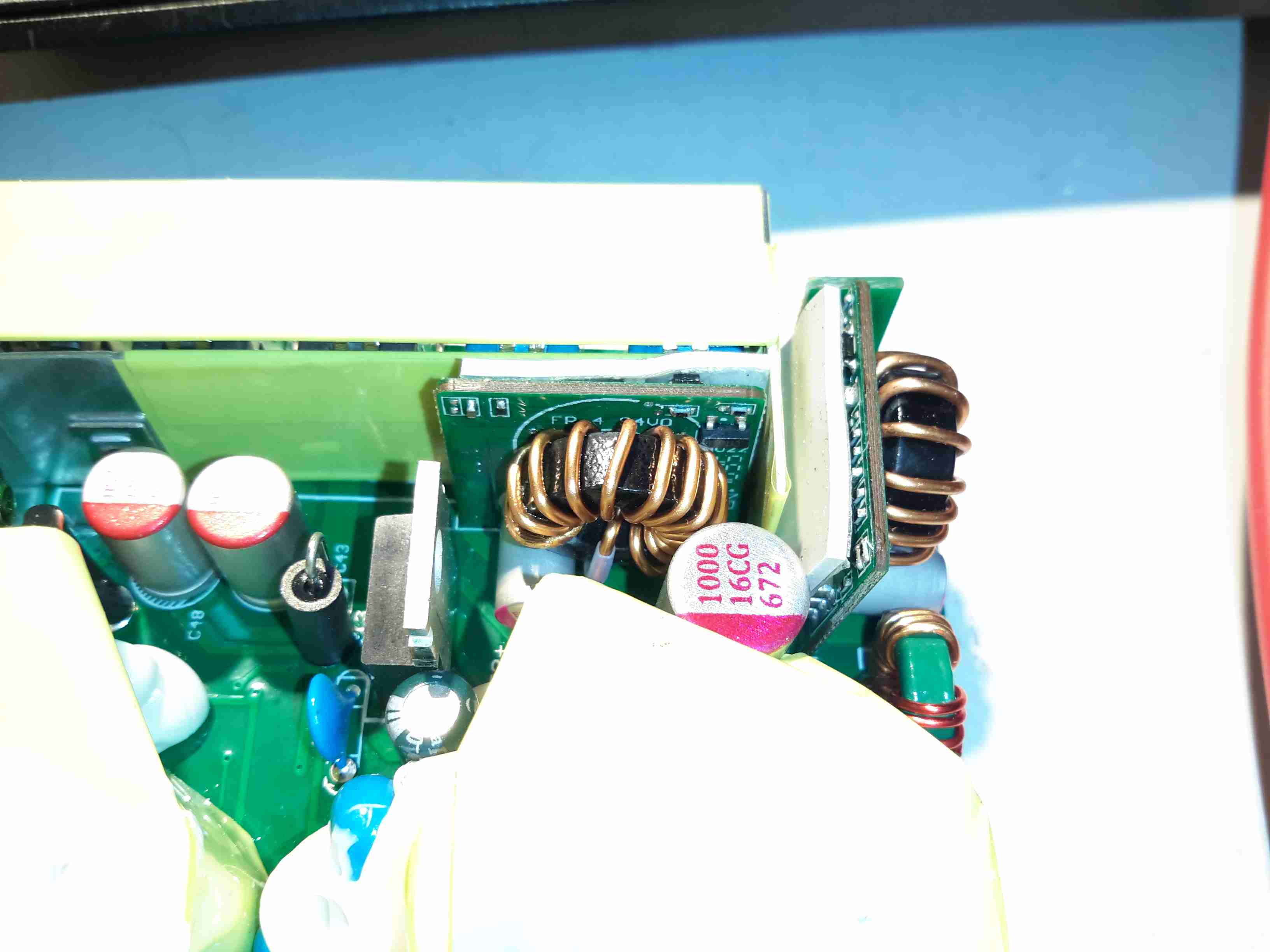
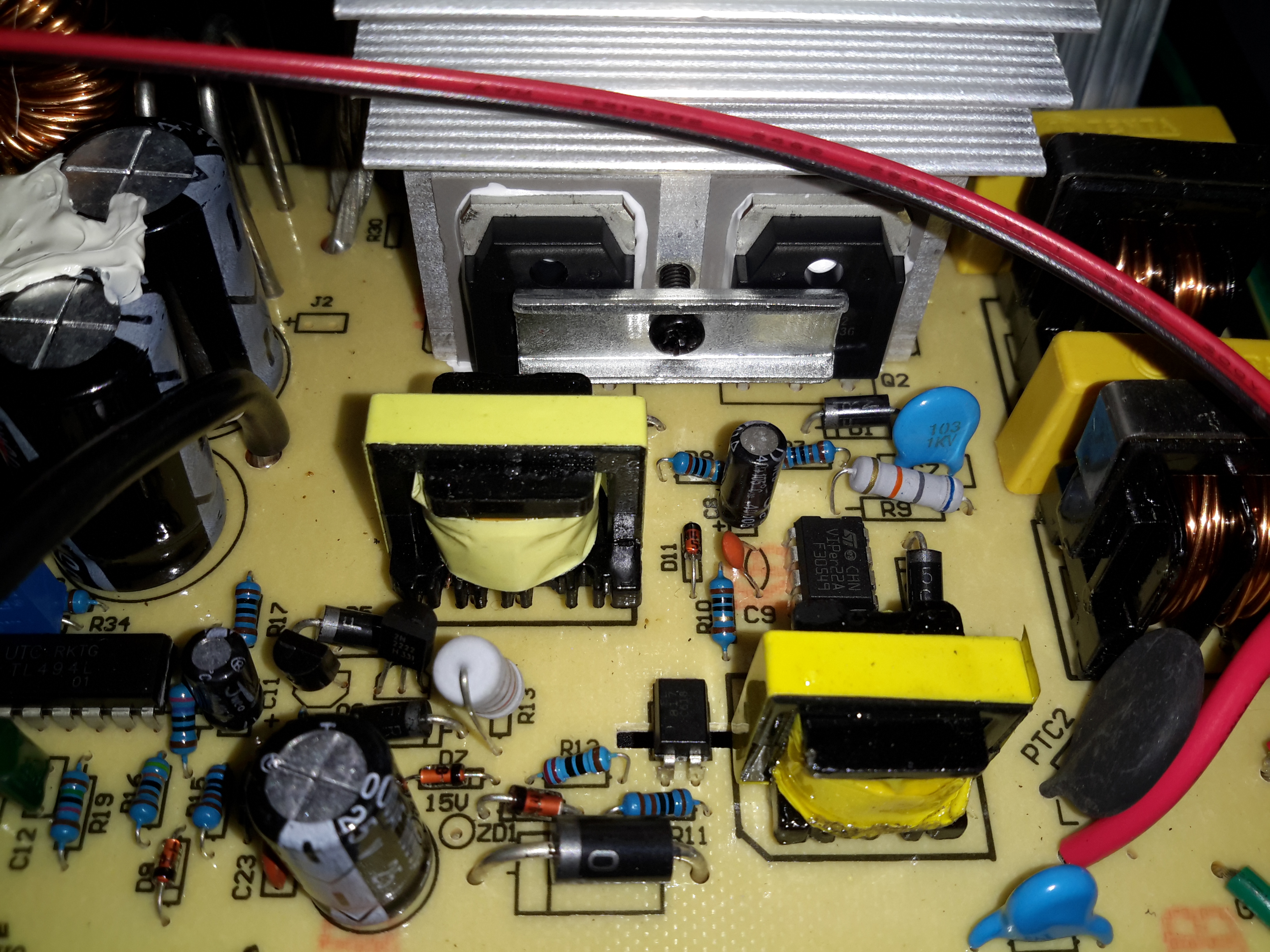
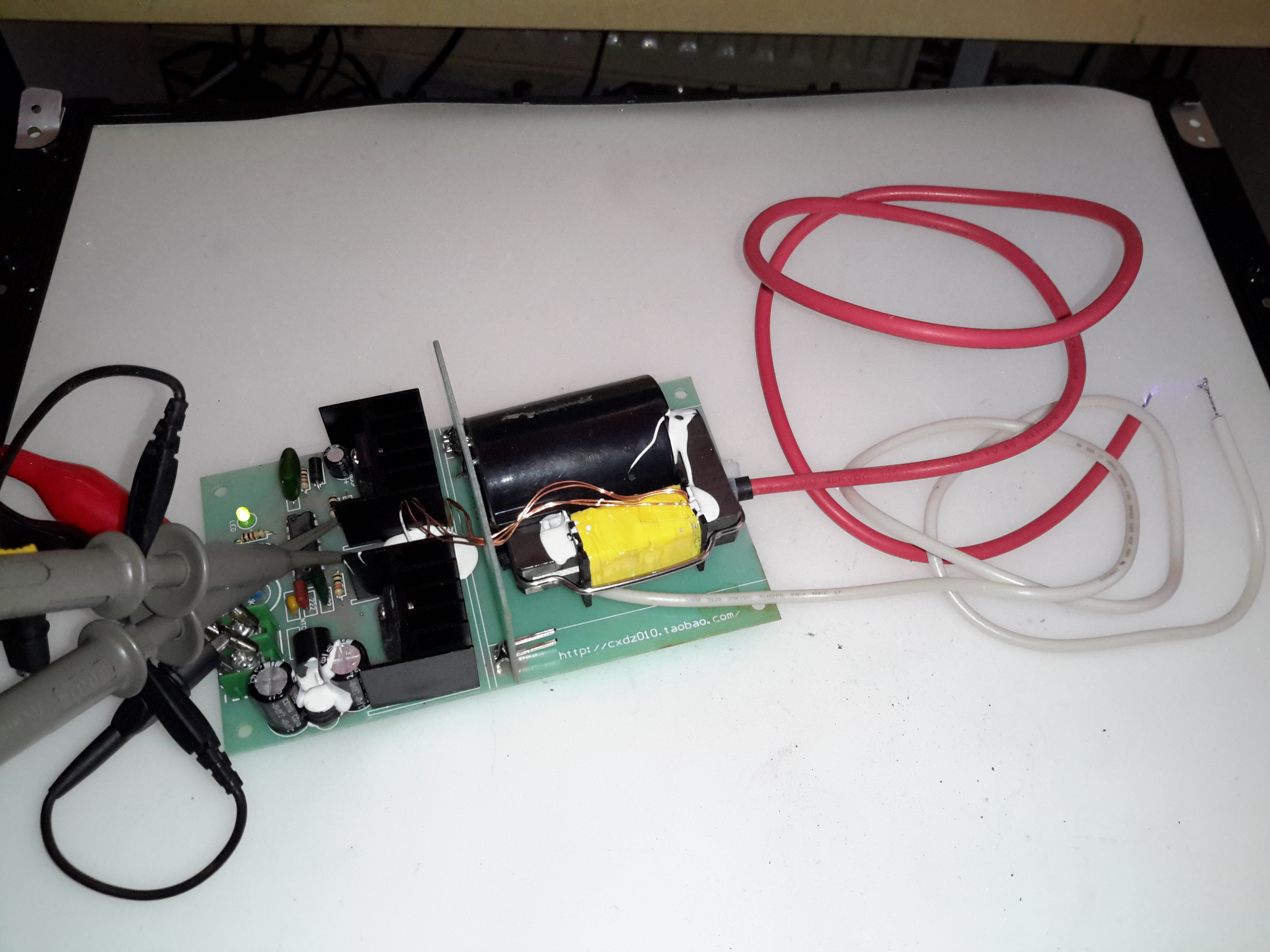
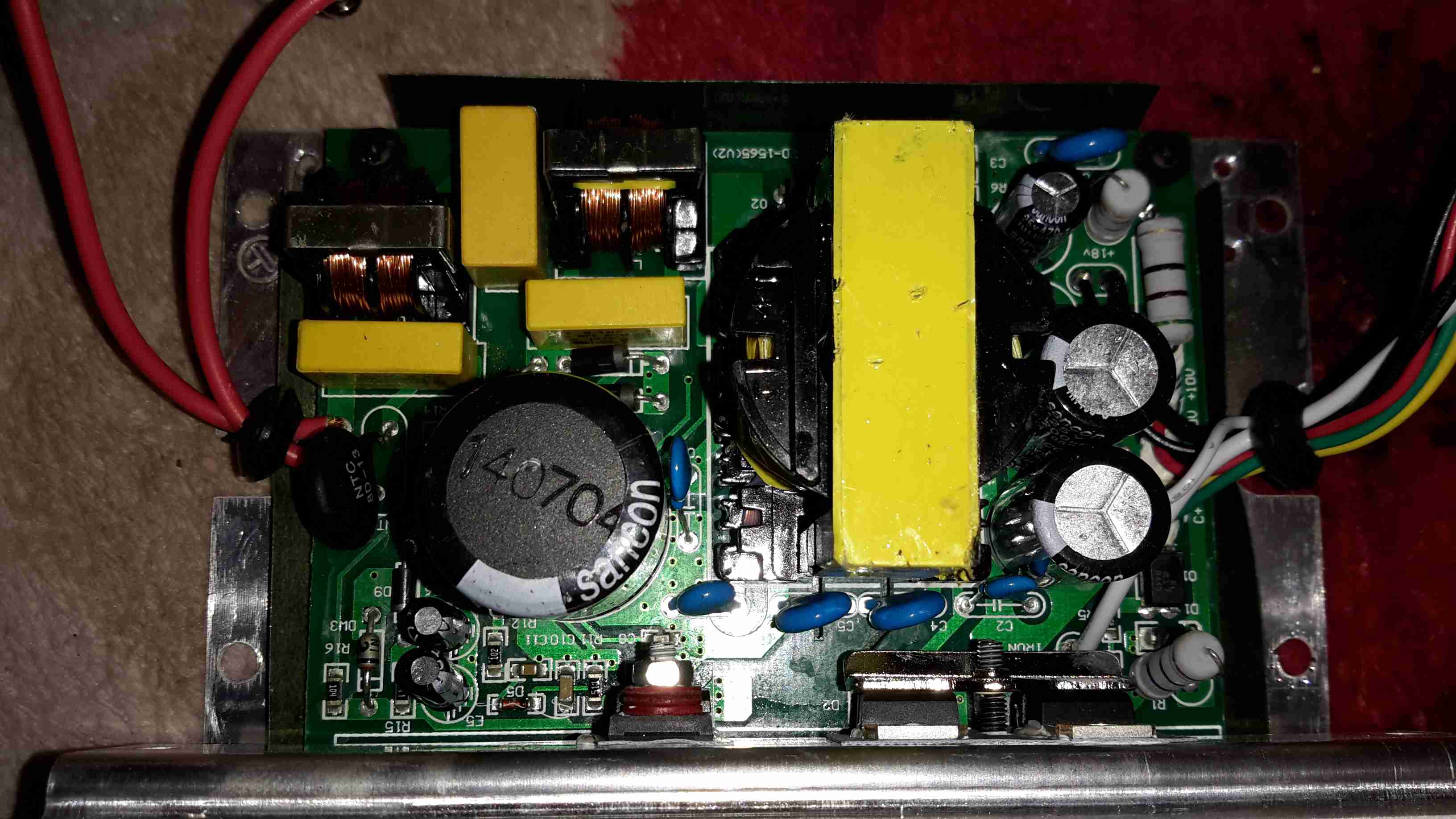
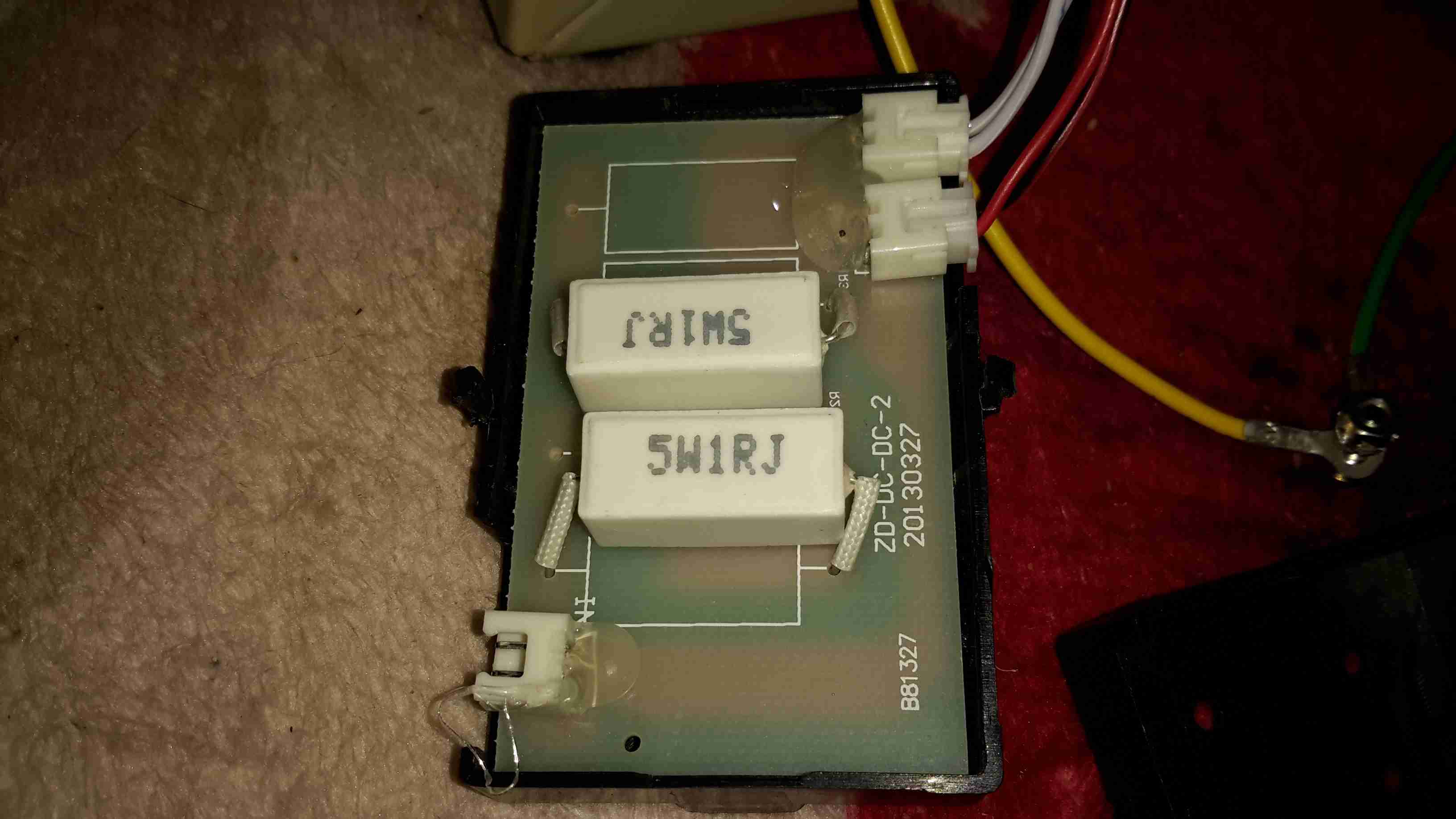
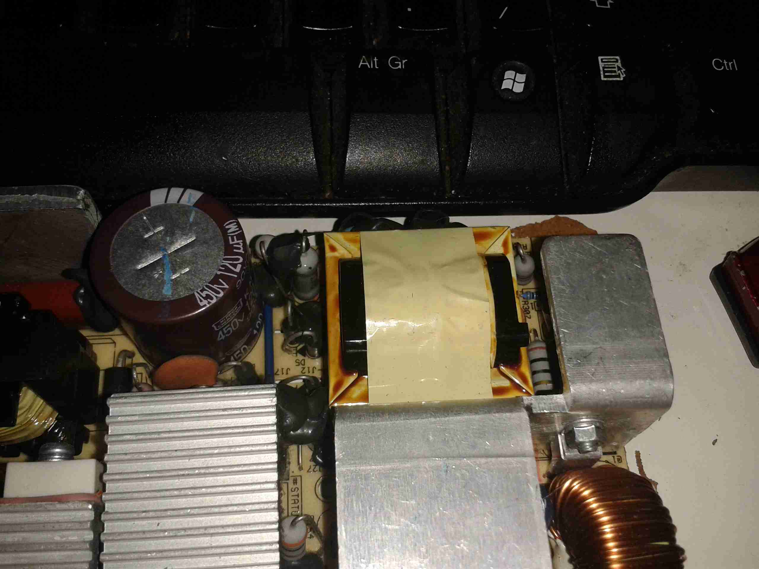
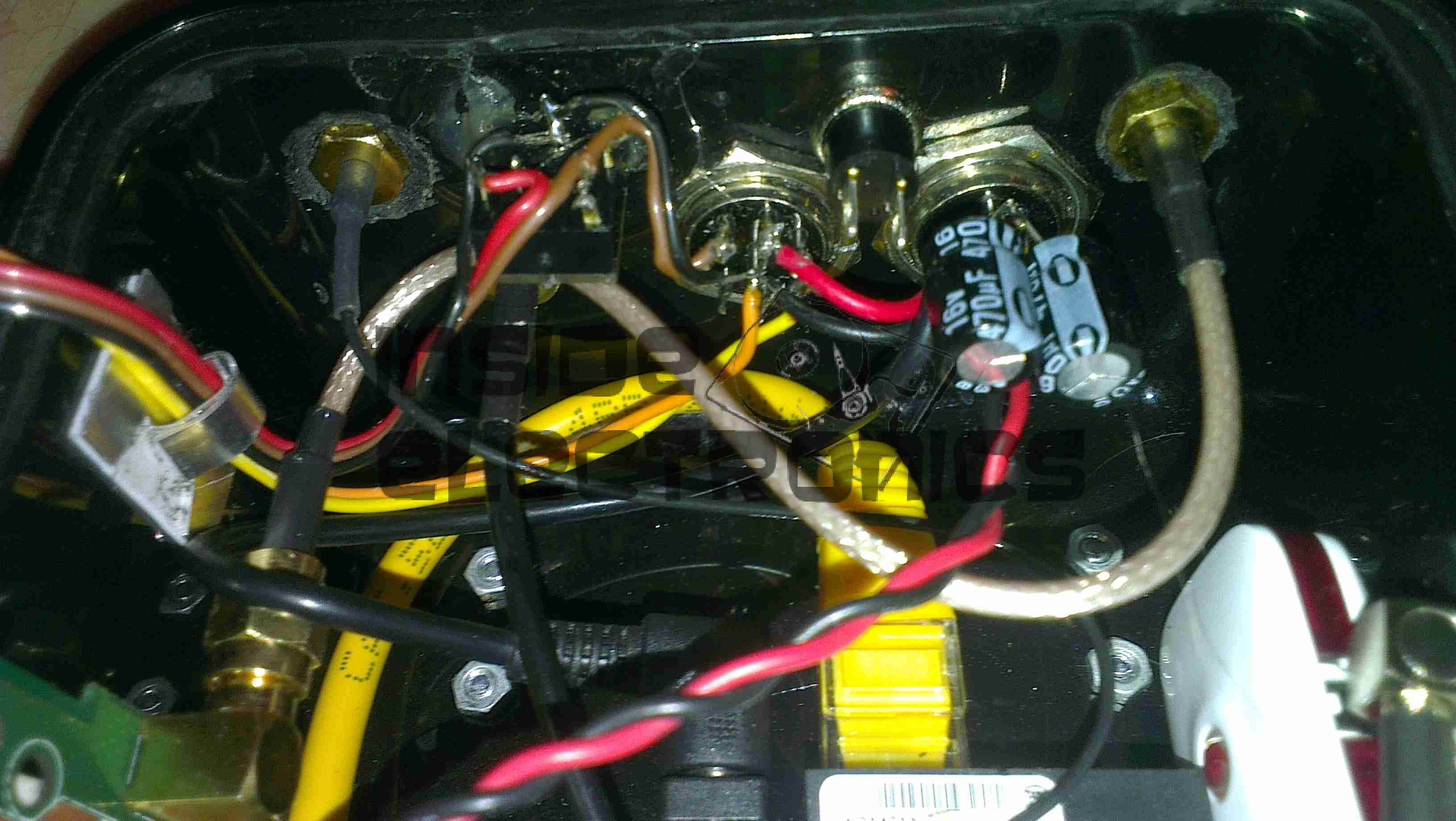
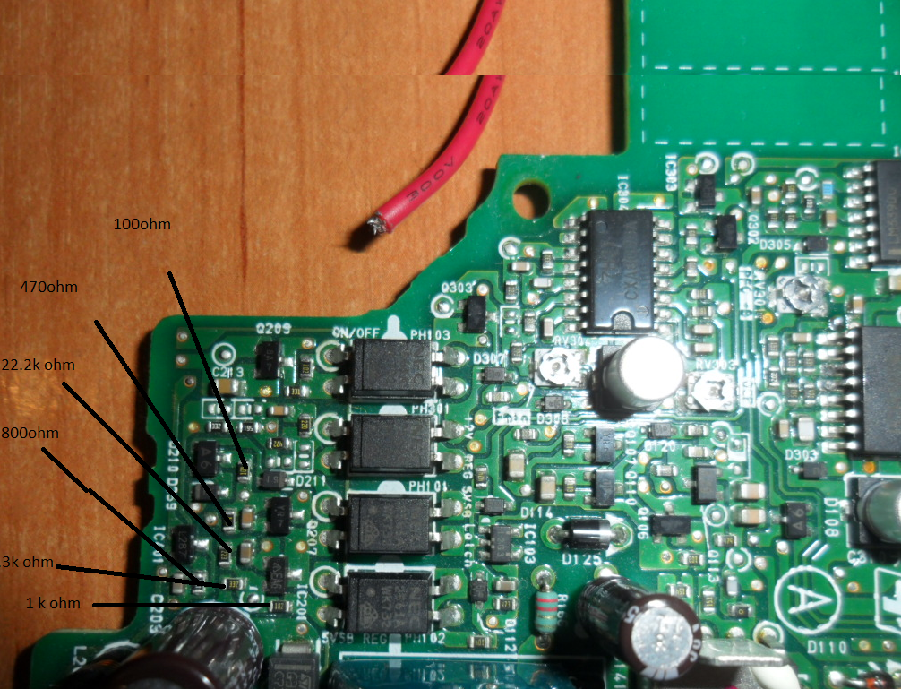
Here’s the regulator section of the PSU, with the resistors labelled. The one we’re after changing is the 800Ω one between pins 2 & 3 of the TS2431 shunt reference. It’s a very small 0402 size resistor, located right next to the filter electrolytic for the 5v standby supply circuit. A fine tip on the soldering iron is required to get this resistor removed.

Attachment Points
Attachment Points

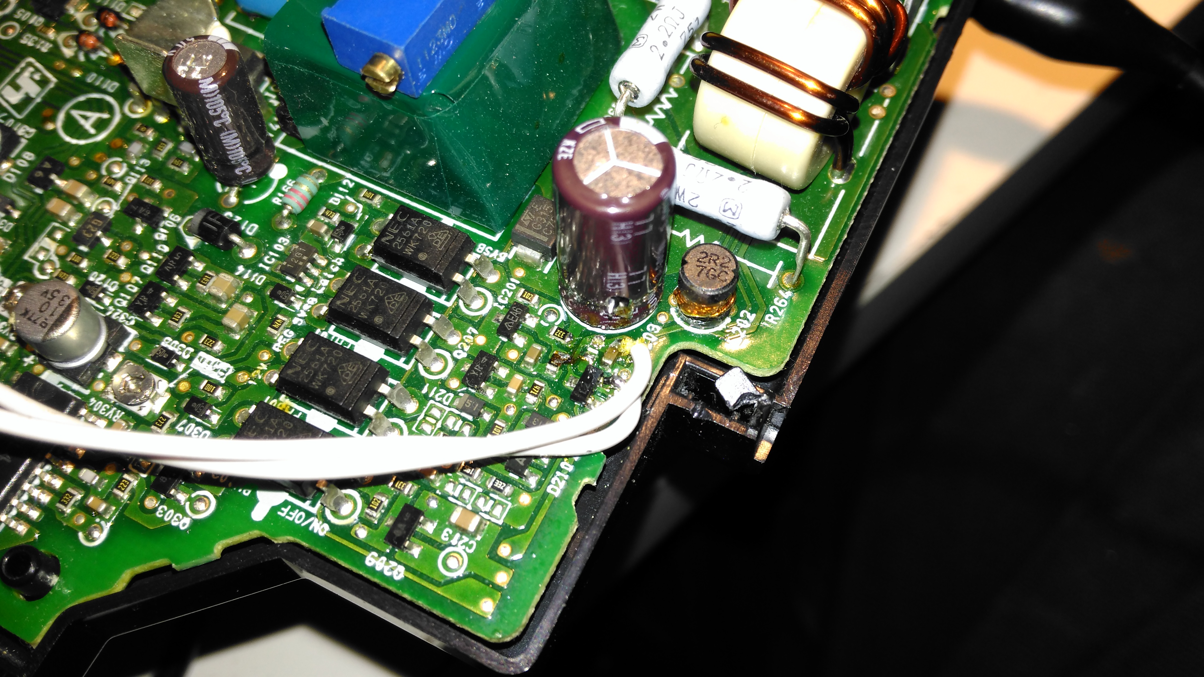
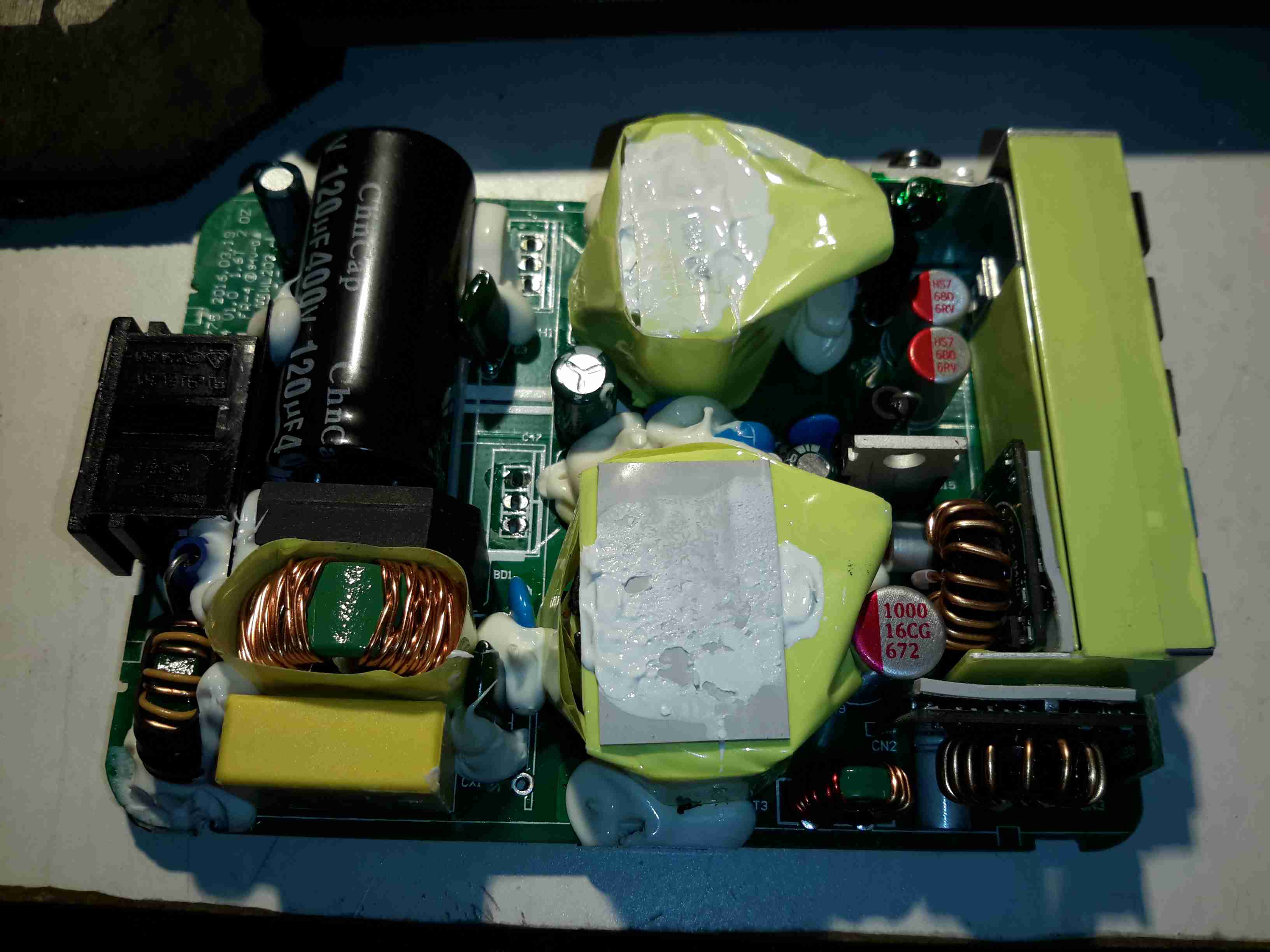
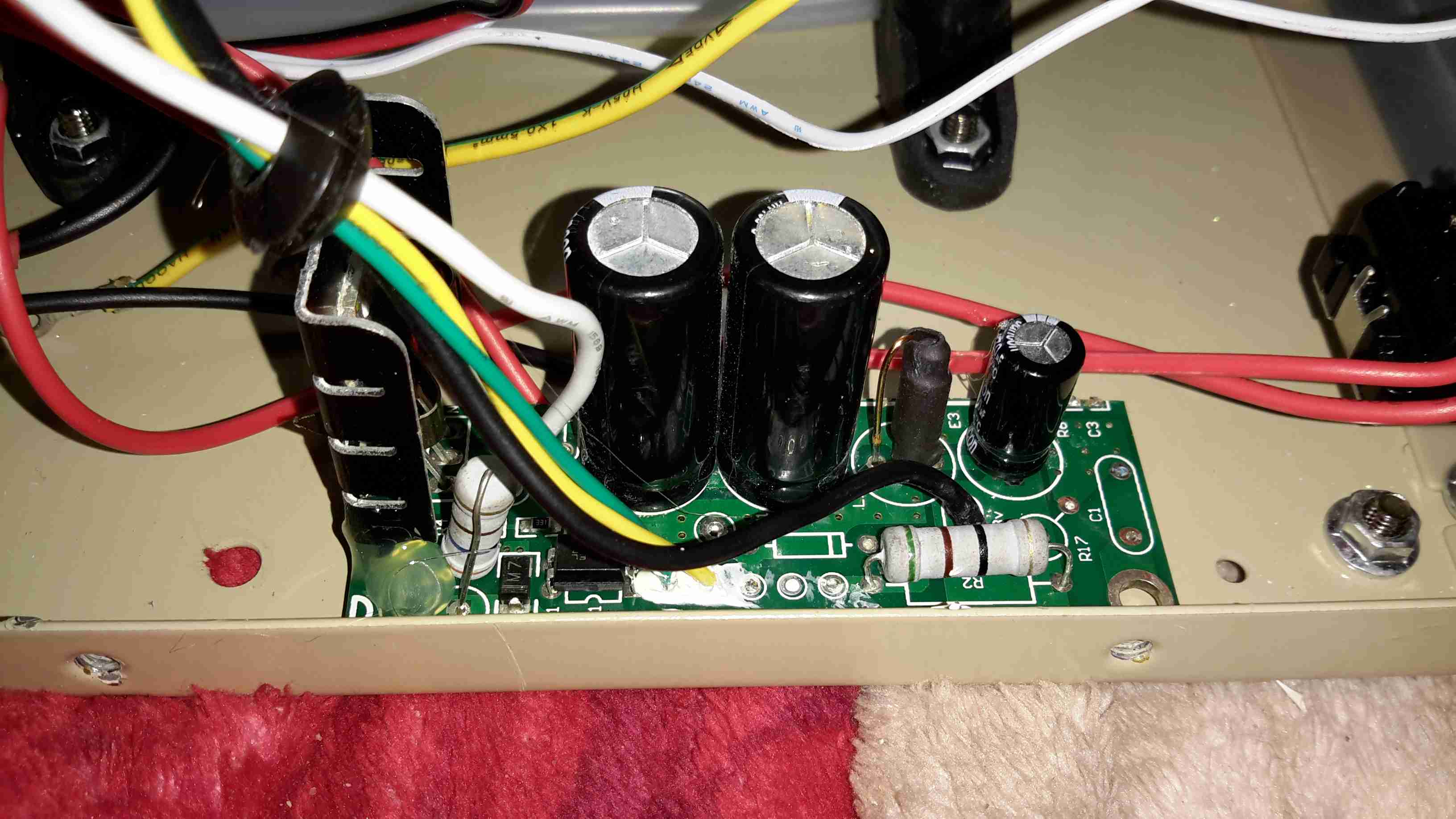
Once this resistor is removed from the circuit, a 1KΩ 18-turn potentiometer is fitted in it’s place, from the Anode (Pin 3) to the Ref. (Pin 2) pins of the TS2431 shunt reference. I initally set the potentiometer to be the same 800Ω as the factory set resistor, to make sure the supply would start up at a sensible voltage before I did the adjustment.

Potentiometer
Potentiometer

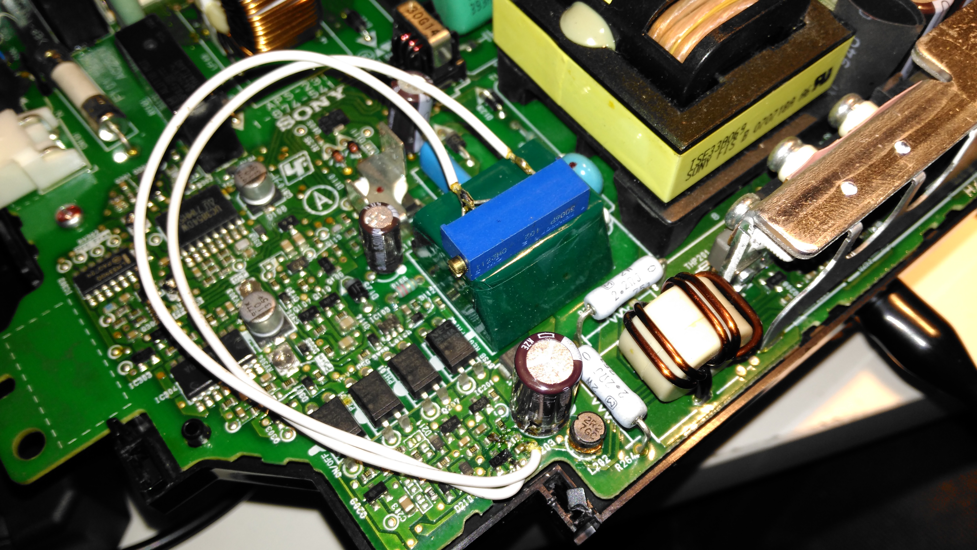
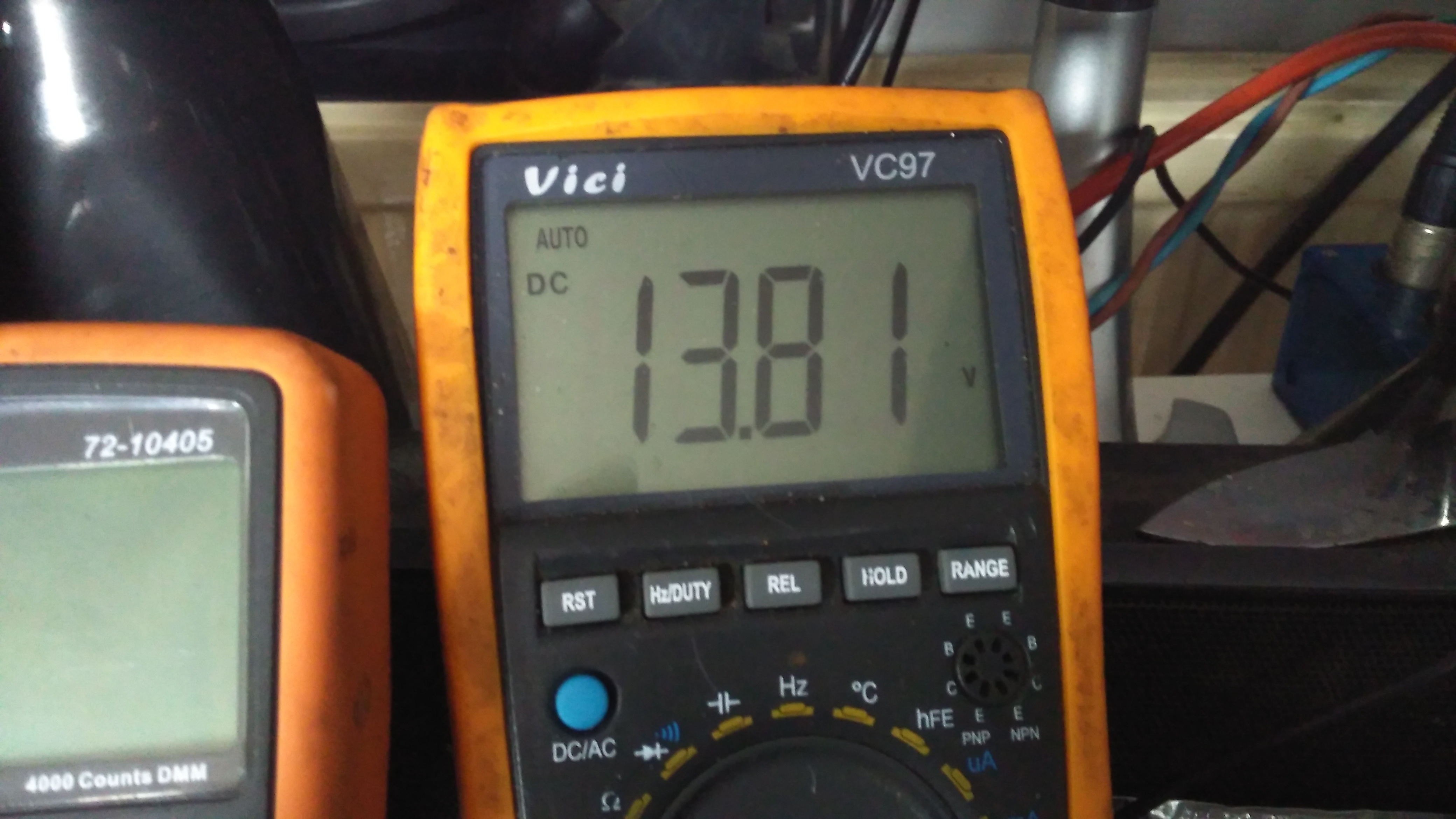
The pot is secured to the top of the standby supply transformer with a drop of CA glue to stop everything moving around. The supply can now be adjusted to a higher setpoint voltage – 13.8v is about the maxumum, as the OVP cuts the supply out at between 13.9v-14v.

Modded Voltage
Modded Voltage

After doing some testing at roughly 50% of the supply’s rated load, everything seems to be stable, and nothing is heating up more than I’d expect.

Posted on 3 Comments

Anker PowerPort Speed 5 USB Rapid Charger Teardown

Front
Front

Here’s a piece of tech that is growing all the more important in recent times, with devices with huge battery capacities, a quick charger. This unit supports Qualcomm’s Quick Charge 3 standard, where the device being charged can negotiate with the charger for a higher-power link, by increasing the bus voltage past the usual 5v.

Rear
Rear

The casing feels rather nice on this unit, sturdy & well designed. All the legends on the case are laser marked, apart from the front side logo which is part of the injection moulding.

Specifications
Specifications

The power capacity of this charger is pretty impressive, with outputs for QC3 from 3.6-6.5v at 3A, up to 12v 1.5A. Standard USB charging is limited at 4.8A for the other 3 ports.

Ports
Ports

The two of the 5 USB ports are colour coded blue on the QC3 ports. The other 3 are standard 5v ports, the only thing that doesn’t make sense in the ratings is the overall current rating of the 5v supply (4.8A), and the rated current of each of the ports (2.4A) – this is 7.2A total rather than 4.8A.

Top Removed
Top Removed

The casing is glued together at the seam, but it gave in to some percussive attack with a screwdriver handle. The inside of this supply is mostly hidden by the large heatspreader on the top.

Main PCB Bottom
Main PCB Bottom

This is a nicely designed board, the creepage distances are at least 8mm between the primary & secondary sides, the bottom also has a conformal coating, with extra silicone around the primary-side switching transistor pins, presumably to decrease the chances of the board flashing over between the close pins.
On the lower 3 USB ports can be seen the 3 SOT-23 USB charge control ICs. These are probably similar to the Texas Instruments TPS2514 controllers, which I’ve experimented with before, however I can’t read the numbers due to the conformal coating. The other semiconductors on this side of the board are part of the voltage feedback circuits for the SMPS. The 5v supply optocoupler is in the centre bottom of the board.

Heatsink Removed
Heatsink Removed

Desoldering the pair of primary side transistors allowed me to easily remove the heatspreader from the supply. There’s thermal pads & grease over everything to get rid of the heat. Here can be seen there are two transformers, forming completely separate supplies for the standard USB side of things & the QC3 side. Measuring the voltages on the main filter capacitors showed me the difference – the QC3 supply is held at 14.2v, and is managed through other circuits further on in the power chain. There’s plenty of mains filtering on the input, as well as common-mode chokes on the DC outputs before they reach the USB ports.

Quick Charge 3 DC-DC Converters

Here’s where the QC3 magic happens, a small DC-DC buck converter for each of the two ports. The data lines are also connected to these modules, so all the control logic is located on these too. The TO-220 device to the left is the main rectifier.

Posted on Leave a comment

Mercury 30A Ham Radio SMPS

Mercury 30A SMPS
Mercury 30A SMPS

After having a couple of the cheap Chinese PSUs fail on me in a rather spectacular fashion, I decided to splash on a more expensive name-brand PSU, since constantly replacing PSUs at £15 a piece is going to get old pretty fast. This is the 30A model from Mercury, which seems to be pretty well built. It’s also significantly more expensive at £80. Power output is via the beefy binding posts on the front panel. There isn’t any metering on board, this is something I’ll probably change once I’ve ascertained it’s reliability. This is also a fixed voltage supply, at 13.8v.

Rear Panel
Rear Panel

Not much on the rear panel, just the fuse & cooling fan. This isn’t temperature controlled, but it’s not loud. No IEC power socket here, the mains cable is hard wired.

Main Board
Main Board

Removing some spanner-type security screws reveals the power supply board itself. Everything on here is enormous to handle the 30A output current at 13.8v. The main primary side switching transistors are on the large silver heatsink in the centre of the board, feeding the huge ferrite transformer on the right.

Transformer
Transformer

The transformer’s low voltage output tap comes straight out instead of being on pins, due to the size of the winding cores. Four massive diodes are mounted on the black heatsinks for output rectification.


SMPS Controller
SMPS Controller

The supply is controlled via the jelly bean TL494 PWM controller IC. The multi-turn potentiometer doesn’t adjust the output voltage, more likely it adjusts the current limit.

Standby Supply
Standby Supply

Power to initially start the supply is provided by a small SMPS circuit, with a VIPer22A Low Power Primary Switcher & small transformer on the lower right. The transformer upper left is the base drive transformer for the main high power supply.

Posted on Leave a comment

Behringer DEQ2496 Mastering Processor

Bootscreen
Bootscreen

I was recently given this unit, along with another Behringer sound processor to repair, as the units were both displaying booting problems. This first one is a rather swish Mastering Processor, which has many features I’ll leave to Behringer to explain 😉

Input Board & Relays

All the inputs are on the back of this 19″ rackmount bit of kit, nothing much on this PCB other than the connectors & a couple of switching relays.

Main Processor PCB
Main Processor PCB

All the magic is done on the main processor PCB, which is host to 3 Analog Devices DSP processors:

ADSP-BF531 BlackFin DSP. This one is probably handling most of the audio processing, as it’s the most powerful DSP onboard at 600Mhz. There’s a ROM on board above this for the firmware & a single RAM chip. On the right are a pair of ADSP-21065  DSP processors at a lower clock rate of 66MHz. To the left is some glue logic to interface the user controls & dot-matrix LCD.

PSU Module
PSU Module

The PSU in this unit is a pretty standard looking SMPS, with some extra noise filtering & shielding. The main transformer is underneath the mu-metal shield in the centre of the board.

Posted on Leave a comment

eBay Flyback High Voltage PSU

Flyback PSU
Flyback PSU

I have found myself needing some more in the way of High Voltage supplies of late, with the acquisition of the new He-Ne laser tubes, so I went trawling eBay for something that would be suitable to run these tubes. (I currently only have a single He-Ne laser PSU brick, and they’re notoriously hard to find & rather expensive).
This supply is rated at 1kV-10kV output, at 35W power level. Unfortunately this supply isn’t capable of sustaining the discharge in a large He-Ne tube, the impedance of the supply is far too high. Still, it’s useful for other experiments.
The flyback-type transformer clearly isn’t a surplus device from CRT manufacture, as there are very few pins on the bottom, and none of them connect to the primary side. The primary is separately wound on the open leg of the ferrite core.

Drive Electronics
Drive Electronics

The drive electronics are pretty simple, there’s a controller IC (with the number scrubbed off – guessing it’s either a 556 dual timer or a SMPS controller), a pair of FDP8N50NZ MOSFETs driving the centre-tapped primary winding.
The drive MOSFETs aren’t anything special in this case: they’re rated at 500v 8A, 850mΩ on resistance. This high resistance does make them get rather hot even with no load on the output, so for high power use forced-air cooling from a fan would definitely be required.

Test Setup
Test Setup

Here’s the supply on test, I’ve got the scope probes connected to the gate resistors of the drive MOSFETs.

Waveforms
Waveforms

On the scope the primary switching waveforms can be seen. The FETs operate in push-pull mode, there’s a bit of a ring on the waveform, but they’re pretty nice square waves otherwise.

Arc
Arc

At maximum power on 12v input, about 25mm of gap is possible with an arc.

Posted on Leave a comment

Sky+ HD Set Top Box

Sky Box
Sky Box

Time for another teardown! I managed to fish this Sky+ box out of a skip, but to protect the guilty, all serial numbers have been removed.
These are pretty smart devices, with DVR capability on board.

Ports 1
Ports 1

There’s a lot of ports on these units, from RS-232 serial, POTS modem, eSATA, HDMI, USB, Ethernet, SCART, Optical, digital outputs & even composite video.

Ports 2
Ports 2
Ports 3
Ports 3
Top Panel
Top Panel

Removing the top plastic cover reveals the operation buttons & the built in WiFi adaptor, which is USB connected to the main logic board.

Front Panel
Front Panel

The PCB on the front of the chassis has all the indicators, and the IR Receiver for the remote.

Cover Removed
Cover Removed

Removing the top shield of the chassis reveals the innards. The PSU is on the top right, 500GB SATA disk drive in the bottom centre. The main logic PCB is top centre.

Logic PCB
Logic PCB

Here’s the main logic PCB. The massive heatsink in the middle is cooling the main SoC, below.

SoC
SoC

The main SoC in this unit is a Broadcom BCM7335 HD PVR Satellite System-On-Chip. It’s surrounded by it’s boot flash, a Spansion GL512P10FFCR1 512Mbit NOR device. It’s also got some DRAM around the left edge.

Smart Card Reader
Smart Card Reader

The smart card reader is on the PSU PCB, the controller here is an NXP TDA8024

PSU PCB
PSU PCB

The PSU itself is a pretty standard SMPS, so I won’t go too far into that particular bit. The logic PCB attaches to the large pin header on the left of the PSU, some of the analogue video outputs are also on this board.
There’s also a Microchip PIC16F726 microcontroller on this PCB, next to the pin header. Judging by the PCB traces, this handles everything on the user control panel.

Power Supplies
Power Supplies

Some local supplies are provided on the logic board for the main SoC, the IC in the centre here is an Allegro A92 DC-DC converter. I didn’t manage to find a datasheet for this one.

LNB Front End
LNB Front End

The RF front end for the satellite input is a Broadcom BCM3445 Low Noise Amplifier & Splitter, again not much info on this one.

RS232 Section
RS232 Section

The standard MAX232 is used for the serial interface. I imagine this is for diagnostics.

Modem
Modem

The POTS modem section is handled by a Si2457 System-Side device & Si3018 Line-Side device pair.

Posted on Leave a comment

De La Rue Coin Counting Machine

Here’s some teardown photos of an old De La Rue coin counter, used in businesses for rapid counting of change into large bags.

Mechanism
Mechanism

An overview of the whole mechanical system of the counter. Coins are loaded into the drum at the rear of the machine, which sorts them into a row for the rubber belt to pick up & run through the counter. The coin type to be sorted is selected by turning the control knobs on the right.
The control knobs adjust the width & height of the coin channel so only the correct sized coins will be counted.

PSU & Switching
PSU & Switching

The counter is driven by a basic AC induction motor, the motor power relay & reversing relay is on this PCB, along with the 5v switching supply for the main CPU board.
The SMPS on this board looks like a standard mains unit, but it’s got one big difference. Under the frame next to the main motor is a relatively large transformer, with a 35v output. This AC is fed into the SMPS section of the PSU board to be converted to 5v DC for the logic.
I’m not sure why it’s been done this way, and have never seen anything similar before.
The edge of the coin channel can be seen here, the black star wheel rotates when a coin passes & registers the count.

Controller PCB
Controller PCB

Here’s the main controller PCB, IC date codes put the unit to about 1995. The main CPU is a NEC UPD8049HC 8-bit micro, no flash or EEPROM on this old CPU, simply mask ROM. Coin readout is done on the 4 7-segment LED displays. Not much to this counter, it’s both electronically & mechanically simple.

Counter Sensor
Counter Sensor

Coin counting is done by the star wheel mentioned above, which drives the interrupter disc on this photo-gate. The solenoid locks the counter shaft to prevent over or under counting when a set number of coins is to be counted.

Motor Run Capacitor
Motor Run Capacitor

Under the frame, here on the left is the small induction motor, only 6W, 4-pole. The run cap for the motor is in the centre, and the 35v transformer is just visible behind it.

Main Motor Drive
Main Motor Drive

Main drive to the coin sorting mech is through rubber belts, and bevel gears drive the coin drum.

Posted on Leave a comment

Duratool ZD-915 12v Conversion

Inkeeping with everything else in my shack being low voltage operated, I had planned from the outset to convert the desoldering station to 12v operation. It turns out this has been the easiest tool to convert in my shack so far.

PSU Outputs
PSU Outputs

The factory SMPS is a fairly straightforward 18v 12A unit, with only a single small oddity: the desoldering gun’s heating element is controlled from inside the supply.

Iron MOSFET
Iron MOSFET

Next to the output rectifier on the heatsink is a large MOSFET, in this case a STP60NF06 from ST Micro. This is a fairly beefy FET at 60v & 60A capacity, RDS On of <0.016Ω.
This is driven via an opto-isolator from the main logic board. I’ve not yet looked at the waveform on the scope, but I suspect this is also being PWM’d to control temperature better when close to the set point.

Iron Element Controller

Rather than fire up the soldering iron & build a new element controller circuit (Lazy Mode™), I opted to take a saw to the original power supply. I cut the DC output section of the PCB off the rest of the supply & attached this piece back to the frame of the base unit. I also added a small heatsink to the MOSFET to make sure it stays cool.

12v Power Supply
12v Power Supply

Since the fan & vacuum pump are both already 12v rated, those are connected directly to the DC input socket, that I’ve installed in place of the original IEC mains socket. The 18v for the heating element is generated by a 10A DC-DC converter, again from eBay.

Oddly, the iron itself is rated at 24v 80W, but the factory supply is only rated to 18v. I’m not sure why they’ve derated the system, but as the station already draws up to 10A from a 13.8v supply, increasing the voltage any further would start giving my DC supplies a problem, so it can stay at 18v for now.

Posted on 3 Comments

Duratool ZD-915 Vacuum Desoldering Station Teardown

For a long time I’ve needed a decent vacuum desoldering tool, as I do much stripping of old PCBs for random parts.
Solder wick works well for most things, but it’s expensive & can be fiddly. It also doesn’t keep very long as the copper braid oxidises & after that point it never seems to work particularly well, even when soaked in fresh flux.

Desoldering Station
Desoldering Station

As usual eBay to the rescue! I managed to pick this one up for £80.

Vacuum Pump
Vacuum Pump

Removing the lid reveals the internals. Front & centre is the vacuum pump, with the mains supply behind it. There’s also a very noisy cooling fan at the back. Not sure why since the unit never gets warm enough to actually warrant a fan.

PSU
PSU

On the other side is the PSU. This is an 18v 12A rated SMPS, with a bit of custom electronics for controlling the iron element. Mounted to the back case is a small black box, more to come on this bit.

PSU Board
PSU Board

Cracking the case of the PSU reveals a pretty bog-standard SMPS, with a surprising amount of mains filtering for a Chinese supply. The DC outputs are on the right.

20160101_111613

From the rail markings, this is clearly designed to output some more voltage rails – possibly for other models of unit. In this case though, a single 18v rail is present. The iron’s element connects directly to the supply, controlled via an opto-isolated MOSFET.

Chinese Voltage Regulation

As both the fan & the vacuum pump motor are 12v devices, some provision had to be made to reduce the 18v from the power supply to a more reasonable value. Inside the black plastic box are a pair of 1Ω 5W power resistors, connected in series. The output from this connects to the fan & vacuum pump. Because cheap, obviously.

Controller
Controller

Finally, here’s the controller PCB, the main MCU is an 8081 derivative, with a Holtek HT1621B LCD controller for the front panel temperature readout. Iron temperature is achieved by a thermocouple embedded in the heater, I imagine the potentiometer on the left side of the PCB is for calibration.

Posted on Leave a comment

Rigol DS1054Z 12v Power Supply Noise Filtering

Since I fitted my scope with a SMPS based 12v input supply, there has been a noise problem on very low volts/div settings, this noise isn’t present on the mains supply, so I can only think it’s coming from the switching frequencies of the various DC-DC modules I’ve used.

Scope Ripple
Scope Ripple

Because of this I’ve designed a linear post-regulation stage for the supply, to remove the RFI from the DC rails.
This board takes the outputs from the DC-DC converters, removes all the noise & outputs clean DC onto the mainboard of the scope.

As the scope internally uses regulation to get the voltages lower, I’ve found that I don’t have to match the outputs of the mains supply exactly, for the +/-17.5v rails, 12v is perfectly fine instead.

Scope Linear PSU
Scope Linear PSU

Here’s the PCB layout, with the 6  common mode filters on the input (left), linear regulator ICs in the centre & the output filters on the right.

Scope Linear PSU
Scope Linear PSU

Here’s the schematic layout, as usual the Eagle Project files are in the link below, I’ll update when I have built the board & tested!

[download id=”5589″]

73s for now 🙂

Posted on 2 Comments

Rigol DS1054Z Power Supply Project

Since everything in my shack is run from 12v, I thought it would be handy to convert my new scope to 12v as well, as 99% of the places I find myself needing test gear are off grid, with no access to mains supplies.

Mains PSU
Mains PSU

Here’s the factory mains SMPS unit from the back of the scope. This is a nice multi-rail unit, with several different outputs, the table below details the wiring of the PSU.

Connector PinPCB PinSignalMeasured VoltageMainboardRectifier RatingWire Colour
51AC_TRIGN/AAC_TRIGN/ABROWN
22+9v_GNDN/AFAN --NAORANGE
113+9V10.16VFAN +2AWHITE
64+5V5.1V5V5A20ARED
135+5V5.1V5V5A20ARED
76GNDN/AGNDN/ABLACK
87GNDN/AGNDN/ABLACK
38+7.5V6.9V6.3V20AYELLOW
109+7.5V6.9V6.3V20AYELLOW
110GNDN/AGNDN/ABLACK
121117.5V17.51V17.5V2ABLUE
912-17.5V-17.36V-17.5V2AGREY
1413GNDN/AGNDN/ABLACK
414-7.5V-6.84V-7.5V2AGREEN

The only feature I will lose if I make this switch is AC line triggering, but I never use that anyway, so it’s not a big issue for me.

The connector used by Rigol to connect to the mainboard is a Molex Mini Fit Jr. Series 14-way type.

Since I have been able to locate the connector, the plan is to design a replacement low voltage supply unit for the scope, with the same footprint as the original AC mains supply. This will allow me to do a direct swap without causing any damage or modifying the original supply.
This method will allow me to swap the 240v supply back into the scope if I ever come to need it.

I’m planning to use the LTC3863 DC-DC Controller from Linear Tech to generate the negative rails, this will go down to -150v on the output, so it’s pretty much perfect to generate them.

PSU Output Side
PSU Output Side

Here’s the output side of the mains PSU, it has a lot of filtering on the output rails, the two TO220 devices are the output rectifiers for the +5v & +7.5v rails, these are rated at 20A, 60V.

PCB Bottom
PCB Bottom

Here’s the bottom side of the PCB. It’s a really nicely designed PSU, massive isolation gap, spark gaps on the primary side & good filtering. The output side on the left has the rectifier diodes for the other voltage rails, these are only 2A rated, so designing the inverting supply to generate the negative rails will be pretty easy.

From looking at the PCB markings on both the mainboard & the PSU, the +9v rail seems to be used to drive the fan, both silkscreen markings indicate this.
The voltages marked on the PSU & the mainboard connector don’t quite match up though, there’s a small variation in the stated voltage between the two. This is most likely because all of the regulation of the supplies seems to be done on the mainboard, there are several linear regulators, and a few DC-DC switchers. Providing that the replacement supply isn’t noisy it should work fine.

This is backed up by the fact that the mains PSU only seems to regulate the +5v rail – on measuring the rails that’s the only one that’s close to spec.

Mainboard Power
Mainboard Power

Here’s the mainboard power connector, with it’s silkscreen labelling on the pins. (Very useful). As can be seen here, there’s at least 5 regulators, of both switching & linear types here, generating both positive & negative rails.


More to come when I have some components!

73s for now 🙂

Posted on Leave a comment

Samsung ETA-U90UWE Adaptor Failure

Here’s an odd & sudden failure, the power adaptor for a Samsung device. It’s been working for months & on being plugged into the mains today the magic blue smoke escaped.

Samsung Charger
Samsung Charger

It’s one of their 2A models, for charging bigger devices like tablets.

Flash Burn
Flash Burn

Strangely for one of these chargers, no glue is used to hold it together – just clips. This made disassembly for inspection much easier. Evidence of a rather violent component failure is visible inside the back casing.

PCB
PCB

Here’s the charger PCB removed from the casing. As to be expected from Samsung, it’s a high quality unit, with all the features of a well designed SMPS.

PCB Reverse
PCB Reverse

However, on turning the board over, the blown component is easily visible. It’s the main SMPS controller IC, with a massive hole blown in the top. The on board fuse has also blown open, but it obviously didn’t operate fast enough to save the circuit from further damage!


Posted on Leave a comment

Chinese 12v 10A Power Brick Analysis

I recently ordered a PSU to run one of the TVs I converted to 12v operation, and being an older TV, it’s a fairly heavy load at 6.5A. eBay to the rescue again, with a cheap 10A rated supply.

Power Brick
Power Brick

Like all similar supplies these days, it’s a SMPS unit, and feels suspiciously light for it’s power rating.

Cover Removed
Cover Removed

Luckily this one is easy to get into, no ultrasonic welding on the case, just clips. Here’s the top cover removed, big alloy plate between the heatsinks.

PCB
PCB

The top heatsink plate was glued to the top of the transformer with silicone, some gentle prying released it. From the top, things don’t look too bad. There’s some filtering on the mains input & it’s even fused!

Primary Side
Primary Side

Here’s a closeup of the primary side of the PSU, the main DC bus capacitor is a Nichicon one, but it’s clearly been recovered from another device, look at the different glue on the end!
it’s also flapping about in the breeze, the squirt of silicone they’ve put on does nothing to stop movement.
Also here is the mains input fuse, filter capacitor & common mode choke. At least there is some filtering!

The main control IC is a UC3843B High Performance Current Mode PWM Controller, operating at a switching frequency of 250kHz.
The main switching transistor is visible at the bottom left corner, attached to the heatsink.

Secondary Side
Secondary Side

Here’s the secondary side of the supply. The transformer itself is OK, nice heavy windings on the output to suit the high current.
It’s using proper opto-isolated feedback for voltage regulation, with a TL431 reference IC.
The output diodes are attached to the heatsink at the top of the photo, I couldn’t read any numbers on those parts.

The output filter capacitors are low quality, only time will tell if they survive. I’ll put the supply under full load & see what the temperature rise is inside the casing.

PCB Bottom
PCB Bottom

On the bottom of the PCB things get a little more dire. There isn’t really much of an isolation gap between the primary & secondary sides, and there’s a track joining the output negative with mains earth, which gets to within 2mm of the live mains input!

As with all these cheapo supplies, there’s good points & bad points, I will update when I’ve had a chance to put the supply under full load for a while & see if it explodes!


Posted on Leave a comment

Lethal Chinese Mains Adaptors

With every piece of Chinese electronics I obtain, mainly Baofeng radios, they come with a Europlug-type power adaptor, and a universal plug adaptor for the mains.

The charger units aren’t too bad, there’s a fair amount of isolation between the primary & secondary, and even though they’re very simple & cheap, I can’t see any immediate safety problems with them.

The plug adaptors, however, are a different matter. These things are utterly lethal!

Baofeng PSU
Baofeng PSU

Here’s the inside of the PSU. It’s just a very simple SMPS, giving an output of 10v 500mA. The fuse is actually a fusible resistor.

PCB Reverse
PCB Reverse

Here’s the back of the PCB with the SMPS control IC. I can’t find any English datasheets for this part unfortunately.

Universal Travel Adaptor

Here’s the dangerous adaptor. There’s no safety shield, so the live parts are exposed.

Internals
Internals

Here’s the adaptor split apart. The output contacts are on the left, and rely just on pressure to make contact with the brass screws on the mains input pins to provide power.
This is a very poor way to get a connection, a dirty or worn contact here would create a lot of heat if any significant power is pulled through, and could quite possibly result in a fire.

Not surprisingly, I bin these things as soon as I open the box, and charge all my radios with a 12v charging system.

Posted on 1 Comment

Cisco PSU Hack & Switched Mode PSU Background

Recently I decommissioned some networking equipment, and discovered the power supplies in some switches were single rail 12v types, with a rather high power rating. I figured these would be very good for powering my Ham radio gear.

They’re high quality Delta Electronics DPSN-150BP units, rated at a maximum power output of 156W.

Label
Label

These supplies have an adjustment pot for the output voltage regulation, but unfortunately it just didn’t have quite enough range to get from 12.0v to 13.8v. The highest they would go was ~13.04v.

After taking a look at the regulator circuit, I discovered  I could further adjust the output voltage by changing a single resistor to a slightly lower value.

Firstly though, a little background on how switched mode power supplies operate & regulate their output voltage.

SMPS
SMPS

Here’s the supply. It’s mostly heatsink, to cool the large power switching transistors.

The first thing a SMPS does, is to rectify the incoming mains AC with a bridge rectifier. This is then smoothed by a large electrolytic capacitor, to provide a main DC rail of +340v DC (when on a 240v AC supply).

Mains Input
Mains Input

Above is the mains input section of the PSU, with a large common-mode choke on the left, bridge rectifier in the centre, and the large filter capacitor on the right. These can store a lot of energy when disconnected from the mains, and while they should have a discharge resistor fitted to safely drain the stored energy, they aren’t to be relied on for safety!

Once the supply has it’s main high voltage DC rail, this is switched into the main transformer by a pair of very large transistors – these are hidden from view on the large silver heatsinks at the bottom of the image. These transistors are themselves driven with a control IC, in the case of this supply, it’s a UC3844B. This IC is hidden under the large heatsink, but is just visible in the below photo. (IC5).

Control IC
Control IC
Main Switching Transformer

Here’s the main switching transformer, these can be much smaller than a conventional transformer due to the high frequencies used. This supply operates at 500kHz.
After the main transformer, the output is rectified by a pair of Schottky diodes, which are attached to the smaller heatsink visible below the transformer, before being fed through a large toroidal inductor & the output filter capacitors.
All this filtering on both the input & the output is required to stop these supplies from radiating their operating frequency as RF – a lot of cheap Chinese switching supplies forego this filtering & as a result are extremely noisy.

After all this filtering the DC appears at the output as usable power.

Getting back to regulation, these supplies read the voltage with a resistor divider & feed it back to the mains side control IC, through an opto-isolator. (Below).

Feedback Loop
Feedback Loop

The opto isolators are the black devices at the front with 4 pins.

Regulator Adjustment

For a more in-depth look at the inner workings of SMPS units, there’s a good article over on Hardware Secrets.

My modification is simple. Replacing R306 (just below the white potentiometer in the photo), with a slightly smaller resistor value, of 2.2KΩ down from 2.37KΩ, allows the voltage to be pulled lower on the regulator. This fools the unit into applying more drive to the main transformer, and the output voltage rises.

It’s important to note that making too drastic a change to these supplies is likely to result in the output filter capacitors turning into grenades due to overvoltage. The very small change in value only allows the voltage to rise to 13.95v max on the adjuster. This is well within the rating of 16v on the output caps.

Now the voltage has been sucessfully modified, a new case is on the way to shield fingers from the mains. With the addition of a couple of panel meters & output terminals, these supplies will make great additions to my shack.

More to come on the final build soon!

Posted on Leave a comment

AD9850 VFO Board

Continuing from my previous post where I published an Eagle design layout for AD7C‘s Arduino powered VFO, here is a completed board.

I have made some alterations to the design since posting, which are reflected in the artwork download in that post, mainly due to Eagle having a slight psychotic episode making me ground one of the display control signals!

AD9850 VFO
AD9850 VFO

The amplifier section is unpopulated & bypassed as I was getting some bad distortion effects from that section, some more work is needed there.
The Arduino Pro Mini is situated under the display, and the 5v rail is provided by the LM7805 on the lower left corner.

Current draw at 12v input is 150mA, for a power of 1.8W total. About 1W of this is dissipated in the LM7805 regulator, so I have also done a layout with an LM2574 Switching Regulator.
The SMPS version should draw a lot let power, as less is being dissipated in the power supply, but this version is more complex.

DDS VFO-SMPS
DDS VFO-SMPS

Here the SMPS circuit can be seen on the left hand side of the board, completely replacing the linear regulator.
I have not yet built this design, so I don’t know what kind of effect this will have on the output signal, versus the linear regulator. I have a feeling that the switching frequency of the LM2574 (52kHz) might produce some interference on the output of the DDS module. However I have designed this section to the standards in the datasheet, so this should be minimal.

Nevertheless this version is included in the Downloads section at the bottom of this post.

The output coupled through a 100nF capacitor is very clean, as can be seen below, outputting a 1kHz signal. Oscilloscope scale is 0.5ms/div & 1V/div.

VFO Output
VFO Output (Mucky ‘Scope)
Scope Connected
Scope Connected


Thanks again to Rich over at AD7C for the very useful tool design!

Linked below is the Eagle design files for this project, along with my libraries used to create it.

[download id=”5571″]

[download id=”5573″]

[download id=”5575″]

Posted on Leave a comment

Potentially Lethal Clone Apple Charger

Charger
Charger

I received this USB supply with a laser module from China that I purchased on eBay. I have heard of these nasty copies of Apple chargers going around, but I’d never received one this bad with a piece of Chinese electronics.

Label
Label

Model No. A1265, so definitely an Apple clone. Apparently capable of +5v DC 1A output. Notice the American NEMA pins. This wouldn’t have been any use to me in the first instance since I am resident in the UK & our mains plugs are significantly different, not to mention significantly safer.

Manufacturer is marked as Flextronics.

Top Of Boards
Top Of Boards

Here is the charger disassembled. Inside the case these two boards are folded together, creating an alarmingly small isolation gap between the mains side of the supply & the 5v output. Both the low voltage output & the feedback loop for the supply runs over the 4-core ribbon cable.
The mains wiring from the board is as thin as hair, insulation included, so there is a big possibility of shorts all over the place from this part of the circuit alone.

Bottom Of Boards
Bottom Of Boards

Bottom of the PCB assemblies. Good luck finding any creepage distance here. There simply isn’t any at all. traces on the +350v DC rail on the mains side of the transformer are no more than 1mm away from the supposedly isolated low voltage side.

Plugging one of these devices into anything is just asking for electrocution.


Posted on Leave a comment

Wearable Raspberry Pi – Some Adjustments

USB Hub
USB Hub

As the first USB hub I was using was certainly not stable – it would not enumerate between boots & to get it working again would require waiting around 12 hours before applying power, it has been replaced. This is a cheapie eBay USB hub, of the type shown below.

These hubs are fantastic for hobbyists, as the connections for power & data are broken out on the internal PCB into a very convenient row of pads, perfect for integration into many projects.

Breakout Hub
Breakout Hub

I now have two internal spare USB ports, for the inbuilt keyboard/mouse receiver & the GPS receiver I plan to integrate into the build.

These hubs are also made in 7-port versions, however I am not sure if these have the same kind of breakout board internally. As they have the same cable layout, I would assume so.


Connector Panel
Connector Panel

Here is a closeup of the back of the connectors, showing a couple of additions.

I have added a pair of 470µF capacitors across the power rails, to further smooth out the ripple in the switching power supply, as I was having noise issues on the display.

Also, there is a new reset button added between the main interface connectors, which will be wired into the pair of pads that the Raspberry Pi has to reset the CPU.
This can be used as a power switch in the event the Pi is powered down when not in use & also to reset the unit if it becomes unresponsive.


Posted on Leave a comment

Wearable Raspberry Pi Part 2.5 – Battery Pack PCM

Battery PCM
Battery PCM

The final part for the battery pack has finally arrived, the PCM boards. These modules protect the cells by cutting off the power at overcharge, undercharge & overcurrent. Each cell is connected individually on the right, 12v power appears on the left connections. These modules also ensure that all the cells in the pack are balanced.


Posted on Leave a comment

Wearable Raspberry Pi SMPS Modifications

SMPS Mods
SMPS Mods

A few modifications were required to the SMPS modules to make the power rails stable enough to run the Pi & it’s monitor. Without these the rails were so noisy that instability was being caused.

I have replaced the 100µF output capacitors & replaced them with 35v 4700µF caps. This provides a much lower output ripple.

There are also heatsinks attached to the converter ICs to help spread the heat.

Posted on Leave a comment

DIY Valve Amplifier – Part 1 – Amplifier Section

Components
Components

Here are a few details of a valve amplifier I am building, using the valve related parts from a 1960’s reel to reel tape recorder.

This amplifier is based on an a Mullard ECL82 triode/pentode valve, with an EM84 magic eye tube for level indication.

Beginnings Of The Amplifier

Here the first components are being soldered to the tags on the valve holder, there are so few components that a PCB is not required, everything can be rats-nested onto the valve holders.

Progress
Progress

Progressing with the amplifier section componentry, all resistors are either 1/2W or 2W.

Valve Sockets Fitted

Here the valve holders have been fitted, along with the output transformer, DC smoothing capacitor & the filament wiring, into the top of the plastic housing. At this point all the components that complete the amplifier section are soldered to the bottom of the right hand valve holder.

Wiring
Wiring

Starting the wiring between the valves & the power supply components. The volume control pot is fitted between the valve holders.

Valves Test Fit
Valves Test Fit

The valves here are test fitted into their sockets, the aluminium can at the back is a triple 32uF 250v electrolytic capacitor for smoothing the B+ rail.

Amplifier Section First Test

First test of the amplifier, with the speaker from the 1960’s tape recorder from which the valves came from. the 200v DC B+ supply & the 6.3v AC filament supply is derived from the mains transformer in the background.

Magic Eye Tube Added

Here the magic eye tube has been fitted & is getting it’s initial tuning to the amplifier section. This requires selecting combinations of anode & grid resistors to set the gap between the bars while at no signal & picking a coupling RC network to give the desired response curve.

Final Test
Final Test

Here both valves are fitted & the unit is sitting on it’s case for final audio testing. the cathodes of the ECL82 can be clearly seen glowing dull red here.


In the final section, I will build a SMPS power supply into the unit to allow it to be powered from a single 12v DC power supply.