Posted on Leave a comment

Etching PCBs With Dry Film Photoresist

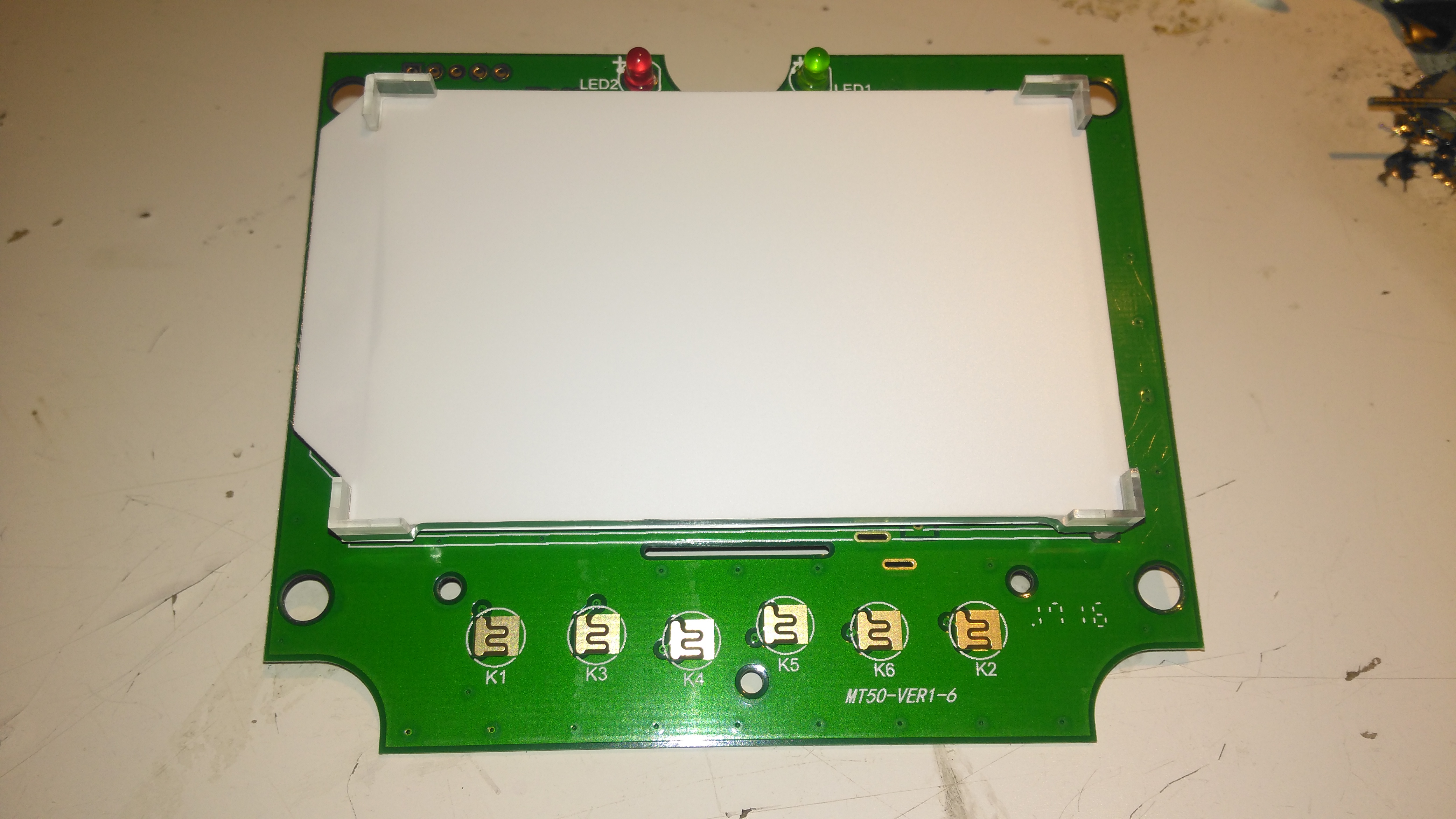
Since I do my own PCBs on a somewhat regular basis, I decided it was time to move to a more professional method to etch my boards. I have been using the cheap toner transfer method, using special yellow coated paper from China. (I think it’s coated in wax, or some plastic film).

The toner transfer paper does usually work quite well, but I’ve had many issues with pinholes in the transfer, which cause the etched tracks to look horrid, (not to mention the potential for breaks & reduced current capacity), and the toner not transferring properly at all, to issues with the paper permanently fusing to the copper instead of just transferring the toner.

BigClive has done a couple of fairly comprehensive videos on the dry film photoresist available from AliExpress & eBay. This stuff is used similarly to the toner transfer method, in that the film is fused to the board with heat, but then things diverge. It’s supplied either in cut sheets, or by the roll. I ordered a full roll to avoid the issues I’ve heard of when the stuff is folded in the post – once it’s creased, it’s totally useless. The dry film itself is a gel sandwiched between two protective plastic film sheets, and bonds to the board with the application of heat from a laminator.

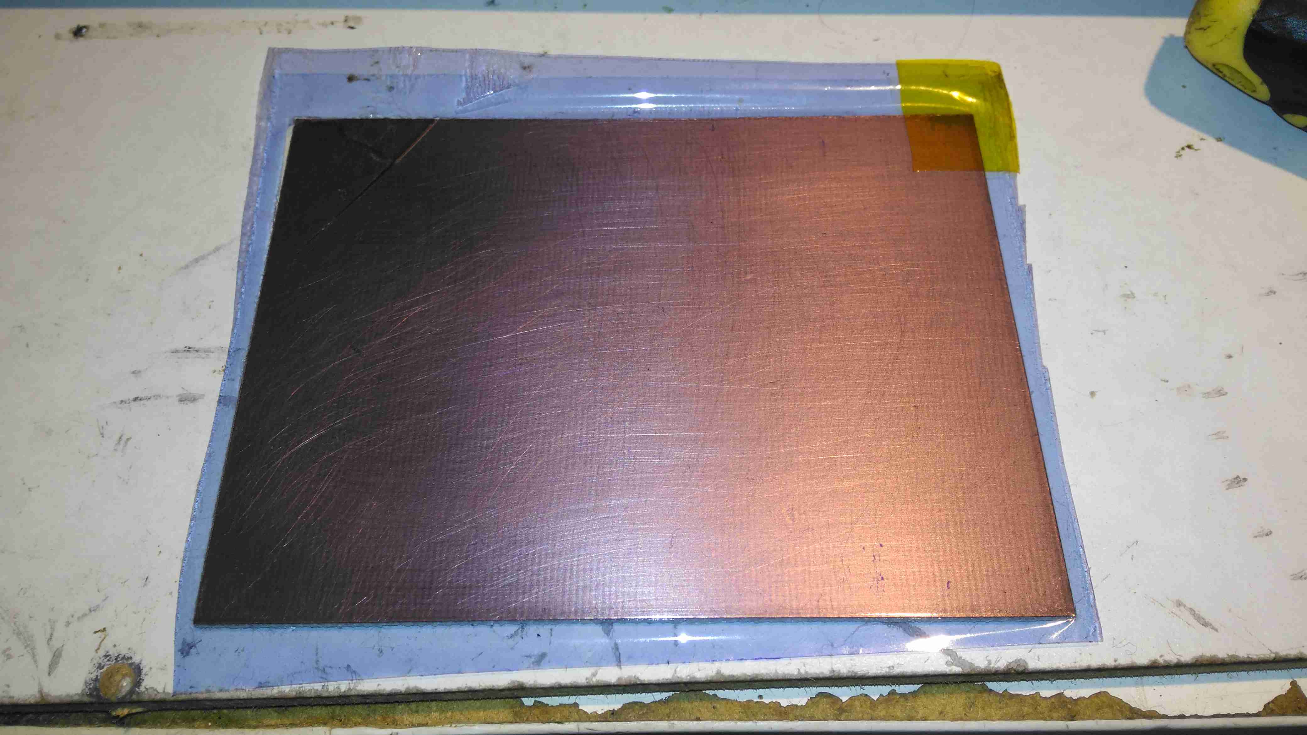
The board is first cleaned with scotchbrite pad & soap to remove any tarnish & oil from the copper.

Dry Film
Dry Film

Once the board has been cleaned, one side of the backing film is removed from the gel with adhesive tape, and the dry film is placed on the board while still wet. This stops the film from sticking immediately to the clean copper, one edge is pressed down, and it’s then fed through a modified laminator:

Modified Laminator
Modified Laminator

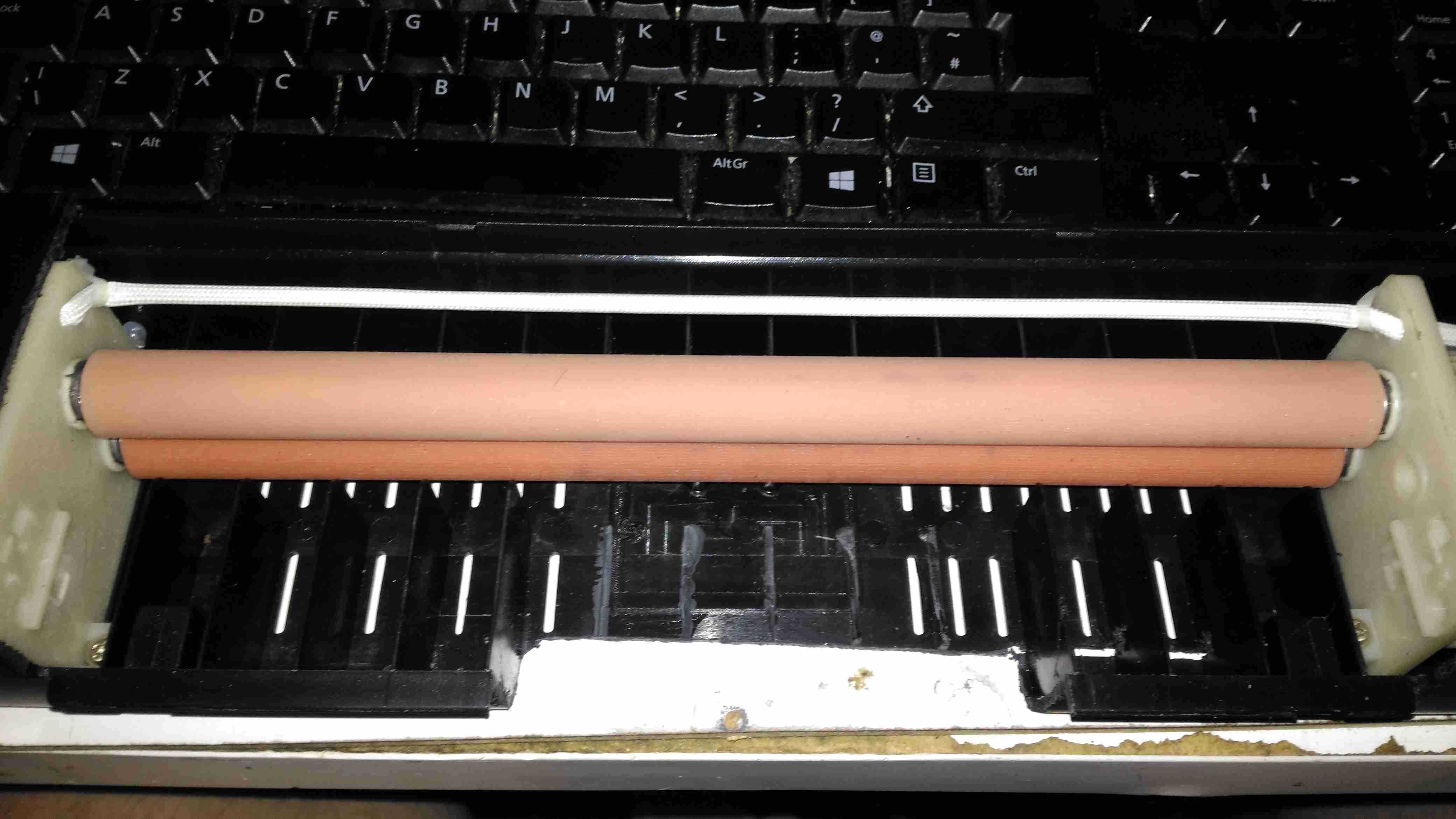
I’ve cut away most of the plastic covering the hot rollers, as constant jamming was an issue with this cheapo unit. All the mains power is safely tucked away under some remaining plastic cover at the end. The board with it’s covering of dry film is fed into the laminator – the edge that was pressed down first. This allows the laminator to squeeze out any remaining water & air bubbles from between the two so no creases or blisters form.

After Lamination
After Lamination

Once the board has been run through the laminator about 6 times, (enough to get it very hot to the touch), the film is totally bonded to the copper. The top film is left in place to protect the UV sensitive layer during expsure.

Photomask
Photomask

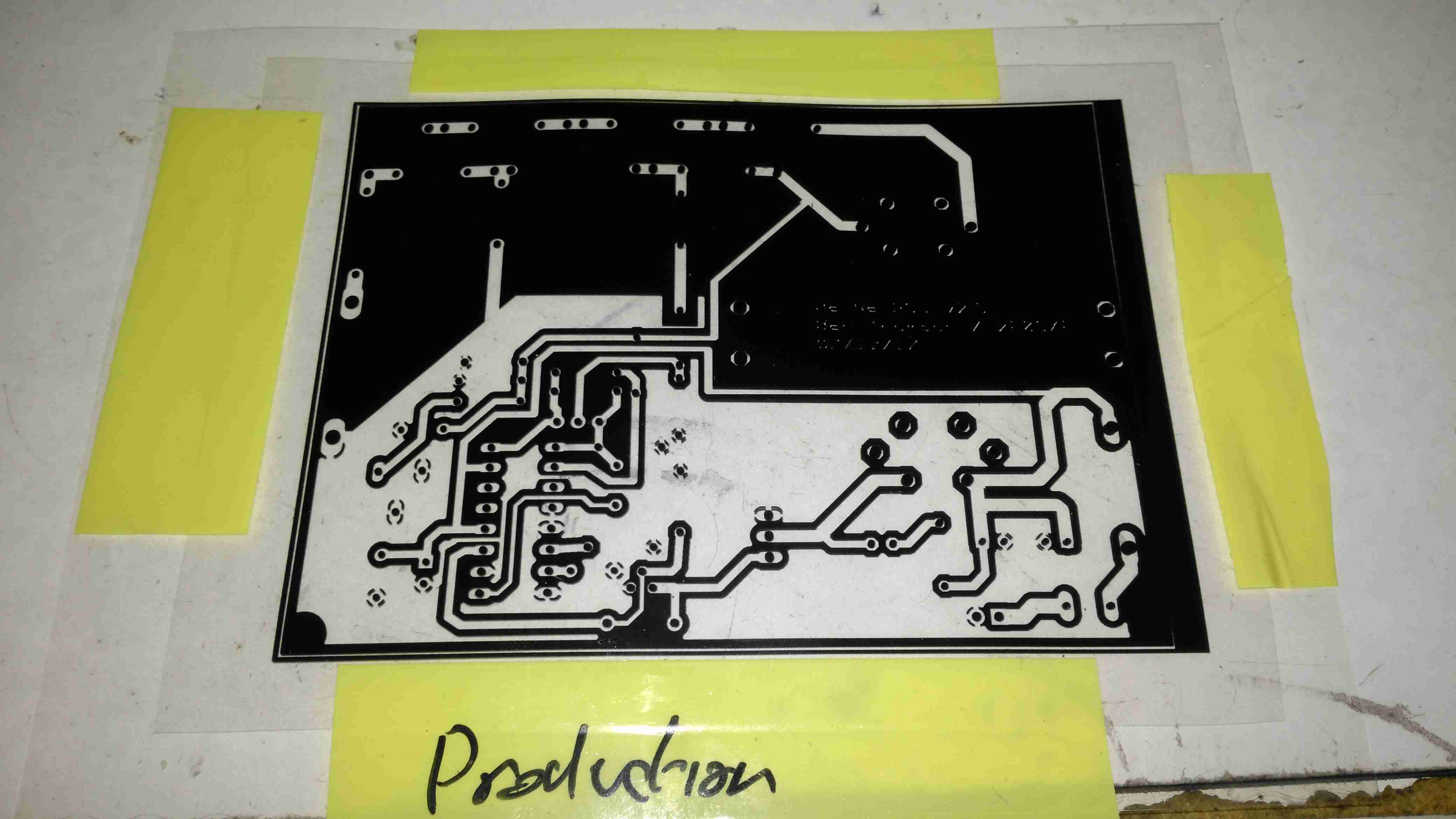
The exposure mask is laser printed onto OHP transparencies, in this case I’ve found I need to use two copies overlaid to get enough opacity in the black toner sections to block the UV light. Some touching up with a Sharpie is also easy to do if there are any weak spots in the toner coverage. This film is negative type – All the black areas will be unexposed and washed off in the developer tank. I also found I had to be fairly generous with track spacing, using too small lines just causes issues with the UV curing bits of film it isn’t supposed to.

Exposing The PCB
Exposing The PCB

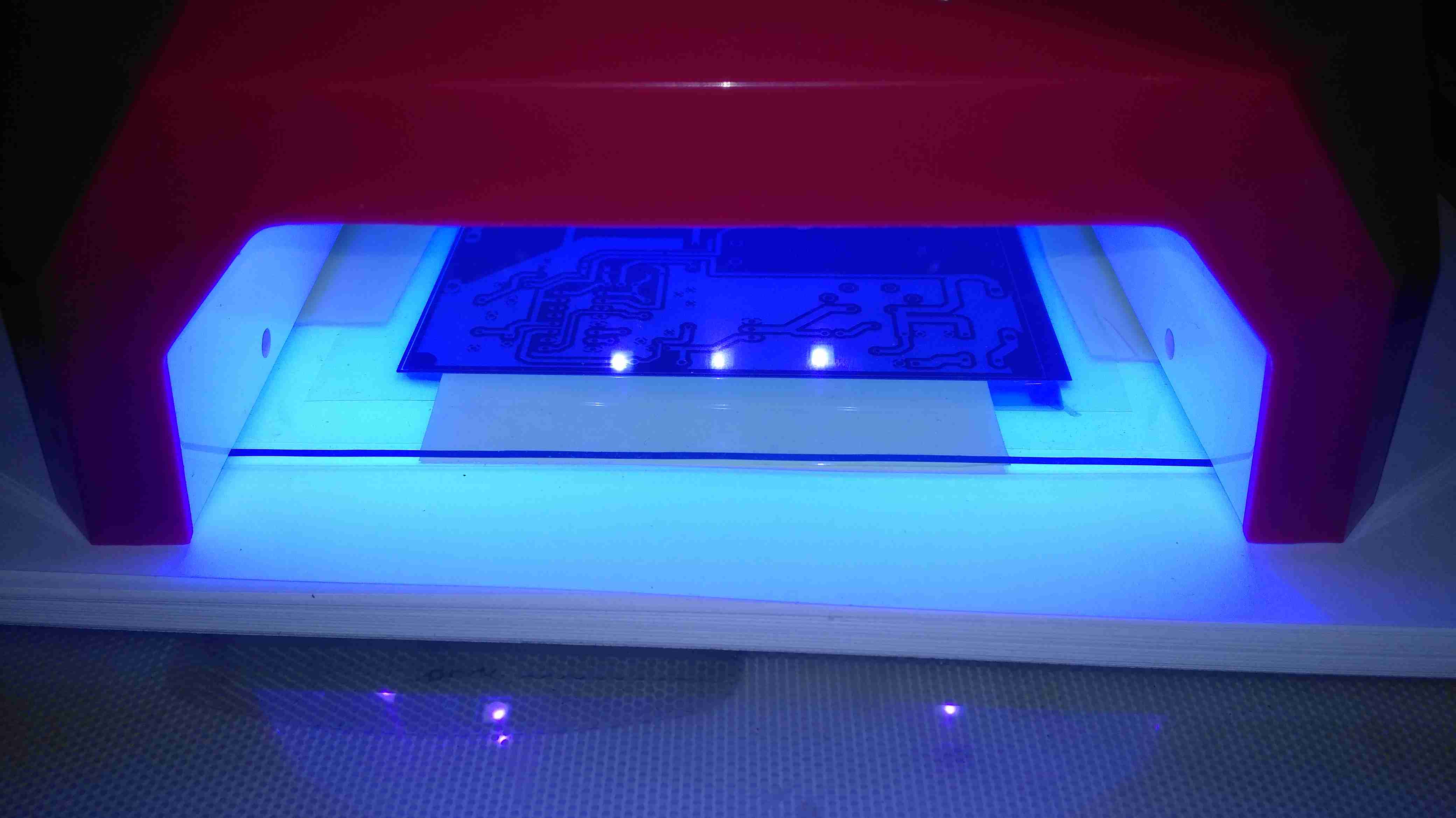
The PCB is placed on a firm surface, the exposure mask lined up on top, and the whole thing covered with a sheet of standard glass to apply even pressure. The UV exposure lamp in this case is a cheap eBay UV nail curing unit, with 15 high power LEDs. (I’ll do a teardown on this when I get some time, it’s got some very odd LEDs in it). Exposing the board for 60 seconds is all the time needed.

After Exposure
After Exposure

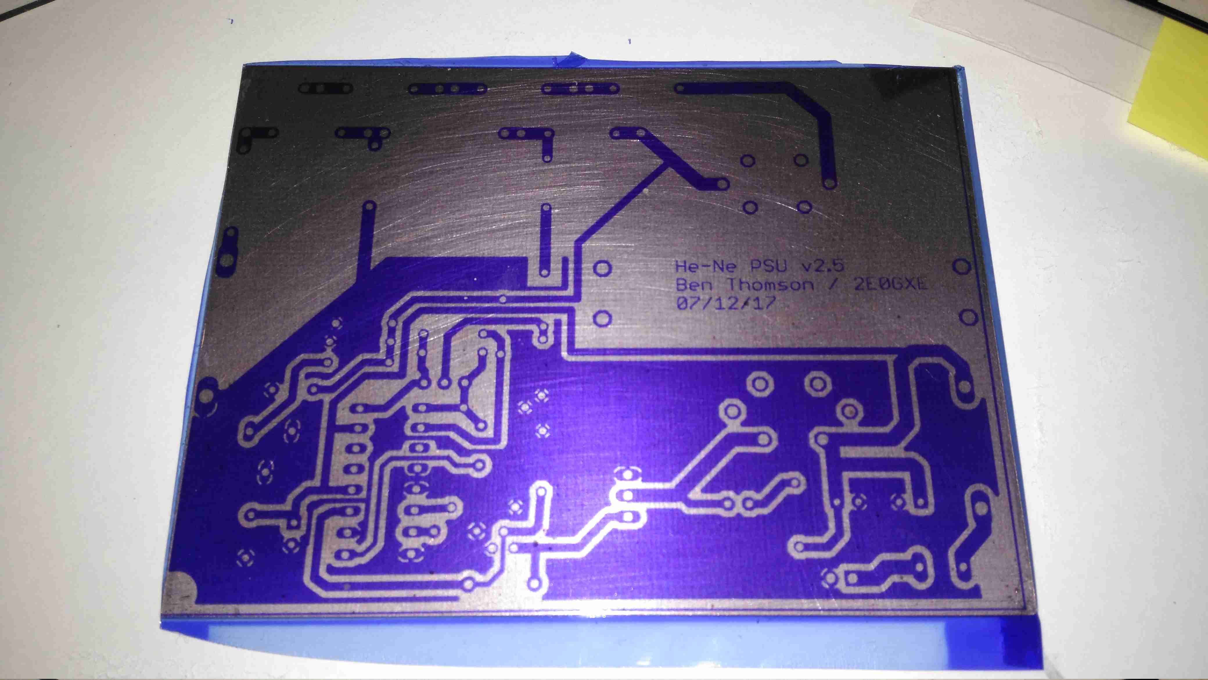
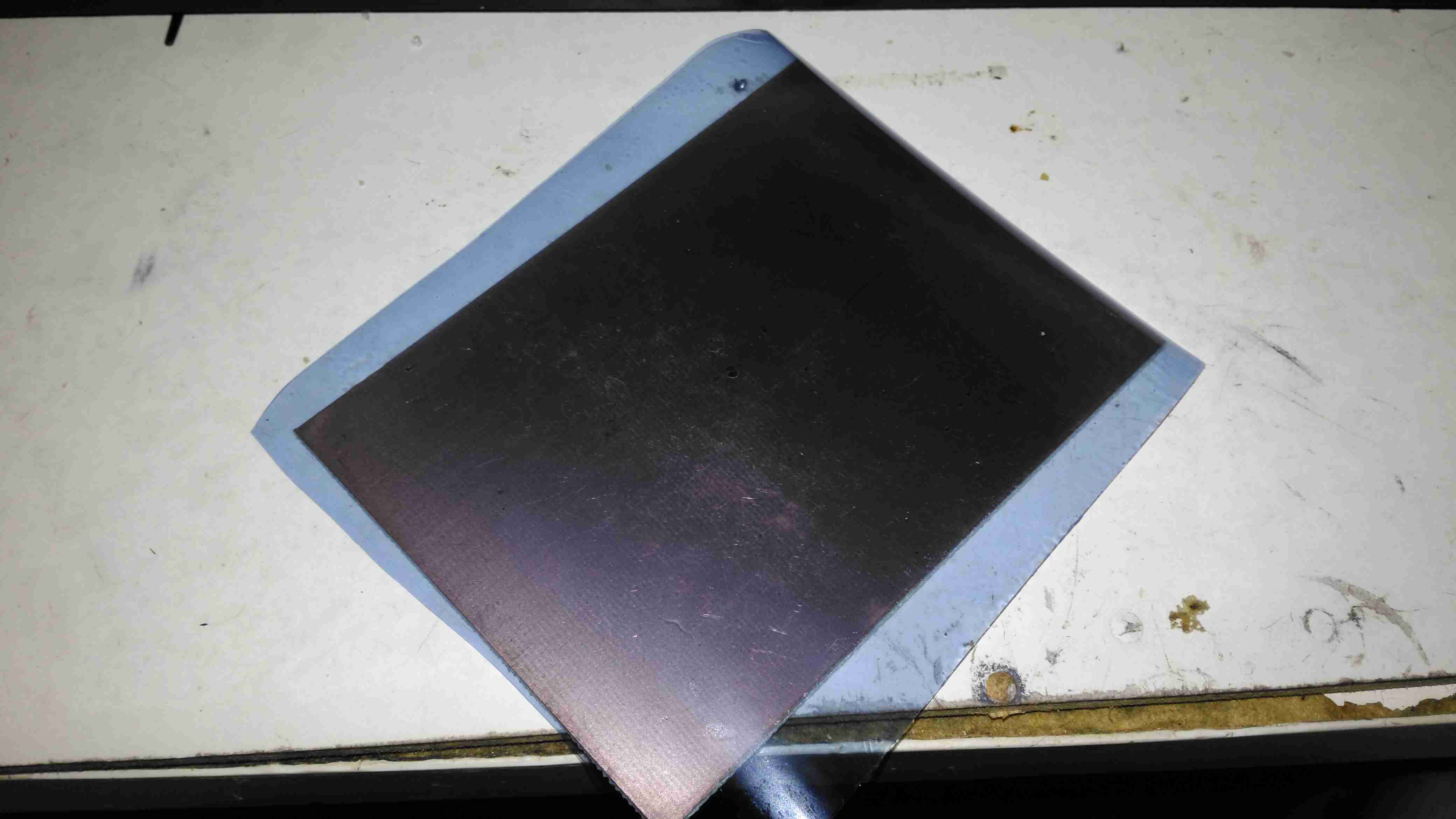
After the board is exposed, the areas that got hit with the UV light have turned purple – the resist has hardened in these areas. It’s bloody tough as well, I’ve scrubbed at it with some vigour and it doesn’t come off. Toner transfer was a bit naff in this respect, most of the time the toner came off so easily that the etchant lifted it off. After this step is done, the remaining protective film on the top can be removed.

After Developing
After Developing

The film is developed in a solution of Sodium Carbonate (washing Soda). This is mildly alkaline and it dissolves off the unexposed resist.

After Etching
After Etching

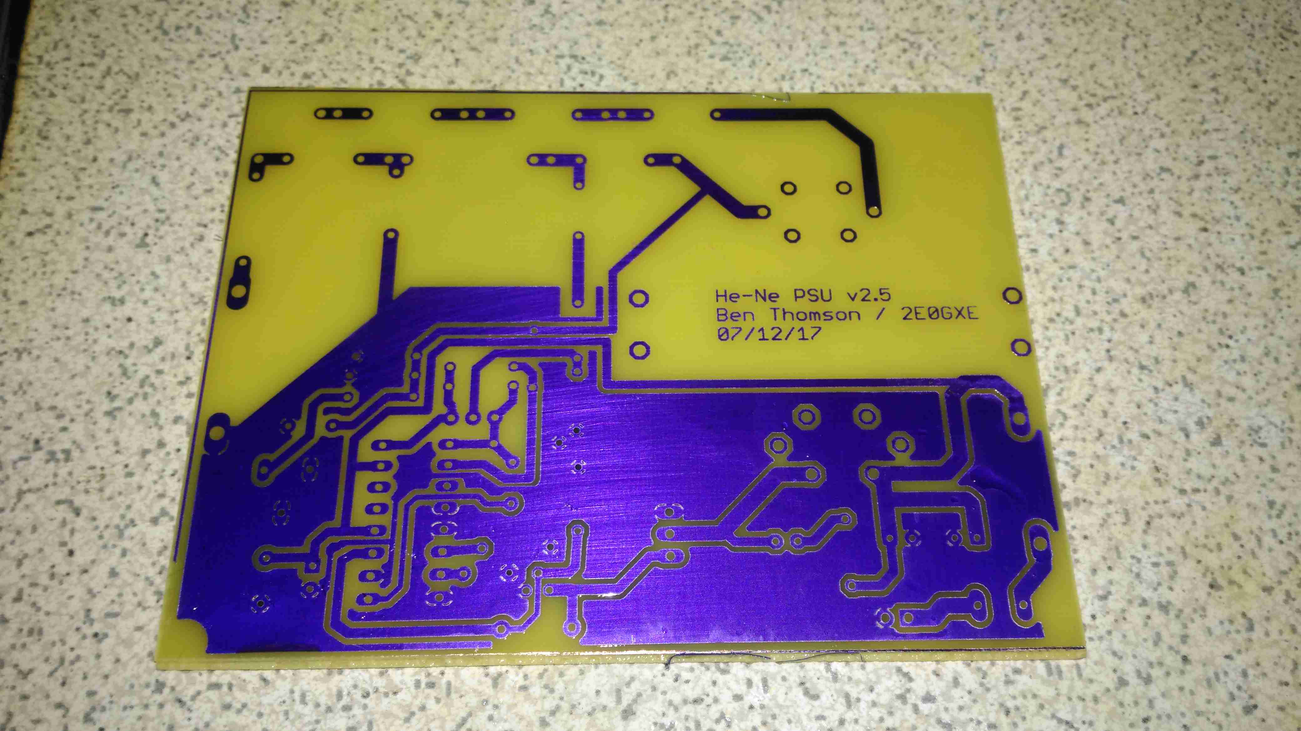
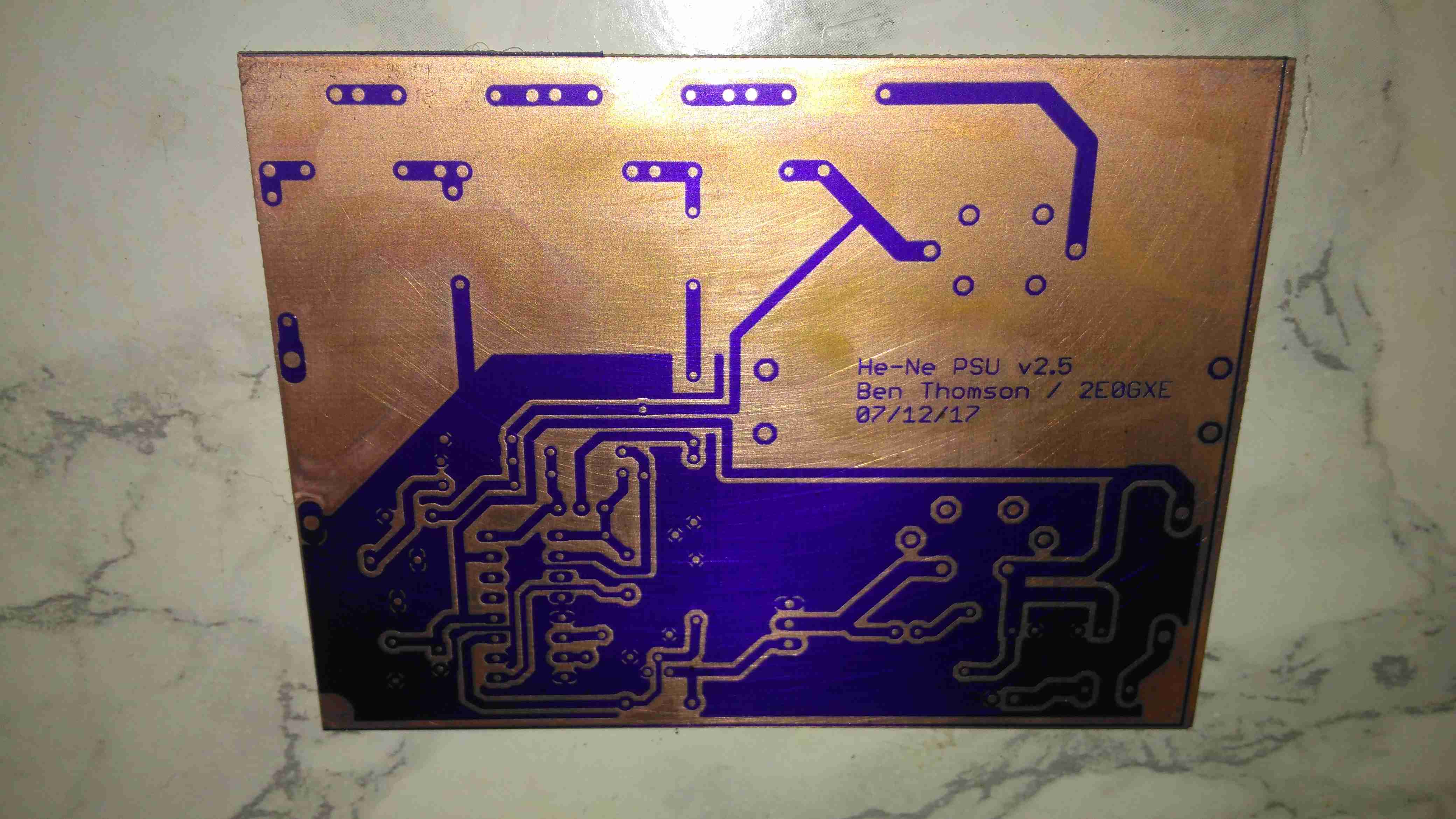
Now it’s into the etching tank for a couple of minutes, I’m still using Ferric Chloride to etch my boards, at about 60°C. Etching at room temperature is much too slow. Once this is done, the board is washed, and then dipped in the strip tank for a couple of minutes. This is a Sodium Hydroxide solution, and is very caustic, so gloves are required for this bit. Getting Ferric Chloride on skin is also a fairly bad idea, it stains everything orange, and it attacks pretty much every metal it comes into contact with, including Stainless Steel.

This method does require some more effort than the toner transfer method, but it’s much more reliable. If something goes wrong with the exposure, it’s very easy to strip the board completely & start again before etching. This saves PCB material and etchant. This is definitely more suited to small-scale production as well, since the photomask can be reused, there’s much less waste at the end. The etched lines are sharper, much better defined & even with some more chemicals involved, it’s a pretty clean process. All apart from the Ferric Chloride can be disposed of down the sink after use, since the developer & stripper are just alkaline solutions.


Posted on 2 Comments

EpEver MT50 Control Panel Teardown

MT50 Control Panel
MT50 Control Panel

Here’s the MT50 controller from EpEver, that interfaces with it’s Tracer MPPT solar charge controllers, and gives access to more programming options on the charge controllers, without the need for a laptop. The display is a large dot-matrix unit, with built in backlight. Above is the display on the default page, showing power information for the entire system.

PCB Rear
PCB Rear

The rear plastic cover is held in place by 4 machine screws, which thread into brass inserts in the plastic frame – nice high quality touch on the design here, no cheap self tapping plastic screws. Both power & data arrive via an Ethernet cable, but the communication here is RS-485, and not compatible with Ethernet! The PCB is pretty sparse, with comms & power on the left, LCD connection in the centre, and the microcontroller on the right.

RS-485 Transceiver
RS-485 Transceiver

On the left of the board is the RS0485 transceiver, and a small voltage regulator. There’s also a spot for a DC barrel jack, which isn’t included in this model for local power supply.

STM32 Microcontroller

The other side of the board holds the main microcontroller which communicates with the charge controller. This is a STM32F051K8 from ST Microelectronics. With a 48MHz ARM Cortex M0 core, and up to 64K of flash, this is a pretty powerful MCU that has very little to do in this application.

PCB Front
PCB Front

The front of the PCB has the ENIG contacts of the front panel buttons, and the LCD backlight assembly. There’s nothing else under the plastic backlight spreader either.

LCD Rear
LCD Rear

The front case holds the LCD module in place with glue, and the rubber buttons are placed underneath, which is heat staked in place.

LCD Model
LCD Model

The LCD is a YC1420840CS6 from eCen in China. Couldn’t find much out about this specific LCD.

Posted on Leave a comment

“SolarStorm” eBay 4x 18650 Battery Pack

Pack Top
Pack Top

Since the 4×18650 battery pack supplied with my Cree head torch is pretty shit, even by China’s standards, I figured something I could put my own cells into would be a better option. An eBay search turned up these battery boxes, not only with a direct battery output for my torch, but also a USB port for charging other devices when I’m low on charge.

LED Capacity Indicator

The output to the lamp connector is directly connected to the battery, through the usual Lithium Ion protection, but the USB output is controlled from a single power button. Battery charge condition is displayed on 3 LEDs. Not sure why they used blue silicone for the seal & then used green LEDs… But it does work, even if a little dim.

Label
Label

Essential information. Does claim to be protected, and from the already existing electronics for the USB this would be expected in all but the cheapest crap.
An IP rating of IPX4 is claimed, yet just above that rating is a notice not to be used in water. Eh?
This is sealed with an O-Ring around the edge of the top cap & silicone seals around the cable & retaining screw. I did test by immersion in about 6″ of water, and it survived this test perfectly fine, no water ingress at all.

Interconnect Straps
Interconnect Straps

The casing holds a PCB at the bottom end with the cell straps.

Screw Post
Screw Post

Someone wasn’t that careful at getting the brass screw insert properly centred in the injection mould when they did this one. It’s mushed off centre, but i’s solidly embedded & doesn’t present any problems to usability.

Cell Springs
Cell Springs

The top cover holds the cell springs & the electronics.

Button & Cable Seal
Button & Cable Seal

Removing the pair of screws allows the top cap to open up. The cable, button & LEDs are robustly sealed off with this silicone moulding.

Top Removed
Top Removed

Here’s the PCB, not much on the top, other than the power button & battery indicator LEDs.

Electronics
Electronics

Desoldering the cell springs allows the PCB to pop out of the plastic moulding. There’s more than I expected here!

Bottom left is a DC-DC converter, generating the +5v rail for the USB port, this is driven with an XL1583 3A buck converter IC.

Bottom right is the protection IC & MOSFETs for the Lithium Ion cells. I wasn’t able to find a datasheet for the tiny VA7022 IC, but I did manage to make certain it was a 7.4v Li-Ion protection IC.

Top right is a completely unmarked IC, and a 3.3v SOT-23 voltage regulator. I’m assuming that the unmarked IC is a microcontroller of some sort, as it’s handling more than just the battery level LEDs.

A pretty decent 4-core cable finishes the job off. For once there’s actually some copper in this cable, not the usual Chineseuim thin-as-hair crap.

Posted on Leave a comment

Another Chinese Charger

I almost forgot about this bit of kit, that came with one of my LED torches as a Lithium Ion charger. As I never plug in anything that comes from China via eBay, here’s the teardown & analysis.

Another Lethal Charger?

Here’s the unit itself. It’s very light, and is clearly intended for American NEMA power points.

Specs
Specs

Claimed specifications are 100-240v AC input, making it universal, and 4.2v DC out ±0.5v at 500mA.
Considering the size of the output wire, if this can actually output rated voltage at rated current I’ll be surprised.

Opened
Opened

Here’s the adaptor opened up. There’s no mains wiring to speak of, the mains pins simply push into tags on the PCB.

PCB Top
PCB Top

Top of the SMPS PCB. As usual with Chinese gear, it’s very simple, very cheap and likely very dangerous. There’s no real fusing on the mains input, only half-wave rectification & no EMI filtering.

PCB Bottom
PCB Bottom

Here’s the bottom of the PCB. At least there’s a fairly sized gap between the mains & the output for isolation. The wiggly bit of track next to one of the mains input tags is supposed to be a fuse – I somehow doubt that it has the required breaking characteristics to actually pass any safety standards. Obviously a proper fuse or fusible resistor was far too expensive for these.

The output wiring on the left is thinner than hair, I’d say at least 28AWG, and probably can’t carry 500mA without suffering extreme volt drop.

Posted on Leave a comment

Potentially Lethal Clone Apple Charger

Charger
Charger

I received this USB supply with a laser module from China that I purchased on eBay. I have heard of these nasty copies of Apple chargers going around, but I’d never received one this bad with a piece of Chinese electronics.

Label
Label

Model No. A1265, so definitely an Apple clone. Apparently capable of +5v DC 1A output. Notice the American NEMA pins. This wouldn’t have been any use to me in the first instance since I am resident in the UK & our mains plugs are significantly different, not to mention significantly safer.

Manufacturer is marked as Flextronics.

Top Of Boards
Top Of Boards

Here is the charger disassembled. Inside the case these two boards are folded together, creating an alarmingly small isolation gap between the mains side of the supply & the 5v output. Both the low voltage output & the feedback loop for the supply runs over the 4-core ribbon cable.
The mains wiring from the board is as thin as hair, insulation included, so there is a big possibility of shorts all over the place from this part of the circuit alone.

Bottom Of Boards
Bottom Of Boards

Bottom of the PCB assemblies. Good luck finding any creepage distance here. There simply isn’t any at all. traces on the +350v DC rail on the mains side of the transformer are no more than 1mm away from the supposedly isolated low voltage side.

Plugging one of these devices into anything is just asking for electrocution.