Posted on 10 Comments

Sony HVC-3000P Trinicon Camera Teardown

Camera Left
Camera Left

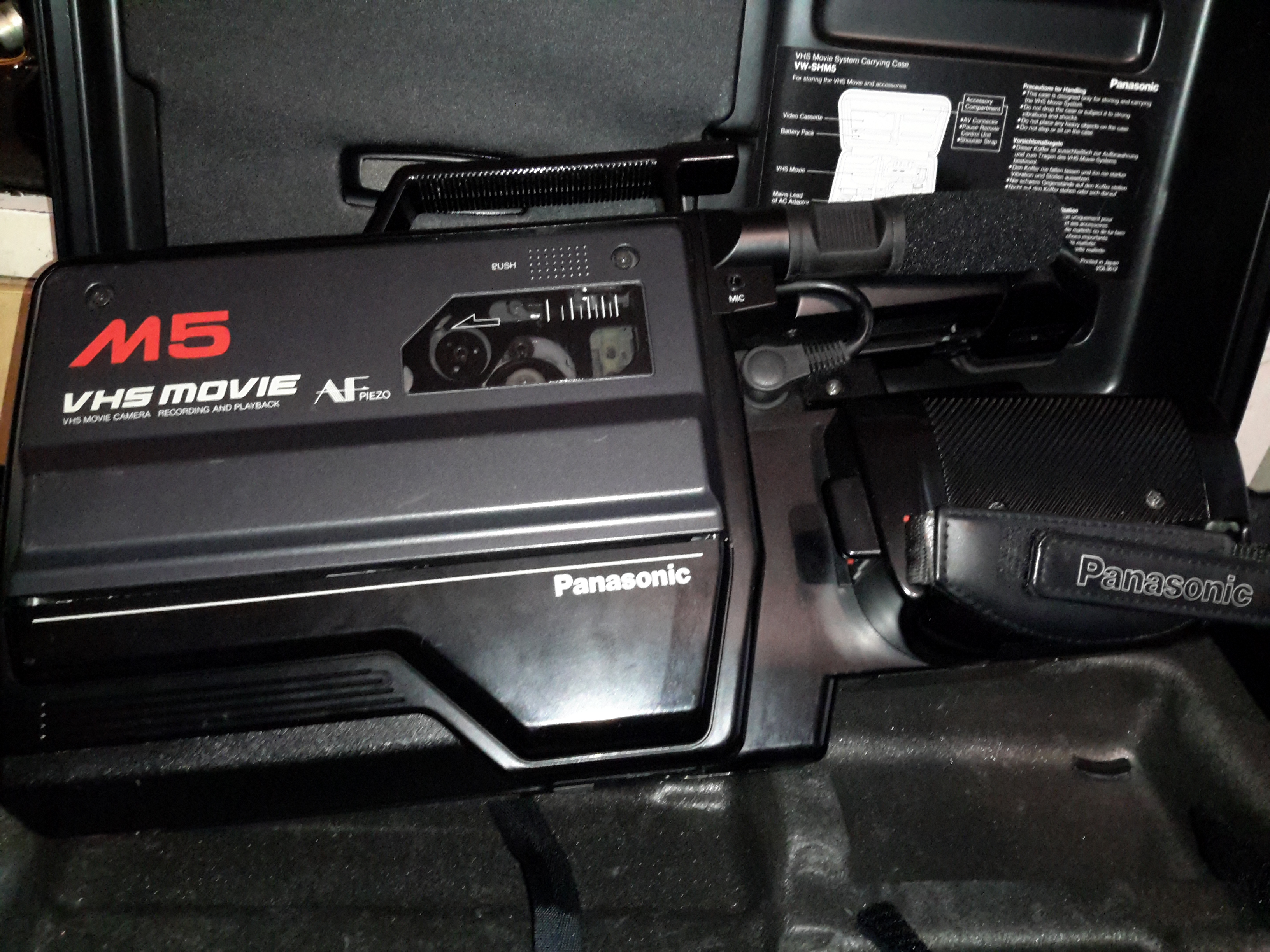
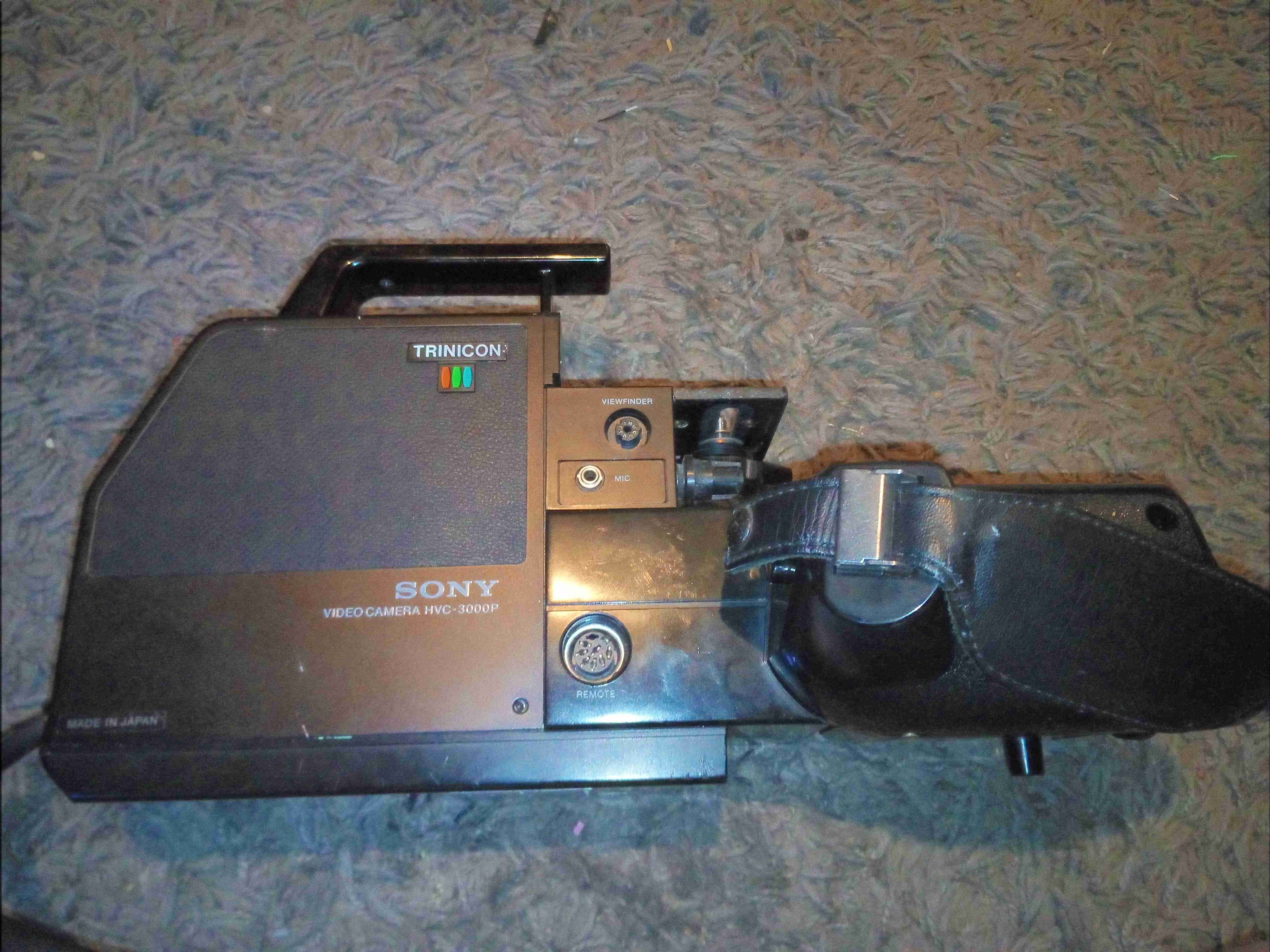
Following on from the viewfinder teardown, here’s the rest of the camera. This unit dates back to 1980, and is made almost exclusively of cast aluminium. Very little plastic has been used here & only for the bits that the user comes into contact with. This camera is based around the Sony Trinicon camera tube system, technology dating back before CCDs. There aren’t many controls on this side of the camera, only the record button, which is hidden behind the camera handgrip.

Camera Right
Camera Right

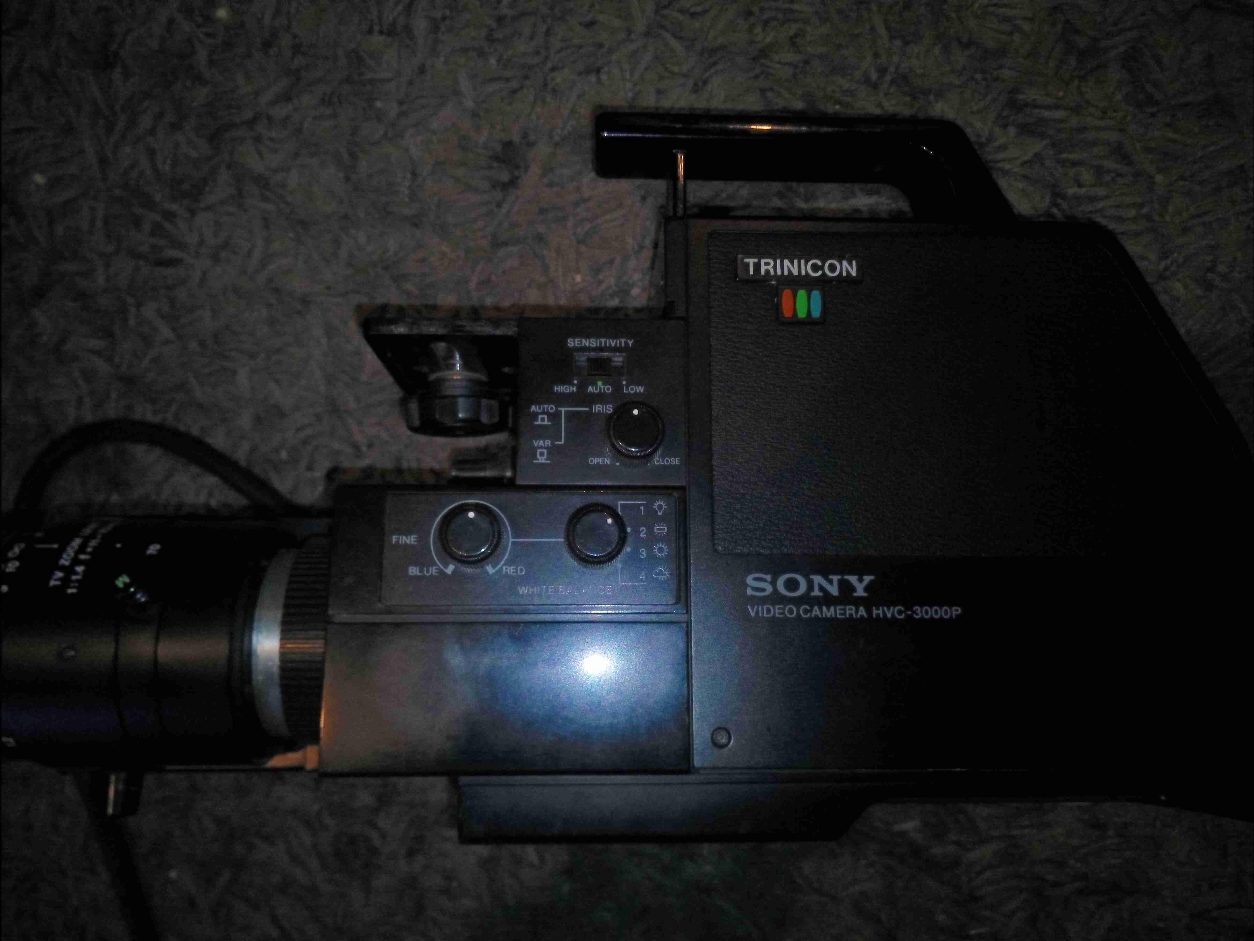
The other side of the camera has most of the controls for the picture.

Image Controls
Image Controls

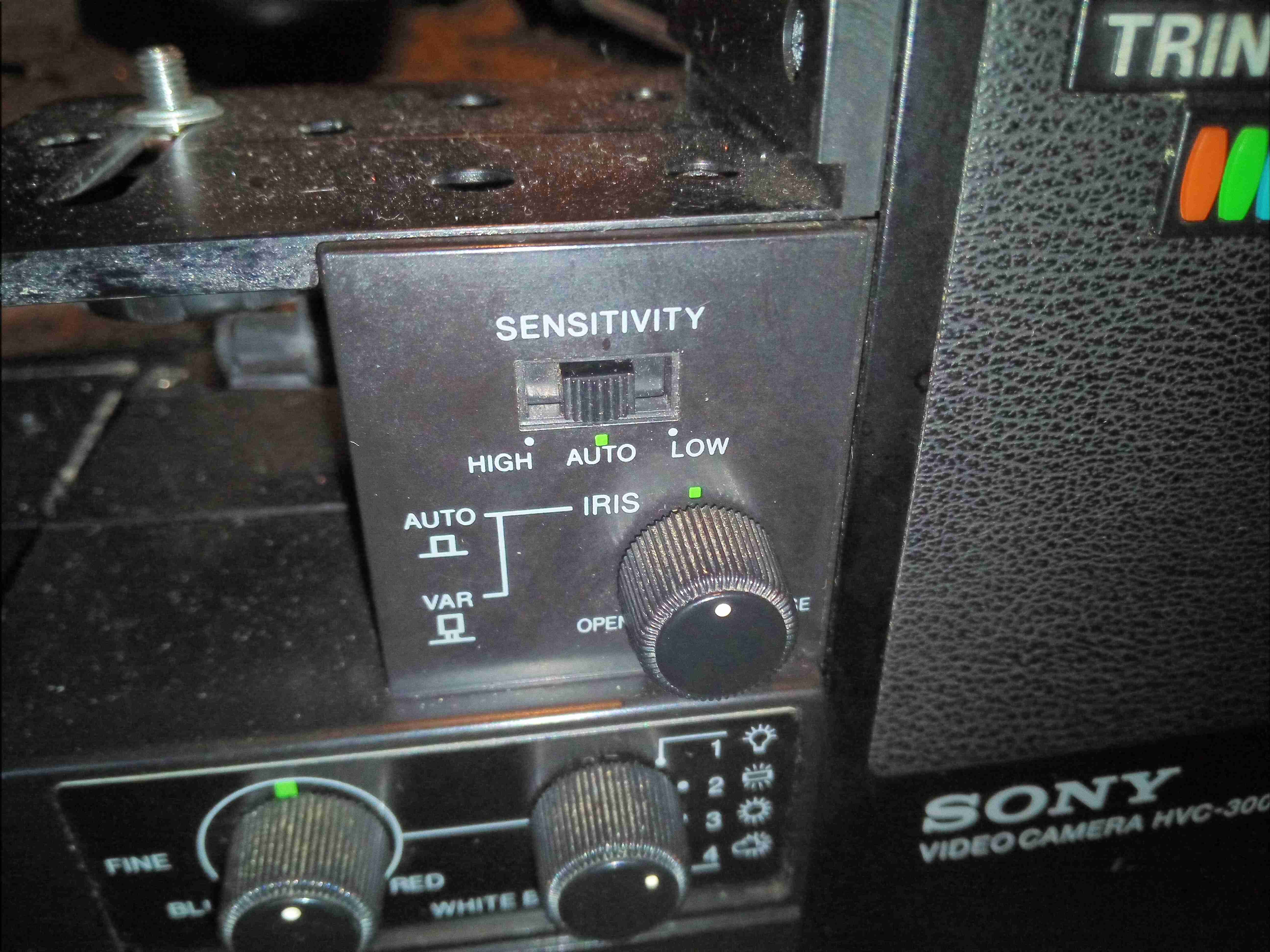
The image controls inclue auto / manual iris, white balance & colour balance.

Rear Panel
Rear Panel

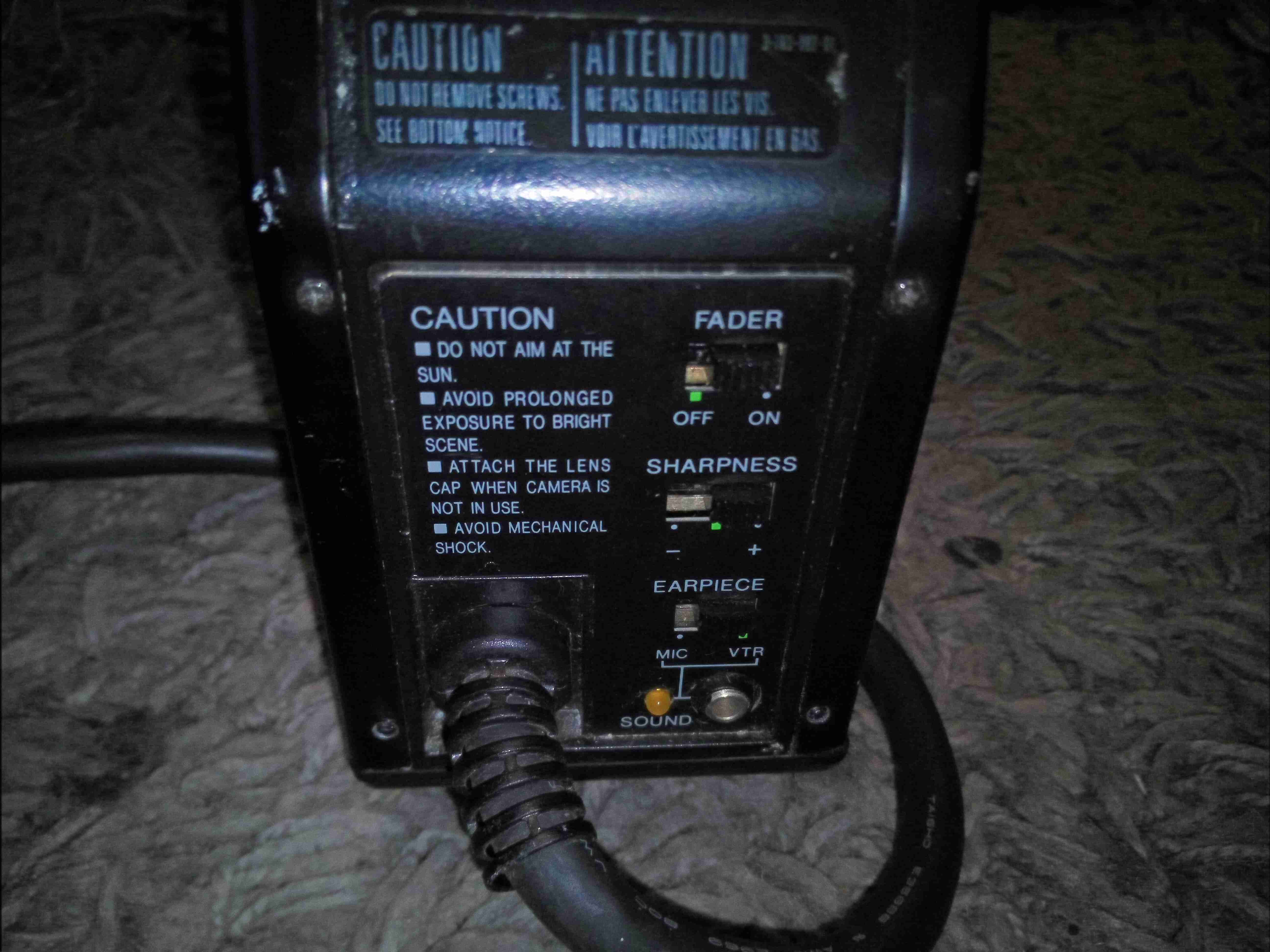
Sharpness & fader controls are on the back of the camera, along with the umbilical cable which would have connected to a Betamax recorder.

Main Lens
Main Lens

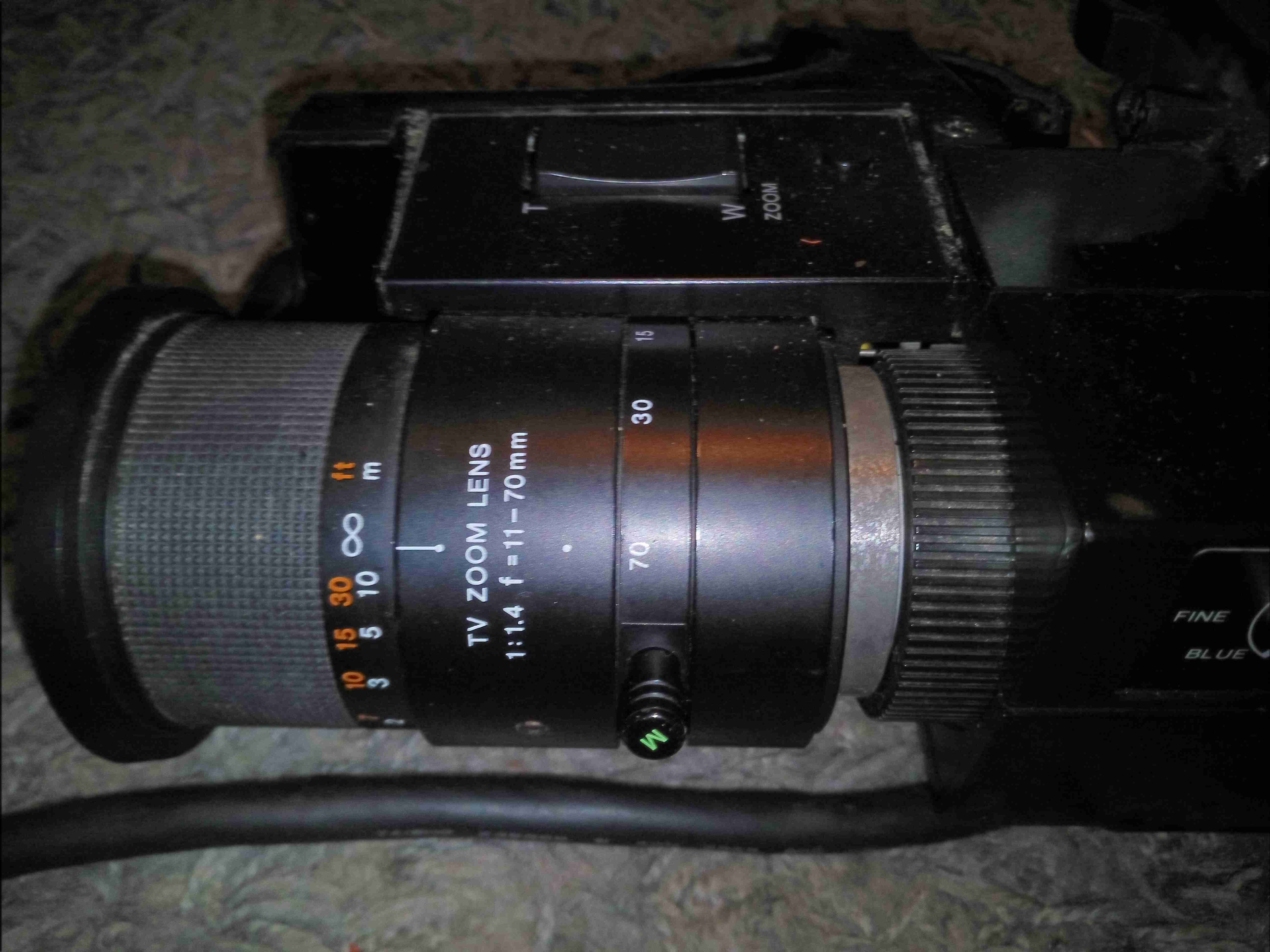
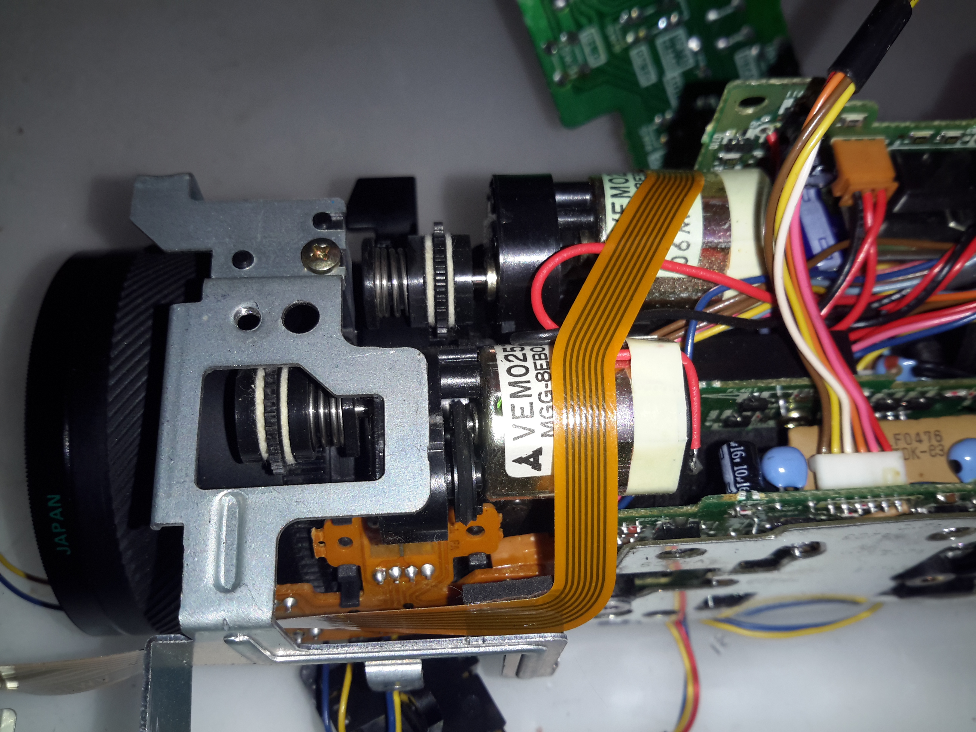
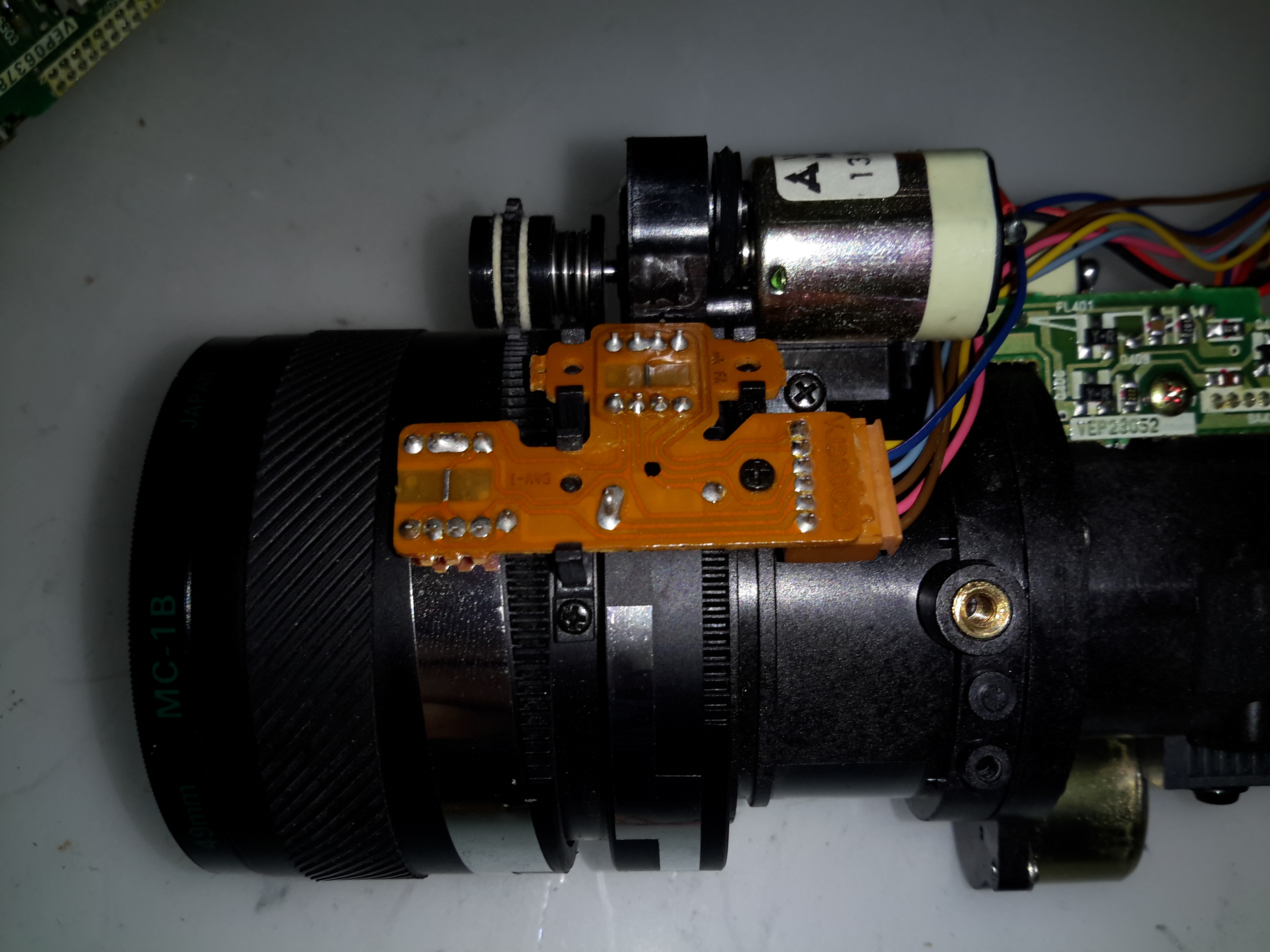
The lens on this camera is massive, at least a kilo of optical glass. Focus control is manual, with both auto & manual zoom control.

Lens Zoom Control
Lens Zoom Control

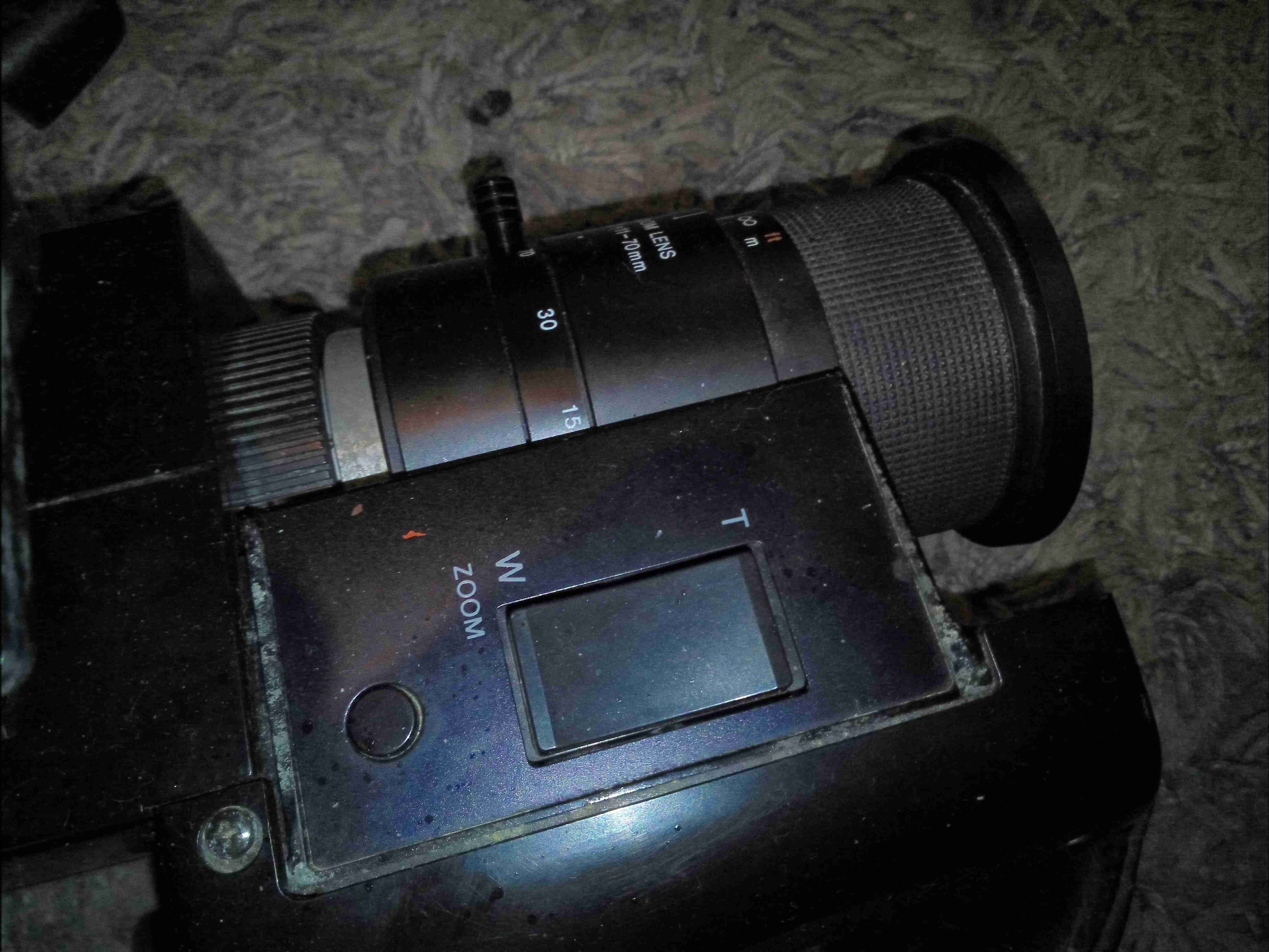
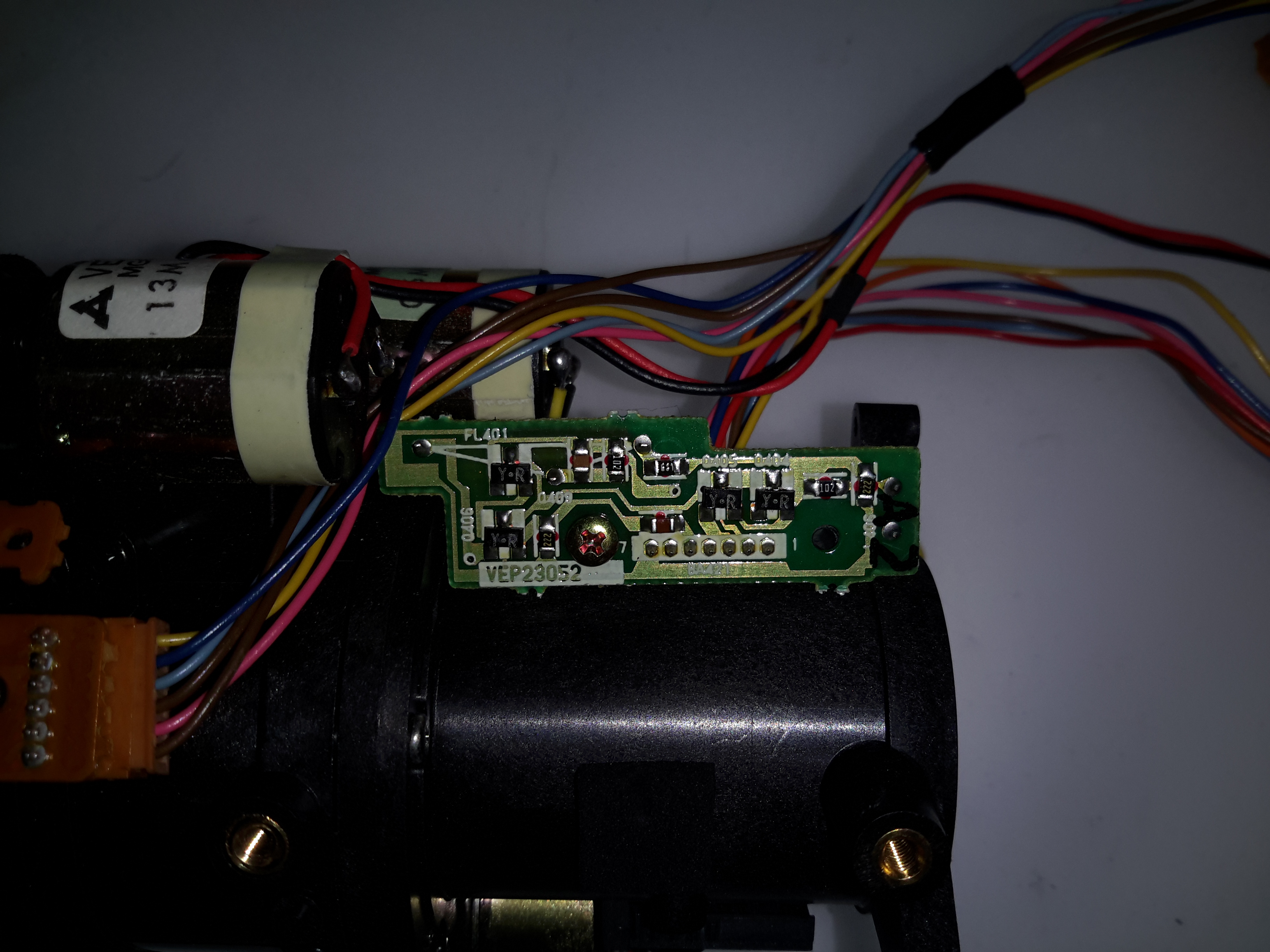
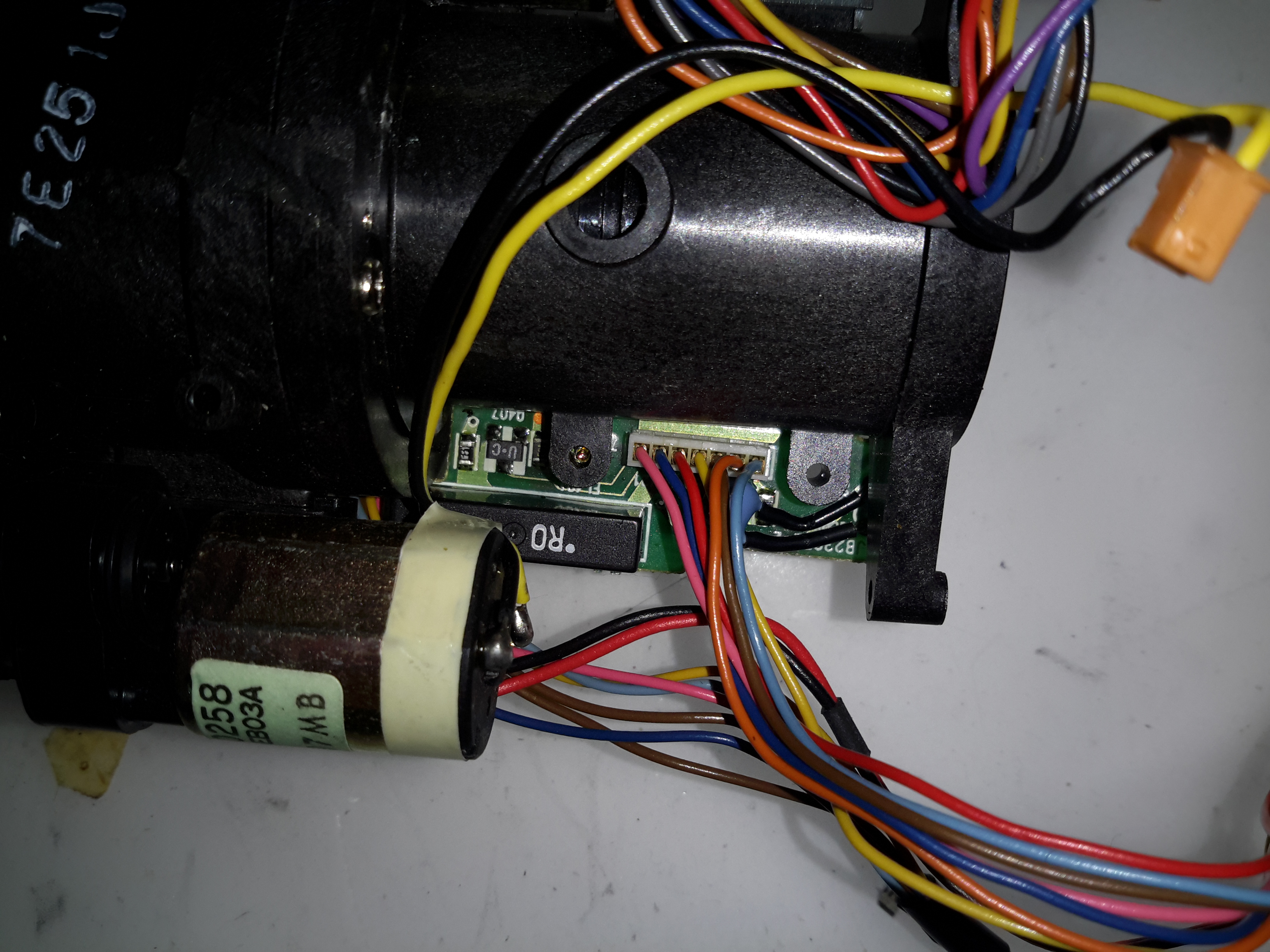
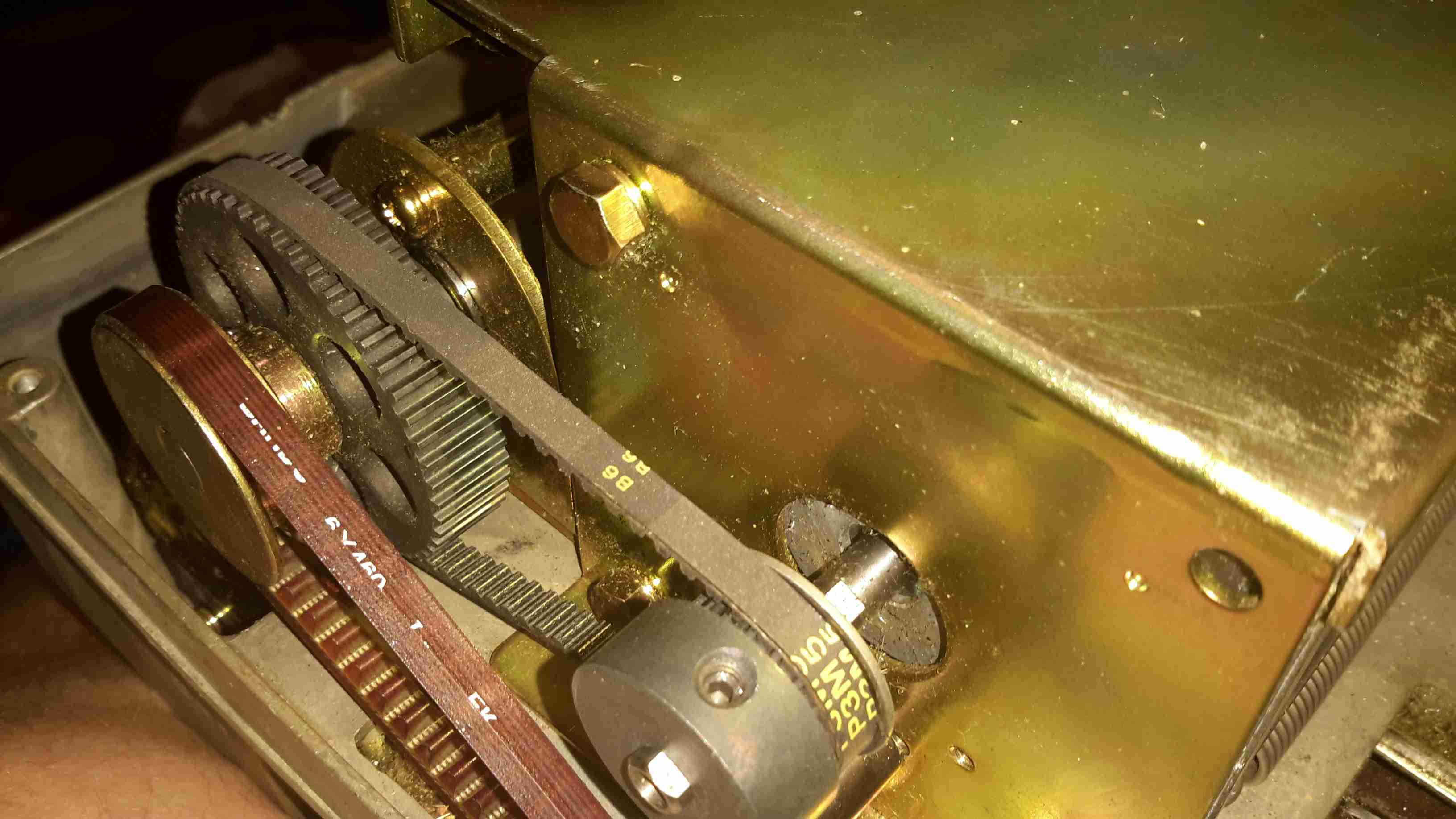
The Zoom controls are on top of the grip, with a button to the rear of the control which I have no idea about. The internal belts are a bit rotted with age so the zoom function doesn’t work great.

Trinicon Control Board

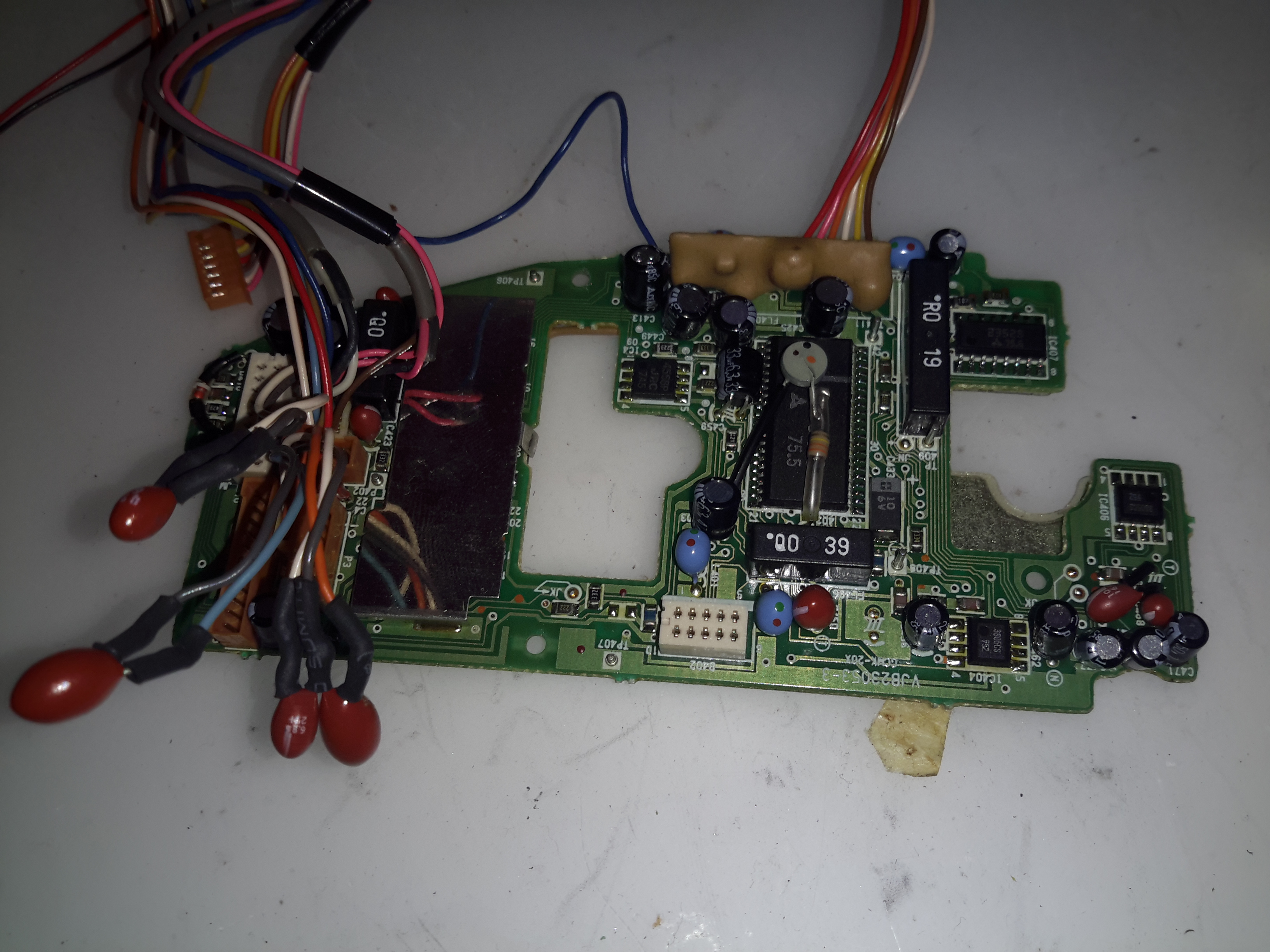
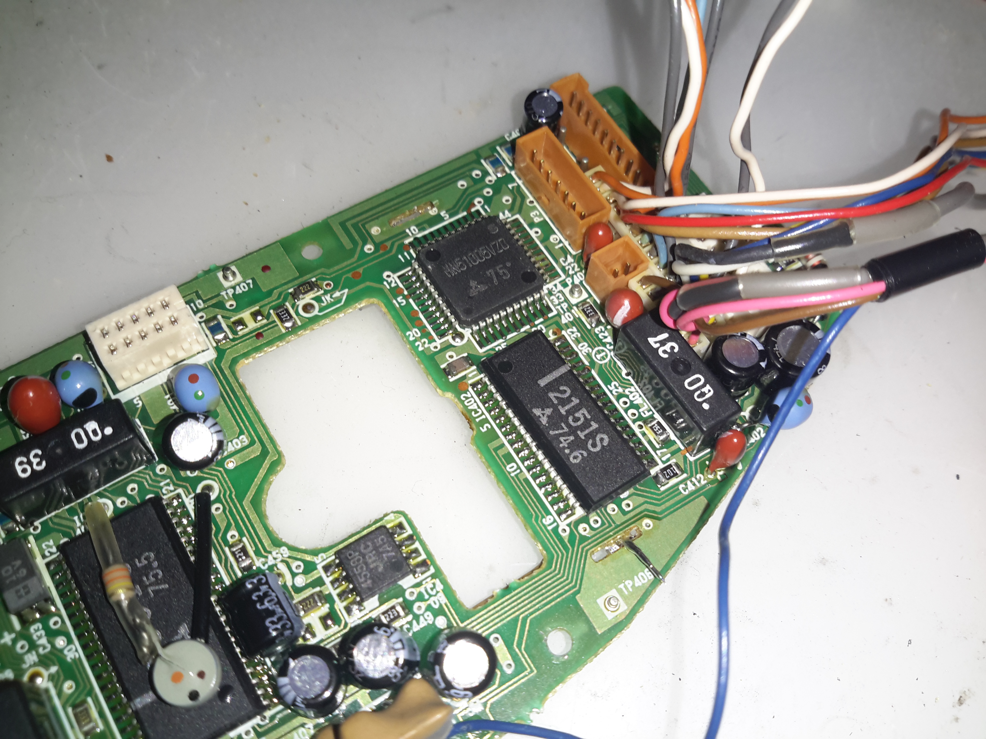
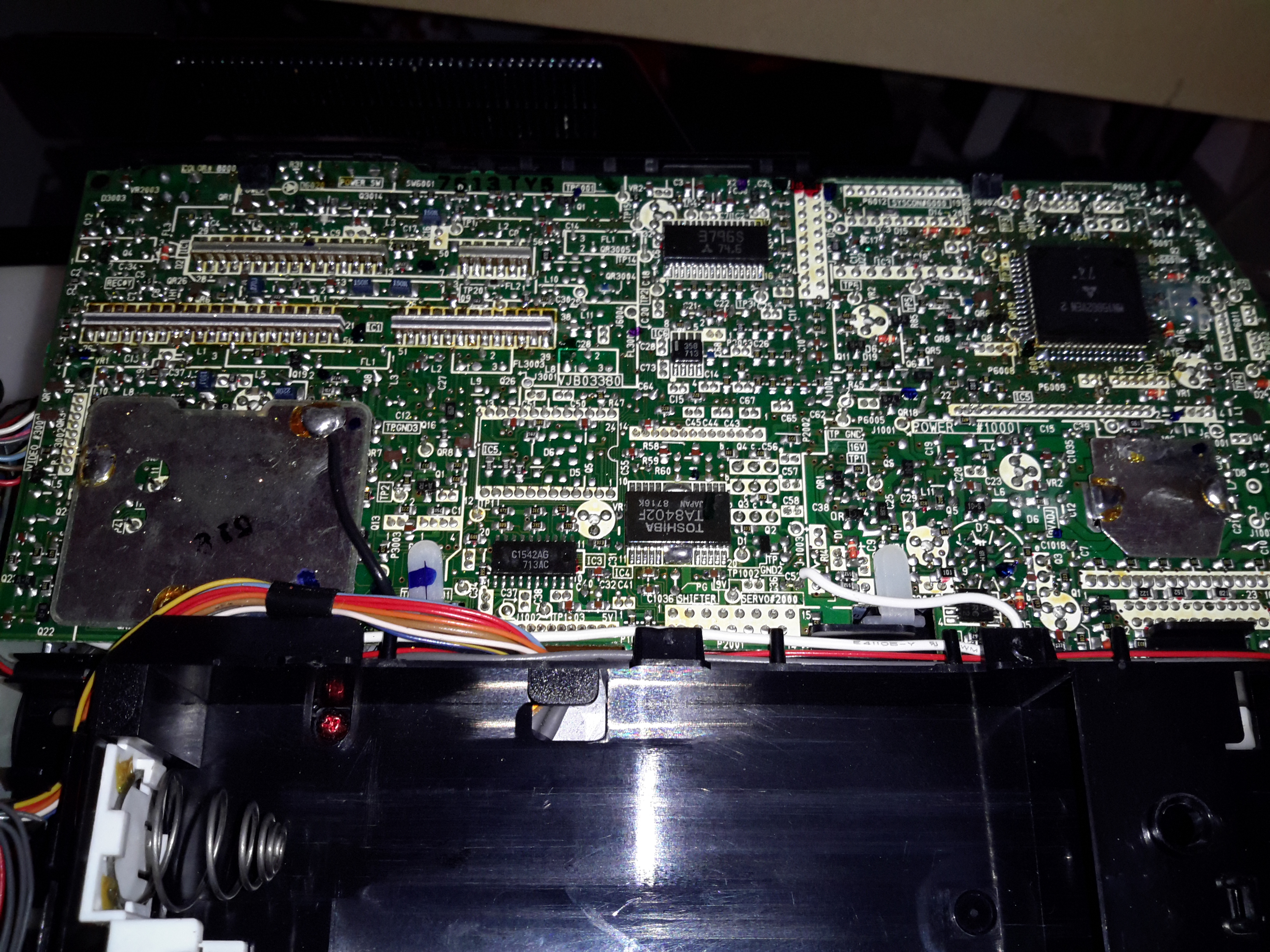
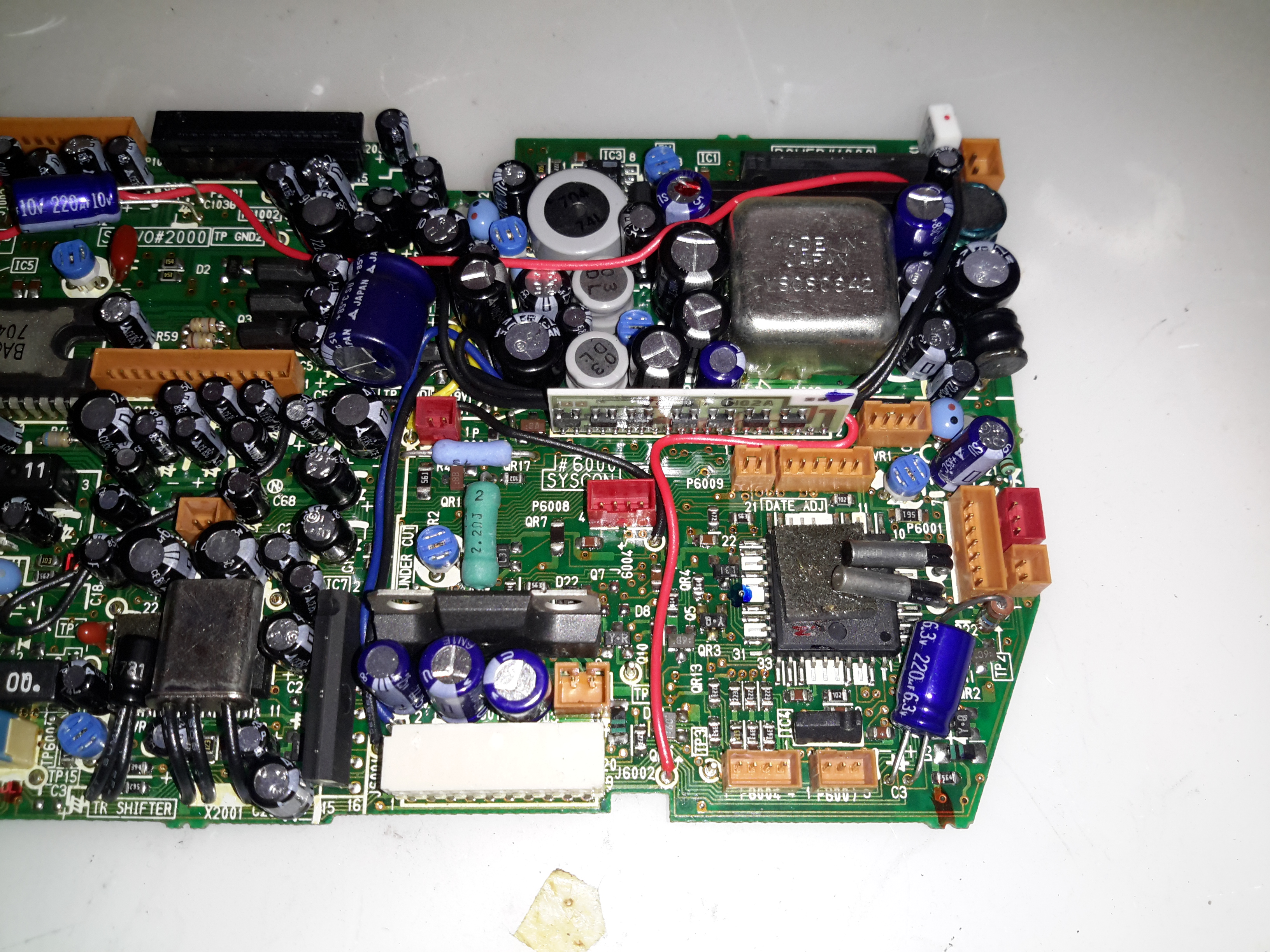
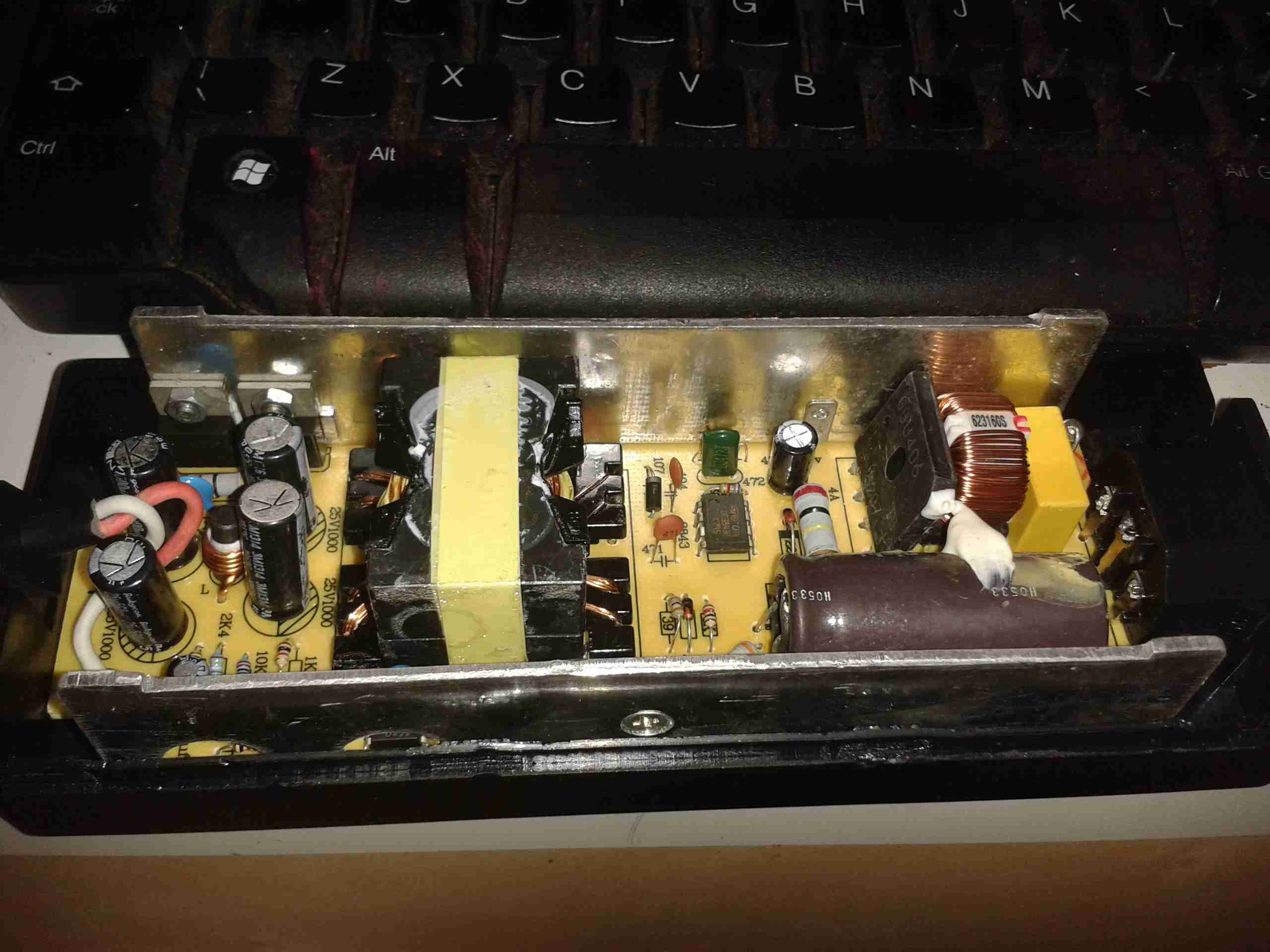
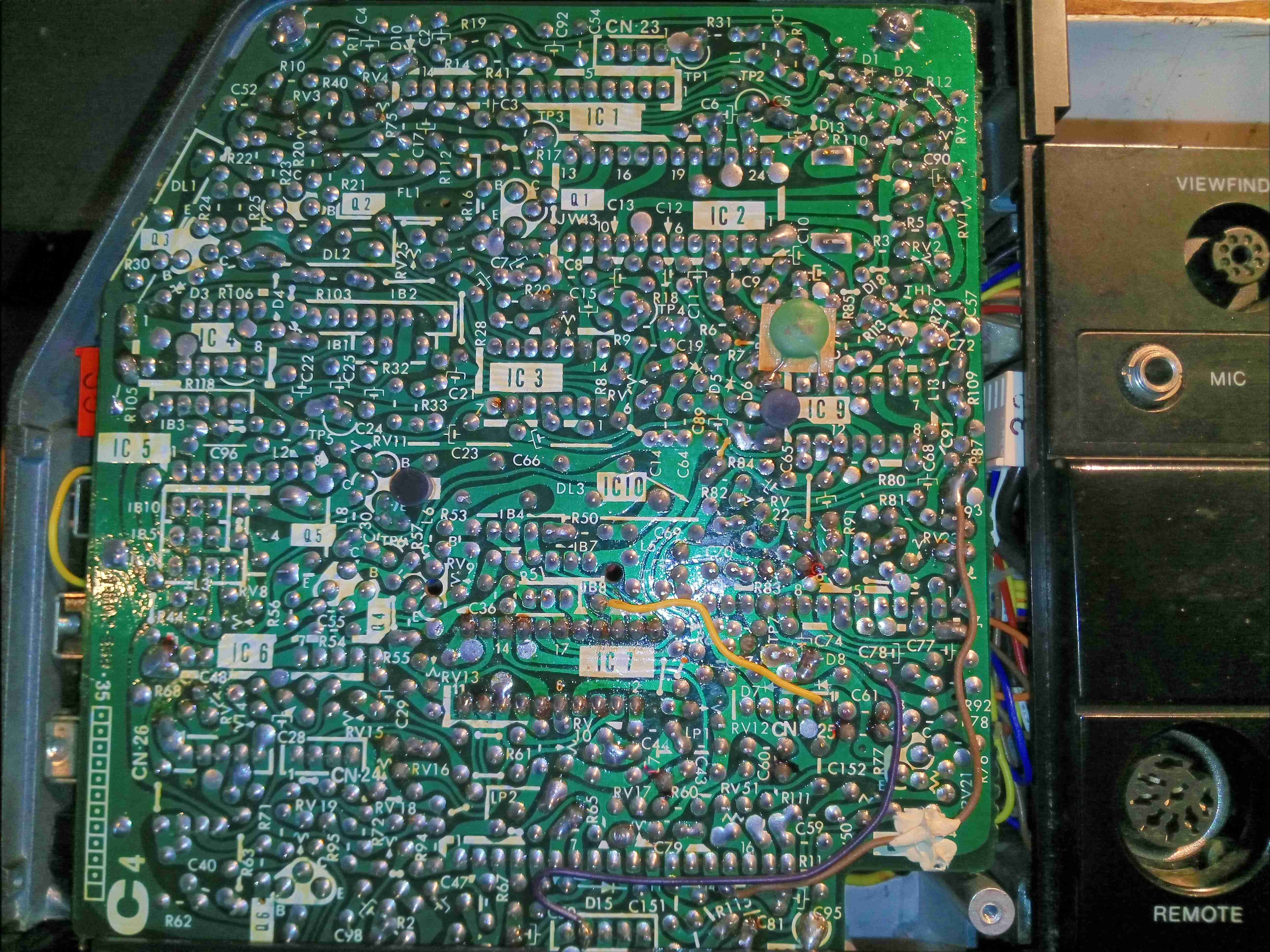
After removing the side covers, the two large PCBs become visible. These units are absolutely packed with electronics. On this side is the Trinicon tube control board, generating all the high voltages for electron beam acceleration, focus & electrostatic deflection of the beam. There’s around 500 volts knocking around on this board, with some rather specialised hybrid modules doing all the high voltage magic.

Video Process Board
Video Process Board

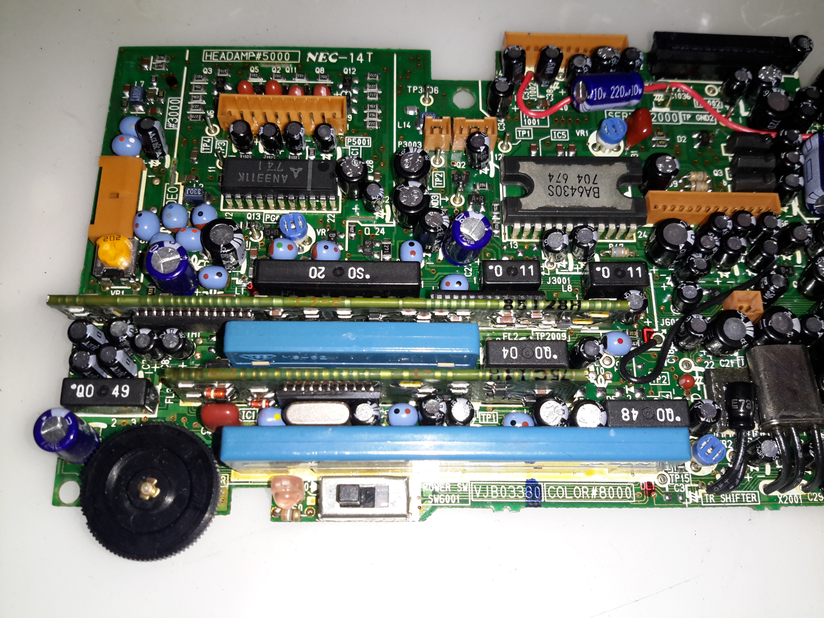
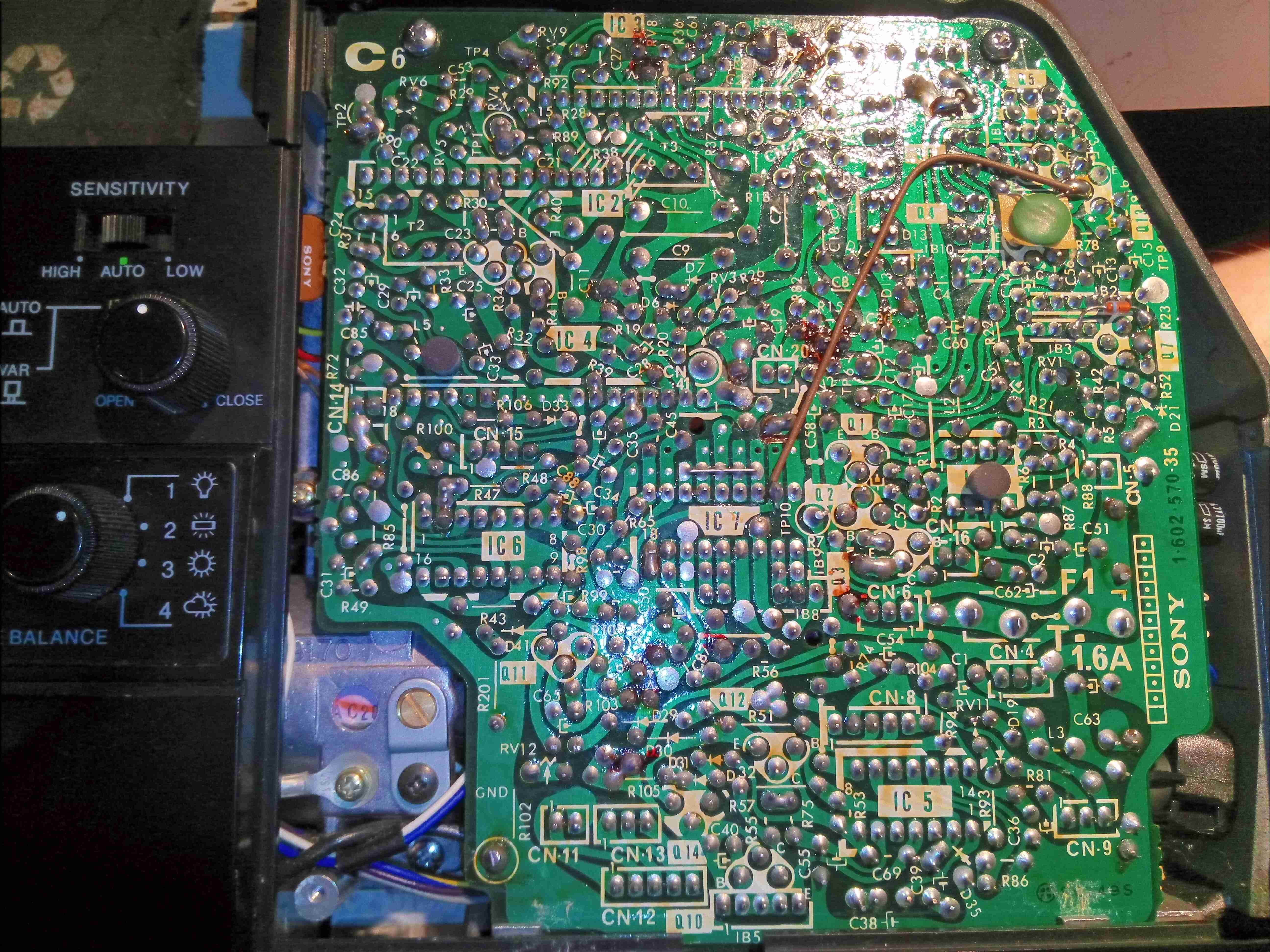
The other side of the camera has the video process board, which performs all the colour separation of the video signal from the tube, processes the resulting signals into a composite video signal, and finally sends it down the umbilical.

Bare Controls
Bare Controls

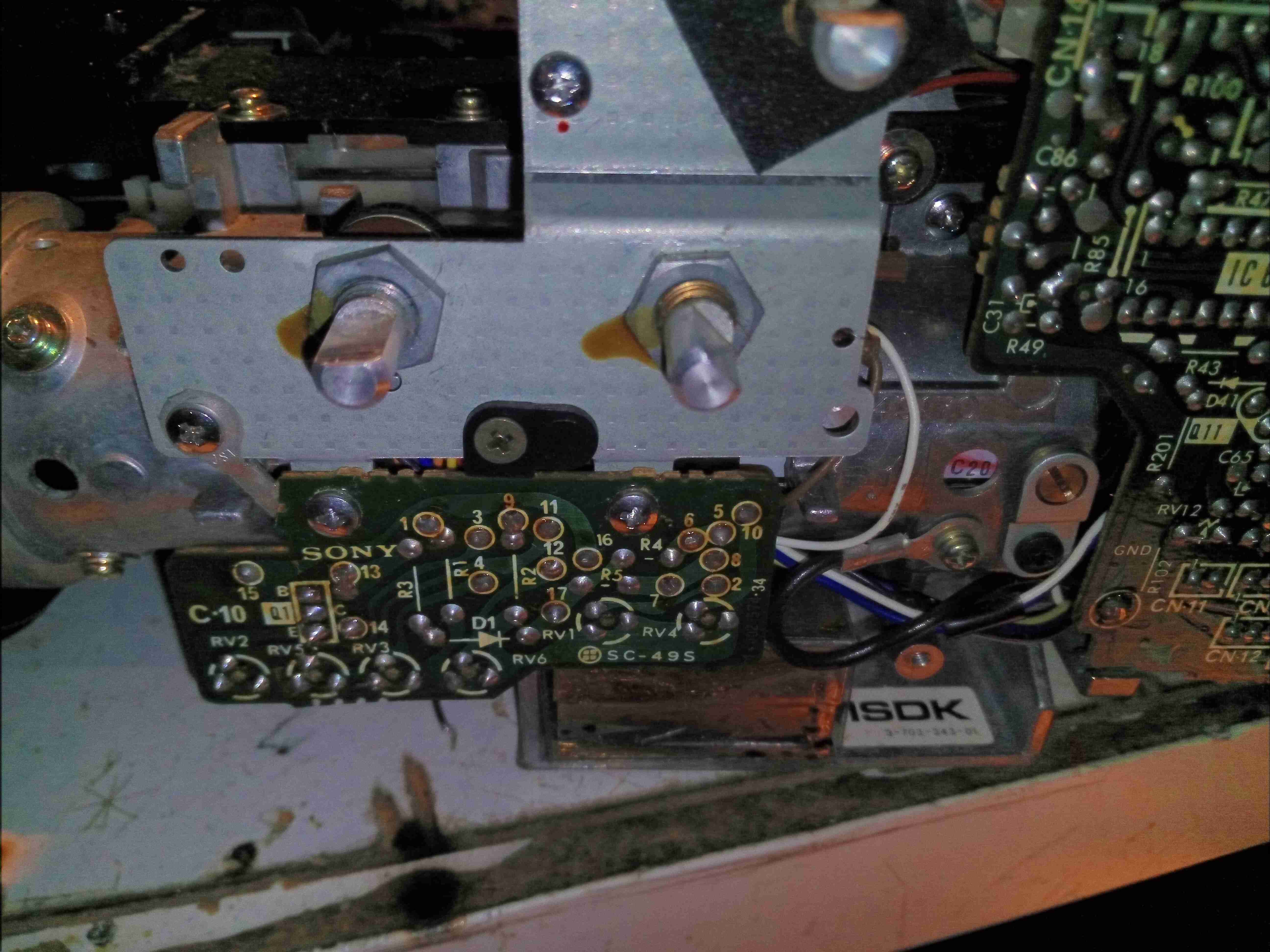
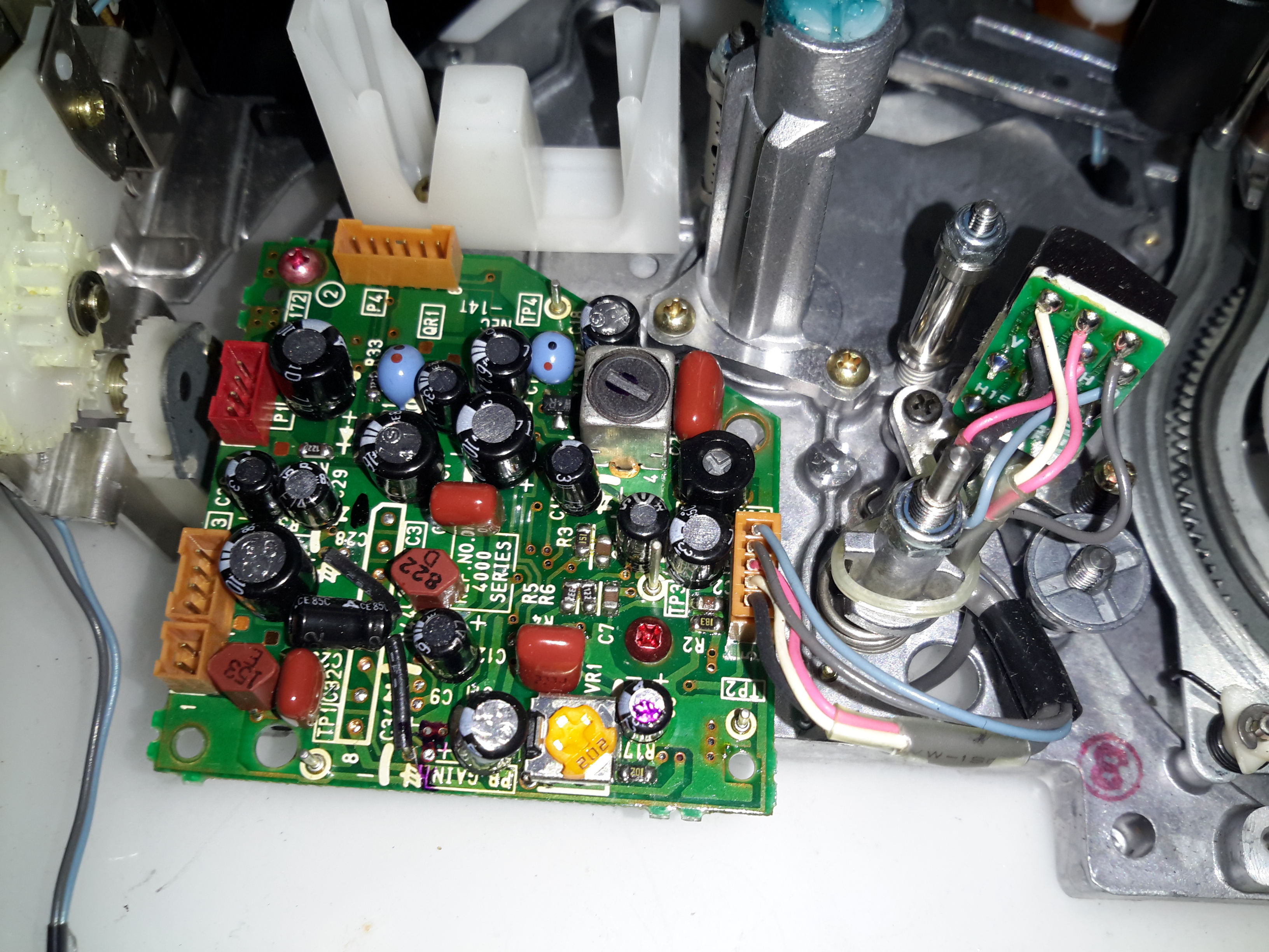
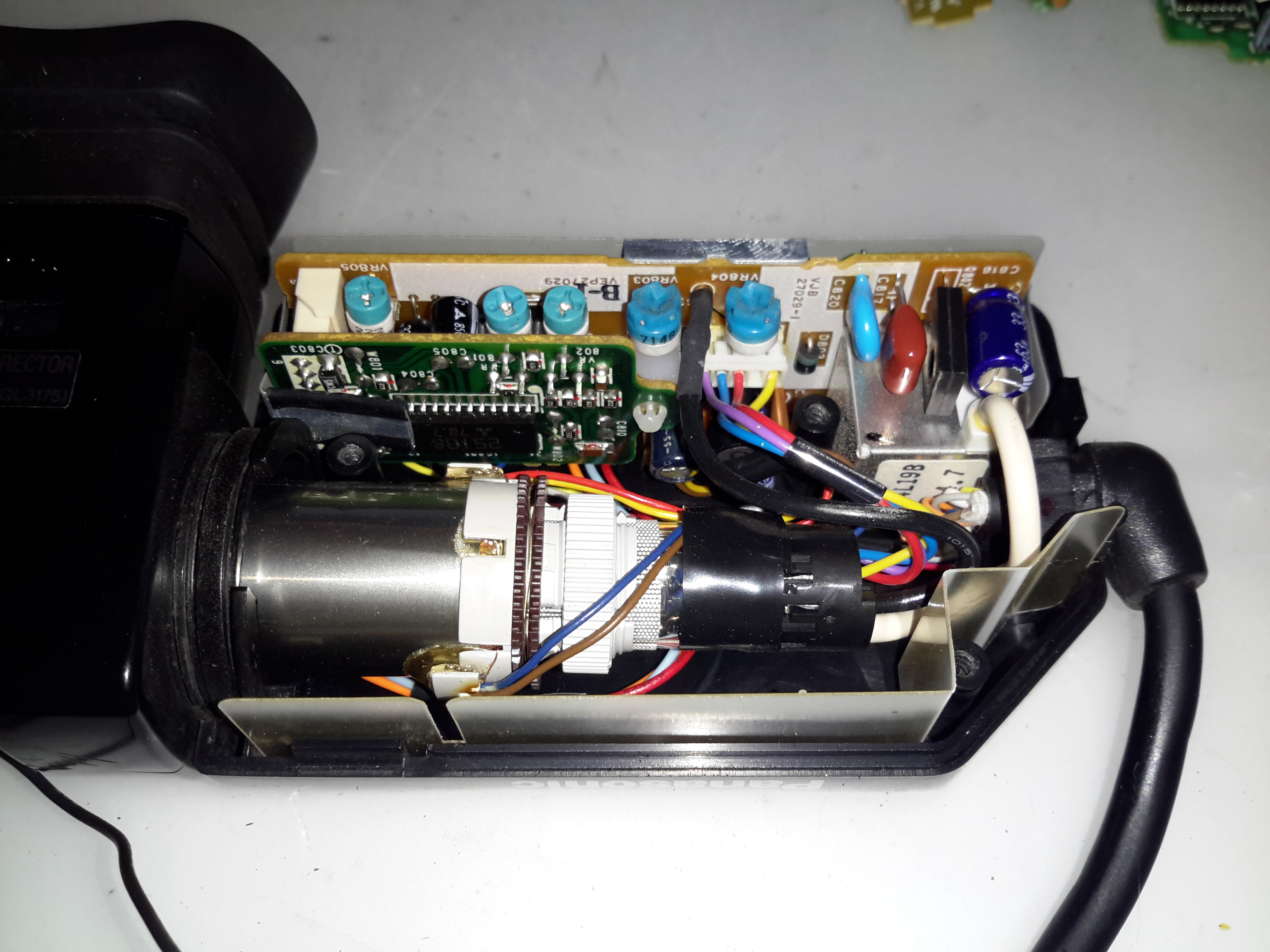
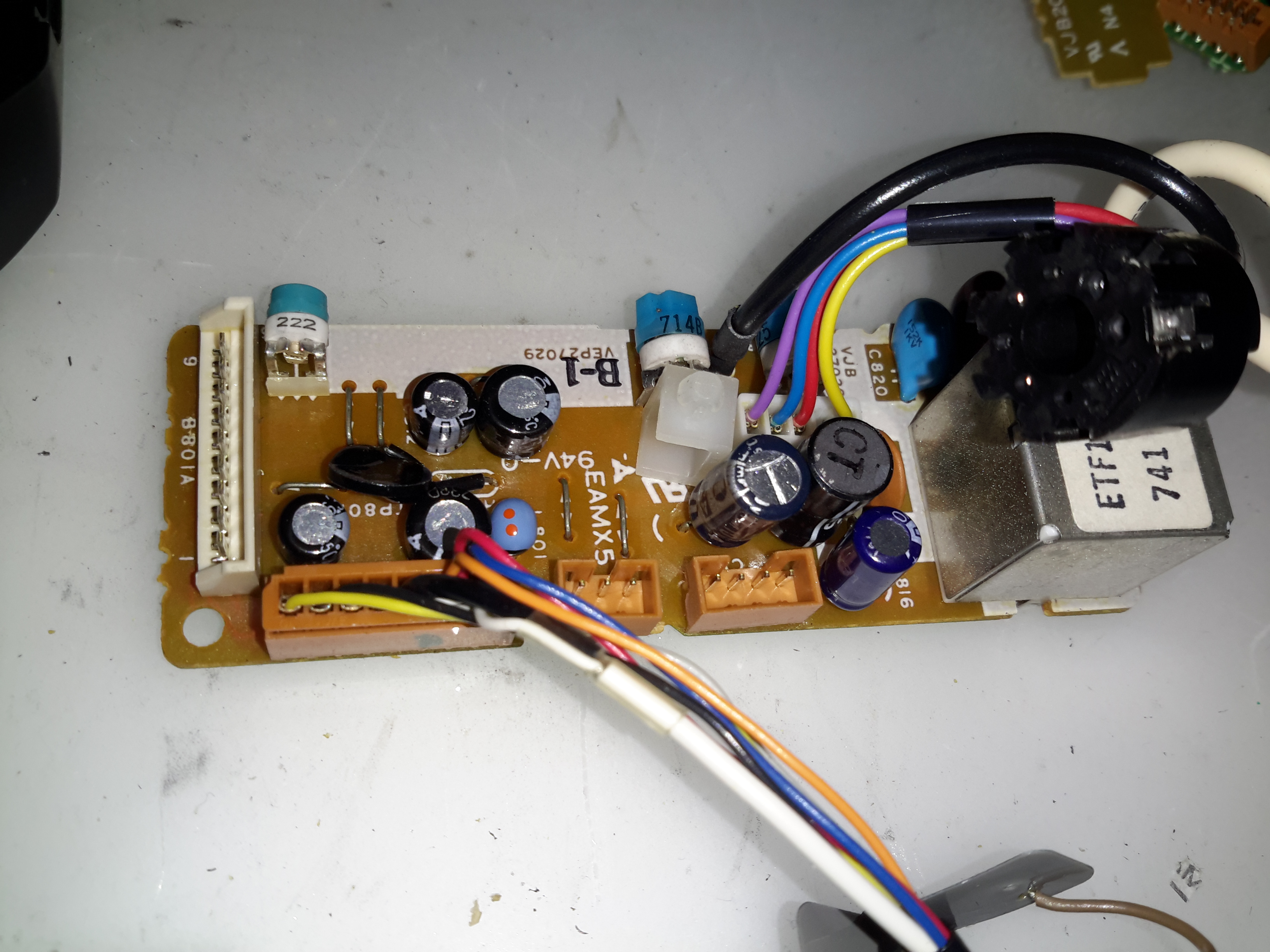
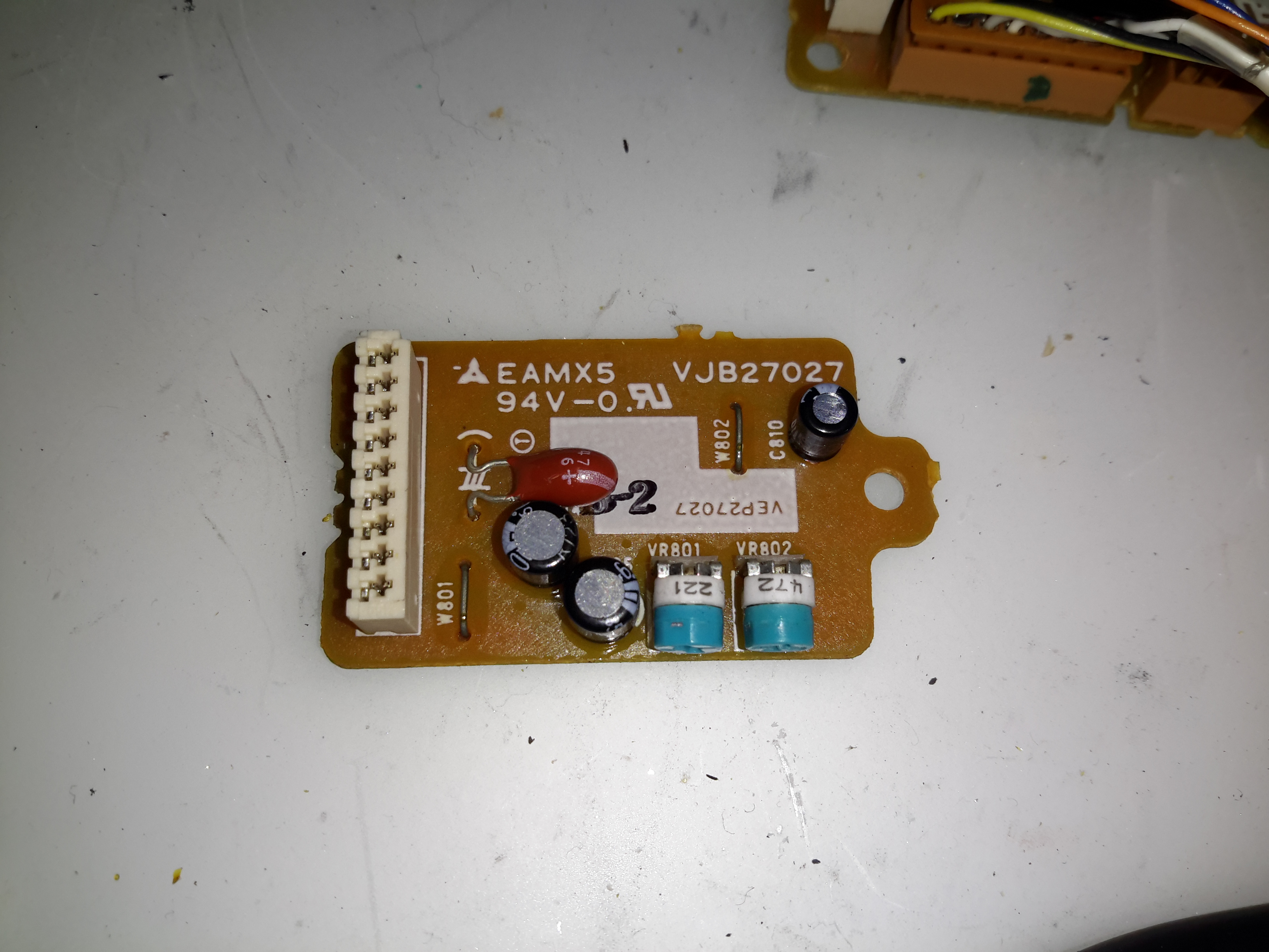
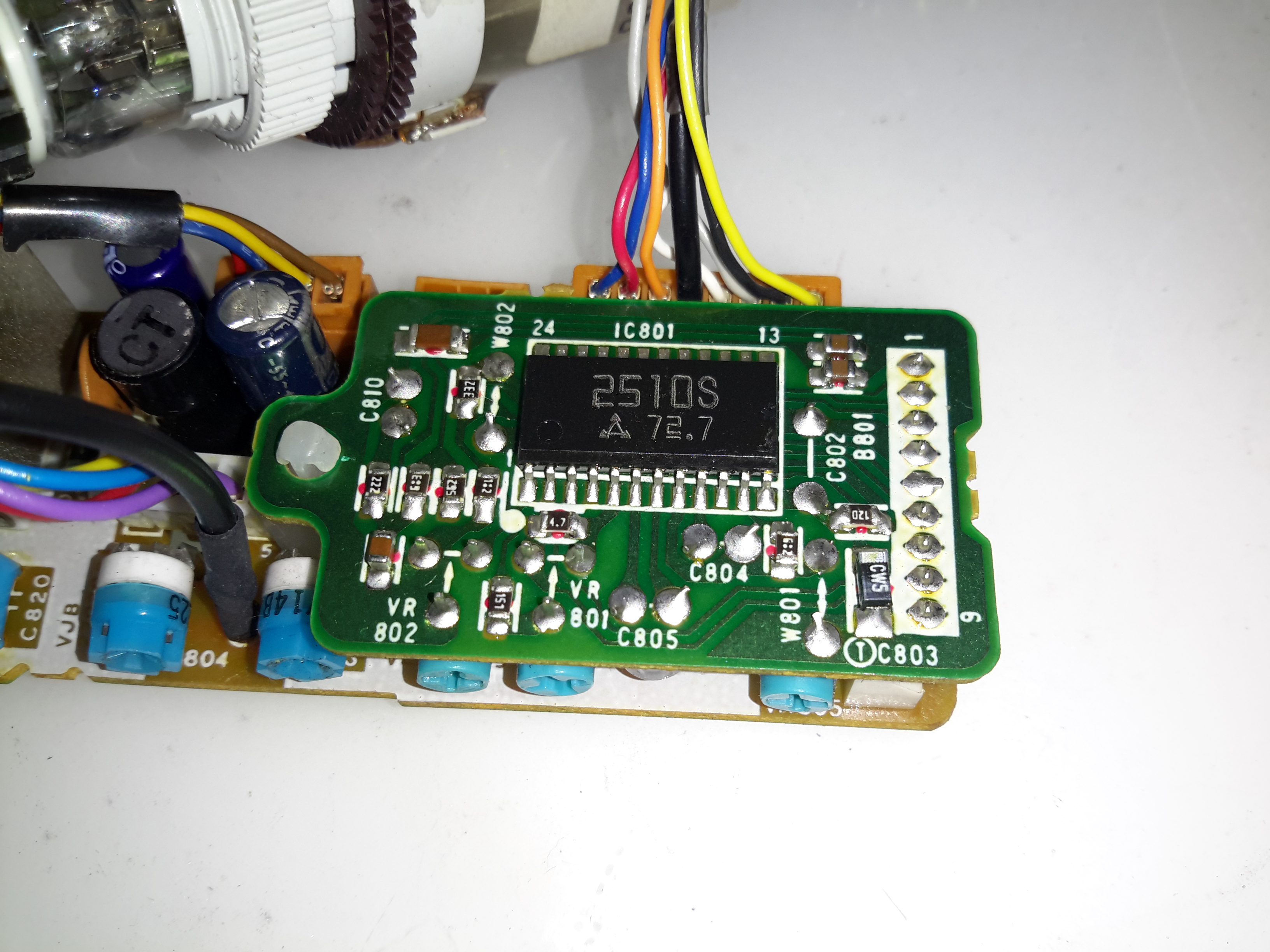
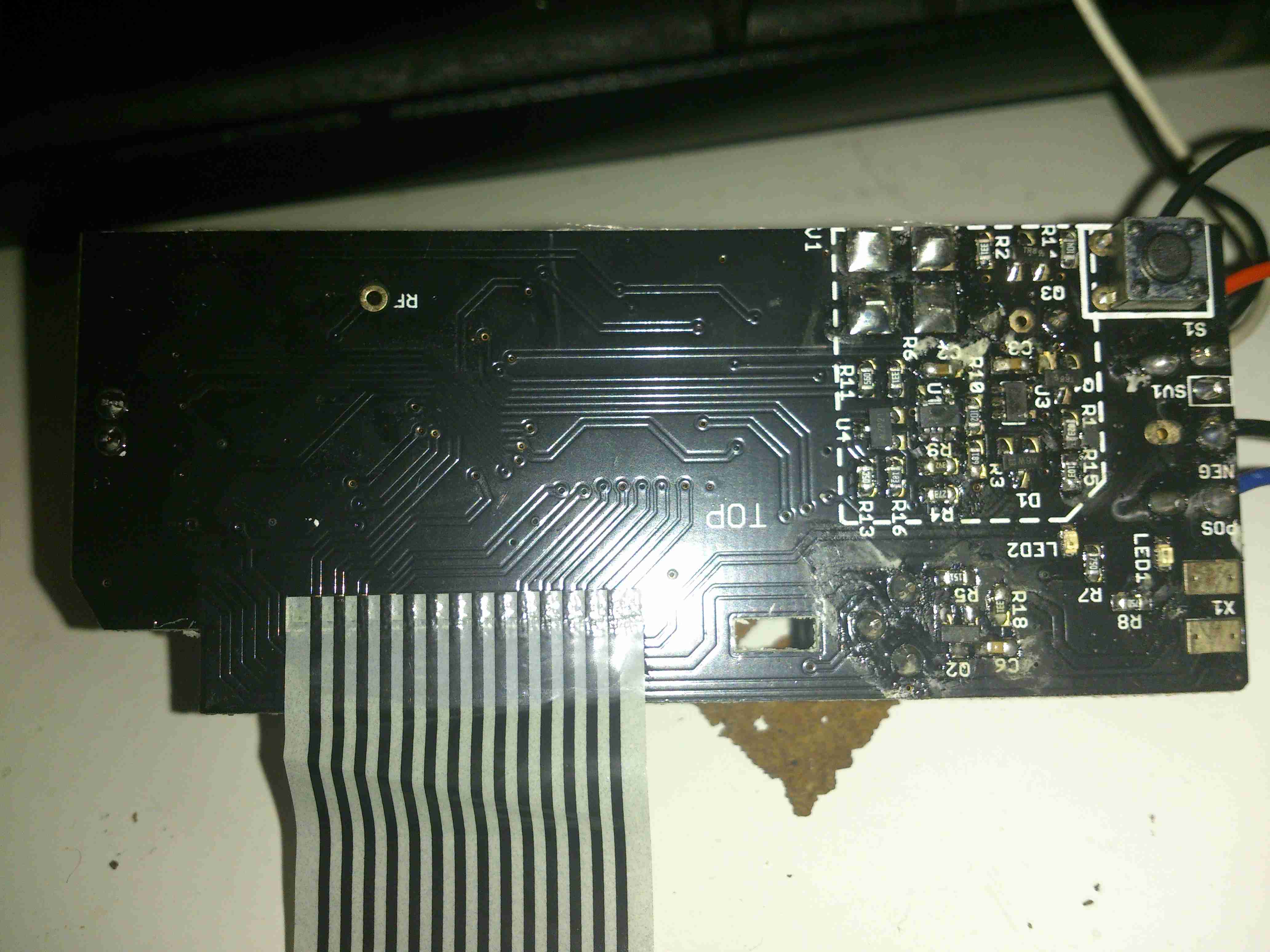
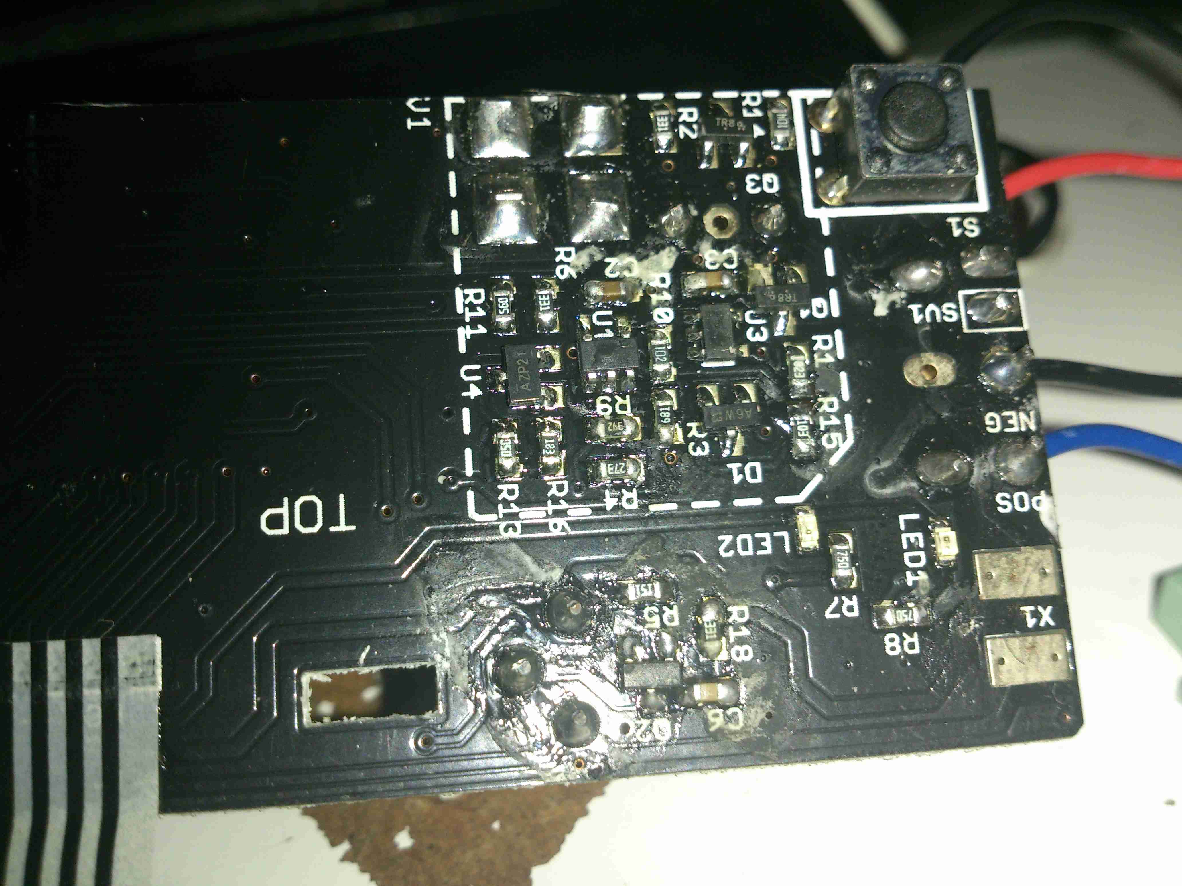
Removing some of the remaining covers exposes the bare video controls, and a small PCB just underneath covered in trimpots to set factory levels.

White Balance Filter Arm

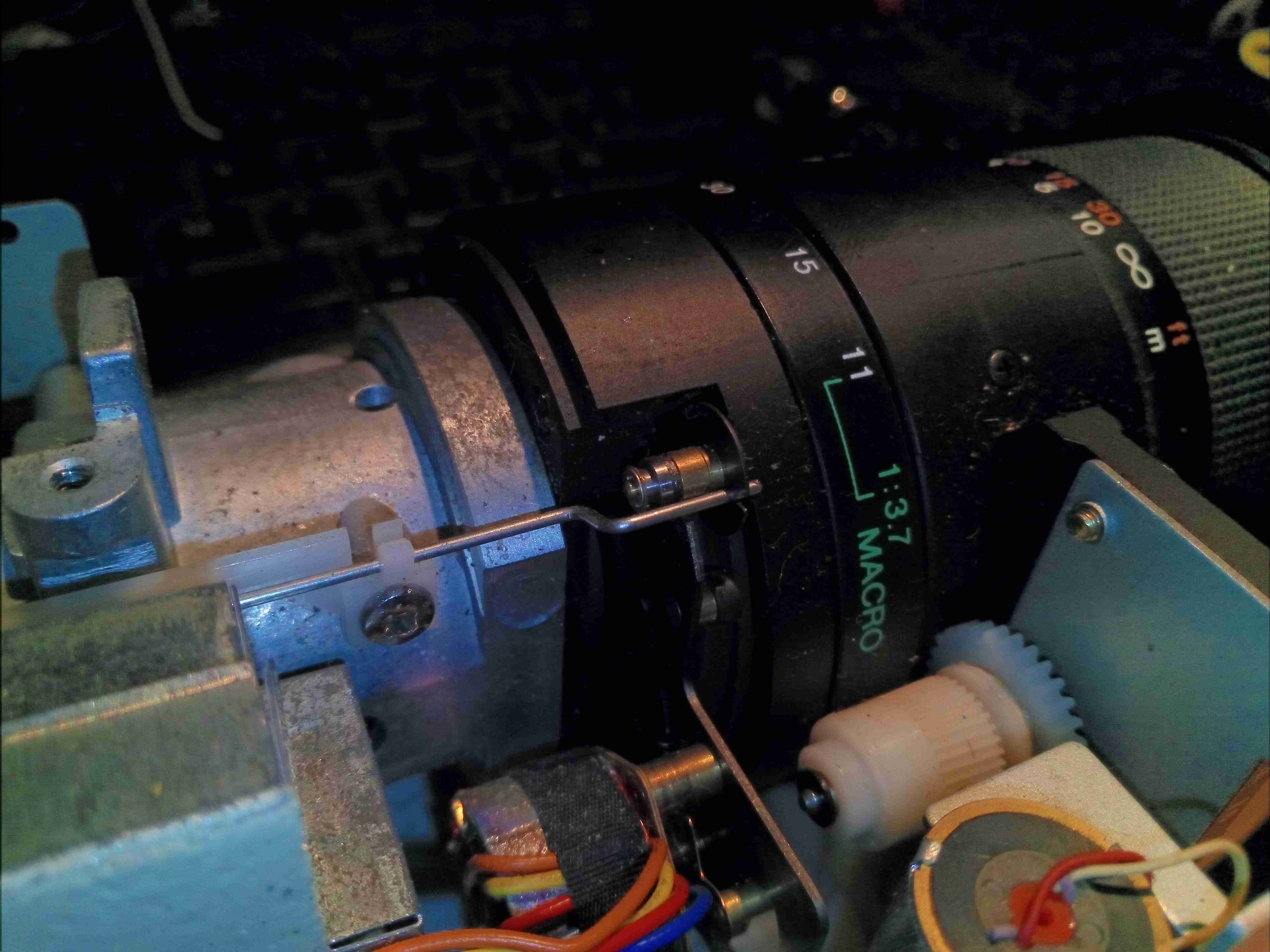
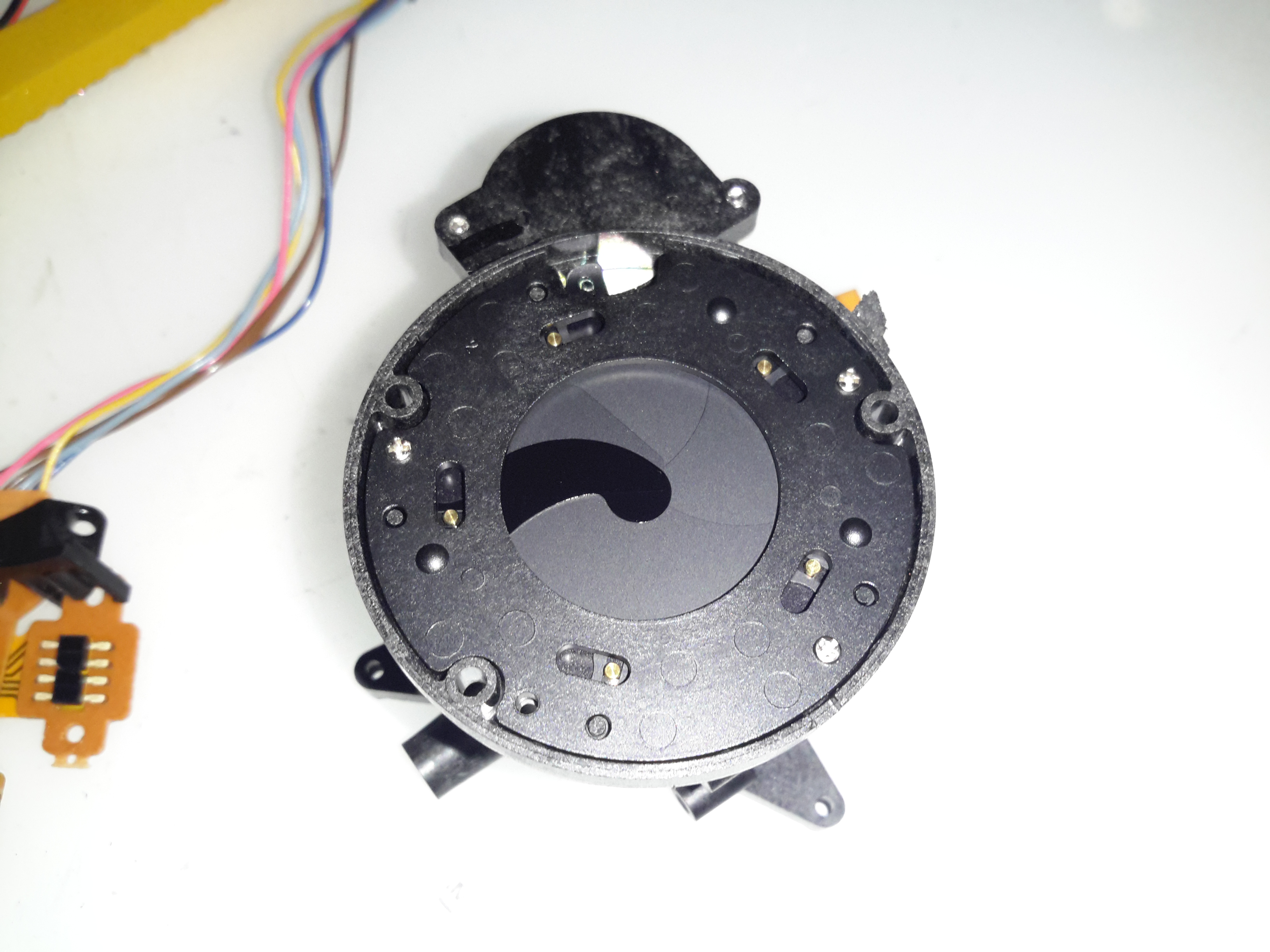
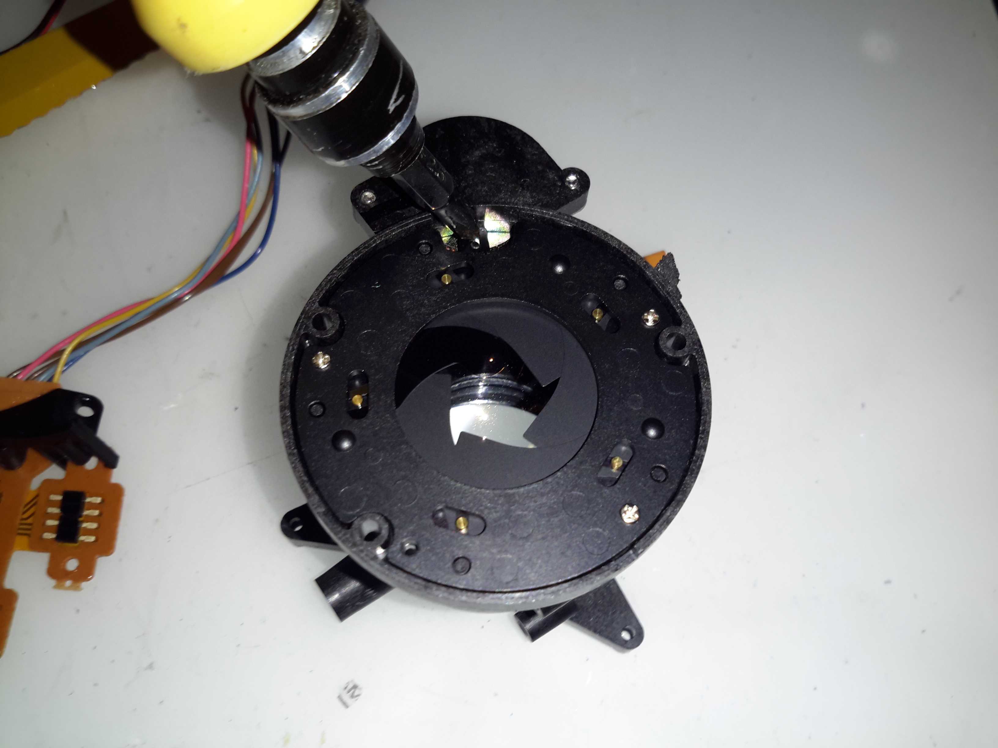
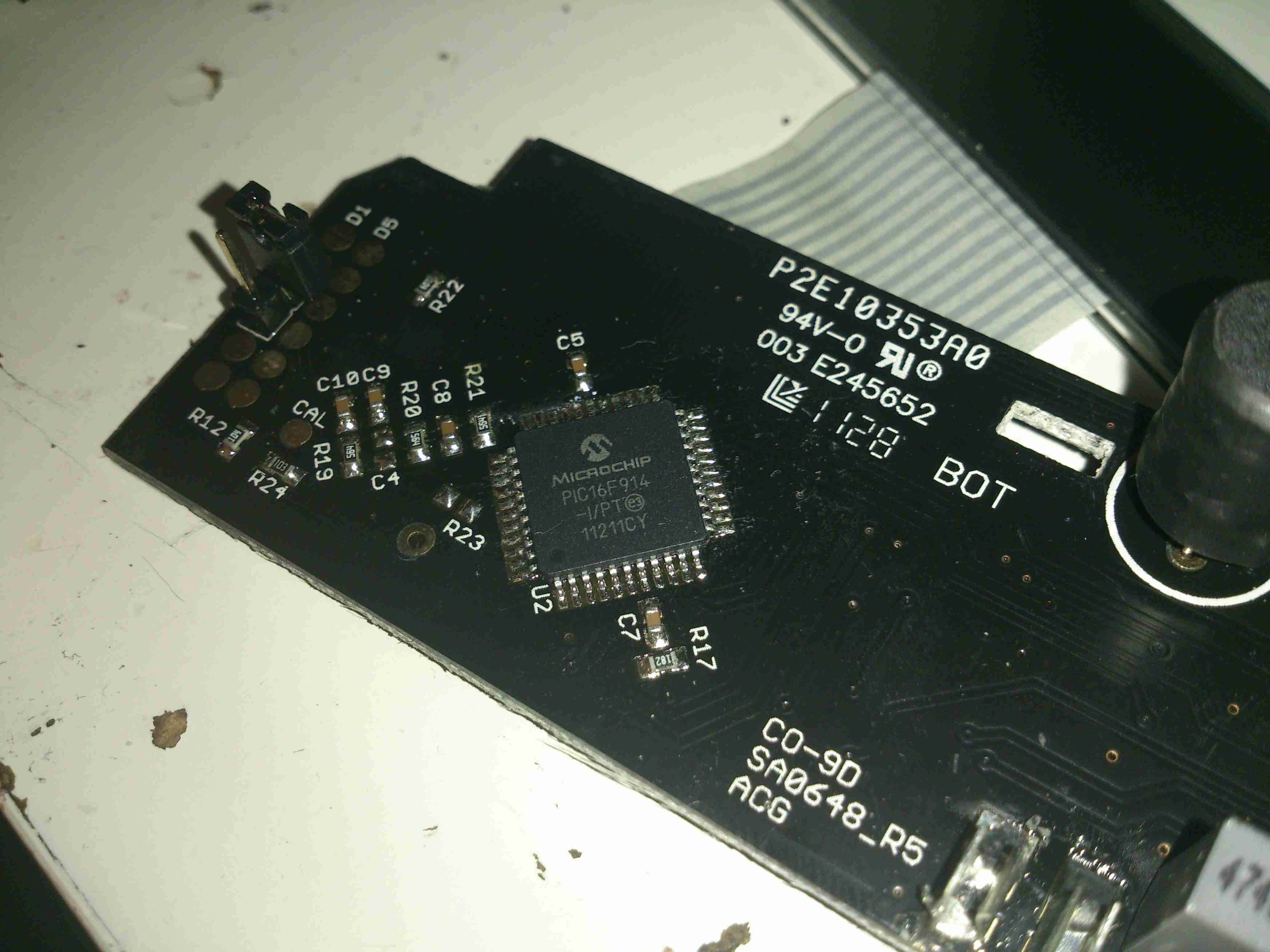
The white balance is partially electronic & partially mechanical. This lever actuates a filter inside the lens assrembly.

Remote Connector
Remote Connector

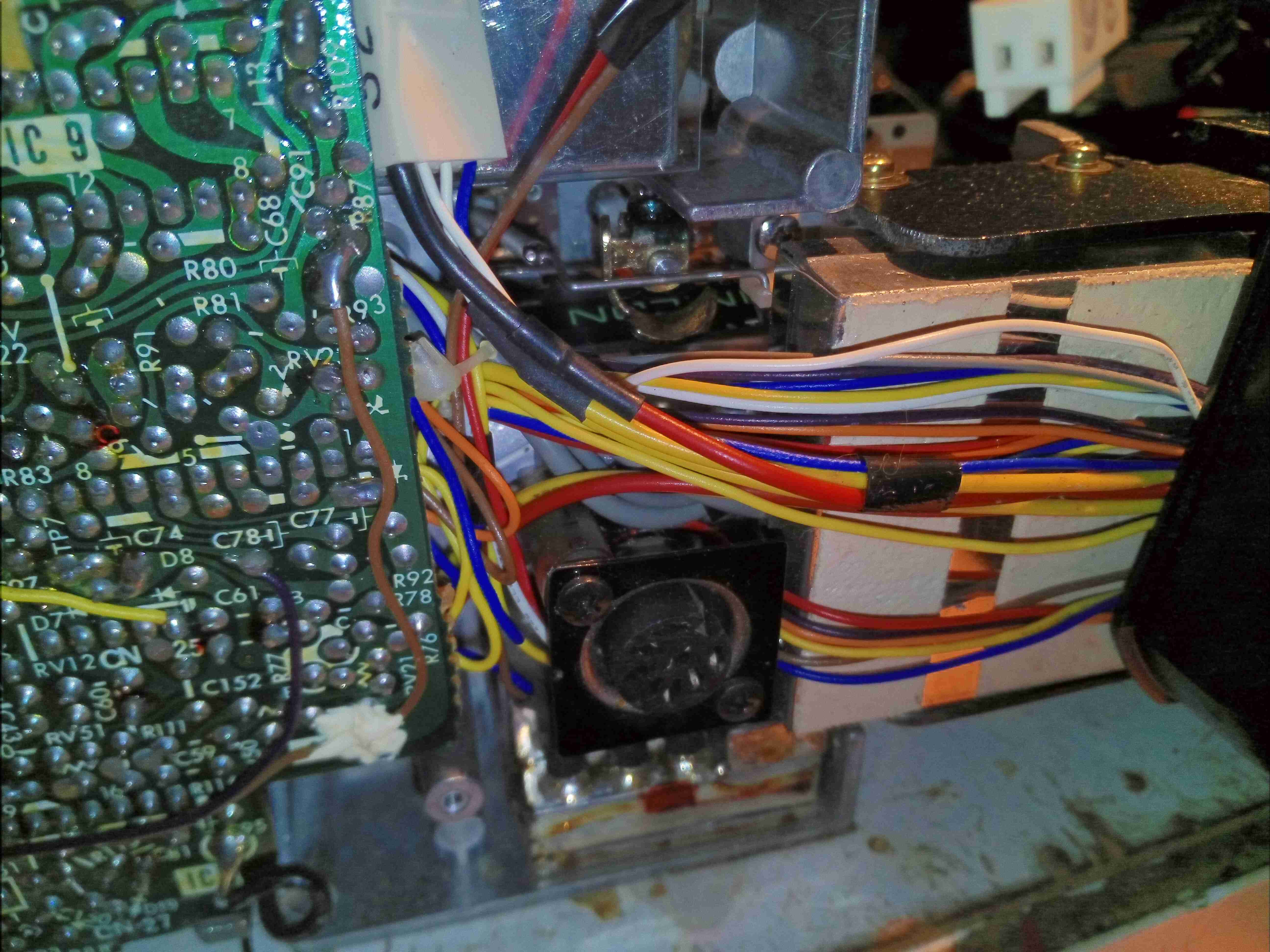
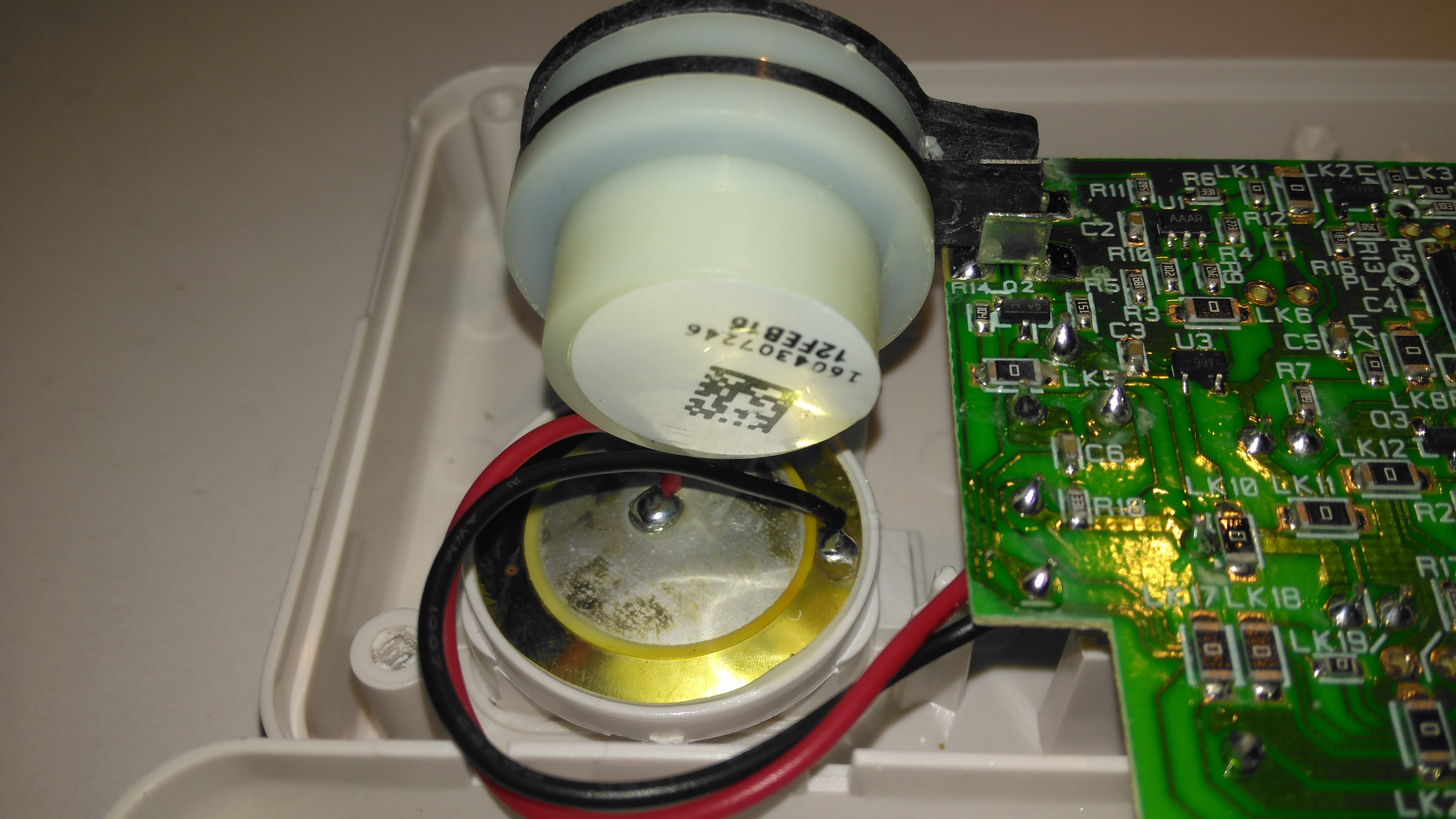
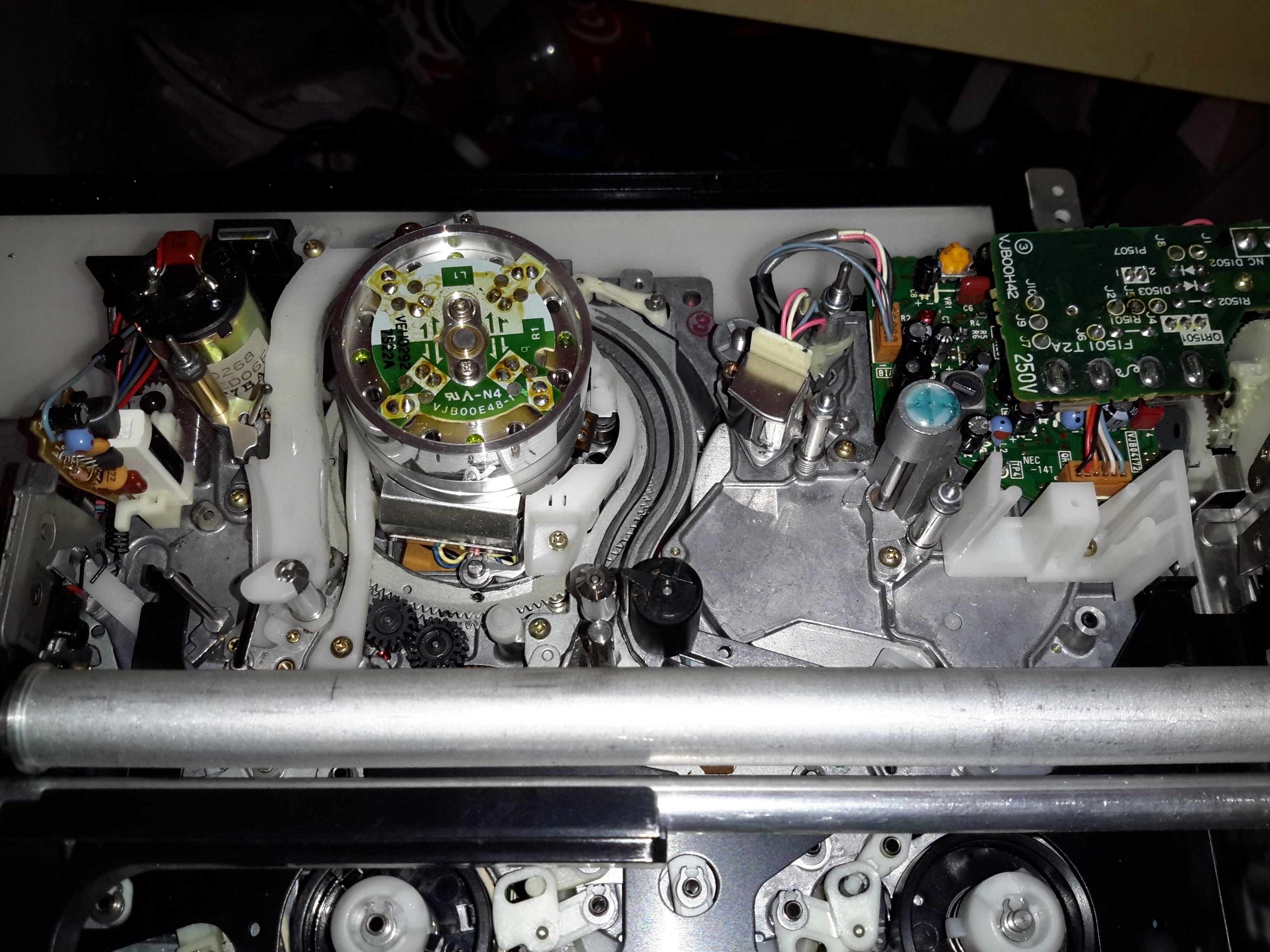
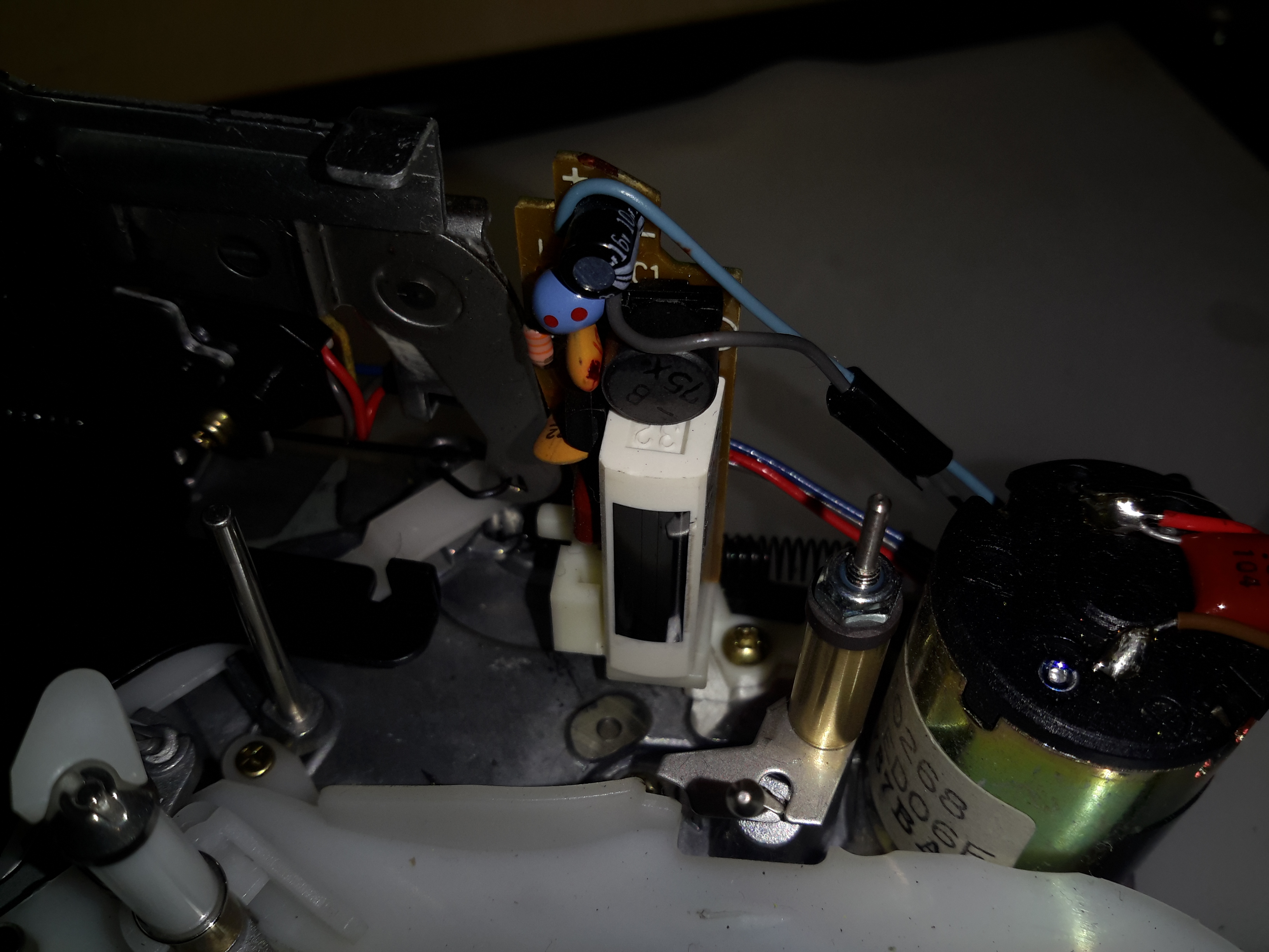
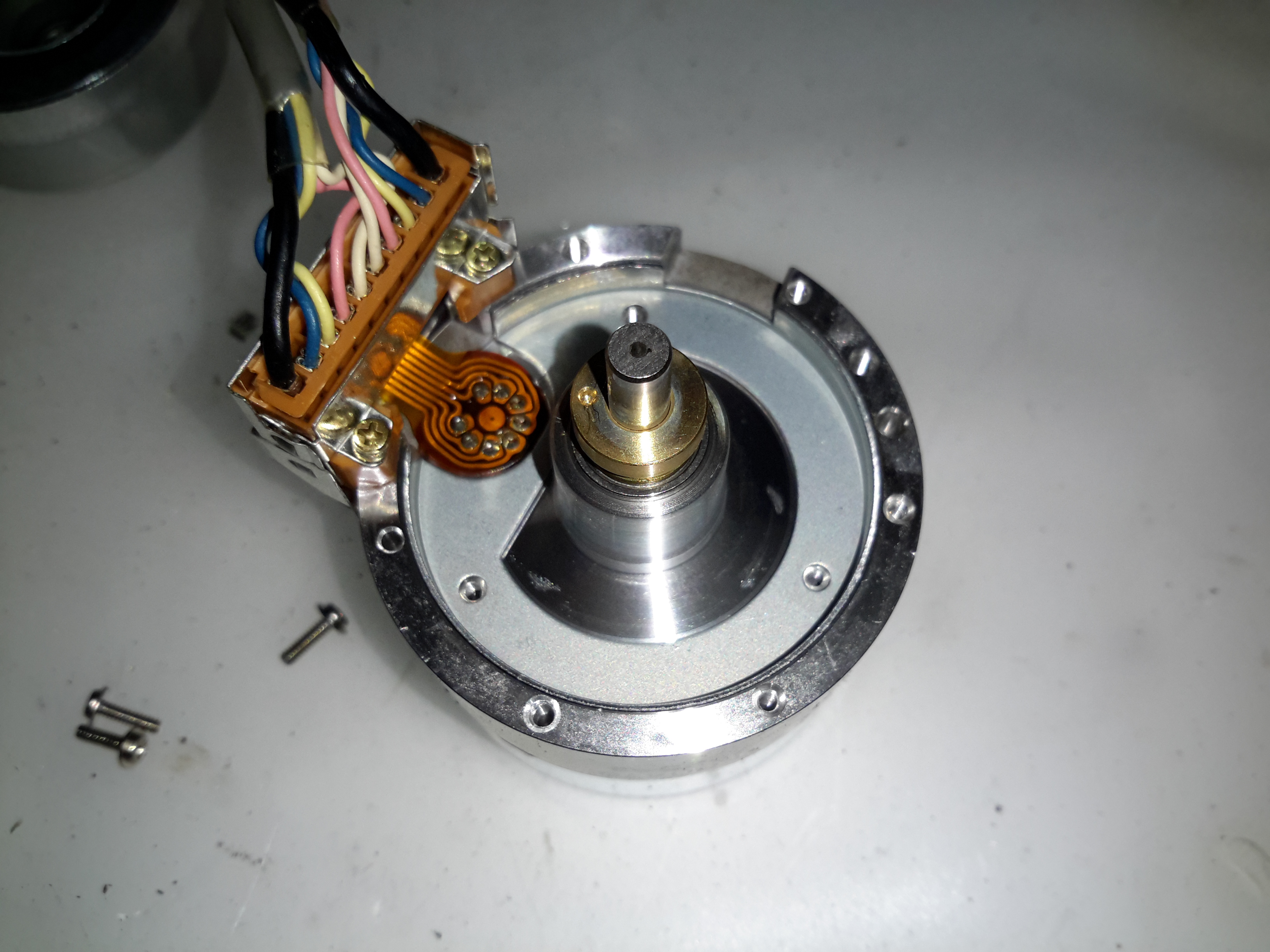
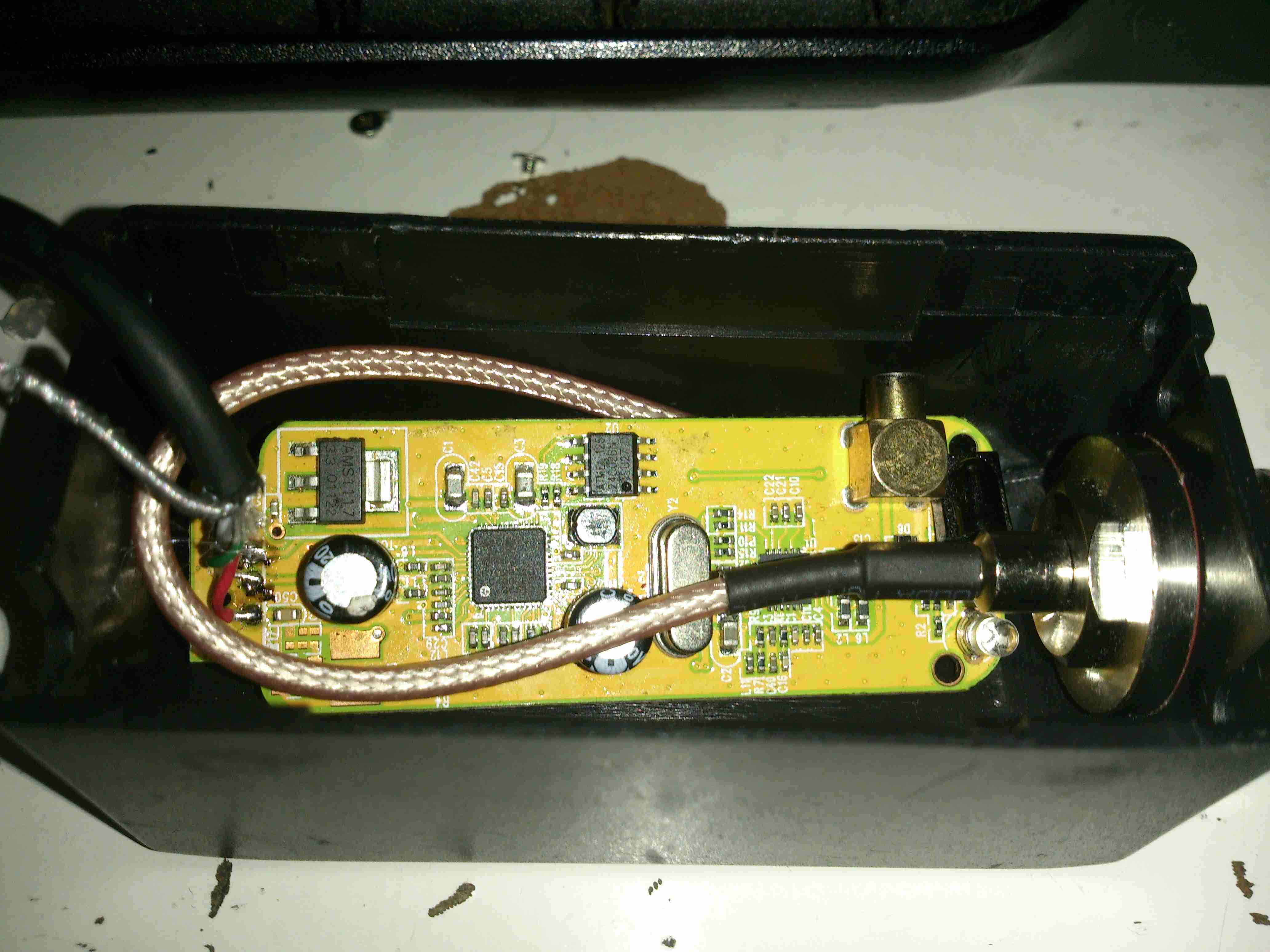
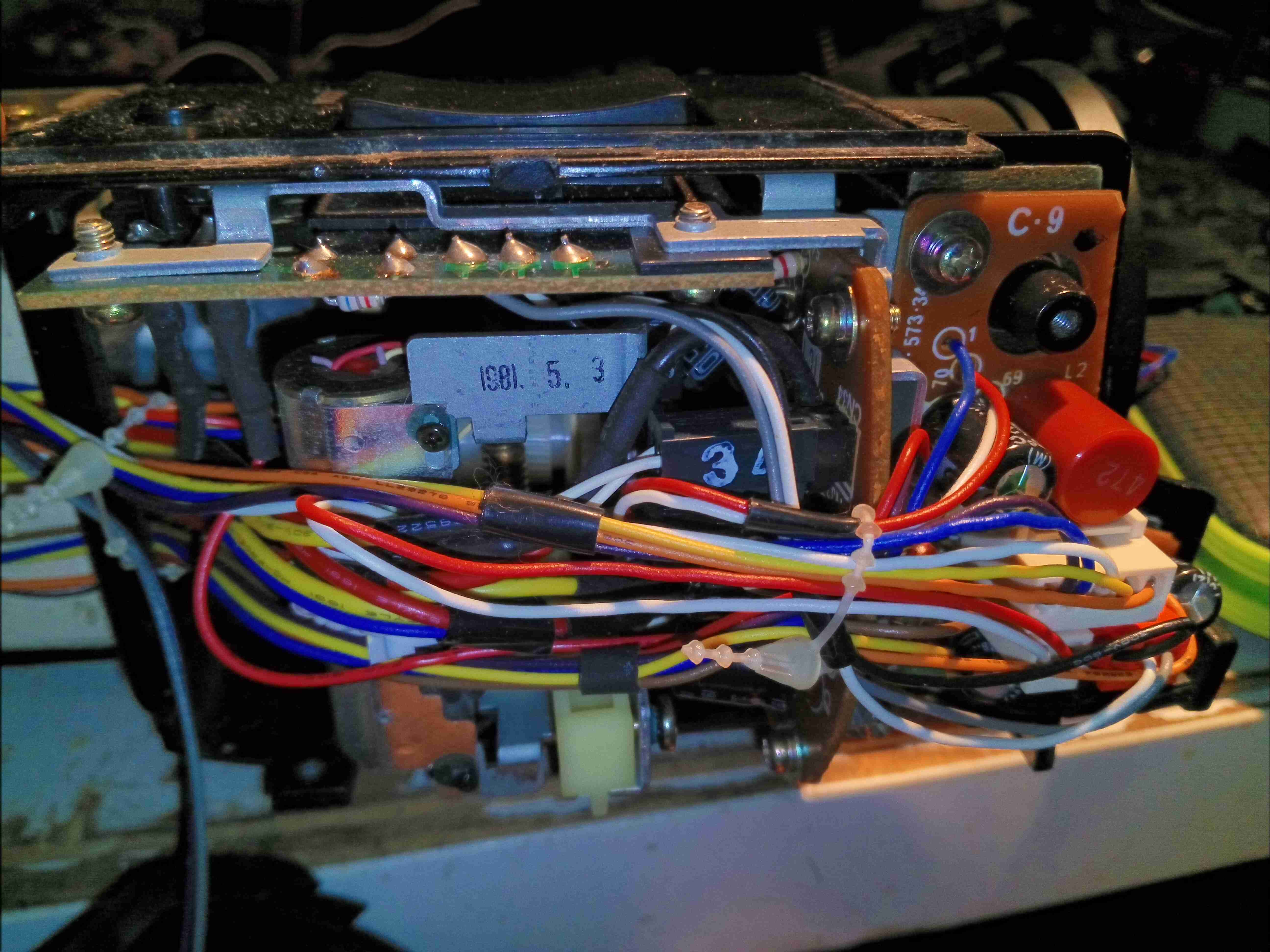
A DIN connector offers remote control ability. The large loom of wires disappearing off to the right is dealing with the zoom mechanism & the onboard microphone amplifier. Just under the DIN connector hides the system power supply, inside a soldered can. The can under the white tape is the head end amplifier for the Trinicon video tube.

Trinicon Mount
Trinicon Mount

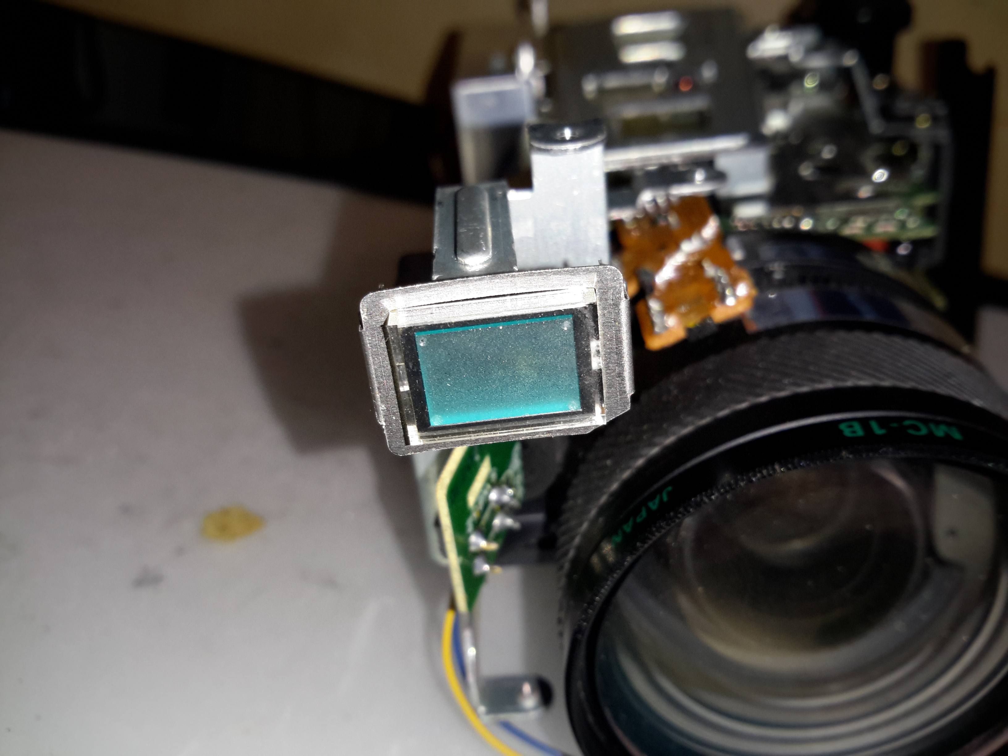
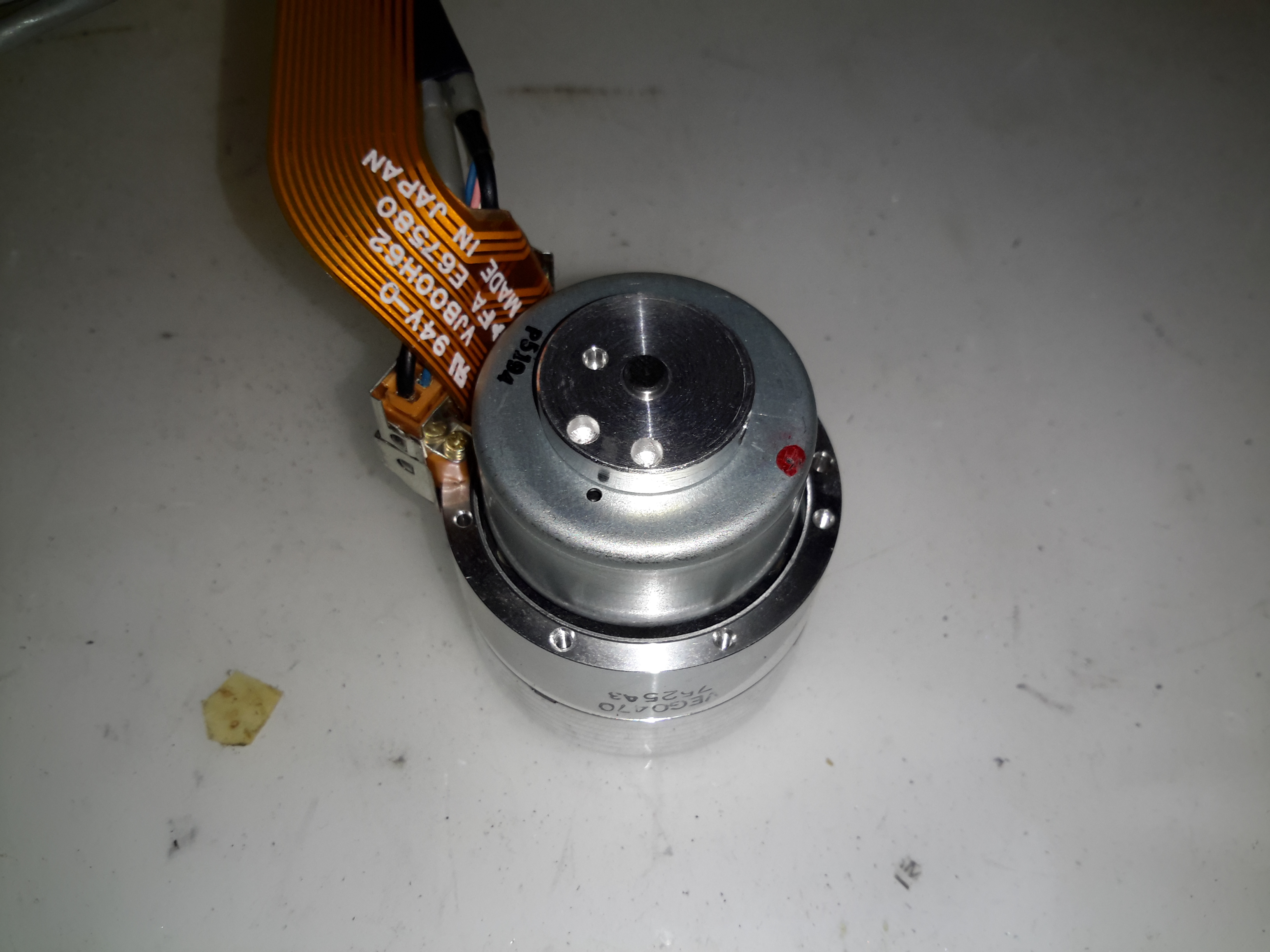
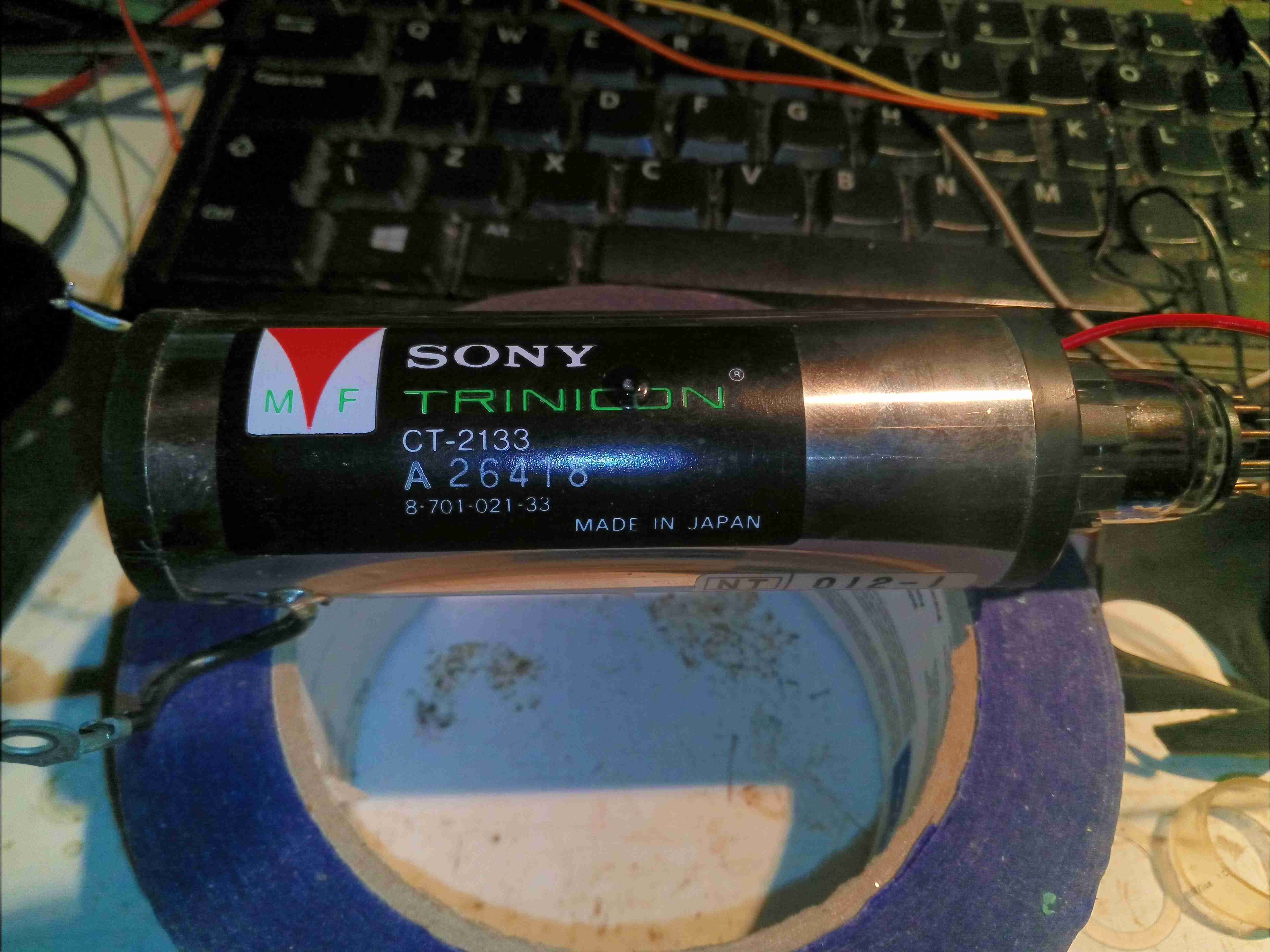
Hiding in the centre of the camera inside the casting is the Trinicon tube assembly itself. The label can just be seen here.

Camera Internals 1
Camera Internals 1

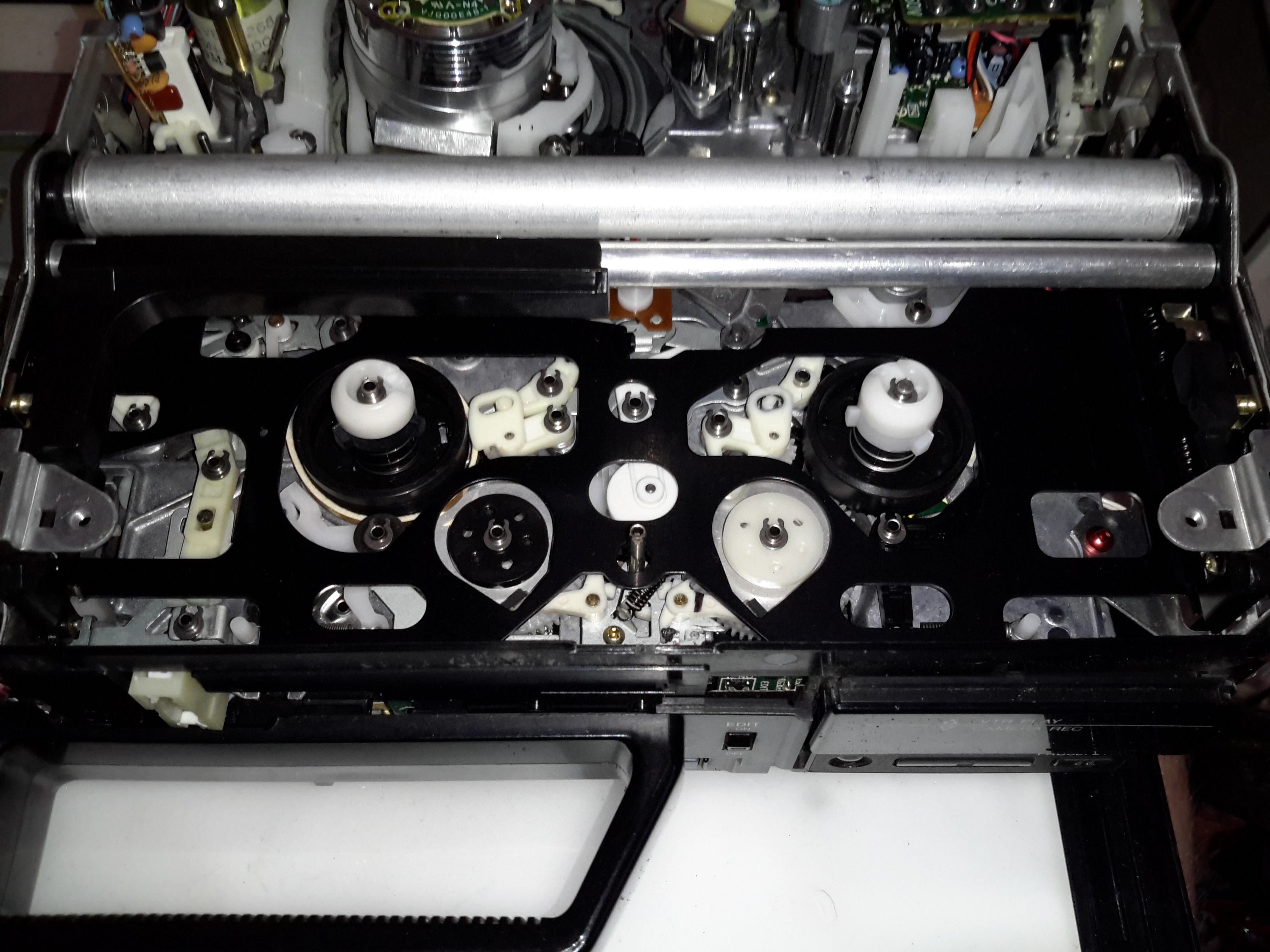
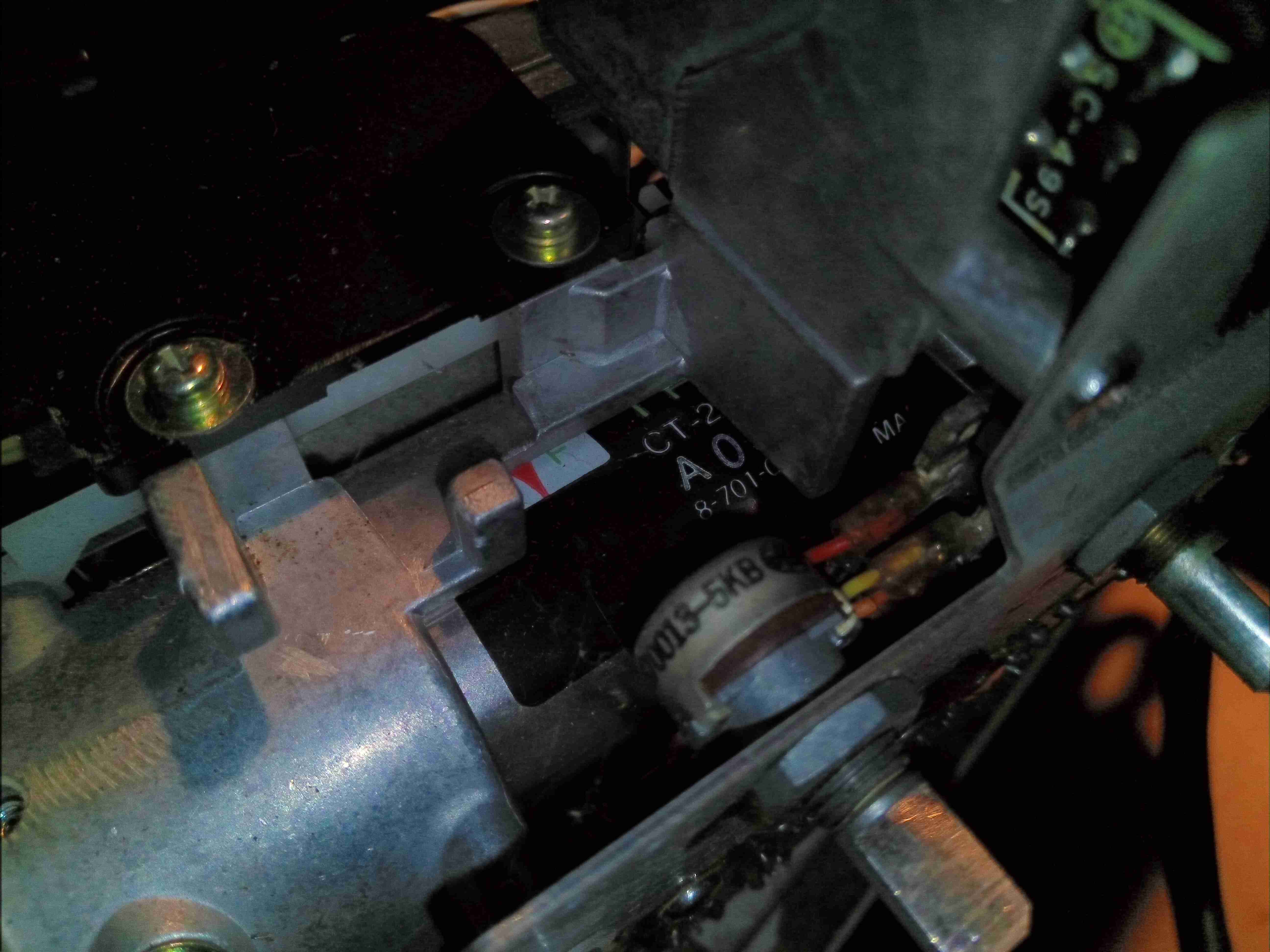
As is typical of 1980’s electronic design, the main boards swing down & are designed to slot into the base casting folded out for repairs. Internally the unit is a rat’s nest of wiring loom. There’s also another shielding can in here nestled between the boards – this is the video sync generator circuit.

Camera Internals 2
Camera Internals 2

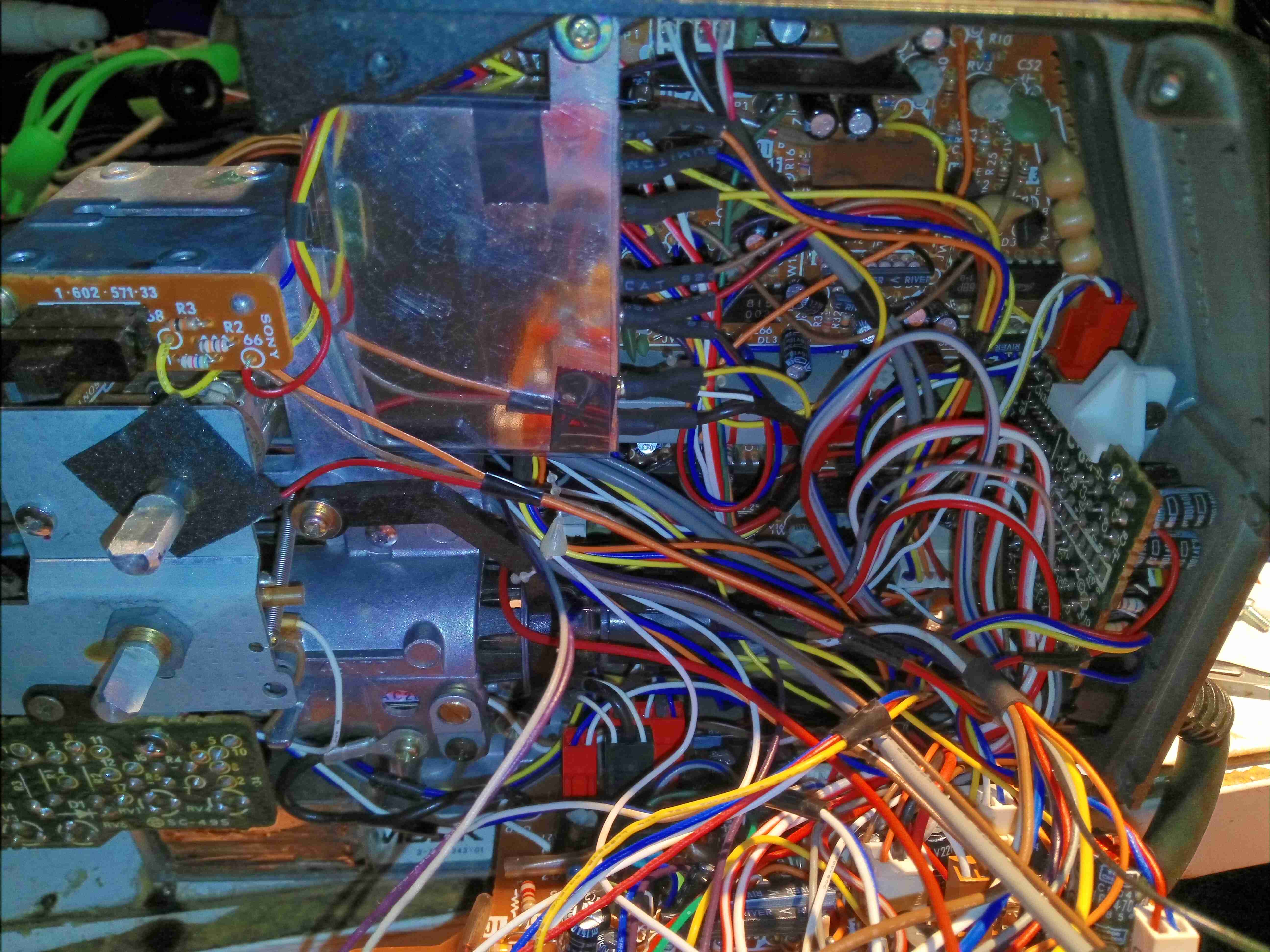
The other side gives a better view of the video sync generator can. I’ll dive into the individual modules later on.

Lens Zoom Assembly
Lens Zoom Assembly

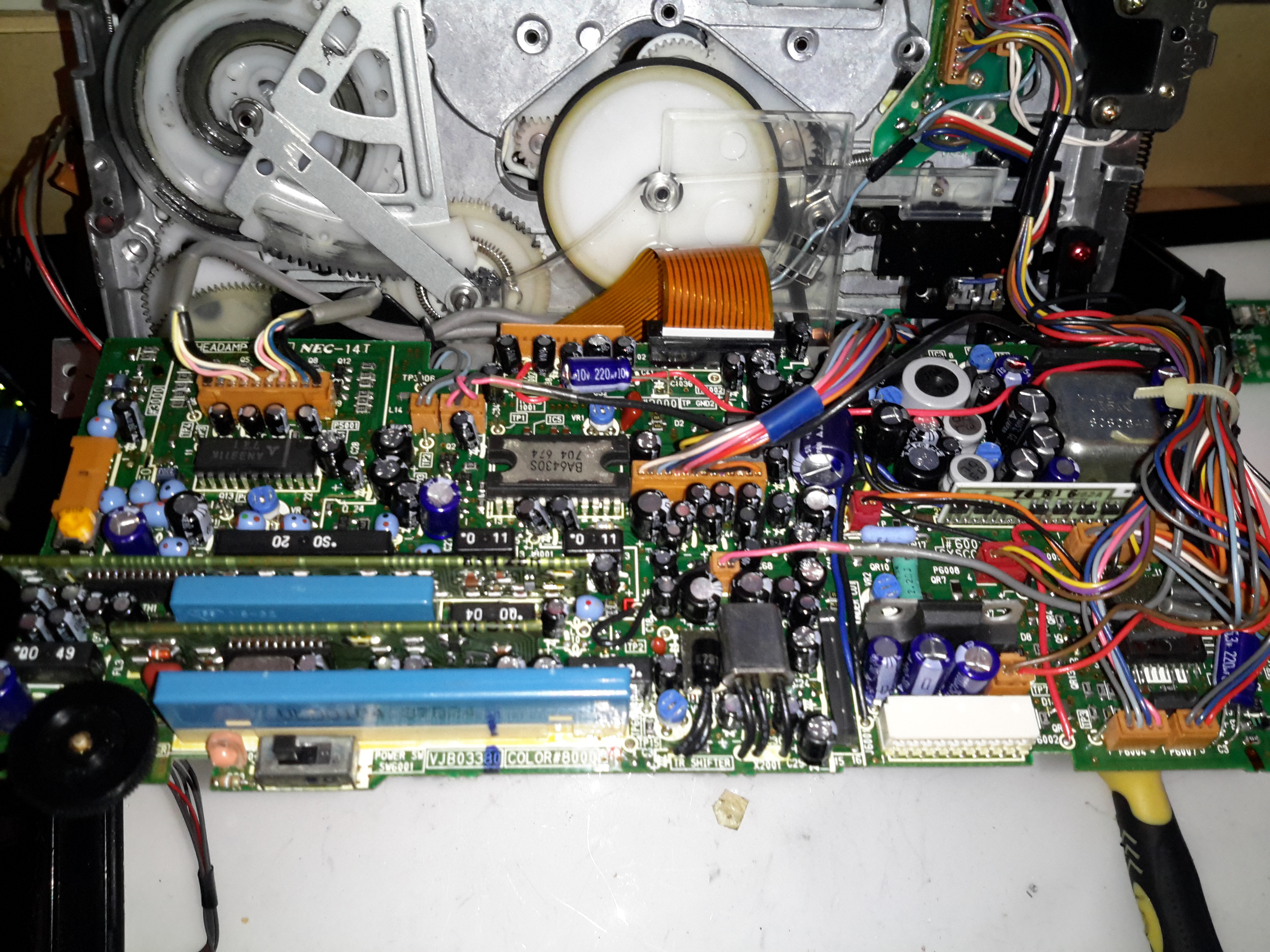
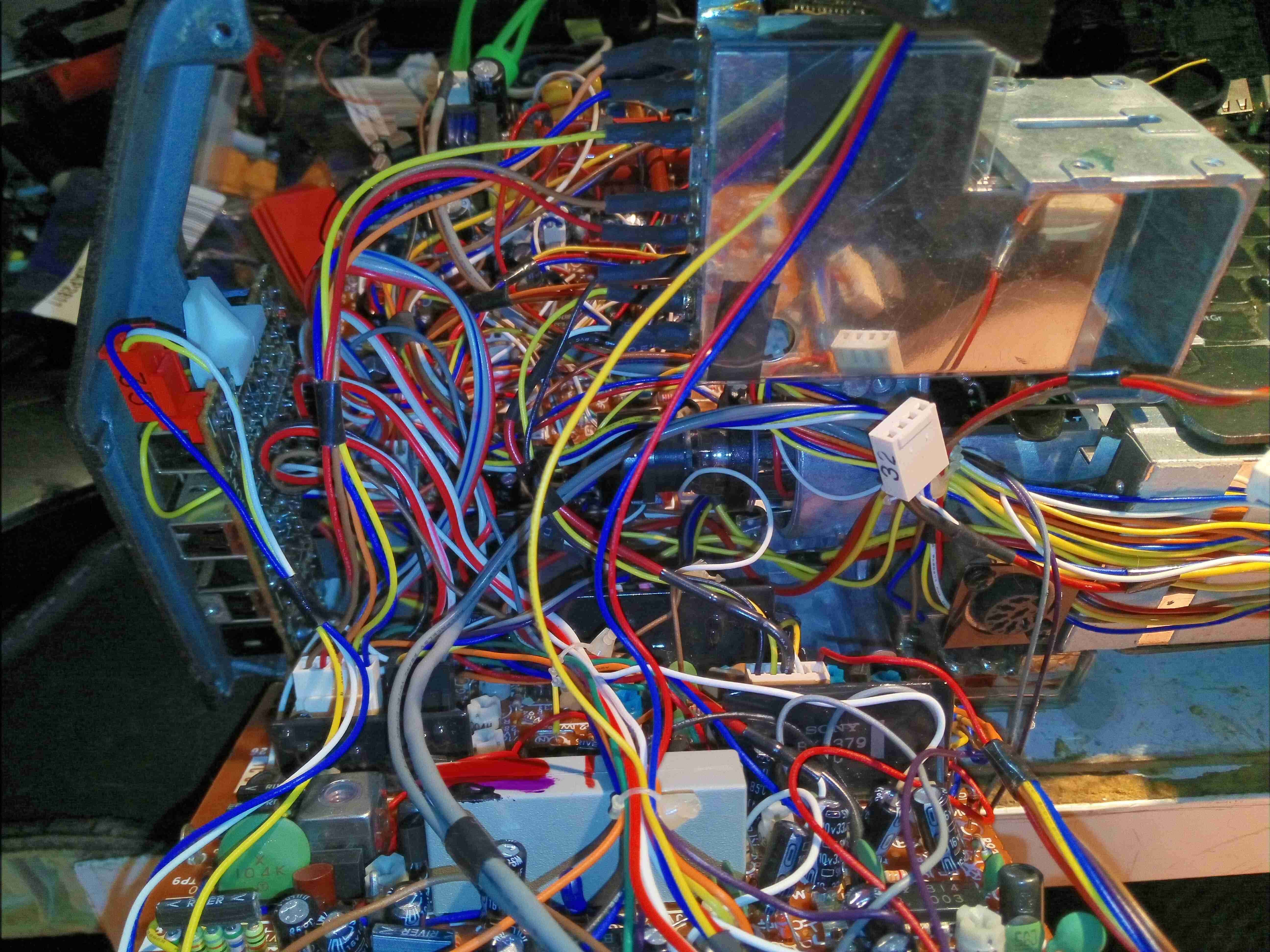
Under the remaining side cover is the zoom assembly & microphone amplifier board. More massive wiring loom hides within.

Video Sync Generator

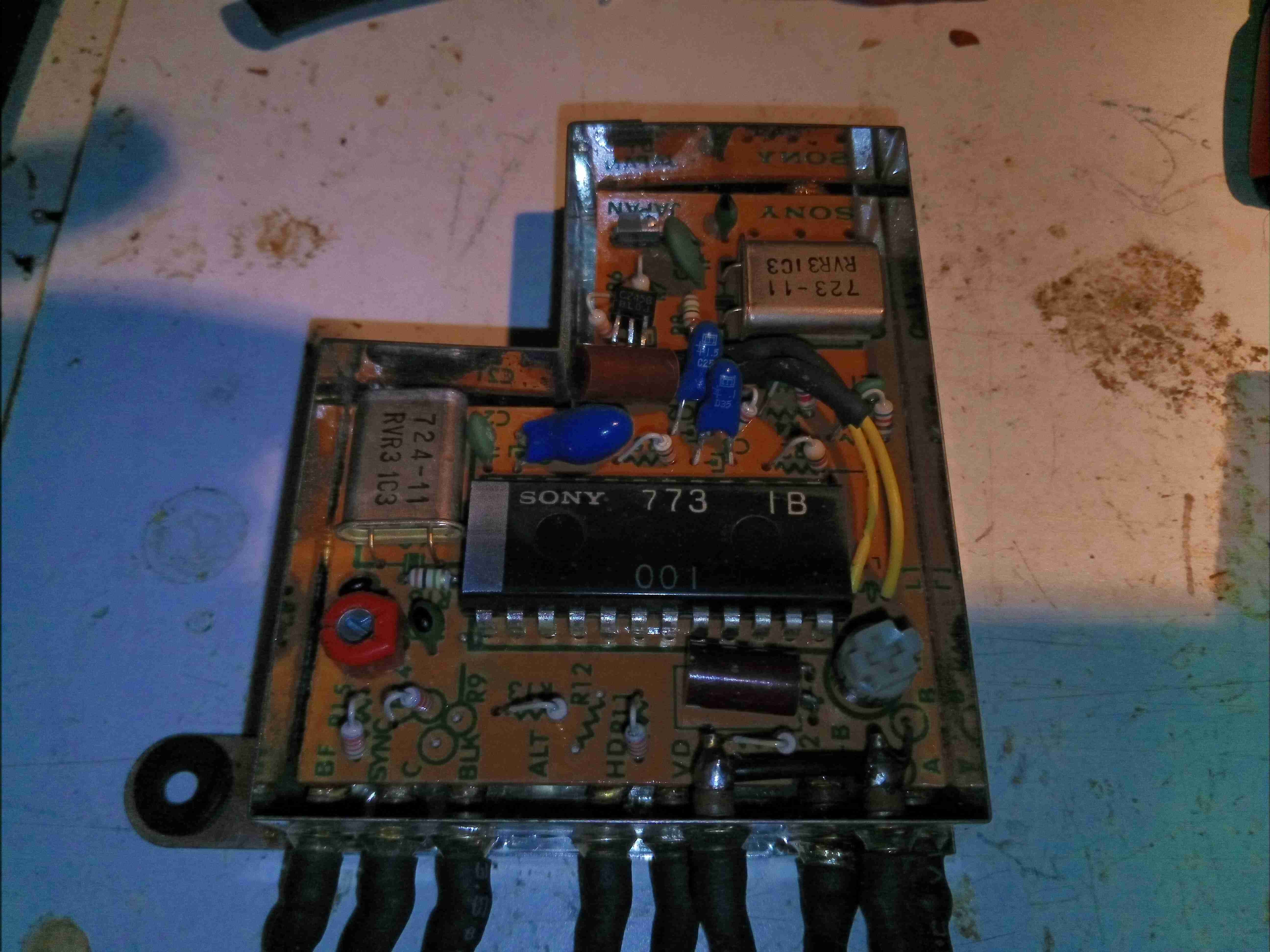
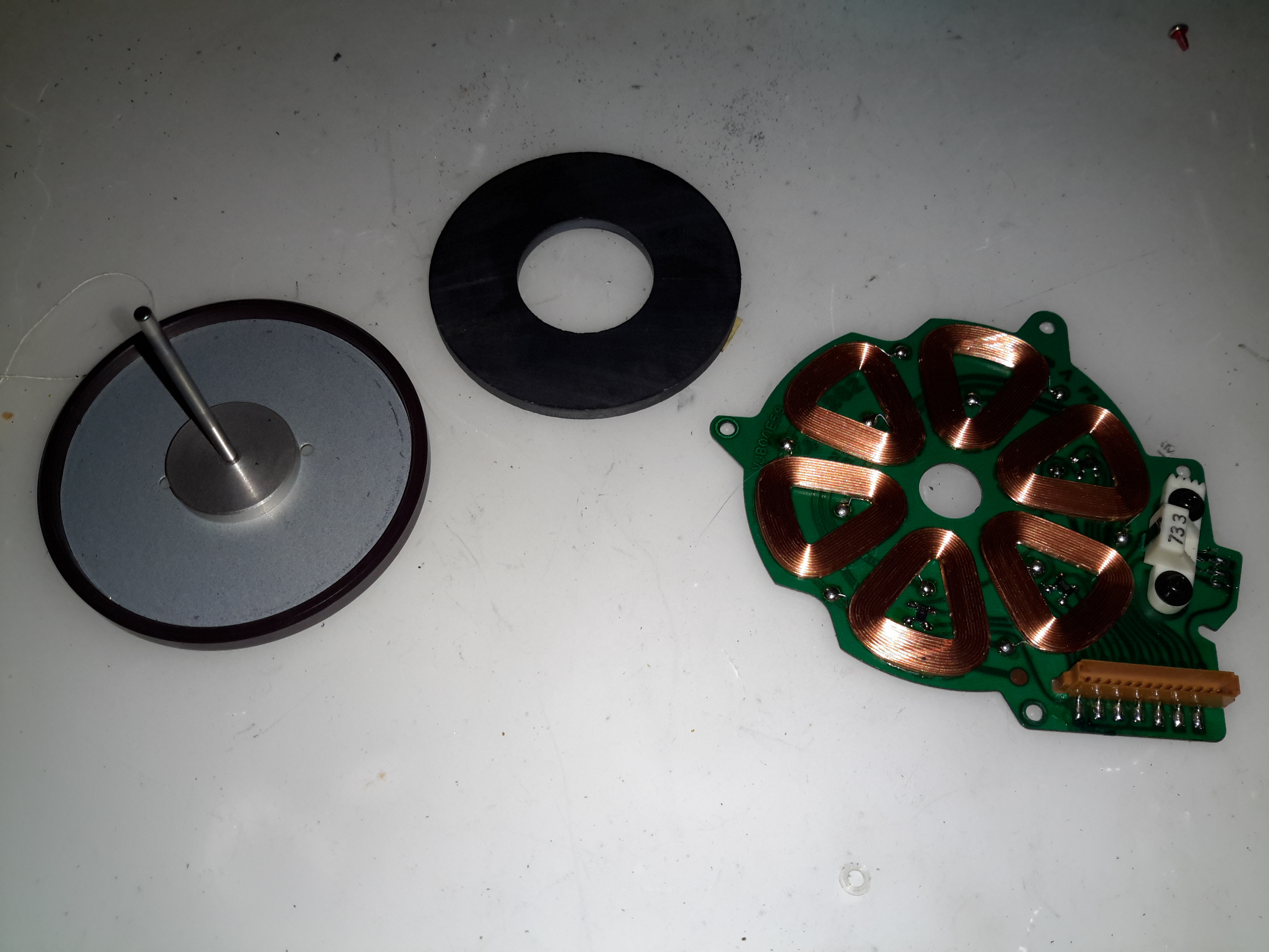
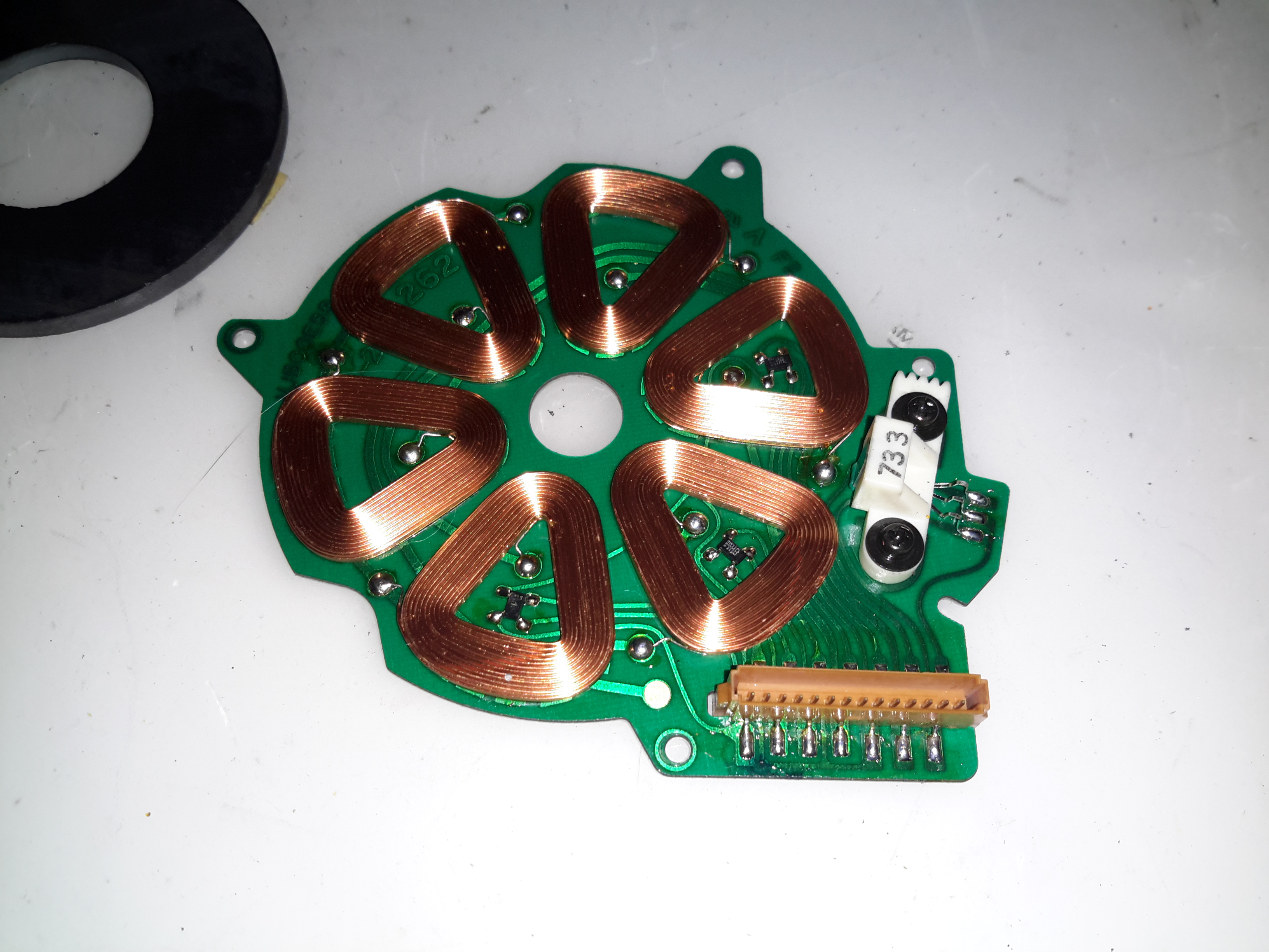
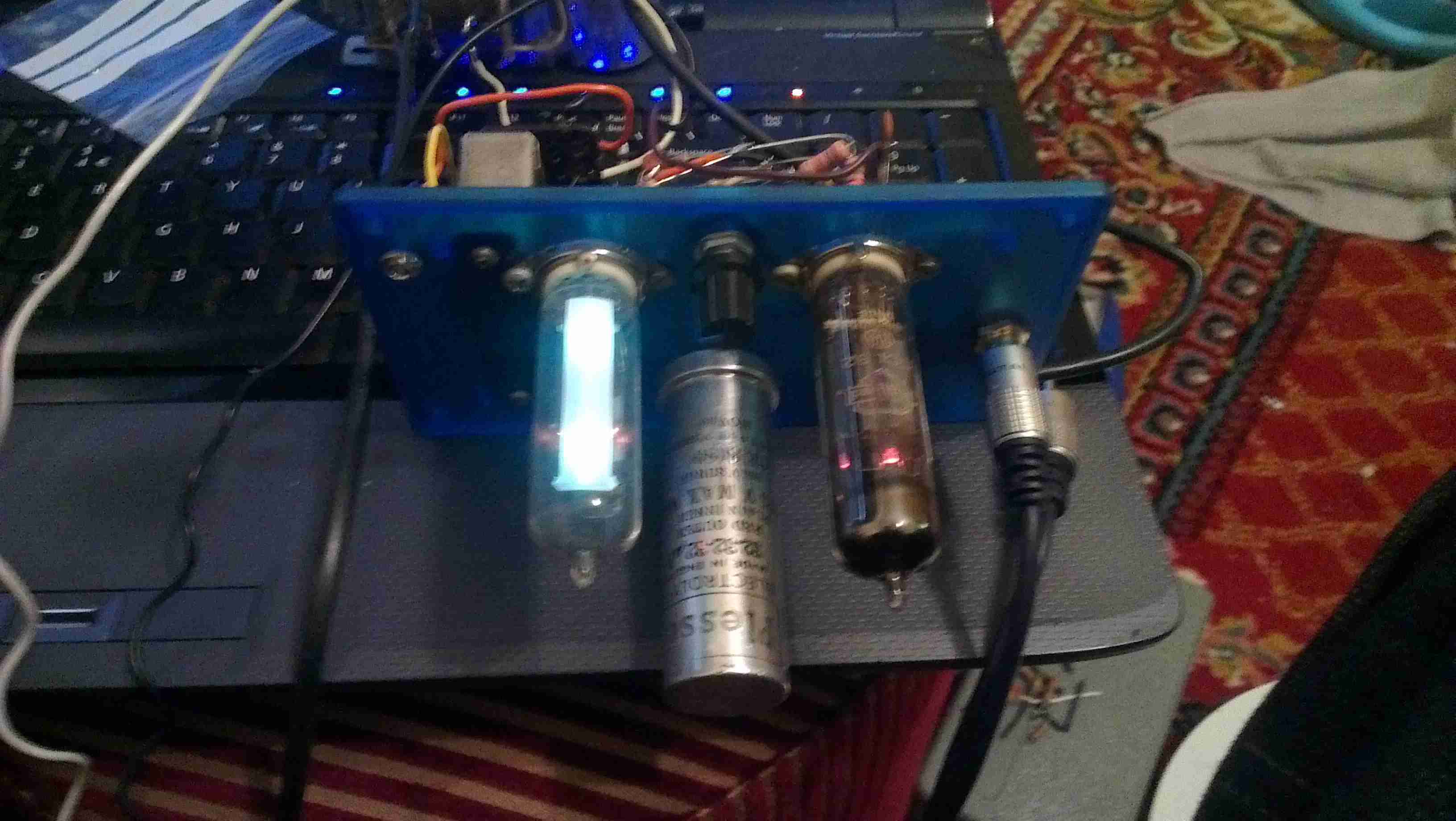
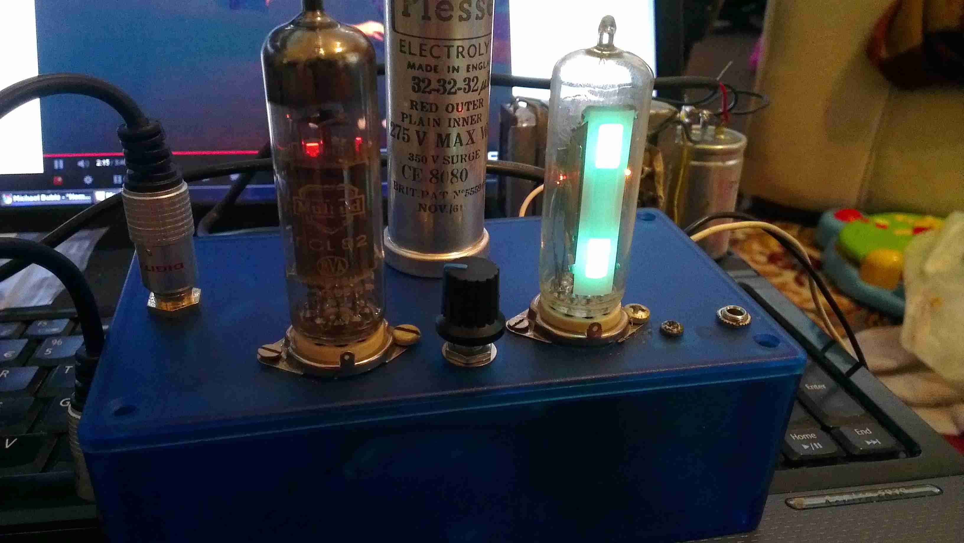
The video sync generator is pretty sparse inside, just a large Sony CX773 Sync Generator IC, with a pair of crystals. There are a couple of adjustments in here for video sync frequencies.

Head End Amplifier
Head End Amplifier

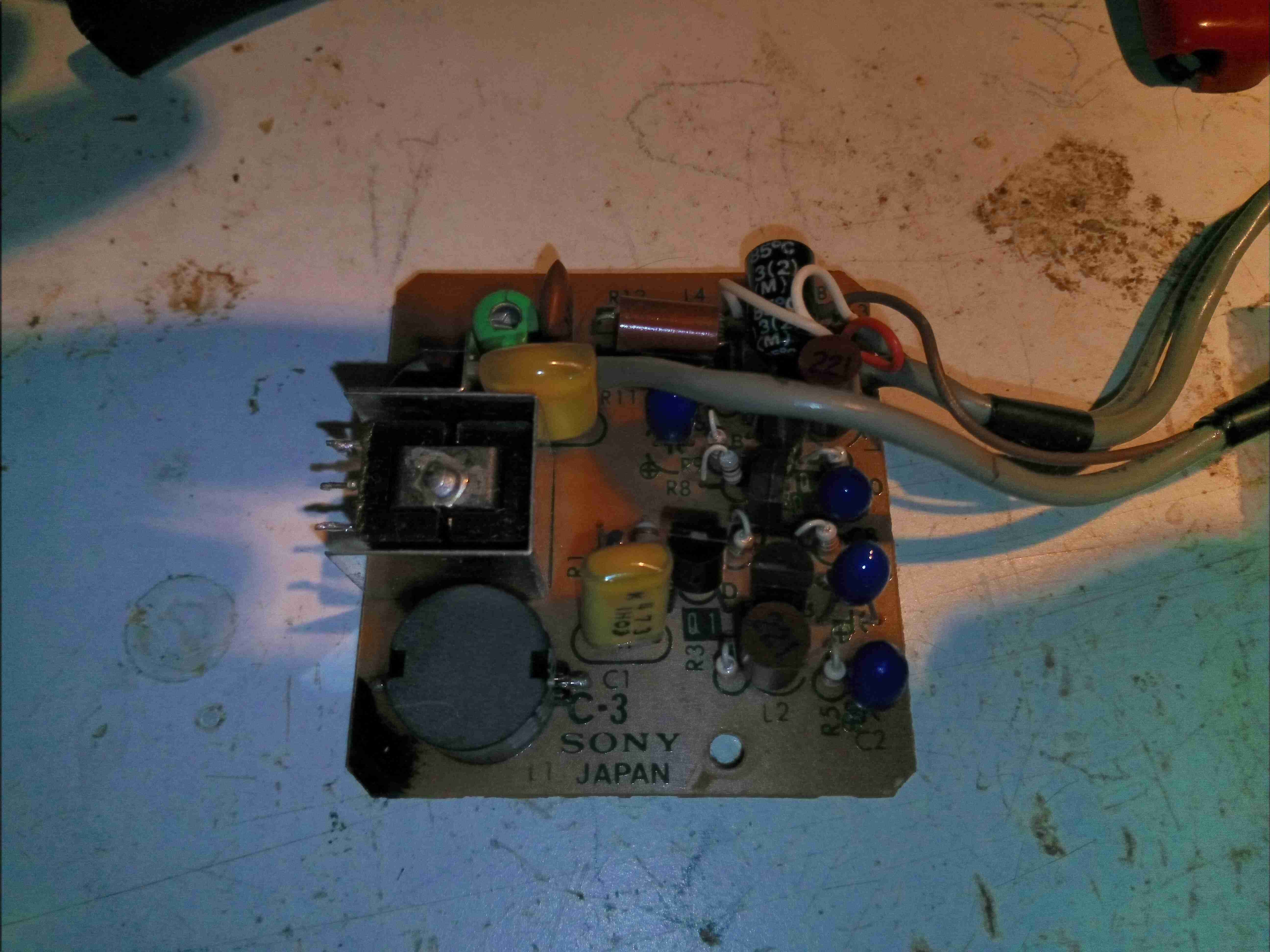
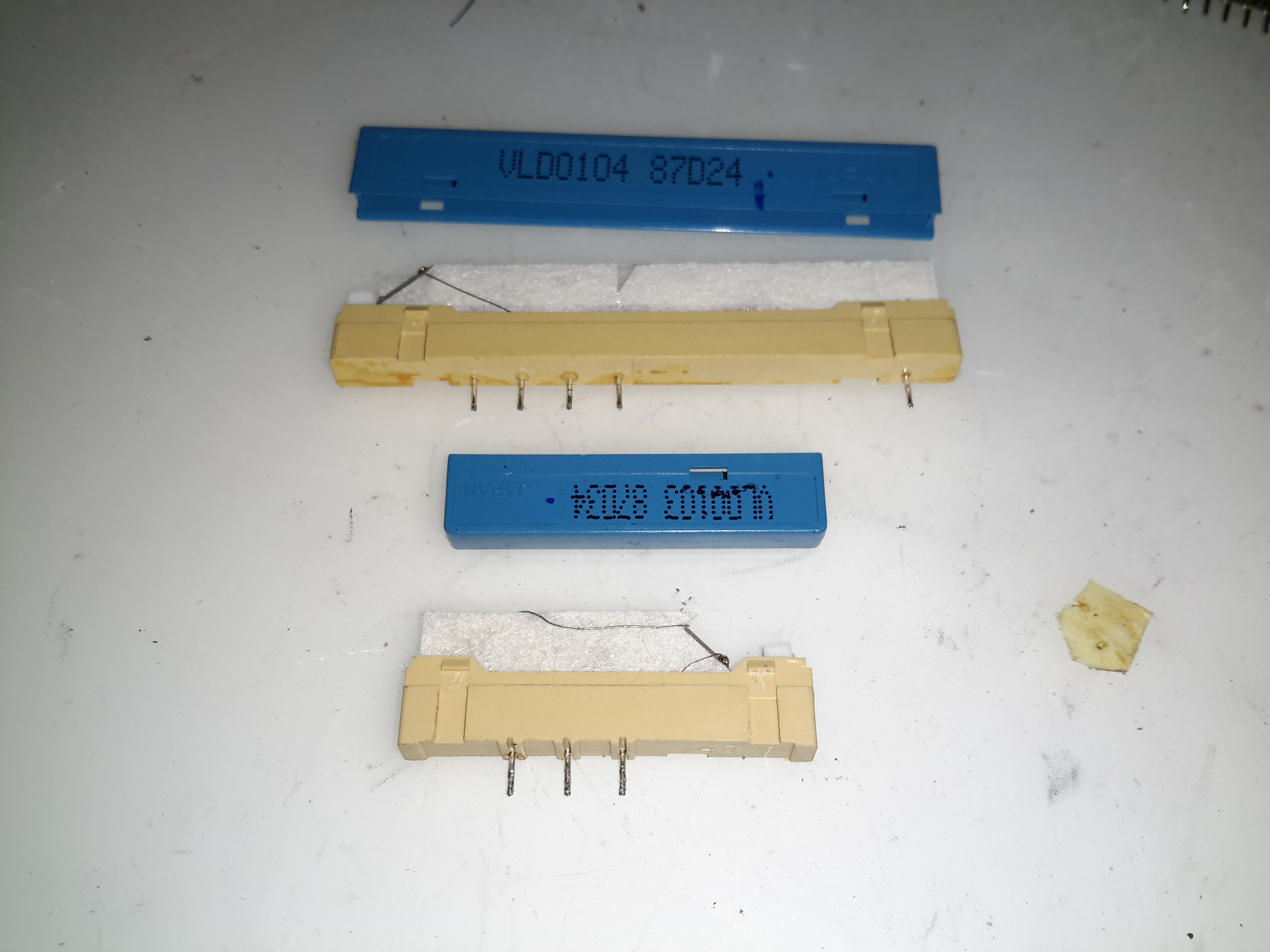
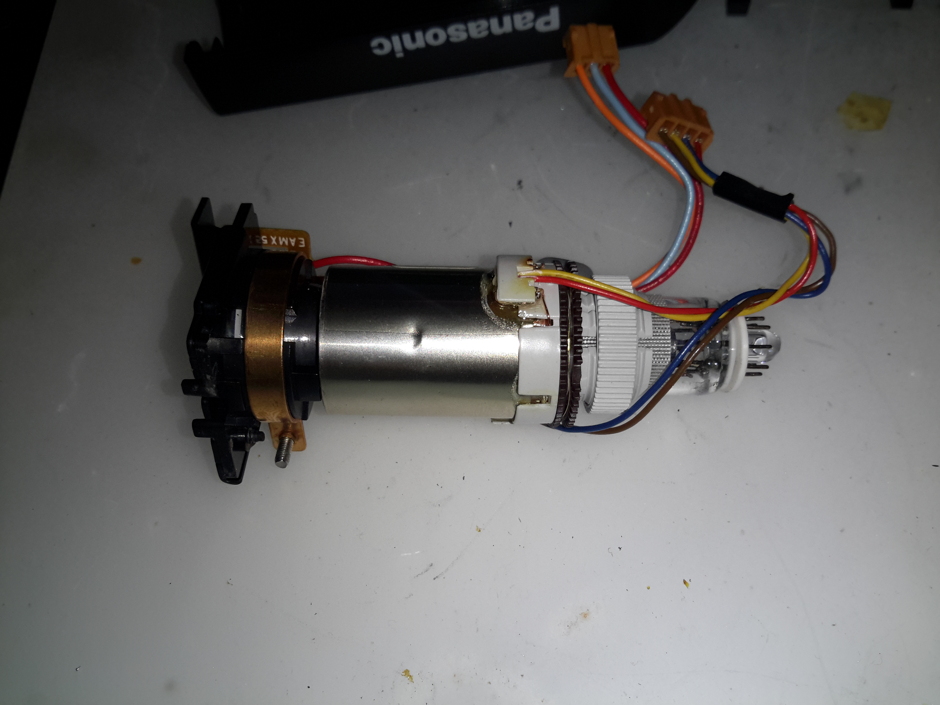
Removed from it’s shielding can, here is the head end amplifier for the Trinicon tube. This very sensitive JFET input amplifier feeds into the main video process board.

Input Transformer
Input Transformer

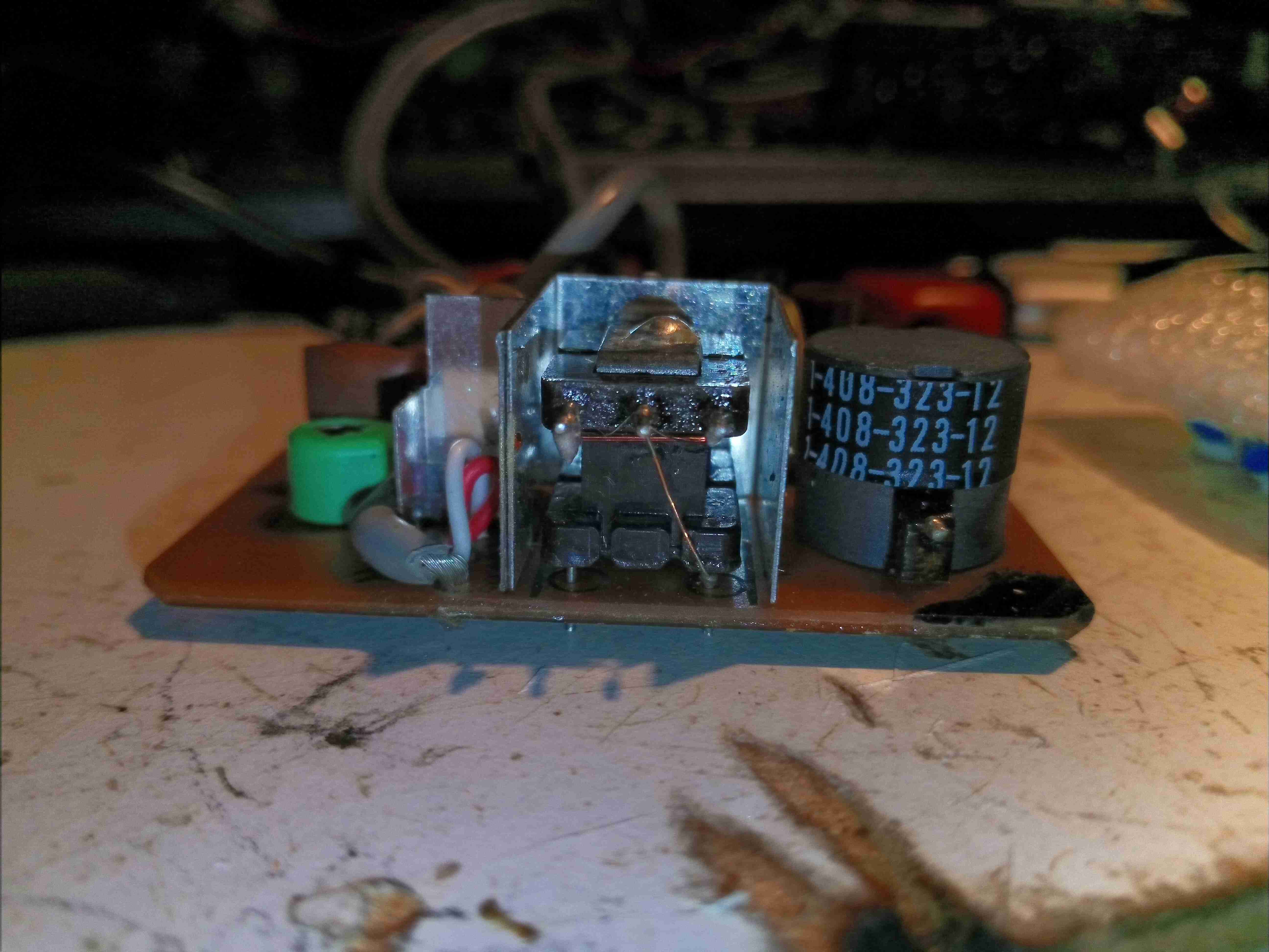
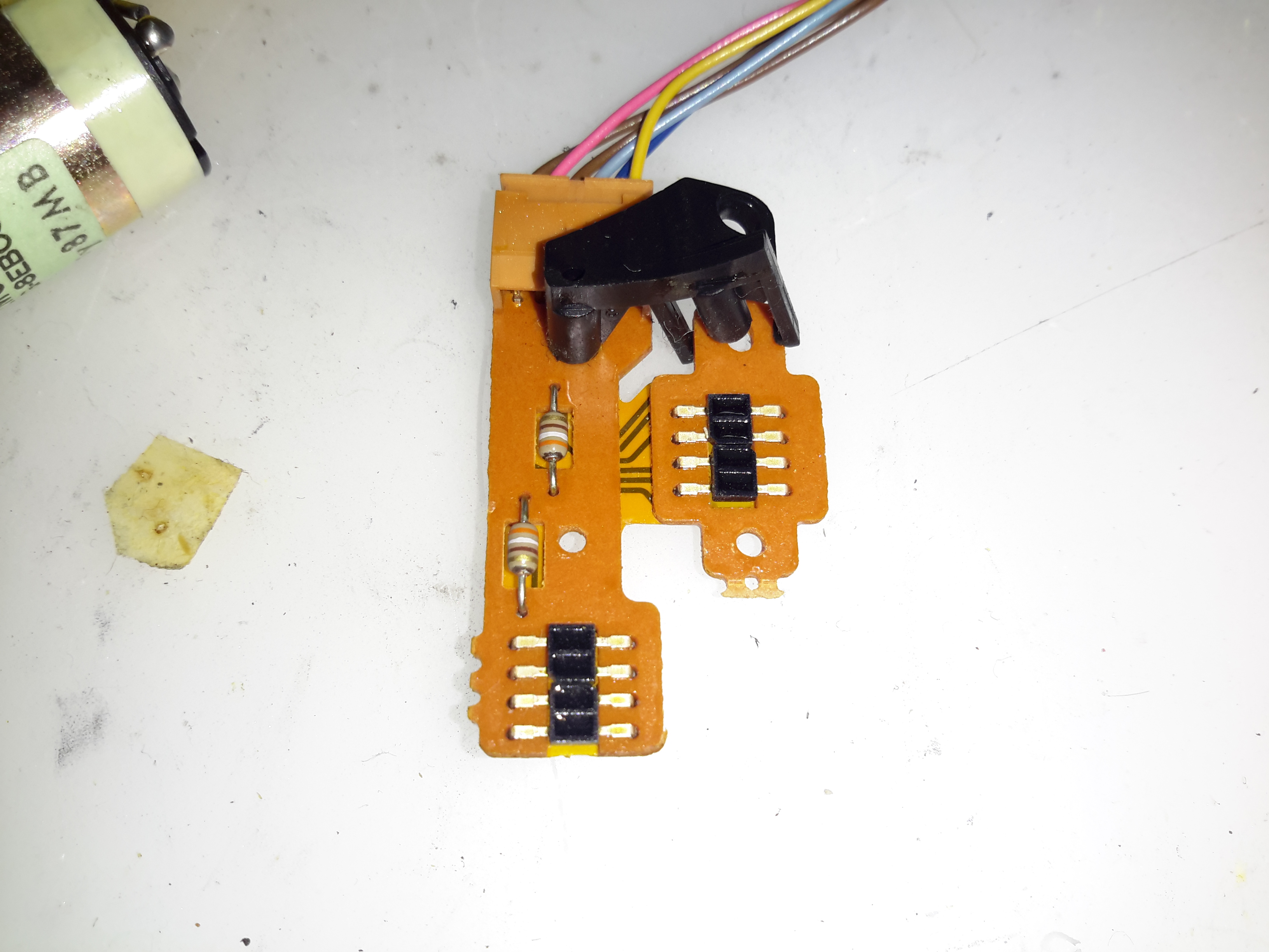
The Trinicon tube target connects to this input transformer on the front of the amplifier board.

Internal Video Adjustments

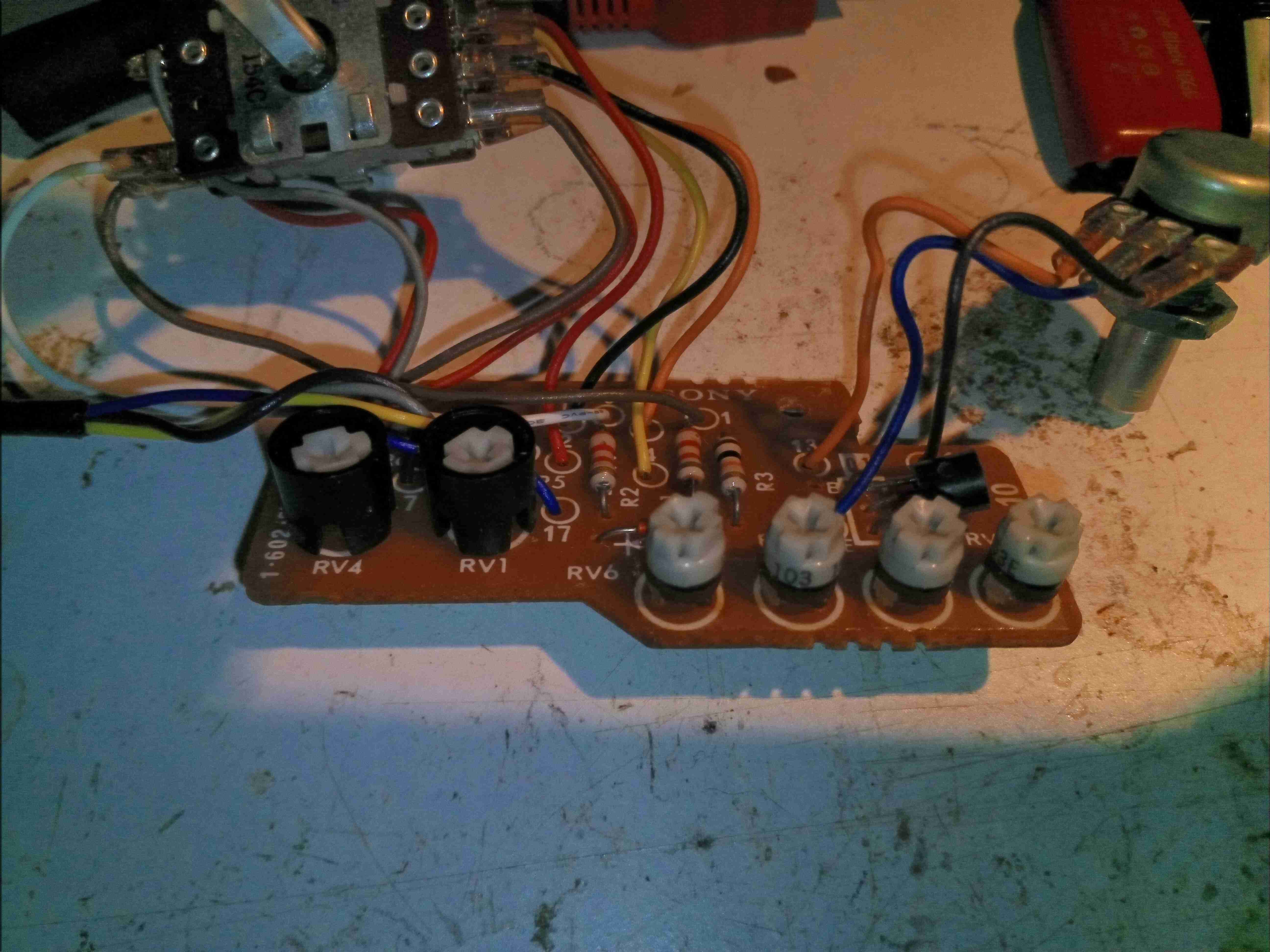
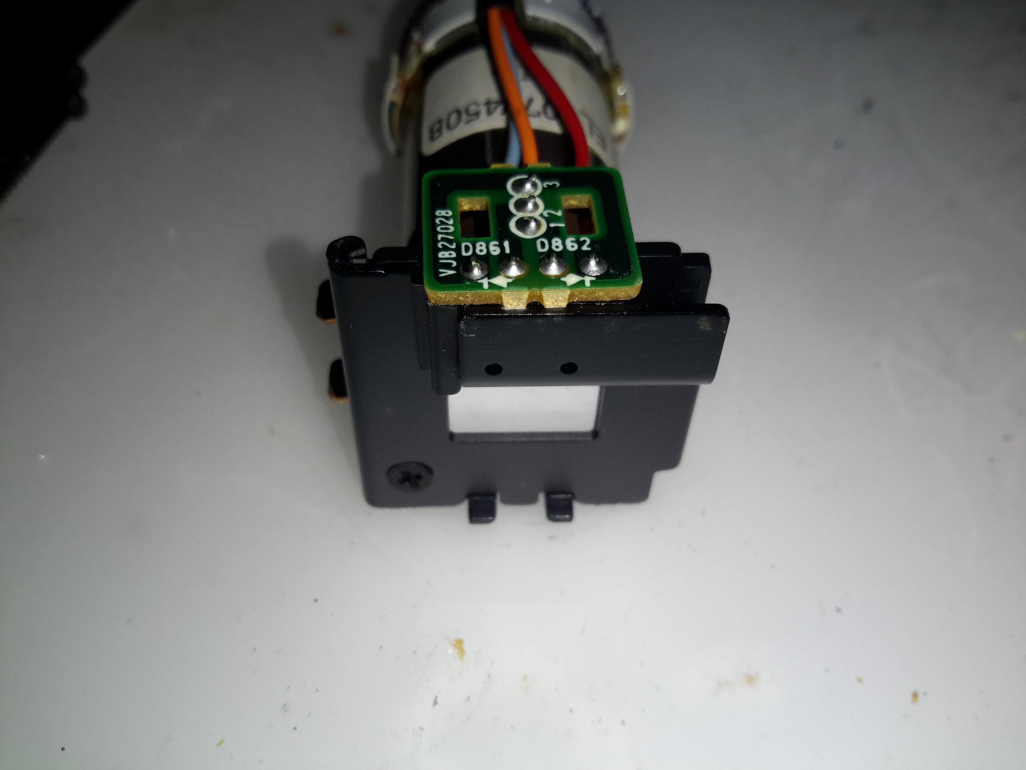
The internal white balance controls are on this small PCB, mounted under the user-accessible controls.

Vidicon Control Board

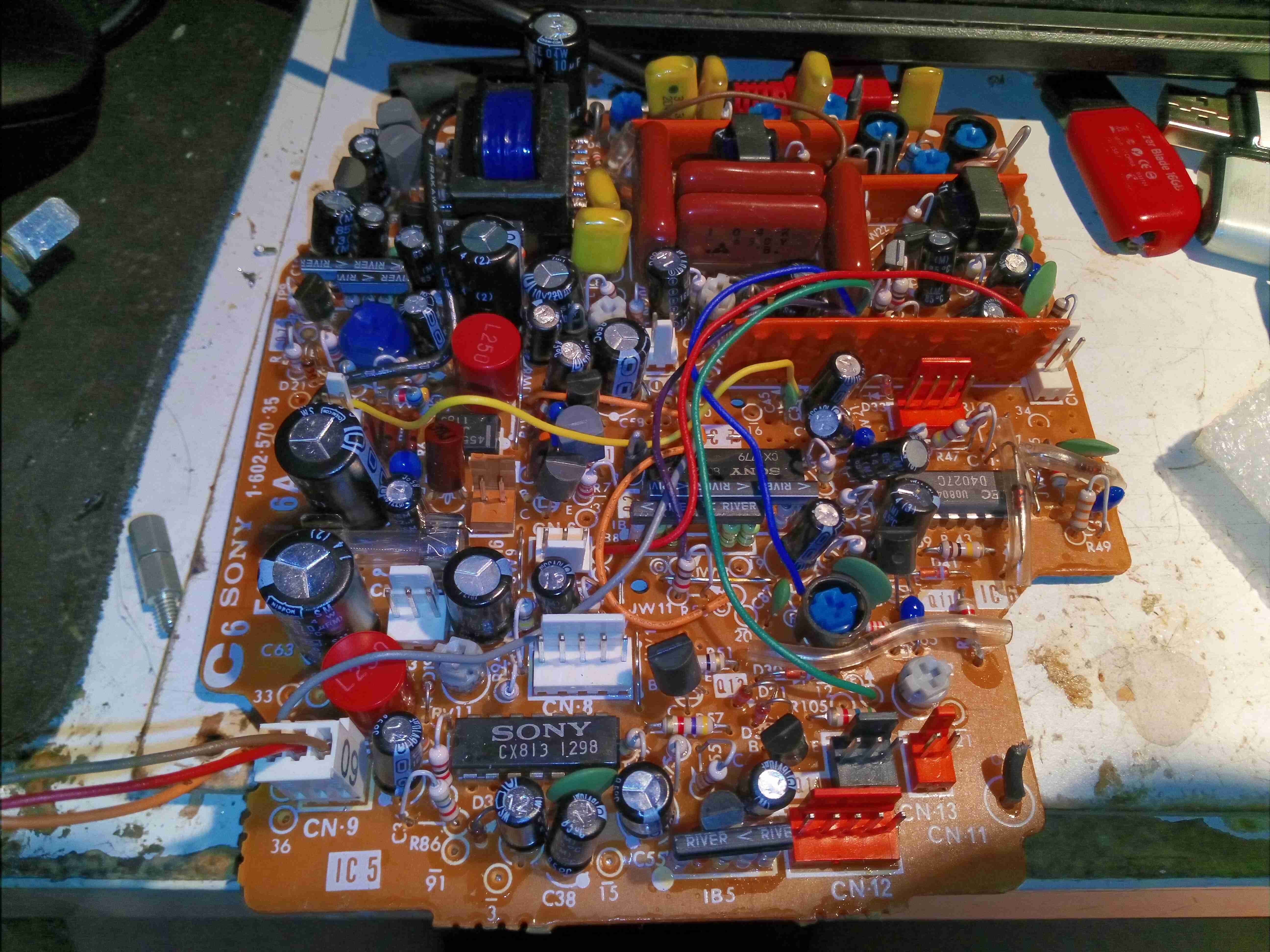
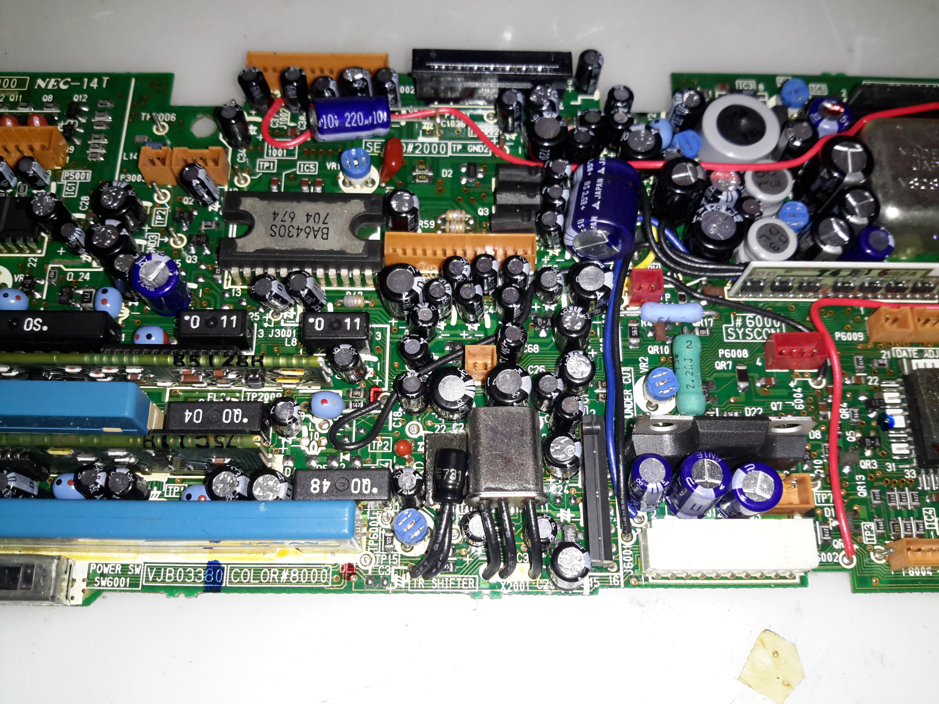
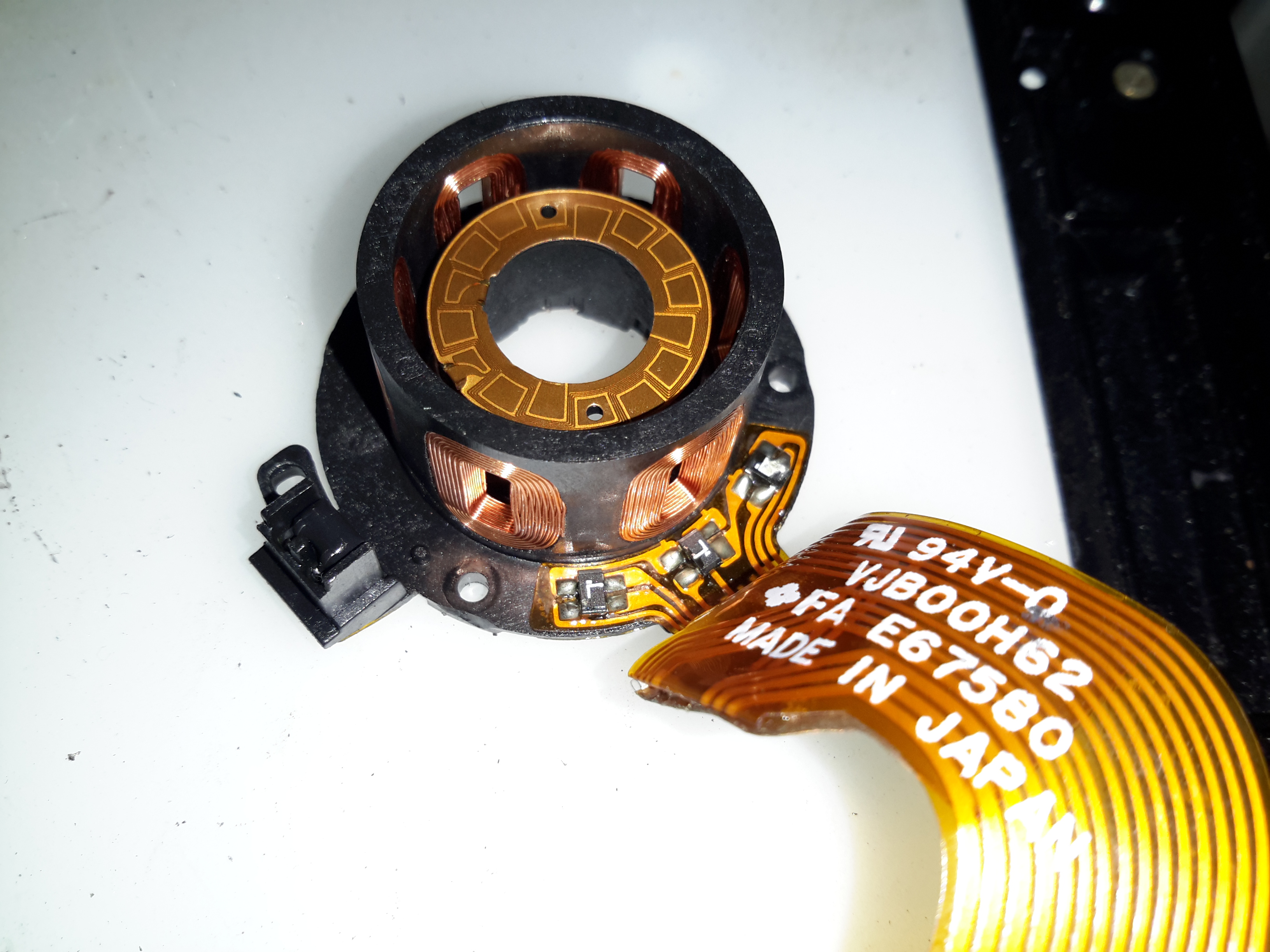
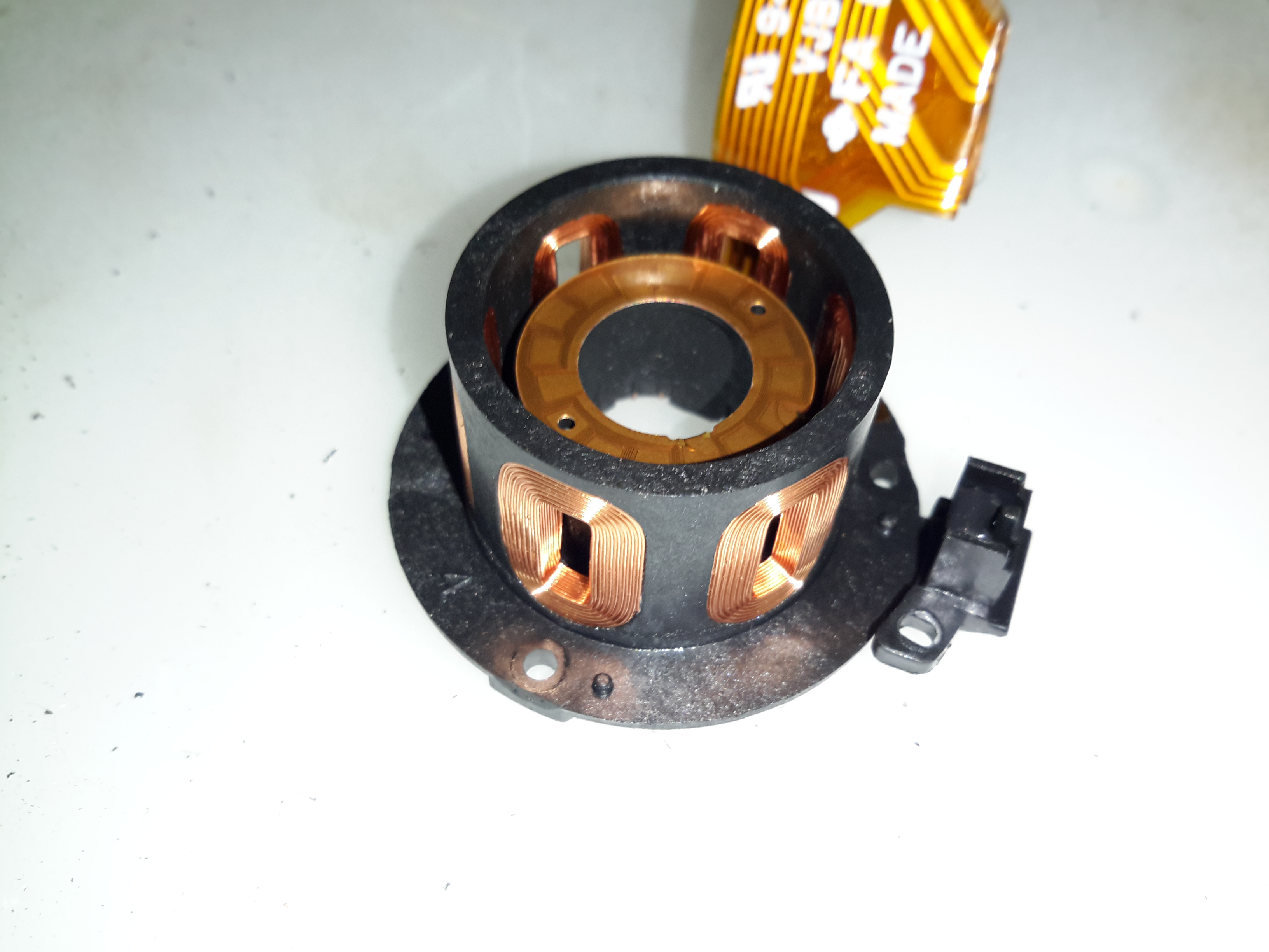
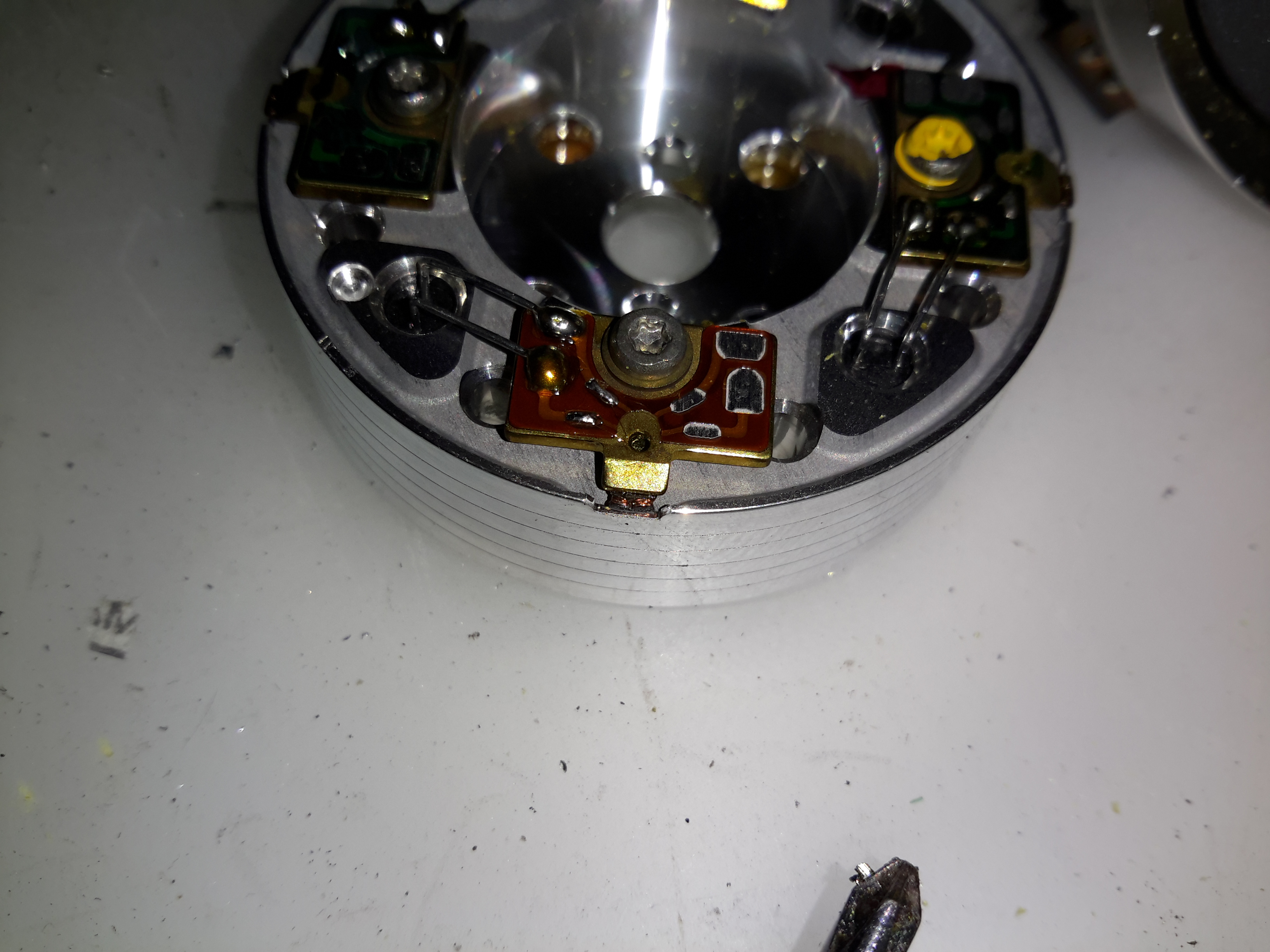
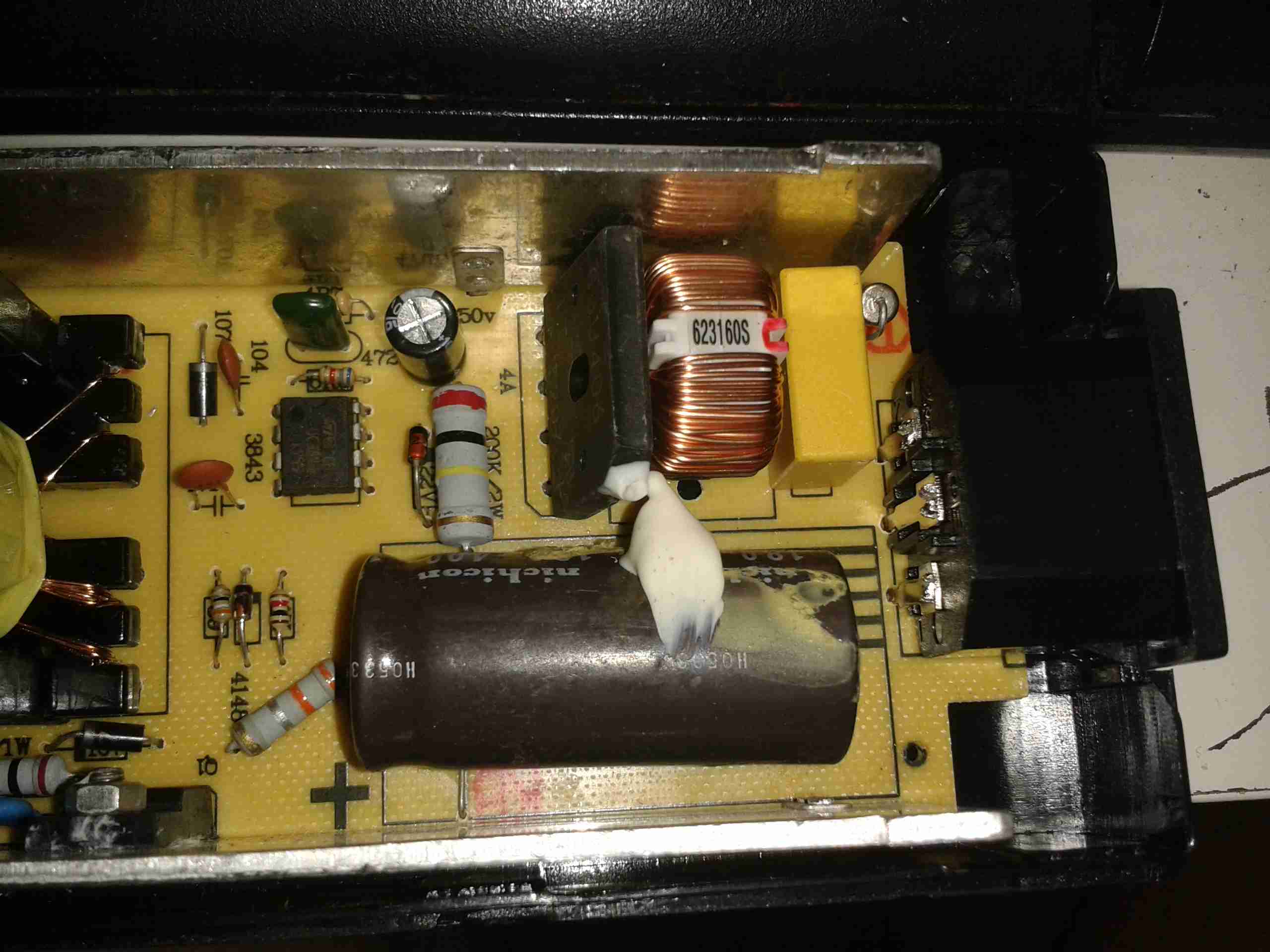
Here’s the main control board responsible for the Trinicon tube & exposure control. Down near the front is the auto-iris circuit, nearer the centre is timing control & at the top is the high voltage power supply & deflection generator ICs.

High Voltage Section

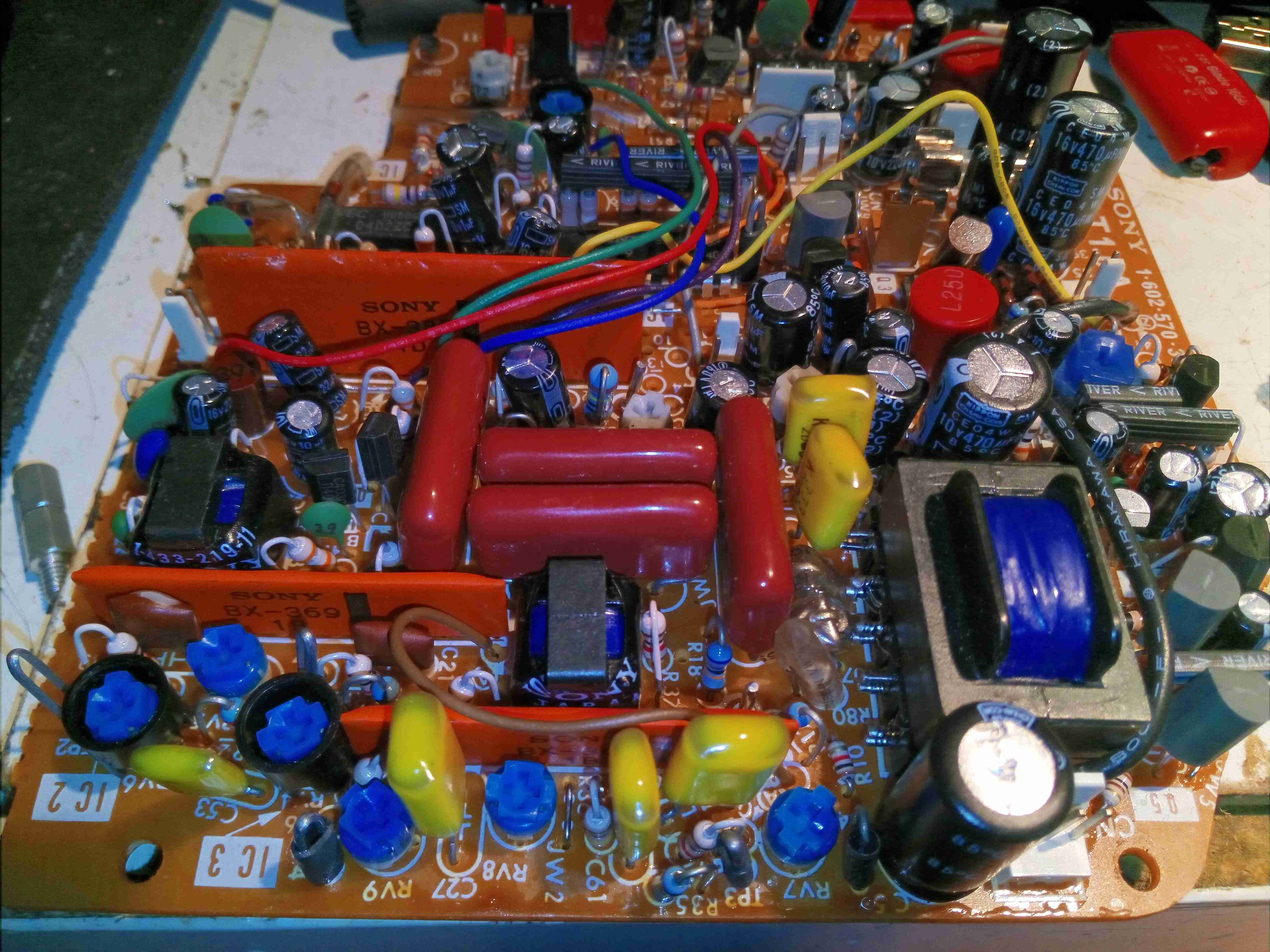
Here’s the high voltage section, the main transformer at right generating the voltages required to drive the video tube. The large orange hybrids here are a pair of BX369 high-voltage sawtooth generators that create the deflection waveforms for the tube. The other large hybrid is a BX382 Fader Control.

Video Process Board
Video Process Board

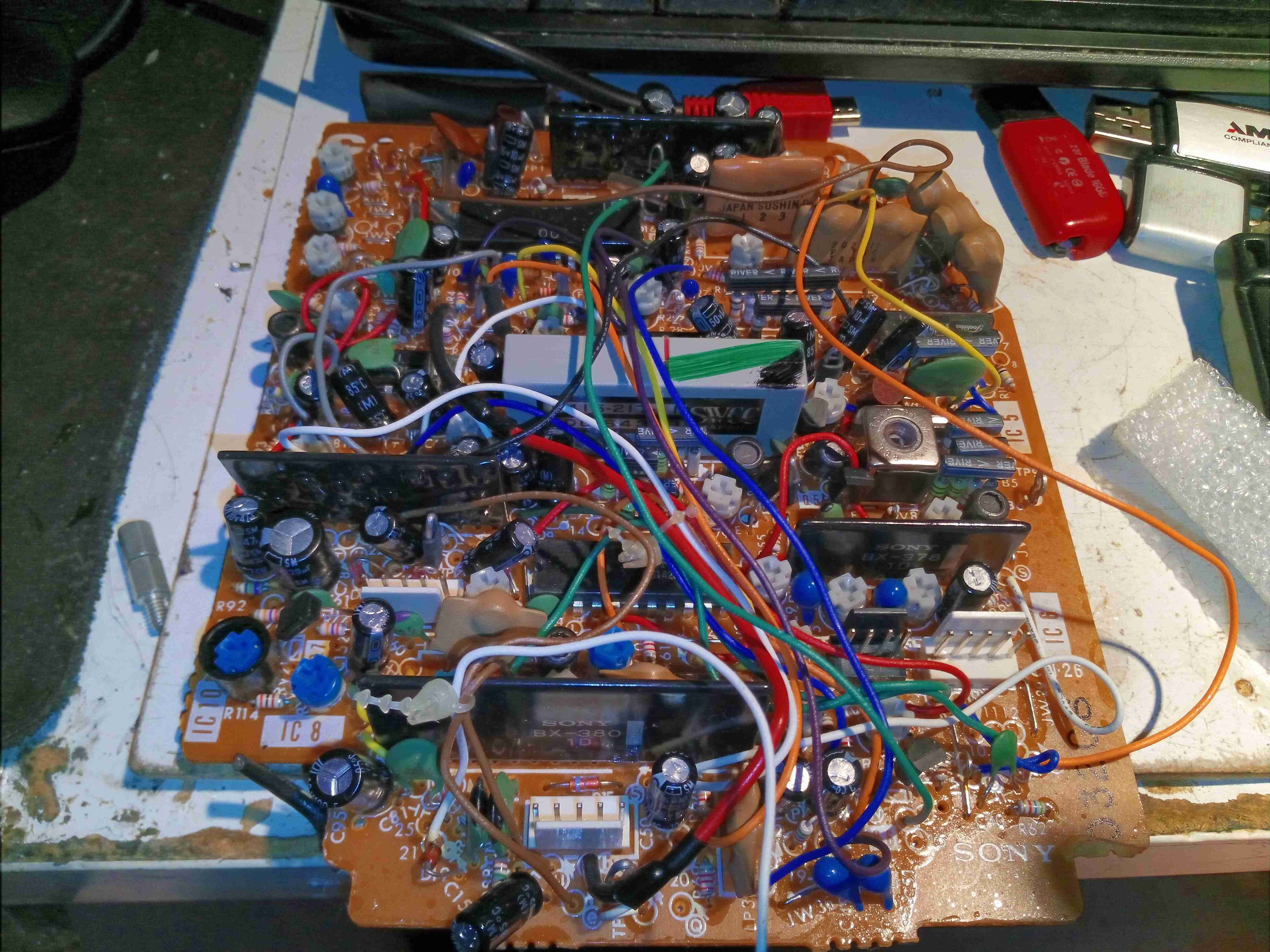
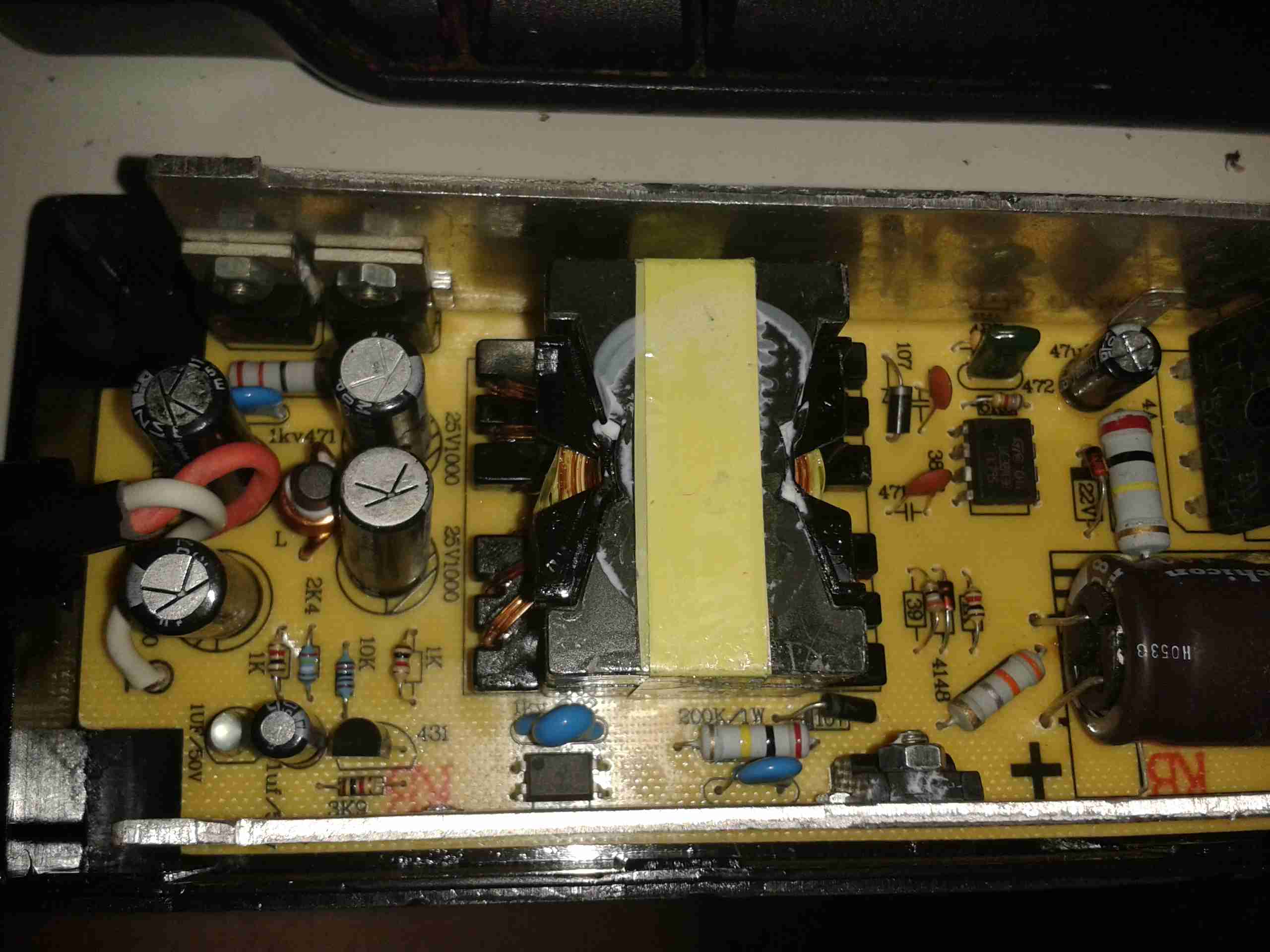
The other large board contains all the video process circuitry, all analogue of course. There are a lot of manual adjustment pots on this board.

Lens Barrel
Lens Barrel

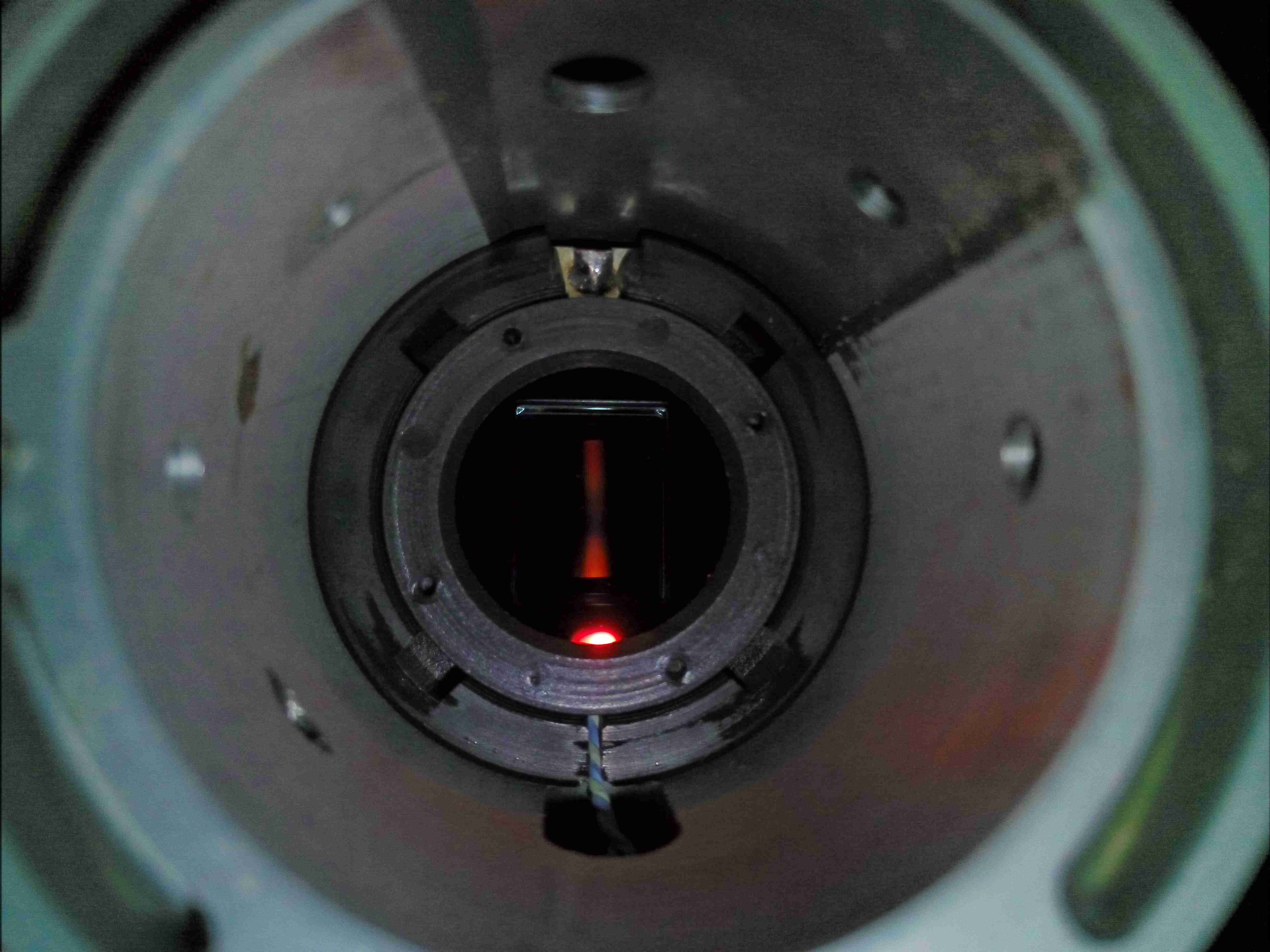
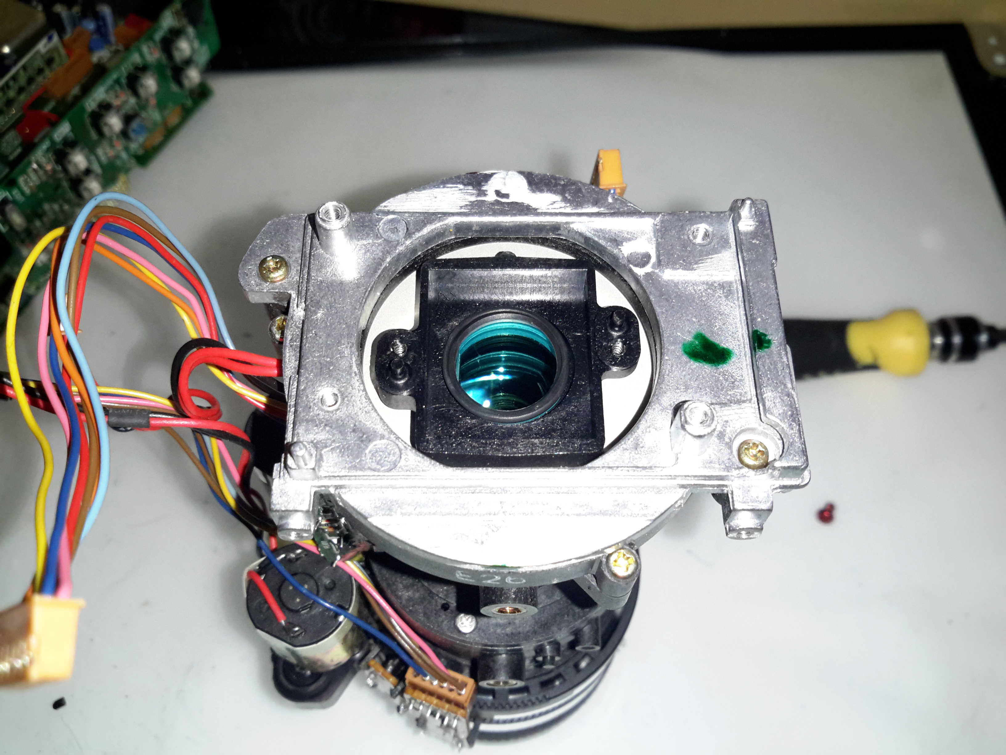
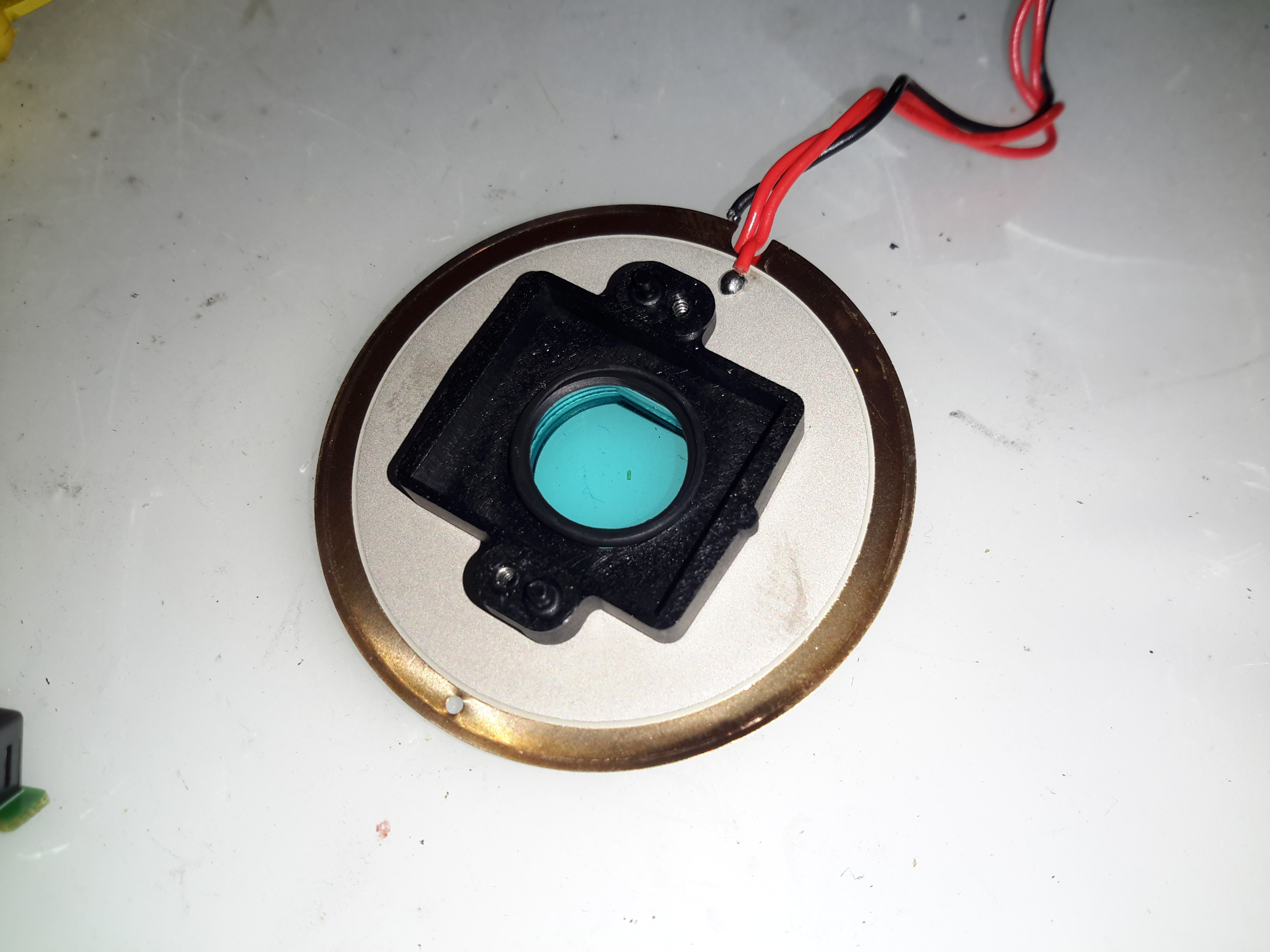
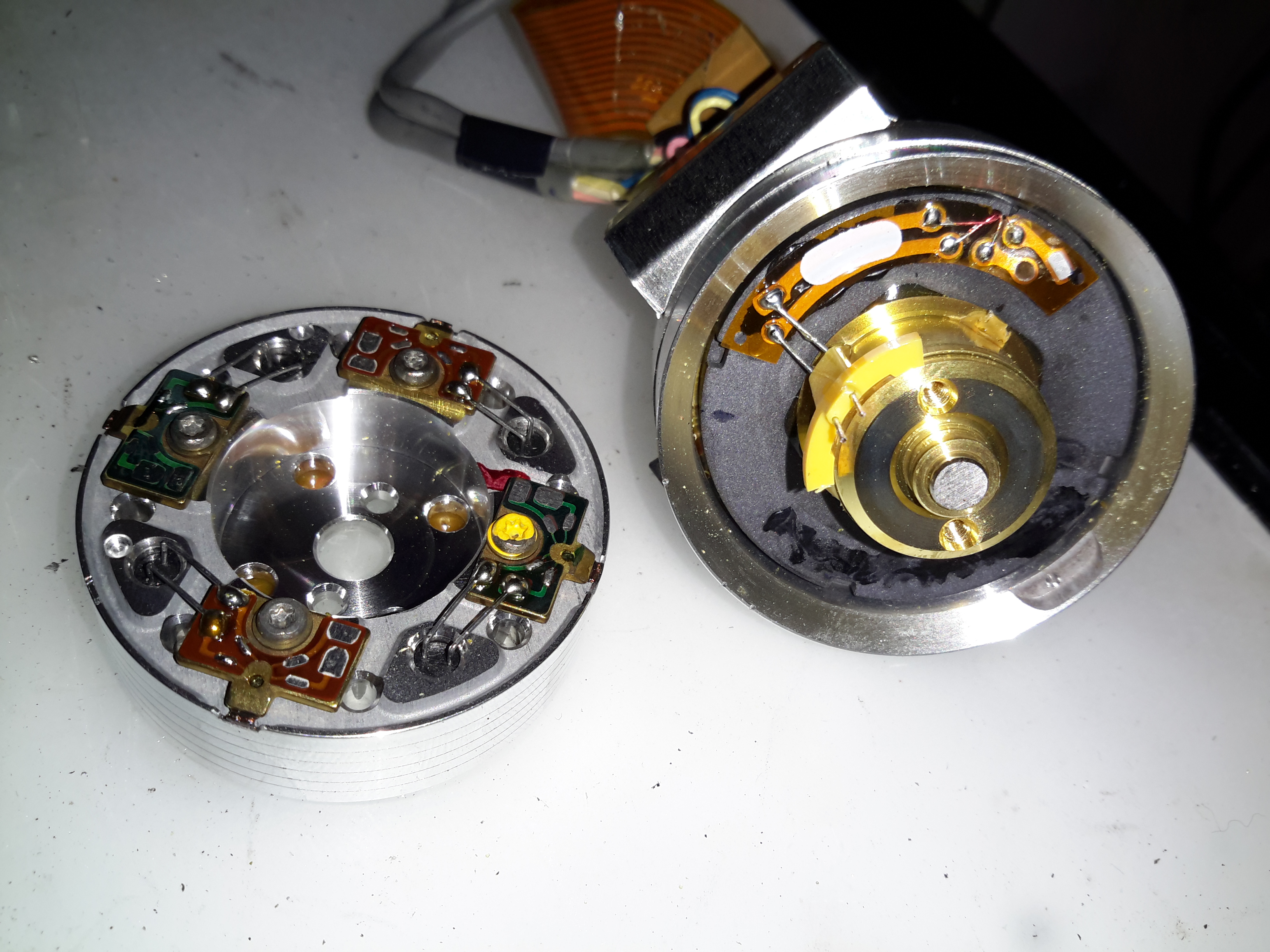
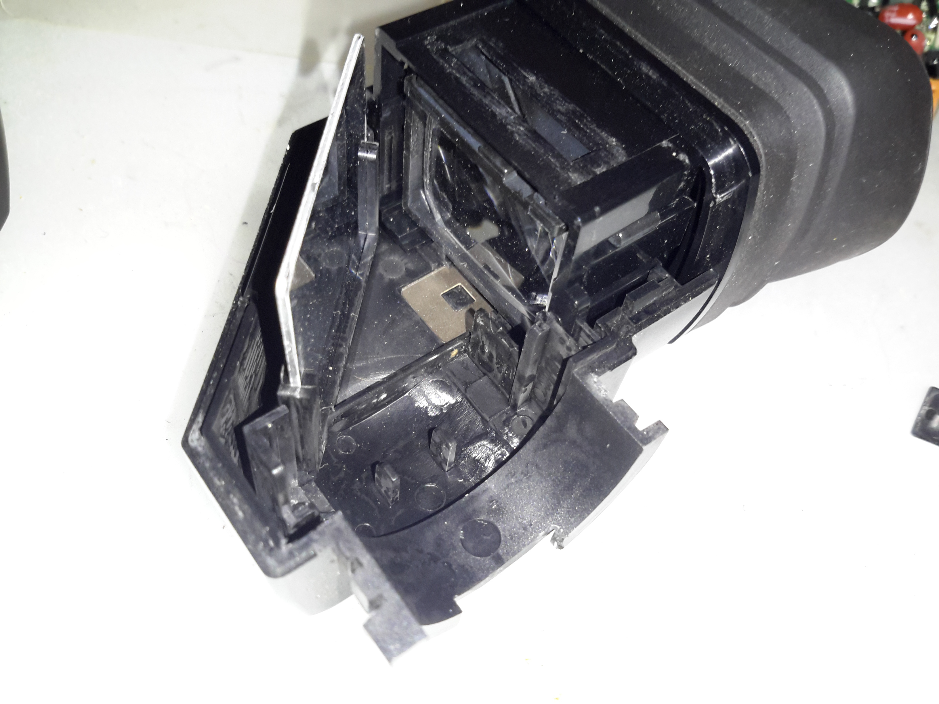
After removing the lens assembly, the tube assembly is visible inside the barrel casting. Not much to see yet, just the IR filter assembly.

Trinicon Tube Assembly

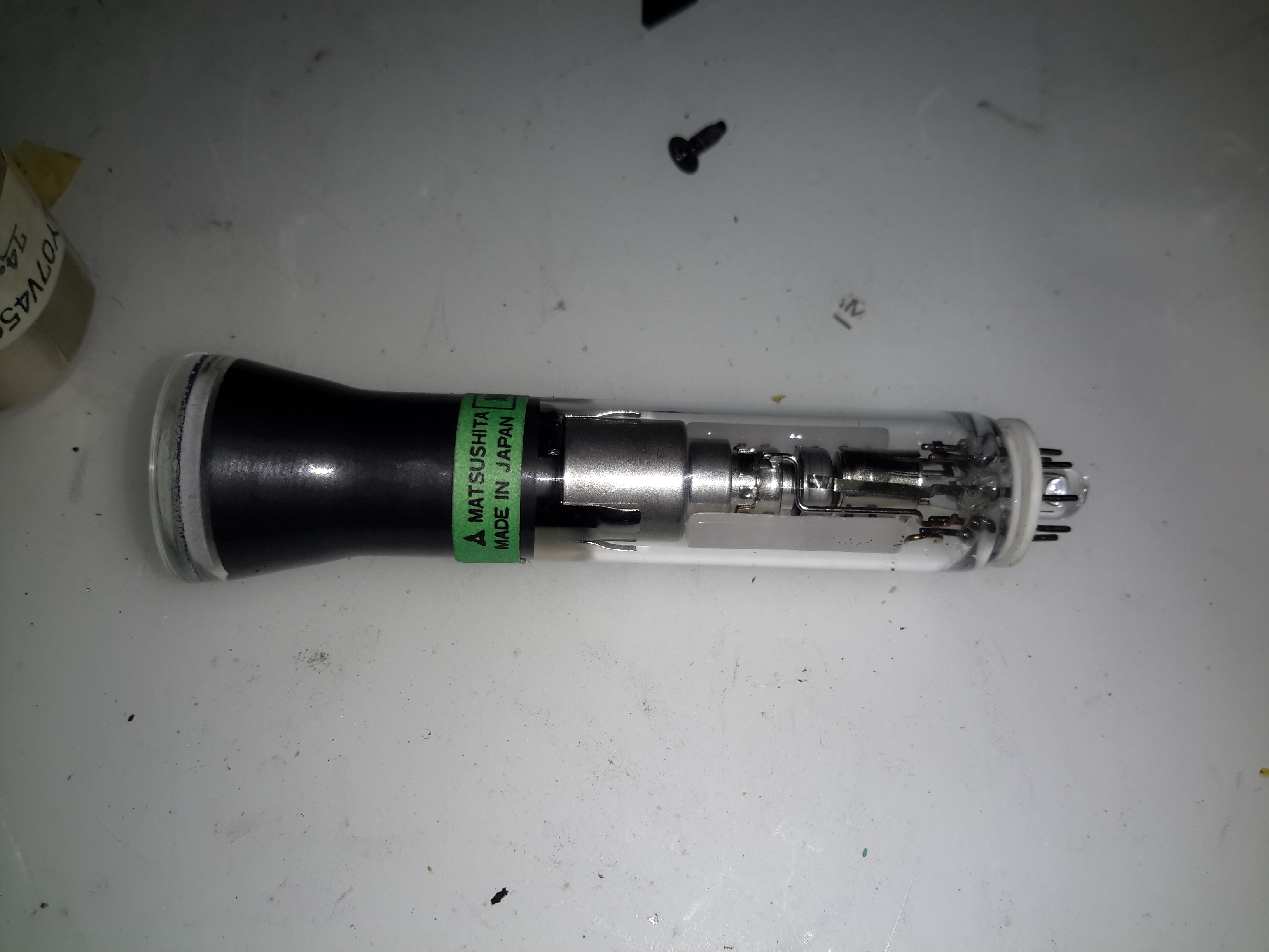
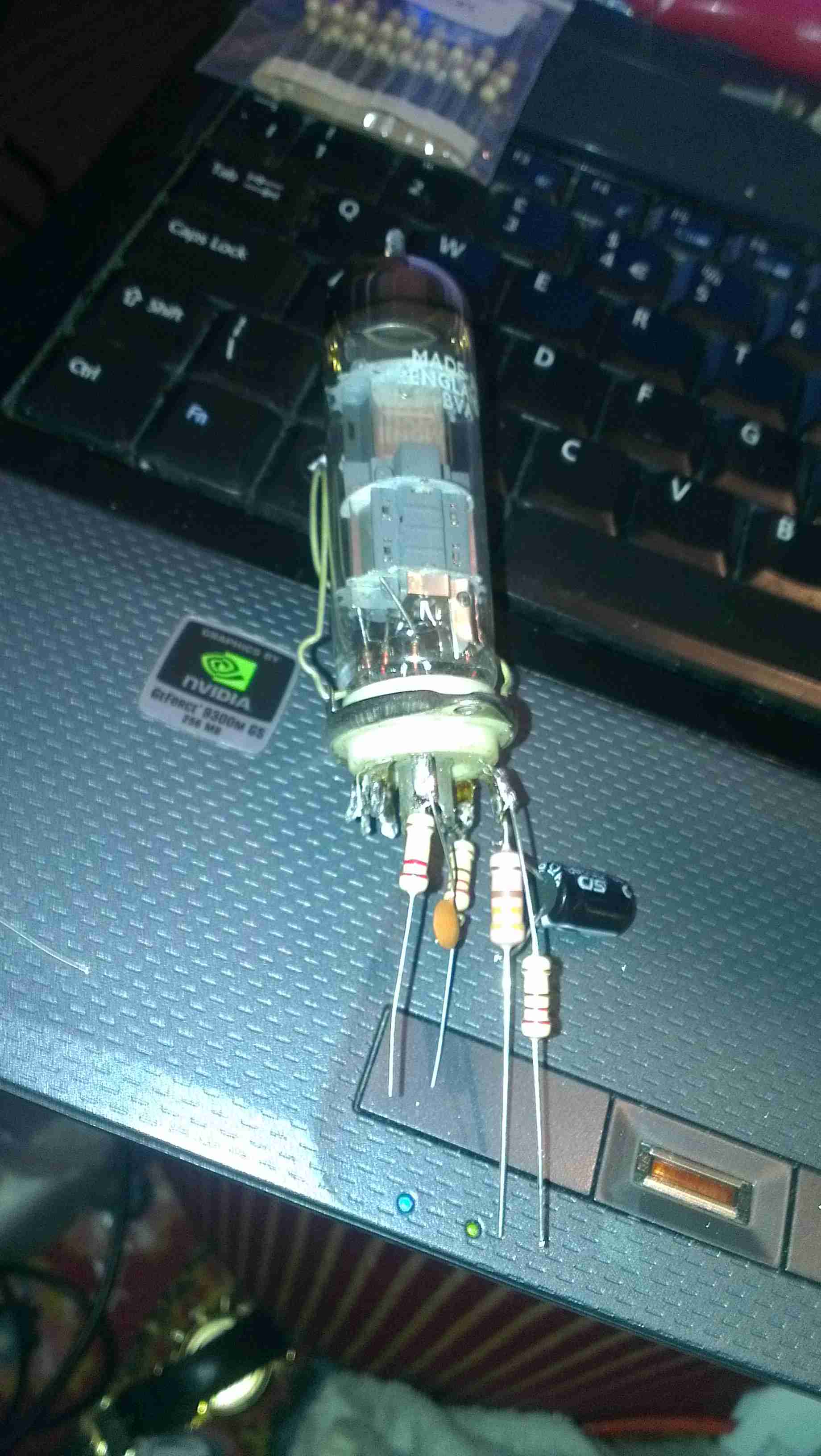
Here’s the unit removed from the camera. Unfortunately this tube is dead – it shows a lot of target burn on the resulting image, and very bad ghosting on what poor image there is. The Trinicon tube itself is encased in the focus coil assembly, the windings of which are hidden under the shielding.

IR Filter
IR Filter

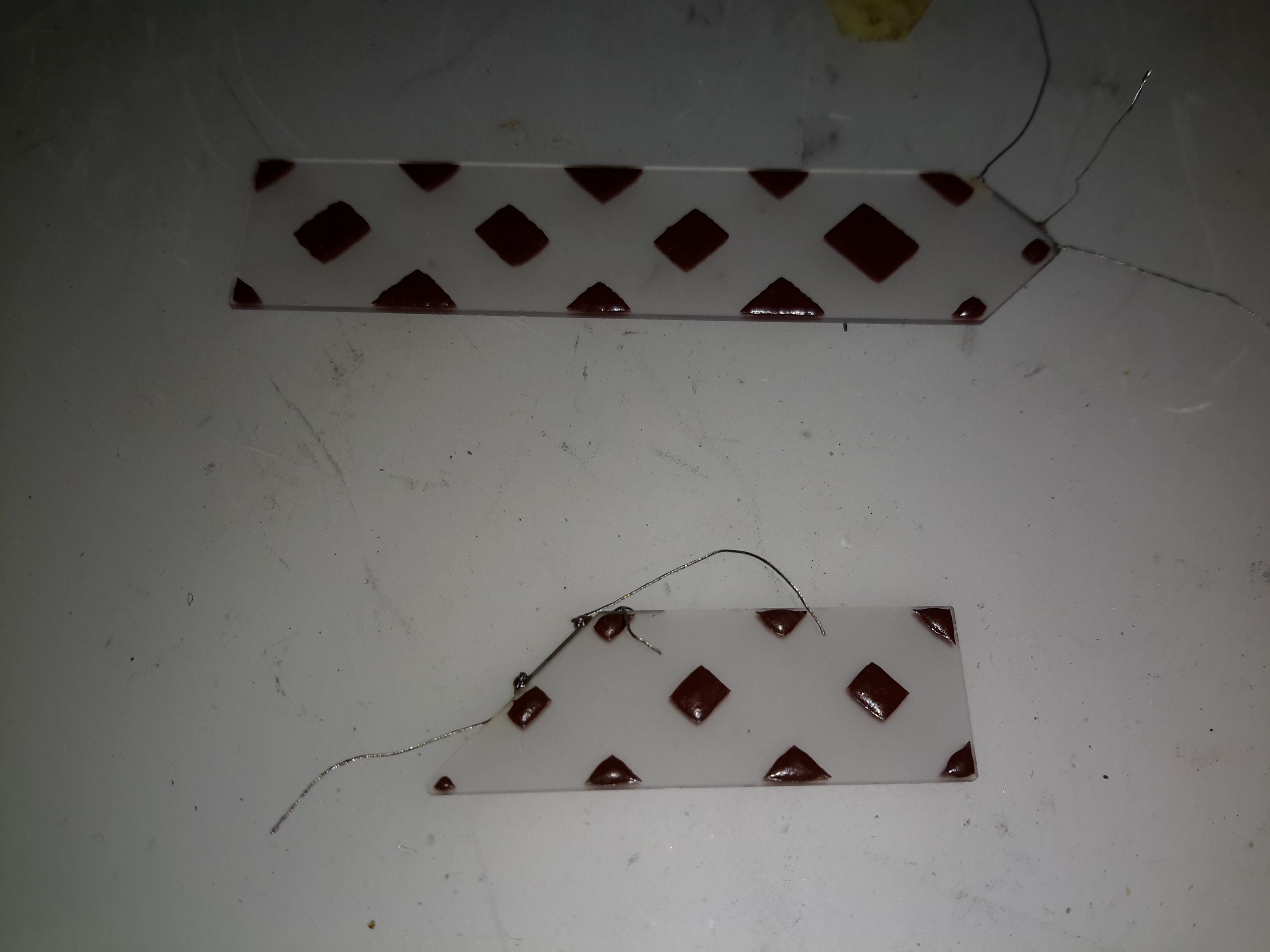
The IR filter is locked into the front of the tube, on a bayonet fitting. The twin target wires are running off to the left, where they would connect to the head end amplifier.

Bare Tube
Bare Tube

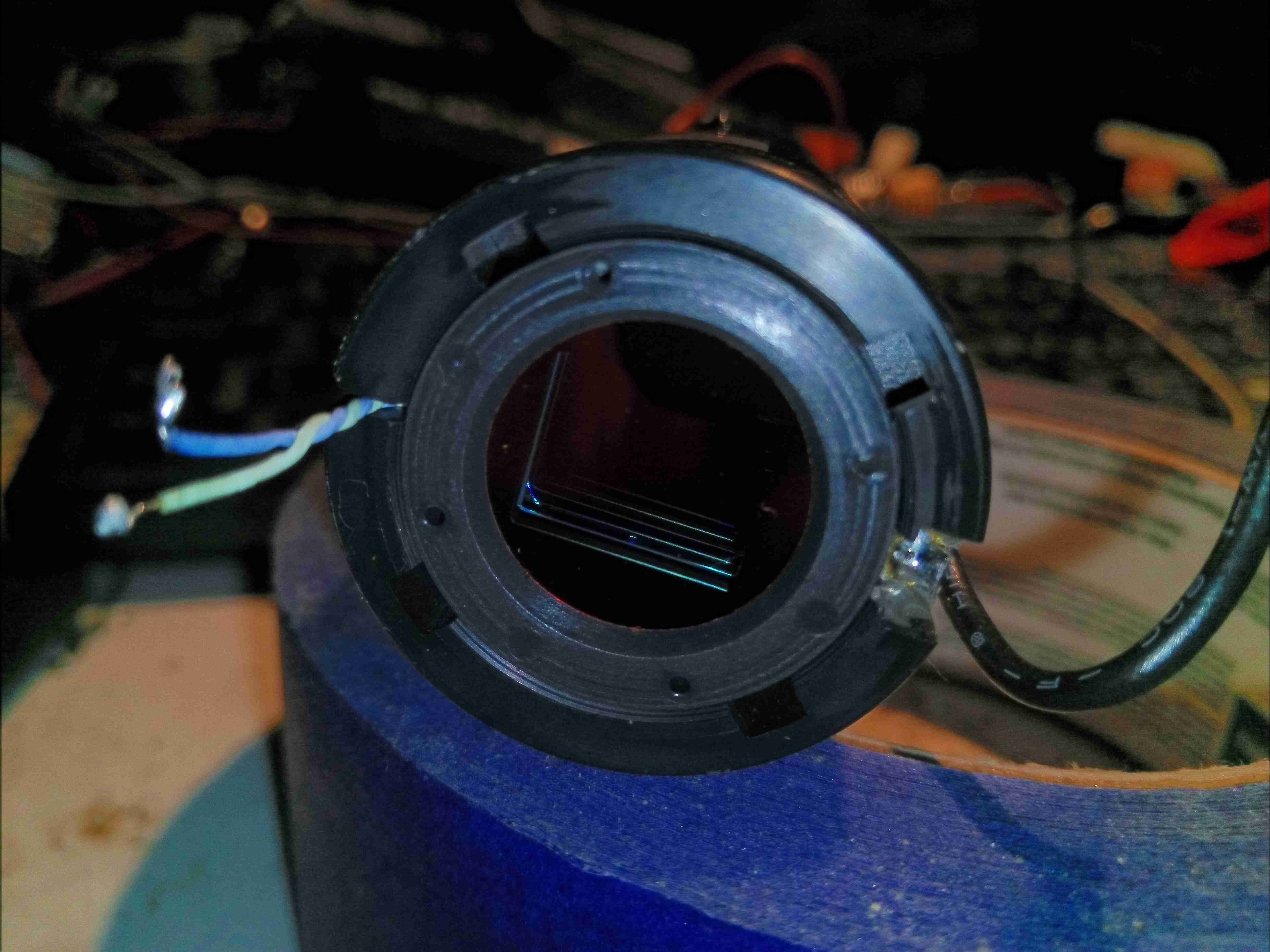
After removing the IR filter glass, the Trinicon tube itself is removed from the focus coil assembly. There’s an electron gun at the rear of the tube, like all CRTs, although this one works in reverse – sensing an image projected on the front instead of generating one.

Deflection Plates
Deflection Plates

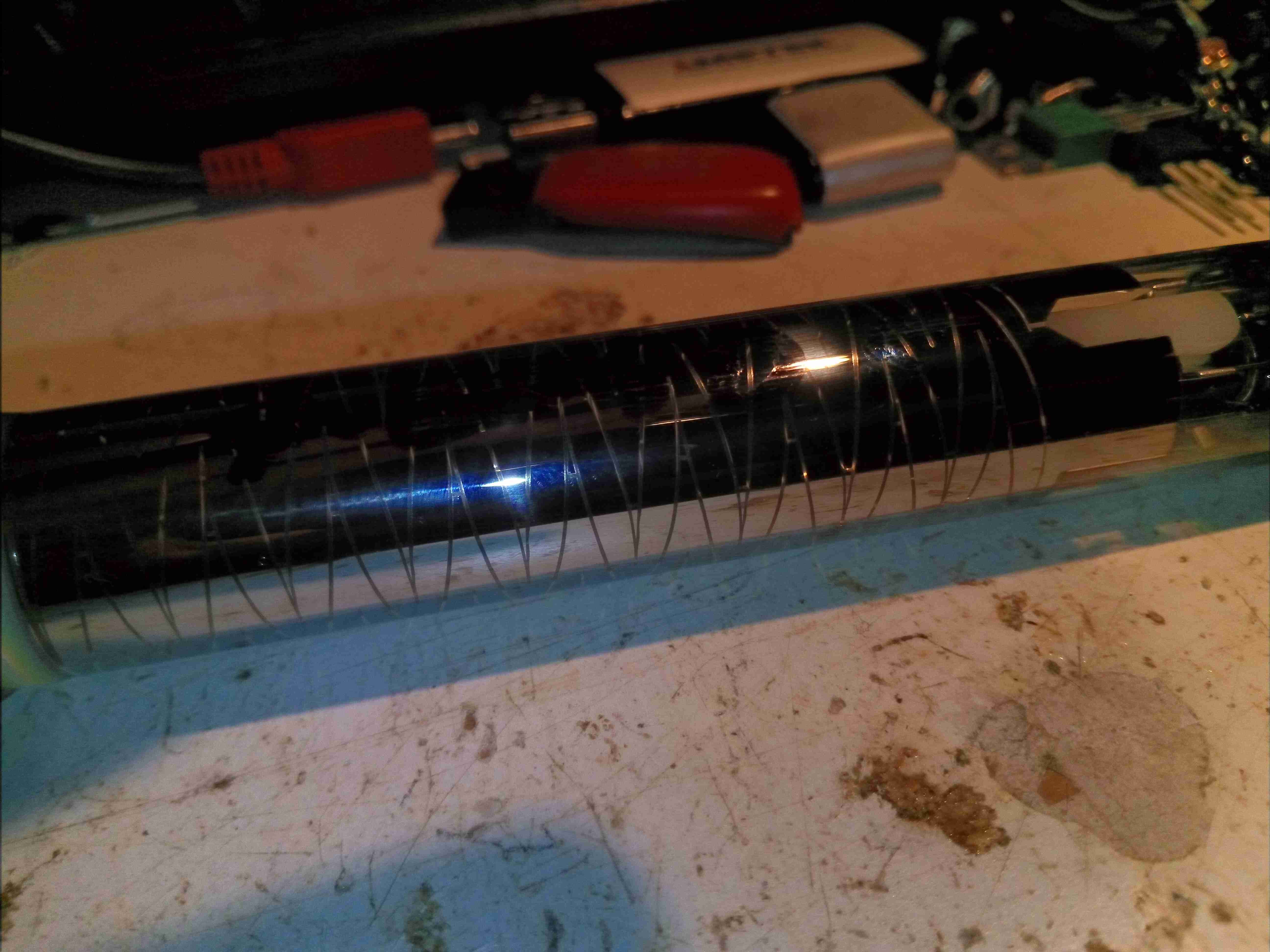
It’s a little difficult to see, but the electrostatic deflection electrodes in this tube are created from the aluminium flashing on the inside of the glass, in a zig-zag pattern. The interleaving electrodes are connected to base pins by spring contacts at the electron gun end of the tube.

Electron Gun
Electron Gun

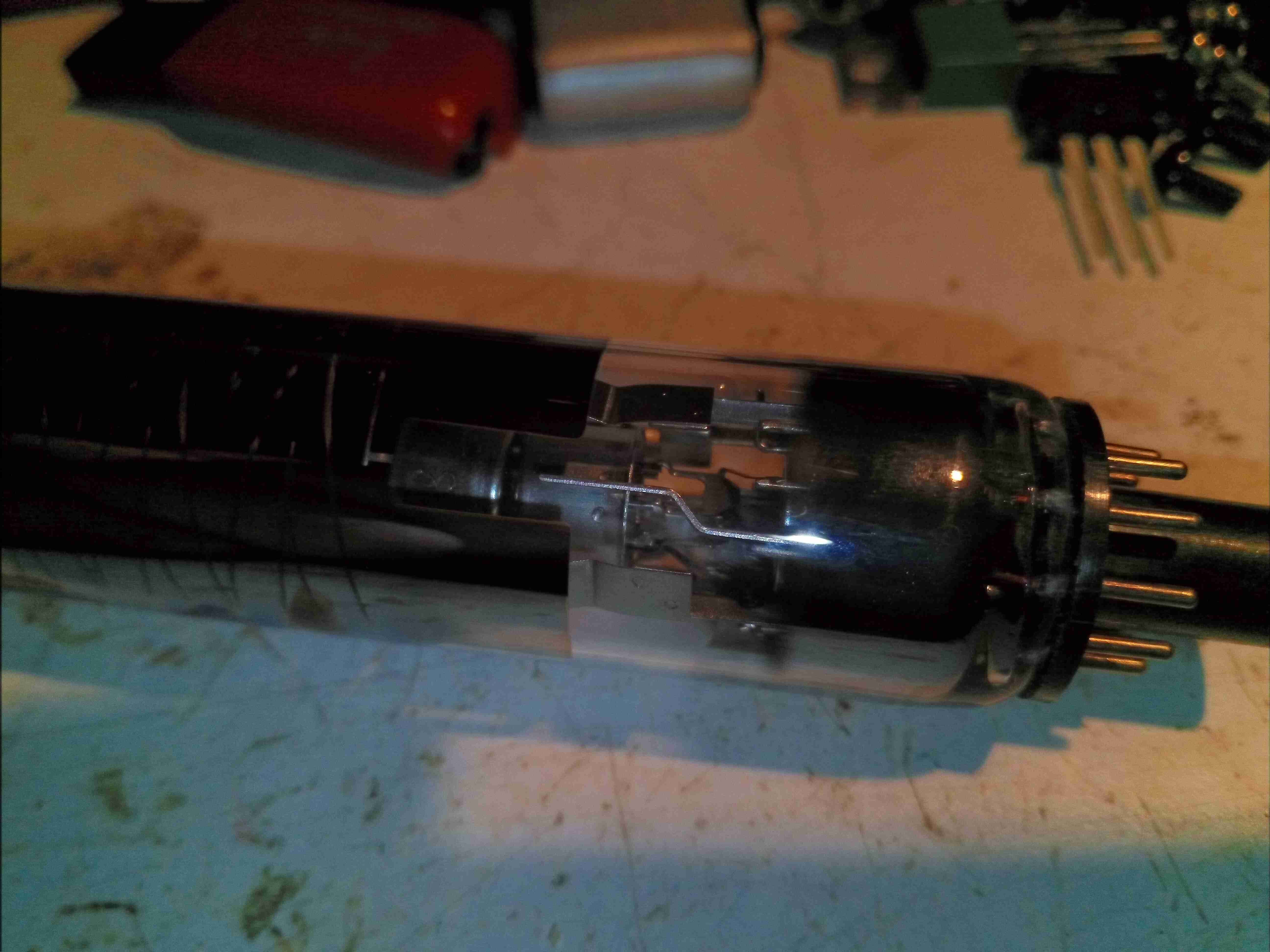
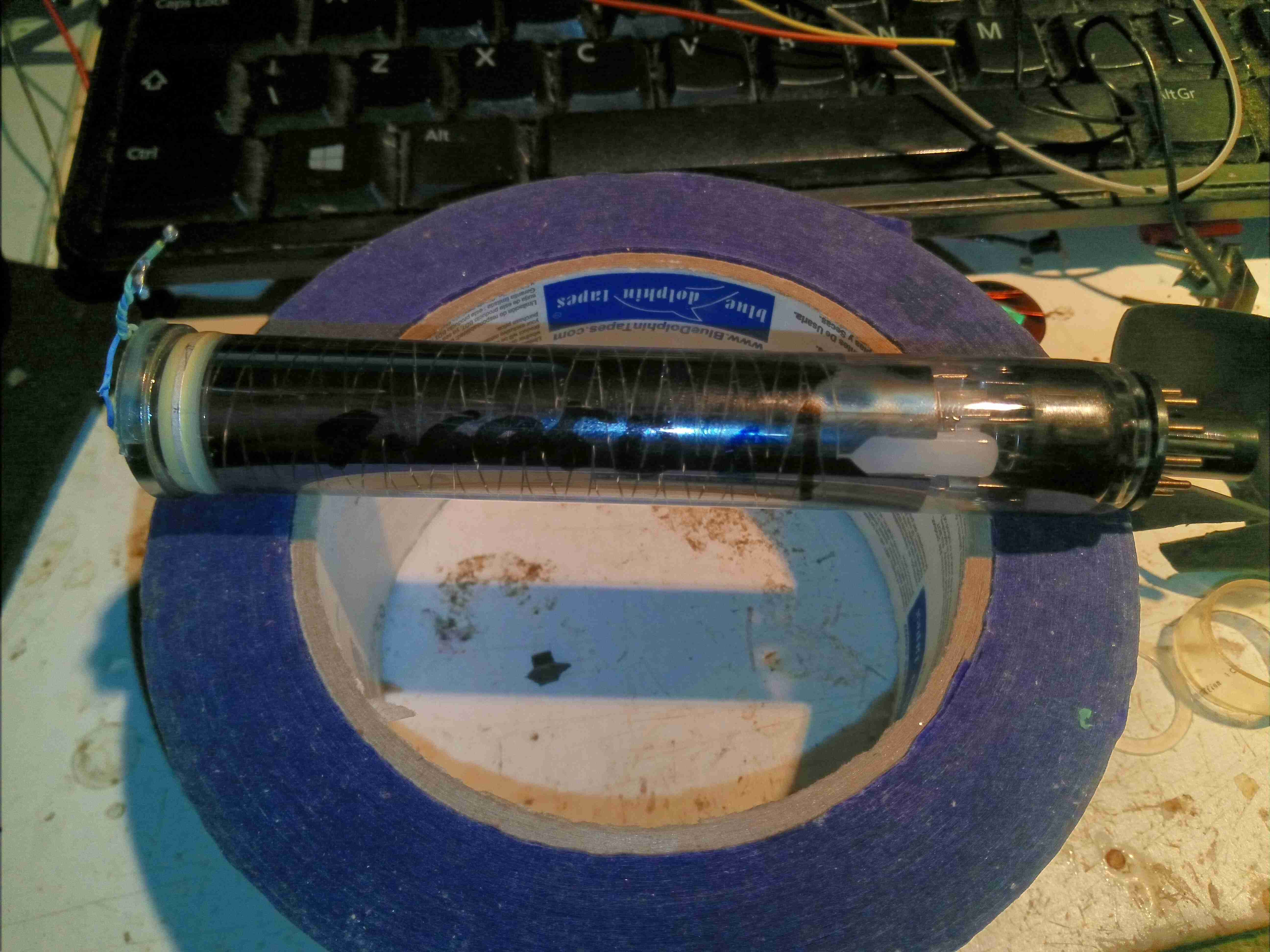
The electron gun is mostly hidden by the getter flash & the deflection electrodes, but the cathode can is visible through the glass, along with the spring contacts that make a connection to the deflection electrodes. This is also a very short gun – it doesn’t extend more than about 5mm into the deflection zone. The rest of the tube up to the target is empty space.

Target
Target

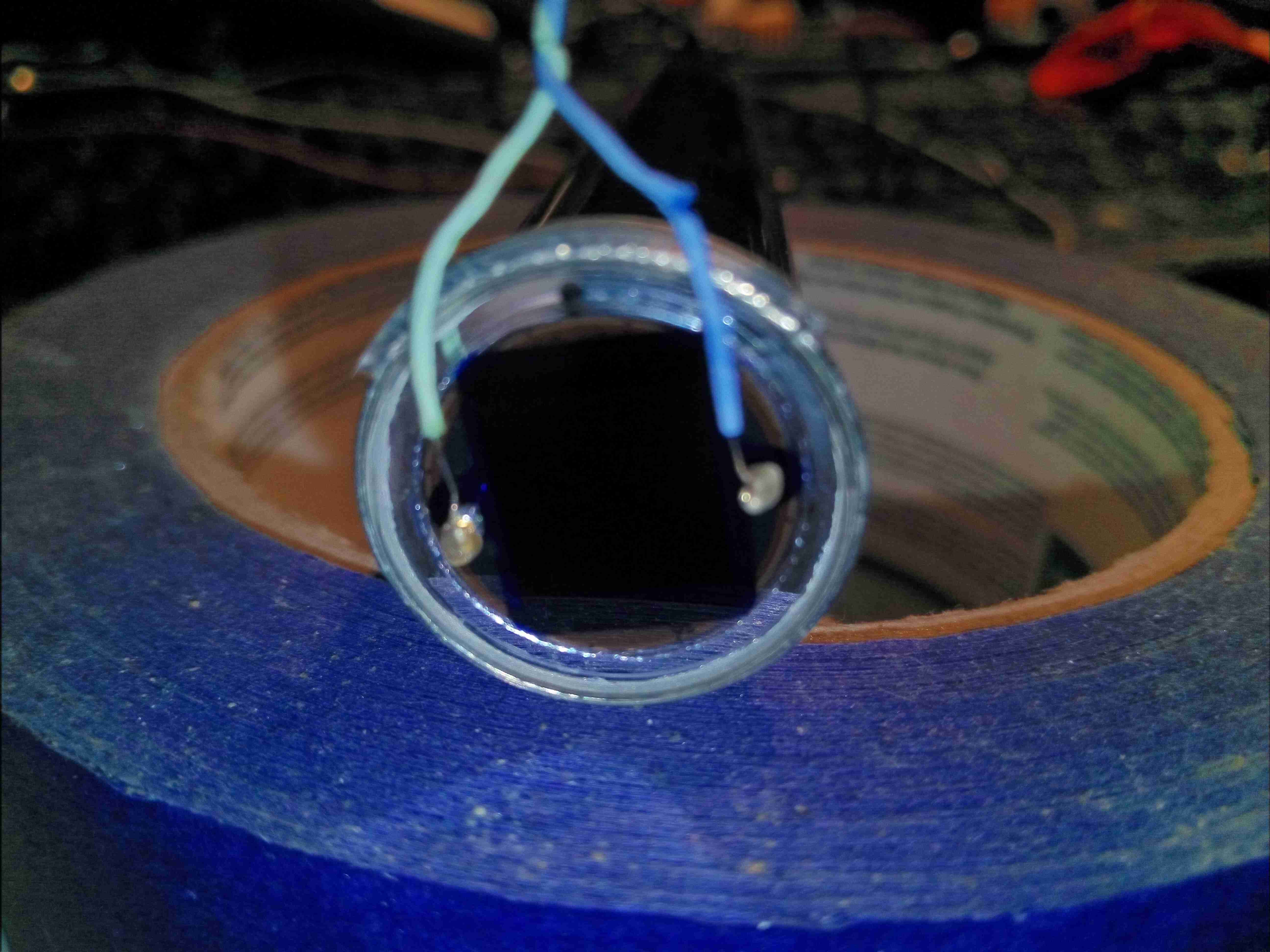
Finally, here’s the target end of the tube. I’m not sure how the wires are attached to the terminals – it certainly isn’t solder, maybe conductive adhesive?
It uses a vertically striped RGB colour filter over the faceplate of an otherwise standard Vidicon imaging tube to segment the scan into corresponding red, green and blue segments. It is used mostly in low-end consumer cameras, though Sony also used it in some moderate cost professional cameras in the 1980s.
Although the idea of using colour stripe filters over the target was not new, the Trinicon was the only tube to use the primary RGB colours. This necessitated an additional electrode buried in the target to detect where the scanning electron beam was relative to the stripe filter. Previous colour stripe systems had used colours where the colour circuitry was able to separate the colours purely from the relative amplitudes of the signals. As a result, the Trinicon featured a larger dynamic range of operation.

I have the service manuals below for the HVP-2000P & the HVP-4000P, which are very similar cameras, so these may be useful to anyone who has one of these!


Posted on 3 Comments

eBay Reverse Parking Sensors Teardown

Parking Sensors Kit
Parking Sensors Kit

This is a cheap kit from eBay, to retrofit an older car with ultrasonic parking sensors. 4 sensors are included in the kit, along with a hole saw to fit them to the bumper. There’s a small controller module, and a display module that fits onto the dash of the car.

Controller Module
Controller Module

Here’s the controller module, with it’s row of connectors along the front. The unit gets it’s power from the reversing light circuit, via the red connector.

Main Controller PCB
Main Controller PCB

Removing a couple of screws allows the PCB to be removed. There’s quite a bit on this board, including 4 tunable inductors for the ultrasonic transducers. There’s a linear voltage regulator on the left which supplies power to the electronics, and a completely unmarked microcontroller.

Electronics Closeup
Electronics Closeup

A closer look at the analogue end of the board shows a JRC4558D dual Op-Amp, and an NXP HEF4052B analogue multiplexer. As the microcontroller is unmarked I have no data for that one.

Dash Display
Dash Display

The dash display is housed in another small plastic box, with bargraphs for each side of the car & an overall distance meter.

Display Module
Display Module

Clearly this is a custom module, with the tapered bargraph LEDs on each side & the 7-segment display in the centre. There’s a beeper which works like every factory-fitted unit does, increasing in rate as the distance closes.

Display PCB
Display PCB

The back of the display module has the driver PCB, with yet another unmarked microcontroller, and a TI 74HC164 serial shift register as a display driver. There’s only 3 wires in the loom from the controller, so some sort of 1-wire protocol must be being used, while I²C is the most likely protocol to be talking to the display driver circuit. There’s also a small switch for muting the beeper.

Posted on Leave a comment

Wireless Energy Management SmartSensor

Cover Removed
Cover Removed

Here’s another random bit of RF tech, I’m told this is a wireless energy management sensor, however I wasn’t able to find anything similar on the interwebs. It’s powered by a standard 9v PP3 battery.

Microcontroller
Microcontroller

System control is handled by this Microchip PIC18F2520 Enhanced Flash microcontroller, this has an onboard 10-bit ADC & nanoWatt technology according to their datasheet. There’s a 4MHz crystal providing the clock, with a small SOT-23 voltage regulator in the bottom corner. There’s a screw terminal header & a plug header, but I’ve no idea what these would be used for. Maybe connecting an external voltage/current sensor & a programming header? The tactile button I imagine is for pairing the unit with it’s controller.

PCB Bottom
PCB Bottom

The bottom of the PCB is almost entirely taken up by a Radiocrafts RC1240 433MHz RF transceiver. Underneath there’s a large 10kΩ resistor, maybe a current transformer load resistor, and a TCLT1600 optocoupler. Just from the opto it’s clear this unit is intended to interface in some way to the mains grid. The antenna is connected at top right, in a footprint for a SMA connector, but this isn’t fitted.

Posted on Leave a comment

First Alert CO-FA-9B Carbon Monoxide Alarm Teardown

CO-FA-9B Alarm
CO-FA-9B Alarm

Here’s another domestic CO Alarm, this one a cheaper build than the FireAngel ones usually use, these don’t have a display with the current CO PPM reading, just a couple of LEDs for status & Alarm.

Rear
Rear

This alarm also doesn’t have the 10-year lithium cell for power, taking AA cells instead. The alarm does have the usual low battery alert bleeps common with smoke alarms though, so you’ll get a fair reminder to replace them.

Internals
Internals

Not much at all on the inside. The CO sensor cell is the same one as used in the FireAngel alarms, I have never managed to find who manufactures these sensors, or a datasheet for them unfortunately.

PCB Top
PCB Top

The top of the single sided PCB has the transformer for driving the Piezo sounder, the LEDs & the test button.

PCB Bottom
PCB Bottom

All the magic happens on the bottom of the PCB. The controlling microcontroller is on the top right, with the sensor front end on the top left.

Circuitry Closeup
Circuitry Closeup

The microcontroller used here is a Microchip PIC16F677. I’ve not managed to find datasheets for the front end components, but these will just be a low-noise op-amp & it’s ancillaries. There will also be a reference voltage regulator. The terminals on these sensors are made of conductive plastic, probably loaded with carbon.

Sensor Cell & Piezo Disc

The expiry date is handily on a label on the back of the sensor, the Piezo sounder is just underneath in it’s sound chamber.

Posted on 10 Comments

Sony PS3 APS-231 Power Supply Voltage Mod

PSU Ratings
PSU Ratings
PSU Ratings

I was recently given a Sony PS3 with a dead disc drive, and since I’m not a console gamer I figured I’d see if there were any handy parts inside. Turns out these units contain a rather nice SMPS, the Sony APS-231 with a high power 12v rail, rated at 23.5A. A bit of searching around discovered a thread on the BadCaps Forums about voltage modding these supplies for a 13.8v output, suitable for my Ham radio gear.
These supplies are controlled by a Sony CXA8038A, for which there is very little information. Active PFC is included, along with synchronous rectification which increases the efficiency of the supply, and in turn, reduces the waste heat output from the rectifiers.

Regulation Section
Regulation Section

Like many of the SMPS units I’ve seen, the output voltage is controlled by referencing it to an adjustable shunt reference, and adjusting the set point of this reference will in turn adjust the output voltage of the supply, this is done in circuit by a single resistor.

Here’s the regulator section of the PSU, with the resistors labelled. The one we’re after changing is the 800Ω one between pins 2 & 3 of the TS2431 shunt reference. It’s a very small 0402 size resistor, located right next to the filter electrolytic for the 5v standby supply circuit. A fine tip on the soldering iron is required to get this resistor removed.

Attachment Points
Attachment Points

Once this resistor is removed from the circuit, a 1KΩ 18-turn potentiometer is fitted in it’s place, from the Anode (Pin 3) to the Ref. (Pin 2) pins of the TS2431 shunt reference. I initally set the potentiometer to be the same 800Ω as the factory set resistor, to make sure the supply would start up at a sensible voltage before I did the adjustment.

Potentiometer
Potentiometer

The pot is secured to the top of the standby supply transformer with a drop of CA glue to stop everything moving around. The supply can now be adjusted to a higher setpoint voltage – 13.8v is about the maxumum, as the OVP cuts the supply out at between 13.9v-14v.

Modded Voltage
Modded Voltage

After doing some testing at roughly 50% of the supply’s rated load, everything seems to be stable, and nothing is heating up more than I’d expect.

Posted on Leave a comment

Mercury 30A Ham Radio SMPS

Mercury 30A SMPS
Mercury 30A SMPS

After having a couple of the cheap Chinese PSUs fail on me in a rather spectacular fashion, I decided to splash on a more expensive name-brand PSU, since constantly replacing PSUs at £15 a piece is going to get old pretty fast. This is the 30A model from Mercury, which seems to be pretty well built. It’s also significantly more expensive at £80. Power output is via the beefy binding posts on the front panel. There isn’t any metering on board, this is something I’ll probably change once I’ve ascertained it’s reliability. This is also a fixed voltage supply, at 13.8v.

Rear Panel
Rear Panel

Not much on the rear panel, just the fuse & cooling fan. This isn’t temperature controlled, but it’s not loud. No IEC power socket here, the mains cable is hard wired.

Main Board
Main Board

Removing some spanner-type security screws reveals the power supply board itself. Everything on here is enormous to handle the 30A output current at 13.8v. The main primary side switching transistors are on the large silver heatsink in the centre of the board, feeding the huge ferrite transformer on the right.

Transformer
Transformer

The transformer’s low voltage output tap comes straight out instead of being on pins, due to the size of the winding cores. Four massive diodes are mounted on the black heatsinks for output rectification.


SMPS Controller
SMPS Controller

The supply is controlled via the jelly bean TL494 PWM controller IC. The multi-turn potentiometer doesn’t adjust the output voltage, more likely it adjusts the current limit.

Standby Supply
Standby Supply

Power to initially start the supply is provided by a small SMPS circuit, with a VIPer22A Low Power Primary Switcher & small transformer on the lower right. The transformer upper left is the base drive transformer for the main high power supply.

Posted on Leave a comment

Behringer DEQ2496 Mastering Processor

Bootscreen
Bootscreen

I was recently given this unit, along with another Behringer sound processor to repair, as the units were both displaying booting problems. This first one is a rather swish Mastering Processor, which has many features I’ll leave to Behringer to explain 😉

Input Board & Relays

All the inputs are on the back of this 19″ rackmount bit of kit, nothing much on this PCB other than the connectors & a couple of switching relays.

Main Processor PCB
Main Processor PCB

All the magic is done on the main processor PCB, which is host to 3 Analog Devices DSP processors:

ADSP-BF531 BlackFin DSP. This one is probably handling most of the audio processing, as it’s the most powerful DSP onboard at 600Mhz. There’s a ROM on board above this for the firmware & a single RAM chip. On the right are a pair of ADSP-21065  DSP processors at a lower clock rate of 66MHz. To the left is some glue logic to interface the user controls & dot-matrix LCD.

PSU Module
PSU Module

The PSU in this unit is a pretty standard looking SMPS, with some extra noise filtering & shielding. The main transformer is underneath the mu-metal shield in the centre of the board.

Posted on 12 Comments

Panasonic NV-M5 VHS Camcorder Teardown

Overview

Panasonic NV-M5 Camera

Time foe some more retro tech! This is a 1980’s vintage CCD-based VHS camcorder from Panasonic, the NV-M5. There are a lot of parts to one of these (unlike modern cameras), so I’ll split this post into several sections to make things easier to read (and easier to keep track of what I’m talking about :)).

Left Side
Left Side

The left side of the camera holds the autofocus, white balance, shutter speed & date controls.

Left Side Controls
Left Side Controls
Lens Adjustments
Lens Adjustments

The lens is fully adjustable, with either manual or motorized automatic control.

Rear Panel
Rear Panel

The back panel has the battery slot, a very strange looking DC input connector, remote control connector & the earphone jack.

Top Controls
Top Controls

The top panel of the camera holds the main power controls, manual tape tracking & the tape transport control panel.

Viewfinder
Viewfinder

The viewfinder is mounted on a swivel mount. There’s a CRT based composite monitor in here. Hack ahoy!

Camera Section

Process Board Assembly

Here’s the camera section of the camcorder, and is totally packed with electronics! There’s at least half a dozen separate boards in here, all fitted together around the optics tube assembly.

AWB PCB
AWB PCB

On the top of the assembly is the Automatic White Balance PCB. Many adjustments here to get everything set right. Not much on the other side of this board other than a bunch of Op-Amps. The iris stepper motor is fitted in a milled opening in the PCB, this connects to one of the other PCBs in the camera module.

AWB Sensor
AWB Sensor

Here’s the AWB sensor, mounted next to the lens. I’m not all to certain how this works, but the service manual has the pinout, and there are outputs for all the colour channels, RGB. So it’s probably a trio of photodiodes with filters.

Focus & Zoom Motors
Focus & Zoom Motors

Focus & Zoom are controlled with a pair of DC gear motors. The manual operation is feasible through the use of slip clutches in the final drive pinion onto the lens barrel.

Process Board
Process Board

The main camera section process board is above. This board does all the signal processing for the CCD, has the bias voltage supplies and houses the control sections for the motorized parts of the optics assembly. There are quite a few dipped Tantalum capacitors on pigtails, instead of being directly board mounted. This was probably done due to space requirements on the PCB itself.2016-08-20_13-40-11_000357

Under the steel shield on this board is some of the main signal processing for the CCD.

Optics Assembly
Optics Assembly

The back of the optics tube is a heavy casting, to supress vibration. This will be more clear later on.

Position Sensor Flex

The position of the lens elements is determined by reflective strips on the barrel & sensors on this flex PCB.

Sub Process Board
Sub Process Board

There’s another small board tucked into the side of the tube, this hooks into the process PCB.

Process Delay Line
Process Delay Line

According to the schematic, there’s nothing much on this board, just a delay line & a few transistors.

Piezo Focus Disc
Piezo Focus Disc

Here’s the reason for the heavy alloy casing at the CCD mounting end of the optics: the fine focus adjustment is done with a piezoelectric disc, the entire CCD assembly is mounted to this board. Applying voltage to the electrodes moves the assembly slightly to alter the position of the CCD. The blue glass in the centre of the unit is the IR filter.

IR Relective Sensors

The barrel position sensors are these IR-reflective type.

Iris Assembly
Iris Assembly

The iris is mounted just before the CCD, this is controlled with a galvanometer-type device with position sensors incorporated.

Iris Opening
Iris Opening

Pushing on the operating lever with the end of my screwdriver opens the leaves of the iris against the return spring.

Tape Transport & Main Control

Main Control Board
Main Control Board

Tucked into the side of the main body of the unit is the main system control board. This PCB houses all the vital functions of the camera: Power Supply, Servo Control, Colour Control,Video Amplifiers, etc.

Tape Drum
Tape Drum

Here’s the main tape transport mechanism, this is made of steel & aluminium stampings for structural support. The drum used in this transport is noticeably smaller than a standard VHS drum, the tape is wrapped around more of the drum surface to compensate.

Tape Transport
Tape Transport

The VHS tape sits in this carriage & the spools drive the supply & take up reels in the cartridge.

Main Control PCB
Main Control PCB

Here’s the component side of the main control PCB. This one is very densely packed with parts, I wouldn’t like to try & troubleshoot something like this!

Main PCB Left
Main PCB Left

The left side has the video head amp at the top, a Panasonic AN3311K 4-head video amp. Below that is video processing, the blue components are the analogue delay lines. There are a couple of hybrid flat-flex PCBs tucked in between with a couple of ICs & many passives. These hybrids handle the luma & chroma signals.
Top left is the capstan motor driver a Rohm BA6430S. The transport motors are all 3-phase brushless, with exception of the loading motor, which is a brushed DC type.

Delay Line
Delay Line

Here’s what is inside the delay lines for the analogue video circuits. The plastic casing holds a felt liner, inside which is the delay line itself.

Internal Glass
Internal Glass

The delay is created by sending an acoustic signal through the quartz crystal inside the device by a piezoelectric transducer, bouncing it off the walls of the crystal before returning it to a similar transducer.

Main PCB Centre
Main PCB Centre

Here’s the centre of the board, the strange crystal at bottom centre is the clock crystal for the head drum servo. Why it has 3 pins I’m not sure, only the two pins to the crystal inside are shown connected on the schematic. Maybe grounding the case?
The main servo controls for the head drum & the capstan motor are top centre, these get a control signal from the tape to lock the speed of the relative components.

Main PCB Right
Main PCB Right

Here’s the right hand side. The main power supply circuitry is at top right, with a large can containing 4 switching inductors & a ferrite pot core transformer. All these converters are controlled by a single BA6149 6-channel DC-DC converter controller IC via a ULN2003 transistor array.
The ceramic hybrid board next to the PSU has 7 switch transistors for driving various indicator LEDs.
The large tabbed IC bottom centre is the loading motor drive, an IC from Mitsubishi, the M54543. This has bidirectional DC control of the motor & built in braking functions. The large quad flat pack IC on the right is the MN1237A on-screen character generator, with the two clock crystals for the main microcontroller.

Erase Head
Erase Head

The full erase head has it’s power supply & oscillator on board, applying 9v to this board results in an AC signal to the head, which erases the old recording from the tape before the new recording is laid down by the flying heads on the drum.

Audio Control PCB
Audio Control PCB

The Audio & Control head is connected to this PCB, which handles both reading back audio from the tape & recording new audio tracks. The audio bias oscillator is on this board, & the onboard microphone feeds it’s signal here. The control head is fed directly through to the servo section of the main board.

Drum Motor
Drum Motor

The motor that drives the head drum is another DC brushless 3-phase type.

Hall Sensors
Hall Sensors

These 3 Hall sensors are used by the motor drive to determine the rotor position & time commutation accordingly.

Stator
Stator

The stator on this motor is of interesting construction, with no laminated core, the coils are moulded into the plastic holder. The tach sensor is on the side of the stator core. This senses a small magnet on the outside of the rotor to determine rotational speed. For PAL recordings, the drum rotates at 1500 RPM.

Motor Removed
Motor Removed

Not much under the stator other than the bearing housing & the feedthrough to the rotary transformer.

Head Disc
Head Disc

The heads are mounted onto the top disc of the drum, 4 heads in this recorder. The signals are transmitted to the rotating section through the ferrite rotary transformer on the bottom section.

Head Chip
Head Chip

The tiny winding of the ferrite video head can just about be seen on the end of the brass mounting.

Capstan Motor Components

The capstan motor is similar to the drum motor, only this one is flat. The rotor has a ferrite magnet, in this case it wasn’t glued in place, just held by it’s magnetic field.

Capstan Motor Stator

The PCB on this motor has a steel backing to complete the magnetic circuit, the coils for the 3 motor phases are simply glued in place. The Hall sensors on this motor are placed in the middle of the windings though.
Again there is a tach sensor on the edge of the board that communicates the speed back to the controller. This allows the servo to remain locked at constant speed.

Viewfinder

Viewfinder Assembly
Viewfinder Assembly

As usual with these cameras, this section is the CRT based viewfinder. These units take the composite signal from the camera to display the scene. This one has many more pins than the usual viewfinder. I’ll hack a manual input into this, but I’ll leave that for another post.

Viewfinder Circuits
Viewfinder Circuits

Being an older camera than the ones I’ve had before, this one is on a pair of PCBs, which are both single-sided.

Main Viewfinder Board

The main board has all the power components for driving the CRT & some of the adjustments. The main HV flyback transformer is on the right. This part creates both the final anode voltage for the tube & the focus/grid voltages.

Viewfinder Control PCB Top

The viewfinder control IC is on a separate daughter board in this camera, with two more controls.

Control IC
Control IC

The control IC is a Matsushita AN2510S, this has all the logic required to separate the sync pulses from the composite signal & generate an image on the CRT.

Viewfinder CRT Frame

The recording indicator LEDs are mounted in the frame of the CRT & appear above the image in the viewfinder.

Viewfinder CRT With Yoke

Here the CRT has been separated from the rest of the circuitry with just the deflection yoke still attached.

M01JPG5WB CRT
M01JPG5WB CRT

The electron gun in this viewfinder CRT is massive in comparison to the others that I have seen, and the neck of the tube is also much wider. These old tubes were very well manufactured.

Viewfinder Optics
Viewfinder Optics

A simple mirror & magnifying lens completes the viewfinder unit.

Modular He-Ne Laser Power Supply

Description and Schematic

SG-HM2 is a modular He-Ne laser power supply based on IC-HI1 with some minor enhancements. The first version is for laser tubes up to approximately 1 mW (2 mW with trivial modifications) but it should be straightforward to go to 5 mW or even higher power tubes by replacing the SG-HM2 HV Module (HVM2-1) with one with a higher voltage and current rating, along with a higher power MOSFET and minor component value changes to the Control Module (suggestions below). I have added an adjustment for tube current, a current limiting resistor and Zener to protect against output short circuits, an enable input (ground to turn on), a bleeder resistor to virtually eliminate the shock hazard after the power supply is turned off, and power and status LEDs.

  • Get the schematic for SG-HM2 (1 mW version) in PDF format: [download id=”5610″]

Modifying SG-HM2 for Higher Power He-Ne Laser Tubes

The following are guidelines for modifying SG-HM2 to drive various power He-Ne lasers. The PCB layout below with two versions of the HV Module should accommodate He-Ne laser tubes up to 10 mW. All assume input of around 12 V though a higher power system can generally run lower power lasers at reduced input voltage. If operation at rated power on another input voltage is desired, the number of turns on the inverter transformer can be adjusted accordingly. As noted above, the 1 mW HV Module (HVM2-1) should run tubes up to about 2 mW, though increasing the µF values of some of the HV capacitors may be desirable to reduce ripple at the higher tube current. Minor changes may also be needed in the components on the SG-HM2 Control Module including using a higher power MOSFET for Q1 and reducing the values of R7 and/or R8 for the higher tube current. Or, just populate the Control Module with Q1 being an IRF644, R7 being 150 ohms, and R8 being 750 ohms for compatibility with all the HV modules. For that matter, the HVM2-5 PCB HV Module should be usable with lower power lasers.

SG-HM2 Inverter Transformer

The inverter transformer for HVM2-1 is wound on a ferrite pot core with a small air-gap (about 0.005″). It is 18 mm in diameter by 11 mm high. While specified to use a 9 turn primary and 450 turn secondary, these values can be adjusted somewhat to handle various input and output requirements. Don’t go much lower on the primary as this may result in core saturation. The 9/450 transformer should be fine for 1 to 2 mW He-Ne laser tubes running on 8 to 15v DC input. With 9/300, it will operate on about 12 to 20v DC. Increasing the number of secondary turns (e.g., 9/600) may result in operation on a slightly lower input voltage, but probably not by much. The 9/450 transformer may even run He-Ne laser tubes larger than 2 mW but I haven’t yet tested this since I haven’t built a prototype of HVM2-5 as yet.

It doesn’t matter very much whether the primary (P) is wound first or the secondary (S) is wound first though the former appears to work slightly better, running the tube at about 8v DC input instead of 9v DC input for the same 9/450 transformer. P over S is slightly easier to wind since the primary doesn’t get in the way and increase the lumpiness of the secondary layers. However, with S over P, insulation is somewhat less critical since the HV lead is out away from anything else. With the P over S, additional insulation is needed between them. Also, since the primary coil is larger diameter, it will have more resistance and there will be greater inter-winding capacitance (though probably not significant). The secondary should be constructed as multiple layers of about 50 or 60 turns each, with insulating tape between layers. Each should be wound in as close to a single layer as possible with alternating layers staggered to prevent arc-over. This doesn’t have to be perfect but try to go gradually from one side to the other to keep wires at high relative potential away from each other. Make sure the HV output leads (particularly the one away from the dot) are well insulated as they exit the transformer. And, as noted, if the primary is over the secondary, there must be high voltage insulation between them. The peak output voltage when the MOSFET turns off (the flyback pulse) may be more than 5 times higher than what would be expected from the DC input voltage and the turns-ratio alone – several kV and this *will* try to find a path to ground! There are more detailed transformer construction instructions in the next section.

Note that this transformer is slightly larger physically than the one from IC-HI1. This is for two reasons: (1) It is easier to wind with more space and a larger wire size for the secondary, and (2) continuous operation should be possible with 2 mW laser tubes, which might have been marginal with the original transformer used in IC-HI1. A by-product of the larger core is that its 9 turn primary should be roughly equivalent to the 12 turn primary of the smaller core in terms of inductance and core saturation limitations.

Interestingly, a similar transformer found in a different commercial power supply, had no insulating tape anywhere. It would appear that with very precise machine-wound HV secondary, done first, the voltage is distributed so uniformly that this is unnecessary.

I’ve now built and tested several transformers in IC-HI1, removing the original transformer and installing socket pins so either the original or an adapter board can be plugged in. This setup is then equivalent to SG-HM2 with the HVM2-1 HV Module. The minimum input voltage values that follow are when driving a 0.5 mW He-Ne laser tube:

*The number of turns on the original (#1) is not really known exactly and may be lower or higher by up to 25 percent based on the measured secondary resistance (45 ohms) and estimated wire size (somewhere between #38 and #40. (Even with the larger wire, the amount of bobbin area taken up by the wire is less than 50 percent so it should fit even with many layers of insulating tape. The transformer is Epoxy impregnated and likely to be impossible to disassemble into any form that can be analyzed!)

All of these transformers will drive He-Ne laser tubes of up to at least 2.5mW using the equivalent of the HVM2-1 HV Module which is part of IC-HI1. Even with the 2.5mW tube, the minimum operating voltage was only about 0.5v higher than for the 0.5mW tube. There is a good chance they would drive even larger He-Ne laser tubes (though possibly at a slightly higher input voltage) but I don’t dare try using the existing HV circuitry as it might not survive for long. I suspect that transformers #4, #5, and #6 would run on an input voltage of less than 8v DC but the salvaged cores I am using have a larger air-gap than might be optimal and I don’t have anything to reduce it without heavy losses. They attempt to start the tube at around 6v DC but are unable to maintain it and flicker rapidly. (#2 and #3, which use the same style core, would also benefit somewhat.) Operation using #1 and #5 is virtually identical, with the original running at perhaps 0.5v DC less input. I expect they would be even more identical if the air-gap on #5 were smaller, and #6 with its smaller air-gap does indeed run at the lower input voltage. I haven’t actually confirmed that anything blows up above the maximum voltages listed above, which were arbitrarily chosen. But I am guessing that bad things might happen at some point. 🙂

I have also constructed a transformer which will need to be used with HVM2-5: 12/1200, P over S, on a 30×19 pot core. I will also construct a 9/900. S over P, on a 30×19 pot core (or on a 26×16 if I can find one). Testing of these will have to await an HVM2-5 prototype.

SG-HM2 Transformer Construction

Here are details on construction of the inverter transformer for SG-HM2. With all parts and tools on hand, it takes about an hour start to finish. Only a small portion of this time is in the actual winding (at least if a coil winding machine is used). Most of the time is spent in adding the insulation tape and terminating the leads. After constructing a few of these, it does go quicker. 🙂

Step-by-step instructions are provided for the HVM2-1 transformer. The changes needed for HVM2-5 are summarized at the end of this section. Some sort of coil winding machine is almost essential as #40 wire is extremely thin and easy to break. (Anything larger than #40 will not fit on the bobbin.) It doesn’t have to be fancy. Mine is probably 50 years old of the type that is (used to be?) advertised in the back of electronics magazines. However, a couple of spindles – one that is fixed or free to rotate for the wire supply and the other which can be turned for the coil being wound – are really all that are needed. Don’t use any sort of powered approach though (unless you have a *real* professional coil winder!) as it is all too easy to break the wire if there is no tactile feedback to detect snags.

  1. Parts required for T101 of HVM2-1:
    • 18×11 mm (1811) ferrite pot core with a small air-gap (no more than 0.005″) or no air-gap, and a single section bobbin. These are available from several manufacturers but surplus or salvaged cores may be easier to obtain. Radio Shack used to have a “ferrite kit” which included a variety of sizes of cores (only 1 each though so you’d have to buy two kits and there were no bobbins!). I doubt the kit still exists though.
    • Approximately 1.5 feet of #28 magnet wire for the primary (9 turns wound first) and approximately 60 feet of #40 magnet wire for the secondary (450 turns wound on top of the primary). I found both these size wire in various solenoids and relays I’ve discombobulated. 🙂 Wire sizes aren’t critical but these are known to fit and the #40 can be handled with a reasonable chance of not breaking.
    • Sleeving to protect the primary wires where they leave transformer. I used approximately 2″ of insulation (each lead) from the individual wires in some 25 pair phone cable.
    • Wirewrap wire or other thin insulated wire to terminate the secondary wires where they leave the transformer.
    • Insulating tape. 1 mil Mylar or similar is desirable. However, I’ve found that thin clear (non-reinforced) packing tape does an adequate job, though it probably doesn’t have as much dielectric strength as real insulating tape so additional layers are required. It will also likely not stand up to overheating too well. Electrical tape is way too thick and would prevent enough turns from fitting.
    • A piece of Perf. board with holes on 0.1″ centers, 0.8″x0.8″. There should be 7 rows of holes each way so that one hole lines up in the center.
    • A Nylon 4-40 screw and nut to fasten the transformer to the board.
    • Four (4) machined-type IC socket pins or something similar to use as terminals.
  2. Wind the primary:
    • Slip a piece of sleeving over the start of the primary wire and position the sleeving so it extends about 1/2 turn inside the bobbin on the left side.
    • Wrap exactly 9 turns of this wire clockwise around the bobbin, left to right. The wires should enter and exit on the same angular position (slot) of the bobbin on opposite sides.
    • Slip another piece of sleeving over the wire end exiting the bobbin so that it too is about 1/2 turn inside the bobbin.
    • Wrap 1.5 to 2 turns of tape tightly over the primary winding to secure and insulate it.
  3. Wind the secondary:
    • Strip 1/8″ or so from the end of a 2″ piece of wire-wrap wire and solder the start of the wire for the secondary winding to it. Make sure the insulation on the fine magnet wire has been removed – usually just heating it while soldering will do this. Leave an inch or so of the magnet wire extending from the connection so that continuity can be confirmed with a multimeter, then snip it off. Install this in the opposite slot of the bobbin also on the left side with about 1/4″ of insulation inside the bobbin against the side and separated from the primary. Leave a little slack in the fine secondary wire so that slight motion won’t break it. Add a small piece of tape to protect and insulate this connection.
    • Using your coil winding machine (you do have one, correct?), build up the secondary in layers of about 50 to 75 turns in a counter-clockwise direction (bobbin being rotated clockwise). A single layer of wire won’t fit in the 1/8″ or so available (in the 18×11 mm core bobbin) so there will have to be some overlap. But, do this several times across the layer so that any given wire won’t be next to one with a much different voltage. In other words, wind a few turns and back up so that there will in essence be multiple sub-windings of 5 or 10 turns, repeated several times across the layer. Keep the wire at least 1/32″ away from either edge of the bobbin.
    • After each full layer or wire, add just over 1 layer of insulating tape making sure it covers the entire width of the bobbin. There should be just enough overlap to assure there is at least 1 layer of insulation but not much more as excessive tape will end up taking up too much space.The entire 450 turn winding will then require 6 to 9 full layers. Add another layer of insulating tape over the last winding layer leaving the wire end exposed.
    • Terminate the end of the secondary winding with another piece of thin wire by soldering as above. Confirm continuity with a multimeter. For the 450 turn secondary, the resistance should be about 60 ohms. Add a piece of thicker sleeving over this at the HV end if space is available. Else, use some bits of tape to insulate the wirewrap wire lead from the core and exposed inner layers that it may come near as it exits out the side of the bobbin. Add another layer of tape to secure the lead in place.
    • Add several more layers of insulating tape to complete the bobbin assembly.
  4. Prepare the mounting board:
    • Widen the center hole to 7/64″ to accommodate a 4-40 nylon screw.
    • Widen the holes at the 4 corners of the board to accept the 4 IC socket pins (if used) as a press-fit or glue them in place with 5 minute Epoxy or SuperGlue.
  5. Final assembly:
    • Install the ferrite pot core halves to the bobbin taking care not to crunch any of the wires. Orient it so that the primary and secondary leads are conveniently located with respect to the 4 pins, e.g., primary start: bottom left; primary end: top left, secondary start: bottom right; and primary end: top right.
    • Use the nylon 4-40 screw and nut to *gently* secure the transformer to the mounting board. The head of the 4-40 screw should be underneath the board. Don’t over-tighten or it may crack the core, especially if it has an air-gap in the middle.
    • Carefully remove the insulation from the ends of the wires. The secondary wires will still be fragile even with the wirewrap wire terminations. For the magnet wire, the easiest way to remove the insulation is to burn it off with a match or hot soldering iron and then clean with fine sandpaper.
    • Push the wires into their respective socket pins. (The wirewrap wires are too thin to be secure but they will make adequate contact for testing.)
    • Use a multimeter to confirm continuity of the primary (close to 0 ohms) and secondary (about 50 to 75 ohms).
  6. Testing:
    • Install the transformer in you HV Module. Attach a He-Ne laser tube and ballast resistor.
    • Power up on an variable DC power supply and check for reliable starting and stable operation. Adjust the core gap if needed. A smaller gap may result in more operating power available at a given input voltage. A larger gap will result in attempts to start on a lower input voltage. Somewhere around 0.005″ is probably a good compromise.
    • After testing the transformer (and adjusting the core gap if needed), use some adhesive to secure the pot core sections and to protect the transformer leads. Solder the leads into the socket pins.

The final result is shown on an adapter below:

Photo of SG-HM2 HVM2-1 Transformer being Tested in IC-HI1

The instructions for winding the HVM2-5 transformer are similar except for the dimensions, wire sizes and lengths, and number of turns for the primary and secondary:

  • Differences in parts list for T501 of HVM2-5 compared to T101 of HVM2-1:
    • 26×16 mm (2616) ferrite pot core with a small air-gap (no more than 0.005″) or no air-gap, and a single section bobbin.
    • Approximately 2.0 feet of #26 magnet wire for the primary (12 turns wound first) and approximately 75 to 120 feet of #40 magnet wire for the secondary (600 or 900 turns wound on top of the primary).
    • A piece of Perf. board with holes on 0.1″ centers, 1.0″x1.0″. There should be 9 rows of holes each way so that one hole lines up in the center.
    • A Nylon 10-32 screw and nut to fasten the transformer to the board.

Since the peak voltage on the HVM2-5 secondary may be 2 to 3 times higher than for HVM2-1, extra insulation and clearances will be required on the secondary.

SG-HM2 Printed Circuit Board Layout

A printed circuit board layout is also available. The Control Module is 2″x1.2″. The HV Modules are 3.6″x1.2″ and 4.5″x1.8″ for the 1 mW (HVM2-1) and 5 mW (HVM2-5), respectively. The Control and HV Modules are connected by a 2 pin cable for transformer drive and a 3 pin cable for current sensing from the laser tube. The two boards can easily be merged if desired.

The layout of the 3 PCBs may be viewed as a GIF file (draft quality) as below:

Sam's Modular He-Ne Laser Power Supply 2 PCB Layout
Sam’s Modular He-Ne Laser Power Supply 2 PCB Layout

.

A complete PCB artwork package for SG-HM2 (all PCBs on one sheet) may be downloaded in standard (full resolution 1:1) Gerber PCB format (zipped) as [download id=”5612″]

The Gerber files include the component side copper, soldermask, and silkscreen; solder side copper and soldermask, and drill control artwork. The original printed circuit board CAD files and netlist (in Tango PCB format) are provided so that the circuit layout can be modified or imported to another system if desired. The text file ‘sghm2.doc’ (in sghm2grb.zip) describes the file contents in more detail.

Note: The netlist does NOT include wiring for the HVM2-5 HV Module. Also, part numbers on the HVM2-5 PCB actually begin with a “5” instead of a “1” since Tango PCB will not allow duplicate part numbers on the same layout.

He-Ne Laser Safety

As with *any* laser, proper precautions must be taken to avoid any possibility of damage to vision. The types of He-Ne lasers mostly dealt with in this document are rated Class II, IIIa, or the low end of IIIb (see the section: Laser Safety Classifications. For most of these, common sense (don’t stare into the beam) and fairly basic precautions suffice since the reflected or scattered light will not cause instantaneous injury and is not a fire hazard.

However, unlike those for laser diodes, He-Ne power supplies utilize high voltage (several kV) and some designs may be potentially lethal. This is particularly true of AC line powered units since the power transformer may be capable of much more current than is actually required by the He-Ne laser tube – especially if it is home built using the transformer from some other piece of equipment (like an old tube type console TV or that utility pole transformer you found along the curb) which may have a much higher current rating.

The high quality capacitors in a typical power supply will hold enough charge to wake you up – for quite a while even after the supply has been switched off and unplugged. Depending on design, there may be up to 10 to 15 kV or more (but on very small capacitors) if the power supply was operated without a He-Ne tube attached or it did not start for some reason. There will likely be a lower voltage – perhaps 1 to 3 kV – on somewhat larger capacitors. Unless significantly oversized, the amount of stored energy isn’t likely to be enough to be lethal but it can still be quite a jolt. The He-Ne tube itself also acts as a small HV capacitor so even touching it should it become disconnected from the power supply may give you a tingle. This probably won’t really hurt you physically but your ego may be bruised if you then drop the tube and it then shatters on the floor!

However, should you be dealing with a much larger He-Ne laser, its power supply is going to be correspondingly more dangerous as well. For example, a 35 mW He-Ne tube typically requires about 8 mA at 5 to 6 kV. That current may not sound like much but the power supply is likely capable of providing much more if you are the destination instead of the laser head (especially if it is a home-made unit using grossly oversized parts)! It doesn’t take much more under the wrong conditions to kill.

After powering off, use a well insulated 1M resistor made from a string of ten 100K, 2 W metal film resistors in a glass or plastic tube to drain the charge – and confirm with a voltmeter before touching anything. (Don’t use carbon resistors as I have seen them behave funny around high voltages. And, don’t use the old screwdriver trick – shorting the output of the power supply directly to ground – as this may damage it internally.)

And only change electrical connections or plug/unplug connectors with power OFF, being aware of the potential for stored charge. In particular, the aluminium cylinder of some HeNe laser heads is the negative return for the tube current via a spring contact inside the rear end-cap. So, pulling off the rear end-cap while the laser is powered will likely make YOU the negative return instead! You will probably then bounce off the ceiling while the laser bounces off the floor, which can easily ruin your entire day in more ways than one. 🙁 🙂 This connection scheme is known to be true for most JDS Uniphase and many Melles Griot laser heads, but may apply to others as well.

Now, for some first-hand experience:

(From: Doug (dulmage@skypoint.com).)

Well, here’s where I embarrass myself, but hopefully save a life…

I’ve worked on medium and large frame lasers since about 1980 (Spectra-Physics 168’s, 171’s, Innova 90’s, 100’s and 200’s – high voltage, high current, no line isolation, multi-kV igniters, etc.). Never in all that time did I ever get hurt other than getting a few retinal burns (that’s bad enough, but at least I never fell across a tube or igniter at startup). Anyway, the one laser that almost did kill me was also the smallest that I ever worked on.

I was doing some testing of AO devices along with some small cylindrical HeNe tubes from Siemens. These little coax tubes had clips for attaching the anode and cathode connections. Well, I was going through a few boxes of these things a day doing various tests. Just slap them on the bench, fire them up, discharge the supplies and then disconnect and try another one. They ran off a 9 VDC power supply.

At the end of one long day, I called it quits early and just shut the laser supply off and left the tube in place as I was just going to put on a new tube in the morning. That next morning, I came and incorrectly assumed that the power supply would have discharged on it own overnight. So, with each hand I stupidly grab one clip each on the laser to disconnect it. YeeHaaaaaaaaa!!!!. I felt like I had been hid across my temples with a two by four. It felt like I swallowed my tongue and then I kind of blacked out. One of the guys came and helped me up, but I was weak in the knees, and very disoriented.

I stumbled around for about 15 minutes and then out of nowhere it was just like I got another shock! This cycle of stuff went on for about 3 hours, then stopped once I got to the hospital. I can’t even remember what they did to me there. Anyway, how embarrassing to almost get killed by a HeNe laser after all that other high power stuff that I did. I think that’s called ‘irony’.

Comments on HeNe Laser Safety Issues

(Portions from: Robert Savas (jondrew@mail.ao.net).)

A 10 mw HeNe laser certainly presents an eye hazard.

According to American National Standard, ANSI Z136.1-1993, table 4 Simplified Method for Selecting Laser Eye Protection for Intrabeam Viewing, protective eyewear with an attenuation factor of 10 (Optical Density 1) is required for a HeNe with a 10 milliwatt output. This assumes an exposure duration of 0.25 to 10 seconds, the time in which they eye would blink or change viewing direction due the uncomfortable illumination level of the laser. Eyeware with an attenuation factor of 10 is roughly comparable to a good pair of sunglasses (this is NOT intended as a rigorous safety analysis, and I take no responsibility for anyone foolish enough to stare at a laser beam under any circumstances). This calculation also assumes the entire 10 milliwatts are contained in a beam small enough to enter a 7 millimeter aperture (the pupil of the eye). Beyond a few meters the beam has spread out enough so that only a small fraction of the total optical power could possible enter the eye.

Posted on 1 Comment

eBay High Voltage DC-DC Converter Module

High Voltage DC-DC
High Voltage DC-DC

Going through eBay recently looking for parts for a couple of CRT-based projects, I came across these DC-DC converters.
Apparently rated from 45-390v DC output at 200mA, these should be ideal for driving some of the electrodes (focus, screen, grid) in a CRT.
Above is the top of the board, input voltage header on the left, output voltage adjust in the centre & output voltage header on the right.
This module has a mini-automotive fuse, at 10A for input protection.
On the heatsink is mounted the main switching MOSFET, a RU7088R from Ruichips. This FET is fairly heavily rated at 70v 80A, with 6.5mΩ on-resistance.

PCB Bottom
PCB Bottom

The bottom of the board has the control components, with a pair of ICs. Unfortunately the numbers have been scrubbed off, so no identification here. The output from the transformer is rectified with a single large SMD diode on the left side of the board.
There’s also plenty of isolation gap between the HV output trace & the low voltage logic side of the circuit, the two being bridged only by a resistive divider for output voltage measurement.

Posted on Leave a comment

6-Point Ignition Transformer

Ignition Transformer

Here’s a quick teardown of an ignition transformer, used on gas fired ovens & hobs.  This unit takes mains 240v AC & uses a transformer to step the voltage to several kV, at a low current to ignite the burners.

Bottom
Bottom

The transformer section is completely potted in Epoxy resin for insulation, but the driver circuitry is exposed, with a pair of leads from the primary winding exposed

Driver PCB
Driver PCB

The drive is very simple. The incoming AC flows through a series resistor through a half-wave rectifier to charge up a 2.2µF film capacitor. Once the voltage on the capacitor reaches a certain level, a DIAC in series with the transformer primary fires, discharging the capacitor through the primary.
The current spike induces a very high voltage on the secondary winding, this then arcs across a gap in the gas flow to start ignition.

Posted on Leave a comment

De La Rue Coin Counting Machine

Here’s some teardown photos of an old De La Rue coin counter, used in businesses for rapid counting of change into large bags.

Mechanism
Mechanism

An overview of the whole mechanical system of the counter. Coins are loaded into the drum at the rear of the machine, which sorts them into a row for the rubber belt to pick up & run through the counter. The coin type to be sorted is selected by turning the control knobs on the right.
The control knobs adjust the width & height of the coin channel so only the correct sized coins will be counted.

PSU & Switching
PSU & Switching

The counter is driven by a basic AC induction motor, the motor power relay & reversing relay is on this PCB, along with the 5v switching supply for the main CPU board.
The SMPS on this board looks like a standard mains unit, but it’s got one big difference. Under the frame next to the main motor is a relatively large transformer, with a 35v output. This AC is fed into the SMPS section of the PSU board to be converted to 5v DC for the logic.
I’m not sure why it’s been done this way, and have never seen anything similar before.
The edge of the coin channel can be seen here, the black star wheel rotates when a coin passes & registers the count.

Controller PCB
Controller PCB

Here’s the main controller PCB, IC date codes put the unit to about 1995. The main CPU is a NEC UPD8049HC 8-bit micro, no flash or EEPROM on this old CPU, simply mask ROM. Coin readout is done on the 4 7-segment LED displays. Not much to this counter, it’s both electronically & mechanically simple.

Counter Sensor
Counter Sensor

Coin counting is done by the star wheel mentioned above, which drives the interrupter disc on this photo-gate. The solenoid locks the counter shaft to prevent over or under counting when a set number of coins is to be counted.

Motor Run Capacitor
Motor Run Capacitor

Under the frame, here on the left is the small induction motor, only 6W, 4-pole. The run cap for the motor is in the centre, and the 35v transformer is just visible behind it.

Main Motor Drive
Main Motor Drive

Main drive to the coin sorting mech is through rubber belts, and bevel gears drive the coin drum.

Posted on 2 Comments

Fire Angel CO-9D Carbon Monoxide Detector Teardown

Fire Angel CO-9D CO Detector

This detector has now been retired from service since it’s a fair bit out of date. So here’s the teardown!

Information
Information

Unlike older detectors, this unit has a built in battery that never needs replacing during the life of the sensor, so once the unit reaches it’s expiry date it’s just trashed as a whole.

Cover Removed
Cover Removed

4 screws hold the cover on, here’s the internals of the detector. There’s a 3v CR123A LiMnO² cell at the right for power, rated at 1500mAh. A 7 year life is quite remarkable on a single cell!
The sensor is just to the left of the lithium cell, and is of quite unusual construction. Previous CO sensor cells I’ve seen have been small cylinders with a pair of brass pins. This one appears to use a conductive plastic as the connections. These sensors contain H²SO⁴ so they’re a bit hazardous to open.
There are no manufacturer markings on the sensor & I’ve not been able to find any similarly shaped devices, so I’m unsure of it’s specifications.
The alarm sounder is on the left, the usual Piezo disc with a resonator to increase the loudness.

Microcontroller
Microcontroller

The brains of the device are provided by a Microchip PIC16F914 microcontroller. This is a fairly advanced device, with many onboard features, and NanoWatt™ technology, standby power consumption is <100nA according to Microchip’s Datasheet. This would explain the incredible battery life.
The choke just at the right edge of the photo is actually a transformer to drive the Piezo sounder at high voltage.

PCB Reverse
PCB Reverse

Here’s the PCB with the LCD frame removed. Not much to see on the this side, the silence/test button top right & the front end for the sensor.

Sensor Front End Amplifier

Here’s a closer look at the front end for the CO sensor cell itself. I haven’t been able to decode the SMT markings on the SOT packages, but I’m guessing that there’s a pair of OpAmps & a voltage reference.

Posted on Leave a comment

Quickie Project: Ruggedising The RTL-SDR Dongle

As supplied, the RTL type tuner dongles are a little fragile, especially when they’ve got a rather heavy coax feeder attached for Ham Radio use.

The MCX antenna connectors on the tuner can’t stand up to much abuse, and even the USB plug rips itself from it’s mounts after a while with a heavy weight on the end. Since this dongle sits in my radio go bag, it definitely needed some protection & support.

PCB
PCB

The PCB itself is removed from it’s flimsy plastic casing, the USB plug is desoldered from the board.
To the exposed pads, a USB cable is soldered, giving much more flexibility in where the tuner is placed.
Instead of using the MCX antenna connector on the PCB, the coax is stripped & soldered direct to the PCB itself, as this connector has become unreliable.

N-Connector
N-Connector

To get the RF into the device, the case is fitted with an N connector, as is everything else in my shack.

Boxed
Boxed

The box used is a surplus one which previously housed an electronic lighting transformer. This would be very easy to waterproof as well, for more protection against outdoor use.

Posted on Leave a comment

DIY SMPS Fan Controller

Now the controllers have arrived, I can rejig the supplies to have proper thermal control on their cooling.

Changes Overview
Changes Overview

Here’s the top off the PSU. The board has been added to the back panel, getting it’s 12v supply from the cable that originally fed the fan directly. Luckily there was just enough length on the temperature probe to fit it to the output rectifier heatsink without modification.

To connect to the standard 4-pin headers on the controller, I’ve spliced on a PC fan extension cable, as these fans spent their previous lives in servers, with odd custom connectors.

Fan Controller
Fan Controller

Here’s the controller itself, the temperature probe is inserted between the main transformer & the rectifier heatsink.
I’ve set the controller to start accelerating the fan at 50°C, with full speed at 70°C.

Full Load Test
Full Load Test

Under a full load test for 1 hour, the fan didn’t even speed up past about 40% of full power. The very high airflow from these fans is doing an excellent job of keeping the supply cool. Previously the entire case was very hot to the touch, now everything is cool & just a hint of warm air exits the vents. As the fan never runs at full speed, the noise isn’t too deafening, and immediately spools back down to minimum power when the load is removed.

Posted on Leave a comment

Chinese 12v 10A Power Brick Analysis

I recently ordered a PSU to run one of the TVs I converted to 12v operation, and being an older TV, it’s a fairly heavy load at 6.5A. eBay to the rescue again, with a cheap 10A rated supply.

Power Brick
Power Brick

Like all similar supplies these days, it’s a SMPS unit, and feels suspiciously light for it’s power rating.

Cover Removed
Cover Removed

Luckily this one is easy to get into, no ultrasonic welding on the case, just clips. Here’s the top cover removed, big alloy plate between the heatsinks.

PCB
PCB

The top heatsink plate was glued to the top of the transformer with silicone, some gentle prying released it. From the top, things don’t look too bad. There’s some filtering on the mains input & it’s even fused!

Primary Side
Primary Side

Here’s a closeup of the primary side of the PSU, the main DC bus capacitor is a Nichicon one, but it’s clearly been recovered from another device, look at the different glue on the end!
it’s also flapping about in the breeze, the squirt of silicone they’ve put on does nothing to stop movement.
Also here is the mains input fuse, filter capacitor & common mode choke. At least there is some filtering!

The main control IC is a UC3843B High Performance Current Mode PWM Controller, operating at a switching frequency of 250kHz.
The main switching transistor is visible at the bottom left corner, attached to the heatsink.

Secondary Side
Secondary Side

Here’s the secondary side of the supply. The transformer itself is OK, nice heavy windings on the output to suit the high current.
It’s using proper opto-isolated feedback for voltage regulation, with a TL431 reference IC.
The output diodes are attached to the heatsink at the top of the photo, I couldn’t read any numbers on those parts.

The output filter capacitors are low quality, only time will tell if they survive. I’ll put the supply under full load & see what the temperature rise is inside the casing.

PCB Bottom
PCB Bottom

On the bottom of the PCB things get a little more dire. There isn’t really much of an isolation gap between the primary & secondary sides, and there’s a track joining the output negative with mains earth, which gets to within 2mm of the live mains input!

As with all these cheapo supplies, there’s good points & bad points, I will update when I’ve had a chance to put the supply under full load for a while & see if it explodes!


Posted on Leave a comment

Potentially Lethal Clone Apple Charger

Charger
Charger

I received this USB supply with a laser module from China that I purchased on eBay. I have heard of these nasty copies of Apple chargers going around, but I’d never received one this bad with a piece of Chinese electronics.

Label
Label

Model No. A1265, so definitely an Apple clone. Apparently capable of +5v DC 1A output. Notice the American NEMA pins. This wouldn’t have been any use to me in the first instance since I am resident in the UK & our mains plugs are significantly different, not to mention significantly safer.

Manufacturer is marked as Flextronics.

Top Of Boards
Top Of Boards

Here is the charger disassembled. Inside the case these two boards are folded together, creating an alarmingly small isolation gap between the mains side of the supply & the 5v output. Both the low voltage output & the feedback loop for the supply runs over the 4-core ribbon cable.
The mains wiring from the board is as thin as hair, insulation included, so there is a big possibility of shorts all over the place from this part of the circuit alone.

Bottom Of Boards
Bottom Of Boards

Bottom of the PCB assemblies. Good luck finding any creepage distance here. There simply isn’t any at all. traces on the +350v DC rail on the mains side of the transformer are no more than 1mm away from the supposedly isolated low voltage side.

Plugging one of these devices into anything is just asking for electrocution.


Posted on Leave a comment

DIY Valve Amplifier – Part 1 – Amplifier Section

Components
Components

Here are a few details of a valve amplifier I am building, using the valve related parts from a 1960’s reel to reel tape recorder.

This amplifier is based on an a Mullard ECL82 triode/pentode valve, with an EM84 magic eye tube for level indication.

Beginnings Of The Amplifier

Here the first components are being soldered to the tags on the valve holder, there are so few components that a PCB is not required, everything can be rats-nested onto the valve holders.

Progress
Progress

Progressing with the amplifier section componentry, all resistors are either 1/2W or 2W.

Valve Sockets Fitted

Here the valve holders have been fitted, along with the output transformer, DC smoothing capacitor & the filament wiring, into the top of the plastic housing. At this point all the components that complete the amplifier section are soldered to the bottom of the right hand valve holder.

Wiring
Wiring

Starting the wiring between the valves & the power supply components. The volume control pot is fitted between the valve holders.

Valves Test Fit
Valves Test Fit

The valves here are test fitted into their sockets, the aluminium can at the back is a triple 32uF 250v electrolytic capacitor for smoothing the B+ rail.

Amplifier Section First Test

First test of the amplifier, with the speaker from the 1960’s tape recorder from which the valves came from. the 200v DC B+ supply & the 6.3v AC filament supply is derived from the mains transformer in the background.

Magic Eye Tube Added

Here the magic eye tube has been fitted & is getting it’s initial tuning to the amplifier section. This requires selecting combinations of anode & grid resistors to set the gap between the bars while at no signal & picking a coupling RC network to give the desired response curve.

Final Test
Final Test

Here both valves are fitted & the unit is sitting on it’s case for final audio testing. the cathodes of the ECL82 can be clearly seen glowing dull red here.


In the final section, I will build a SMPS power supply into the unit to allow it to be powered from a single 12v DC power supply.

Posted on Leave a comment

PSi 150 Power Inverter

Front
Front

This is a small 120W power inverter, intended for small loads such as lights, fans, small TVs & laptop computers.

End Cover
End Cover

End cover of the unit, 12v DC input cord at the top, power switch & indicator LEDs at the bottom.

Mains Output
Mains Output

Opposite end of the unit, with the standard 240v AC 50Hz Mains output socket.

Cover Removed
Cover Removed

Cover removed from the top of the unit. Main power transformer is visible in the centre here, MOSFET bank is under the steel clamp on the left, the aluminium case forms the heatsink.

PWM Controllers
PWM Controllers

On the right is a KA3525 switchmode PWM controller & on the left is a LM324N quad Op-Amp IC. The buzzer on the far left is for the low battery warning.

PCB Removed
PCB Removed

PCB removed from the casing, with the MOSFET bank on the right hand side. Two potentiometers in the centre of the board tweak the frequency of the switcher & the output voltage.


Posted on Leave a comment

BigBen DSi Inductive Charging Dock

Front
Front

Here is a Inductive charger designed for the Nintendo DSi. Cheap Chinese build, but it does work!

Overview
Overview

Top has been removed from the unit here. Most prominent in the centre is a solid steel bar, simply there to give the device some weight.
Pair of Tri-colour LEDs at the front indicates charging status.
Induction coil is on the left, with the controller & oscillator PCB at the top.

PCB Closeup
PCB Closeup

Closeup of the PCB, ICs have had their markings ground off.

Coil
Coil

Induction coil. This couples power into a coil built into a special battery, supplied with the base, to charge it when the DSi is placed on the dock.

Label
Label

Information Label on the base.

Power Input
Power Input

Standard DSi charger port, connects to the charger you get with the DSi. Power switch is on the right.

Posted on Leave a comment

Vivicam 5190

Front
Front

A 5 megapixel digital camera from Vivitar. Visible here is the lens, viewfinder & flash.

Back
Back

Rear of the unit showing the LCD & user control buttons.

Cover Removed
Cover Removed

Front frame removed showing some of the internals. Shutter assembly & lens in centre, battery compartment at left.

Rear Cover Removed
Rear Cover Removed

Rear frame removede, showing the LCD module & tactile switches.

LCD
LCD

LCD module removed from the PCB

Flash PCB
Flash PCB

Flash PCB removed. Transformer is fed with the 4.5v from the 3 AA cells & steps it up to ~300v DC for the flash capacitor. A pulse transformer energizes an electrode next to the Xenon flash tube with ~5kV to ionize the gas.

Main PCB
Main PCB

Main PCB removed. Internal flash ROM & RAM IC visible above the SD card socket. USB connector is at the top right, next to the piezo buzzer.

CPU
CPU

Main processor on reverse side of the PCB.

Image Sensor
Image Sensor

Closeup of the CMOS image sensor with the lens assembly removed.

Posted on 1 Comment

Combo Microwave

Electronics Bay
Electronics Bay

Here are the internals of a cheap Microwave/Convection Oven combo. Electronics bay is pretty much the same as a standard microwave, with the magnetron, transformer & diode/capacitor voltage doubler, with the addition of an extra fan & a pair of nichrome elements to provide the convection oven function.

Convection Fan
Convection Fan

Convection blower which keeps the cooking vapours & smoke away from the elements, & circulates the hot air around the cooking chamber. This is a 12v DC centrifugal type blower.

Convection Element
Convection Element

The elements are inside this steel shield, air duct extends from the centre.

Thermal Cutouts
Thermal Cutouts

This oven has a pair of thermal switches on the magnetron.

Capacitor & Diode
Capacitor & Diode

The usual capacitor/diode voltage doubler in the magnetron power supply. The transformer is visible to the left.

Controller
Controller

Electronic controller PCB. This has a pair of relays that switch the elements & the magnetron transformer.

Posted on Leave a comment

Belling Microwave


Front
Front

Here is a cheap no frills microwave oven, which died after a few weeks of normal use.

Electronics Bay
Electronics Bay

Cover removed, showing the internals. Front of the microwave is on the left.

Timer
Timer

Closeup of the timer unit. Cheap & nasty.

Magnetron
Magnetron

Magnetron removed from the oven. Antenna is on the top,  cooling fins visible in the center. White conector at the bottom is the filament terminals.

Magnetron Chokes
Magnetron Chokes

Chokes on the magnetron’s filament connections. These prevent microwave energy from feeding back into the electronics bay through the connections.

Magnetron Assembly
Magnetron Assembly

Magnetron cooling fins, tube & magnets removed from the frame.

Magnetron Tube
Magnetron Tube

Bare magnetron tube.

Power Input Board
Power Input Board

This PCB does some rudimentary power conditioning, power resistors are in series with the live feed to the power trasformer, to prevent huge power up surge. When the transformer energizes the relay, which is in parallel with the resistors, switches them out a fraction of a second after, providing full power to the transformer.
Standard RFI choke & capacitor at the top of the board, with the input resistor.

Transformer
Transformer

Power transformer to supply the magnetron with high voltage.
Power output is ~2kV at ~0.5A. Pair of spade terminals are the low voltage filament winding.

Capacitor
Capacitor

HV Capacitor. This along with the diode form a voltage doubler, to provide the magnetron with ~4kV DC.

Diode
Diode

HV diode stack.

Fuse Element
Fuse Element

Internals of the HV fuse. Rated for ~0.75A at 5kV. The fuse element is barely visible attached to the end of the spring. Connects between the transformer & the capacitor.

Cooling Fan
Cooling Fan

Cooling fan for the magnetron. Drive is cheap shaded pole motor.

Fan Motor
Fan Motor

Fan motor. Basic 240v shaded pole induction type.

Posted on Leave a comment

532nm DPSS Module

DPSS Module
DPSS Module

A quick post documenting a DPSS laser module i salvaged from a disco scanner. Estimated output ~80mW

Diode Connection
Diode Connection

Connection to the 808nm pump diode on the back of the module. There is a protection diode soldered across the diode pins. (Not visible). Note heatsinking of the module.

Driver PCB
Driver PCB

Driver PCB. This module was originally 240v AC powered, with a transformer mounted on the PCB with a built in rectifier & filter capacitor. I converted it to 5v operation. Emission LED on PCB.

Output
Output

Output beam from the module.