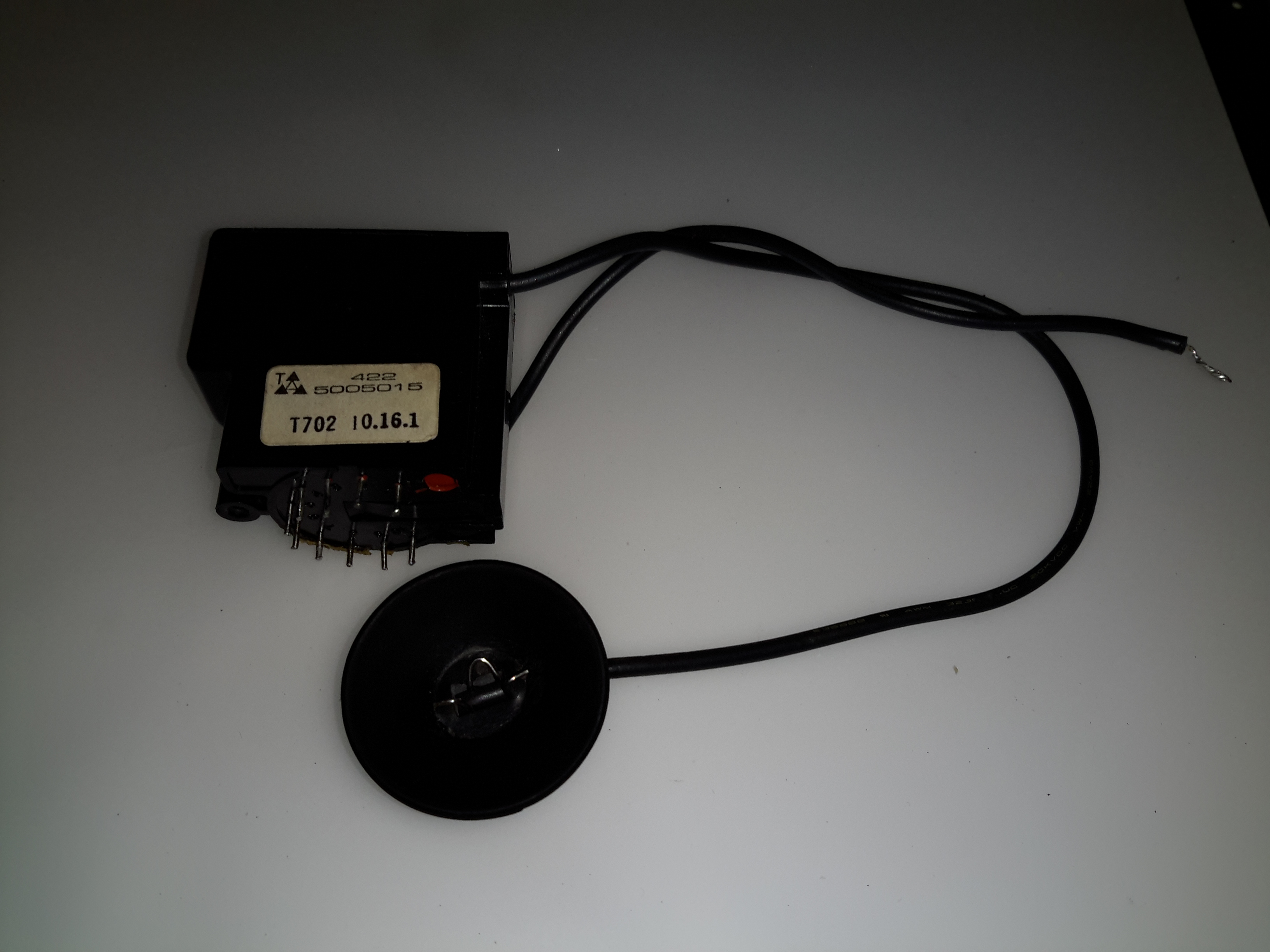
Here’s a small flyback / Line Output Transformer from a portable colour TV set. Usually these transformers are vacuum potted in hard epoxy resin & are impossible to disassemble without anything short of explosives. (There are chemical means of digesting cured epoxies, but none of them are pleasant). This one however, was potted in silicone, so with some digging, the structure of the transformer can be revealed.
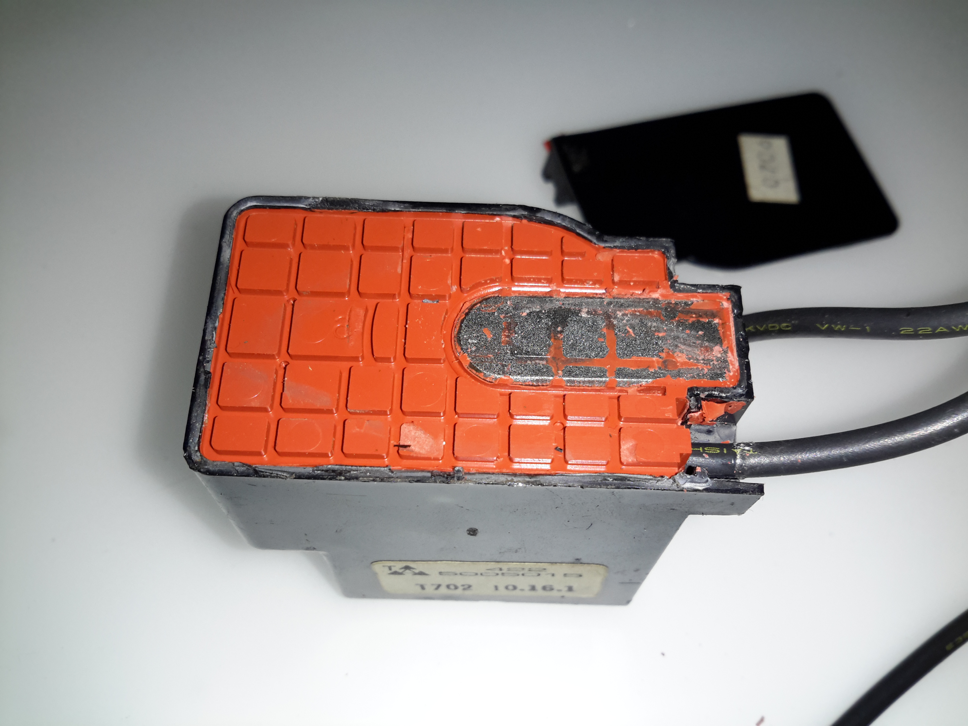
Cap Removed
The cap was glued on to the casing, but this popped off easily. The top of the core is visible in the silicone potting material.
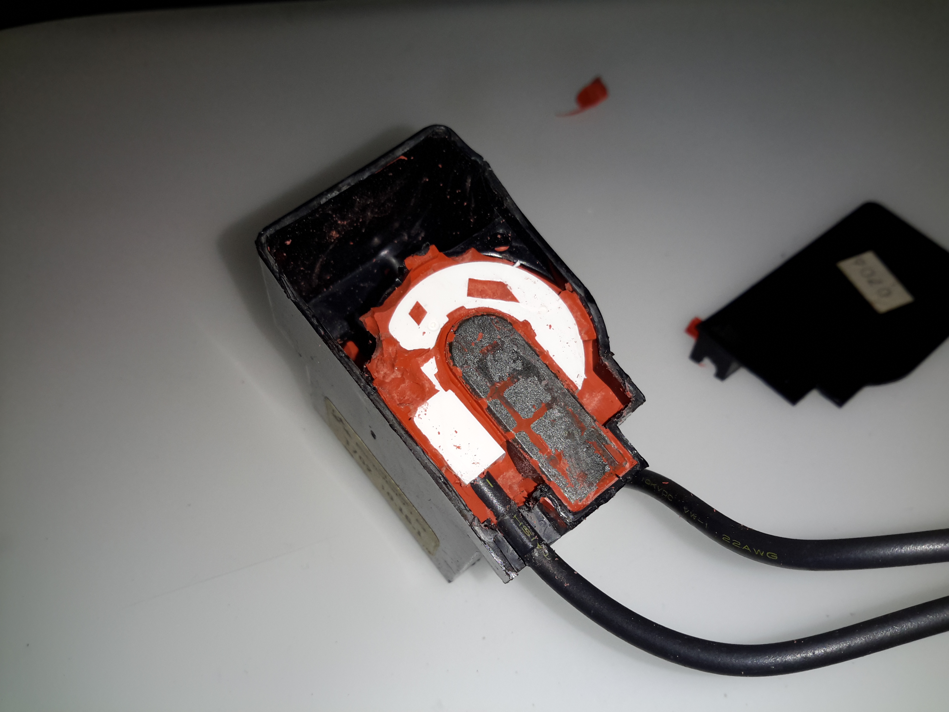
The Digging Starts
A small screwdriver was used to remove the potting material, while trying not to damage the winding bobbin & core too badly. The bulge in the casing that I originally thought might house a voltage multiplier turns out to be totally empty. The white plastic bobbin is becoming visible around the core.
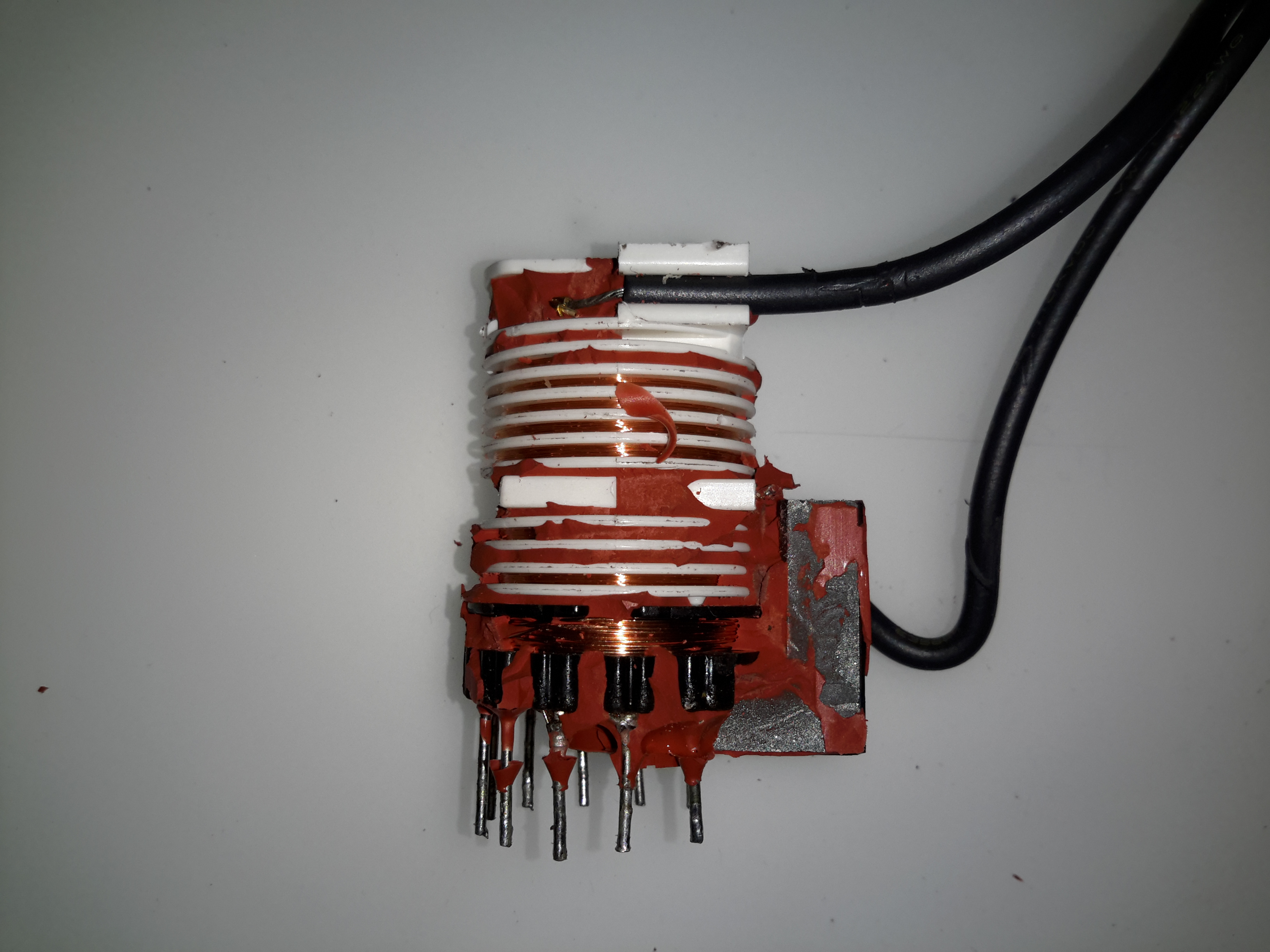
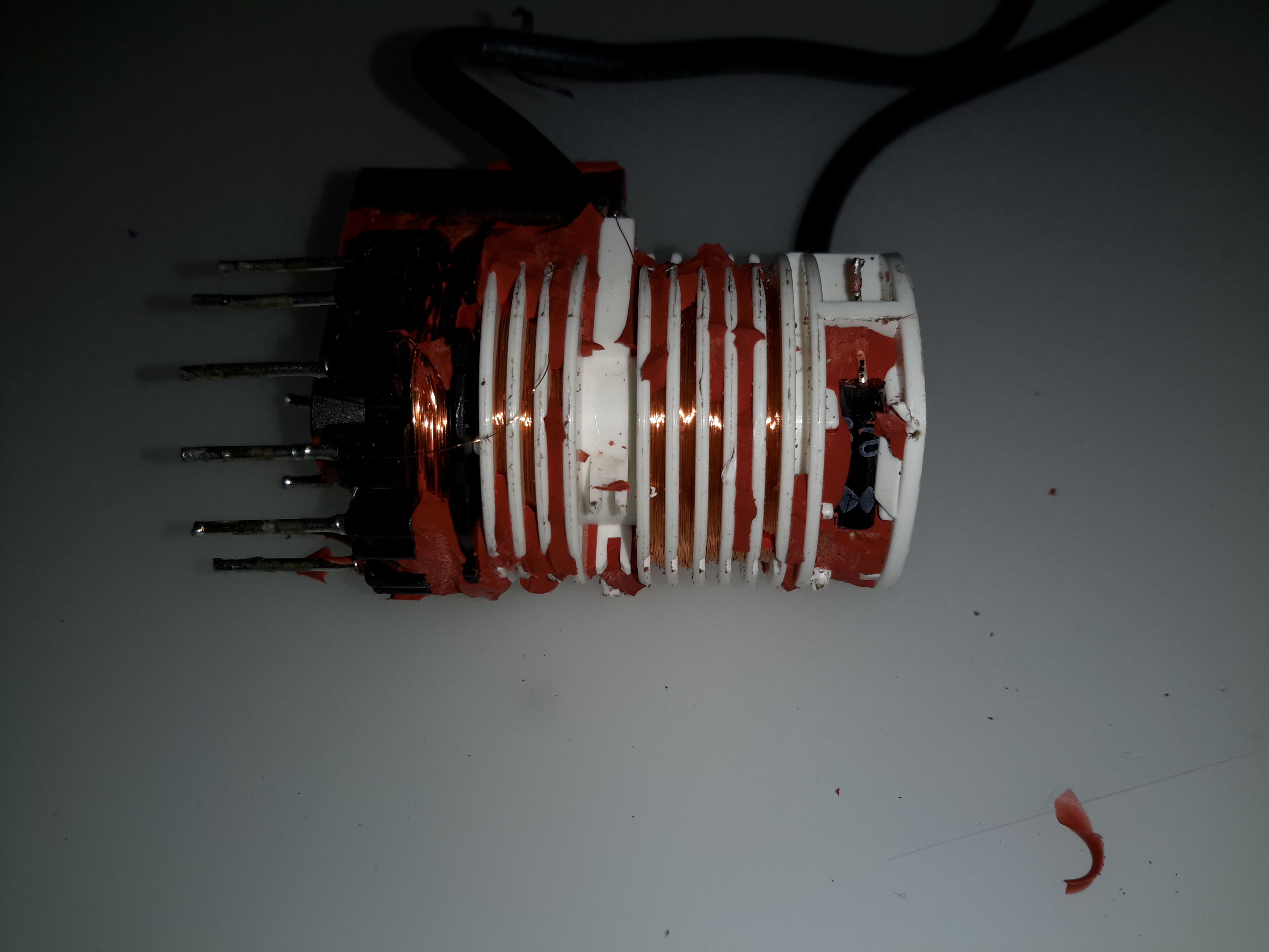
Bobbin
After some more digging & a lot of mess later, the entire transformer is revealed. The primary & auxiliary secondaries are visible at the bottom of the transformer, next to the pins. These transformers have multiple windings, as they’re used not only for supplying the final anode voltage of several Kilovolts to the CRT, but many of the other associated voltages, for the heater, grids, focus electrodes, etc. These lower voltage windings are on the same part of the core as the primary.
Above those is the main high voltage secondary winding, which looks to be wound with #38-#40AWG wire (about the thinnest available, at 0.07mm diameter. This is wound in many sections of of a few hundred turns each to increase the insulation resistance to the high voltage. The main anode wire emerges from the top of the bobbin.
Output Rectifier
Hidden in a recess at the top is the main HV rectifier, which on this small transformer is a single device (it’s probably not internally, most likely a series stack of diodes to get the PIV rating required).
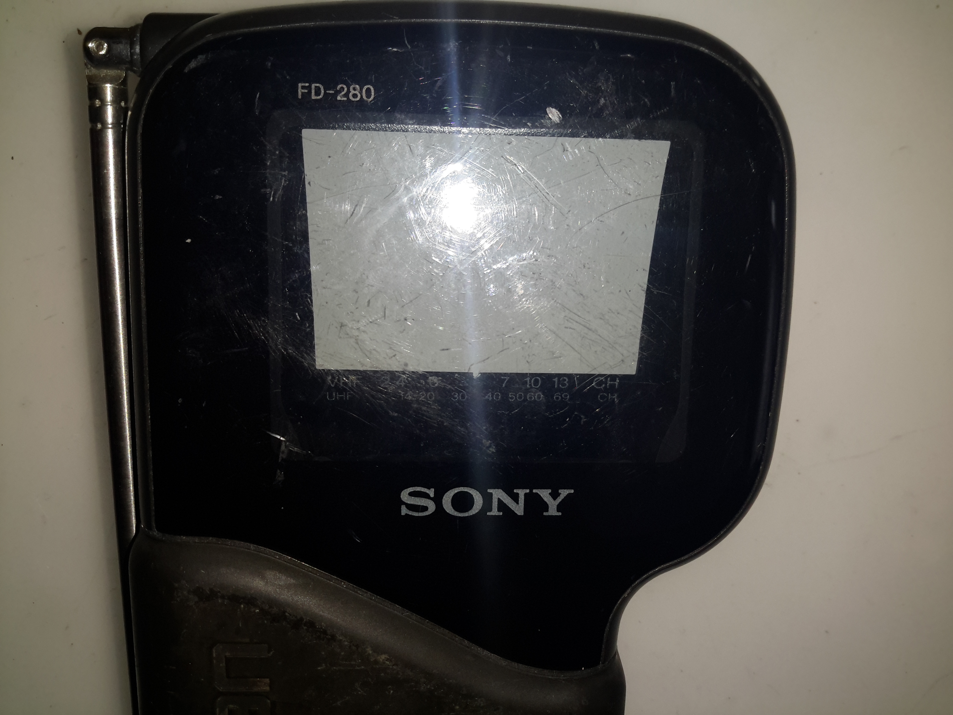
Here’s another Sony Flat CRT TV, the FD0280. This one was apparently the last to use CRT technology, later devices were LCD based. This one certainly doesn’t feel as well made as the last one, with no metal parts at all in the frame, just moulded plastic.
CRT Screen
Being a later model, this one has a much larger screen.
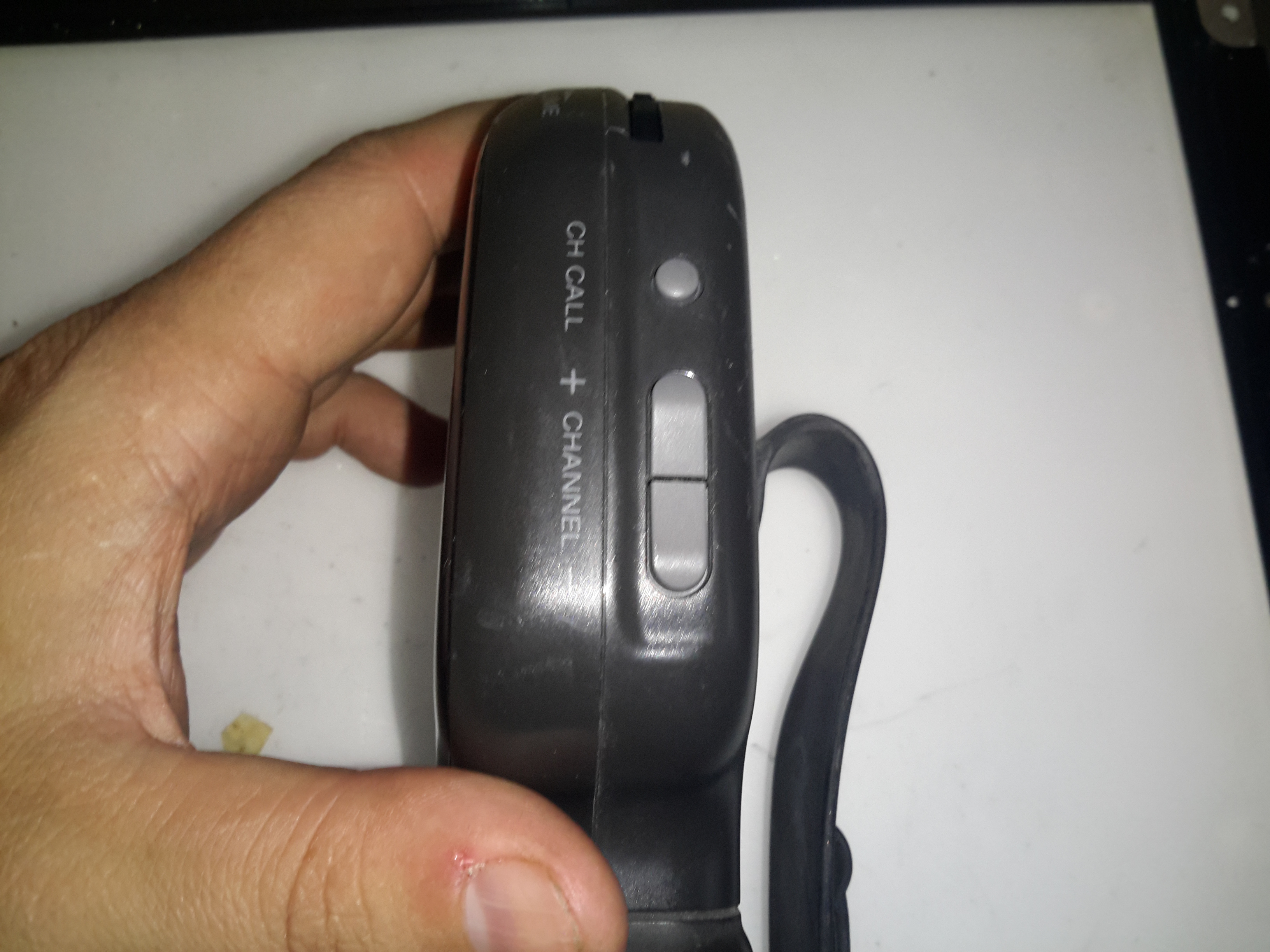
Autotuning
Instead of the manual tuner of the last Watchman, this one has automatic tuning control, to find the local stations.
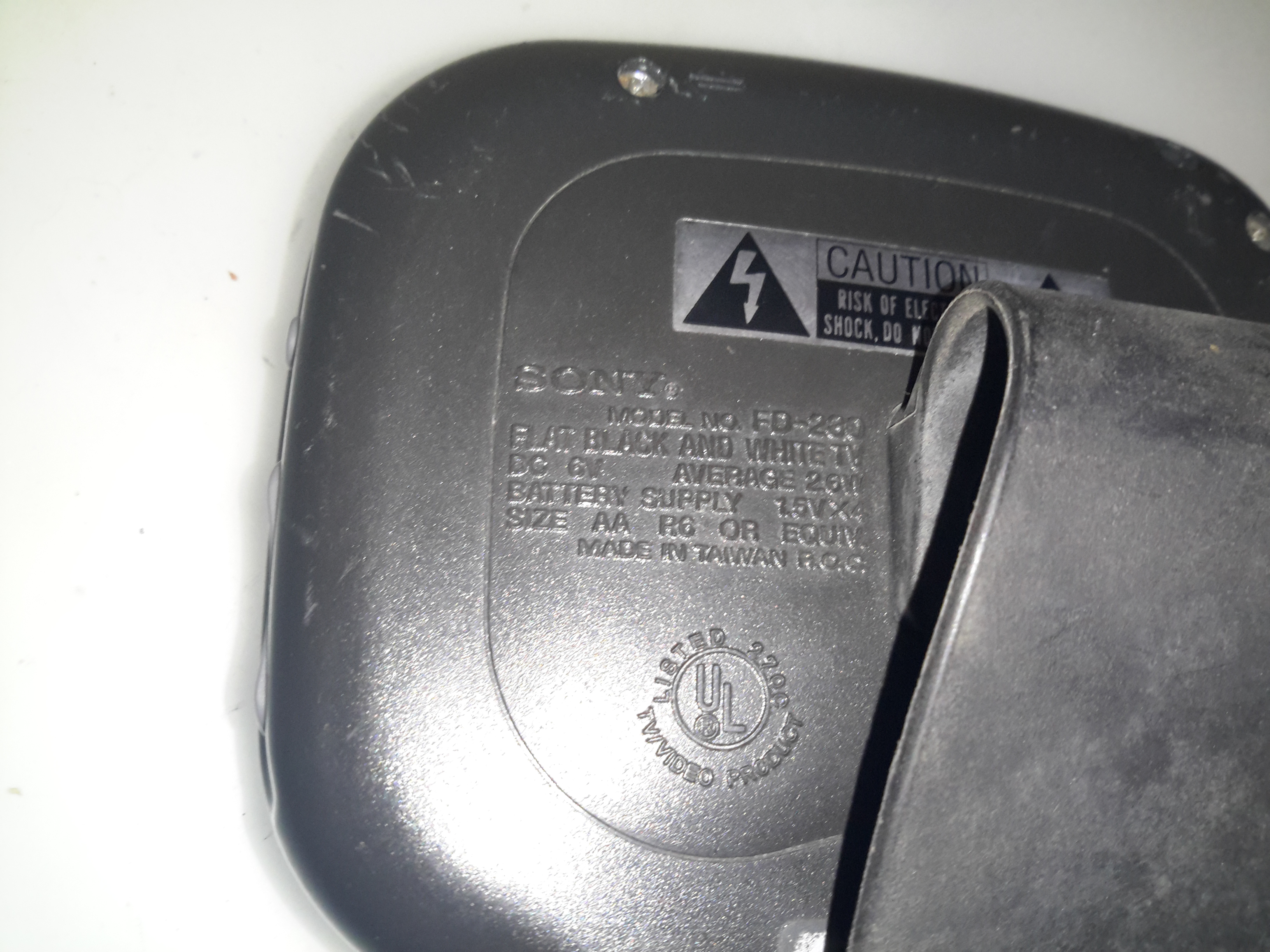
Spec Label
The spec puts the power consumption a little higher than the older TV, this isn’t surprising as the CRT screen is bigger & will require higher voltages on the electrodes.
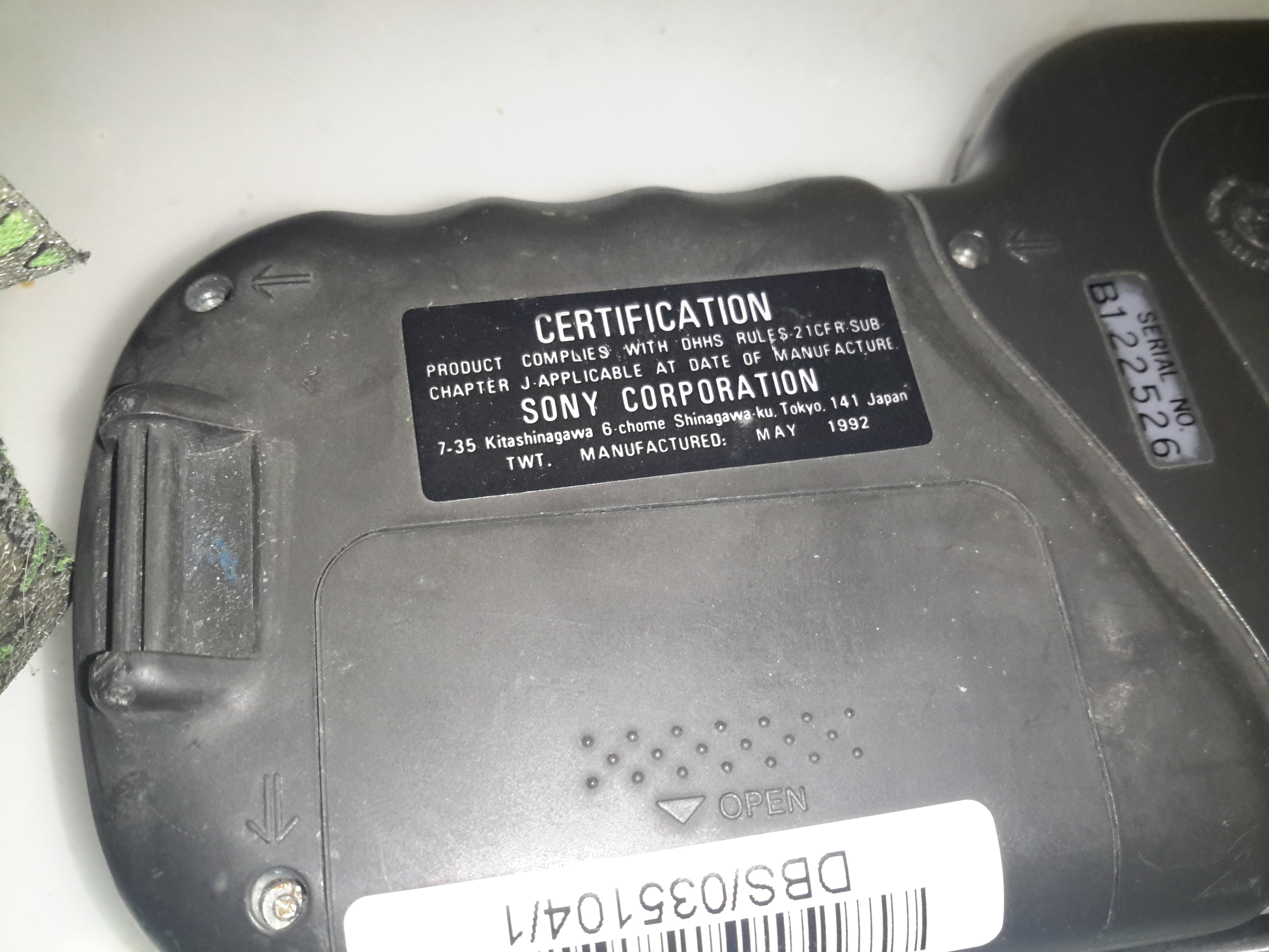
Certification Label
The certification label dates this model to May 1992.
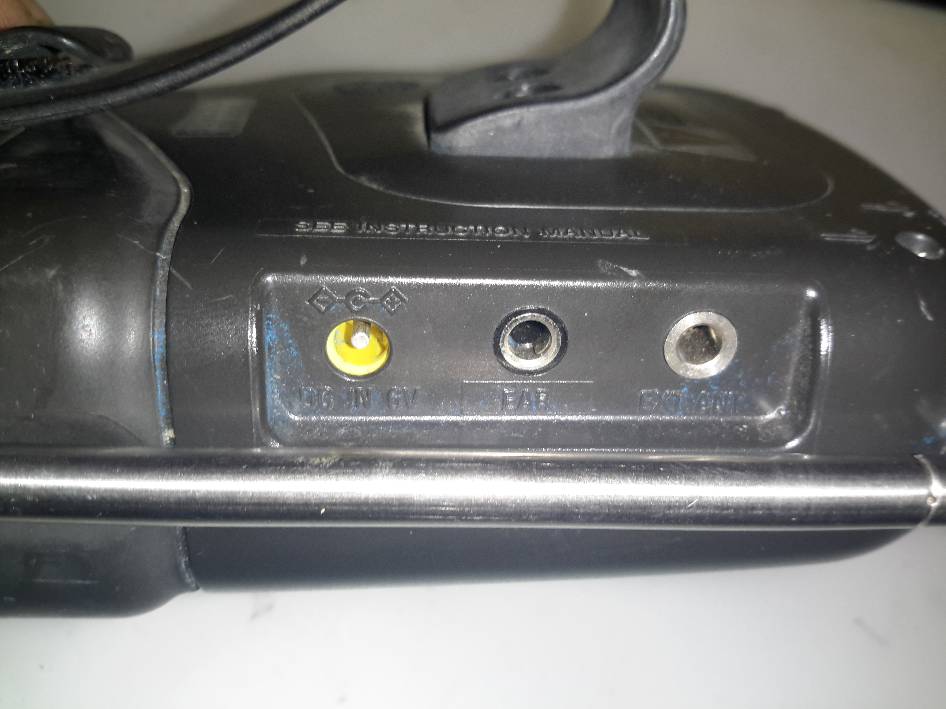
External Inputs
Still not much in the way of inputs on this TV. There’s an external power input, external antenna input & a headphone jack. No composite from the factory. (Hack incoming ;)).
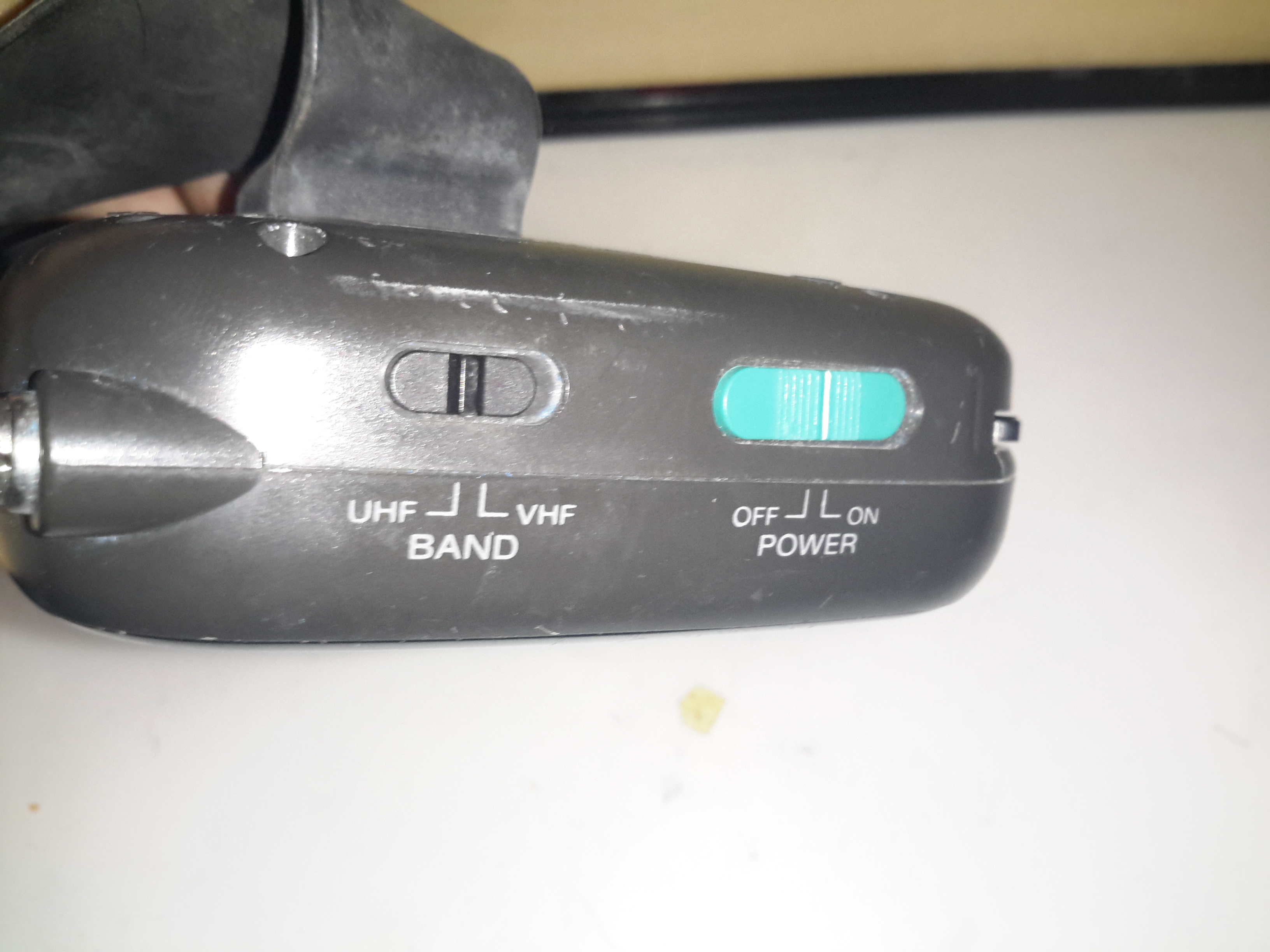
Power / Band
The UHF/VHF & power switches are on the top of this model.
Back Cover Removed
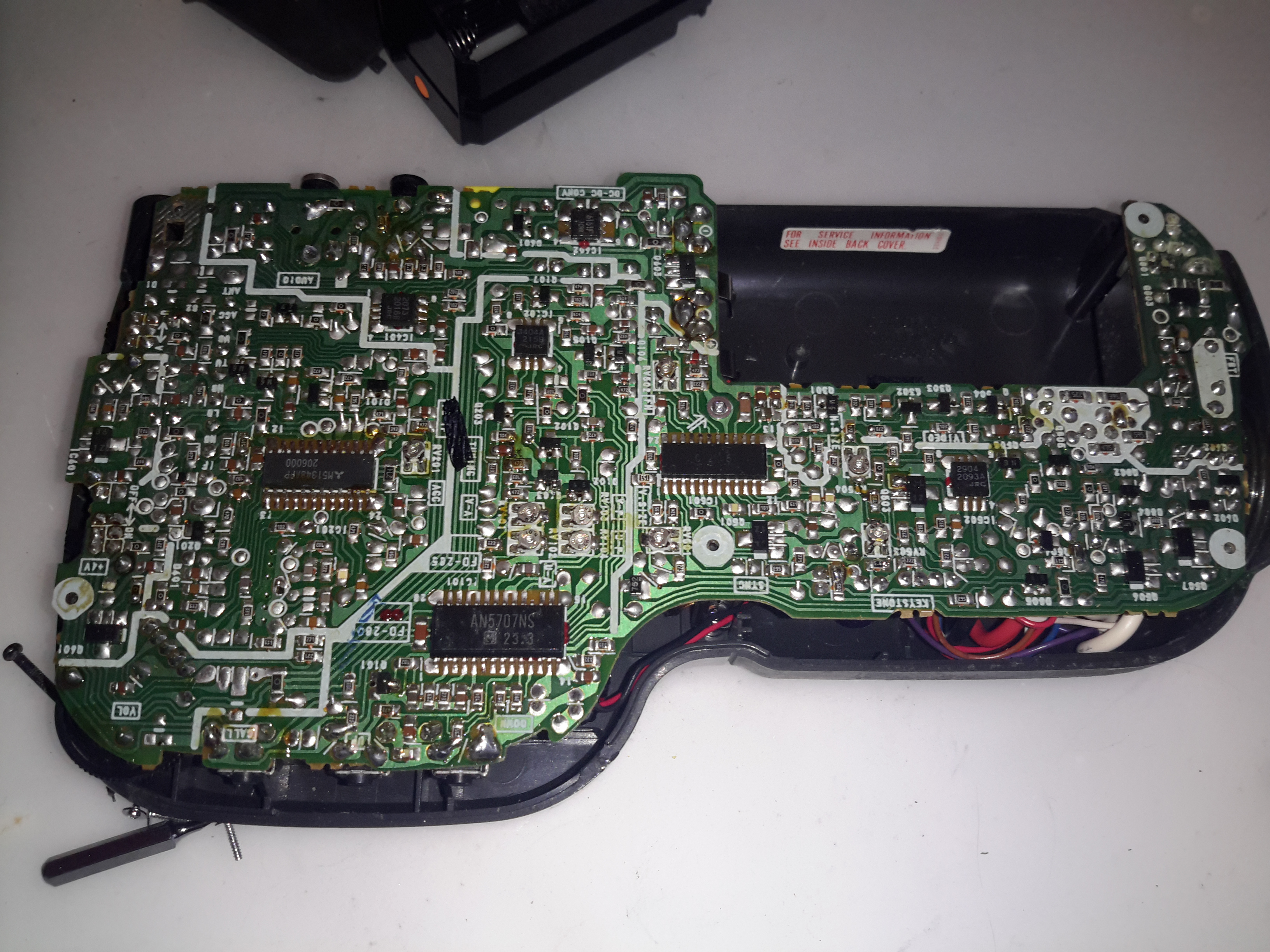
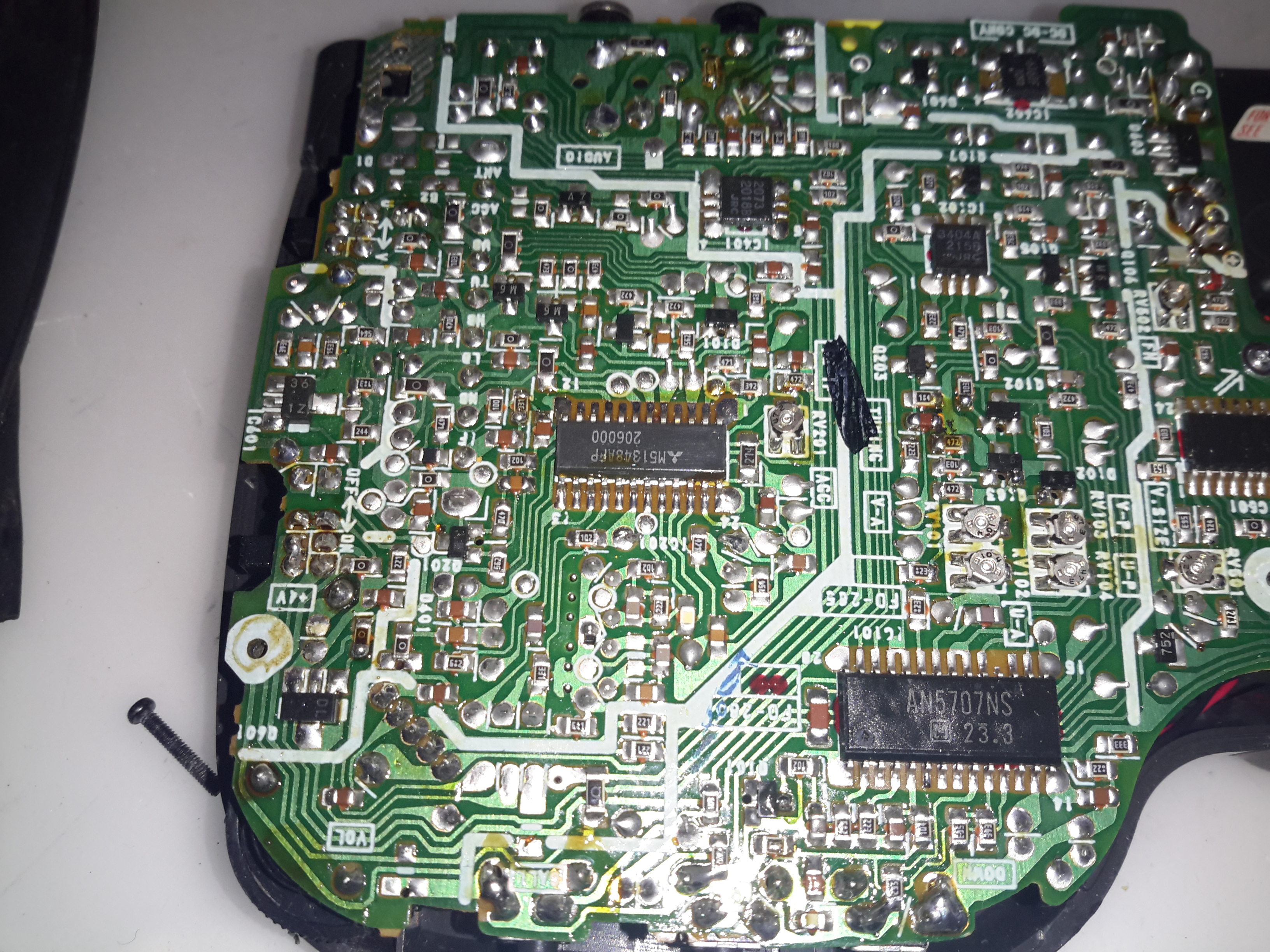
Removing some very tiny screws allows the back to be removed. There’s significant difference in this model to the last, more of the electronics are integrated into ICs, nearly everything is SMD.
RF Section
There’s the usual RF tuner section & IF, in this case the VIF/SIF is a Mitsubishi M51348AFP.
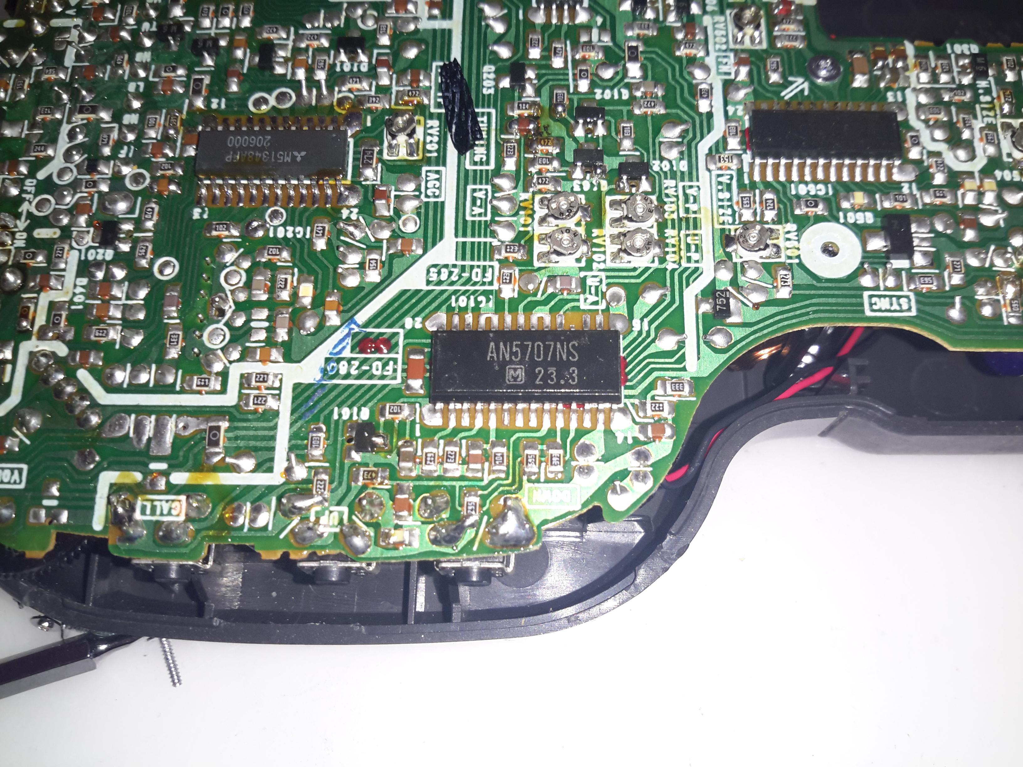
Tuner Controller
The digital control of the tuner is perfomed by this Panasonic AN5707NS.
Deflection / Sync
The deflection & sync functions appear to be controlled by a single Sony branded custom IC, the CX20157. Similar to many other custom Sony ICs, a datasheet for this wasn’t forthcoming.
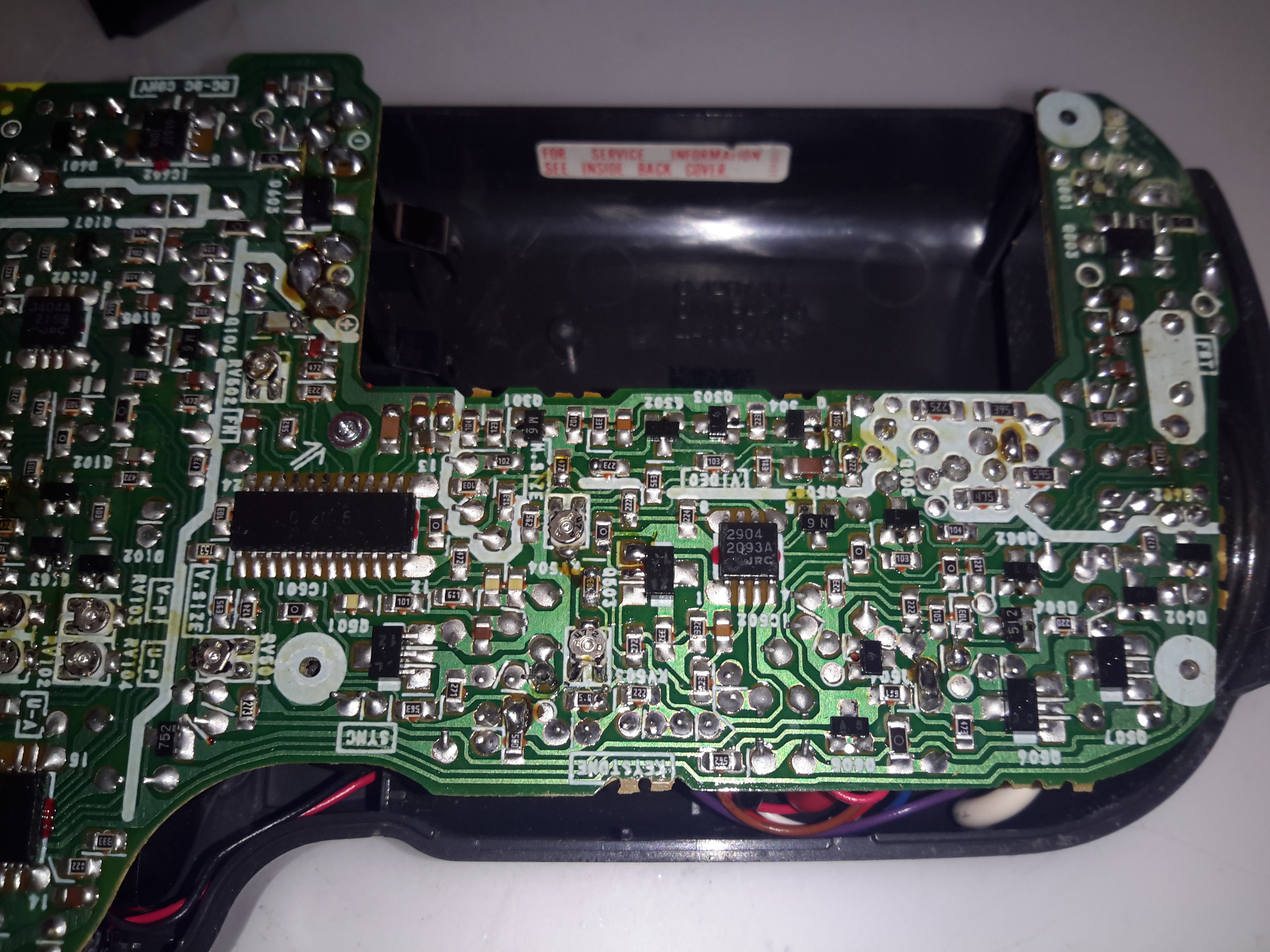
PCB Top
There’s very little on the top side of the board, the RF section is on the left, there’s a DC-DC converter bottom centre next to the battery contacts. This DC-DC converter has a very unusual inductor, completely encased in a metal can. This is probably done to prevent the magnetic field from interfering with the CRT.
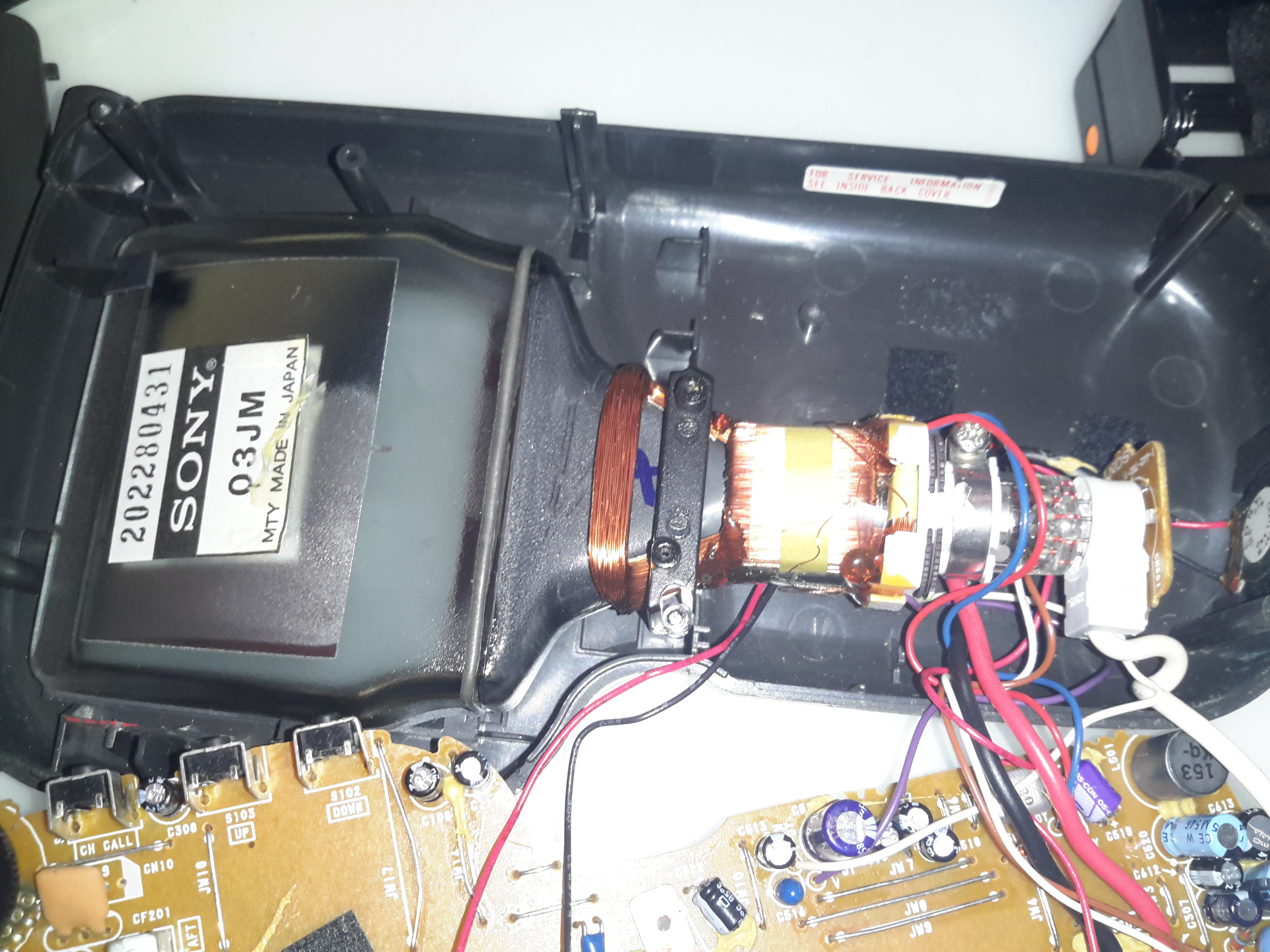
CRT
Here’s the CRT itself, the Sony 03-JM. The back of this CRT is uncoated at the bottom, the tuning scale was taped to the back so it lined up with the tuning bar displayed on the screen.
Electronics
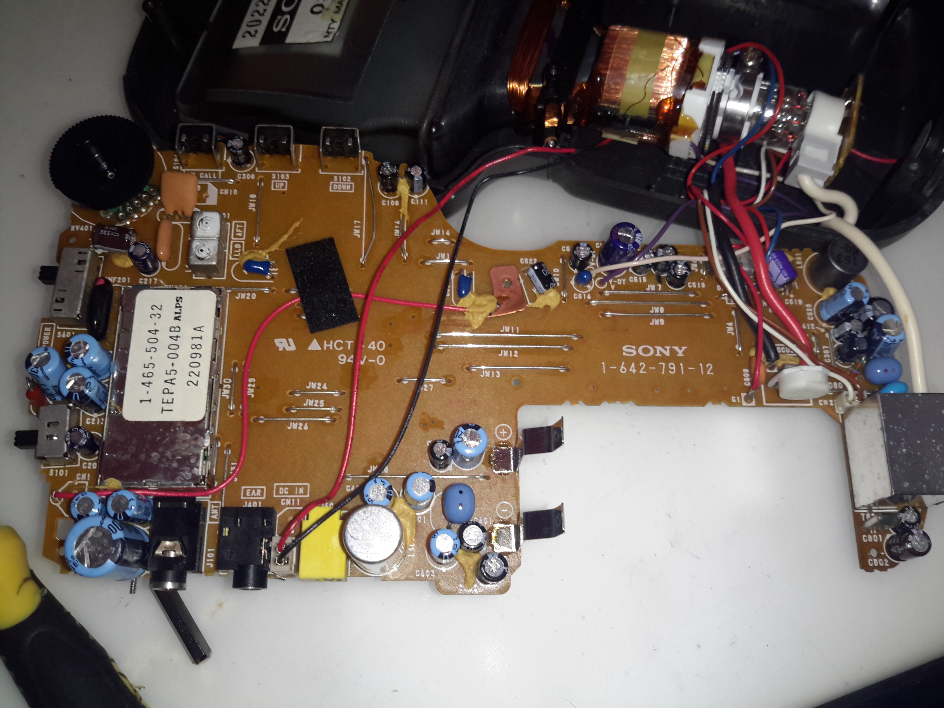
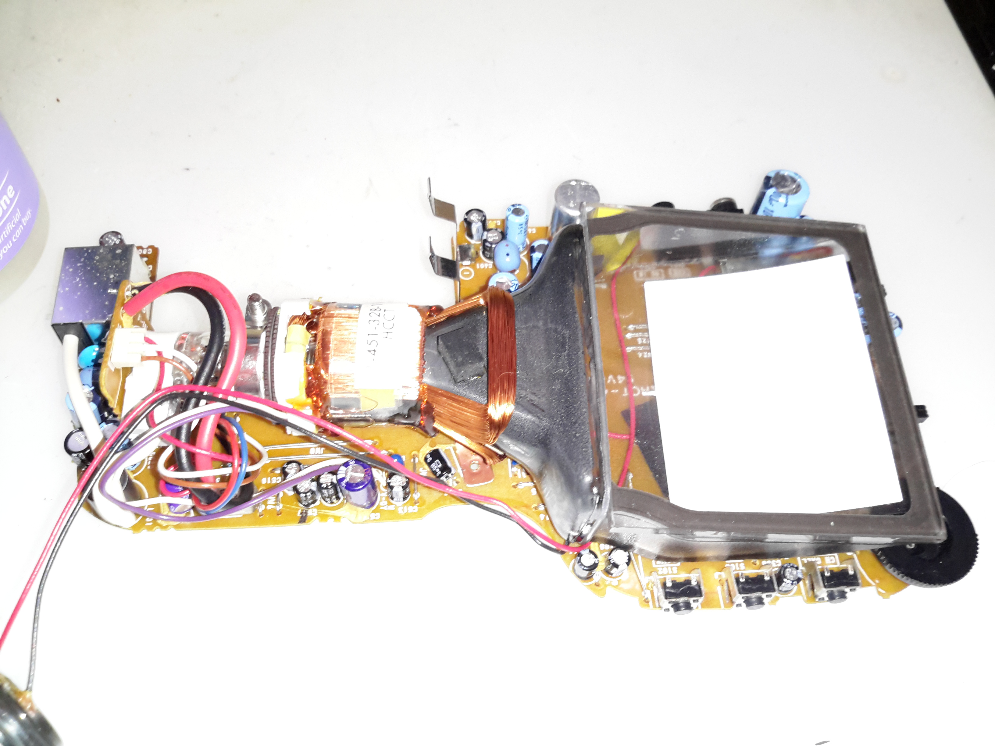
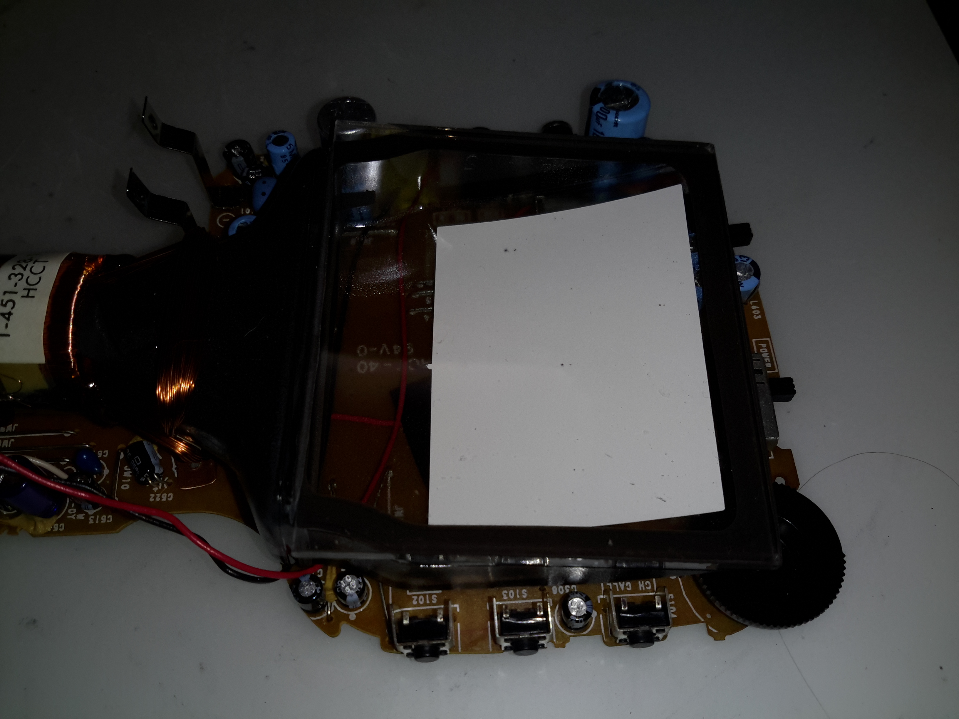
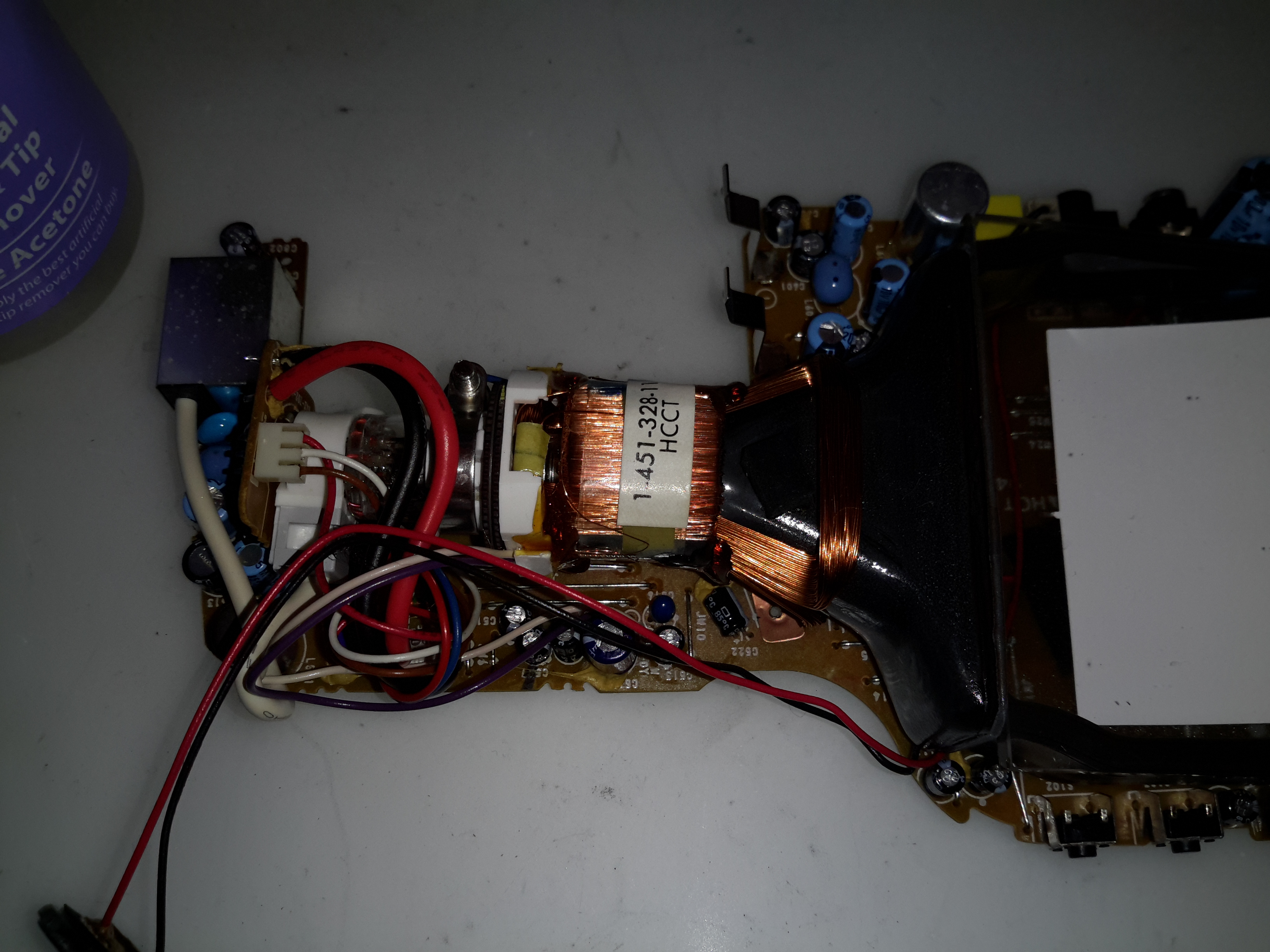
Here’s the electronics completely removed from the shell. There’s much more integration in this model, everything is on a single PCB.
Phosphor Screen
The curve in the phosphor screen can clearly be seen here. This CRT seems to have been cost-reduced as well, with the rough edges on the glass components having been left unfinished.
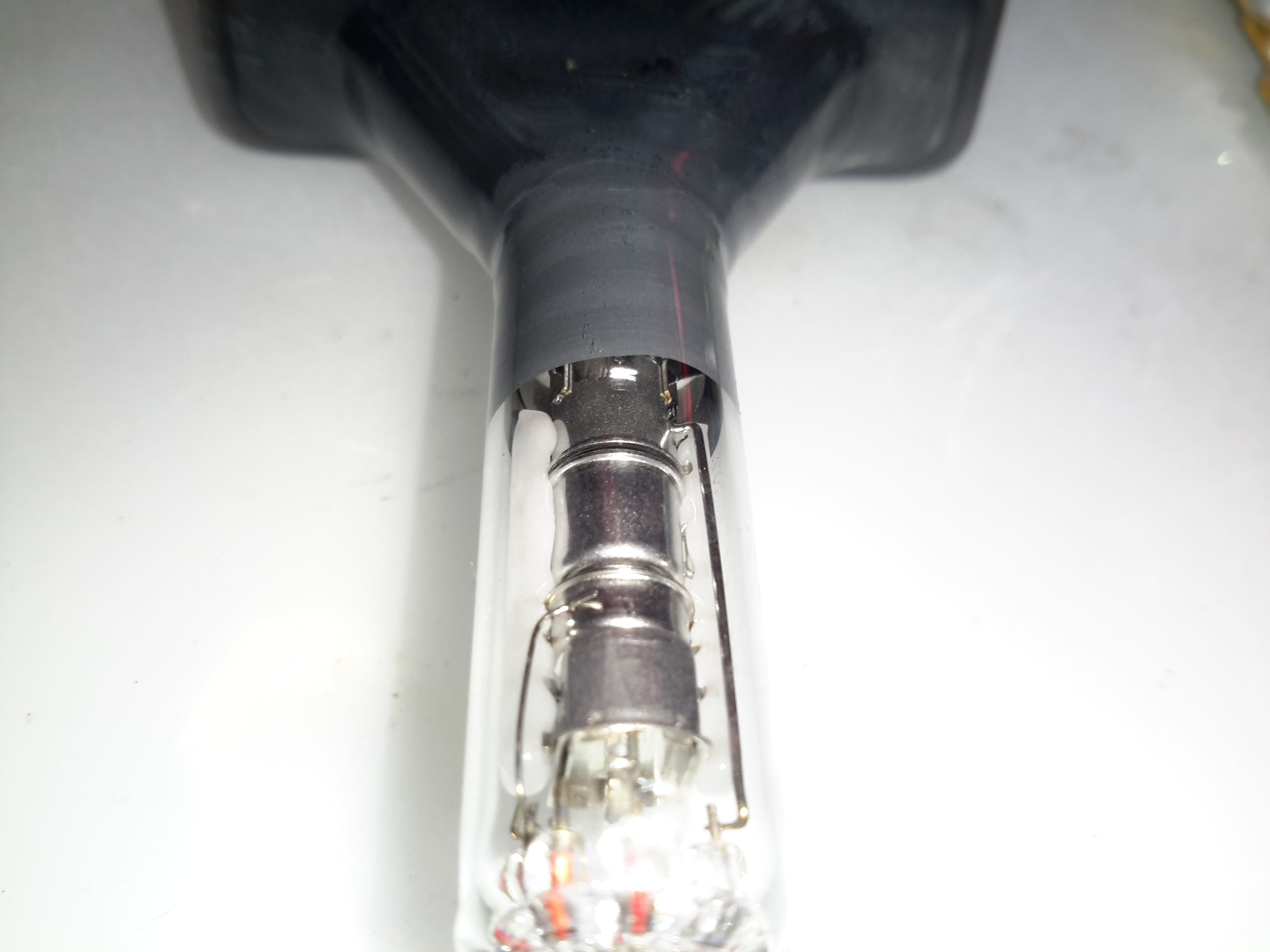
Electron Gun
Here’s the electron gun end of the tube. There isn’t a separate final anode connection to the bell of the tube unlike the previous model. Instead the final anode voltage is on a pin of the electron gun itself. This keeps all the wiring to the tube at one end & shortens the high voltage cable.
Electron Gun
Here’s the gun in the neck of the tube. Again this is pretty much standard fare for CRT guns. It’s more similar to a viewfinder tube in that the anode connection is running from the pins at the back. (It’s the line running up the right side of the tube). I’m guessing the anode voltage is pretty low for this to work without the HV flashing over, probably in the 2-4kV range.
SG-HM2 is a modular He-Ne laser power supply based on IC-HI1 with some minor enhancements. The first version is for laser tubes up to approximately 1 mW (2 mW with trivial modifications) but it should be straightforward to go to 5 mW or even higher power tubes by replacing the SG-HM2 HV Module (HVM2-1) with one with a higher voltage and current rating, along with a higher power MOSFET and minor component value changes to the Control Module (suggestions below). I have added an adjustment for tube current, a current limiting resistor and Zener to protect against output short circuits, an enable input (ground to turn on), a bleeder resistor to virtually eliminate the shock hazard after the power supply is turned off, and power and status LEDs.
Get the schematic for SG-HM2 (1 mW version) in PDF format: [download id=”5610″]
Modifying SG-HM2 for Higher Power He-Ne Laser Tubes
The following are guidelines for modifying SG-HM2 to drive various power He-Ne lasers. The PCB layout below with two versions of the HV Module should accommodate He-Ne laser tubes up to 10 mW. All assume input of around 12 V though a higher power system can generally run lower power lasers at reduced input voltage. If operation at rated power on another input voltage is desired, the number of turns on the inverter transformer can be adjusted accordingly. As noted above, the 1 mW HV Module (HVM2-1) should run tubes up to about 2 mW, though increasing the µF values of some of the HV capacitors may be desirable to reduce ripple at the higher tube current. Minor changes may also be needed in the components on the SG-HM2 Control Module including using a higher power MOSFET for Q1 and reducing the values of R7 and/or R8 for the higher tube current. Or, just populate the Control Module with Q1 being an IRF644, R7 being 150 ohms, and R8 being 750 ohms for compatibility with all the HV modules. For that matter, the HVM2-5 PCB HV Module should be usable with lower power lasers.
   Laser Power       1 mW         2 mW         5 mW         10 mW
-----------------------------------------------------------------------
   Voltage           1200 V       1500 V       2300 V       3500 V
   Current           2-4mA        3-5mA        5-7mA        5-7mA

 SG-HM2 HV Module:

   PCB Version       HVM2-1       HVM2-1       HVM2-5       HVM2-5

   T101
    Core (DxH)       18x11 mm     18x11 mm     26x16 mm     26/16 mm
    Primary          9T,#28       9T,#28       9T,#26       9T,#26
    Secondary        450T,#40     450T,#40     600T,#40     900T,#40
     Res. (Est)      60 ohms      60 ohms      (90 ohms)    (120 ohms)

   D101-106          2kV          2kV          3kV          5kV

   C101-104          1nF,3kV      2nF,3kV      2nF,6kV      2nF,6kV
   C105              47pF,3kV     47pF,3kV     100pF,6kV    100pF,6kV
   C106              3nF,10kV     5nF,10kV     6nF,15kV     6nF,15kV

   R102              10K,1/2W     10K,1/2W     10K,1W       10K,1W
   R103              200M,10kV    200M,10kV    200M,15kV    200M,15kV
   R106-107 (total)  10M          10M          15M          20M

 SG-HM2 Control Module:

   Q1              IRF630       IRF630       IRF640       IRF644
   R7              300          250          150          150
   R8              500          250          100          100
SG-HM2 Inverter Transformer
The inverter transformer for HVM2-1 is wound on a ferrite pot core with a small air-gap (about 0.005″). It is 18 mm in diameter by 11 mm high. While specified to use a 9 turn primary and 450 turn secondary, these values can be adjusted somewhat to handle various input and output requirements. Don’t go much lower on the primary as this may result in core saturation. The 9/450 transformer should be fine for 1 to 2 mW He-Ne laser tubes running on 8 to 15v DC input. With 9/300, it will operate on about 12 to 20v DC. Increasing the number of secondary turns (e.g., 9/600) may result in operation on a slightly lower input voltage, but probably not by much. The 9/450 transformer may even run He-Ne laser tubes larger than 2 mW but I haven’t yet tested this since I haven’t built a prototype of HVM2-5 as yet.
It doesn’t matter very much whether the primary (P) is wound first or the secondary (S) is wound first though the former appears to work slightly better, running the tube at about 8v DC input instead of 9v DC input for the same 9/450 transformer. P over S is slightly easier to wind since the primary doesn’t get in the way and increase the lumpiness of the secondary layers. However, with S over P, insulation is somewhat less critical since the HV lead is out away from anything else. With the P over S, additional insulation is needed between them. Also, since the primary coil is larger diameter, it will have more resistance and there will be greater inter-winding capacitance (though probably not significant). The secondary should be constructed as multiple layers of about 50 or 60 turns each, with insulating tape between layers. Each should be wound in as close to a single layer as possible with alternating layers staggered to prevent arc-over. This doesn’t have to be perfect but try to go gradually from one side to the other to keep wires at high relative potential away from each other. Make sure the HV output leads (particularly the one away from the dot) are well insulated as they exit the transformer. And, as noted, if the primary is over the secondary, there must be high voltage insulation between them. The peak output voltage when the MOSFET turns off (the flyback pulse) may be more than 5 times higher than what would be expected from the DC input voltage and the turns-ratio alone – several kV and this *will* try to find a path to ground! There are more detailed transformer construction instructions in the next section.
Note that this transformer is slightly larger physically than the one from IC-HI1. This is for two reasons: (1) It is easier to wind with more space and a larger wire size for the secondary, and (2) continuous operation should be possible with 2 mW laser tubes, which might have been marginal with the original transformer used in IC-HI1. A by-product of the larger core is that its 9 turn primary should be roughly equivalent to the 12 turn primary of the smaller core in terms of inductance and core saturation limitations.
Interestingly, a similar transformer found in a different commercial power supply, had no insulating tape anywhere. It would appear that with very precise machine-wound HV secondary, done first, the voltage is distributed so uniformly that this is unnecessary.
I’ve now built and tested several transformers in IC-HI1, removing the original transformer and installing socket pins so either the original or an adapter board can be plugged in. This setup is then equivalent to SG-HM2 with the HVM2-1 HV Module. The minimum input voltage values that follow are when driving a 0.5 mW He-Ne laser tube:
           Turns        Pot Core   Vin (VDC)
   ID   P/S    Order    (DxH mm)   Min  Max           Comments
 ------------------------------------------------------------------------------
   1* 12/600  S over P    14x8     7.5  15   Original IC-HI1 transformer
   2  12/350  S over P    18x11    14   22   First prototype, described above
   3   9/350  S over P    18x11    11   18   #2 with 3 P T added out-of-phase
   4   9/425  P over S    18x11     9   16
   5   9/450  P over S    18x11     9   16
   6   9/450  S over P    18x11     8   15
   7  12/500  P over S    26x16     8   15
*The number of turns on the original (#1) is not really known exactly and may be lower or higher by up to 25 percent based on the measured secondary resistance (45 ohms) and estimated wire size (somewhere between #38 and #40. (Even with the larger wire, the amount of bobbin area taken up by the wire is less than 50 percent so it should fit even with many layers of insulating tape. The transformer is Epoxy impregnated and likely to be impossible to disassemble into any form that can be analyzed!)
All of these transformers will drive He-Ne laser tubes of up to at least 2.5mW using the equivalent of the HVM2-1 HV Module which is part of IC-HI1. Even with the 2.5mW tube, the minimum operating voltage was only about 0.5v higher than for the 0.5mW tube. There is a good chance they would drive even larger He-Ne laser tubes (though possibly at a slightly higher input voltage) but I don’t dare try using the existing HV circuitry as it might not survive for long. I suspect that transformers #4, #5, and #6 would run on an input voltage of less than 8v DC but the salvaged cores I am using have a larger air-gap than might be optimal and I don’t have anything to reduce it without heavy losses. They attempt to start the tube at around 6v DC but are unable to maintain it and flicker rapidly. (#2 and #3, which use the same style core, would also benefit somewhat.) Operation using #1 and #5 is virtually identical, with the original running at perhaps 0.5v DC less input. I expect they would be even more identical if the air-gap on #5 were smaller, and #6 with its smaller air-gap does indeed run at the lower input voltage. I haven’t actually confirmed that anything blows up above the maximum voltages listed above, which were arbitrarily chosen. But I am guessing that bad things might happen at some point. 🙂
I have also constructed a transformer which will need to be used with HVM2-5: 12/1200, P over S, on a 30×19 pot core. I will also construct a 9/900. S over P, on a 30×19 pot core (or on a 26×16 if I can find one). Testing of these will have to await an HVM2-5 prototype.
SG-HM2 Transformer Construction
Here are details on construction of the inverter transformer for SG-HM2. With all parts and tools on hand, it takes about an hour start to finish. Only a small portion of this time is in the actual winding (at least if a coil winding machine is used). Most of the time is spent in adding the insulation tape and terminating the leads. After constructing a few of these, it does go quicker. 🙂
Step-by-step instructions are provided for the HVM2-1 transformer. The changes needed for HVM2-5 are summarized at the end of this section. Some sort of coil winding machine is almost essential as #40 wire is extremely thin and easy to break. (Anything larger than #40 will not fit on the bobbin.) It doesn’t have to be fancy. Mine is probably 50 years old of the type that is (used to be?) advertised in the back of electronics magazines. However, a couple of spindles – one that is fixed or free to rotate for the wire supply and the other which can be turned for the coil being wound – are really all that are needed. Don’t use any sort of powered approach though (unless you have a *real* professional coil winder!) as it is all too easy to break the wire if there is no tactile feedback to detect snags.
Parts required for T101 of HVM2-1:
18×11 mm (1811) ferrite pot core with a small air-gap (no more than 0.005″) or no air-gap, and a single section bobbin. These are available from several manufacturers but surplus or salvaged cores may be easier to obtain. Radio Shack used to have a “ferrite kit” which included a variety of sizes of cores (only 1 each though so you’d have to buy two kits and there were no bobbins!). I doubt the kit still exists though.
Approximately 1.5 feet of #28 magnet wire for the primary (9 turns wound first) and approximately 60 feet of #40 magnet wire for the secondary (450 turns wound on top of the primary). I found both these size wire in various solenoids and relays I’ve discombobulated. 🙂 Wire sizes aren’t critical but these are known to fit and the #40 can be handled with a reasonable chance of not breaking.
Sleeving to protect the primary wires where they leave transformer. I used approximately 2″ of insulation (each lead) from the individual wires in some 25 pair phone cable.
Wirewrap wire or other thin insulated wire to terminate the secondary wires where they leave the transformer.
Insulating tape. 1 mil Mylar or similar is desirable. However, I’ve found that thin clear (non-reinforced) packing tape does an adequate job, though it probably doesn’t have as much dielectric strength as real insulating tape so additional layers are required. It will also likely not stand up to overheating too well. Electrical tape is way too thick and would prevent enough turns from fitting.
A piece of Perf. board with holes on 0.1″ centers, 0.8″x0.8″. There should be 7 rows of holes each way so that one hole lines up in the center.
A Nylon 4-40 screw and nut to fasten the transformer to the board.
Four (4) machined-type IC socket pins or something similar to use as terminals.
Wind the primary:
Slip a piece of sleeving over the start of the primary wire and position the sleeving so it extends about 1/2 turn inside the bobbin on the left side.
Wrap exactly 9 turns of this wire clockwise around the bobbin, left to right. The wires should enter and exit on the same angular position (slot) of the bobbin on opposite sides.
Slip another piece of sleeving over the wire end exiting the bobbin so that it too is about 1/2 turn inside the bobbin.
Wrap 1.5 to 2 turns of tape tightly over the primary winding to secure and insulate it.
Wind the secondary:
Strip 1/8″ or so from the end of a 2″ piece of wire-wrap wire and solder the start of the wire for the secondary winding to it. Make sure the insulation on the fine magnet wire has been removed – usually just heating it while soldering will do this. Leave an inch or so of the magnet wire extending from the connection so that continuity can be confirmed with a multimeter, then snip it off. Install this in the opposite slot of the bobbin also on the left side with about 1/4″ of insulation inside the bobbin against the side and separated from the primary. Leave a little slack in the fine secondary wire so that slight motion won’t break it. Add a small piece of tape to protect and insulate this connection.
Using your coil winding machine (you do have one, correct?), build up the secondary in layers of about 50 to 75 turns in a counter-clockwise direction (bobbin being rotated clockwise). A single layer of wire won’t fit in the 1/8″ or so available (in the 18×11 mm core bobbin) so there will have to be some overlap. But, do this several times across the layer so that any given wire won’t be next to one with a much different voltage. In other words, wind a few turns and back up so that there will in essence be multiple sub-windings of 5 or 10 turns, repeated several times across the layer. Keep the wire at least 1/32″ away from either edge of the bobbin.
After each full layer or wire, add just over 1 layer of insulating tape making sure it covers the entire width of the bobbin. There should be just enough overlap to assure there is at least 1 layer of insulation but not much more as excessive tape will end up taking up too much space.The entire 450 turn winding will then require 6 to 9 full layers. Add another layer of insulating tape over the last winding layer leaving the wire end exposed.
Terminate the end of the secondary winding with another piece of thin wire by soldering as above. Confirm continuity with a multimeter. For the 450 turn secondary, the resistance should be about 60 ohms. Add a piece of thicker sleeving over this at the HV end if space is available. Else, use some bits of tape to insulate the wirewrap wire lead from the core and exposed inner layers that it may come near as it exits out the side of the bobbin. Add another layer of tape to secure the lead in place.
Add several more layers of insulating tape to complete the bobbin assembly.
Prepare the mounting board:
Widen the center hole to 7/64″ to accommodate a 4-40 nylon screw.
Widen the holes at the 4 corners of the board to accept the 4 IC socket pins (if used) as a press-fit or glue them in place with 5 minute Epoxy or SuperGlue.
Final assembly:
Install the ferrite pot core halves to the bobbin taking care not to crunch any of the wires. Orient it so that the primary and secondary leads are conveniently located with respect to the 4 pins, e.g., primary start: bottom left; primary end: top left, secondary start: bottom right; and primary end: top right.
Use the nylon 4-40 screw and nut to *gently* secure the transformer to the mounting board. The head of the 4-40 screw should be underneath the board. Don’t over-tighten or it may crack the core, especially if it has an air-gap in the middle.
Carefully remove the insulation from the ends of the wires. The secondary wires will still be fragile even with the wirewrap wire terminations. For the magnet wire, the easiest way to remove the insulation is to burn it off with a match or hot soldering iron and then clean with fine sandpaper.
Push the wires into their respective socket pins. (The wirewrap wires are too thin to be secure but they will make adequate contact for testing.)
Use a multimeter to confirm continuity of the primary (close to 0 ohms) and secondary (about 50 to 75 ohms).
Testing:
Install the transformer in you HV Module. Attach a He-Ne laser tube and ballast resistor.
Power up on an variable DC power supply and check for reliable starting and stable operation. Adjust the core gap if needed. A smaller gap may result in more operating power available at a given input voltage. A larger gap will result in attempts to start on a lower input voltage. Somewhere around 0.005″ is probably a good compromise.
After testing the transformer (and adjusting the core gap if needed), use some adhesive to secure the pot core sections and to protect the transformer leads. Solder the leads into the socket pins.
The final result is shown on an adapter below:
Photo of SG-HM2 HVM2-1 Transformer being Tested in IC-HI1
The instructions for winding the HVM2-5 transformer are similar except for the dimensions, wire sizes and lengths, and number of turns for the primary and secondary:
Differences in parts list for T501 of HVM2-5 compared to T101 of HVM2-1:
26×16 mm (2616) ferrite pot core with a small air-gap (no more than 0.005″) or no air-gap, and a single section bobbin.
Approximately 2.0 feet of #26 magnet wire for the primary (12 turns wound first) and approximately 75 to 120 feet of #40 magnet wire for the secondary (600 or 900 turns wound on top of the primary).
A piece of Perf. board with holes on 0.1″ centers, 1.0″x1.0″. There should be 9 rows of holes each way so that one hole lines up in the center.
A Nylon 10-32 screw and nut to fasten the transformer to the board.
Since the peak voltage on the HVM2-5 secondary may be 2 to 3 times higher than for HVM2-1, extra insulation and clearances will be required on the secondary.
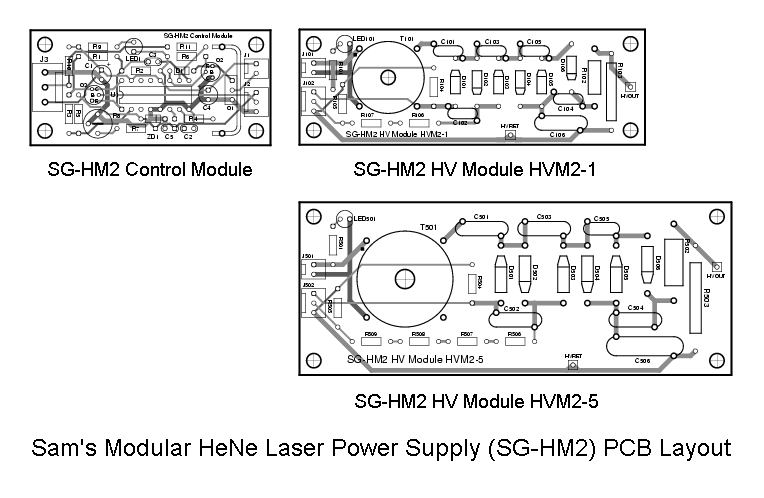
SG-HM2 Printed Circuit Board Layout
A printed circuit board layout is also available. The Control Module is 2″x1.2″. The HV Modules are 3.6″x1.2″ and 4.5″x1.8″ for the 1 mW (HVM2-1) and 5 mW (HVM2-5), respectively. The Control and HV Modules are connected by a 2 pin cable for transformer drive and a 3 pin cable for current sensing from the laser tube. The two boards can easily be merged if desired.
The layout of the 3 PCBs may be viewed as a GIF file (draft quality) as below:
Sam’s Modular He-Ne Laser Power Supply 2 PCB Layout
.
A complete PCB artwork package for SG-HM2 (all PCBs on one sheet) may be downloaded in standard (full resolution 1:1) Gerber PCB format (zipped) as [download id=”5612″]
The Gerber files include the component side copper, soldermask, and silkscreen; solder side copper and soldermask, and drill control artwork. The original printed circuit board CAD files and netlist (in Tango PCB format) are provided so that the circuit layout can be modified or imported to another system if desired. The text file ‘sghm2.doc’ (in sghm2grb.zip) describes the file contents in more detail.
Note: The netlist does NOT include wiring for the HVM2-5 HV Module. Also, part numbers on the HVM2-5 PCB actually begin with a “5” instead of a “1” since Tango PCB will not allow duplicate part numbers on the same layout.
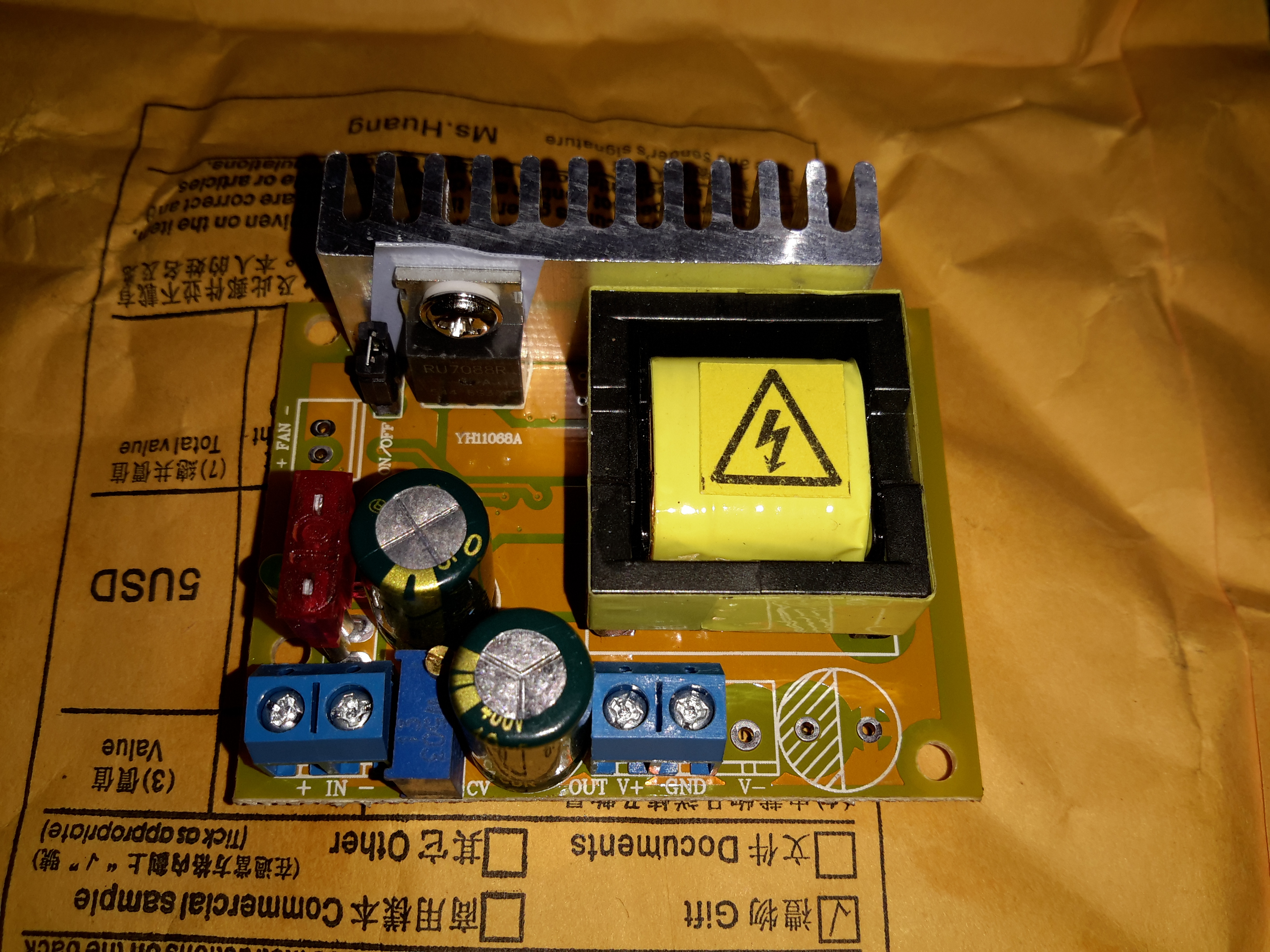
Going through eBay recently looking for parts for a couple of CRT-based projects, I came across these DC-DC converters.
Apparently rated from 45-390v DC output at 200mA, these should be ideal for driving some of the electrodes (focus, screen, grid) in a CRT.
Above is the top of the board, input voltage header on the left, output voltage adjust in the centre & output voltage header on the right.
This module has a mini-automotive fuse, at 10A for input protection.
On the heatsink is mounted the main switching MOSFET, a RU7088R from Ruichips. This FET is fairly heavily rated at 70v 80A, with 6.5mΩ on-resistance.
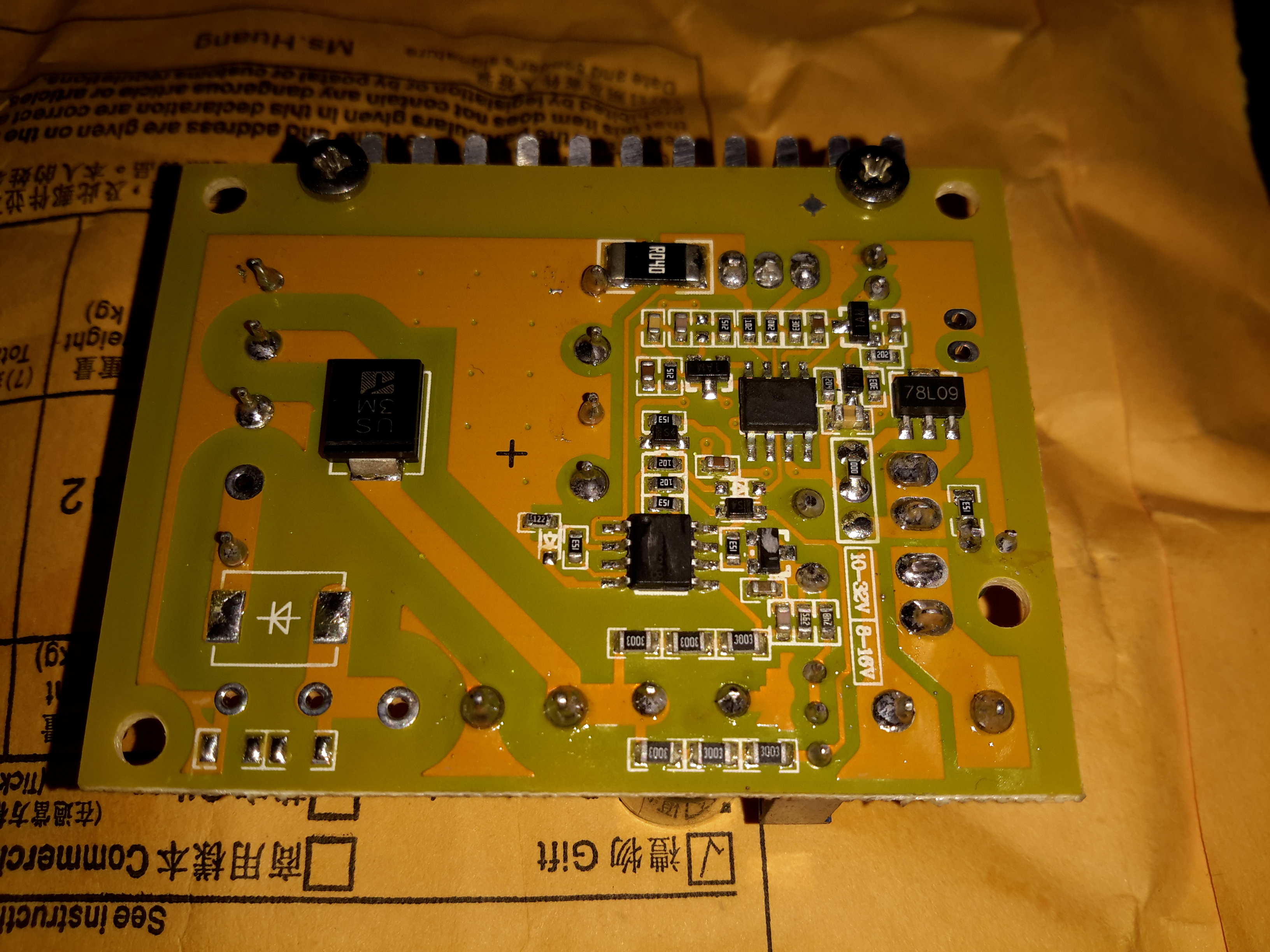
PCB Bottom
The bottom of the board has the control components, with a pair of ICs. Unfortunately the numbers have been scrubbed off, so no identification here. The output from the transformer is rectified with a single large SMD diode on the left side of the board.
There’s also plenty of isolation gap between the HV output trace & the low voltage logic side of the circuit, the two being bridged only by a resistive divider for output voltage measurement.
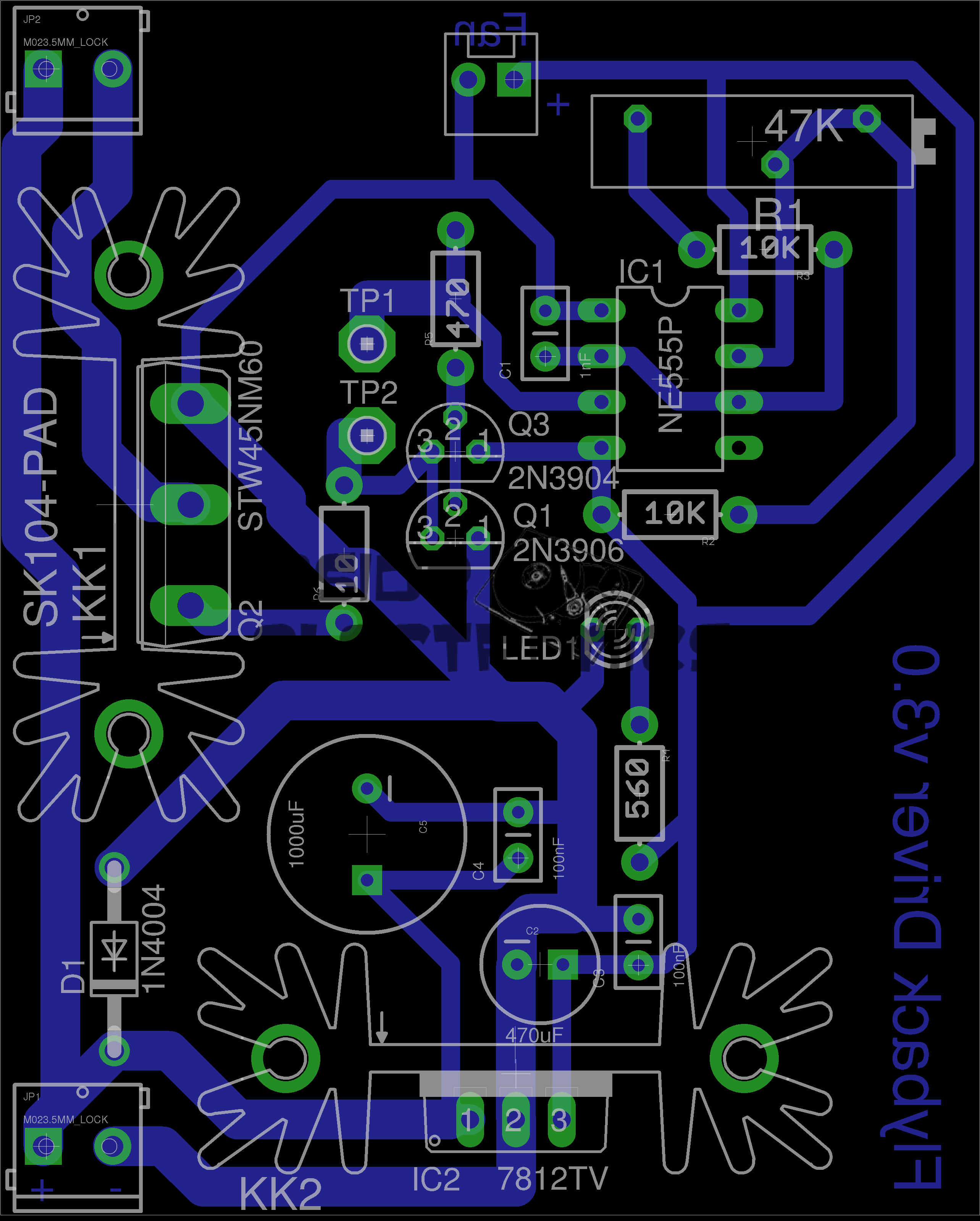
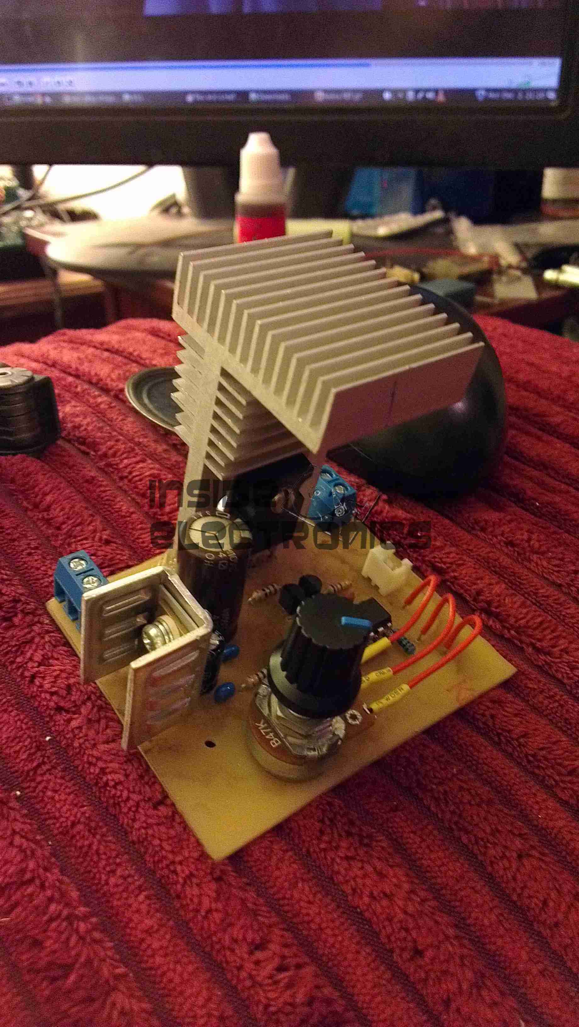
Here is a simple 555 timer based flyback transformer driver, with the PCB designed by myself for some HV experiments. Above is the Eagle CAD board layout.
The 555 timer is in astable mode, generating a frequency from about 22kHz to 55kHz, depending on the position of the potentiometer. The variable frequency is to allow the circuit to be tuned to the resonant frequency of the flyback transformer in use.
This is switched through a pair of buffer transistors into a large STW45NM60 MOSFET, rated at 650v 45A.
Input power is 15-30v DC, as the oscillator circuit is fed from an independent LM7812 linear supply.
Provision is also made on the PCB for attaching a 12v fan to cool the MOSFET & linear regulator.
Initial Board
Board initially built, with the heatsink on the linear regulator fitted. I used a panel mount potentiometer in this case as I had no multiturn 47K pots in stock.
PCB Traces
Bottom of the PCB. The main current carrying traces have been bulked up with copper wire to help carry the potentially high currents on the MOSFET while driving a large transformer.
This board was etched using the no-peel toner transfer method, using parchement paper as the transfer medium.
MOSFET Heatsinked
Main MOSFET now fitted with a surplus heatsink from an old switchmode power supply. A Fan could be fitted to the top of this sink to cope with higher power levels.
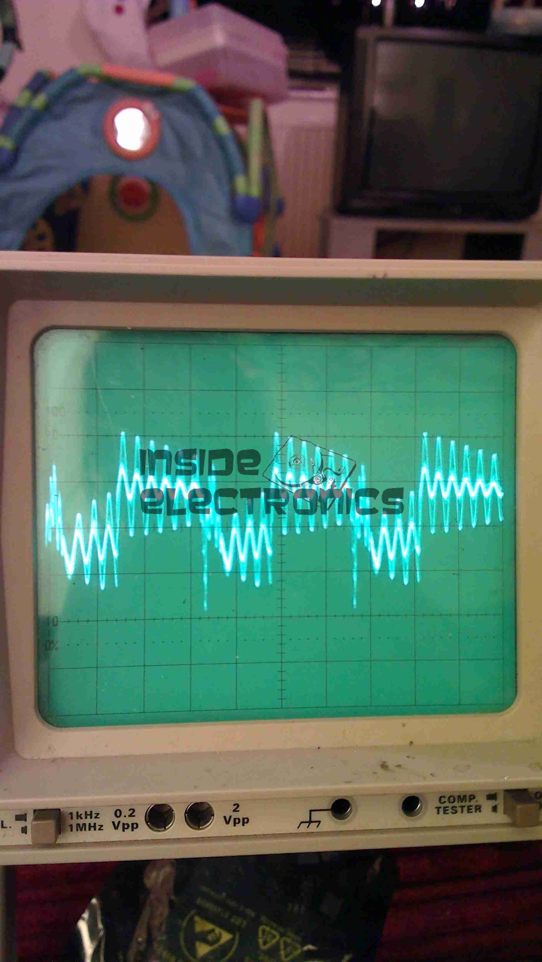
Gate Drive Waveform
This is the gate drive waveform while a transformer is connected, the primary is causing some ringing on the oscillator. The waveform without an attached load is a much cleaner square wave.
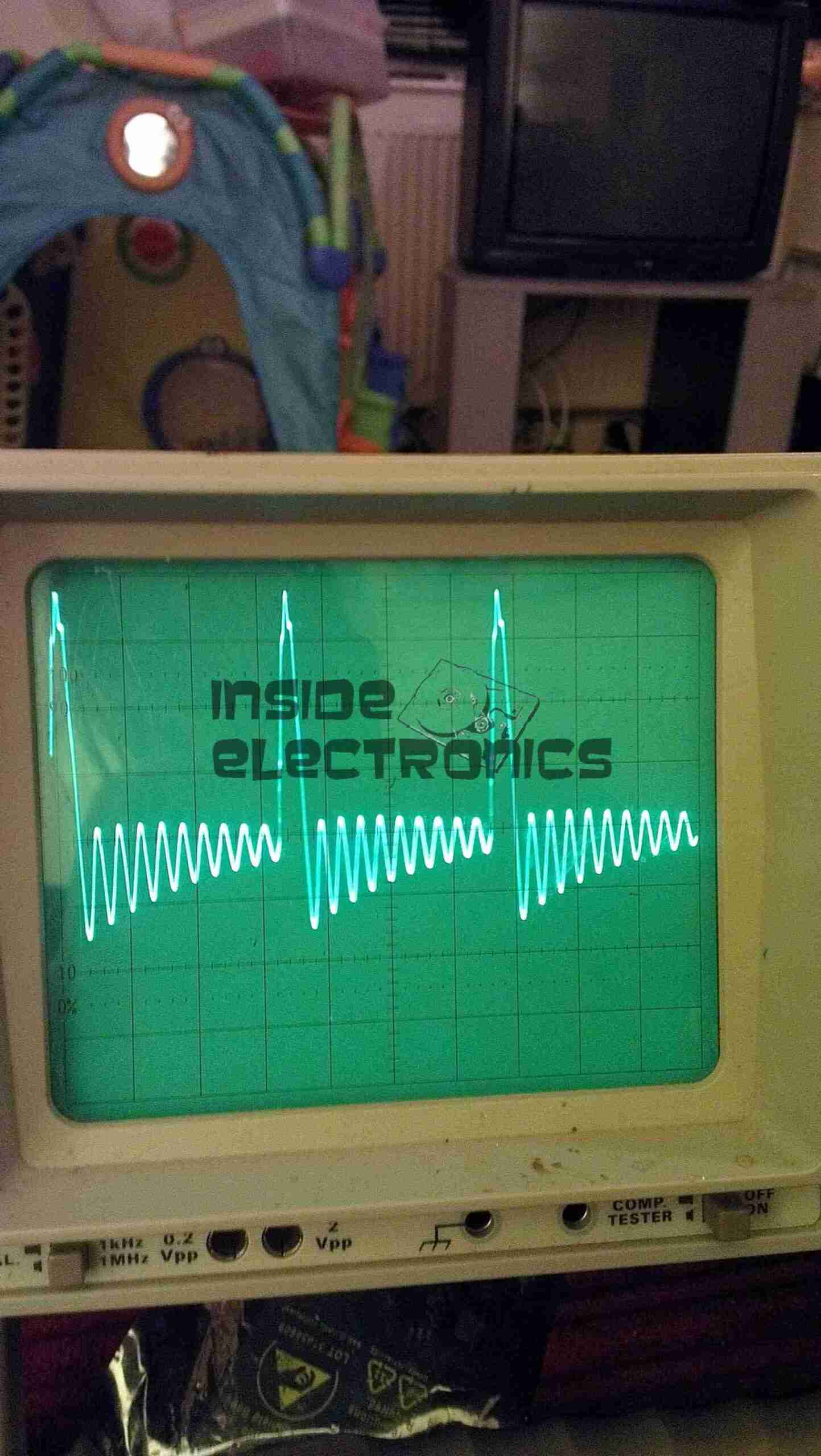
Flyback Secondary Waveform
I obtained a waveform of the flyback secondary output by capacitively coupling the oscilloscope probe through the insulation of the HT wire. The pulses of HV can be seen with the decaying ringing of the transformer between cycles.
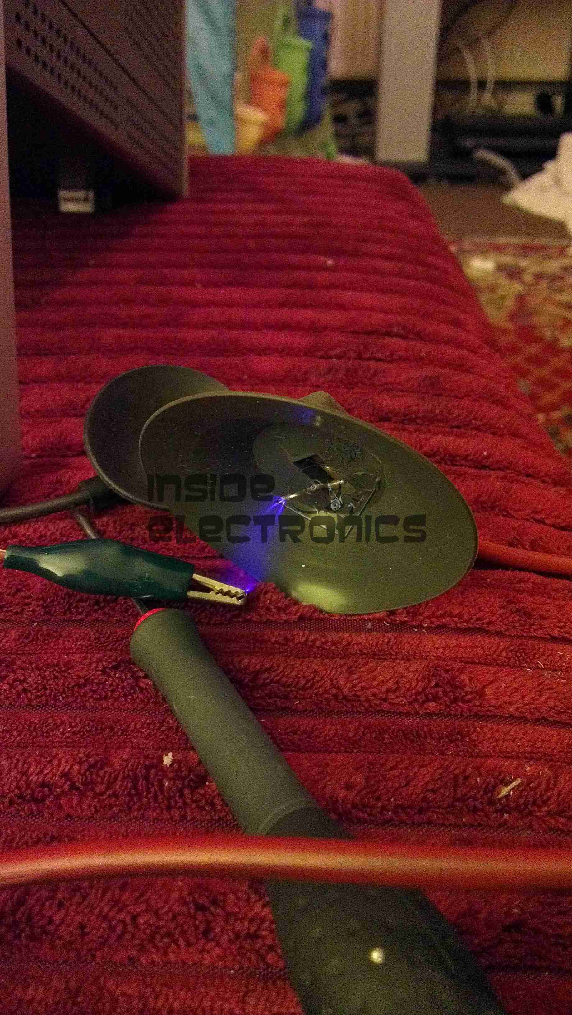
Corona DischargeArc Discharge
Corona & arc discharges at 12v input voltage.
Download the Eagle schematic files here: [download id=”5561″]
Here is a cheap no frills microwave oven, which died after a few weeks of normal use.
Electronics Bay
Cover removed, showing the internals. Front of the microwave is on the left.
Timer
Closeup of the timer unit. Cheap & nasty.
Magnetron
Magnetron removed from the oven. Antenna is on the top, cooling fins visible in the center. White conector at the bottom is the filament terminals.
Magnetron Chokes
Chokes on the magnetron’s filament connections. These prevent microwave energy from feeding back into the electronics bay through the connections.
Magnetron Assembly
Magnetron cooling fins, tube & magnets removed from the frame.
Magnetron Tube
Bare magnetron tube.
Power Input Board
This PCB does some rudimentary power conditioning, power resistors are in series with the live feed to the power trasformer, to prevent huge power up surge. When the transformer energizes the relay, which is in parallel with the resistors, switches them out a fraction of a second after, providing full power to the transformer.
Standard RFI choke & capacitor at the top of the board, with the input resistor.
Transformer
Power transformer to supply the magnetron with high voltage.
Power output is ~2kV at ~0.5A. Pair of spade terminals are the low voltage filament winding.
Capacitor
HV Capacitor. This along with the diode form a voltage doubler, to provide the magnetron with ~4kV DC.
Diode
HV diode stack.
Fuse Element
Internals of the HV fuse. Rated for ~0.75A at 5kV. The fuse element is barely visible attached to the end of the spring. Connects between the transformer & the capacitor.
Cooling Fan
Cooling fan for the magnetron. Drive is cheap shaded pole motor.
Fan Motor
Fan motor. Basic 240v shaded pole induction type.
Tip Jar
If you’ve found my content useful, please consider leaving a donation by clicking the Tip Jar below!
All collected funds go towards new content & the costs of keeping the server online.