Posted on Leave a comment

Sony Xperia Z3 50% Battery Problems

Recently my phone decided it was going to die a battery-related death, and having not found much useful information on the Great Google, (all the information I could find, was hinting at many issues from firmware to a faulty motherboard, nobody seems to have actually done any investigation into similar issues), I decided to dig into the phone to try & repair the problem.

Broken Flex
Broken Flex

The phone would work correctly for a while, then with the slightest movement or knock, would spontaneously switch off, and not turn back on without being whacked on a hard surface.
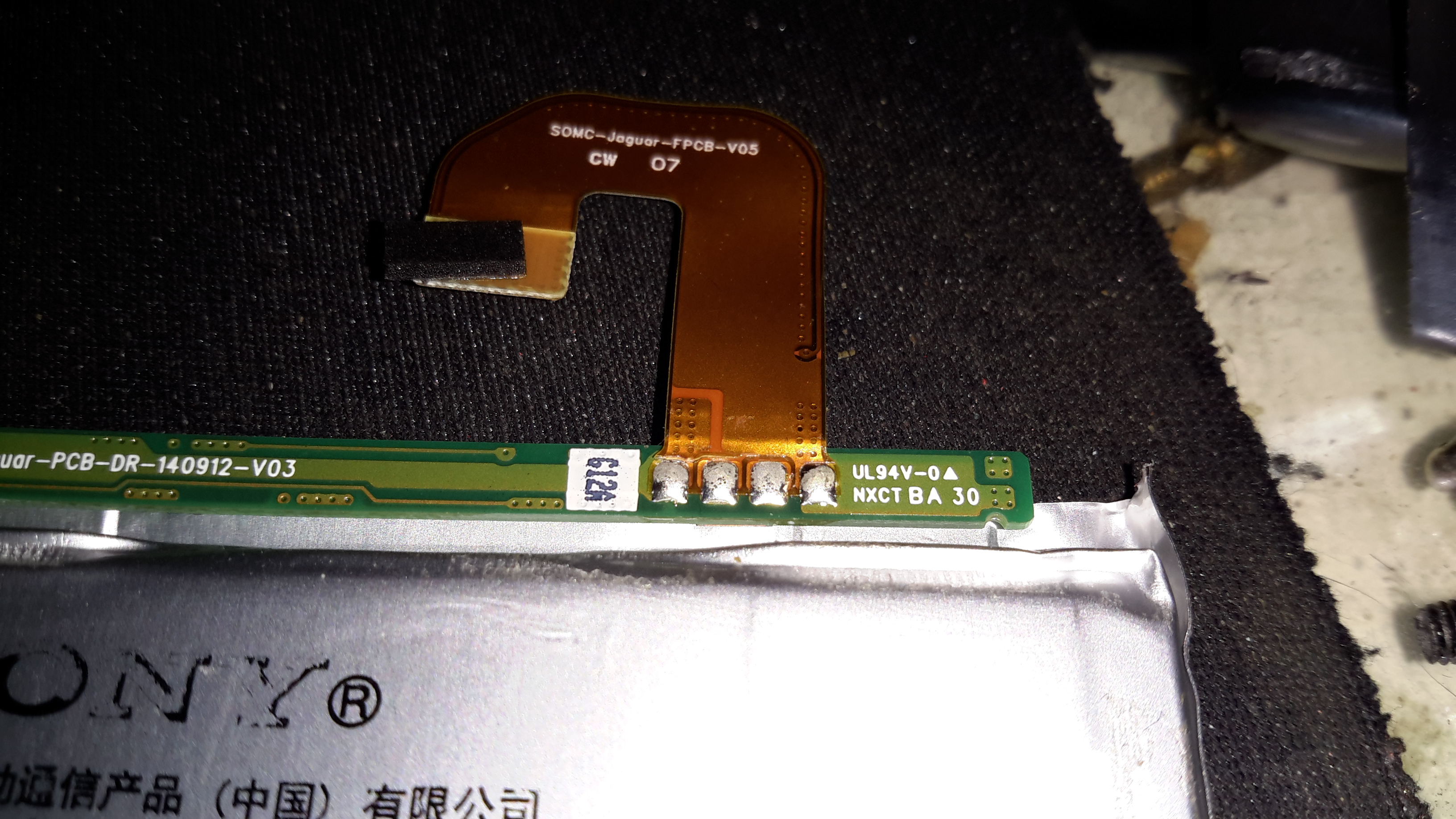
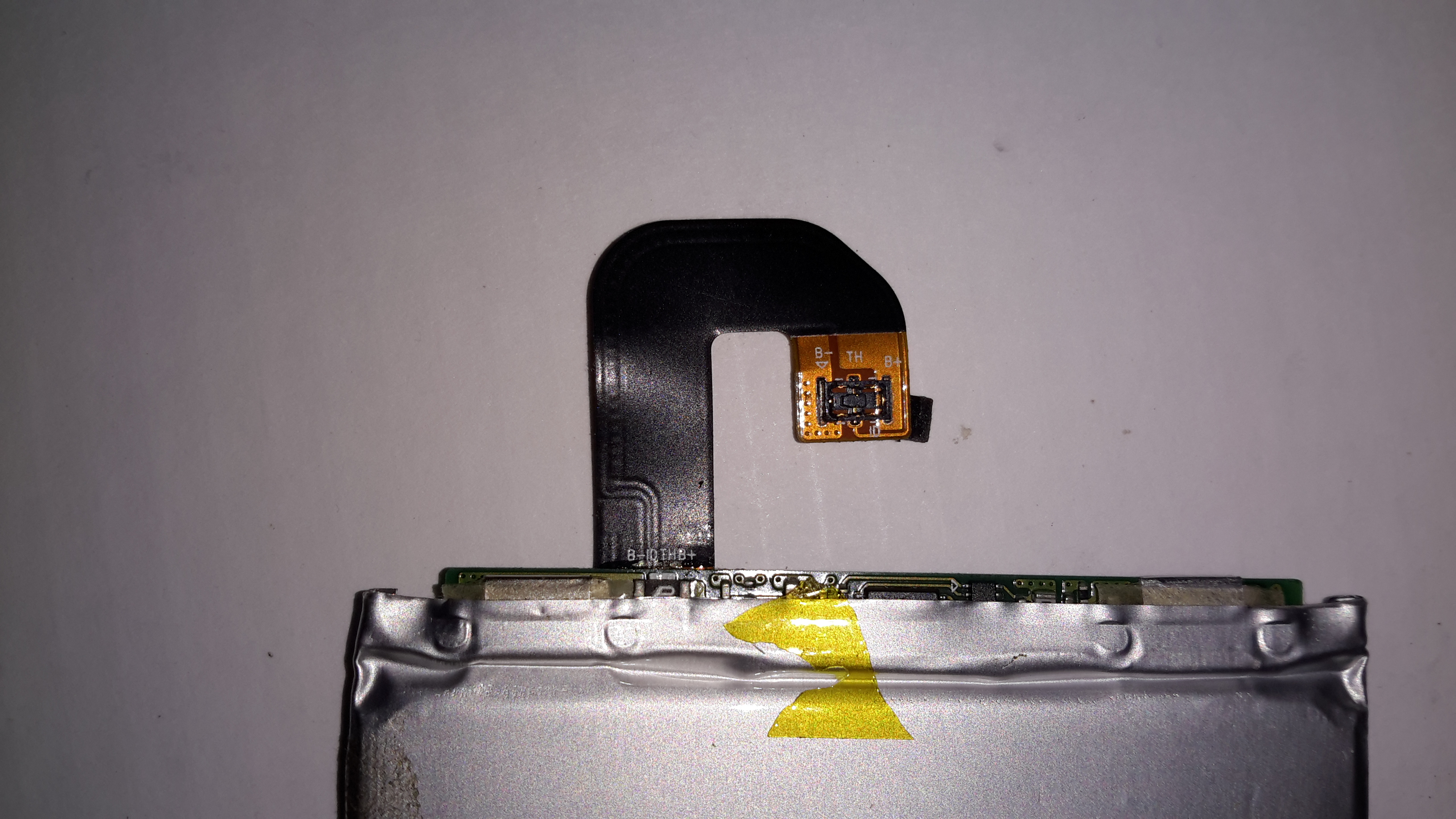
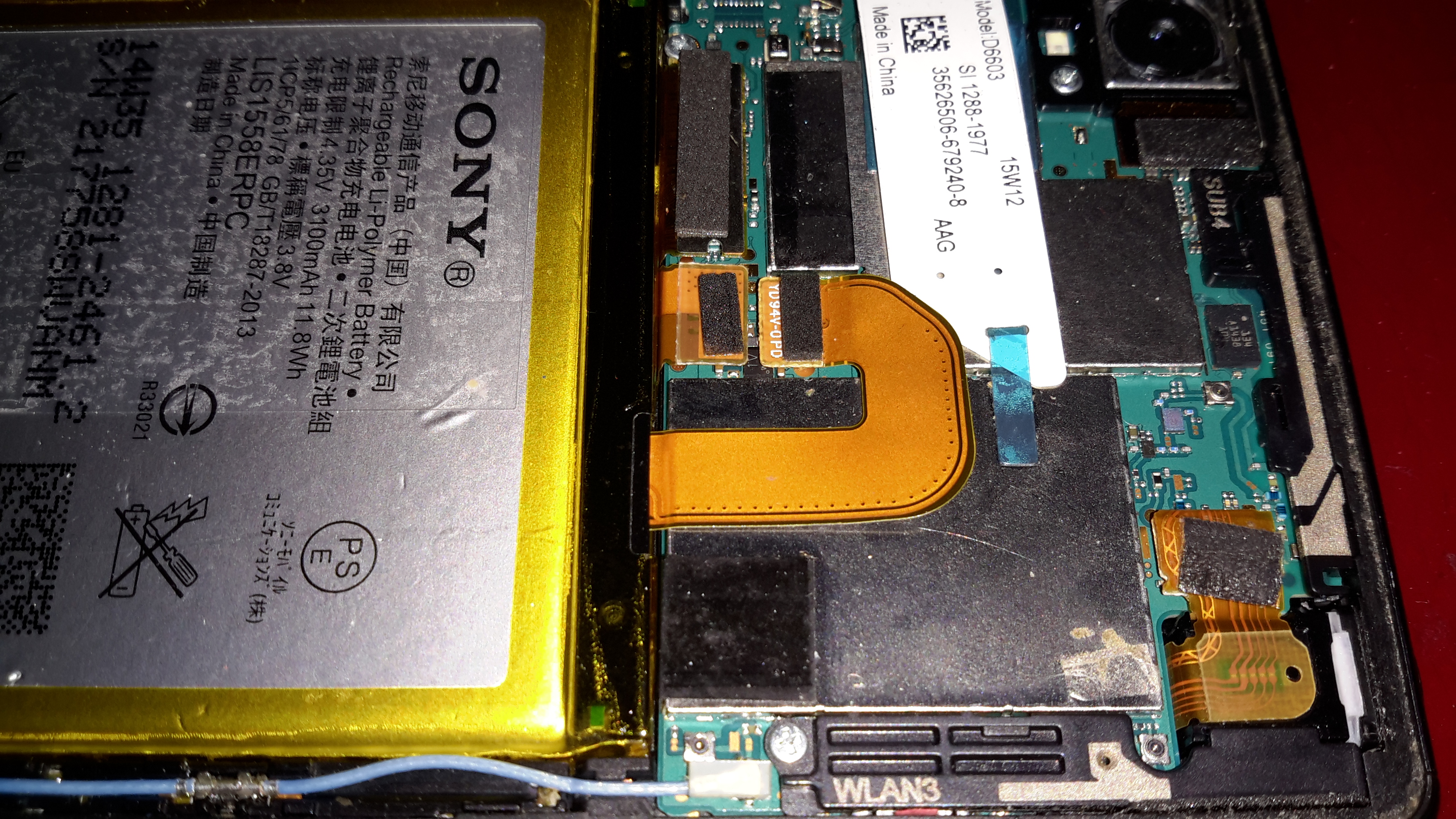
This symptom pointed me at a power connection problem. After removing the back of the phone (glass & heavily glued in place, so an awkward process), This was what I was presented with on the cell flex PCB.
In the above photo, the positive connection to the flex is fractured just after the solder joint with the BMS board.

Flex Repair
Flex Repair

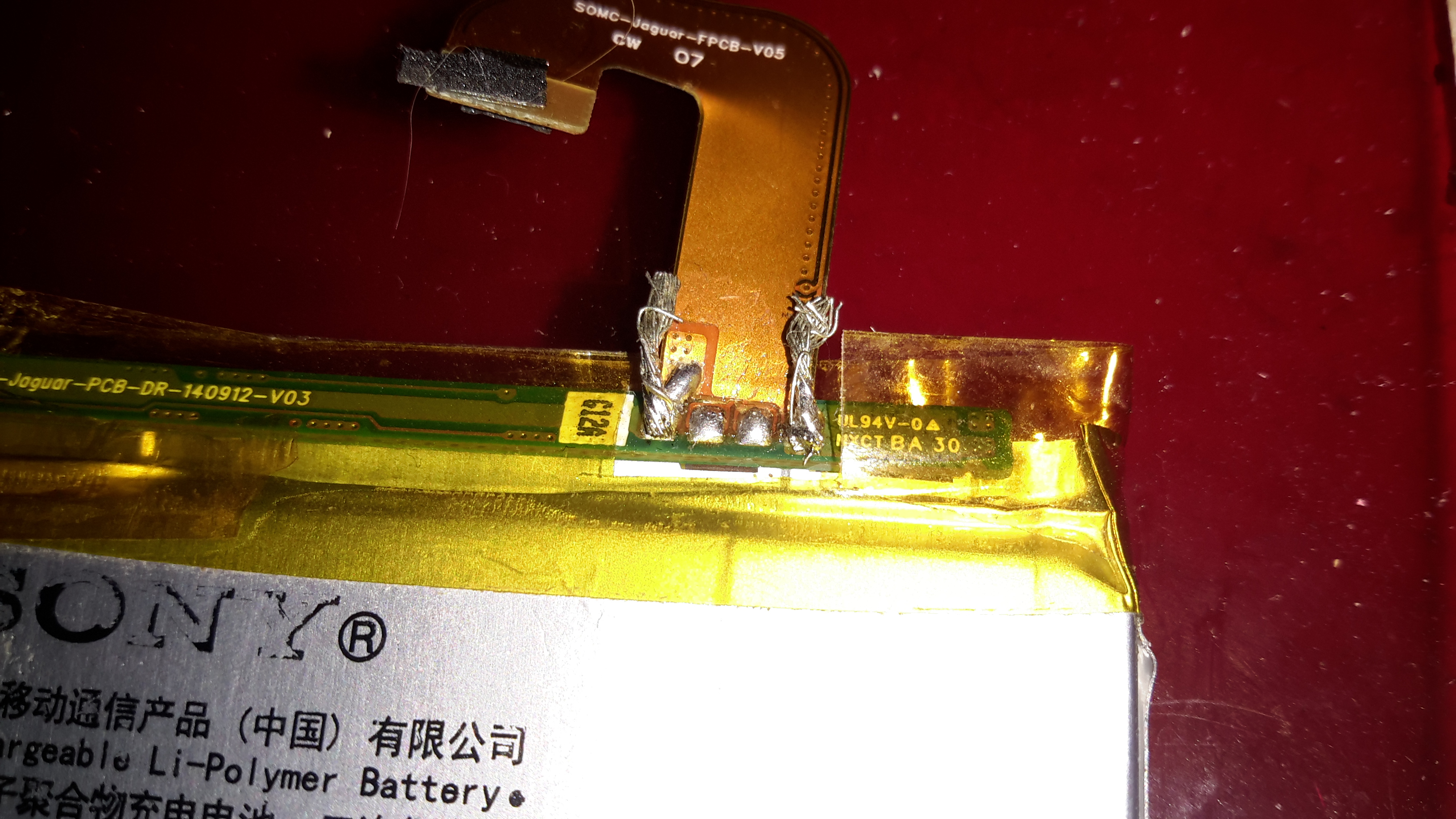
I managed to scrape some of the insulation off the flex PCB & solder a jumper on to restore power. Unfortunately, this repair generated another fault, where the battery level was always shown at 50%, and plugging into a USB supply wouldn’t charge the phone. The other two pins on the cell are for communication & temperature sensing, clearly one of these traces was also broken in the flex.
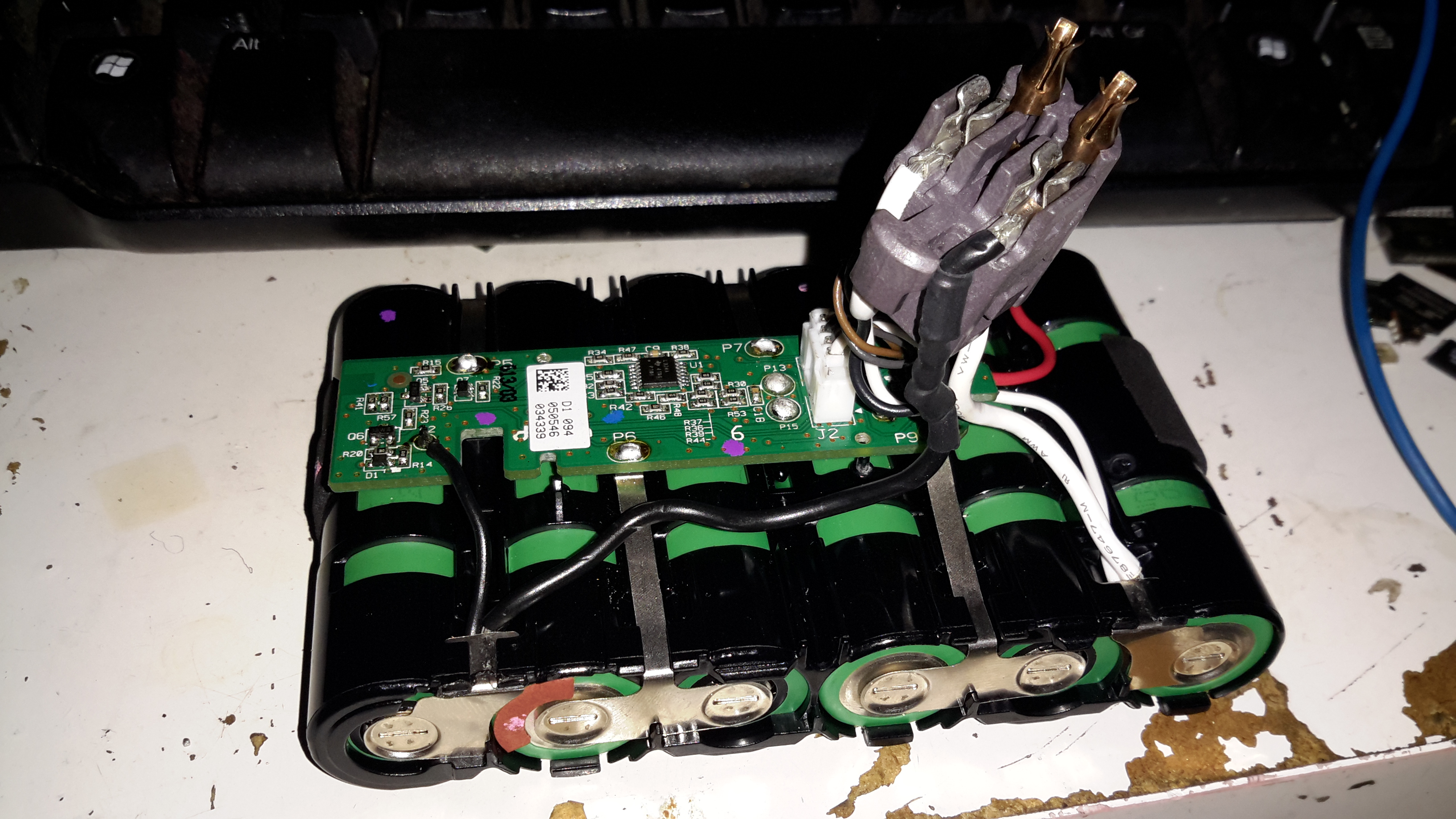
The above photo has a pair of very small wire tails as well, for connecting an external charger.

50% Battery
50% Battery

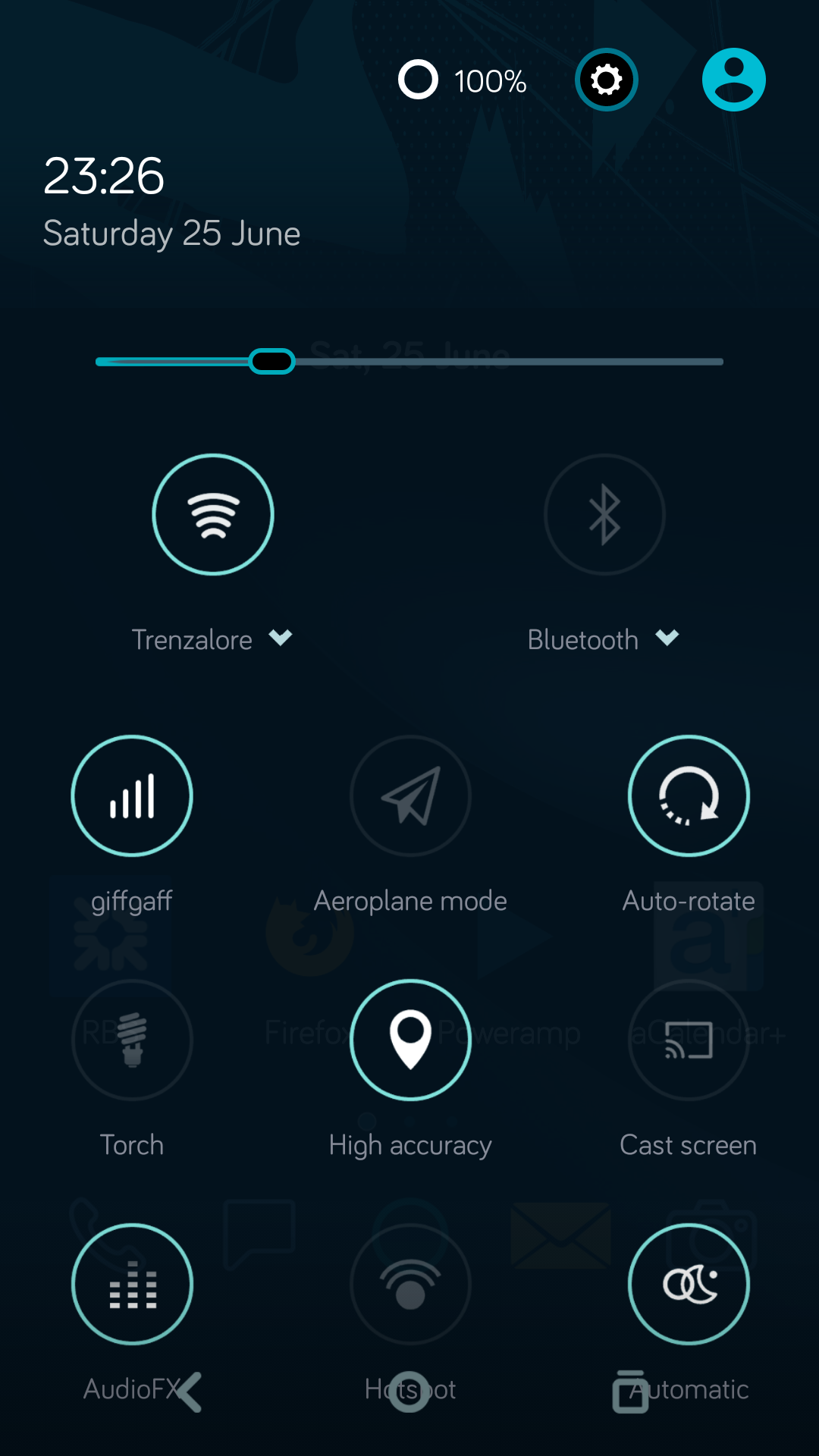
Here’s a screenshot of the phone with the original cell, even though it’s at about 4.15v (virtually fully charged). The battery management is having trouble talking to the phone, so for safety reasons, the charging logic refuses point-blank to charge the thing up.

Flex Cable
Flex Cable

The connector on the cell & phone motherboard is absolutely tiny, so I didn’t fancy attempting to solder on any bridge wires to try & bypass the broken flex.

Battery BMS
Battery BMS

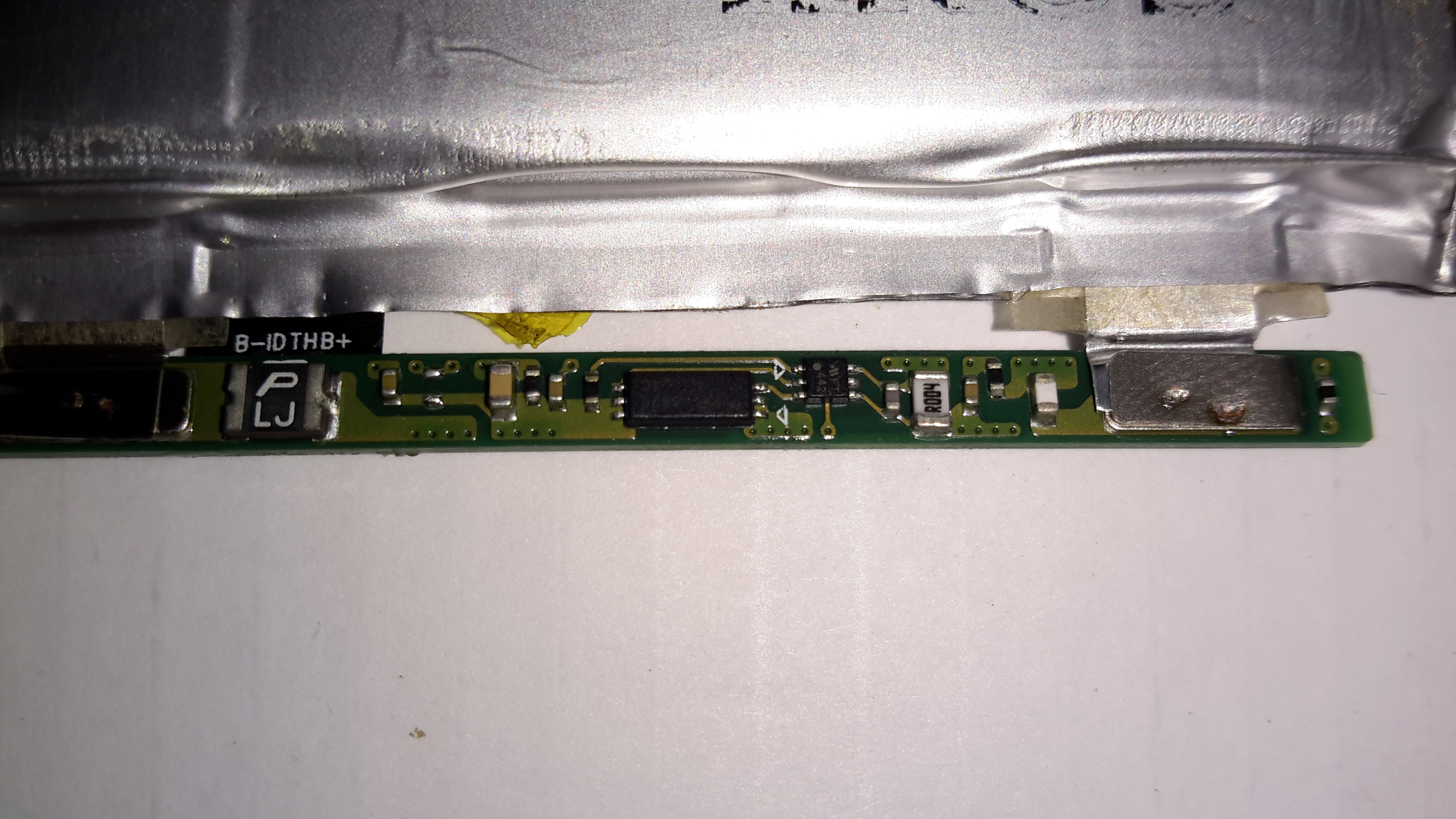
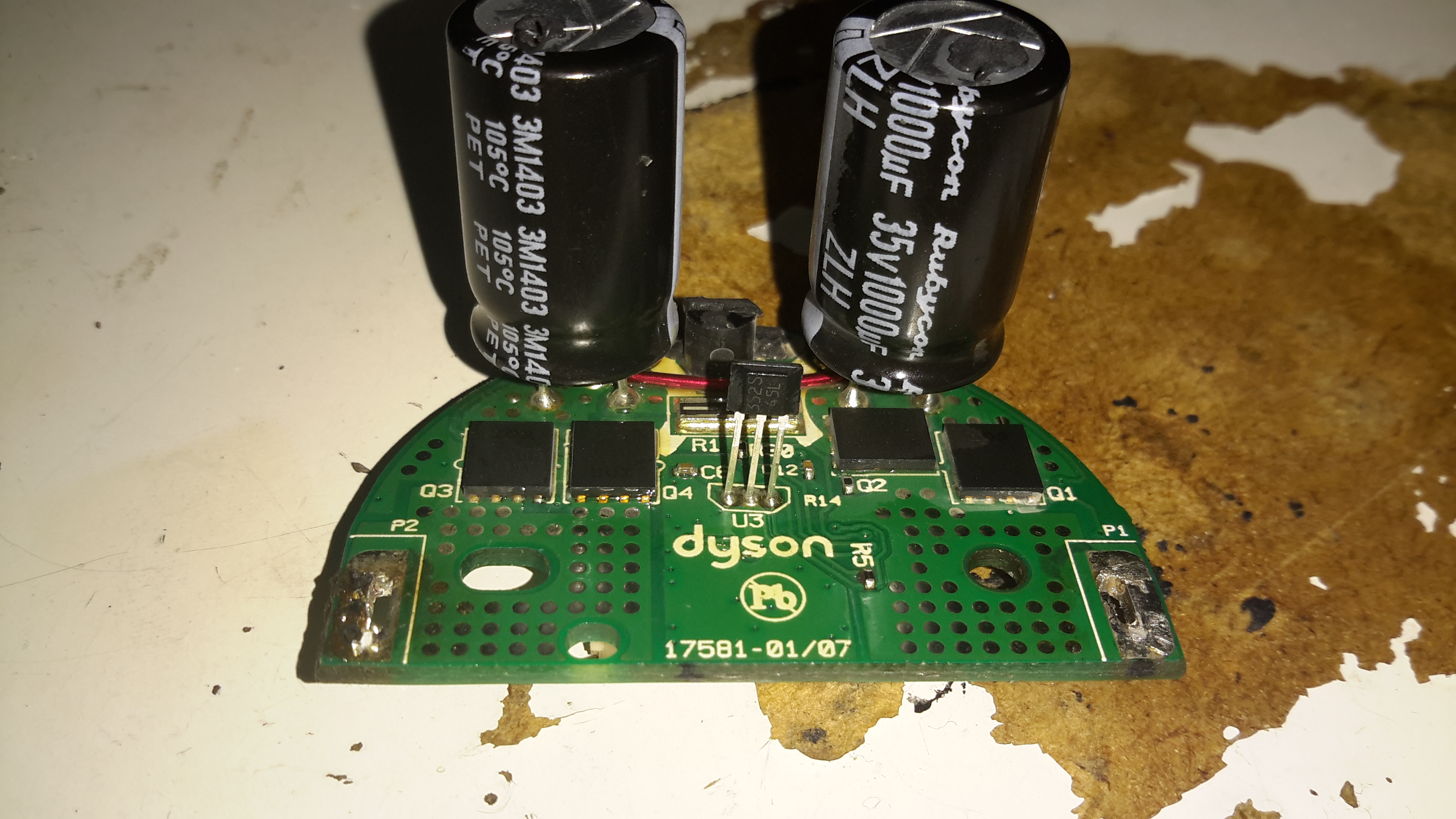
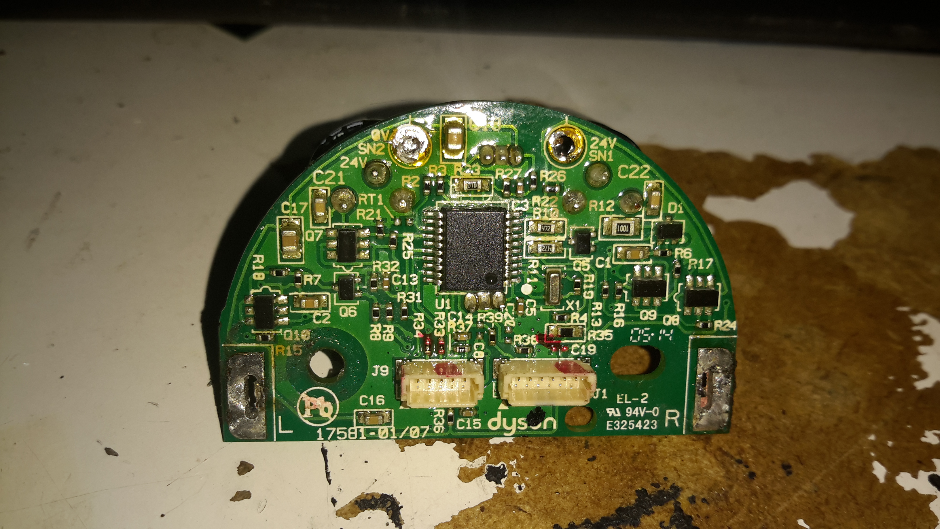
The cell BMS has some intelligence on board, besides the usual over-current, over-charge & under-charge protection. The very small IC on the right has a Microchip logo, and the marking FT442, but I was unable to dig up any datasheets. The current sense resistor is directly connected to this IC, along with the main power FET to the left.

BMS Reverse
BMS Reverse

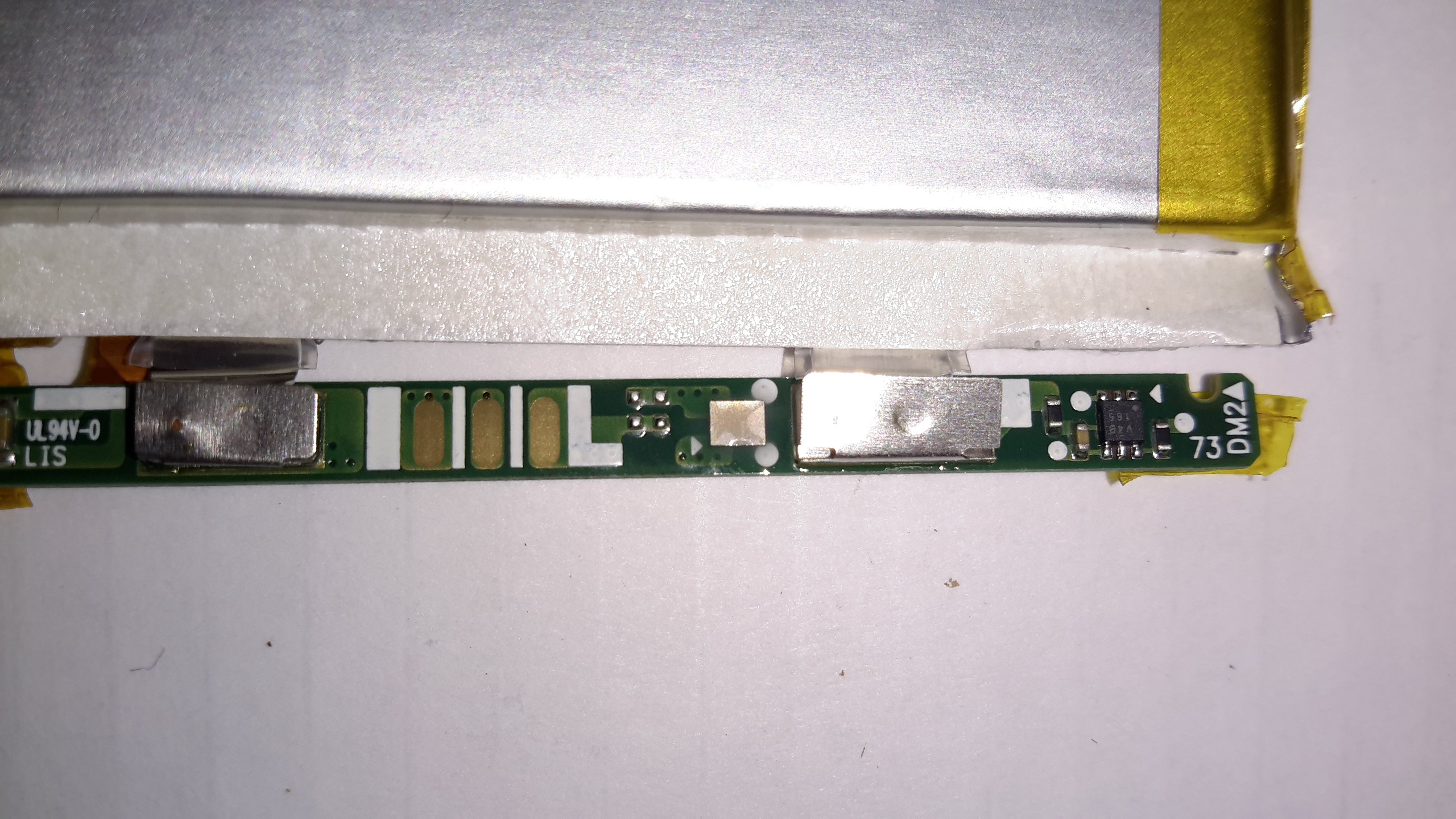
On the other side of the BMS board is another IC, again unidentifiable, and what looks like a bare-die, or CSP IC.

20160625_233656

At this stage I figured the only way forward was to buy a new battery, eBay turned one up for less than £5. Above is the new battery fitted to the phone, datestamped 2014, so definitely old stock.

100% Battery
100% Battery

Booting the phone with the new battery quickly lets me know the fix worked, with a 100% reading & the ability to again charge properly!

Posted on 69 Comments

Dyson DC35 “Digital” Teardown

DC35
DC35

Here’s another Dyson teardown, in my efforts to understand how marketing have got hold of relatively simple technology & managed to charge extortionate amounts of money for it.
This is the DC35, the model after the introduction of the brushless digital motor.

Back Cap Removed
Back Cap Removed

On this version the mouldings have been changed, and the back cover comes off, after removing the battery retaining screw. It’s attached with some fairly vicious clips, so some force is required. Once the cap is removed, all the electronics are visible. On the left is the motor itself, with it’s control & drive PCB. There’s another PCB on the trigger, with even more electronics. The battery connector is on the right.

Trigger PCB
Trigger PCB

Here’s the trigger PCB, which appears to deal with DC-DC conversion for powering the brush attachments. The QFN IC with yellow paint on it is an Atmel ATTiny461 8-bit microcontroller. This is probably controlling the DC-DC & might also be doing some battery authentication.

"Digital Motor"
“Digital Motor”

Here’s the motor & it’s board. The windings on the stator are extremely heavy, which makes sense considering it’s rated at 200W. The main control IC is a PIC16F690 from Microchip. Instead of using an off the shelf controller, this no doubt contains software for generating the waveforms that drive the brushless motor. It also appears to communicate with the other PCBs for battery authentication.

Stator
Stator

Desoldering the board allows it to be removed from the motor itself. The pair of windings are connected in anti-phase, to create alternating North-South poles depending on polarity. Since the existing controller is unusable due to software authentication with the other parts, I might have a go at building my own driver circuit for this with an Arduino or similar.

Blower Assembly
Blower Assembly

The blower assembly is simple plastic mouldings, pressed together then solvent welded at the seam.

Impeller
Impeller

The impeller is just a centrifugal compressor wheel, identical to what’s used in engine turbochargers.

Motor Control Board
Motor Control Board

The inside face of the control PCB holds the 4 very large MOSFETs, IRFH7932PbF from International Rectifier. These are rated at 30v 20A a piece, and are probably wired in a H-Bridge. There’s a bipolar Hall switch to sense rotor position & rotation speed, and an enormous pair of capacitors on the main power bus.

Motor Control Board Reverse

Not much on the other side of the PCB other than the microcontroller and associated gate drive stuff for the FETs.

Battery Pack Opened
Battery Pack Opened

The battery pack is similar to the DC16 in it’s construction, a heavily clipped together plastic casing holding 6 lithium cells. In this one though there’s a full battery management system. The IC on the top of the board above is a quad Op-Amp, probably for measuring cell voltages.

Battery BMS Bottom
Battery BMS Bottom

The other side of the BMS board is packed with components. I wasn’t able to identify the QFN IC here, as it’s got a custom part number, but it’s most definitely communicating with the main motor MCU via I²C over the two small terminals on the battery connector.

Posted on Leave a comment

Uniden UBC92XLT Teardown

One bit of my equipment that I’ve never looked into is my scanner, a handheld Uniden unit. I got this when Maplin Electronics had them on special offer a few years ago.

Uniden Scanner
Uniden Scanner

Here’s the scanner itself, roughly the same size as a usual HT.

Back Cover Removed
Back Cover Removed

Here the back cover has been removed, and the main RF board is visible at the top of the stack. Unfortunately the shielding cans are soldered on this unit, so no looking under there 🙁
On the right hand side of the board next to the antenna input is the main RF filter network, and it’s associated switching. The RF front end is under the shield closest to the front edge.

Controls & 3.3v Regulator

On the other side of the PCB is the Volume & Squelch potentiometers, along with a dedicated 3.3v switching supply. An NJM2360A High Precision DC/DC converter IC controls this one. A 3.3v test point is visible next to the regulator.

RF Board Reverse
RF Board Reverse

Here’s the backside of the RF board, some more interesting parts here. There’s a pair of NJM3404A Single Supply Dual Op-Amp ICs, and a TK10931V Dual AM/FM IF Discriminator IC. This is the one that does all the back-end radio functionality. The audio amplifier for the internal speaker & external headphone jack is also on this PCB, top left. A board-to-board interconnect links this radio board with the main control board underneath.

Control PCB Front
Control PCB Front

Here’s the front of the control PCB, nothing much to see here, just the LCD & membrane keypad contacts.

Control PCB Reverse
Control PCB Reverse

And here’s the reverse side of the control board. All the interesting bits are here. The main microcontroller is on the right, a Renesas M38D59GF, a fairly powerful MCU, with onboard LCD drive, A/D converter, serial interface, 60K of ROM & 2K of RAM. It’s 6.143MHz clock crystal is just below it.
The mating connector for the RF board is in the centre here.

There is also a Microchip 24LC168 16KB I²C EEPROM next to the main microcontroller. This is probably for storing user settings, frequencies, etc.

EEPROM
EEPROM

The rest of this board is dedicated to battery charging and power supply, in the centre is a dual switching controller, I can’t figure out the numbers on the tiny SOT23 components in here, but this is dealing with the DC 6v input & to the left of that is the circuitry for charging the NiMH cells included with the scanner.

PSU
PSU

The last bit of this PCB is a BU2092FV Serial In / Parallel Out 4 channel driver. Not sure what this one is doing, it might be doing some signal multiplexing for the RF board interface. Unfortunately the tracks from this IC are routed on the inner layers of the board so they can’t be traced out.

Posted on 2 Comments

Roving Networks RN-52 Bluetooth Audio

I’ve been doing some tinkering with the RN-52 Bluetooth Audio module from Roving Networks, in prep for building a portable wireless speaker system, & thought I’d share my designs.

Initially I was having some issues with RF noise on the audio output from the RN-52, as I was only using the outputs single-ended. The module didn’t like this treatment, with all the RF whine coming straight out of the speakers.

To fix this issue I have used a pair of jellybean LM386 audio power amplifiers, running in differential input mode. This solves the high-pitched whine when the audio is enabled, & also allows the module to directly drive a set of 32Ω headphones at a reasonable level.

In Eagle I have designed a simple board, routing only the audio output, serial TTL & command mode pins out, along with the supporting power supply circuitry to operate from 12v DC.

RN-52 Breadboard
RN-52 Breadboard

Above is the current incarnation of the circuit on the breadboard. The RN-52 is on the left, audio power stage in the centre & headphone output on the right.

RN-52 Breakout
RN-52 Breakout

The bluetooth module on a breakout board. I was cheap in this case & etched my own board. I’m not paying Sparkfun, (as much as I like them), an extra ~£10 for a small PCB with the pins broken out. Much cheaper to spend 15 minutes with the laser printer & the iron, & do a toner transfer PCB.
As this board is single sided, I added a ground plane on the underside with copper foil, to help with the RF issues. Breadboards really aren’t all that good at rejecting noise induced when there’s a 2.4GHz transceiver mounted on them.

LM386 Amplifier
LM386 Amplifier

The LM386 audio power stage. The differential inputs from the module are capacitively coupled with 1µF electrolytics. This setup remarkably reduced the noise on the output. I left these at their default gain of 20, as I’ll be connecting another high power amplifier stage to drive large speakers.

RN-52 Eagle Layout
RN-52 Eagle Layout

Here’s the circuit laid out in Eagle, ready for PCB.

RN-52 Eagle PCB
RN-52 Eagle PCB

And here’s the PCB layout. Only one link required for the +5v line from the TTL serial port.

As always, the Eagle PCB & Schematic layout files are available at the bottom of the article.

*Update 29-01-15*
Rerouted a few things:

  • Moved the audio power stage to the +12v rail to improve sound response. – As the LM386 has a max input voltage of 12v (absolute maximum 15v), a regulated supply is recommended. The LM386-N4 variant has a higher voltage range, up to 18v. This should be suitable for an unregulated supply.
  • Removed 1µF coupling capacitors to reduce distortion & amplifier hiss. The capacitors appeared to cause some instability on the amplifier, causing random distortion. Removing them has cured this. No signal hiss has also been reduced to a very low level.
  • Reversed input polarity on input of one of the amplifiers – this appears to produce better audio.
  • Added PWR.EN header to allow connection of power button. Saves hassle of cycling power to the board when the RN-52 goes into sleep mode.

Improved PCB & Schematic layouts.

RN-52-SCH-v3.6
RN-52-SCH-v3.6
RN-52-PCB-v3.6
RN-52-PCB-v3.6

[download id=”5579″]

Posted on 2 Comments

Current Cost ‘Envi’ CC128 Power Meter

Display Unit
Display Unit

This is the Current Cost CC128 Real Time Power Meter. Shown here is the display unit, British Gas issued these free to some customers.
This unit measures current power draw in Watts, cost of power currently being used (requires unit price to be set), overall kWh usage over the past 1, 7 or 30 days & power trends during the day, night & evening. Also displays current time & current room temperature.

Display PCB
Display PCB

Here the front panel of the display has been un-clipped. At the bottom are the RJ-45 serial port & power connections.
This unit uses a PIC micro-controller as it’s CPU (PIC18F85J90) Just above & left of the CPU is the 433MHz SPD radio receiver module. The chips on the right of the CPU are a 25LC128 SPI serial EEPROM for data storage & a 74HC4060 14 stage binary counter, to which is connected the 32kHz clock crystal. The red wire around the top of the display is the antenna for the radio receiver.

For more info on the CC128 in general, the serial port & software for computer data logging, see this link
See this link for Current Cost’s list of software

Processor & Radio
Processor & Radio

Closeup of the ICs on the mainboard.

Transmitter Unit
Transmitter Unit

Here we have the transmitter unit, with Current Transformer (CT). The red clamp fits around one of the electric meter tails & read the current going to the various circuits. This unit is powered by 2x D cells, rated at a life of 7 years.

Transmitter PCB
Transmitter PCB

The PCB inside the transmitter. Again very minimal design, unknown controller IC, 433MHz radio transmitter on right hand side with wire antenna. Two barrel connectors on left hand side of board allow connection of up to two more CT clamps for measurement of 3-phase power. Centre of board is unmarked header. (ICSP?)

Current Transformer
Current Transformer

CT unit. Inside is a coil of wire & an iron core which surrounds the cable to be measured.