Here’s another Dyson teardown, in my efforts to understand how marketing have got hold of relatively simple technology & managed to charge extortionate amounts of money for it.
This is the DC35, the model after the introduction of the brushless digital motor.
On this version the mouldings have been changed, and the back cover comes off, after removing the battery retaining screw. It’s attached with some fairly vicious clips, so some force is required. Once the cap is removed, all the electronics are visible. On the left is the motor itself, with it’s control & drive PCB. There’s another PCB on the trigger, with even more electronics. The battery connector is on the right.
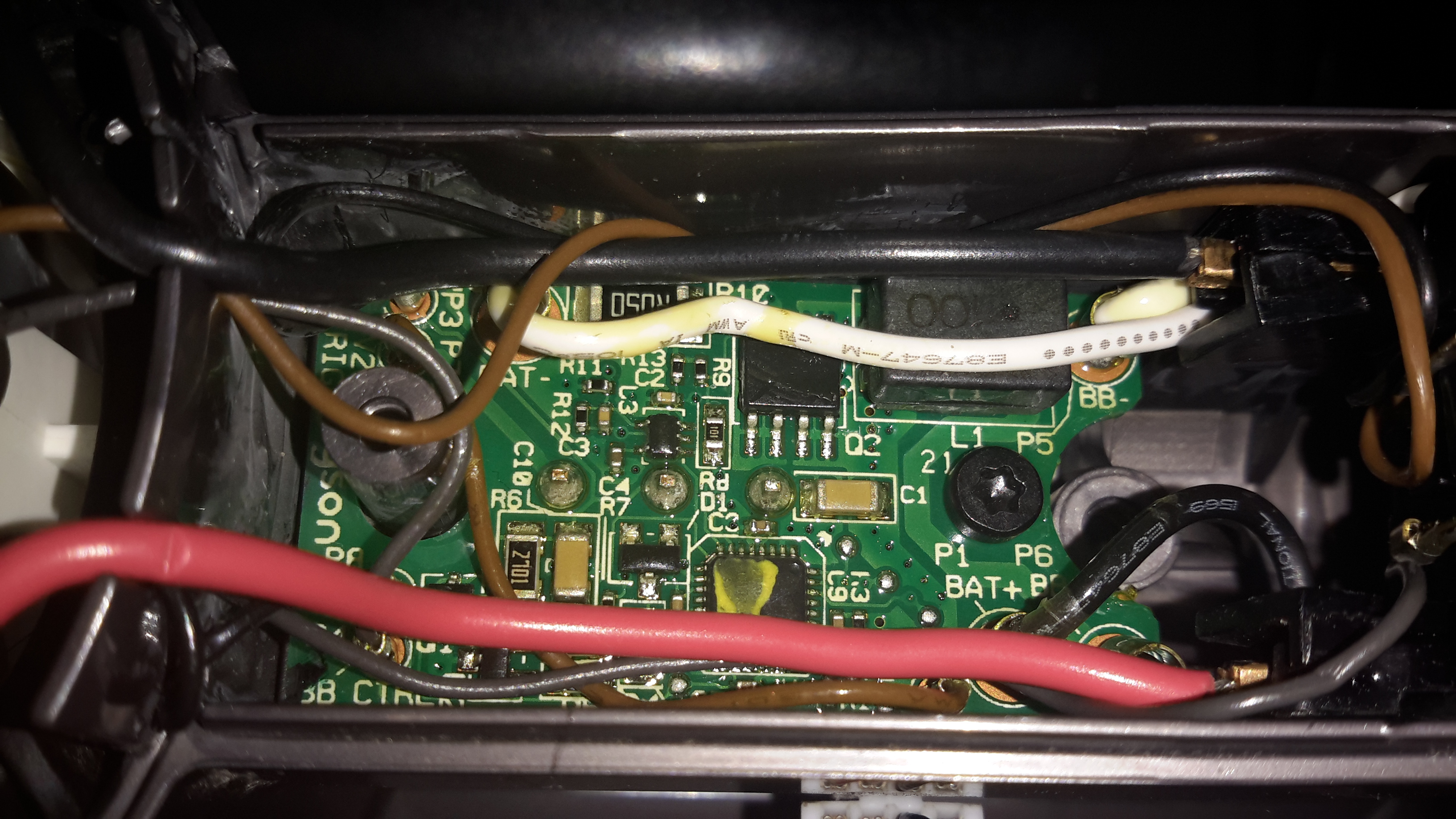
Here’s the trigger PCB, which appears to deal with DC-DC conversion for powering the brush attachments. The QFN IC with yellow paint on it is an Atmel ATTiny461 8-bit microcontroller. This is probably controlling the DC-DC & might also be doing some battery authentication.
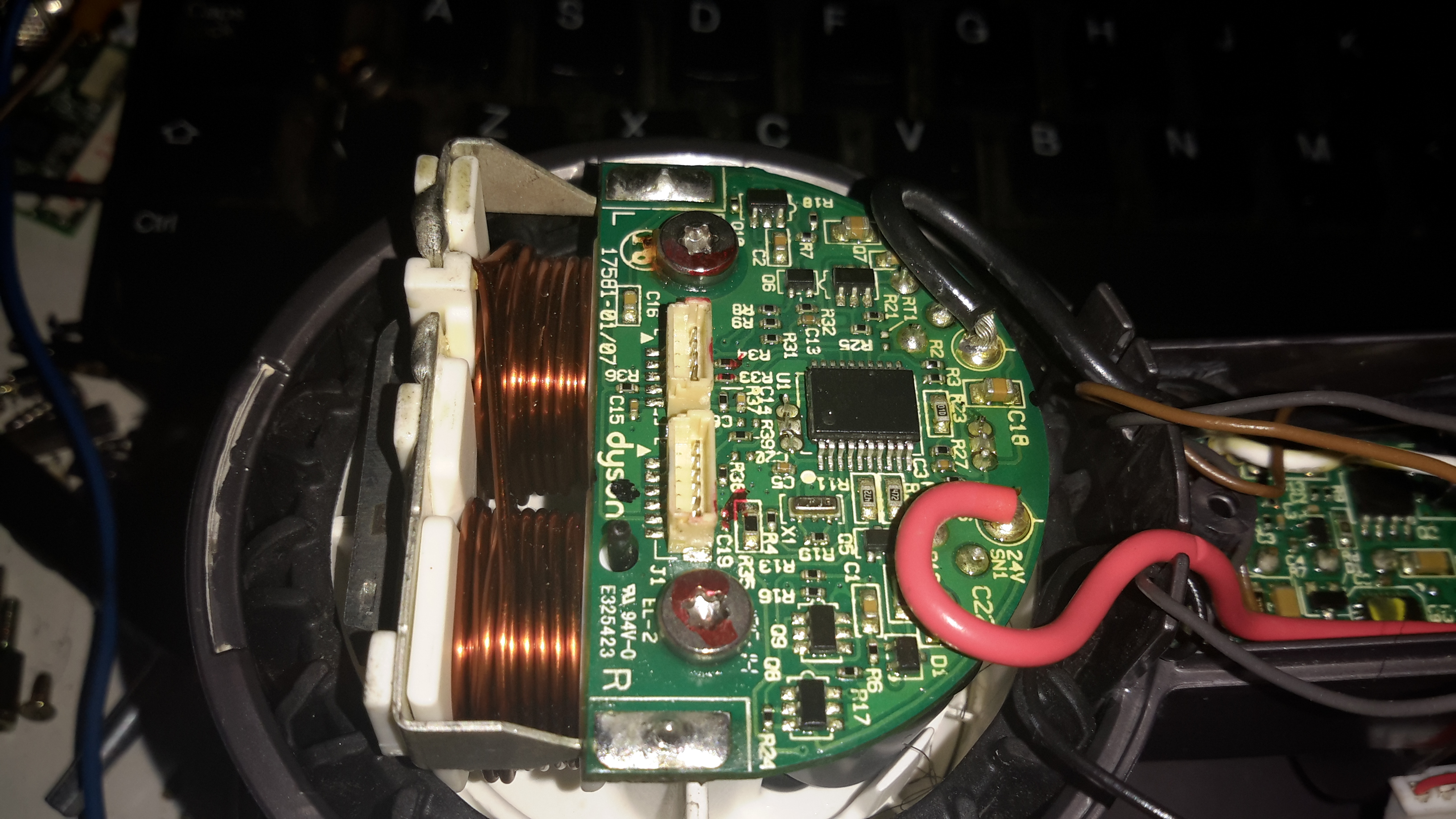
Here’s the motor & it’s board. The windings on the stator are extremely heavy, which makes sense considering it’s rated at 200W. The main control IC is a PIC16F690 from Microchip. Instead of using an off the shelf controller, this no doubt contains software for generating the waveforms that drive the brushless motor. It also appears to communicate with the other PCBs for battery authentication.
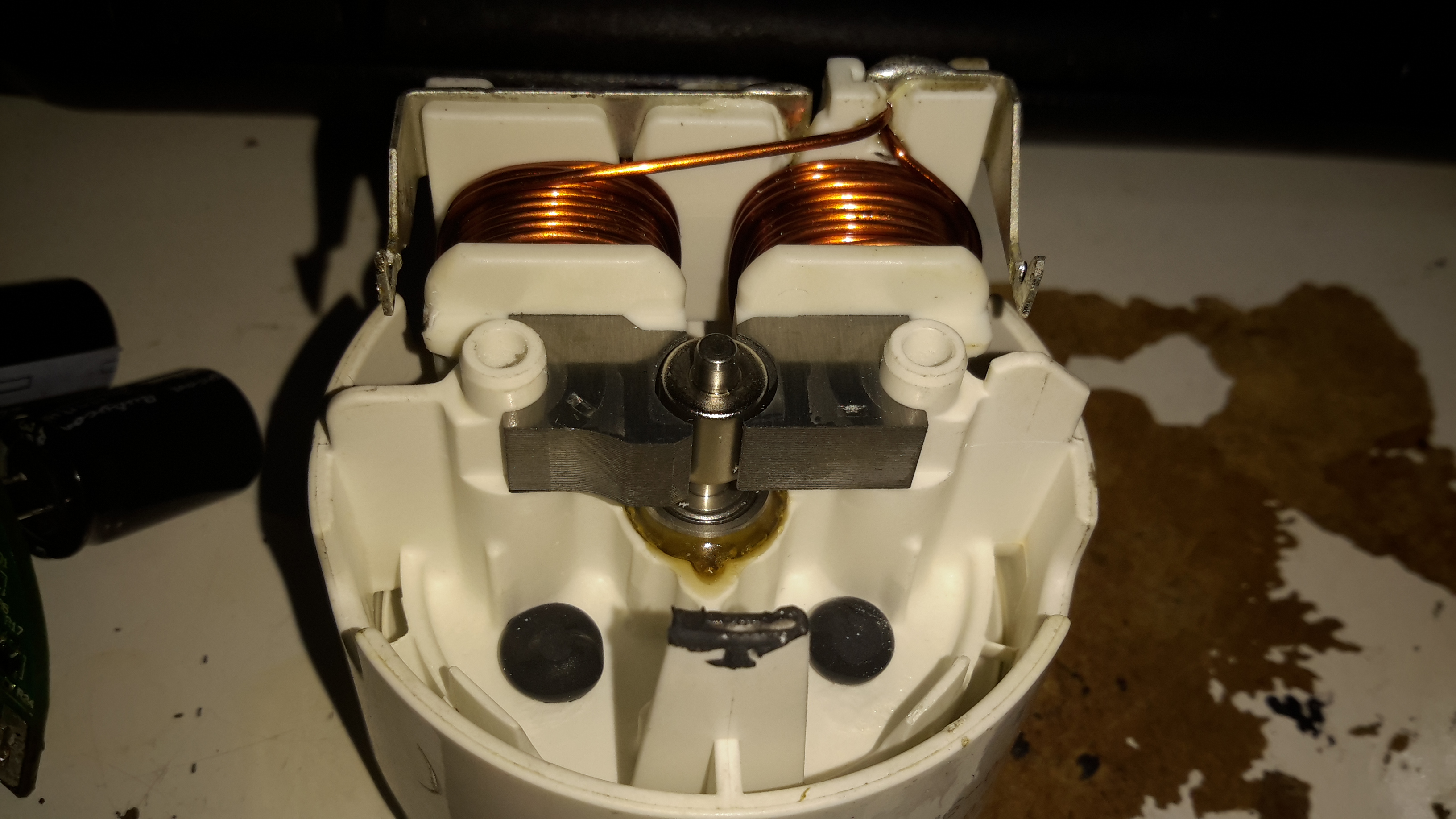
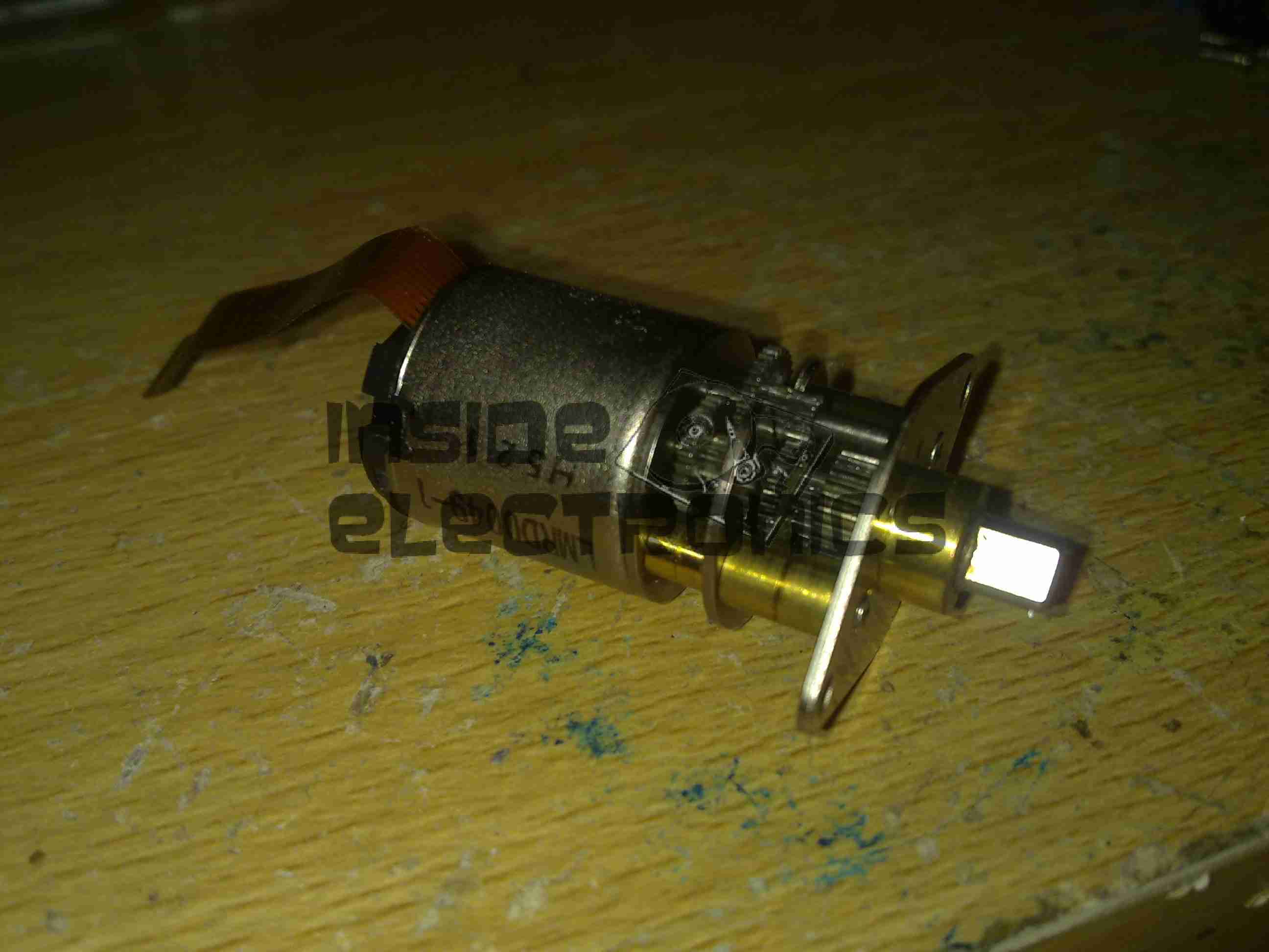
Desoldering the board allows it to be removed from the motor itself. The pair of windings are connected in anti-phase, to create alternating North-South poles depending on polarity. Since the existing controller is unusable due to software authentication with the other parts, I might have a go at building my own driver circuit for this with an Arduino or similar.
The blower assembly is simple plastic mouldings, pressed together then solvent welded at the seam.
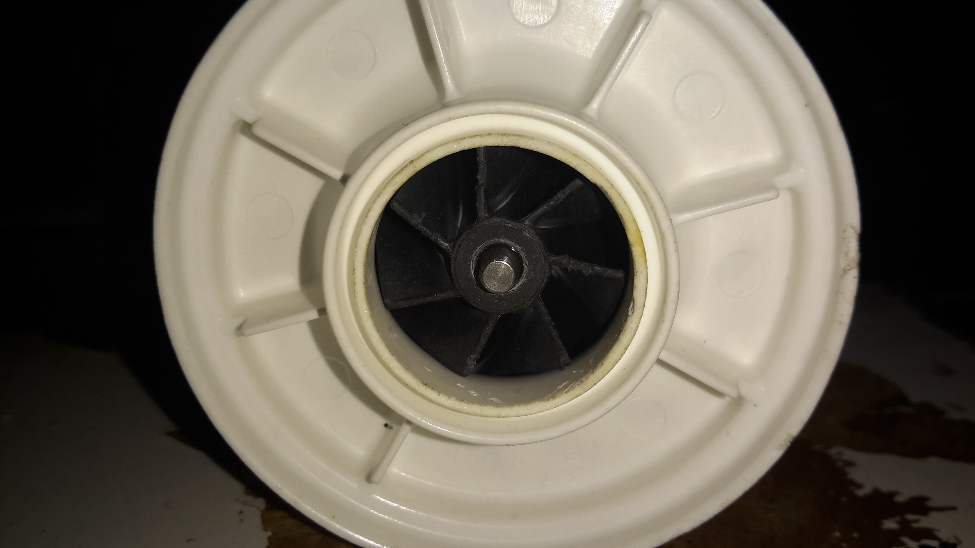
The impeller is just a centrifugal compressor wheel, identical to what’s used in engine turbochargers.
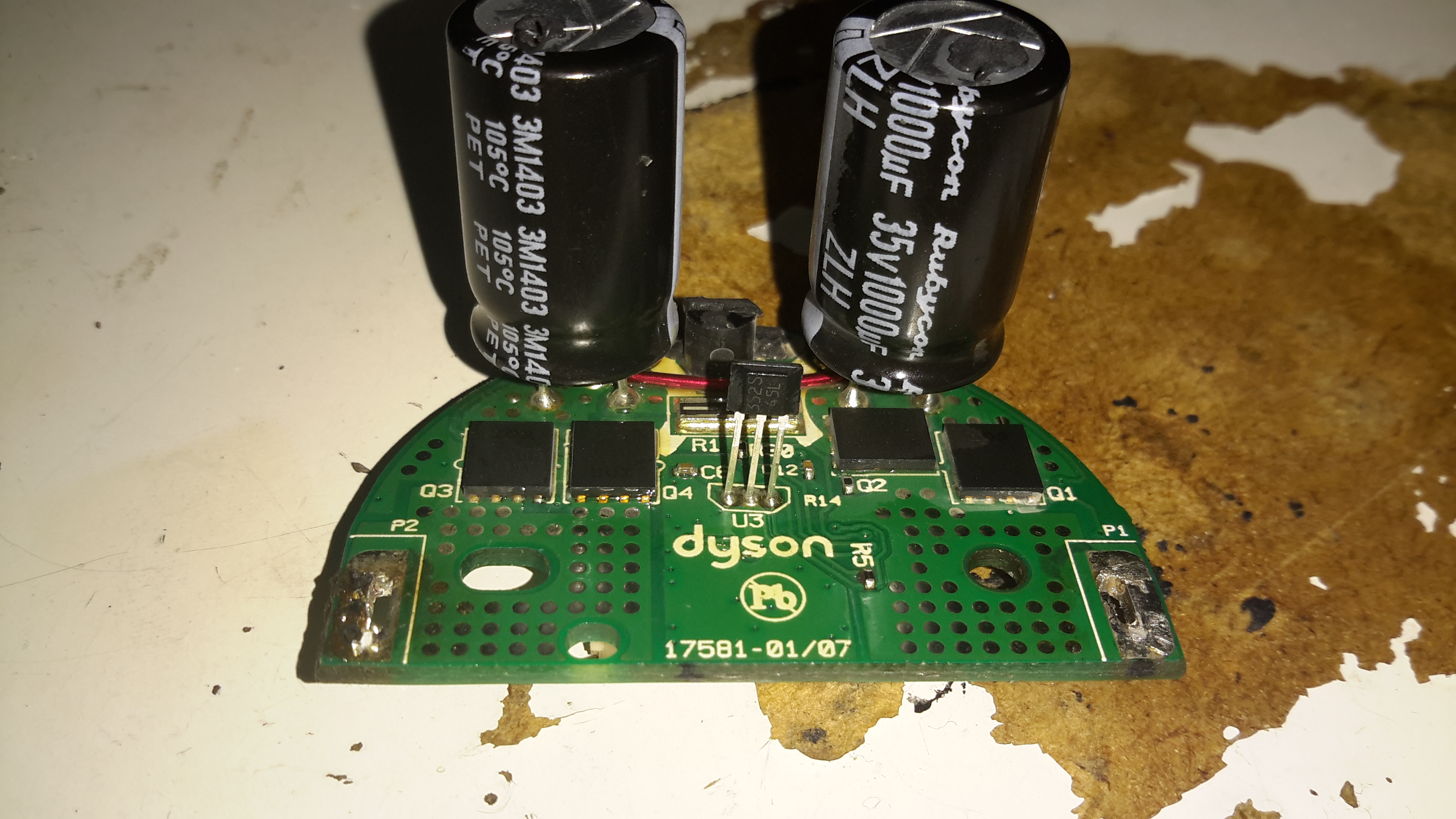
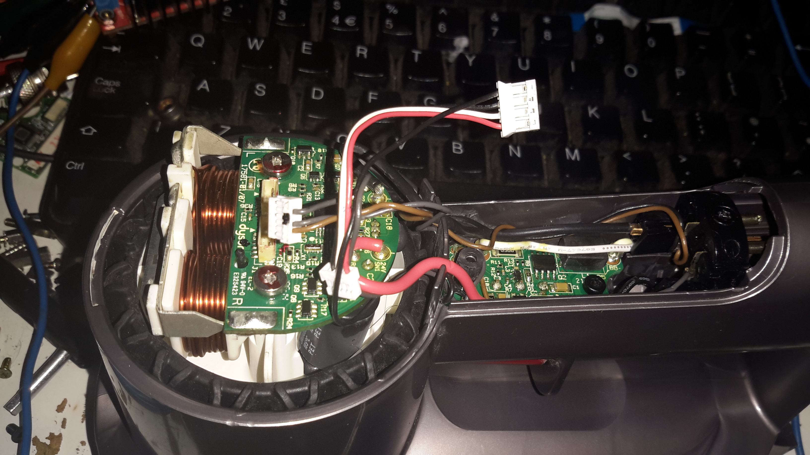
The inside face of the control PCB holds the 4 very large MOSFETs, IRFH7932PbF from International Rectifier. These are rated at 30v 20A a piece, and are probably wired in a H-Bridge. There’s a bipolar Hall switch to sense rotor position & rotation speed, and an enormous pair of capacitors on the main power bus.
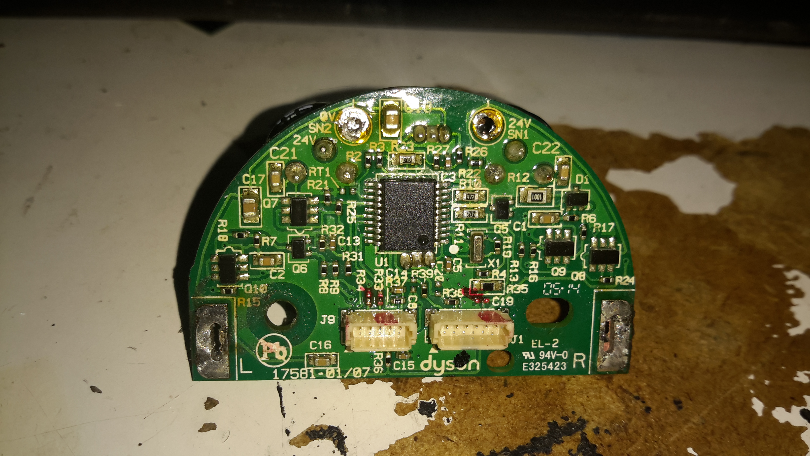
Not much on the other side of the PCB other than the microcontroller and associated gate drive stuff for the FETs.
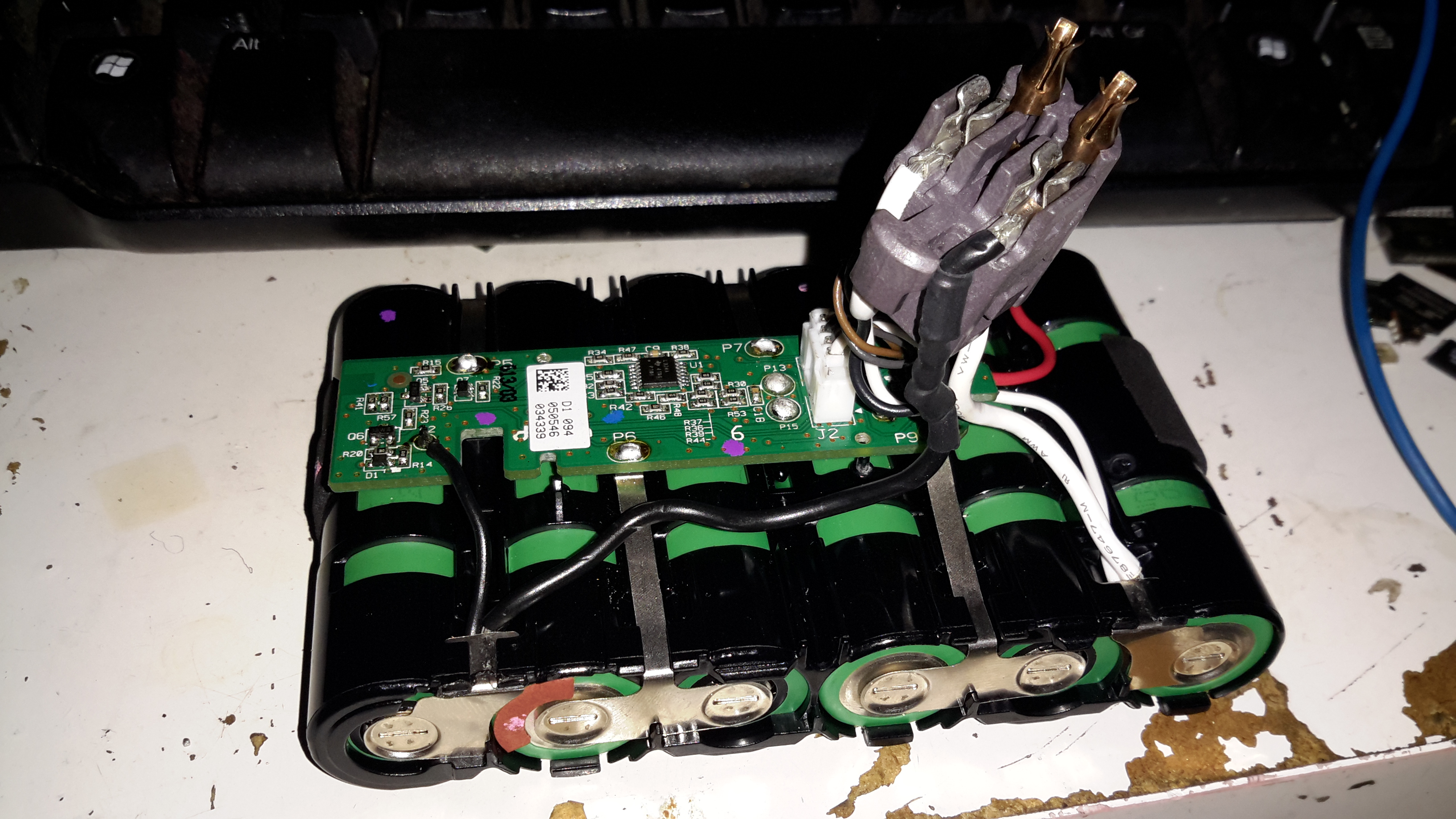
The battery pack is similar to the DC16 in it’s construction, a heavily clipped together plastic casing holding 6 lithium cells. In this one though there’s a full battery management system. The IC on the top of the board above is a quad Op-Amp, probably for measuring cell voltages.
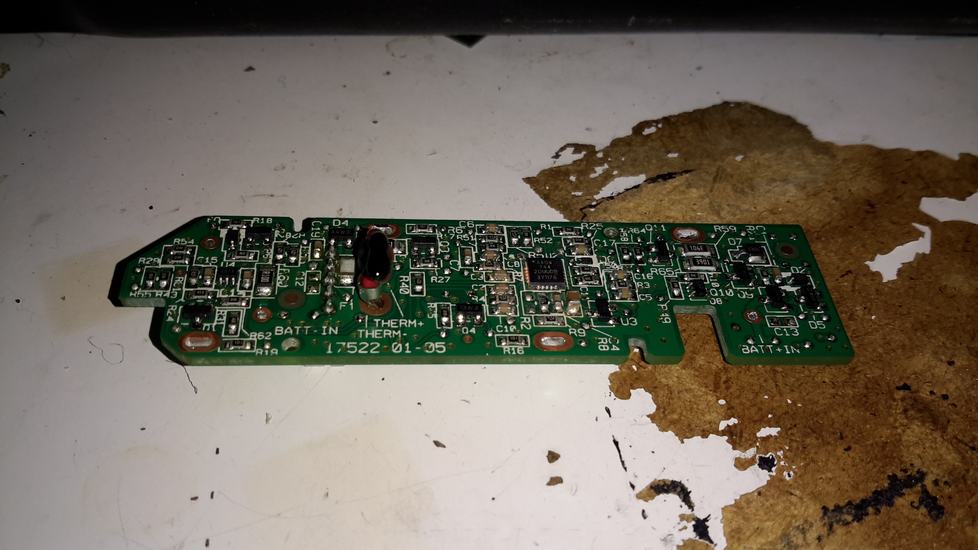
The other side of the BMS board is packed with components. I wasn’t able to identify the QFN IC here, as it’s got a custom part number, but it’s most definitely communicating with the main motor MCU via I²C over the two small terminals on the battery connector.