Posted on 5 Comments

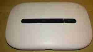
Vodafone Mobile WiFi R207 Teardown

Vodafone Mobile WiFi R207

Here’s one of the old modems from my spares bin, a Vodafone Mobile WiFi R207. This is just a rebranded Huawei E5330. This unit includes a 3G modem, and a WiFi chipset, running firmware that makes this a mini-router, with NAT.
Specs
Specs

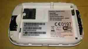
The back has the batter compartment & the SIM slot, with a large label showing all the important details.
Cover Removed
Cover Removed

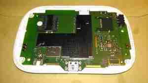
A couple of small Torx screws later & the shell splits in half. All the electronics are covered by shields here, but luckily they are the clip-on type, and aren’t soldered direct to the PCB.
Chipset
Chipset

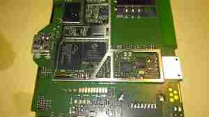
Once the shield has been removed, the main chipset is visible underneath. There’s a large Spansion MS01G200BHI00 1GBit flash, which is holding the firmware. Next to that is the Hi6758M baseband processor. This has all the hardware required to implement a 3G modem. Just to the right is a Hi6521 power management IC, which is dealing with all the power supplies needed by the CPU.
The RF section is above the baseband processor, some of which is hiding under the bits of the shield that aren’t removable.
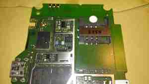
SIM Socket
SIM Socket

There’s a socket onboard for a standard Mini-SIM, just to the left of that is a Hi6561 4-phase buck converter. I would imagine this is providing the power supplies for the RF section & amplifier.
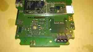
Unpopulated Parts
Unpopulated Parts

Not sure what this section is for, all the parts are unpopulated. Maybe a bluetooth option?
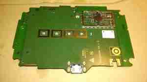
PCB Reverse
PCB Reverse

The other side of the PCB is pretty sparse, holding just the indicator LEDS, button & the WiFi Chipset.
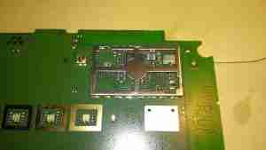
Realtek WiFi Chipset

The chipset here is a Realtek part, but it’s number is hidden by some of the shield. The antenna connection is routed to the edge of the board, where a spring terminal on the plastic case mounted antenna makes contact.
Posted on Leave a comment

Anker PowerPort Speed 5 12v DC Conversion

A few months ago I did a teardown on this Anker PowerPort Speed 5 USB charger, but I didn’t get round to detailing the conversion to 12v I had to do, so I’ll get to that now I’ve got a couple more to convert over.

Power Module
Power Module

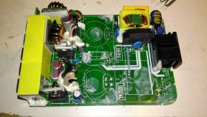
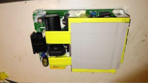
Here’s the internals of the Anker charger once I’ve removed the casing – which like many things these days, is glued together. (Joints can be cracked with a screwdriver handle without damaging the case). There’s lots of heatsinking in here to cool the primary side switching devices & the pot core transformers, so this is the first thing to get removed.

Heatsink Removed
Heatsink Removed

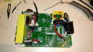
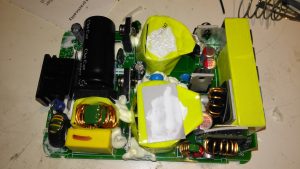
Once the heatsink has been removed, the pot core transformers are visible, wrapped in yellow tape. There’s some more heatsink pads & thermal grease here, to conduct heat better. The transformers, primary side switching components & input filter capacitor have to go.

Primary Side Components Removed

Here’s the PCB once all the now redundant mains conversion components have been deleted. I’ve left the input filtering & bridge rectifier in place, as this solves the issue of the figure-8 cable on the input being reversible, polarity of the input doesn’t matter with the bridge. I’ve removed the main filter capacitor to make enough room for the DC-DC converters to be fitted.

Tails Installed
Tails Installed

Installing the tails to connect everything together is the next step, this charger requires two power supplies – the QC3 circuits need 14.4v to supply the multi-voltage modules, the remaining 3 standard ports require 5v. The DC input tails are soldered into place where the main filter capacitor was, while the outputs are fitted to the spot the transformer secondary windings ended up. I’ve left the factory Schottky rectifiers in place on the secondary side to make things a little more simple, the output voltages of both the DC-DC converters does need to be increased slightly to compensate for the diode drops though. I’ve also bypassed the mains input fuse, as at 12v the input current is going to be substantially higher than when used on mains voltage.

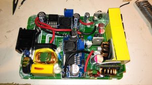
DC-DC Converters Installed

With a squeeze both the boost converter & the buck converter fit into place on the PCB.

Posted on Leave a comment

Philips LED PAR38 Lamp Teardown

Philips PAR38
Philips PAR38

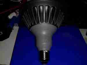
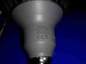
These large LED Philips PAR38 lamps were recently on clearance sale in my local T.N. Robinsons electrical contractors for about £3, so I decided to grab one in the hopes I might be able to hack it into a low-voltage LED lamp. These are full-size PAR38 format, with most of the bulk being the large aluminium heatsink on the front. The back section with the power supply module is secured with silicone, so some unreasonable force was required to liberate the two pieces.

Specification
Specification

These lamps are rated at 18W in operation, and are surprisingly bright for this power level.

Lens
Lens

The front has the moulded multi-lens over the LEDs, to spread the light a bit further than the bare dies.

LED Array
LED Array

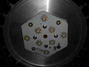
The LED array is two series strings of 4 LEDs, for ~24v forward voltage. Unusual for a high power LED array, this PCB isn’t aluminium cored, but 0.8mm FR4. Heat is transferred to the copper plane on the backside by the dozens of vias around the Luxeon Rebel LEDs. There is a thermal pad under the PCB for improved heat transfer to the machined surface of the heatsink.

Control PCB Top
Control PCB Top

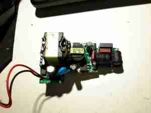
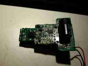
The power supply & control PCB is pretty well made, it’s an isolated converter, so no nasty mains on the LED connections.

Control PCB Bottom
Control PCB Bottom
Posted on Leave a comment

Maplin 3W LED Torch Charger Fail

A member of the family recently bought one of these torches from Maplin electronics, and the included chargers for the 18650 lithium-ion cells leave a lot to be desired.

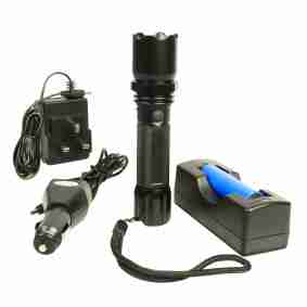
Torch
Torch

Here’s what’s supplied. The torch itself is OK – very bright, and a good size. Me being cynical of overpriced Chinese equipment with lithium batteries, I decided to look in the charging base & the cigar-lighter adaptor to see if there was any actual charging logic.

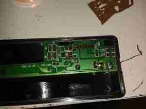
Charger
Charger

Answer – nope. Not a single active component in here. It’s just a jack connected to the battery terminals. There’s all the space there to fit a proper charging circuit, but it’s been left out to save money.

OK then, is it inside the cigarette lighter adaptor?

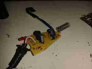
Lighter Adaptor
Lighter Adaptor

Nope. Not a single sign of anything resembling a Lithium-Ion charger IC. There’s a standard MC34063A 1.5A Buck converter IC on the bottom of the PCB, this is what’s giving the low voltage output for the torch.

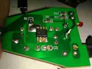
Charger Bottom
Charger Bottom

Here’s the IC – just a buck converter. The output voltage here is 4.3v. This is higher than the safe charging voltage of a lithium ion cell, of 4.2v.

The cells supplied are “protected” versions, having charge/discharge protection circuitry built onto the end of the cell on a small PCB, this makes the cell slightly longer than a bare 18650, so it’s easy to tell them apart.
The manufacturers in this case are relying on that protection circuit on the cell to prevent an overcharge condition – this isn’t the purpose they’re designed for, and charging this way is very stressful for the cells. I wouldn’t like to leave one of these units charging unattended, as a battery explosion might result.

More to come shortly when I build a proper charger for this torch, so it can be recharged without fearing an alkali metal fire!

73s for now folks!

Posted on Leave a comment

He-Ne Laser

He-Ne Laser Mount
He-Ne Laser Mount

Having had a He-Ne laser tube for a while & the required power supply, it was time to mount the tube in a more sturdy manner. Above the tube is mounted with a pair of 32mm Terry Clips, with the power leads passing through the plastic top. The ballast resistor is built into the silicone rubber on the anode end of the tube. (Right).
Output power is about 1mW for this tube, which came from a supermarket barcode scanner from the 90’s. The tube is dated August 1993 & is manufactured by Aerotech.

Internals
Internals

Inside the box is the usual 2.2Ah 12v Li-Po battery pack & the brick type He-Ne laser supply. The small circuit in the centre is a switchmode converter that drops the 12v from the battery pack to the 5v required for the laser supply.

Posted on 1 Comment

MSR605 3-Track Magnetic Stripe Writer

MSR605
MSR605

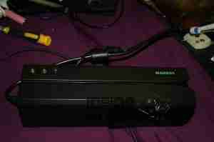
This unit was bought from eBay to experiment with Magnetic Stripe cards, for little money. This unit is capable of reading & writing all 3 tracks, & both Hi-Co & Lo-Co card types.
Interfaced to a PC through USB, this has a built in PL2303 USB-Serial IC & requires 3A at 9v DC to operate.
The 3 Indicator LEDs on the top of the unit can be toggled by the included software for Power/OK/Fault condition signalling.

Unit Bottom
Unit Bottom

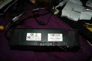
Bottom of the unit with the model labels.

Model Label
Model Label

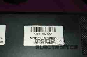
Closeup of the model label & serial number.

PCB Bottom
PCB Bottom

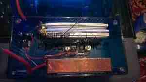
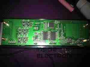
Here the bottom cover has been removed, showing the main PCB. The pair of large ICs bottom center interface with the magnetic heads. The IC above them has had the markings sanded off.

USB-Serial Interface

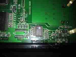
Closeup of the Prolific PL-2303 USB-Serial converter IC.

PCB Top
PCB Top

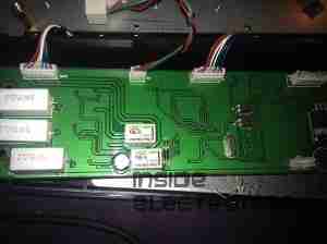
Here the connections to the R/W heads are visible, current limiting resistors at the left for the write head, a pair of signal relays, a pair of optoisolators & a LM7805 linear voltage regulator.

LEDs
LEDs

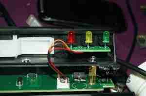
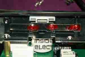
Here is the trio of indicator LEDs on a small sub-board.

Frame Bottom
Frame Bottom

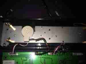
The PCB has been removed from the main frame here, the only component visible is the rotary encoder.

Rotary Encoder
Rotary Encoder

The rotary encoder has a rubber wheel fitted, which reads the speed of the card as it is being swiped for writing. This allows the control logic to write the data to the stripe at the correct rate for the speed of the card. This allows the unit to write cards from 5-50 inches per second speed.
The Write head is directly behind the rubber pressure roller.

Read/Write Heads
Read/Write Heads

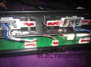
Here you can see the R/W head assembly. The write head is on the right, read on the left. When a card is written to, it immediately gets read by the second head for verification.

The drivers for this unit are also available here: Magcard Writer Drivers

Posted on Leave a comment

USB-IDE/SATA Adaptor

Front
Front

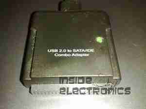
This is a device to use an IDE or SATA interface drive via a USB connection. Here is the front of the device, IDE interface at the bottom, 2.5″ form factor.

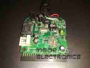
PCB Top
PCB Top

PCB removed from the casing. USB cable exits the top, 12v DC power jack to the left.
SATA interface below the DC Jack.
Molex connector below SATA is the power output for the drive in use. This unit has a built in 5v regulator.

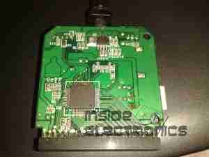
PCB Bottom
PCB Bottom

Bottom of the PCB showing the interface IC.

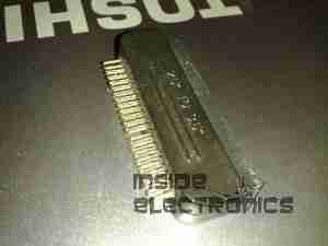
Drive Adaptor
Drive Adaptor

Adaptor to plug into the 44-pin 2.5″ form factor IDE interface on the adaptor, converts to standard 40-pin 3.5″ IDE.

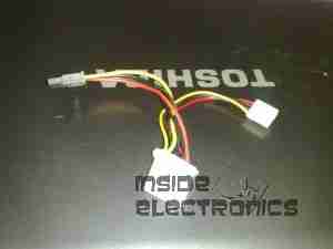
Power Cable
Power Cable

Power pigtail with standard Molex & SATA power plugs.