![Front Front](http://www.experimental-engineering.co.uk/wp-content/uploads/2011/01/GEDC0622-Comp-300x225.jpg)
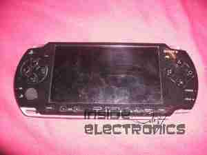
Here is a PSP Slim that recently died.
![Label Label](http://www.experimental-engineering.co.uk/wp-content/uploads/2011/01/GEDC0626-Comp-300x225.jpg)
For those that are interested, here is the ID label, this is a PSP-2003.
![Front Removed Front Removed](http://www.experimental-engineering.co.uk/wp-content/uploads/2011/01/GEDC0631-Comp-300x225.jpg)
Here the front of the unit has been removed, showing the first internal components.
![Screen Removed Screen Removed](http://www.experimental-engineering.co.uk/wp-content/uploads/2011/01/GEDC0639-Comp-300x225.jpg)
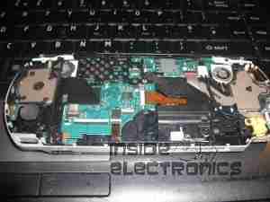
Here is the unit with the LCD removed, here the mainboard is partially visible.
![Left Pad Left Pad](http://www.experimental-engineering.co.uk/wp-content/uploads/2011/01/GEDC0642-Comp-300x225.jpg)
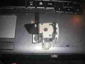
Left pad unit removed from the PSP, with the left speaker & the memory stick slot cover.
![Left Pad Rear Left Pad Rear](http://www.experimental-engineering.co.uk/wp-content/uploads/2011/01/GEDC0640-300x225.jpg)
Rear of the left pad assembly, showing the speaker.
![Joypad Joypad](http://www.experimental-engineering.co.uk/wp-content/uploads/2011/01/GEDC0665-300x225.jpg)
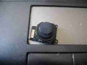
Joypad removed from the casing. Resistive unit.
![Output Jack Output Jack](http://www.experimental-engineering.co.uk/wp-content/uploads/2011/01/GEDC0666-300x225.jpg)
Headphone/data board removed from the casing. This also has TV-Out on the PSP-200x series.
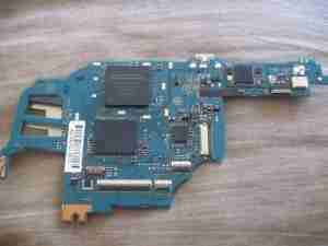
![Mainboard Mainboard](http://www.experimental-engineering.co.uk/wp-content/uploads/2011/01/GEDC0657-300x225.jpg)
Mainboard removed. Main CPU is at the top. Sockets around the bottom connect to the UMD drive & UMD Drive.
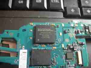
![CPU & GPU CPU & GPU](http://www.experimental-engineering.co.uk/wp-content/uploads/2011/01/GEDC0645-300x225.jpg)
Closeup of the main chipset. CPU is the top IC.
![Mainboard Rear Mainboard Rear](http://www.experimental-engineering.co.uk/wp-content/uploads/2011/01/GEDC0647-300x225.jpg)
Rear of the mainboard, Memory Stick socket on the right.
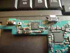
![WiFi Chipset WiFi Chipset](http://www.experimental-engineering.co.uk/wp-content/uploads/2011/01/GEDC0646-300x225.jpg)
Closeup of the WiFi chipset & the charging power socket on the right.
![Charging Chipset Charging Chipset](http://www.experimental-engineering.co.uk/wp-content/uploads/2011/01/GEDC0649-300x225.jpg)
Closeup of the bettery connector & the charge controller IC.
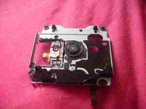
![UMD Drive UMD Drive](http://www.experimental-engineering.co.uk/wp-content/uploads/2011/01/GEDC0663-300x225.jpg)
UMD Drive removed from the rear of the casing. This is a miniature DVD style drive, using a 635nm visible red laser.
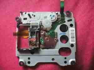
![UMD Drive Back UMD Drive Back](http://www.experimental-engineering.co.uk/wp-content/uploads/2011/01/GEDC0664-Comp-300x225.jpg)
Rear of the UMD drive, showing the laser sled & drive motors. Both the spindle motor & the sled motor are 3-phase brushless type. The laser diode/photodiode array is at the top of the laser sled.