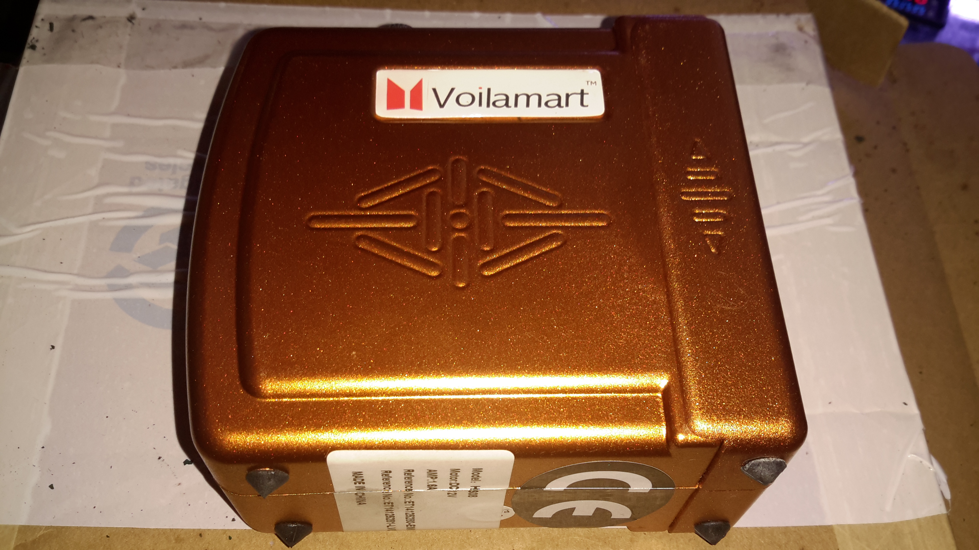
A while back I found myself in the need of an adjustable RF attenuator capable of high-GHz operation. As luck would have it I had an old Spectrum analyser on the shelf at work, which we had retired quite some time ago.
Spectrum analysers being quite capable test instruments, I knew that the input attenuation would be done with a standalone module that we could recover for reuse without too much trouble.
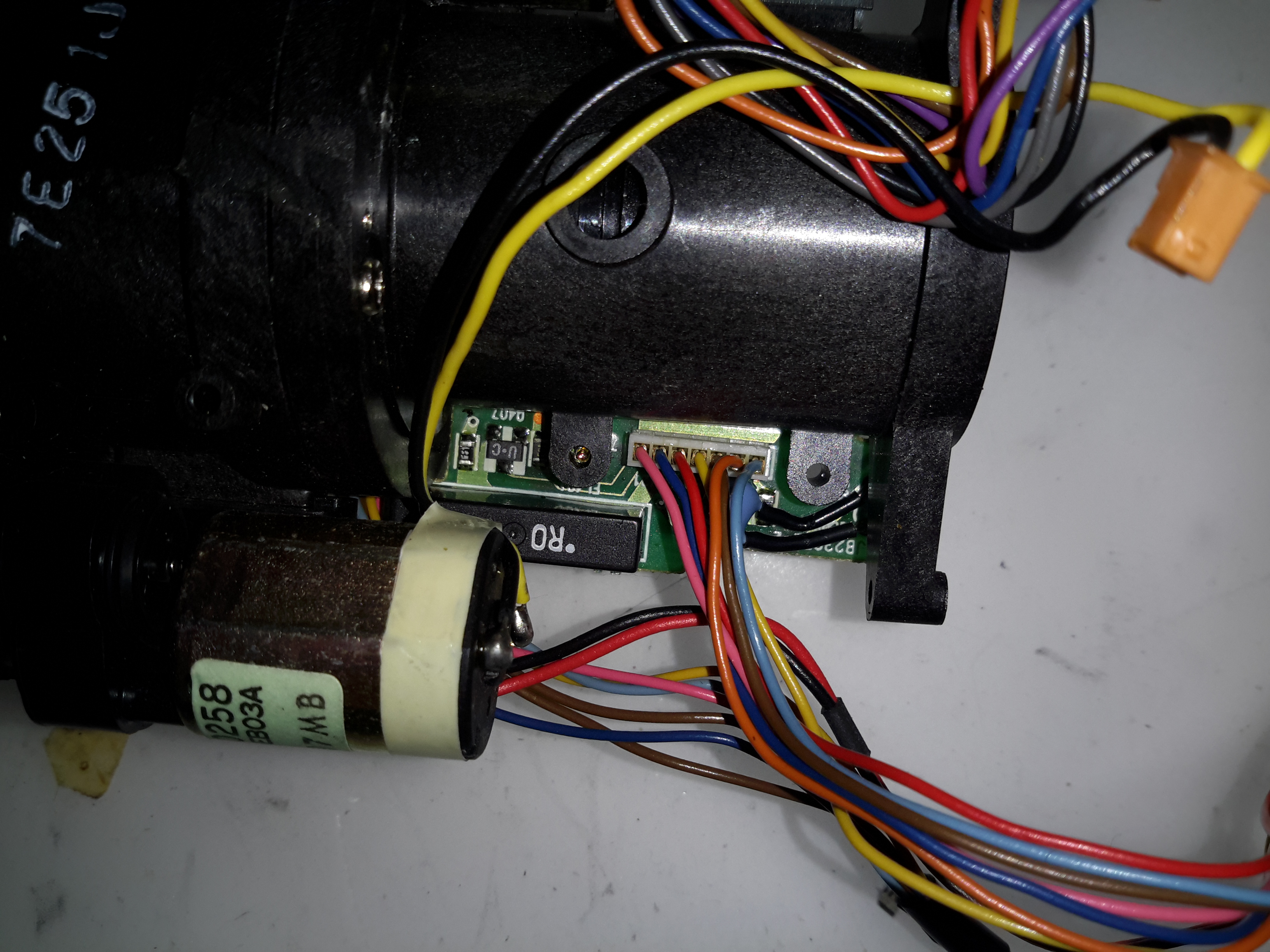
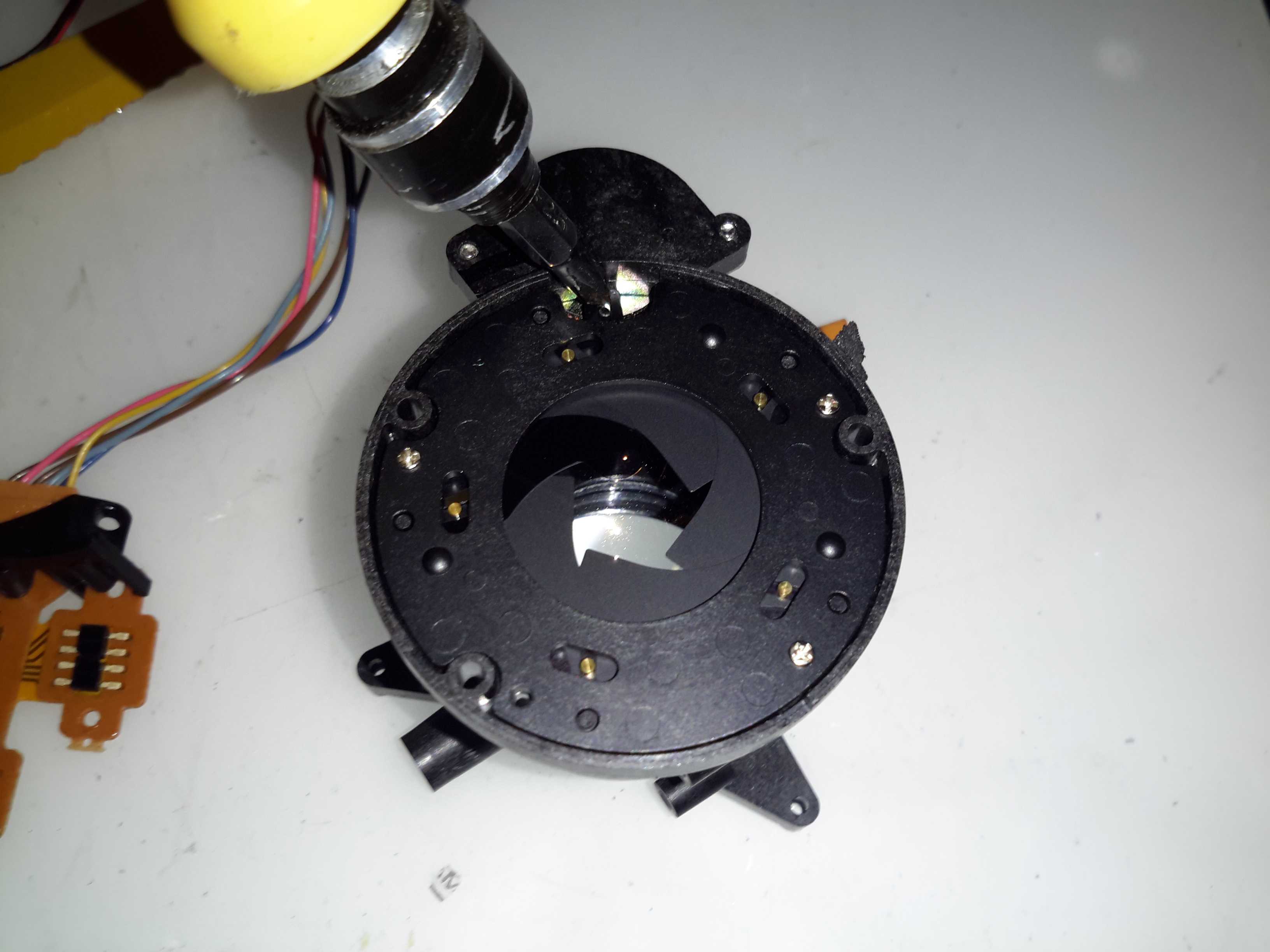
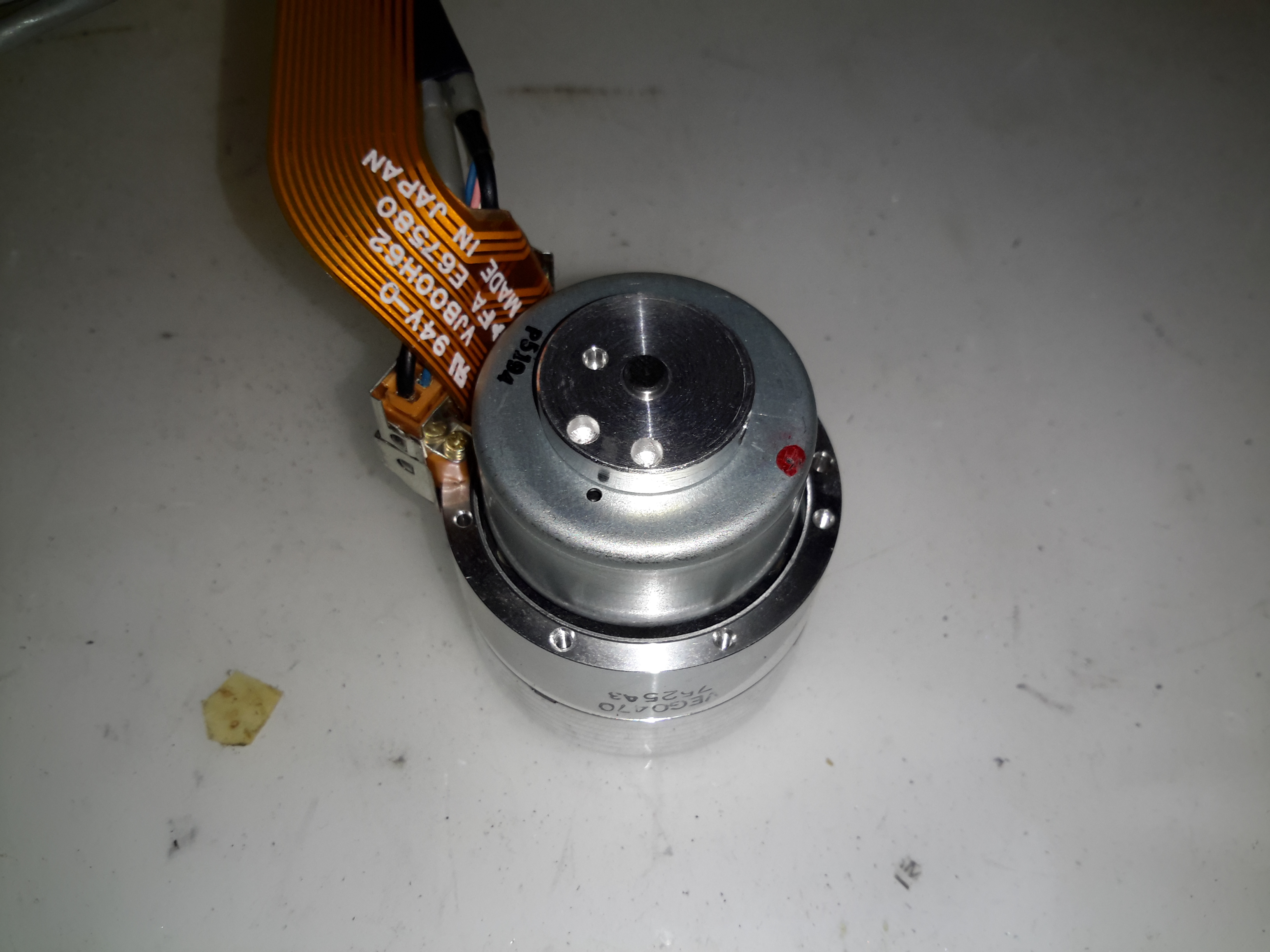
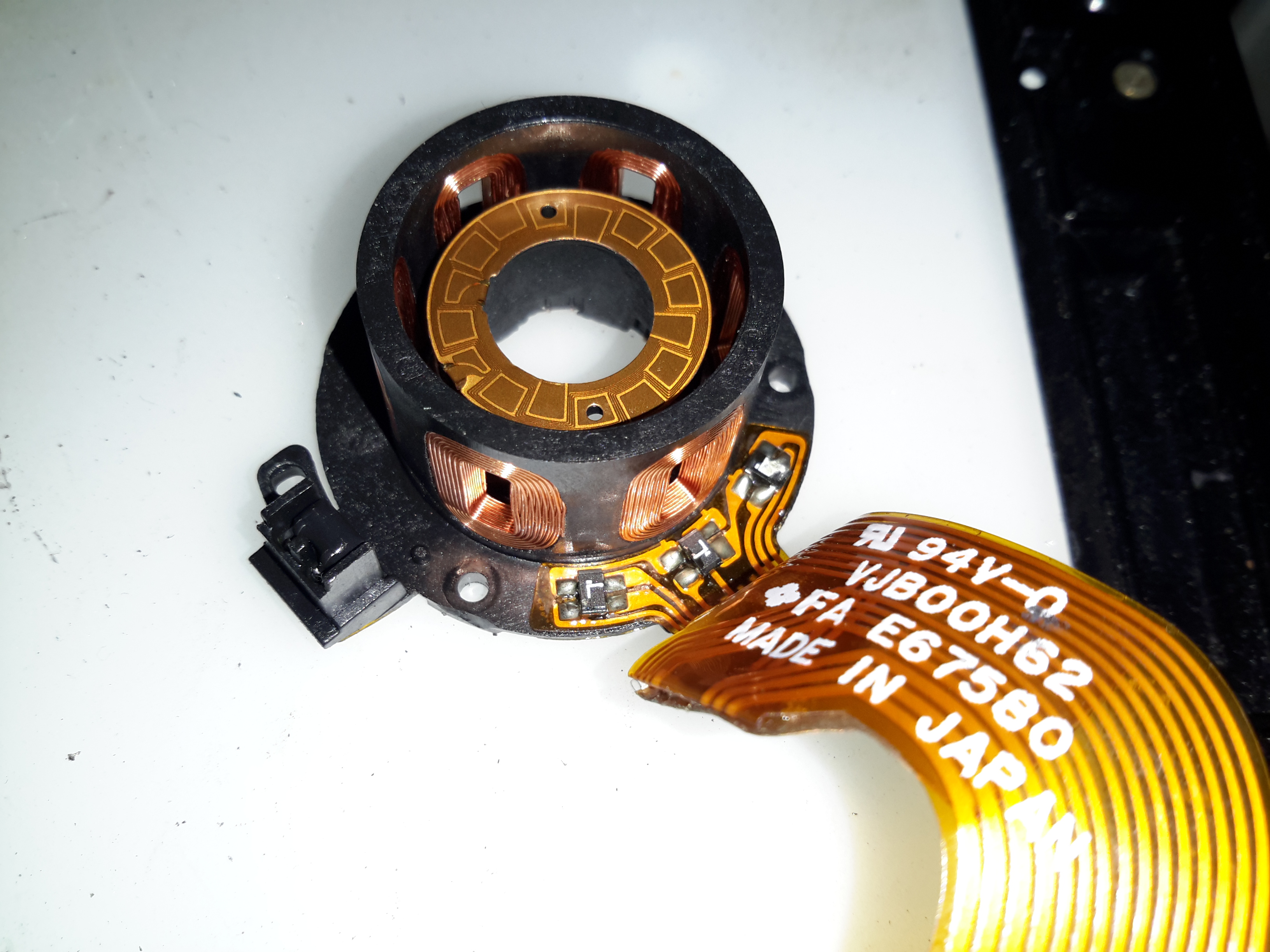
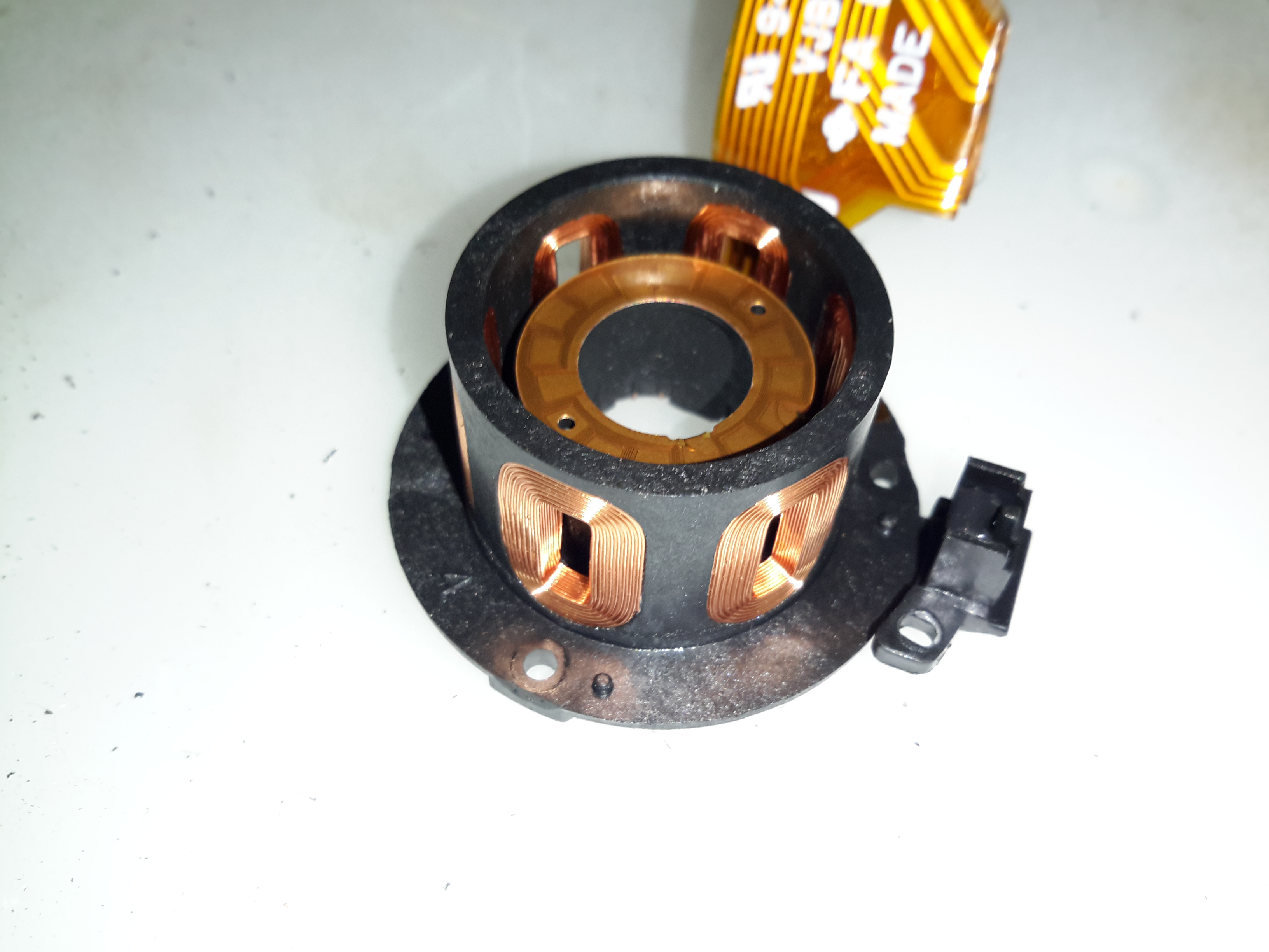
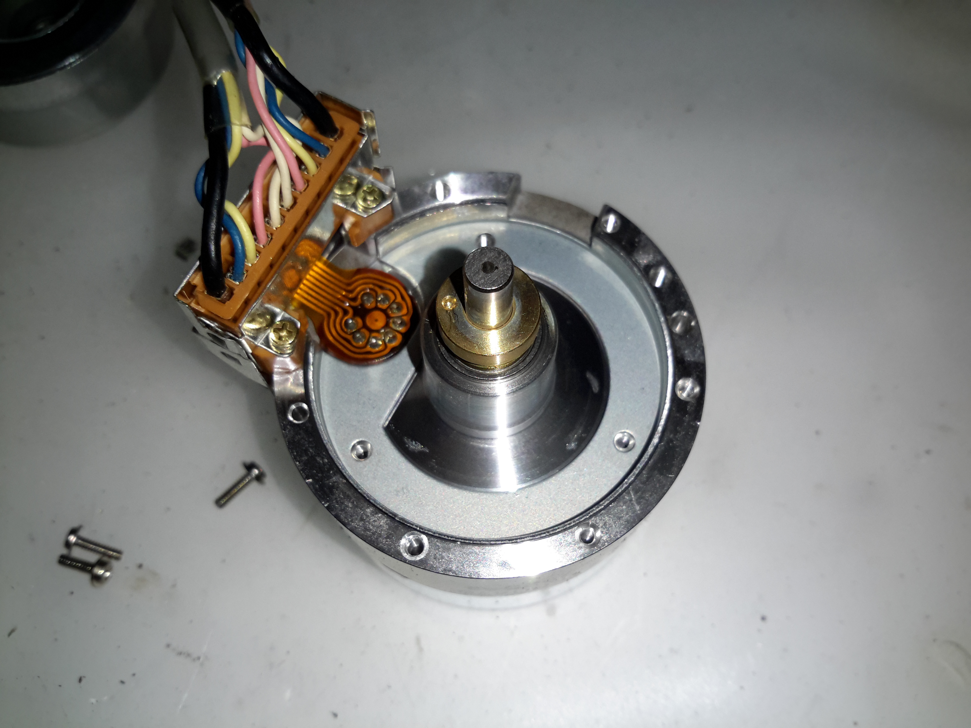
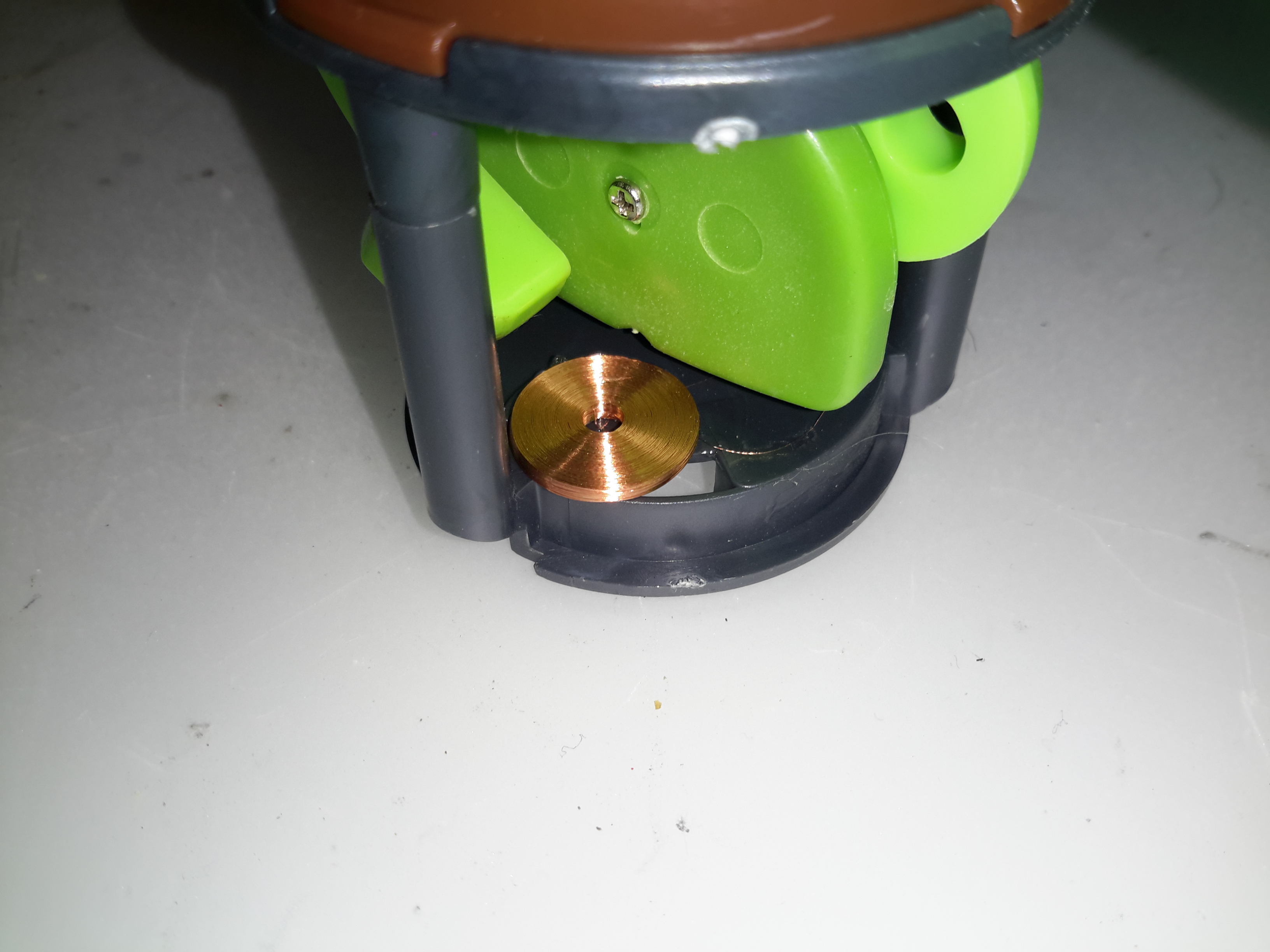
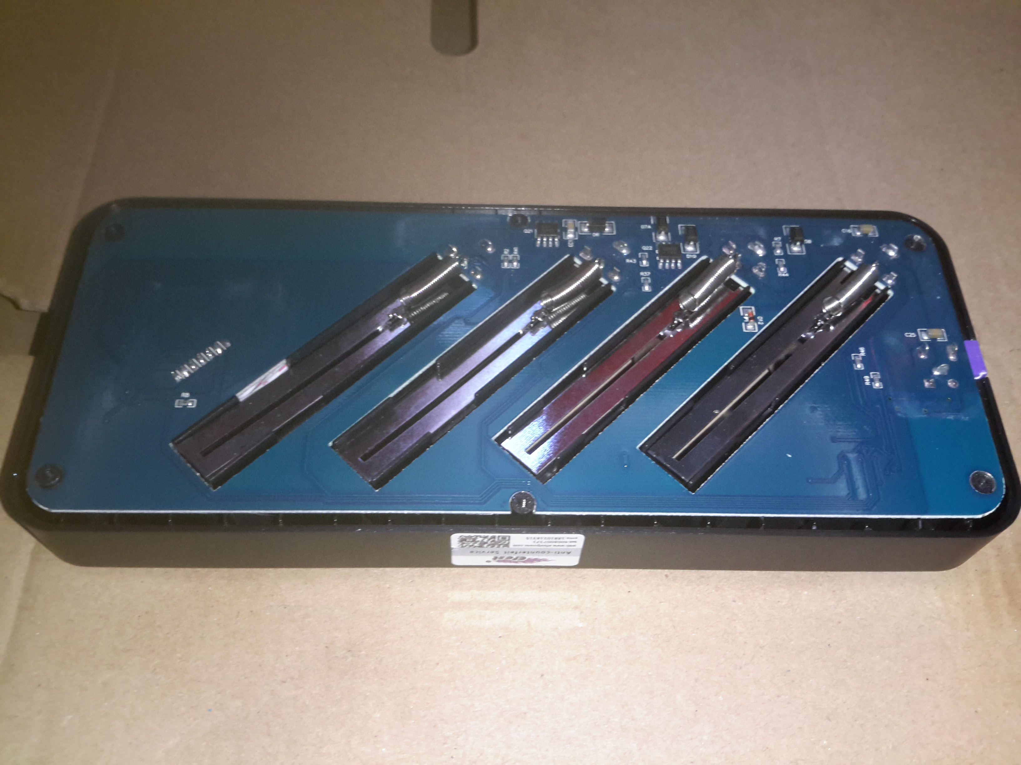
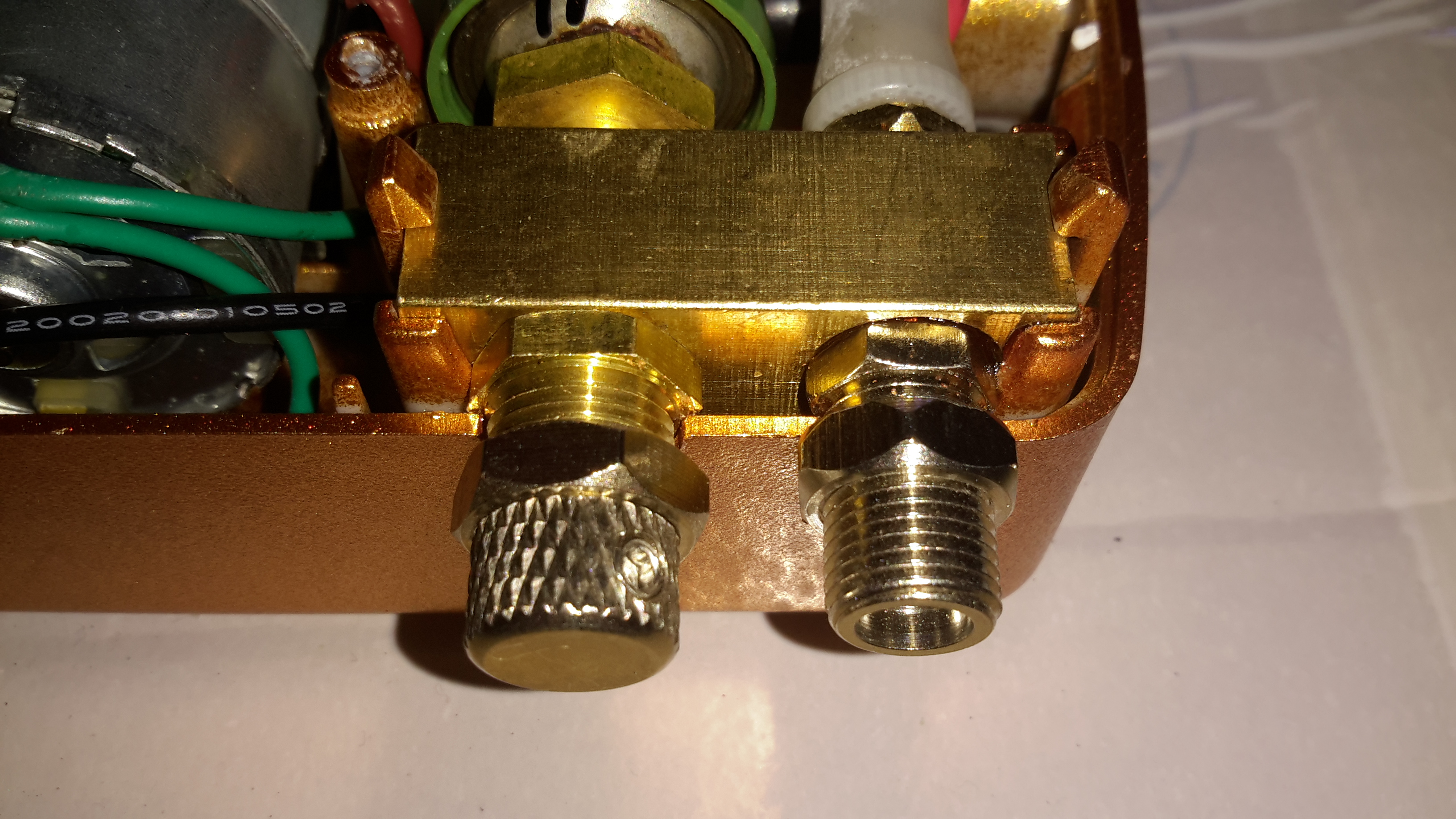
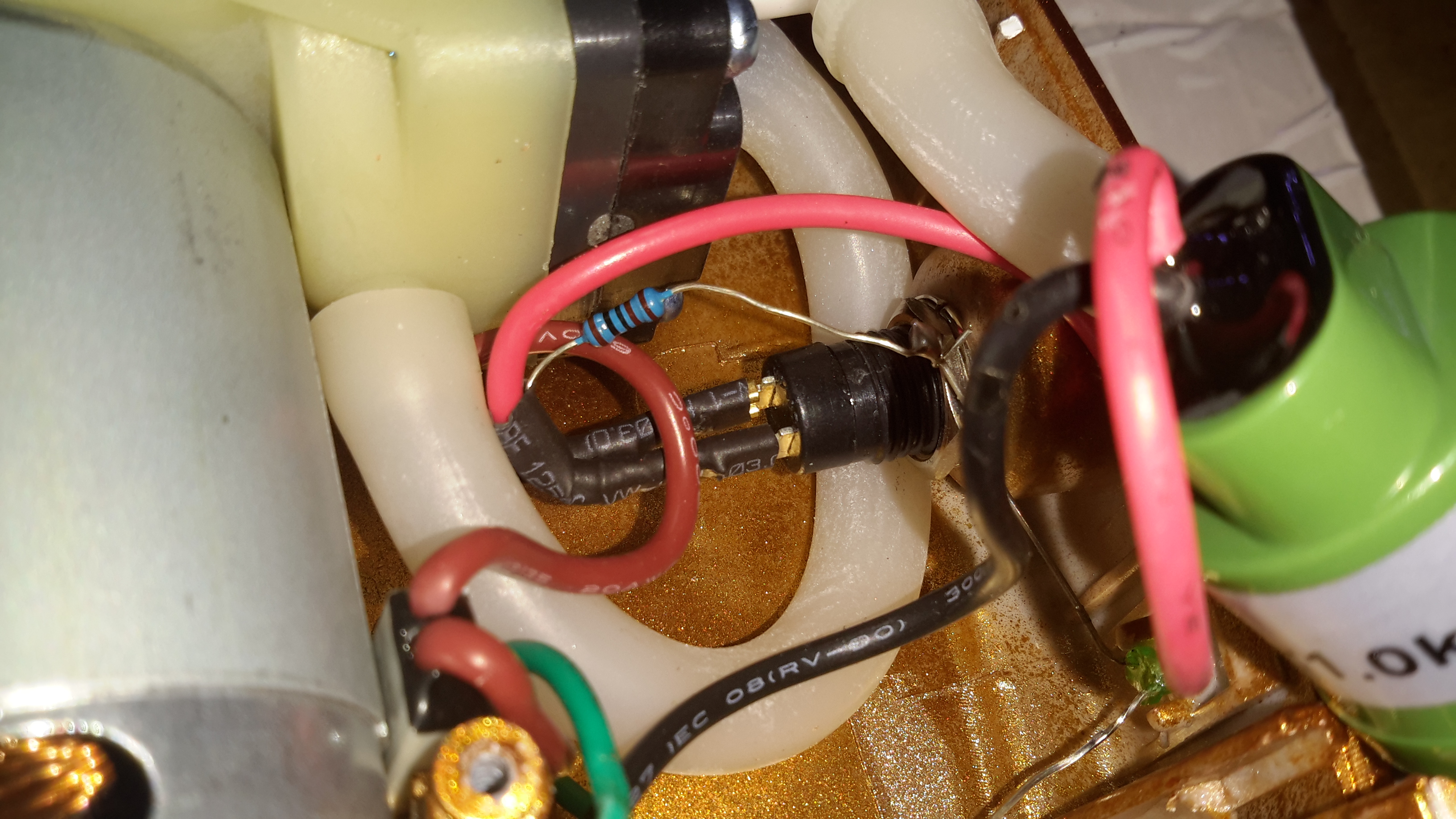
The attenuator module
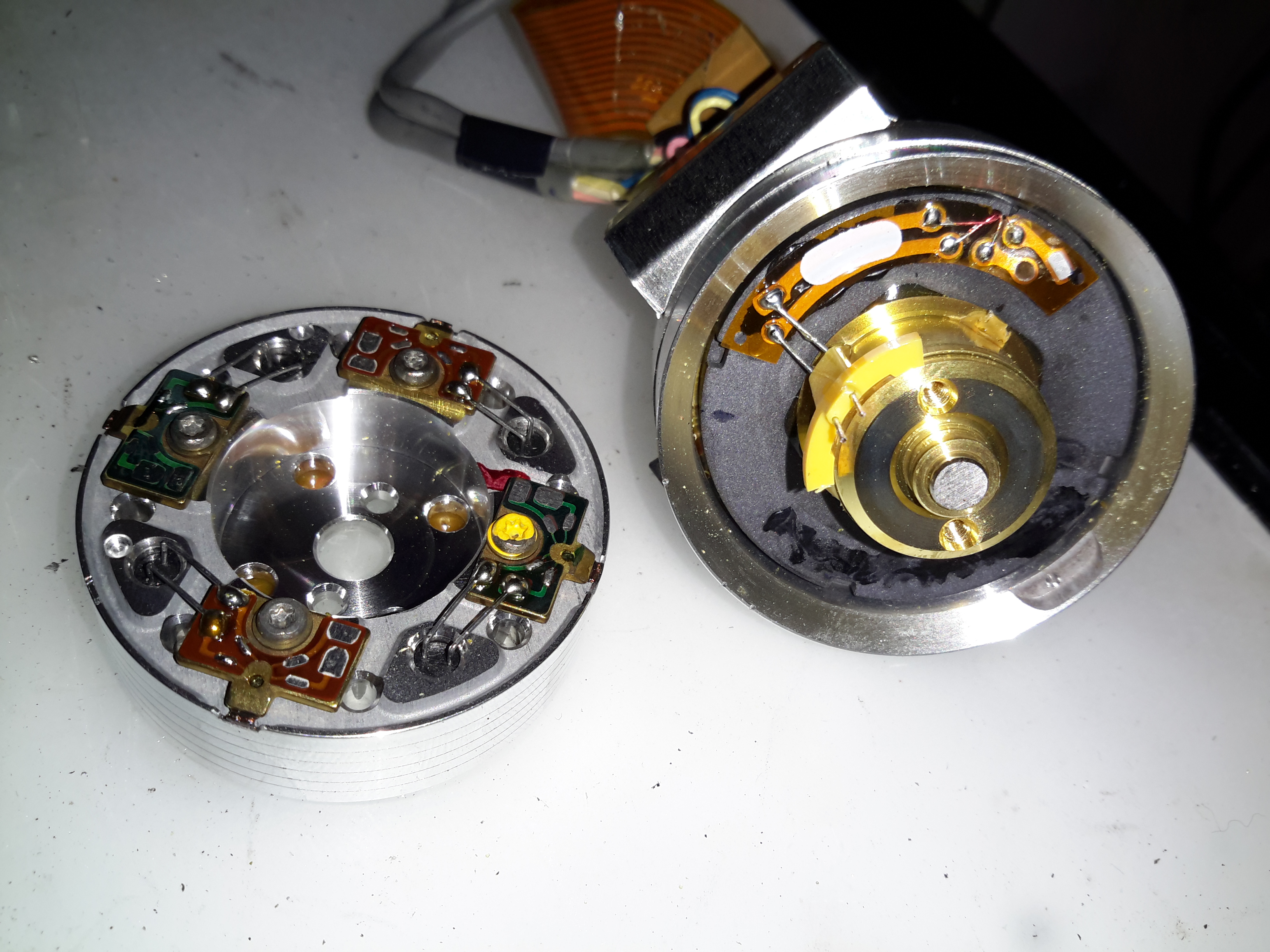
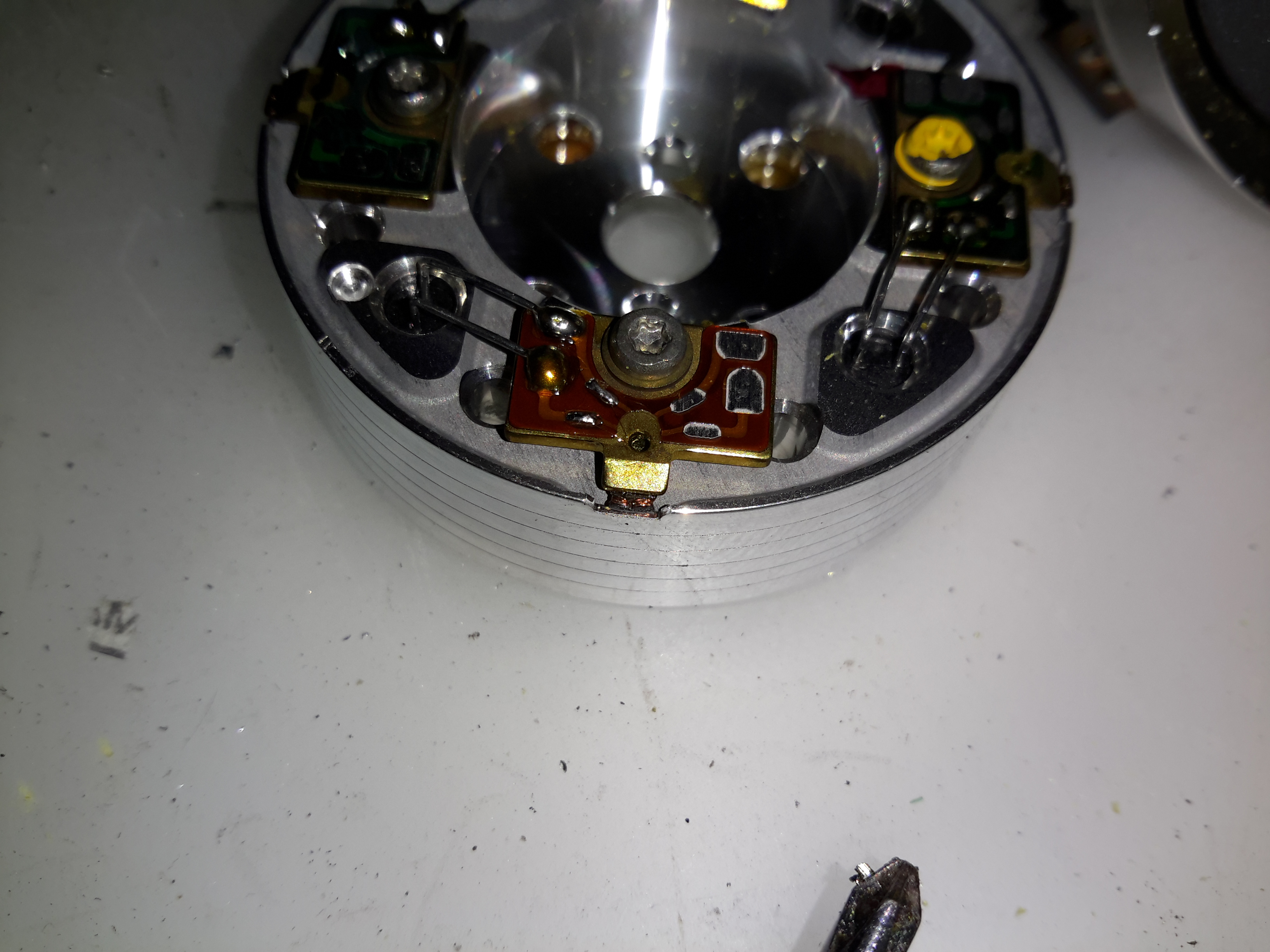
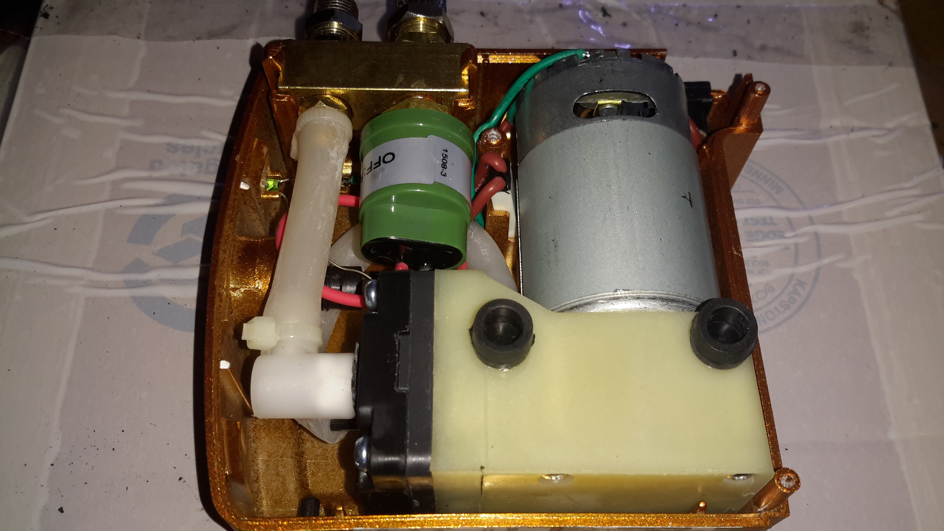
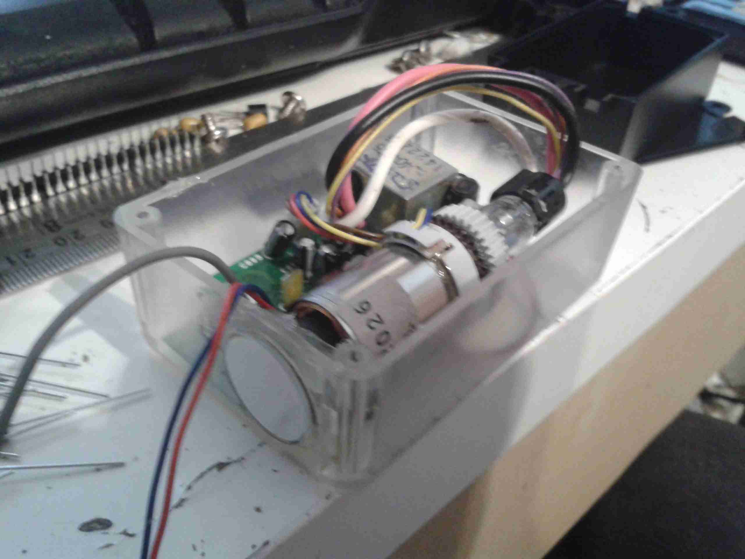
Here’s the module itself, with the factory drive PCB removed from the bottom, showing the solenoids that operate the RF switches. There are test wires attached to them here to work out which solenoid switches which attenuation stage. In the case of this module, there are switches for the following:
Input select switch
AC/DC coupling
-5dB
-10dB
-20dB
-40dB
For me this means I have up to -75dB attenuation in 5dB steps, with optional switchable A-B input & either AC or DC coupling.
Drive is easy, requiring a pulse on the solenoid coil to switch over, the polarity depending on which way the switch is going.
Building a Control Board
Now I’ve identified that the module was reusable, it was time to spin up a board to integrate all the features we needed:
Onboard battery power
Pushbutton operation
Indication of current attenuation level
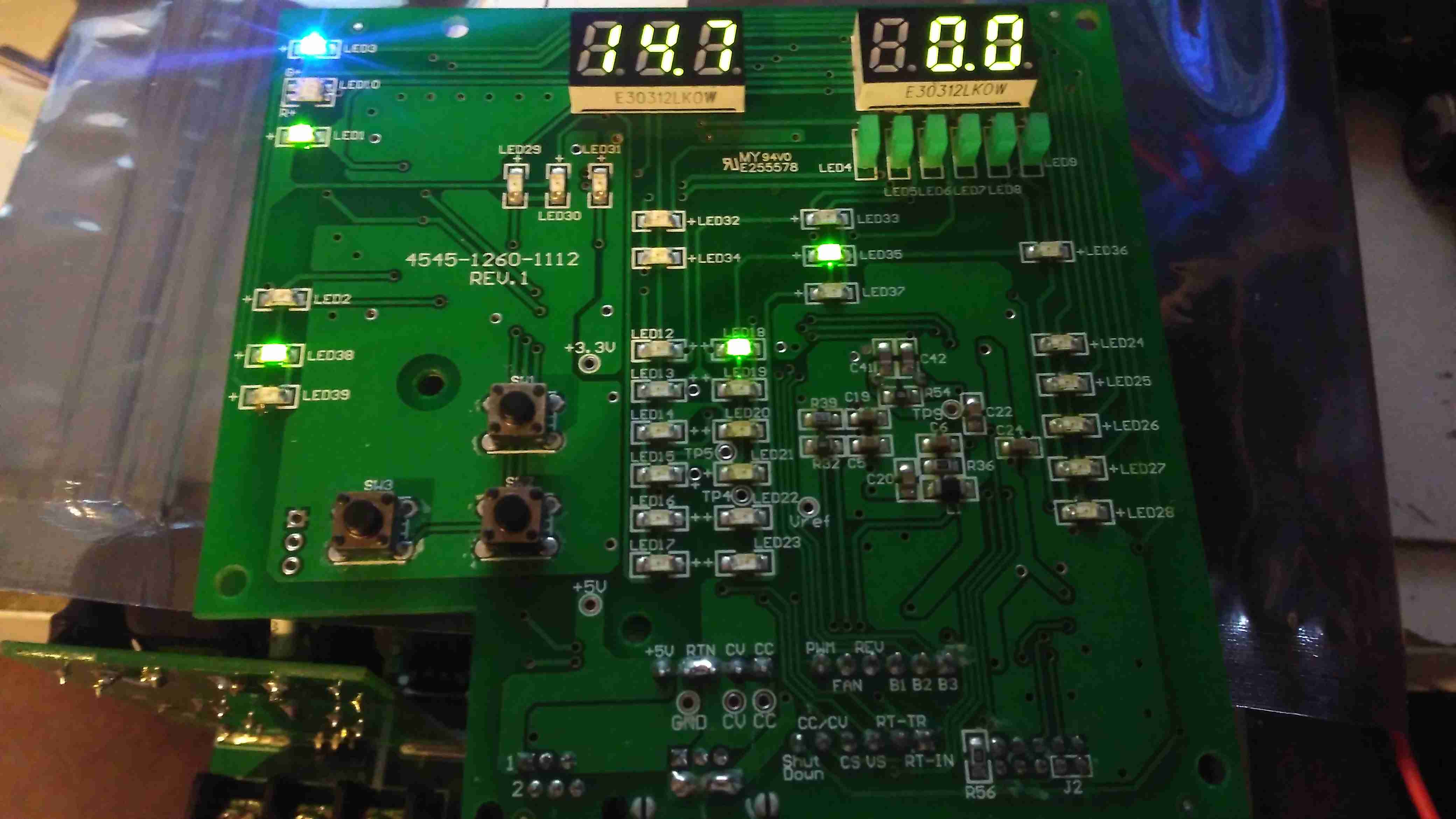
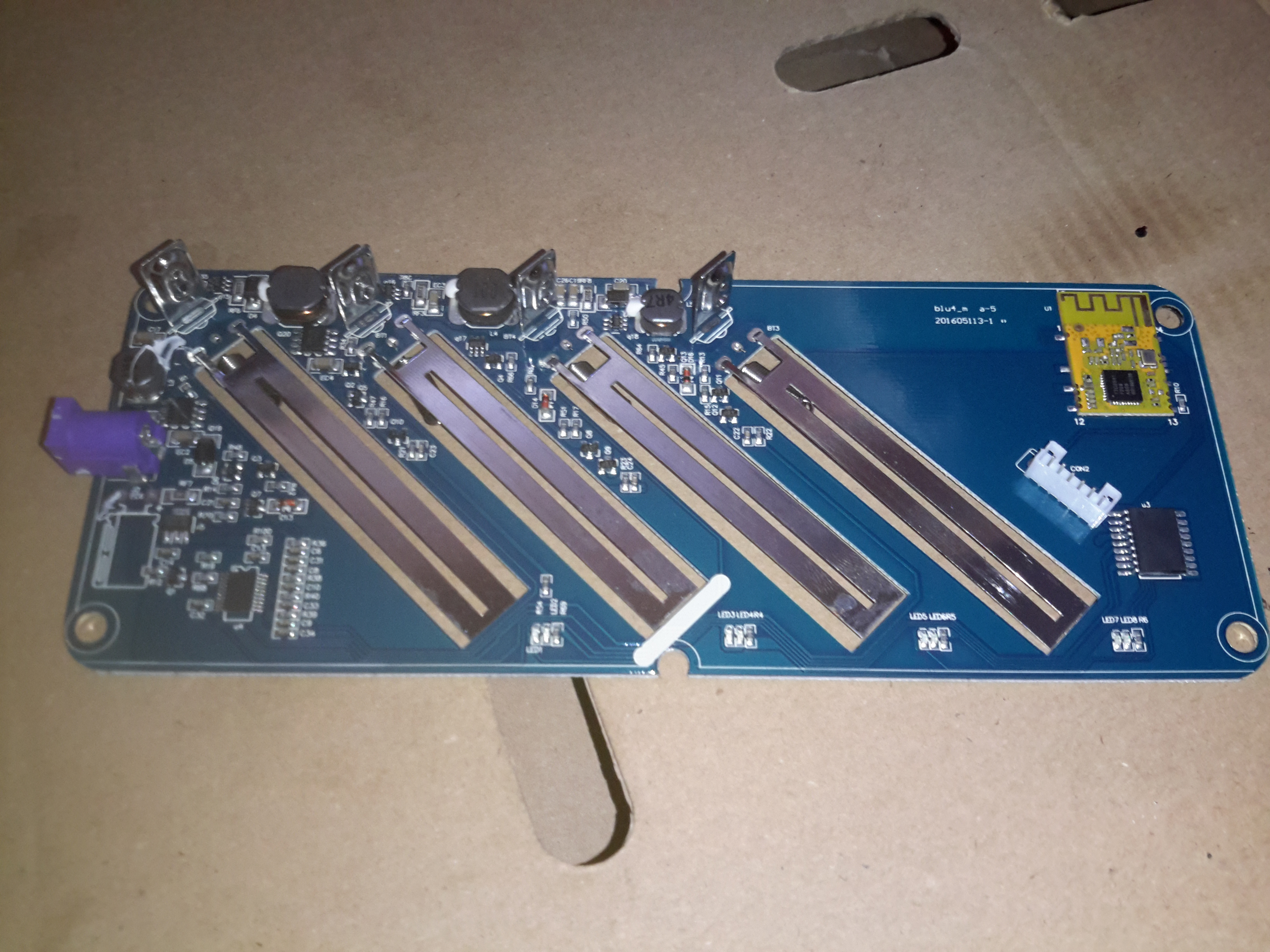
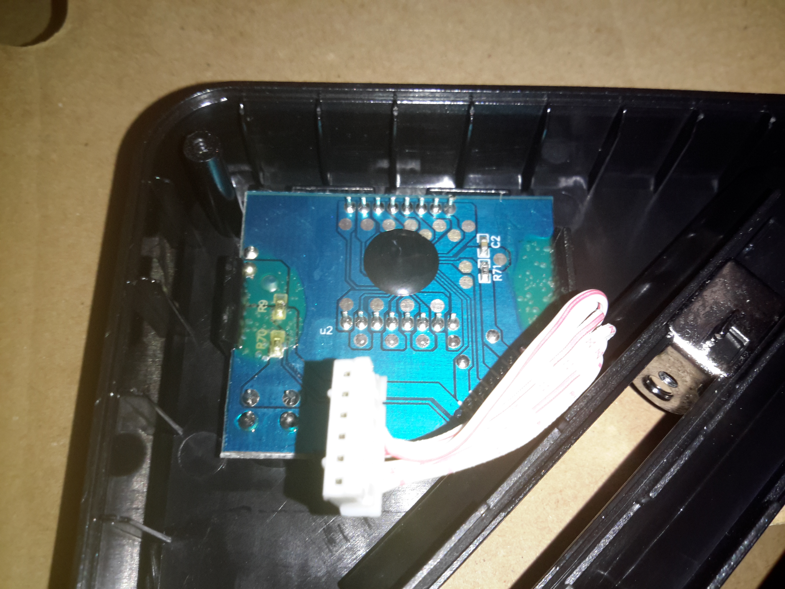
The partially populated board is shown at right, with an Arduino microcontroller for main control, 18650 battery socket on the right, and control buttons in the centre. The OLED display module for showing the current attenuation level & battery voltage level is missing at the moment, but it’s clear where this goes.
As there weren’t enough GPIO pins for everything on the Arduino, a Microchip MC23017 16-Bit I/O expander, which is controlled via an I²C bus. This is convenient since I’m already using I²C for the onboard display.
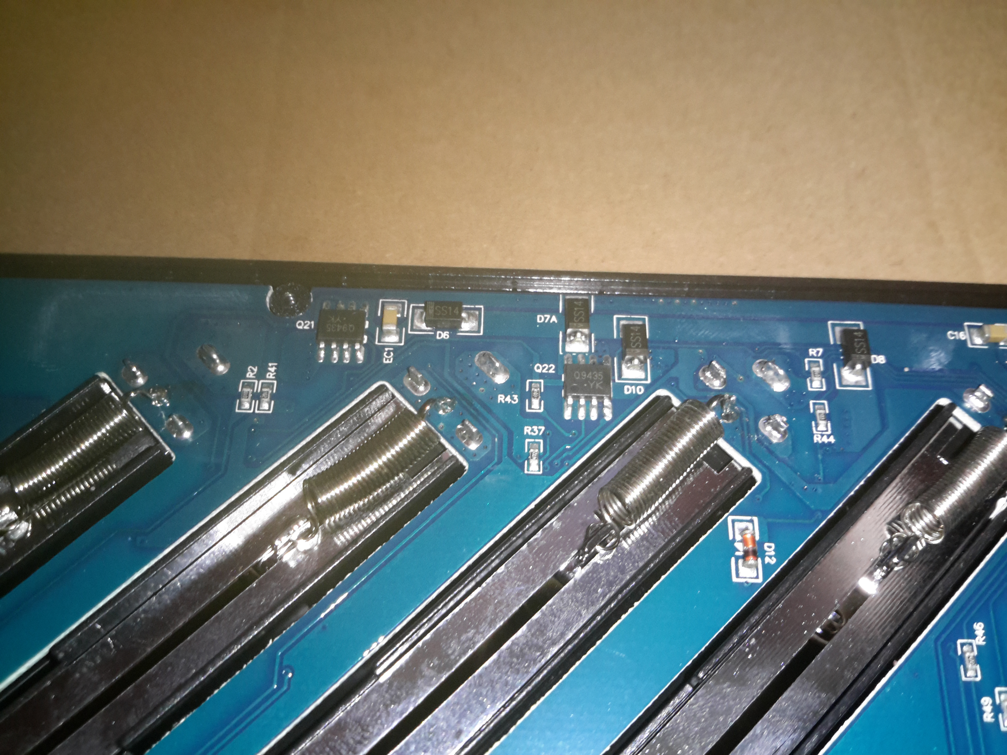
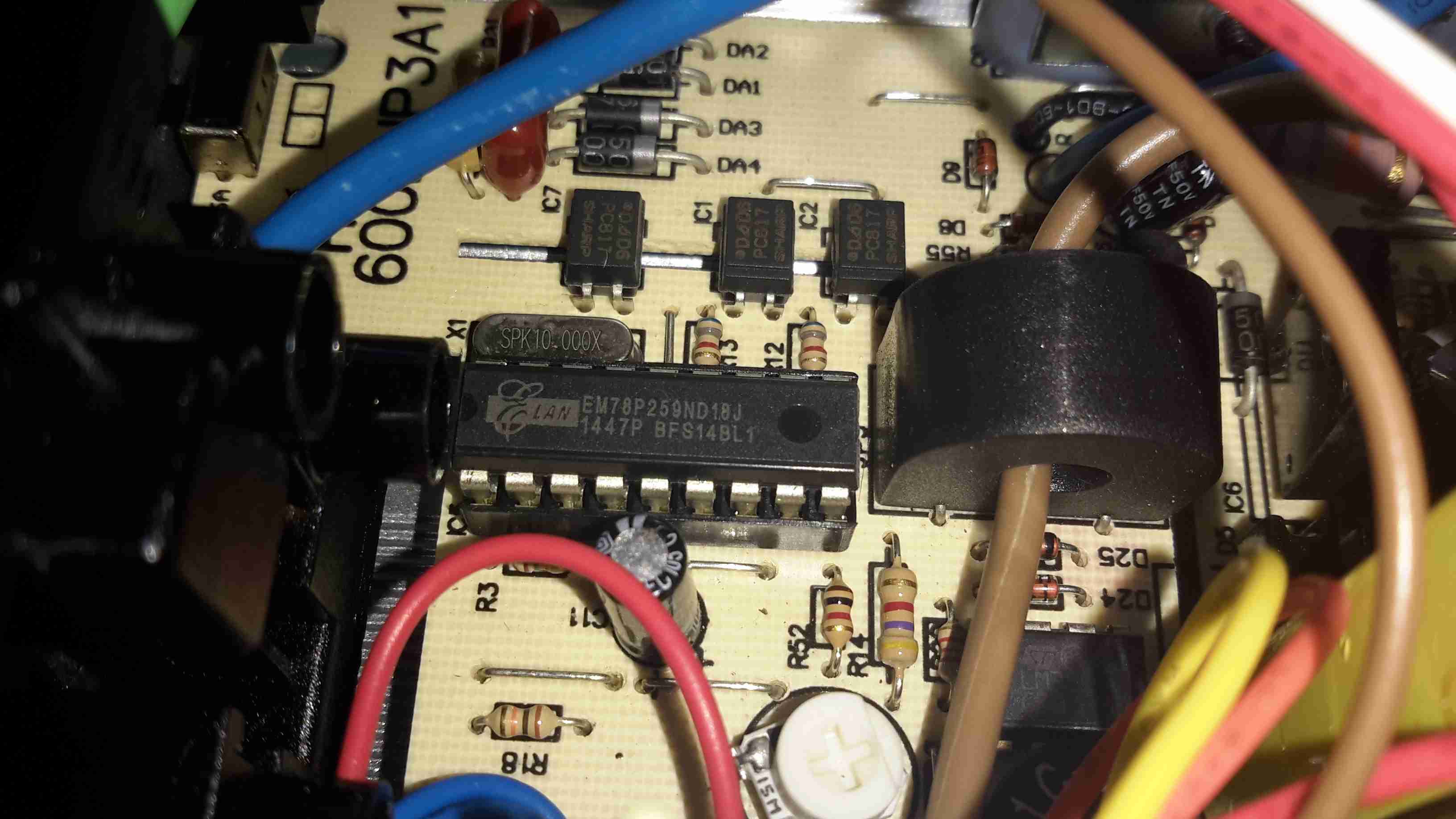
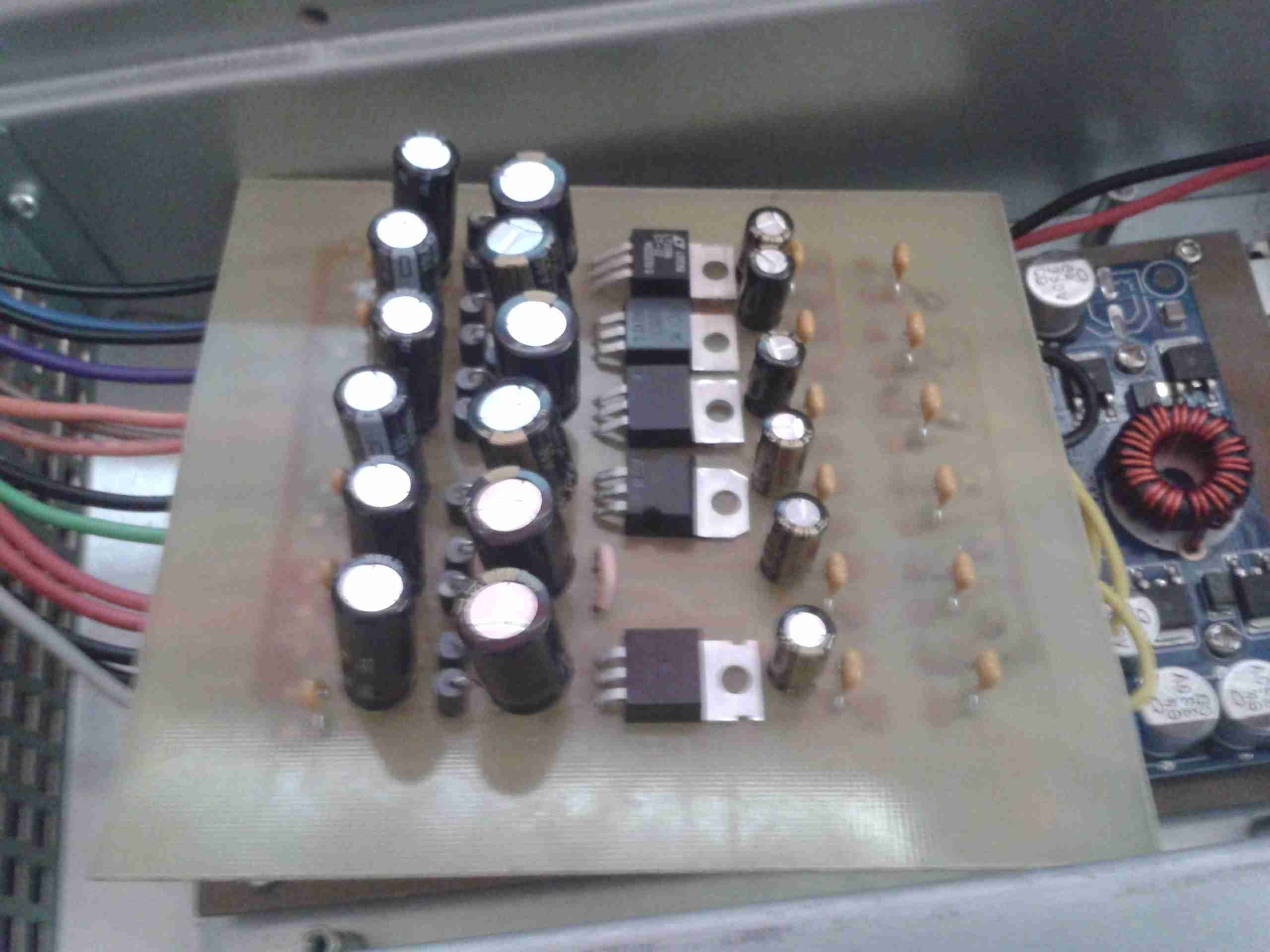
Driving the Solenoids
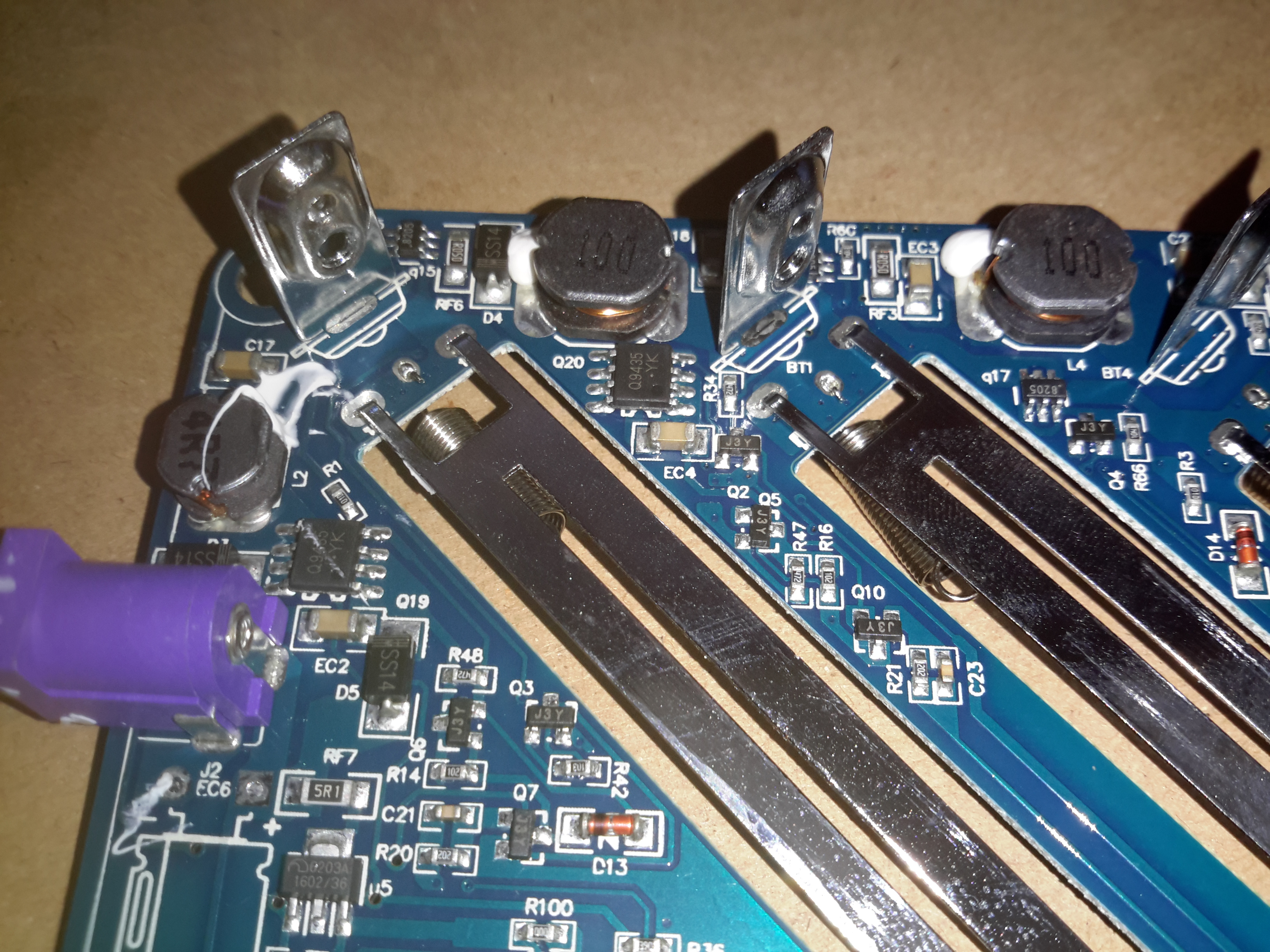
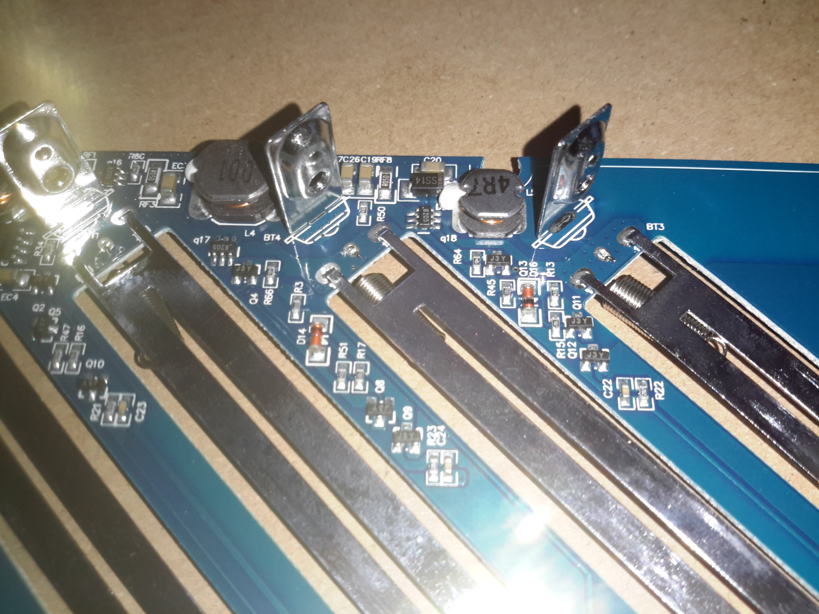
A closer view of the board shows the trip of dual H-Bridge drivers on the board, which will soon be hidden underneath the attenuator block. These are LB1836M parts from ON Semiconductor. Each chip drives a pair of solenoids.
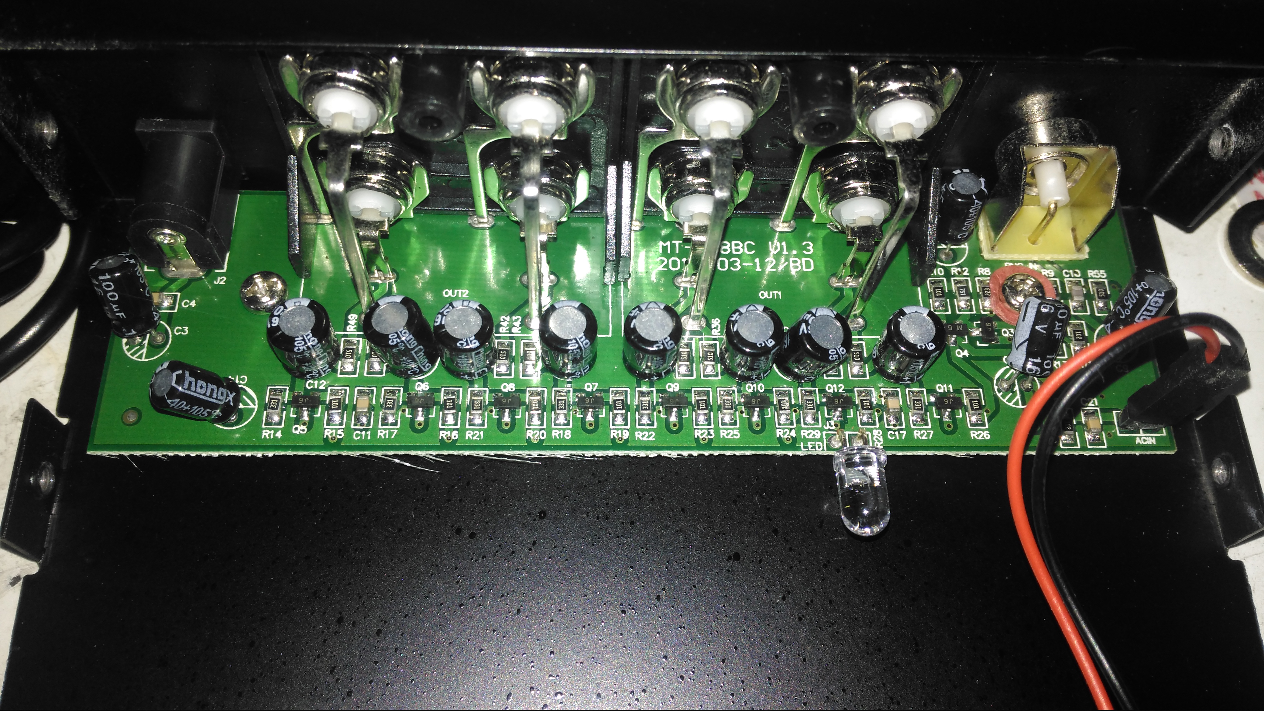
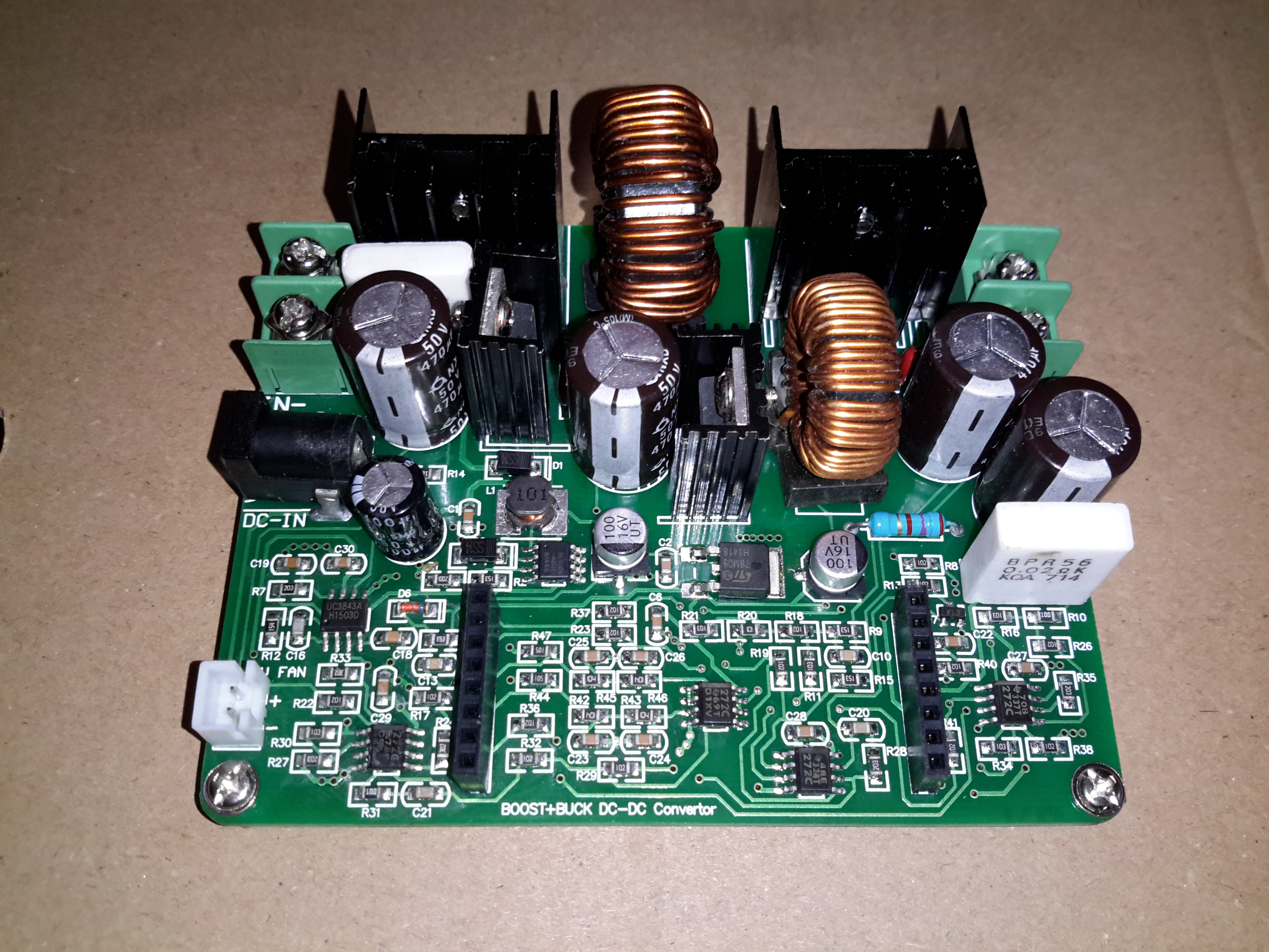
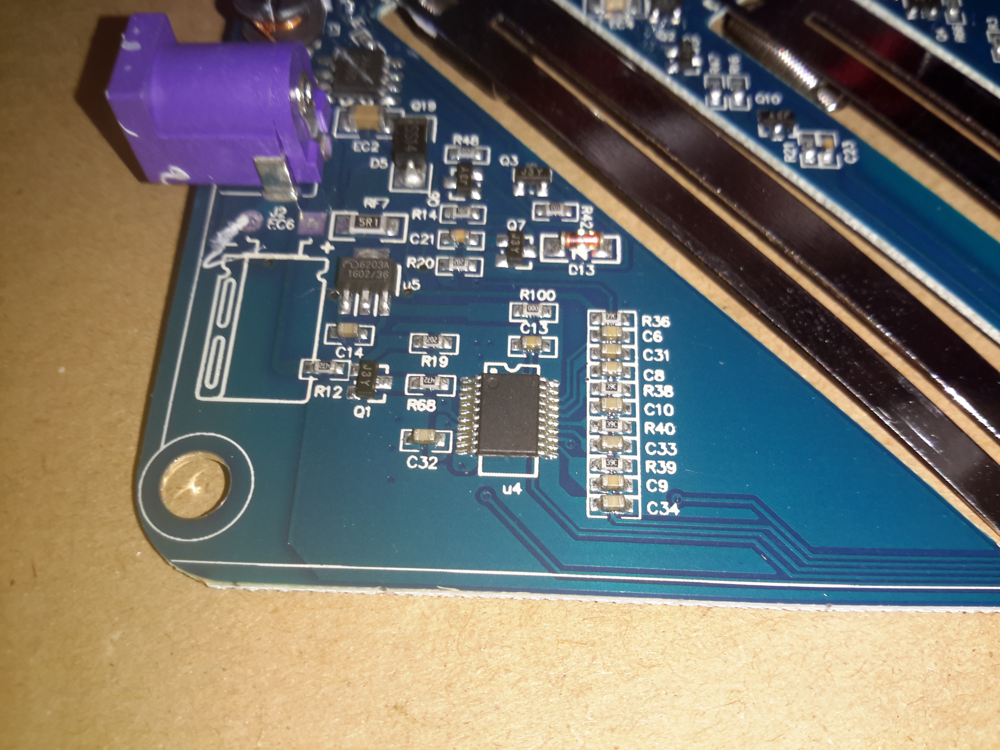
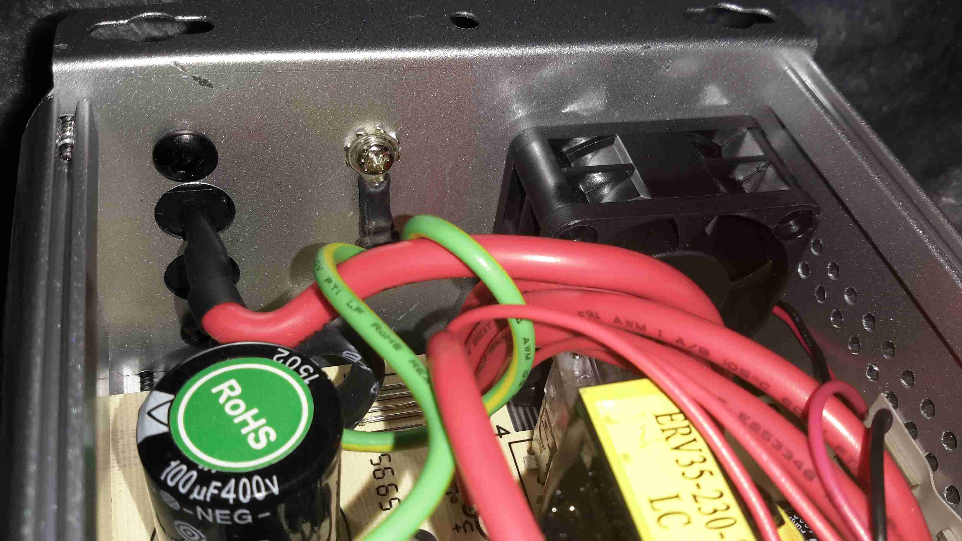
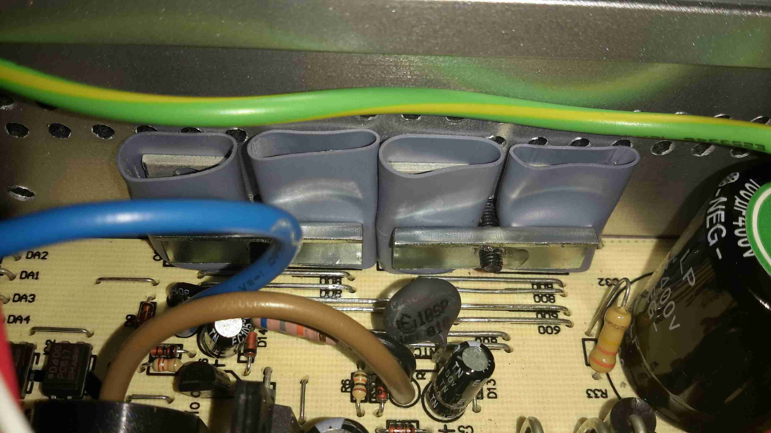
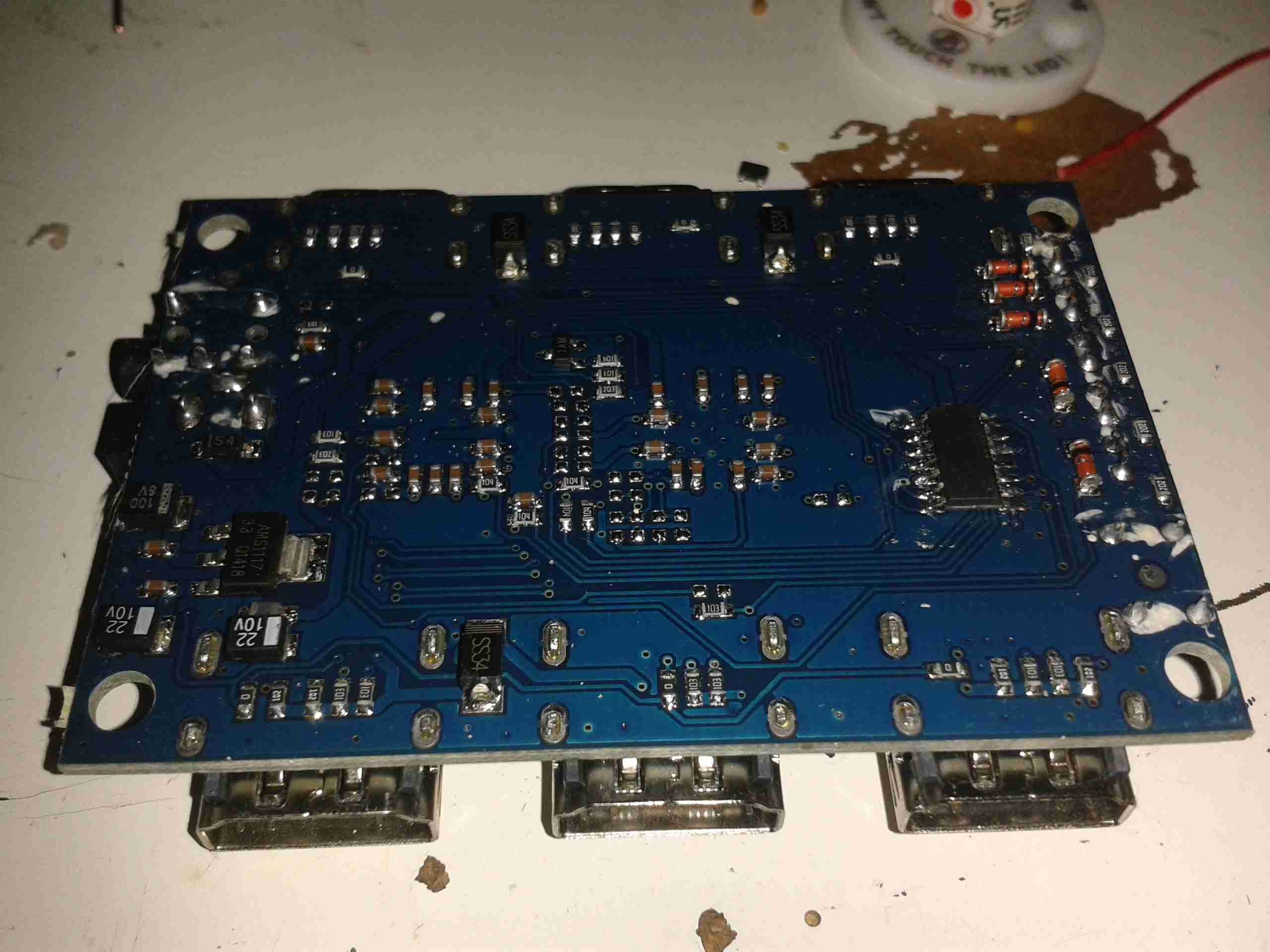
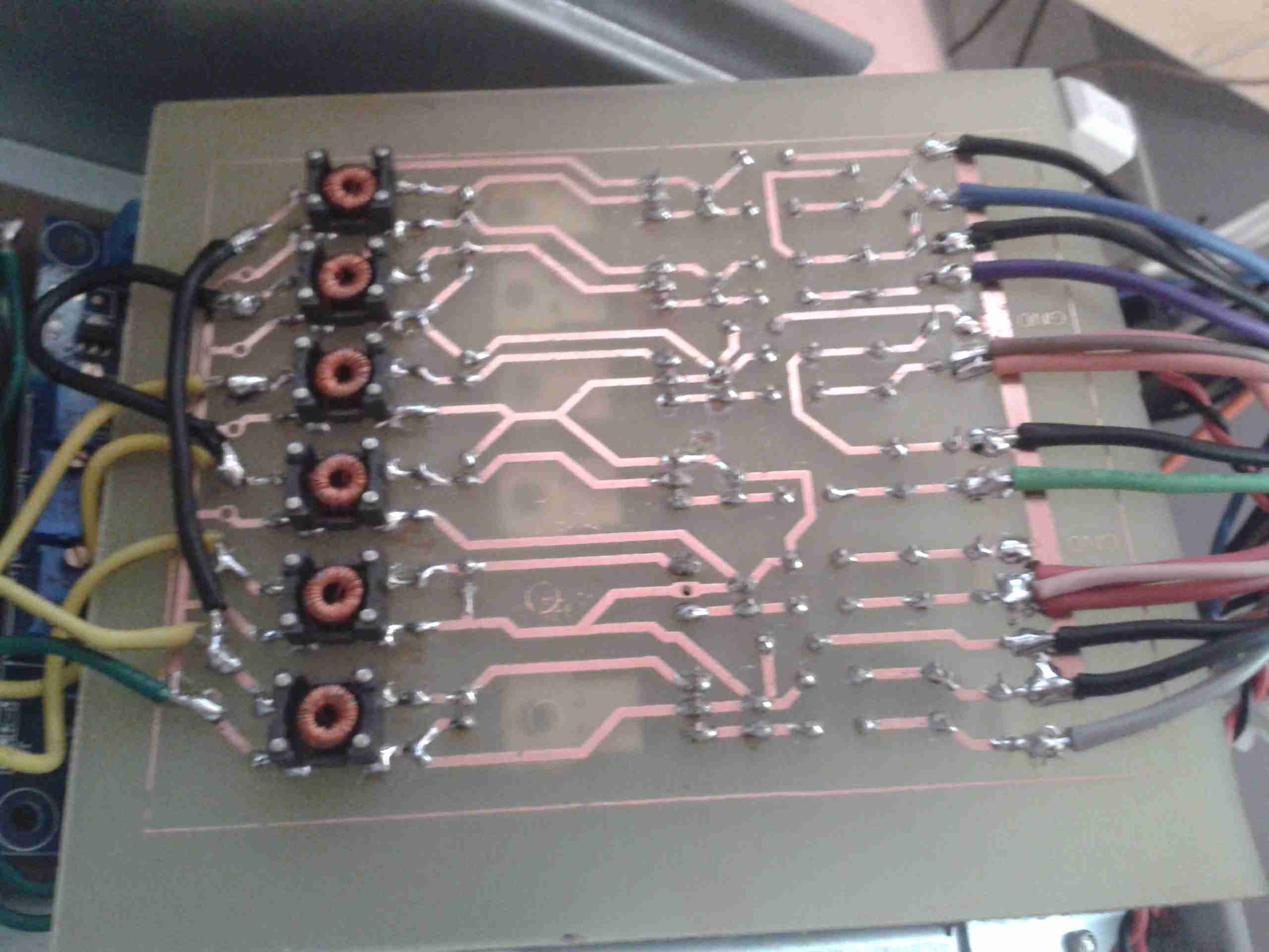
Power Supplies
The bottom of the board has all the power control circuitry, which are modularised for ease of production. There’s a Lithium charge & protection module for the 18650 onboard cell, along with a boost converter to give the ~9v rail required to operate the attenuator solenoids. While they would switch at 5v, the results were not reliable.
Finishing off
A bit more time later, some suitable firmware has been written for the Arduino, and the attenuator block is fitted onto the PCB. The onboard OLED nicely shows the current attenuation level, battery level & which input is selected.
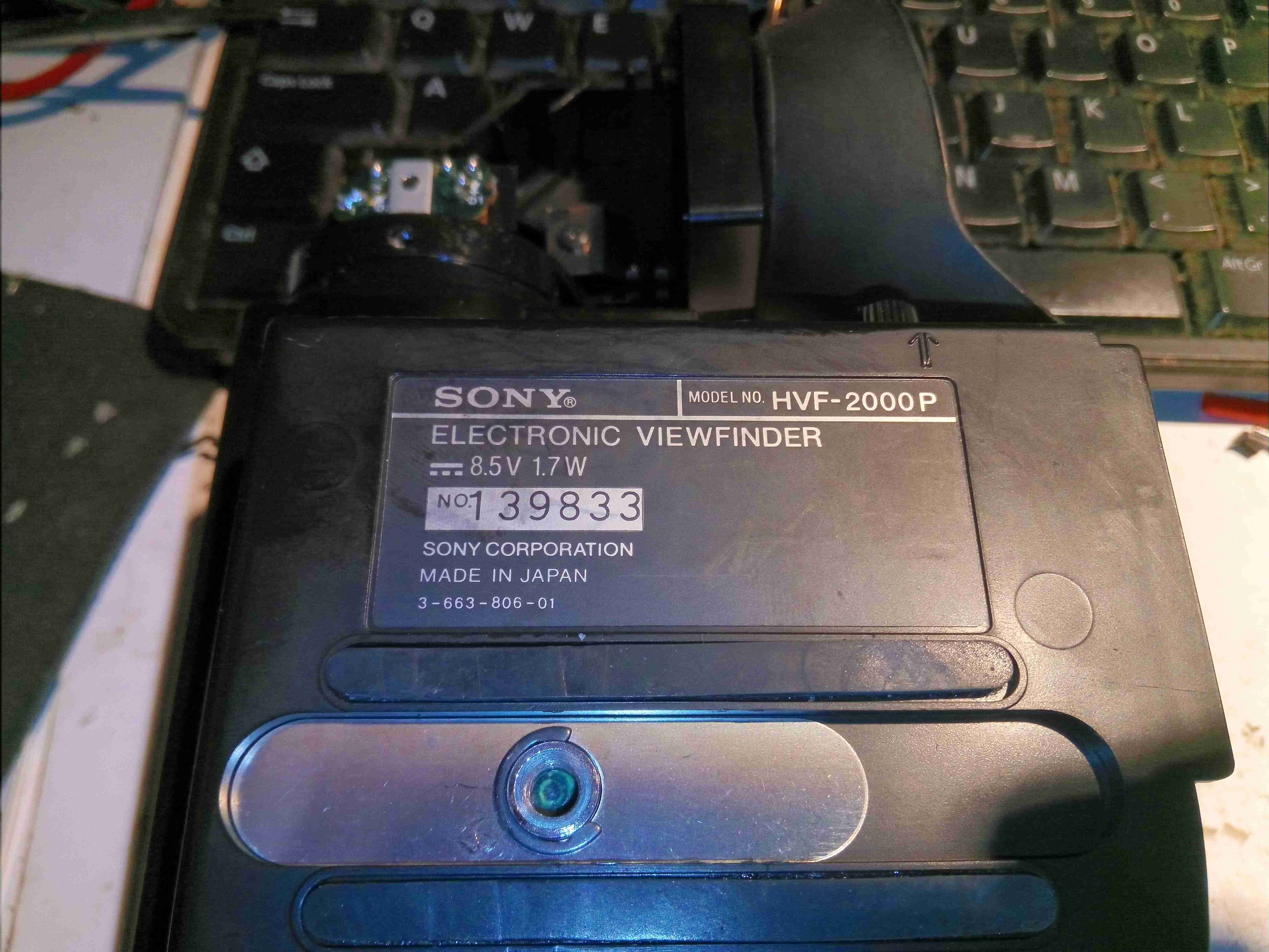
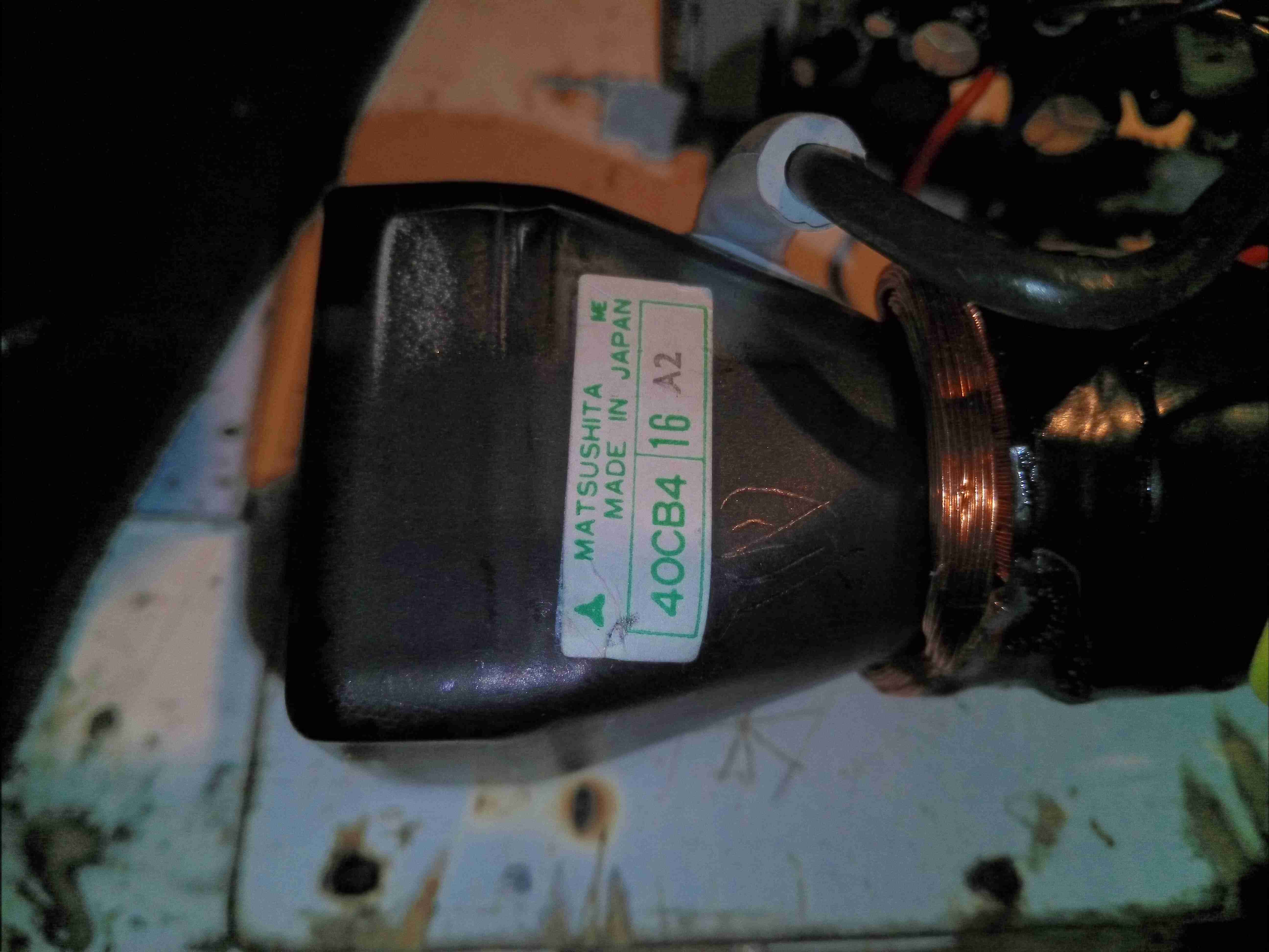
Well, it’s time for another viewfinder hack! I’ve been after one of these for a while, this is from an early 1980’s era Sony Trinicon camera, and instead of the tiny ½” round CRT display, these have a 1.5″ square CRT – a Matsushita 40CB4. Luckily I managed to score a pair of these from eBay for very little money. Update: The second camera’s viewfinder module turned out to have a dead flyback transformer, but at least I have a good spare CRT & the rest of the support components. More to come later on the teardown of the camera itself.
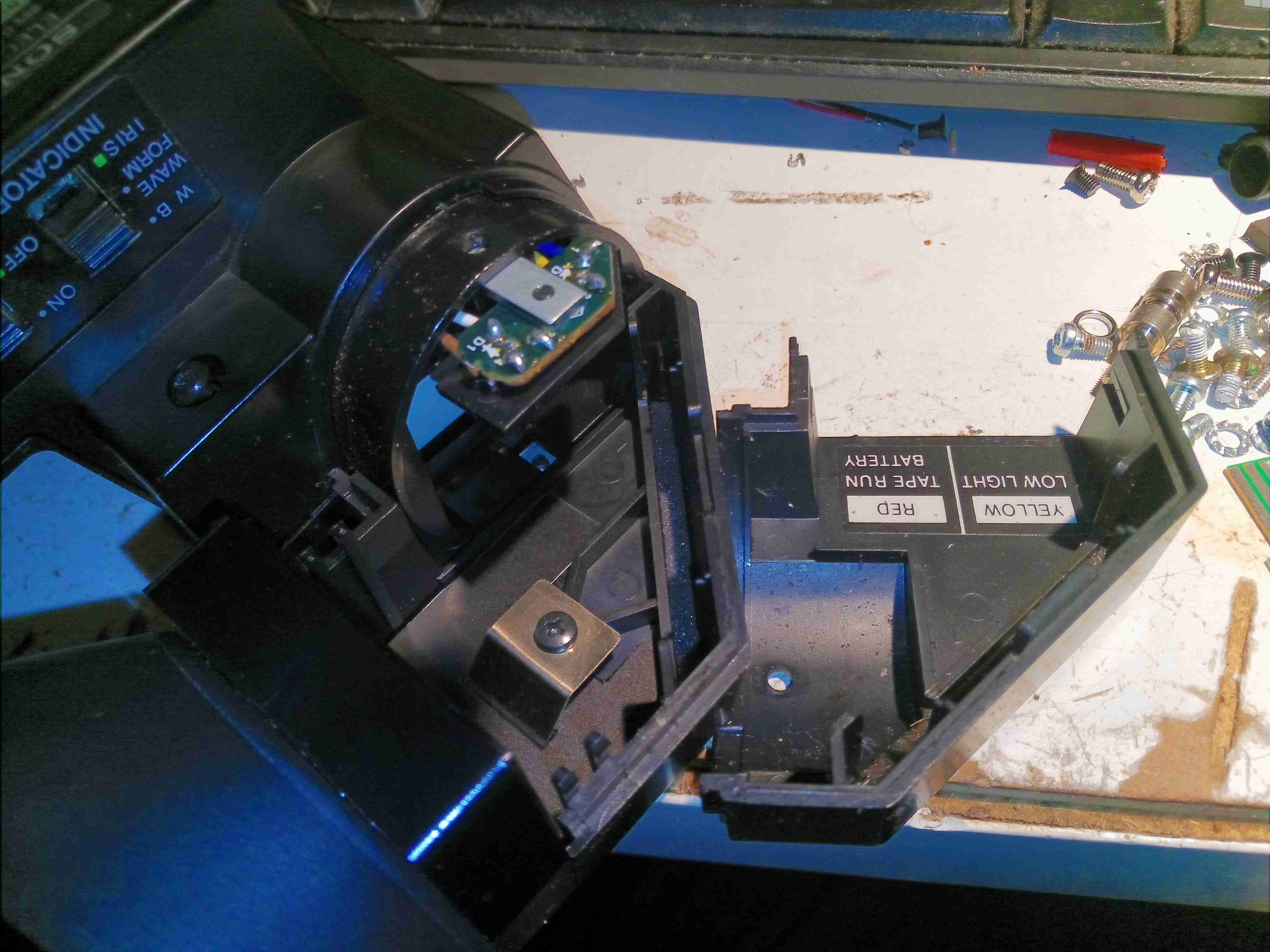
Mirror & Eyecup Assembly
The eyecup assembly with the magnifying lens & turning mirror is easy to remove, with clips & a single screw holding it onto the CRT holder sticking out of the side of the main casing.
Top Cover Removed
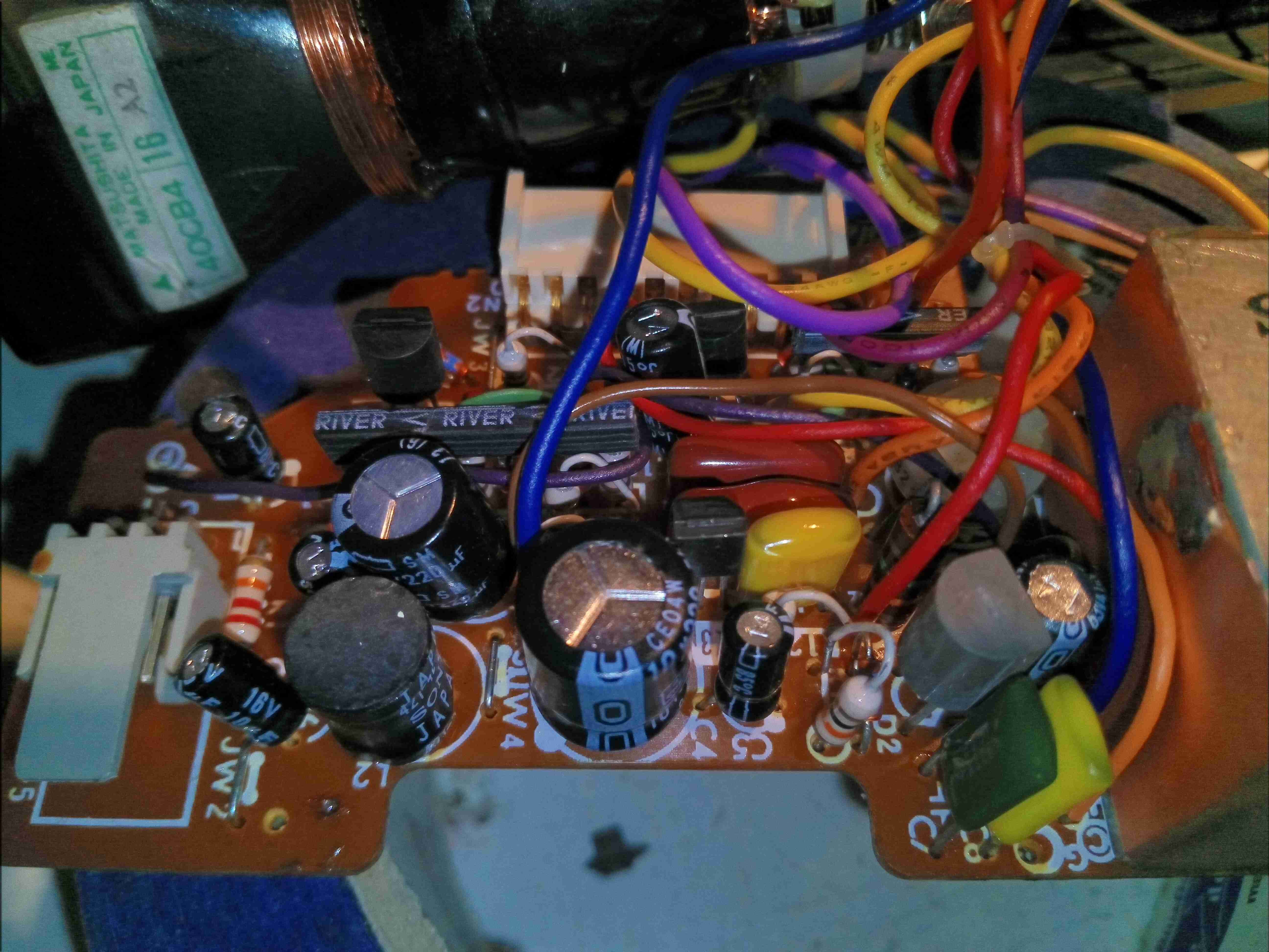
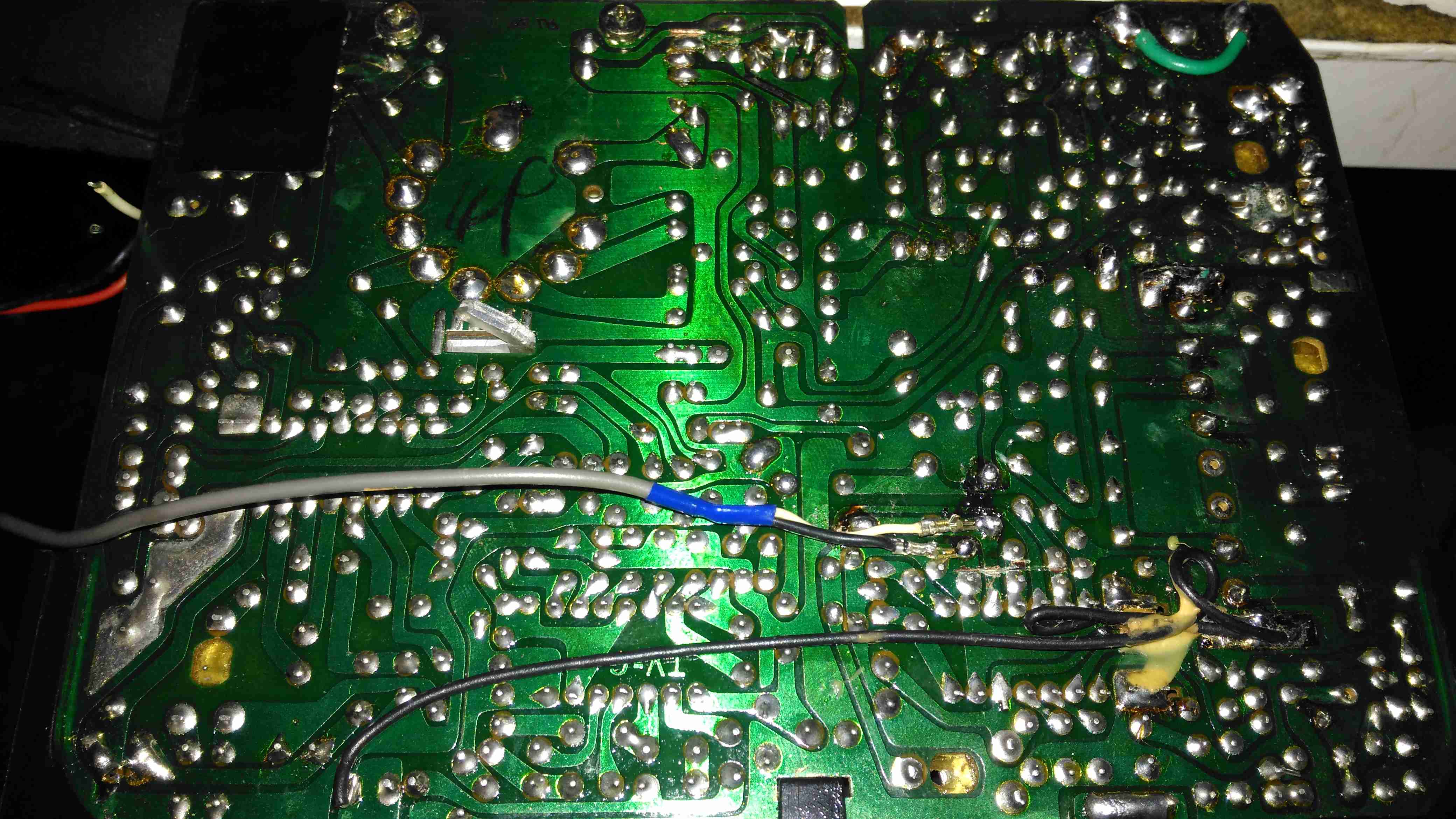
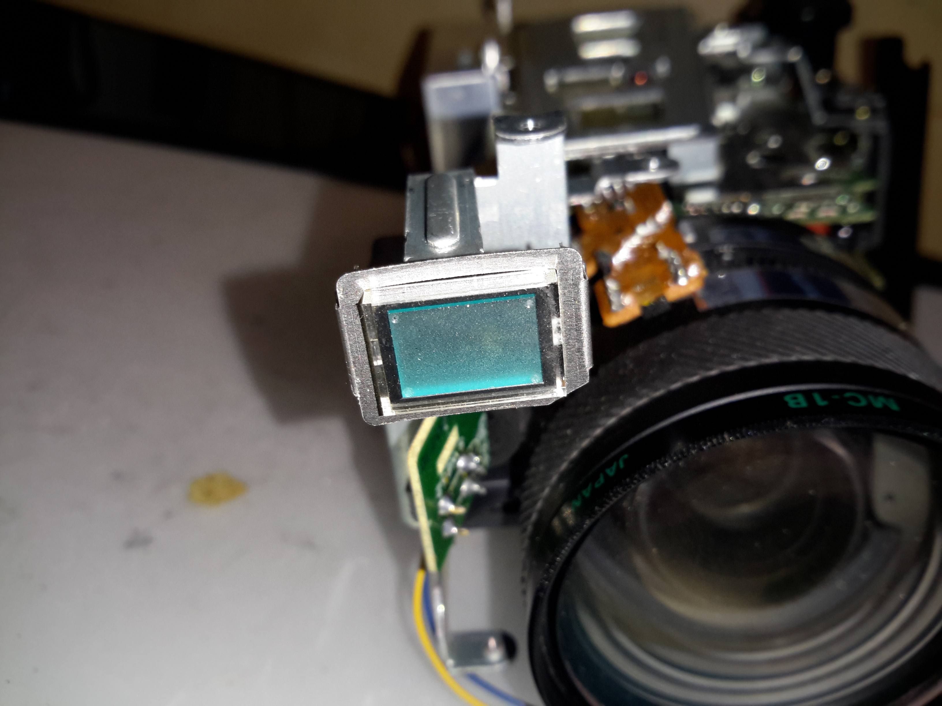
Removing some screws around the case allows the top cover to be removed, revealing the electronics. There’s certainly more in here than the later camera viewfinders, in this unit there are two boards slotted together with a board-to-board interconnect at the bottom. The CRT is at the top of the photo, hiding inside the plastic housing & deflection yoke assembly.
Bare PCBs & CRT
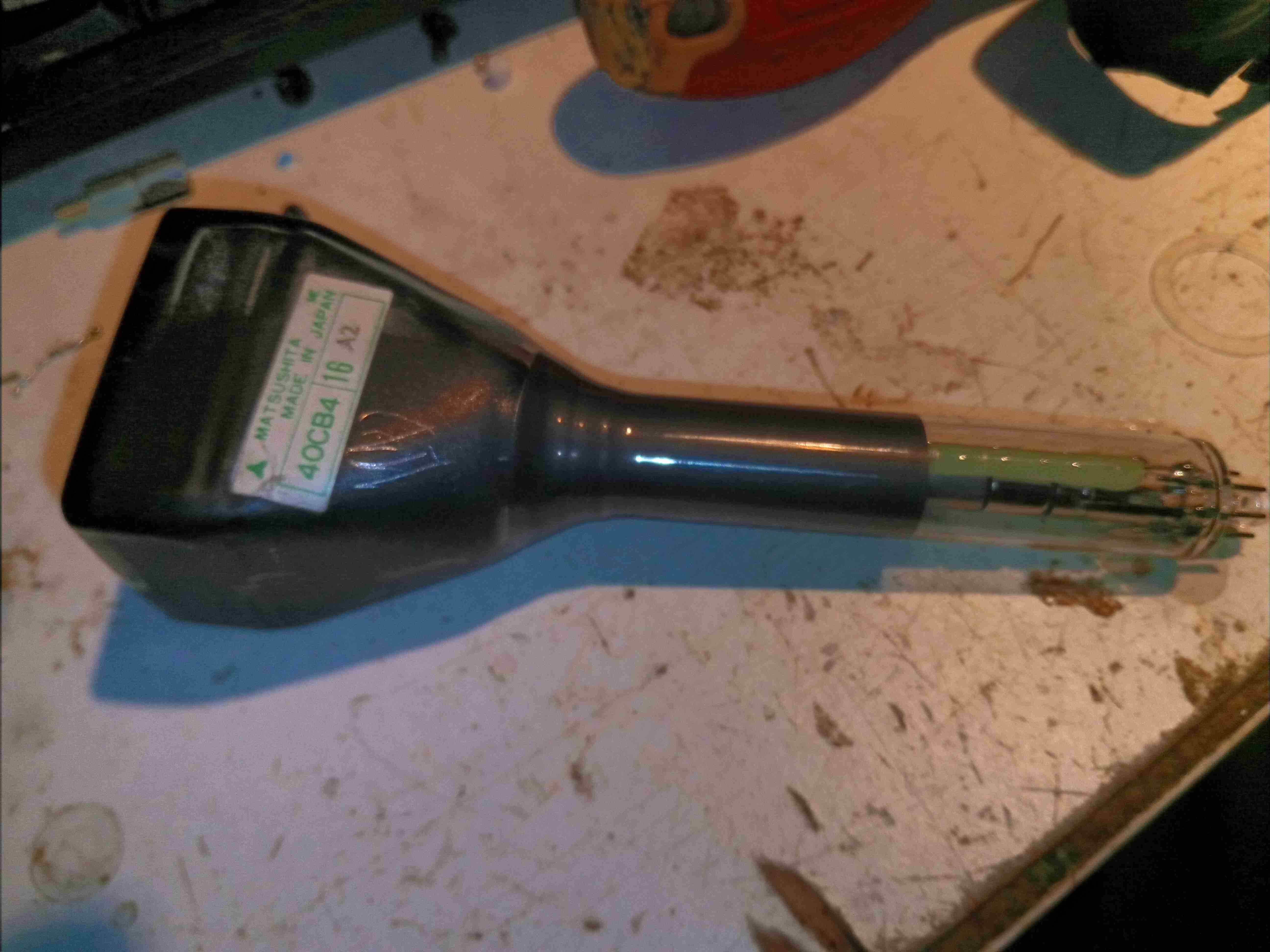
Here’s the CRT & one of the control boards removed from the case, having been stripped of the heatshrink tube that held the final anode lead in place. Just like on larger CRTs, this viewfinder has the final anode on a cavity connector fused into the bell, instead of being led out to a pin on the base. This is probably due to the much higher anode voltage of 5kV, a big jump from the 2kV on the ½” round tubes.
40CB4 CRT Label
Yup, it’s definitely the elusive 40CB4. Apparently these CRTs are still manufactured to this day for professional camera viewfinders, as the resolution of this small vacuum tube is still better than similarly sized modern tech such as LCDs or OLEDs. The phosphor used is type P4 – ZnS:Ag+(Zn,Cd)S:Ag, with an aluminized overcoat.
Bare 40CB4 CRT
After the base connector & deflection yoke are removed from the tube, the very long neck can be seen, this long glass neck apparently giving better focus & resolution than the stubbier tubes.
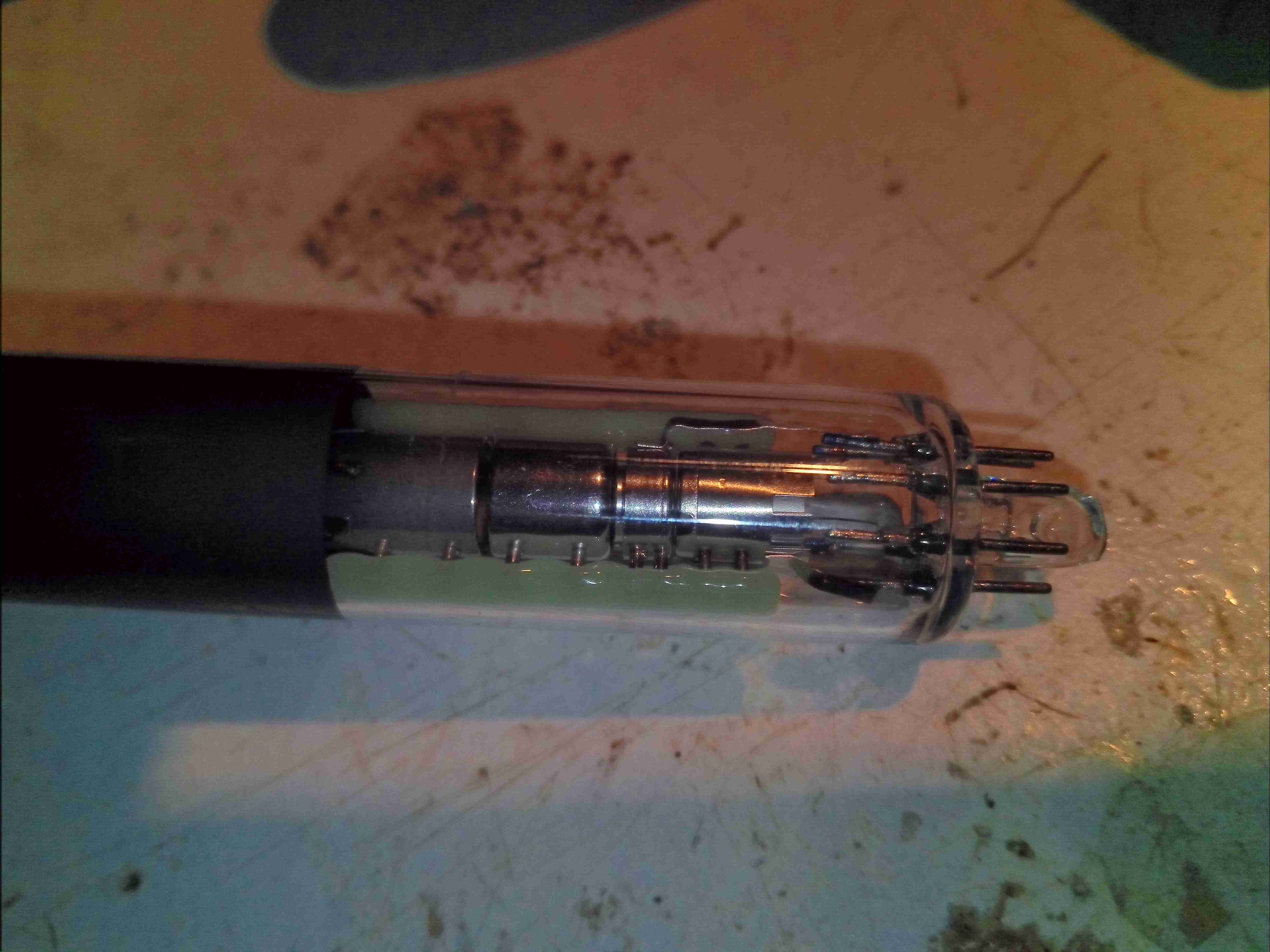
Electron Gun
The electron gun is the usual single unit as usually found in monochrome tubes.
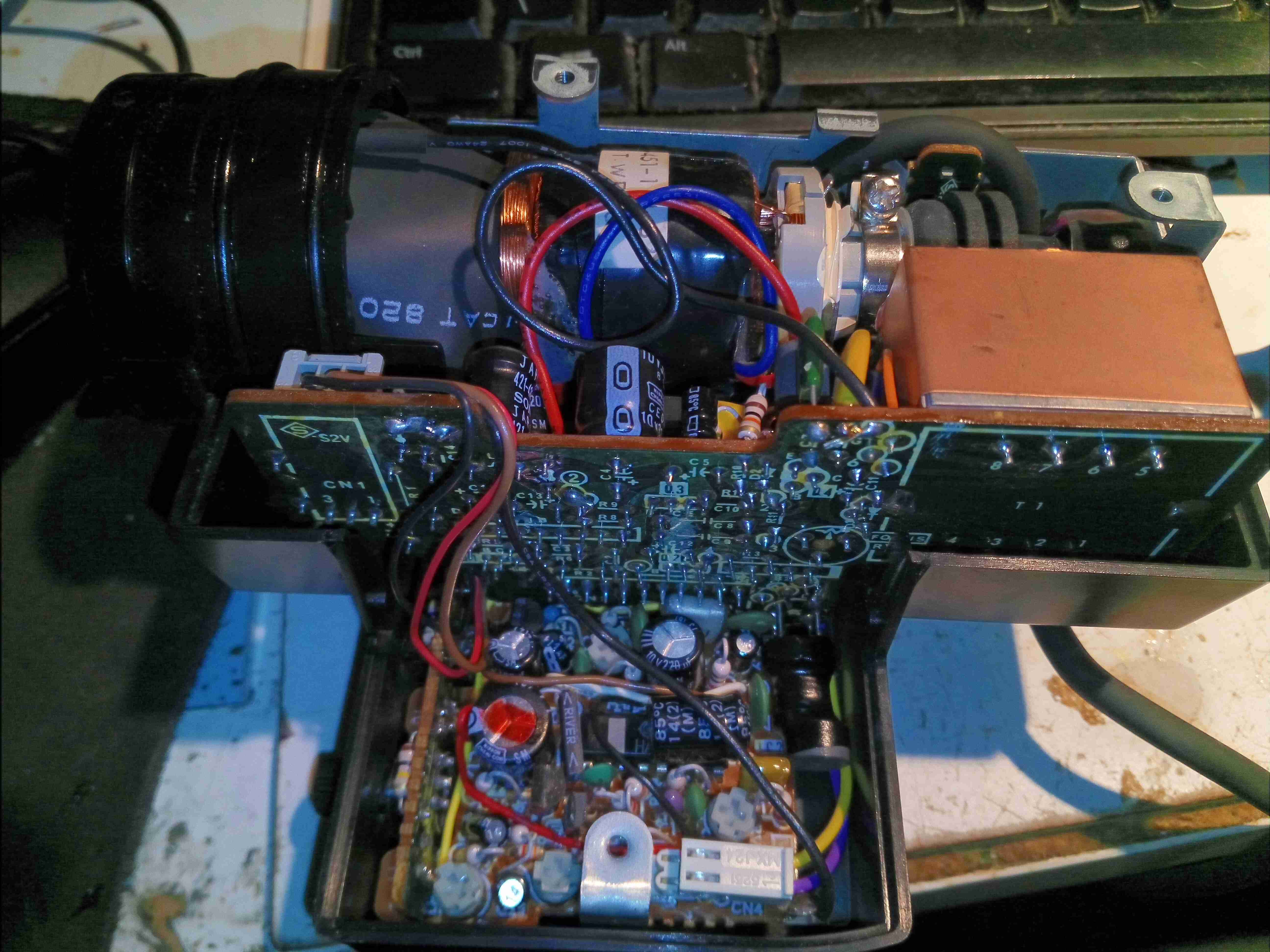
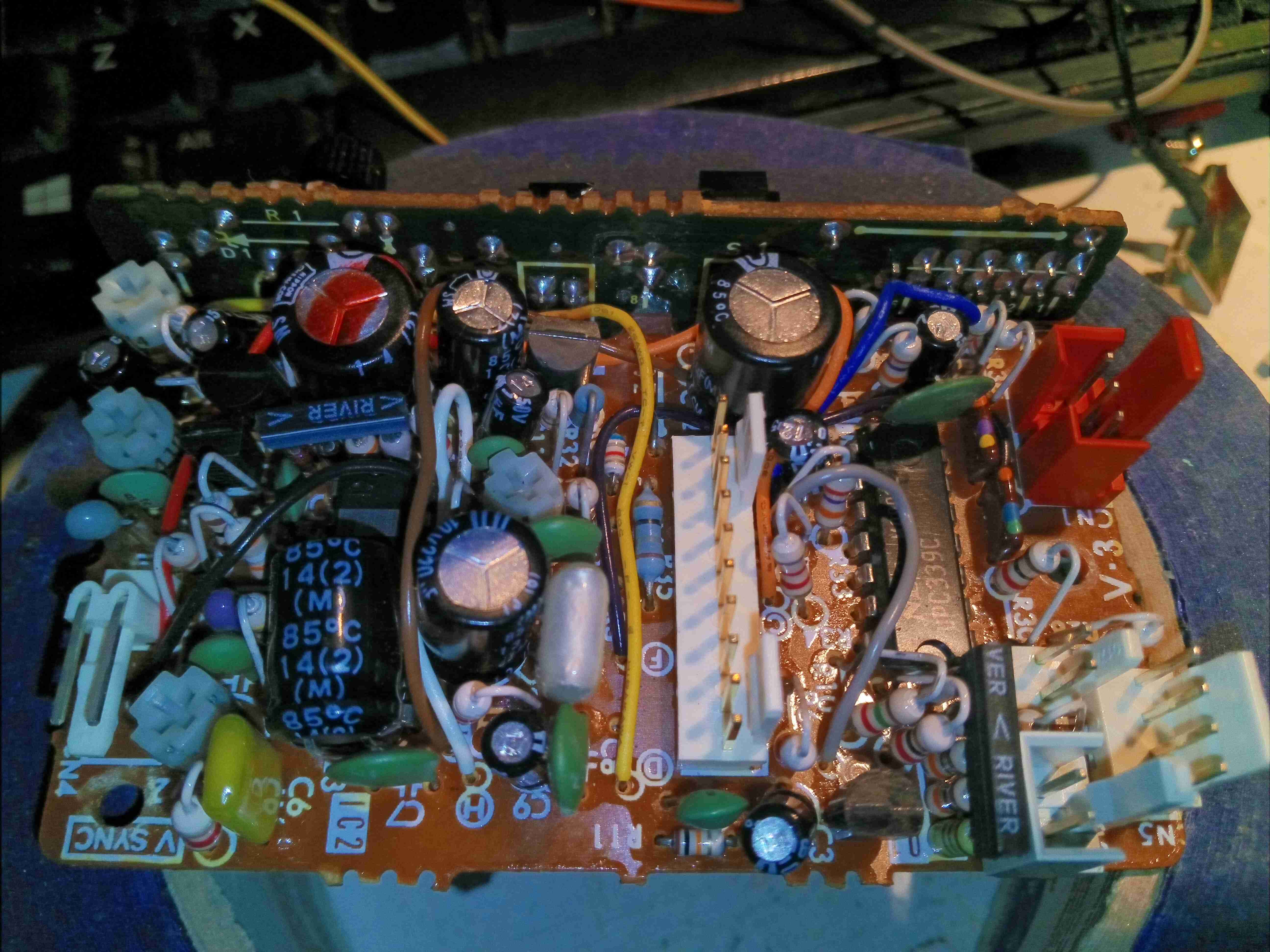
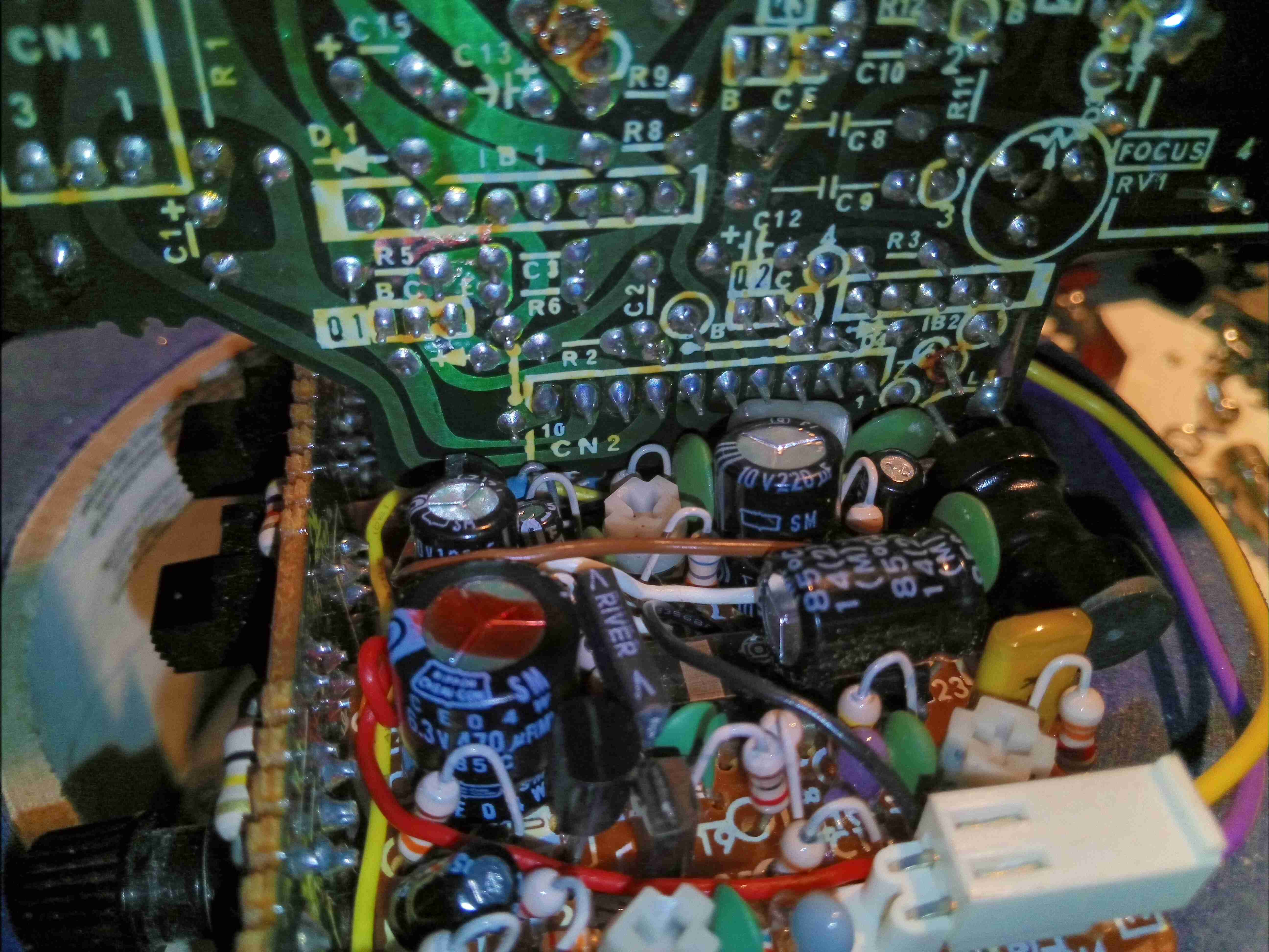
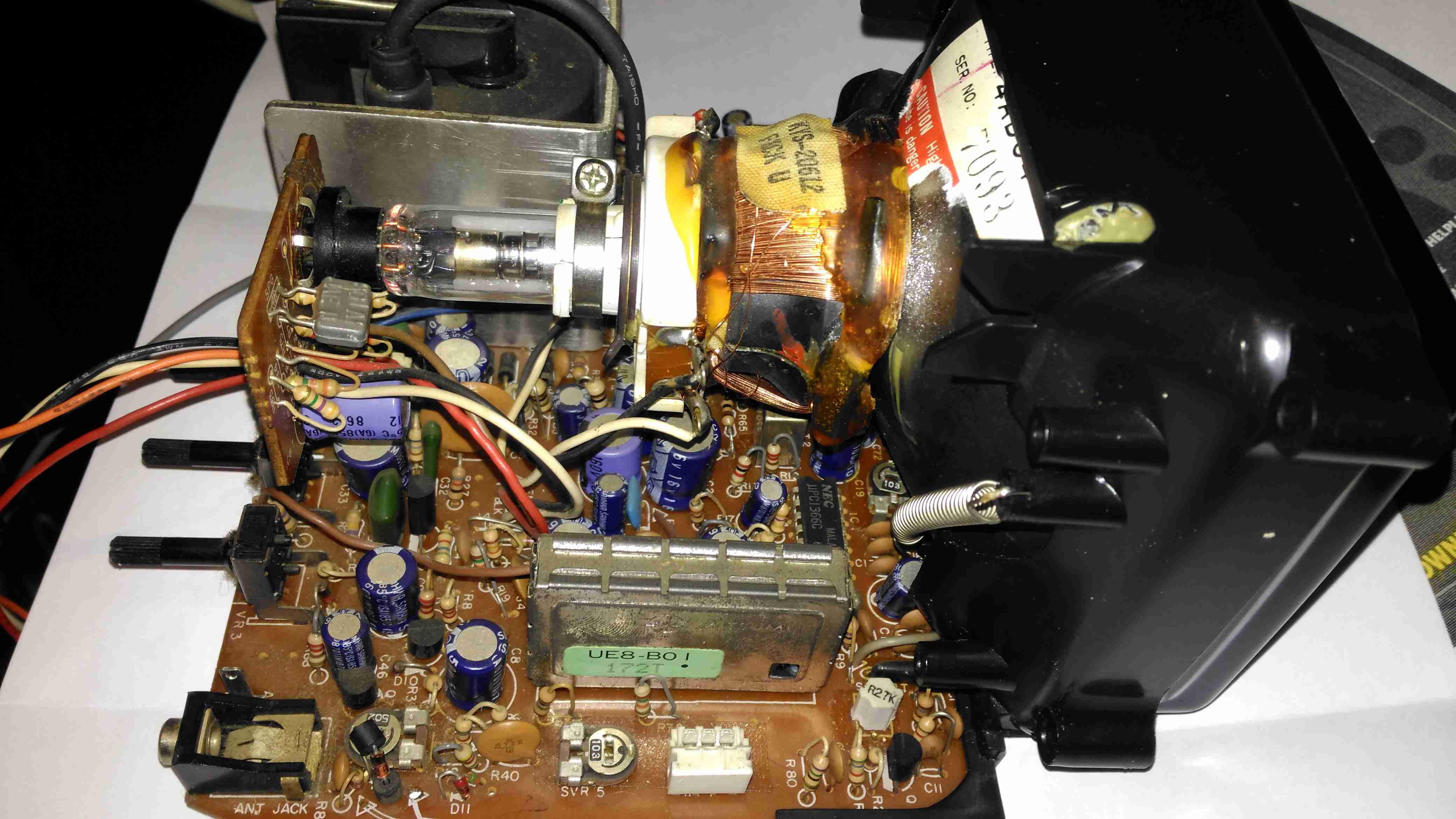
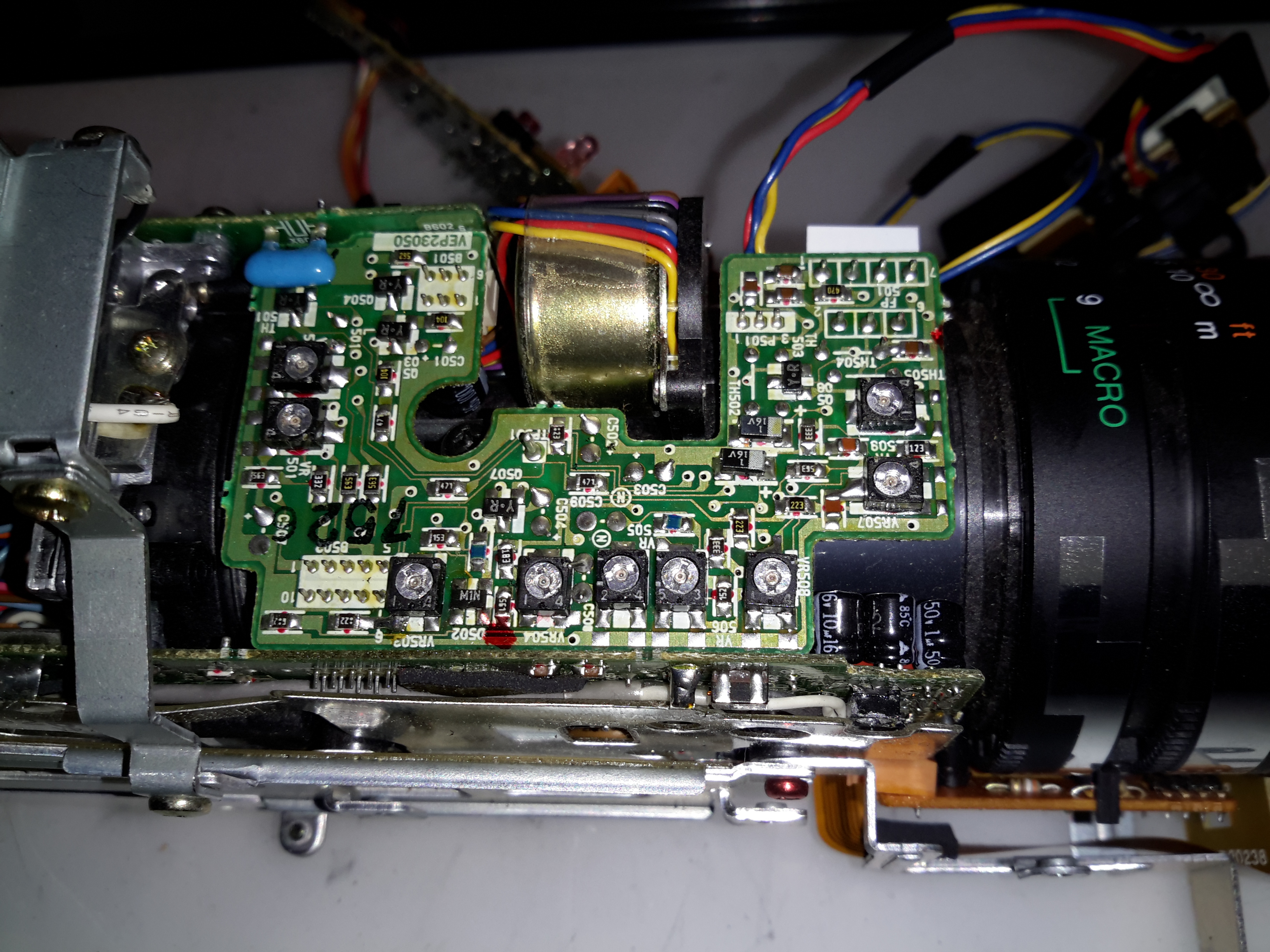
Deflection Board
The bottom board in the assembly has all the control circuitry for the CRT, including the HA11244 deflection IC, composite sync separator & vertical deflection drive circuit. There are also circuits here to display a video waveform on the CRT, along with iris & white balance markers.
Horizontal Board
The other board has the horizontal drive circuitry, along with the video input amplifier. Despite the attempt to miniaturize the entire assembly, these are still well packed boards. Some of the resistors & diodes are bussed together in custom SIL hybrid modules to save PCB space. Like all the other CRT viewfinders, these units are meant for viewing via a mirror – the horizontal deflection coil connections need to be reversed to show a correct image without the mirror. The Red & Blue wires to the yoke need to be swapped here.
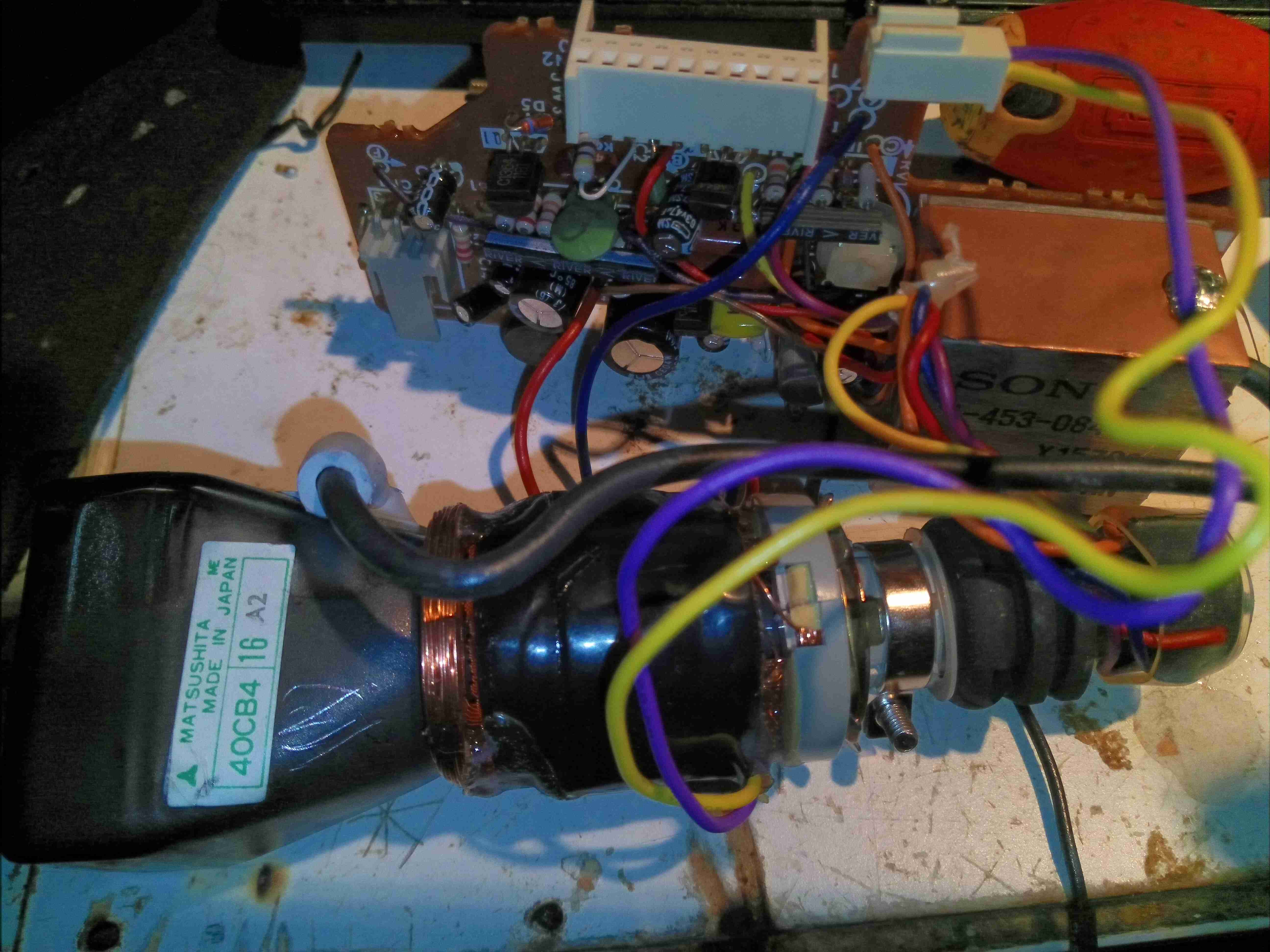
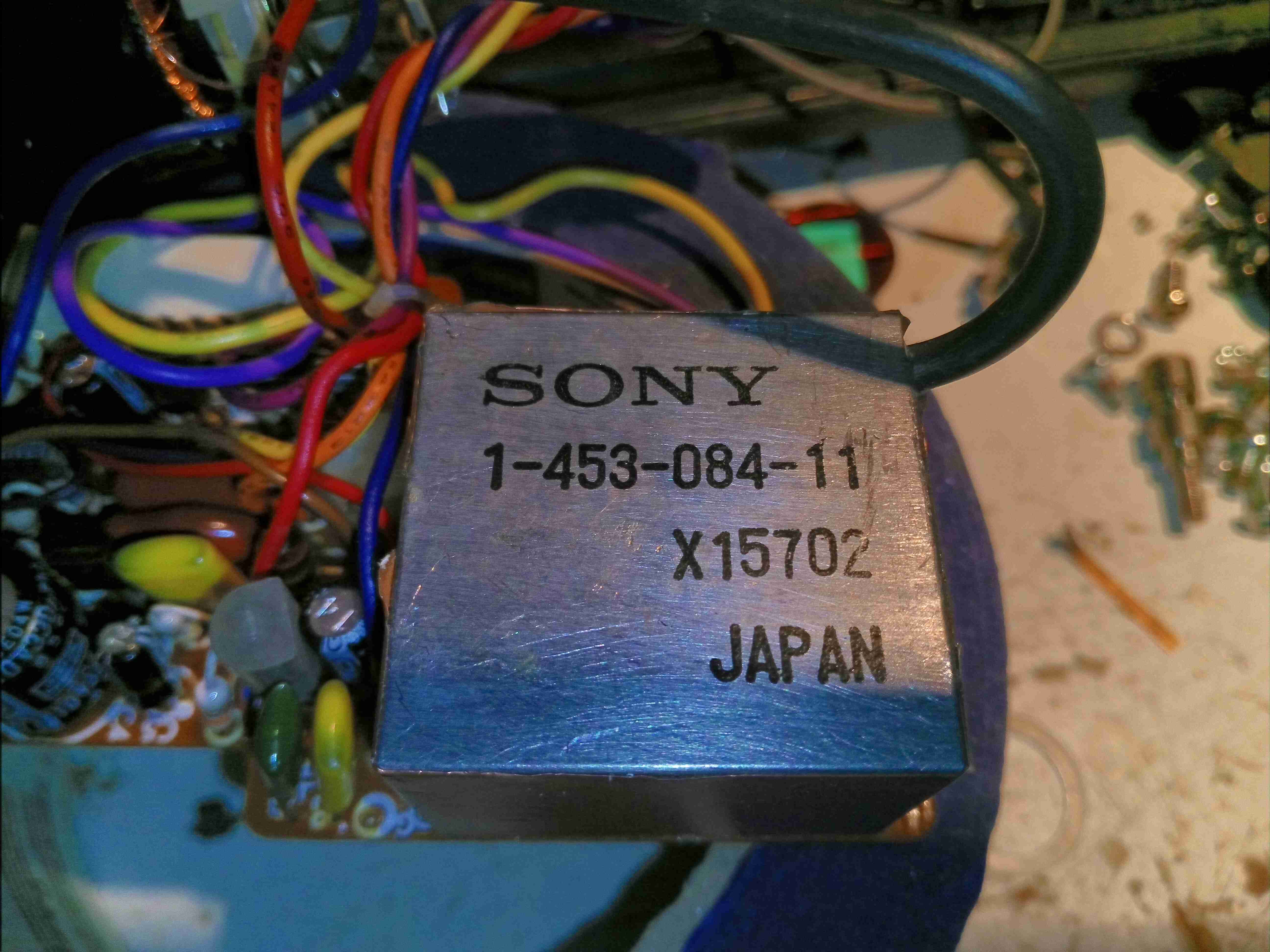
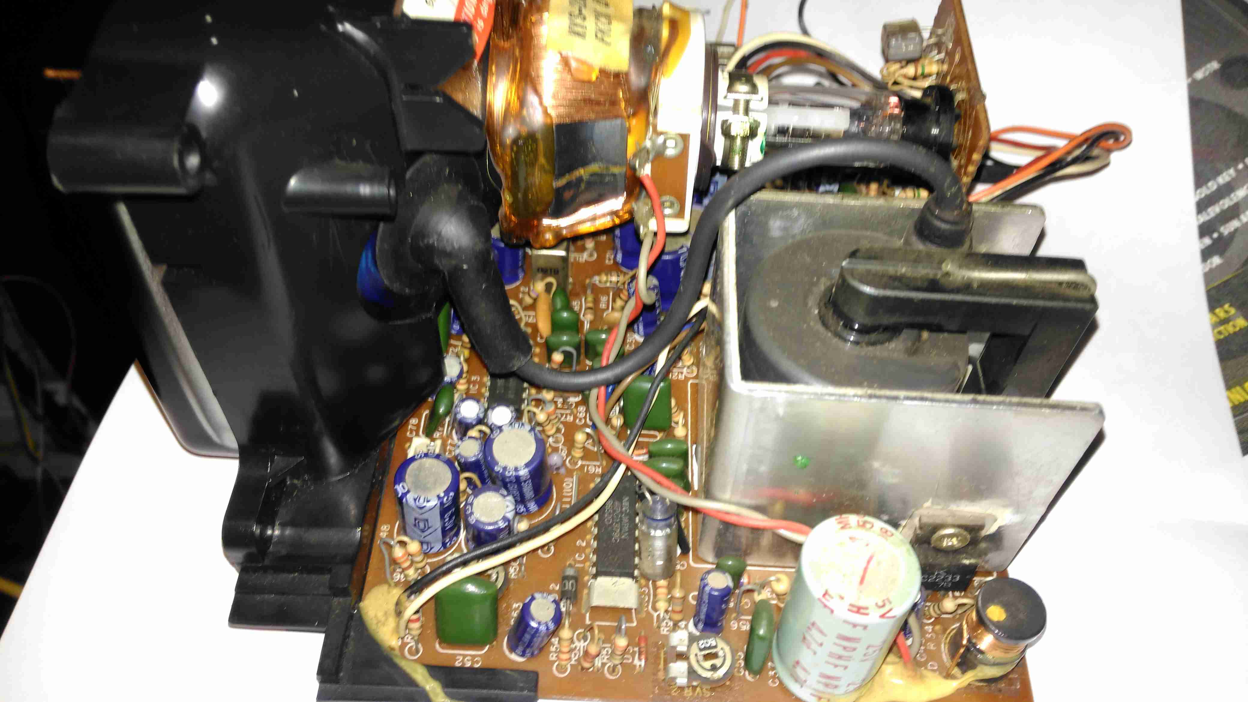
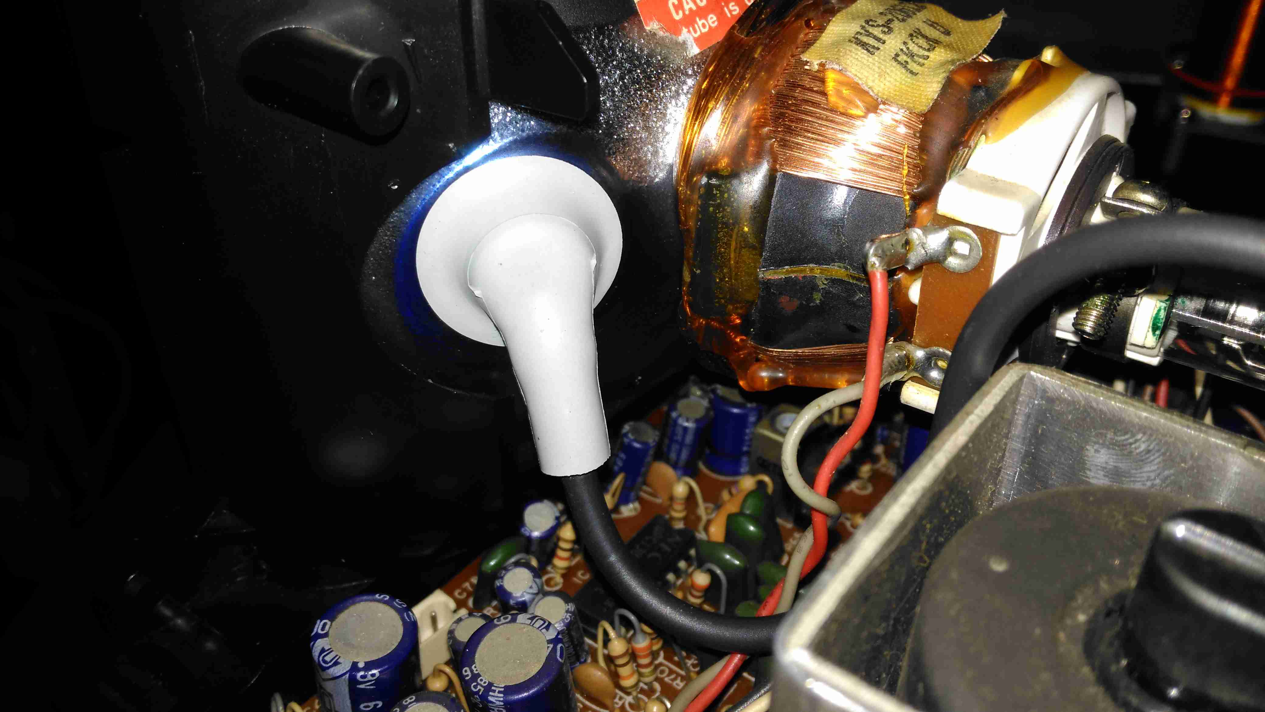
Flyback Transformer
The horizontal board on this unit also supports the flyback transformer, which is massive compared to the other viewfinder circuits. Biasing, focus & filament supplies for the CRT are also derived from this transformer, via auxiliary windings.
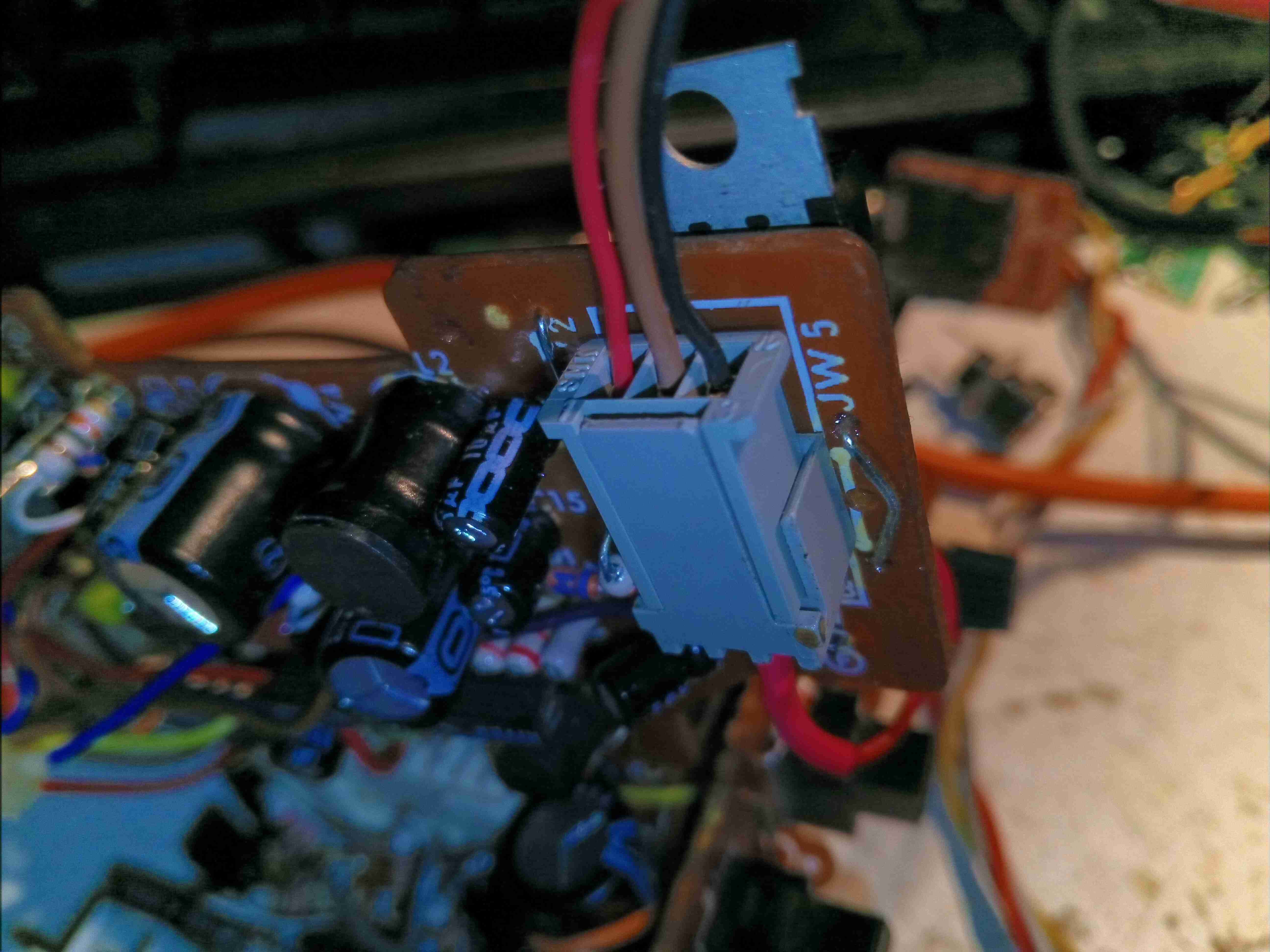
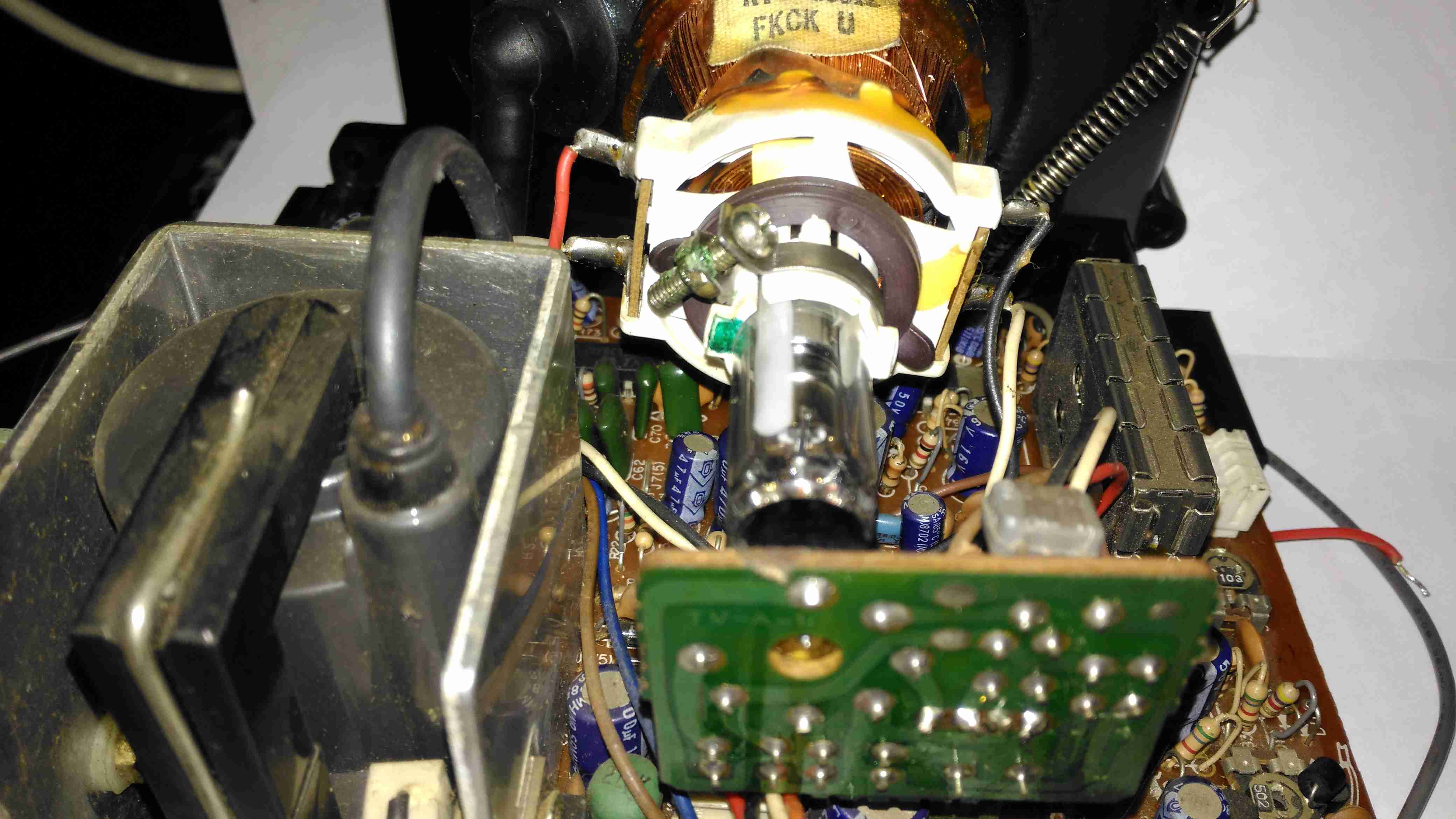
Boards Connected
The boards slot together in the centre to form the fully operational circuit.
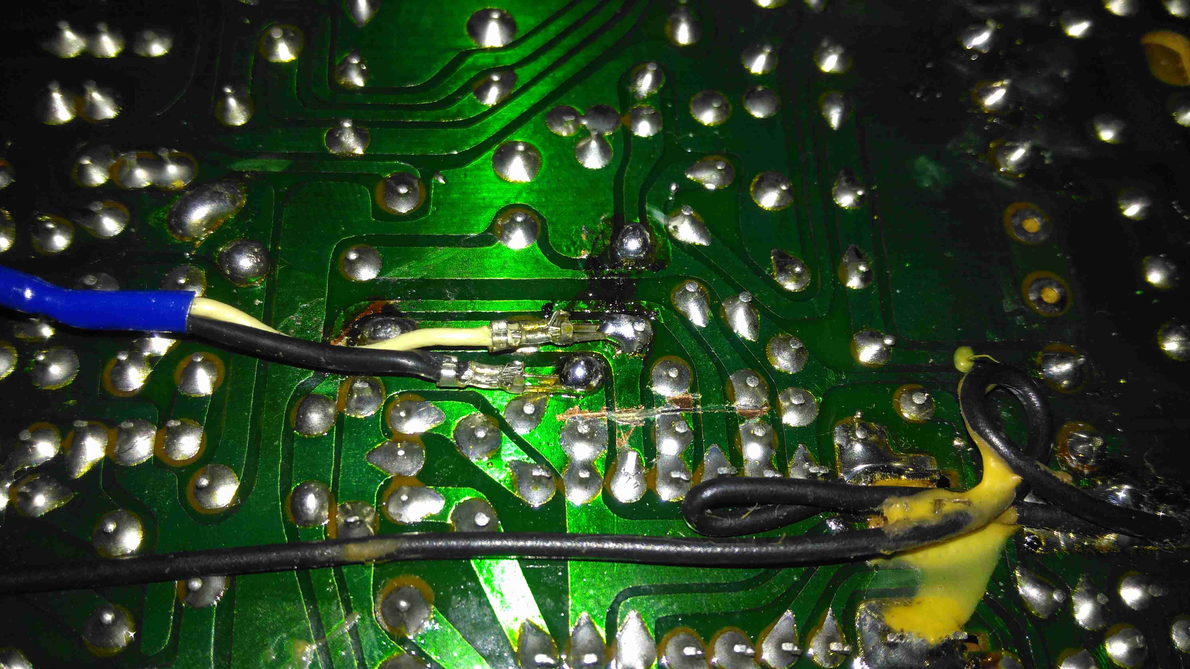
Video Input
Out of the 3 plugs emerging from the cable feeding the viiewfinder, only this one is important, on the horizontal drive board. Black is ground, Brown +8.5v & red is composite video input. There’s also a resistor tied into the positive rail to the video input pin, which pulls it high to 8.5v – this is R1 right next to this connector. Desolder this 22K resistor to help protect anything feeding a signal into the unit, like a RPi, it’s not needed for normal operation.
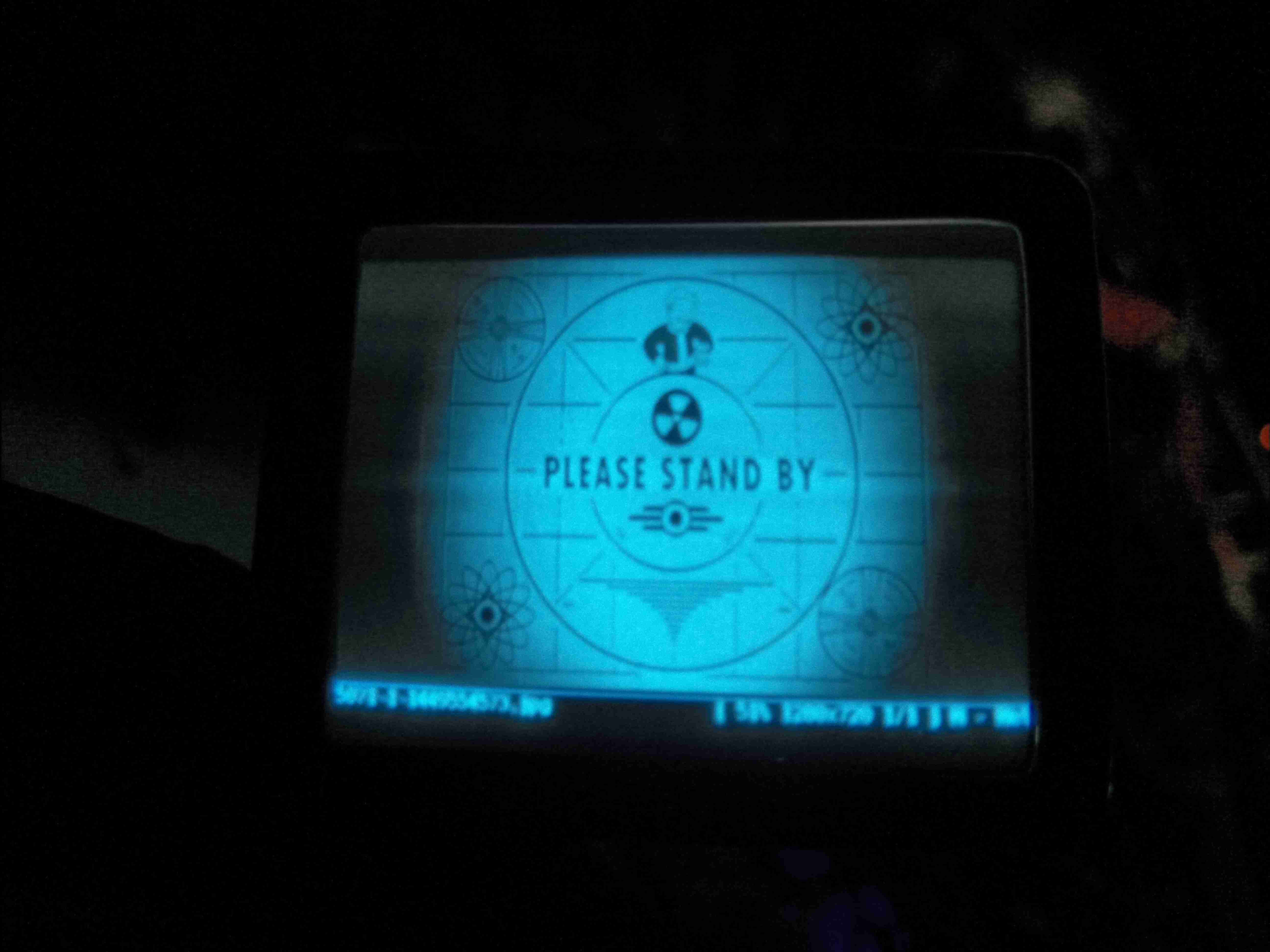
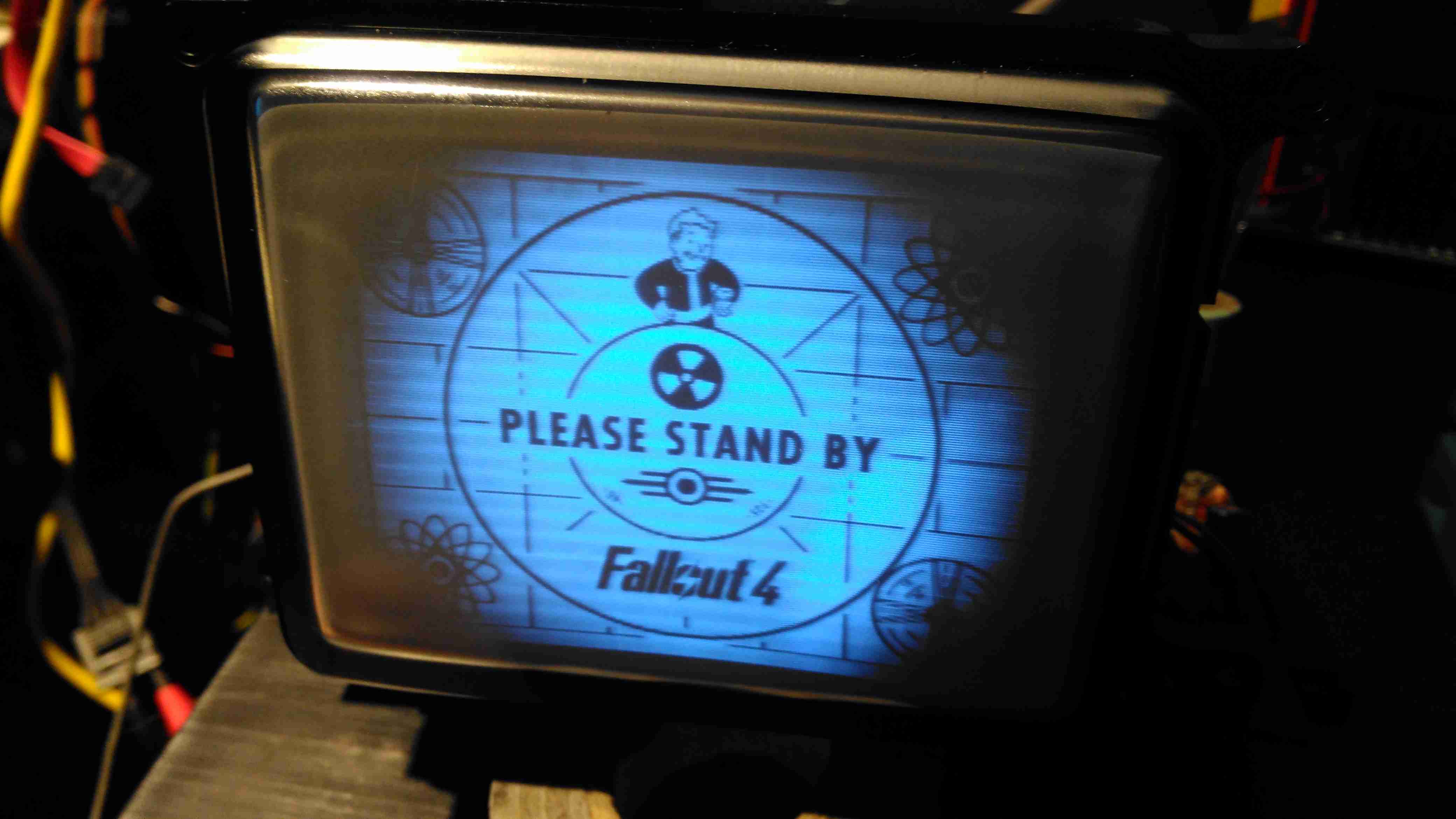
Fallout!
As usual for a CRT post, the Fallout loading screen on the display. The picture quality isn’t as good as it should be, probably due to the noisy buck-converter I have rigged up for testing. If it doesn’t get better with a linear regulator, I’ll start replacing the 39 year old electrolytic capacitors. Current draw is 130mA at 7.5v. Schematics for this unit & the CRT datasheet are available below:
Here’s the CRT & it’s drive board removed from the main chassis. Nicely modular this unit, all the individual modules (radio, tape, TV), are separate. This is effectively a TV itself, all the tuner & IF section are onboard, unlike in other vintage units I’ve modified, where the tuner & IF has been on a separate board. There’s a 3-pin header bottom centre for the tuning potentiometer, and external antenna input jack. The internal coax for the built in antenna has been desoldered from the board here. here a the usual controls on the back for adjusting brightness, contrast & V Hold, all the other adjustments are trimmers on the PCB.
Unfortunately after 30+ years of storage, this didn’t work on first power up, neither of the oscillators for vertical or horizontal deflection would lock onto the incoming signal, but a couple of hours running seemed to improve things greatly. The numerous electrolytic capacitors in this unit were probably in need of some reforming after all this time, although out of all of them, only 21 are anything to do with the CRT itself.
Anode Cap
Here’s the anode side of the unit, with the small flyback transformer. The rubber anode cap has become very hard with age, so I’ll replace this with a decent silicone one from another dead TV. The Horizontal Output Transistor (a 2SC2233 NPN type) & linearity coil are visible at the bottom right corner of the board. Unfortunately, the disgusting yellow glue has been used to secure some of the wiring & large electrolytics, this stuff tends to turn brown with age & become conductive, so it has to be removed. Doing this is a bit of a pain though. It’s still a little bit flexible in places, and rock hard in others. Soaking in acetone softens it up a little & makes it easier to detach from the components.
Neck PCB
There’s little on the neck board apart from a few resistors, forming the limiting components for the video signal, and the focus divider of 1MΩ & 470KΩ feeding G3. No adjustable focus on this unit. There’s also a spark gap between the cathode line & ground, to limit the filament to cathode voltage. The flyback transformer is nestled into the heatsink used by the horizontal output transistor & a voltage regulator transistor.
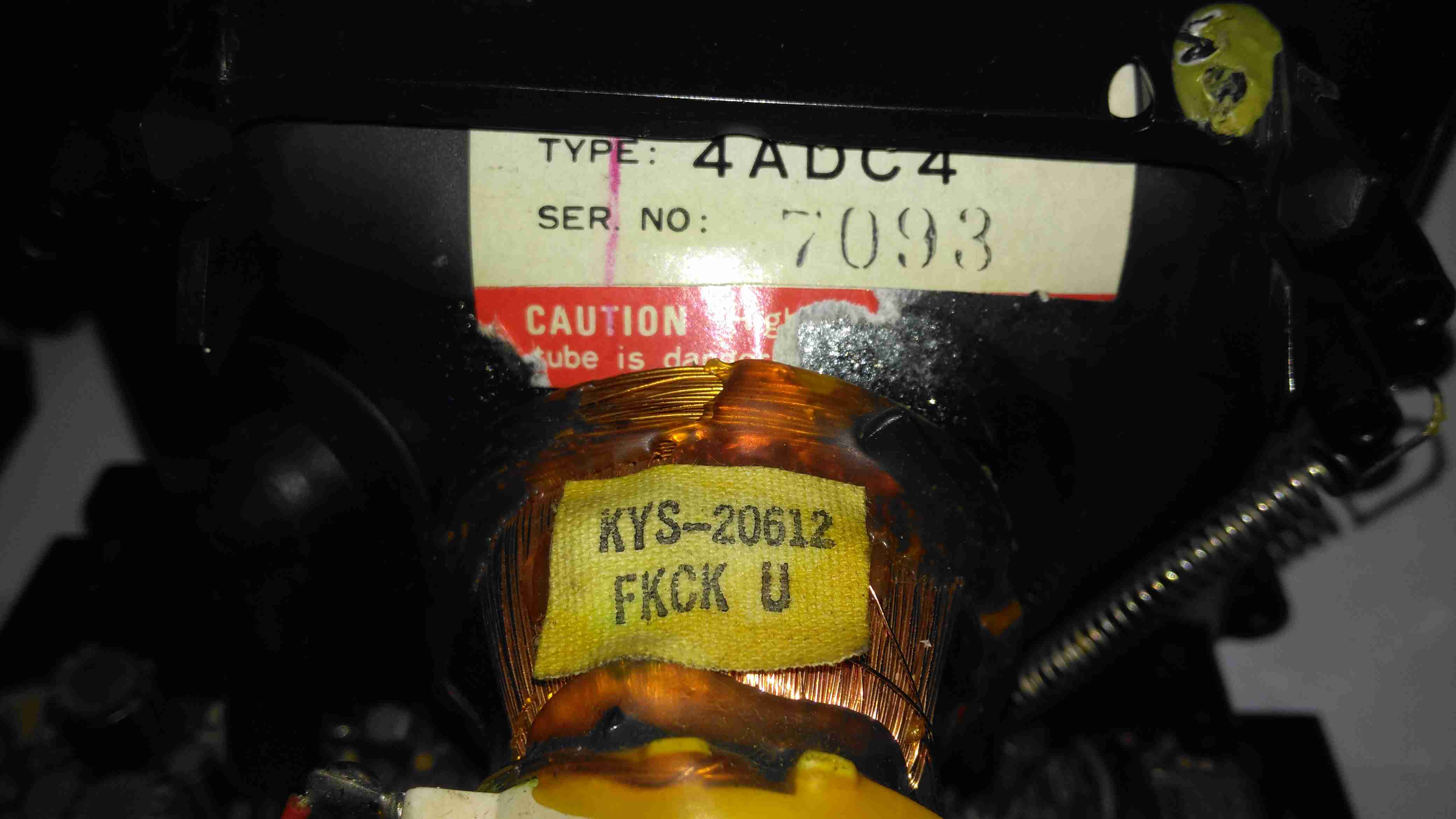
Tube Details
The CRT is a Samsung Electron Devices 4ADC4, with a really wide deflection angle. It’s a fair bit shorter than the Chinese CRT I have which is just a little larger, with a neck tube very thin indeed for the overall tube size.
Unusually, while the filament voltage is derived from the flyback transformer as usual, it’s rectified into DC in this unit, passing through a 1Ω resistor before the filament connection. I measured 5.3v here. The glow from the filament is barely visible even in the dark.
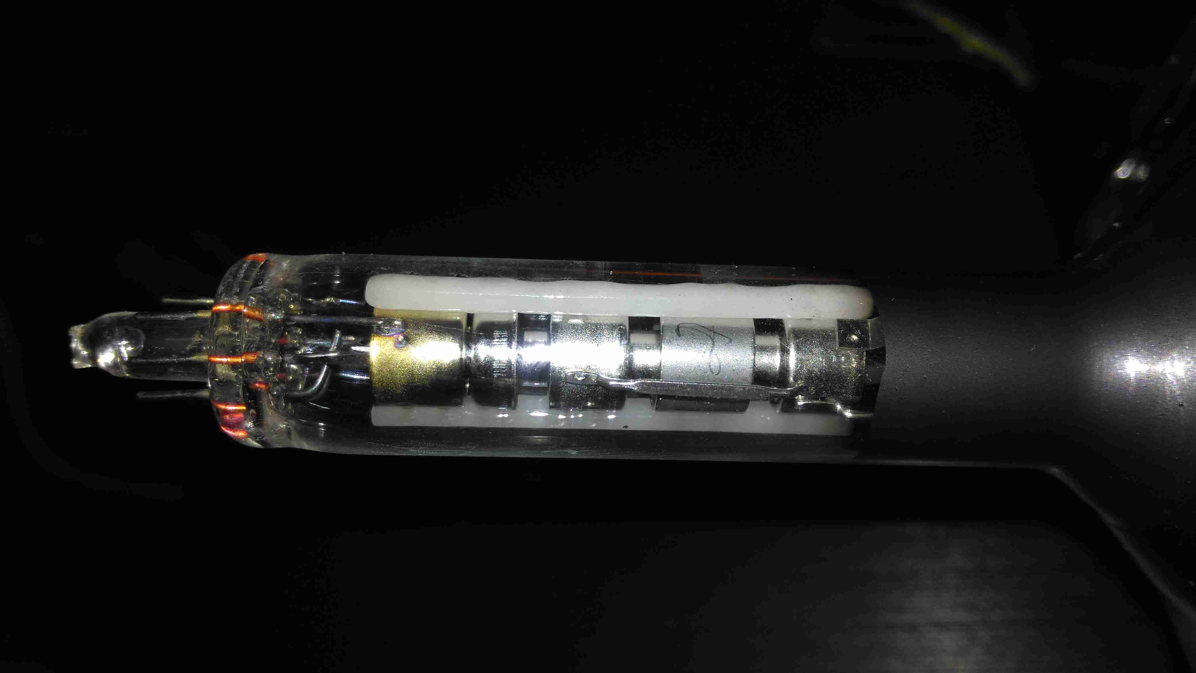
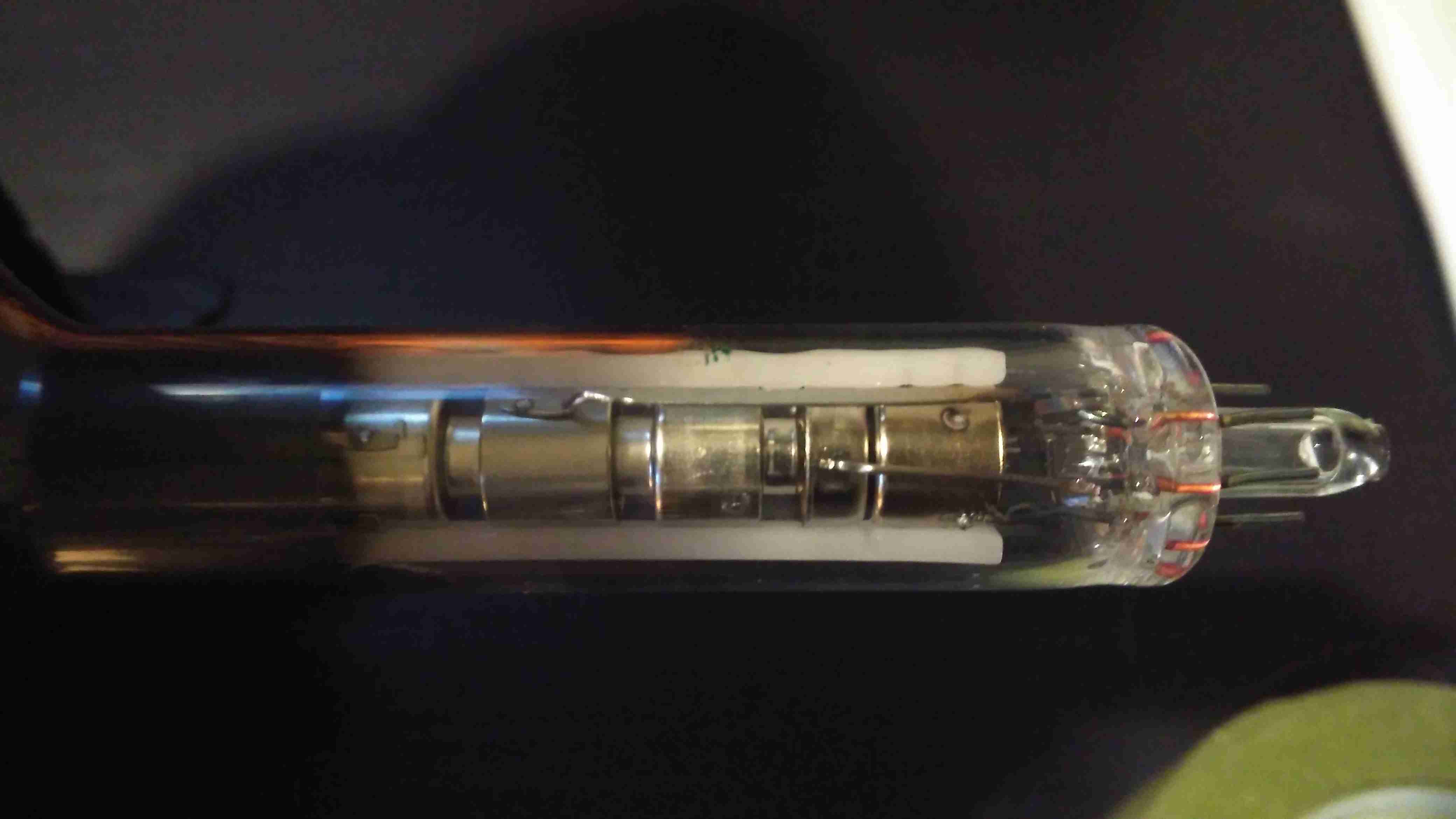
Electron Gun 1
The electron gun is the usual for a monochrome tube, with 7 pins on the seal end.
Electron Gun 2
The electrodes here from left are Final Anode, G3 (Focus Grid), Accelerating Anode, G2 (Screen Grid), G1 (Control Grid). The cathode & filament are hidden inside G1. In operation there’s about 250v on G2, and about 80v on G3.
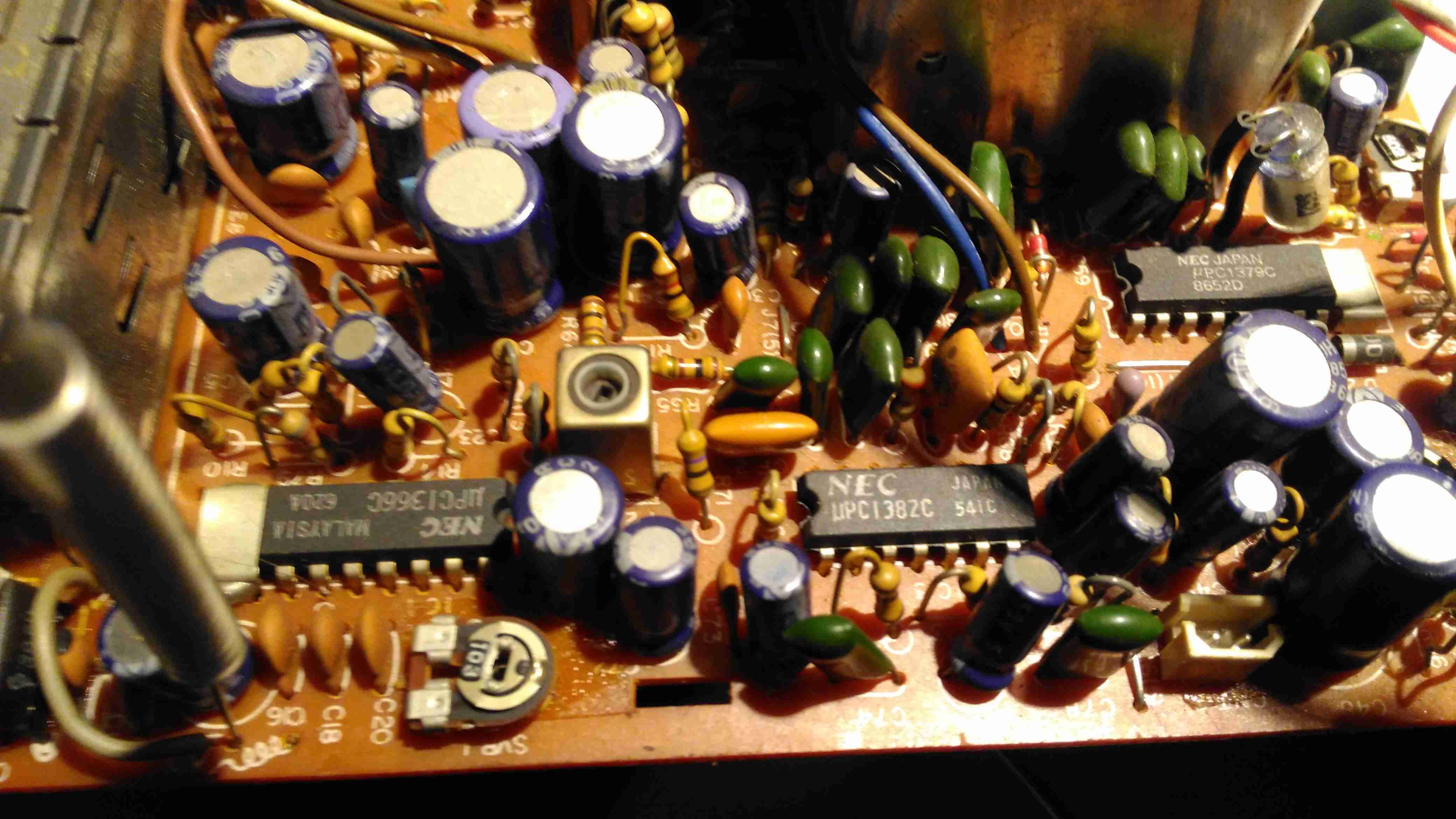
Chipset
The chipset used here is all NEC, starting with a µPC1366C Video IF Processor, which receives the IF signal from the tuner module to the left. This IC outputs the standard composite signal, and a modulated sound signal.
This then splits off to a µPC1382C Sound IF Processor & Attenuator IC, which feeds the resulting sound through the two pin header at the right bottom edge of the board to the audio amplifier in the chassis.
The composite video signal is fed through a discrete video amplifier with a single 2SC2229 transistor before going to the CRT cathode.
The remaining IC is a µPC1379C Sync Signal Processor, containing the sync separator, this is generating the required waveforms to drive the CRT deflection systems from another tap off the composite video line.
From this chip I can assume the unit was built around 1986, since this is the only date code on any of the semiconductors. Besides these 3 ICs, the rest of the circuit is all discrete components, which are well-crammed into the small board space.
There are 5 trimmer potentiometers on the board here, I’ve managed to work out the functions of nearly all of them:
SVR1: IF Gain Adjust
SVR2: H. Hold
SVR3: V. Size
SVR4: B+ Voltage Adjust
SVR5: Tuner Frequency Alignment? It’s in series with the tuning potentiometer in the chassis.
PCB Bottom
The PCB bottom shows the curved track layout typical of a hand taped out board. The soldermask is starting to flake off in places due to age, and there a couple of bodge wires completing a few ground traces. Respinning a board in those days was an expensive deal! Surprisingly, after all this time I’ve found no significant drift in the fixed resistors, but the carbon track potentiometers are drifiting significantly – 10KΩ pots are measuring as low as 8KΩ out of circuit. These will have to be replaced with modern versions, since there are a couple in timing-sensitive places, like the vertical & horizontal oscillator circuits.
Anode Cap Replaced
Here the anode cap has been replaced with a better silicone one from another TV. This should help keep the 6kV on the CRT from making an escape. This was an easy fix – pulling the contact fork out of the cap with it’s HT lead, desoldering the fork & refitting with the new cap in place.
Here I’ve replaced the important trimmers with new ones. Should help stabilize things a little.
Composite Injection Mod
Injecting a video signal is as easy as the other units. Pin 3 of the µPC1366C Video IF Processor is it’s output, so the track to Pin 3 is cut and a coax is soldered into place to feed in an external signal.
CRT In Operation
After hooking up a Raspberry Pi, we have display! Not bad after having stood idle for 30+ years.
Datasheets for the important ICs are available below:
[download id=”5690″]
[download id=”5693″]
[download id=”5696″]
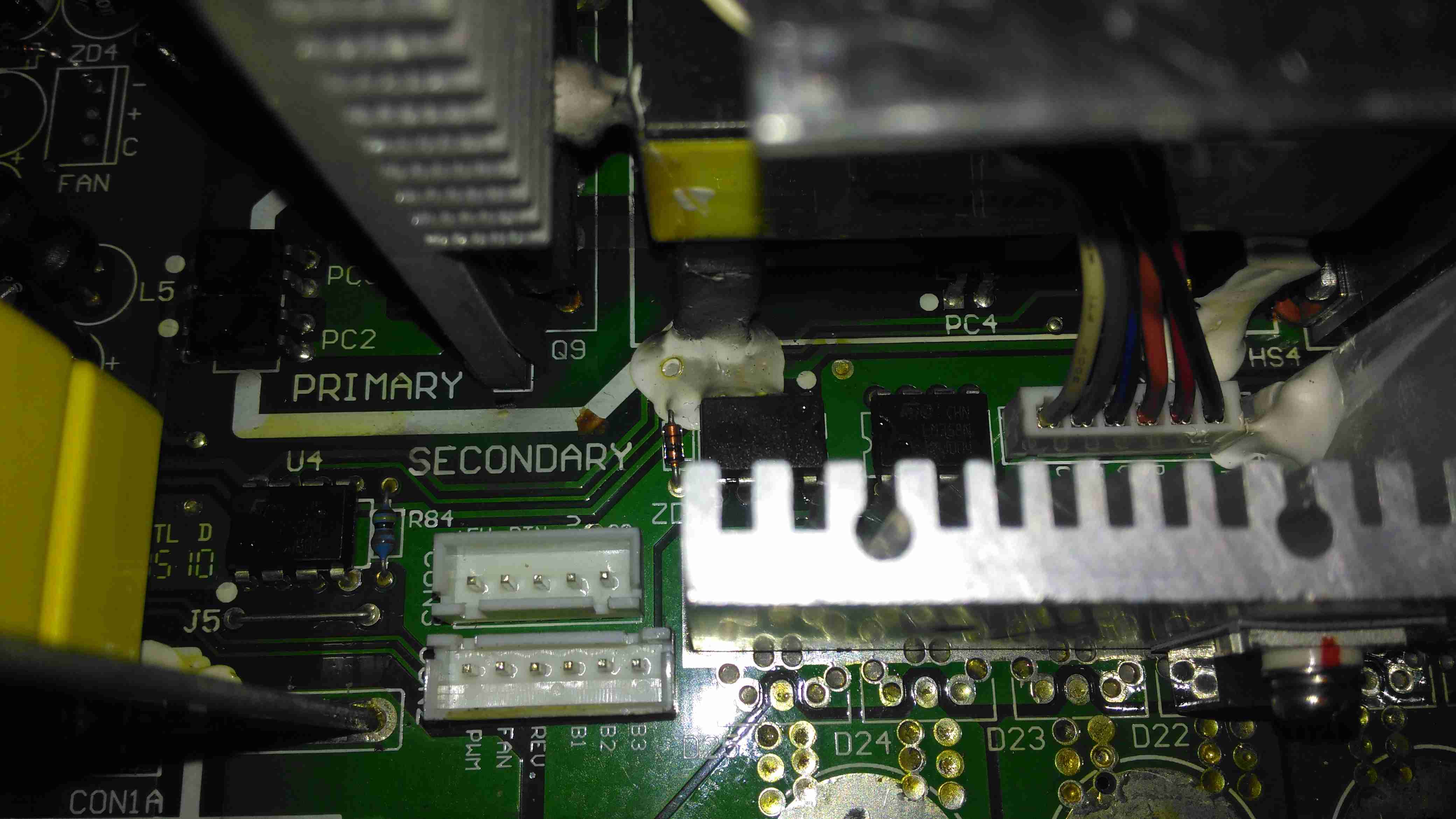
The Sterling charger we’ve had on board nb Tanya Louise since Feb 2014 has bitten the dust, with 31220 hours on it’s internal clock. Since we’re a liveaboard boat, this charger has had a lot of use while we’re on the mooring during winter, when the solar bank isn’t outputting it’s full rate. First, a bit of a teardown to explore the unit, then onto the repair:
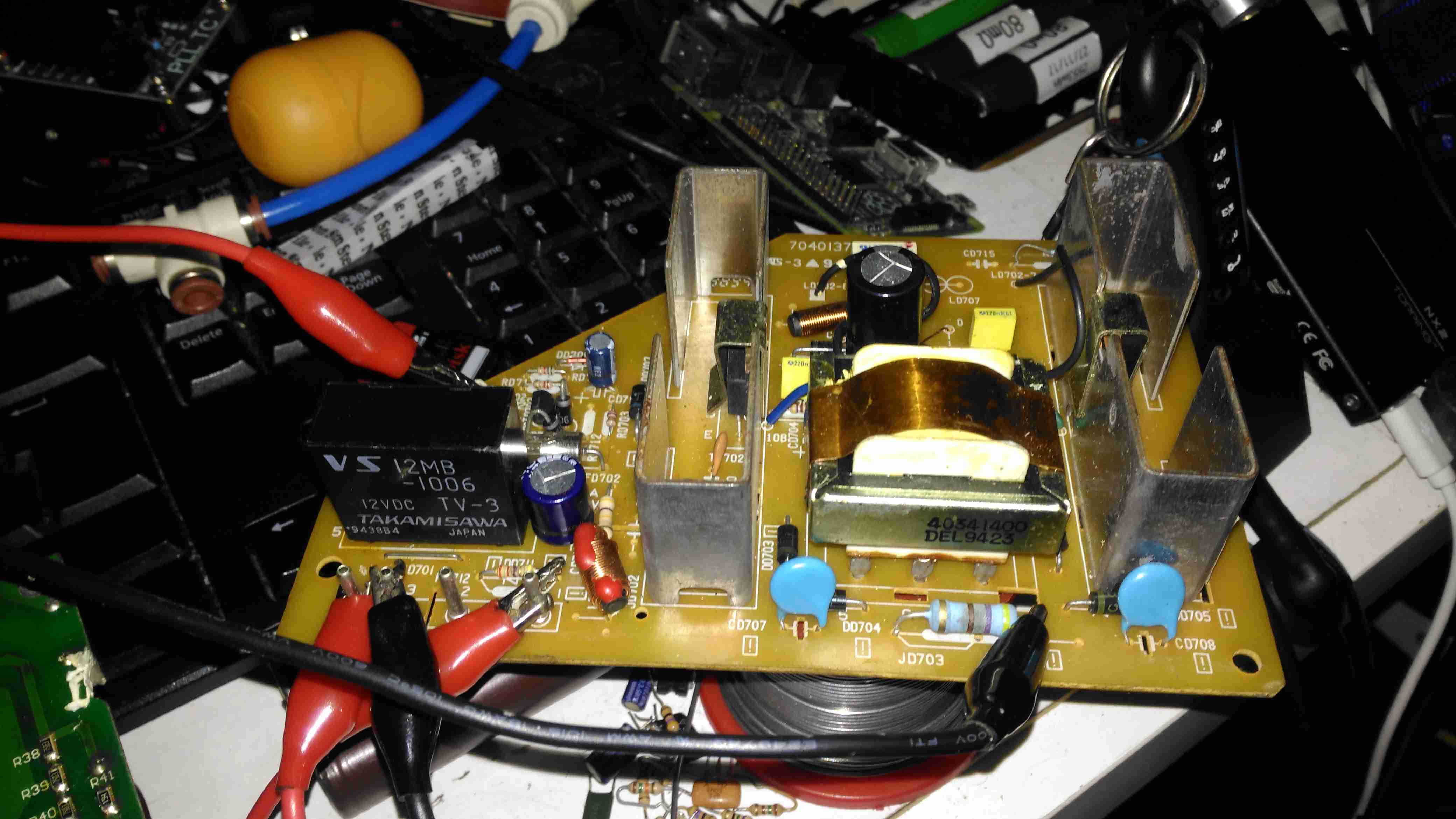
Active PFC Section
There’s the usual mains input filtering on the left, with the bridge rectifier on it’s heatsink.
Underneath the centre massive heatsinks is the main transformer (not visible here) & active PFC circuit. The device peeking out from underneath is the huge inductor needed for PFC. It’s associated switching MOSFET is to the right.
Logic PSU Section
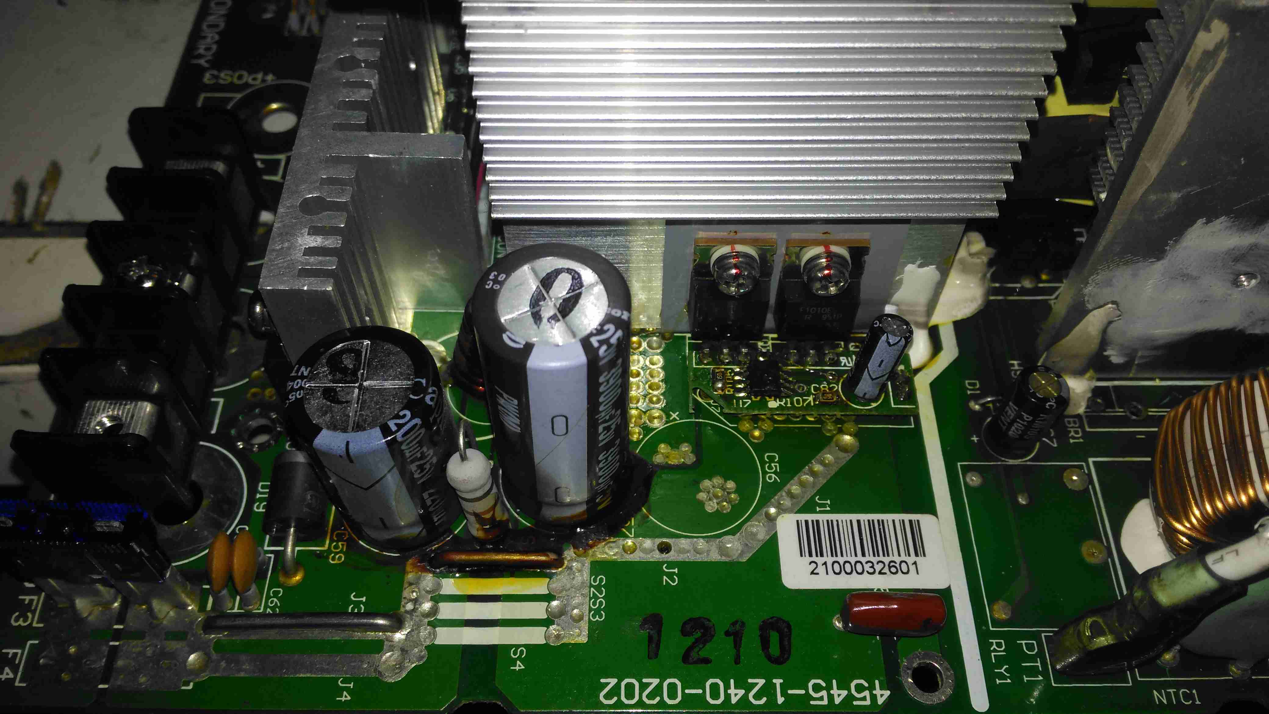
On the other side of the PFC section is the main DC rail filter electrolytic, a 450v 150µF part. Here some evidence of long-term heating can be seen in the adhesive around the base, it’s nearly completely turned black! It’s not a decent brand either, a Chinese CapXon.
The PCB fuse just behind it is in the DC feed to the main switching supply, so the input fuse only protects the filter & Active PFC circuitry. Luckily this fuse didn’t blow during the failure, telling me the fault was earlier in the power chain.
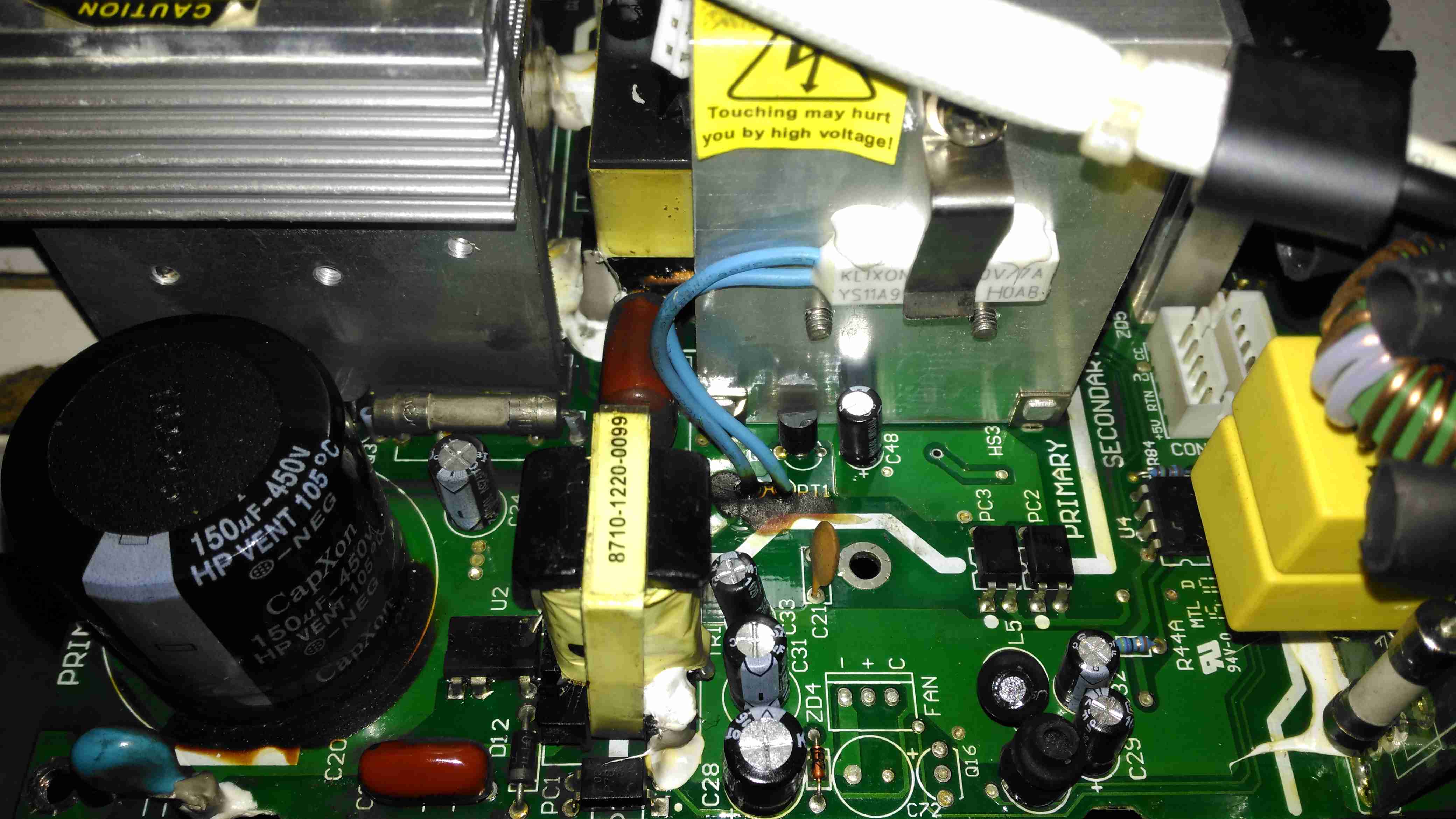
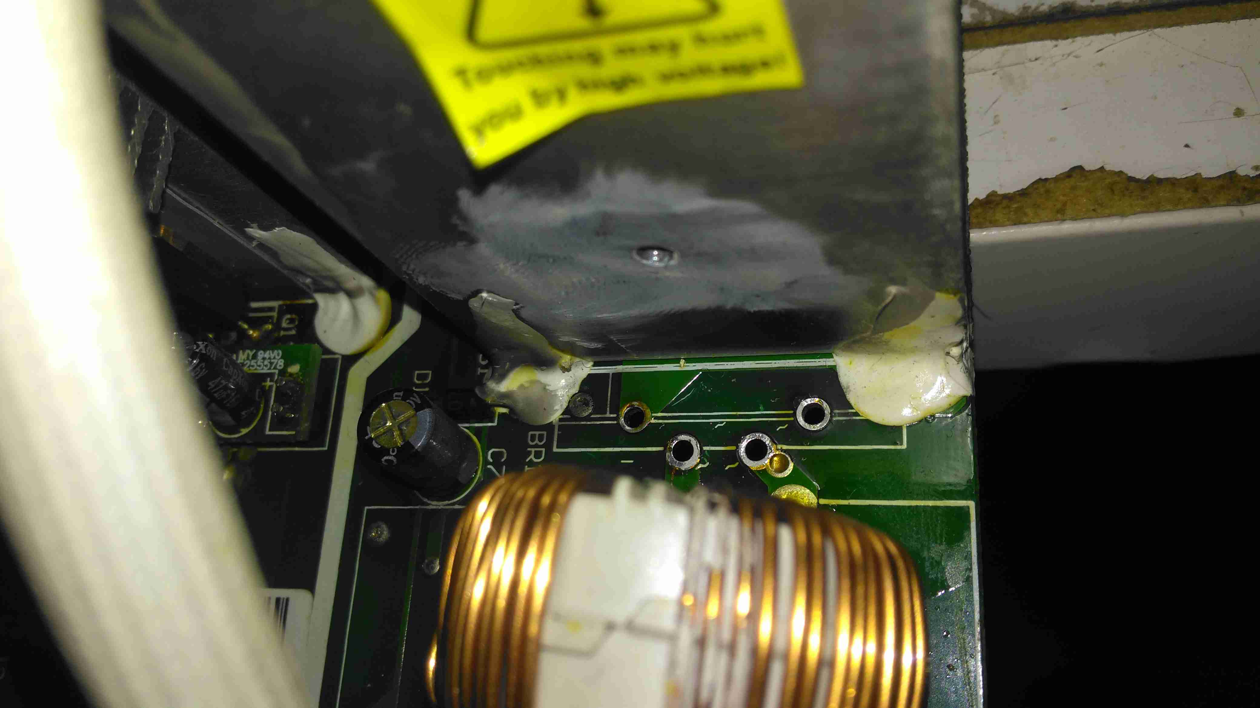
The logic circuits are powered by an independent switching supply in the centre, providing a +5v rail to the microcontroller. The fan header & control components are not populated in this 10A model, but I may end up retrofitting a fan anyway as this unit has always run a little too warm. The entire board is heavily conformal coated on both sides, to help with water resistance associated with being in a marine environment. This has worked well, as there isn’t a single trace of moisture anywhere, only dust from years of use.
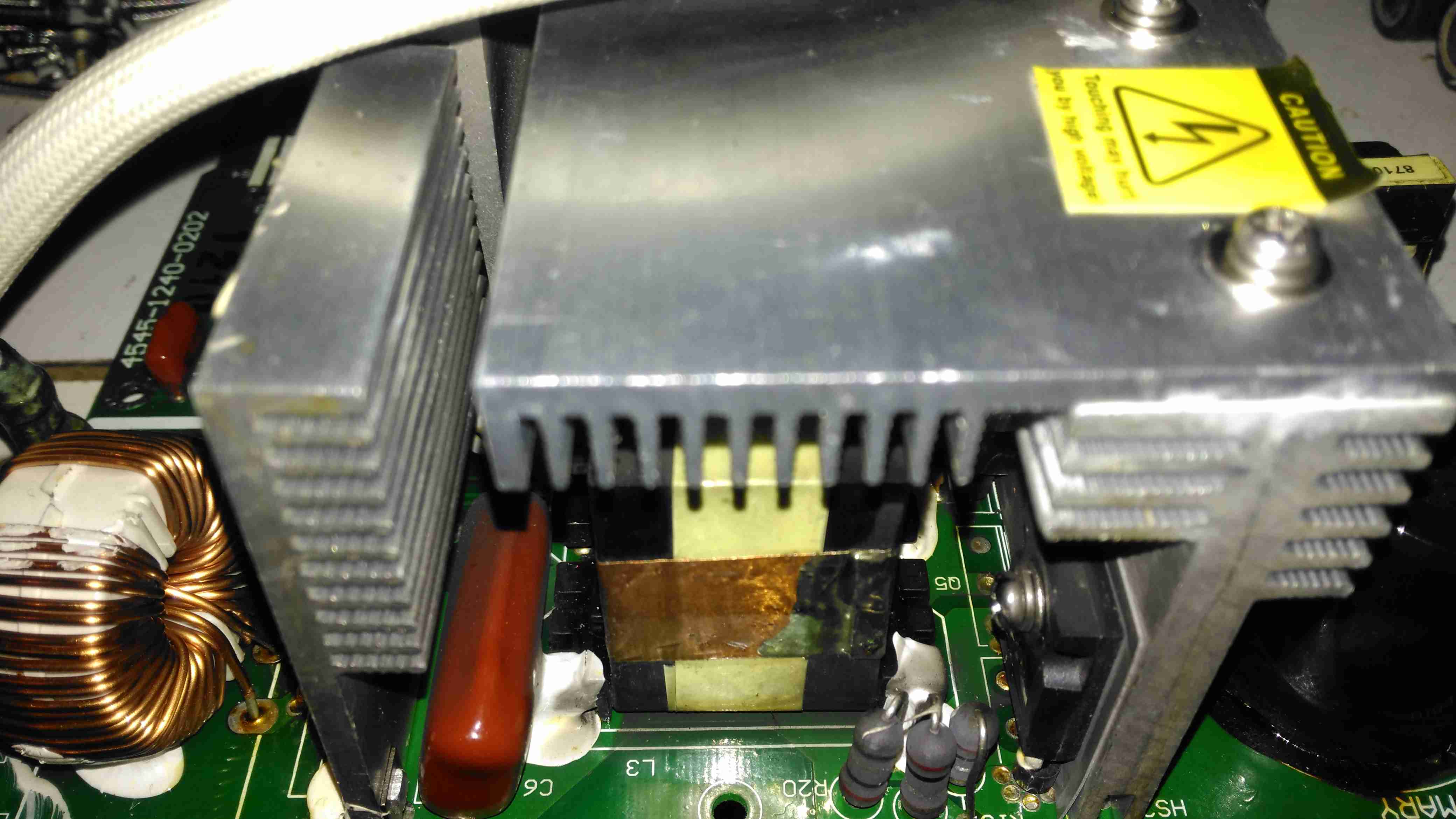
There is some thermal protection for the main SMPS switching MOSFETS with the Klixon thermal fuse clipped to the heatsink.
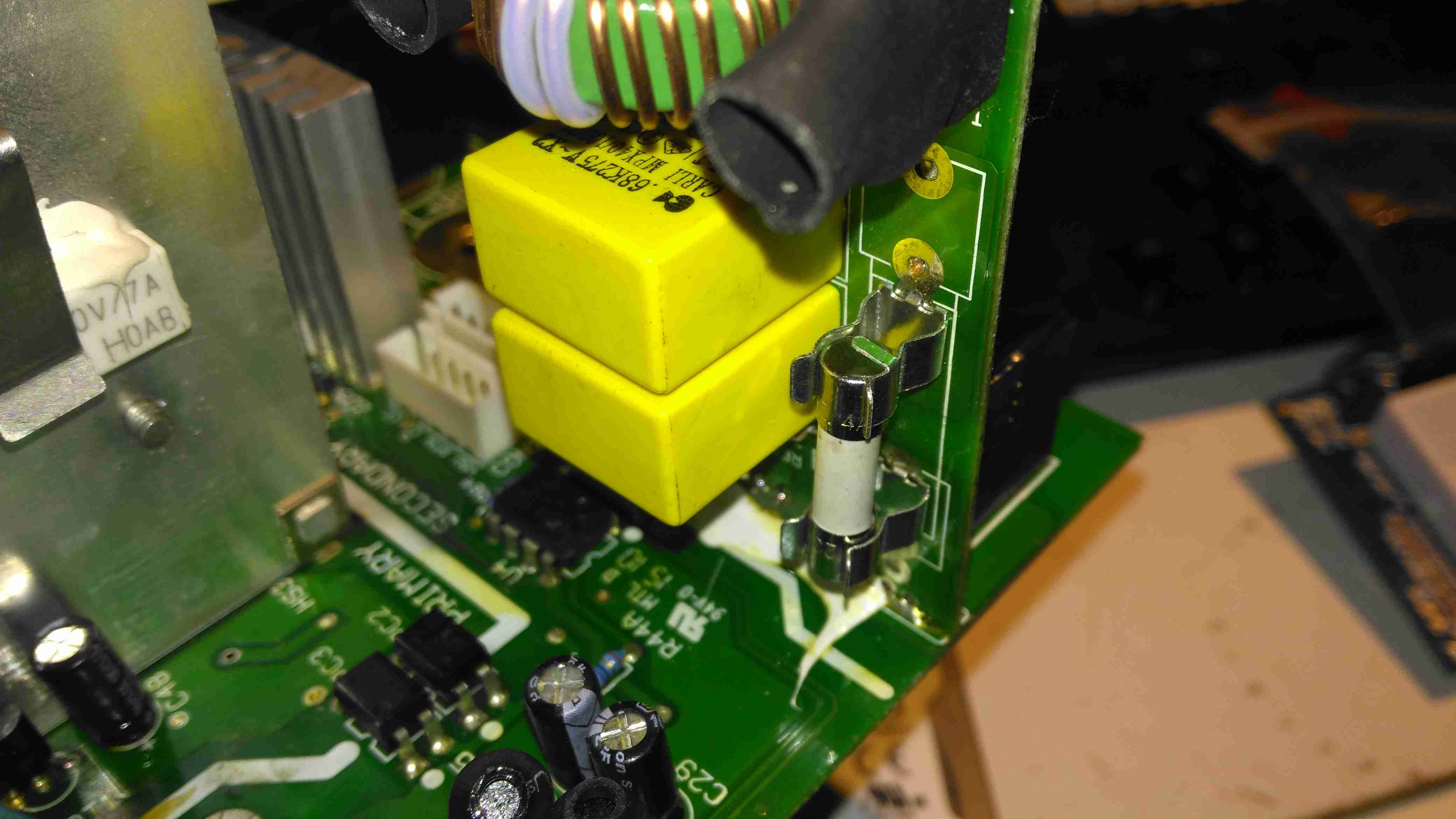
DC Output Section
The DC output rectifiers are on the large heatsink in the centre, with a small bodge board fitted. Due to the heavy conformal coating on the board I can’t get the ID from this small 8-pin IC, but from the fact that the output rectifiers are in fact IRF1010E MOSFETS, rated at 84A a piece, this is an synchronous rectifier controller.
Oddly, the output filter electrolytics are a mix of Nichicon (nice), and CapXon (shite). A bit of penny pinching here, which if a little naff since these chargers are anything but cheap. (£244.80 at the time of writing).
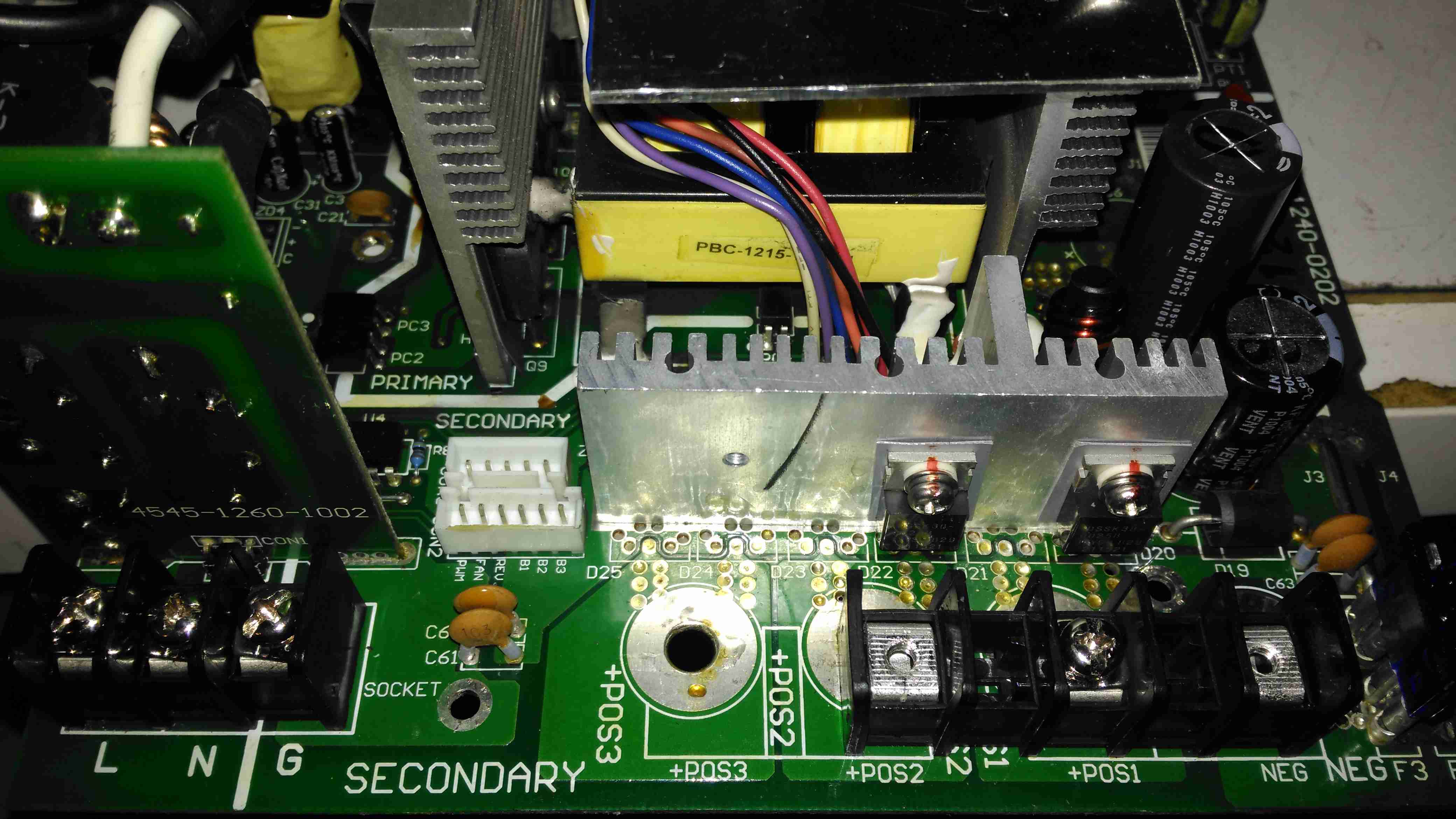
Hiding just behind the electrolytics is a large choke, and a reverse-polarity protection diode, which is wired crowbar-style. Reversing the polarity here will blow the 15A DC bus fuse instantly, and may destroy this diode if it doesn’t blow quick enough.
DC Outputs
Right on the output end are a pair of large Ixys DSSK38 TO220 Dual 20A dual Schottky diodes, isolating the two outputs from each other, a nice margin on these for a 10A charger, since the diodes are paralleled each channel is capable of 40A. This prevents one bank discharging into another & allows the charger logic to monitor the voltages individually. The only issue here is the 400mV drop of these diodes introduce a little bit of inefficiency. To increase current capacity of the PCB, the aluminium heatsink is being used as the main positive busbar. From the sizing of the power components here, I would think that the same PCB & component load is used for all the chargers up to 40A, since both the PFC inductor & main power transformer are massive for a 10A output. There are unpopulated output components on this low-end model, to reduce the cost since they aren’t needed.
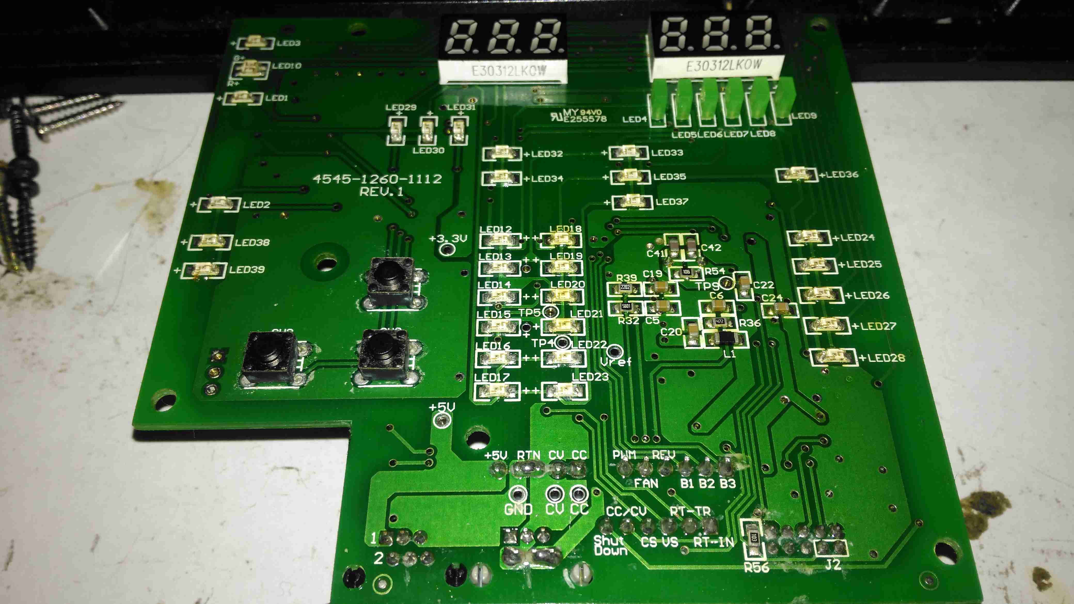
Front Panel Control Connections
A trio of headers connect all the control & sense signals to the front panel PCB, which contains all the control logic. This unit is sensing all output voltages, output current & PSU rail voltages.
Front Panel LEDs
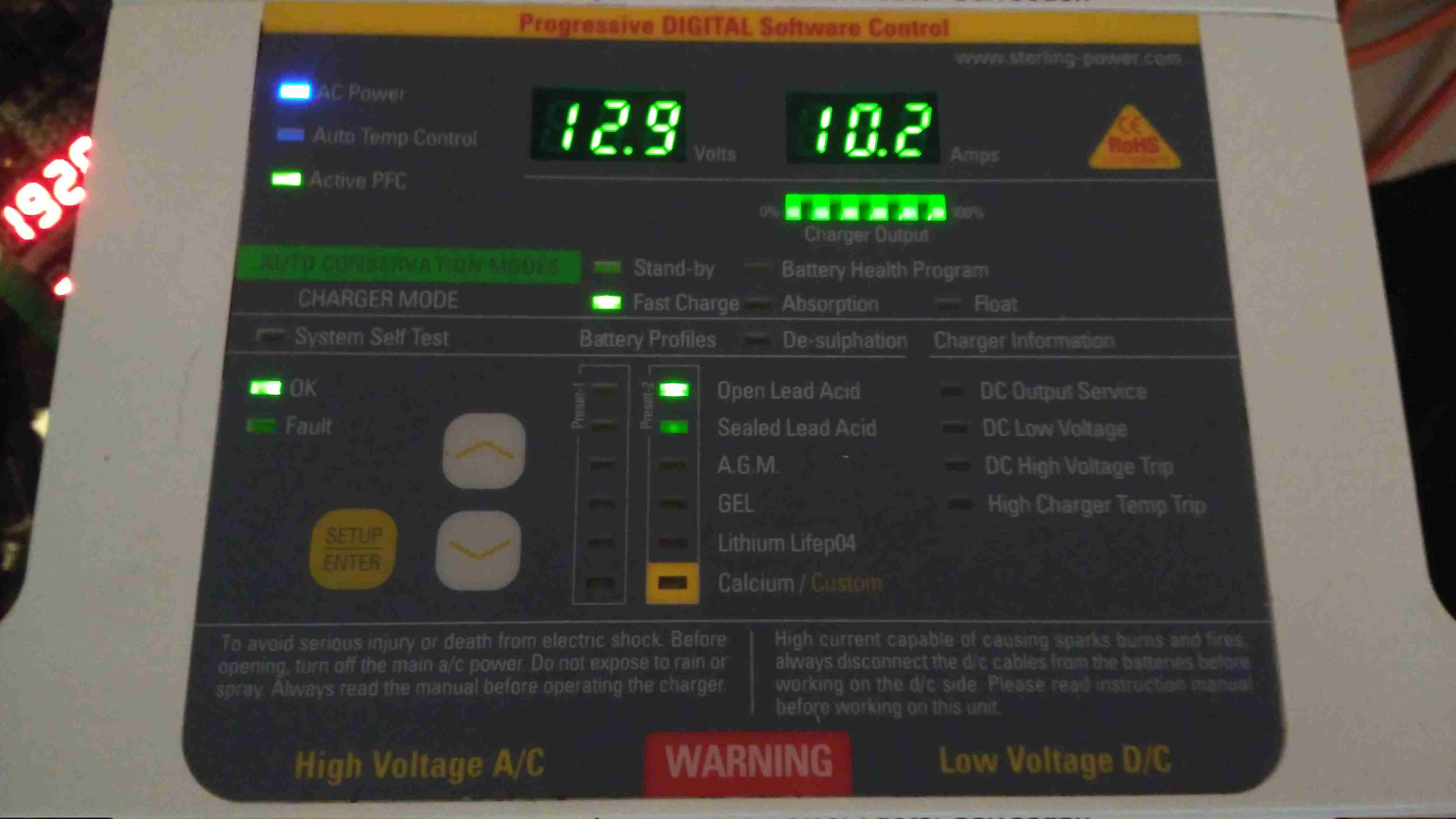
The front panel is stuffed with LEDs & 7-segment displays to show the current mode, charging voltage & current. There’s 2 tactile switches for adjustments.
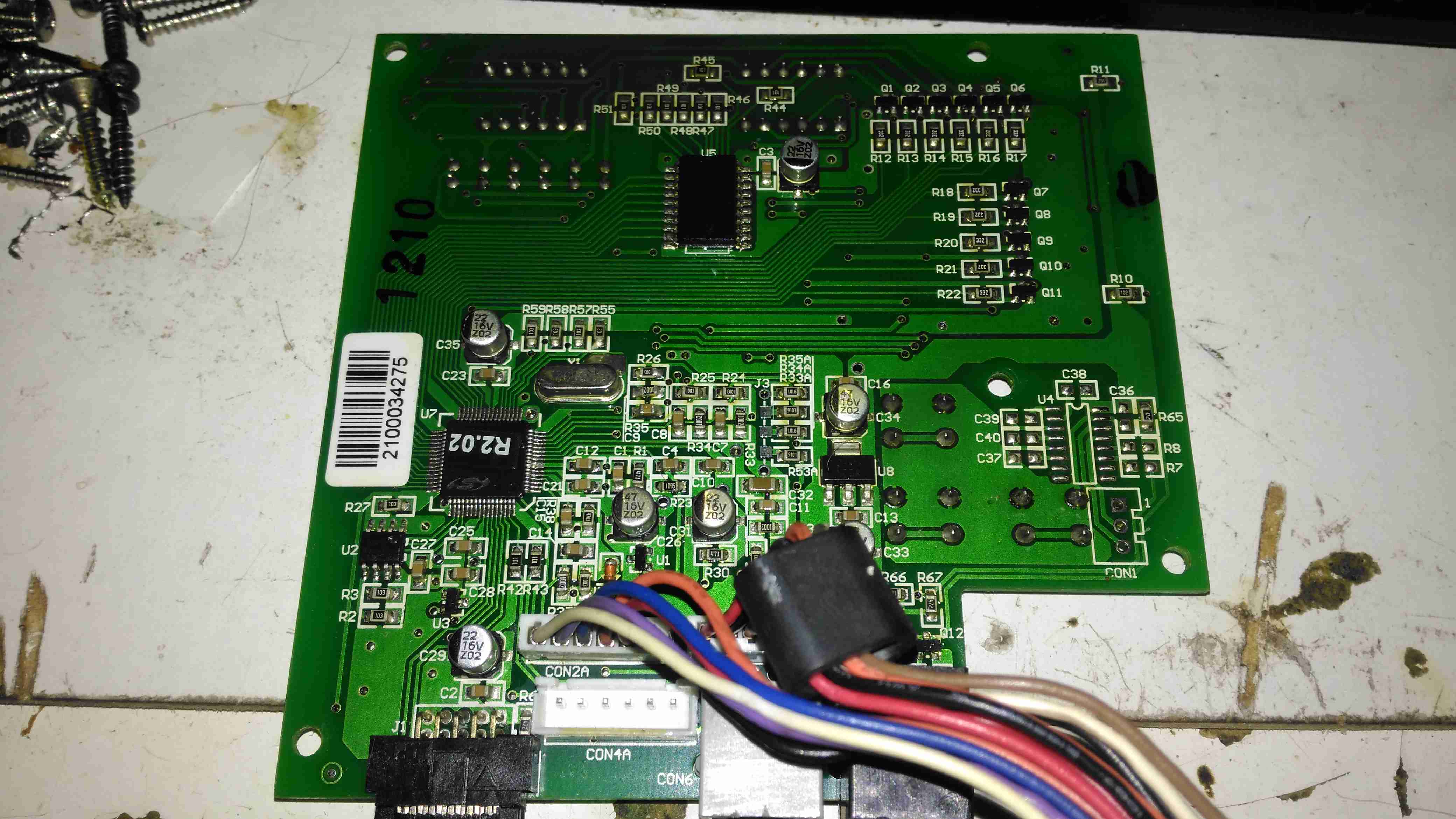
Front Panel Reverse
The reverse of the board has the main microcontroller – again identifying this is impossible due to the heavy conformal coat. The LEDs are being driven through a 74HC245D CMOS Octal Bus Transceiver.
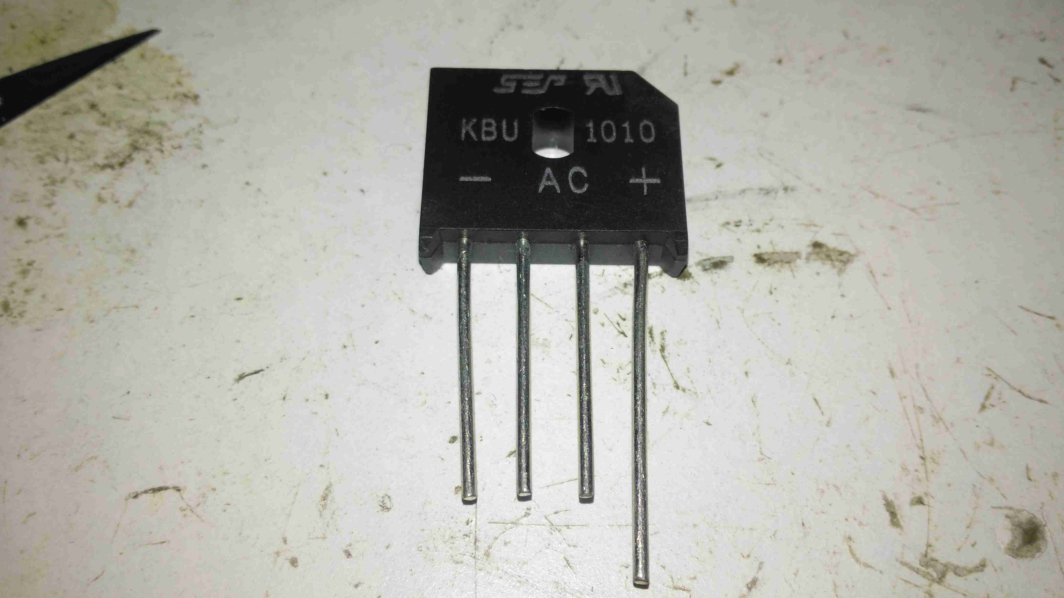
Now on to the repair! I’m not particularly impressed with only getting 4 years from this unit, they are very expensive as already mentioned, so I would expect a longer lifespan. The input fuse had blown in this case, leaving me with a totally dead charger. A quick multimeter test on the input stage of the unit showed a dead short – the main AC input bridge rectifier has gone short circuit.
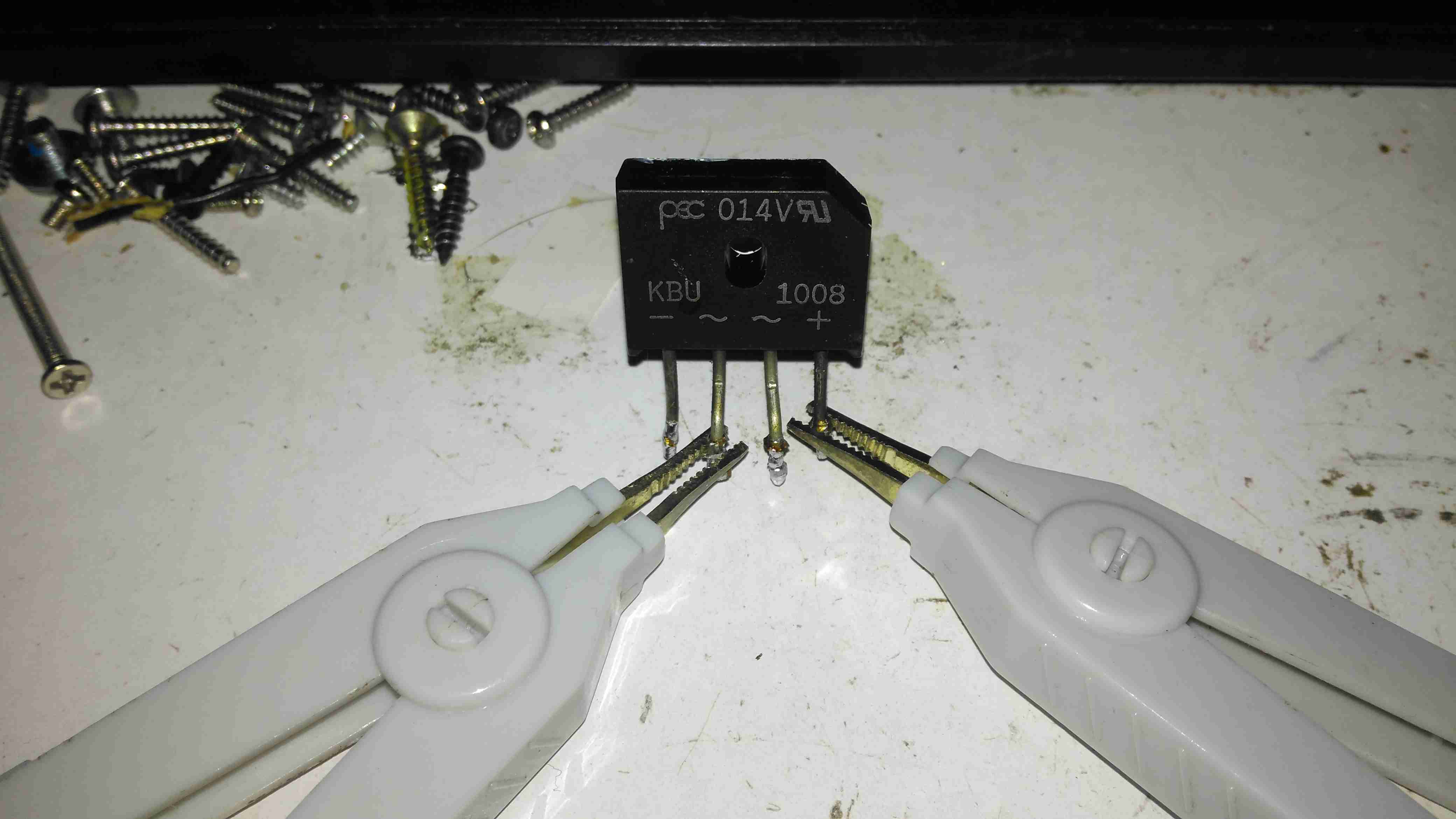
Bridge Rectifier Removed
Here the defective bridge has been desoldered from the board. It’s a KBU1008 10A 800v part. Once this was removed I confirmed there was no longer an input short, on either the AC side or the DC output side to the PFC circuit.
Testing The Rectifier
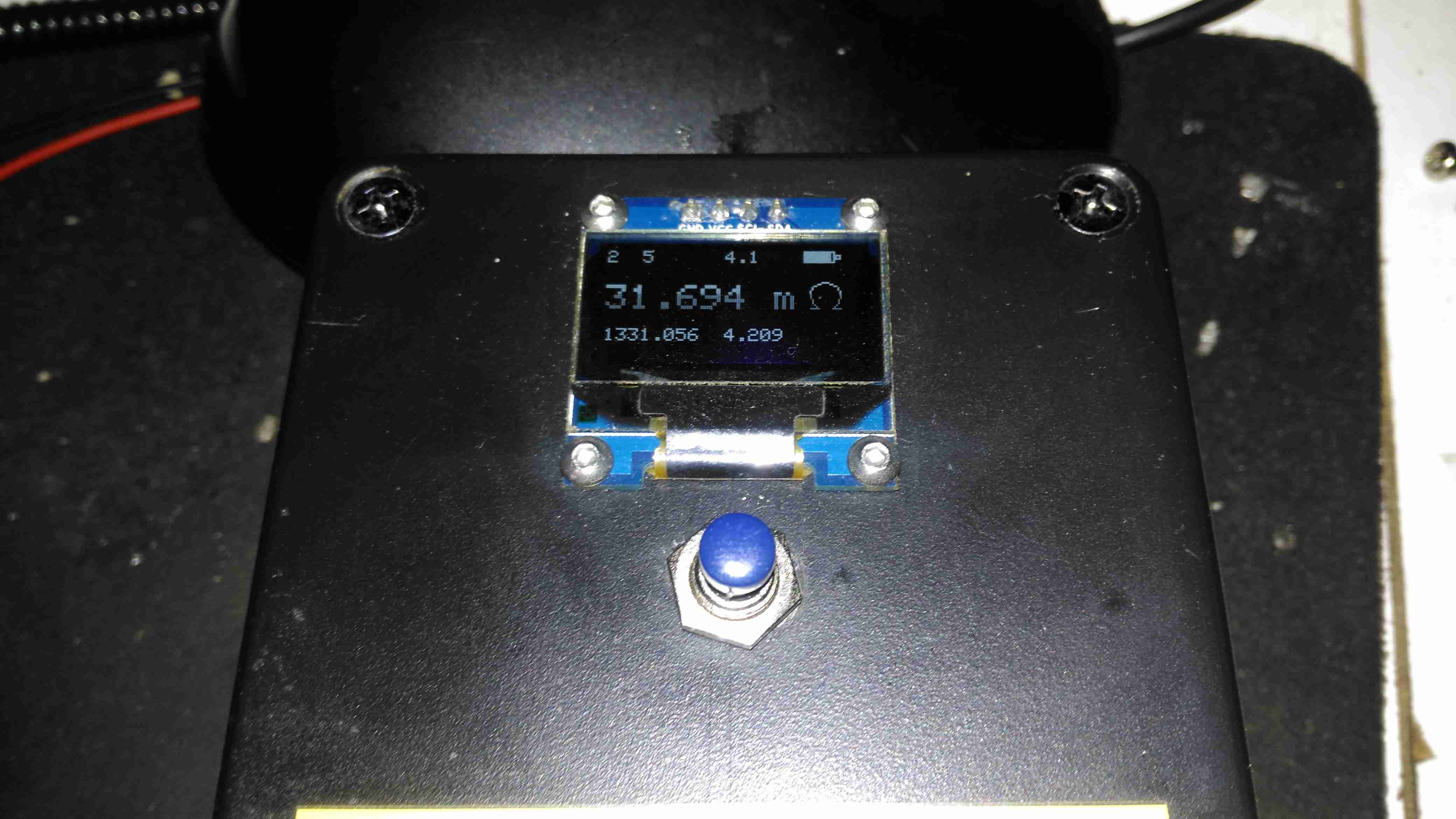
Time to stick the desoldered bridge on the milliohm meter & see how badly it has failed.
Yep, Definitely Shorted
I’d say 31mΩ would qualify as a short. It’s no wonder the 4A input fuse blew instantly. There is no sign of excessive heat around the rectifier, so I’m not sure why this would have failed, it’s certainly over-rated for the 10A charger.
Testing Without Rectifier
Now the defective diode bridge has been removed from the circuit, it’s time to apply some controlled power to see if anything else has failed. For this I used a module from one of my previous teardowns – the inverter from a portable TV.
Test Inverter
This neat little unit outputs 330v DC at a few dozen watts, plenty enough to power up the charger with a small load for testing purposes. The charger does pull the voltage of this converter down significantly, to about 100v, but it still provides just enough to get things going.
It’s Alive!
After applying some direct DC power to the input, it’s ALIVE! Certainly makes a change from the usual SMPS failures I come across, where a single component causes a chain reaction that writes off everything.
Replacement Rectifier
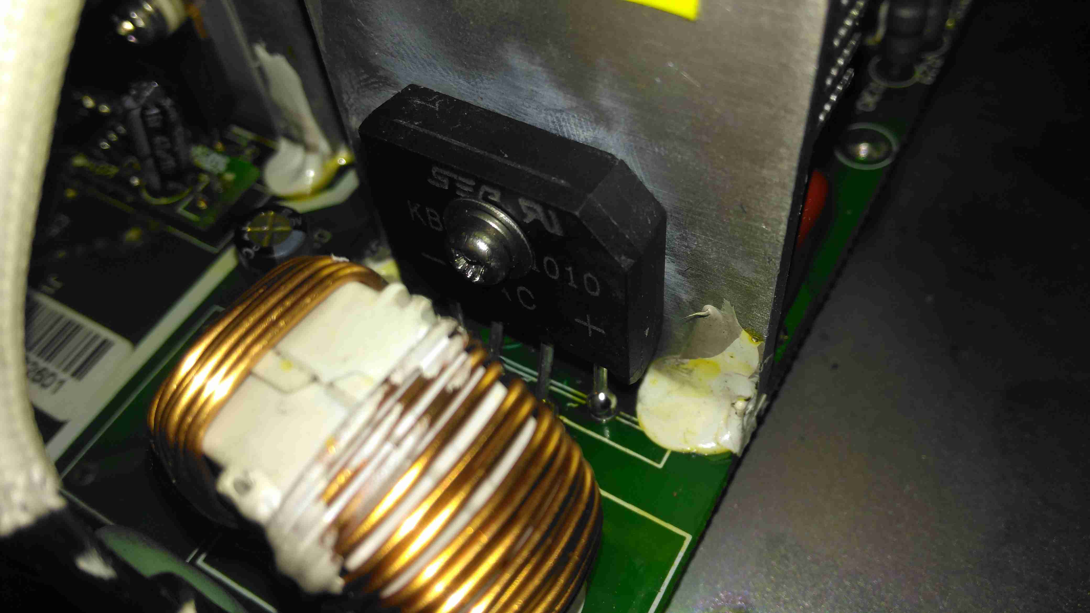
Unfortunately I couldn’t find the exact same rectifier to replace the shorted one, so I had to go for the KBU1010, which is rated for 1000v instead of 800v, but the Vf rating (Forward Voltage), is the same, so it won’t dissipate any more power.
Soldered In
Here’s the new rectifier soldered into place on the PCB & bolted to it’s heatsink, with some decent thermal compound in between.
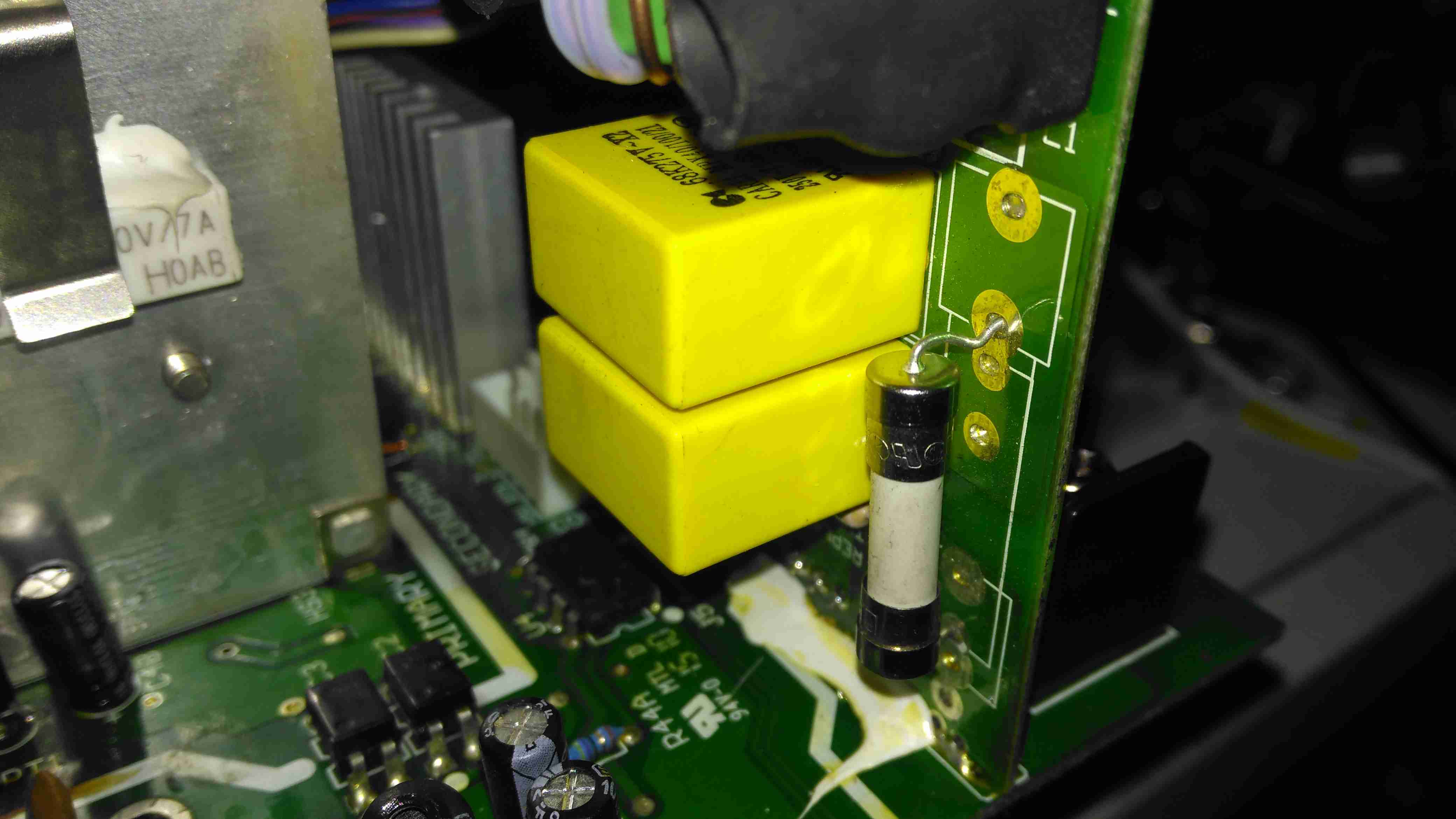
Input Board
Here is the factory fuse, a soldered in device. I’ll be replacing this with standard clips for 20x5mm fuses to make replacement in the future easier, the required hole pattern in the PCB is already present. Most of the mains input filtering is also on this little daughterboard.
Fuse Replaced
Now the fuse has been replaced with a standard one, which is much more easily replaceable. This fuse shouldn’t blow however, unless another fault develops.
Full Load Test
Now everything is back together, a full load test charging a 200Ah 12v battery for a few hours will tell me if the fix is good. This charger won’t be going back into service onboard the boat, it’s being replaced anyway with a new 50A charger, to better suit the larger loads we have now. It won’t be a Sterling though, as they are far too expensive. I’ll report back if anything fails!
Here’s the MT50 controller from EpEver, that interfaces with it’s Tracer MPPT solar charge controllers, and gives access to more programming options on the charge controllers, without the need for a laptop. The display is a large dot-matrix unit, with built in backlight. Above is the display on the default page, showing power information for the entire system.
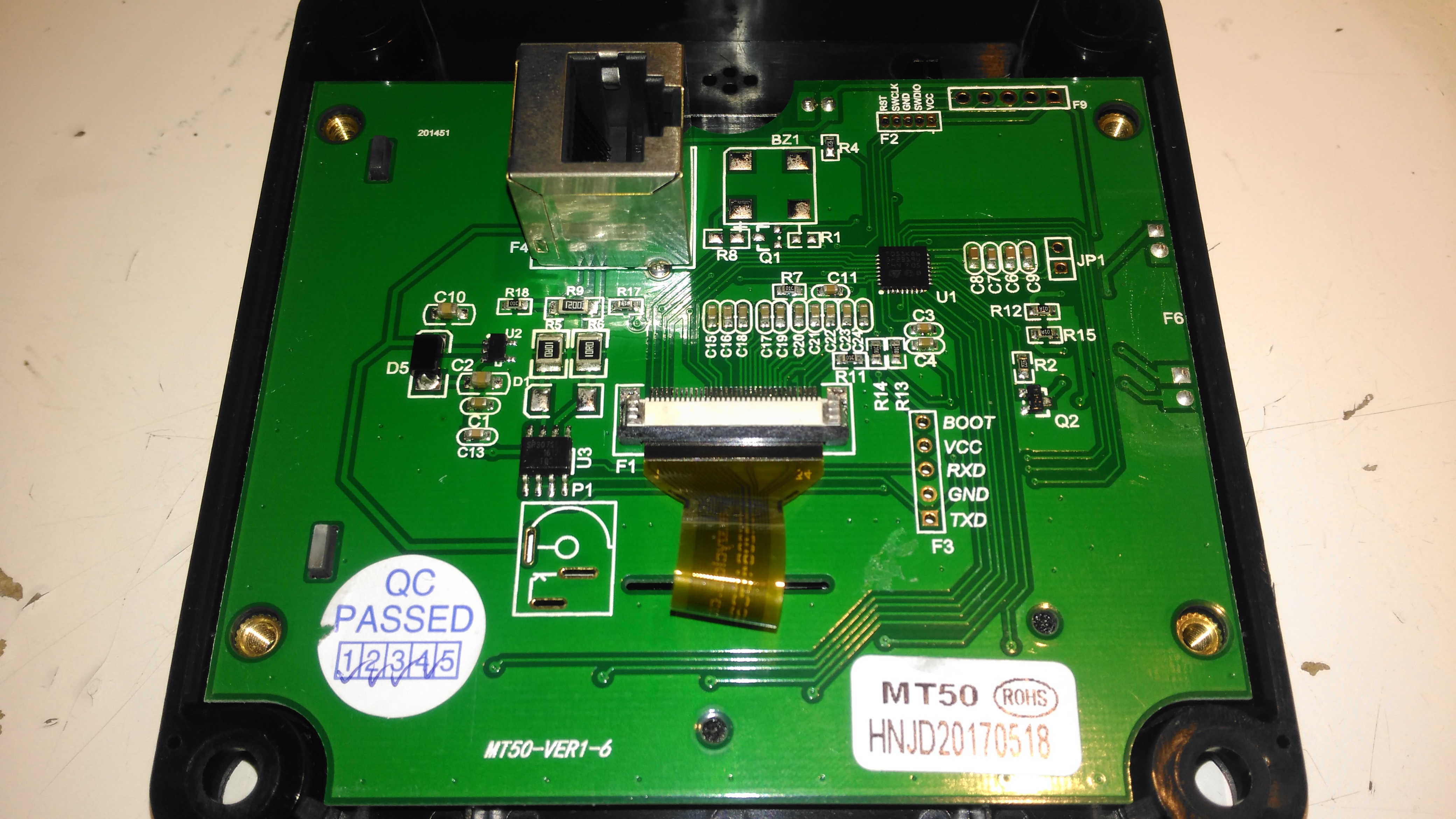
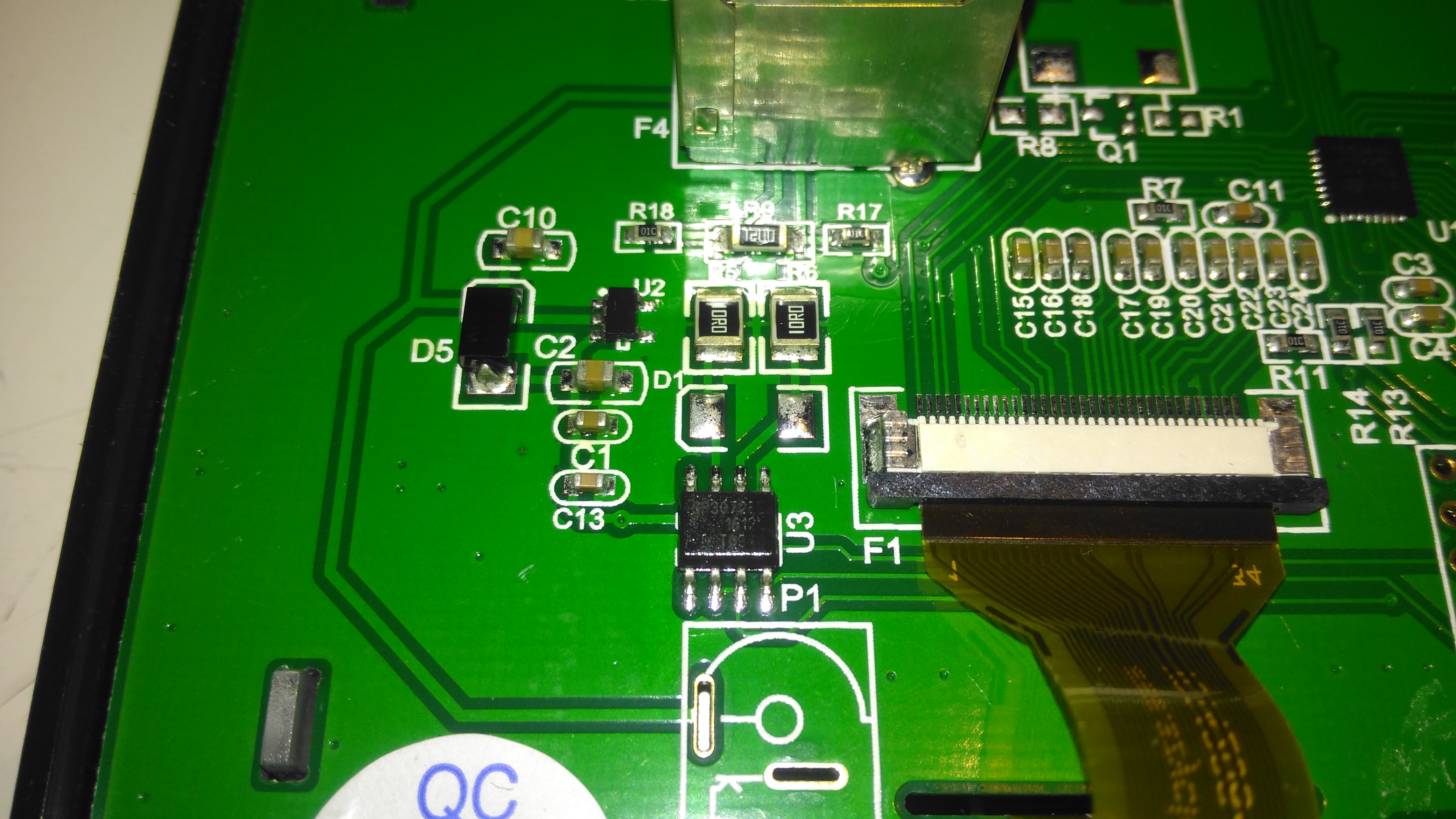
PCB Rear
The rear plastic cover is held in place by 4 machine screws, which thread into brass inserts in the plastic frame – nice high quality touch on the design here, no cheap self tapping plastic screws. Both power & data arrive via an Ethernet cable, but the communication here is RS-485, and not compatible with Ethernet! The PCB is pretty sparse, with comms & power on the left, LCD connection in the centre, and the microcontroller on the right.
RS-485 Transceiver
On the left of the board is the RS0485 transceiver, and a small voltage regulator. There’s also a spot for a DC barrel jack, which isn’t included in this model for local power supply.
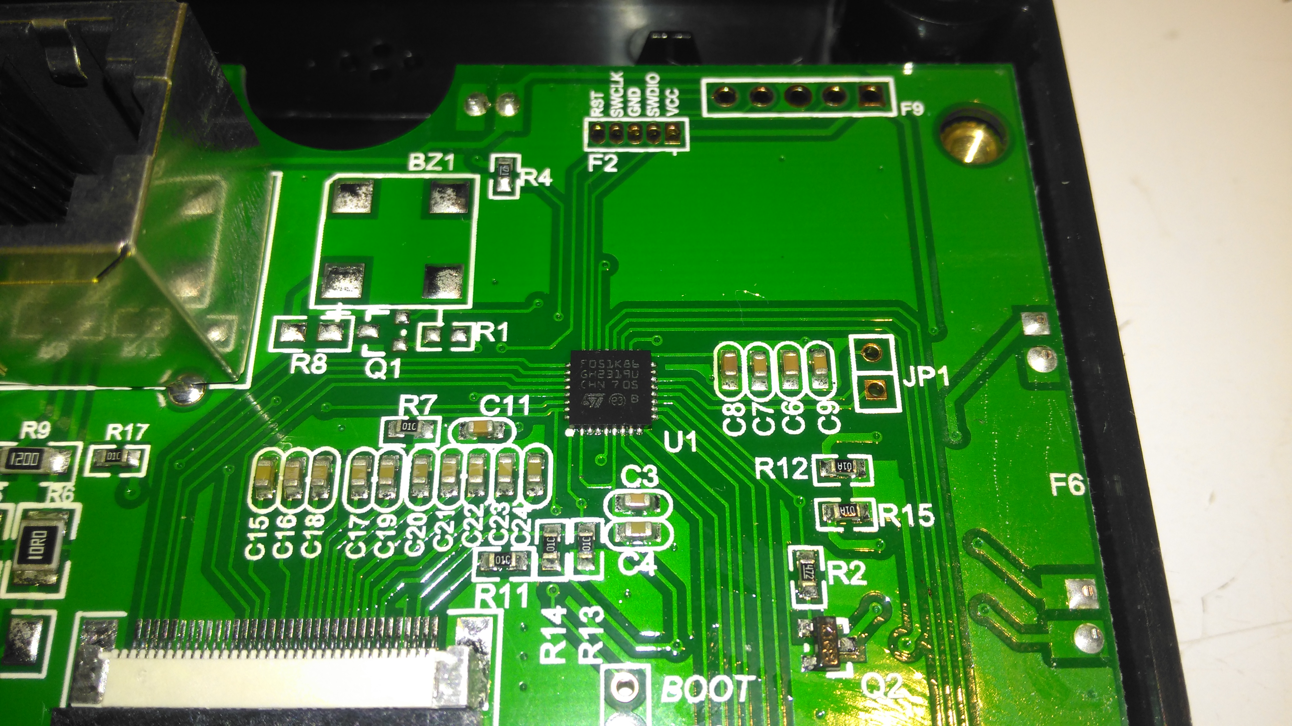
STM32 Microcontroller
The other side of the board holds the main microcontroller which communicates with the charge controller. This is a STM32F051K8 from ST Microelectronics. With a 48MHz ARM Cortex M0 core, and up to 64K of flash, this is a pretty powerful MCU that has very little to do in this application.
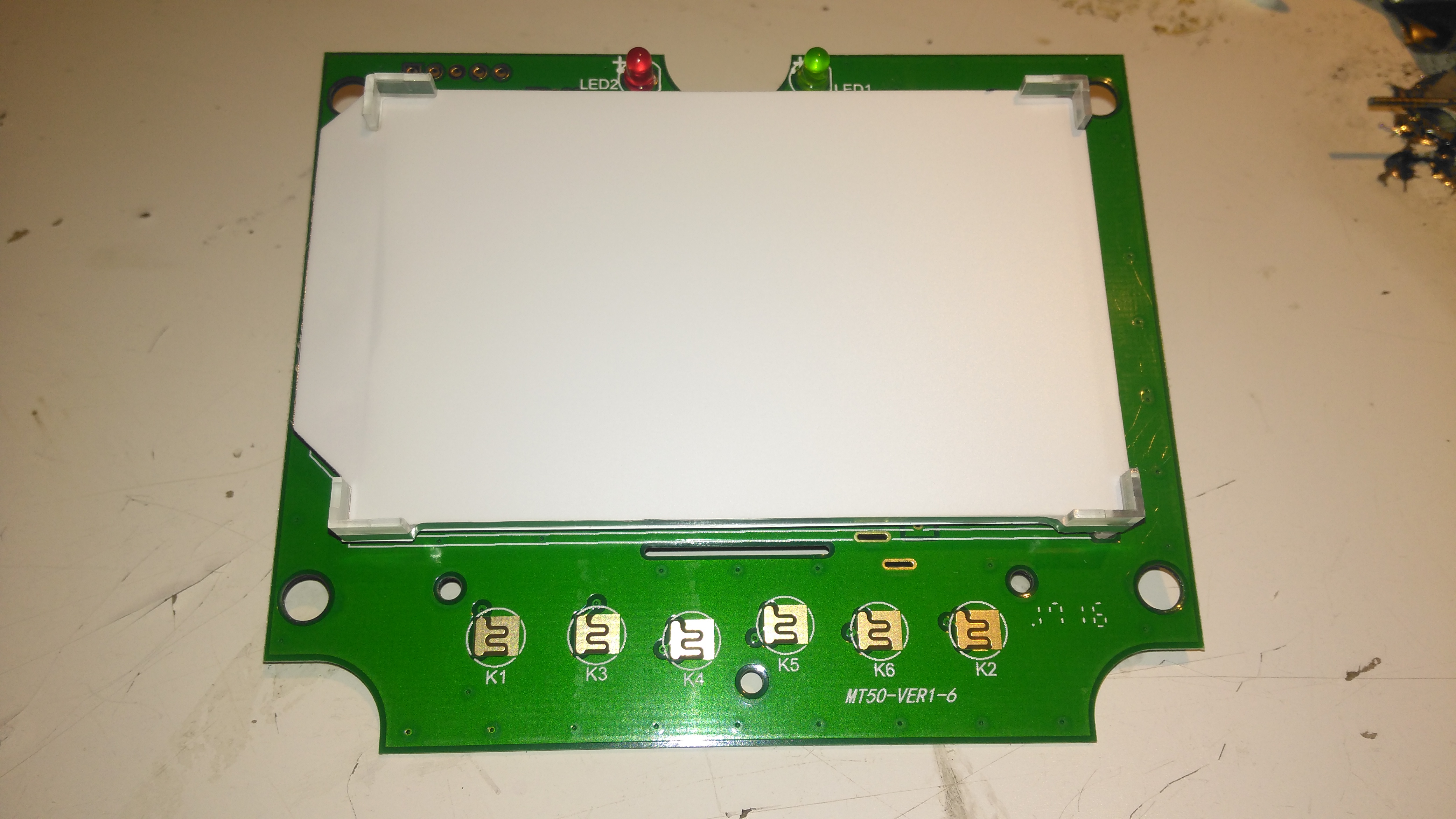
PCB Front
The front of the PCB has the ENIG contacts of the front panel buttons, and the LCD backlight assembly. There’s nothing else under the plastic backlight spreader either.
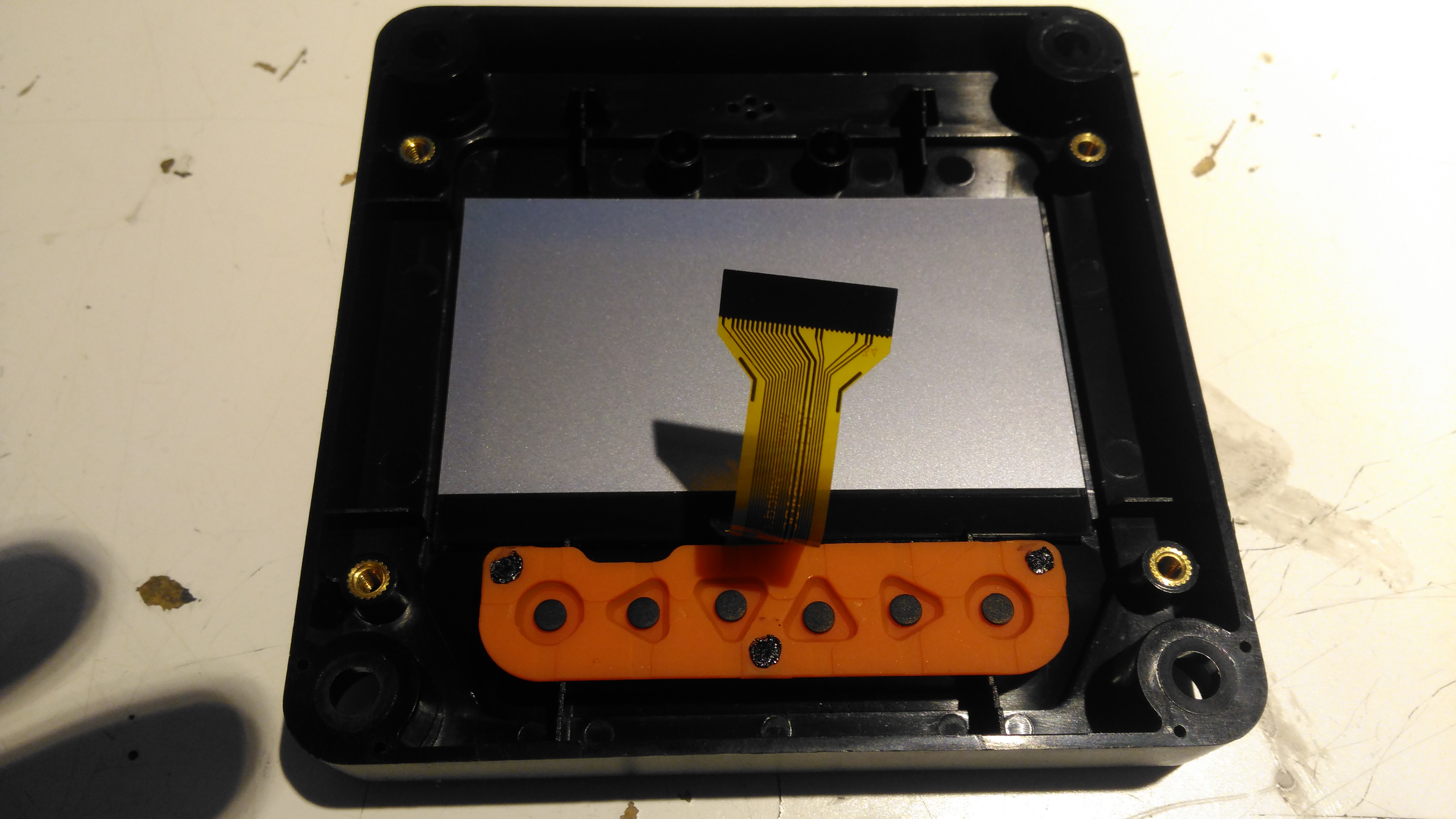
LCD Rear
The front case holds the LCD module in place with glue, and the rubber buttons are placed underneath, which is heat staked in place.
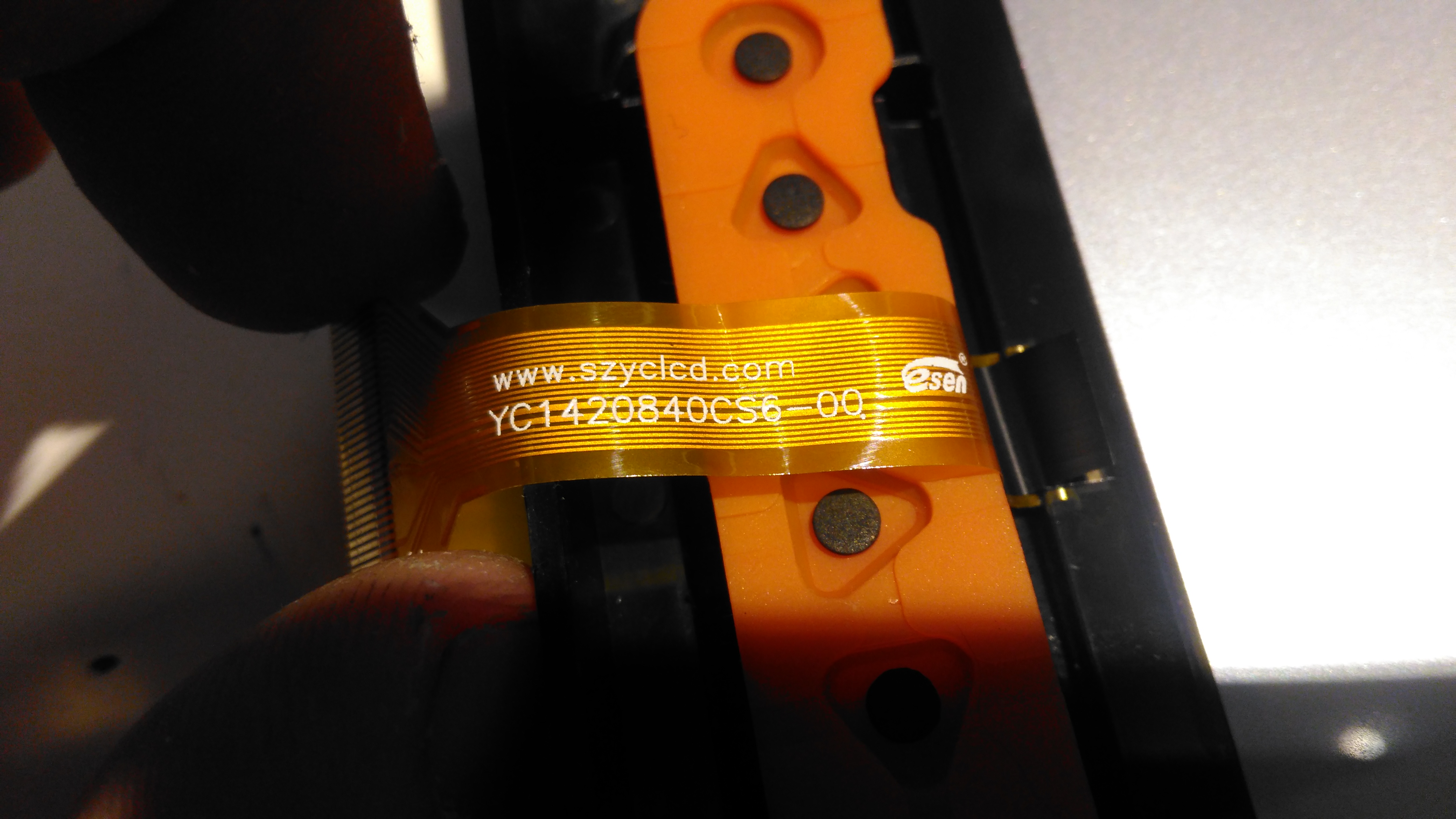
LCD Model
The LCD is a YC1420840CS6 from eCen in China. Couldn’t find much out about this specific LCD.
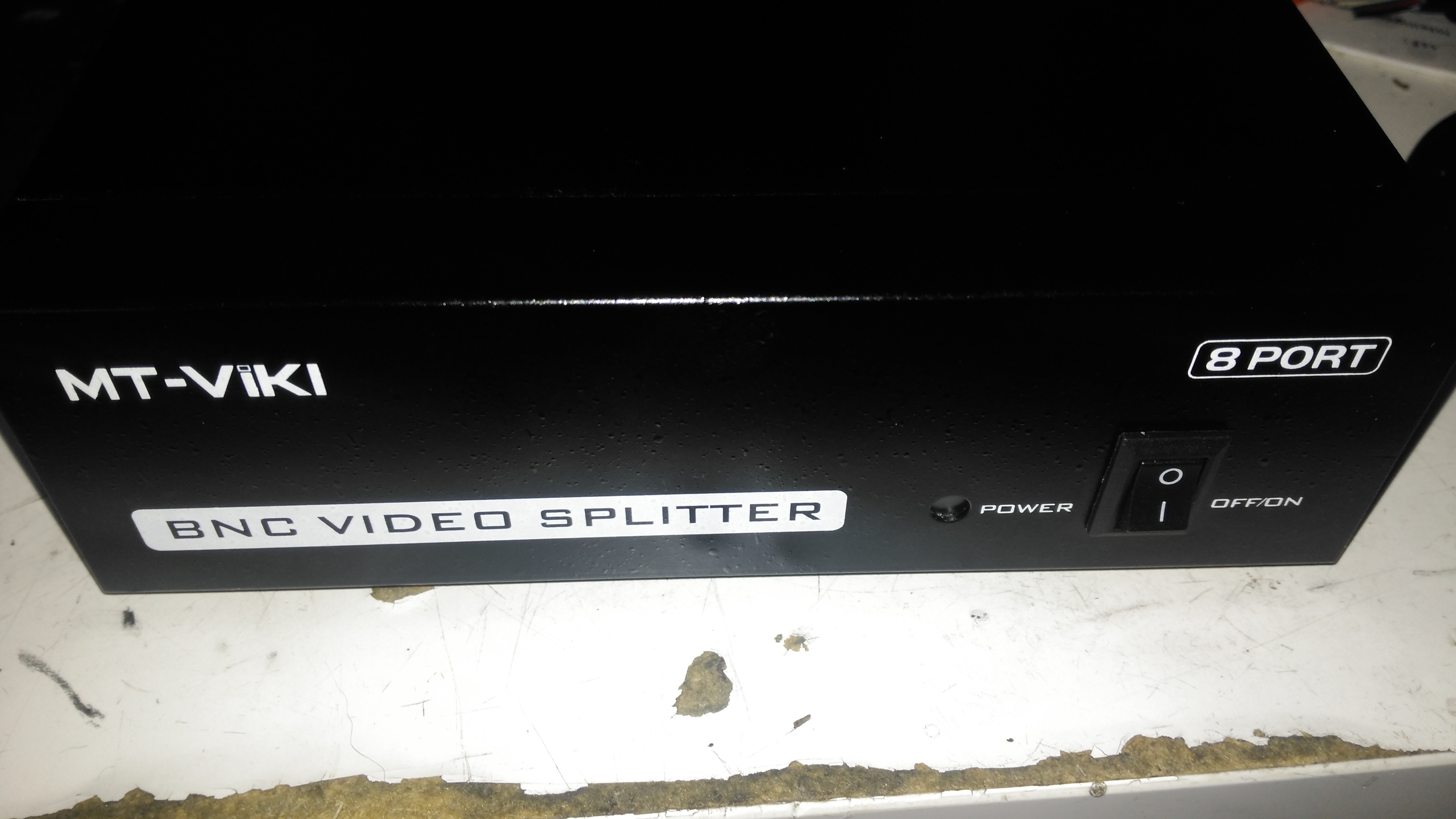
Time for another eBay special: this time it’s an 8-port video distribution amplifier, with BNC connections designed for commercial/industrial equipment. Not much on the front panel above, apart from the power switch & LED.
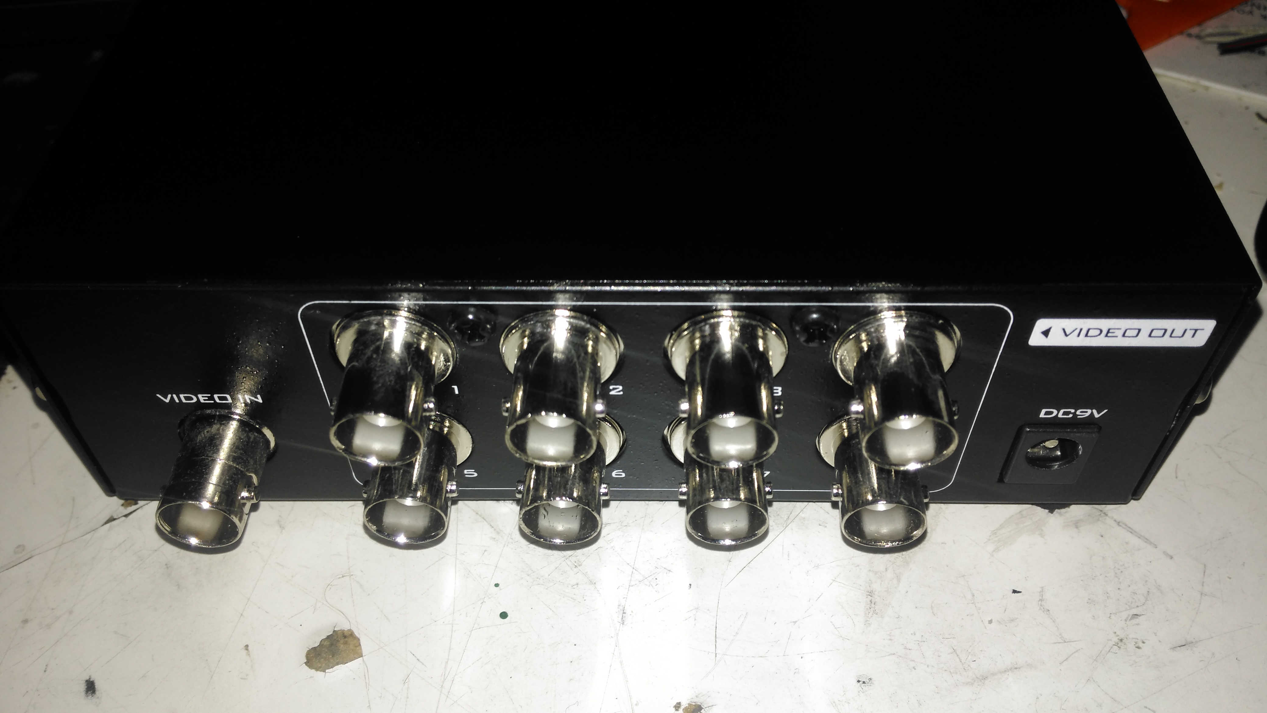
Rear Panel
The rear panel has all the connectors, input is on the left, while the outputs are in the centre. Power is supplied through the barrel jack on the right, 9v DC in this case.
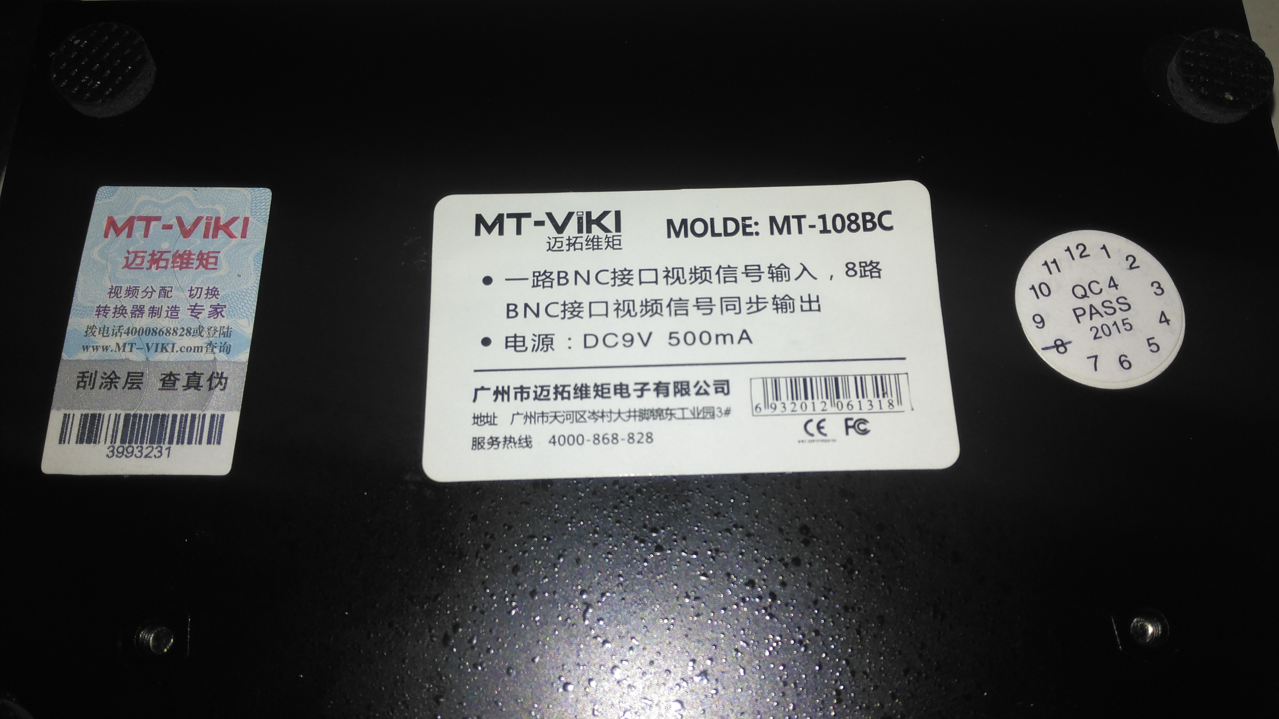
Data Label
Not much in English on the data labels, there’s also an authenticity label on the left to make sure you don’t get a fake.
Amplifier Board
Taking the lid off reveals a very small PCB, taking up less than a third of the aluminium case! The input stage is on the right, composed of a pair of SOT-23 transistors to buffer the incoming signal. There’s an KST812M6 PNP & an S9014 NPN Epitaxial. The signal is then fed to the output stages, all individual S9014 NPN transistors to the output ports.
The power LED is just poking in the general direction of the hole in the front panel, so this isn’t likely to work very well – it’s going to illuminate the inside of the case more!
Since I’ve discovered some nice high power PSUs in the form of Playstation 3 PSUs, it’s time to get a new Bench PSU Build underway!
Specifications
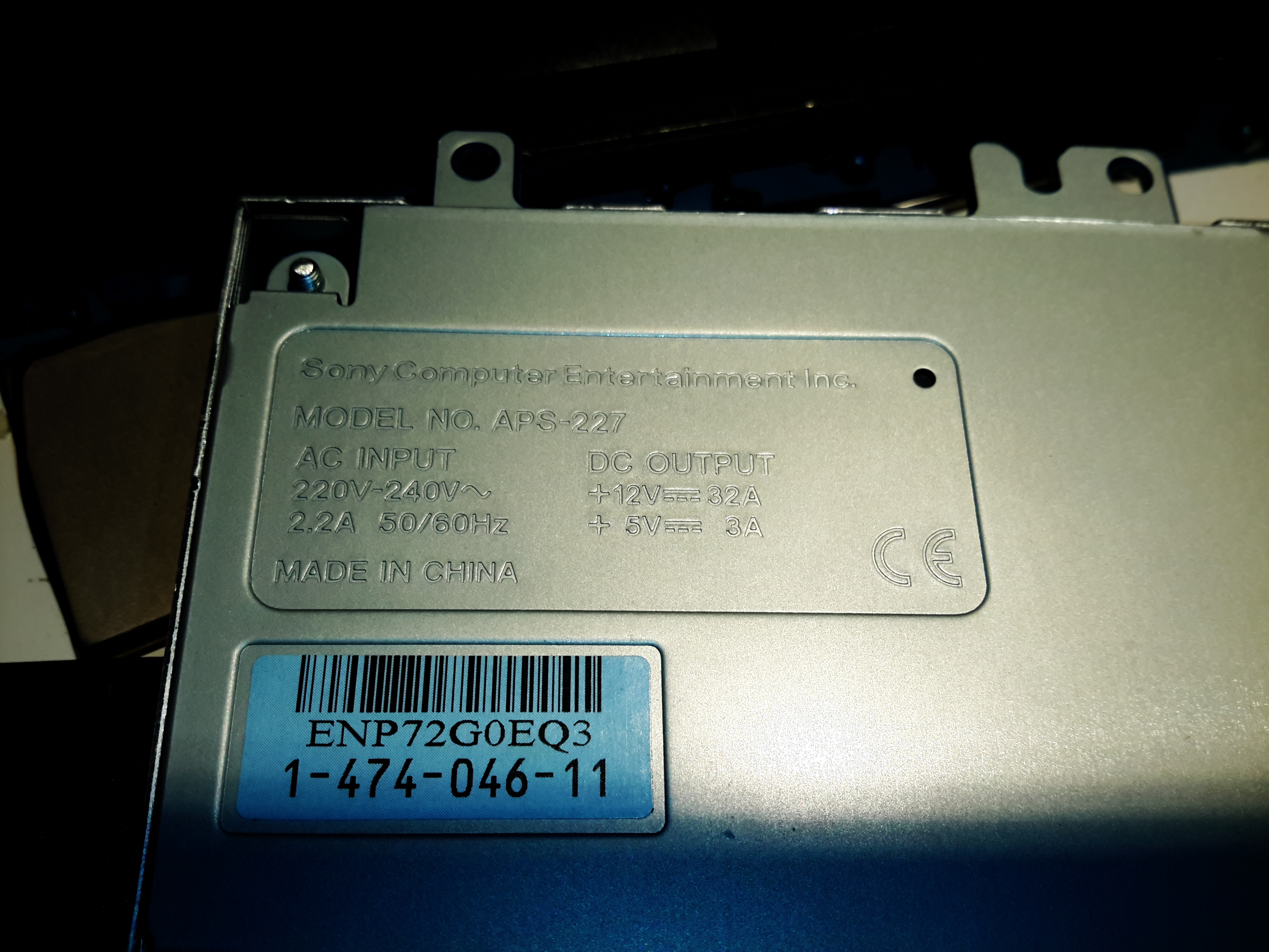
I’ve gone for the APS-227 version as it’s got the 32A rail. This makes things slightly beefier overall, as the loading will never be anywhere close to 100% for long, more headroom on the specs is the result.
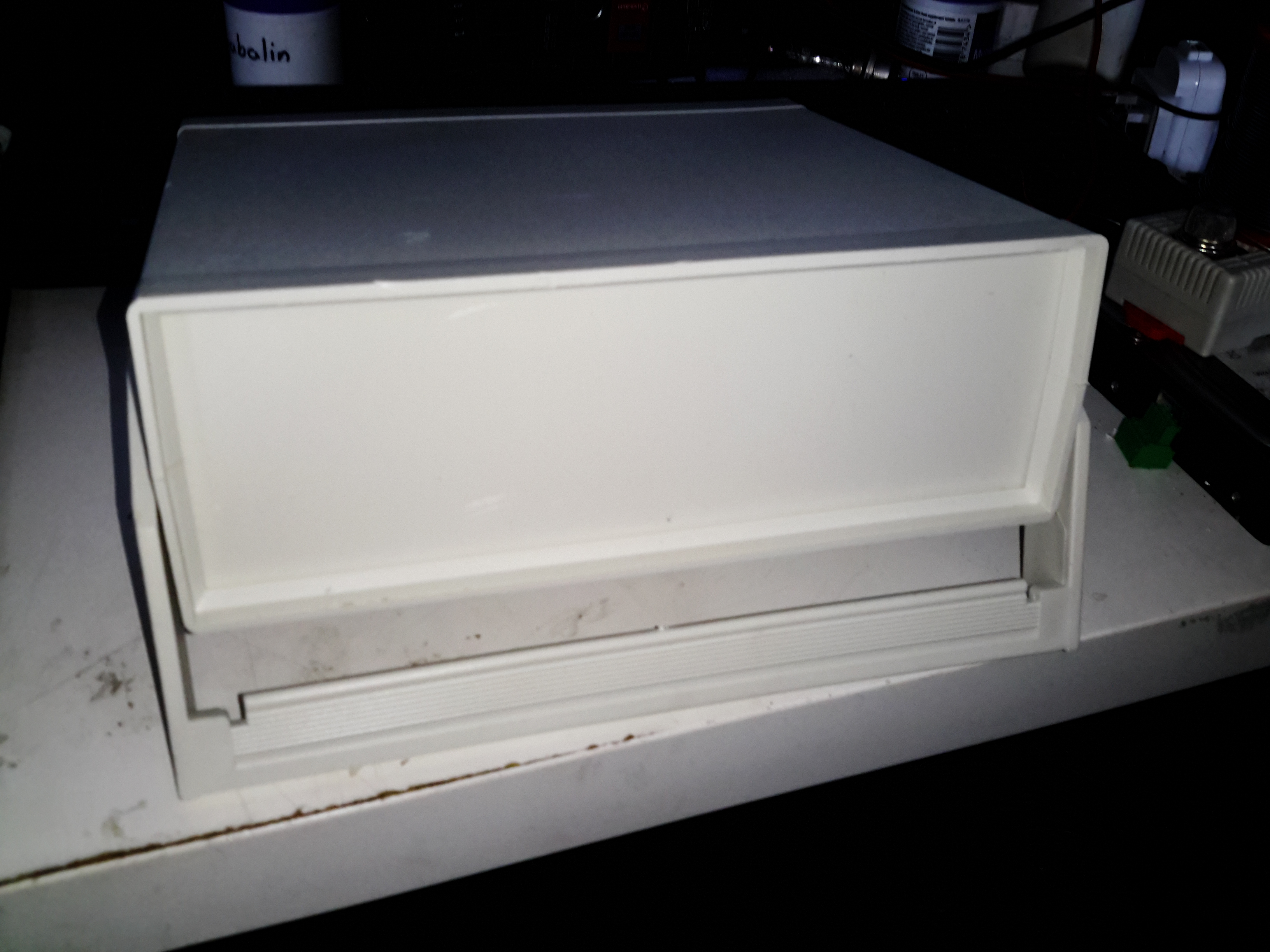
Desktop Instrument Case
The case I’ve chosen for this is an ABS desktop instrument case from eBay, the TE554 200x175x70mm. The ABS is easy to cut the holes for all the through-panel gear, along with being sturdy enough. Aluminium front & back panels would be a nice addition for a better look.
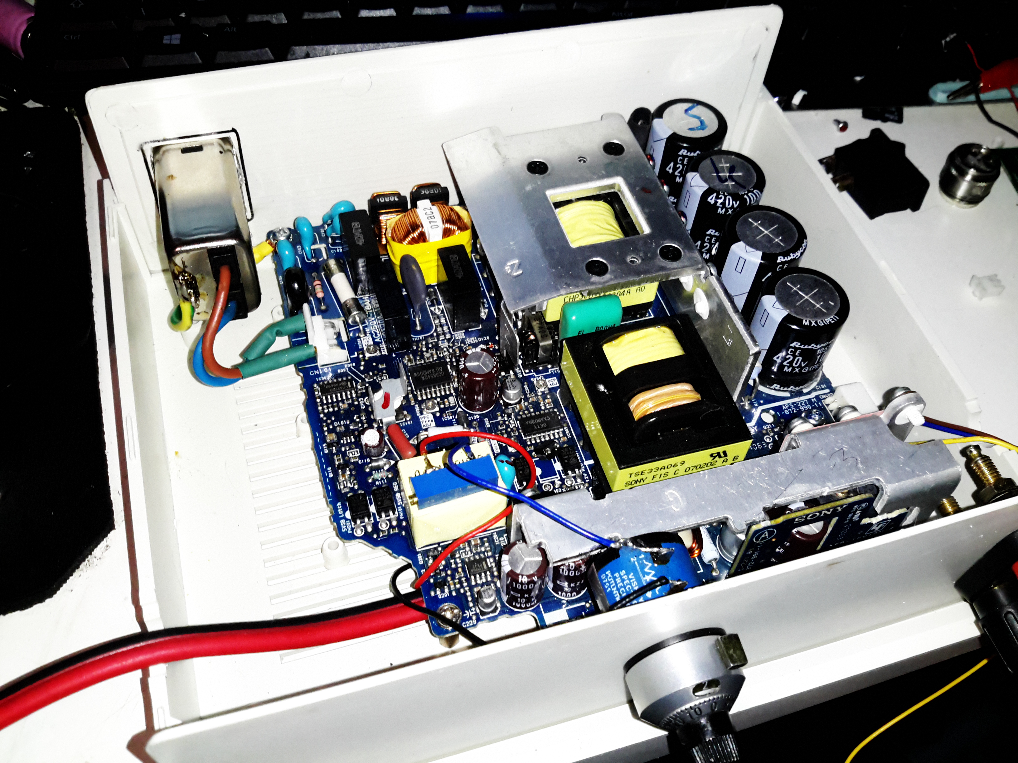
PSU Mounted
The PSU board is removed from it’s factory casing & installed on the bottom shell half, unfortunately the moulded-in posts didn’t match the screw hole locations so I had to mount some brass standoffs separately. The AC input is also fitted here, I’ve used a common-mode filter to test things (this won’t be staying, as it fouls one of the case screw holes). The 40A rated DC output cable is soldered directly to the PCB traces, as there’s no room under the board to fit the factory DC power connector. (This is the biggest case I could find on eBay, and things are still a little tight). Some minor modifications were required to get the PCB to fit correctly.
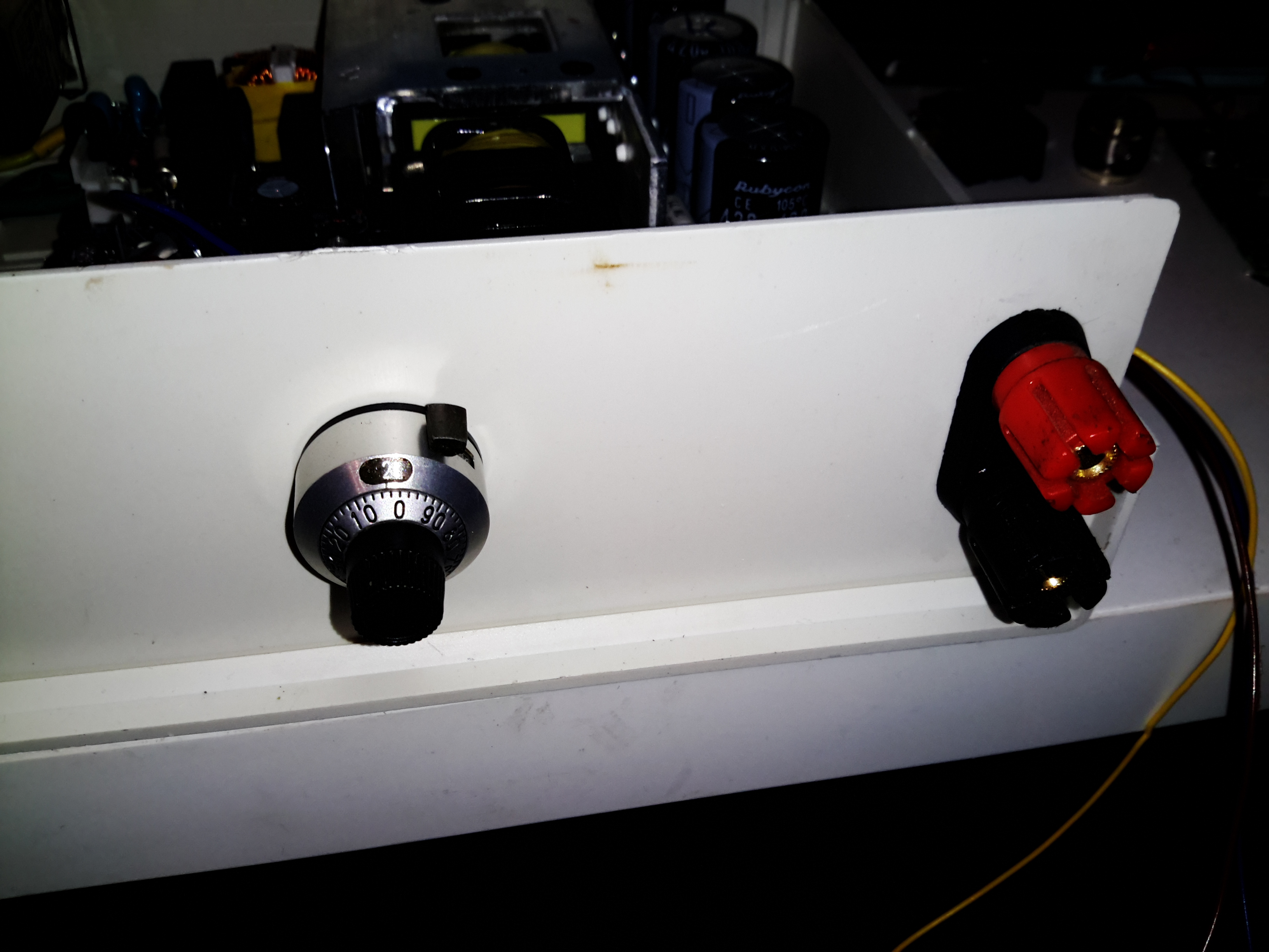
Output Terminals & Adjuster
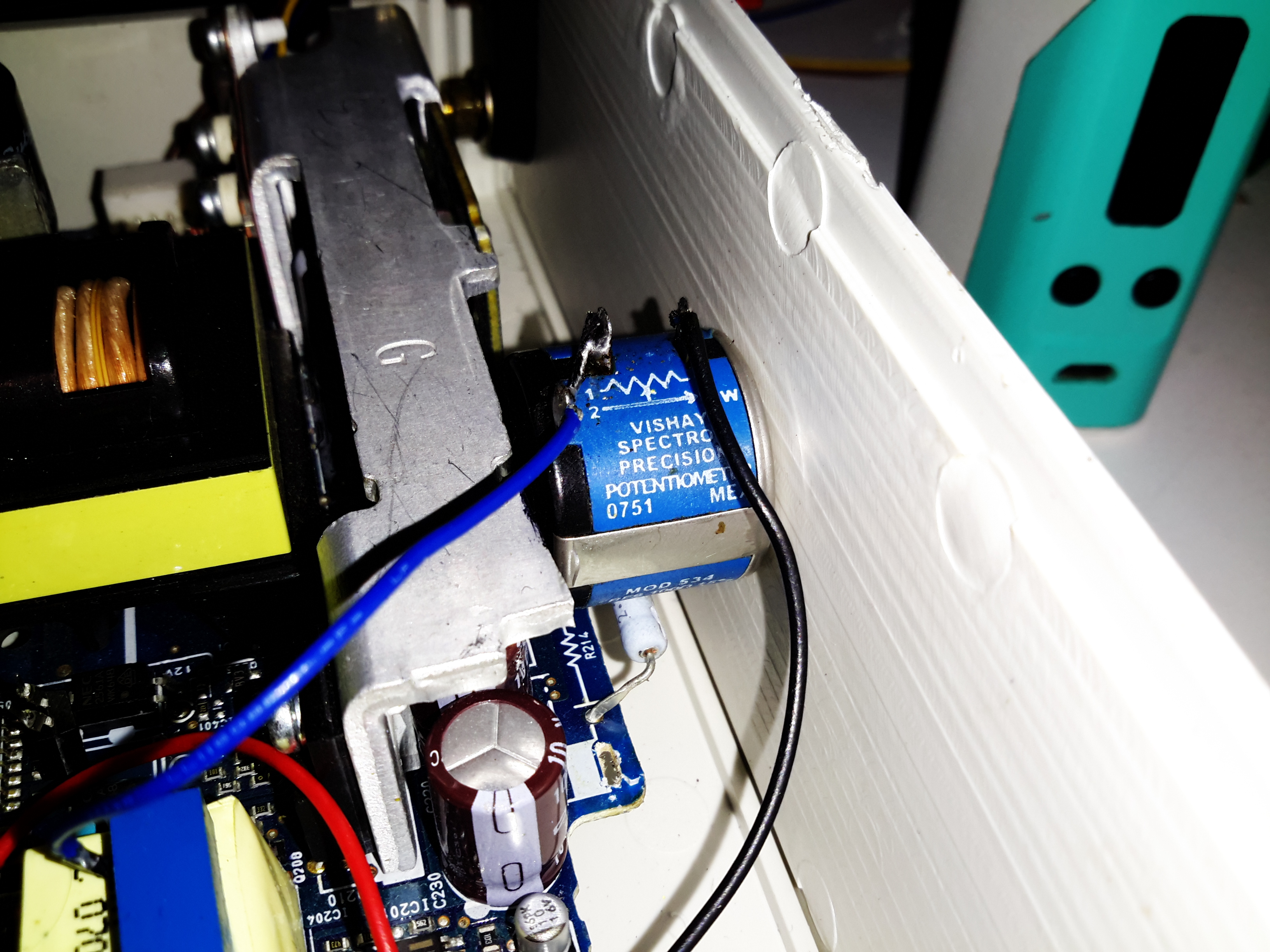
I decided to add some limited voltage adjustment capability to the front panel, I had a 100Ω Vishay Spectrol Precision 10-turn potentiometer in my parts bin, from a project long since gone that just about fits between the panel & the output rectifier heatsink. The trimpot I added when I first posted about these PSUs is now used to set the upper voltage limit of 15 volts. (The output electrolytics are 16v rated, and are in an awkward place to get at to change for higher voltage parts). The binding posts are rated to 30A, and were also left over from a previous project.
Vishay Spectrol 10-Turn
Addon Regulator Components
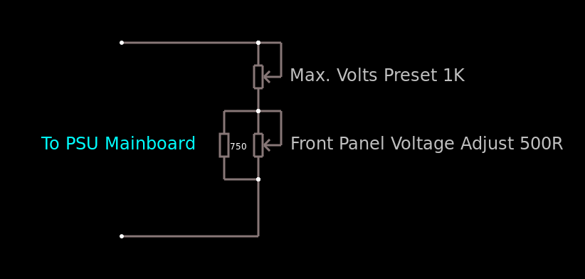
This front panel potentiometer is electrically in series with the trimpot glued to the top of the auxiliary transformer, see above for a simple schematic of the added components. In this PSU, reducing the total resistance in the regulator circuit increases the voltage, so make sure the potentiometer is wired correctly for this!
After some experimentation, a 500Ω 10-turn potentiometer would be a better match, with a 750Ω resistor in parallel to give a total resistance range on the front panel pot of 300Ω. This will give a lower minimum voltage limit of about 12.00v to make lead-acid battery charging easier.
I’ve had to make a minor modification to the output rectifier heatsink to get this pot to fit in the available space, but nothing big enough to stop the heatsink working correctly.
Terminal Posts
Here I’ve got the binding posts mounted, however the studs are a little too long. Once the wiring is installed these will be trimmed back to clear both the case screw path & the heatsink. (The heatsink isn’t a part of the power path anyway, so it’s isolated).
Power Meter Control Board & Fan
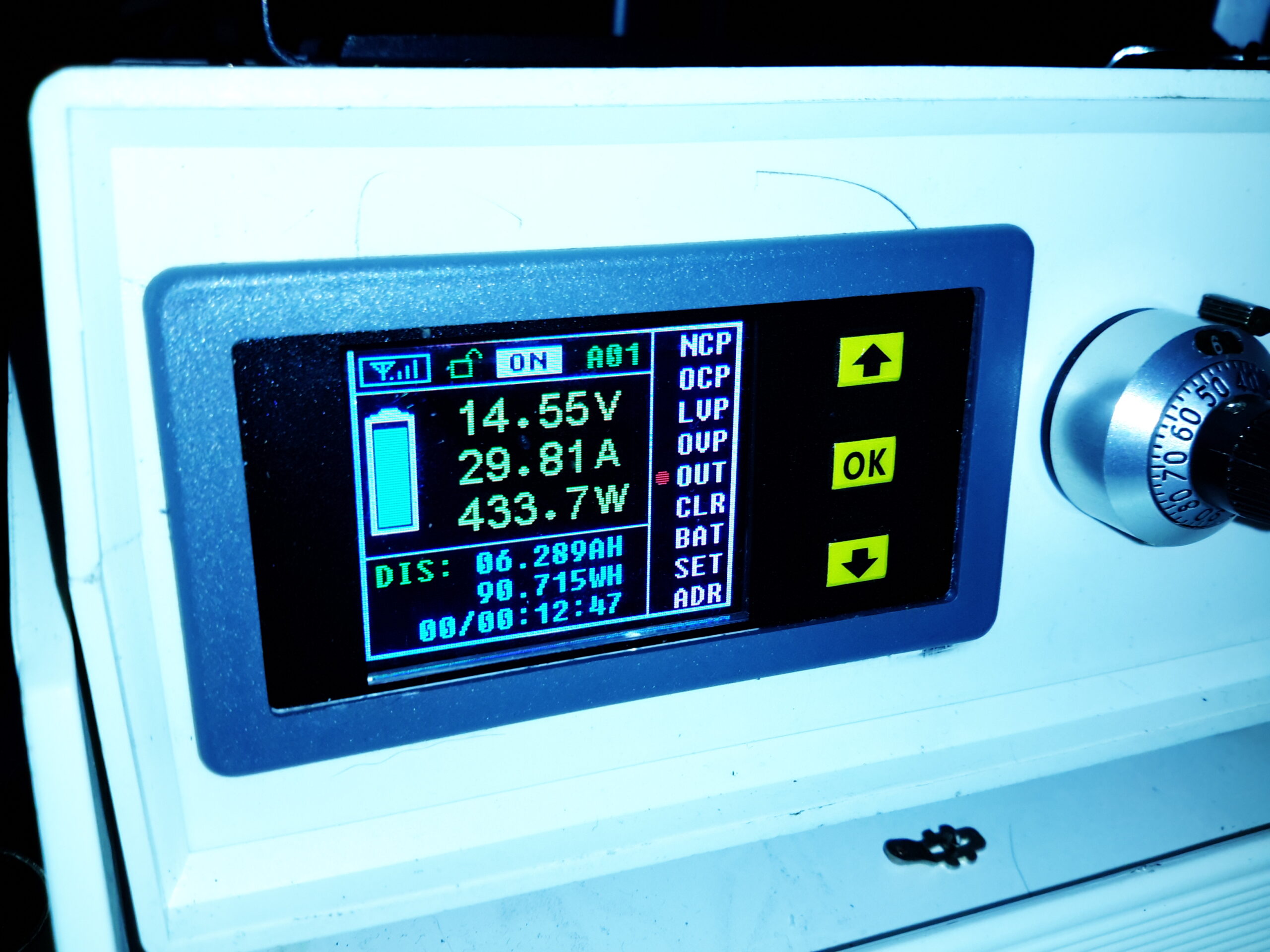
To keep the output rectifier MOSFETs cool, there’s a fan mounted in the upper shell just above their location, this case has vents in the bottom already moulded in for the air to exit. The fan is operated with the DC output contactor, only running when the main DC is switched on. This keeps the noise to a minimum when the supply doesn’t require cooling. The panel meter control board is also mounted up here, in the only empty space available. The panel meter module itself is a VAC-1030A from MingHe.
Meter Power Board
The measurement shunt & main power contactor for the DC output is on another board, here mounted on the left side of the case. The measurement shunt is a low-cost one in this module, I doubt it’s made of the usual materials of Manganin or Constantan, this is confirmed by my meansurements as when the shunt heats up from high-power use, the readings drift by about 100mA. The original terminal blocks this module arrived with have been removed & the DC cables soldered directly to the PCB, to keep the number of high-current junctions to a minimum. This should ensure the lowest possible losses from resistive heating.
Meter Panel Module
The panel meter module iself is powered from the 5v standby rail of the Sony PSU, instead of the 12v rail. This allows me to keep the meter on while the main 12v output is switched off.
PSU Internals
here’s the supply with everything fitted to the lower shell – it’s a tight fit! A standard IEC connector has been fitted into the back panel for the mains input, giving much more clearance for the AC side of things.
Inside View
With the top shell in place, a look through the panel cutout for the meter LCD shows the rather tight fit of all the meter components. There’s about 25mm of clearance above the top of the PSU board, giving plenty of room for the 40mm cooling fan to circulate air around.
Load Test
Here’s the finished supply under a full load test – it’s charging a 200Ah deep cycle battery. The meter offers many protection modes, so I’ve set the current limit at 30A – preventing Sony’s built in over current protection on the PSU tripping with this function is a bonus, as the supply takes a good 90 seconds to recover afterwards. I’ll go into the many modes & features of this meter in another post.
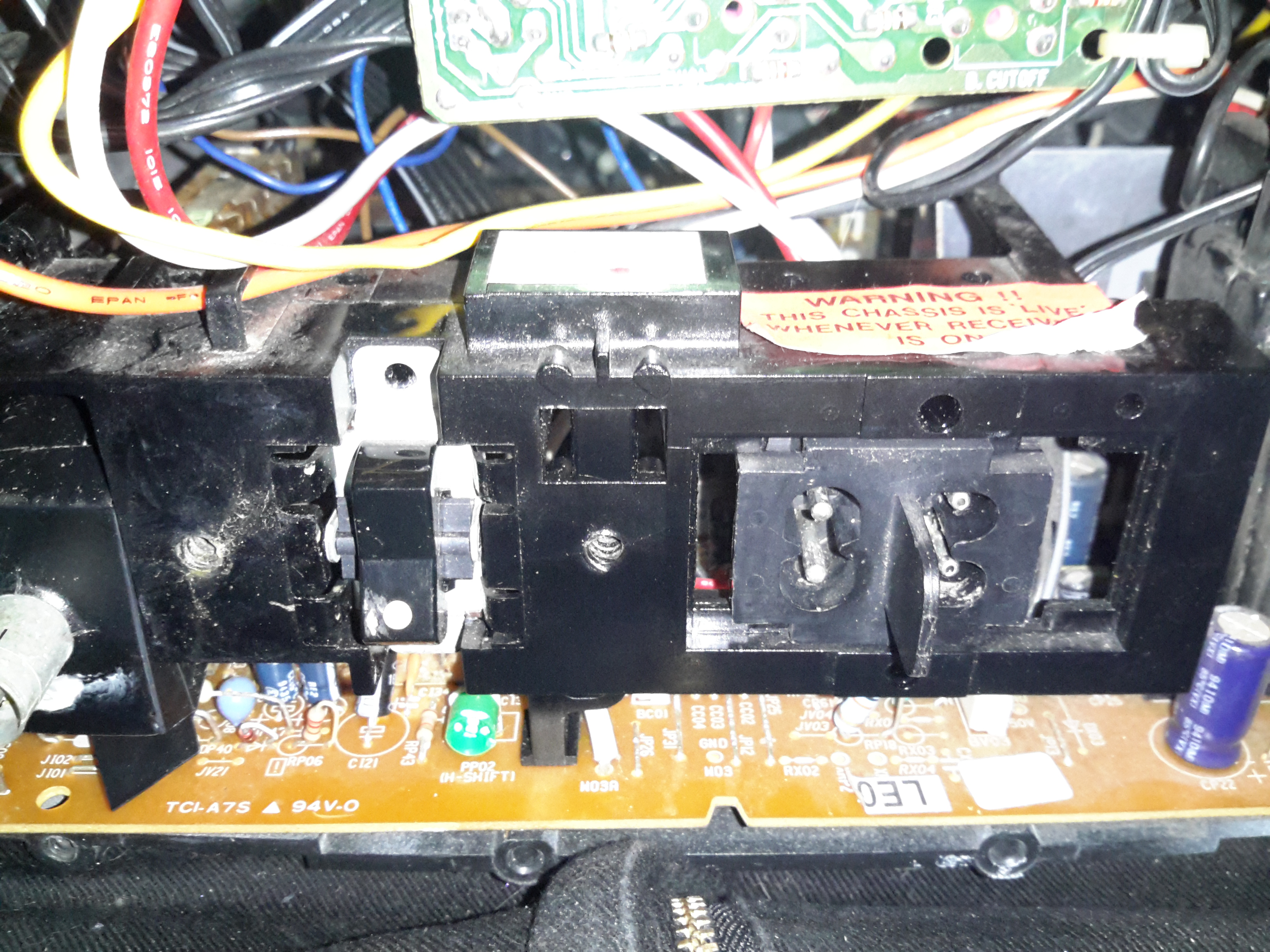
Here’s the other TV that was picked up from the local water point having been put of to be recycled. This one is much newer than the Thorn TV, a 10″ colour version from Ferguson.
RCA 27GDC85X CRT
The colour CRT used is an RCA branded one, 27GDC85X.
Power Inputs
Like the other TV, this one is dual voltage input, mains 240v & 12v battery. This TV is a factory conversion of a standard 240v AC chassis though.
HV PSU
The 12v power first goes into this board, which looked suspiciously like an inverter. Measuring on the output pins confirmed I was right, this addon board generates a 330v DC supply under a load, but it’s not regulated at all, under no load the output voltage shoots up to nearly 600v!
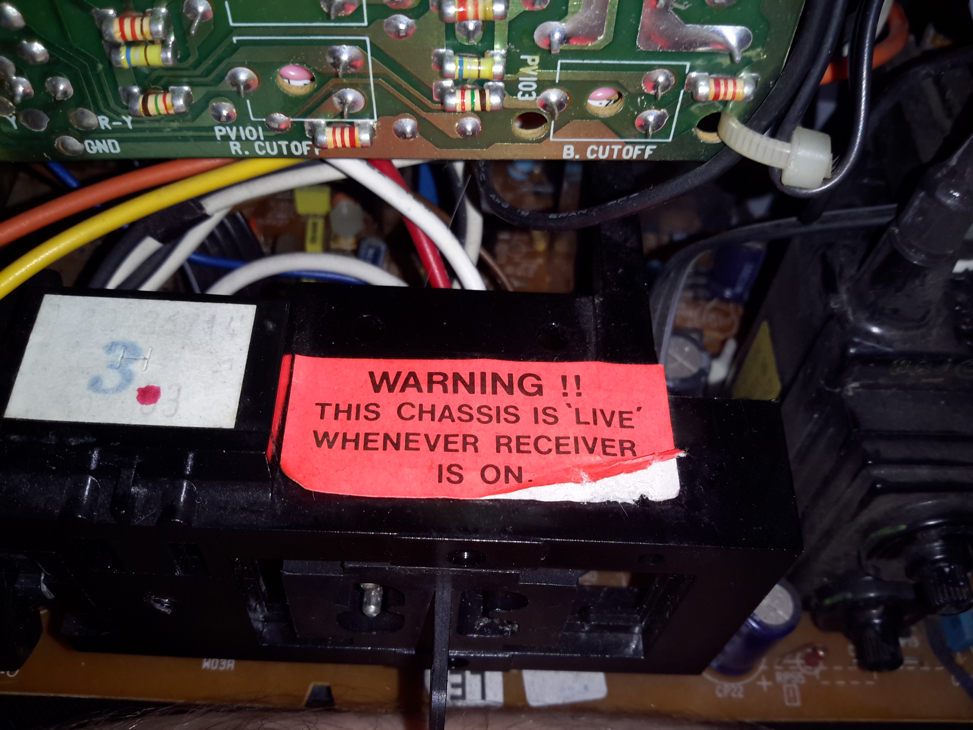
Live Chassis
I’ve not seen one of these labels on a TV for many years, when back in the very old TV sets the steel chassis would be used to supply power to parts of the circuitry, to save on copper. Although it doesn’t have a metal chassis to actually become live, so I’m not sure why it’s here.
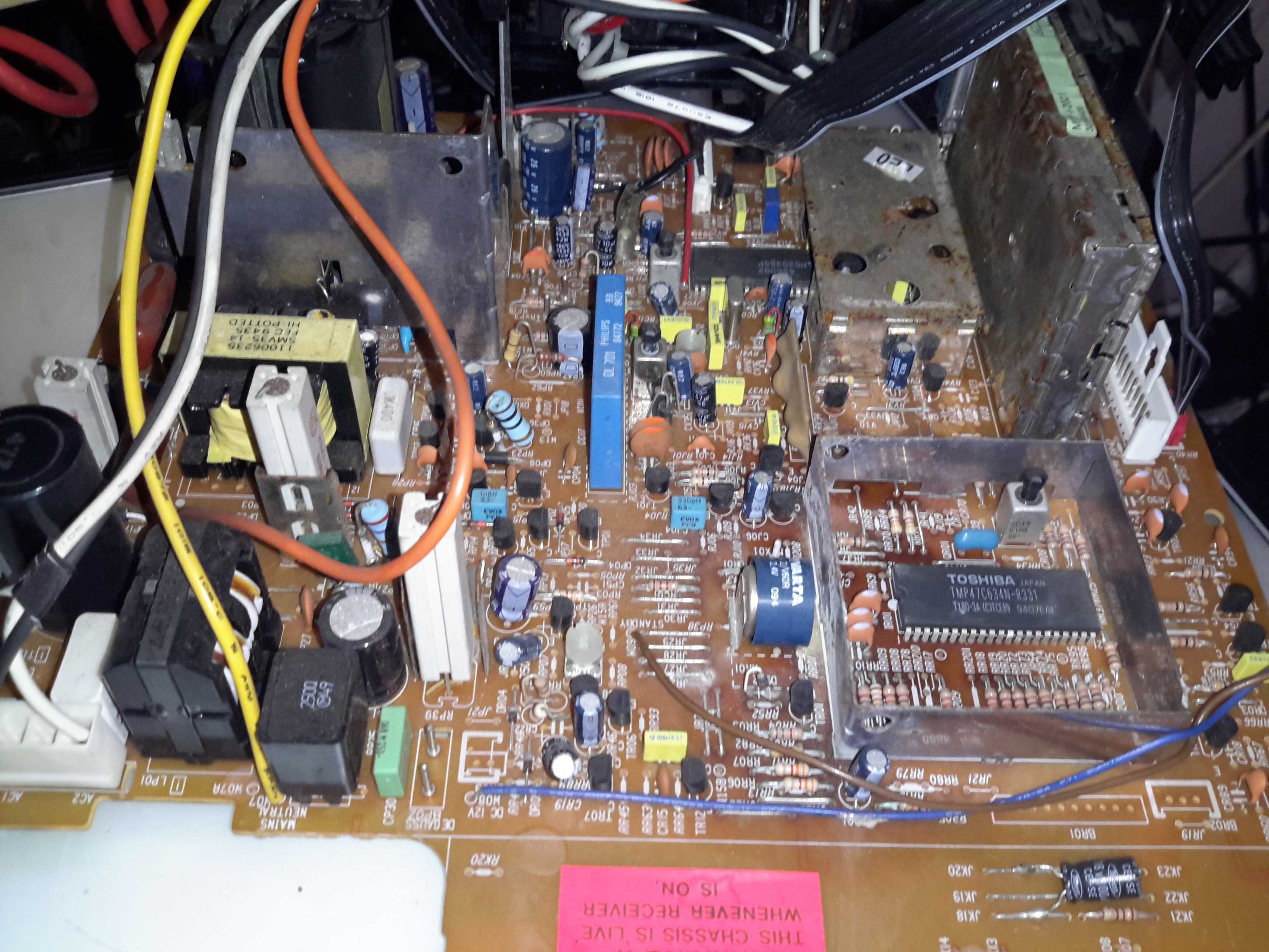
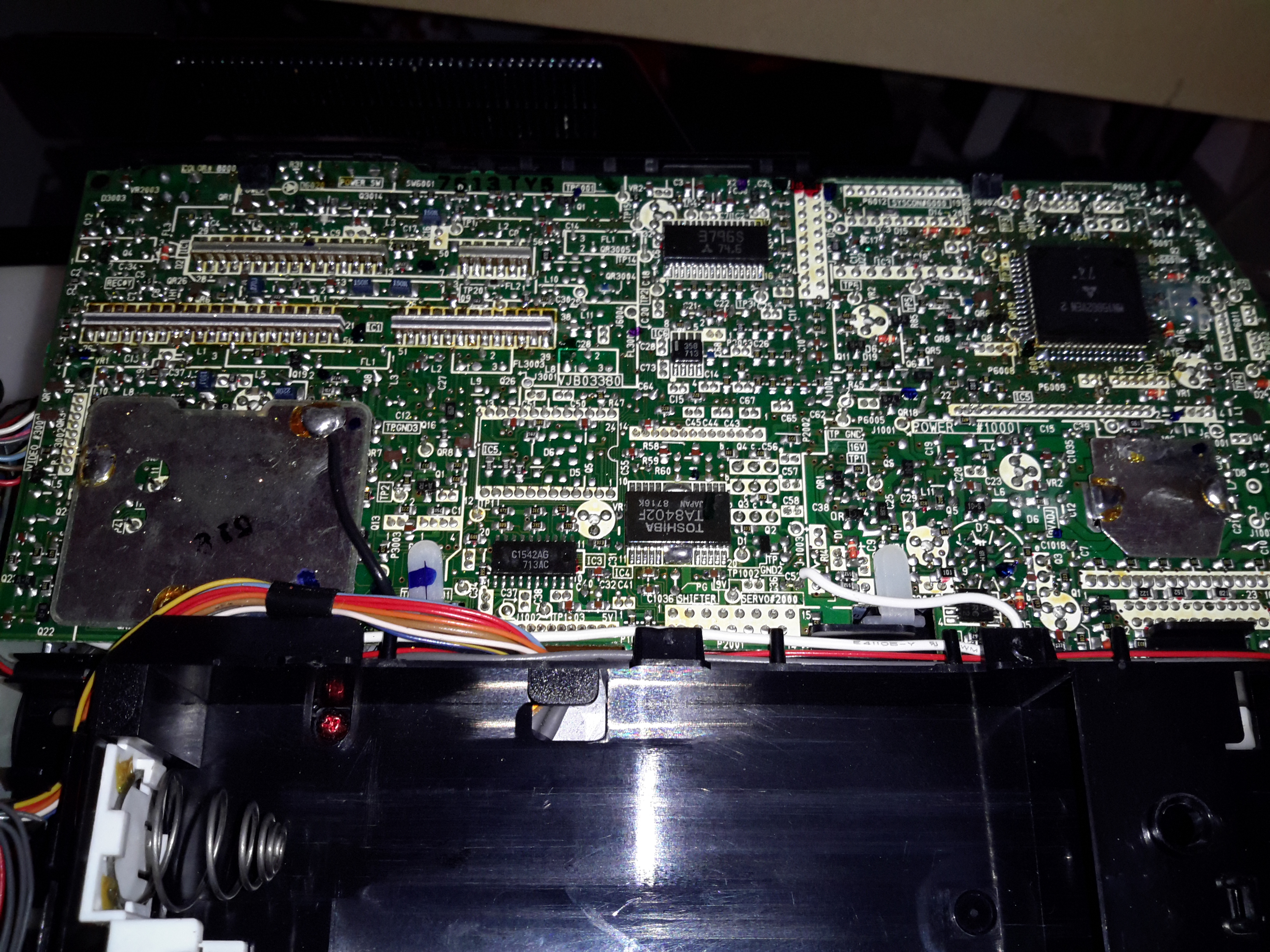
Main PCB
The main PCB is much more integrated in this newer TV, from the mid 90’s, everything is pretty much taken care of by silicon by this point.
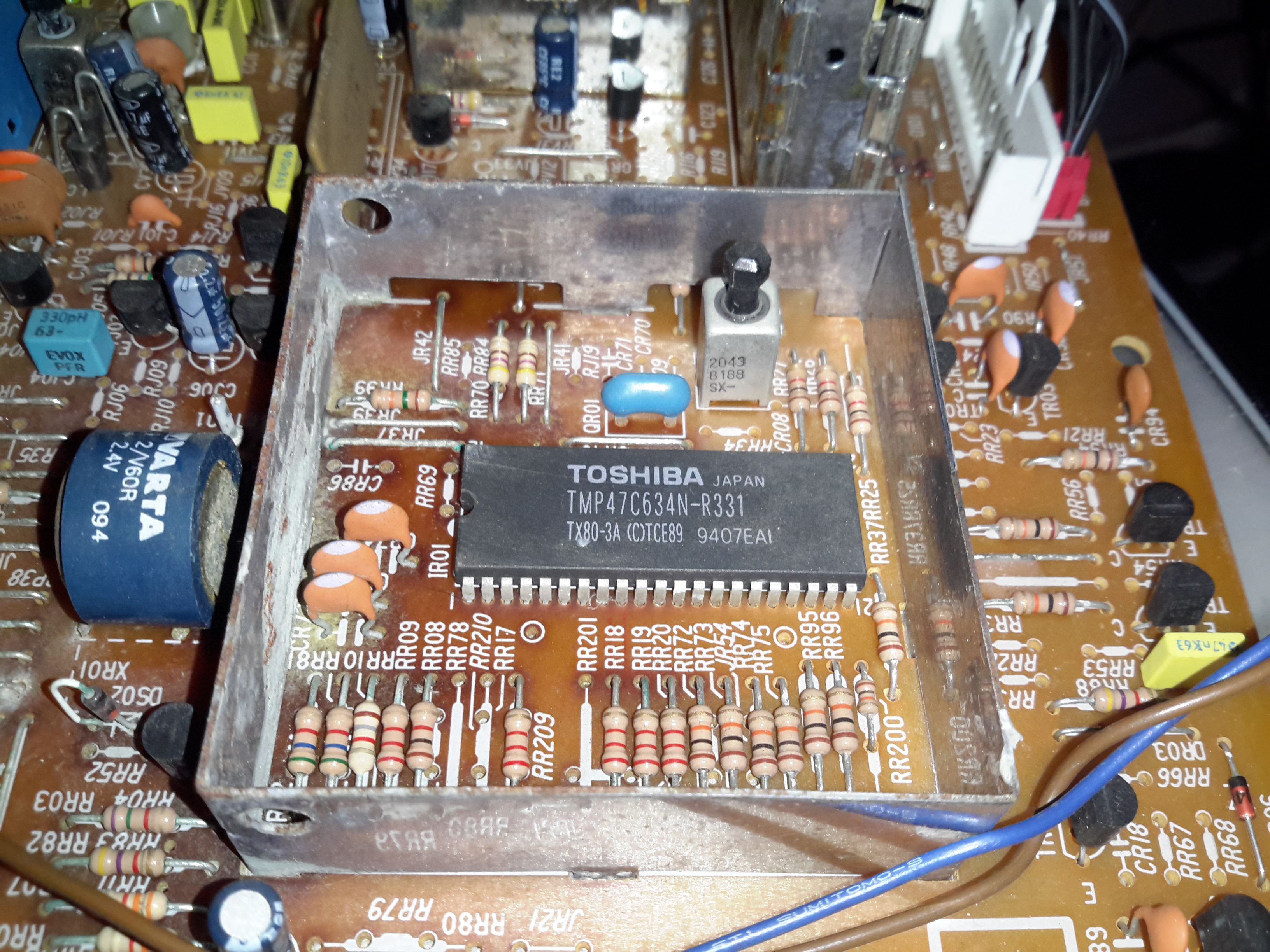
Main Microcontroller
This Toshiba µC takes care of channel switching & displaying information on the CRT. The tuner in this TV is electronically controlled.
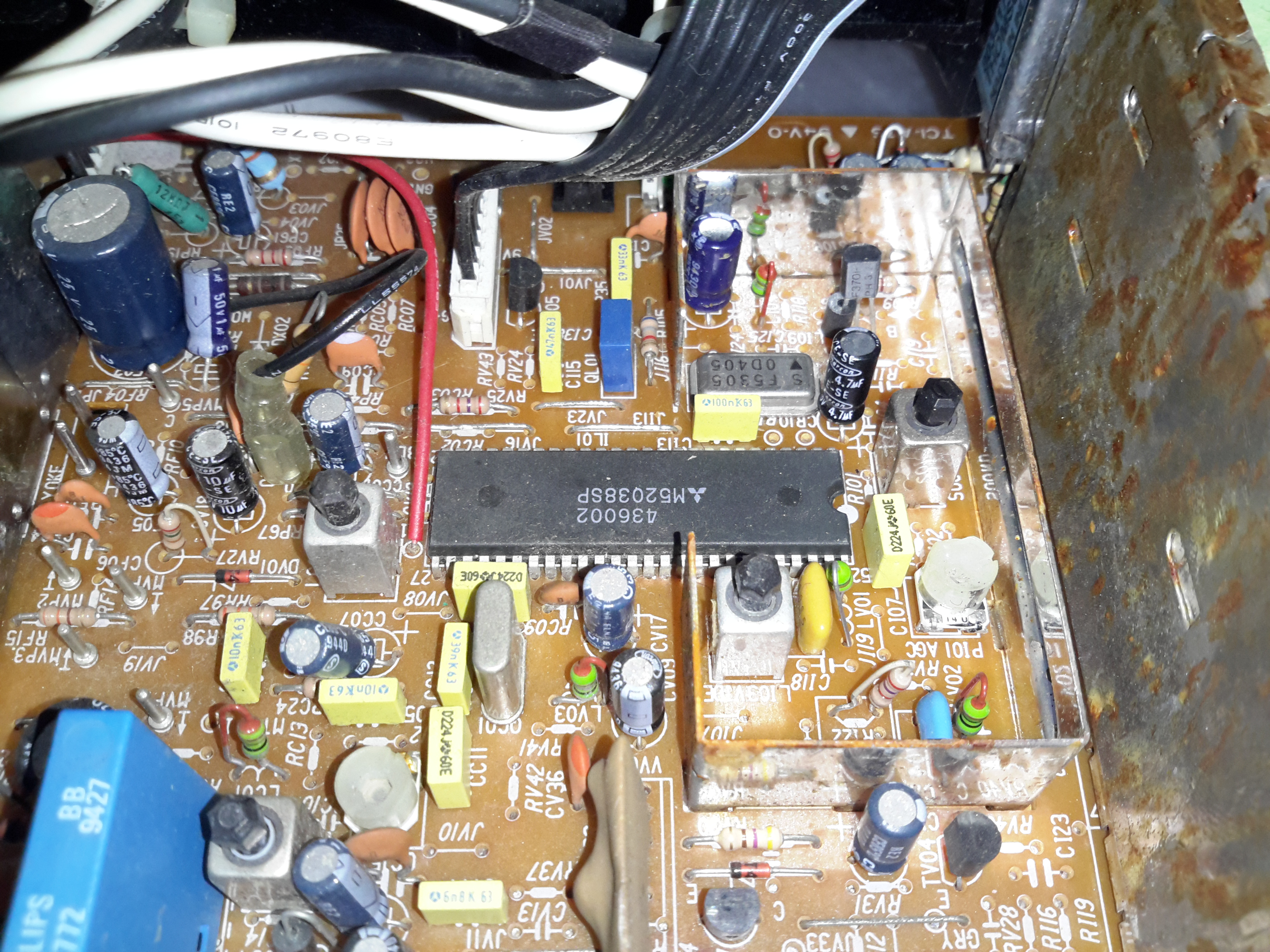
PAL Signal Processor
The video signal is handled by this Mitsubishi IC, which is a PAL Signal Processor, this does Video IF, Audio IF, Chroma, & generates the deflection oscillators & waveforms to drive the yoke.
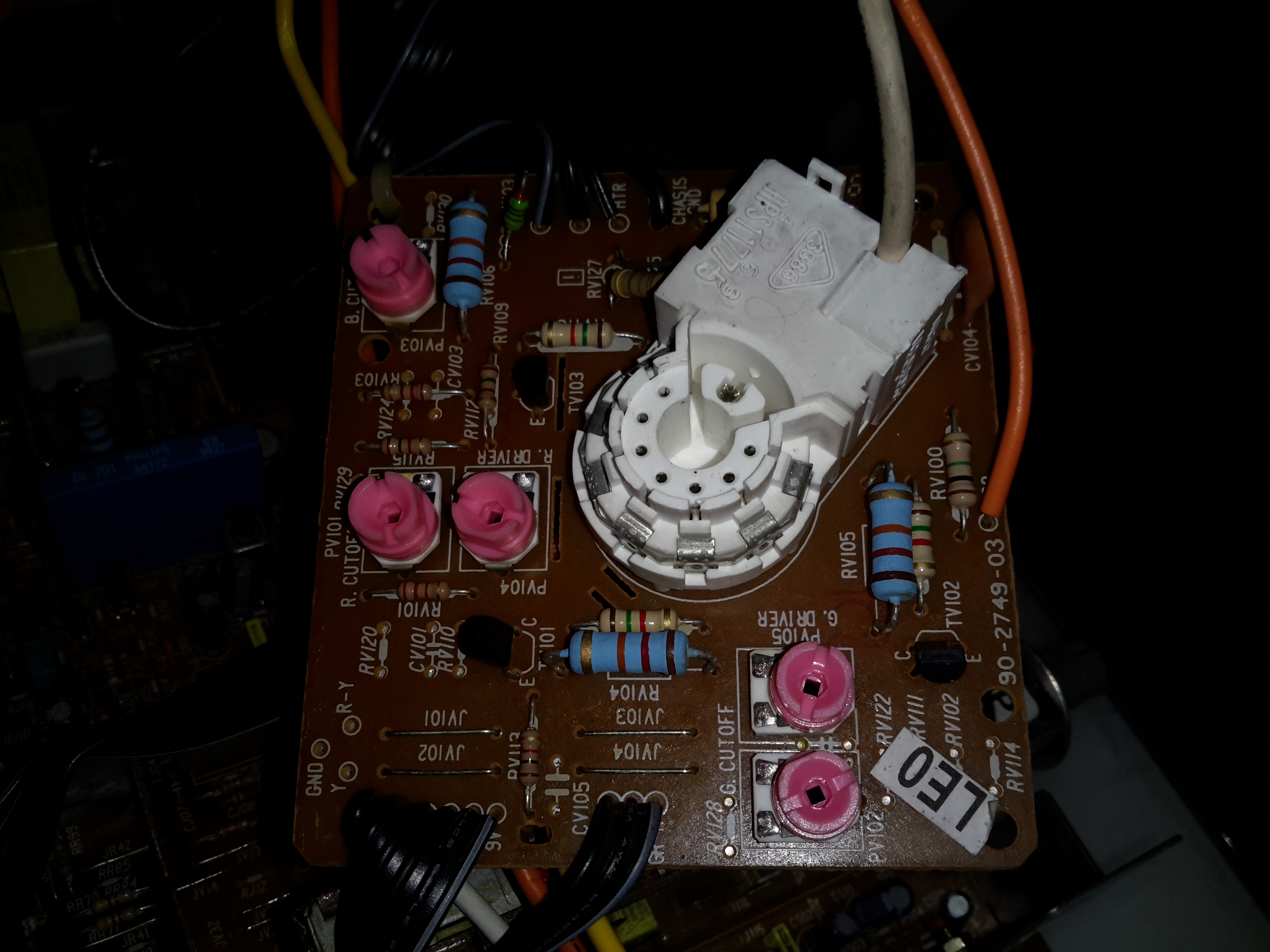
CRT Adjustments
There are some adjustments on the CRT neck board for RGB drive levels & cutoff levels. This board also had the final video amplifiers onboard, which drive the CRT cathodes.
Here’s a useful tool for testing both power supplies & batteries, a dummy load. This unit is rated up to 60W, at voltages from 1v to 25v, current from 200mA to 9.99A.
This device requires a 12v DC power source separate from the load itself, to power the logic circuitry.
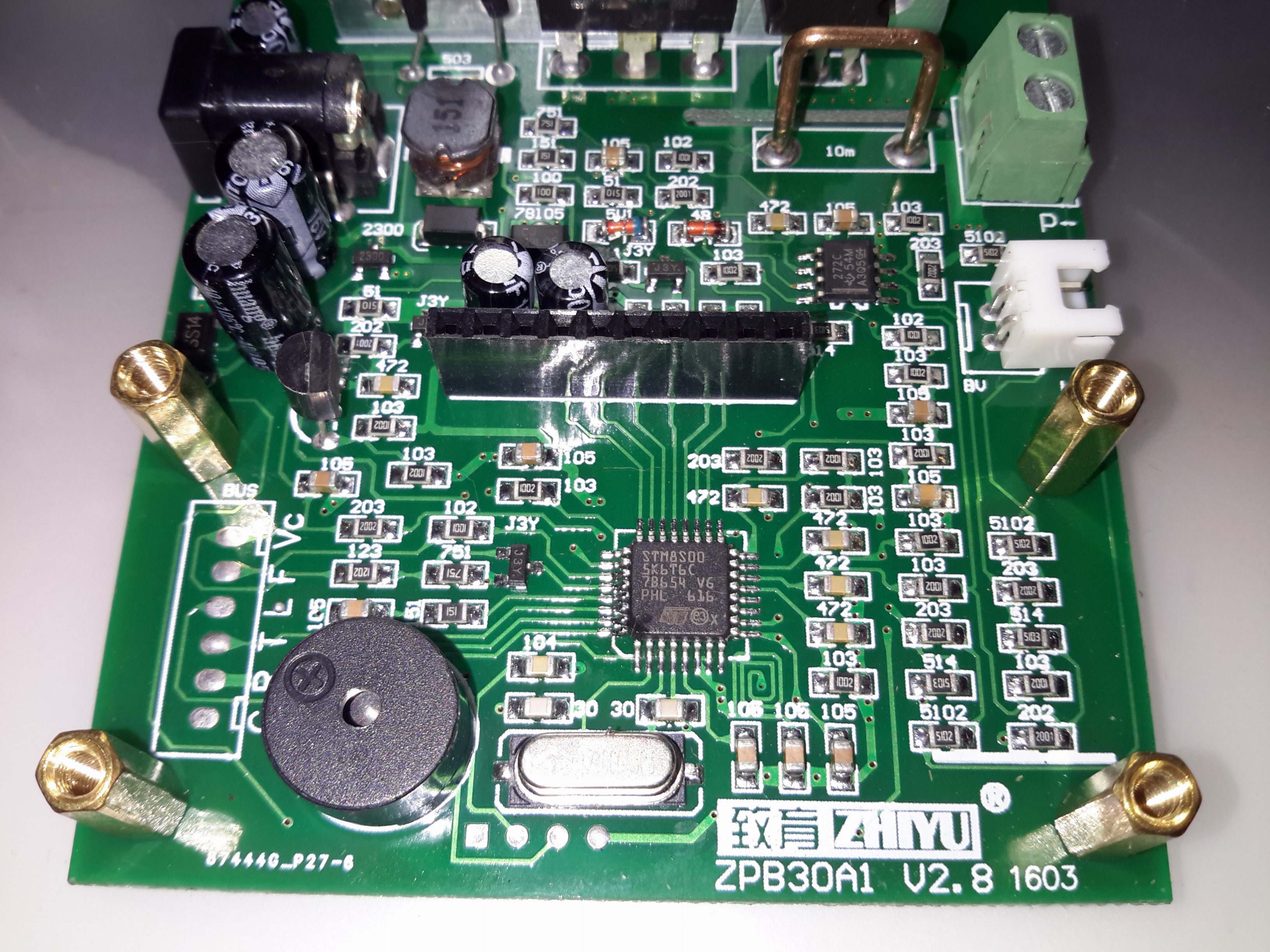
Microcontroller Section
Like many of these modules, the brains of the operation is an STM8 microcontroller. There’s a header to the left with some communication pins, the T pin transmits the voltage when the unit is operating, along with the status via RS232 115200 8N1. This serial signal is only present in DC load mode, the pin is pulled low in battery test mode. The 4 pins underneath the clock crystal are the programming pins for the STM8.
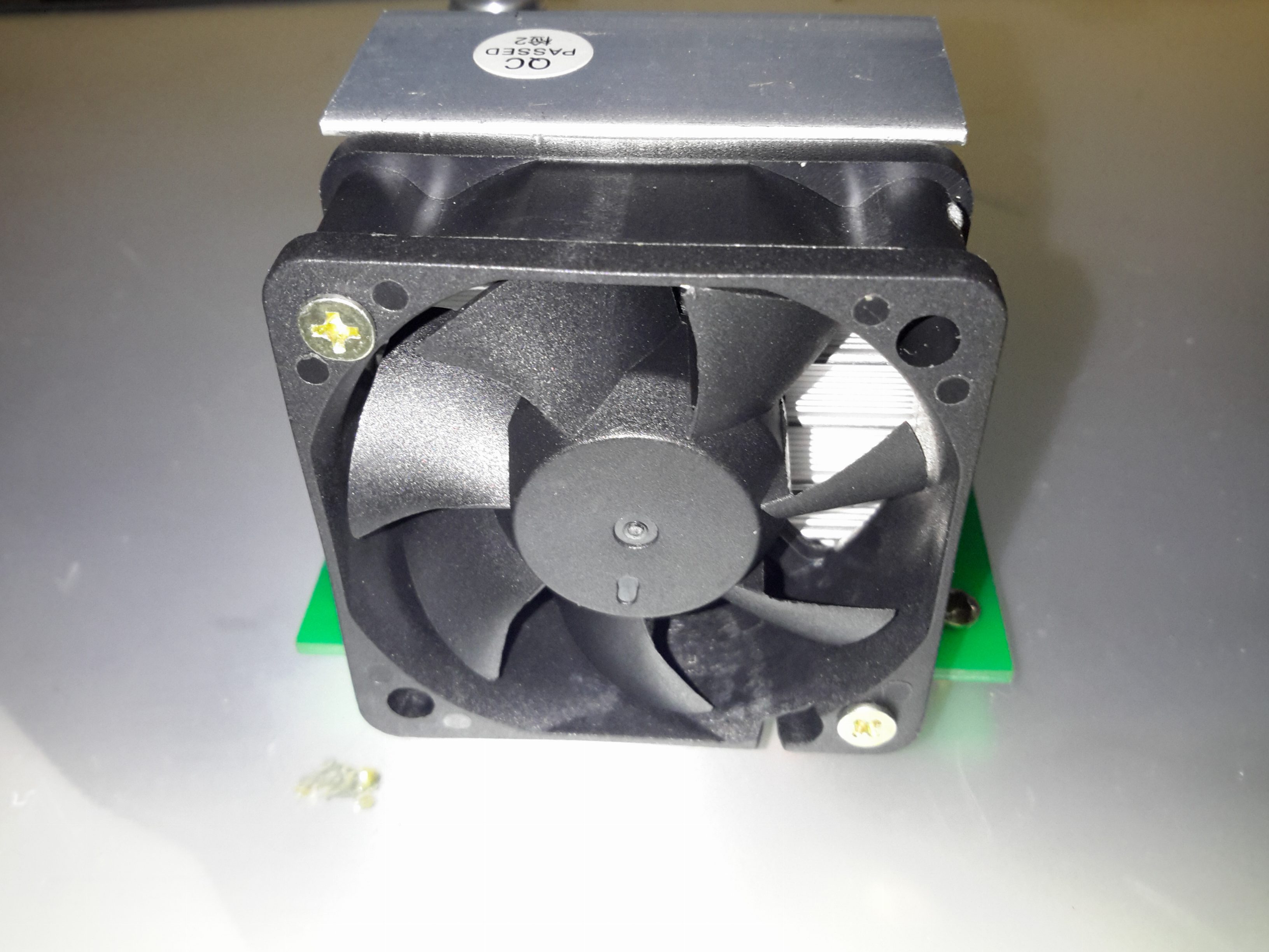
Serial CommsCooling Fan
The main heatsink is fan cooled, the speed is PWM controlled via the microcontroller depending on the temperature.
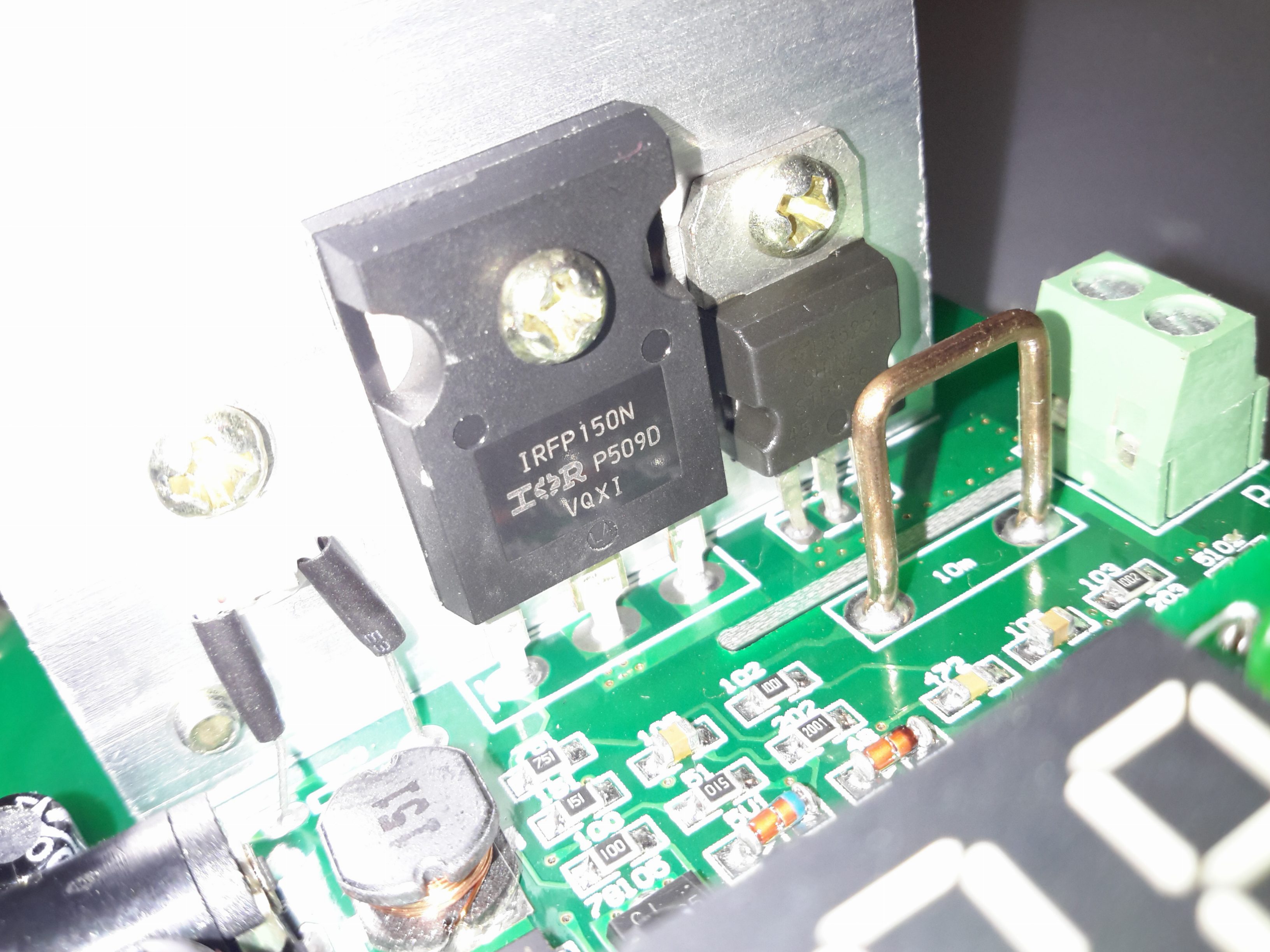
Main MOSFET
The main load MOSFET is an IRFP150N from Infineon. This device is rated at 100v 42A, with a max power dissipation of 160W. On the right is a dual diode for reverse polarity protection, this is in series with the MOSFET. On the left is the thermistor for controlling fan speed.
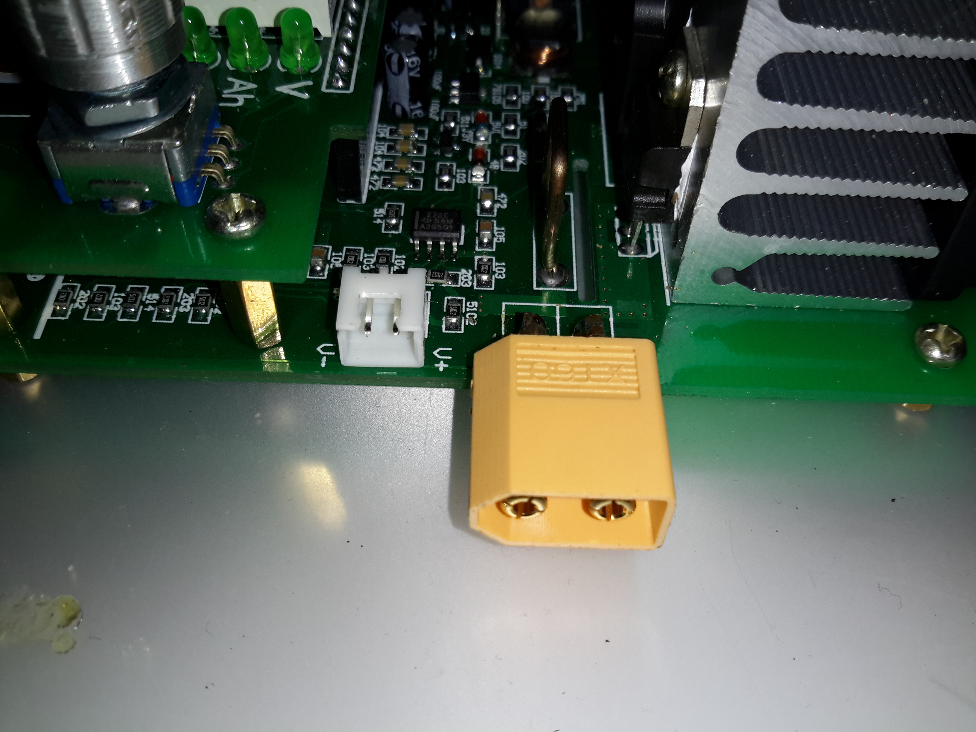
Load Terminals
The load is usually connected via a rising clamp terminal block. I’ve replaced it with a XT60 connector in this case as all my battery holders are fitted with these. This also removes the contact resistance of more connections for an adaptor cable. The small JST XH2 connector on the left is for remote voltage sensing. This is used for 4-wire measurements.
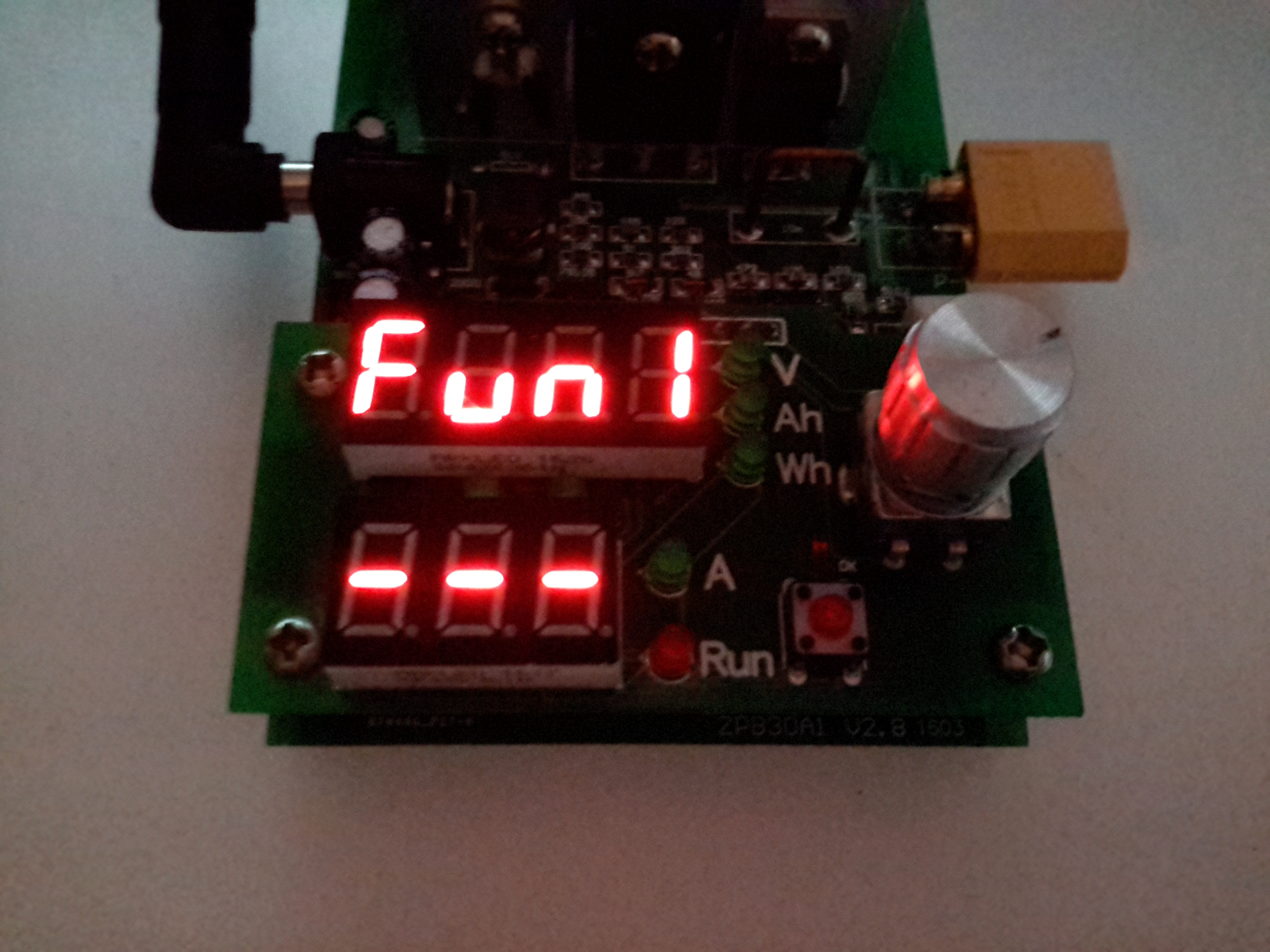
Function 1 – DC Load
Powering the device up while holding the RUN button gets you into the menu to select the operating modes. Function 1 is simple DC load.
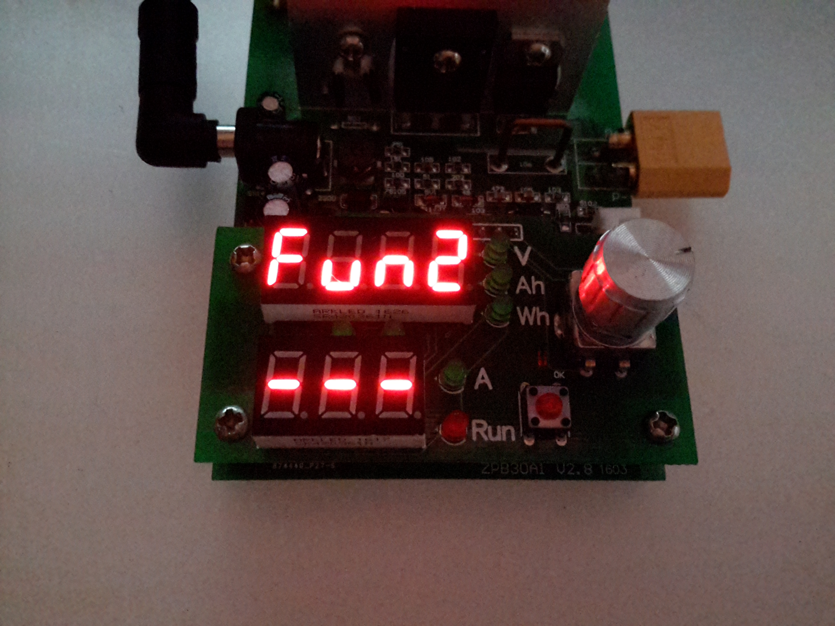
Function 2 – Battery Capacity Mode
The rotary encoder is used to select the option. Function 2 is battery capacity test mode.
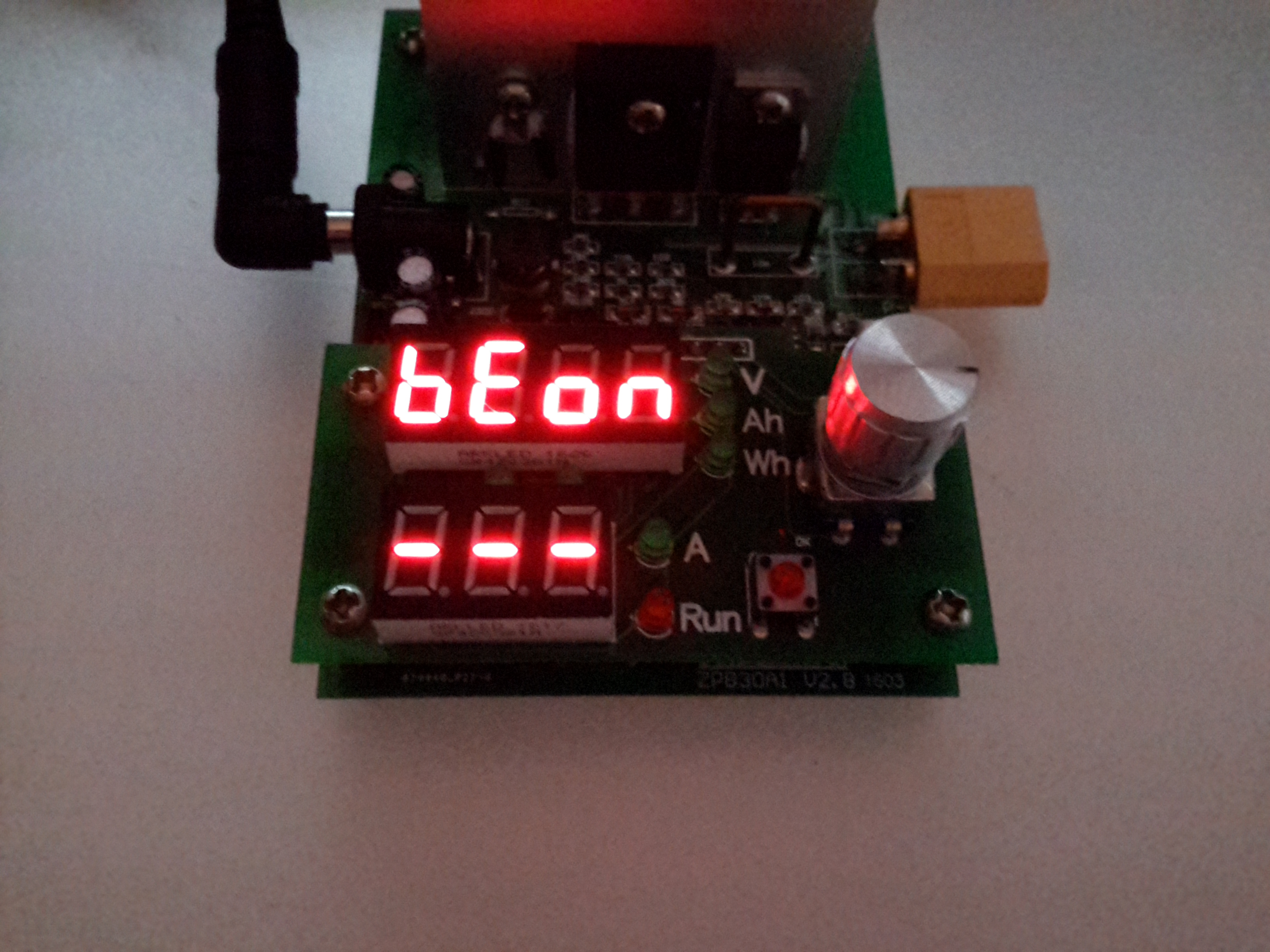
Beeper Mode
After the mode is selected, an option appears to either turn the beeper on or off.
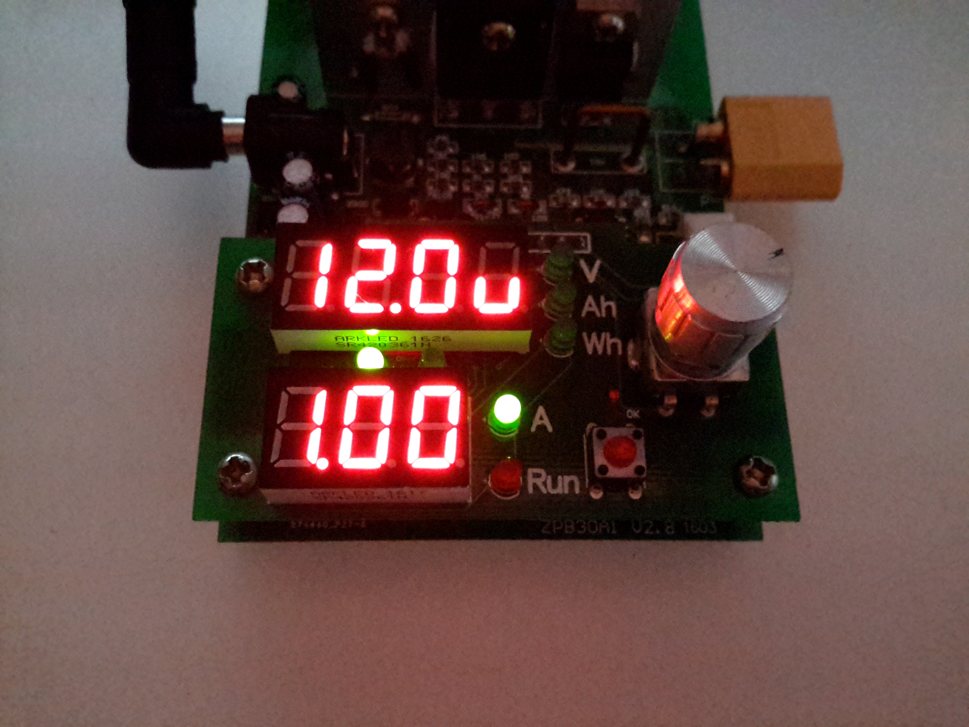
Amps Set
When in standby mode, the threshold voltage & the load current can be set. Here the Amps LED is lit, so the load current can be set. The pair of LEDs between the displays shows which digit will be changed. Pressing the encoder button cycles through the options.
Volts Set
With the Volts LED lit, the threshold voltage can be changed.
When in DC load mode (Fun1), the device will place a fixed load onto the power source until it’s manually stopped. The voltage setting in this mode is a low-voltage alarm. The current can be changed while the load is running.
When in battery discharge test mode (Fun2), the voltage set is the cutoff voltage – discharge will stop when this is reached. Like the DC load mode, the current can be changed when the load is running. After the battery has completed discharging, the capacity in Ah & Wh will be displayed on the top 7-segment. These results can be selected between with the encoder.
Below are tables with all the options for the unit, along with the error codes I’ve been able to decipher from the Chinese info available in various places online. (If anyone knows better, do let me know!).
Option
Function
Fun1
Basic DC Load
Fun 2
Battery Capacity Test
BeOn
Beeper On
BeOf
Beeper Off
Error Code
Meaning
Err1
Input Overvoltage
Err2
Low Battery Voltage / No Battery Present / Reverse Polarity
Err3
Battery ESR Too High / Cannot sustain selected discharge current
Err4
General Failure
Err6
Power Supply Voltage Too Low / Too High. Minimum 12v 0.5A.
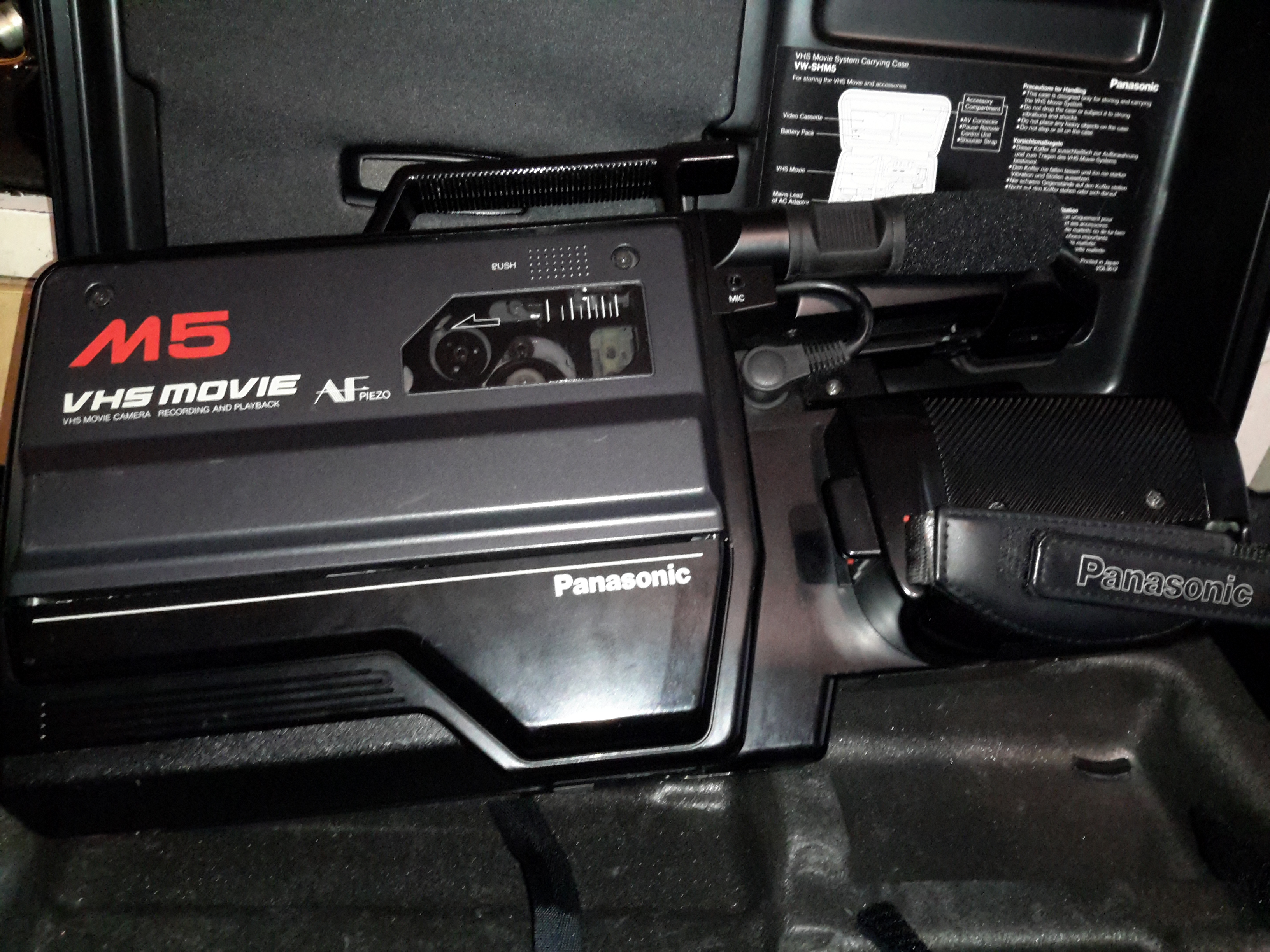
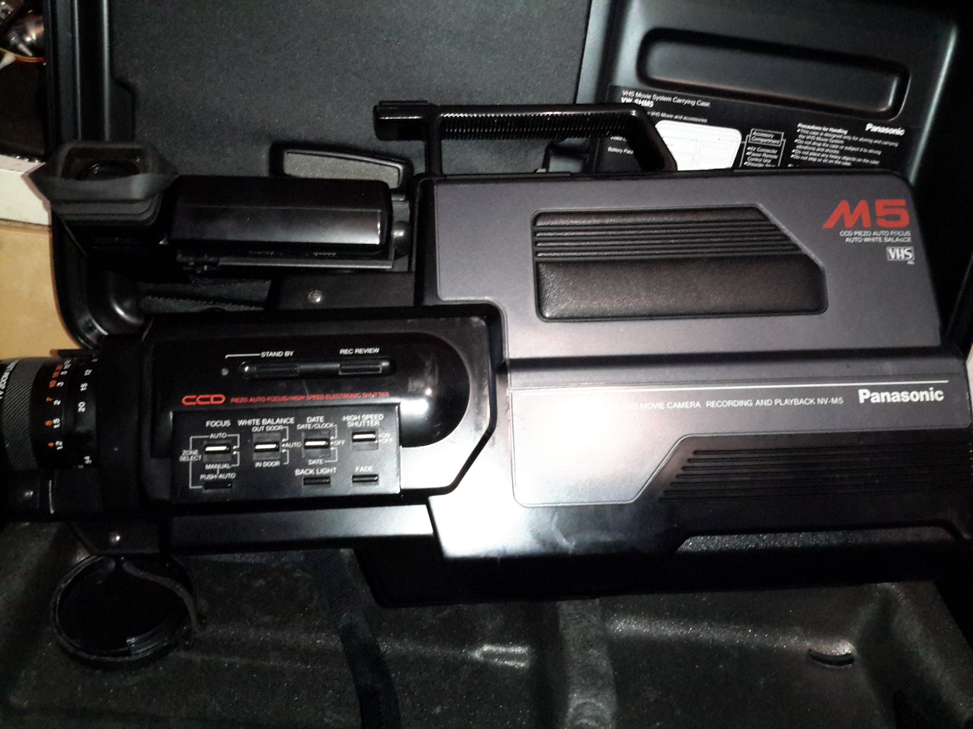
Time foe some more retro tech! This is a 1980’s vintage CCD-based VHS camcorder from Panasonic, the NV-M5. There are a lot of parts to one of these (unlike modern cameras), so I’ll split this post into several sections to make things easier to read (and easier to keep track of what I’m talking about :)).
Left Side
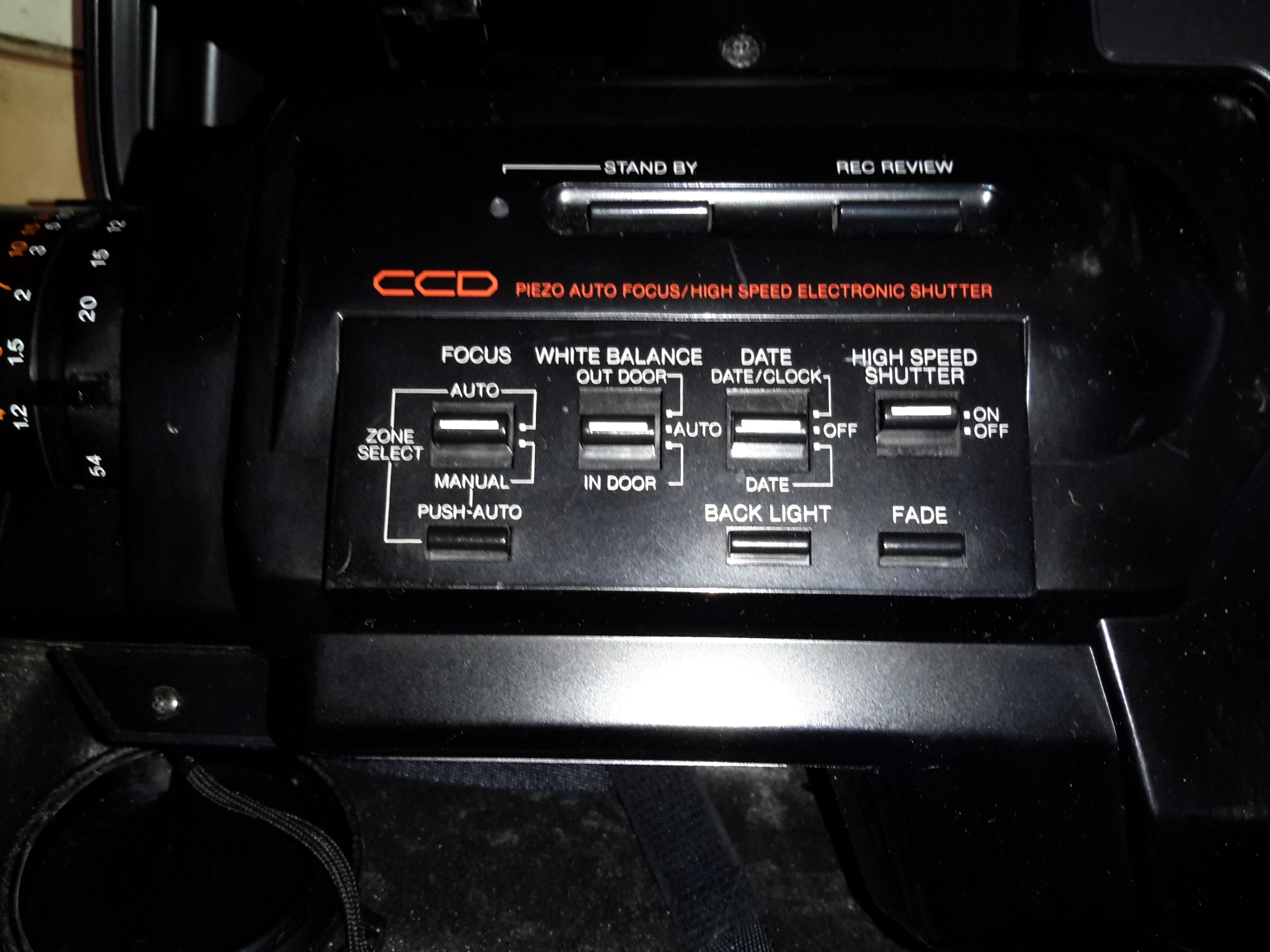
The left side of the camera holds the autofocus, white balance, shutter speed & date controls.
Left Side ControlsLens Adjustments
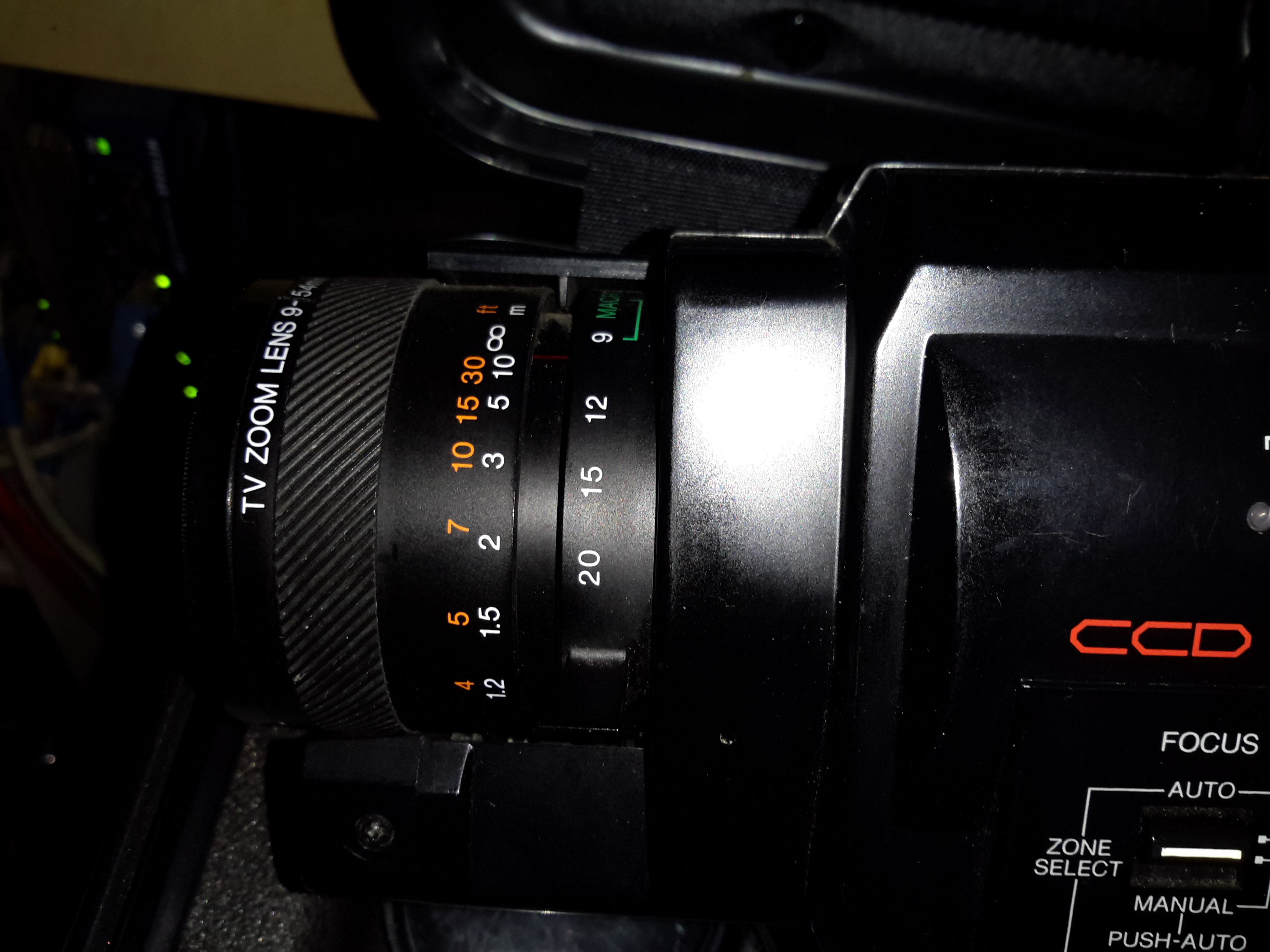
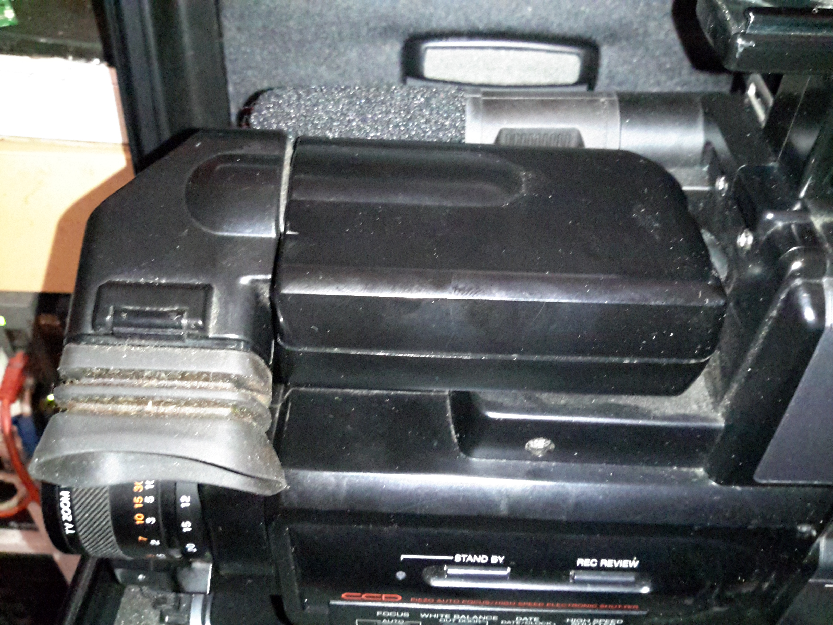
The lens is fully adjustable, with either manual or motorized automatic control.
Rear Panel
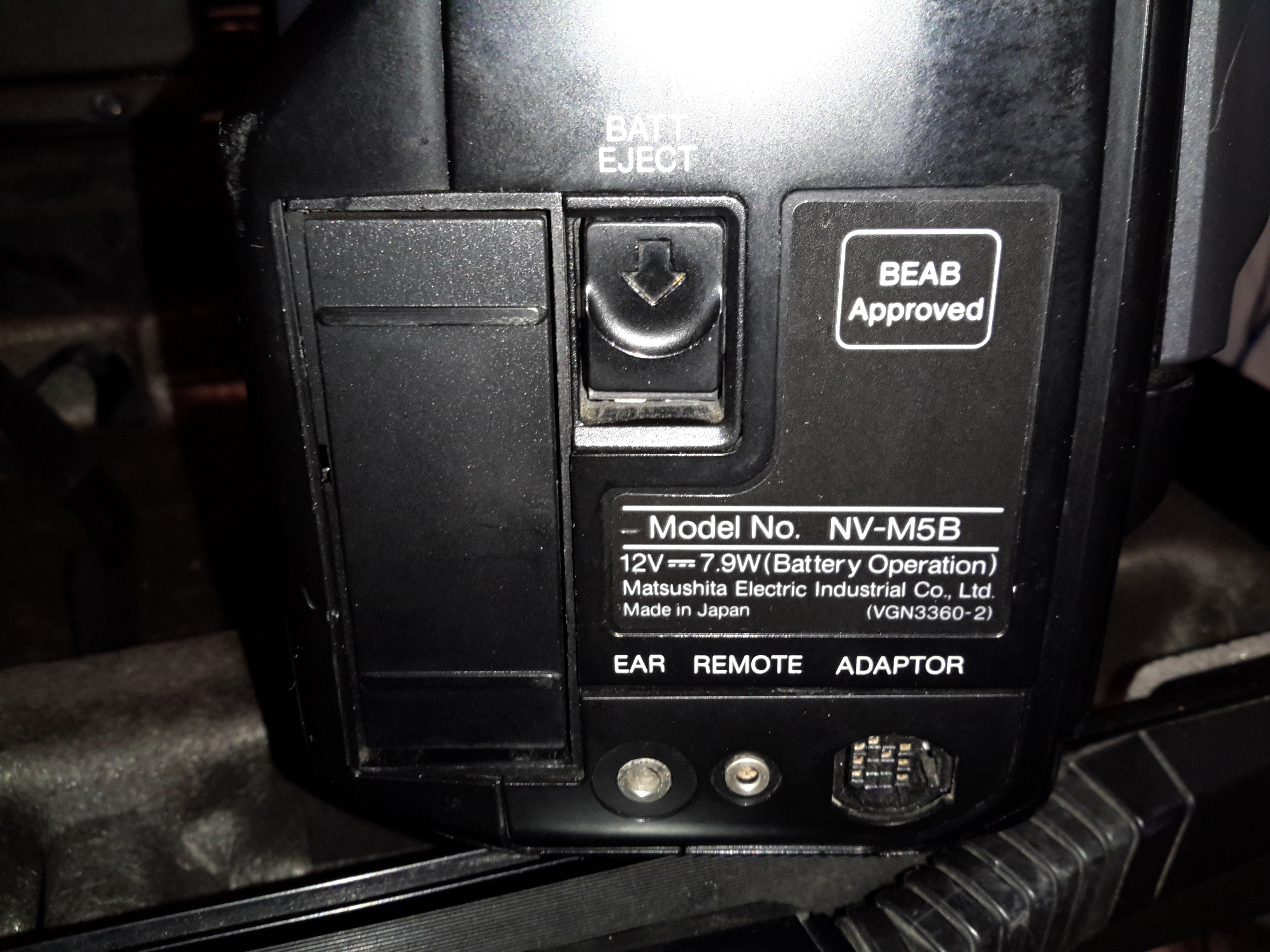
The back panel has the battery slot, a very strange looking DC input connector, remote control connector & the earphone jack.
Top Controls
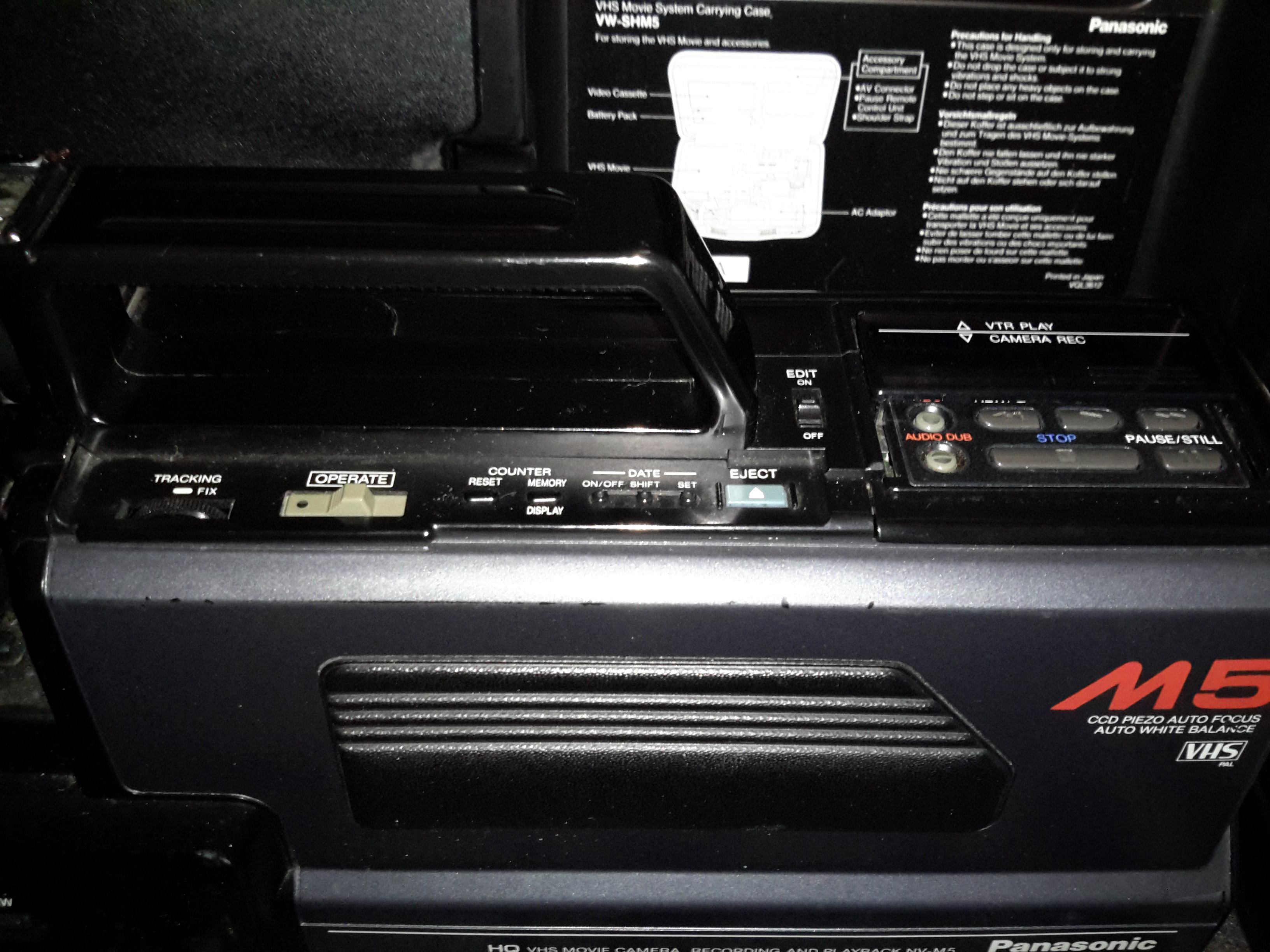
The top panel of the camera holds the main power controls, manual tape tracking & the tape transport control panel.
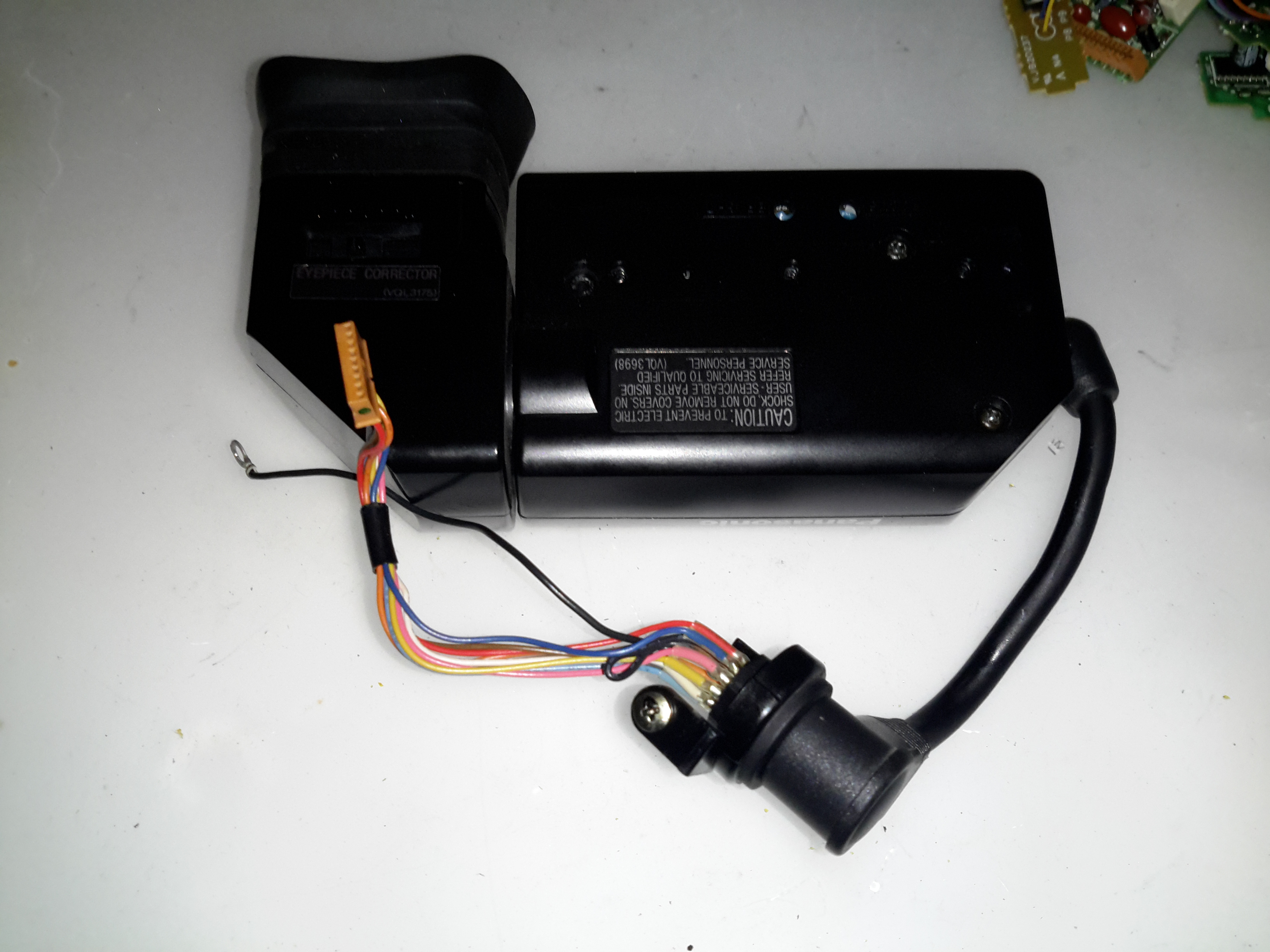
Viewfinder
The viewfinder is mounted on a swivel mount. There’s a CRT based composite monitor in here. Hack ahoy!
Camera Section
Process Board Assembly
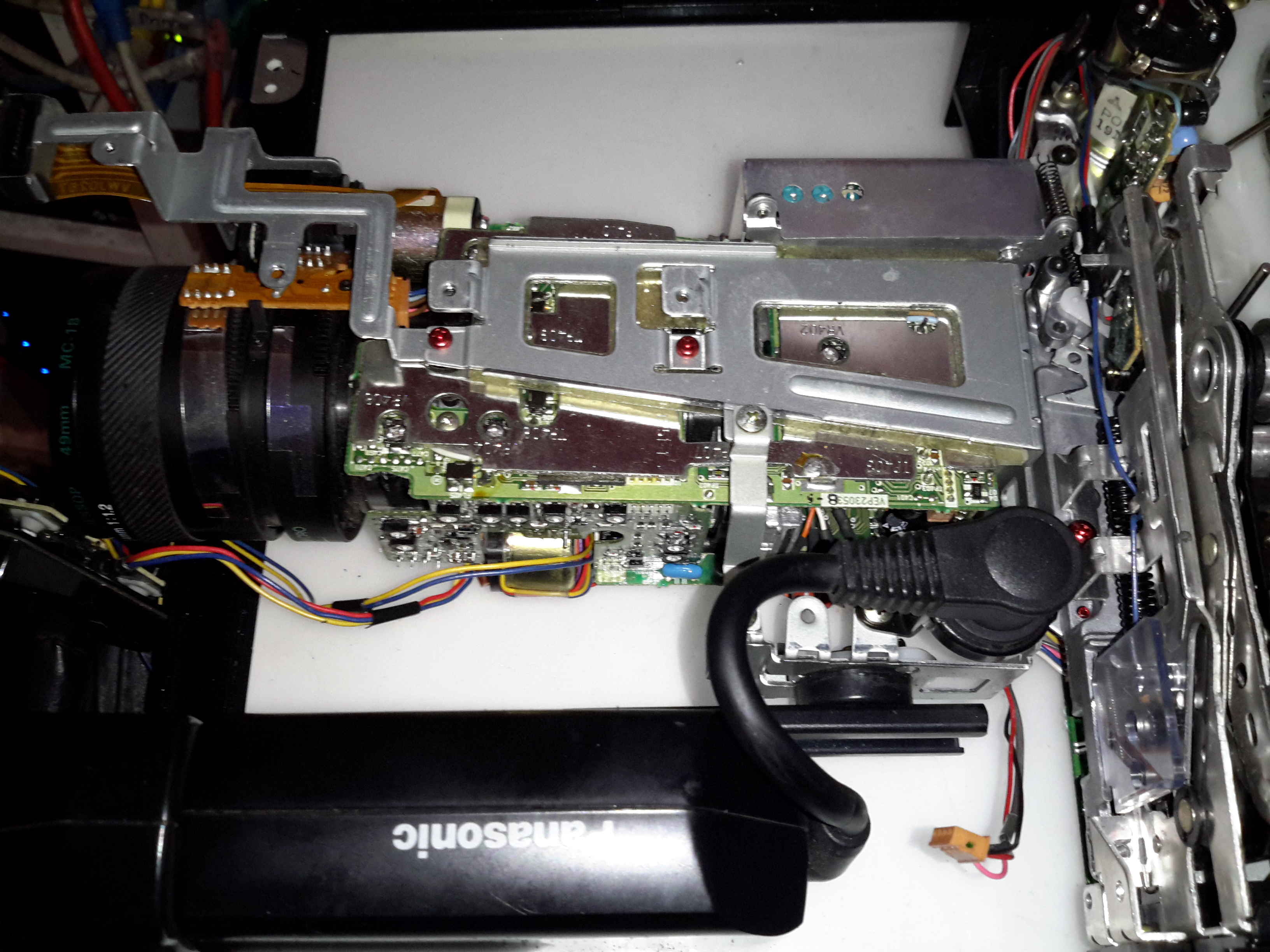
Here’s the camera section of the camcorder, and is totally packed with electronics! There’s at least half a dozen separate boards in here, all fitted together around the optics tube assembly.
AWB PCB
On the top of the assembly is the Automatic White Balance PCB. Many adjustments here to get everything set right. Not much on the other side of this board other than a bunch of Op-Amps. The iris stepper motor is fitted in a milled opening in the PCB, this connects to one of the other PCBs in the camera module.
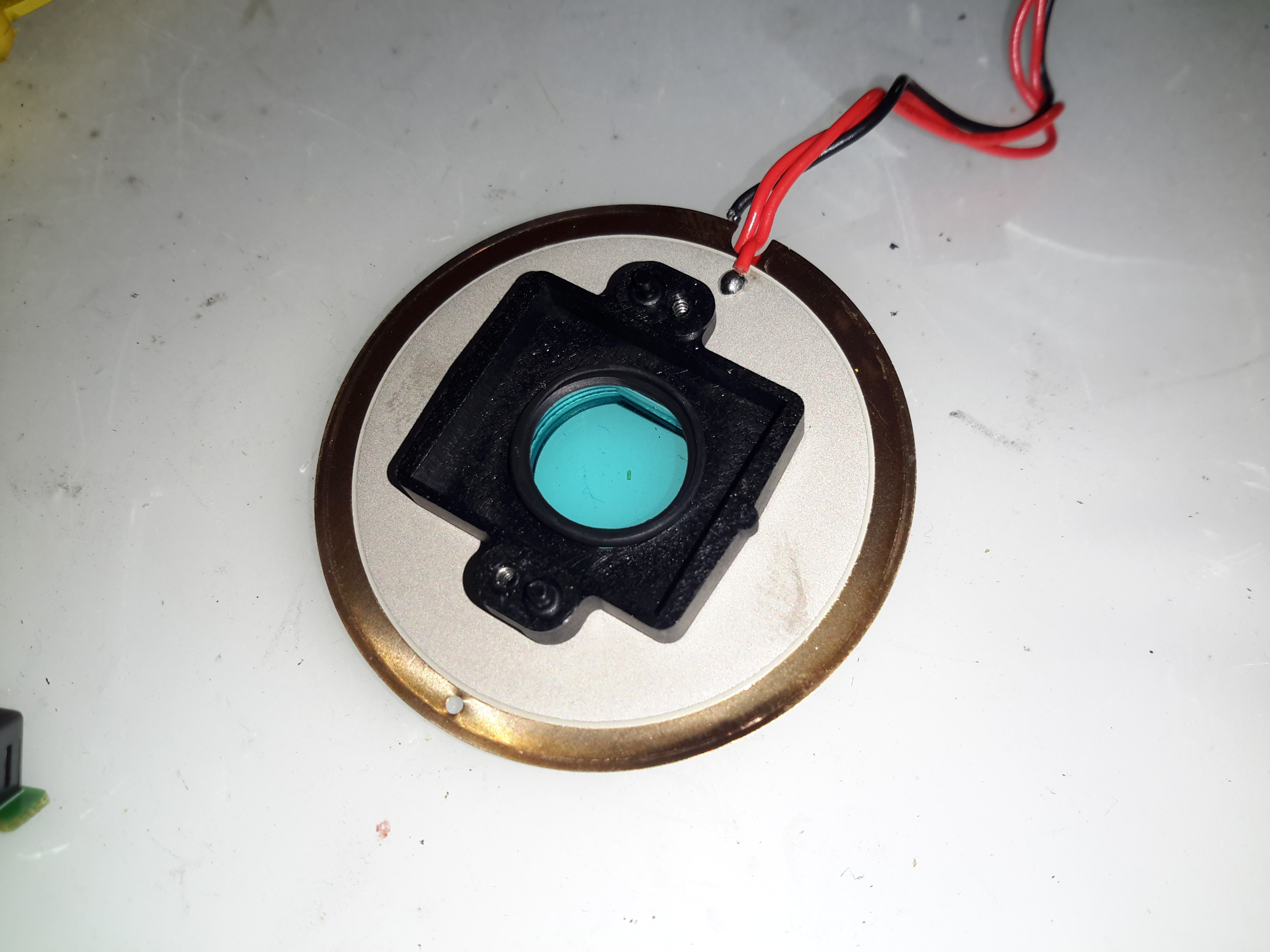
AWB Sensor
Here’s the AWB sensor, mounted next to the lens. I’m not all to certain how this works, but the service manual has the pinout, and there are outputs for all the colour channels, RGB. So it’s probably a trio of photodiodes with filters.
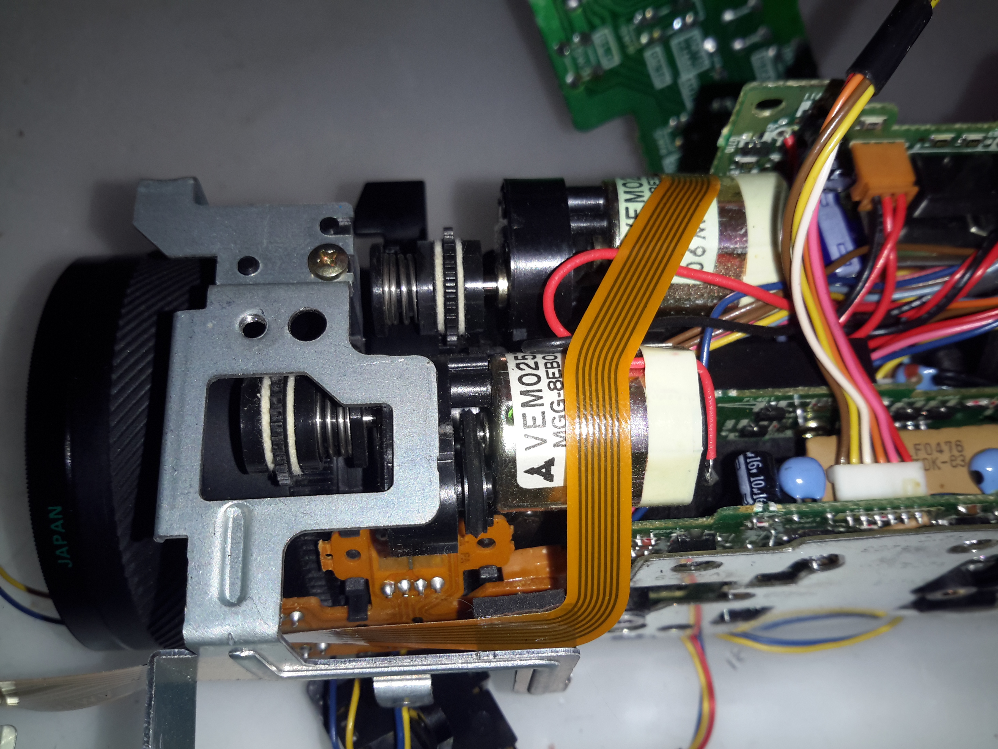
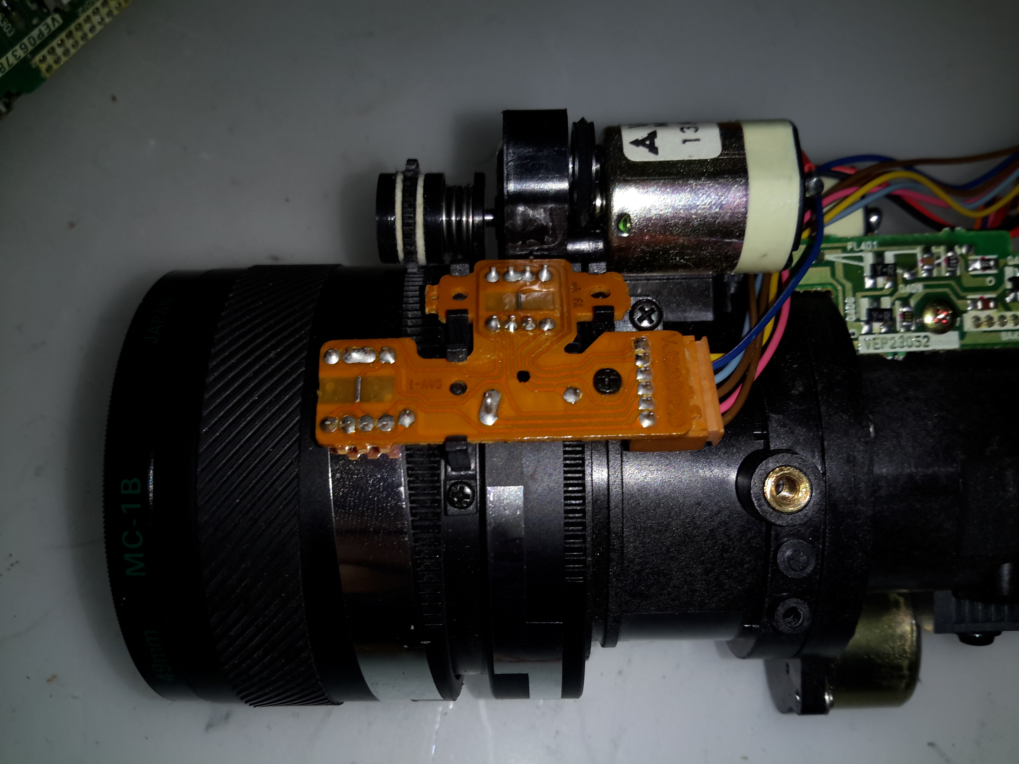
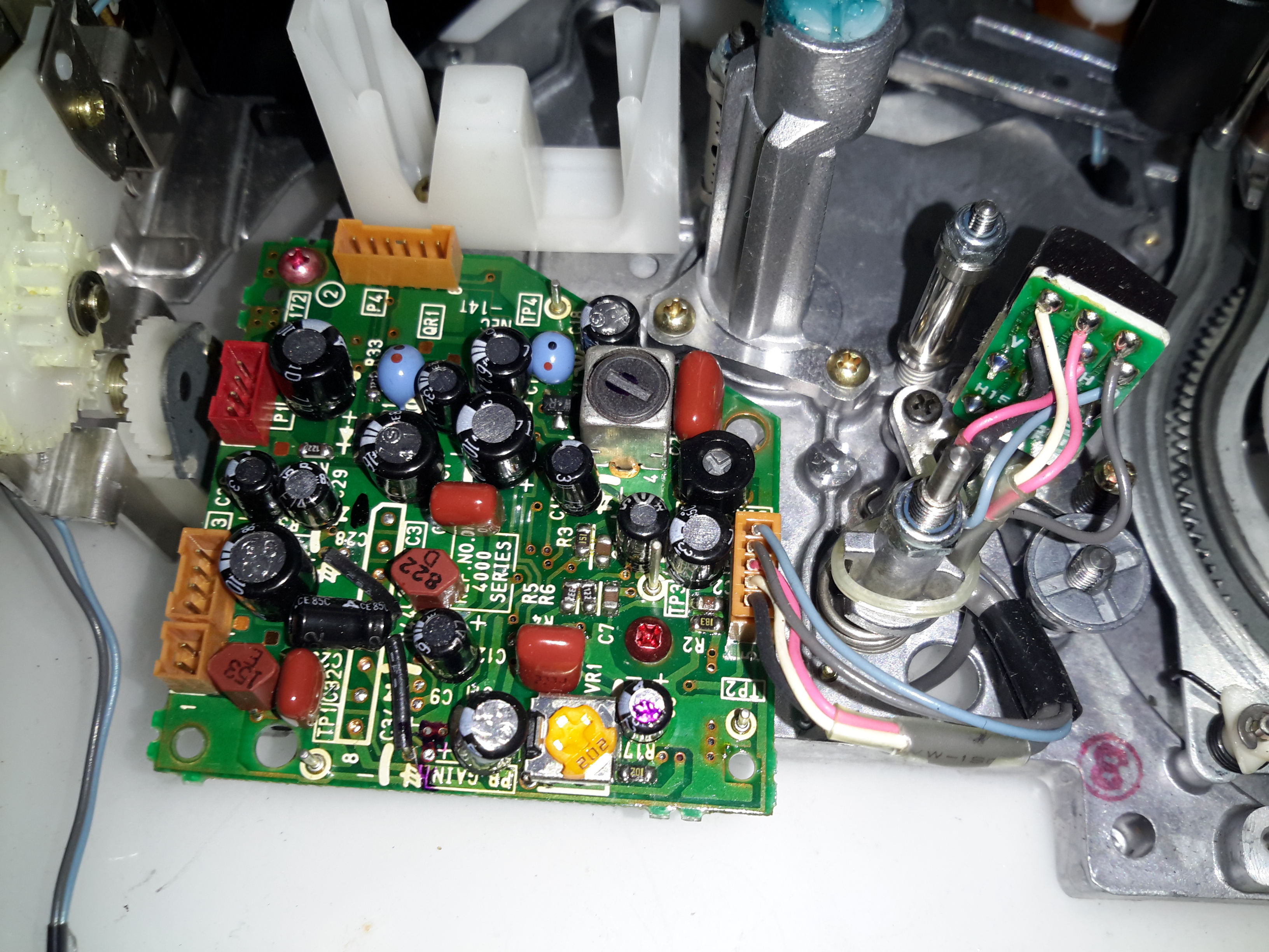
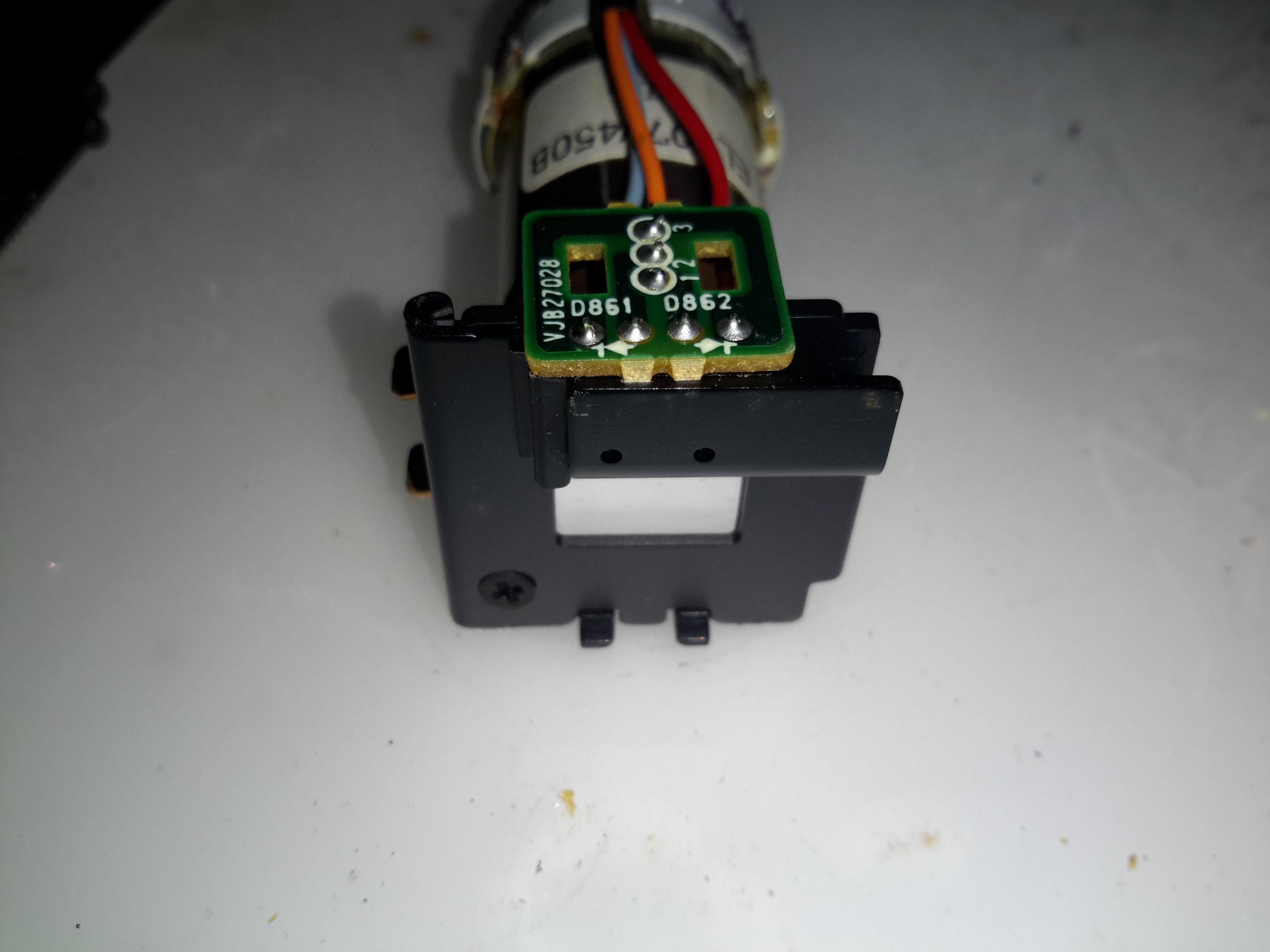
Focus & Zoom Motors
Focus & Zoom are controlled with a pair of DC gear motors. The manual operation is feasible through the use of slip clutches in the final drive pinion onto the lens barrel.
Process Board
The main camera section process board is above. This board does all the signal processing for the CCD, has the bias voltage supplies and houses the control sections for the motorized parts of the optics assembly. There are quite a few dipped Tantalum capacitors on pigtails, instead of being directly board mounted. This was probably done due to space requirements on the PCB itself.
Under the steel shield on this board is some of the main signal processing for the CCD.
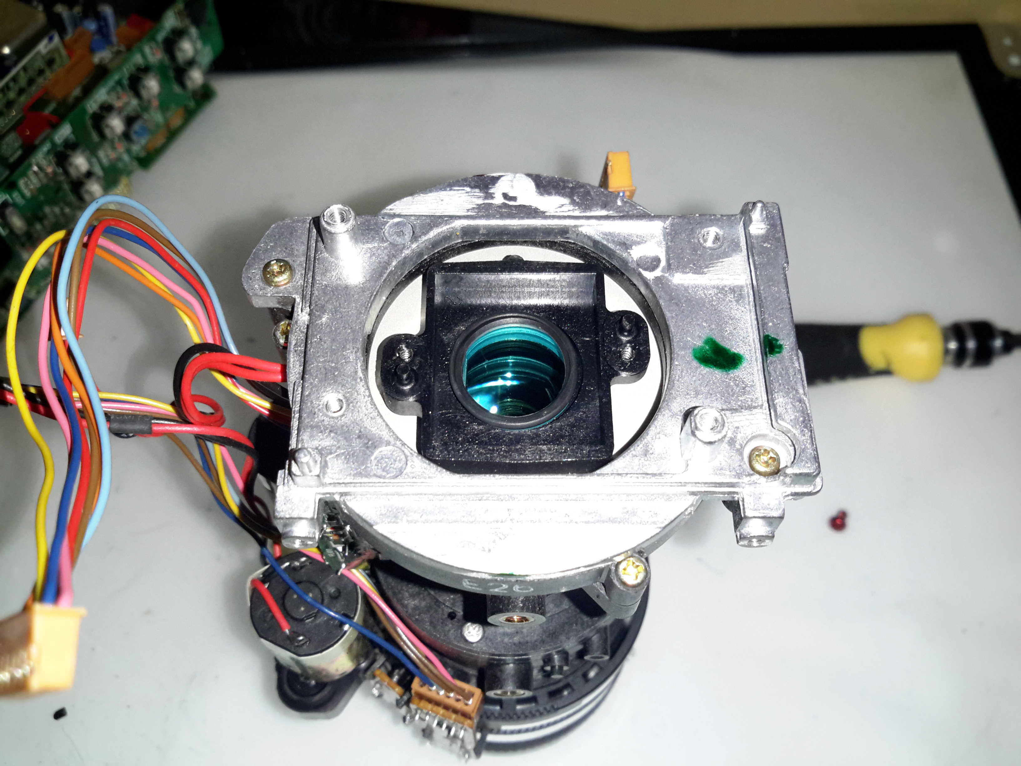
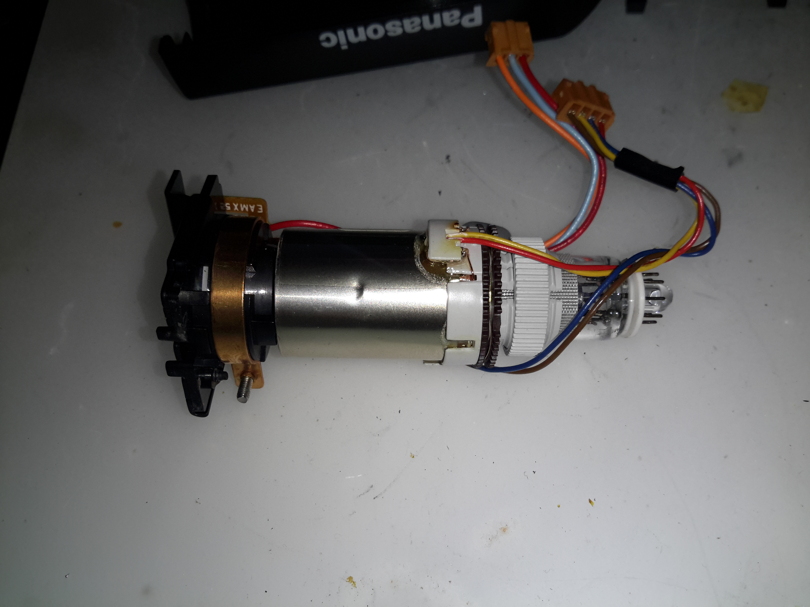
Optics Assembly
The back of the optics tube is a heavy casting, to supress vibration. This will be more clear later on.
Position Sensor Flex
The position of the lens elements is determined by reflective strips on the barrel & sensors on this flex PCB.
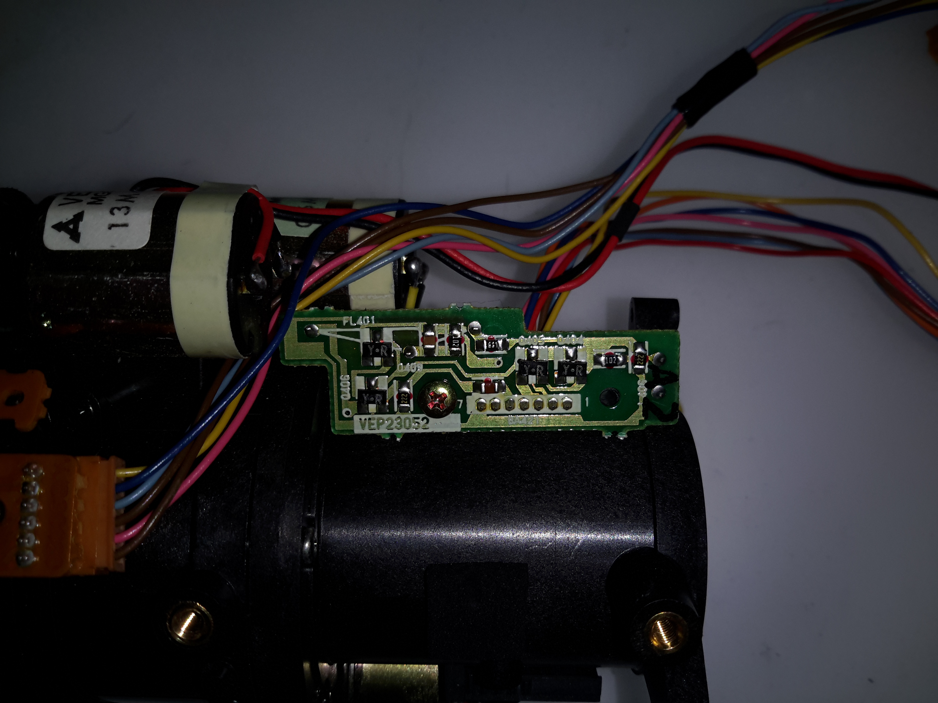
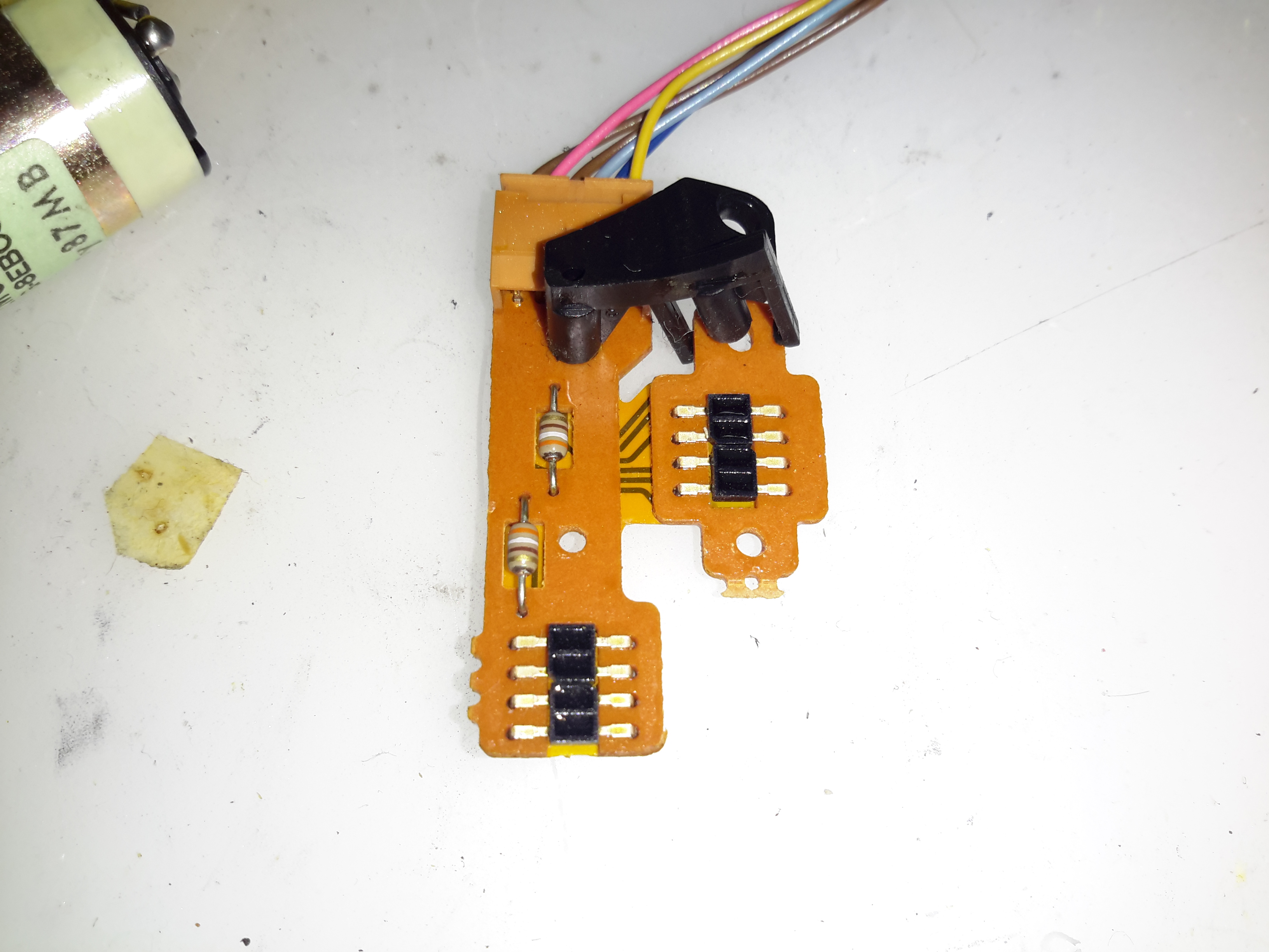
Sub Process Board
There’s another small board tucked into the side of the tube, this hooks into the process PCB.
Process Delay Line
According to the schematic, there’s nothing much on this board, just a delay line & a few transistors.
Piezo Focus Disc
Here’s the reason for the heavy alloy casing at the CCD mounting end of the optics: the fine focus adjustment is done with a piezoelectric disc, the entire CCD assembly is mounted to this board. Applying voltage to the electrodes moves the assembly slightly to alter the position of the CCD. The blue glass in the centre of the unit is the IR filter.
IR Relective Sensors
The barrel position sensors are these IR-reflective type.
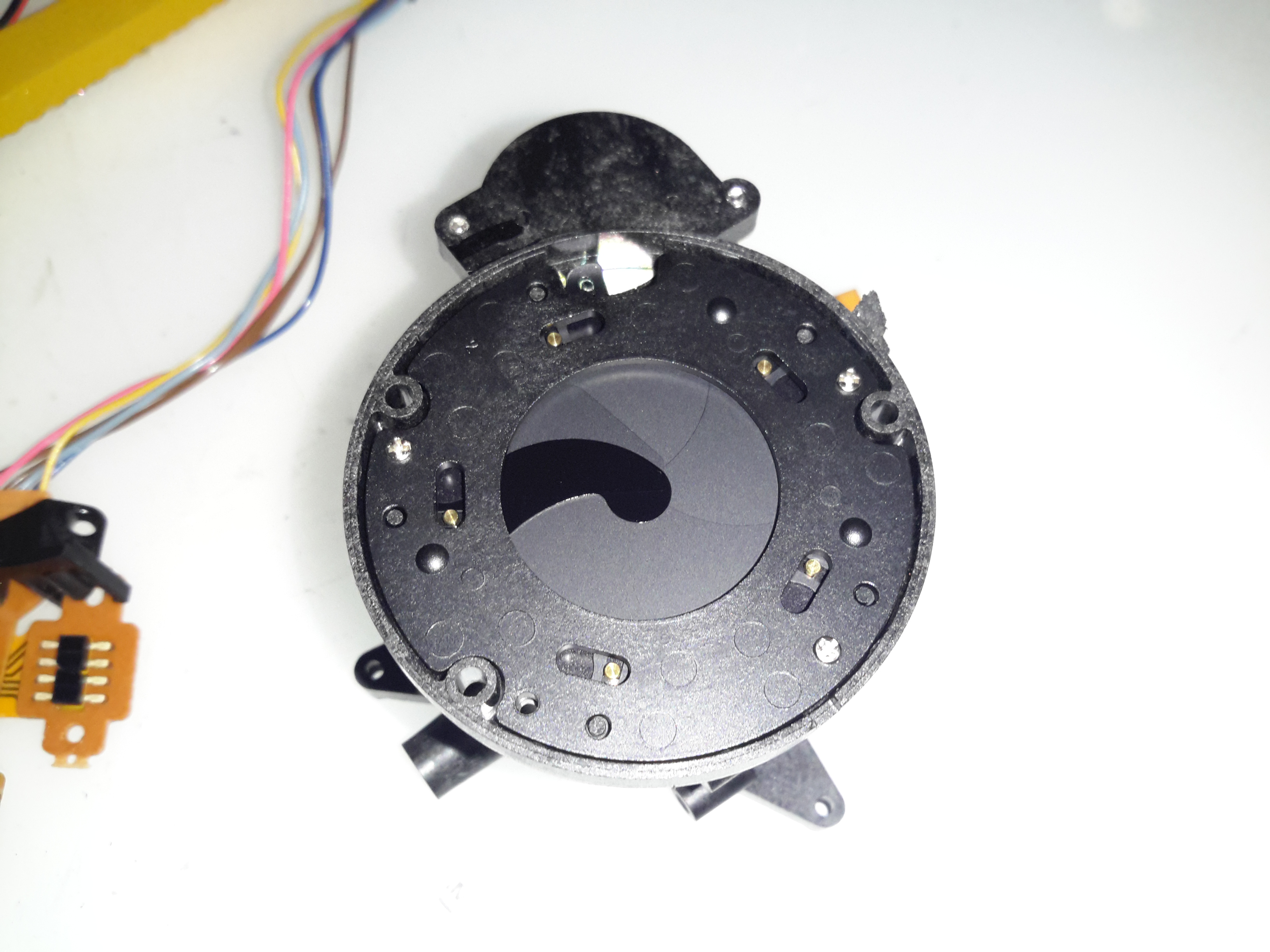
Iris Assembly
The iris is mounted just before the CCD, this is controlled with a galvanometer-type device with position sensors incorporated.
Iris Opening
Pushing on the operating lever with the end of my screwdriver opens the leaves of the iris against the return spring.
Tape Transport & Main Control
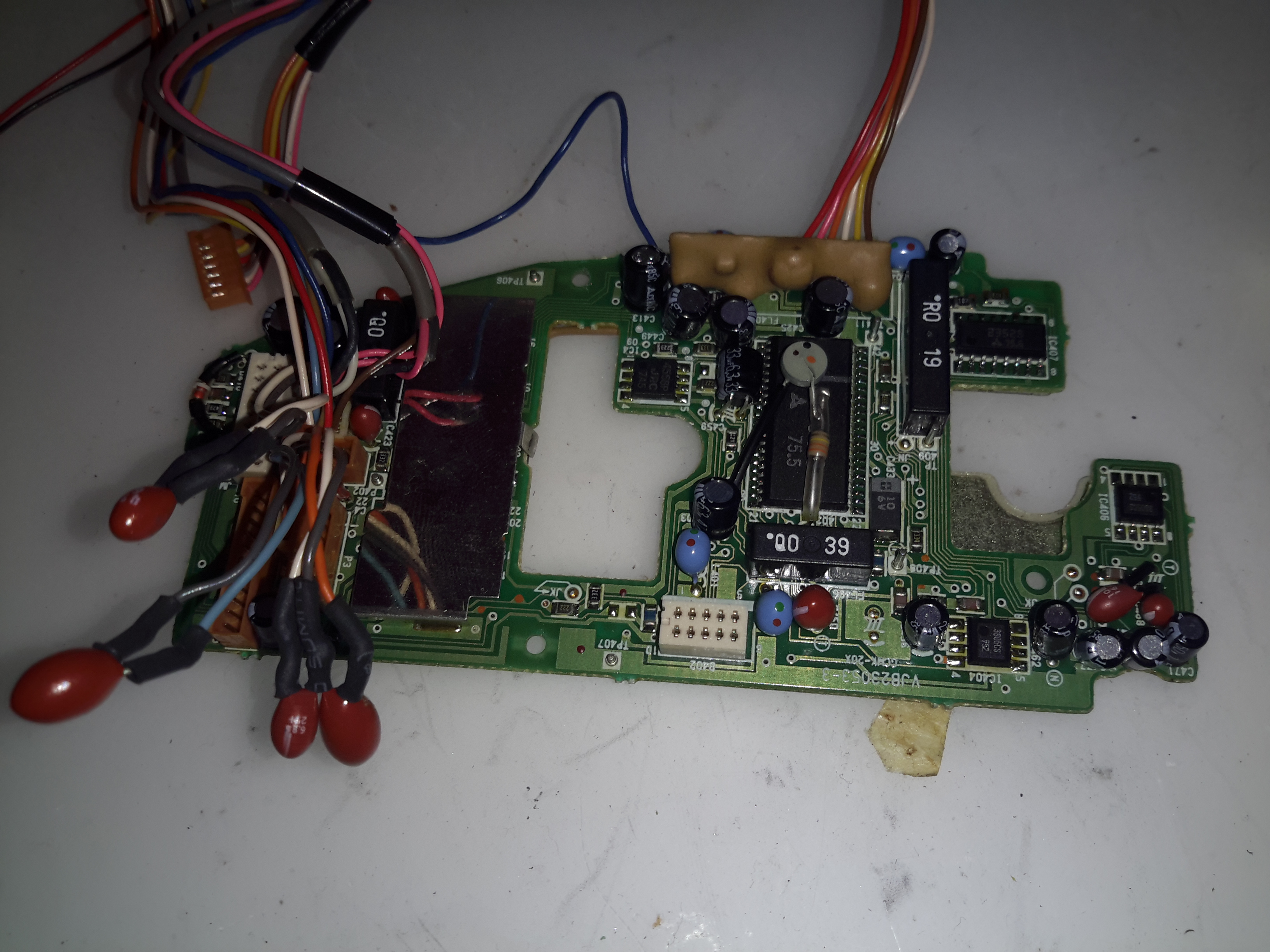
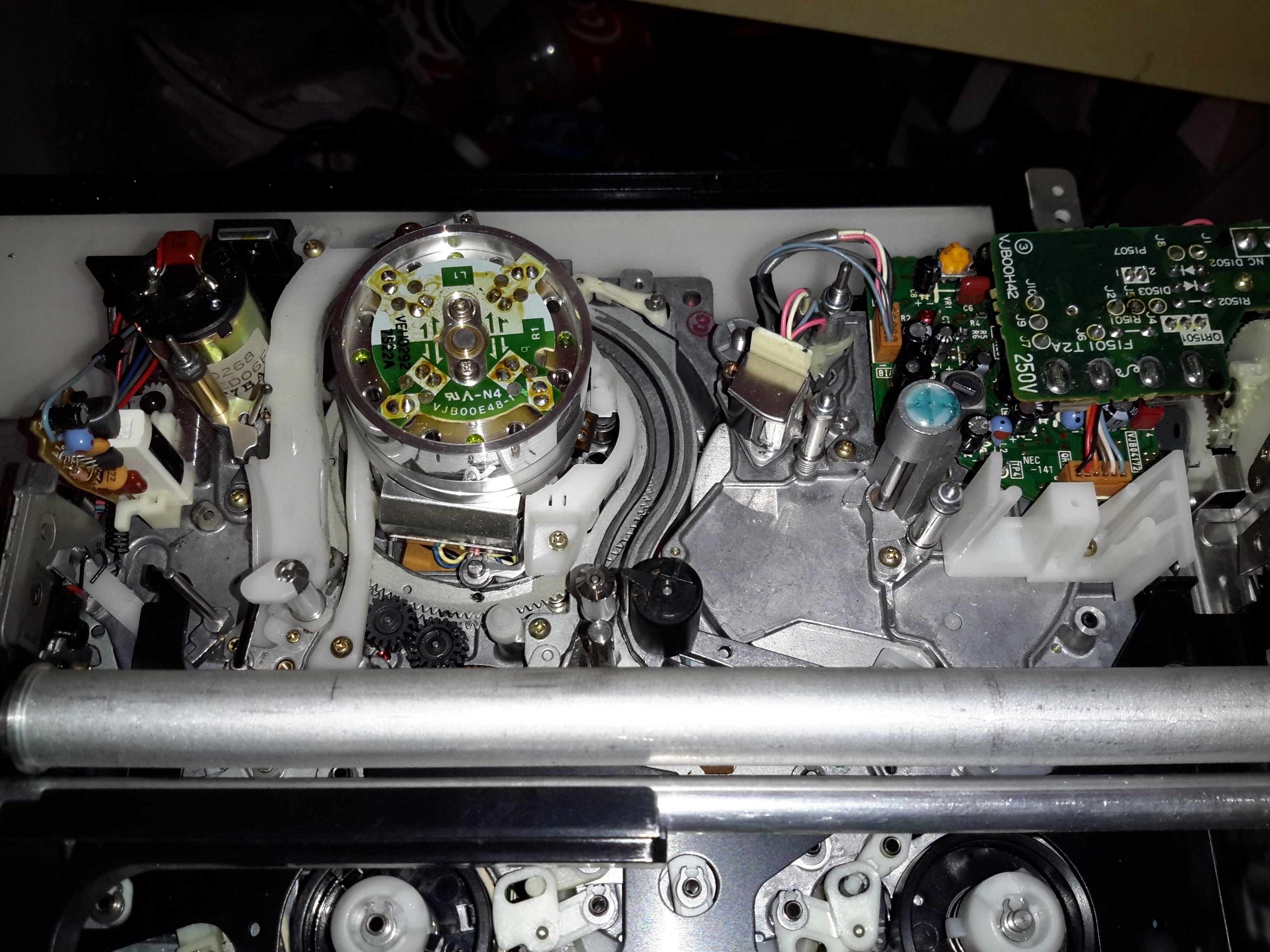
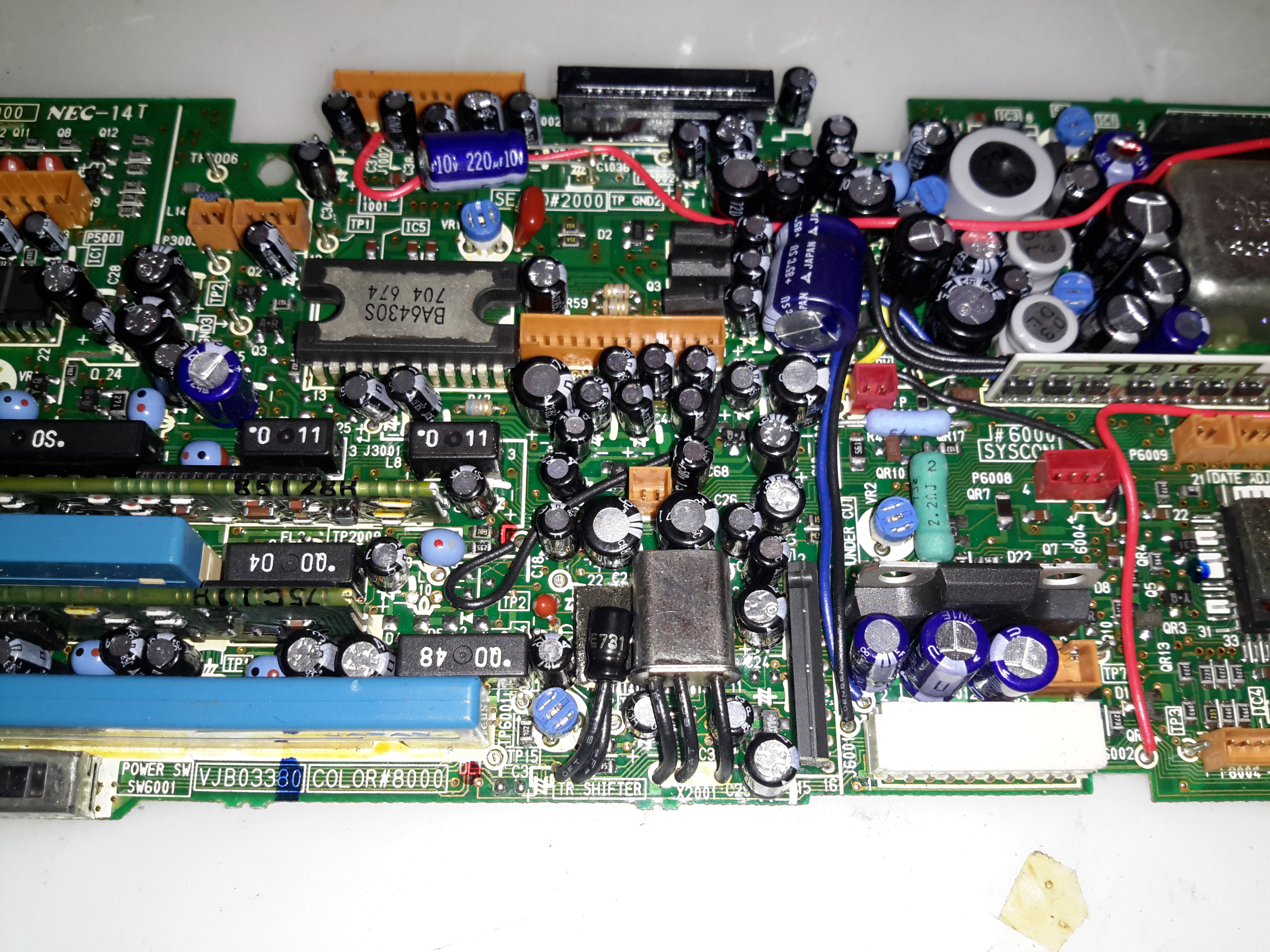
Main Control Board
Tucked into the side of the main body of the unit is the main system control board. This PCB houses all the vital functions of the camera: Power Supply, Servo Control, Colour Control,Video Amplifiers, etc.
Tape Drum
Here’s the main tape transport mechanism, this is made of steel & aluminium stampings for structural support. The drum used in this transport is noticeably smaller than a standard VHS drum, the tape is wrapped around more of the drum surface to compensate.
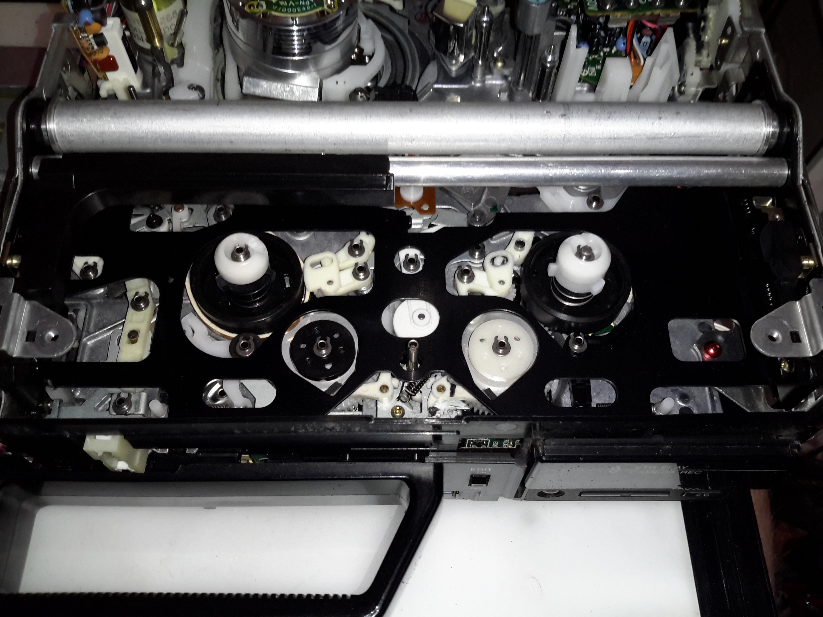
Tape Transport
The VHS tape sits in this carriage & the spools drive the supply & take up reels in the cartridge.
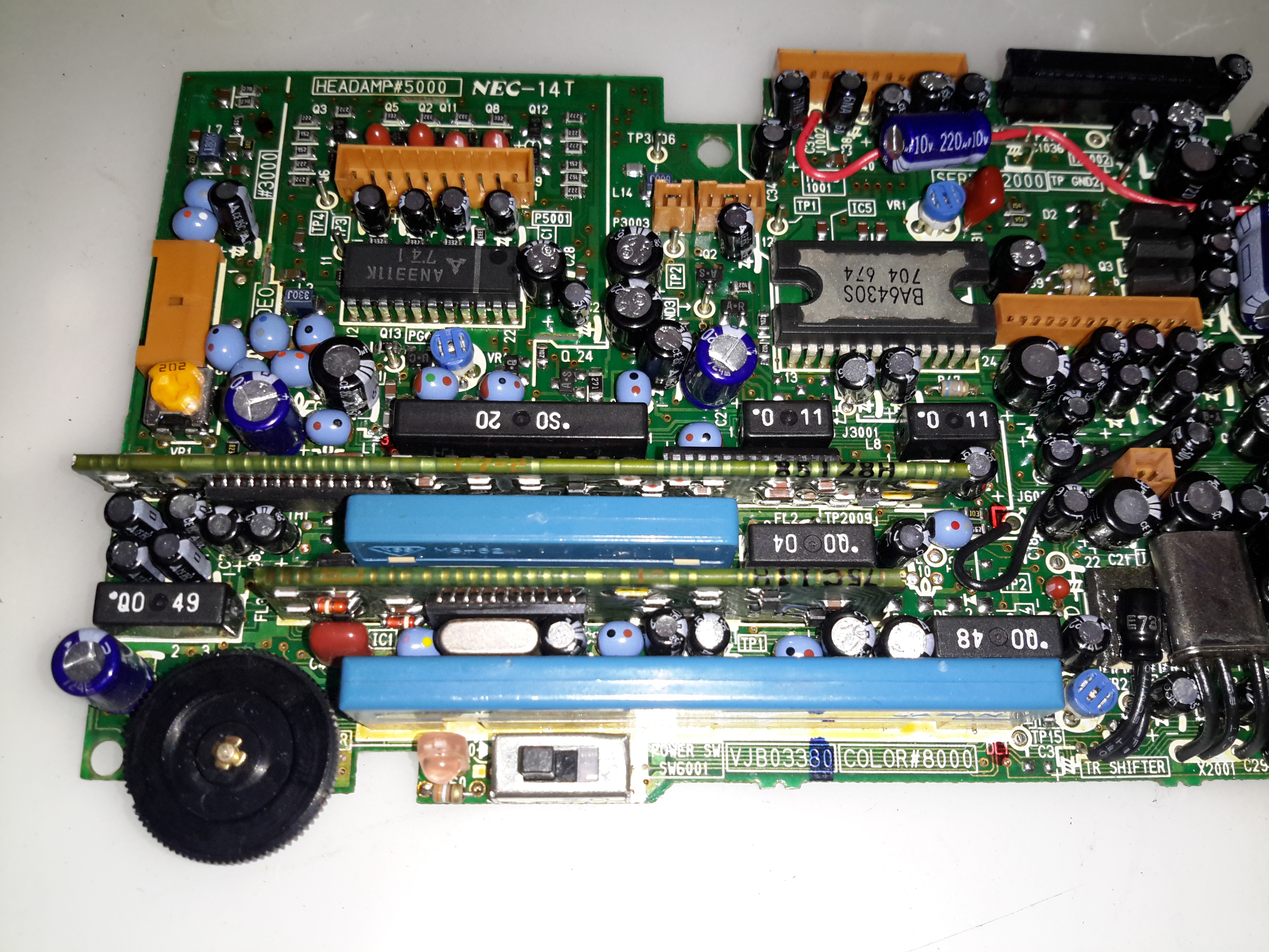
Main Control PCB
Here’s the component side of the main control PCB. This one is very densely packed with parts, I wouldn’t like to try & troubleshoot something like this!
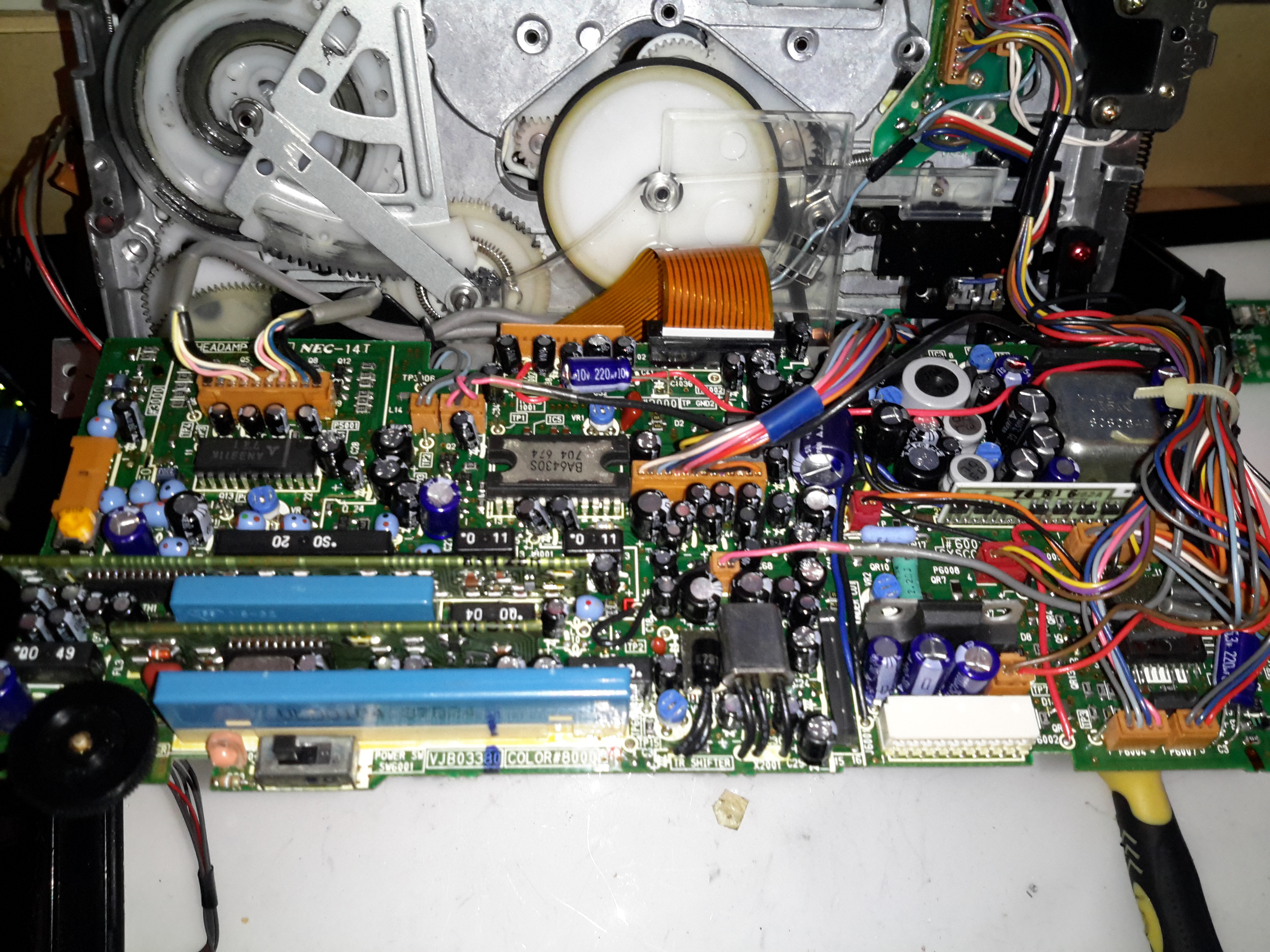
Main PCB Left
The left side has the video head amp at the top, a Panasonic AN3311K 4-head video amp. Below that is video processing, the blue components are the analogue delay lines. There are a couple of hybrid flat-flex PCBs tucked in between with a couple of ICs & many passives. These hybrids handle the luma & chroma signals.
Top left is the capstan motor driver a Rohm BA6430S. The transport motors are all 3-phase brushless, with exception of the loading motor, which is a brushed DC type.
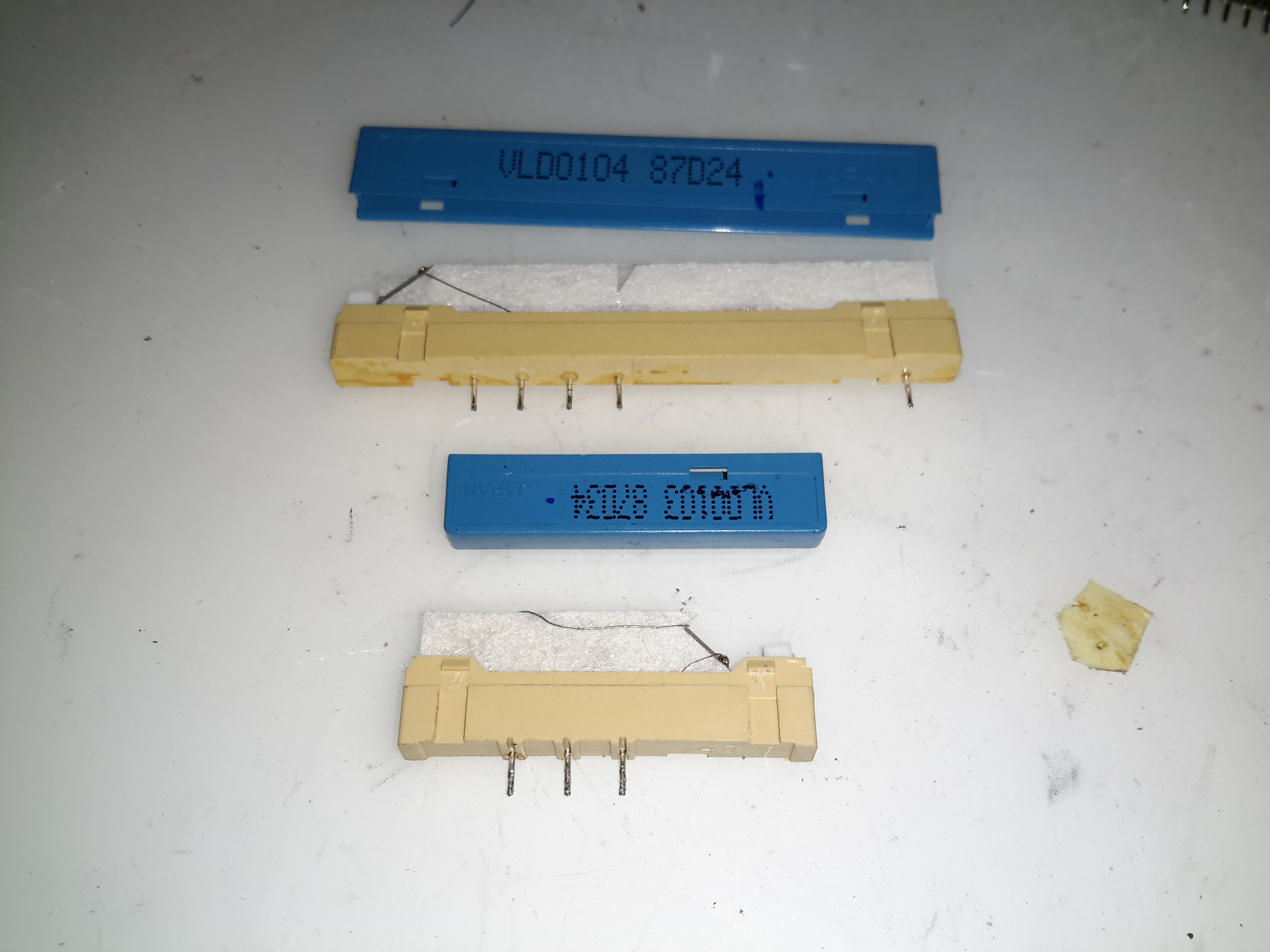
Delay Line
Here’s what is inside the delay lines for the analogue video circuits. The plastic casing holds a felt liner, inside which is the delay line itself.
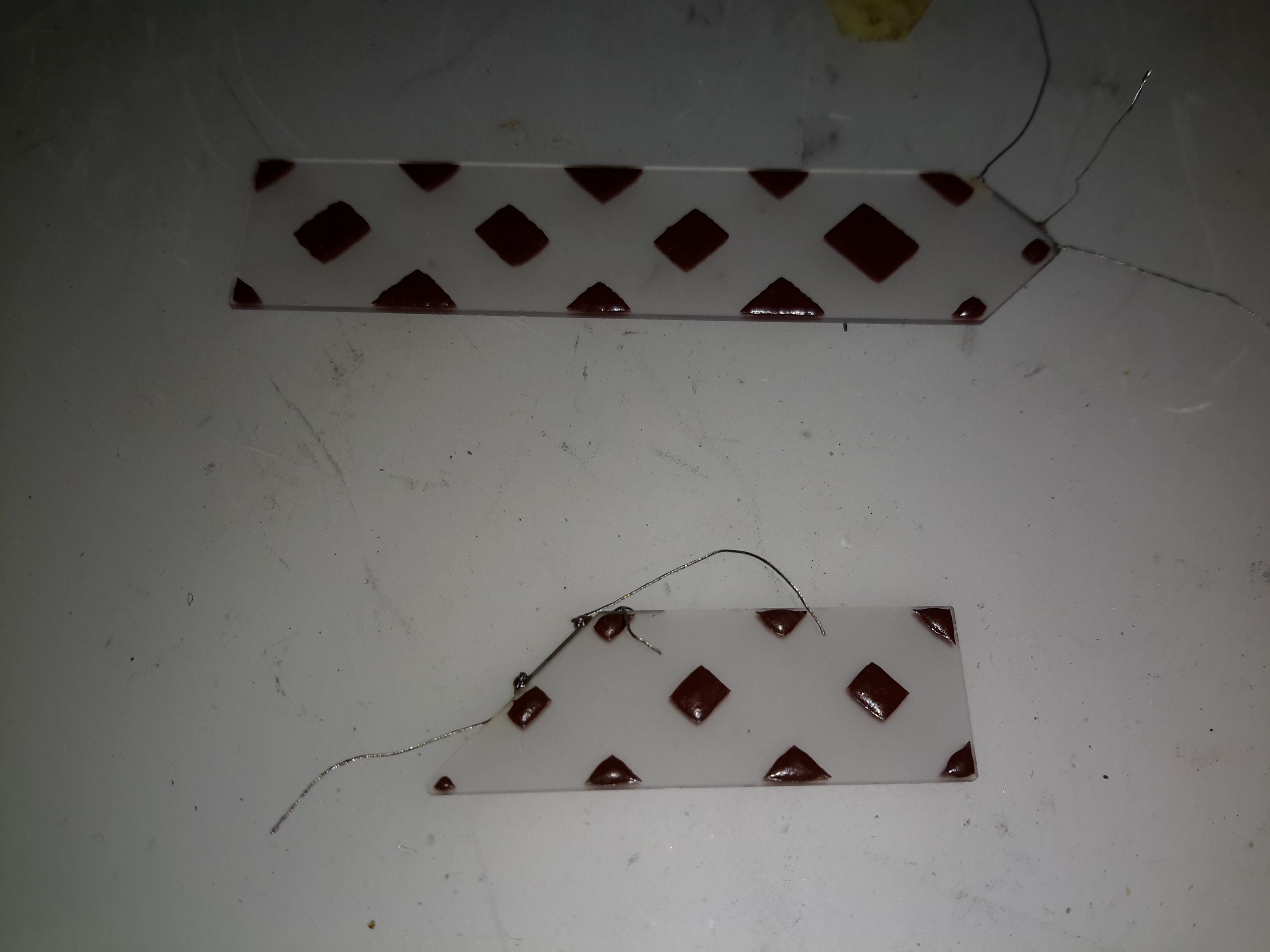
Internal Glass
The delay is created by sending an acoustic signal through the quartz crystal inside the device by a piezoelectric transducer, bouncing it off the walls of the crystal before returning it to a similar transducer.
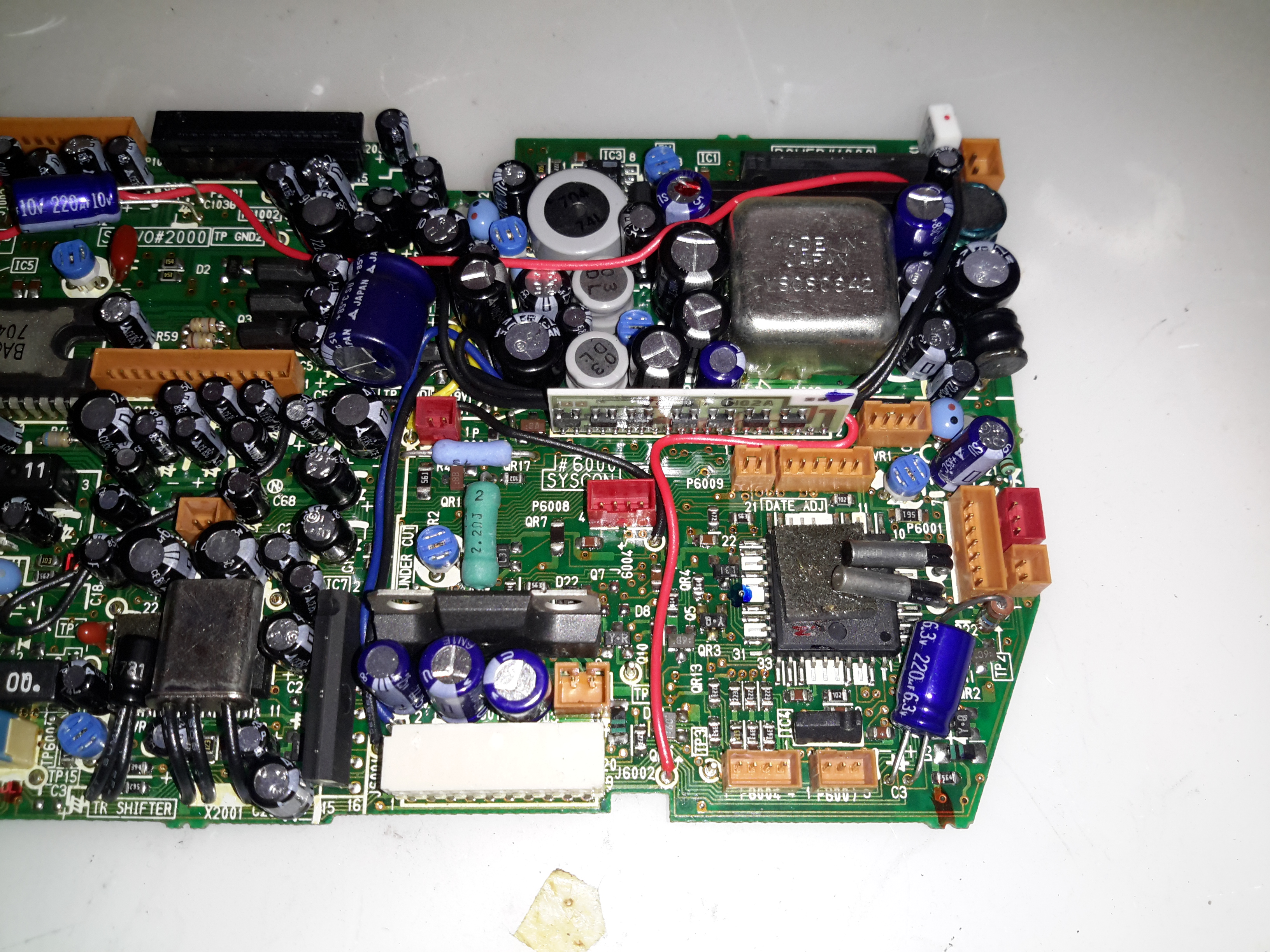
Main PCB Centre
Here’s the centre of the board, the strange crystal at bottom centre is the clock crystal for the head drum servo. Why it has 3 pins I’m not sure, only the two pins to the crystal inside are shown connected on the schematic. Maybe grounding the case?
The main servo controls for the head drum & the capstan motor are top centre, these get a control signal from the tape to lock the speed of the relative components.
Main PCB Right
Here’s the right hand side. The main power supply circuitry is at top right, with a large can containing 4 switching inductors & a ferrite pot core transformer. All these converters are controlled by a single BA6149 6-channel DC-DC converter controller IC via a ULN2003 transistor array.
The ceramic hybrid board next to the PSU has 7 switch transistors for driving various indicator LEDs.
The large tabbed IC bottom centre is the loading motor drive, an IC from Mitsubishi, the M54543. This has bidirectional DC control of the motor & built in braking functions. The large quad flat pack IC on the right is the MN1237A on-screen character generator, with the two clock crystals for the main microcontroller.
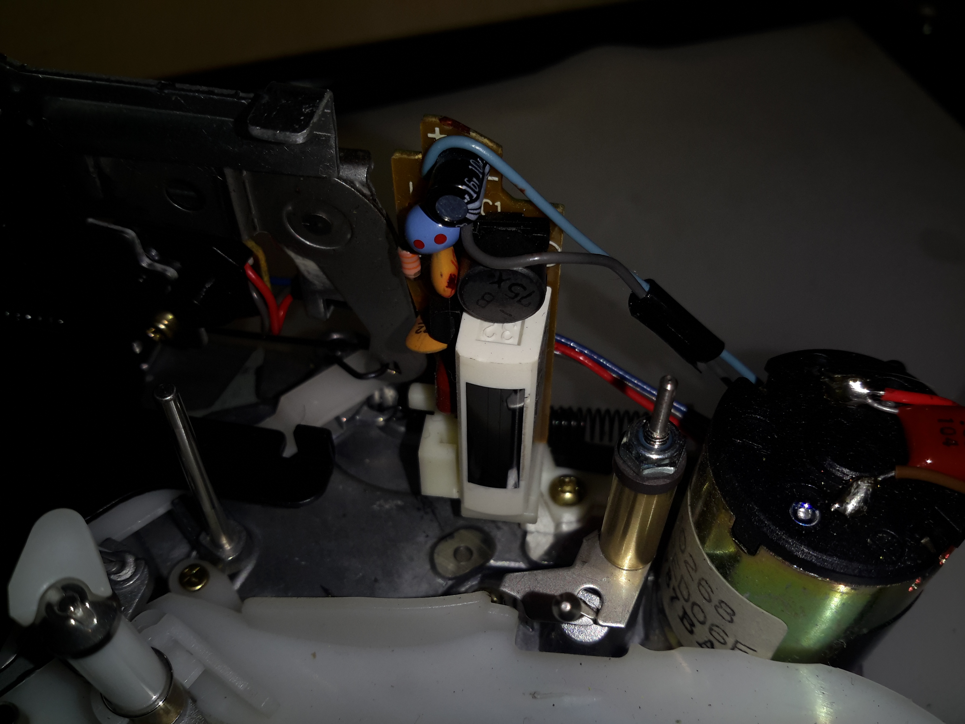
Erase Head
The full erase head has it’s power supply & oscillator on board, applying 9v to this board results in an AC signal to the head, which erases the old recording from the tape before the new recording is laid down by the flying heads on the drum.
Audio Control PCB
The Audio & Control head is connected to this PCB, which handles both reading back audio from the tape & recording new audio tracks. The audio bias oscillator is on this board, & the onboard microphone feeds it’s signal here. The control head is fed directly through to the servo section of the main board.
Drum Motor
The motor that drives the head drum is another DC brushless 3-phase type.
Hall Sensors
These 3 Hall sensors are used by the motor drive to determine the rotor position & time commutation accordingly.
Stator
The stator on this motor is of interesting construction, with no laminated core, the coils are moulded into the plastic holder. The tach sensor is on the side of the stator core. This senses a small magnet on the outside of the rotor to determine rotational speed. For PAL recordings, the drum rotates at 1500 RPM.
Motor Removed
Not much under the stator other than the bearing housing & the feedthrough to the rotary transformer.
Head Disc
The heads are mounted onto the top disc of the drum, 4 heads in this recorder. The signals are transmitted to the rotating section through the ferrite rotary transformer on the bottom section.
Head Chip
The tiny winding of the ferrite video head can just about be seen on the end of the brass mounting.
Capstan Motor Components
The capstan motor is similar to the drum motor, only this one is flat. The rotor has a ferrite magnet, in this case it wasn’t glued in place, just held by it’s magnetic field.
Capstan Motor Stator
The PCB on this motor has a steel backing to complete the magnetic circuit, the coils for the 3 motor phases are simply glued in place. The Hall sensors on this motor are placed in the middle of the windings though.
Again there is a tach sensor on the edge of the board that communicates the speed back to the controller. This allows the servo to remain locked at constant speed.
Viewfinder
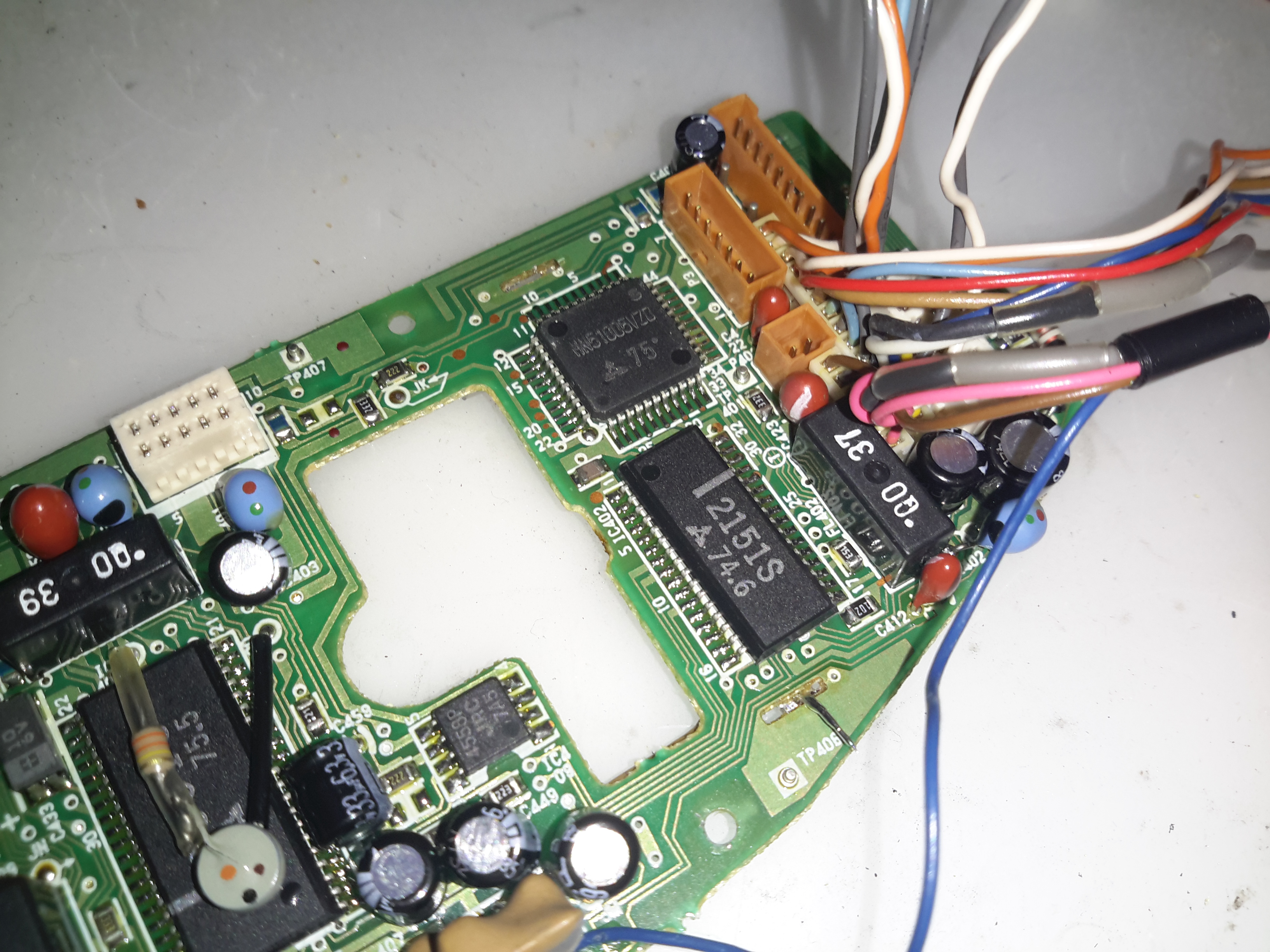
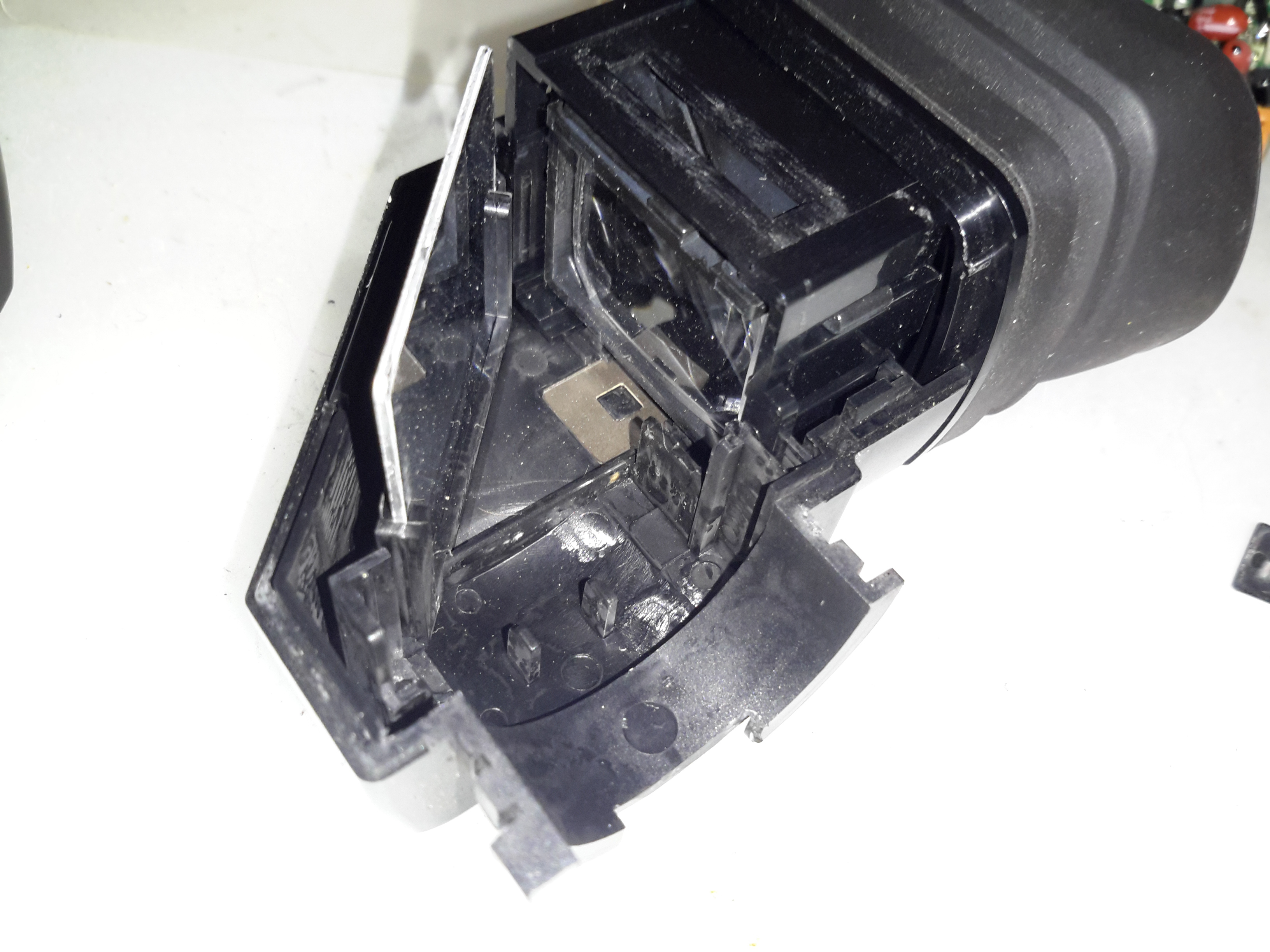
Viewfinder Assembly
As usual with these cameras, this section is the CRT based viewfinder. These units take the composite signal from the camera to display the scene. This one has many more pins than the usual viewfinder. I’ll hack a manual input into this, but I’ll leave that for another post.
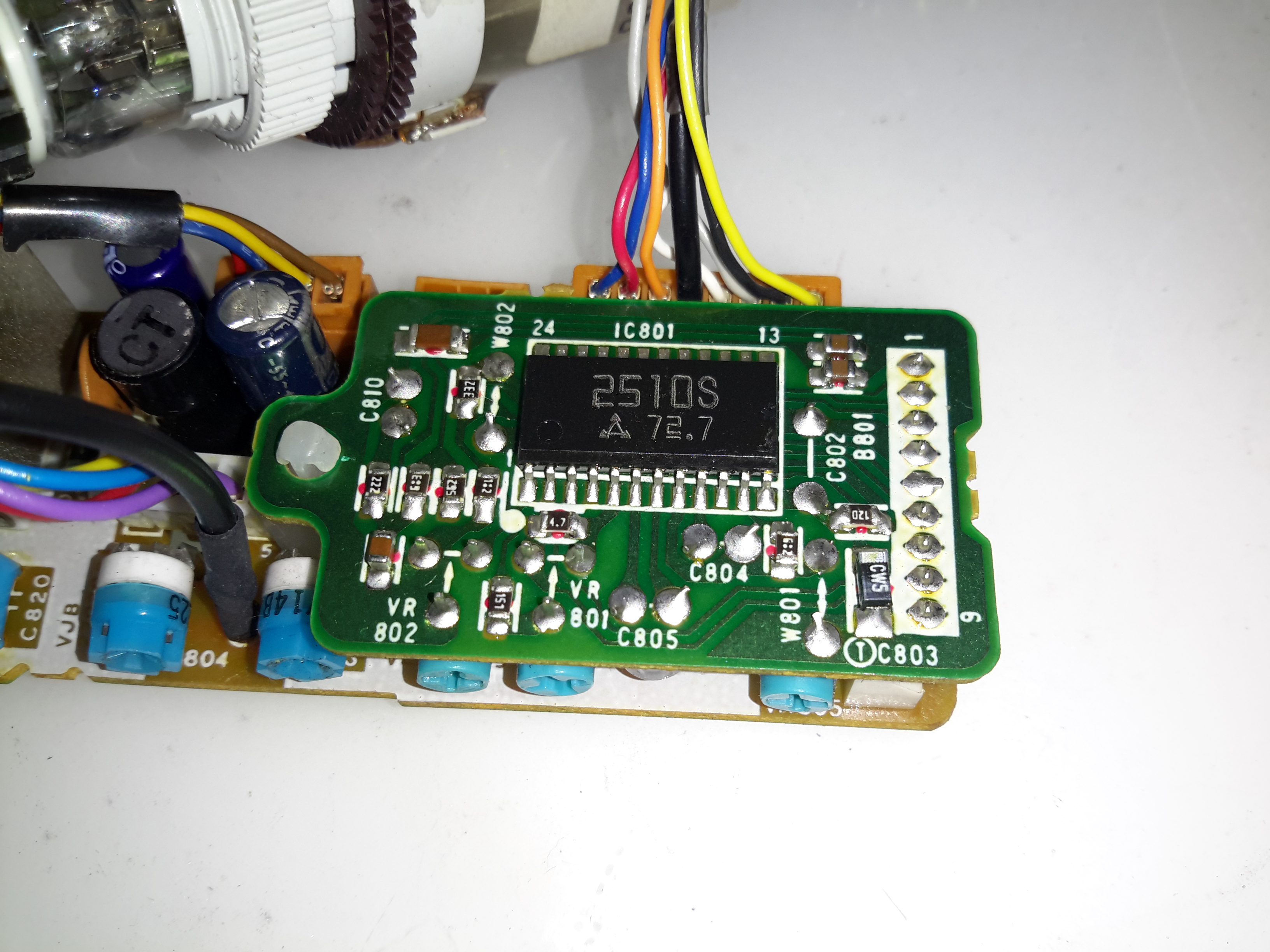
Viewfinder Circuits
Being an older camera than the ones I’ve had before, this one is on a pair of PCBs, which are both single-sided.
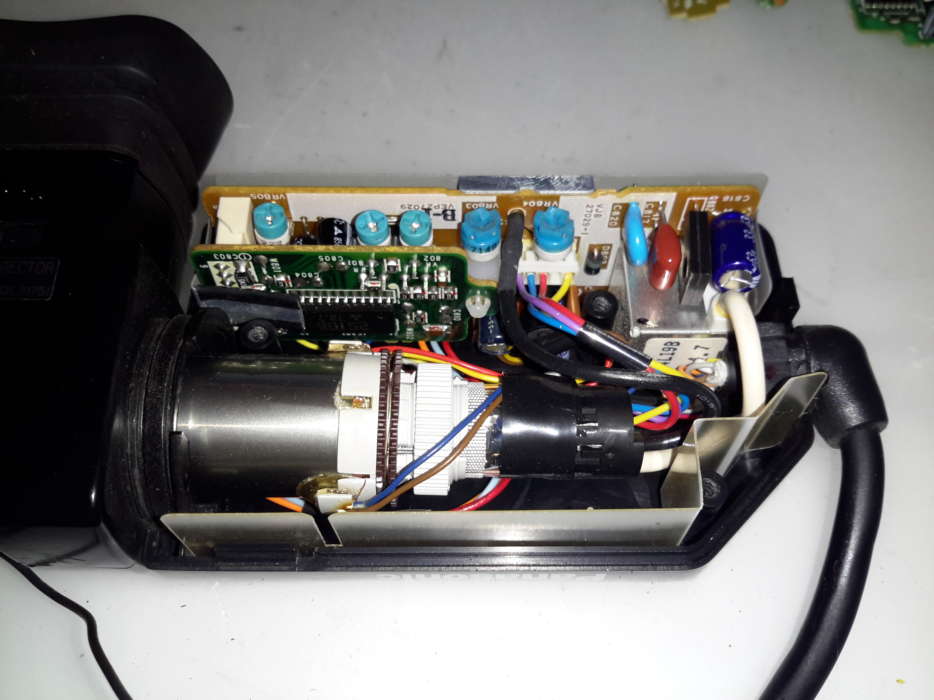
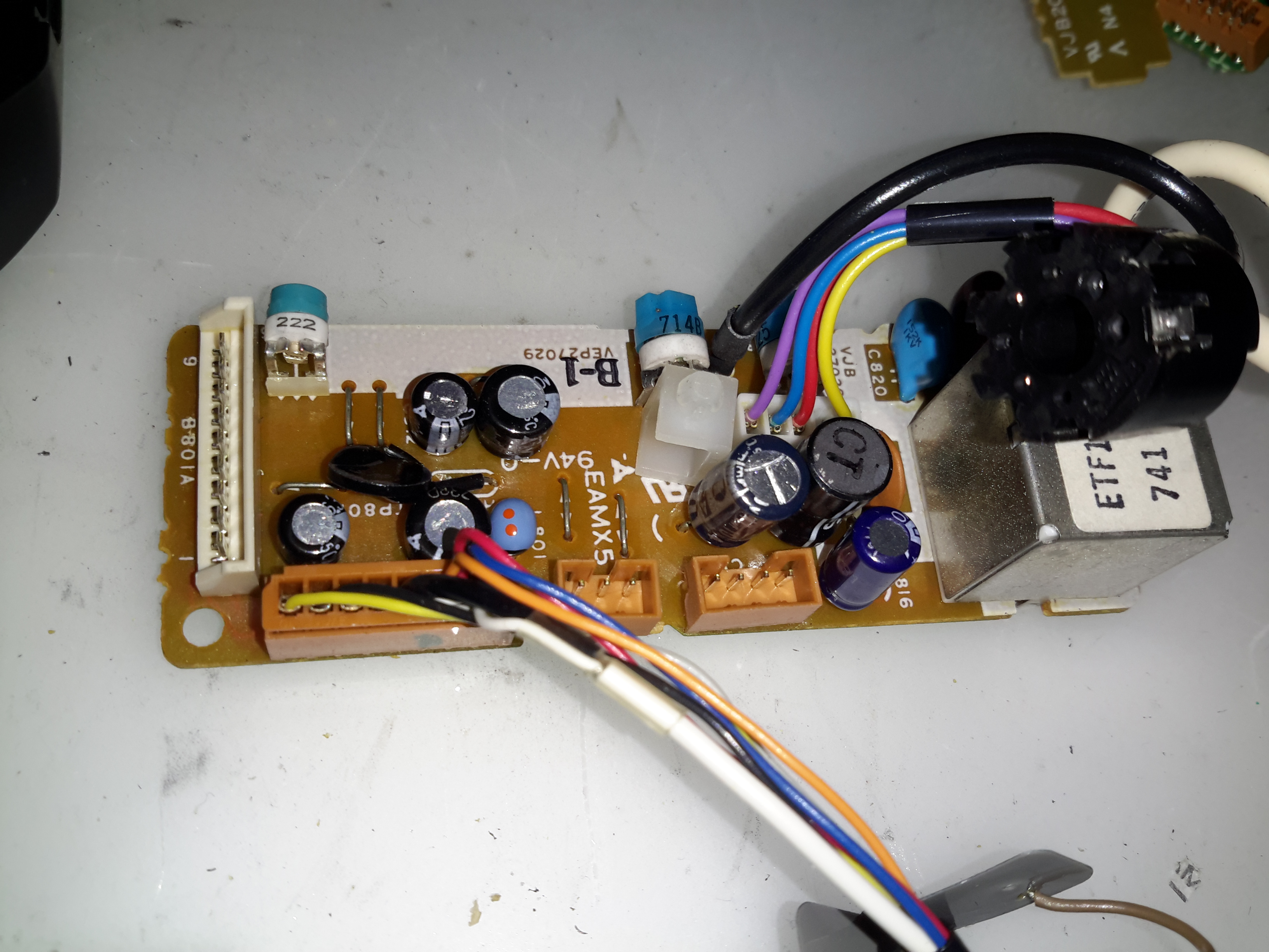
Main Viewfinder Board
The main board has all the power components for driving the CRT & some of the adjustments. The main HV flyback transformer is on the right. This part creates both the final anode voltage for the tube & the focus/grid voltages.
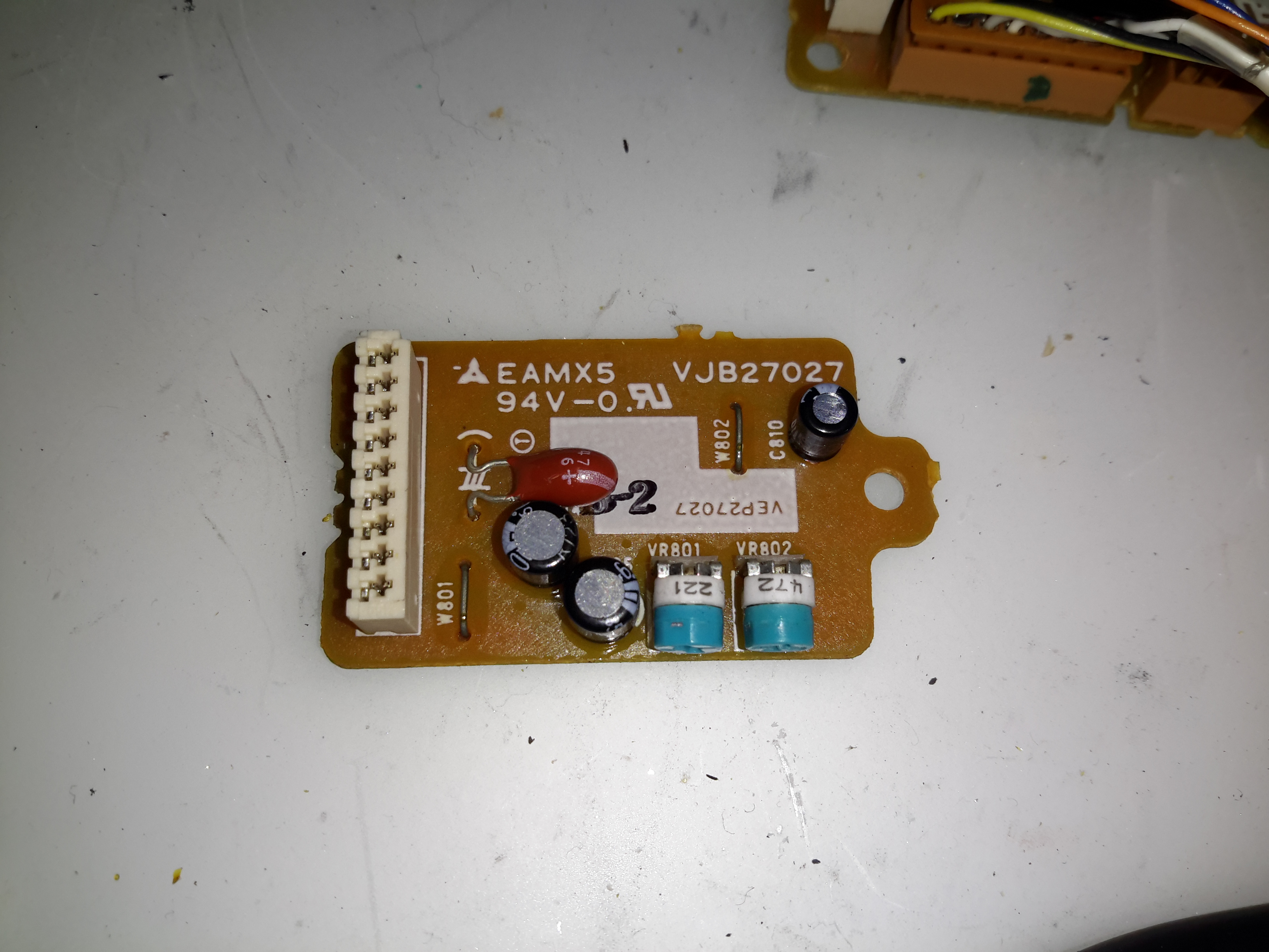
Viewfinder Control PCB Top
The viewfinder control IC is on a separate daughter board in this camera, with two more controls.
Control IC
The control IC is a Matsushita AN2510S, this has all the logic required to separate the sync pulses from the composite signal & generate an image on the CRT.
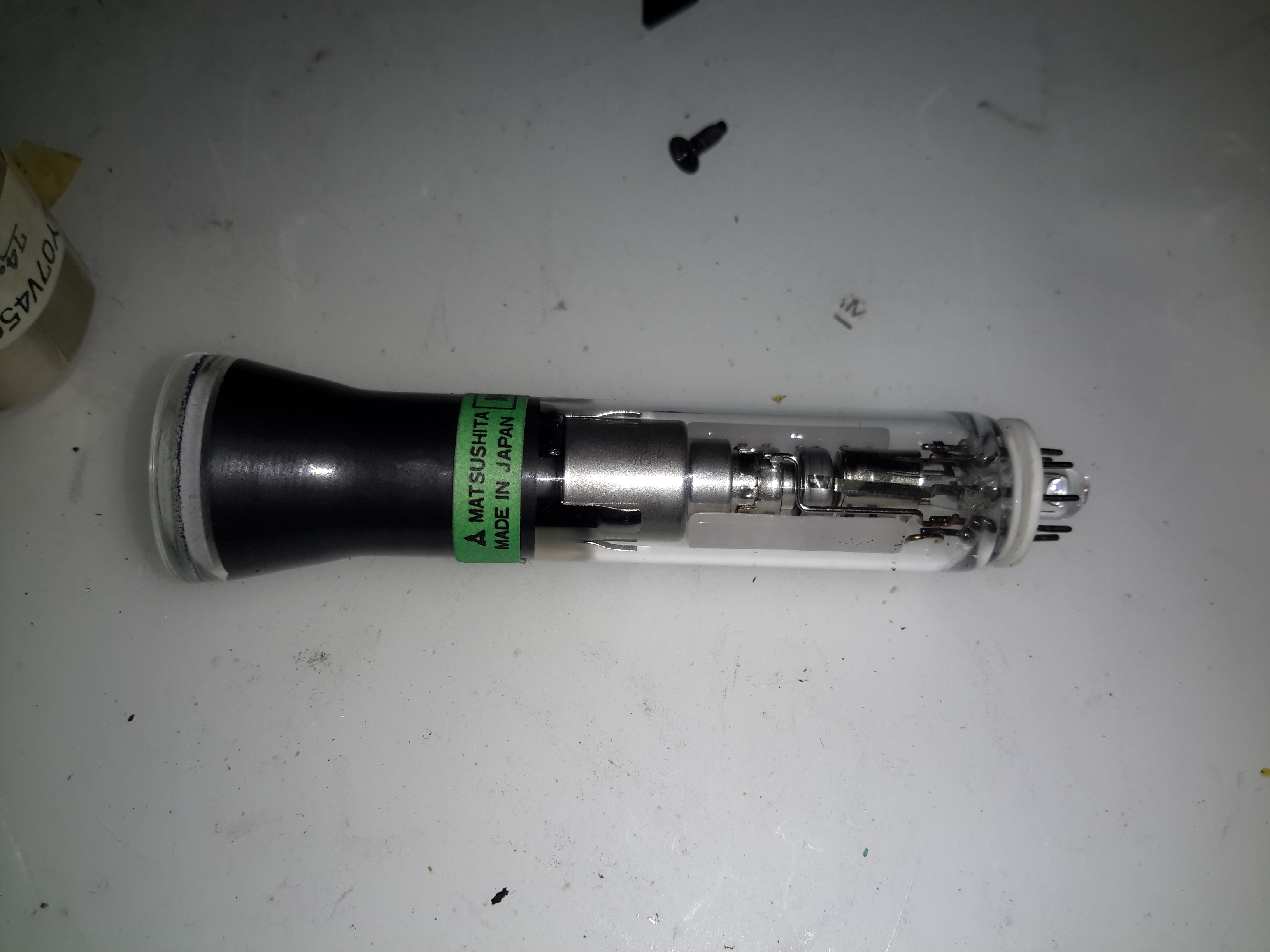
Viewfinder CRT Frame
The recording indicator LEDs are mounted in the frame of the CRT & appear above the image in the viewfinder.
Viewfinder CRT With Yoke
Here the CRT has been separated from the rest of the circuitry with just the deflection yoke still attached.
M01JPG5WB CRT
The electron gun in this viewfinder CRT is massive in comparison to the others that I have seen, and the neck of the tube is also much wider. These old tubes were very well manufactured.
Viewfinder Optics
A simple mirror & magnifying lens completes the viewfinder unit.
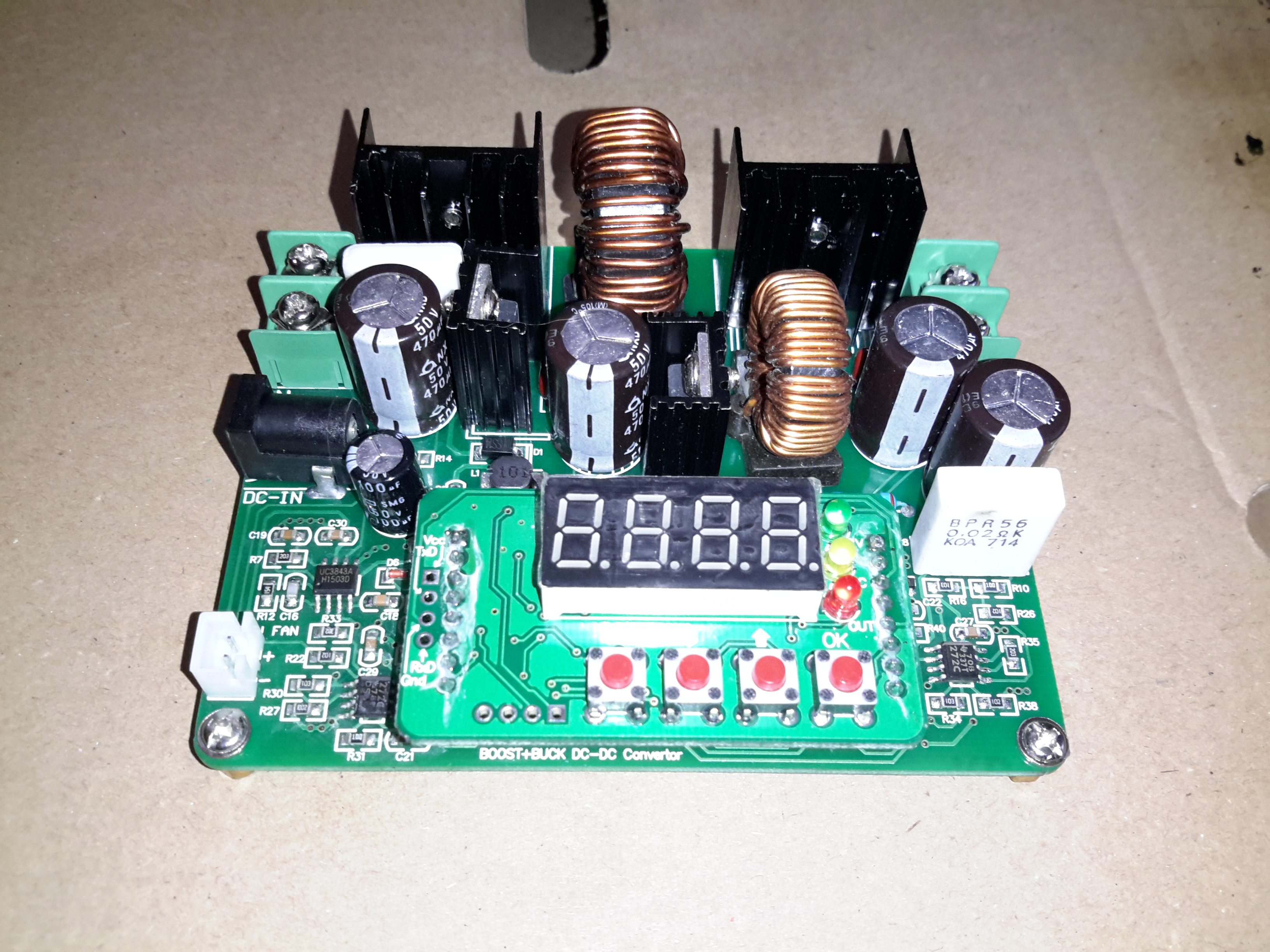
Here’s a useful buck-boost DC-DC converter from eBay, this one will do 36v DC at 6A maximum output current. Voltage & current are selected on the push buttons, when the output is enabled either the output voltage or the output current can be displayed in real time.
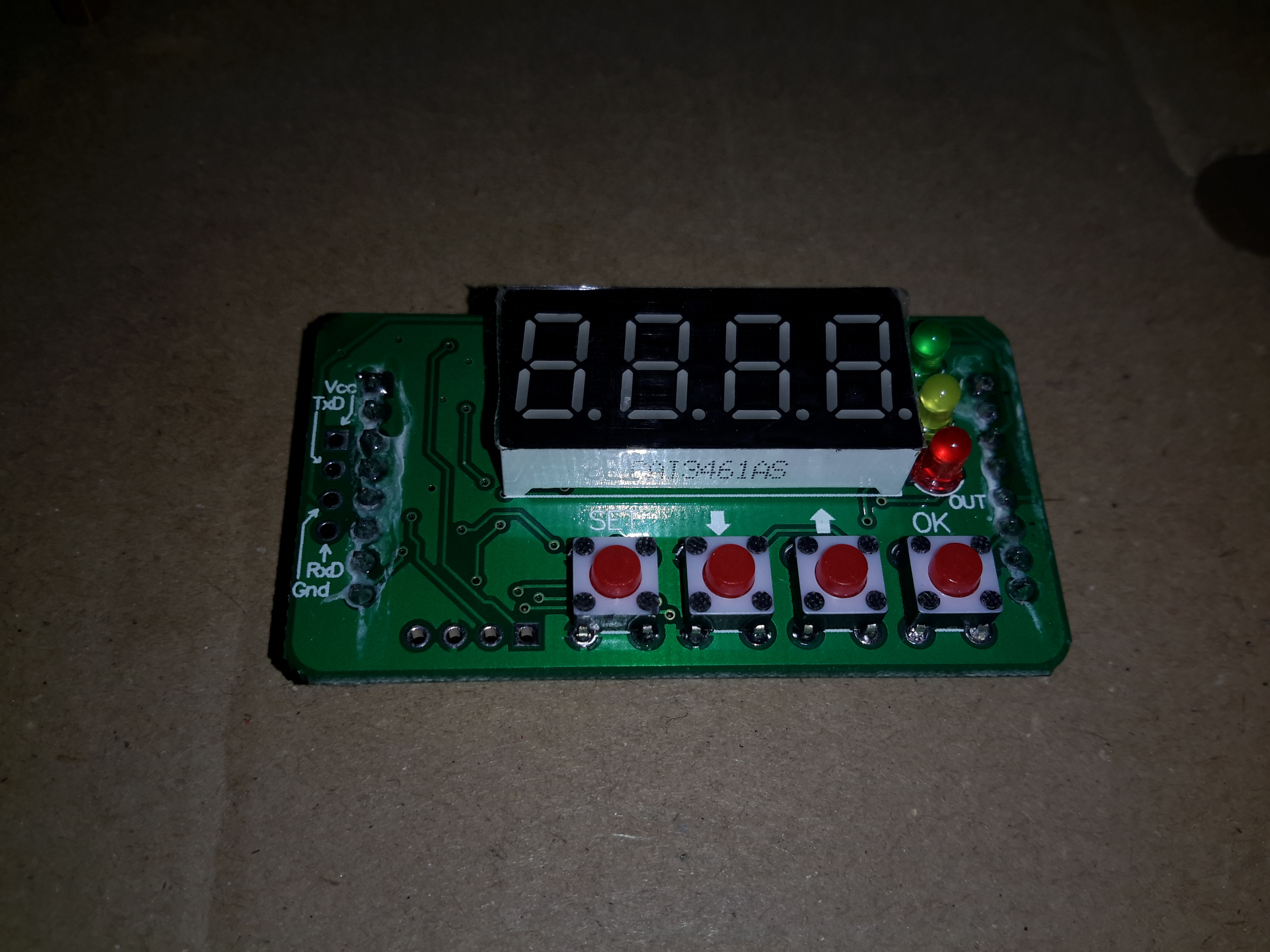
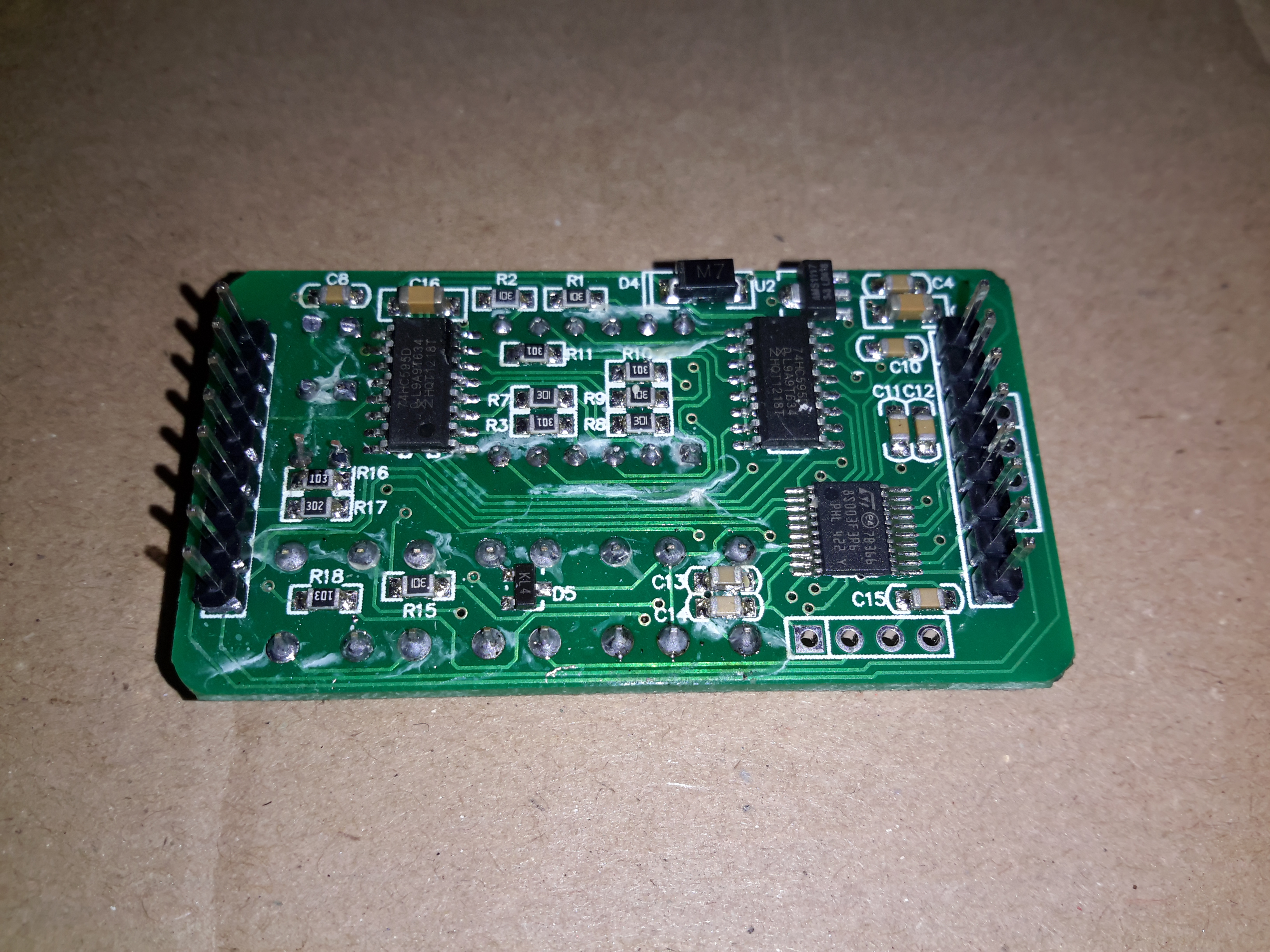
Display PCB
Here’s the display PCB, which also has the STM32 microcontroller that does all the magic. There appears to be a serial link on the left side, I’ve not yet managed to get round to hooking it into a serial adaptor to see if there’s anything useful on it.
Display Drive & Microcontroller
The bottom of the board holds the micro & the display multiplexing glue logic.
Main PCB
Not much on the mainboard apart from the large switching inductors & power devices. There’s also a SMPS PWM controller, probably being controlled from the micro.
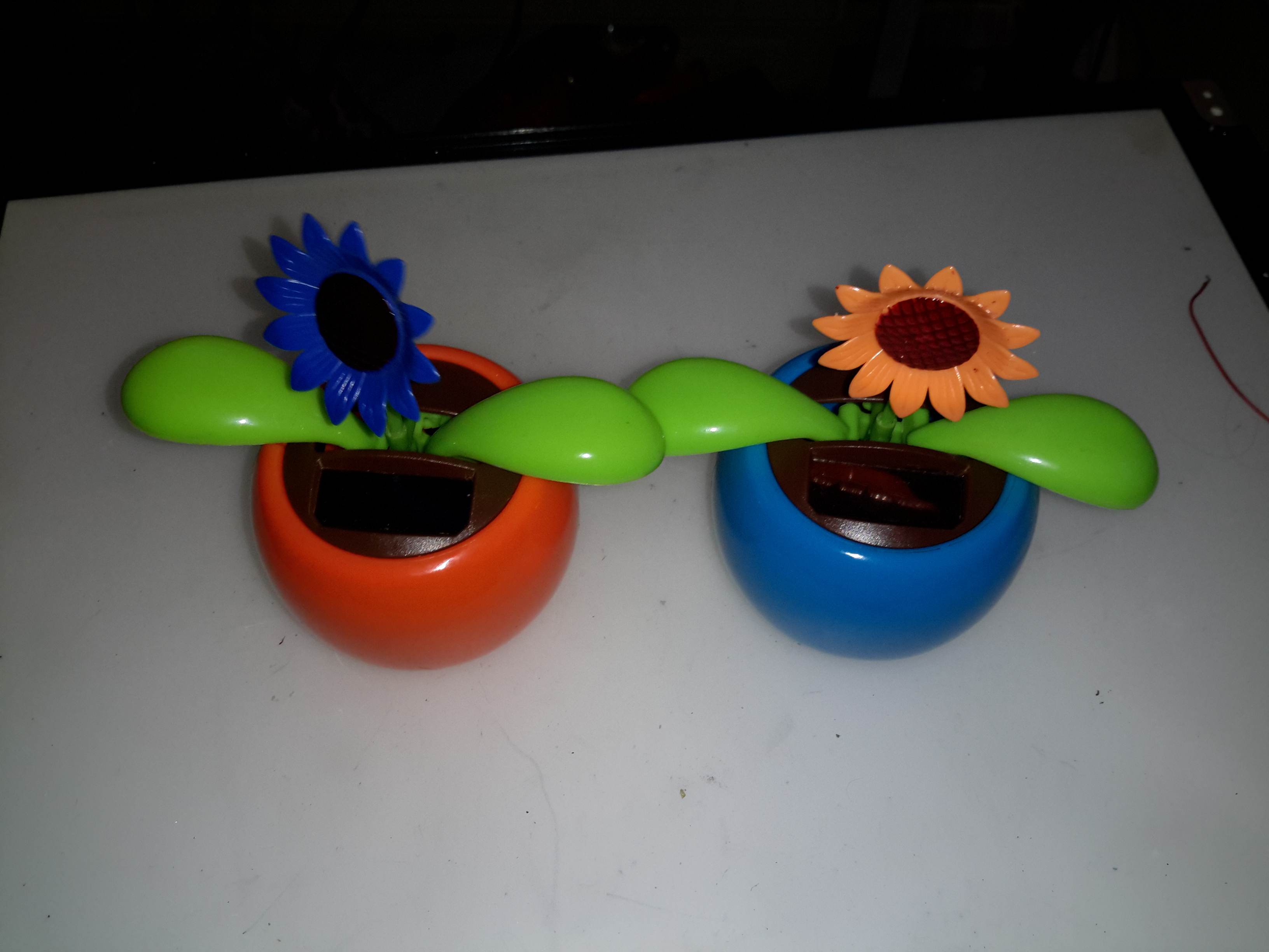
These solar flowers were being sold off at my local Tesco, a pair of them appeared thanks to my child 😉
They have a small solar panel on top, when they’re exposed to bright light, the flower & leaves move as if they’re being blown in a breeze.
Since one of them didn’t work, I figured I’d tear it down.
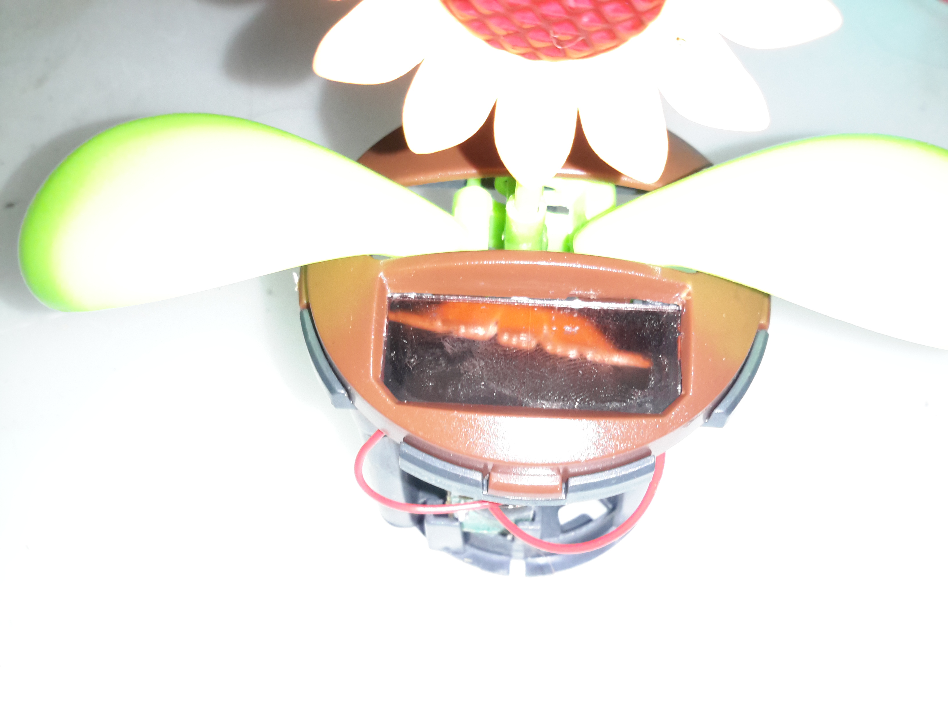
Solar Cell
The solar cell on the top is similar if not identical to that used on a cheap calculator.
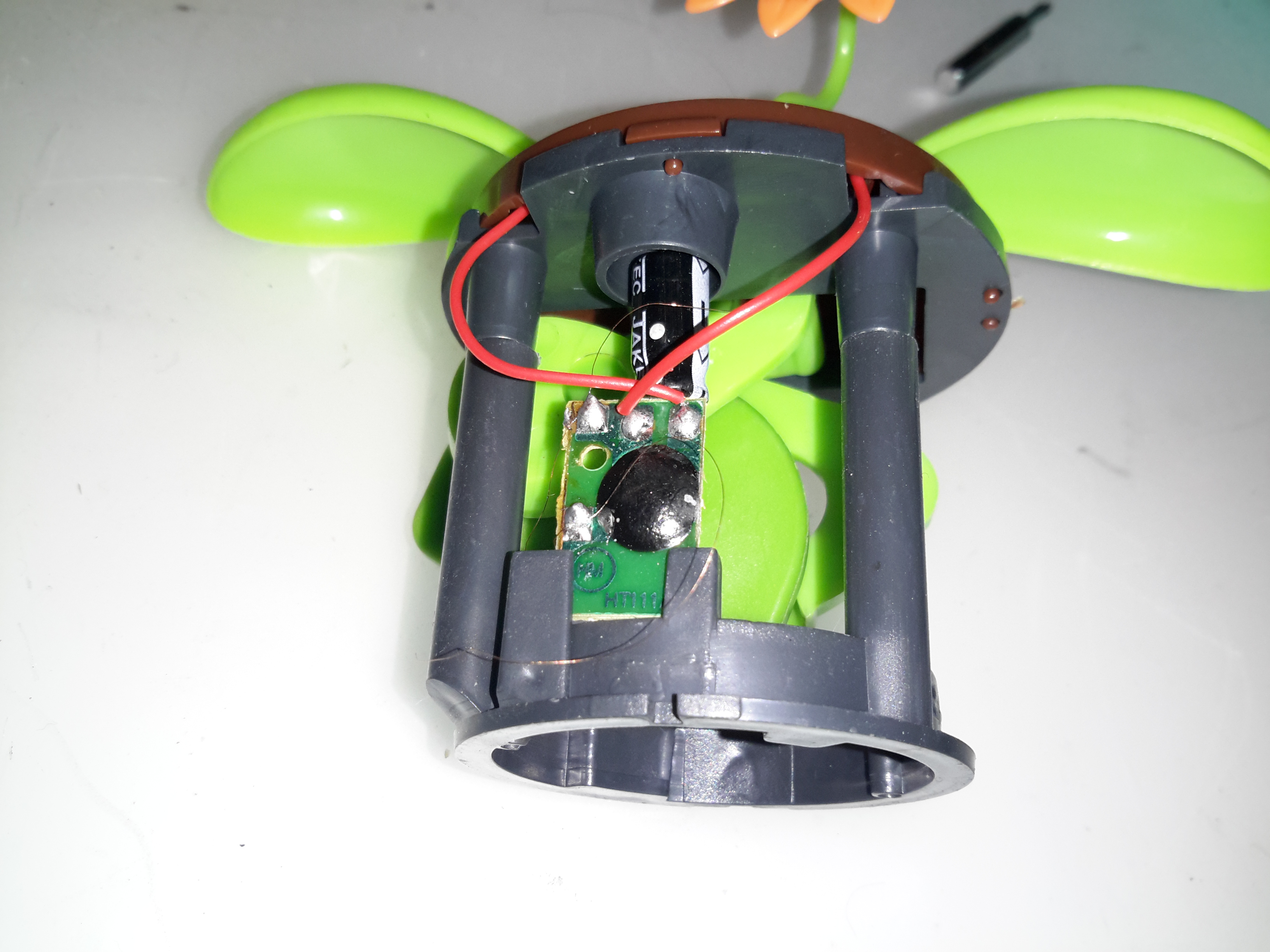
Controller
Not much to the control PCB. Just an electrolytic for smoothing the DC coming from the solar cell & a COB IC.
Electromagnet Coil
The IC drives this coil of extremely fine wire, glued to the base of the housing. Attached to the green plastic arm should be a magnet – this one has never worked as the magnet is missing. at 50p a piece, a magnet would cost me more than the whole device. So it’s the bin for this one.
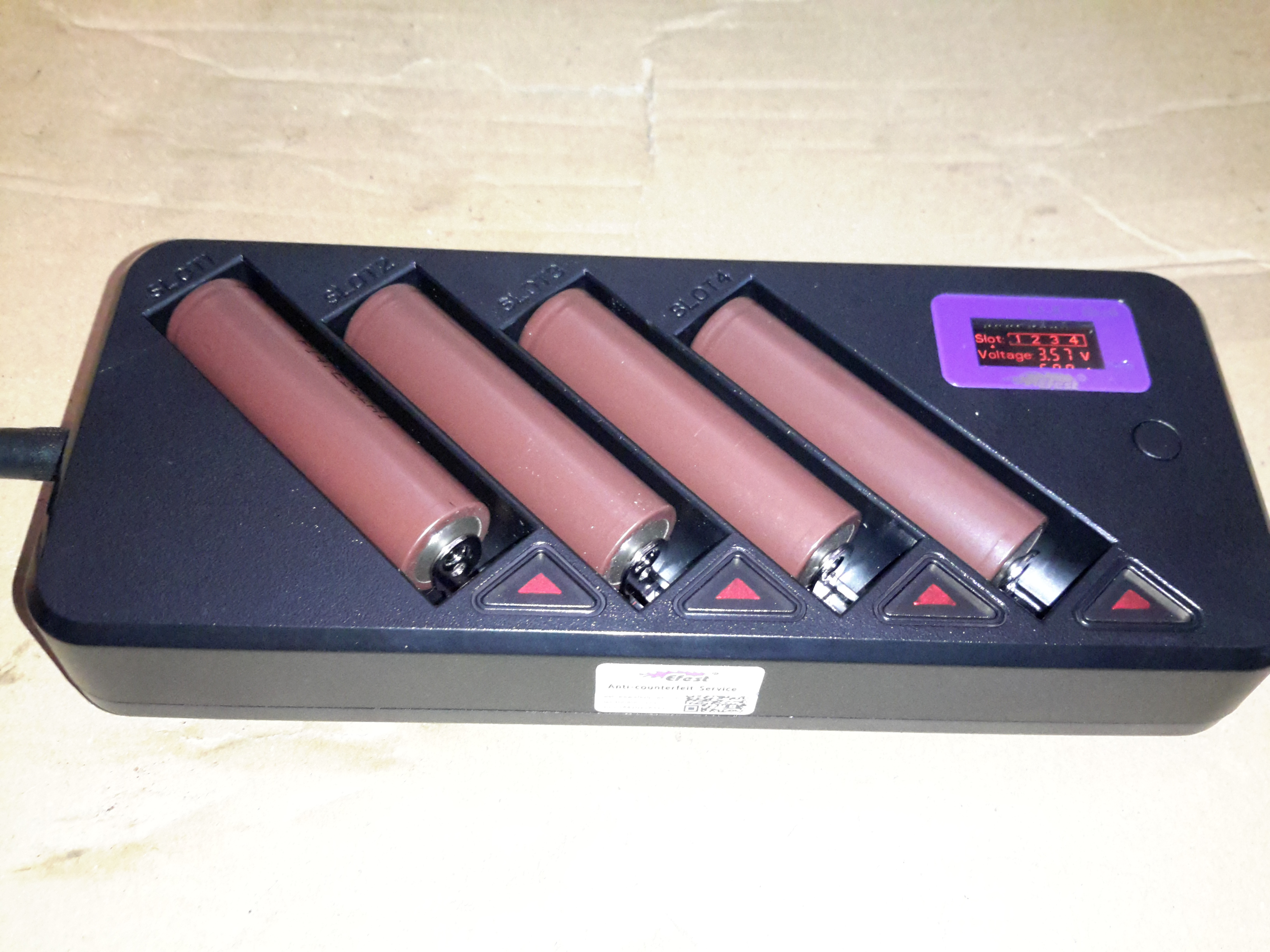
Here’s another battery charger designed for lithium chemistry cells, the BLU4. This charger doesn’t display much on it’s built in LCD, apart from basic cell voltage & charging current limits, as it has a built in Bluetooth module that will link into an Android or iOS app.
Above the charger is operating with 4 brand new cells, at a current of 500mA per cell. If only a pair of cells is being charged, the current can be increased to 1A per cell.
LCD
Not much in the way of user interface on the charger, a tiny LCD & single button for cycling through the display options.
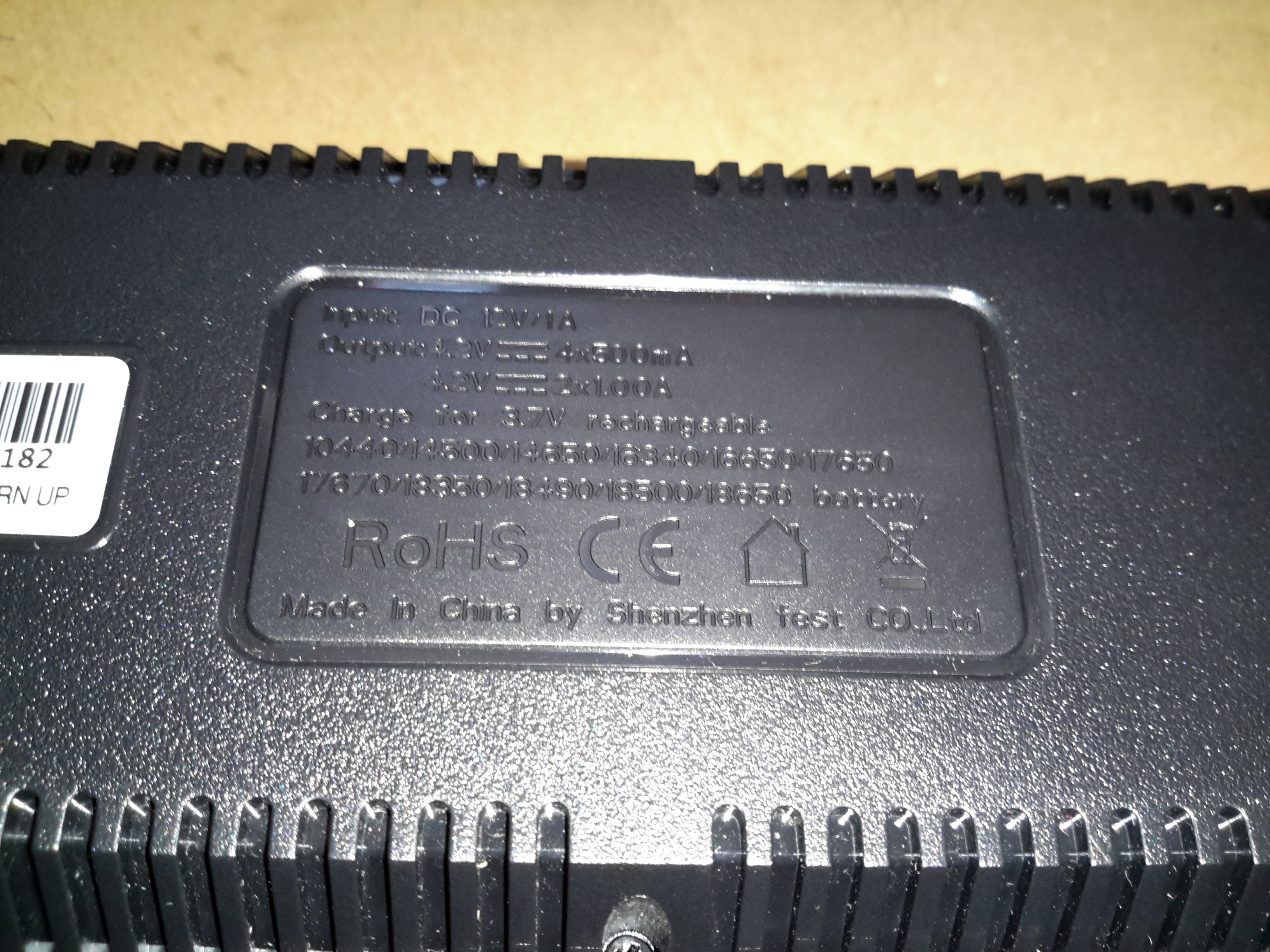
Dataplate
The usual stuff on the data plate, the charger accepts an input of 12v DC at 1A.
Bottom Cover Removed
Removing the 6 screws on the bottom of the casing allows the board to be seen. Not much on the bottom, the 4 cell negative connections can be seen, with their springs for adjusting for cell length.
MOSFETs
There’s a couple of P-Channel FETs on the bottom side for the charging circuits, along with some diodes.
Main PCB
The main PCB is easily removed after the springs are unhooked from the terminals. Most of the power circuitry is located on the top side near the power input. There are 4 DC-DC converters on board for stepping the input 12v down to the 4.2v required to charge a lithium cell.
Second Controller
Not entirely sure what this IC is in the bottom corner, as it’s completely unmarked. I’m guessing it’s a microcontroller though.
DC Input Side
The top left of the board is crammed with the DC-DC converters, all the FETs are in SO8 packages.
DC-DC Converters
One pair of DC-DC inductors is larger than the other pair, for reasons I’m unsure of.
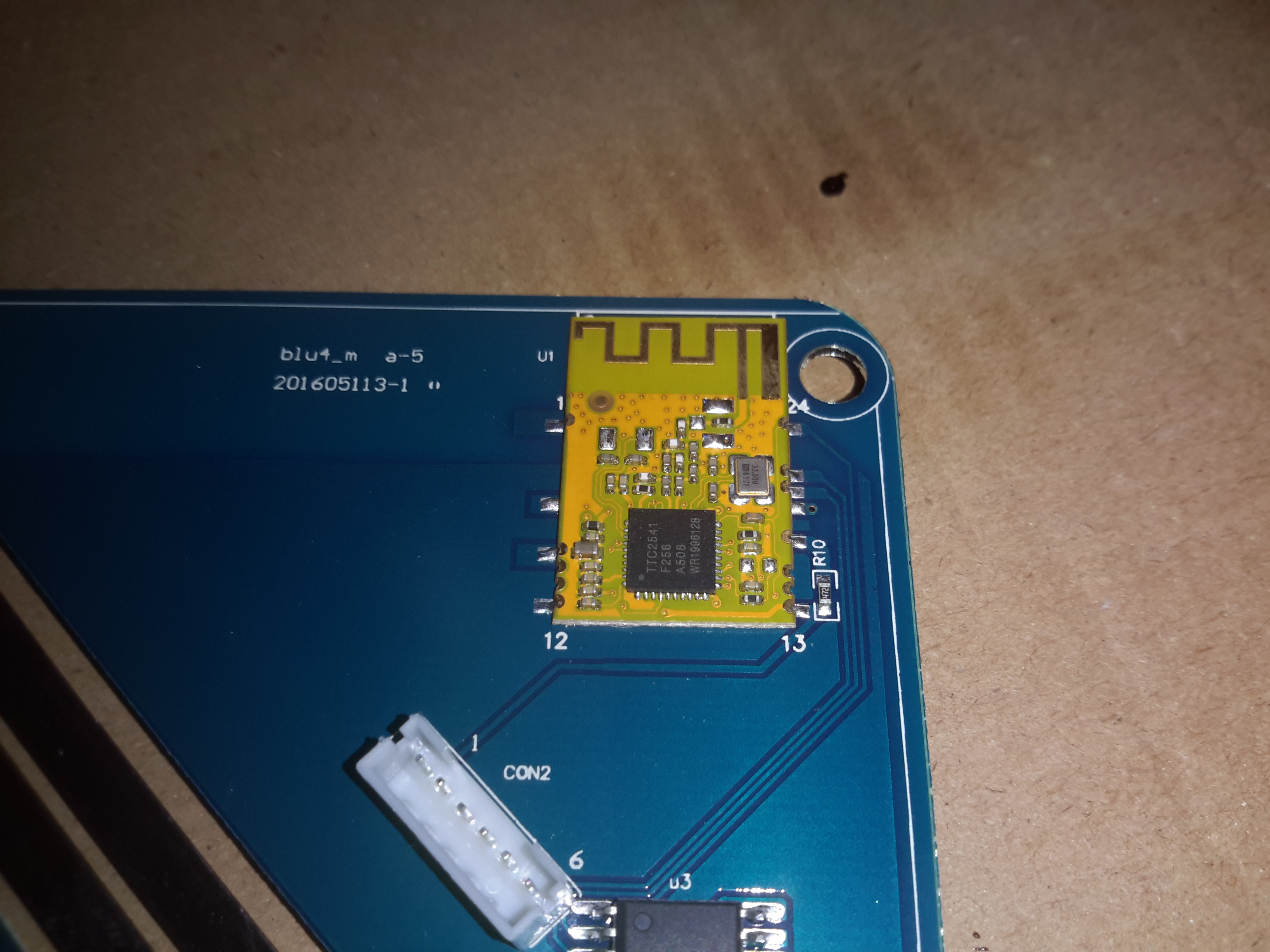
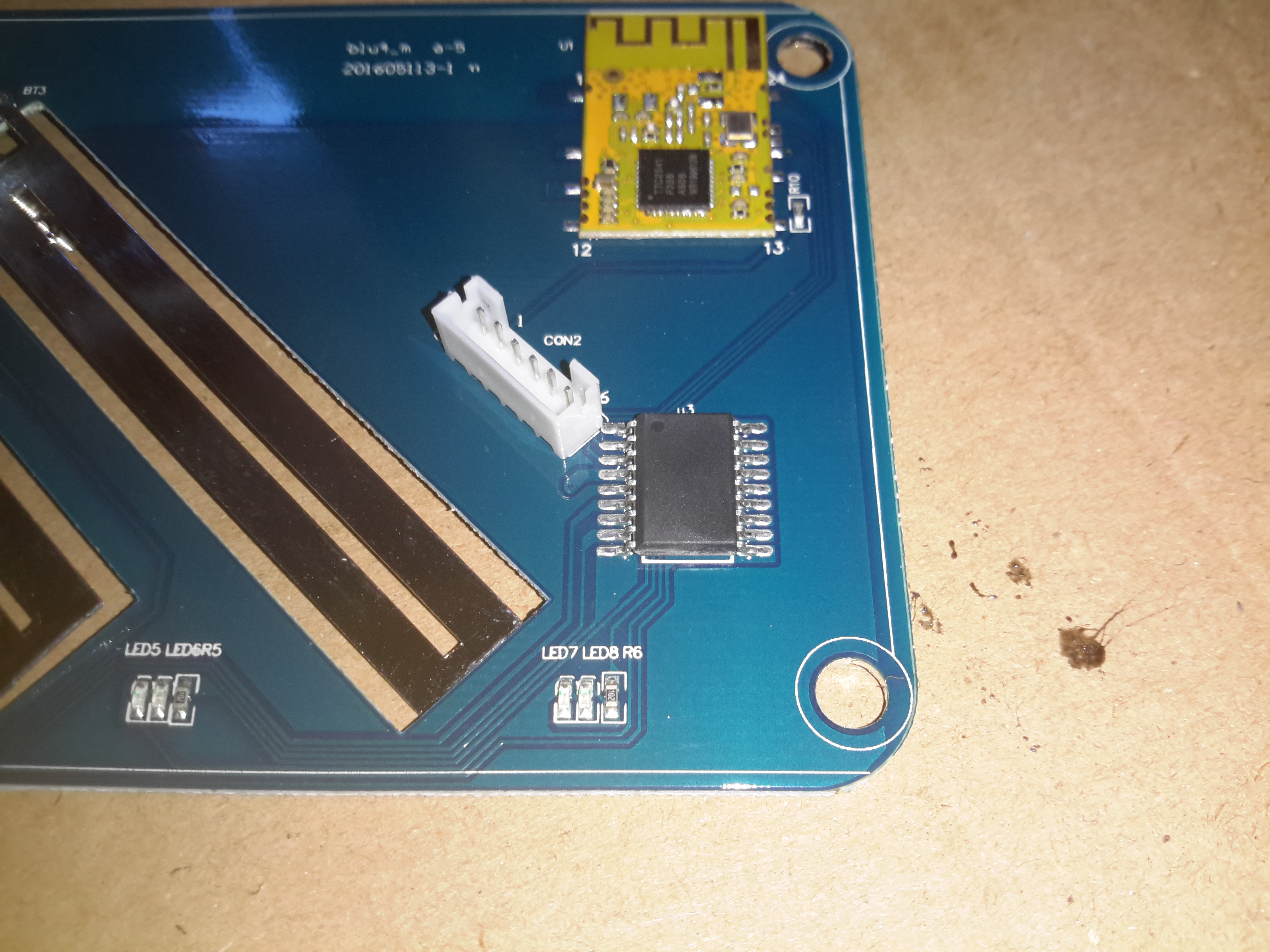
Bluetooth Module
Bluetooth connectivity is provided by this module, which is based around a TTC2541 BLE IC.
Microcontroller
Below the Bluetooth module is yet another completely unmarked IC, the direct link to the BLE interface probably means it’s another microcontroller. The Socket to the left of the IC is the connector for the front panel LCD & button.
LCD PCB
There’s not much to the LCD itself, so I won’t remove this board. The LCD controller is a COB type device, from the number of connections it most likely communicates with the micro via serial.
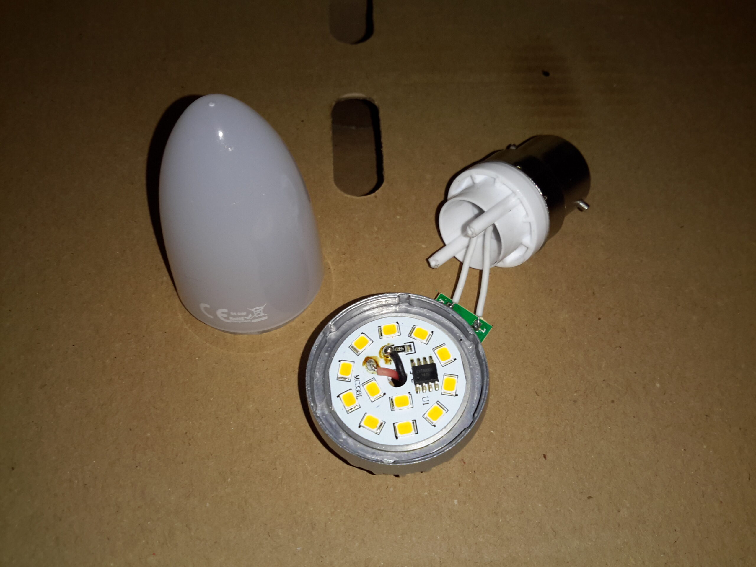
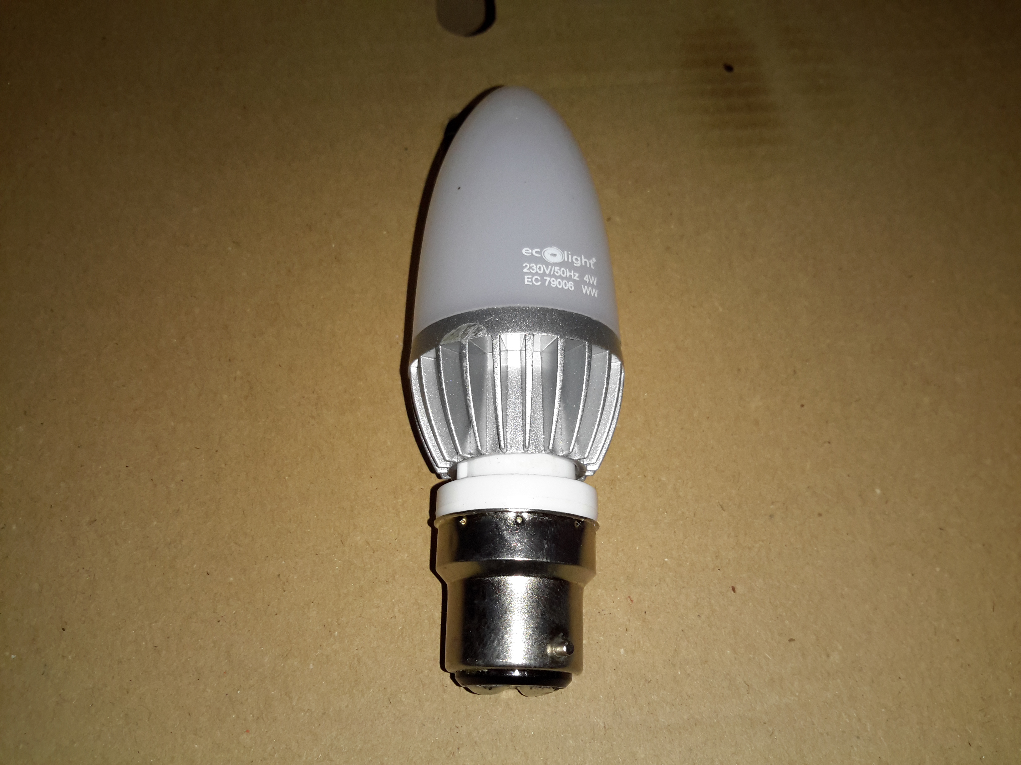
Here’s a modern LED bulb, that unfortunately decided to disassemble itself within a few minutes of being installed in a light fitting! The base plastic snapped off the main aluminium body at the screw posts!
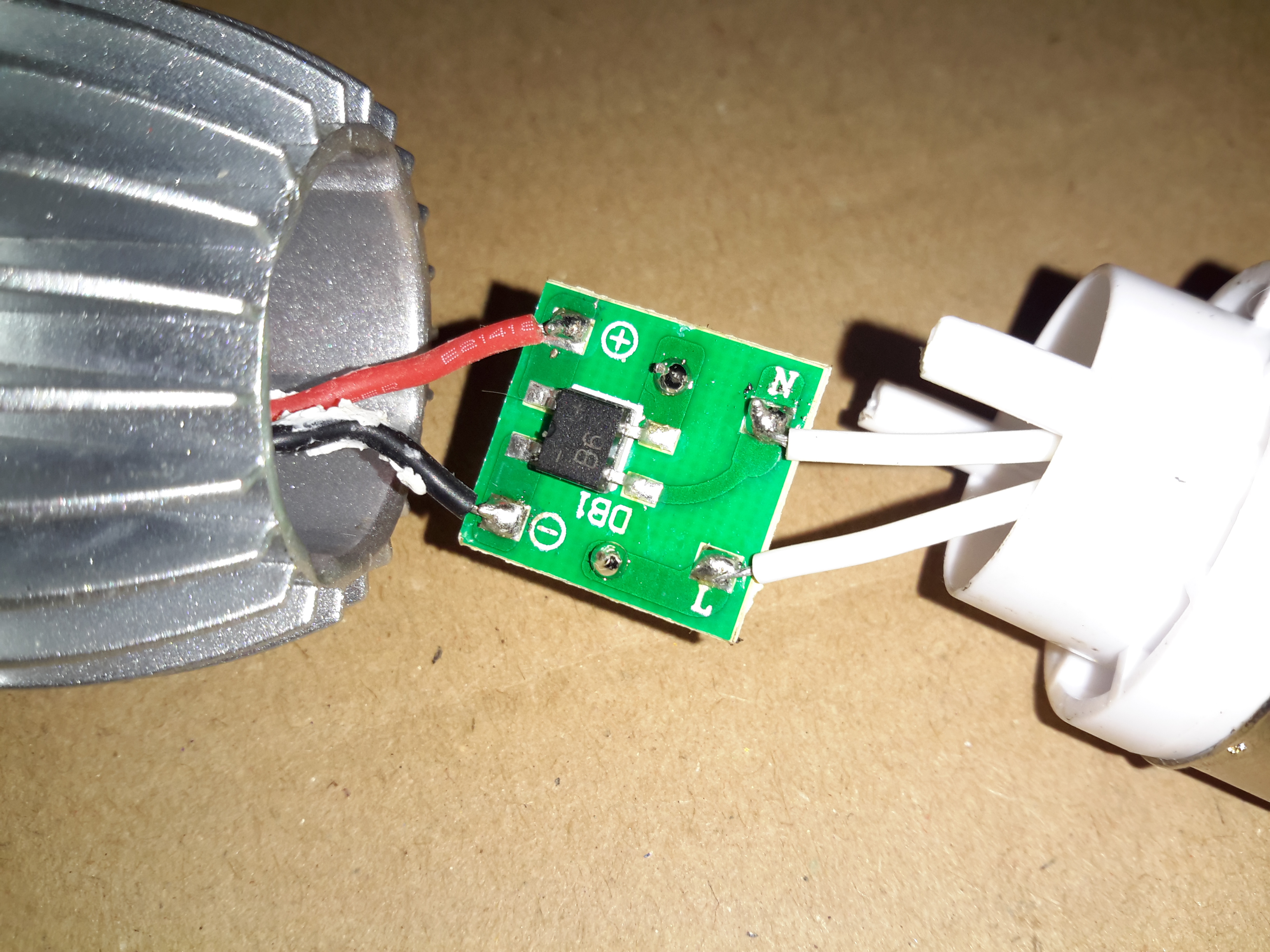
Input Rectifier
The PCB in the base holds nothing but the input components. Above is the bridge rectifier.
Fusible Resistor
The other side of the PCB has a 10Ω fusible resistor, for protection.
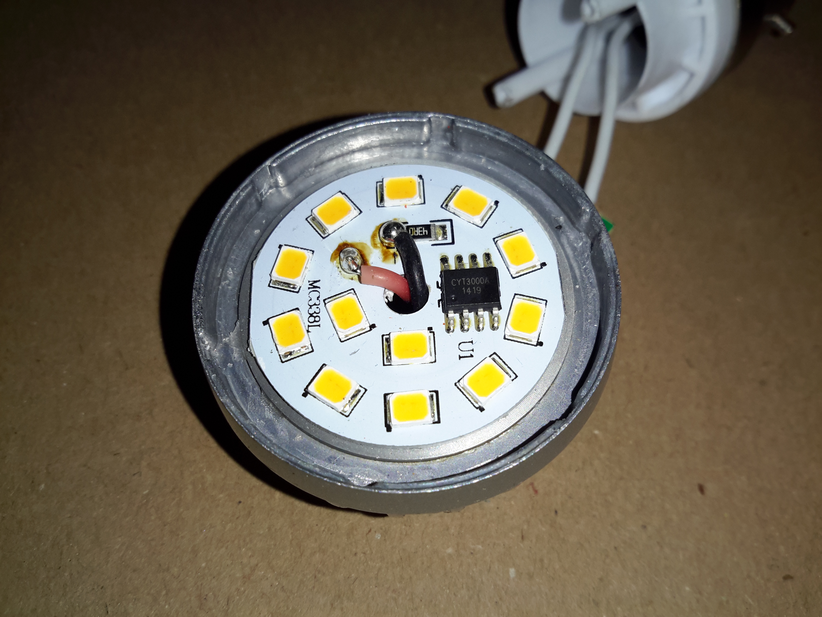
LED PCB
The LED PCB itself has the driver IC, which is a CYT3000A linear constant current IC, that runs direct from full-wave rectified mains. The single resistor sets the LED current, but there aren’t any smoothing capacitors on the DC rail, so this bulb would flicker a lot.
A helium-neon (henceforth abbreviated HeNe) laser is basically a fancy neon sign with mirrors at both ends. Well, not quite, but really not much more than this at first glance (though the design and manufacturing issues which must be dealt with to achieve the desired beam characteristics, power output, stability, and life span, are non-trivial). The gas fill is a mixture of helium and neon gas at low pressure. A pair of mirrors – one totally reflective (called the High Reflector or HR), the other partially reflective (called the Output Coupler or OC) at the wavelength of the laser’s output – complete the resonator assembly. This is called a Fabry-Perot cavity (if you want to impress your friends). The mirrors may be internal (common on small and inexpensive tubes) or external (on precision high priced lab quality lasers). Electrodes sealed into the tube allow for the passage of high voltage DC current to excite the discharge.
Note that a true laser jock will further abbreviate “HeNe laser” to simply “HeNe”, pronounced: Hee-nee. Their laser jock colleagues and friends then know this really refers to a laser! 🙂 While other types of lasers are sometimes abbreviated in an analogous manner, it is never to the same extent as the HeNe.
I still consider the HeNe laser to be the quintessential laser: An electrically excited gas between a pair of mirrors. It is also the ideal first laser for the experimenter and hobbyist. OK, well, maybe after you get over the excitement of your first laser pointer! 🙂 HeNe’s are simple in principle though complex to manufacture, the beam quality is excellent – better than anything else available at a similar price. When properly powered and reasonable precautions are taken, they are relatively safe if the power output is under 5 mW. And such a laser can be easily used for many applications. With a bare HeNe laser tube, you can even look inside while it is in operation and see what is going on. Well, OK, with just a wee bit of imagination! 🙂 This really isn’t possible with diode or solid state lasers.
I remember doing the glasswork for a 3 foot long HeNe laser (probably based on the design from: “The Amateur Scientist – Helium-Neon Laser”, Scientific American, September 1964, and reprinted in the collection: “Light and Its Uses” [5]). This included joining side tubes for the electrodes and exhaust port, fusing the electrodes themselves to the glass, preparing the main bore (capillary), and cutting the angled Brewster windows (so that external mirrors could be used) on a diamond saw. I do not know if the person building the laser ever got it to work but suspect that he gave up or went on to other projects (which probably were also never finished). And, HeNe lasers are one of the simplest type of lasers to fabricate which produce a visible continuous beam.
Some die-hards still construct their own HeNe lasers from scratch. Once all the glasswork is complete, the tube must be evacuated, baked to drive off surface impurities, backfilled with a specific mixture of helium to neon (typically around 7:1 to 10:1) at a pressure of between 2 and 5 Torr (normal atmospheric pressure is about 760 Torr – 760 mm of mercury), and sealed. The mirrors must then be painstakingly positioned and aligned. Finally, the great moment arrives and the power is applied. You also constructed your high voltage power supply from scratch, correct? With luck, the laser produces a beam and only final adjustments to the mirrors are then required to optimize beam power and stability. Or, more, likely, you are doing all of this while your vacuum pumps are chugging along and you can still play with the gas fill pressure and composition. What can go wrong? All sorts of things can go wrong! With external mirrors, the losses may be too great resulting in insufficient optical gain in the resonant cavity. The gas mixture may be incorrect or become contaminated. Seals might leak. Your power supply may not start the tube, or it may catch fire or blow up. It just may not be your day! And, the lifetime of the laser is likely to end up being only a few hours in any case unless you have access to an ultra-high vacuum pumping and bakeout facility. While getting such a contraption to work would be an extremely rewarding experience, its utility for any sort of real applications would likely be quite limited and require constant fiddling with the adjustments. Nonetheless, if you really want to be able to say you built a laser from the ground up, this is one approach to take! (However, the CO2 and N2 lasers are likely to be much easier for the first-time laser builder.)
However, for most of us, ‘building’ a HeNe laser is like ‘building’ a PC: An inexpensive HeNe tube and power supply are obtained, mounted, and wired together. Optics are added as needed. Power supplies may be home-built as an interesting project but few have the desire, facilities, patience, and determination to construct the actual HeNe tube itself.
The most common internal mirror HeNe laser tubes are between 4.5″ and 14″ (125 mm to 350 mm) in overall length and 3/4″ to 1-1/2″ (19 mm to 37.5 mm) in diameter generating optical power from 0.5 mW to 5 mW. They require no maintenance and no adjustments of any kind during their long lifetime (20,000 hours typical). Both new and surplus tubes of this type – either bare or as part of complete laser heads – are readily available. Slightly smaller tubes (less than 0.5 mW) and much larger tubes (up to approximately 35 mW) are structurally similar (except for size) to these but are not as common.
Much larger HeNe tubes with internal or external mirrors or one of each (more than a *meter* in length!) and capable of generating up to 250 mW of optical power have been available and may turn up on the surplus market as well (but most of these are quite dead by now). The most famous of these (as lasers go) is probably the Spectra-Physics model 125A whose laser head is over 6 feet in length. It was only rated 50 mW (633 nm), but new samples under optimal conditions may have produced more than 200 mW. Even more powerful ones have been built as research projects. I’ve seen photos of a Hughes HeNe laser with a head around 8 feet in length that required a 6 foot rack-mount enclosure for the exciter.
Monster Vintage Hughes HeNe Laser System
Its output power is unknown, but probably less than that of the SP-125A. The largest single transverse mode (SM, with a TEM00 beam profile) HeNe lasers in current production by a well known manufacturer like Melles Griot are rated at about 35 mW minimum over an expected lifetime of 20,000 hours or more, though new samples may exceed 50 mW. However, HeNe lasers rated up to at least 70 mW SM and 100 mW MM are available. Manufacturers include: CDHC-Optics (China), Spectral Laser (Italy), and PLASMA, JSC (Russia). However, the lifetime over which these specifications apply is not known and may be much shorter.
Highly specialized configurations, such as a triple XYZ axis triangular cavity HeNe laser in a solid glass block for an optical ring laser gyro, also exist but are much much less common. Most HeNe lasers operate CW (Continuous Wave) producing a steady beam at a fixed output power unless the power is switched on and off or modulated (or someone sticks their finger in the beam and blocks it!). (At least they are supposed to when in good operating condition!) However, there are some mode-locked HeNe lasers that output a series of short pulses at a high repetition rate. And, in principle, it is possible to force a HeNe laser with at least one external mirror to “cavity dump” a high power pulse (perhaps 100 times the CW power) a couple of nanoseconds long by diverting the internal beam path with an ultra high speed acousto-optic deflector. But, for the most part, such systems aren’t generally useful for very much outside some esoteric research areas and in any case, you probably won’t find any of these at a local flea market or swap meet, though eBay can’t be ruled out! 🙂
Nearly all HeNe lasers output a single wavelength and it is most often red at 632.8 nm. (This color beam actually appears somewhat orange-red especially compared to many laser pointers using diode lasers at wavelengths between 650 and 670 nm). However, green (543.5 nm), yellow (594.1 nm), orange (604.6 and 611.9 nm), and even IR (1,152, 1.523, and 3,921 nm) HeNe lasers are available. There are a few high performance HeNe lasers that are tunable and very expensive. And, occasionally one comes across laser tubes that output two or more wavelengths simultaneously. Although some tubes are designed this way, it is more likely to be a ‘defect’ resulting from a combination of high gain and insufficiently narrow band optics. Such tubes tend to be unstable with the relative power varying among the multiple wavelengths more or less at random.
Note that the single wavelength described above usually consists of more than one longitudinal mode or lasing line (more on this later). However, some HeNe lasers are designed to produce a highly stable single optical frequency or two closely spaced optical frequencies. These are used in scientific research and metrology (measurement) applications, described in more detail below.
Current major HeNe laser manufacturers include Melles-Griot, JDS Uniphase, and LASOS. This is far fewer than there were only a few years ago. So, you may also find lasers from companies like Aerotech, Hughes, Siemens, and Spectra-Physics that have since gotten out of the HeNe laser business or have been bought out, merged, or changed names. For example, the HeNe laser divisions of Aerotech and Hughes were acquired by Melles Griot; Sieman’s HeNe laser product line is now part of LASOS; and Spectra-Physics which was probably the largest producer of HeNe lasers from the very beginning gradually eliminated all HeNe lasers from its product line over the last few years. HeNe tubes, laser heads, and complete lasers from any of these manufacturers are generally of very high quality and reliability.
HeNe lasers have been found in all kinds of equipment including:
Consumer: Supermarket checkout UPC and other barcode scanners. early laser printers, early LaserDisc players.
Advertising/entertainment: Holography, small laser shows.
Measurement: Optical surveying, interferometric metrology and velocimetry, other non-contact measurement and monitoring, ring laser gyro.
Construction: Laser level, tunnel boring, alignment of saw mill wood cutting, general surveying.
Industrial: Automotive and other alignment; parts detection, counting, and positioning; particle counting.
Biotechnology: Blood cell analysis (cytometry), laser induced fluorescence of everything from whole cells to single DNA bases, laser tweezers, confocal microscopy, Raman spectroscopy, anesthesia and other gas analysis.
Medical/surgical: Patient positioning systems for diagnostic and treatment machines, alignment of high power CO2 and YAG treatment lasers and pointing beams.
Nowadays, many of these applications are likely to use the much more compact lower (drive) power solid state diode laser. (You can tell if you local ACME supermarket uses a HeNe laser in its checkout scanners by the color of the light – the 632.8 nm wavelength beam from a HeNe laser is noticeably more orange than the 660 or 670 nm deep red from a typical diode laser type.)
Melles Griot (now part of IDEX Optics and Photonics Marketplace. Catalogs used to include several pages describing HeNe laser applications. I know this was present in the 1998 catalog but has since disappeared and I don’t think it is on their Web site.
Since a 5 mW laser pointer complete with batteries can conveniently fit on a keychain and generate the same beam power as an AC line operated HeNe laser almost half a meter long, why bother with a HeNe laser at all? There are several reasons:
For many applications including holography and interferometry, the high quality stable beam of a HeNe laser is unmatched (at least at reasonable cost, perhaps at all) by laser diodes (though this is apparently changing at least for some diode lasers. See the section: Holography Using Cheap Diode Lasers. In particular, the coherence length and monochromicity of even a cheap HeNe laser are excellent and the beam profile is circular and nearly ideal Gaussian TEM00 so that simple spherical optics can be used for beam manipulation. Bare edge emitting laser diodes (the only visible type currently available) on the other hand always produce a wedge shaped beam and have some amount of astigmatism. Correcting this to the equivalent quality of a HeNe laser is difficult and expensive.
As noted in the chapter: Diode Lasers, it is all too easy to ruin them in the blink of an eye (actually, the time it takes light to travel a few feet). It would not take very long to get frustrated burning out $50 diodes. So, the HeNe laser tube may be a better way to get started. They are harder to damage through carelessness or design errors. Just don’t get the polarity reversed or exceed the tube’s rated current for too long – or drop them on the floor! And, take care around the high voltage!
Laser diode modules at a wavelength of 635 nm (close to the 632.8 nm wavelength of red HeNe lasers) may still be somewhat more expensive than surplus HeNe tubes with power supplies. However, with the increasing popularity of DVD players and DVDROM drives, this situation probably won’t last long.
However, the market for new HeNe lasers is still in the 100,000 or more units per year. What can you say? If you need a stable, round, astigmatism-free, long lived, visible 1 to 10 mW beam for under $500 (new, remember!), the HeNe laser is still the only choice.
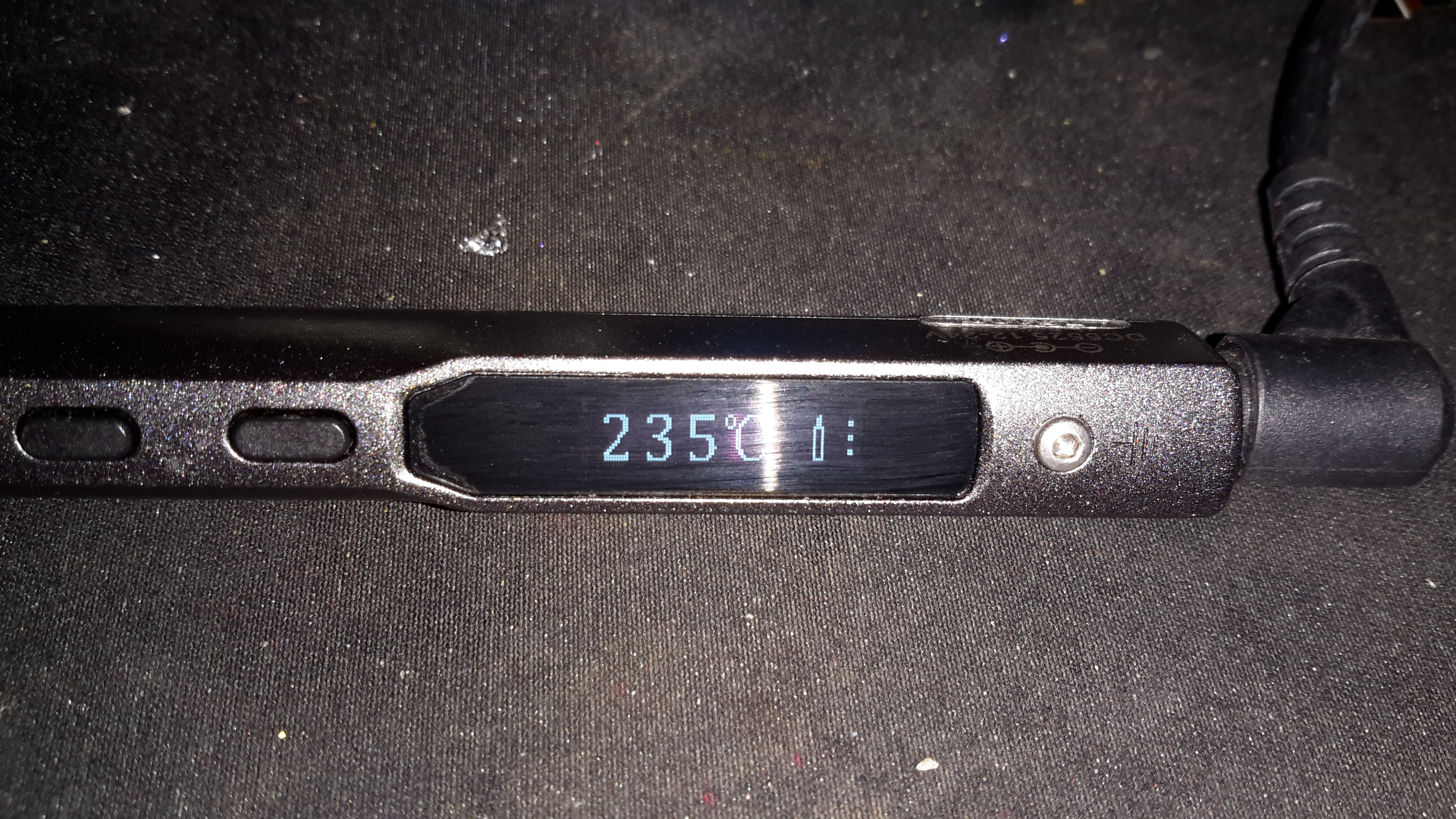
When I ordered the tiny USB soldering iron, I decided a proper iron upgrade would be a good idea. Looking around for something that didn’t require AC mains power turned up the TS100, a Chinese design, that unusually is actually very good! Above is the handle itself, with it’s small OLED display & two operation buttons.
This iron is controlled by a STM32 ARM microcontroller, the firmware & schematics are completely open-source.
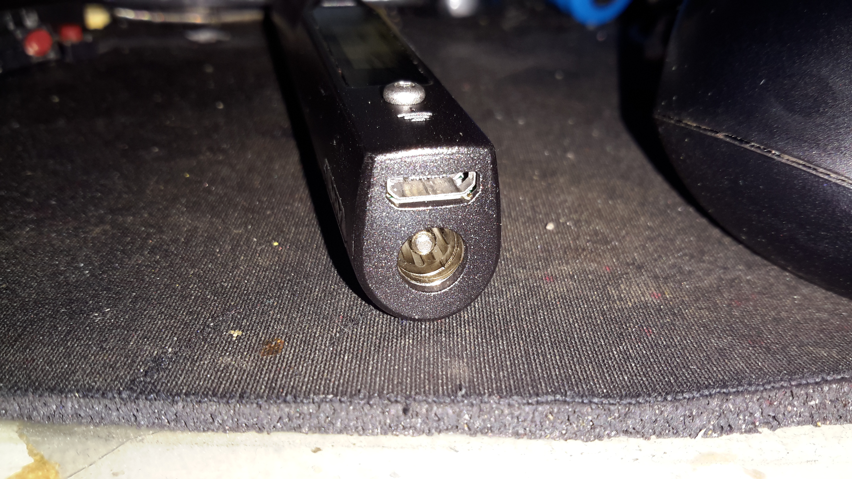
DC Input Jack / USB Port
The bottom end of the iron has the main DC input jack, designed with laptop chargers in mind (DC input range from 10v-24v). Above that is the micro USB port for programming.
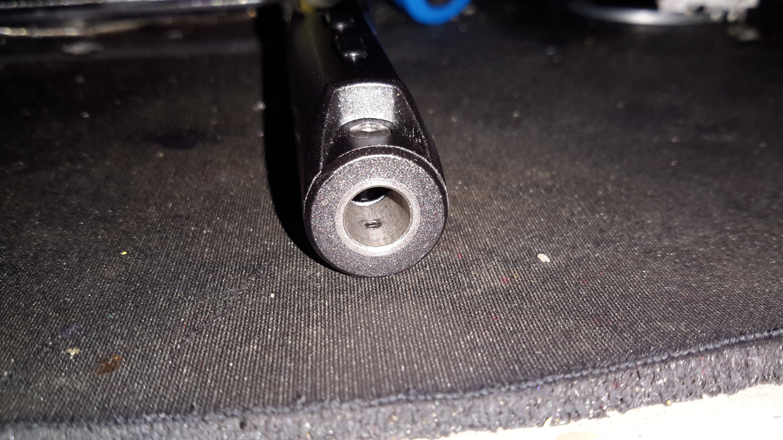
Heating Element Socket
The iron tips slot into the other end, many different tip types & shapes are available. The one supplied was the simple conical tip.
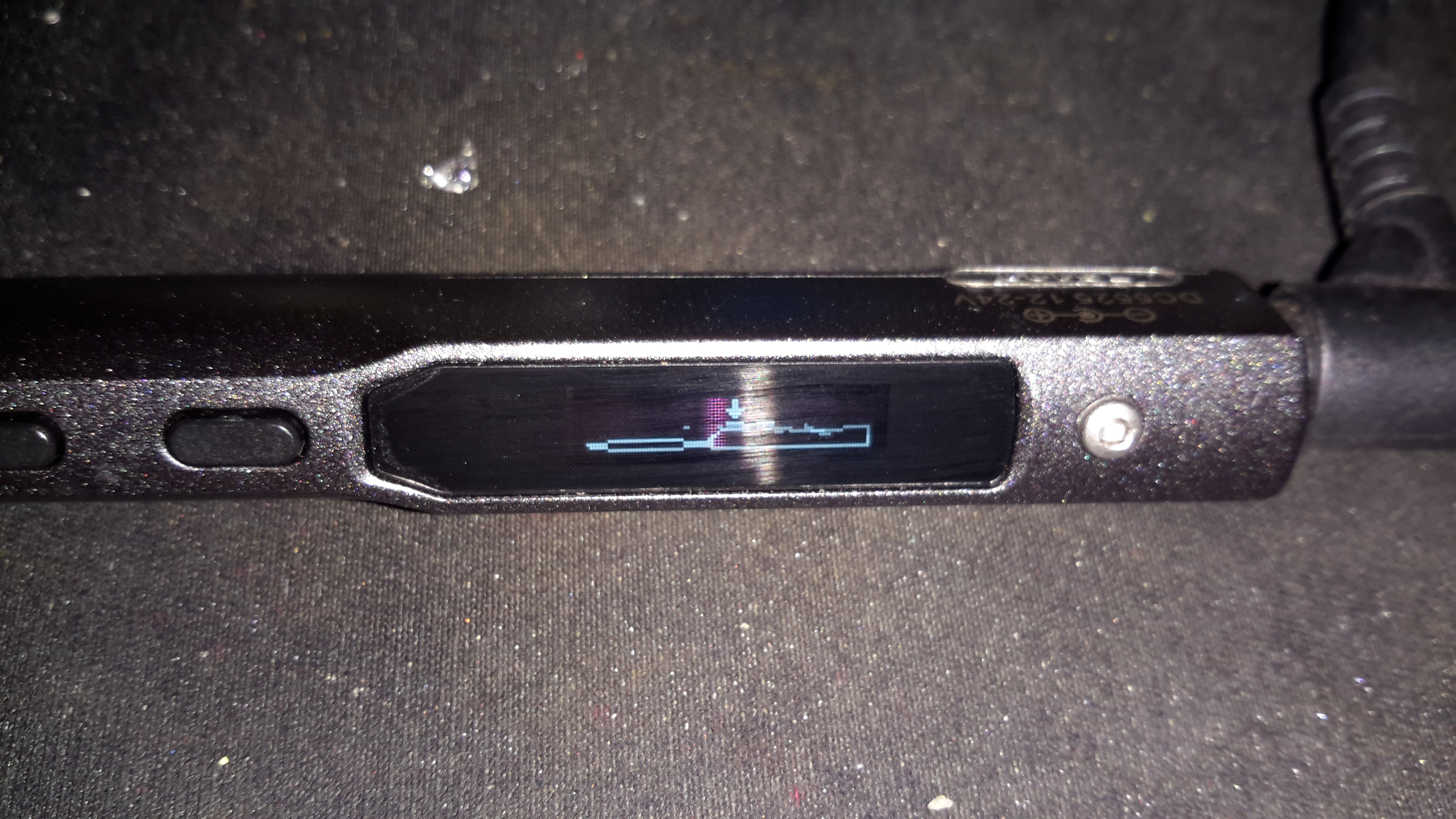
Standby Screen
Plugging the iron into some power gets a standby screen – it doesn’t just start heating immediately, for safety.
Heating
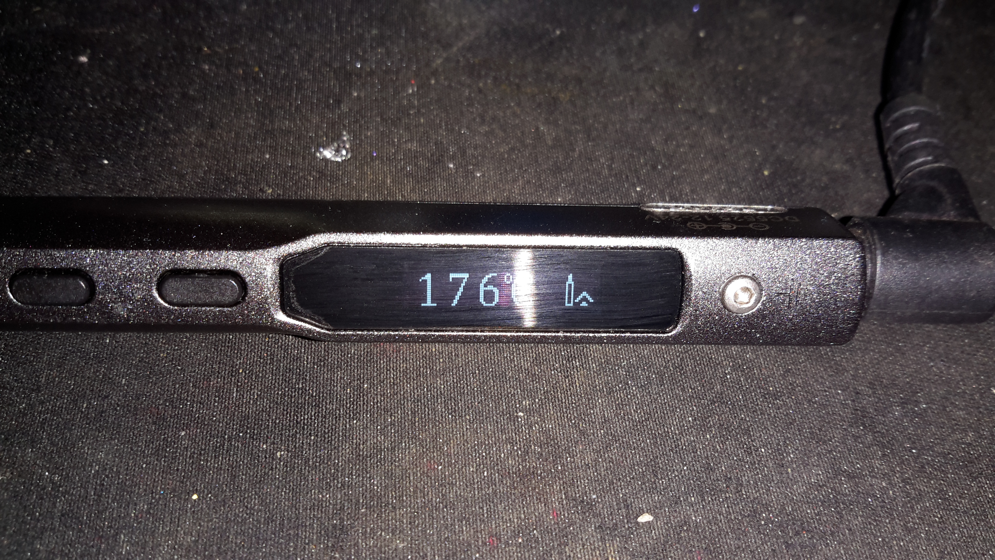
The left hand button starts the heater, which on a 24v input voltage gets to operating temperature well within 10 seconds.
Temperature Stable
The right hand screen icon changes when the temperature has stabilized. The control PCB has an integrated accelerometer, leaving the iron hot for a few minutes triggers a timeout & it powers down. Once picked up again, the heater instantly restarts.
The operating temperature is adjustable with the pair of buttons, from 100°C to 400°C.
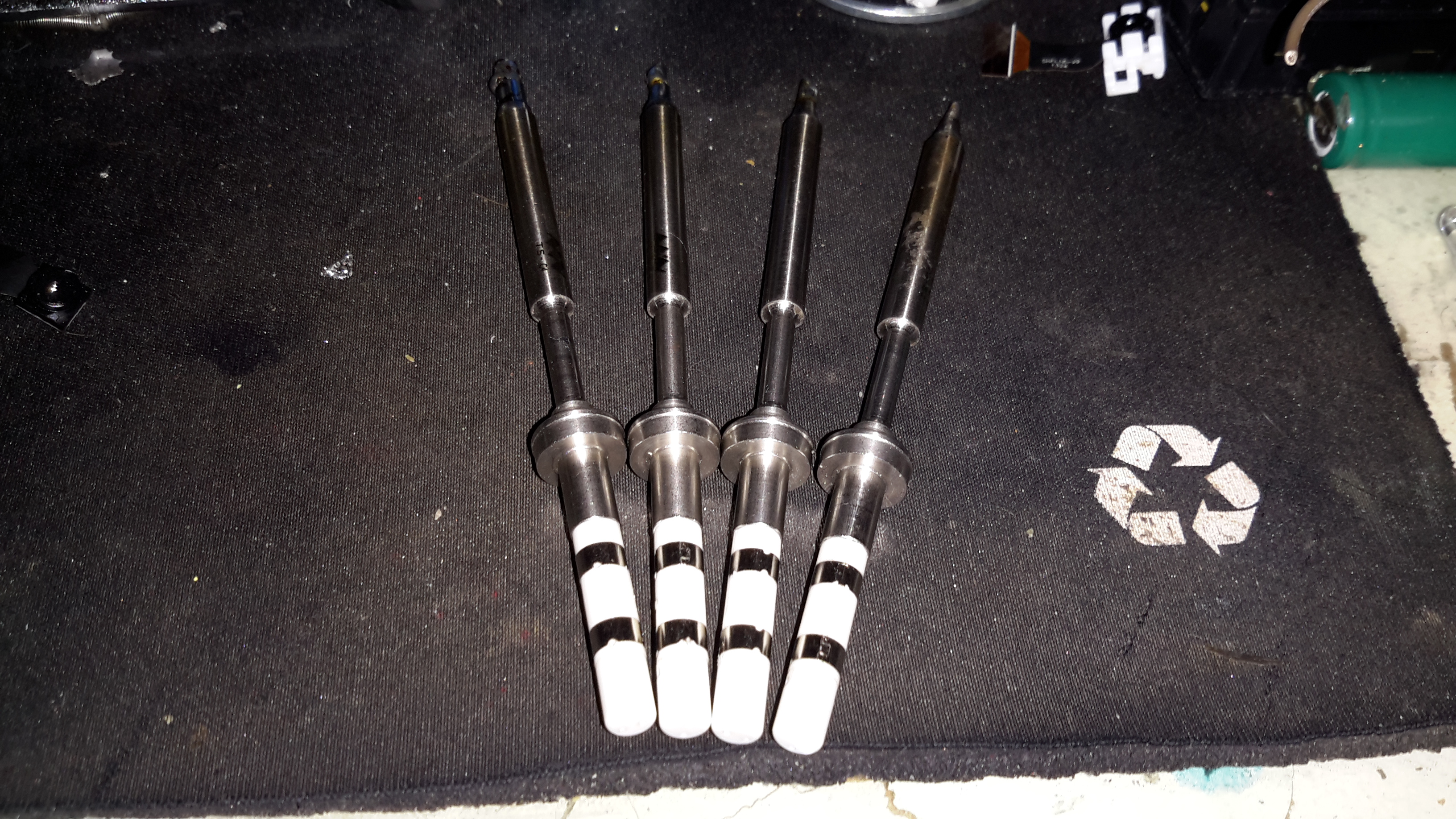
Different Bits
Here’s a selection of bits for the iron. The design is very similar to the Hakko T15 series of irons, but these are a much shorter version. Like the Hakko versions, the actual tips aren’t replaceable, once the bit burns out, the entire assembly is replaced.
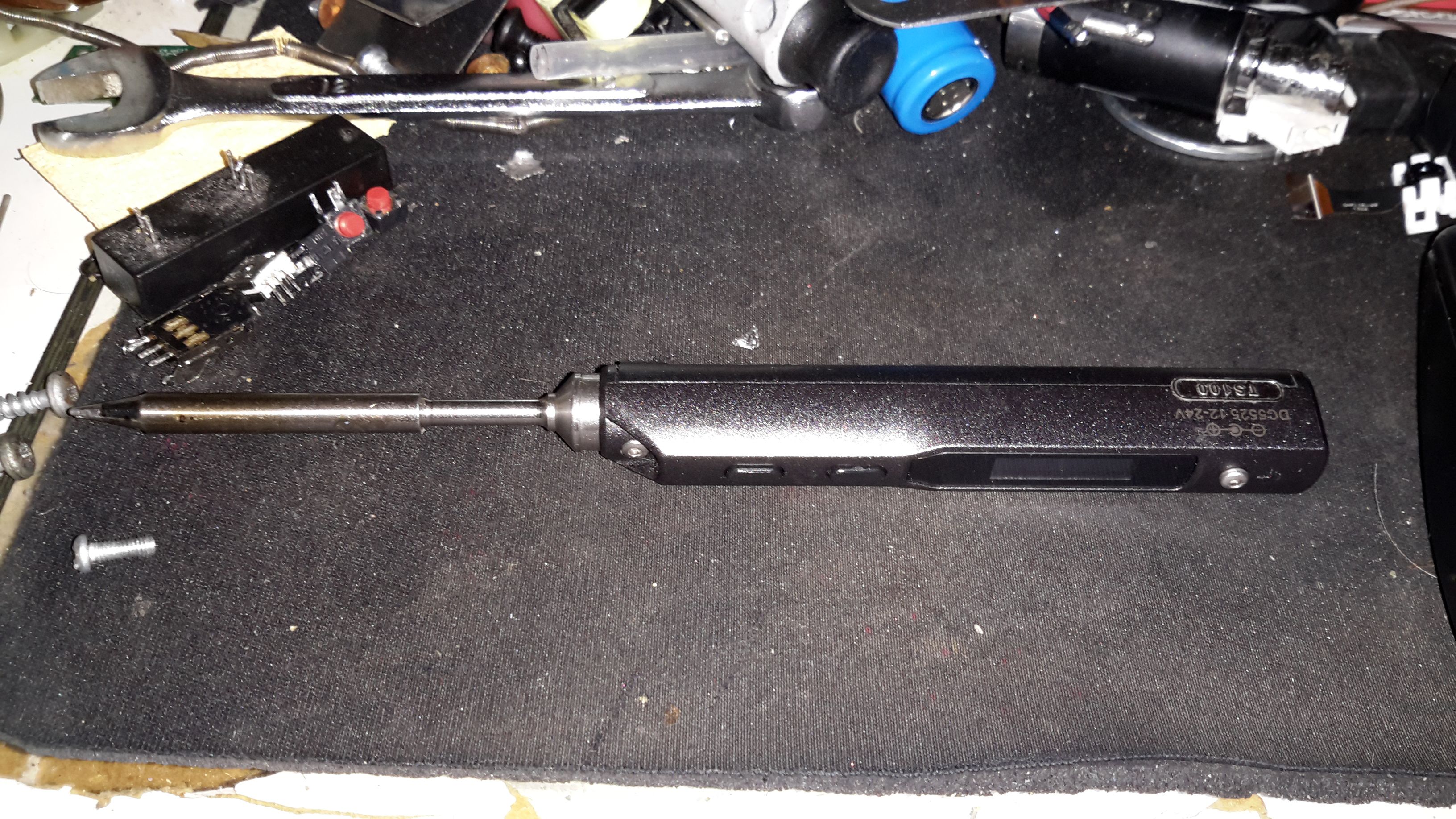
TS100 Soldering Iron
Here’s the iron fully assembled. The entire device is about the same length as just the heating element from a Hakko T15!
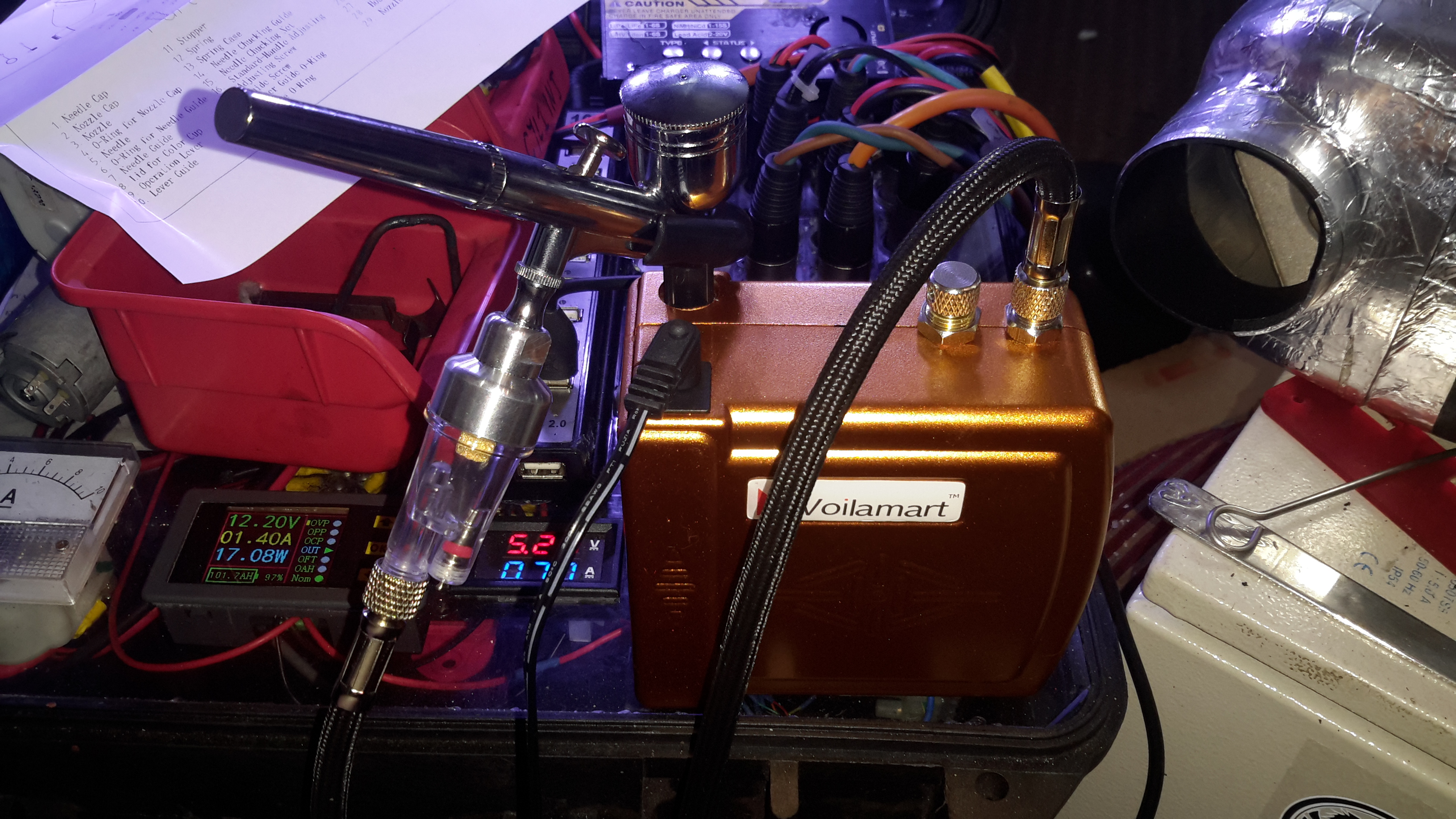
For my latest project, I needed an easier way to paint without messing about with brushes, and the associated marks they leave in a paint job. eBay provided me with a cheap airbrush & compressor.
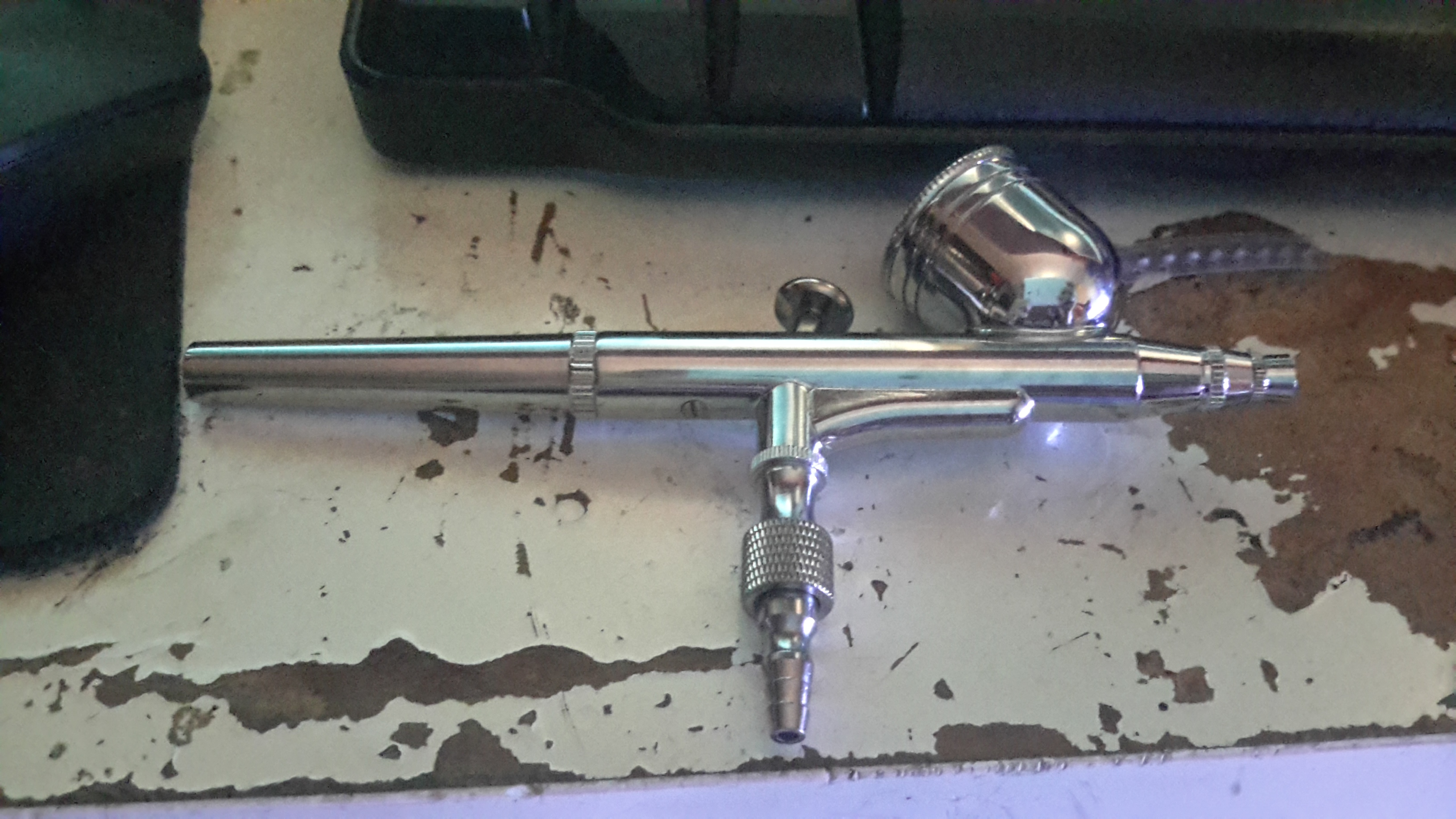
Airbrush Kit
For less than £30, this kit doens’t look so bad. I’ve never used an airbrush before, but I’ve had no problems with this as yet spraying both water based paints & solvent based paints.
Compressor
Here’s the compressor itself, this runs on 12v & has an output pressure of 1.5 Bar, which is supposed to be adjustable.
Compressor Internals
Removing a couple of screws reveals the internal components. Nothing much unusual here, a DC diaphragm pump, pressure switch & outlet fittings. There’s also a thermal cutout fitted next to the motor for protection.
The pressure switch attached to the manifold trips at 1.5Bar, keeping the pressure to the brush pretty much constant.
Air Block
Next to the air outlet fitting is an adjustment knob, supposedly for varying the pressure. However it’s just a piss-poorly designed adjustable relief valve that vents to atmosphere. There’s not much of a control range.
Messy Wiring
The wiring gets a bit messy where the power LED is concerned, with no heatshrink over the solder joints, but it’s adequate.
Airbrush
The airbrush itself isn’t too bad. It’s solid Brass, with a very nice Chrome finish. I’m not expecting miracles from a very cheap tool, but it certainly seems to be reasonable.
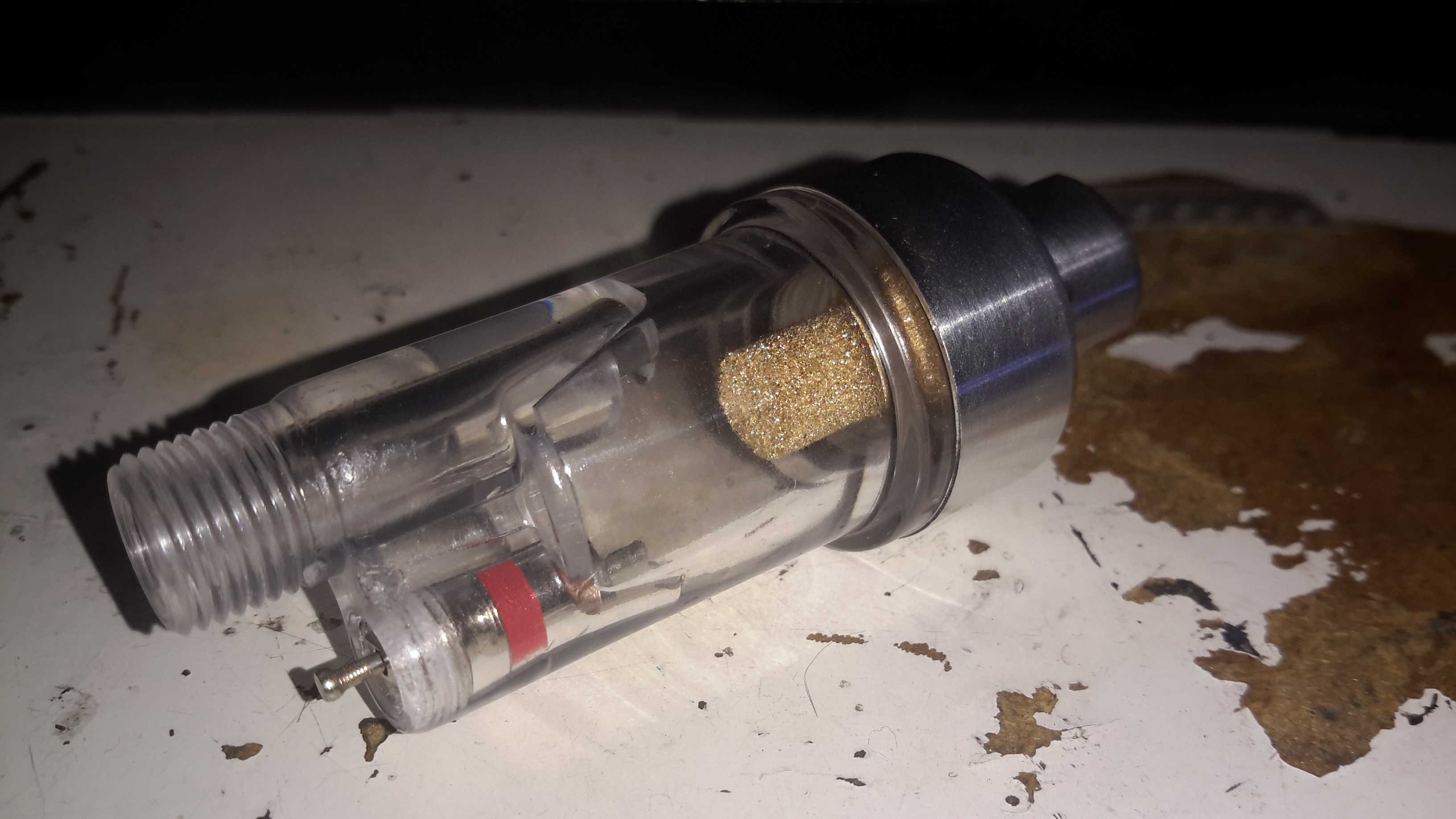
Water Trap
A moisture trap is supplied for the brush, to prevent water drops being sprayed out with the paint. Very handy.
I’m no fan of power inverters. In my experience they’re horrifically inefficient, have power appetites that make engine starter motors look like electric toothbrushes & reduce the life expectancy of lead-acid batteries to no more than a few days.
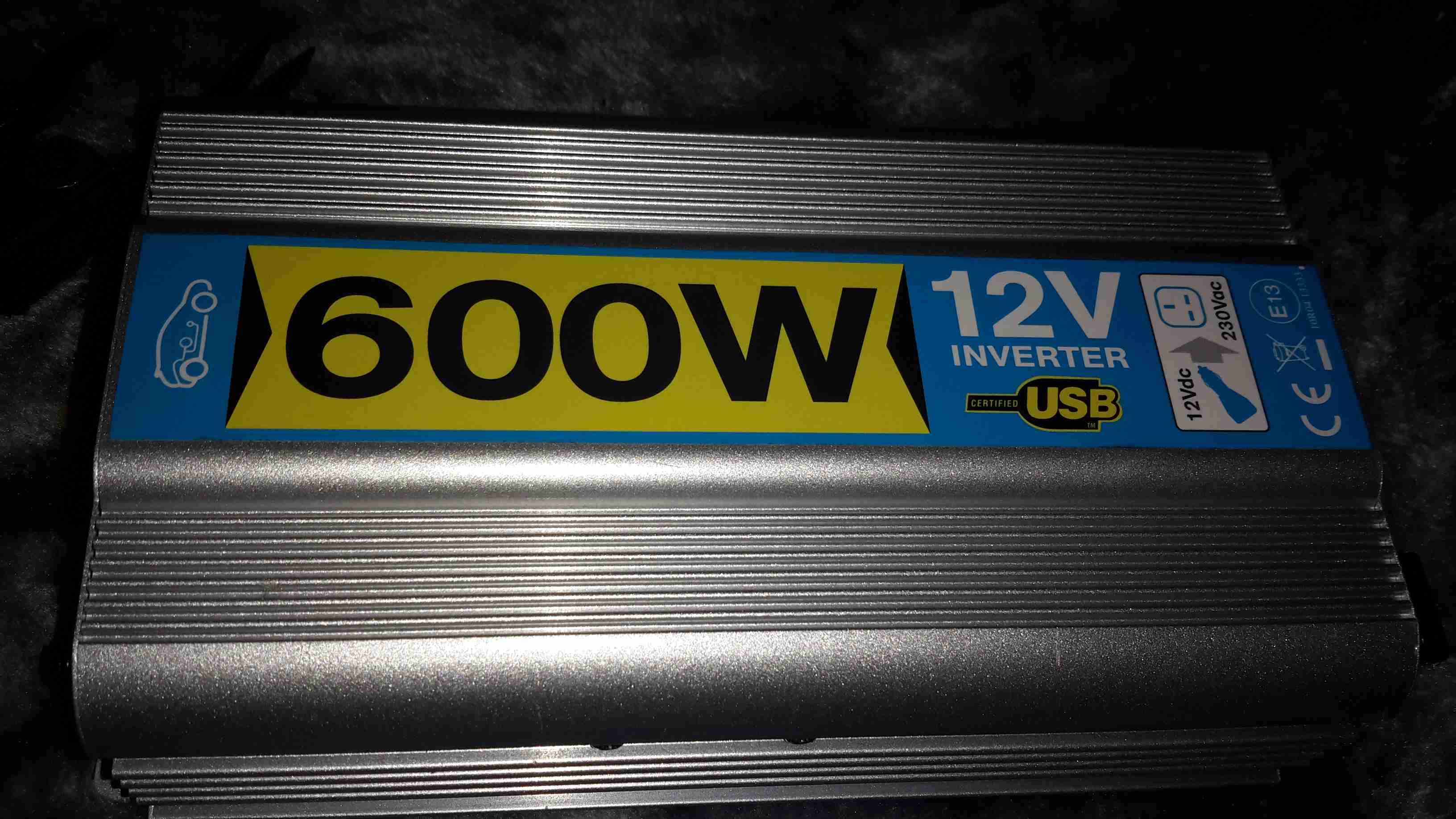
However I have decided to do a little analysis on a cheapo “600W” model that Maplin Electronics sells.
Cover Removed
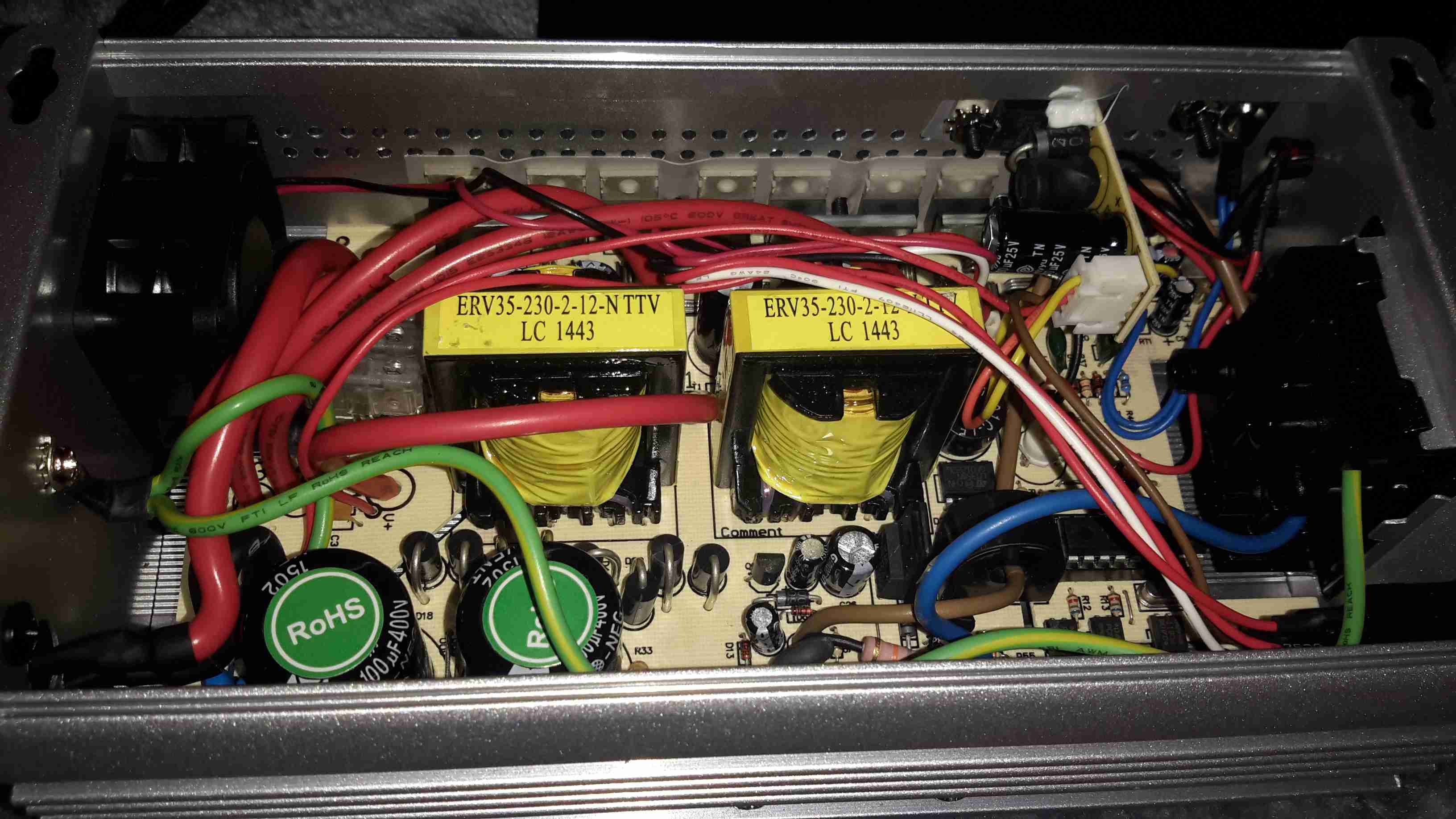
After a serious amount of metallic abuse, the bottom cover eventually came off. The sheet of steel used to close the bottom of the aluminium extrusion was wedged into place with what was probably a 10 ton hydraulic press.
As can be seen from the PCB, there’s no massive 50Hz power transformer, but a pair of high frequency switching transformers. Obviously this is to lighten the weight & the cost of the magnetics, but it does nothing for the quality of the AC output waveform.
DC Input End
The 12v DC from the battery comes in on very heavy 8-gauge cables, this device is fused at 75A!
DC Fuses
Here’s the fusing arrangement on the DC input stage, just 3 standard blade-type automotive fuses. Interestingly, these are very difficult to get at without a large hammer & some swearing, so I imagine if the user manages to blow these Maplin just expect the device to be thrown out.
Input DC-DC Switching MOSFETs
On the input side, the DC is switched into the pair of transformers to create a bipolar high voltage DC supply.
High Voltage Rectifiers
The large rectifier diodes on the outputs of the transformers feed into the 400v 100µF smoothing capacitors.
As mains AC is obviously a bipolar waveform, I’m guessing this is generating a ±150v DC supply.
Output MOSFETs
After the high voltage is rectified & smoothed, it’s switched through 4 more MOSFETs on the other side of the PCB to create the main AC output.
The label states this is a modified-sine output, so I’d expect something on the scope that looks like this:
Inverter Waveforms
Modified-sine doesn’t look as bad as just a pure square output, but I suspect it’s a little hard on inductive loads & rectifiers.
However, after connecting the scope, here’s the actual waveform:
Actual Waveform
It’s horrific. It’s not even symmetrical. There isn’t even a true “neutral” either. The same waveform (in antiphase) is on the other mains socket terminal. This gives an RMS output voltage of 284v. Needless to say I didn’t try it under load, as I don’t possess anything I don’t mind destroying. (This is when incandescent lamps are *really* useful. Bloody EU ;)).
About the only thing that it’s accurate at reproducing is the 50Hz output, which it does pretty damn well.
System Microcontroller
As is usual these days, the whole system is controlled via a microcontroller.
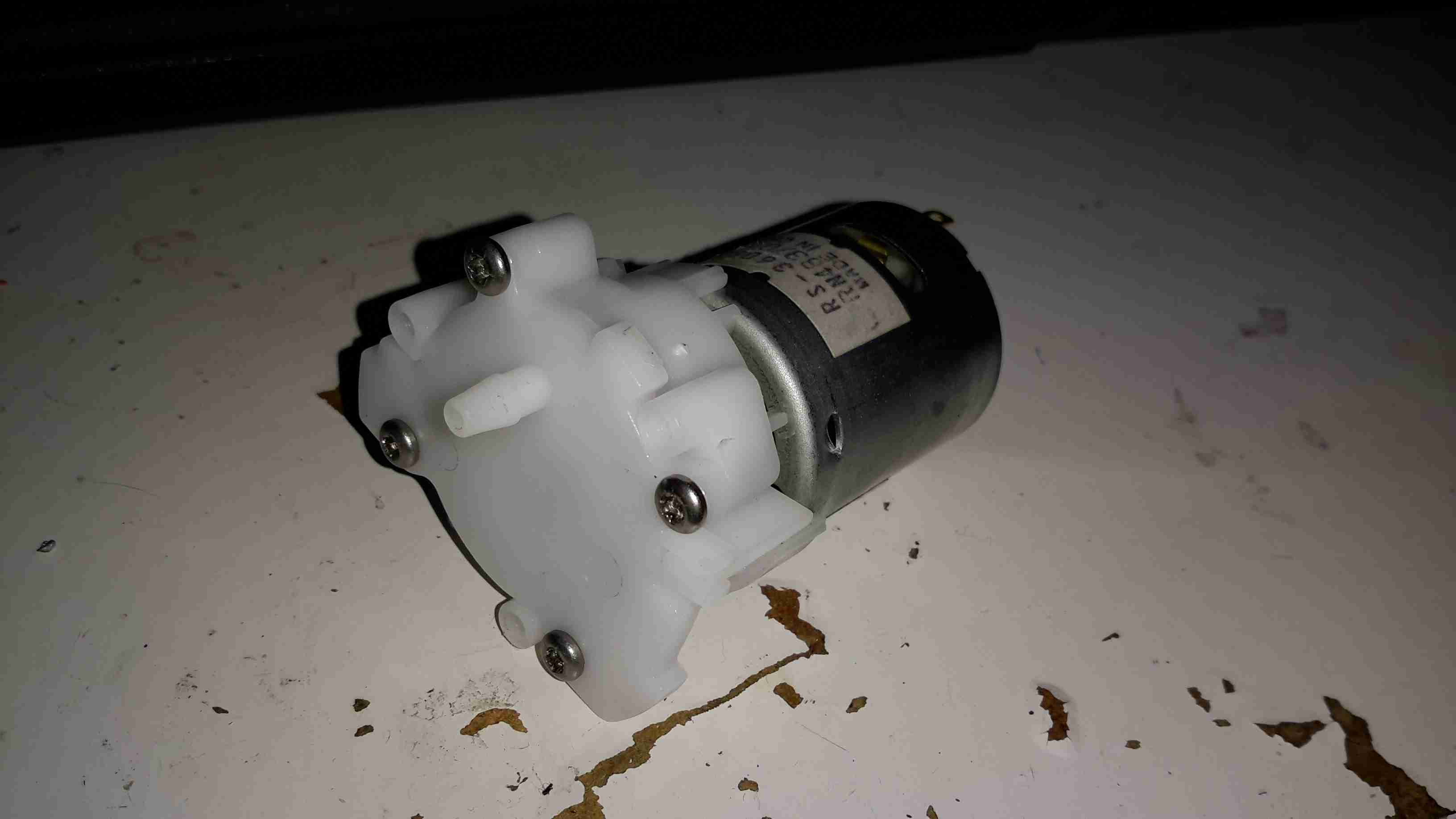
I got one of these to test since I’ve been in need of some small DC pumps for fluid transfer use. At £2 I can definitely afford to experiment.
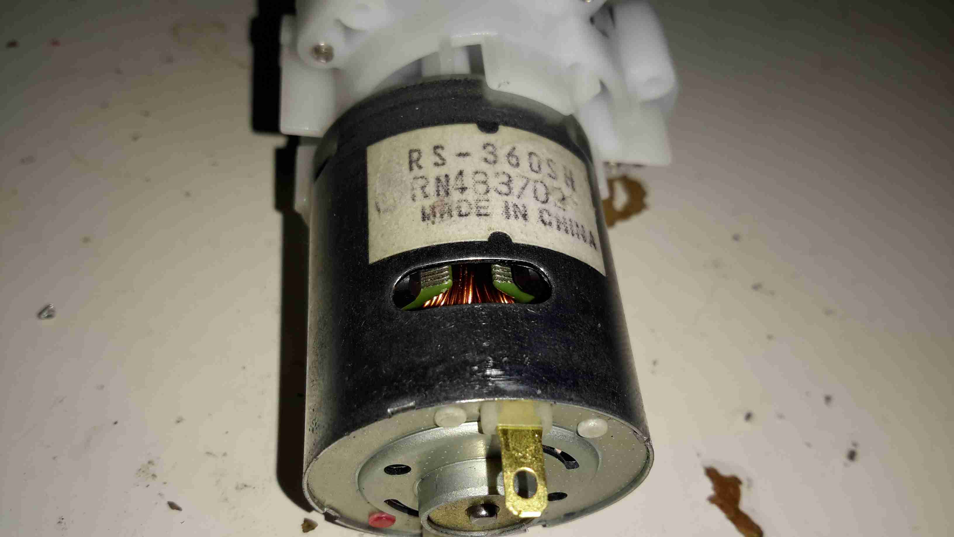
DC Motor
On the eBay listing, these pumps are rated at 3-12v DC, (I thought that was a bit wide of an operating range), I looked up the motor, an RS-360SH on Mabuchi’s website, they only have models in this range rated at 7.2v & 24v. Judging by the size of the windings on the armature & the fact that after a few minutes operation on 12v it gets rather hot, I’m going to say this is the 7.2v motor.
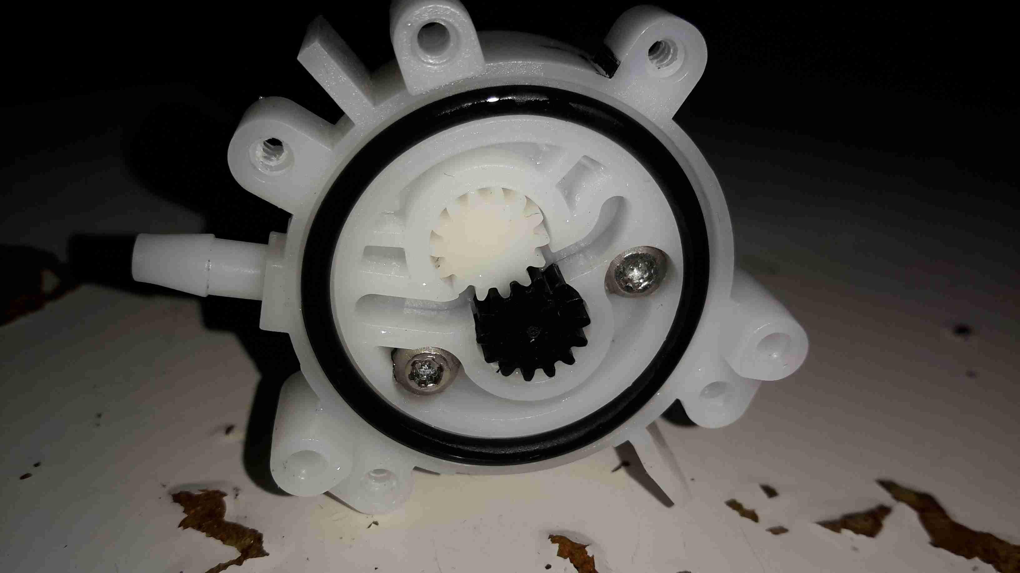
Pump Gears
Removing the screws releases the end cover & the pair of gears inside. This operates like any other hydraulic gear motor, albeit with much wider tolerances. It has no capability to hold pressure when the power is removed, and can be blown through easily.
Flow & pressure under power are quite good for the pump’s size, even though it’s noisy as hell.
Inkeeping with everything else in my shack being low voltage operated, I had planned from the outset to convert the desoldering station to 12v operation. It turns out this has been the easiest tool to convert in my shack so far.
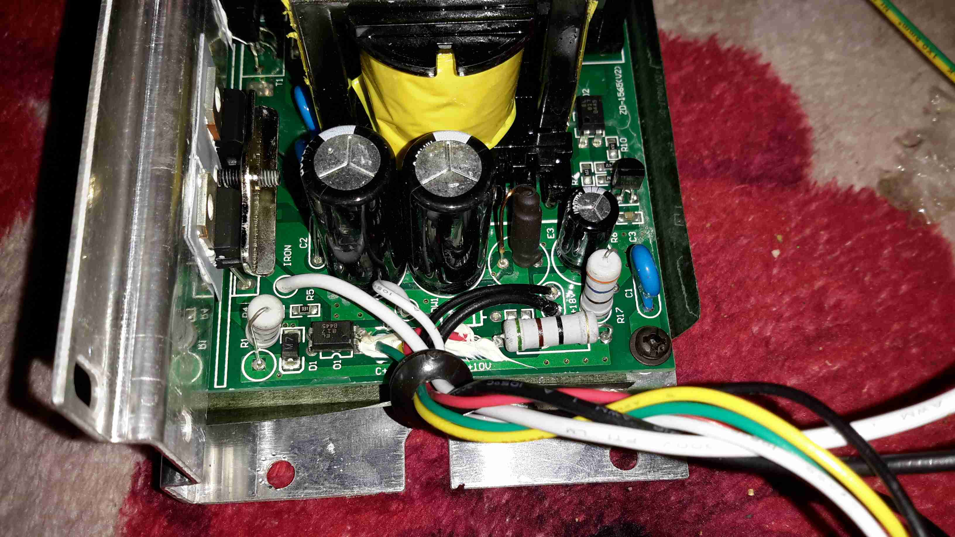
PSU Outputs
The factory SMPS is a fairly straightforward 18v 12A unit, with only a single small oddity: the desoldering gun’s heating element is controlled from inside the supply.
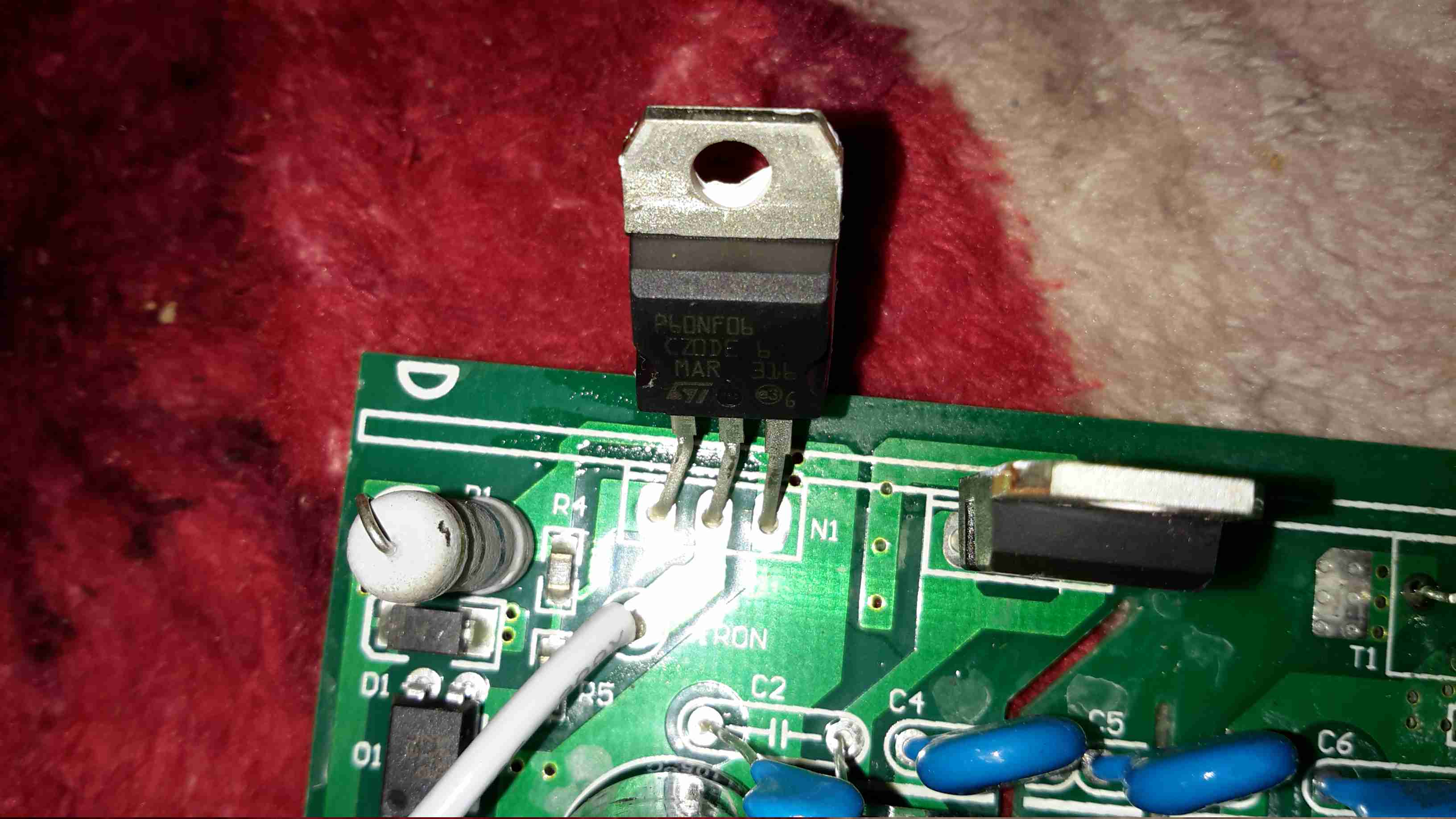
Iron MOSFET
Next to the output rectifier on the heatsink is a large MOSFET, in this case a STP60NF06 from ST Micro. This is a fairly beefy FET at 60v & 60A capacity, RDS On of <0.016Ω.
This is driven via an opto-isolator from the main logic board. I’ve not yet looked at the waveform on the scope, but I suspect this is also being PWM’d to control temperature better when close to the set point.
Iron Element Controller
Rather than fire up the soldering iron & build a new element controller circuit (Lazy Mode™), I opted to take a saw to the original power supply. I cut the DC output section of the PCB off the rest of the supply & attached this piece back to the frame of the base unit. I also added a small heatsink to the MOSFET to make sure it stays cool.
12v Power Supply
Since the fan & vacuum pump are both already 12v rated, those are connected directly to the DC input socket, that I’ve installed in place of the original IEC mains socket. The 18v for the heating element is generated by a 10A DC-DC converter, again from eBay.
Oddly, the iron itself is rated at 24v 80W, but the factory supply is only rated to 18v. I’m not sure why they’ve derated the system, but as the station already draws up to 10A from a 13.8v supply, increasing the voltage any further would start giving my DC supplies a problem, so it can stay at 18v for now.
Here’s another quick teardown, a cheap 5-port HDMI switch box. This is used to allow a single input on a monitor to be used by 5 different external HDMI devices, without having to mess about plugging things in.
Power & Remote
Here’s the DC barrel jack & 3.5mm TRS jack for power & remote control. There’s a little IR decoder & remote that go with this for hands free switching.
PCB Top
Here’s the PCB out of it’s plastic housing. The main logic is a pair of PI3HDMI303 3:1 HDMI switches from Pericom Semiconductor. These are cascaded for the 5-ports, the first 3 input HDMI ports are switched through both ICs to reach the output.
These HDMI switch ICs are operated with TTL input pins, the combination of these pins held either high or low determines the input port that appears on the output.
There’s a button on the left for switching between inputs, with a row of 5 LED indicators.
PCB Bottom
Not much on the bottom side, a lot of passives & bypass capacitors. There’s a 3.3v LDO regulator on the left for supplying the main rail to the active switch ICs. The IC on the right doesn’t have any numbering at all, but I’m presuming it’s a microcontroller, dealing with the IR remote input & pushbutton inputs to switch the inputs.
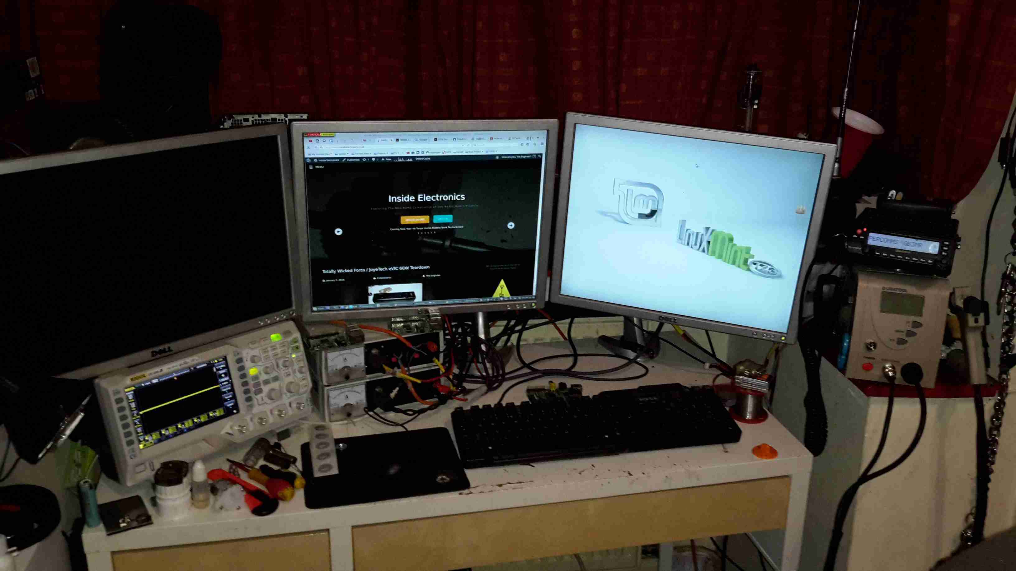
Main radio of course is housed on the left, it’s partially hidden under my currently over-populated breadboard.
All 3 monitors are linked to the same PC, using a pair of video cards. This is a very flexible system with so much screen real estate.
Main system power is provided by the pair of power supplies next to the radio – these are homebrew units using surplus switched mode PSU boards. Check my previous posts for more details.
Power Supplies
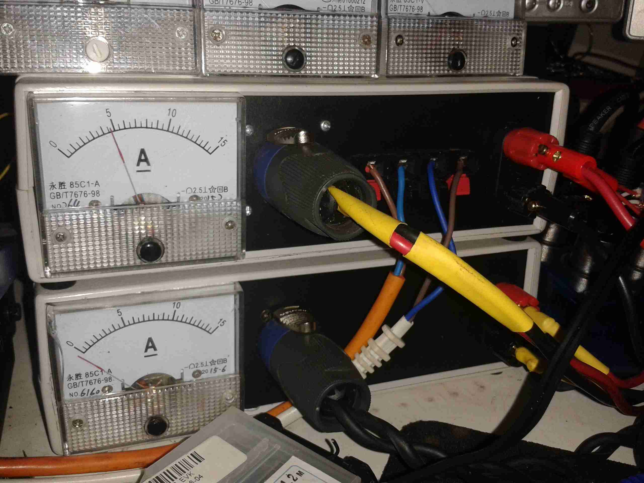
The mainpowersupply system. These two supplies are cross connected, giving a total DC amperage of 30A at 13.8v. There is also a link to a large 220Ah lead-acid battery bank (orange cable), to keep me on the air during power outages. This cable is getting upgraded to something more beefy shortly. The white cable is currently supplying power to my onlineradiation monitor.
The main high-currentDC outputs are the Speakon connectors next to the meters. The top one is powering the radio directly, the bottom is linked through to my 12v distribution box for lower current loads, such as the oscilloscope, audio amplifiers, tools, etc.
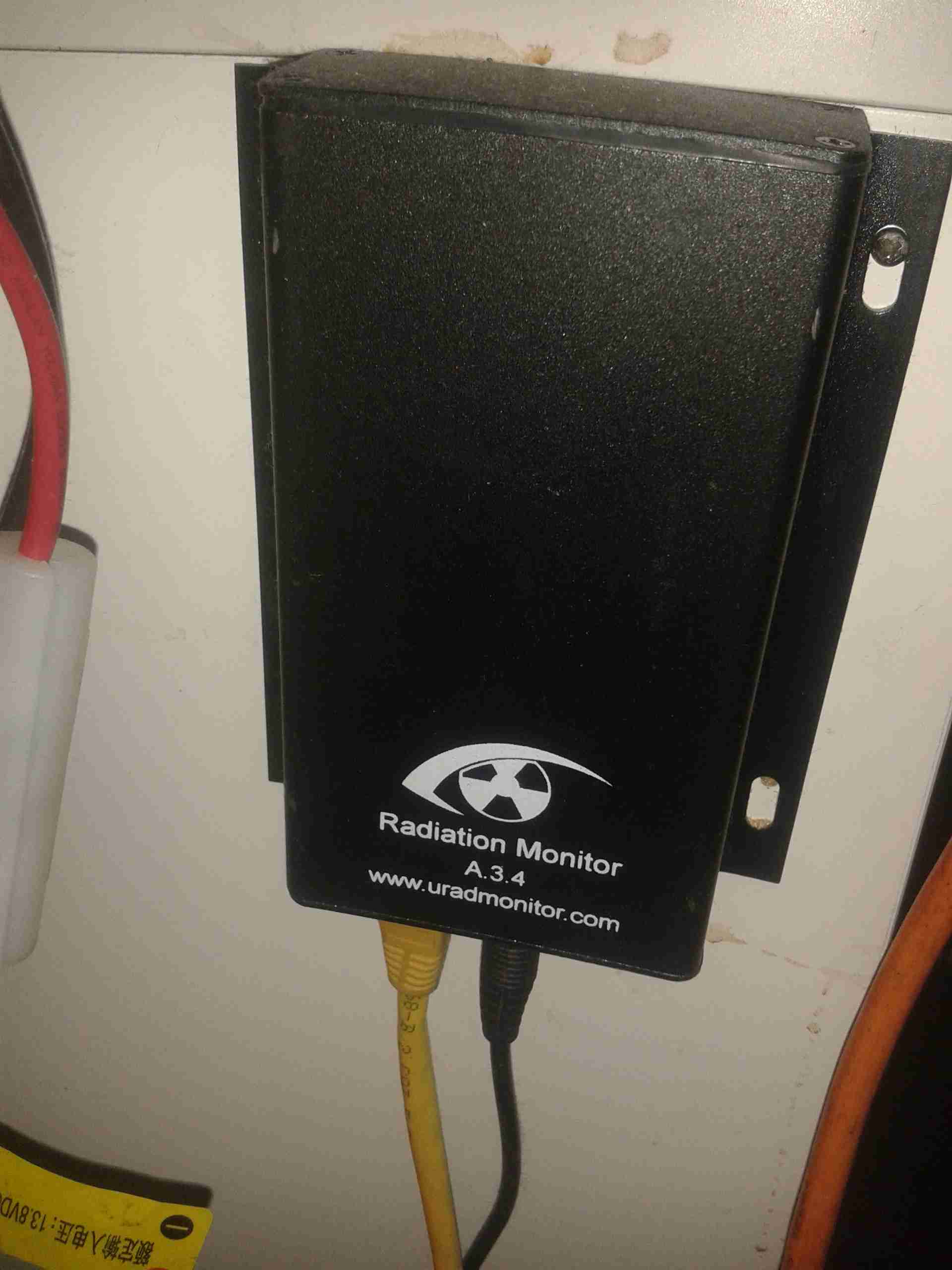
Radiation Monitor
Attached to the side of the desk is the radiation monitor itself.
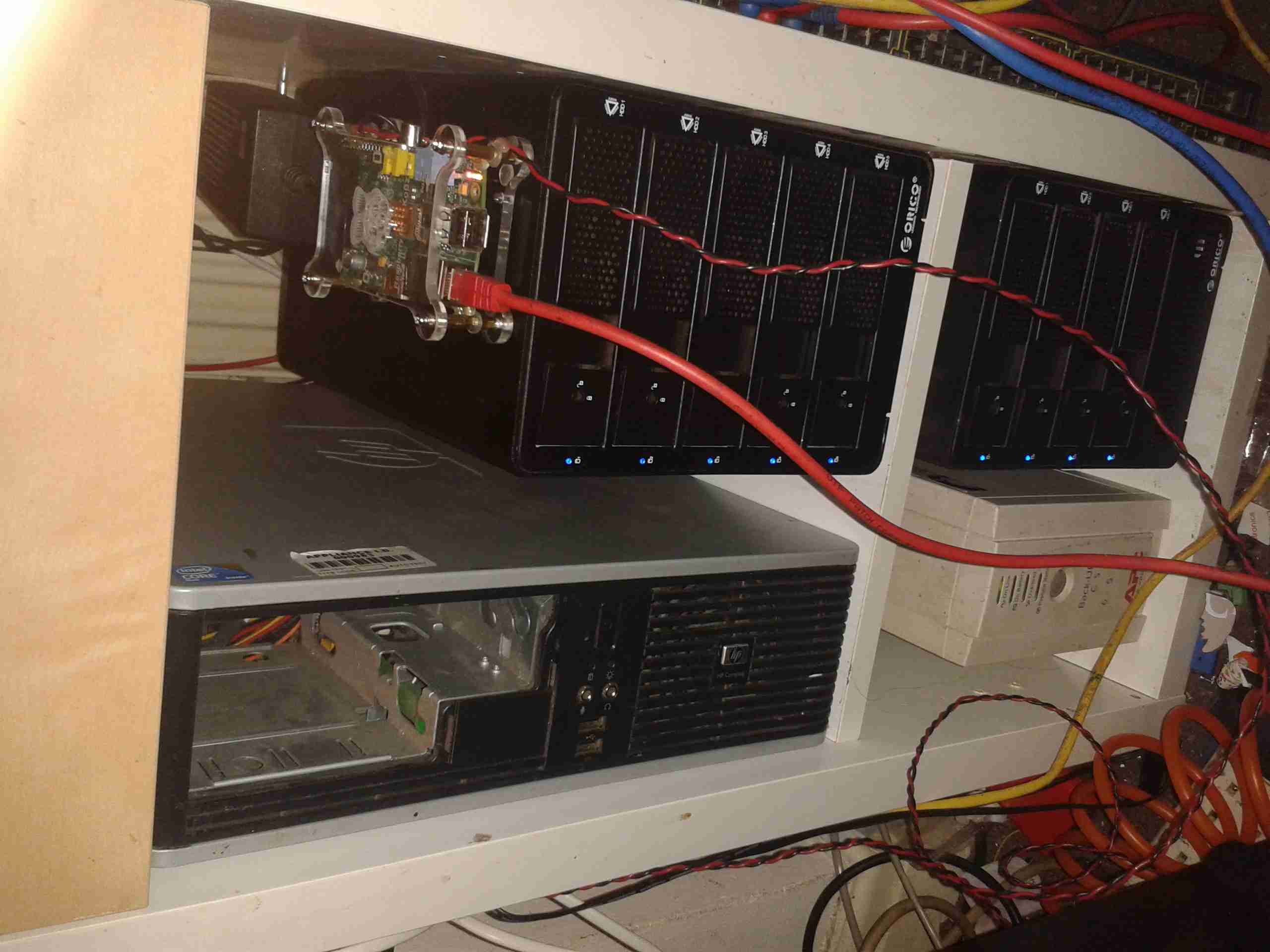
Core NAS
Under the radio is the core NAS of the network. It’s an array of 9 4TB disks, in RAID6, giving a total capacity after parity of 28TB. This provides storage & services to every other machine in the shack, the Raspberry Pi on top of the disk array is doing general network housekeeping & monitoring, also generating the graphs for the Radiation Monitor page. A Cisco 48-portswitch is partially out of frame on the right, providing 100MB Ethernet to the devices that don’t require gigabit.
I’ve had a couple of viewfinder CRT modules for a while, & haven’t done much with them, so I decided to make a very small B&W monitor.
CRT
I ordered a small transparent ABS box when I made a large order with Farnell, that turned out to be just about the perfect size for the project! The CRT & PCB barely fit into the space. The face of the CRT itself is about 17mm across.
Module Installed
Here’s the main PCB & tube fully installed into the case. Barely enough room for a regulator left over!
Power is provided by a simple LM7809 IC to take a standard 12v input.
Module Rear
Rear of the case, showing the fit of the control board.
Connections
Here’s the back of the monitor, with the DC input jack & a 3.5mm 4-pole jack for audio & video. This allows simple connection to many devices, including the one I’ll use the most – the Raspberry Pi.
Completed
Completed monitor. Audio is handled by a very small 20mm speaker, currently mounted just below the CRT face.
Current draw from a 13.8v supply is 117mA.
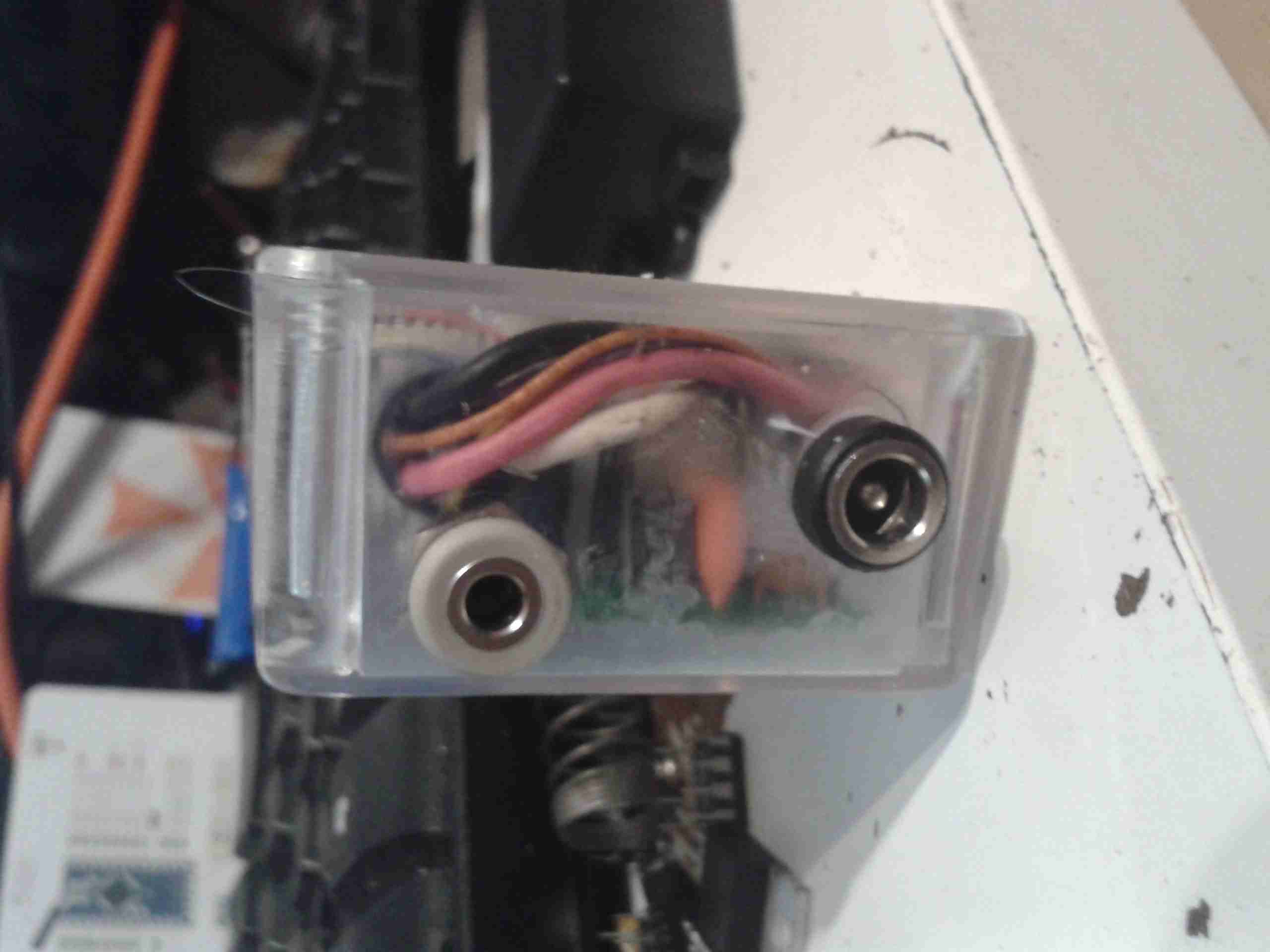
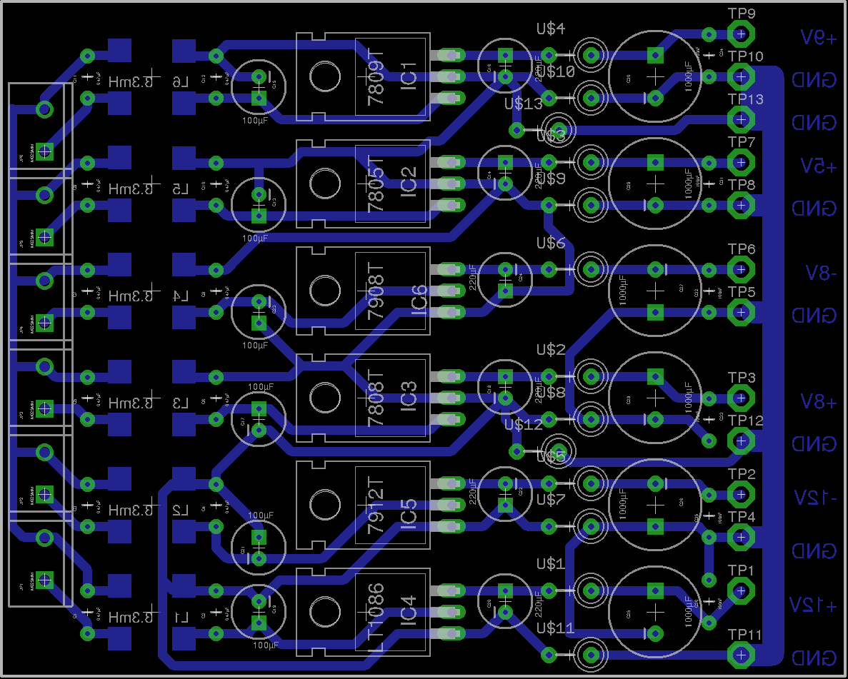
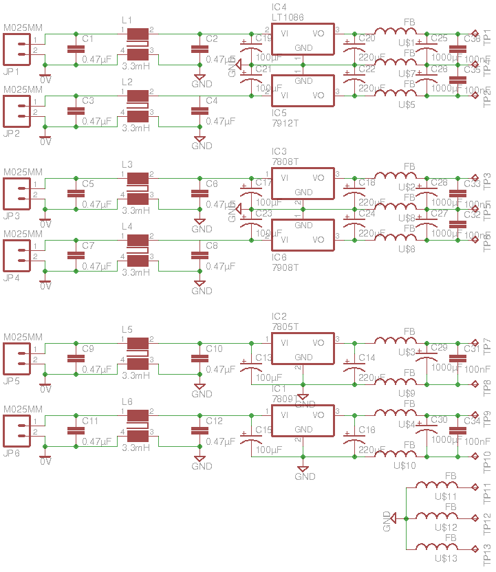
Finally, here’s the last part of the Rigol 12v DC Power Supply project, the linear post regulation section to remove some of the ripple.
I have made a couple of layout adjustments since the last post about this part of the project – a little more filtering on the DC outputs. As usual the Eagle project files are at the bottom of the post for those who might find them useful.
Updated PCBUpdated Schematic
Completed PCB
Here’s the completed PCB, partially installed in the back of the scope. The missing regulator is the 5v one, since I already have a source of clean 5v from my original attempt at the supply, it’s not a problem not using a linear after the switcher. The filtering is the same on all channels, input from the switchers is on the right, outputs to the scope on the left.
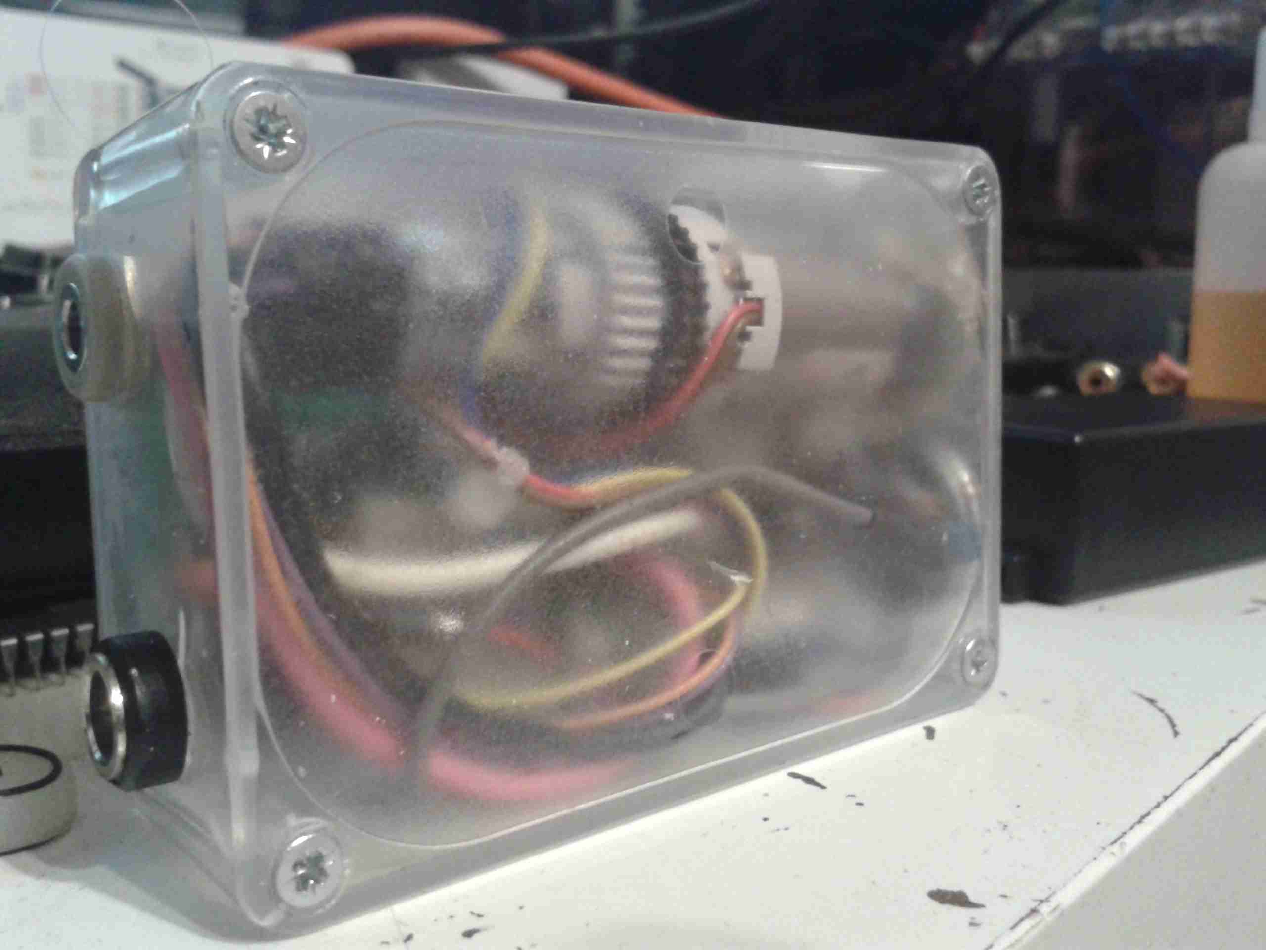
PCB Bottom
Here’s the bottom of the PCB, with the common mode input chokes. The design of this board has allowed me to remove a couple of the switching modules as well, as I can use a single bipolar supply to run both sets of bipolar regulators on this board. This should help remove some of the noise also.
The ripple level has now dropped to lower than it was originally on the mains supply! Current draw at 13.8v DC is about 1.75A.
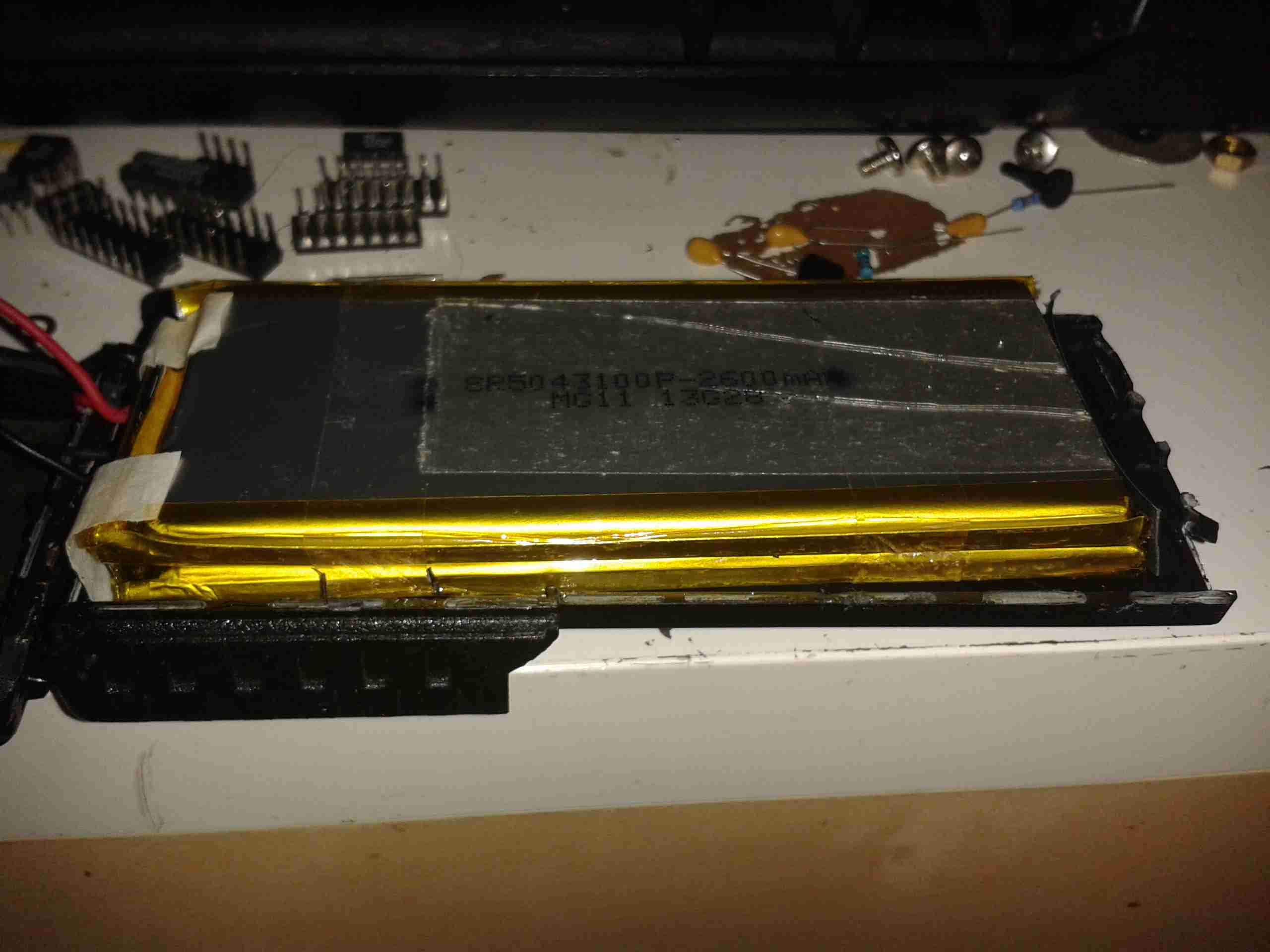
I’ve had a couple of larger batteries for my UV-5Rs for some time now, and decided to do a quick teardown to see if they’re actually the capacity claimed.
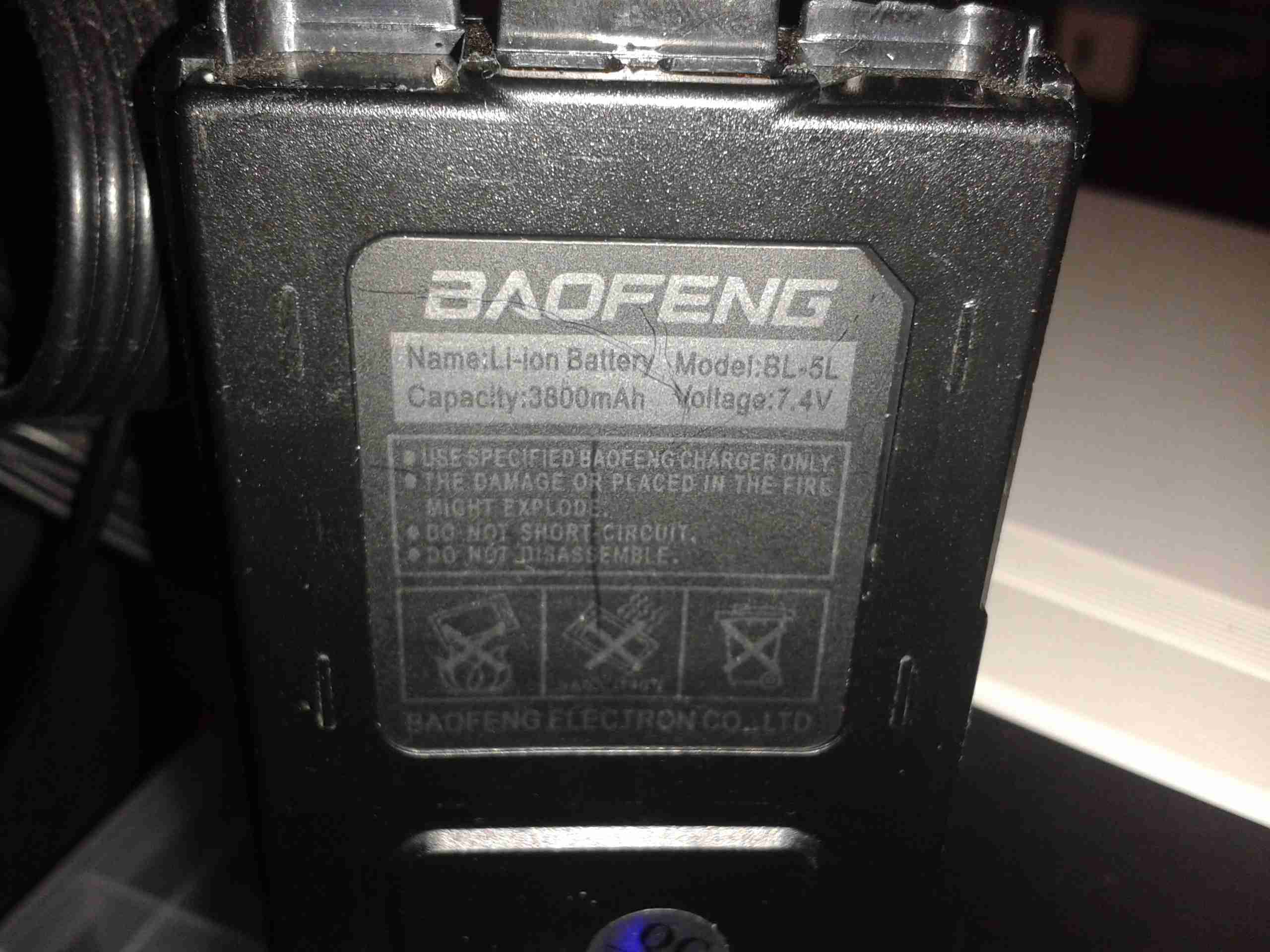
BL-5L Battery
Here’s the label, claiming 3800mAh (3.8Ah) of battery capacity.
These batteries are held together with glue, but a good way to get these kinds of things open is by whacking the seams with the handle of a screwdriver. This cracks the glue without damaging the casing.
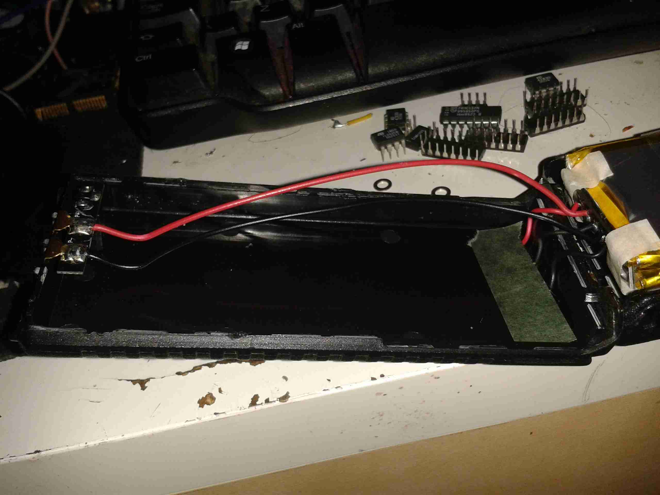
Battery Cracked Open
After a few minutes of cracking the seams, the battery comes right open. The pair of wires link the protection board on the cells to the DC terminals on the top of the pack. The charging terminals are under the cardboard insulator on the right.
Cells
Here’s the other half of the case, with the cells themselves. These are wired in series for a 7.2v pack, and at a capacity of 2600mAh (2.6Ah) printed on them, the label clearly lies about the capacity.
Tip Jar
If you’ve found my content useful, please consider leaving a donation by clicking the Tip Jar below!
All collected funds go towards new content & the costs of keeping the server online.