Posted on Leave a comment

SDR FM Broadcast Stopband Filters

There’s a common problem with all Software Defined Radios – their input stage is wide open, and therefore susceptible to desensitisation by local high power transmitters. The main culprits are broadcasts in the FM band, from 88-108MHz. Commercial stopband filters are available to solve this issue, by cutting out the FM Broadcast band. Before I ordered a commercially produced filter, I figured I’d try my hand at building my own.

DIY Stopband Filter
DIY Stopband Filter

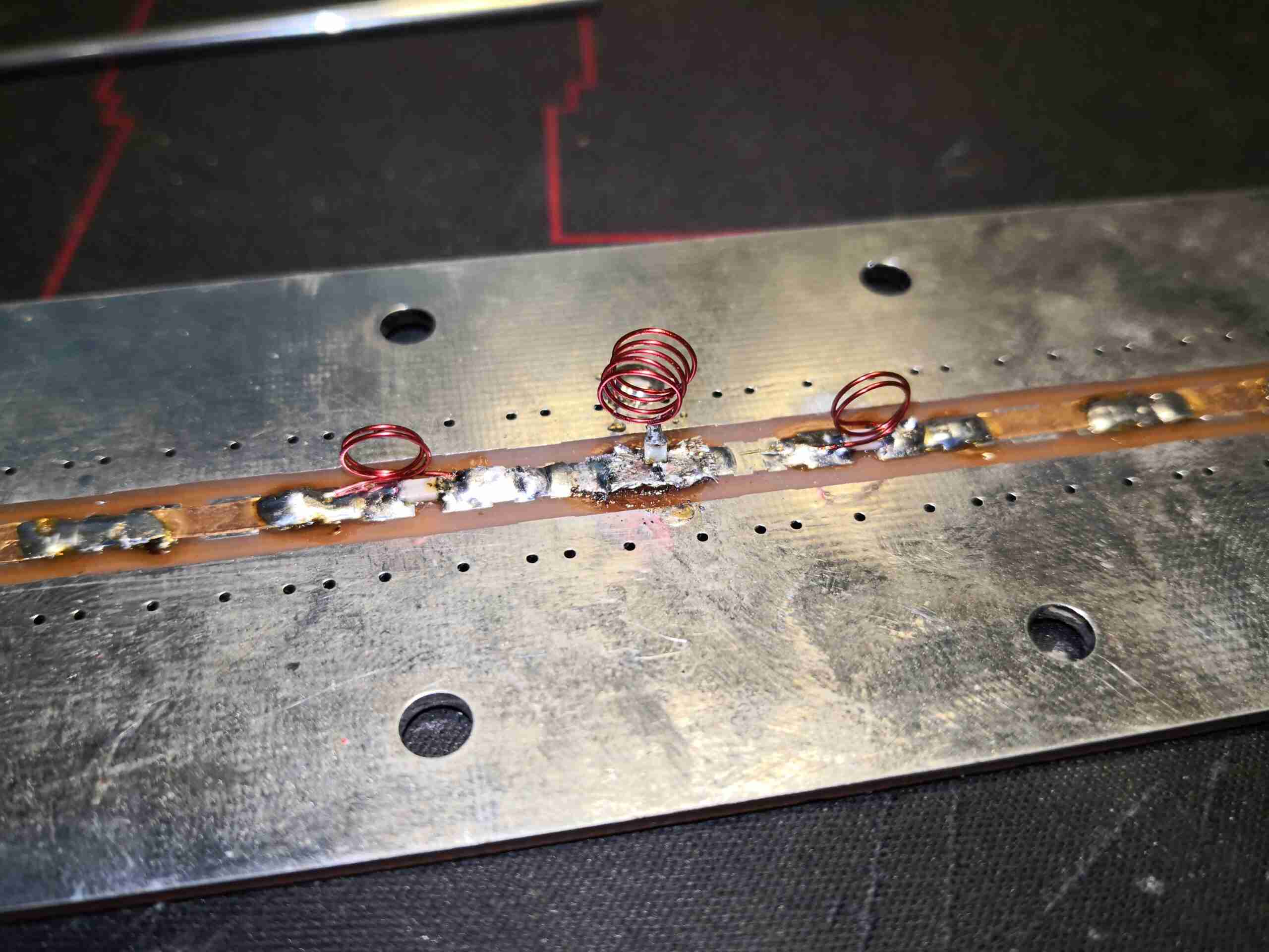
Here’s the filter I came up with, a Type 2 Chebyshev. It’s built on a prototype stripline PCB, with SMA connectors at either end for I/O. This was created with the help of a filter calculator, the response of the filter can be seen below:

Filter VNA Performance

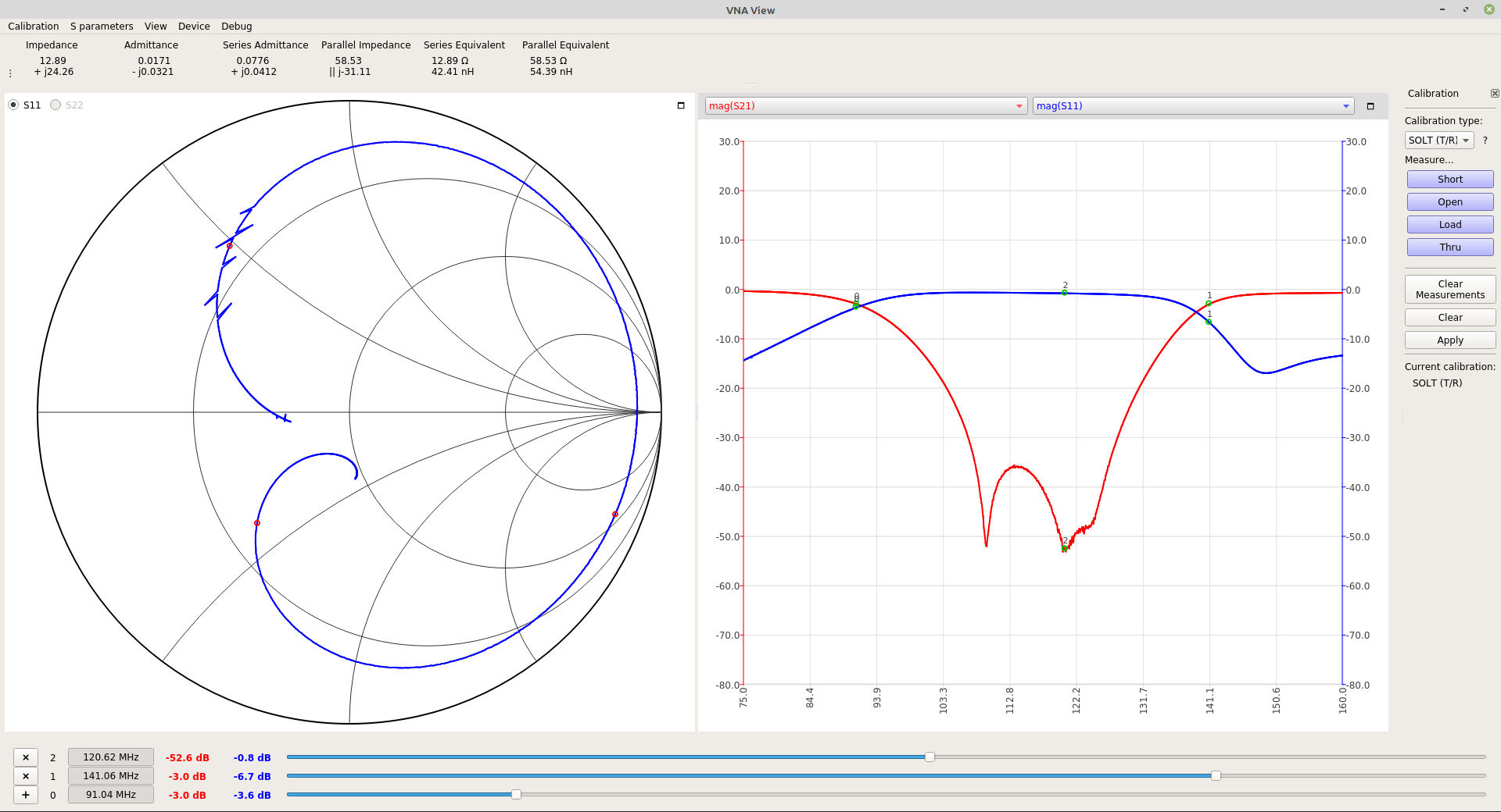
The response of the filter isn’t bad at all! It’s shifted up a little high on the scale, with the lower -3dB point being at 91MHz rather than 88MHz, but it does indeed chop out the broadcast band by -52dB. The high -3dB point is at 141MHz.

Let’s look at a commercial filter now, here’s the unit below, it’s definitely been size & cost optimized!

Commercial Stopband Filter

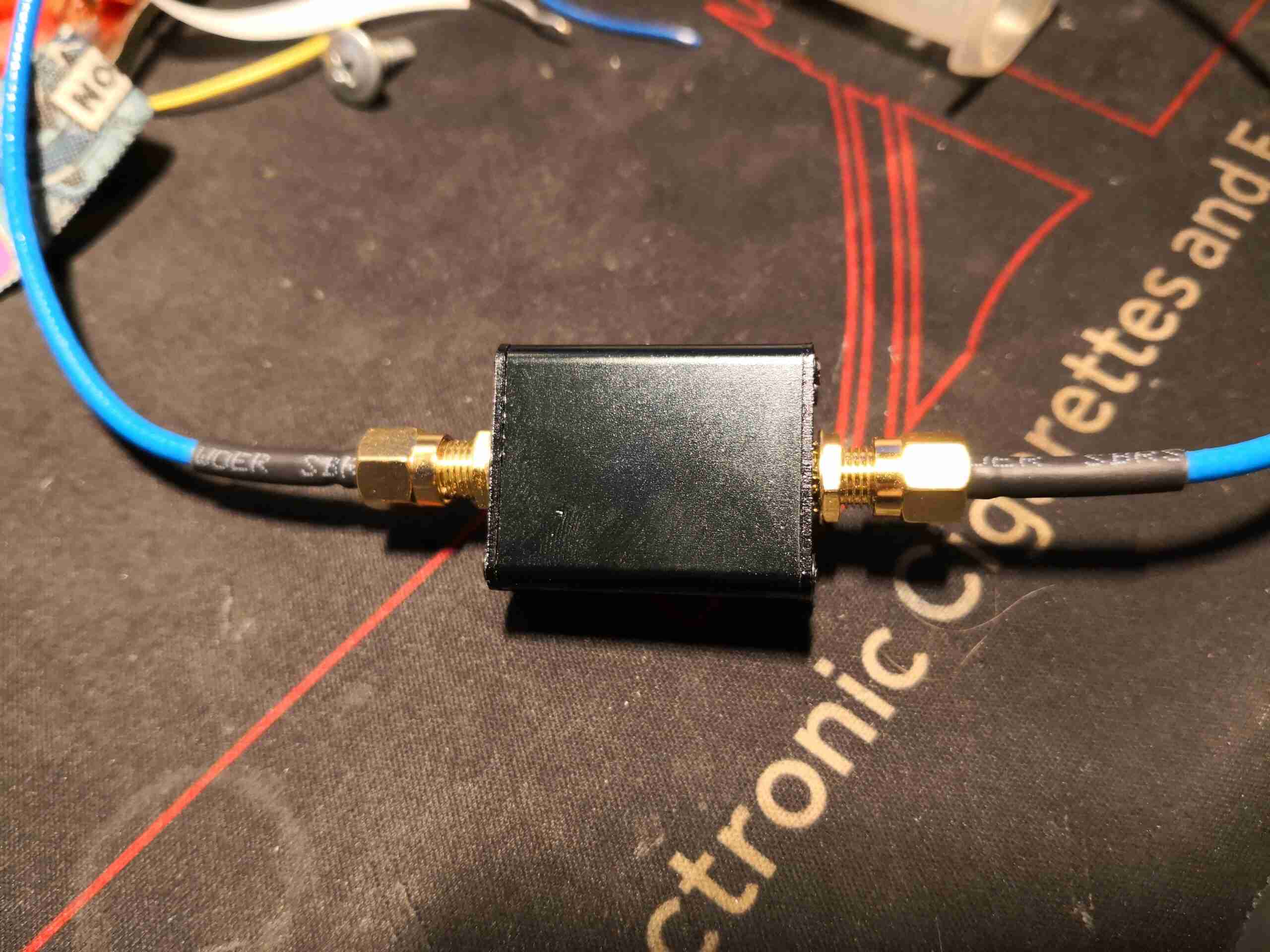
The box is tiny, not much bigger than the SMA connectors!

Commercial Filter VNA Characteristics

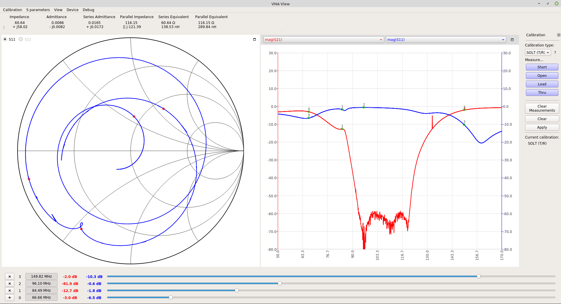
Looking at the plot from the NanoVNA, it’s clear this is also a Type 2 Chebyshev, but it’s more effective. This has a stopping power of -82dB, it’s also better centred.

Commercial Filter PCB

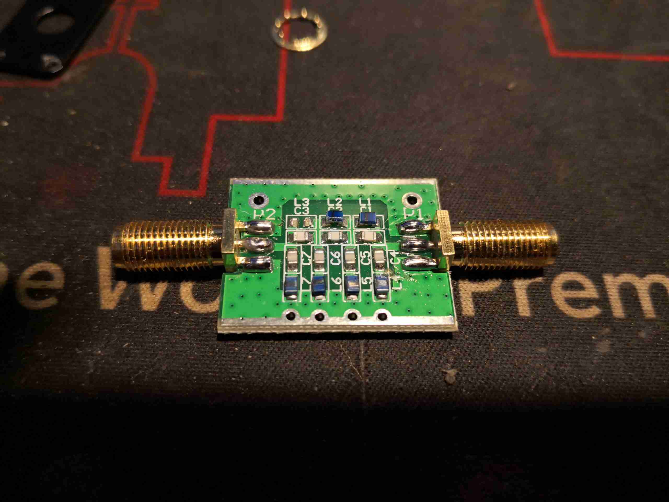
The board easily removes from the external shell. The SMA connectors are edge launch, which is good for maintaining impedance. There are a couple more stages of filtering in here than I put on my filter, which explains the much improved blocking characteristics. There does appear to be some damage though – there’s an inductor missing from the left side of the PCB. This is probably responsible for the odd response at the low end. There clearly was an inductor there, as the solder fillets are still present. Maybe this was removed at the factory as a form of tuning?

Posted on 3 Comments

NanoVNA-Qt Raspberry Pi AppImage Build

There’s quite a nice desktop app for the new NanoVNA v2, NanoVNA-Qt. It’s released as an AppImage for Linux, but unfortunately there is no version to run on a Pi supplied. The version below is built to run on the latest version of Raspbian (as of writing this, 2020-05-27).

Enjoy!

Posted on Leave a comment

HP 8753C Display LCD Replacement

Completed Install
Completed Install

Since I inherited an old HP 8753C Network Analyser from work, I figured updating a few things to relatively modern standards would be good. The factory CRT, being 28 years old, is definitely getting a little tired, not to mention being slow to warm up. I read over on the EEVBlog forums about a DIY modification to integrate an LCD display into place instead. There was also the option of a ready-made kit for these instruments which would integrate an LCD, but the cost at over £300 was very prohibitive!

CRT Pinout
CRT Pinout

The CRT display unit is a self-contained Sony unit, taking RGBHV signalling from the graphics control card of the analyser. Power is 65v DC which will definitely come in handy for powering the new LCD & control gear, after some conversion.

Test Wiring
Test Wiring

Doing a quick test with some wiring stuck into the video connector from the graphics controller, proved that I could get a decent video signal out of the unit! The only signals used here are RGB, along with the vertical & horizontal sync.

GBS-8200 Converter Board

The video is converted to VGA by way of a GBS-8200 arcade machine video conversion board, which will take many different video formats & spit out standard VGA signalling. The power supply to the left is a standard 100-240v to 12v PSU, which is happy to run at 6t5v DC input voltage, albeit with a ~5 second delay on output startup when power is applied. This is due to the massive 6.6MΩ resistance of the startup resistor chain, which I did reduce by 50% to 3.3MΩ with no effect. Since it does start OK even with the delay, I think I’ll not tinker with it any further. I doubt I could pull the full rated power from it with such a low input voltage, but all included, this mod draws less than 600mA at 12v.
A custom 20-pin IDC cable was made up to connect to the analyser’s graphics board, and this was then broken out into the required RGB & sync signals. Quite a few of the grounds are unused, I’ve not yet noticed any issues with EMC or instability.

Sync Combiner
Sync Combiner

There is a quad-XOR gate deadbugged to the PCB, which is taking the separate sync signals & combining them into a composite sync. The conversion board does have separate sync inputs, but for some reason doesn’t sync when they’re applied separately. This gate IC is powered from the 3.3v rail of the converter board, with the power lines tacked across one of the decoupling caps for the DRAM IC.

LCD Control PCBs
LCD Control PCBs

The donor 8.4″ LCD came from eBay in the form of a POS auxiliary display. I pulled the panel from the plastic casing, along with the control boards, and attached them all to the back. This LCD also had a sheet of toughened glass attached to the front, no doubt to protect against the Great Unwashed while in use! This was also removed.

Control Boards Mounted

A cut piece of plexiglas allows the boards to be mounted in the cavernous space the CRT once occupied, with some brass standoffs. 12v power & VGA are routed down to the LCD on the front of the analyser.

LCD Wiring
LCD Wiring

The LCD itself is tacked in place with cyanoacrylate glue to the securing clips for the glass front panel, which is more than enough to hold things in place. The input board which just has the VGA connector & power connector is glued edge-on to the metal back panel of the LCD, and is under little strain so this joint should survive OK.