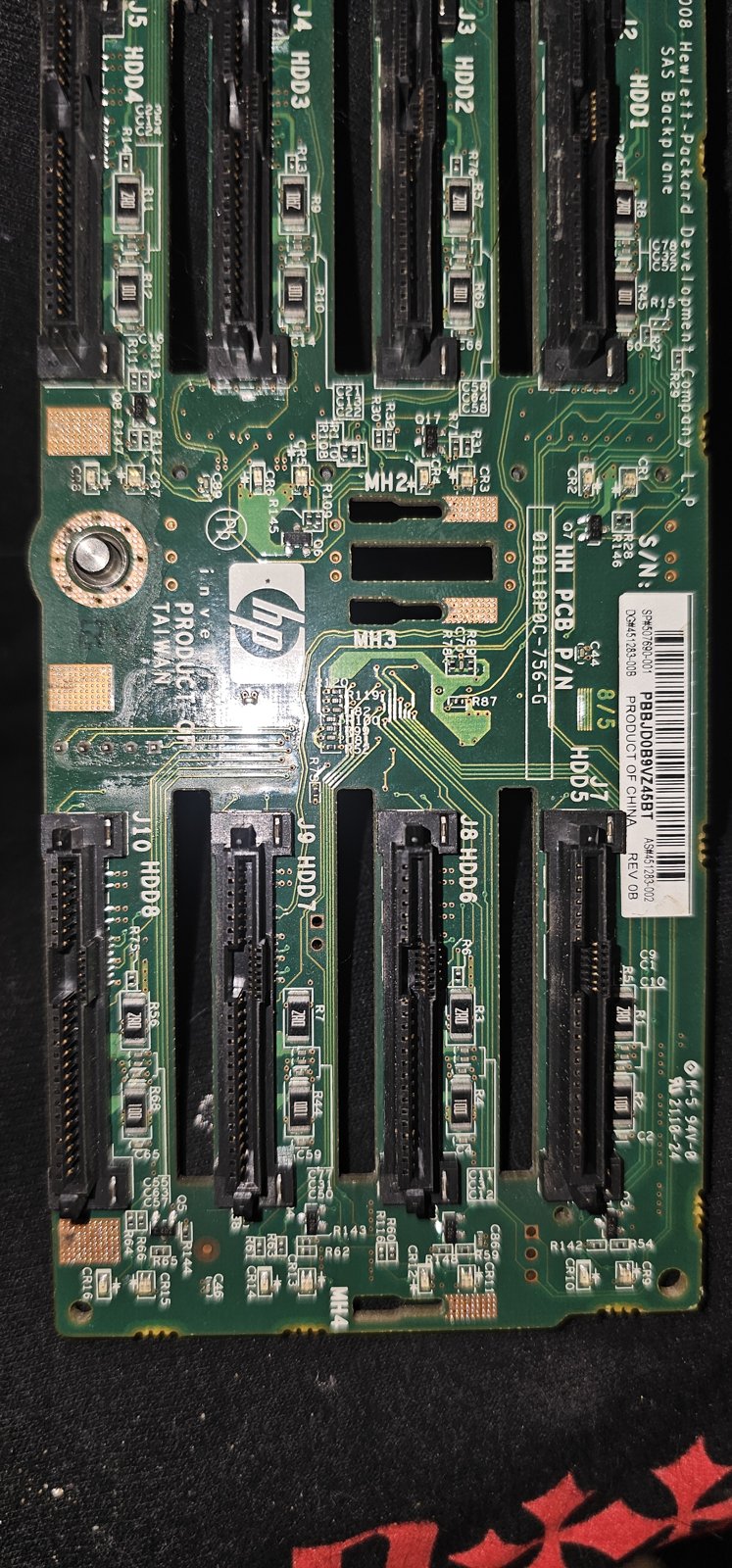
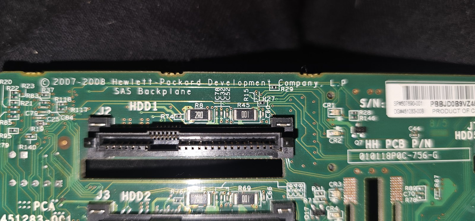
I’m building a 2U NAS around two HP DL380 G7 eight-bay small form factor drive cages, and each cage comes with an HP 496074-001 SAS backplane. The drives sit happily on it, but the three little LEDs in each bay (blue, green and amber) are controlled by two tiny microcontrollers speaking a proprietary protocol, and I wanted to drive them myself. So this turned into a reverse engineering project: work out how the backplane really works, replace its firmware with something I understand, and draw the schematic, because I couldn’t find a published one.
This is a long post because it covers a few days of poking. Everything here was measured on my own boards. Where I’m guessing, I say so.
What’s on the board
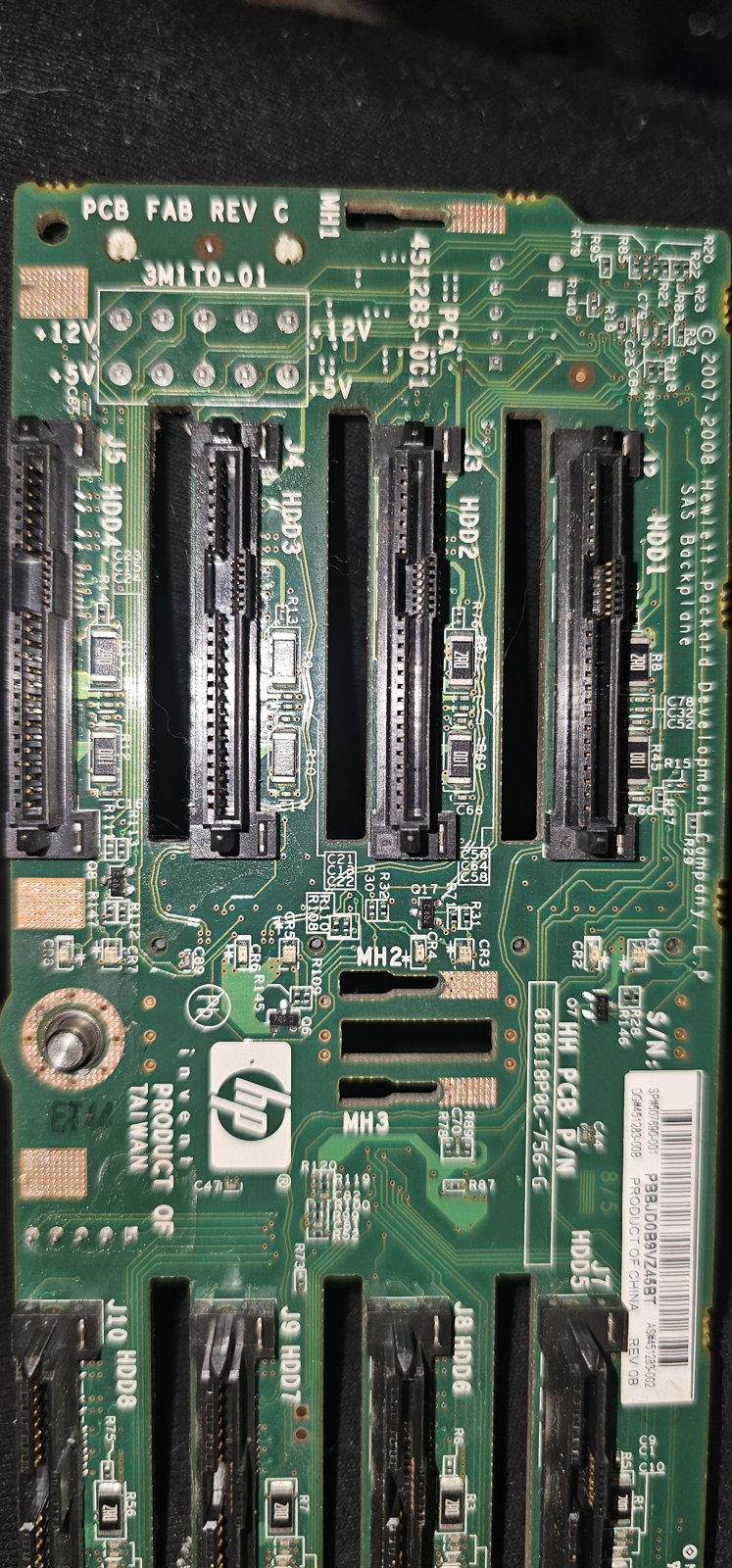
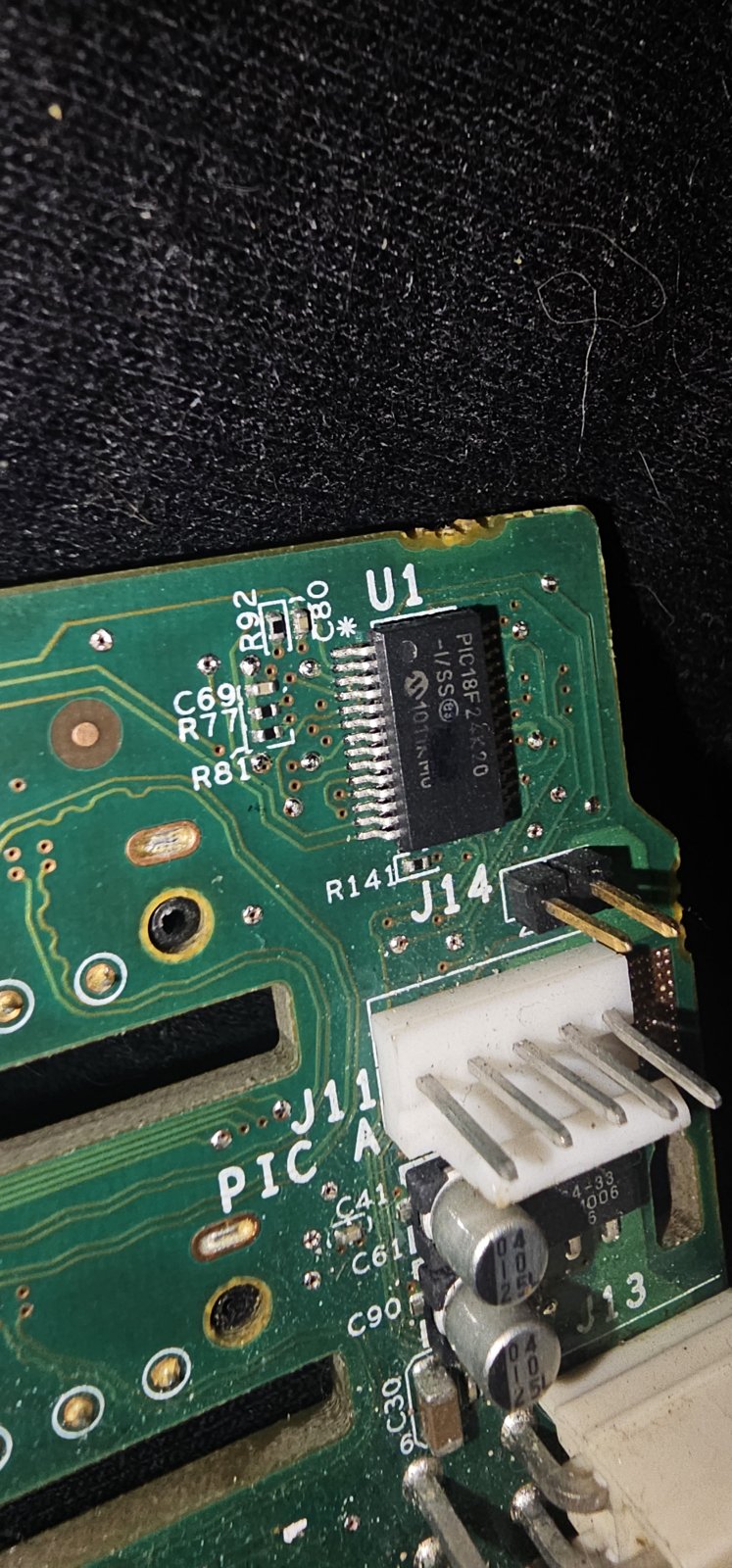
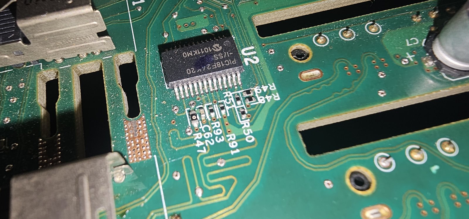
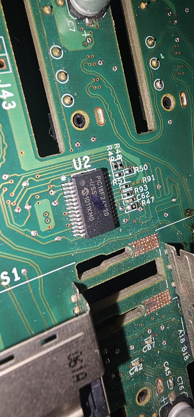
Each backplane has two PIC18F24K20 microcontrollers (28 pins, no crystal, running from their internal oscillator). PIC A looks after bays 1 to 4 and PIC B looks after bays 5 to 8. The 3.3 V rail comes from a small linear regulator, a TC1264-3.3 (800 mA, SOT-223, marked 1264-33 / VDB1006) fed from the 5 V pins of the power connector.
There is a 10-pin Mini-Fit Jr power connector (J13, the only Molex part on the board) that carries more than power: two of its pins are an I2C bus and another is an “address strap” analogue input. There are also a 3-pin I2C header (J44), two plain 0.1 inch 2-pin headers (J14 beside PIC A, and an unpopulated J43 beside PIC B), and two ICSP programming headers (J11 for PIC A and J12 for PIC B). The two SAS connectors are SFF-8087 types, J1 (silkscreen IPASS1) feeding PIC A and bays 1 to 4, and J6 (IPASS2) feeding PIC B and bays 5 to 8.
Reading the chips
I used a Microchip ICD 4 with MPLAB X’s command-line programmer. A few practical notes, since they cost me time:
- The ICD 4 does not power the target, so the backplane needs its own bench supply, and I ended up needing the 12 V rail connected as well.
- Pin 1 orientation on the ICSP header matters, and I got it wrong the first time.
- While the ICD 4 is attached it holds the PIC in reset. Unplug the lead to let it run.
- The programming lines are the same pins the PICs use to detect whether a drive is fitted in two of the bays, so pull any drives out of those bays before you programme.
The first good news was that neither chip is read protected. Before doing anything else I took a full backup of both chips (program memory, configuration bits, user ID and the little data EEPROM) and kept it somewhere safe. I’m not publishing the dumps, because it’s HP’s firmware, but I did compare them: the program code on the two chips is identical, and only the EEPROM differs, in a handful of bytes that tell each chip which half of the backplane it is.
Finding out what the firmware does
There’s no source, so I wrote a small PIC18 disassembler and read the start-up code. That gave me the list of which pins are outputs and which are inputs, and the rest followed from watching the board:
- Thirteen outputs: the LED pins, plus one that toggles constantly (I’ll come back to that).
- An I2C slave on the usual hardware pins.
- Two analogue inputs, and a handful of digital inputs.
The oddest discovery was how the chip decides its I2C address. It doesn’t use a fixed address or a jumper. It measures a voltage on one pin, averages four ADC readings, and uses the result to pick an address from a table. That voltage comes from pin 9 of the power connector. It goes straight to PIC A, and through a 750 Ω resistor to PIC B, with 5.6 kΩ to ground on each chip’s input. PIC B also reads a voltage with pin 9 grounded, which that network can’t produce on its own, so I think there is a pull-up on it that I haven’t found yet. With pin 9 floating, both chips answered at the same address and collided. Grounding pin 9 live, with the board running, moved them to two separate addresses and I could talk to each chip individually.
The protocol itself is a simple framed command set: a type byte, a length, a command and a checksum that is the two’s complement of the sum. Replies start with a status byte. The documented behaviour I found was a firmware version query, an LED self-test that chases through every LED in each bay, a command that lights the blue “locate” LEDs, and some housekeeping queries.
The mistake
One command in the stock firmware writes to the chip’s EEPROM. I sent it a few times with junk while trying to work out what it did, and the chip’s behaviour changed afterwards. I’d corrupted its configuration area. It was recoverable only because I had backed everything up first.
The restore itself taught me something worth passing on: with Microchip’s ipecmd, the option that programs only the EEPROM (-ME) also erases the flash and resets the configuration bits. The safe way to restore is to programme the whole original hex file with the plain programme option and then read everything back and compare. I did that, and the round trip came back byte-for-byte identical.
The lesson is the usual one: back up first, and don’t send commands you don’t understand to firmware you can’t easily reflash.
Mapping the LEDs and the presence pins
Each bay has three LEDs and one “is a drive fitted” input. I found them by lighting one pin at a time and watching, and by hot-swapping drives while reading the port registers. All of the LED pins are active low (pulling the pin low lights the LED), and the drive-detect pins are active low too.
| Bay (PIC A / PIC B) | Blue (locate) | Green (activity) | Amber (error) | Drive detect |
|---|---|---|---|---|
| 1 / 5 | RA2 (pin 4) | RA4 (pin 6) | RC2 (pin 13) | RA7 (pin 9) |
| 2 / 6 | RA3 (pin 5) | RA5 (pin 7) | RB3 (pin 24) | RA6 (pin 10) |
| 3 / 7 | RB5 (pin 26) | RC0 (pin 11) | RC7 (pin 18) | RB7 (pin 28) |
| 4 / 8 | RB4 (pin 25) | RC1 (pin 12) | RC6 (pin 17) | RB6 (pin 27) |
Drive detect turned out to be neat. Pin 5 of each drive’s power connector (a ground pin on the drive side) goes through a 330 Ω resistor to the PIC’s detect pin, and the pin sits at about 7.5 to 10 kΩ to ground with no drive fitted, so a pull-up is implied. Fit a drive and its ground pulls the pin low. All eight bays are the same.
One thing I want to be clear about: drive activity is not wired to any input on the PICs. A drive with no data link never changed any pin apart from insert and remove. Early on I wrongly concluded that the PICs couldn’t see drives at all, from a run where I hadn’t actually moved the drive, and I invented a theory to explain it. I retracted both when I realised. Bad science on my part, and I’m glad I caught it.
Replacing the firmware
I wrote a replacement in C for the XC8 compiler. It is an I2C slave with a pointer-and-auto-increment register map, so a host can set a colour mask for each LED group, read the raw port pins (which tells you which bays have drives fitted), read the two ADC channels, and, for debugging, take direct control of the port latches. The two chips of one backplane get consecutive addresses (0x30 and 0x31 on the first, 0x32 and 0x33 on the second), set at build time. I flashed all four chips across the two backplanes, verified each byte for byte, and ran a slow colour twinkle across both as a test. The original images remain restorable.
The host side started life as an ESP32 acting as an I2C master. It has since been replaced by a Raspberry Pi Pico 2, which also runs the fans and the front panel; that is the second half of this post. On the first cage the register interface works end to end (colour masks, drive-detect and the ADC channels). The chips on the second cage are flashed and verified, but I haven’t exercised their registers yet.
The side channel: SGPIO
The weird output that toggles constantly bothered me. In the stock firmware, one interrupt handler on a single input pin runs a long state machine that alternates between sampling one input and driving that output. Four pins, one clock, one load strobe, one data in and one data out. That is exactly the shape of SGPIO (SFF-8485), the serial bus a SAS controller uses to tell a backplane which LEDs to light.
The decoded behaviour per bay is three bits each way. From the controller, the three bits drive the green activity, blue locate and amber error LEDs. Back to the controller, the chip reports drive presence. That also explains why the stock I2C interface only exposes the blue LED: green and amber were meant to come from the HBA.
The pin mapping, which I confirmed with a meter:
| PIC pin | Role | SFF-8087 pin on J1 / J6 | Verified how |
|---|---|---|---|
| 23 (RB2) | SClock | A8 (SB0) | matched-length trace pair seen, not buzzed (the row is hidden under the connector) |
| 21 (RB0) | SLoad | A9 (SB1) | same matched pair |
| 22 (RB1) | SDataOut | B10 (SB4) | buzzed |
| 16 (RC5) | SDataIn | B11 (SB5) | buzzed |
The standard sideband assignment for these connectors comes from a 2007 T10 document, and the pins I could reach (B row) matched it exactly: B7, B9 and B12 are ground, B10 goes to pin 22 and B11 goes to pin 16. The A row sits underneath the surface-mount connector body where I couldn’t get a probe in, but the two lines that I couldn’t reach arrive as a length-matched pair at PIC pins 23 and 21, which fits a clock and a strobe.
Does it work with my HBAs? I don’t know. The cards are LSI 9211-8i (SAS2008), and reports of whether those drive the sideband in IT mode are mixed. I’ve built a passive capture mode for the replacement firmware that counts clock edges and records raw samples over I2C, so the first test will be a definite yes or no. It isn’t flashed yet.
The LED circuit
Then I started tracing the LED network by hand, with the board powered down, measuring resistance and diode drops in circuit. This is the awkward part: much of the board is hidden under surface-mount parts and I only managed one bay properly.
- Green and amber: the anode goes to the 3.3 V net, and the cathode goes through a 68 Ω resistor straight to the PIC pin. That is about 19 mA per LED, comfortably inside the PIC’s limit.
- Blue: the anode goes directly to the 5 V rail. The cathode goes through a 120 Ω resistor to the drain of a small SOT-23 N-channel MOSFET. The source of that MOSFET goes straight to the PIC pin, and its gate is tied permanently to 3.3 V.
That FET is a nice little piece of design. A blue LED needs about 3 V, which a 3.3 V supply can barely give, so HP runs it from 5 V. But a 3.3 V microcontroller pin must not see 5 V. With the gate held at 3.3 V, the transistor conducts when the PIC pulls its pin low (lighting the LED) and switches off when the pin is high, so the 5 V side never reaches the chip. There are eight of them, one per blue LED: Q7, Q17, Q6, Q8, Q3, Q9, Q4 and Q5 for bays 1 to 8. Each bay also has a dual LED (CR1, CR3, CR5 and so on) and a separate green one (CR2, CR4, CR6 and so on). The part is marked 701 on mine, while the ON Semiconductor 2N7002L datasheet lists the marking as 702, so I’m treating it as a 2N7002L-class device until I find out otherwise.
There are also two 100 µF electrolytic capacitors by every drive connector, one on the 5 V rail and one on the 12 V rail.
I’ve only measured bay 1 on PIC A. The rest of the board is drawn on the schematic as assumed identical (amber and dashed) rather than measured, and I’d rather the drawing said so than pretended otherwise.
The schematic
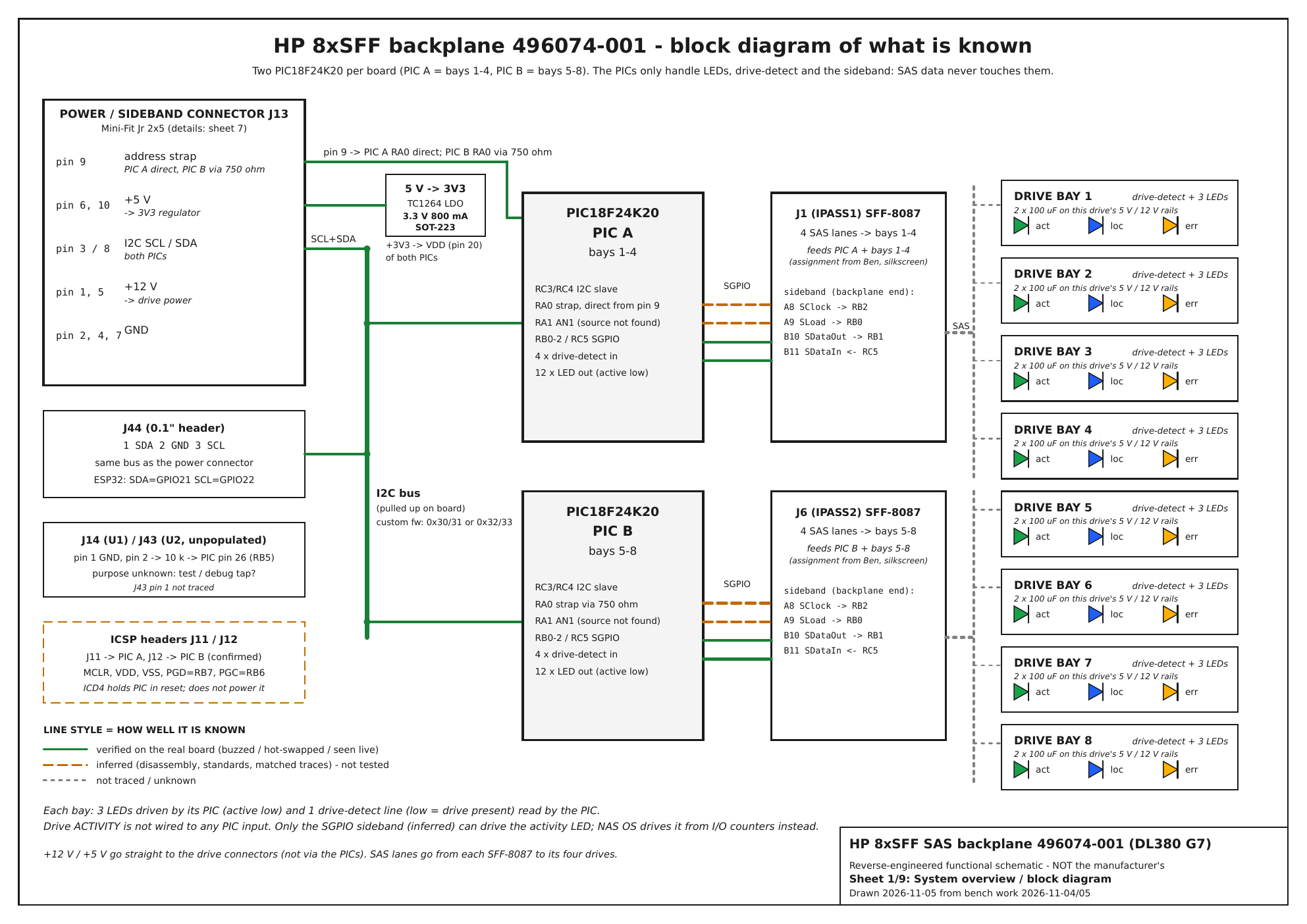
I generate the drawing from a script, so it can be corrected as I trace more of the board. There are nine A3 sheets in the PDF. The first is the block diagram above, the next three are the wired component-level schematics, and the remaining sheets are the pin maps, the connector pinouts, the per-bay table and the firmware interface.
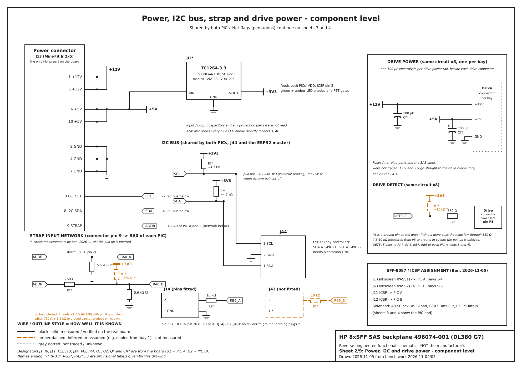
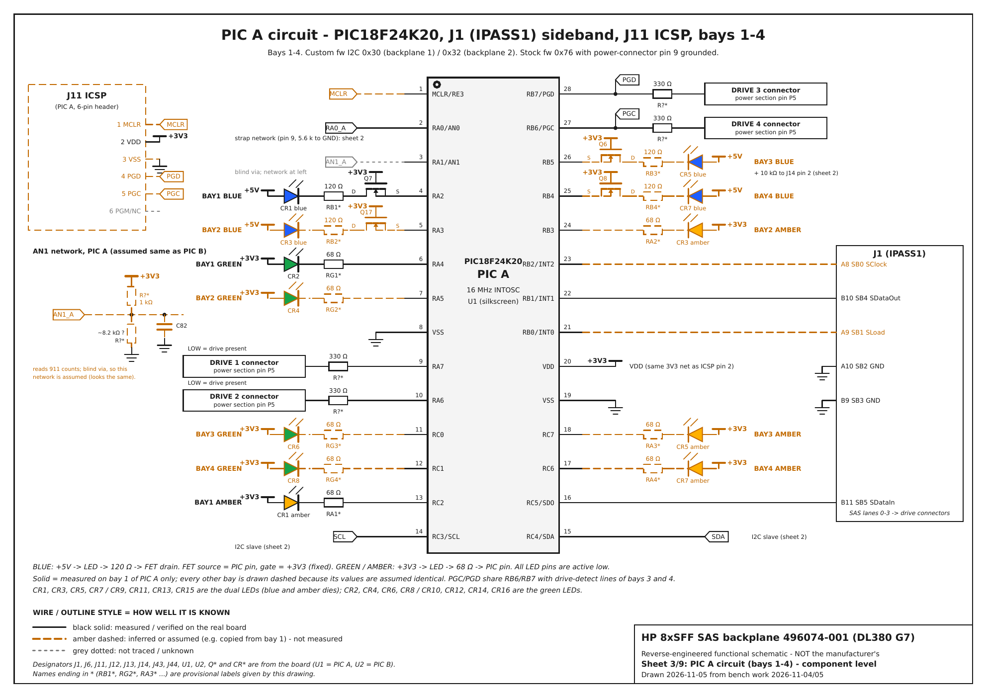
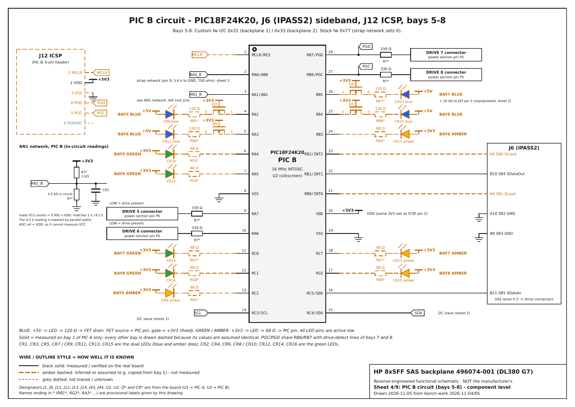
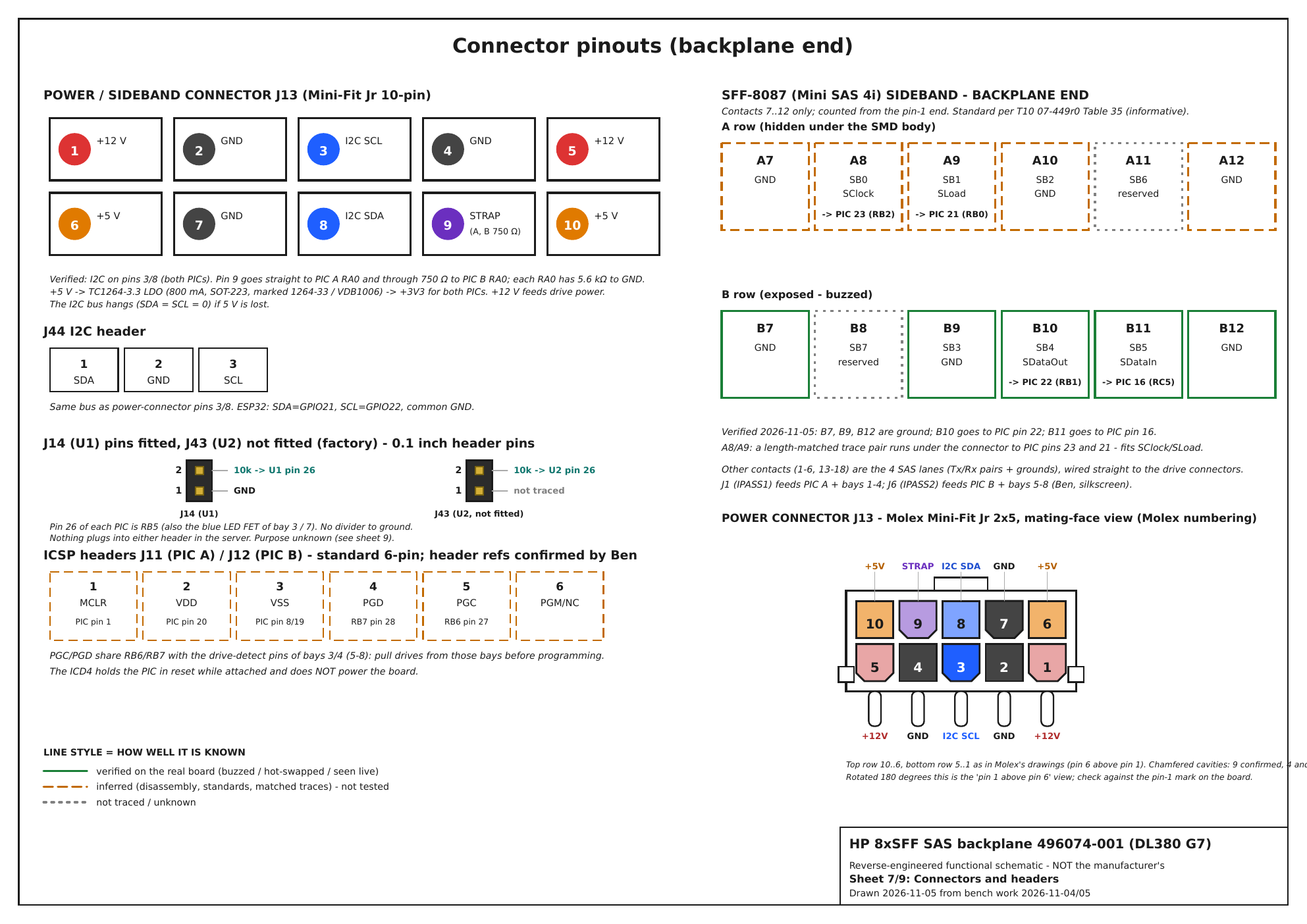
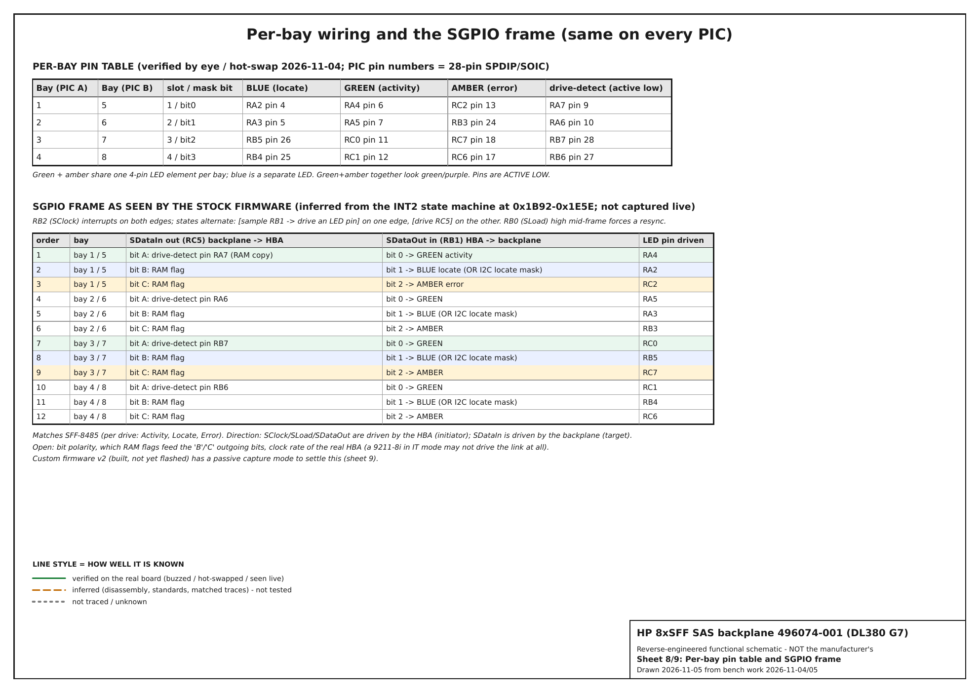
Reading it is straightforward: black solid lines are measured, amber dashed lines are inferred, and grey dotted lines have not been traced. The reference designators J1, J6, J11, J12, J14 and J44 come from the board’s silkscreen. Anything with an asterisk, like Q1*, RB1* or DG2*, is a name I invented to keep the drawing readable.
The PDF is at the end of the post.
Controlling it all: from an ESP32 to a Pico 2
The backplanes now speak a simple I2C register protocol, but something has to talk to them, and the same something has to run four case fans, read temperature probes and press the server’s power button. I started with an ESP32, then realised I had Raspberry Pi Pico 2 boards on the shelf and no WiFi requirement, so the controller is now a plain Pico 2 that plugs into a spare internal USB header on the motherboard. USB powers it and carries all the traffic: status, configuration, alerts and firmware updates.
What hangs off it:
- I2C to the two backplanes (the J44 headers), which gives the NAS control of every bay LED.
- Four PWM fans with tach, each through one 2N3904 that pulls the PWM line low (open collector), so it works with any fan pull-up. A jumper decides what the fans do if the Pico is off or hung: they go to full speed.
- A 1-Wire bus for DS18B20 temperature probes.
- Power and reset: two transistors across the front-panel header pins, in parallel with the real buttons, plus drivers for the 12 V LED rings in the case buttons and sensing of the motherboard’s own power and drive-activity LED signals.
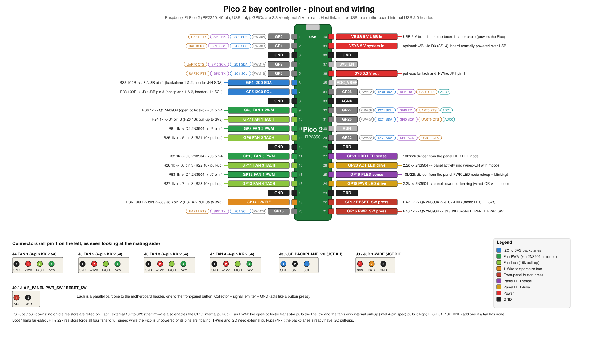
A few design decisions that are worth passing on:
- I don’t rely on the RP2350’s internal pull resistors. The A2 stepping has a known erratum that makes the pull-downs unreliable, and pull-ups are weak for a fan tach anyway, so the tach lines have a real 10 kΩ and the 1-Wire bus a real 4.7 kΩ.
- I swapped some pins from my first plan so that fan PWM and tach pins alternate. That makes the wiring to each fan header run straight across instead of crossing, which matters when you are building it on stripboard.
- The fan headers are stacked in one column, so the four 12 V pins (and the four grounds) can be joined by a heavy wire under the board.
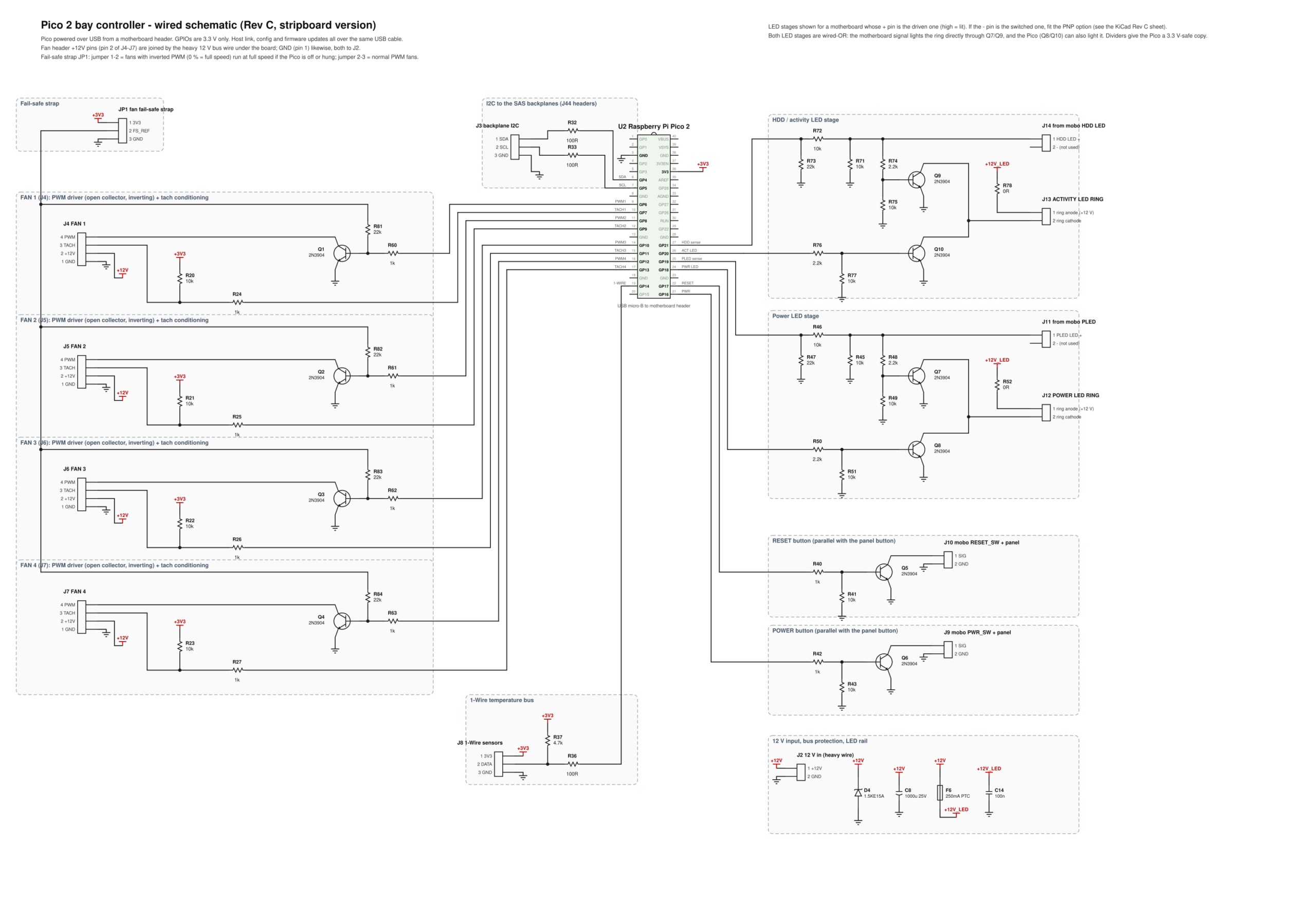
I generated the drawing from a script and checked it electrically: it knows the intended connections, and it fails if any wire shorts two nets, leaves one open or crosses another. A stripboard layout then came out of the stripboard-editor.com solver at 31 by 49 holes, after a couple of attempts. None of this has been built yet, so treat it as a design, not a tested board.
Fans that learn
The Pico runs the fans itself, so they keep working if the NAS is off or crashed. Each fan has a temperature curve of up to eight points, hysteresis so it doesn’t hunt, and slew limiting so it doesn’t lurch. Three temperatures matter: a target the fan should settle at, a limit above which it adds 10 per cent per degree on top of the curve, and a critical temperature at which it goes to full speed.
On top of the curve there is a learned correction. Every thirty seconds, if the zone is warmer than the target, the correction for the current temperature band (2 °C wide) goes up a step; if it is comfortably cooler, it goes down. Over hours the fan finds the quietest speed that holds the target, band by band. It is saved to flash at most every fifteen minutes, so the flash isn’t worn out.
Calibration measures each fan’s start speed and its RPM at every speed, and it also tests the polarity. Fans differ: some run faster at a low PWM duty (inverted). It runs the fan at 20 per cent and then 80 per cent, and if the fan is faster at 20 it flips the software invert flag for that fan.
When a fan dies
A fan that is being driven but sends no tach pulses for eight seconds is treated as failed. Most servers respond by sending every other fan to full power, which is loud. I wanted something calmer: fans are grouped by what they cool, and when one fails the healthy fans in the group are raised by the ratio of total to healthy (so with four fans and one failed, the others go up by a third), capped at 85 per cent by default. Learning pauses while they are covering, so the learned curve isn’t polluted. A critical temperature still means full speed.
The Pico also notices a fan that is turning, but far too slowly (under half its calibrated speed for thirty seconds) and reports it. Every change of state goes into a numbered ring of events and is sent to the NAS straight away, so a host that was busy can still ask for what it missed.
NAS//OS: the control panel
The NAS operating system I’m writing is the control panel for all this. You create zones: a zone is a set of fans plus whatever they cool, drives by cage or bay and temperature probes by their unique ID. The NAS sends the Pico the hottest drive temperature in each zone from SMART, and keeps the Pico’s configuration in step with the zones by comparing what it reads back, so a Pico that has lost its settings is put right on the next poll. Failed fans, slow fans, a zone above its limit, a missing probe or a lost link raise an e-mail alert, and the alert clears when the problem does.
Telling the probes apart is the awkward bit with 1-Wire, because they are identical. The NAS has a “find a probe” button: it remembers every probe’s temperature, you warm one in your hand, and the one that heats up is highlighted so you can name it and say where it sits.
I was caught out on one thing: I’d written my own 1-Wire routines, JSON writer and checksum in the Pico firmware. Then I looked at what the ecosystem already provides and replaced them with the OneWire, DallasTemperature, ArduinoJson and CRC32 libraries. It’s less code to maintain and far less to get wrong.
It has been tested against simulations, not hardware: unit tests on the control logic (failure cover, limits, polarity detection), a whole-firmware simulation on the PC with a model fan and a thermal model, and 38 checks of the NAS side against a simulated Pico. The real test starts when I build the board.
What I still don’t know
- Whether my 9211-8i cards drive the SGPIO lines at all (test pending).
- The pad-level confirmation of the sideband clock and load pins (hidden row).
- Where the SAS lanes go (they bypass the PICs).
- The LED network on every bay except the first.
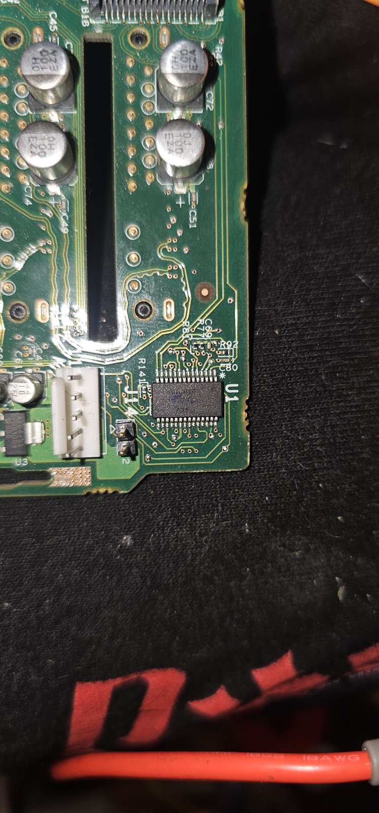
- What J14 and J43 are for. Pin 1 is ground and pin 2 goes through a 10 kΩ resistor to pin 26 (RB5) of the nearest PIC, with no divider to ground. That pin is also the blue LED output for bay 3 (bay 7 on the second chip), which makes me suspect a factory test tap, but I haven’t proved it.
- What the PICs’ analogue input RA1 is for. On the second chip it is a 1 kΩ and roughly 8.2 kΩ divider with a capacitor, reading a constant 0.891 of the supply, and on the first chip the trace vanishes down a blind via. My guess is a fixed hardware-ID strap, a bit like the address strap, but I haven’t proved it.
- Pull-up values, the regulator’s capacitors and the PIC B strap divider.
- How the Pico controller behaves on real hardware: the board is not built yet, and I haven’t run the 1-Wire library against a real probe on the RP2350.
What I’d do differently
- Back up the chips before touching anything, and verify the backup by reading it back.
- Don’t experiment with write commands on the only copy of the firmware.
- Check that I have actually changed the physical state before drawing conclusions from a log.
- Draw the schematic as you go. Doing it properly exposed a couple of places where I’d misattributed a connection in my notes, such as putting the interrupt on the wrong pin and the FETs on the wrong LED colour.
I’ll follow this up when the SGPIO capture test is done, when I’ve been through the rest of the bays with a meter, and when the controller board has been built and has met a real fan failure.
Downloads
- Reverse-engineered backplane schematic (PDF, 9 sheets): HP_8xSFF_backplane_reverse_engineered_schematic.pdf
- Pico bay controller schematic (PDF, wired): Pico2_bay_controller_wired_schematic.pdf
- Datasheets: TC1264, PIC18F24K20, 2N7002L (via WP Download Manager as usual).