Since I do a lot of camping, and several festivals per year (when there isn’t a pandemic on!), I identified the need for a proper fridge that can be powered from my solar setup. Such fridges & coolers already exist, that run from either mains AC, 12/24v DC, and some of them (absorption cycle) will run from bottled gas.
The last option is out, as they’re hideously inefficient, and this would require the carrying around of a flammable gas source. Ready-made units using the vapour-compression method used in all domestic & industrial refrigeration, but they are very expensive. For an upright fridge type unit that could store enough to feed a family of 4, I was looking at over £550+VAT. A cheaper option was definitely required.
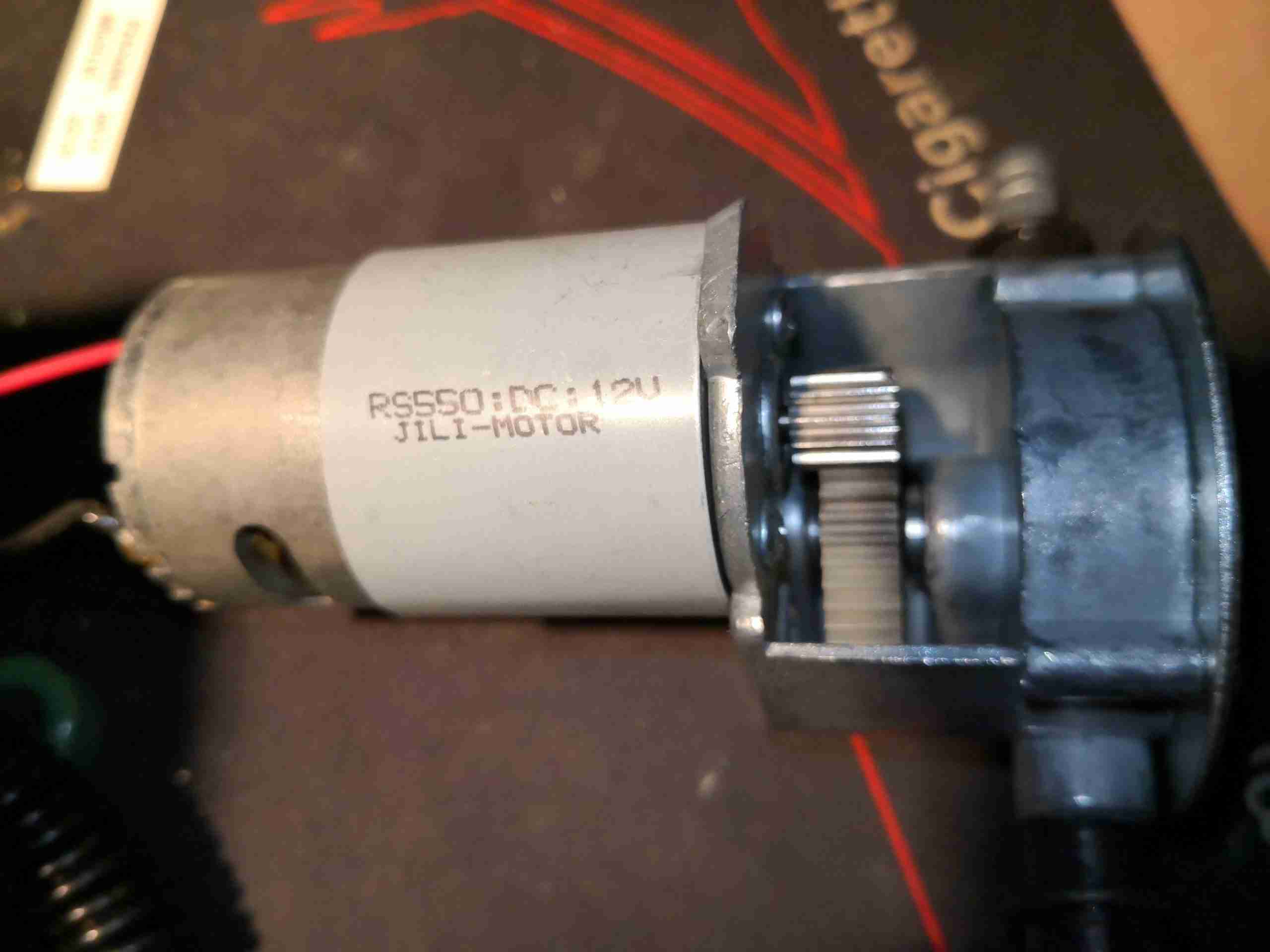
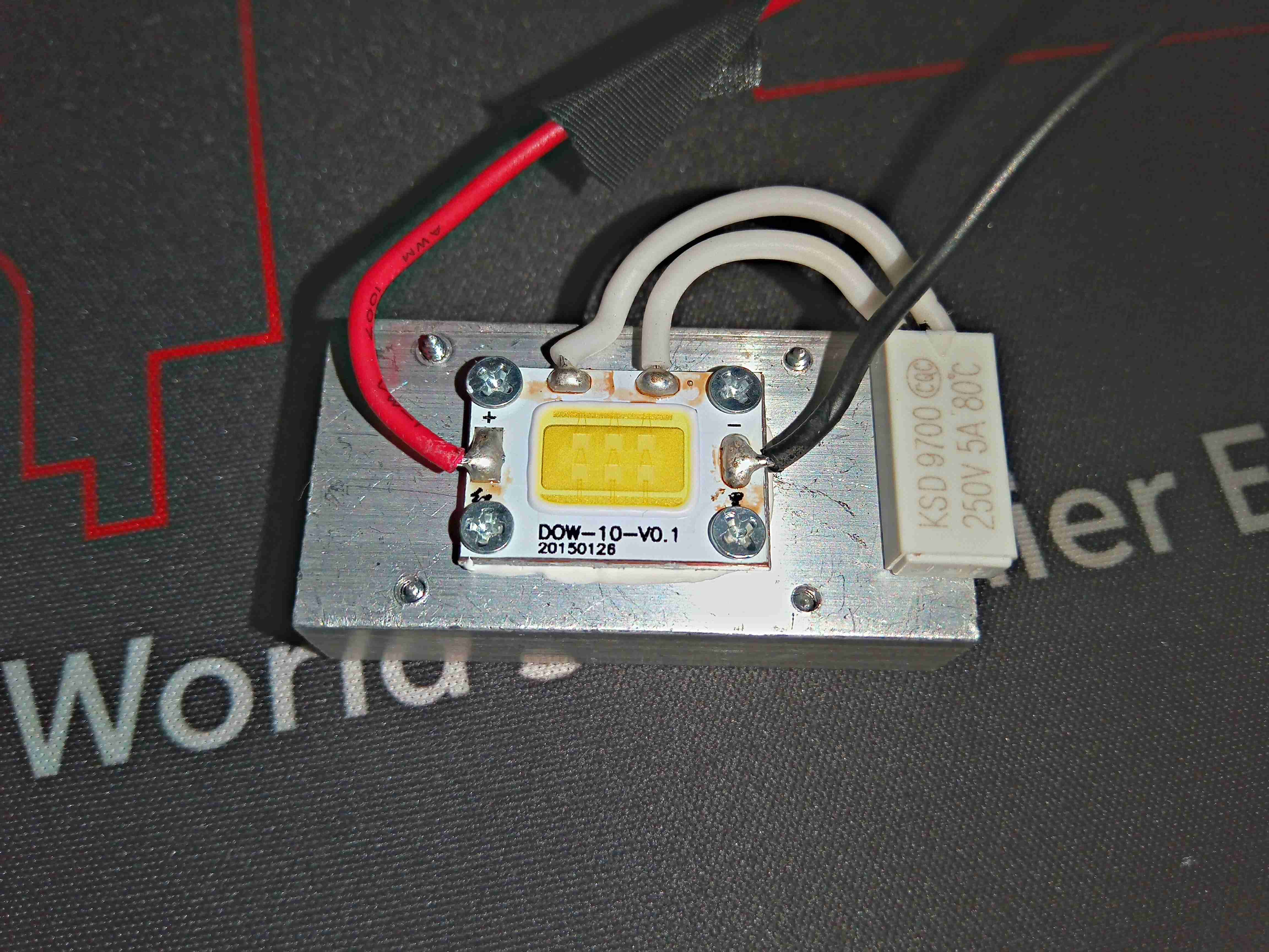
Since I already have a couple of spare Danfoss BD35 DC refrigeration compressors, I decided to grab a cheap domestic mini-fridge, and perform a compressor-ectomy to make the unit operable on a low voltage supply.
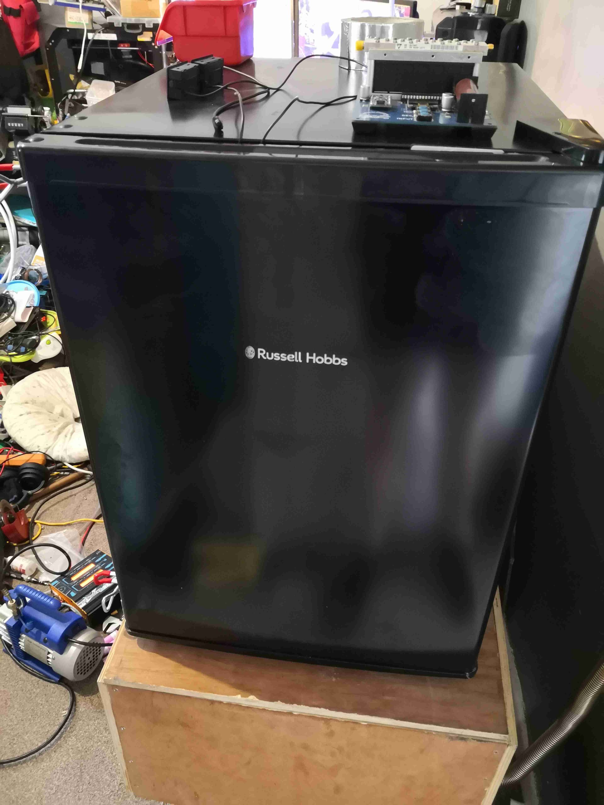
Russel Hobbs Mini-Fridge
Here’s the fridge I obtained from one of the many suppliers of domestic kit, this is a Russel Hobbs branded mini-fridge.
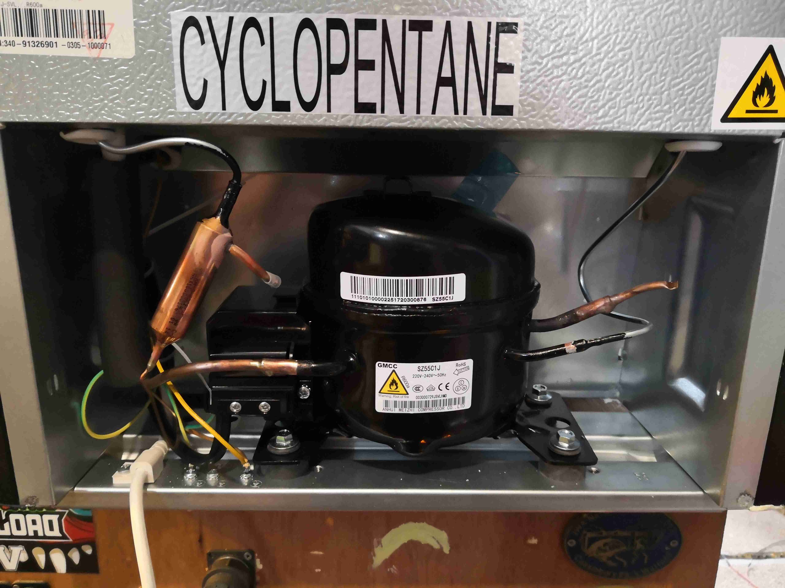
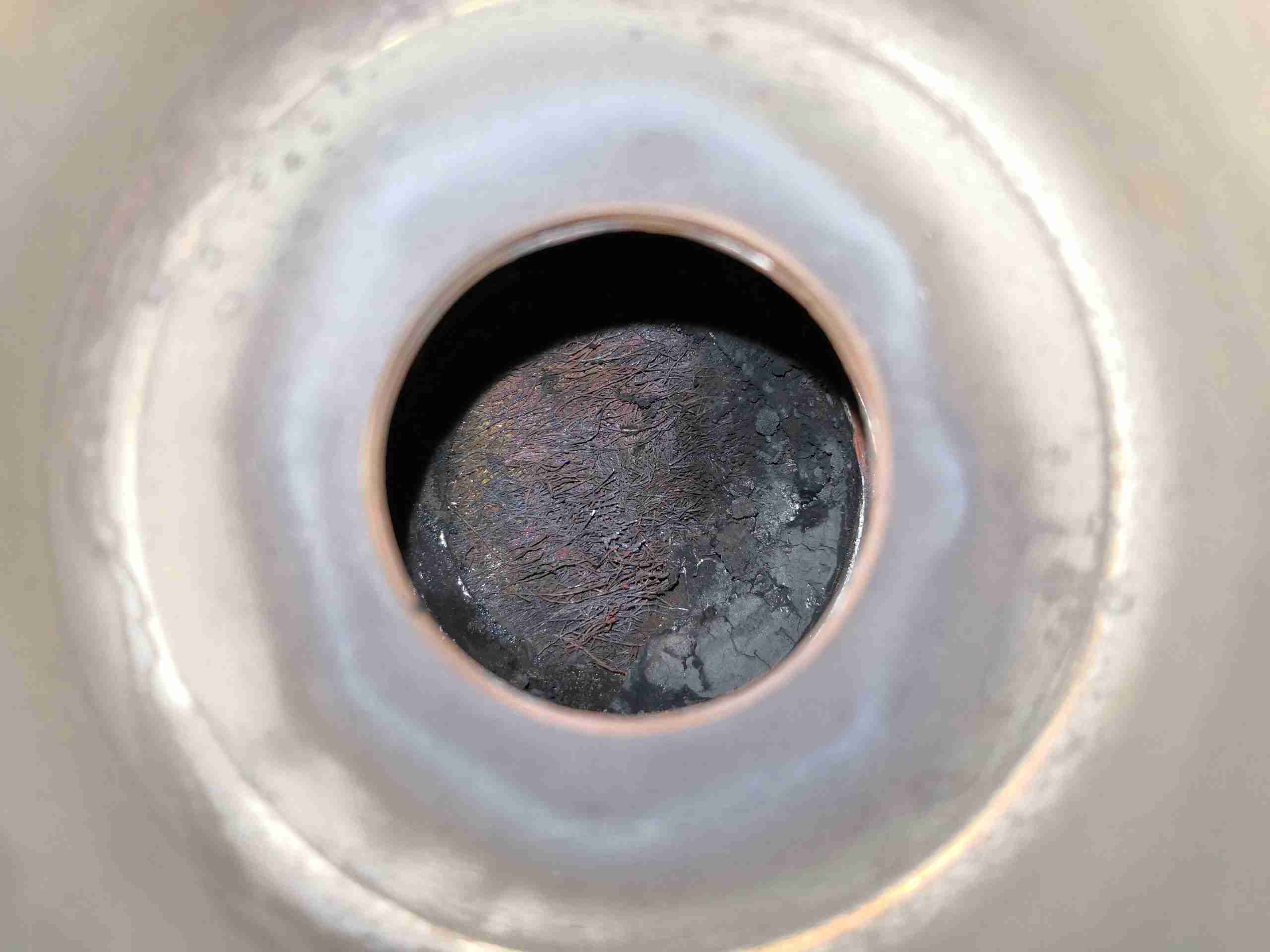
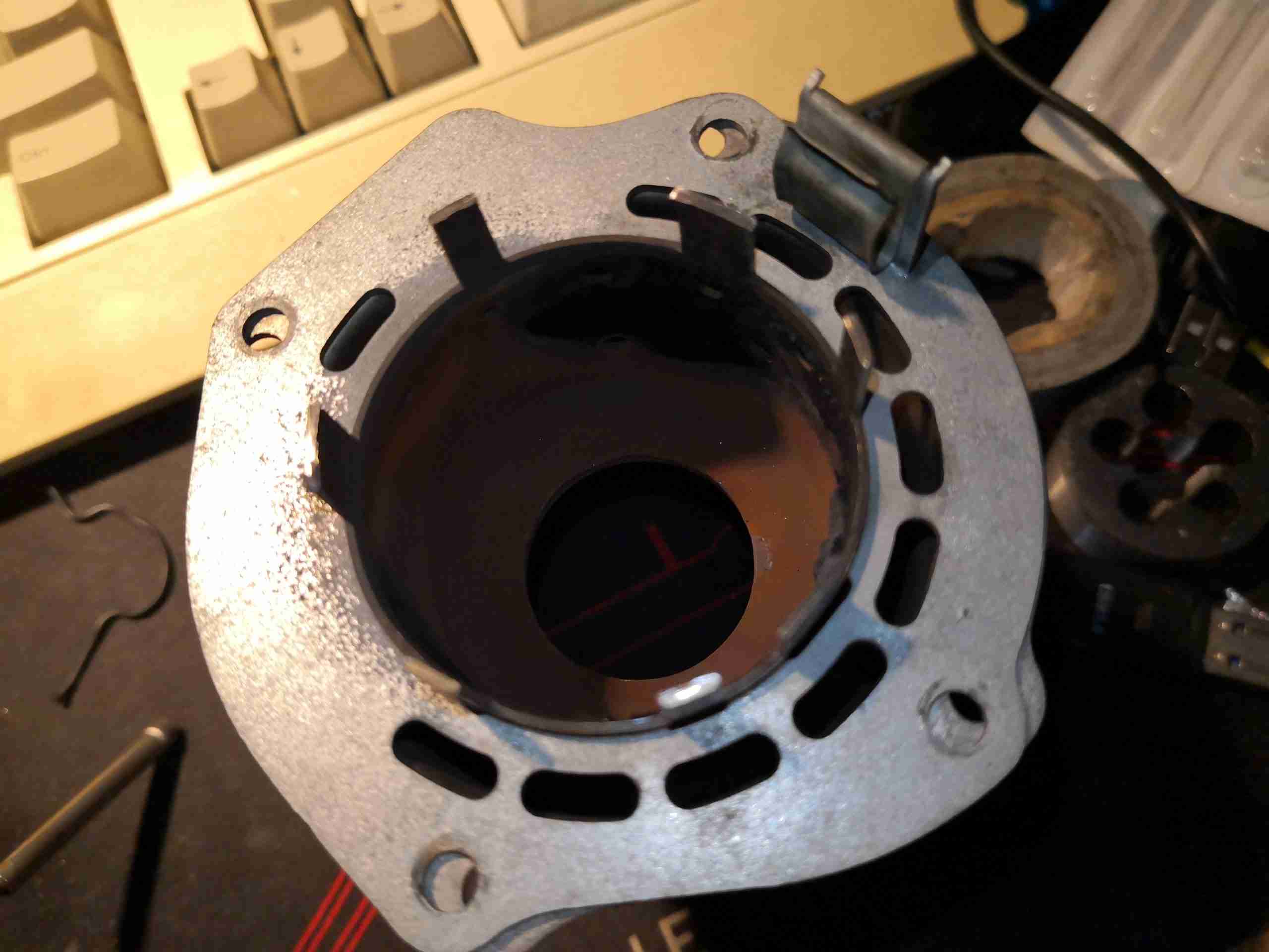
Factory Compressor
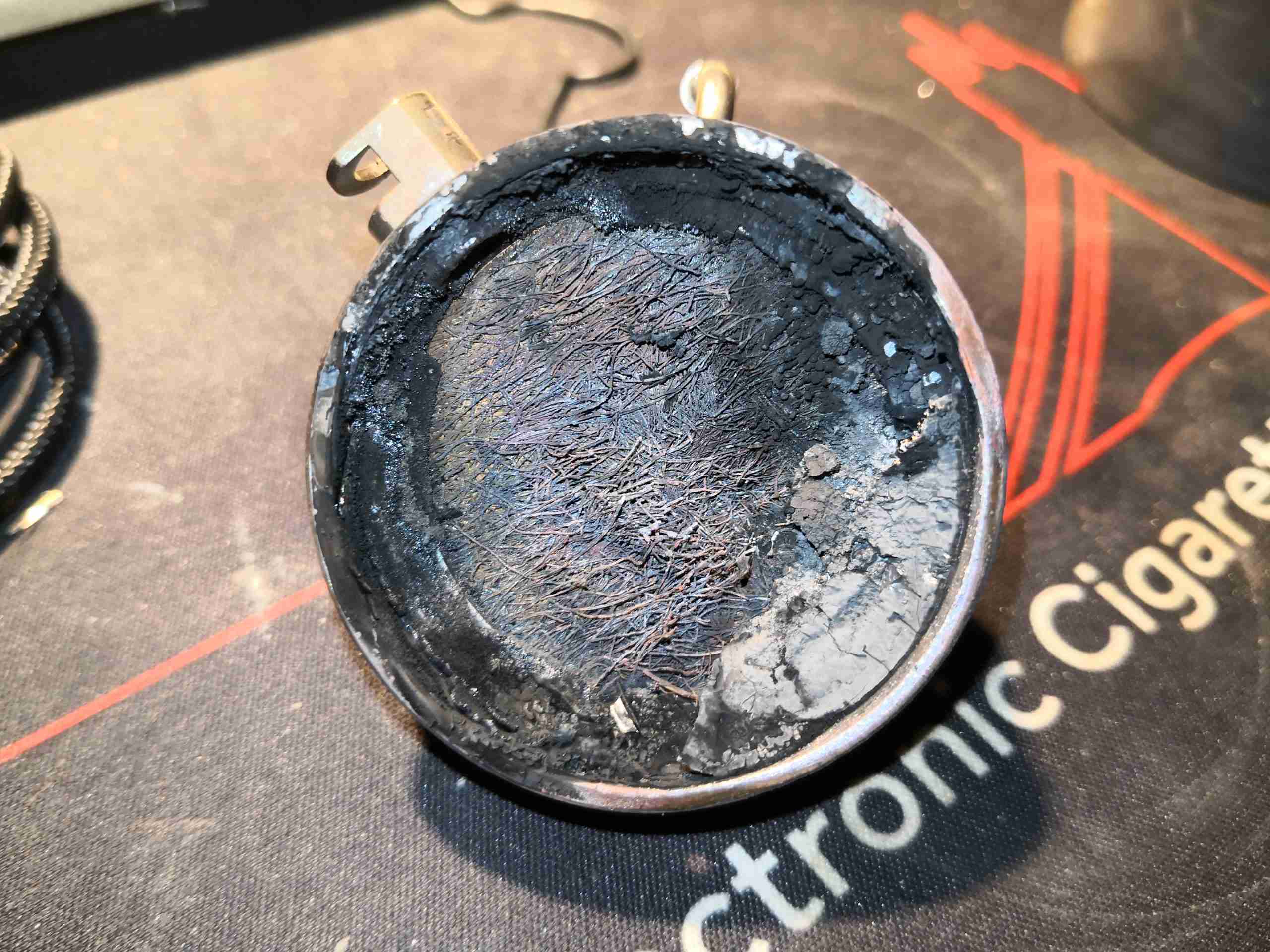
I was careful to select a unit with no Aluminium pipework – the stuff is damn near impossible to join onto with soldering. Brazing is impossible due to the temperatures involved. These units have copper & steel in their circuit, so this will be easy. Factory charge is 16g of R600a (Isobutane). This one isn’t even going to make it to the point of being plugged in before modification!
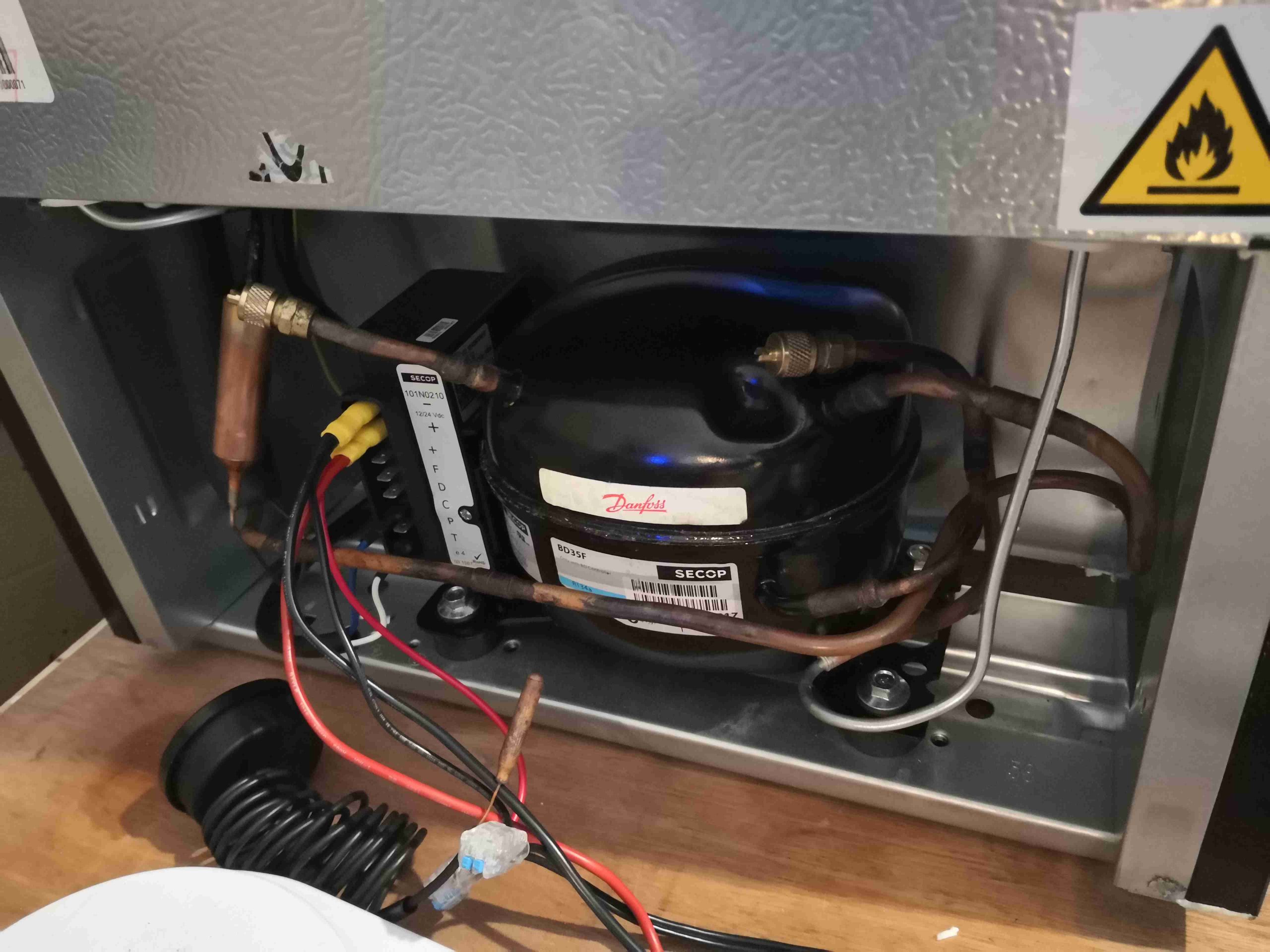
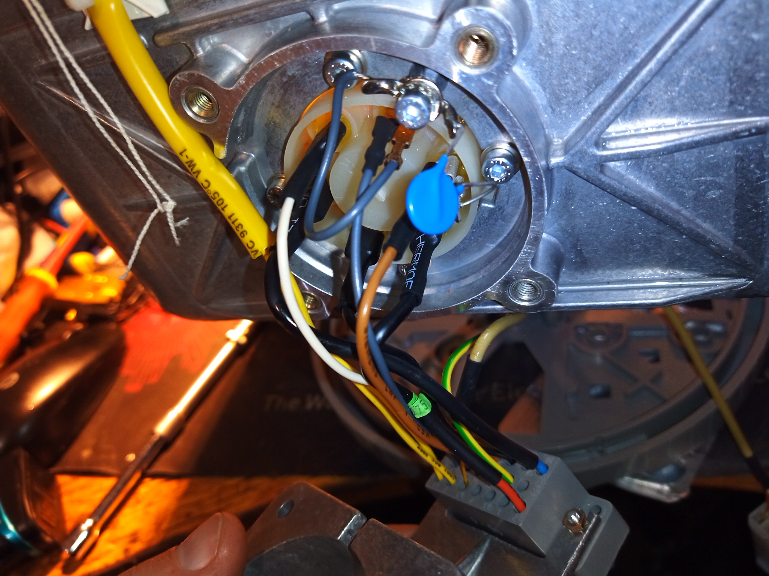
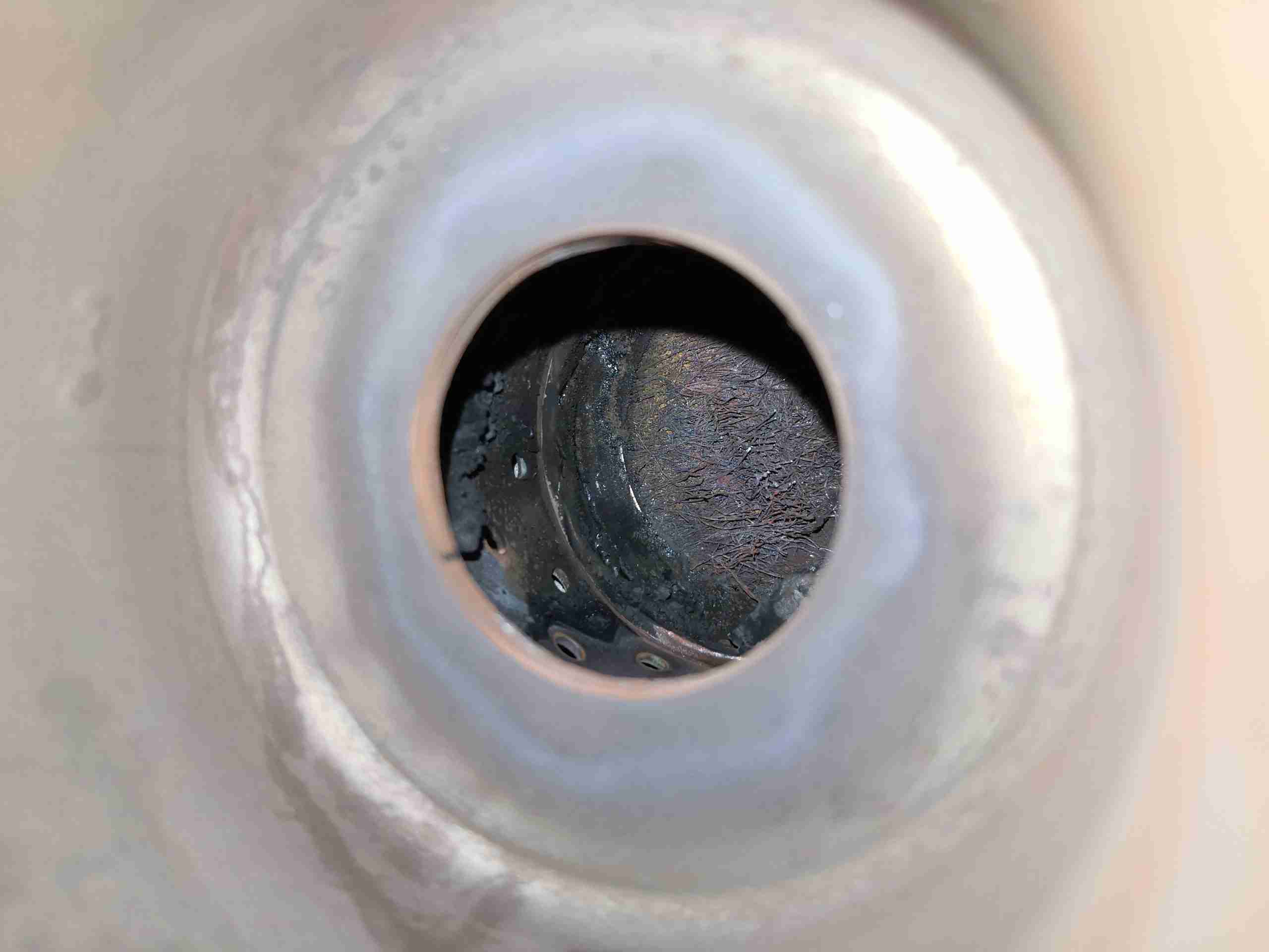
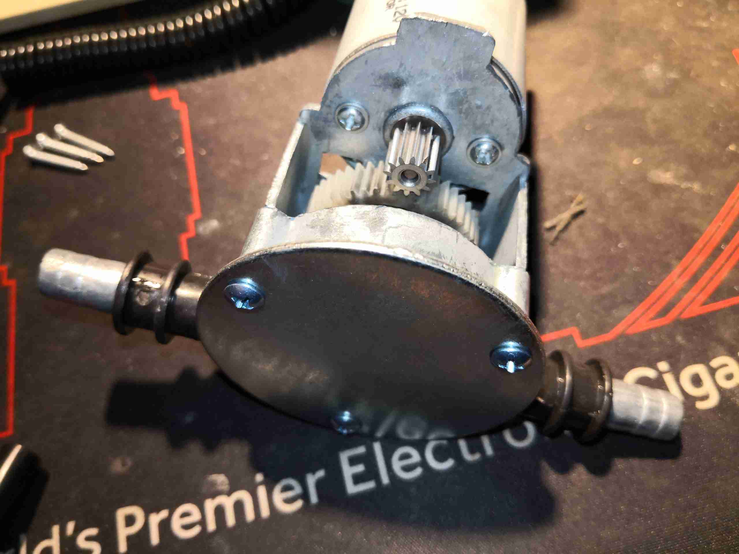
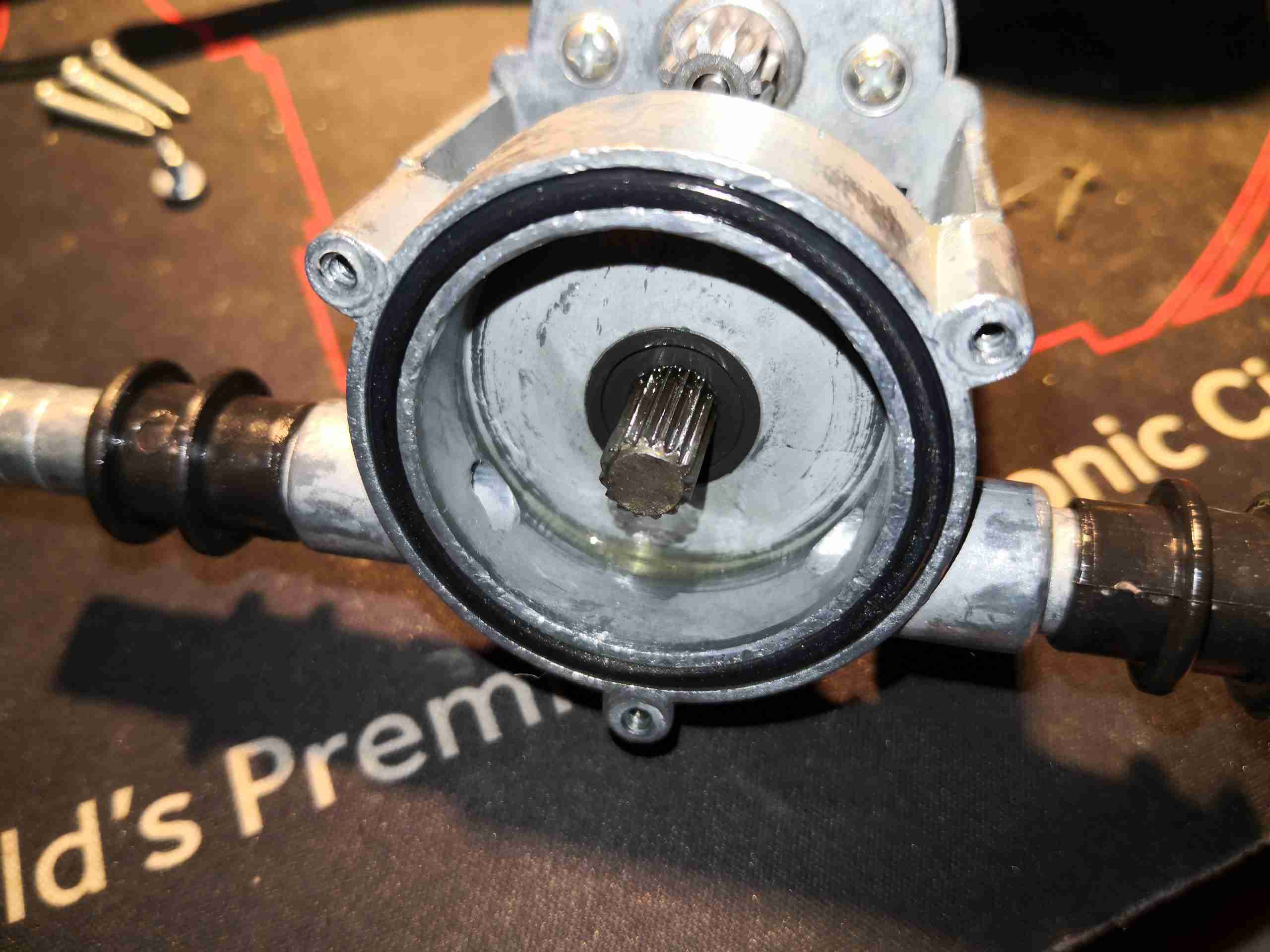
BD35 Fitted
I evacuated the factory charge, and removed the original compressor. To avoid having to disturb the capillary tube, I ensured the system was in continual nitrogen purge to keep moisture out – this meant I could retain the factory filter-drier. The condenser in this fridge is skin-type, on both sides of the outer shell, and formed from steel tube. This connection required the use of silver braze to connect to the compressor.
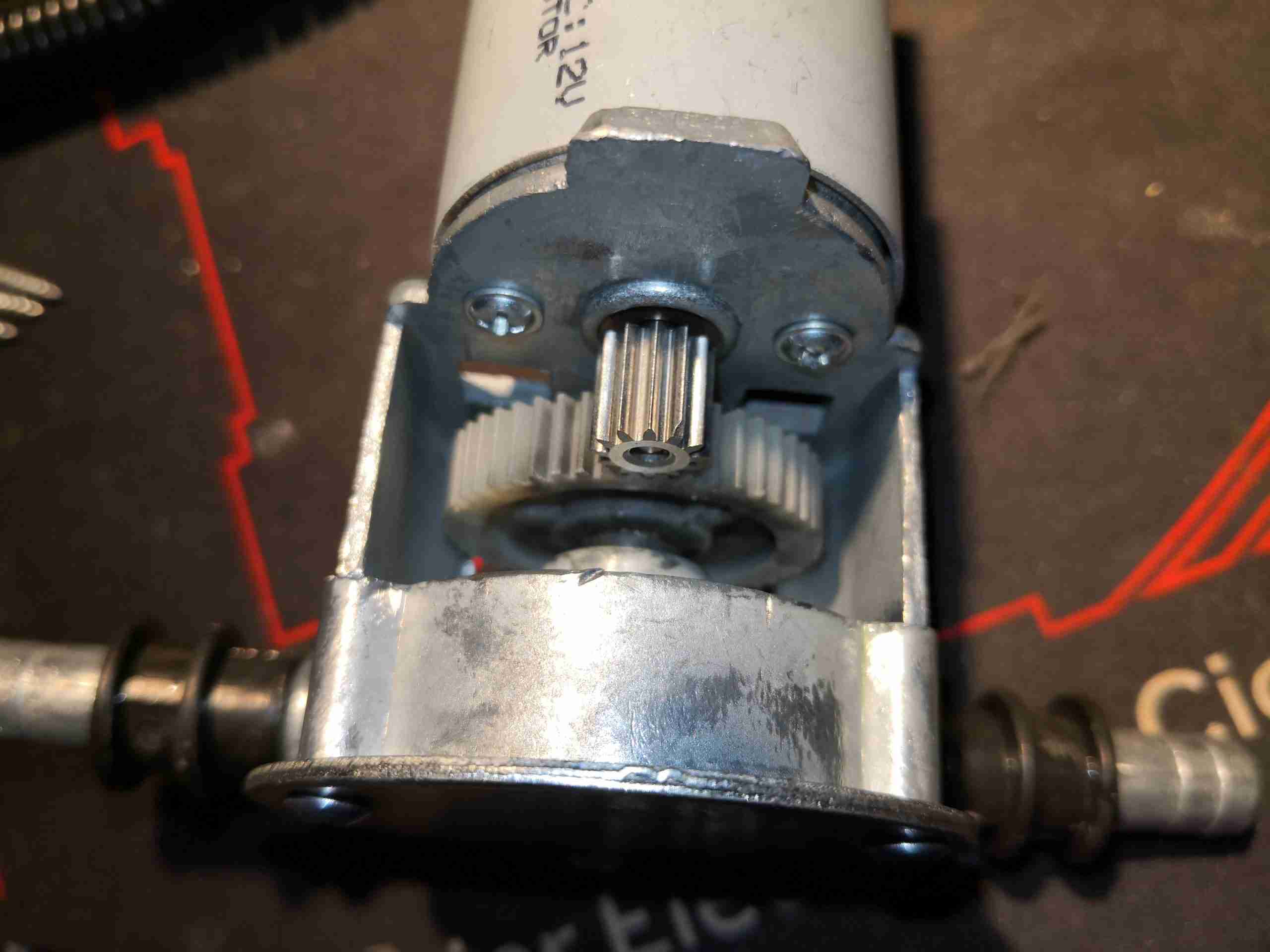
The suction line from the evaporator is copper, so that’s an easy braze onto an extension to the compressor.
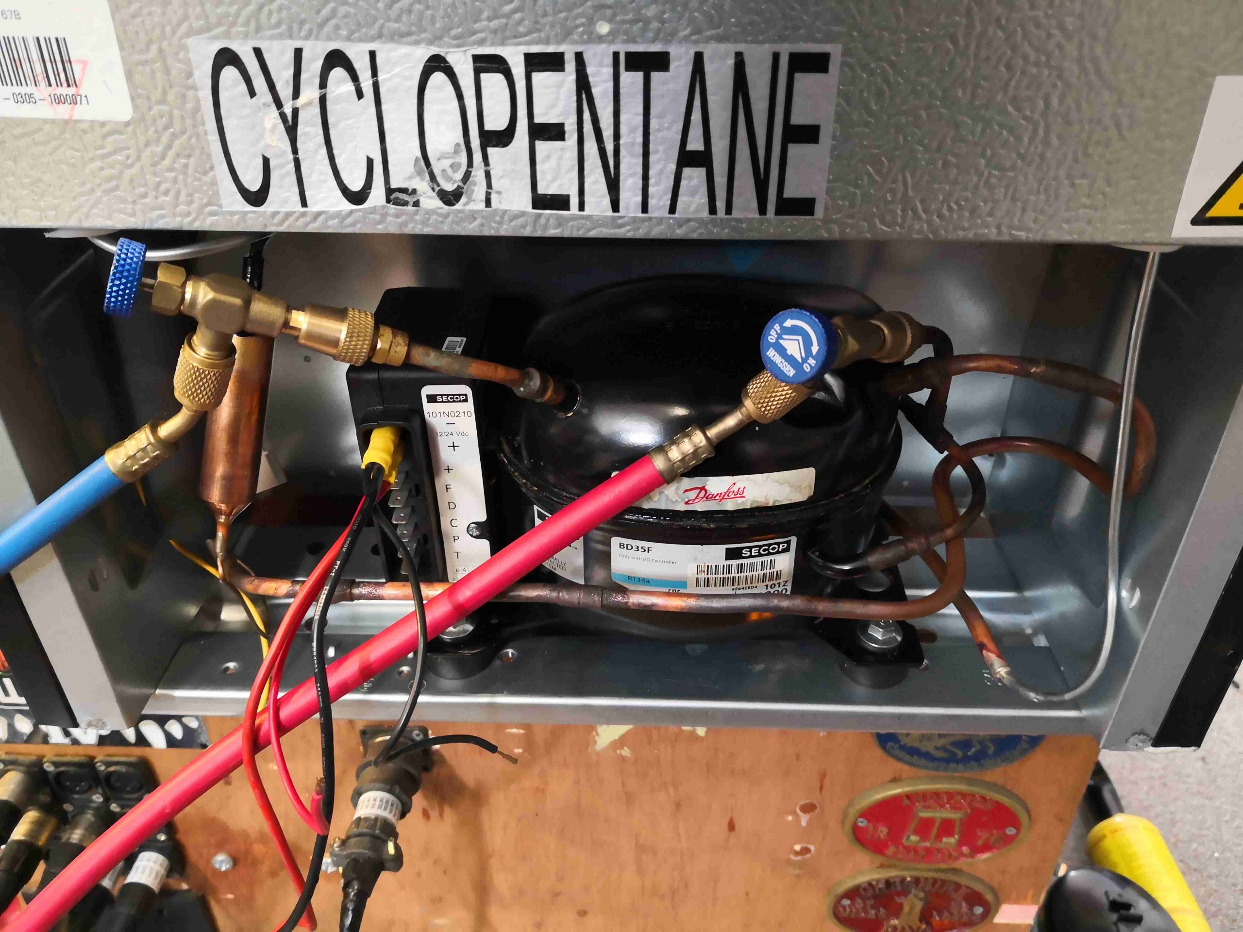
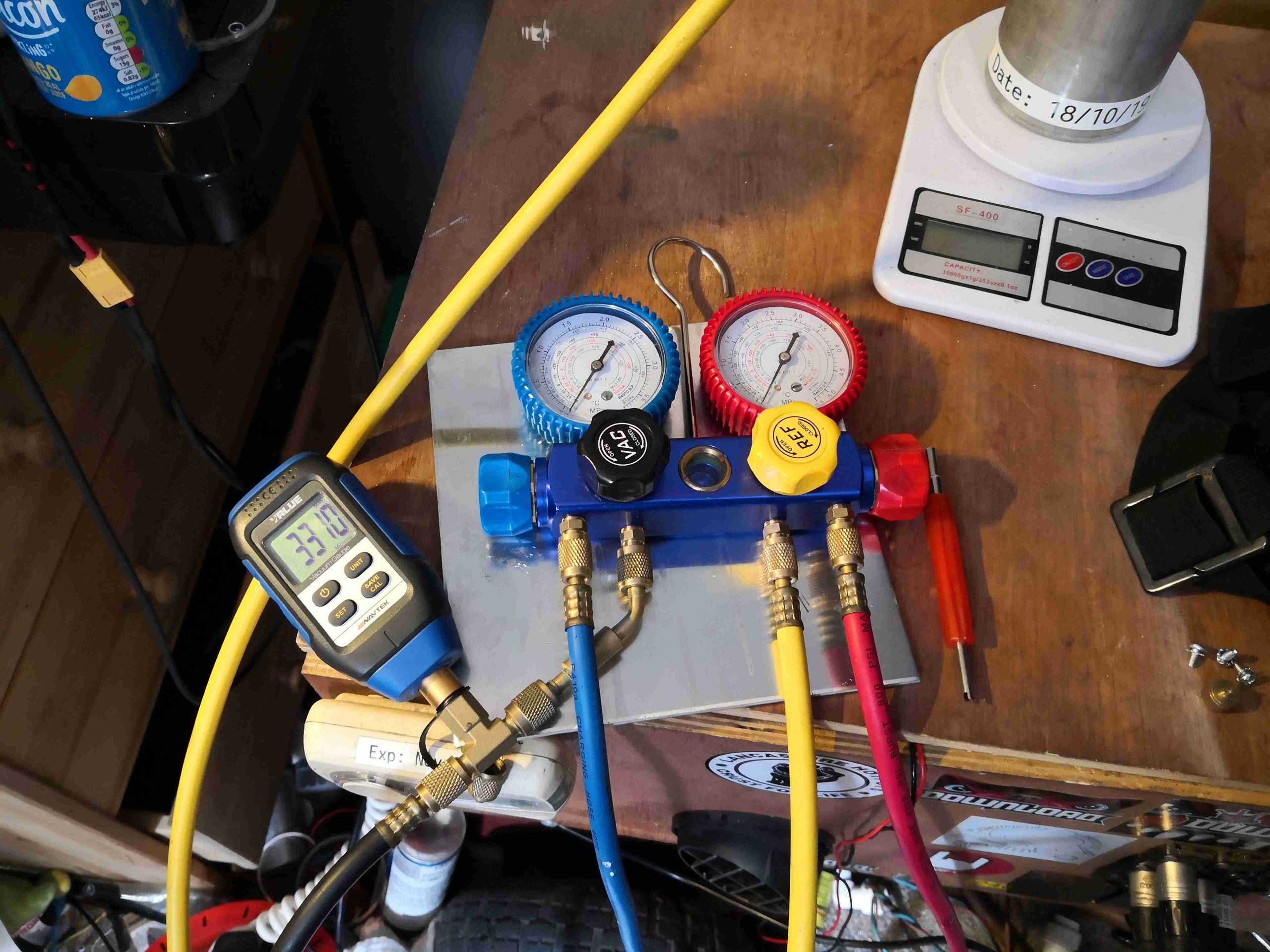
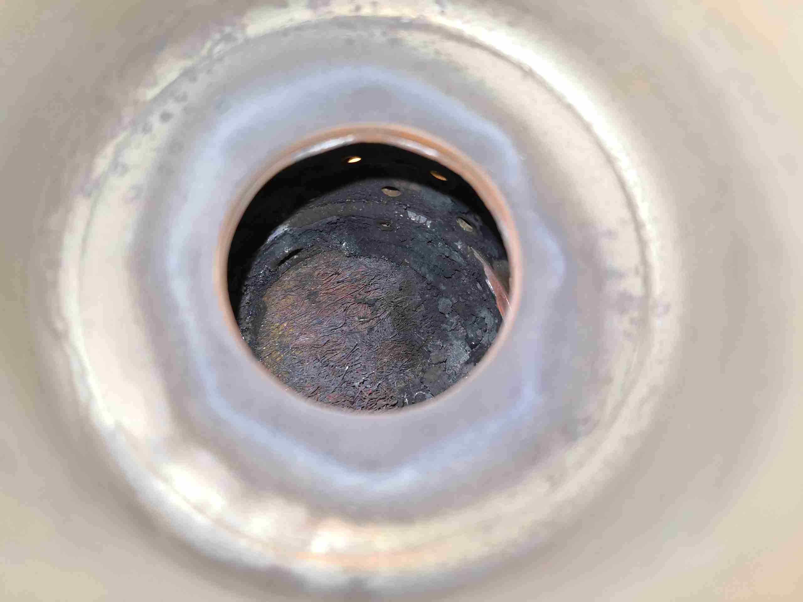
New System Charging
Once the new compressor was brazed into place, a full leak & pressure strength test is performed. I’m using isolation valves on the charging hoses here – they’re quite nifty. Backseat them all the way & the charging hose is isolated from the system. Front seat all the way & the hose valve is opened, and the Schrader valve core is depressed in the service port. They really cut losses when charging systems with Schraders!
Vacuum Stage
Next step is applying a vacuum to the system. I aimed for a final vacuum of 250 microns. This by far takes the longest amount of time in a refrigeration job. For reliability & longevity of the system, it’s imperative that all contaminants such as water vapour & air are removed from the circuit.
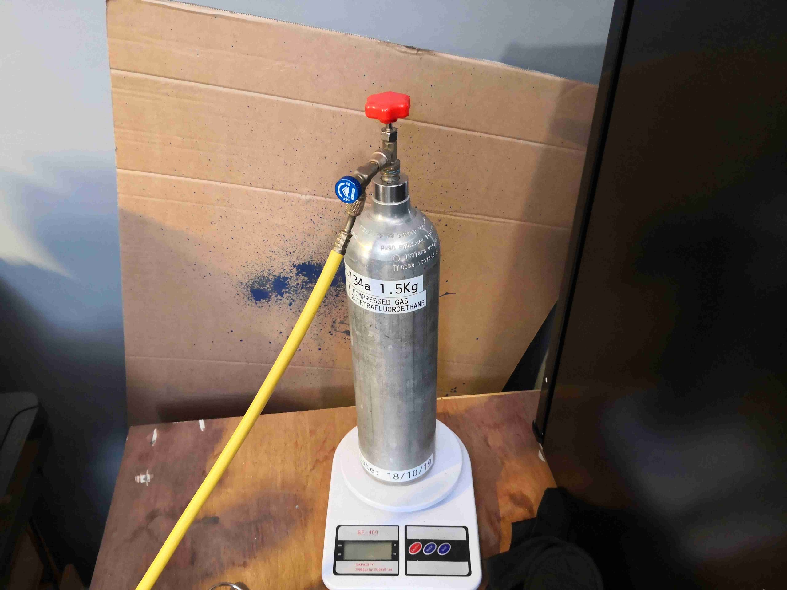
Refrigerant Bottle
The final step is a refrigerant charge. Since I’m not at all fond of flammable refrigerants in this use case (camping), I broke out the bottle of R-134a. This isn’t ideal, as the capillary tube will be sized for the original charge of R600a, but the effect on efficiency shouldn’t be too terrible. (There will be a drop in COP, but I haven’t yet measured the actual COP of the re-engineered system). Unfortunately, as this uses a plate evaporator with a built in capillary tube, there’s no way to resize this for another gas. The capillary tube is fed down the centre of the suction line in these systems, to increase efficiency of the cycle.
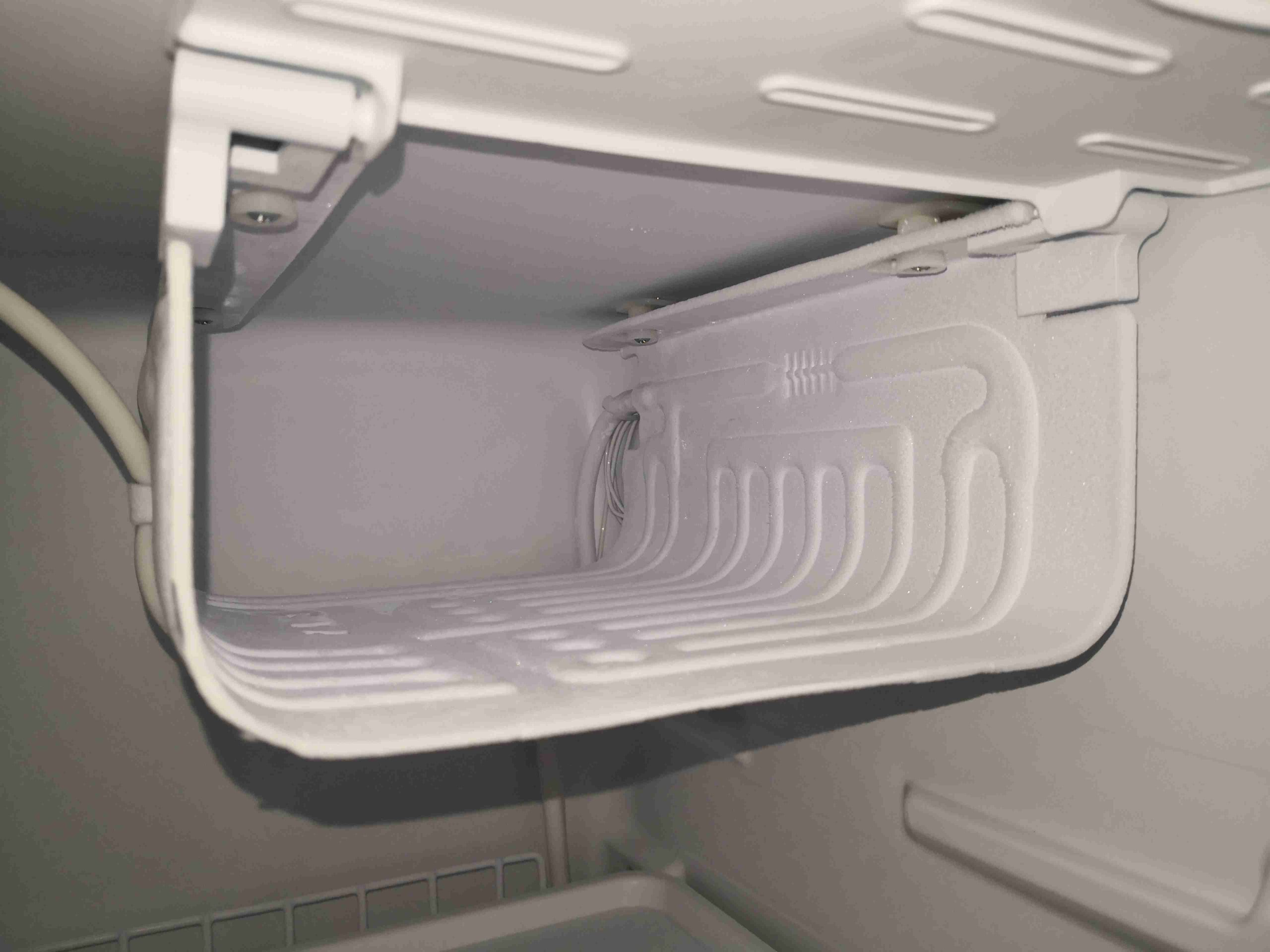
Evaporator
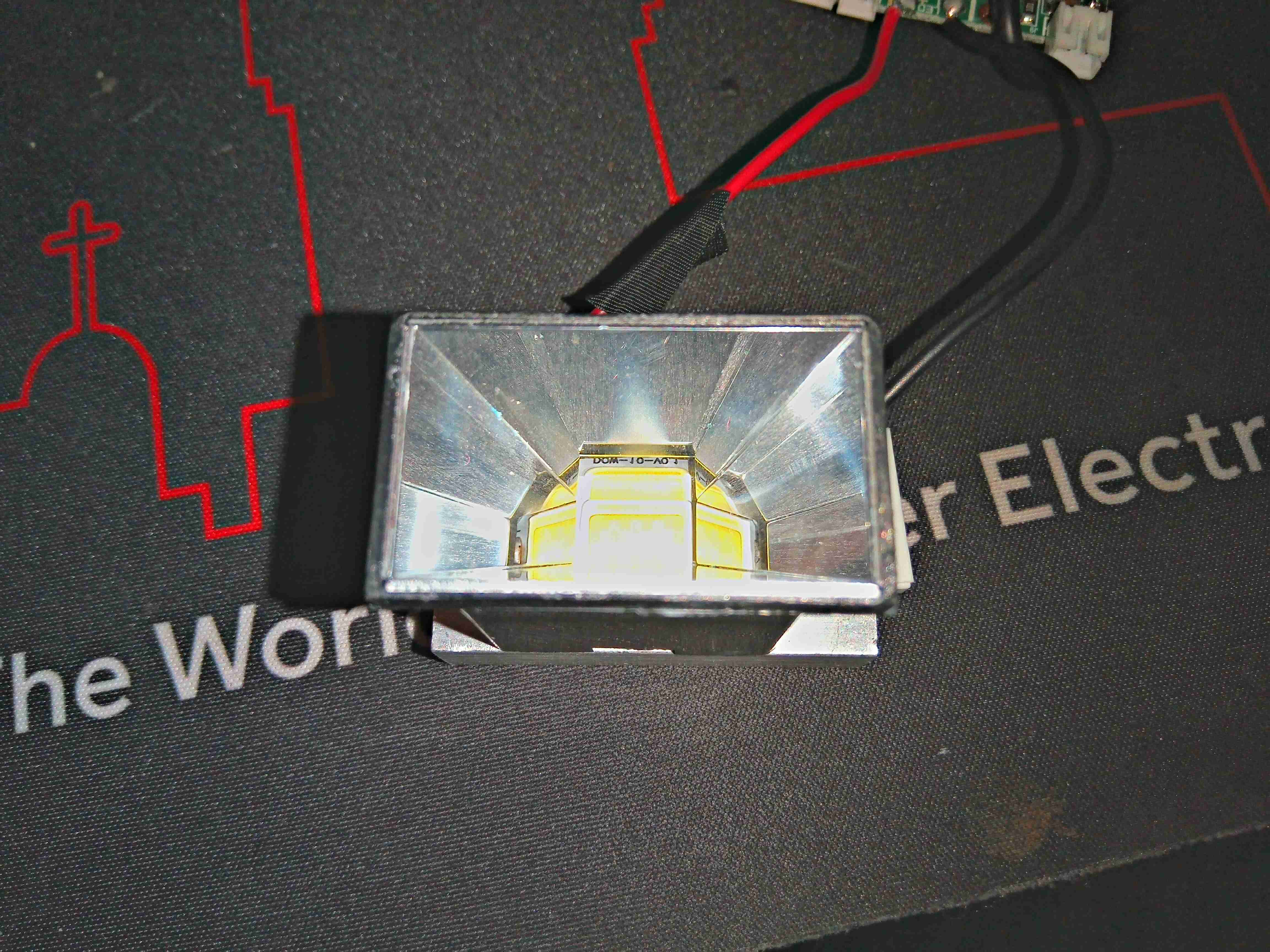
A few minutes after an initial charge of 45g R-134a, there’s frost on the plate evaporator! Since this is a gas change as well as the compressor, there’s no other way than to charge slowly, and wait for the system to stabilize at temperature. Then gas is added until there’s an even frost all over the evaporator surface. I would have measured the charge by suction line superheat, but I have no idea of the original system specifications.
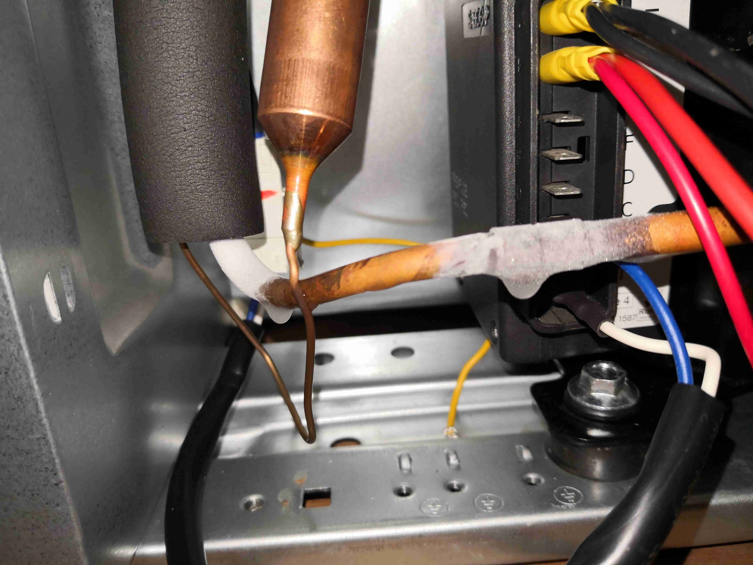
Suction Line Icing
In this case, when running the cabinet down to the minimum temperature possible, a slight overcharge became evident. Releasing a small amount of the refrigerant back into the charging bottle sorted this out.
I may yet make another modification to this unit, to remove the skin-condenser from the circuit. While cheap, and difficult to damage as they’re buried behind the outer case metal, they’re not very efficient. I have some small fan-cooled condenser coils that will probably end up in the back next to the compressor to improve efficiency. This will also take some of the heat load off the cabinet insulation, as there won’t be a coil of hot refrigerant next to it.
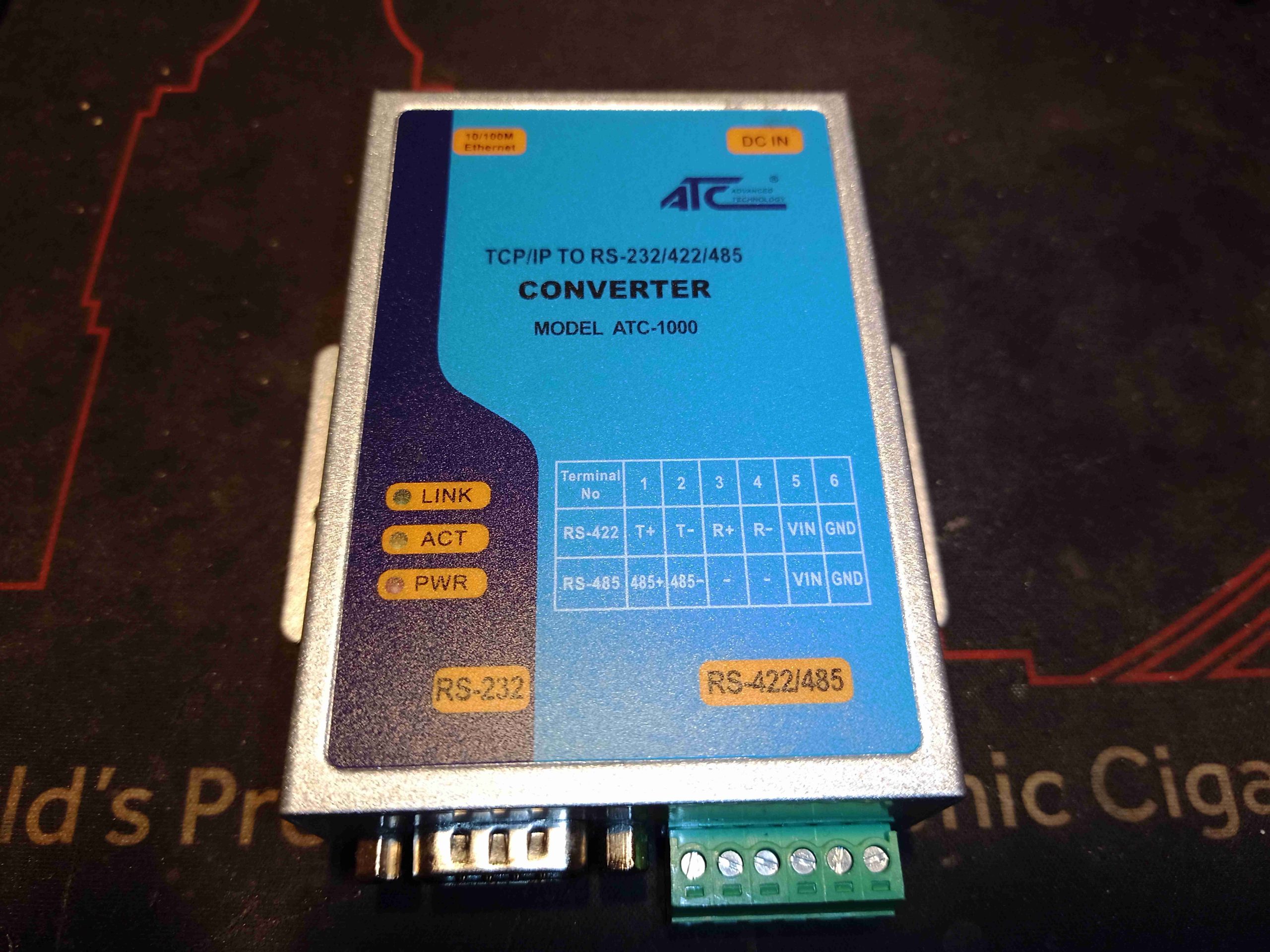
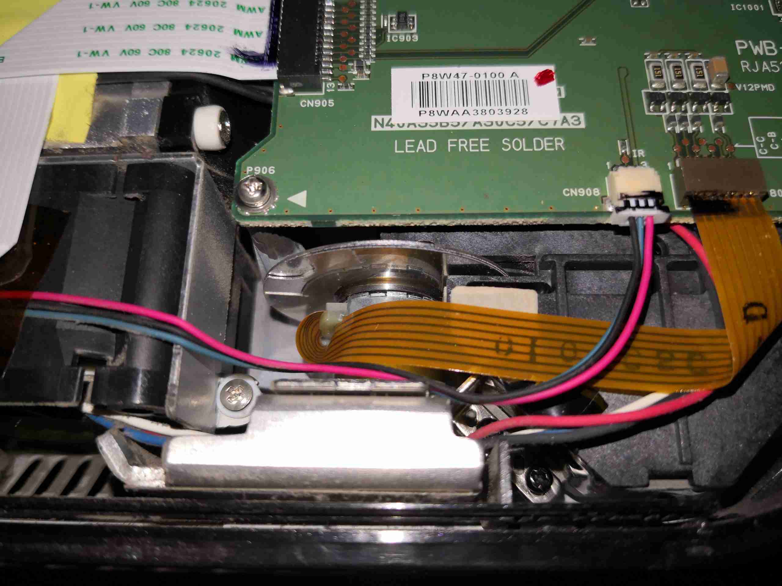
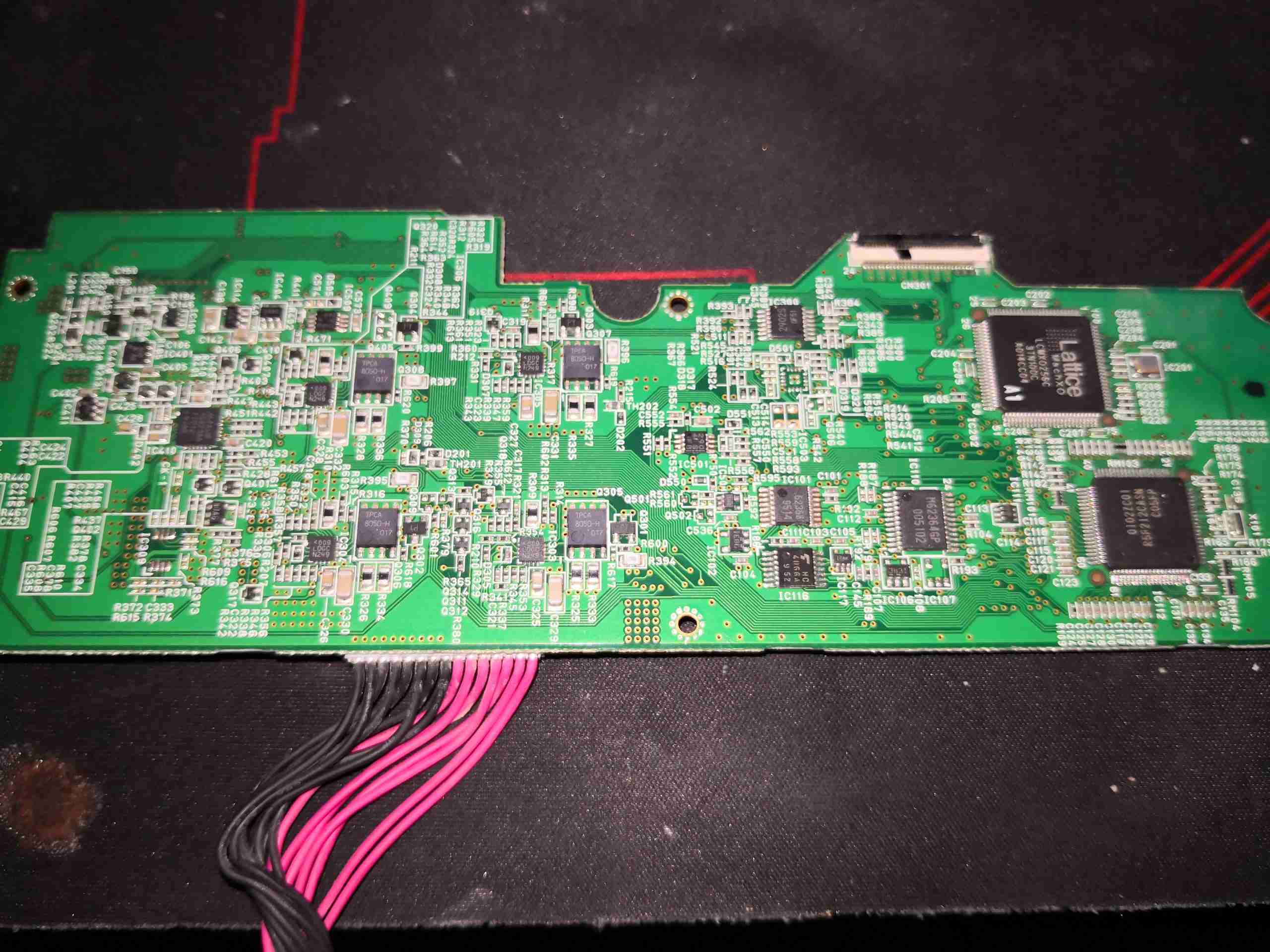
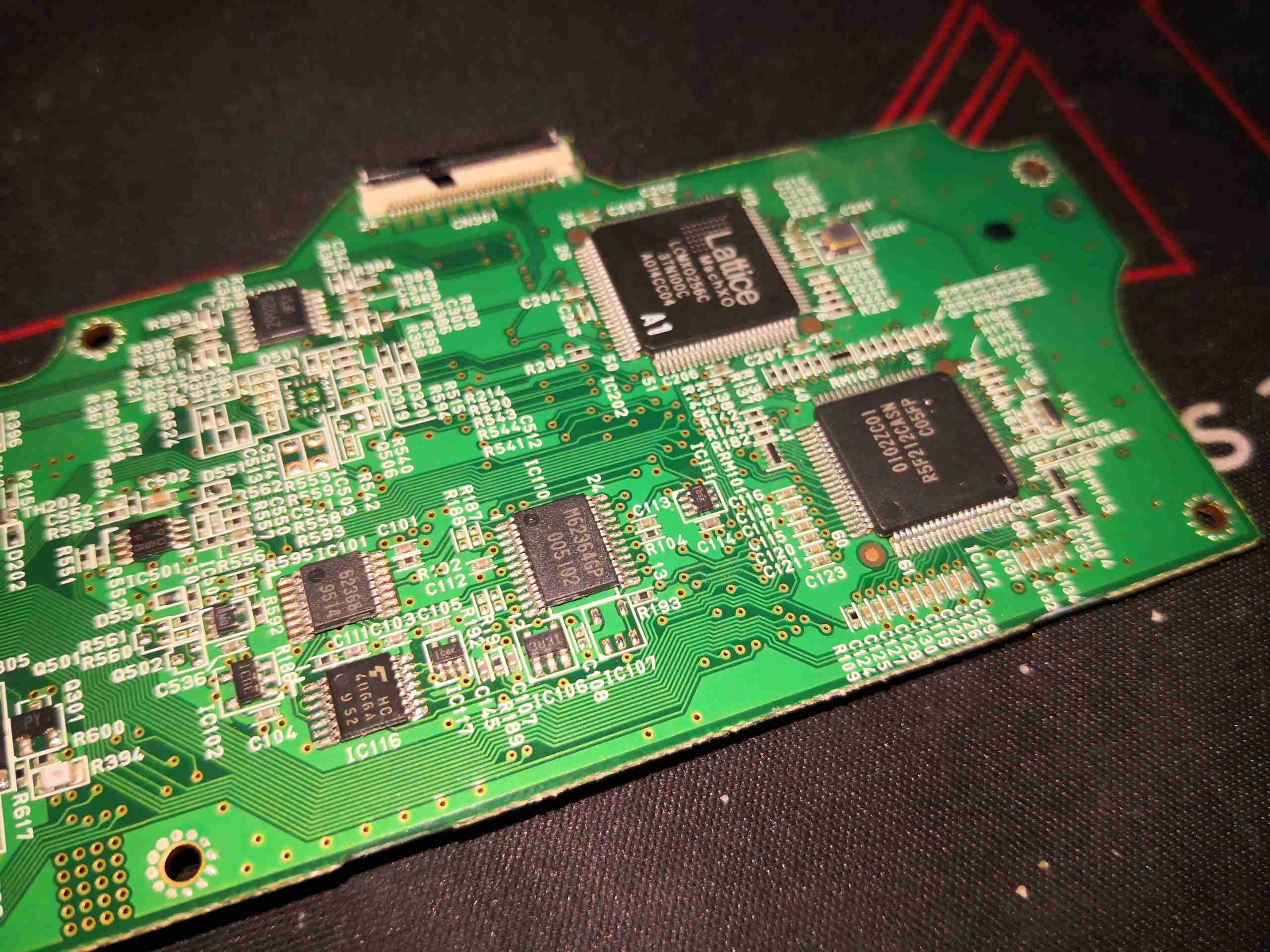
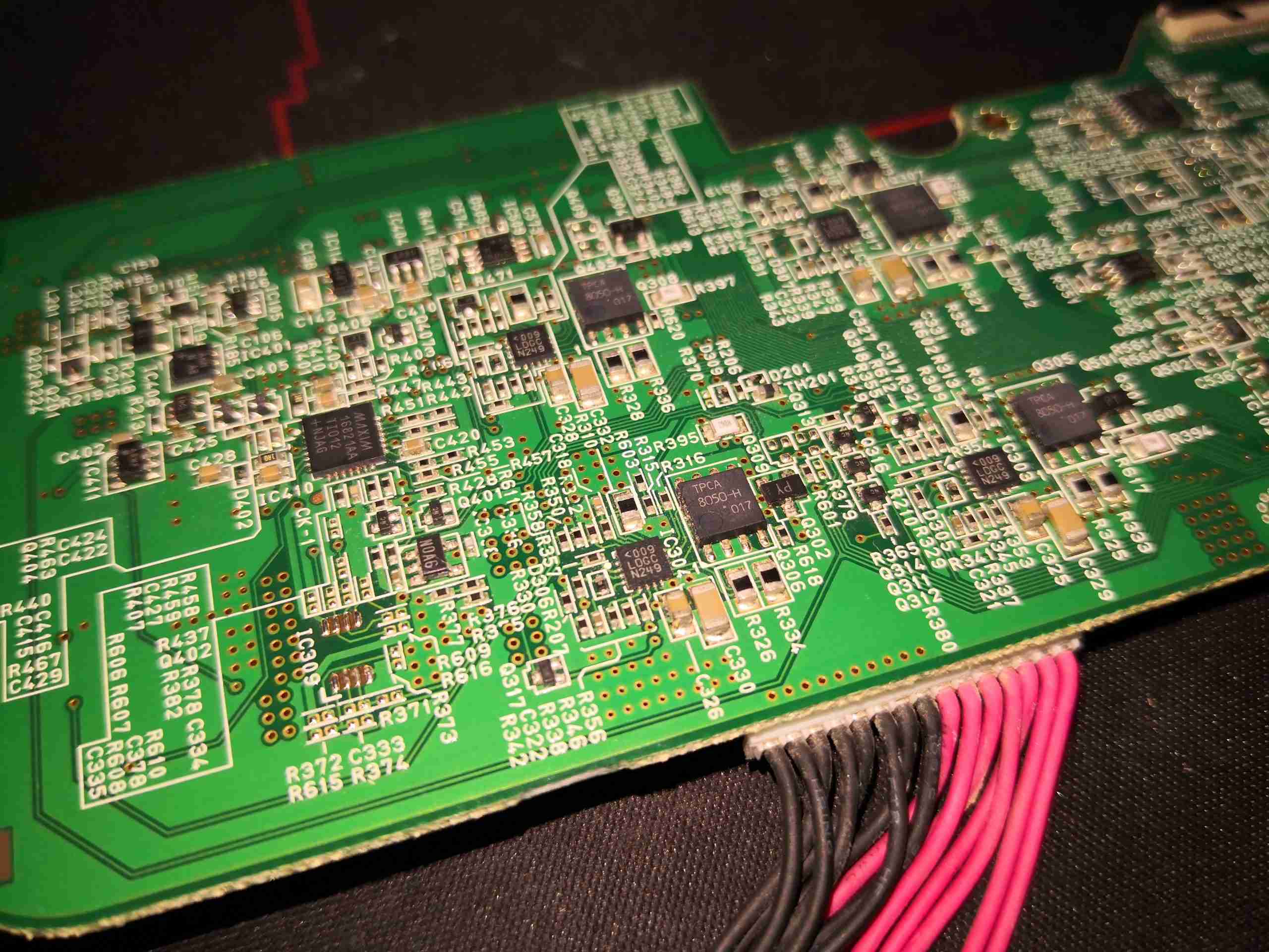
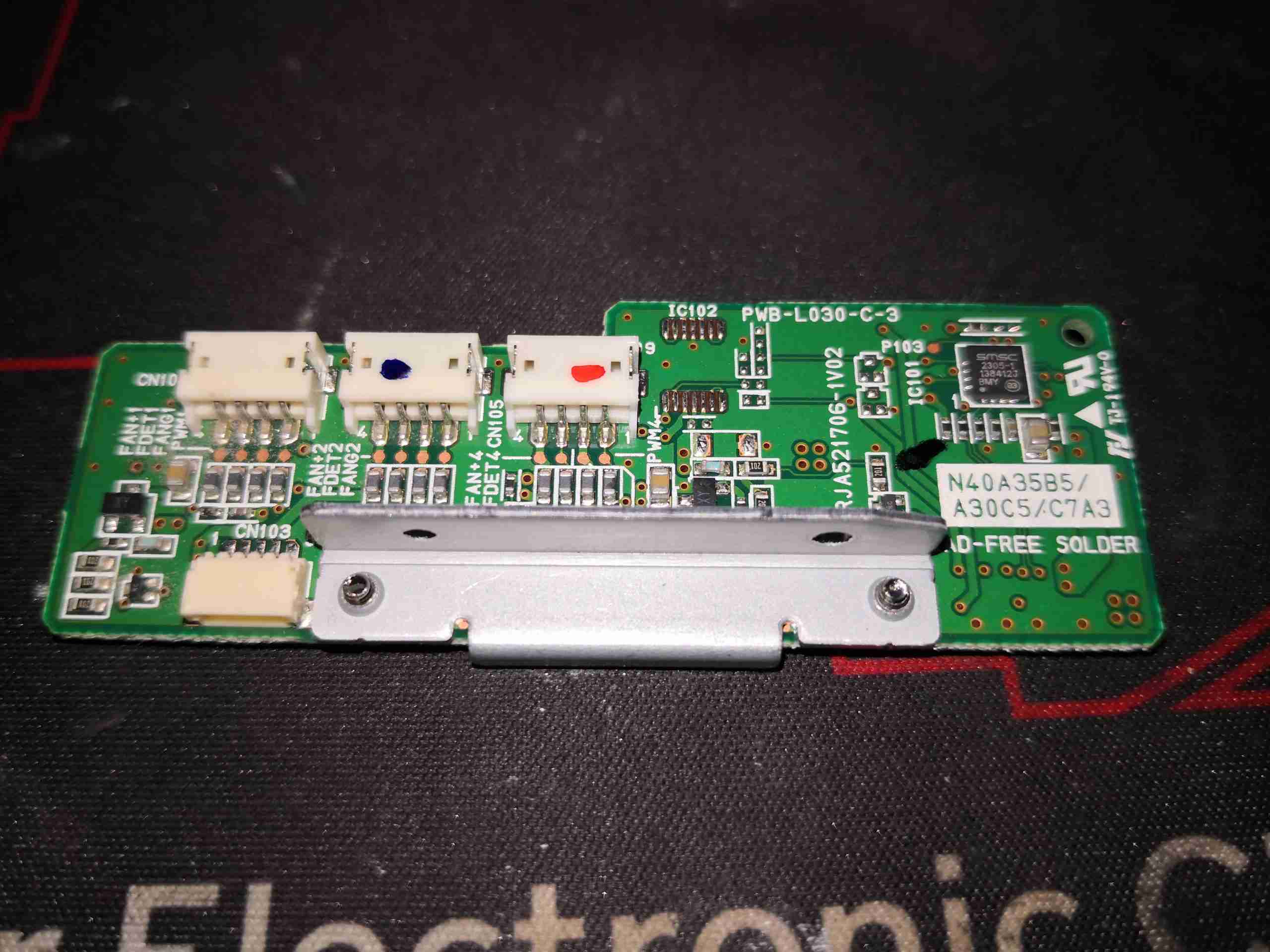
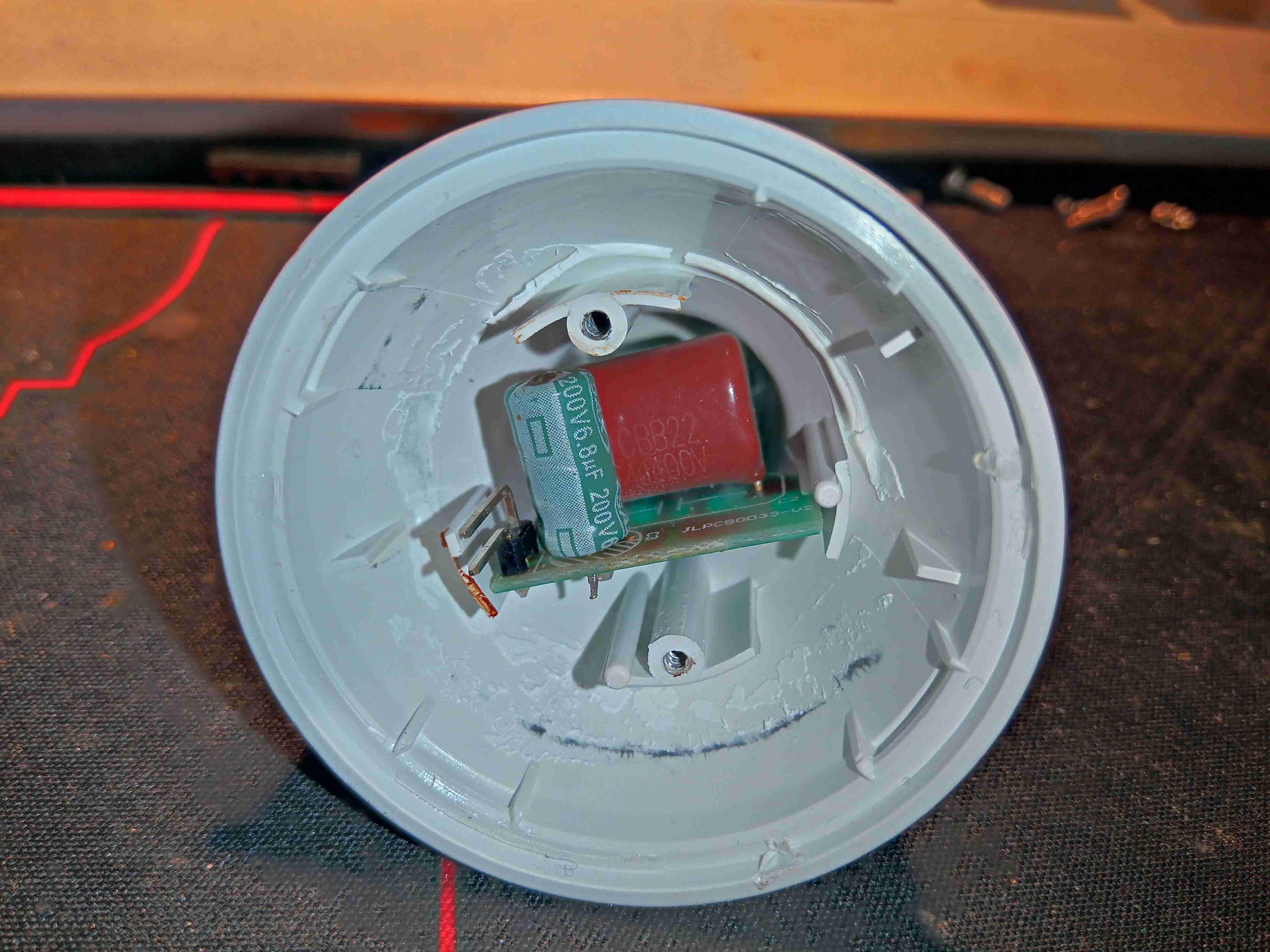
Just a quick teardown this month! This is an industrial RS-232/RS-485 to Ethernet serial converter.Not much to say about the outside of the unit, there’s the DB-9 connector for the 232 interface, and Phoenix connector blocks for the 422/485 interface. The main power input, and the Ethernet jack are on the other side.
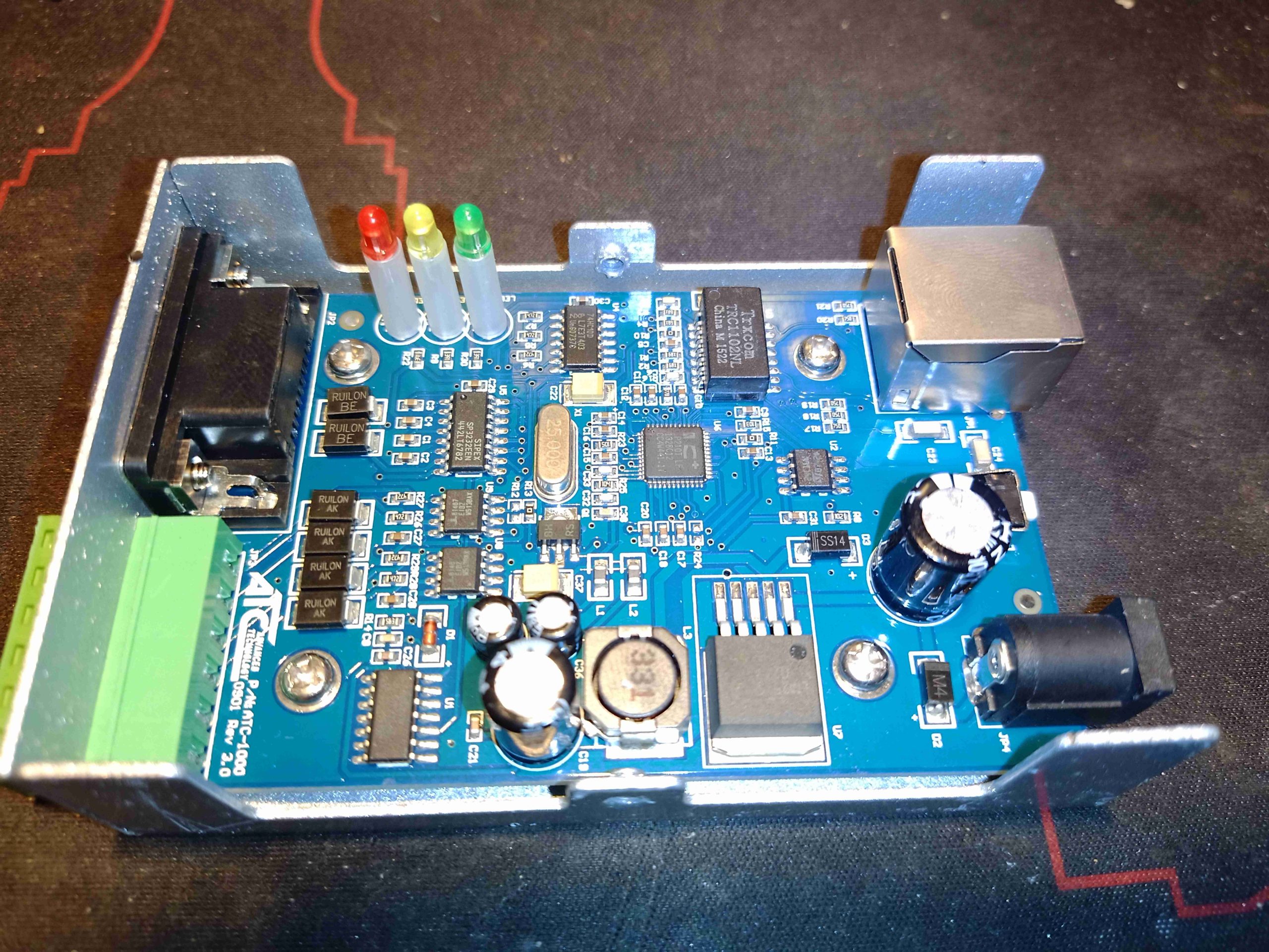
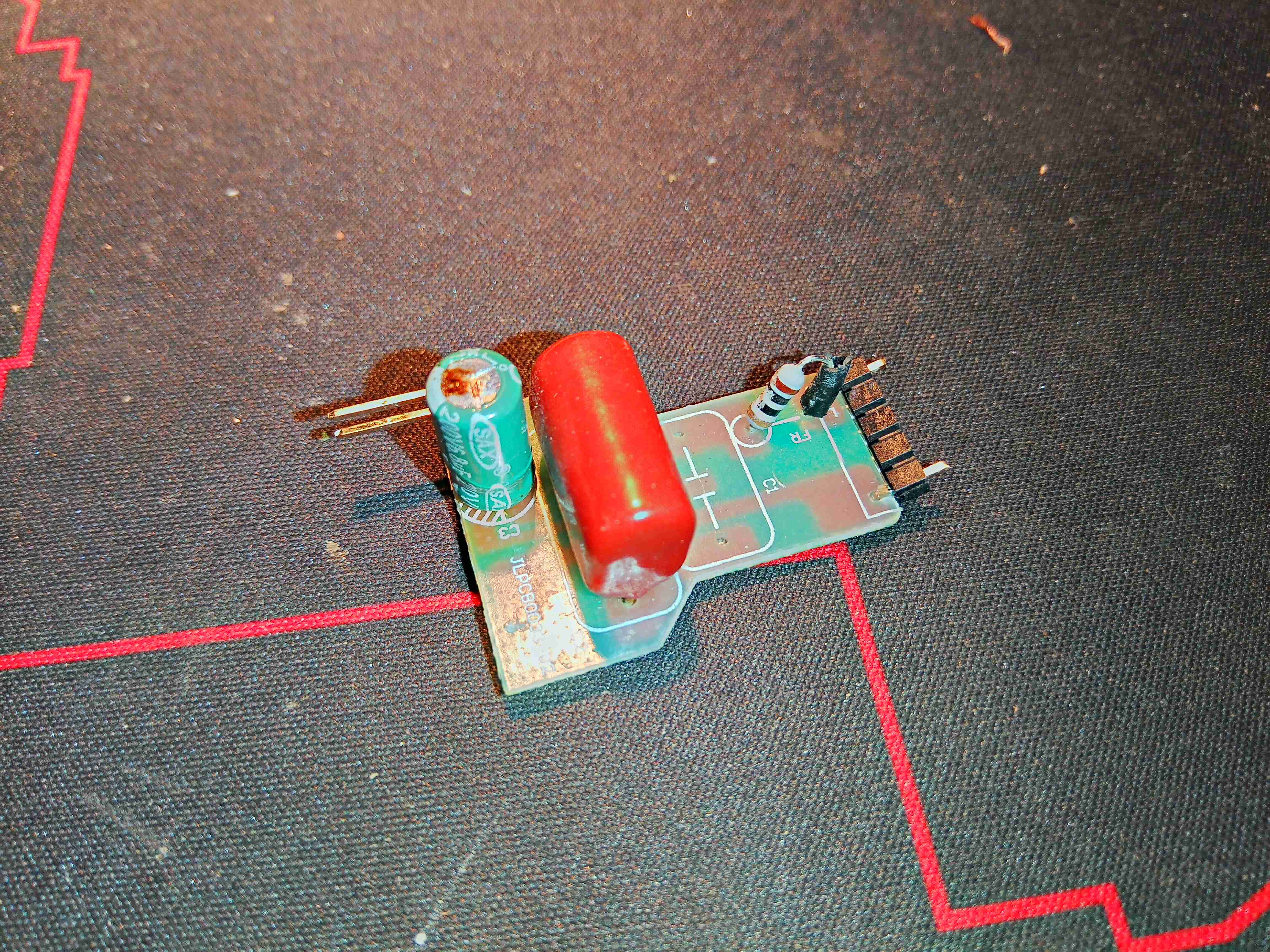
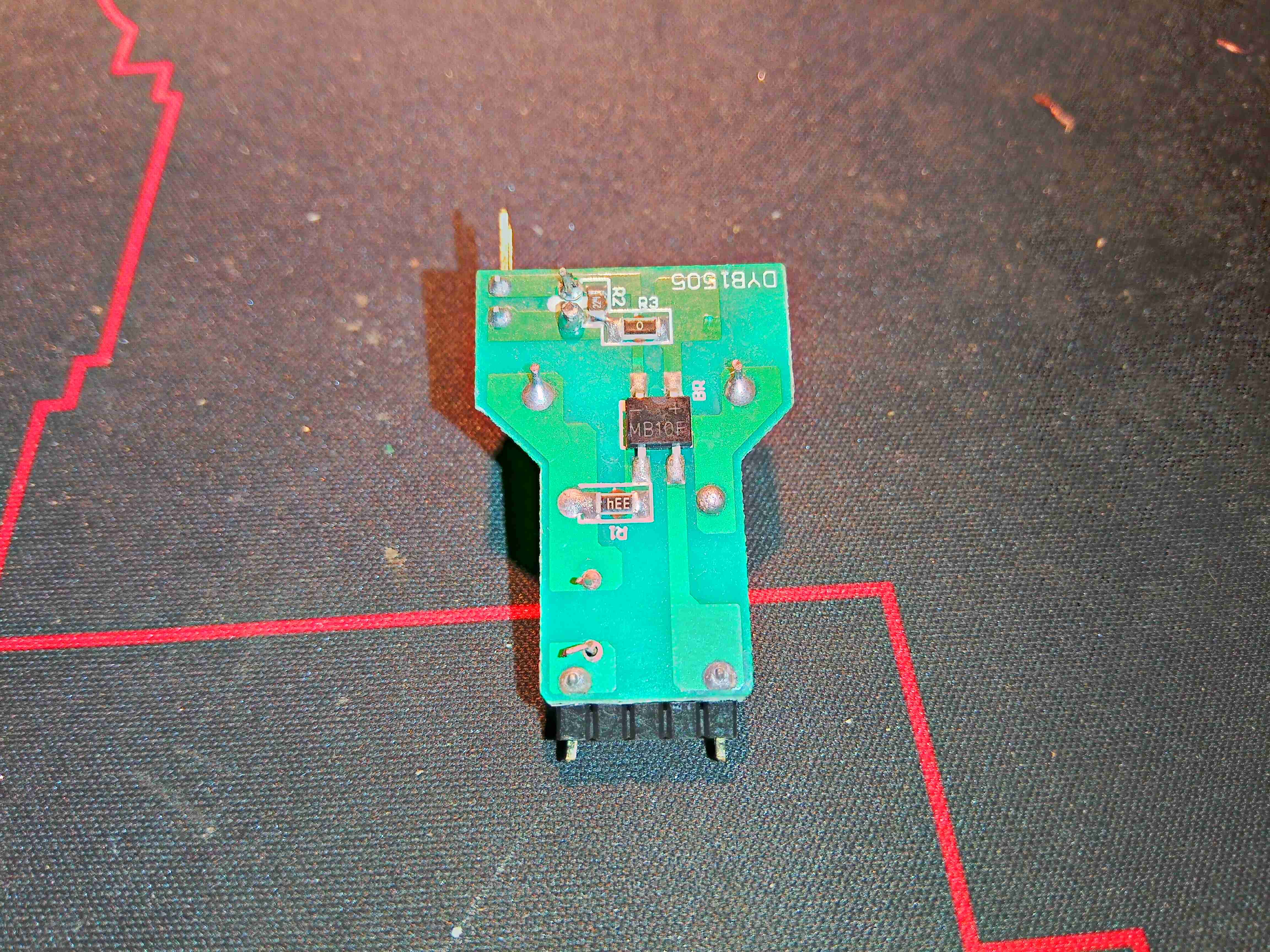
PCB
Under the hood, there’s a pretty densely populated board. The brains of the operation is a IP210T Serial to Ethernet SoC with A/D Converter. This is an 8051 based core, wuth 10/100 MAC. No flash memory here either, only 64KB of OTP EPROM. On the left there’s a few bus transceivers to interface the serial ports, along with some glue logic. At the top we have the Ethernet magnetics, configuration EEPROM for the SoC & a trio of indicator LEDs.
Power supplies are dealt with via an LM2576-3.3 DC-DC buck converter, providing the main 3.3v rail for the logic.
On the front of the head is the filter carousel. In this case it’s only fitted with a 2.5mm Aluminium filter. These are used to filter out the low-energy X-Rays from the beam, reducing the overall dose to the patient of radiation that does not contribute to the resulting image, as these lower energy rays are totally absorbed.
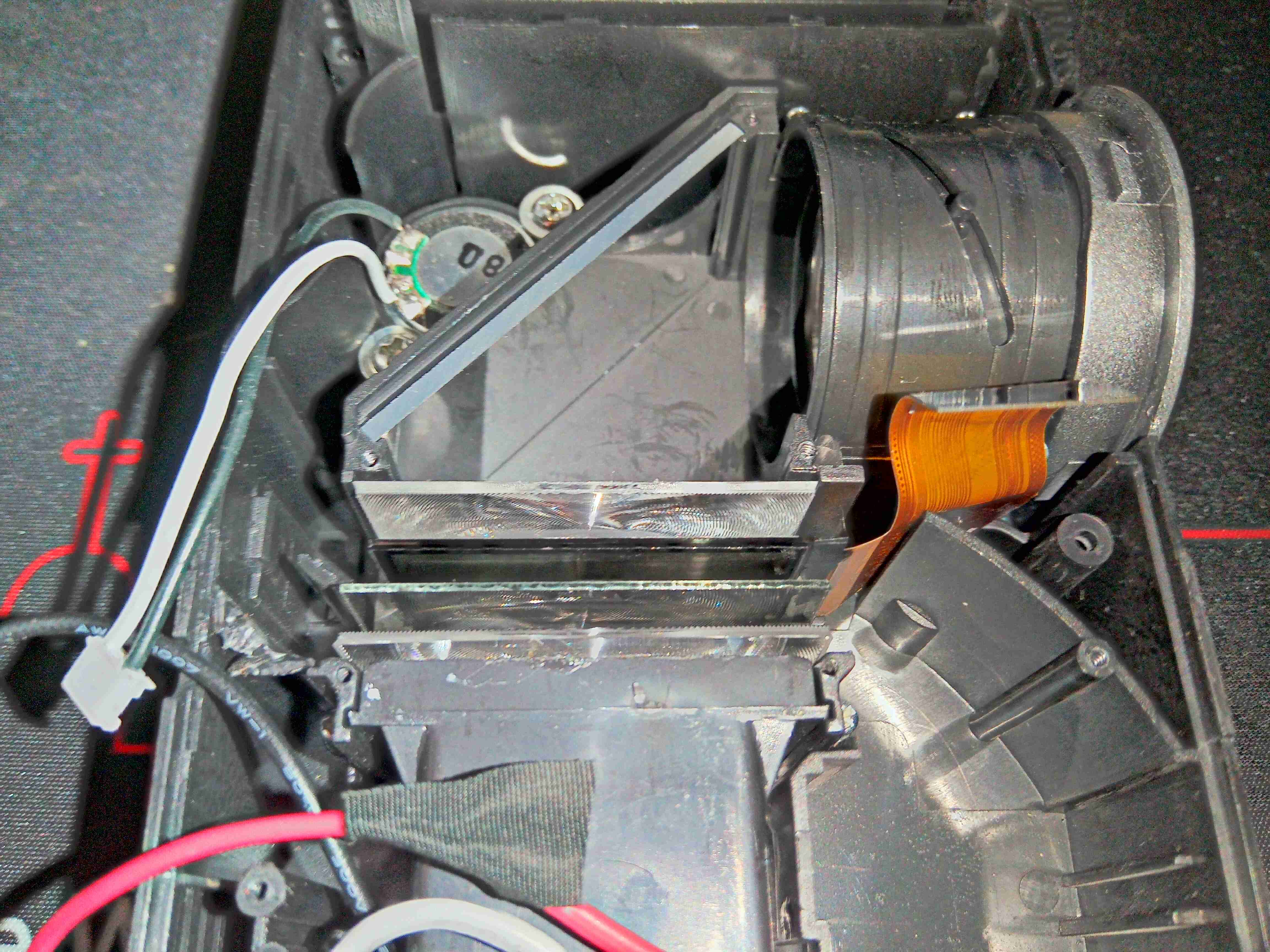
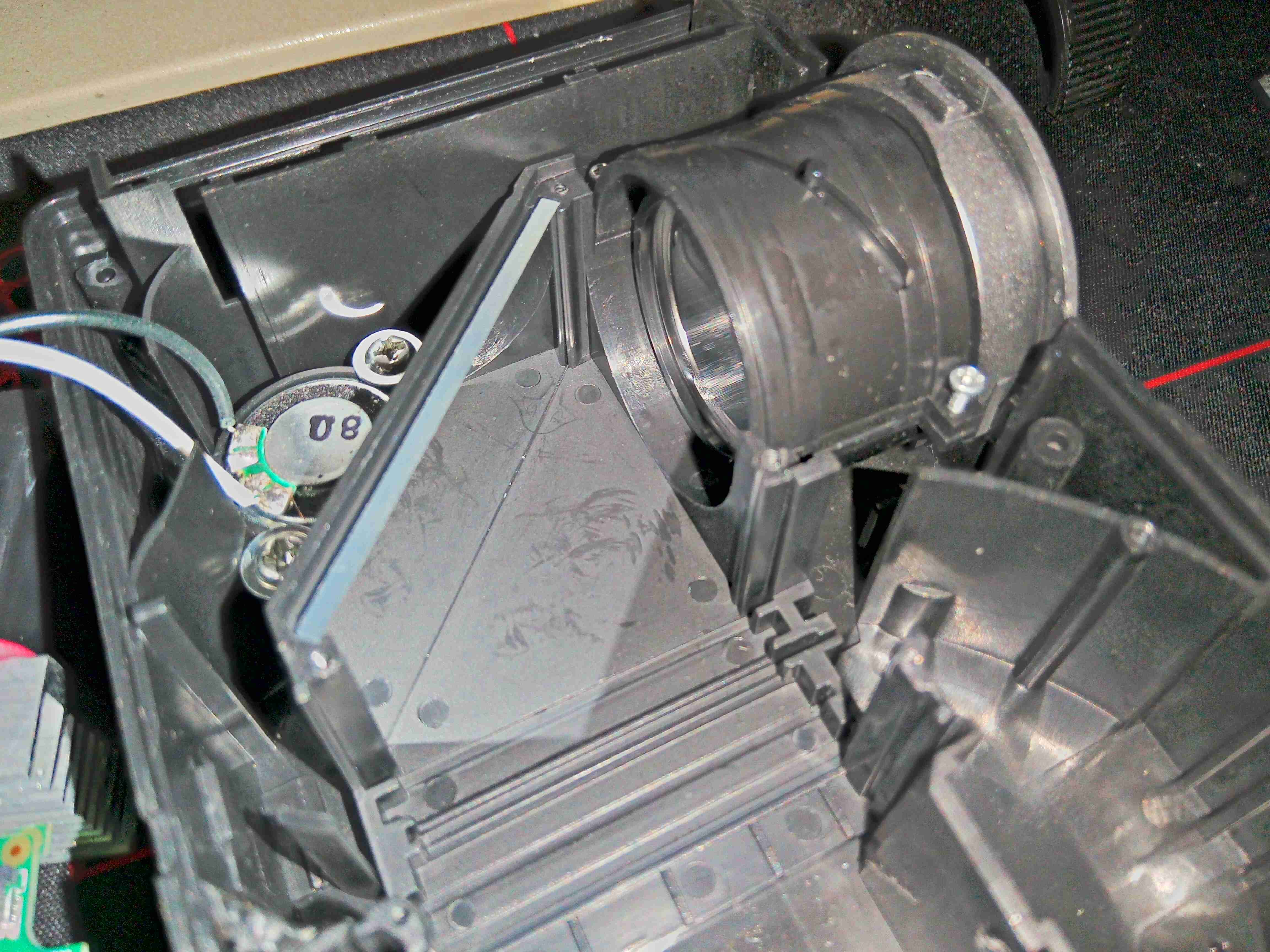
Top Cover Removed
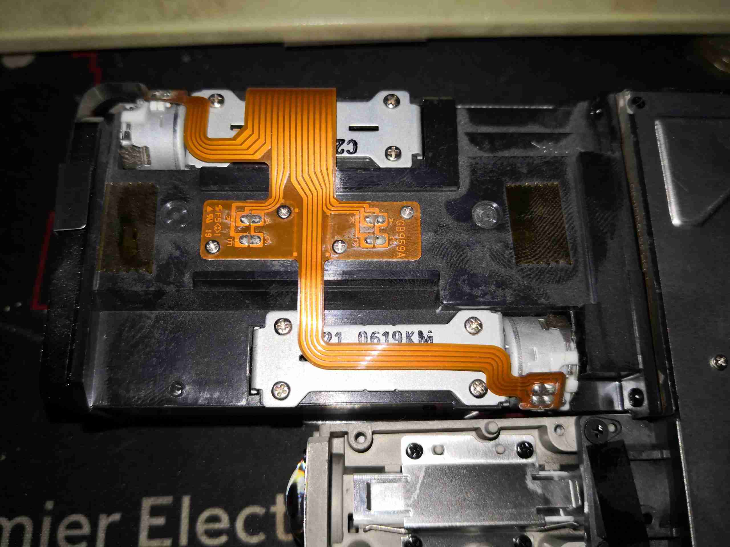
Removing a lot of cap screws later & the O-Ring sealed cover comes off the head. Unsurprisingly, this is full of dielectric mineral oil for insulation & cooling. There’s not much to see yet, as most of the components are hidden inside the plastic housings. The expansion bellows is at the top left, and the main HV transformer bottom left.
Wiring Feedthrough
All the wiring to the head is fed through this plastic plug in the side, which is O-Ring sealed into the casting to prevent oil leaking out.
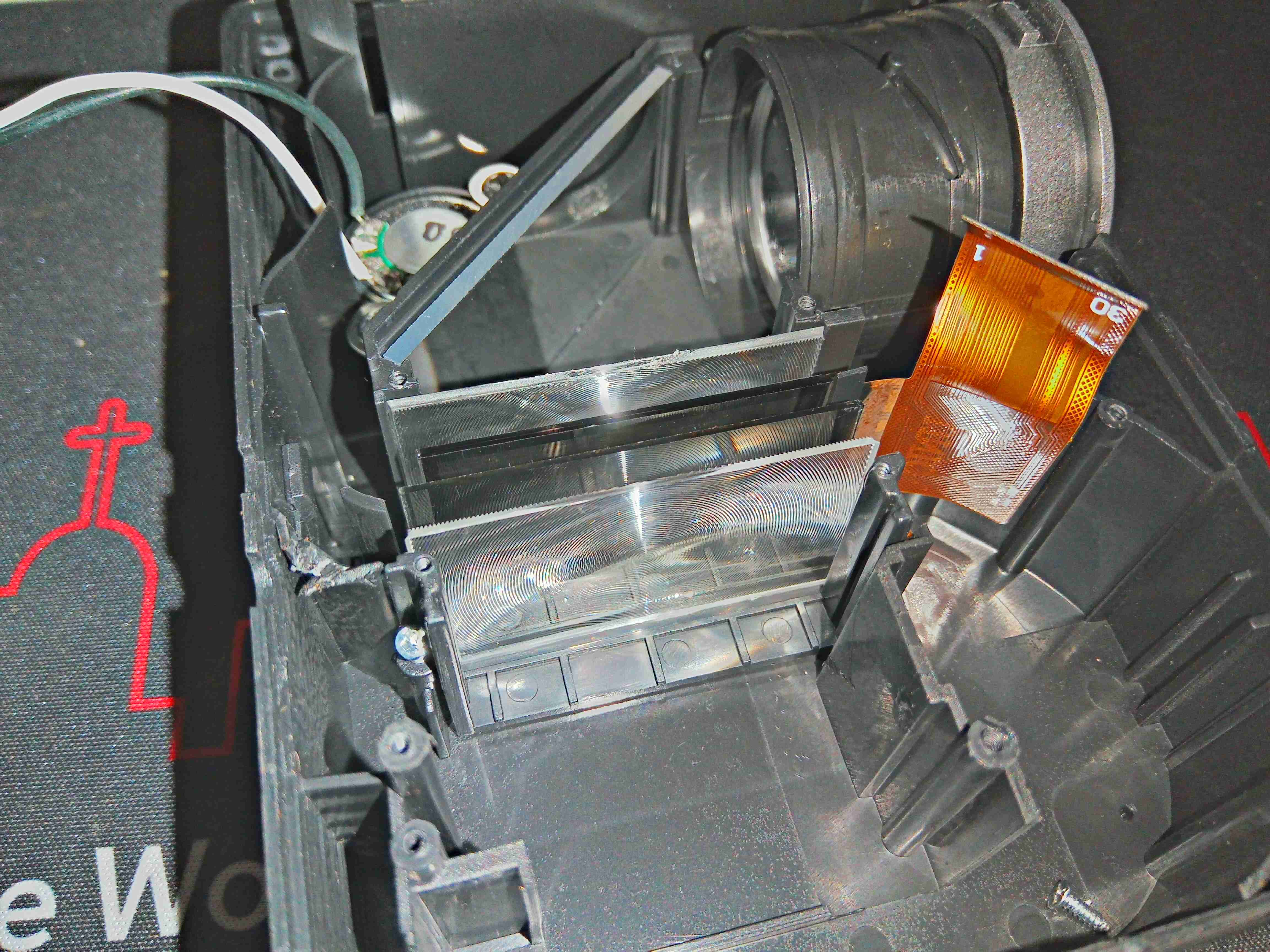
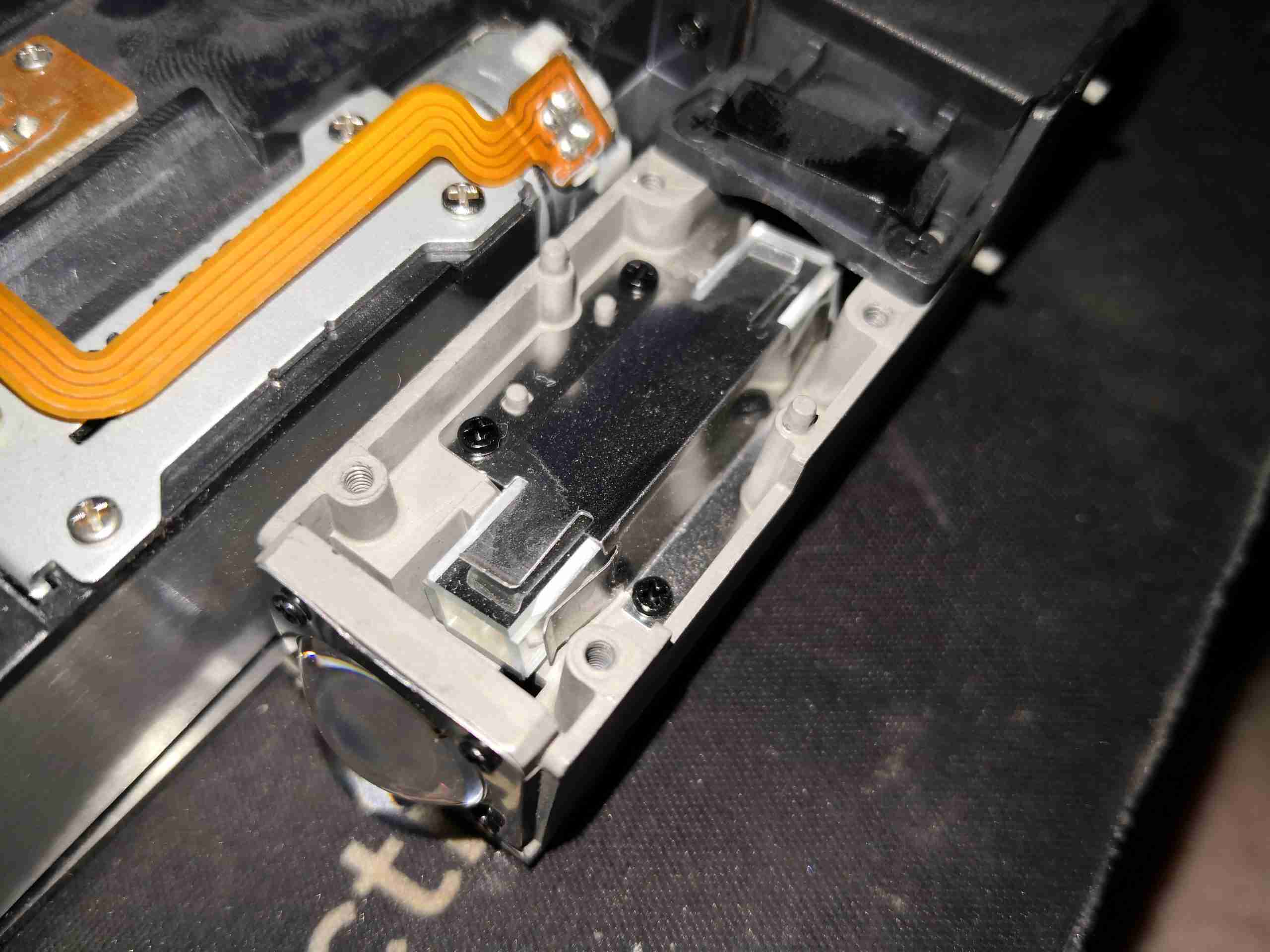
Tube Assembly
A clean bottle, syringe & some oily mess later, I manage to get the core out of the housing. This unit had about 3L of oil! The main HV transformer is hanging off the lower left corner of the plastic frame here, with the rest of the PSU behind it. The X-Ray tube is hiding within a metal shield in the tube to the right. There are no primary drive components present in the head – all of that is in the rest of the X-Ray machine.
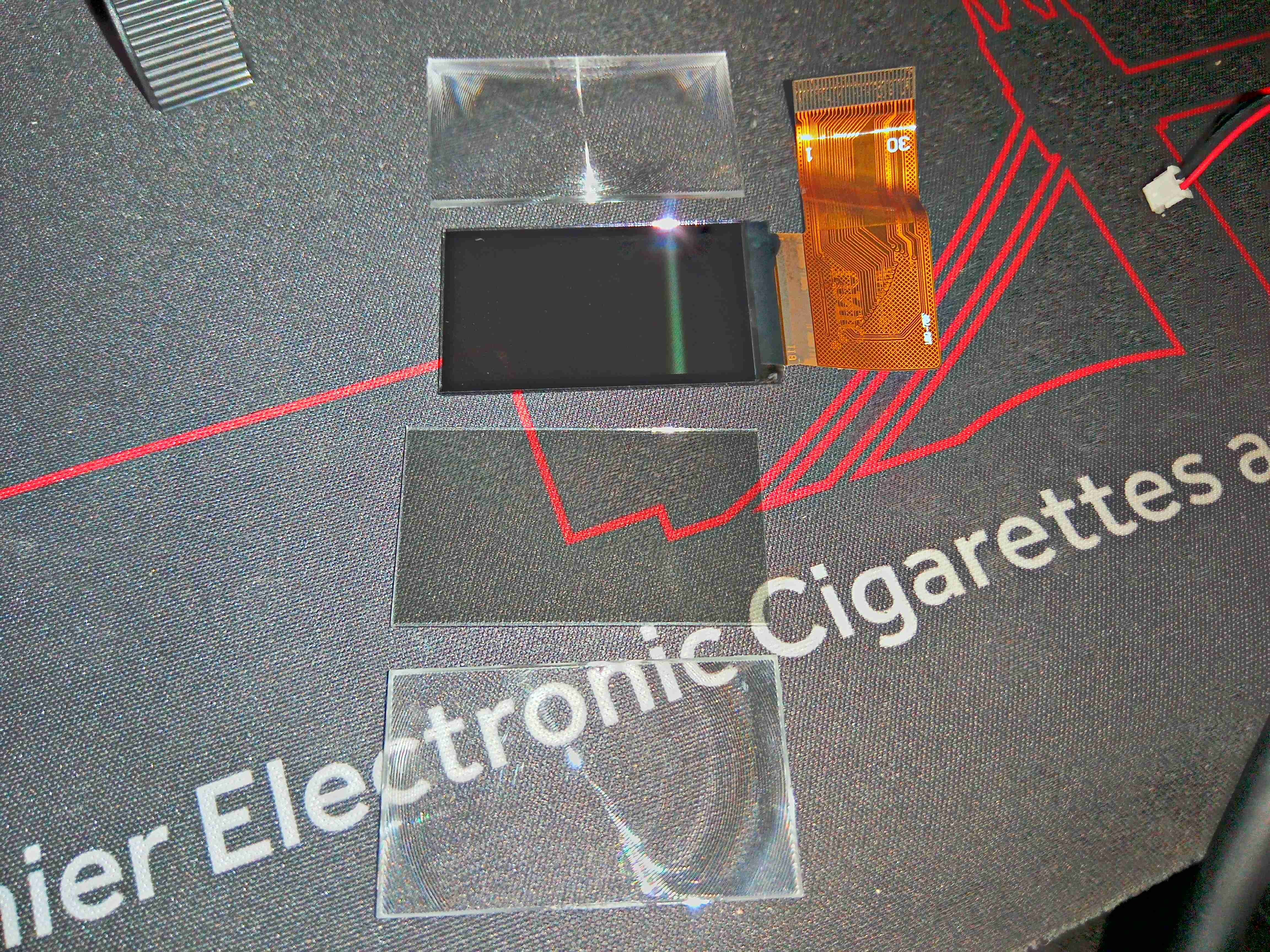
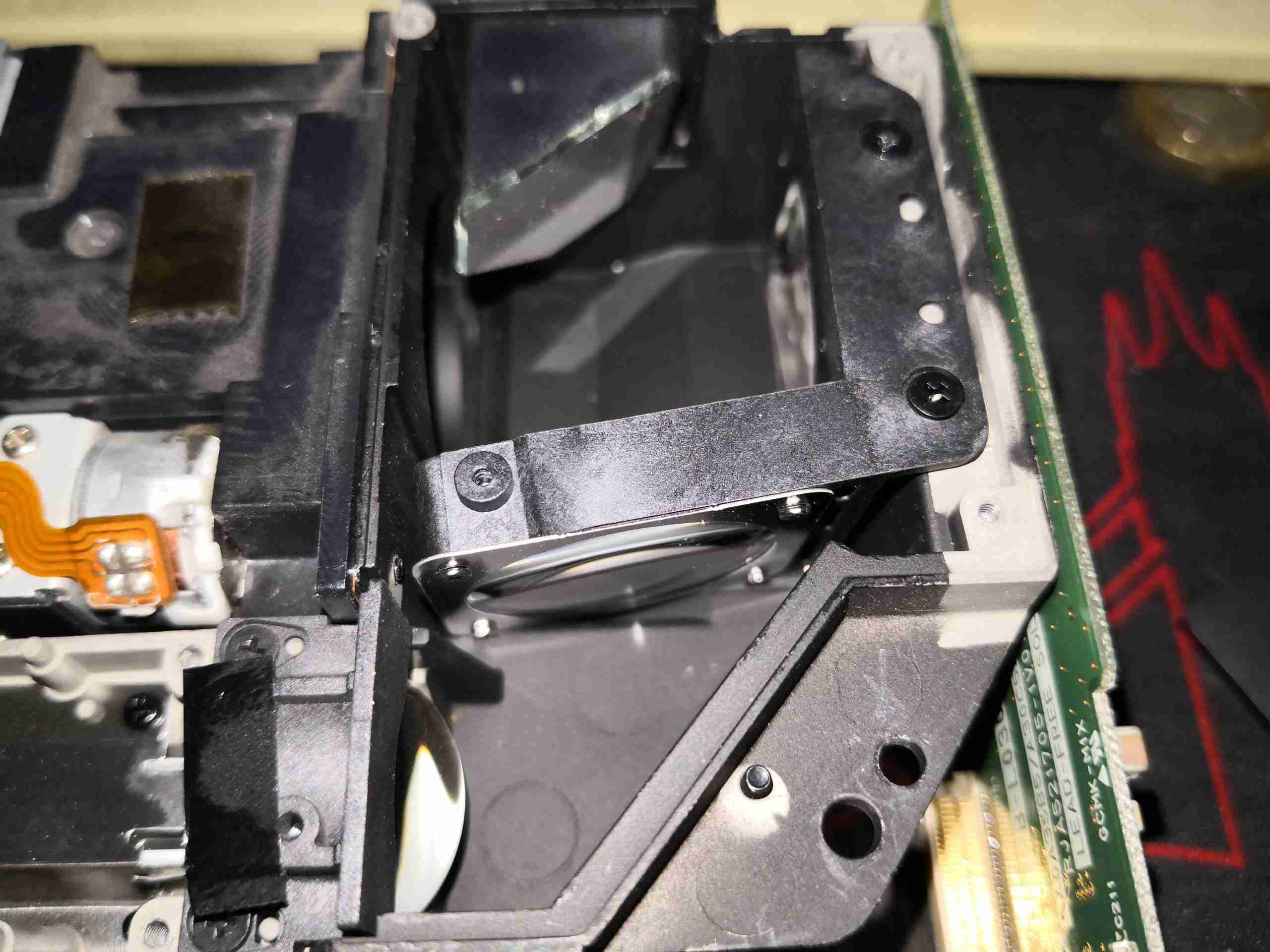
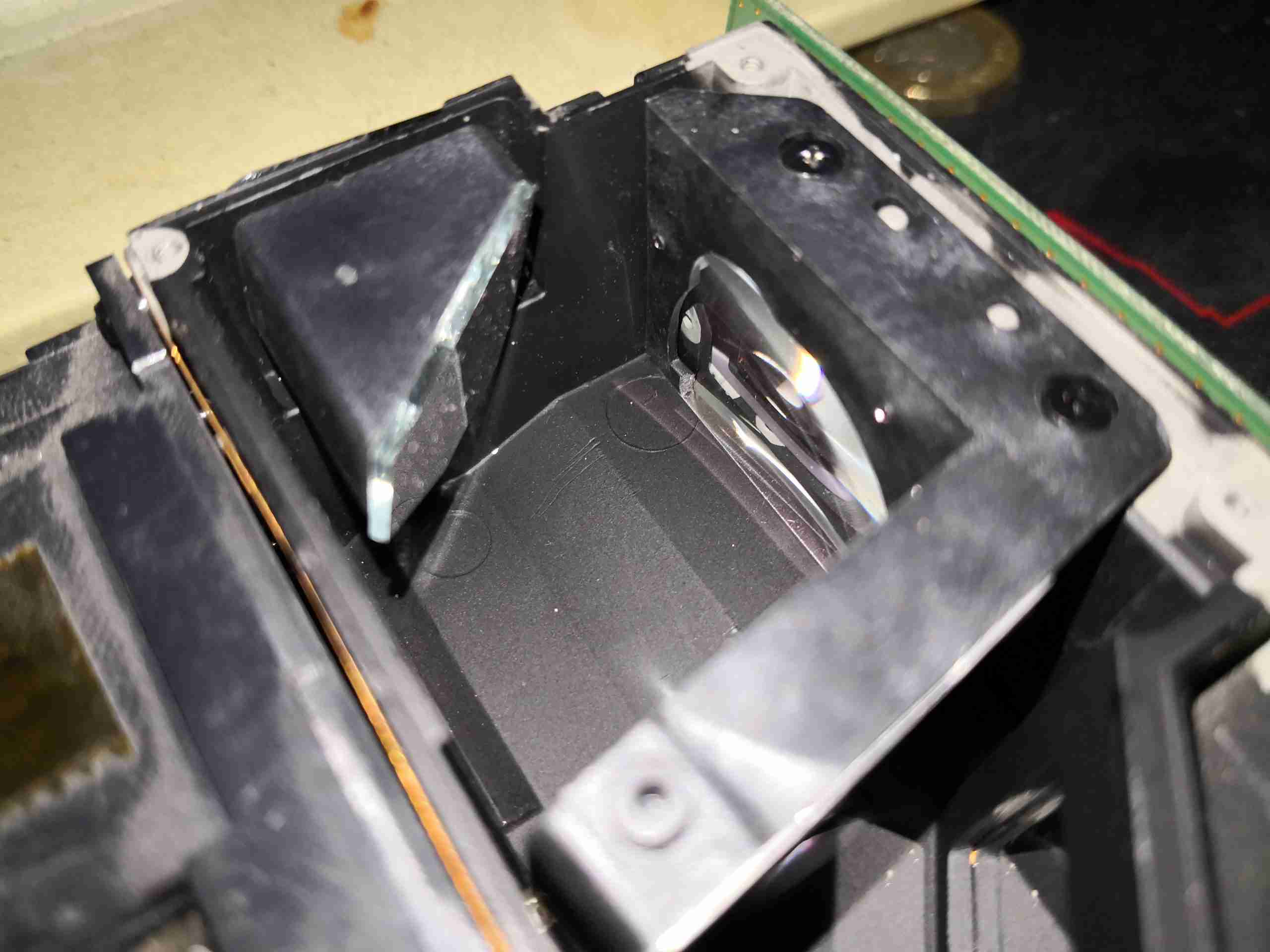
X-Ray Tube Sleeve
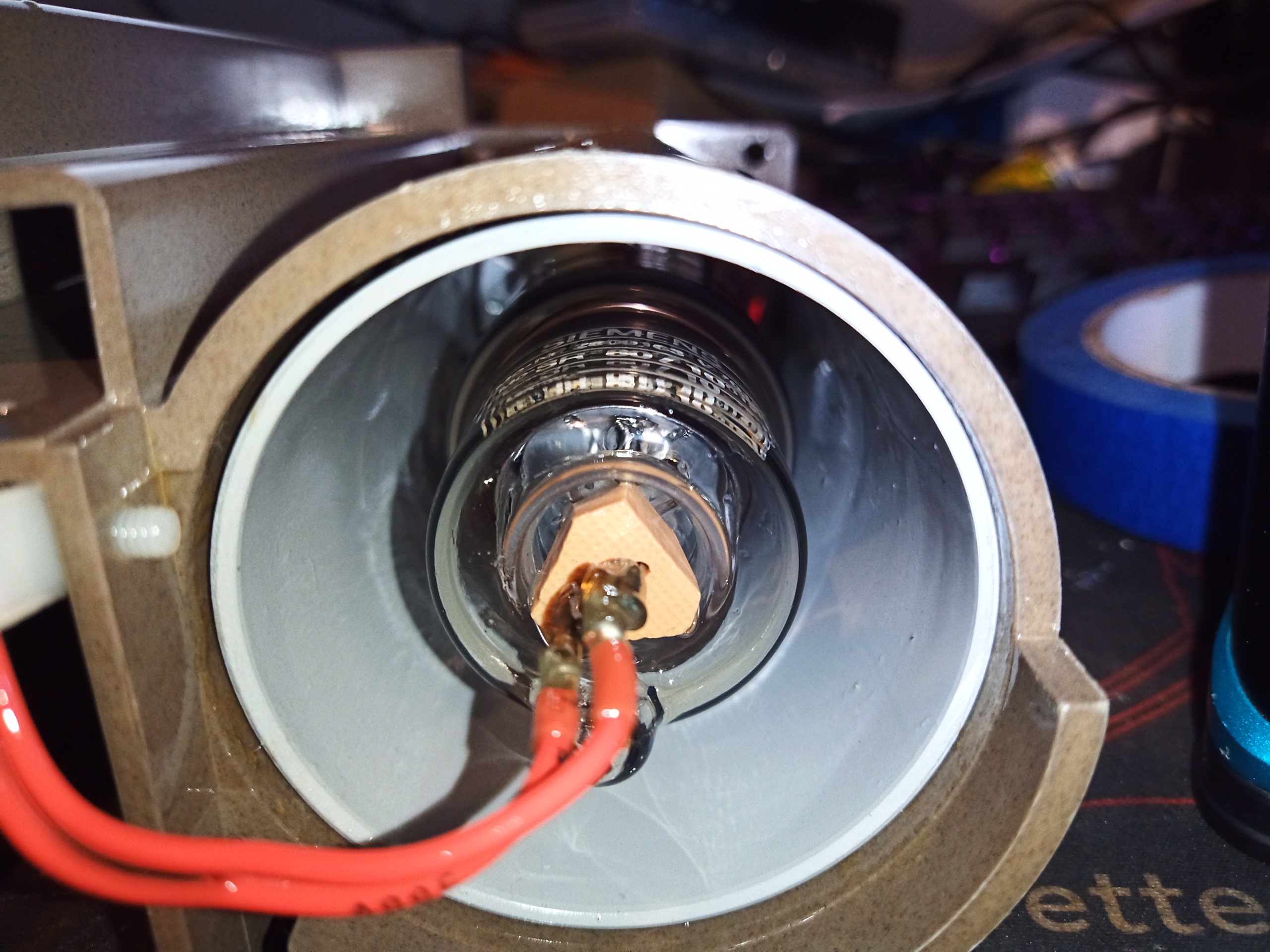
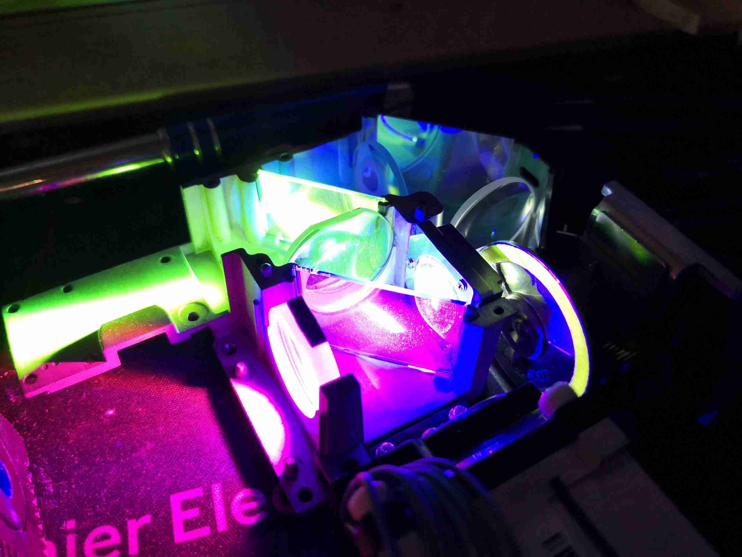
A look down filament end of the X-Ray tube. There’s a shield around this, likely to help stop stray X-Rays, and to provide some electric field strength distribution, as this is connected to centre of the HV PSU’s voltage multiplier, biasing it at around +40kV.
Voltage Multiplier
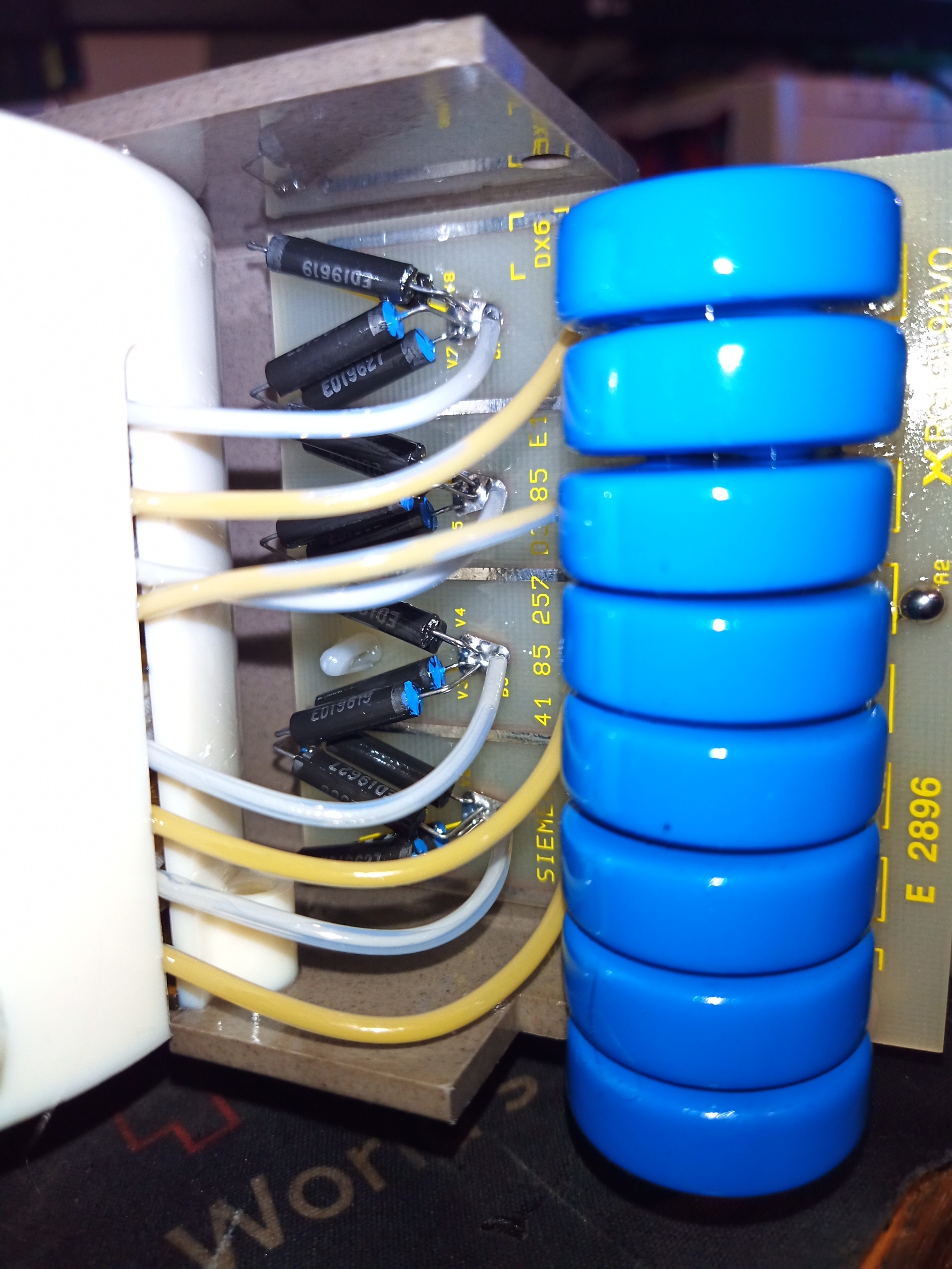
Behind the transformer lies the rest of the PSU – a 4-stage voltage multiplier. There are 4 separate secondary windings on the transformer, each feeding a voltage doubler. This is to keep the high-voltage stress on the transformer windings to a minimum, as the windings themselves only see 10kV per section, instead of the full output voltage of 80kV. This is increased to 20kV per section by the full-wave doubler, and as these are all in series the output end has the full 80kV.
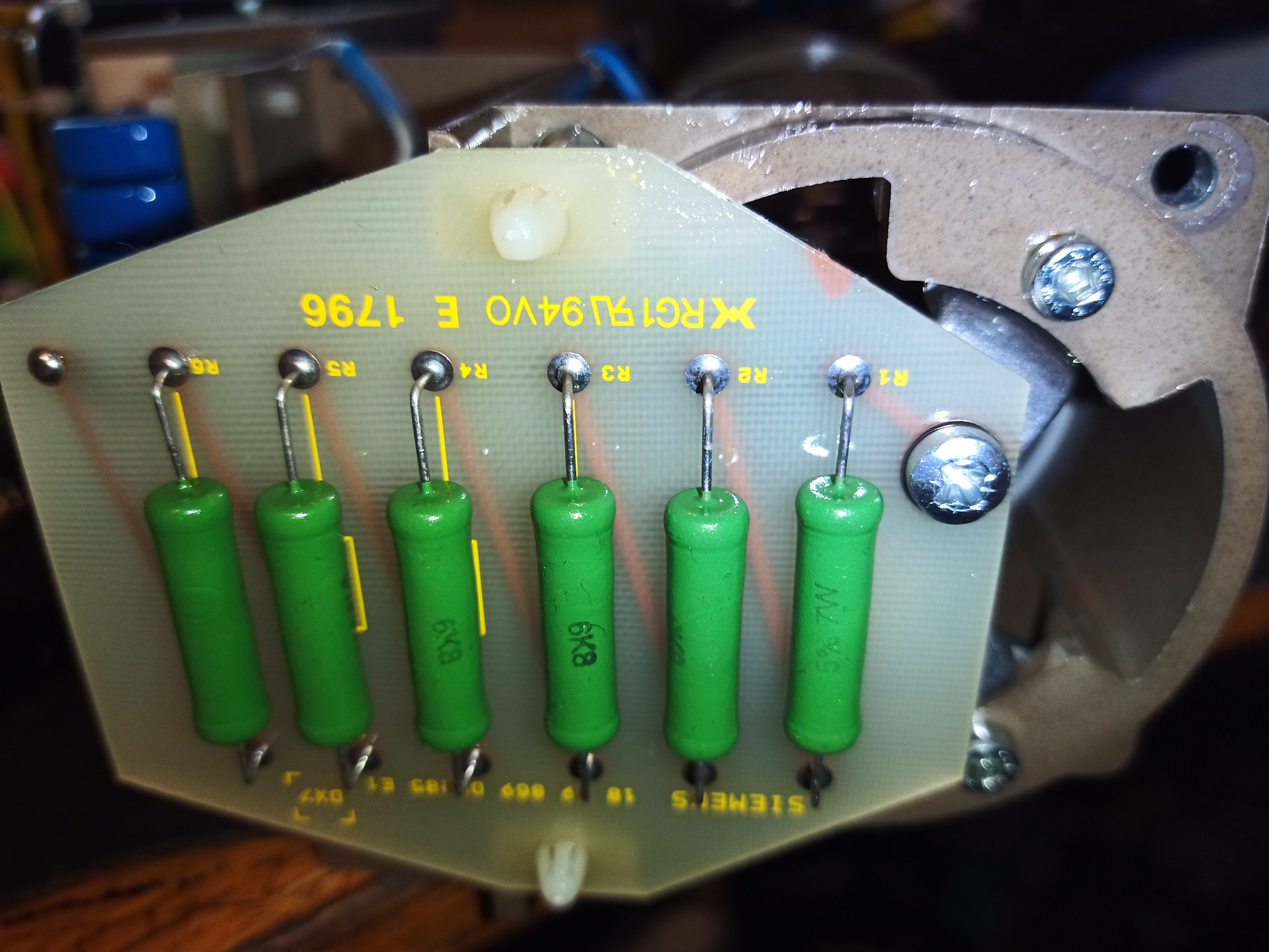
Ballast Resistor PCB
Over at the anode end of the X-Ray tube, is this board with 6x 6.8kΩ resistors in a series string for 40.8kΩ total. As this is in series with the tube anode, I presume it’s there for current limiting. At full power of 80kV 10mA, this stack will be dropping almost 500v & 4W of power.
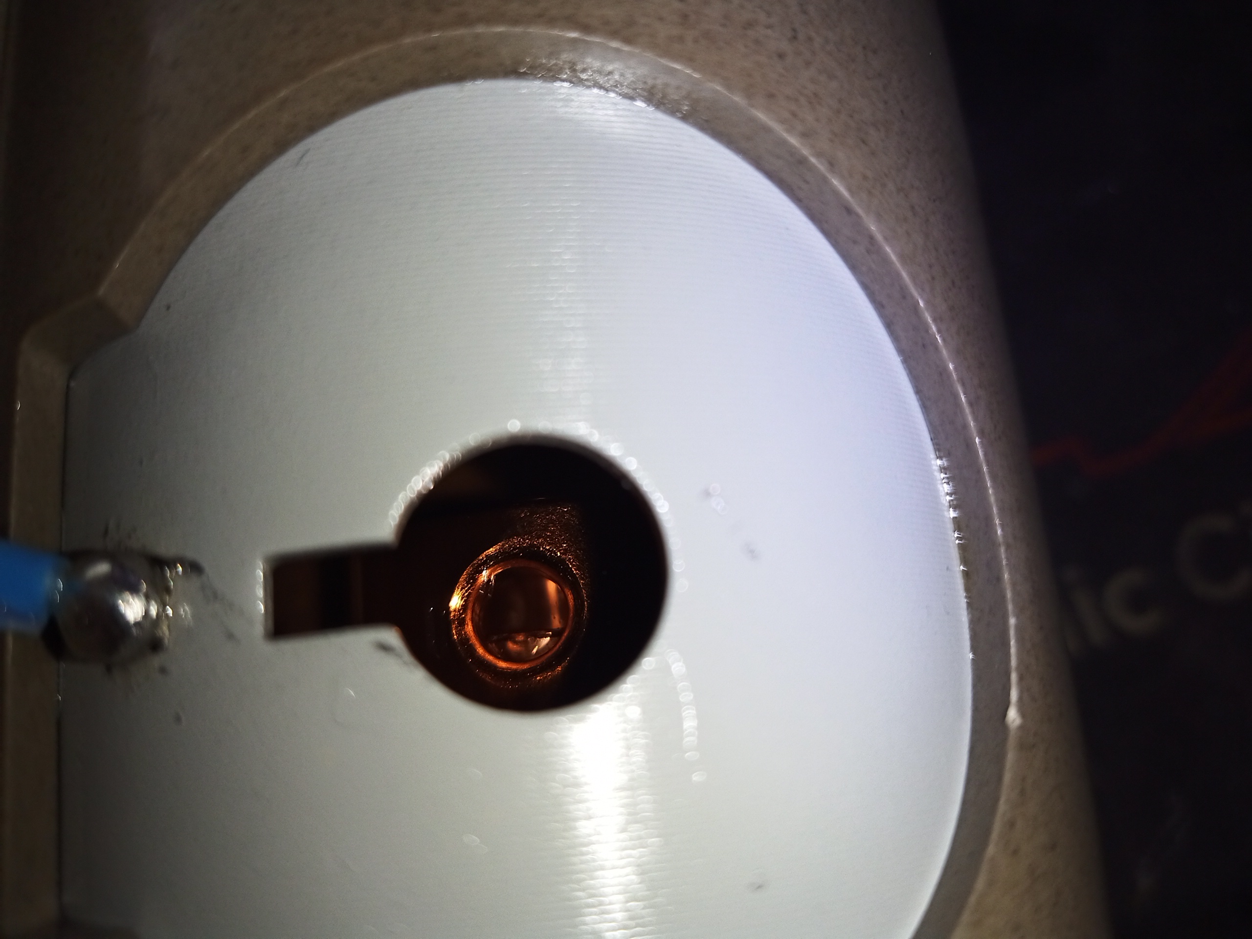
X-Ray Aperture
At the bottom of the unit is the aperture where the X-Rays emerge. The connection to the centre of the voltage multiplier is also visible here.
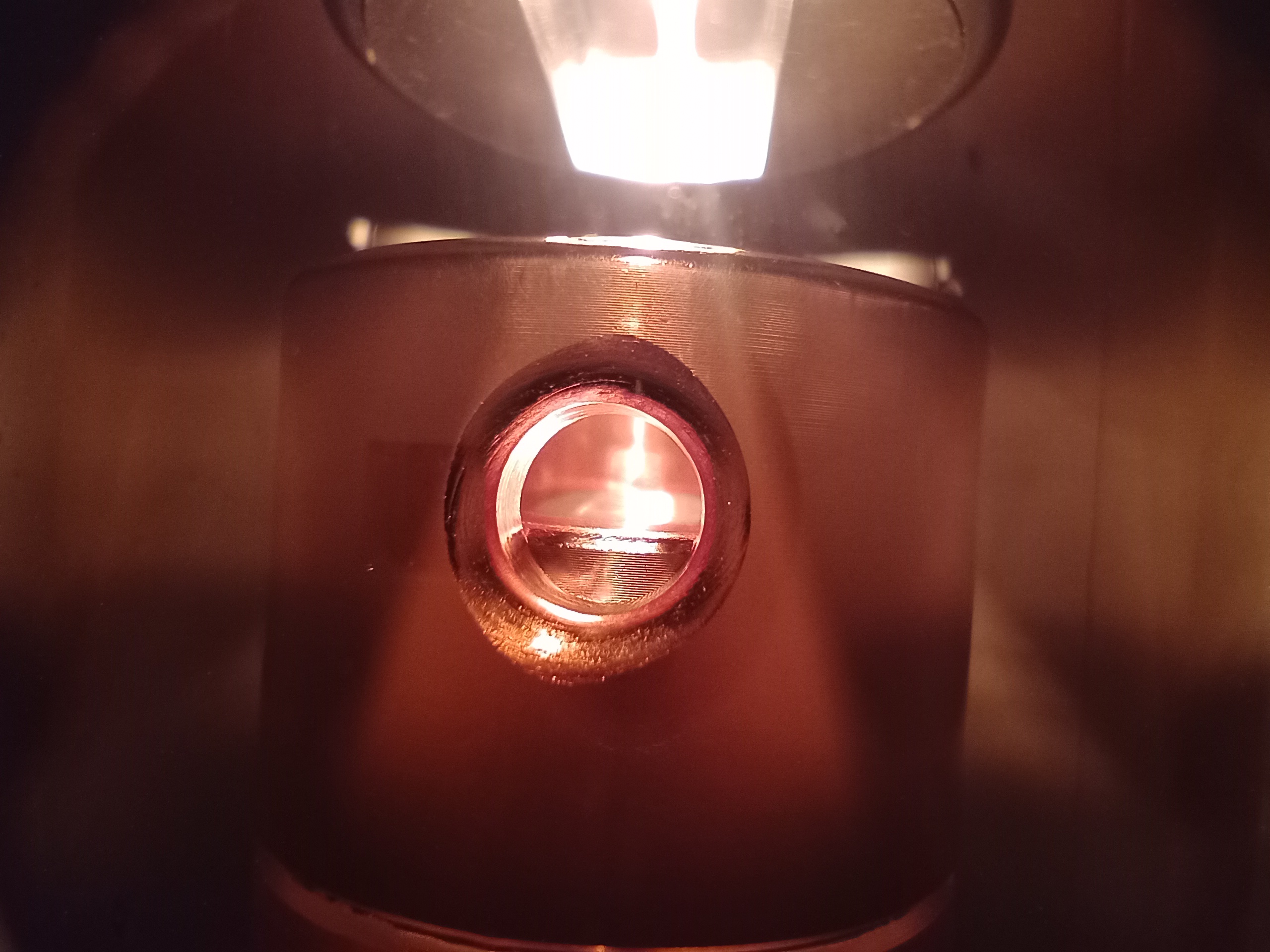
Filament Powered
Here is the view through the side of the tube with the filament powered at 4v. Filament current is about 2.6A. The copper heatsink block surrounding the Tungsten target is visible in the centre of the picture. The target is probably alloyed with Rhenium to give better longevity.
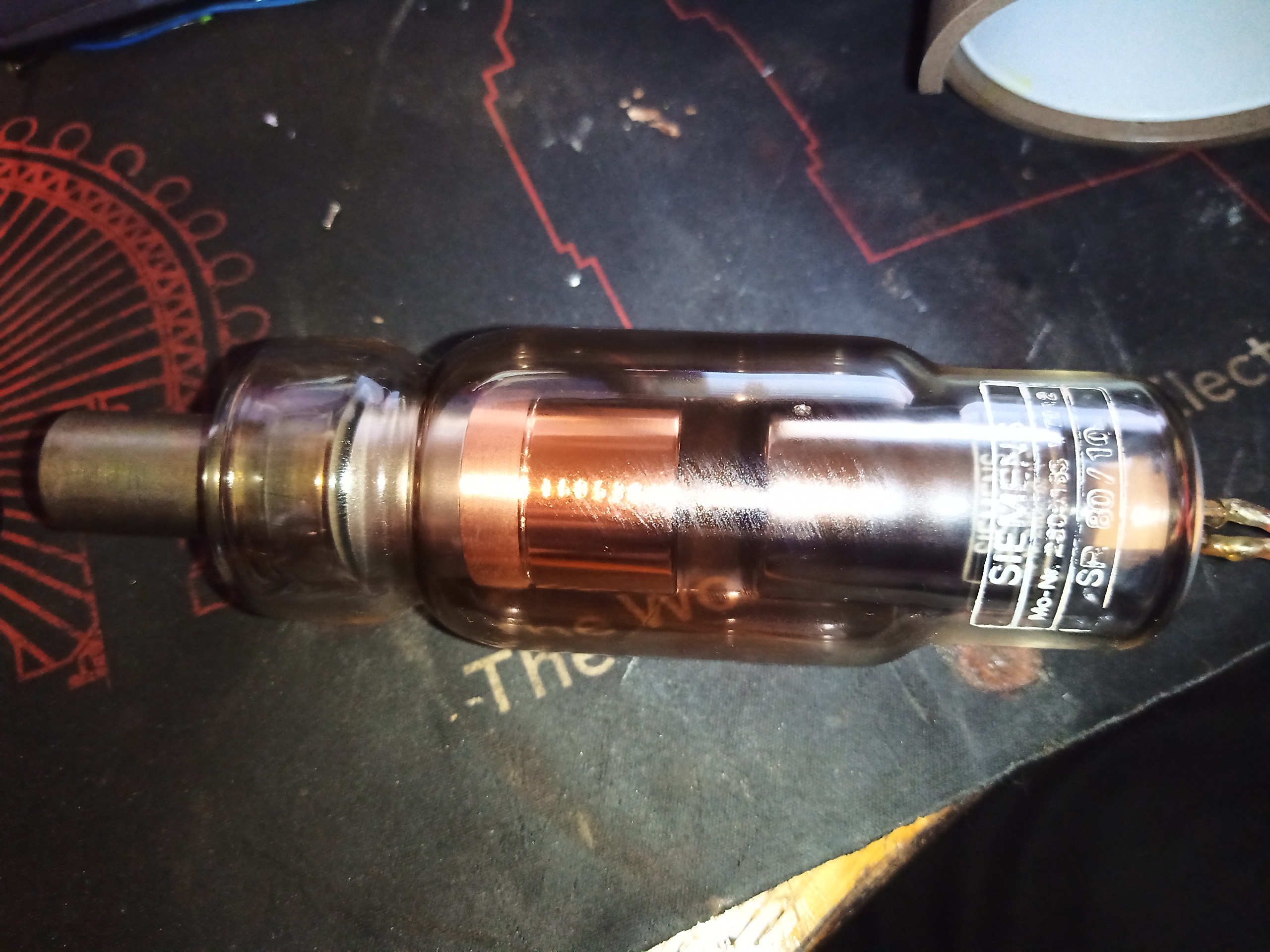
X-Ray Tube
The tube is held into the frame by a single bolt in the middle of the anode spider. Removing this bolt allows the tube to come out, and it’s heavy. This is not that surprising, since the anode of the tube is a solid chunk of Tungsten & copper!
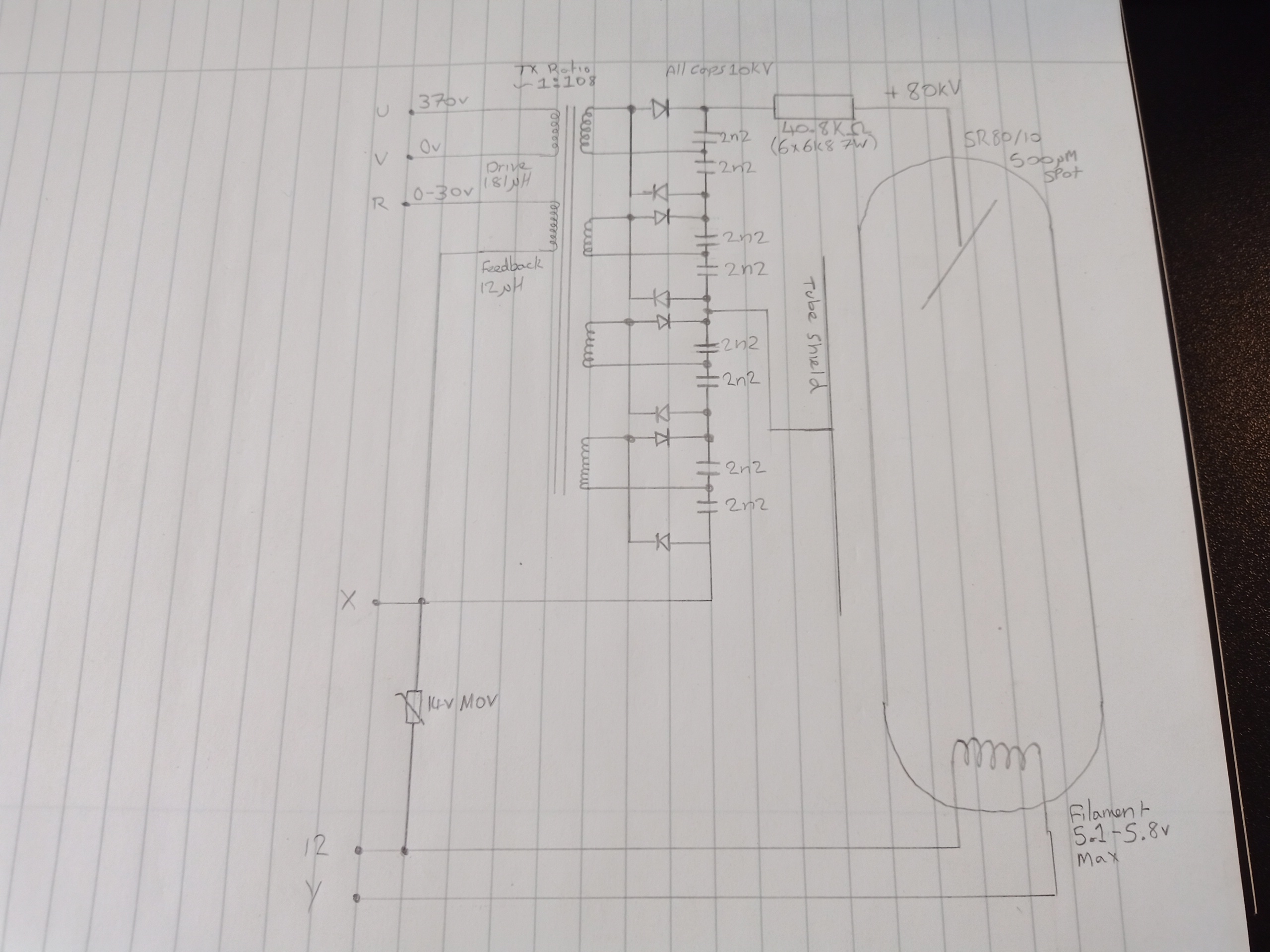
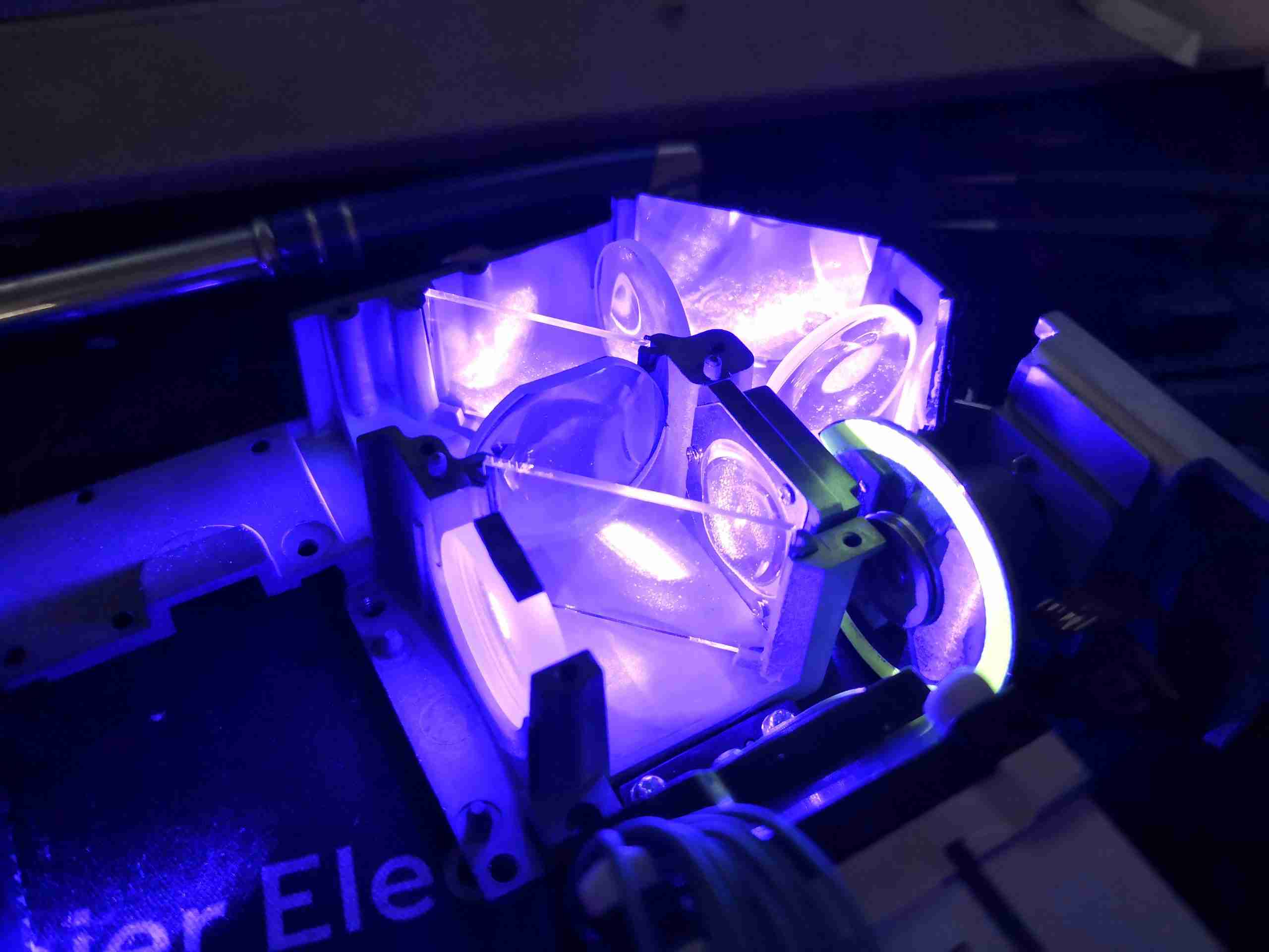
Orthophos 3 Head Schematic
Finally, here is the internal schematic of the head itself, with the pinout marked. The operating frequency of the transformer is 35kHz, and it is my understanding that these are operated in resonant mode. There’s no filament transformer, the drive for this is supplied externally. Output voltage feedback is via an auxiliary winding on the transformer.
A while back I found myself in the need of an adjustable RF attenuator capable of high-GHz operation. As luck would have it I had an old Spectrum analyser on the shelf at work, which we had retired quite some time ago.
Spectrum analysers being quite capable test instruments, I knew that the input attenuation would be done with a standalone module that we could recover for reuse without too much trouble.
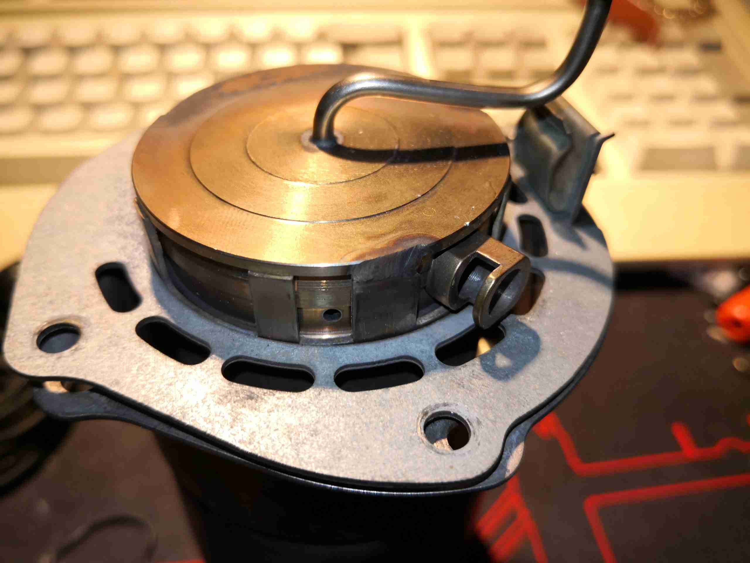
The attenuator module
Here’s the module itself, with the factory drive PCB removed from the bottom, showing the solenoids that operate the RF switches. There are test wires attached to them here to work out which solenoid switches which attenuation stage. In the case of this module, there are switches for the following:
Input select switch
AC/DC coupling
-5dB
-10dB
-20dB
-40dB
For me this means I have up to -75dB attenuation in 5dB steps, with optional switchable A-B input & either AC or DC coupling.
Drive is easy, requiring a pulse on the solenoid coil to switch over, the polarity depending on which way the switch is going.
Building a Control Board
Now I’ve identified that the module was reusable, it was time to spin up a board to integrate all the features we needed:
Onboard battery power
Pushbutton operation
Indication of current attenuation level
The partially populated board is shown at right, with an Arduino microcontroller for main control, 18650 battery socket on the right, and control buttons in the centre. The OLED display module for showing the current attenuation level & battery voltage level is missing at the moment, but it’s clear where this goes.
As there weren’t enough GPIO pins for everything on the Arduino, a Microchip MC23017 16-Bit I/O expander, which is controlled via an I²C bus. This is convenient since I’m already using I²C for the onboard display.
Driving the Solenoids
A closer view of the board shows the trip of dual H-Bridge drivers on the board, which will soon be hidden underneath the attenuator block. These are LB1836M parts from ON Semiconductor. Each chip drives a pair of solenoids.
Power Supplies
The bottom of the board has all the power control circuitry, which are modularised for ease of production. There’s a Lithium charge & protection module for the 18650 onboard cell, along with a boost converter to give the ~9v rail required to operate the attenuator solenoids. While they would switch at 5v, the results were not reliable.
Finishing off
A bit more time later, some suitable firmware has been written for the Arduino, and the attenuator block is fitted onto the PCB. The onboard OLED nicely shows the current attenuation level, battery level & which input is selected.
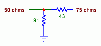
Recently I found the need to do some measurements on 75Ω CATV equipment, only having 50Ω test equipment to use. For this, matching networks exist to convert 50Ω to 75Ω, but they’re fairly simple, so building them was a viable option.
Matching Pad Schematic
Above is the very simple schematic to create the 75Ω match. To help keep any parasitics down, this circuit will be built directly onto the back of BNC connectors, that are soldered back-to-back, before being covered in shielding tape.
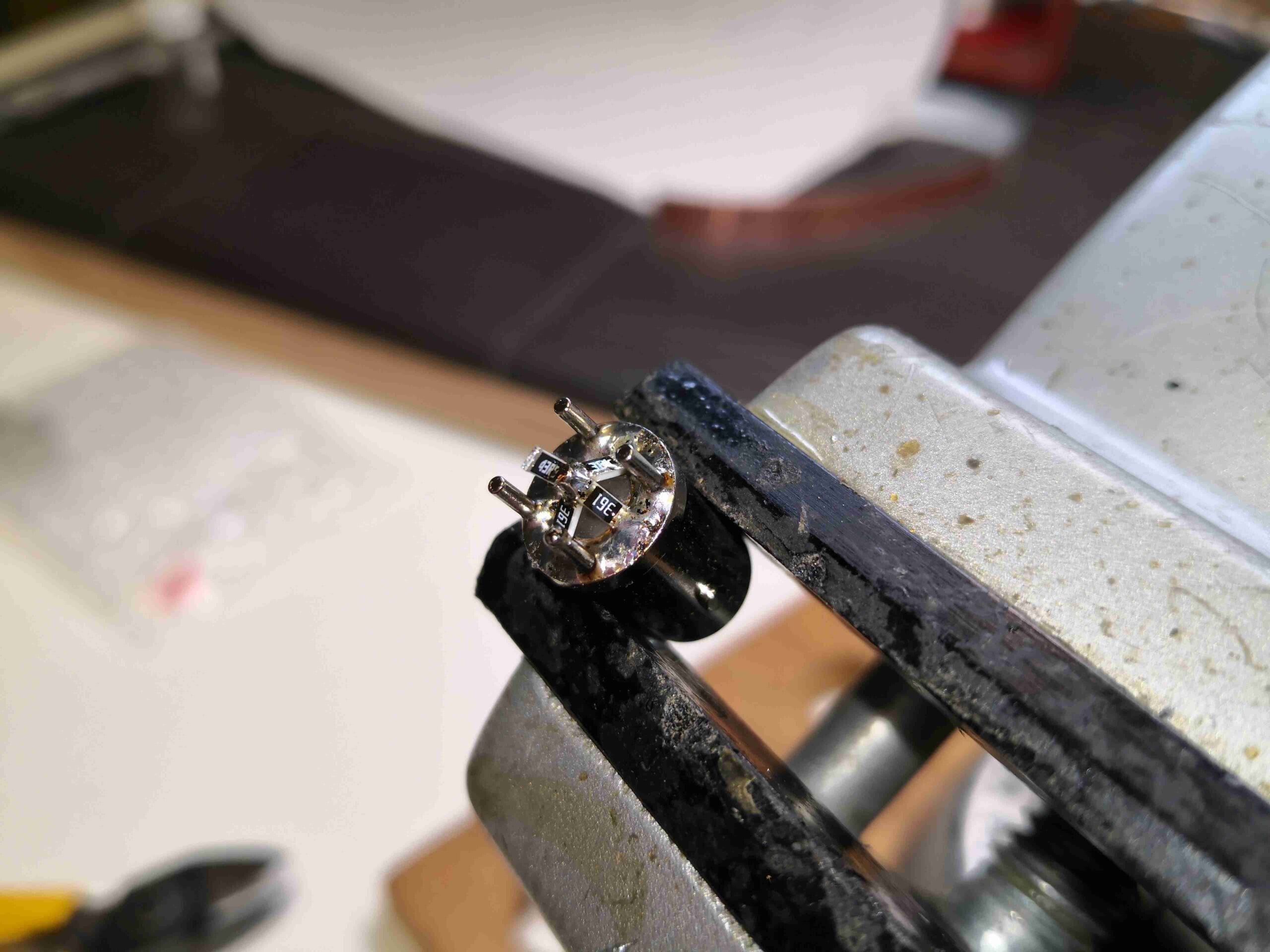
Resistors Soldered
Here’s the first 50Ω BNC connector, with the resistor network soldered on. I’ve used 4x 360Ω resistors in parallel to create the 90Ω to ground, and a single 43Ω series resistor on the centre pin.
End View
This end view of the arrangement shows the 4 resistors evenly spaced around the centre pin & soldered to the shell.
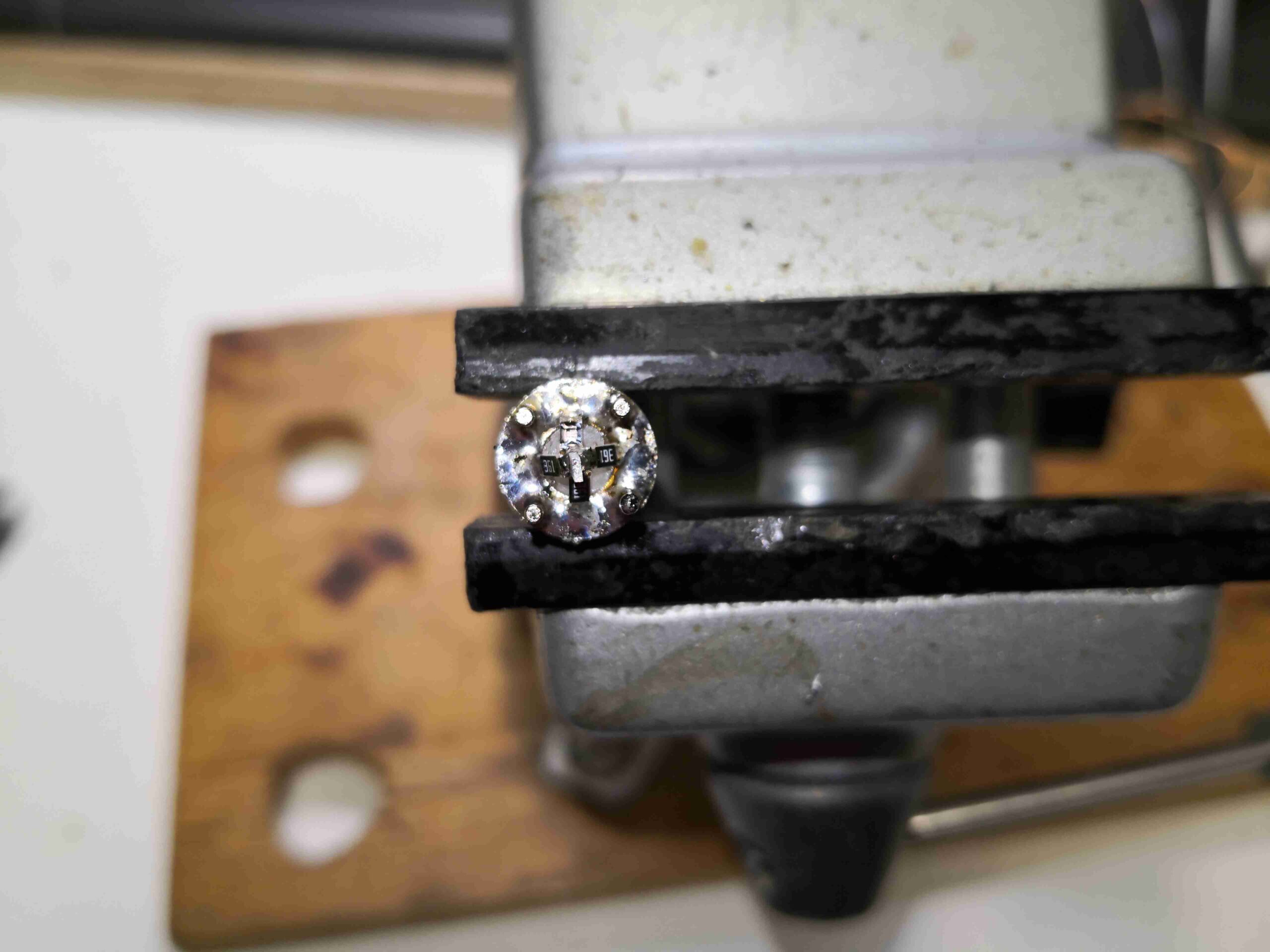
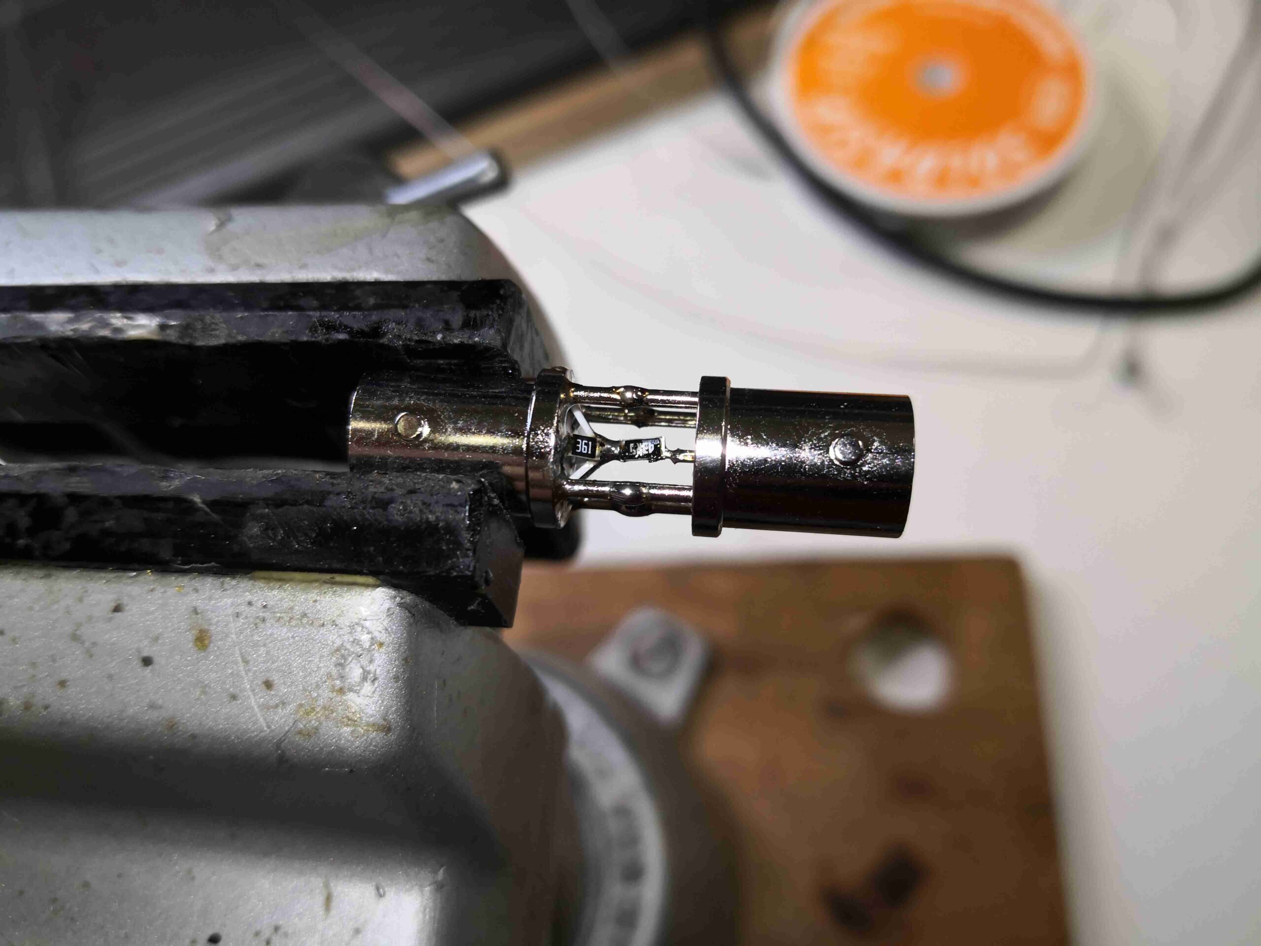
BNCs Soldered
The centre pin of the 75Ω BNC connector is trimmed down to match the length needed to touch the end of the series resistor, and it’s soldered in place. It’s a bit tricky, soldering within the gap between 2 of the ground pins!
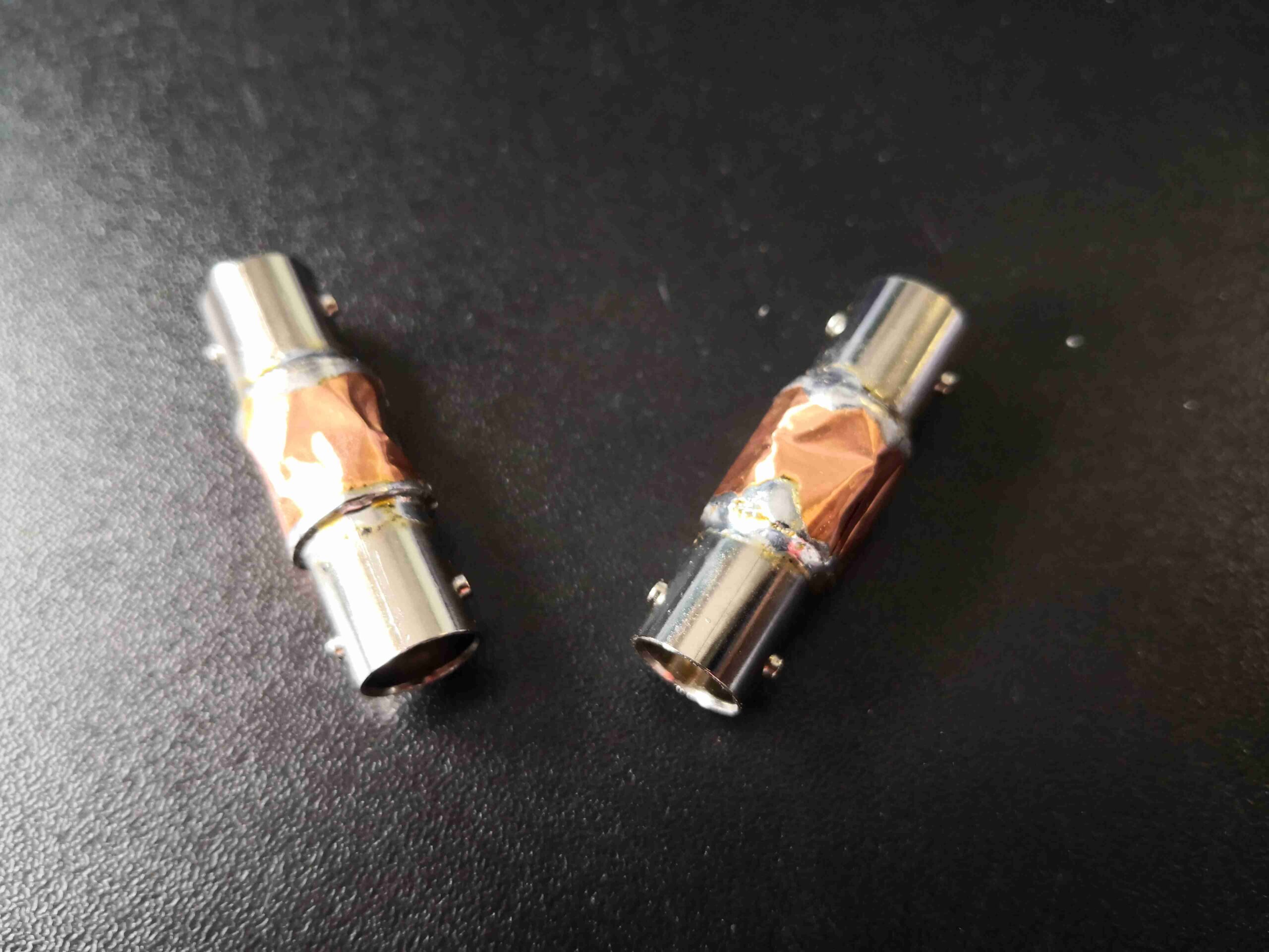
Completed Matching Pads
Finally, the internals are shielded with copper tape, soldered at the seams.
There’s a common problem with all Software Defined Radios – their input stage is wide open, and therefore susceptible to desensitisation by local high power transmitters. The main culprits are broadcasts in the FM band, from 88-108MHz. Commercial stopband filters are available to solve this issue, by cutting out the FM Broadcast band. Before I ordered a commercially produced filter, I figured I’d try my hand at building my own.
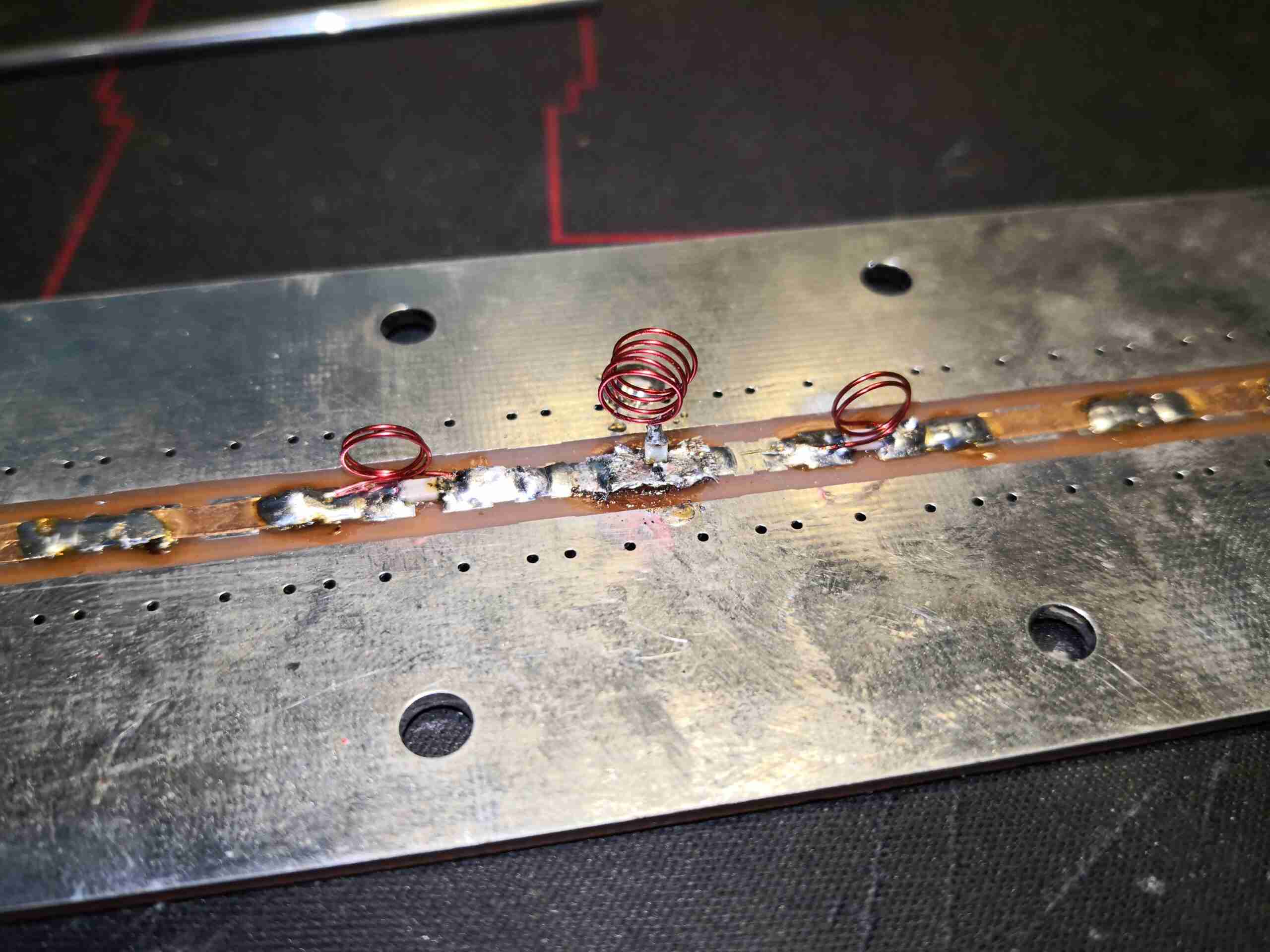
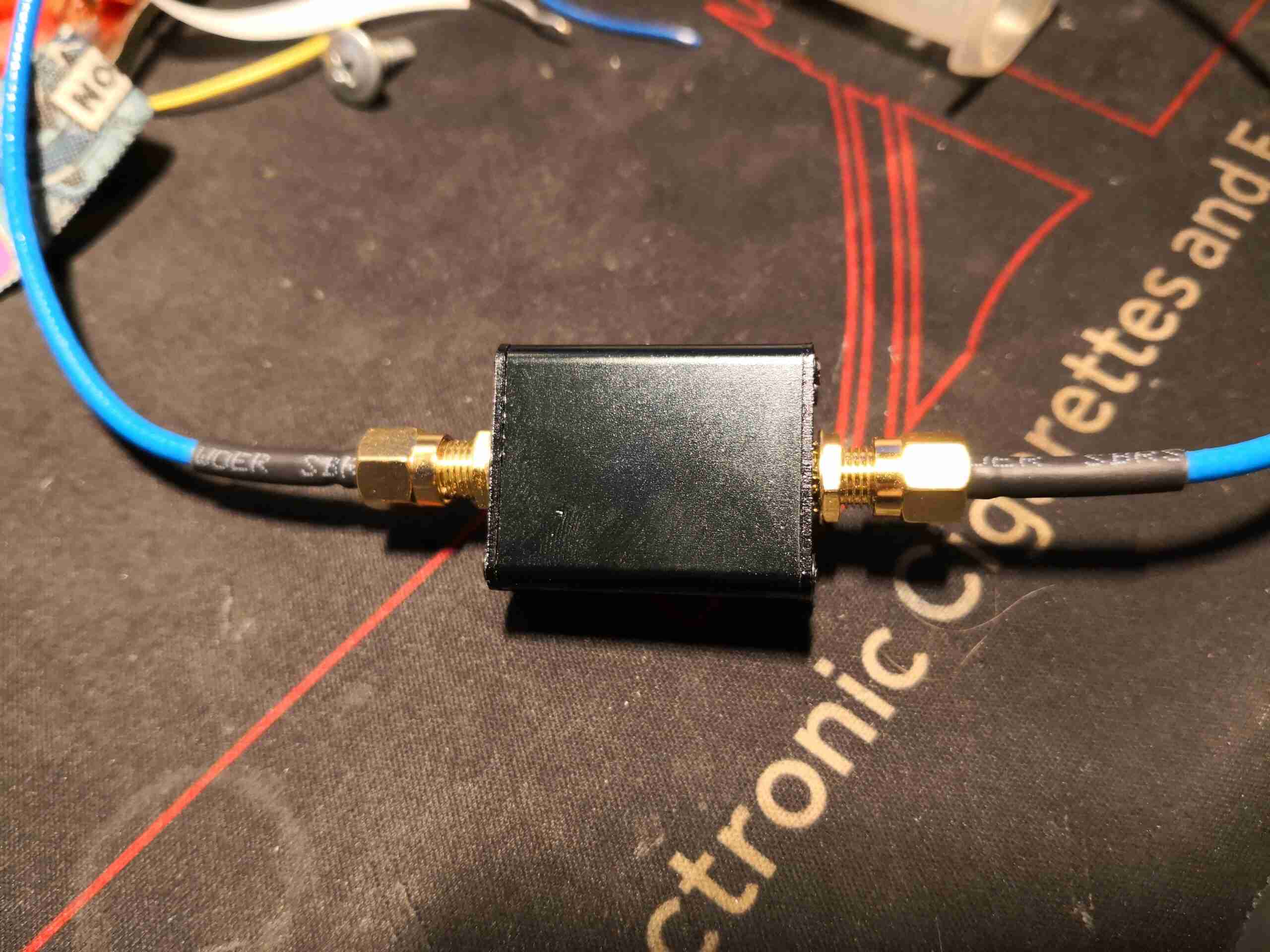
DIY Stopband Filter
Here’s the filter I came up with, a Type 2 Chebyshev. It’s built on a prototype stripline PCB, with SMA connectors at either end for I/O. This was created with the help of a filter calculator, the response of the filter can be seen below:
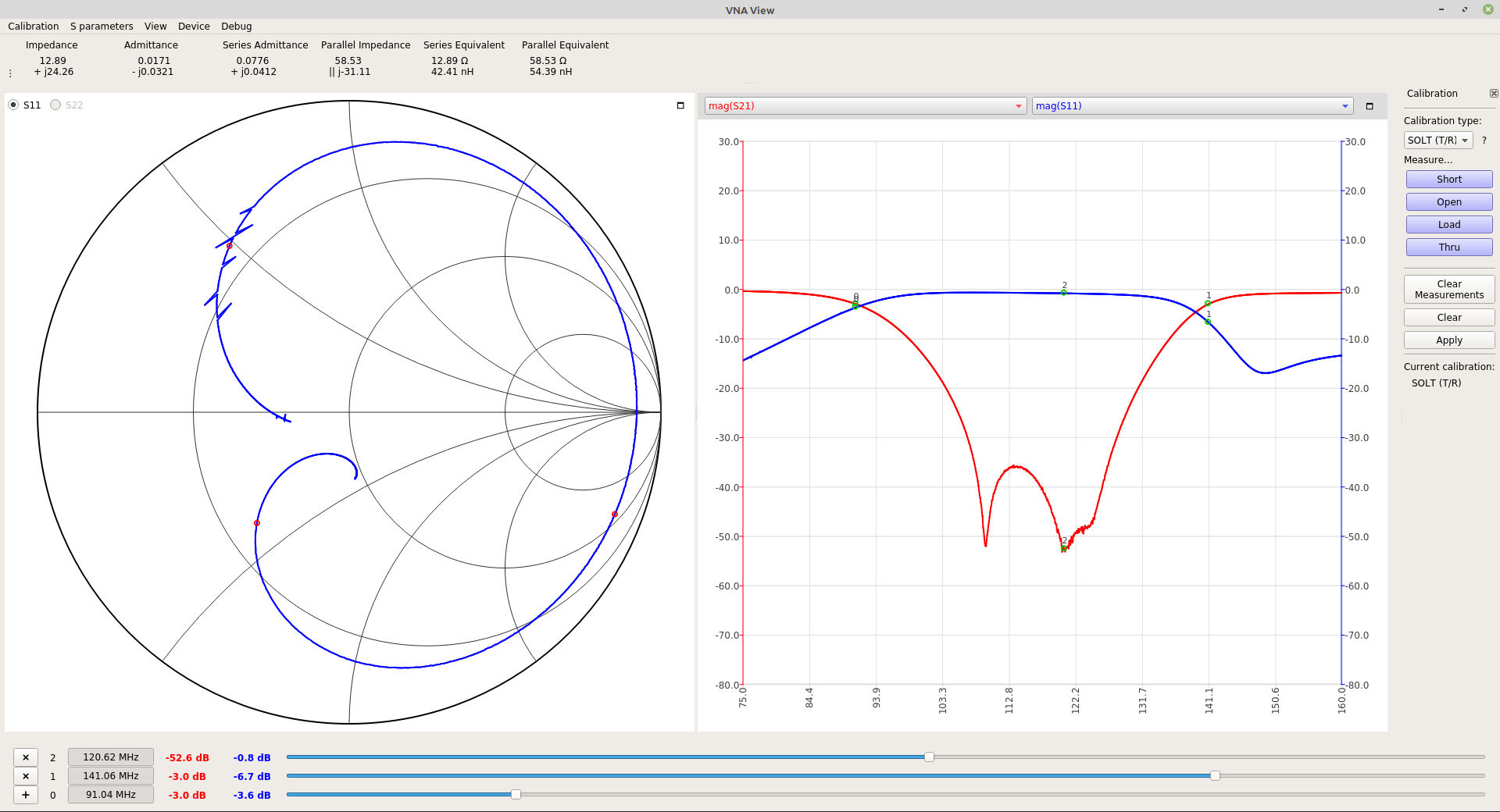
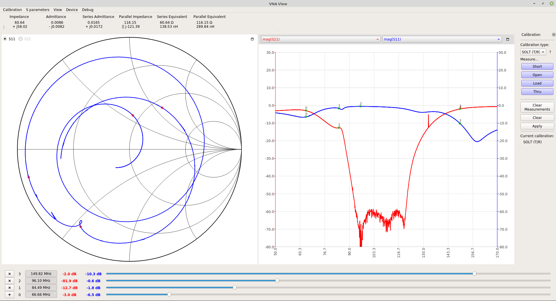
Filter VNA Performance
The response of the filter isn’t bad at all! It’s shifted up a little high on the scale, with the lower -3dB point being at 91MHz rather than 88MHz, but it does indeed chop out the broadcast band by -52dB. The high -3dB point is at 141MHz.
Let’s look at a commercial filter now, here’s the unit below, it’s definitely been size & cost optimized!
Commercial Stopband Filter
The box is tiny, not much bigger than the SMA connectors!
Commercial Filter VNA Characteristics
Looking at the plot from the NanoVNA, it’s clear this is also a Type 2 Chebyshev, but it’s more effective. This has a stopping power of -82dB, it’s also better centred.
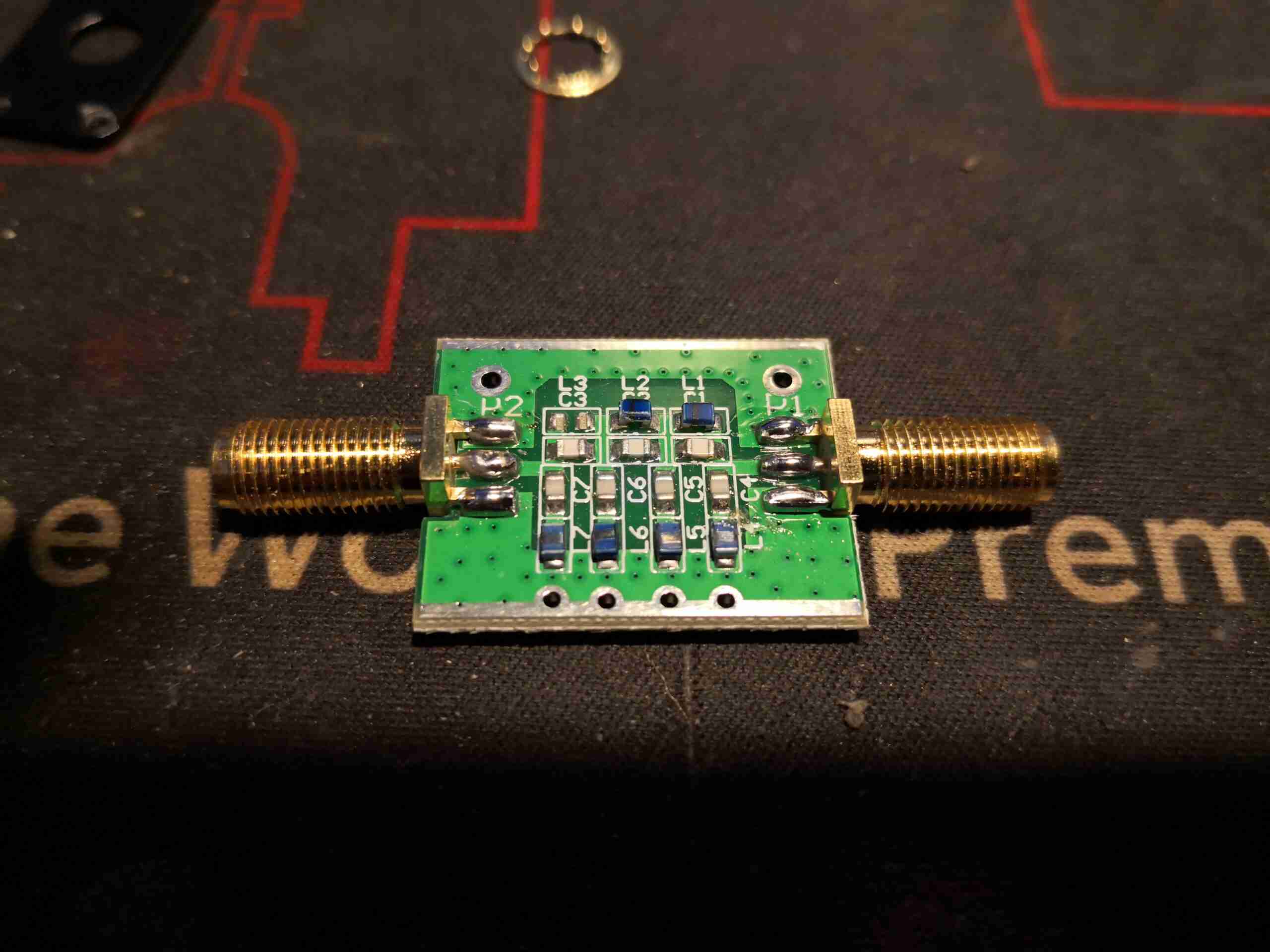
Commercial Filter PCB
The board easily removes from the external shell. The SMA connectors are edge launch, which is good for maintaining impedance. There are a couple more stages of filtering in here than I put on my filter, which explains the much improved blocking characteristics. There does appear to be some damage though – there’s an inductor missing from the left side of the PCB. This is probably responsible for the odd response at the low end. There clearly was an inductor there, as the solder fillets are still present. Maybe this was removed at the factory as a form of tuning?
There’s quite a nice desktop app for the new NanoVNA v2, NanoVNA-Qt. It’s released as an AppImage for Linux, but unfortunately there is no version to run on a Pi supplied. The version below is built to run on the latest version of Raspbian (as of writing this, 2020-05-27).
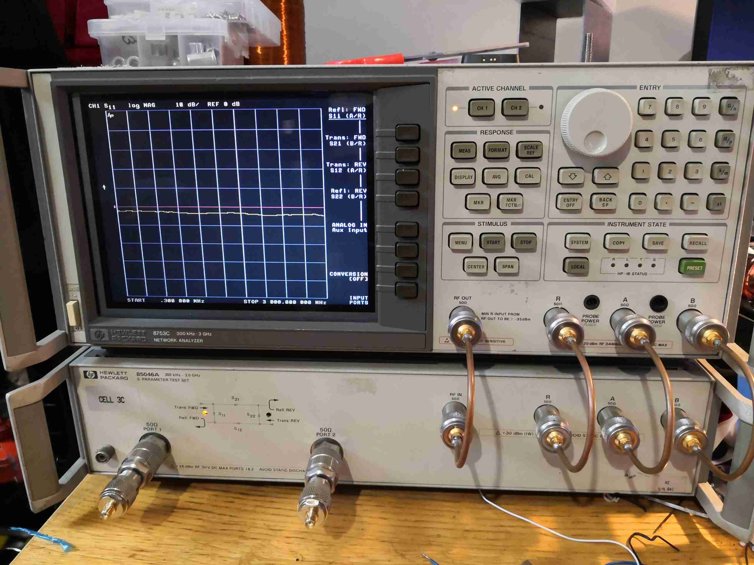
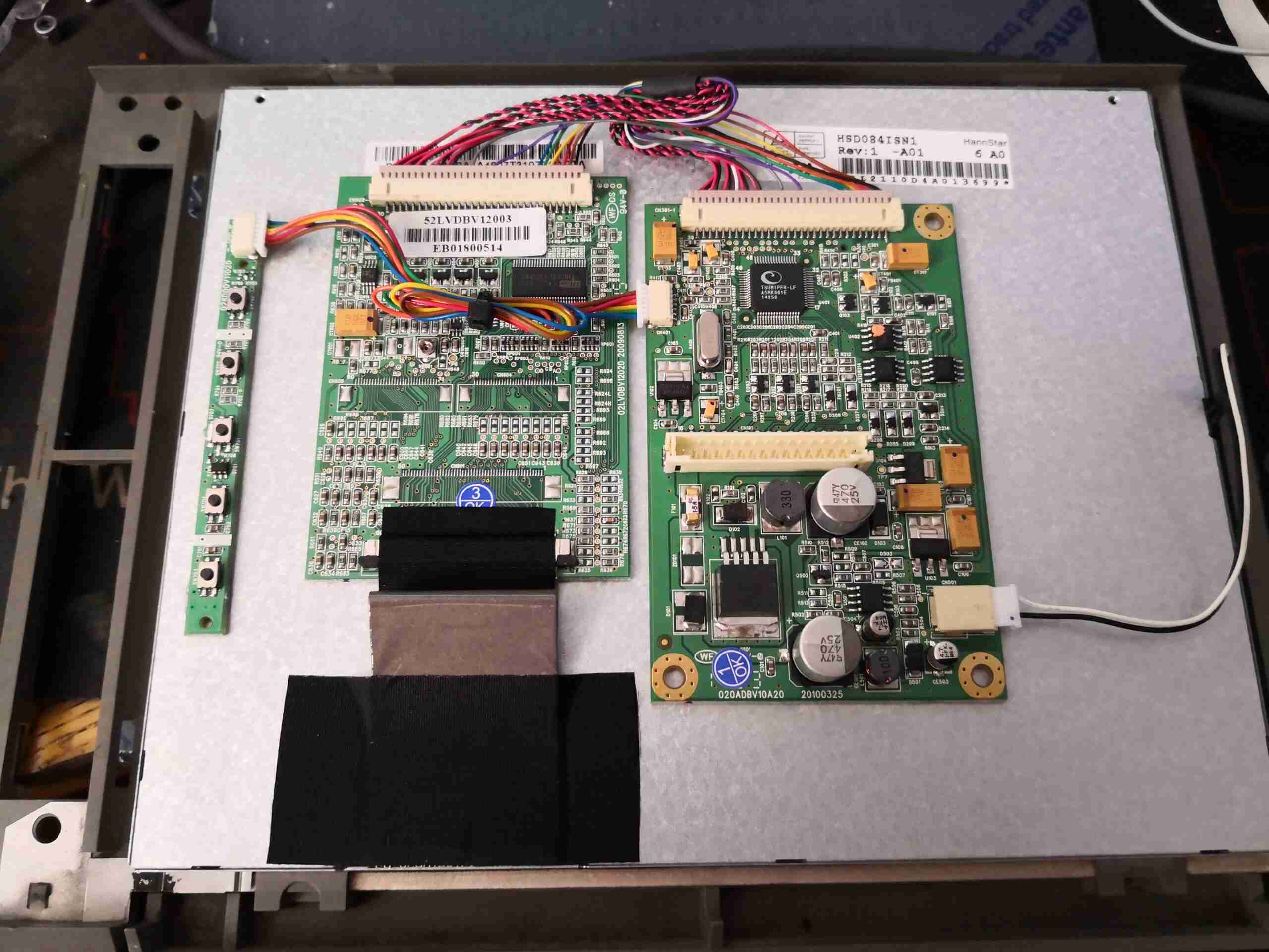
Since I inherited an old HP 8753C Network Analyser from work, I figured updating a few things to relatively modern standards would be good. The factory CRT, being 28 years old, is definitely getting a little tired, not to mention being slow to warm up. I read over on the EEVBlog forums about a DIY modification to integrate an LCD display into place instead. There was also the option of a ready-made kit for these instruments which would integrate an LCD, but the cost at over £300 was very prohibitive!
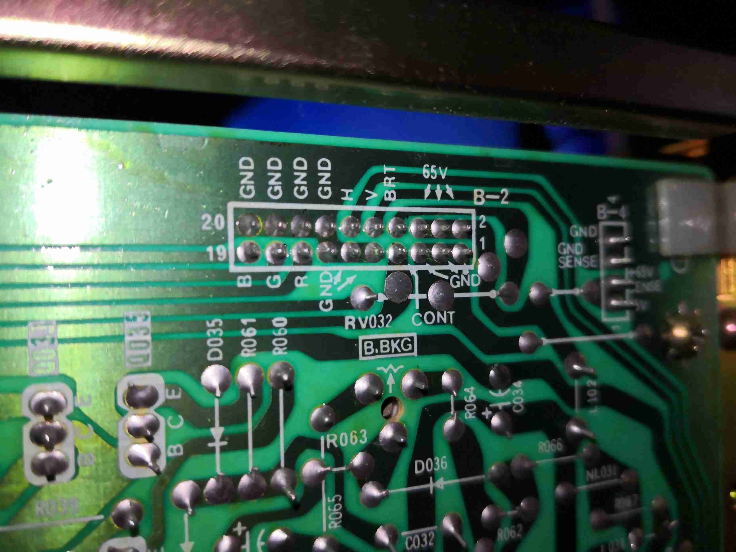
CRT Pinout
The CRT display unit is a self-contained Sony unit, taking RGBHV signalling from the graphics control card of the analyser. Power is 65v DC which will definitely come in handy for powering the new LCD & control gear, after some conversion.
Test Wiring
Doing a quick test with some wiring stuck into the video connector from the graphics controller, proved that I could get a decent video signal out of the unit! The only signals used here are RGB, along with the vertical & horizontal sync.
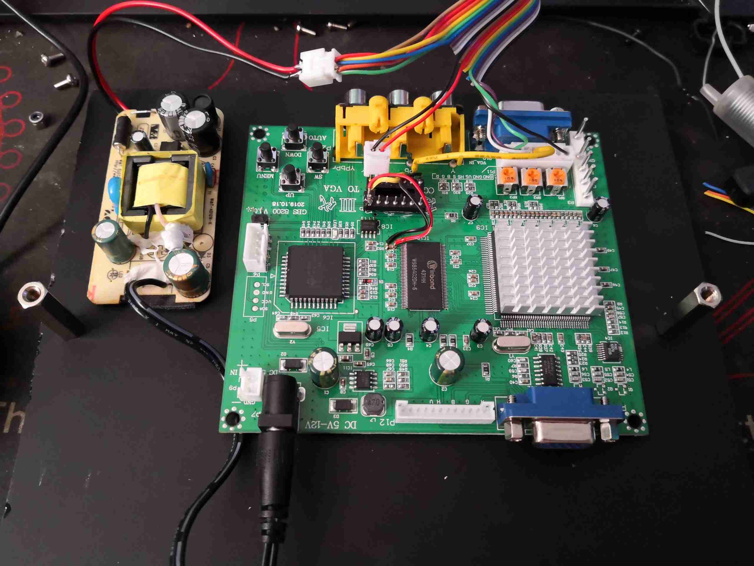
GBS-8200 Converter Board
The video is converted to VGA by way of a GBS-8200 arcade machine video conversion board, which will take many different video formats & spit out standard VGA signalling. The power supply to the left is a standard 100-240v to 12v PSU, which is happy to run at 6t5v DC input voltage, albeit with a ~5 second delay on output startup when power is applied. This is due to the massive 6.6MΩ resistance of the startup resistor chain, which I did reduce by 50% to 3.3MΩ with no effect. Since it does start OK even with the delay, I think I’ll not tinker with it any further. I doubt I could pull the full rated power from it with such a low input voltage, but all included, this mod draws less than 600mA at 12v.
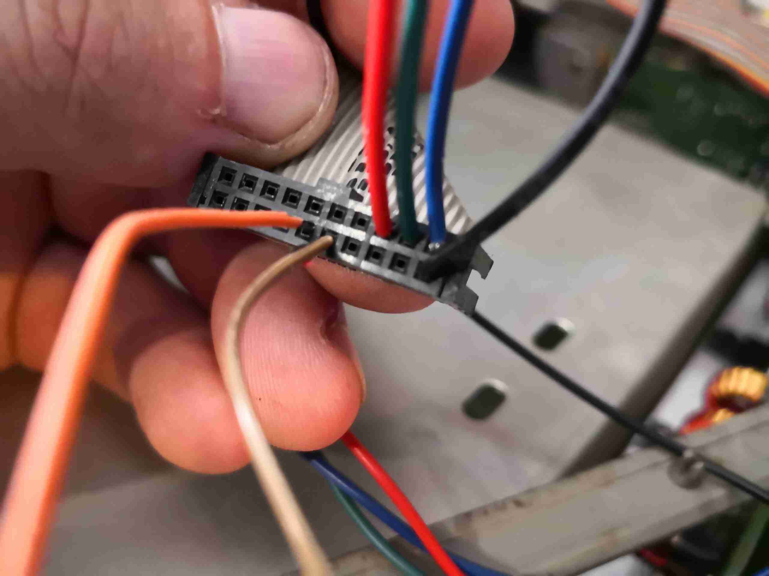
A custom 20-pin IDC cable was made up to connect to the analyser’s graphics board, and this was then broken out into the required RGB & sync signals. Quite a few of the grounds are unused, I’ve not yet noticed any issues with EMC or instability.
Sync Combiner
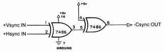
There is a quad-XOR gate deadbugged to the PCB, which is taking the separate sync signals & combining them into a composite sync. The conversion board does have separate sync inputs, but for some reason doesn’t sync when they’re applied separately. This gate IC is powered from the 3.3v rail of the converter board, with the power lines tacked across one of the decoupling caps for the DRAM IC.
LCD Control PCBs
The donor 8.4″ LCD came from eBay in the form of a POS auxiliary display. I pulled the panel from the plastic casing, along with the control boards, and attached them all to the back. This LCD also had a sheet of toughened glass attached to the front, no doubt to protect against the Great Unwashed while in use! This was also removed.
Control Boards Mounted
A cut piece of plexiglas allows the boards to be mounted in the cavernous space the CRT once occupied, with some brass standoffs. 12v power & VGA are routed down to the LCD on the front of the analyser.
LCD Wiring
The LCD itself is tacked in place with cyanoacrylate glue to the securing clips for the glass front panel, which is more than enough to hold things in place. The input board which just has the VGA connector & power connector is glued edge-on to the metal back panel of the LCD, and is under little strain so this joint should survive OK.
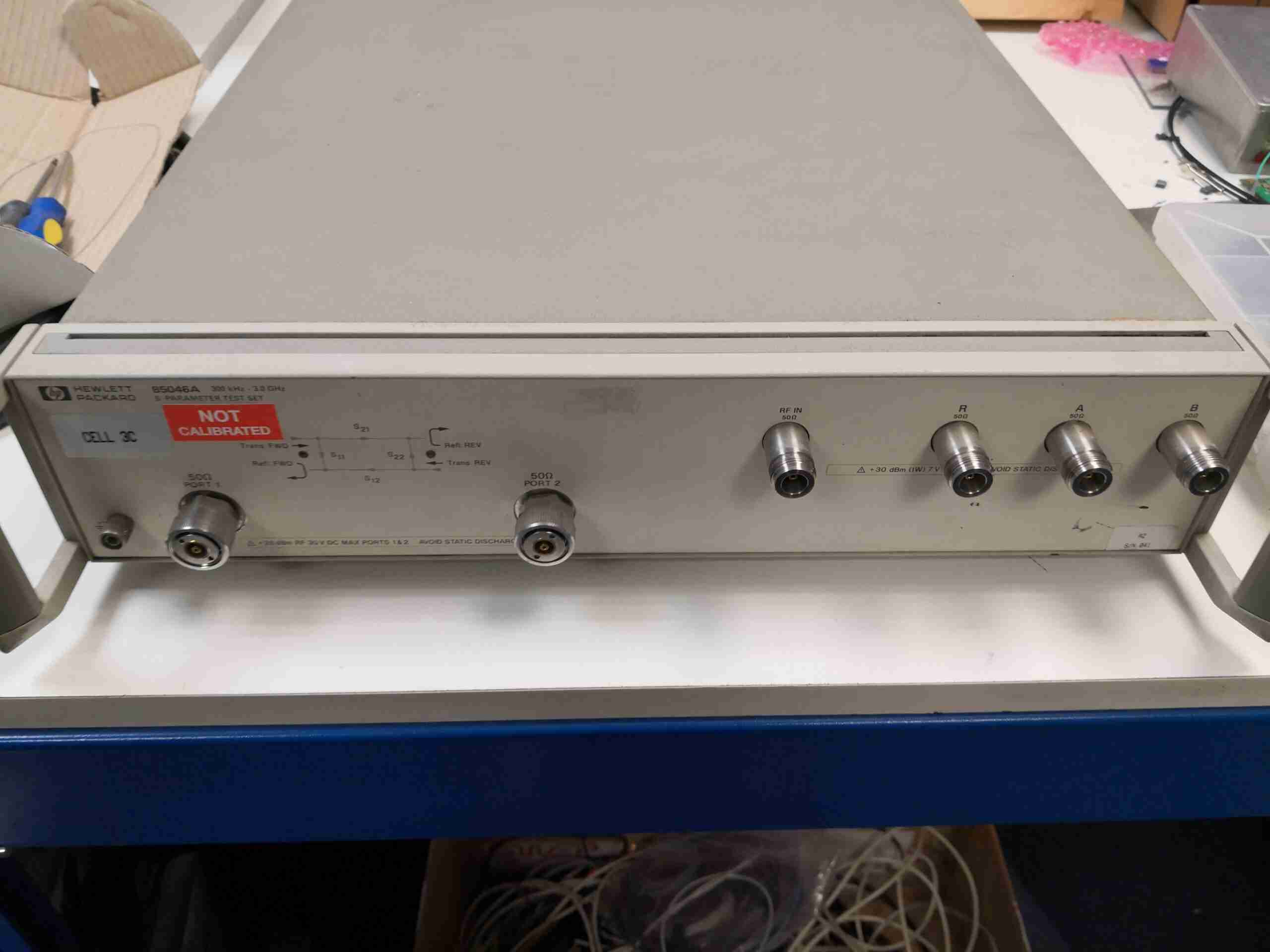
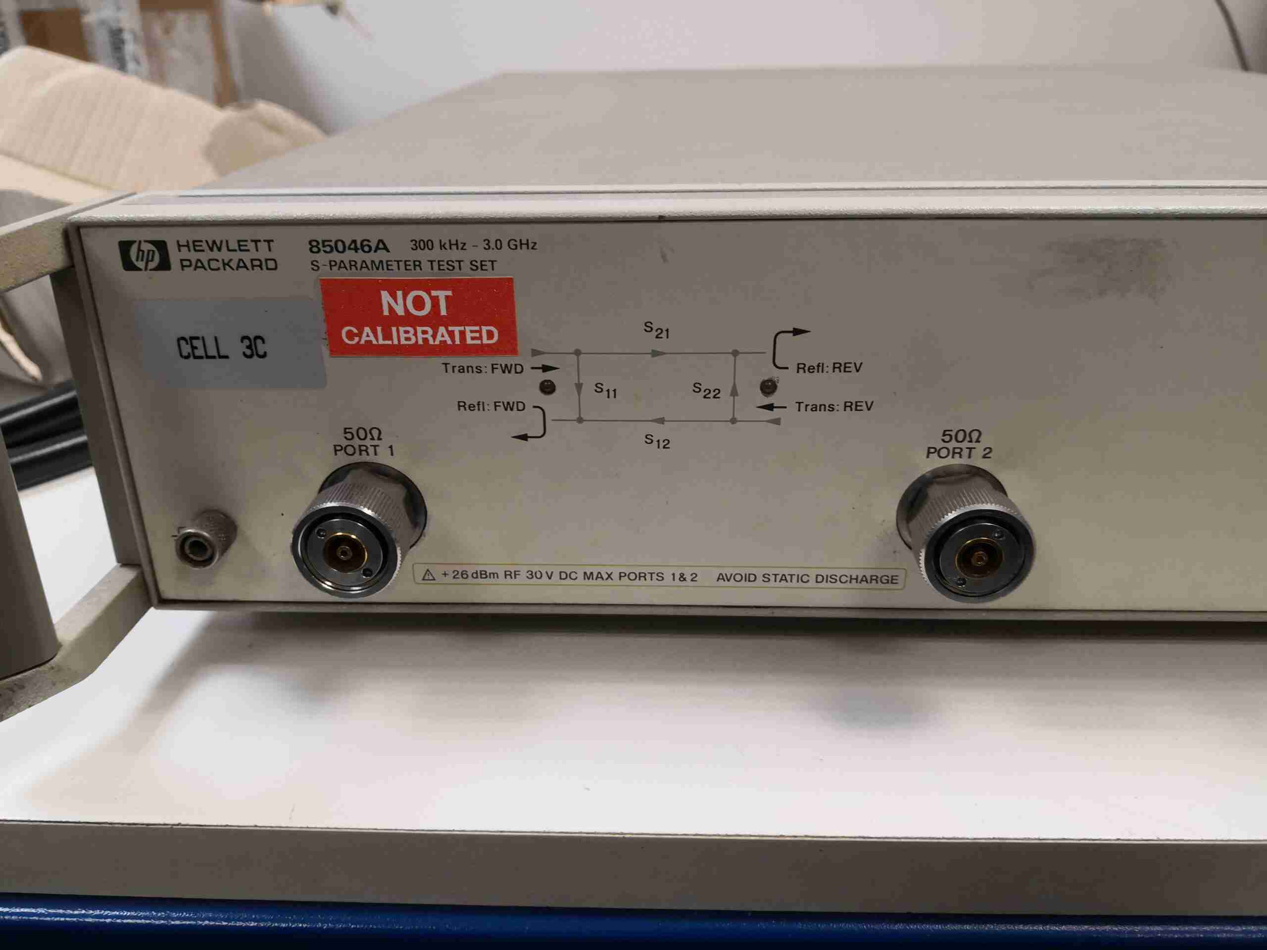
This enormous box is the S-Parameter Test Set from a HP 8753C 3GHz network analyser. This unit contains the required components to automate the testing process for items such as cables, antennas & RF networks.
7mm Test Ports
The main EUT test ports are APC-7mm type connectors – a very expensive genderless RF connector that provides very repeatable coaxial connections.
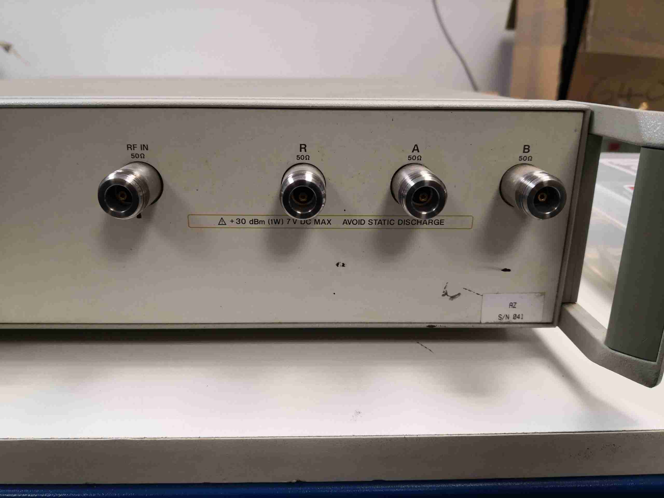
N-Type Analyser Interconnects
The interconnects for the RF input, Reference output back to the analyser, A&B ports are N-Type, and should be connected to the main unit with phase-matched cables.
Lid Removed
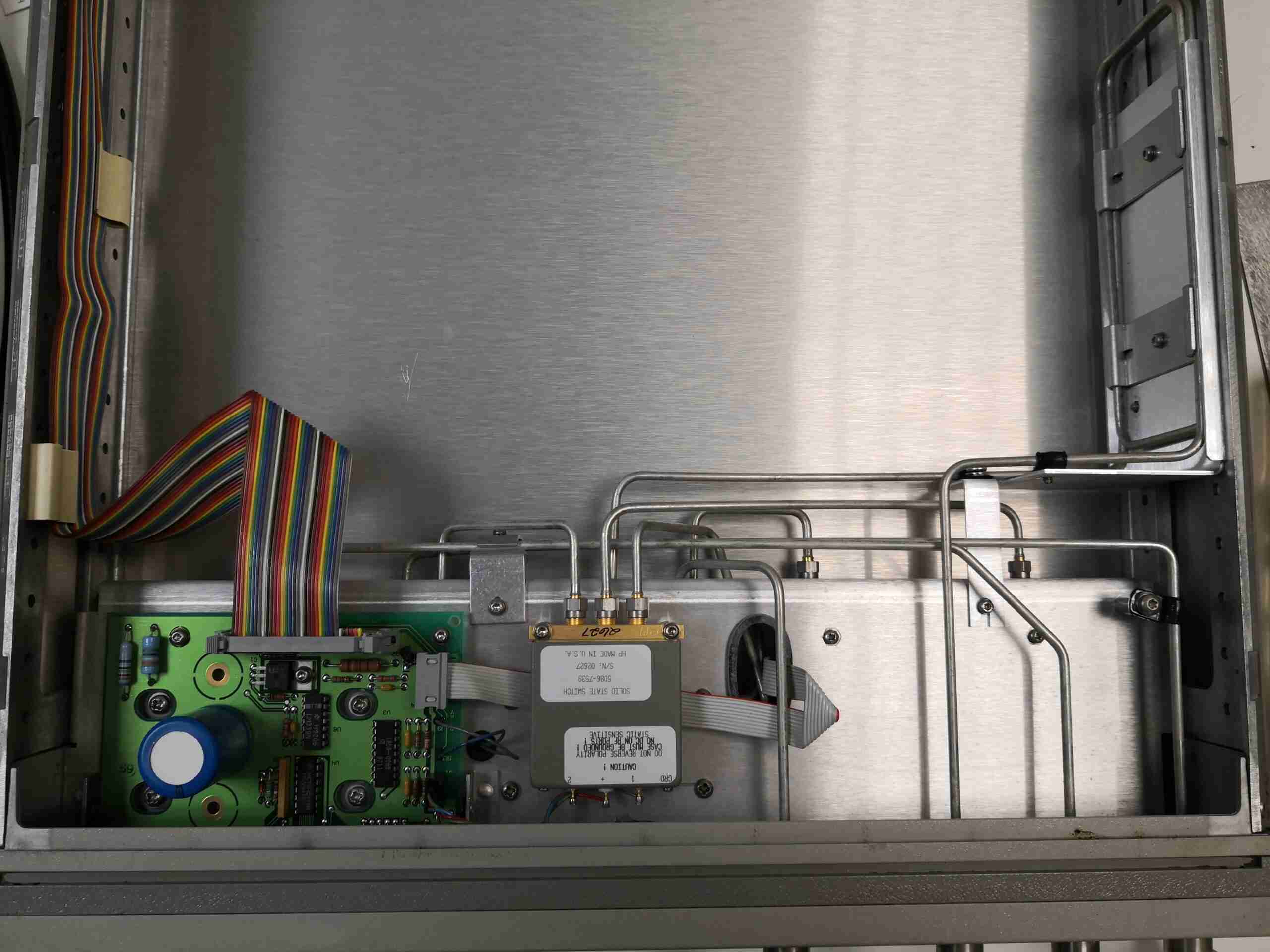
On removing the lid, it’s almost a completely empty box! All the RF magic is done in the first 150mm behind the front pane, apart from a coil of semi-rigid coax on the right, which will be to match the lengths of cables in the unit for phase purposes. There’s not much visible on the top here, just the control board, which takes signalling from the main analyser unit, and only has some glue logic & comparators. There’s a very nice 3-port solid-state RF switch in the centre, for switching between S12 & S21 measurements rapidly, a function that would not be possible with a mechanical relay. All the internal connections are made with semi-rigid coaxial cable, fitted with SMA connectors.
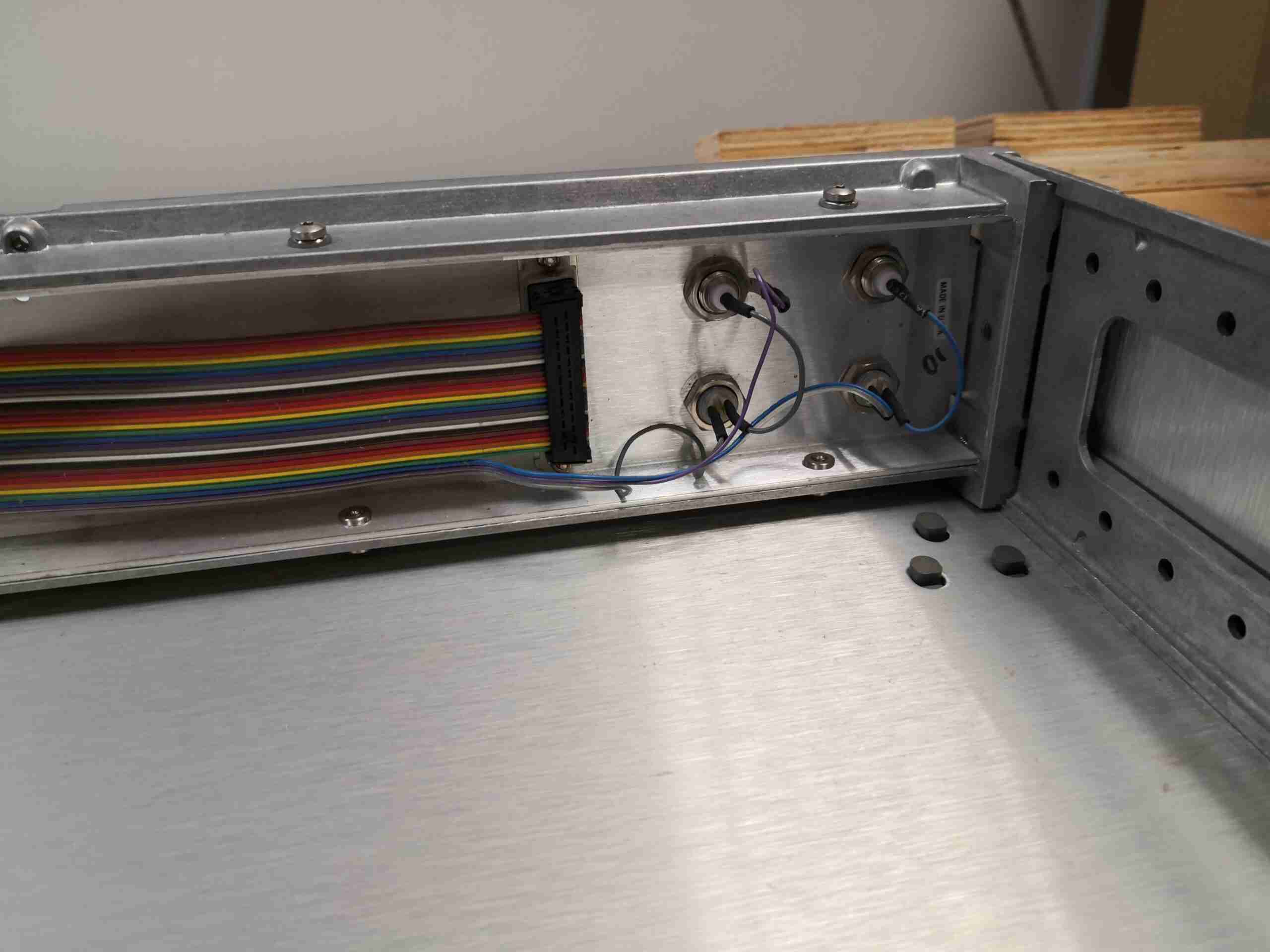
Rear Panel Connections
The back of the case just has the 25-way D connector for control, and a pair of BNC connections & 500mA fuses for DC biasing the output ports where required by the EUT.
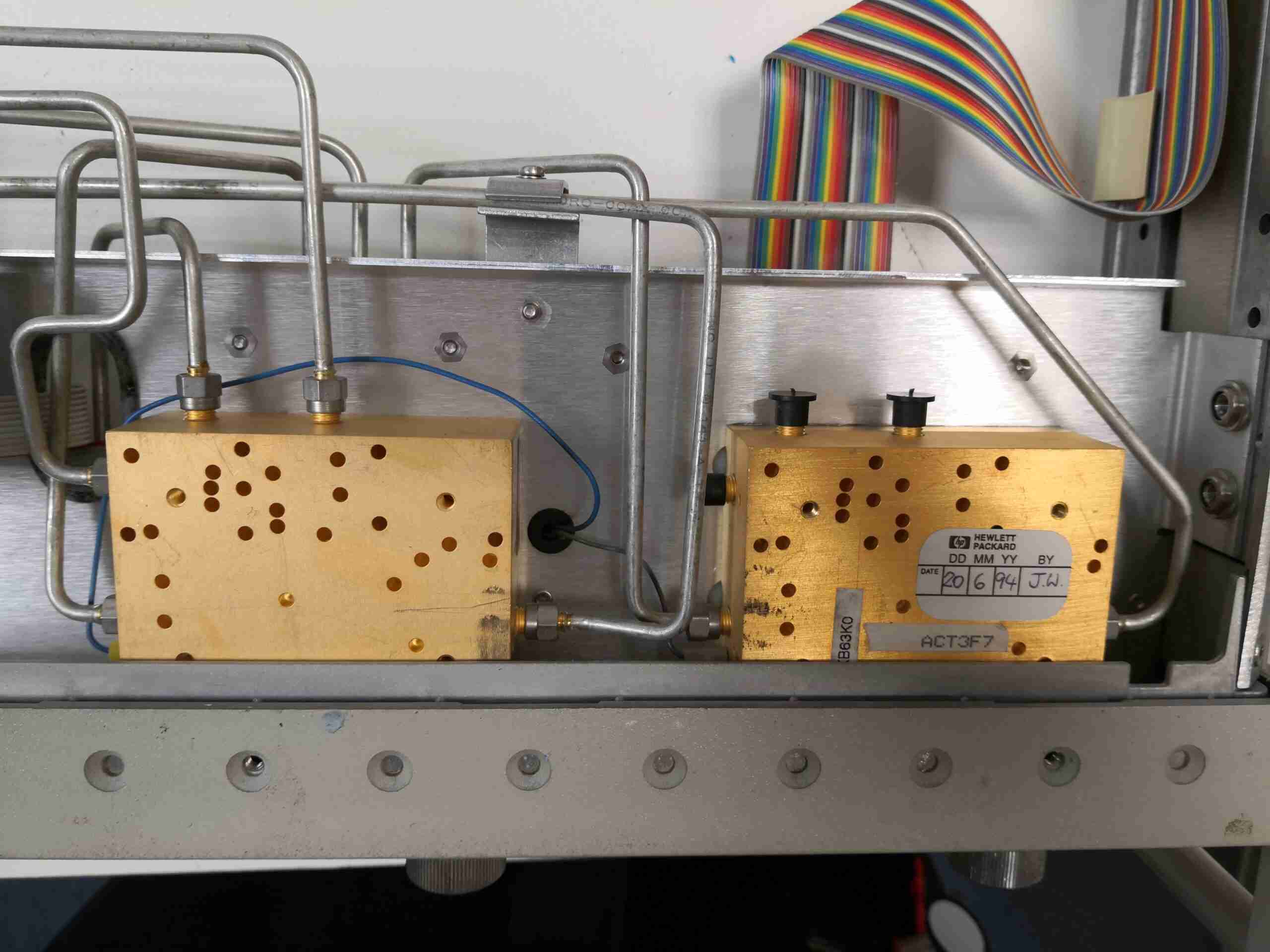
Power Splitter & Directional Couplers
Underneath the centre panel is where most of the RF magic happens. These two blocks, which are integrated with the test ports contain bias tees for each port, a power splitter for the RF reference back to the analyser & directional couplers for reading back the forward & reverse RF power from each test port.
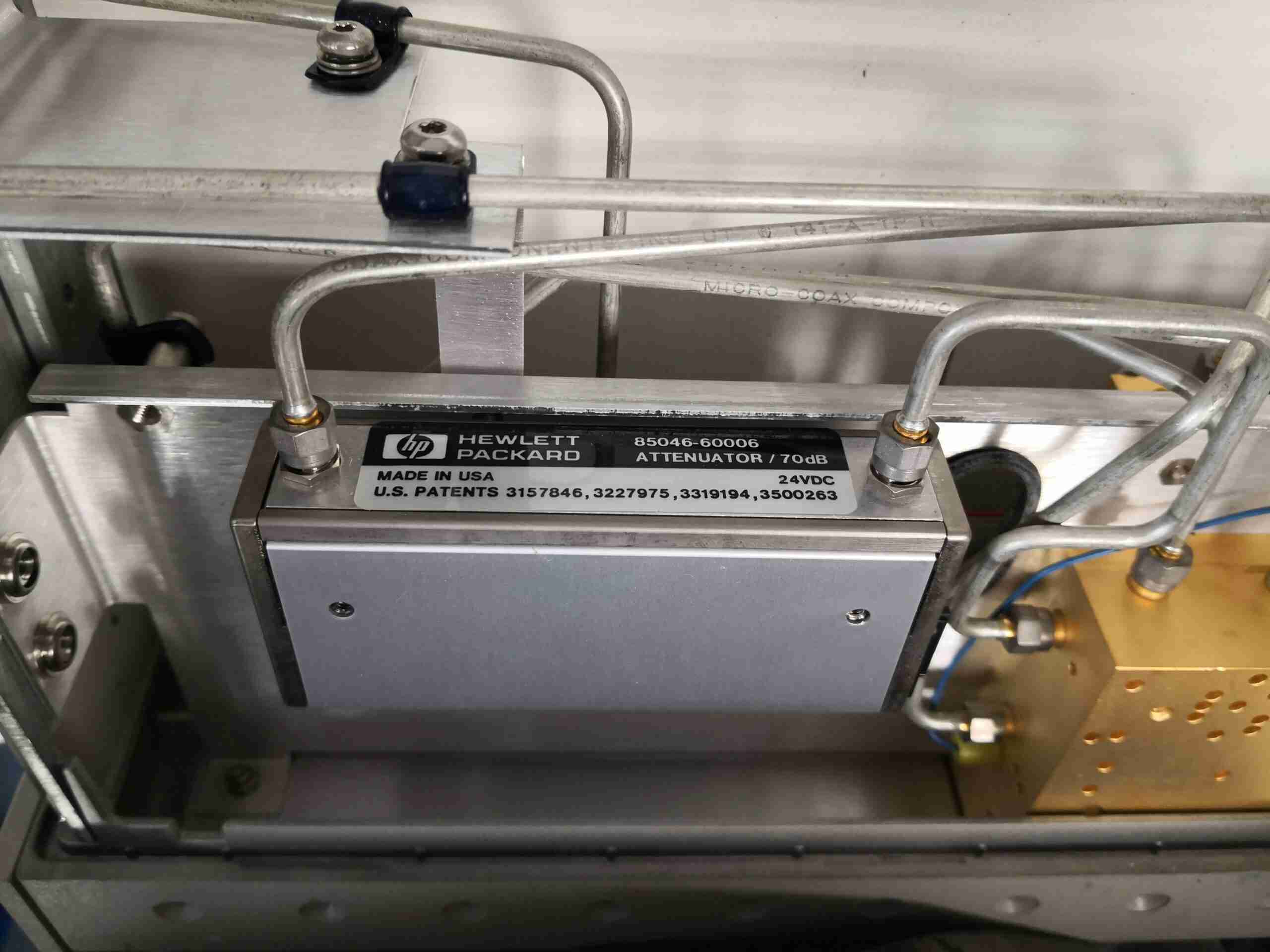
Step Attenuator
The final component in here is a 70dB step attenuator, adjustable in 10dB steps.
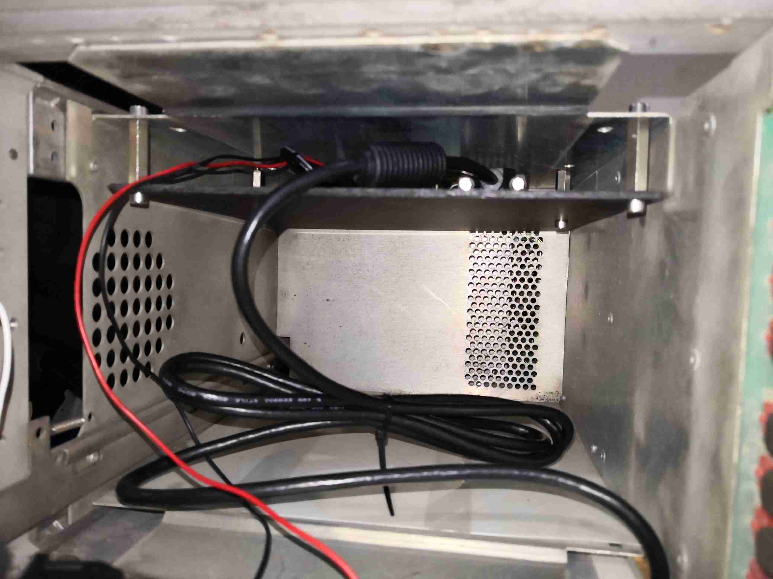
Since I fitted the new “8kW” diesel heater to the camping power trolley, it has occurred to me that there is a lot of energy in the exhaust gas stream that ordinarily would be wasted into the atmosphere. Since we’re all still on lockdown here in the UK, I figured it would be good to run an experiment to see if it was worth recovering this energy – in the form of heating water.
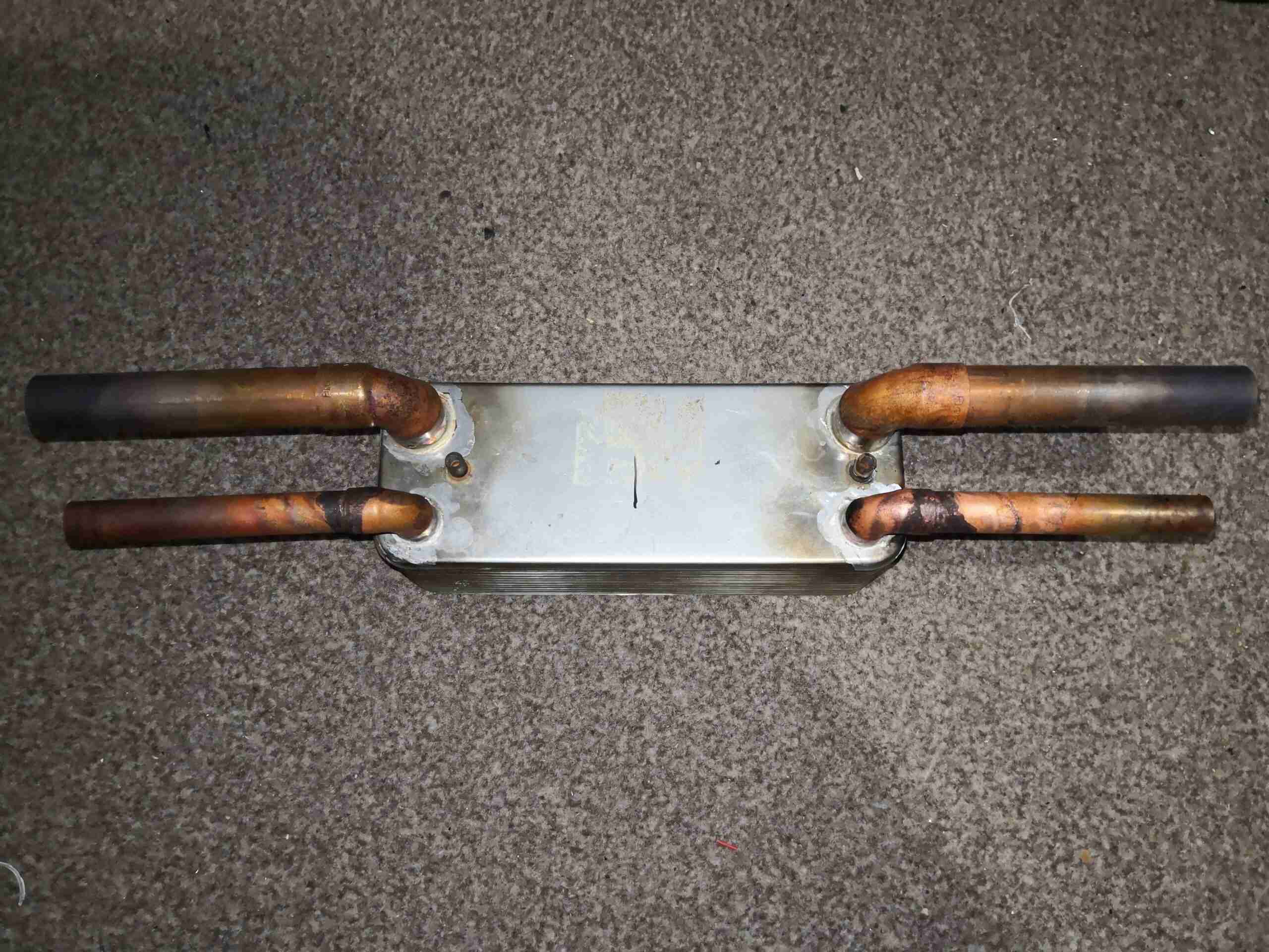
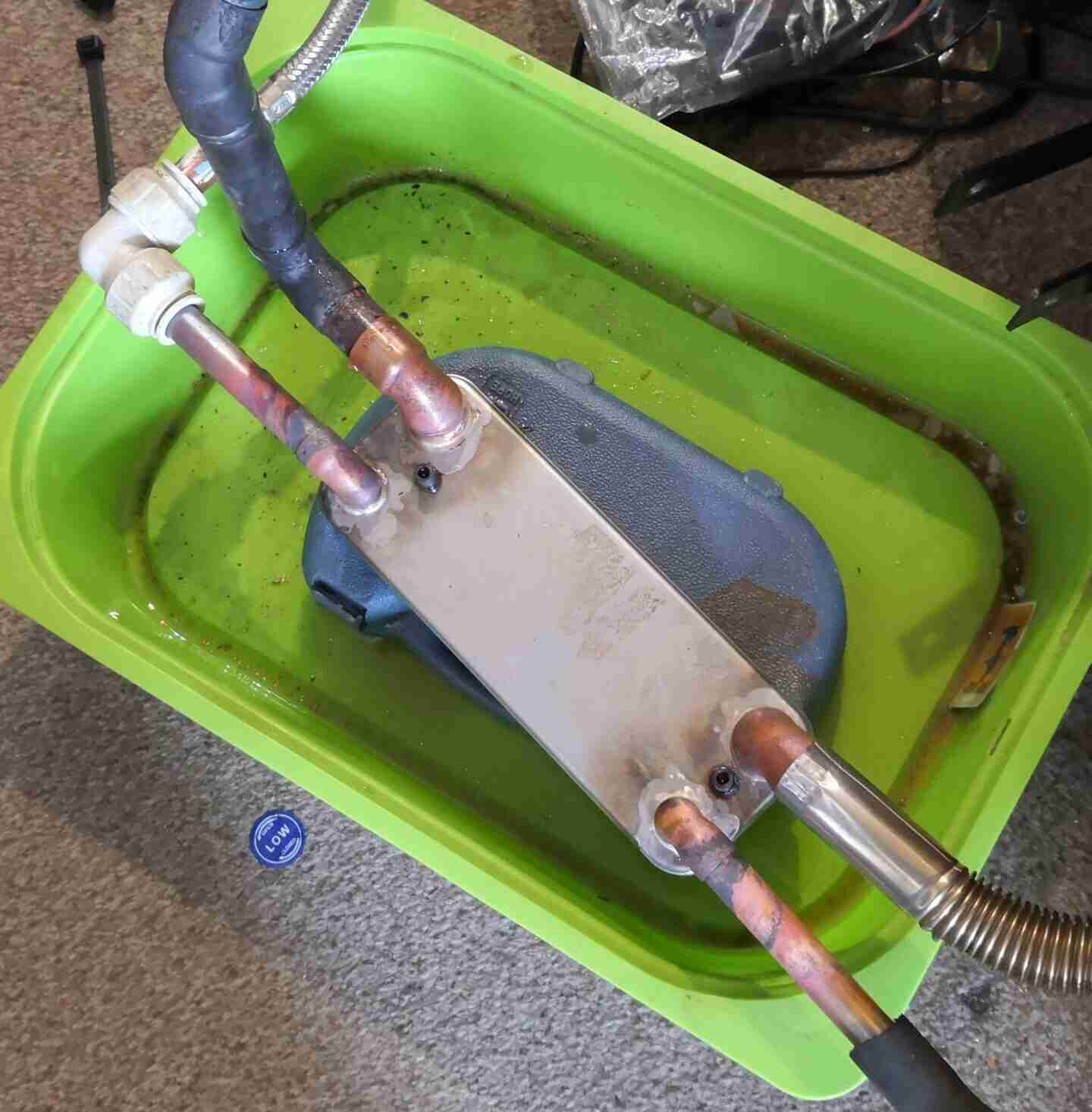
Heat Exchanger
Some time ago, I stripped an old gas combi boiler, and recovered some parts – most important here the HDW plate heat exchanger. This large chunk of stainless steel is a stack of formed plates, brazed together, that usually would heat Domestic Hot Water. In this instance it’s being repurposed to transfer heat from exhaust gas to water.
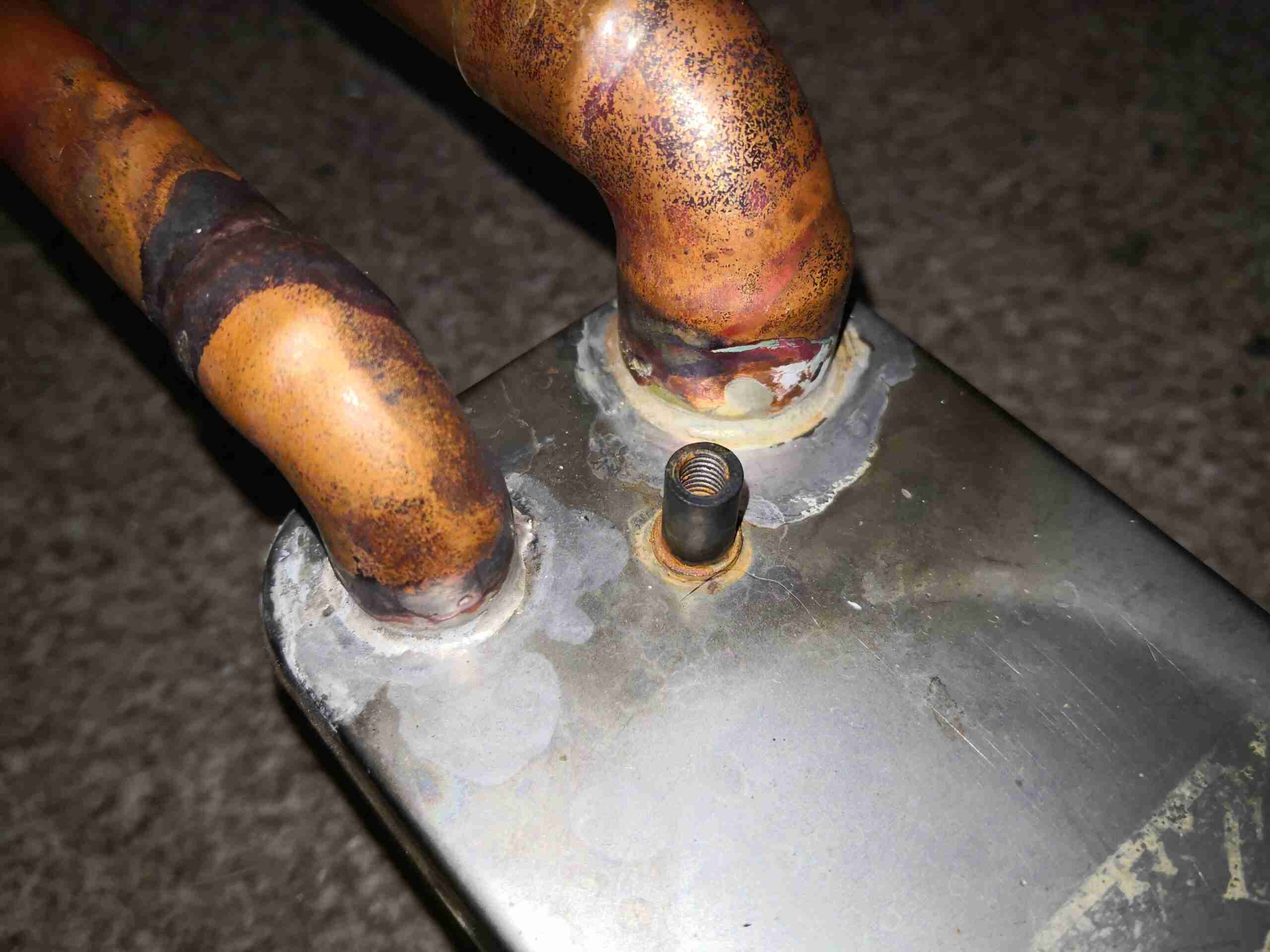
Brazed Connections
These heat exchangers are mounted in the boiler via a plate with O-Ring seals on, so they don’t really have fittings – just holes in the end plate. Solving this problem was simple – braze on some copper fittings with 55% silver brazing rod. The 22mm is the exhaust side, while the 15mm is the water side.
First Test
Cobbling together some random hose & fittings, along with a small water pump allowed me to run a first test. At this point there is no lagging at all on the exhaust system from the heater, so it’s going to shed a lot of exhaust heat into the air before it even gets to the heat exchanger. However I was able to get around 600W of heat into 15L of water, heating it up nicely. The heat exchanger is plumbed contra-flow here – exhaust comes in via the stainless tube on the bottom right, and water comes in through the speedfit elbow on the top left.
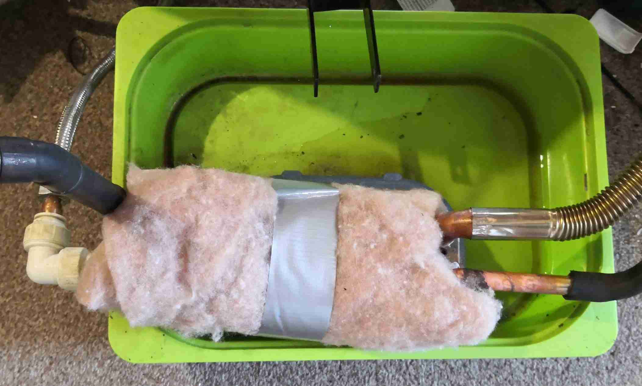
Lagged Heat Exchanger
After the temperature of the water tank hit a plateau at around 45°C, I decided to insulate everything the best I could with what I currently have. I’ve wrapped the heat exchanger with some recycled PET insulation here, just to hold the heat inside. I’m not concerned about the exhaust outlet being in contact with the fluff – this system is so effective at pulling the heat out of the exhaust that the gas exiting the far end is totally cold!
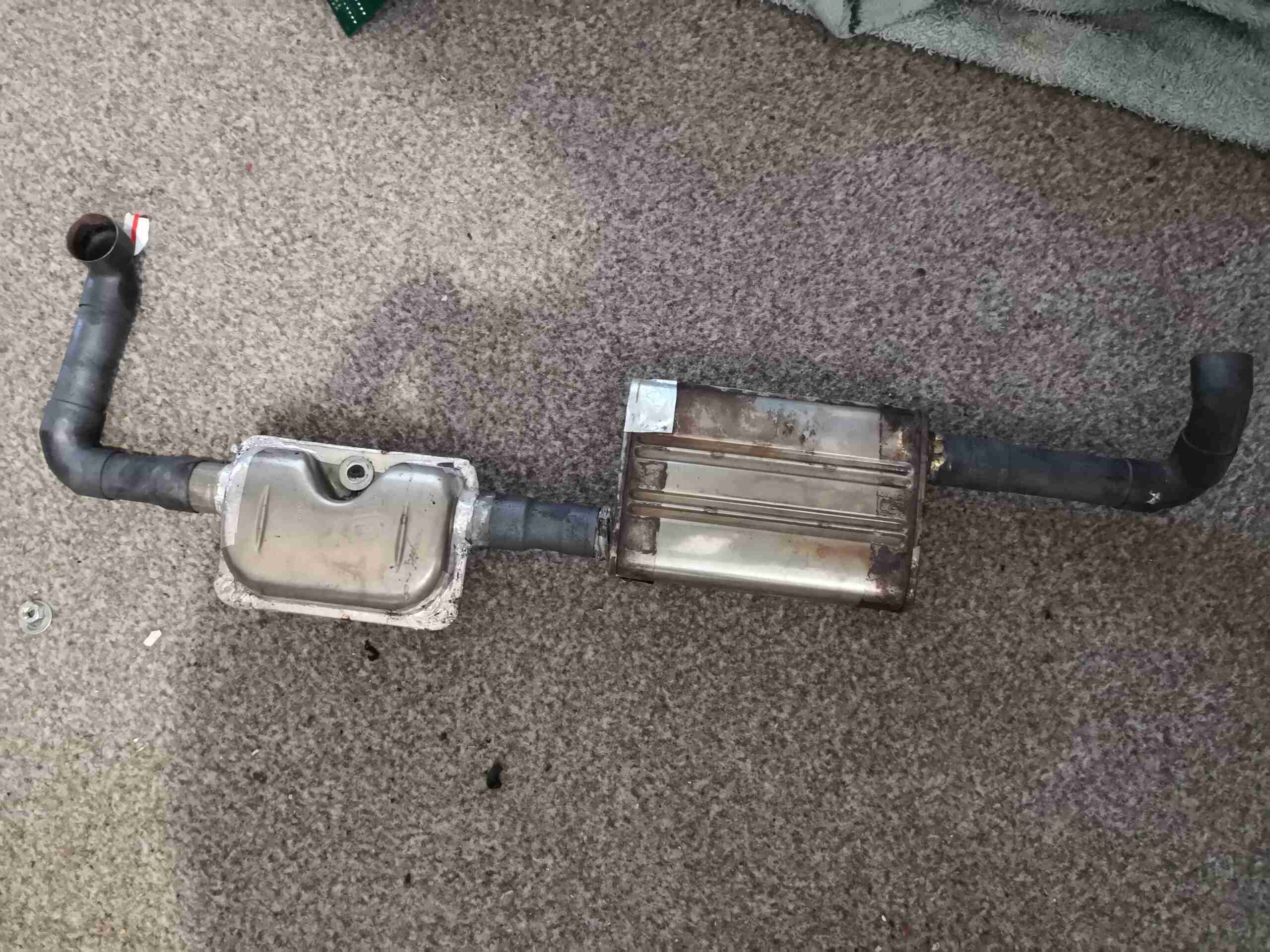
Unlagged Exhaust
Now it was time to get the exhaust system under the trolley insulated. This is the system removed from the unit entirely. This is constructed from copper pipe, brazed onto standard silencers. Deadening the sound from the unit is important, as this gets used on campsites!
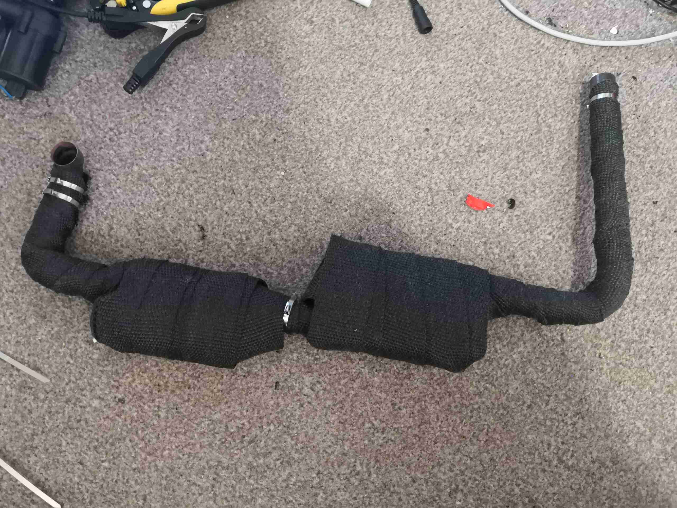
Fibreglass Tape Insulation
An hour & some itchiness later, the exhaust is completely covered in fibreglass insulation, secured in place with stainless steel ties.
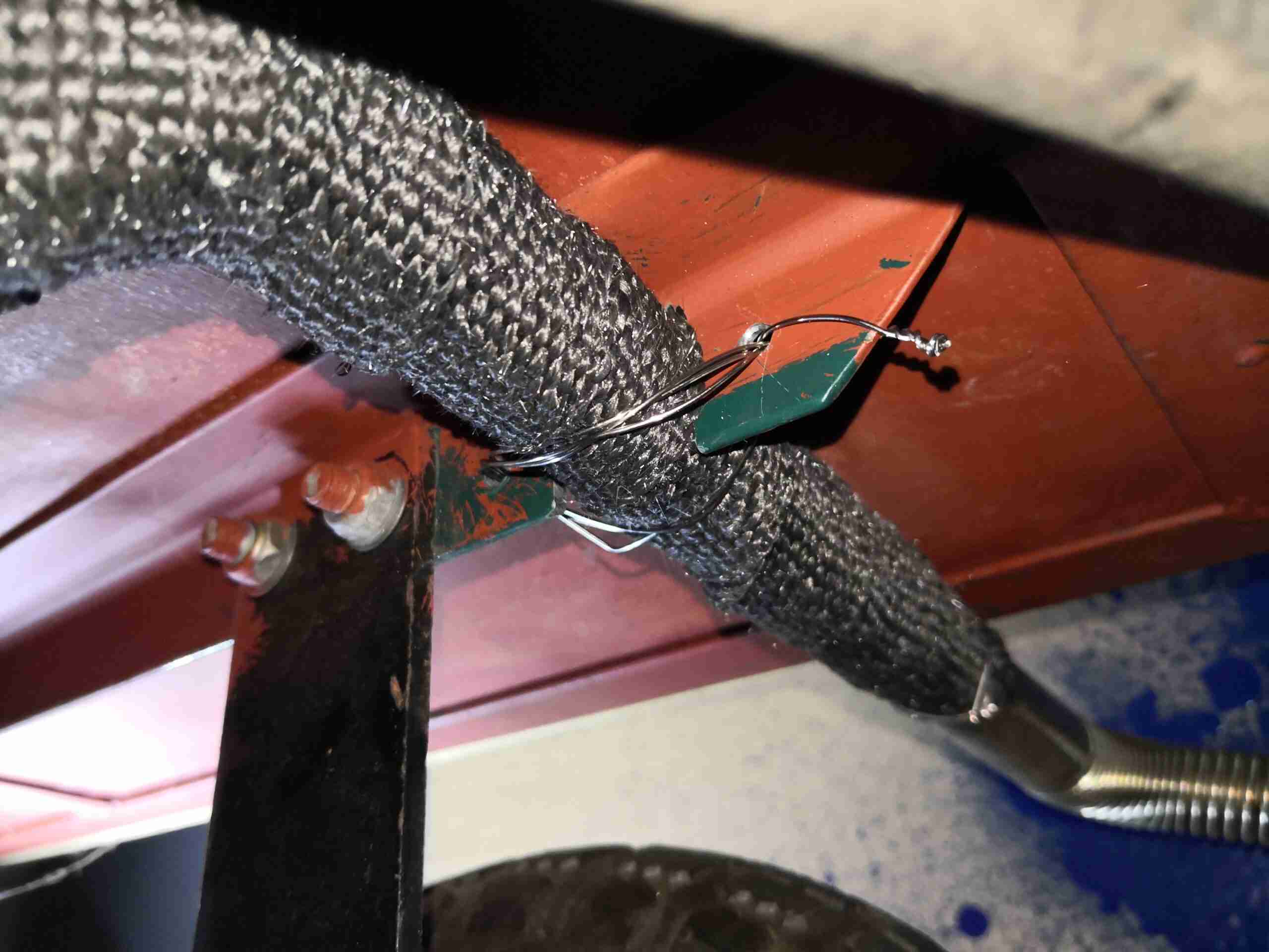
Exhaust Hanger
The exhaust originally passed through a close-fitting hole in the frame rail which would obviously not work now due to the thickness of the insulation layer, so this was modified with a grinder. Since there was now no support for this end of the exhaust, a pair of drilled holes & some stainless steel wire form a nice hanger!
With all this insulation in place (including around the tank & pump), the rig is now able to easily hit 65°C within a short time, so there has definitely been an improvement. At this point, it’s clear that waste heat recovery is worthwhile, so I’ll be building a proper rig to capture this energy for reuse!
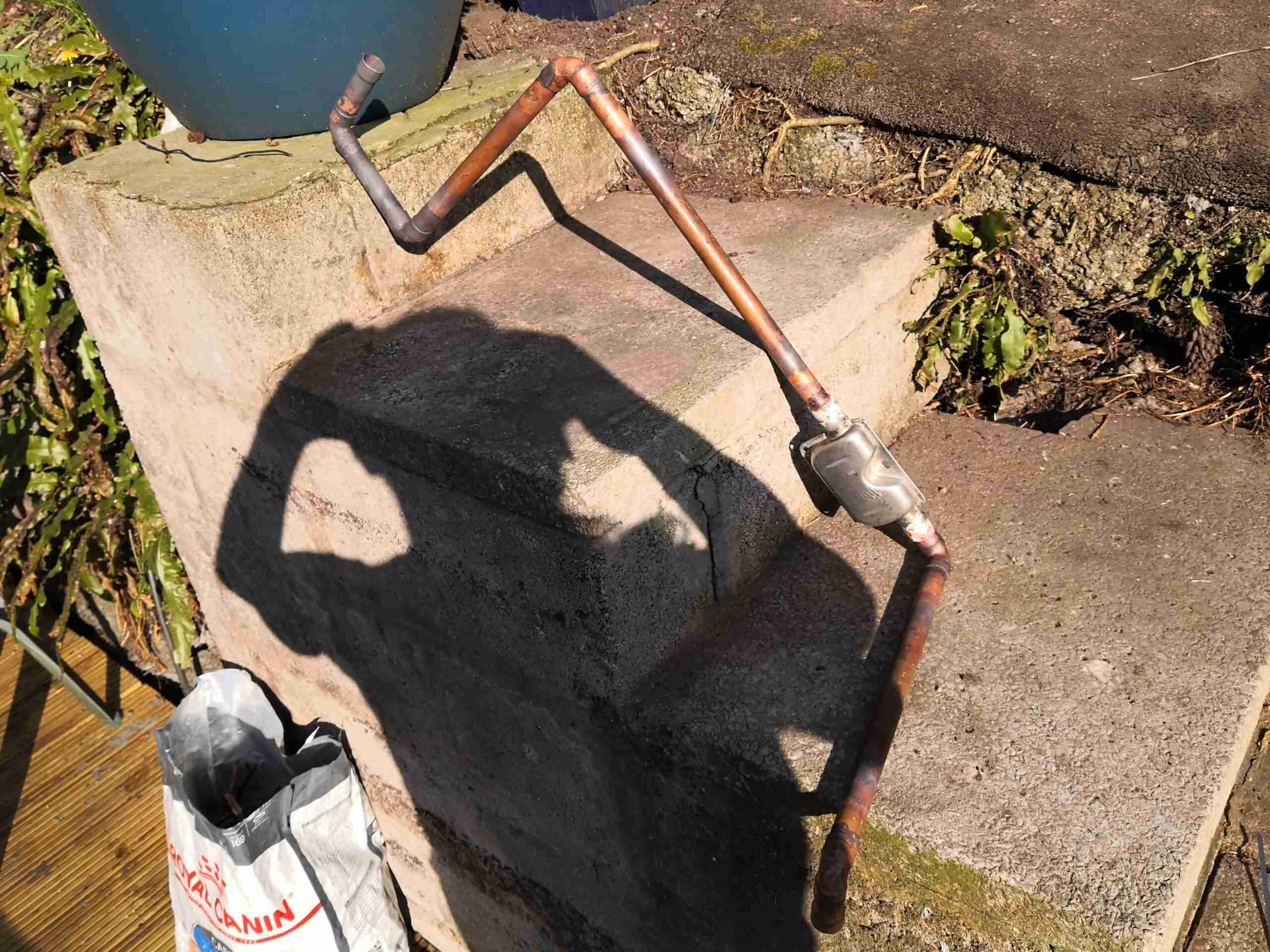
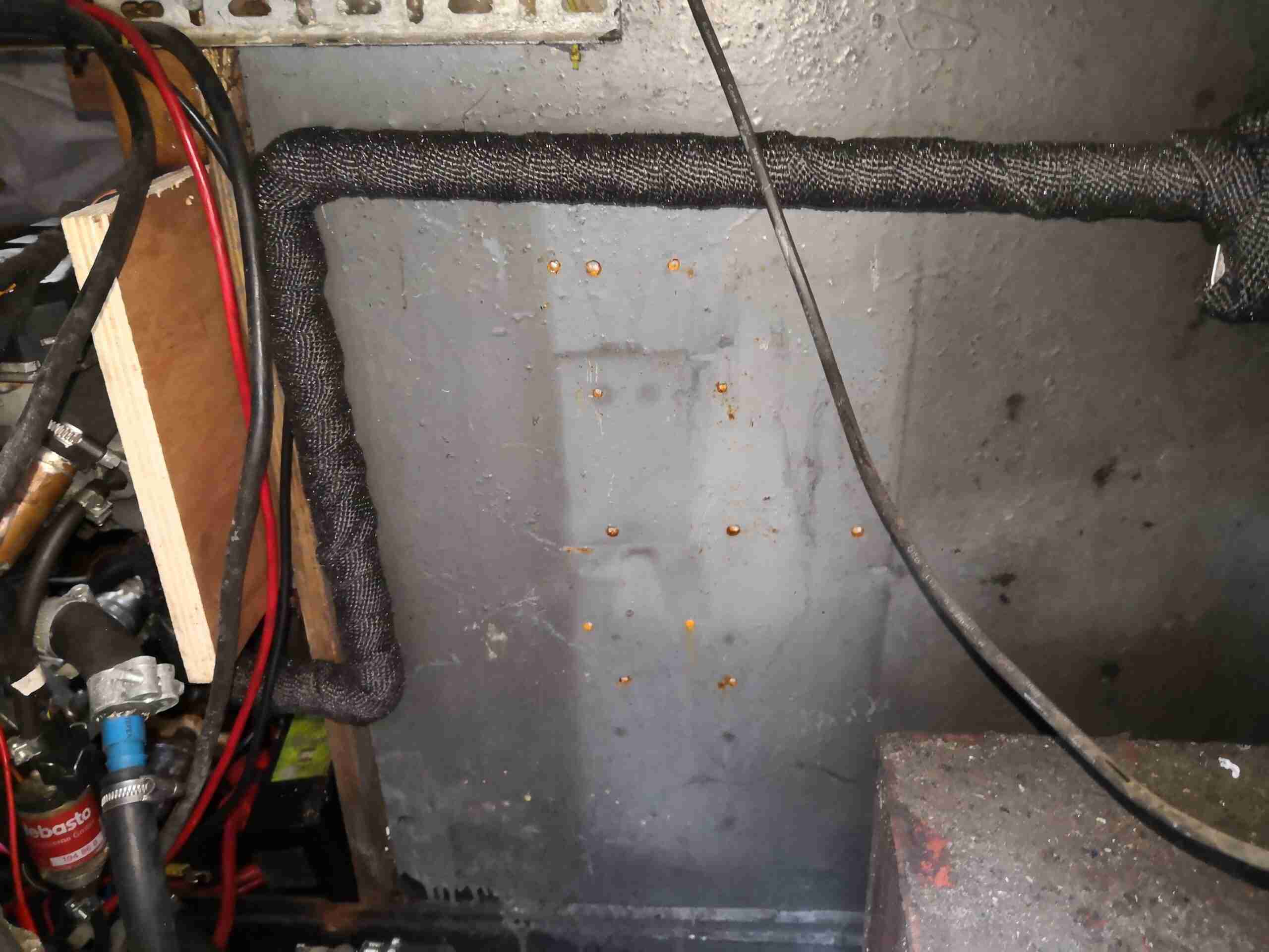
Since rebuilding the burner for the Webasto water heater on board nb Tanya Louise, I figured it was about time I sorted the exhaust out as well. The standard Eberspacher / Webasto type exhaust system components are shit. Nothing is properly gas tight, no matter how you build the system, due to how the pipe is constructed – it’s spiral ribbed stainless flexi tube, and even proper clamps don’t exert enough force to create a gas seal on the fittings, leaving gaps in the spiral for exhaust to leak out. Unfortunately I don’t have a photo of the old exhaust setup – it was however awful.
So to fix the problem of the messy setup, and to fix the issue of leaking exhaust gases, I got to work creating a custom system from 22mm copper pipe, brazing all the joints together.
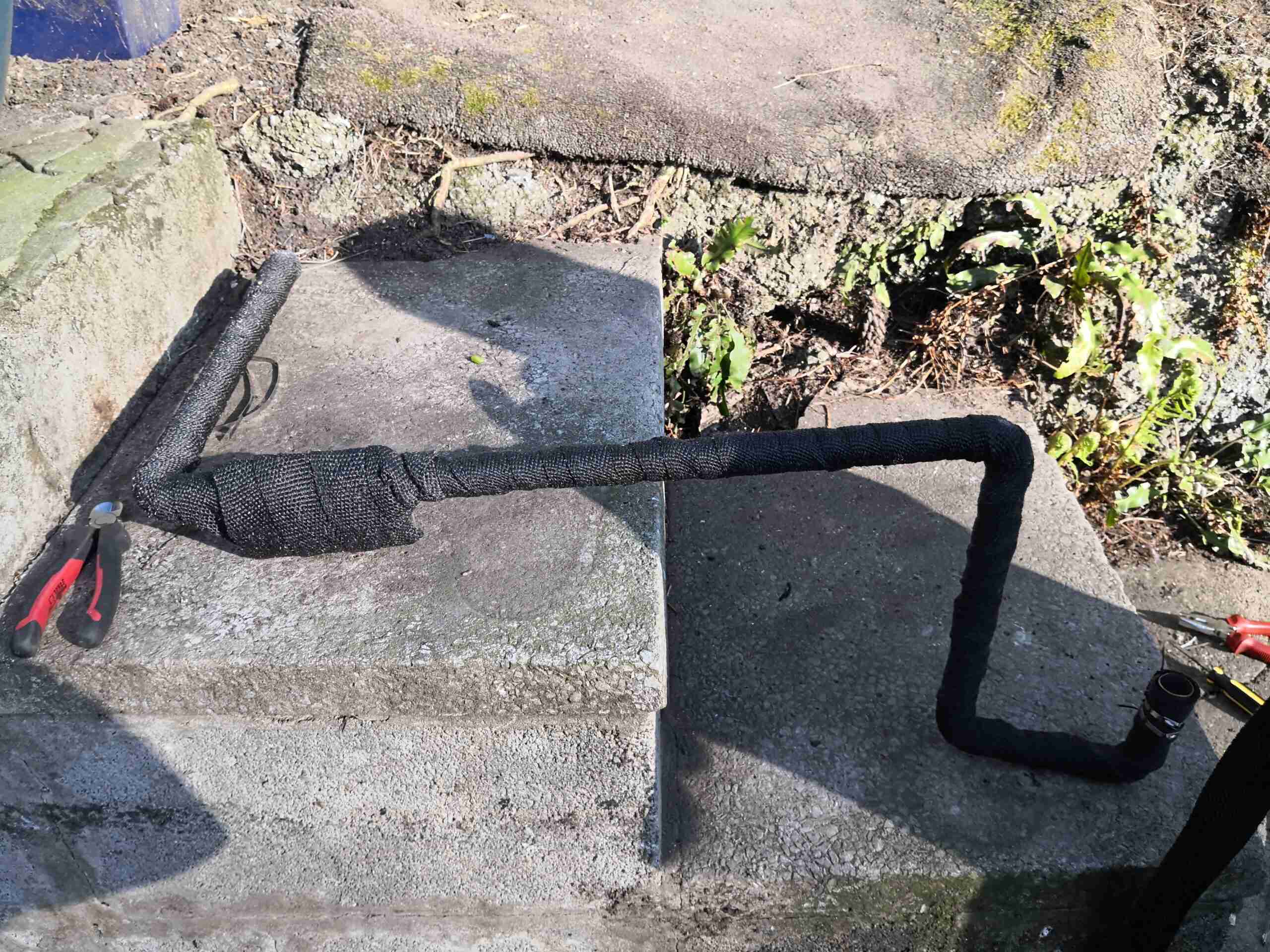
Completed Exhaust
Here’s the completed system, matched to the location of the heater unit in the engine bay, and the exhaust skin fitting. The ends of the pipe are expanded with a hydraulic tool to allow them to fit onto the heater & skin fitting, these being too large for 22mm pipe normally.
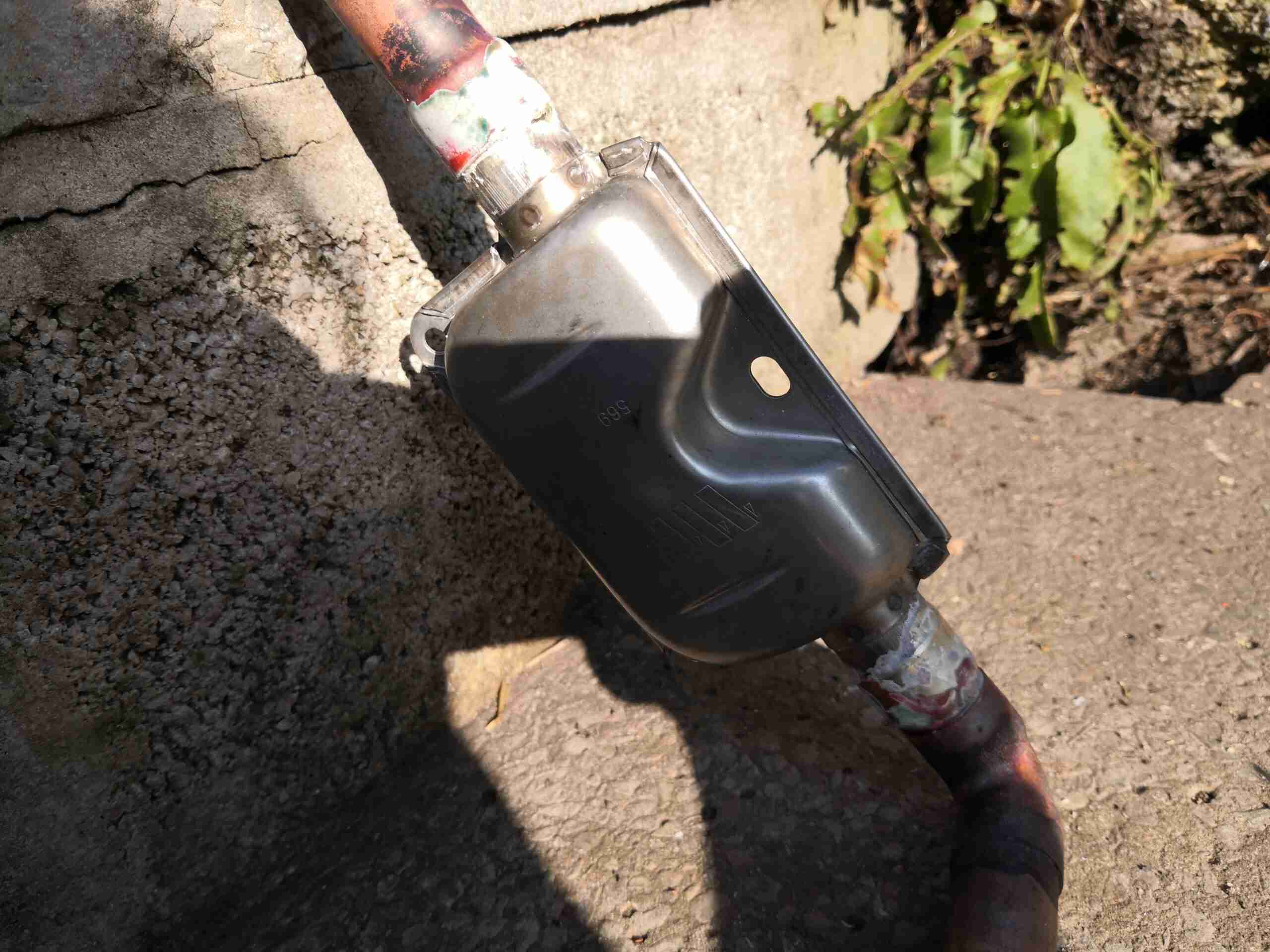
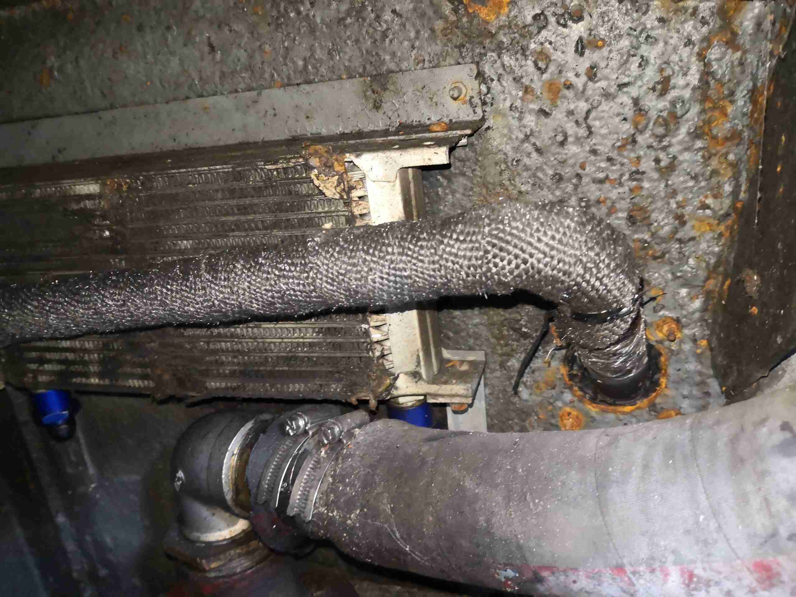
Brazed Muffler
The muffler is also fully brazed to keep exhaust gases inside the exhaust. These are supplied just crimped together as they’re intended for use under vehicles. A sealed marine grade exhaust silencer is available, but very expensive. Again the copper pipe ends are expanded with the hydraulic tool to allow them to fit into place on the stainless tails. Brazing was done with 55% silver brazing rod.
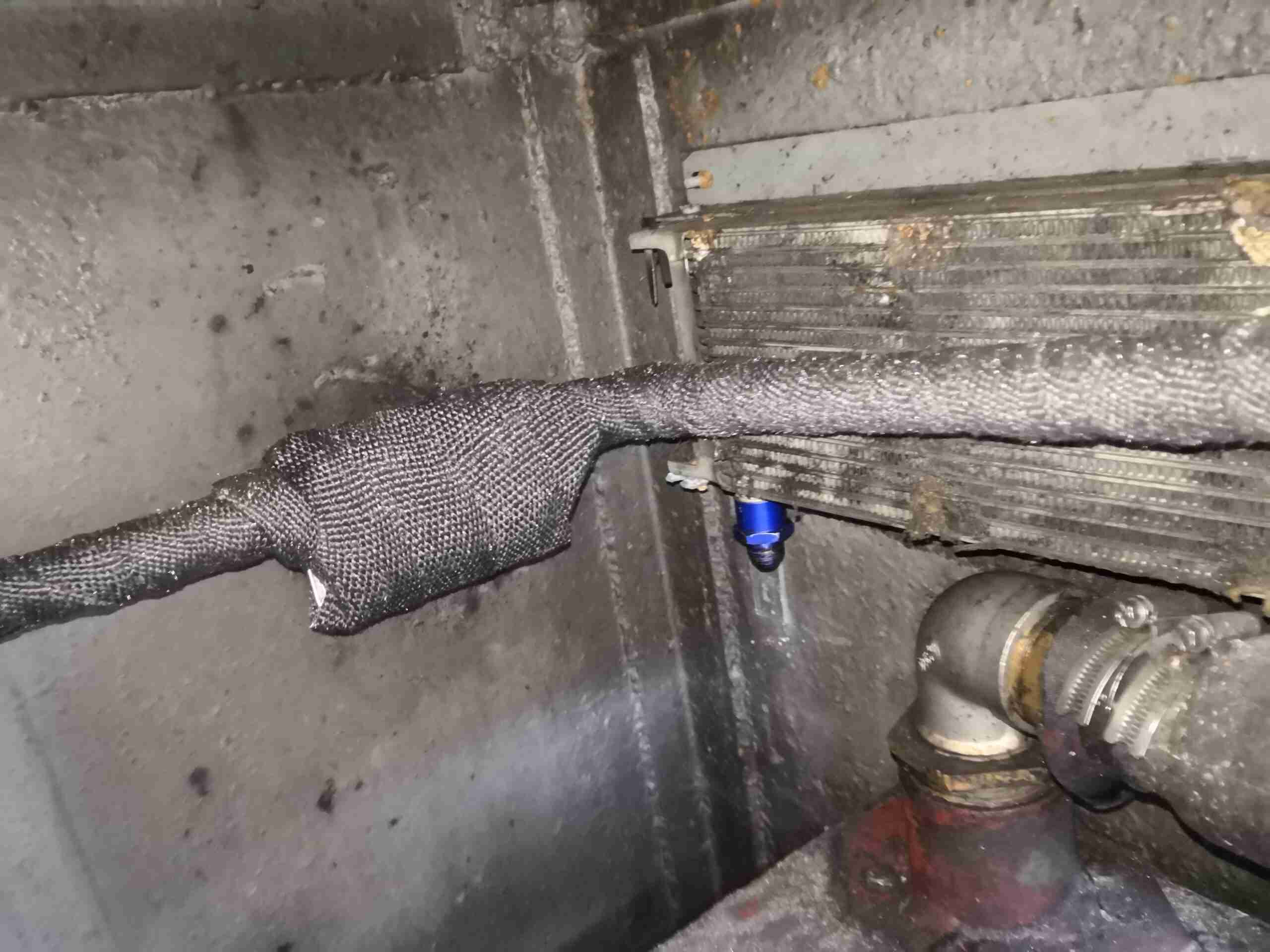
Fibreglass Wrap
To keep the heat away from sensitive parts in the engine bay, the entire assembly has been wrapped in fibreglass insulation tape, and secured with stainless steel ties. It’s important to use only stainless in these applications – the fibreglass wrap will hold any moisture in contact with all the parts, and mild steel will rapidly convert back into Iron Oxide 😉
Heater End
The heater itself is on the other side of the plywood board in the photo, the cooling water pipework can be seen on the lower left, along with the diesel dosing pump. The main fuel tank is just visible in the bottom right corner.
Skin Fitting Connection
The other end is sized for a snug fit onto the exhaust skin fitting, just astern of the old oil cooler. This is set to be removed at some stage, and be replaced with an engine bay blower for ventilation.
Silencer
In the corner, next to the bulkhead sits the silencer.
In all, this setup also made the heater quieter, probably due to the longer length of exhaust pipework, which is now about 1.5 metres from the heater outlet to the skin fitting. This is a bonus – the exhaust of these heaters without any silencing sounds like a jet engine!
Since the entire country is on Coronavirus lockdown at the moment, I figured it was time to get round to finishing off a couple of small blog posts while waiting for the restrictions to be lifted 😉
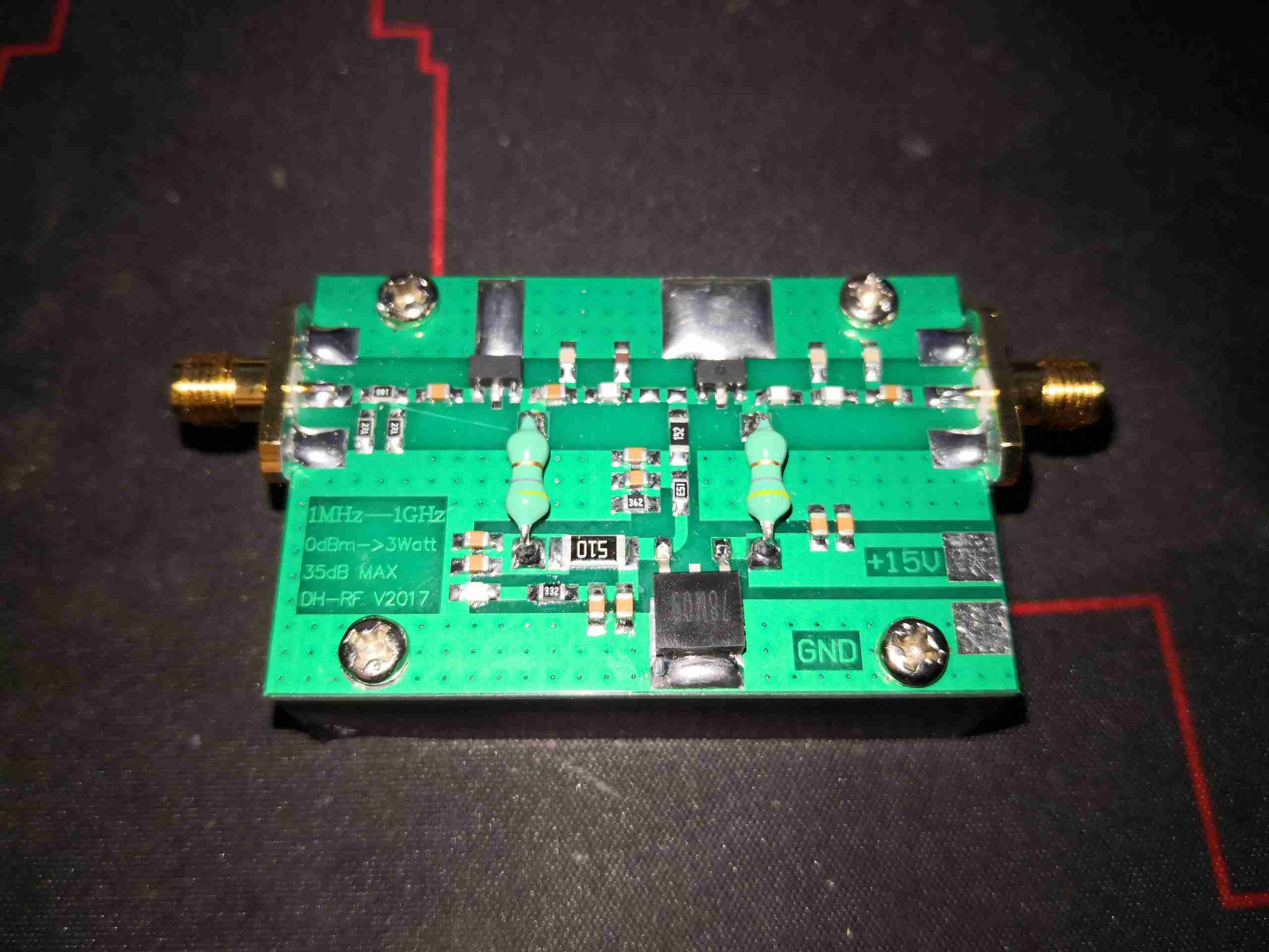
3W 1GHz Amplifier
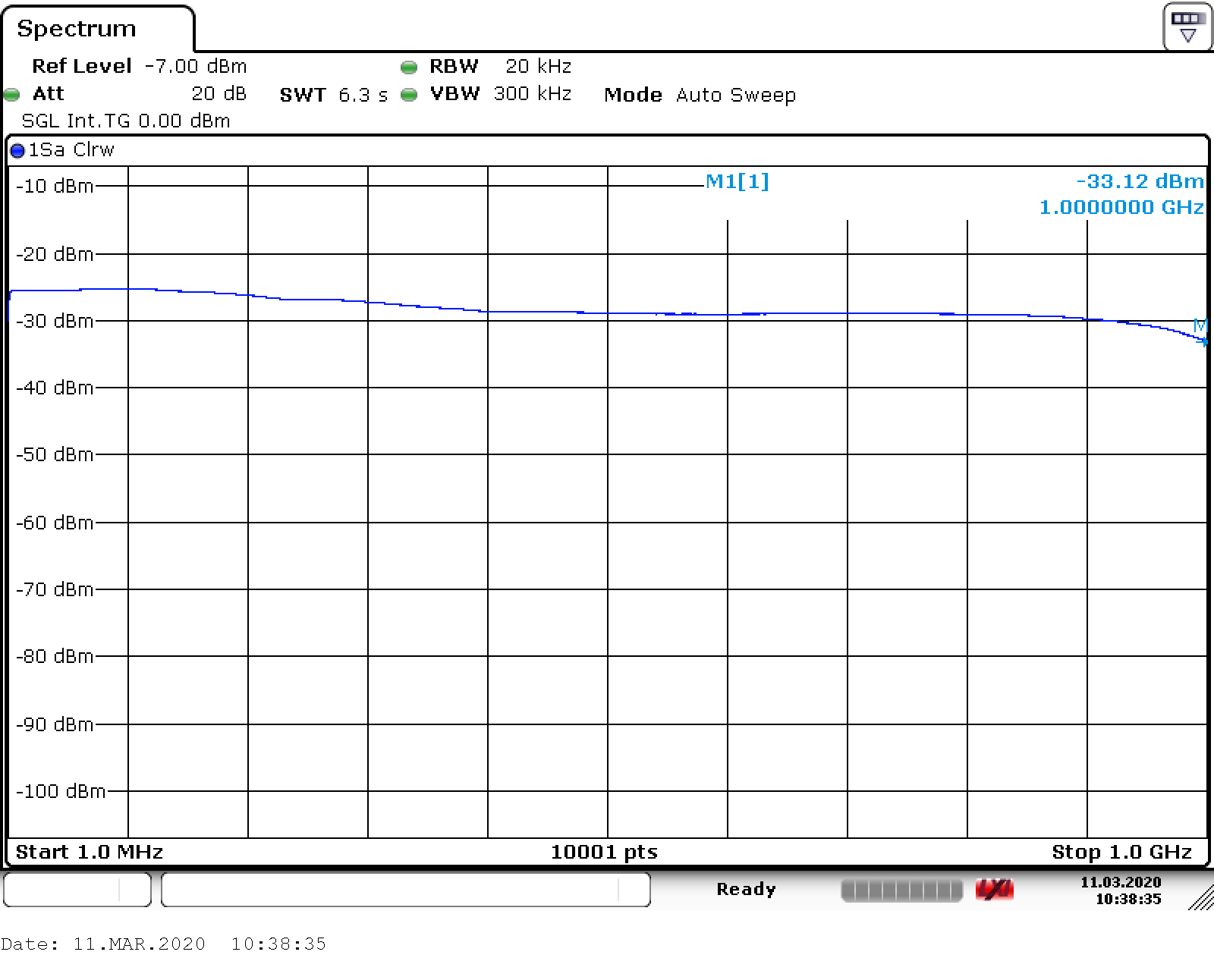
This is a small two-stage linear amplifier module available on eBay fairly cheap for SDR operation.This unit claims 3W (34.8dBm) power output at 0dBm input, however not surprisingly, this amplifier isn’t quite flat across the frequency range.
Frequency Response
Here’s the readout from an R&S FSV7 spectrum analyser. The amplifier is being driven from the analyser’s tracking generator at 0dBm, and the output is fed back into the input via 60dB of external power attenuation. The span here is 1MHz-1GHz, and at the top end the frequency response is already beginning to drop off a cliff – the 1GHz rating appears to be the 3dB down point. The rated output power of 3W appears to only be attainable below 100MHz for the rated 0dBm input, after that it drops pretty quickly to about -3dB.
Frequency
Output - dBm
Output - W
100MHz
34.74
2.97
144MHz
34.4
2.75
200MHz
33.81
2.40
315MHz
32.59
1.81
433MHz
31.46
1.39
500MHz
30.91
1.23
600MHz
30.87
1.22
700MHz
31.04
1.27
800MHz
30.95
1.24
900MHz
30.24
1.05
1000MHz
26.86
0.48
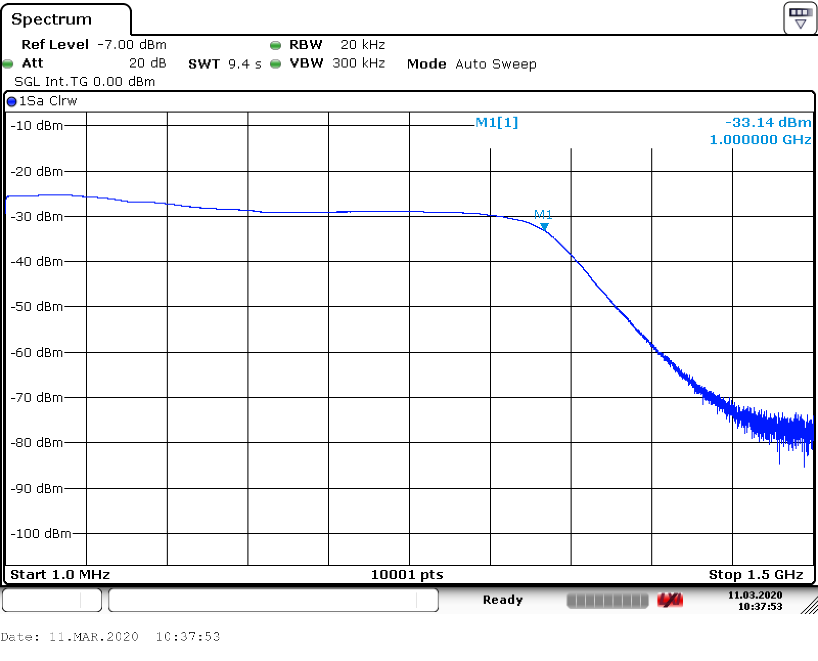
Extended Span
Extending the frequency span of the analyser shows the roll off at high frequency – this module really isn’t usable above the rated frequency range.
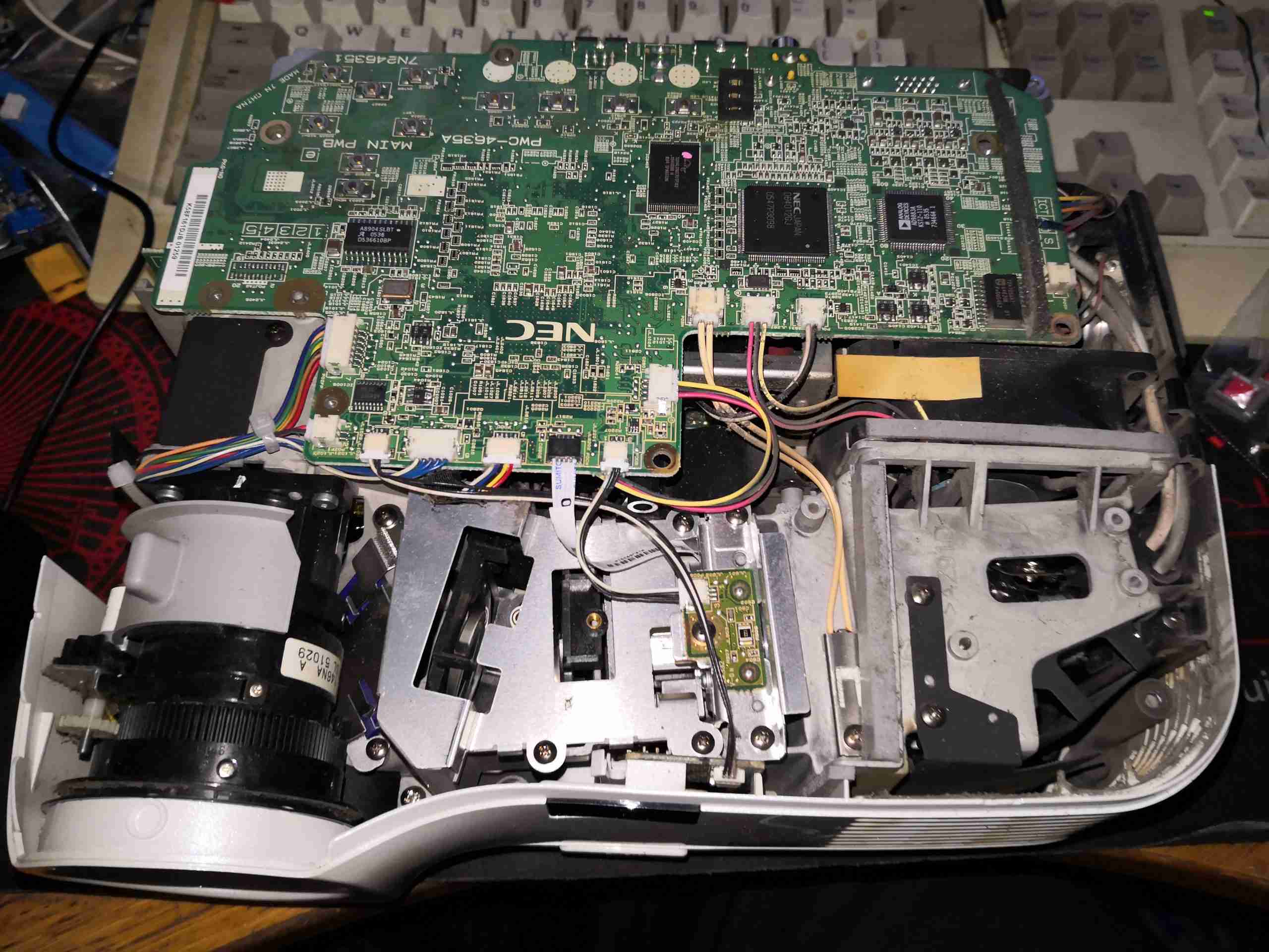
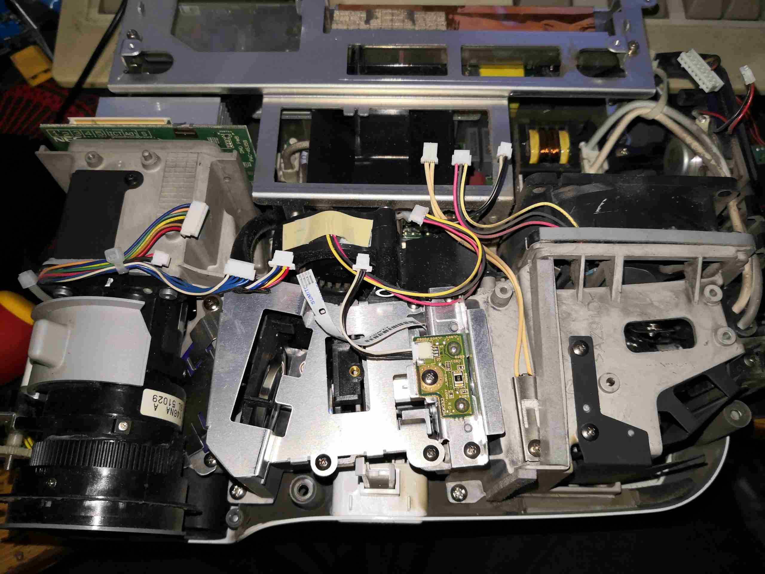
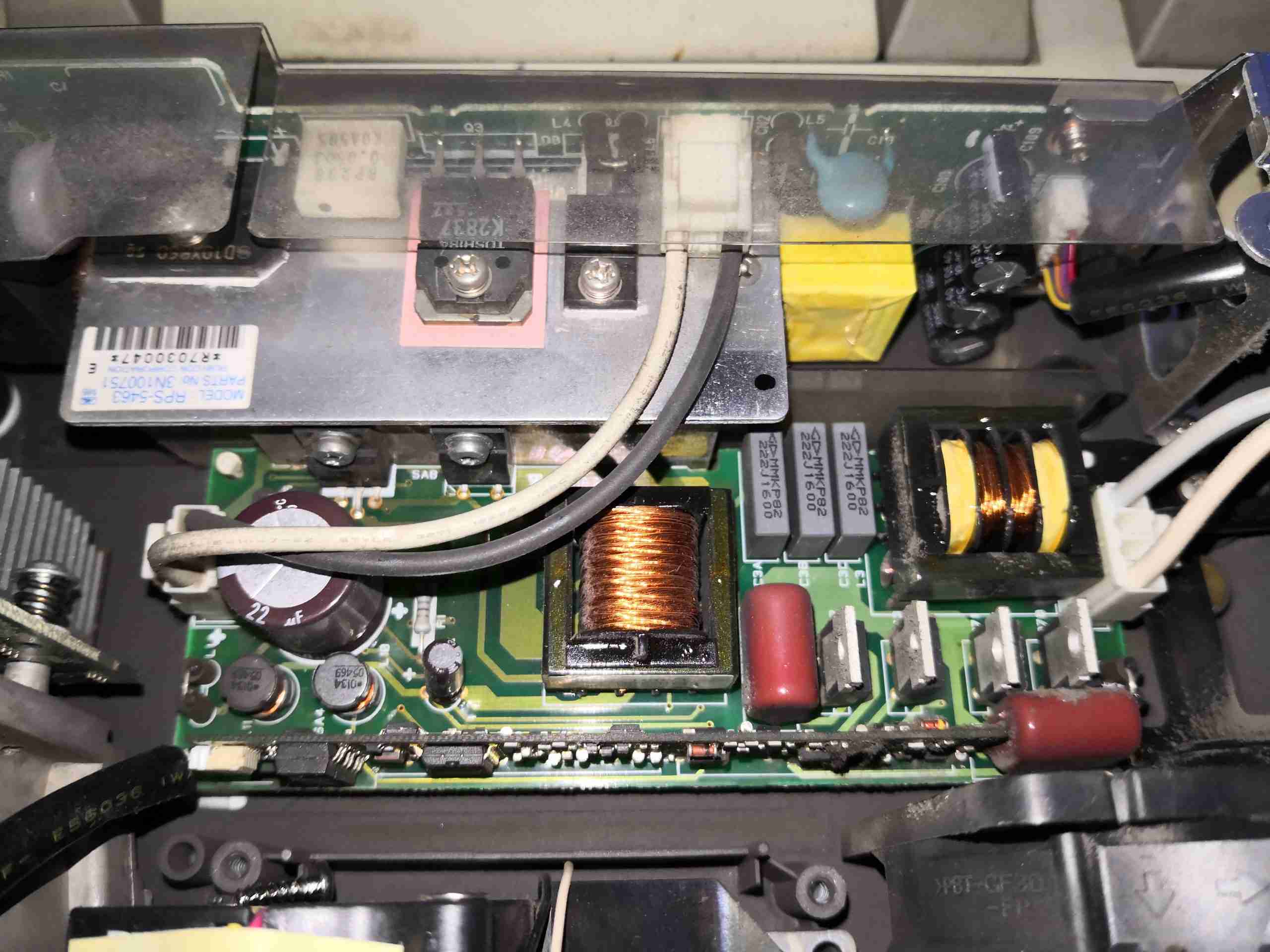
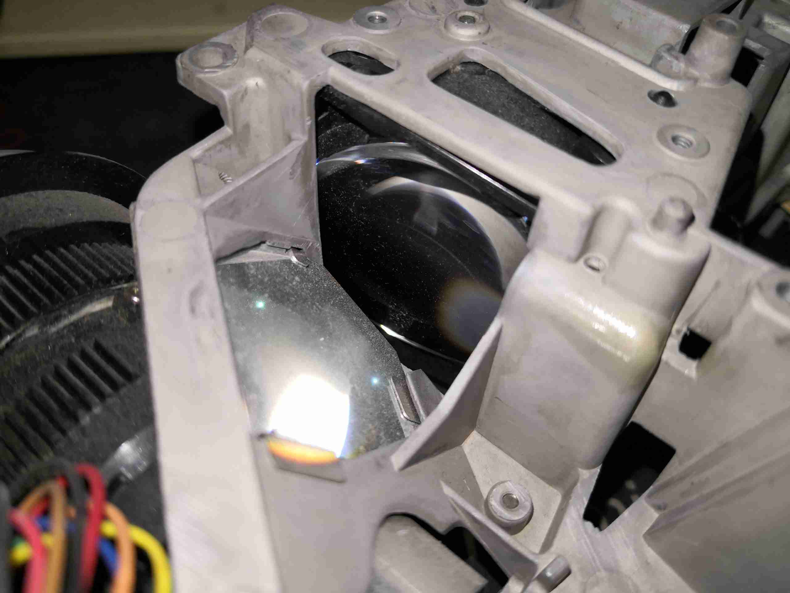
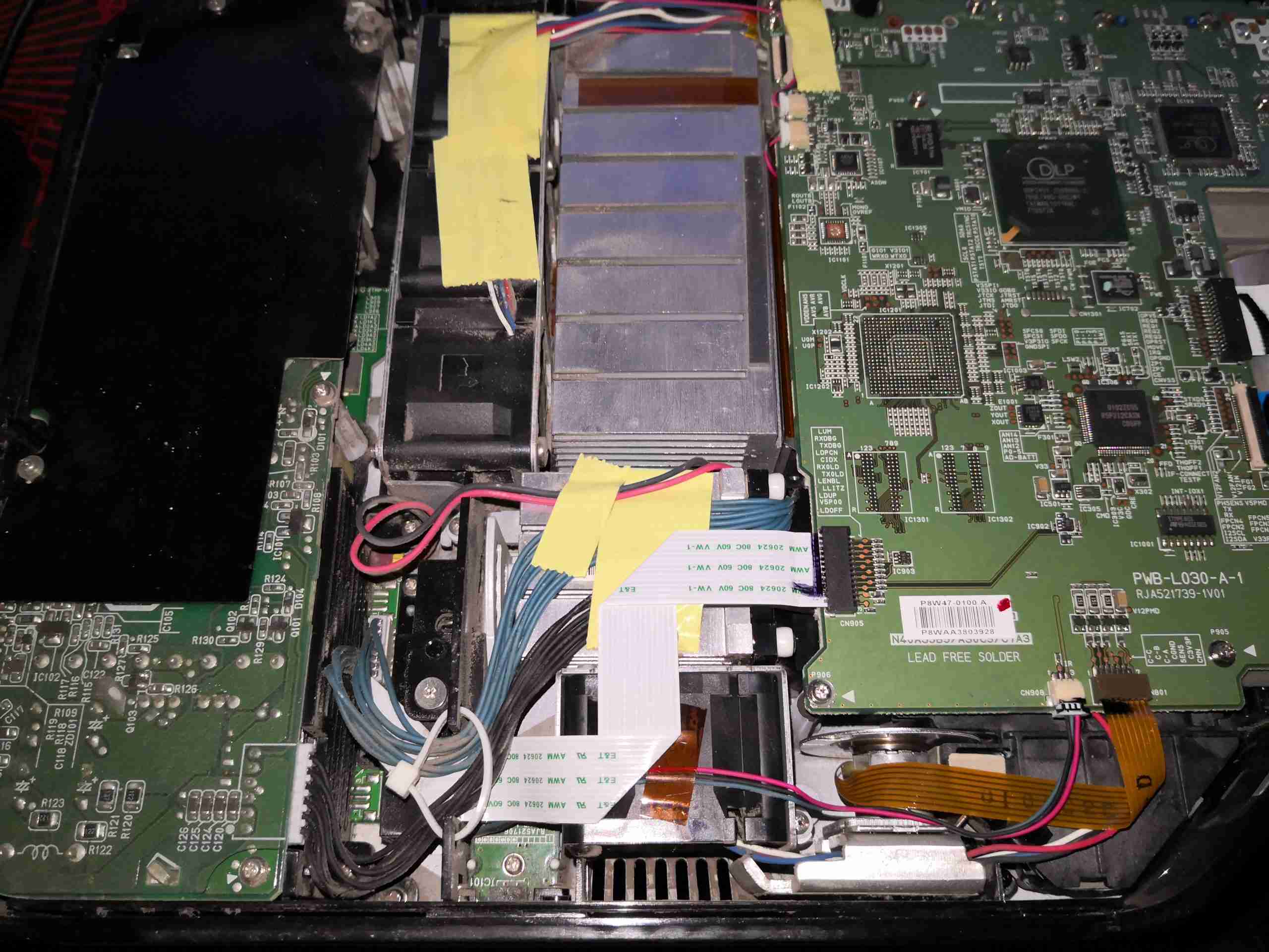
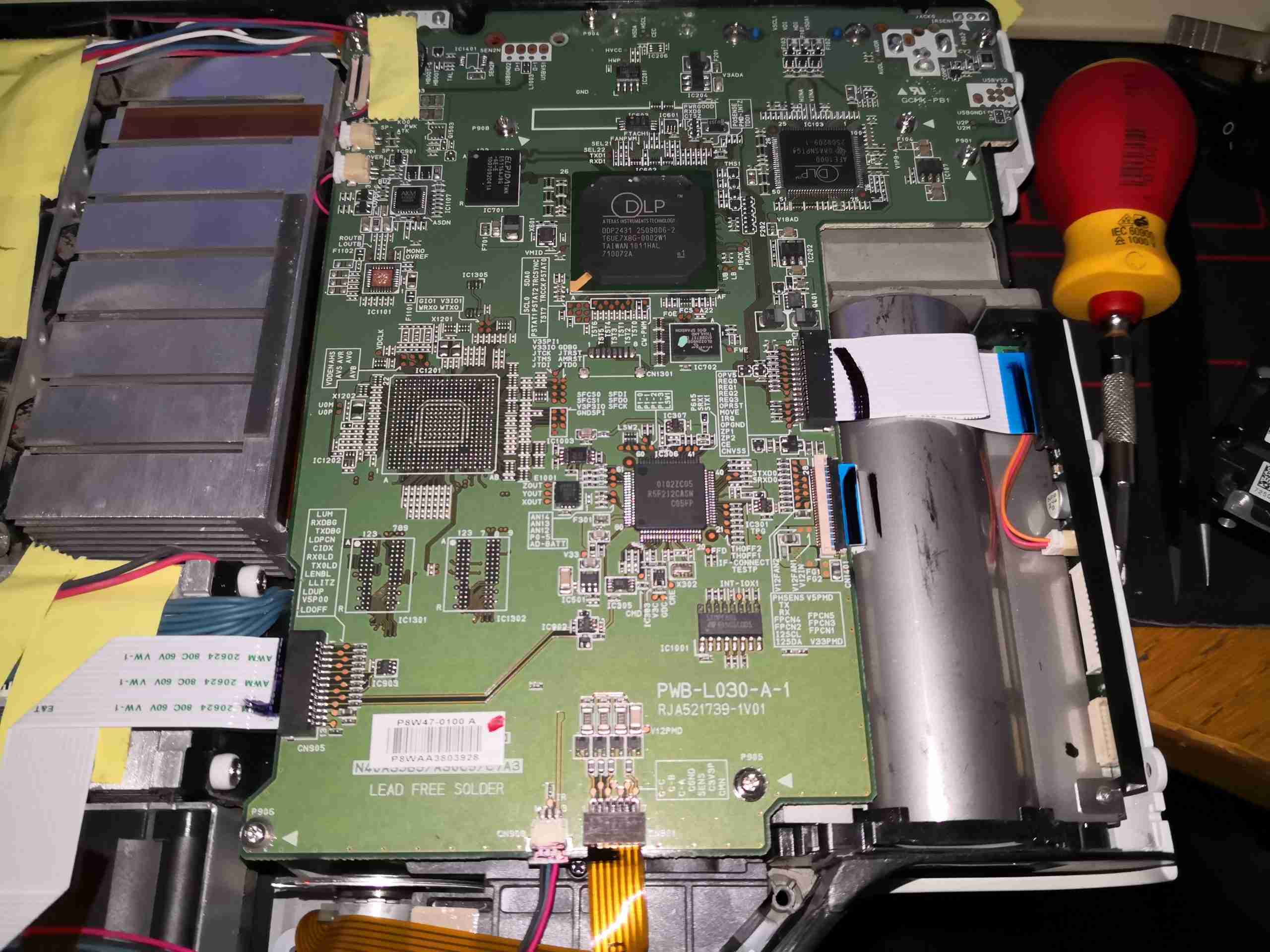
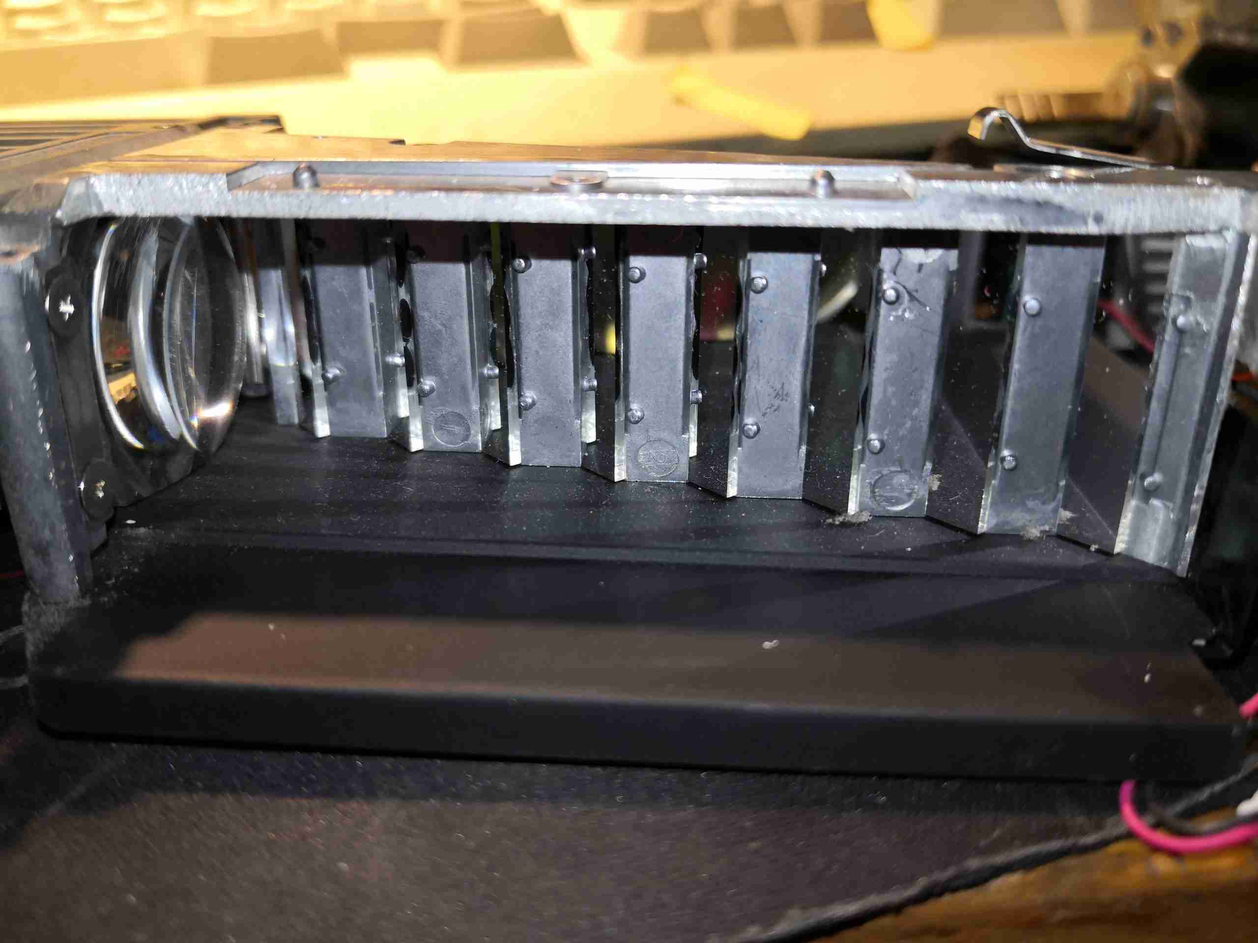
Time for another projector! This one was brought to me with a fault, described as a shadow in the middle of the image, shortly after the lamp was replaced after exploding. This is an older DLP projector, with a UHP mercury lamp. I’ve already removed the top cover of the projector here, showing the internals. The light engine is along the front of the unit, with the lamp on the right. The main control board on top contains all the image processing logic & control functions.
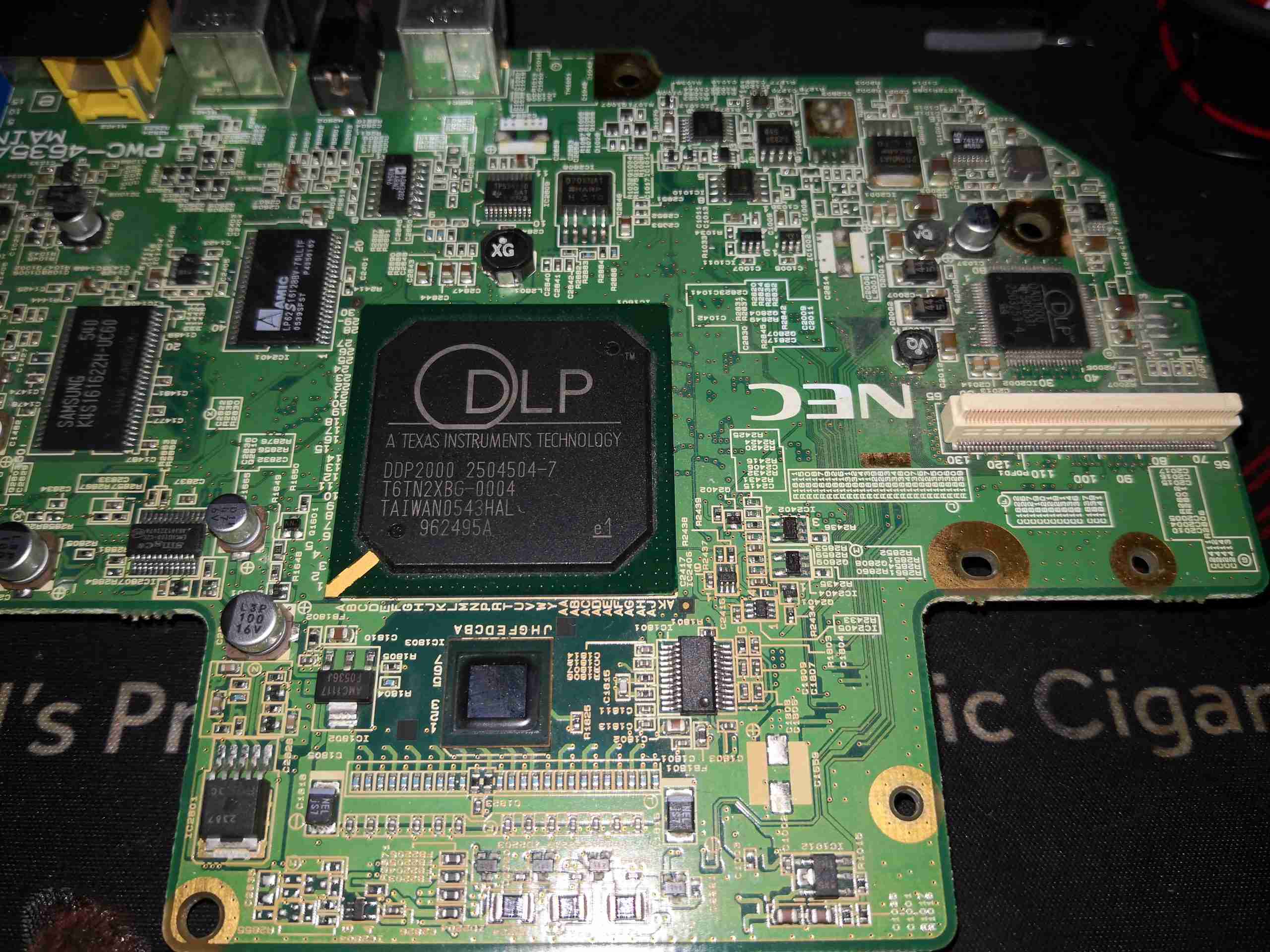
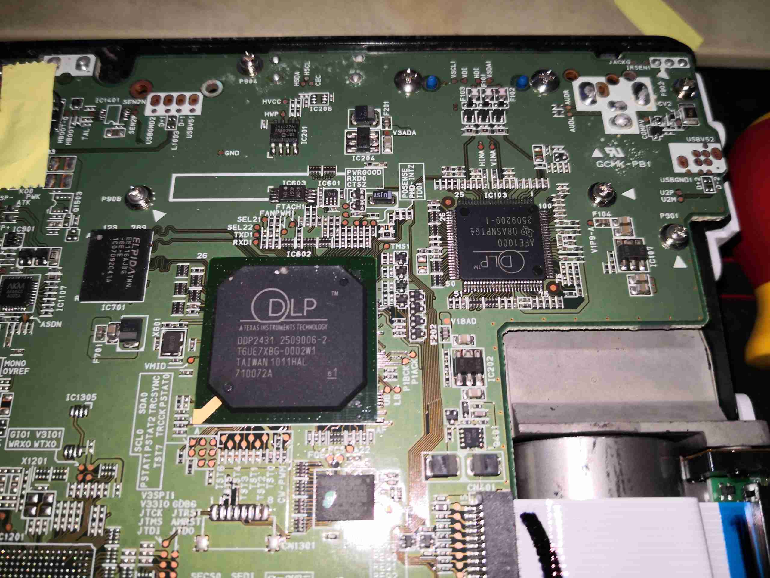
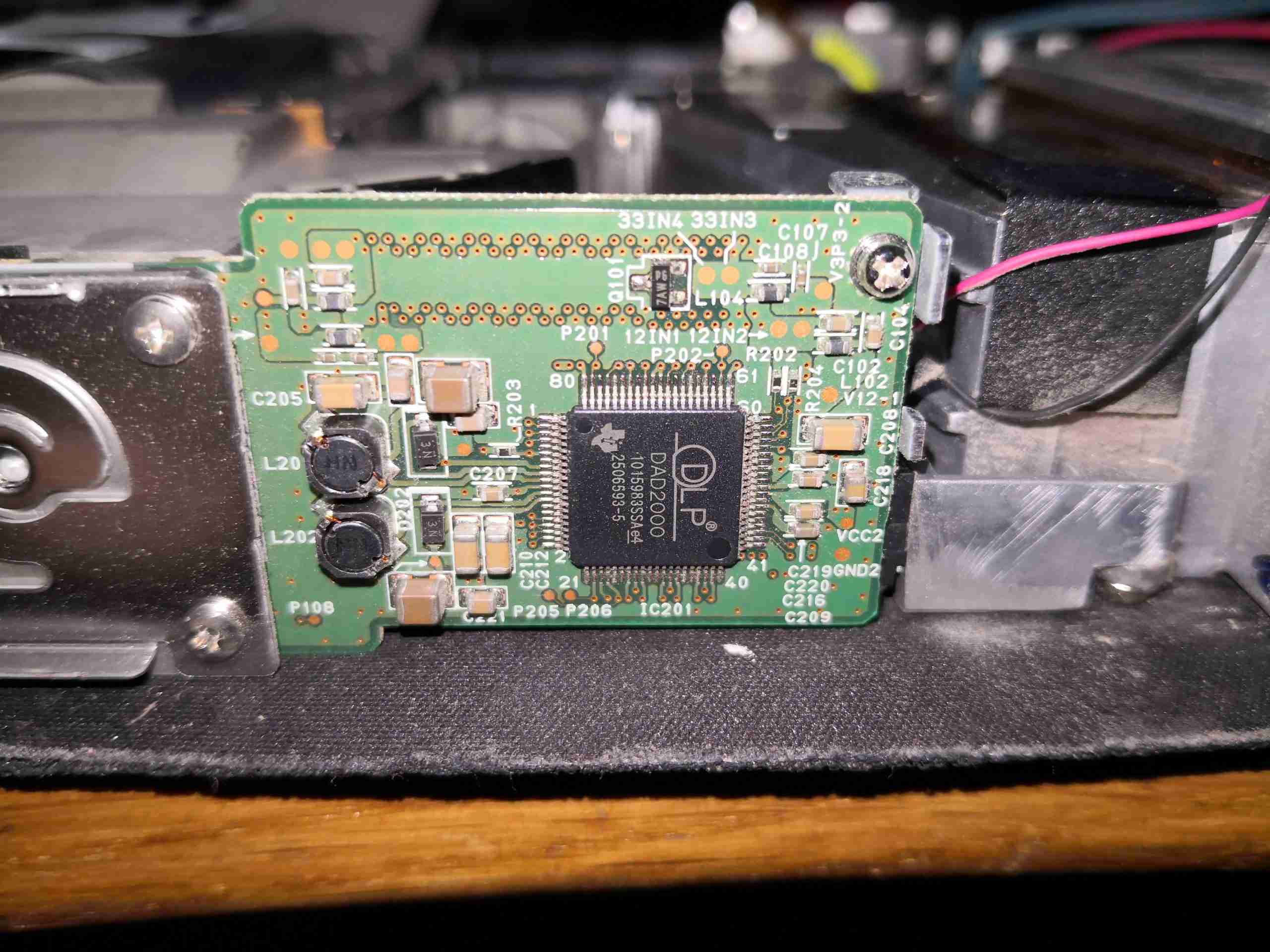
Mainboard
The other side of the mainboard holds the processing chipset. This is probably one of the biggest flip-chip BGA packages I’ve ever seen, the DDP2000. Along with the DAD1000 on the right, these format & send the image data to the DLP chip, via the large white header.
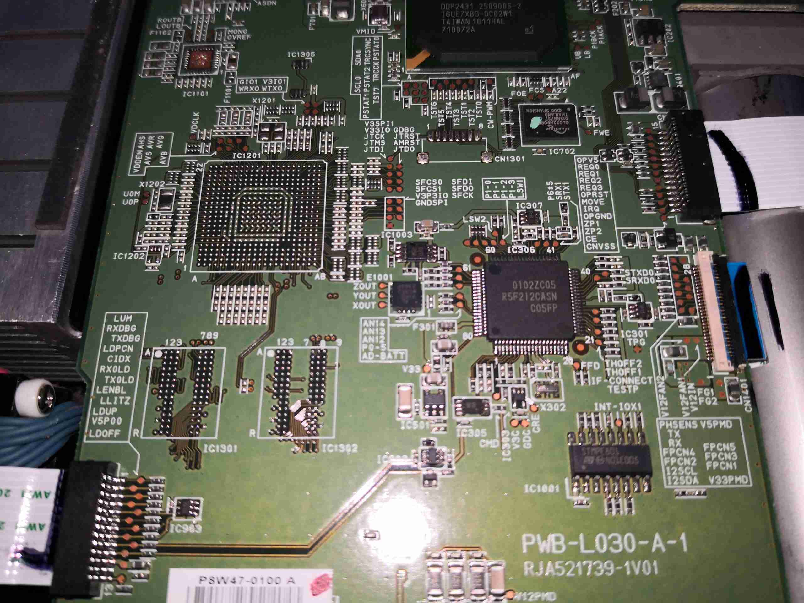
Main PCB Removed
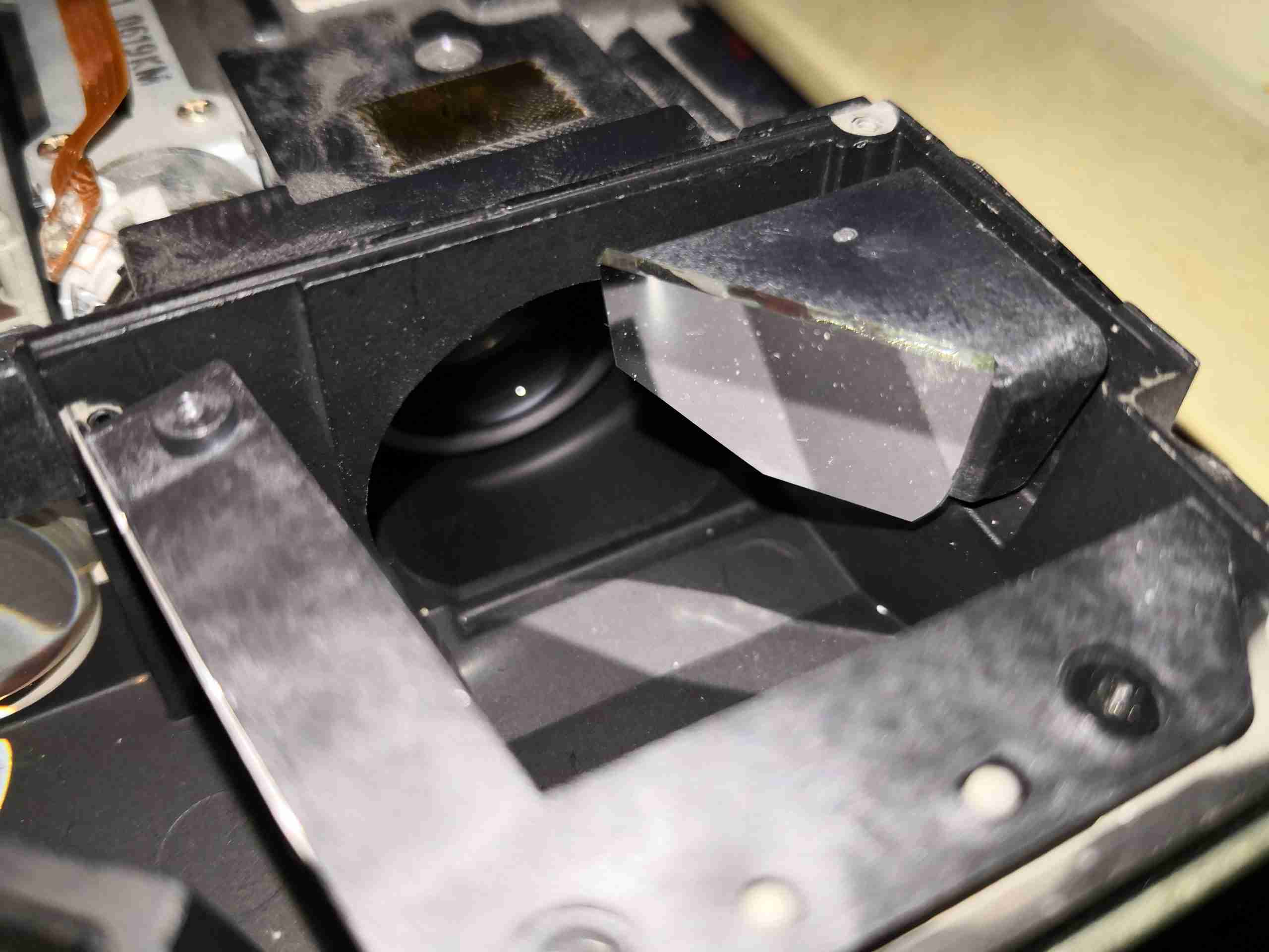
After the mains PCB is removed from the chassis, the rest of the light engine is visible. The DLP is hidden on the left, behind the large heatsink & interface PCB. The light engine is spread out a lot more on this projector, across the entire front of the unit.
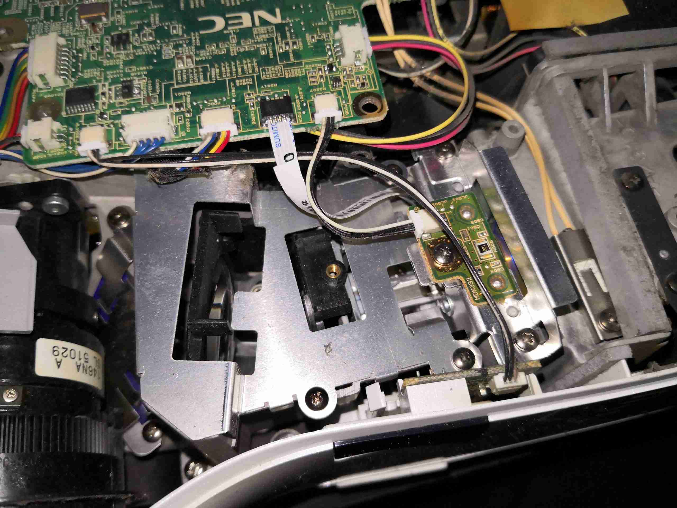
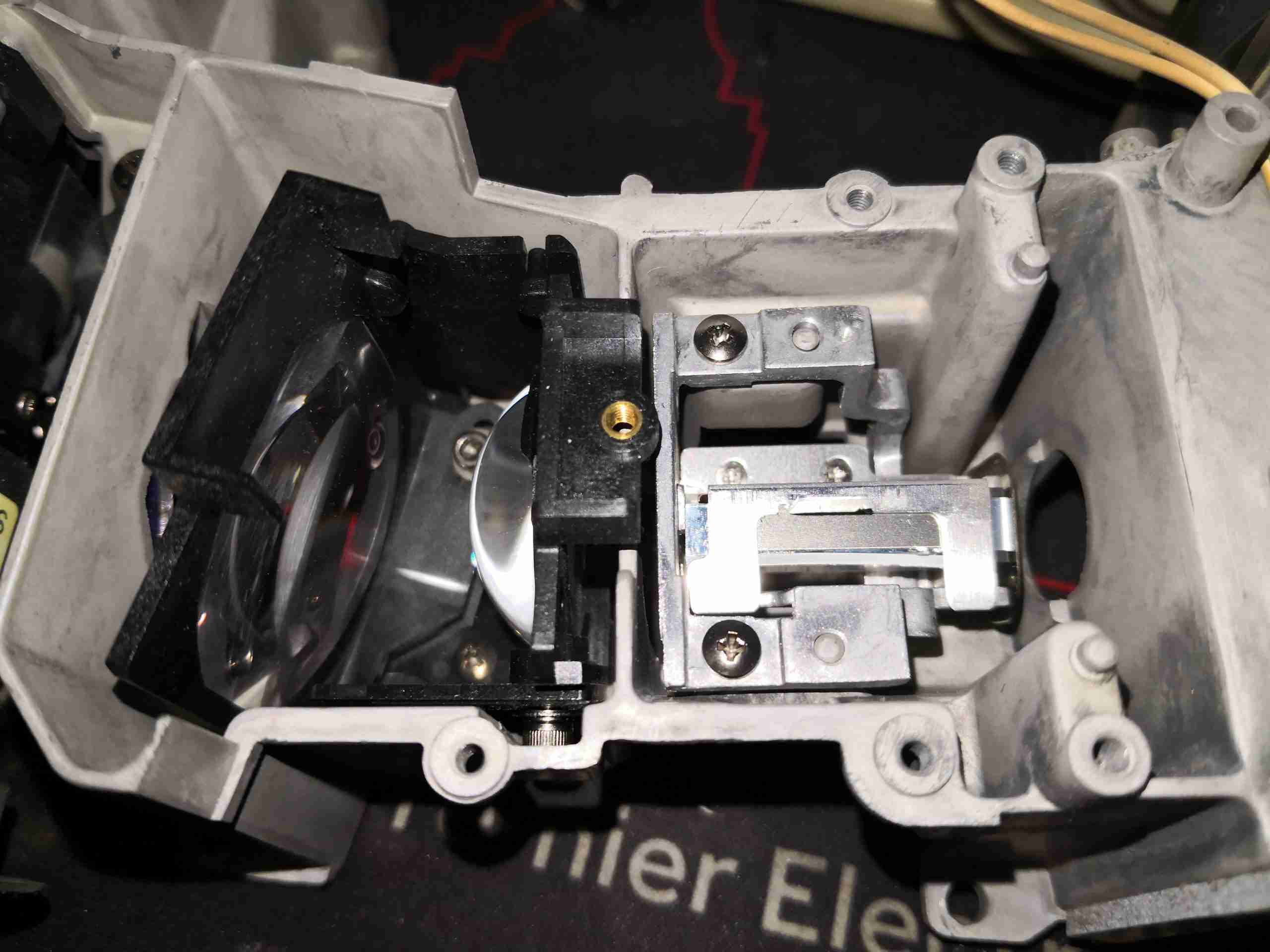
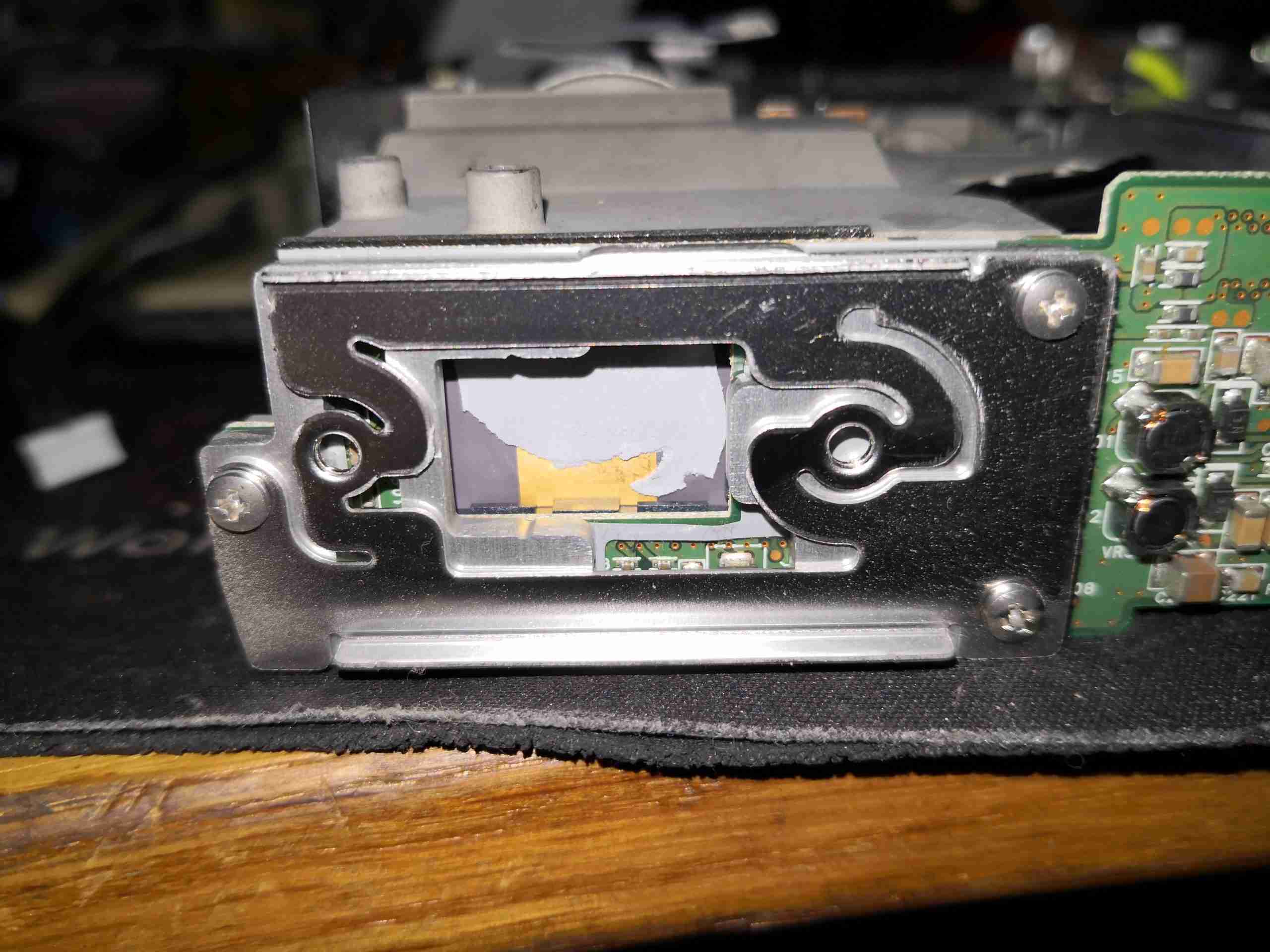
Light Engine
A closeup of the light engine shows the back of the phase sensor for the colourwheel, and the mounting brackets for the optics.
Colourwheel
The dichroic colourwheel is tucked into the gap between the lamphouse & the first optic.
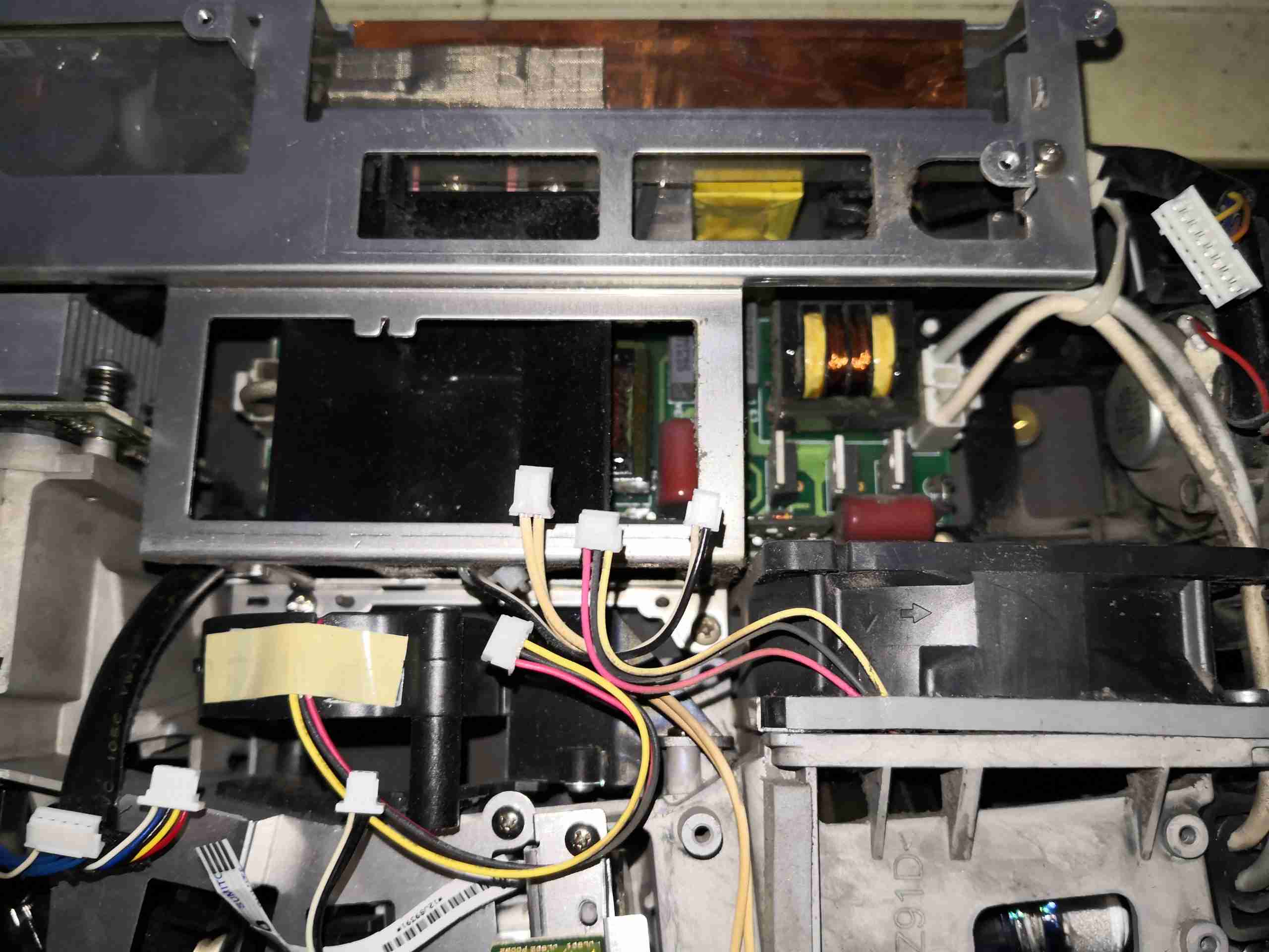
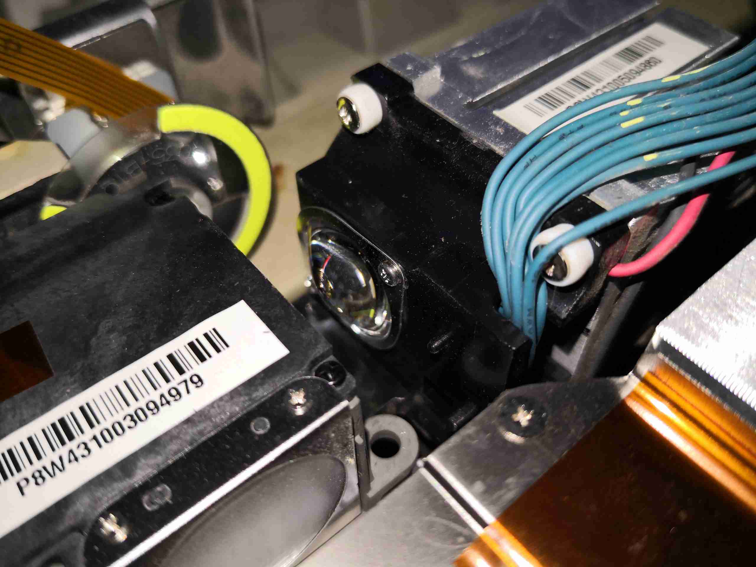
PSU Section
Hiding at the back of the projector is the alloy frame holding the power supplies & cooling ducts.
DC PSU & Lamp Ballast
After removing the brackets, the DC power supply & the lamp ballast are visible. Since this projector uses a UHP arc lamp, the DC power supply which has the usual low voltage outputs for the logic board, has an auxiliary output from the +340v rail after the PFC circuit that supplies power to the lamp ballast.
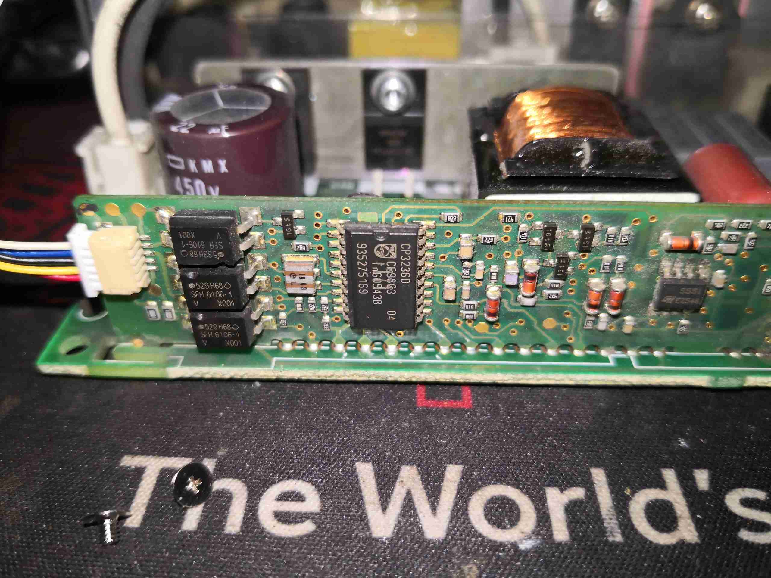
Lamp Ballast Control PCB
The lamp ballast is a pretty standard design, using an Osram control board.
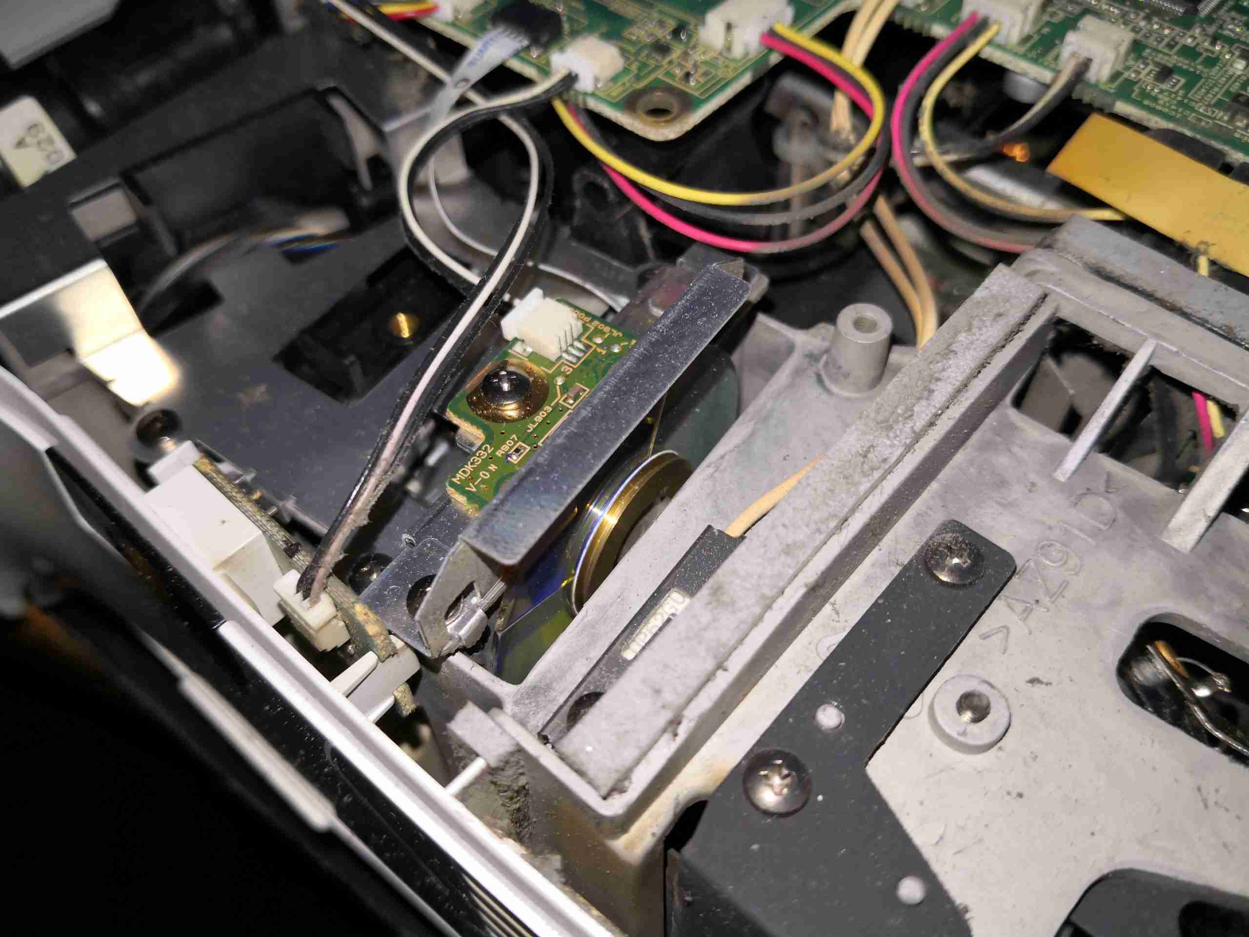
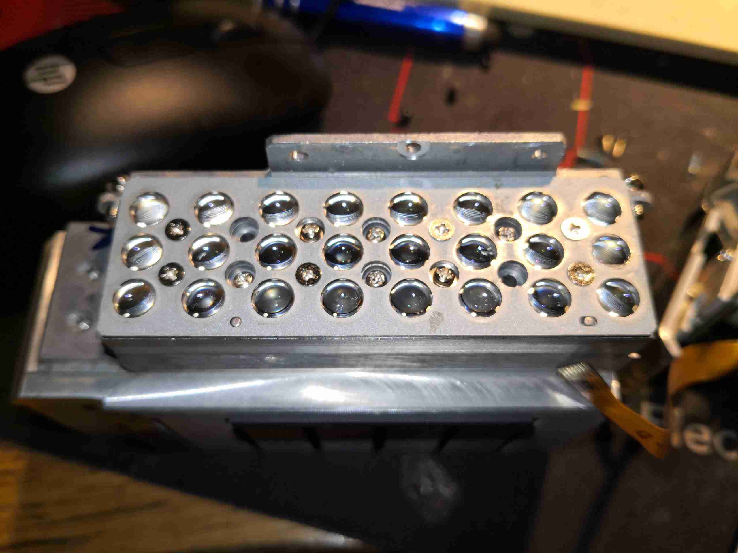
Homogeniser & Lenses
After removing the top cover with the colourwheel, the main optic chain is visible. The usual mirror tunnel homogenizer at the start, with a convex & aspheric lens on the left.
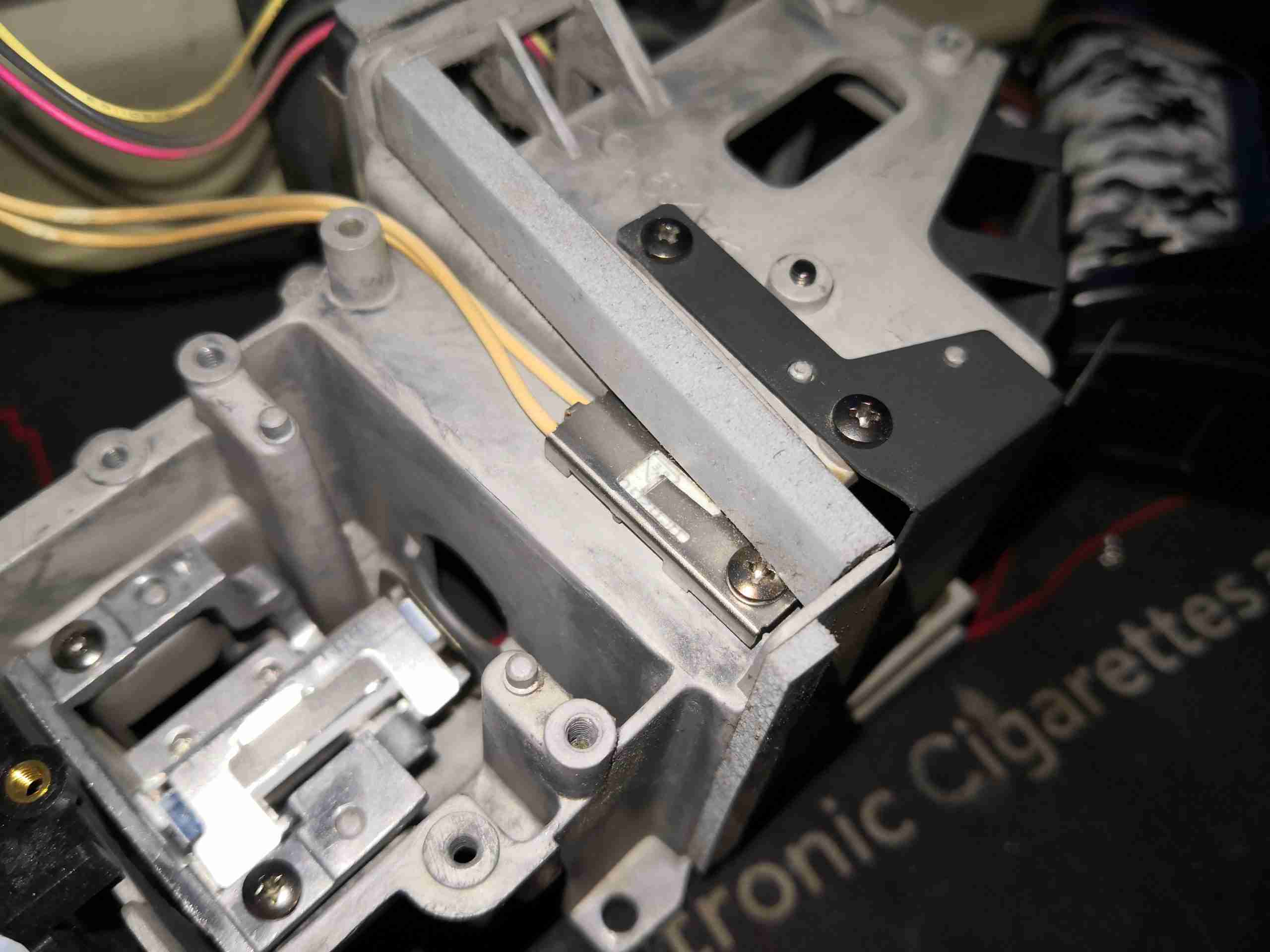
Lamphouse Thermal Cutout
The lamphouse has a last-resort thermal cutout to shut the ballast down if the cooling fans fail. These lamps output some serious heat, and likely wouldn’t last longer than a couple of minutes without cooling.
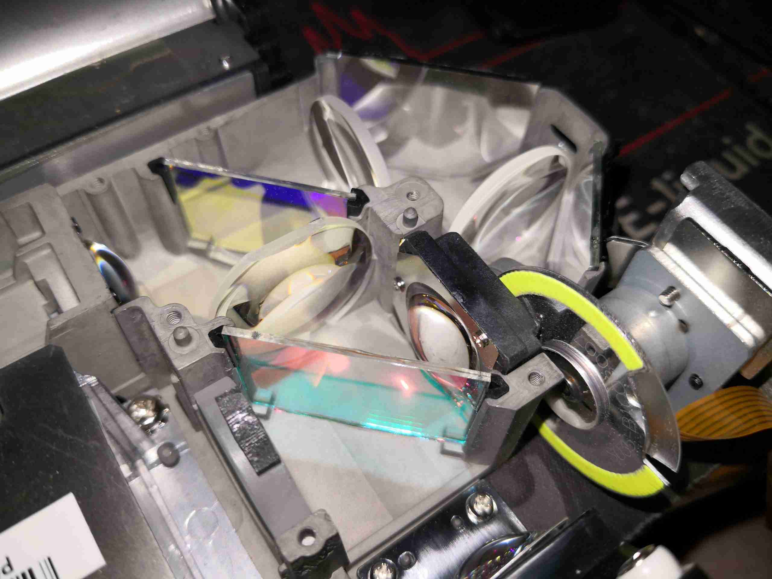
DLP Optics
The final turning optics before the DLP chip are hidden in the Mg casting of the light engine.
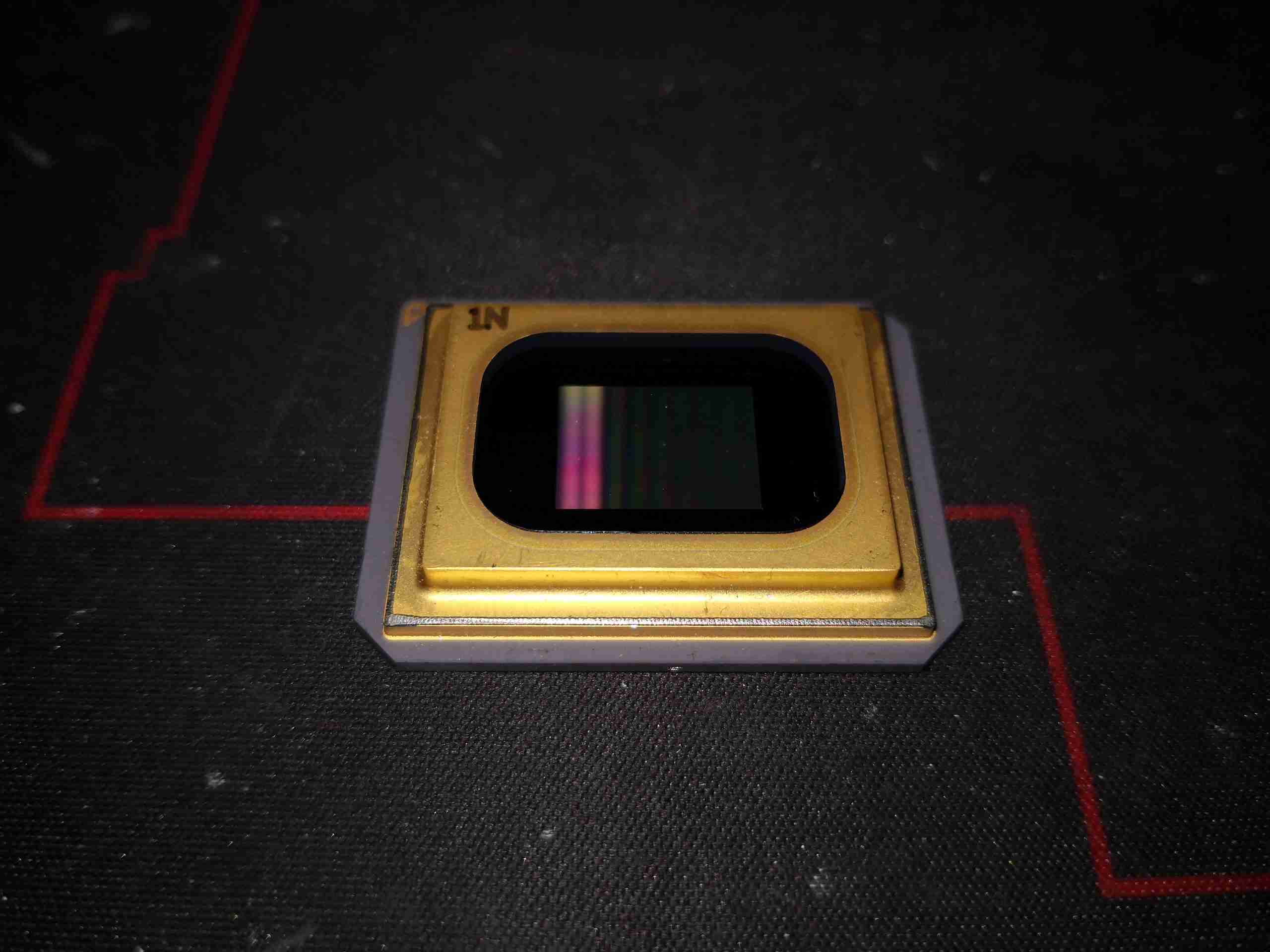
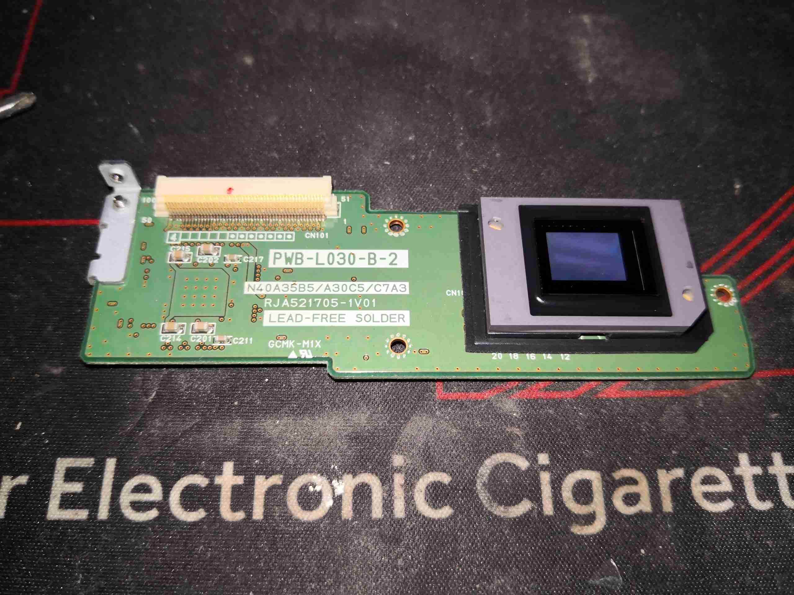
DLP
The DLP is the older type, with the large ceramic LGA package.
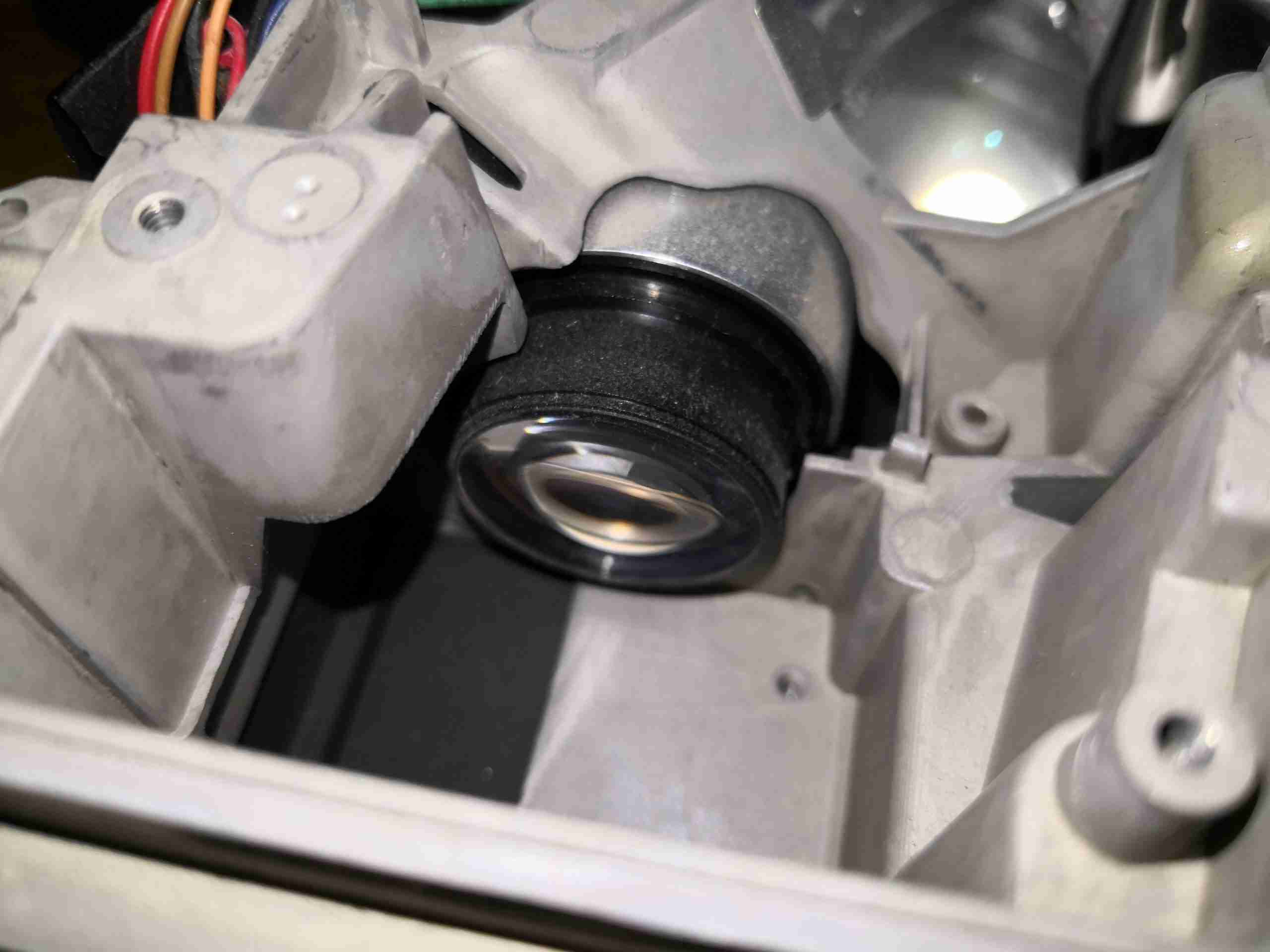
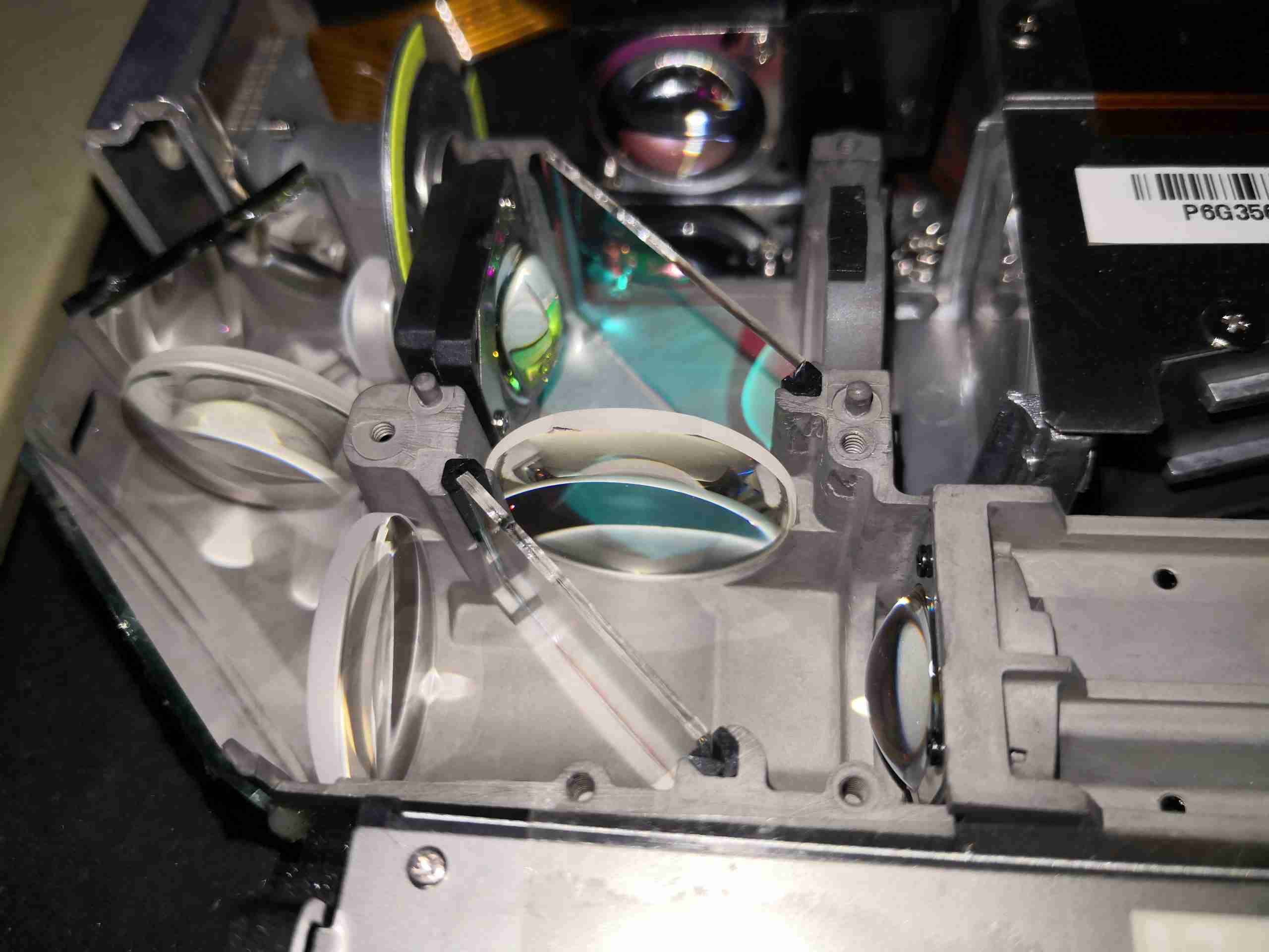
Projection Lens
After the DLP, the light is routed through the objective lens, to the screen. This is the back of the lens inside the light engine.
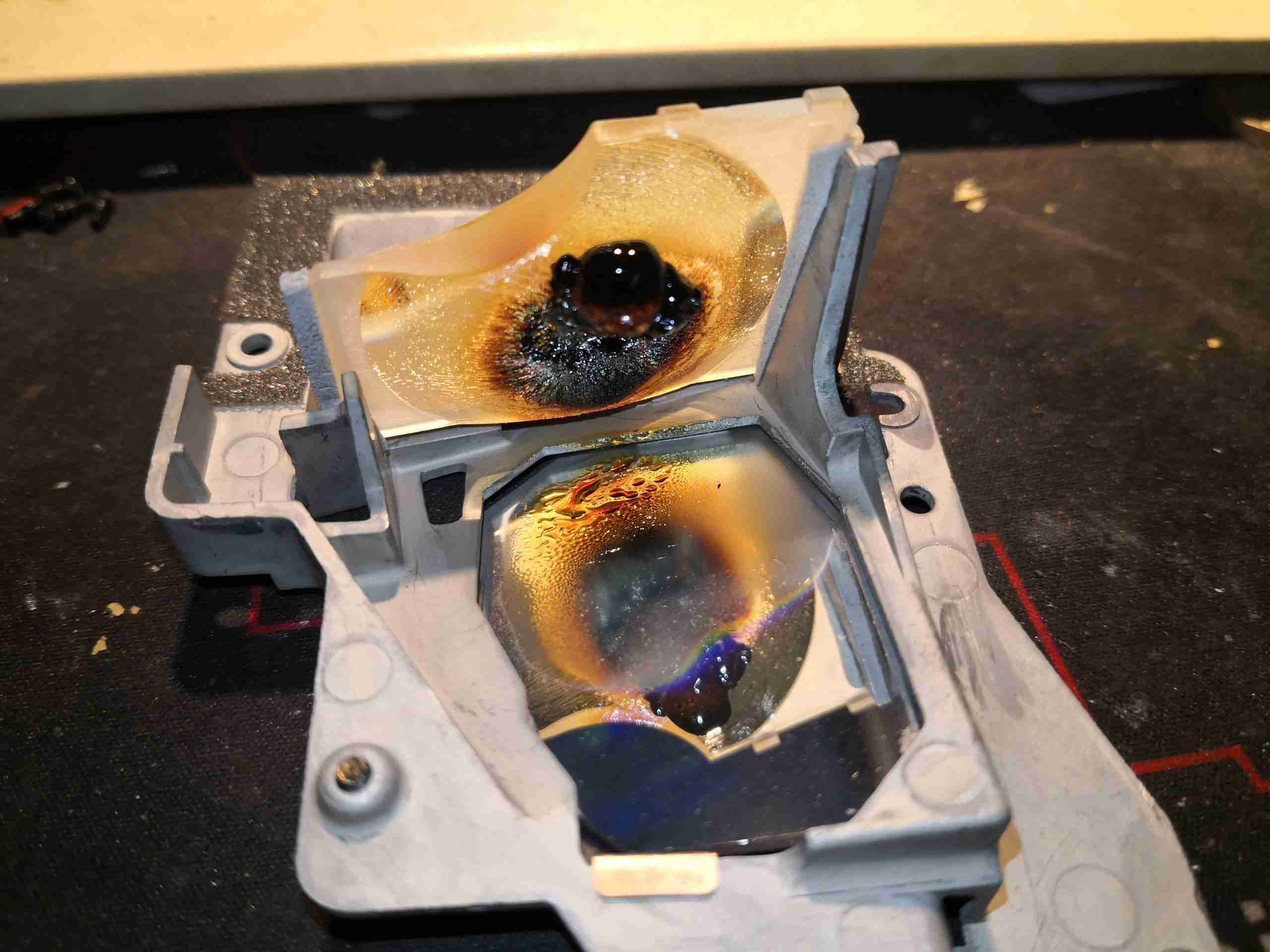
Failed Optic
And here is the main problem with the projector – the last lens in the optical chain before the DLP chip has been roasted by the intense light flux from the lamp. Unfortunately NEC cheaped out on this one – it’s the only optic in the machine that isn’t made of glass. This was likely caused by some contamination on the lens, which starts the process of absorbing light on the surface. The resulting heat then causes discolouring of the lens, which absorbs more heat. A chain reaction ensues, ending in the lens completely destroying itself.
Autofocus
The projection lens has a couple of sensors, for the focus & zoom, along with a focus motor. This is driven by feedback from a distance sensor in the base so no manual focusing is required.
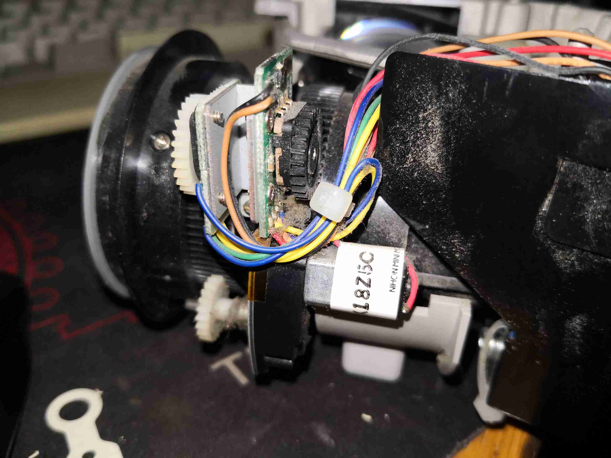
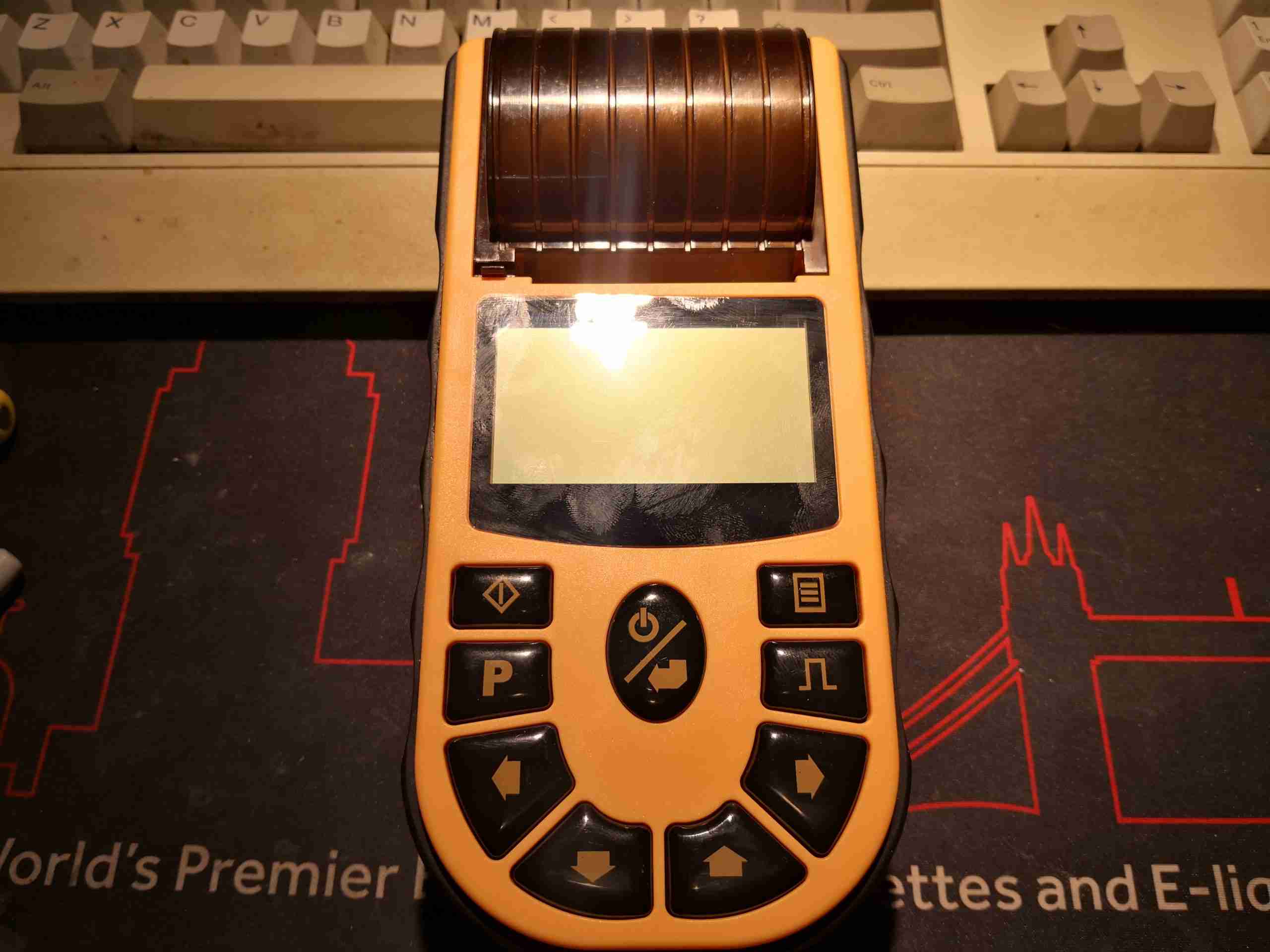
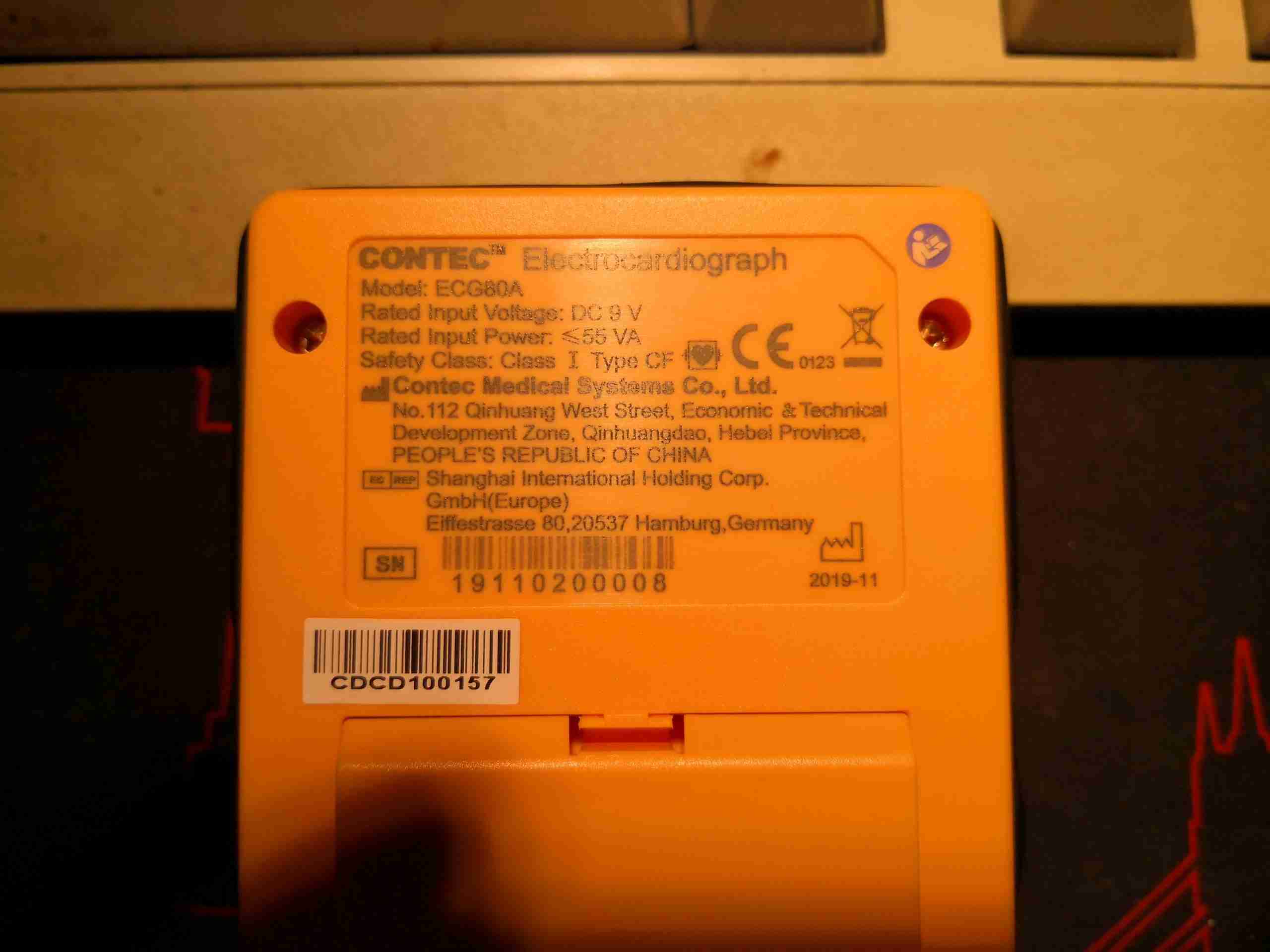
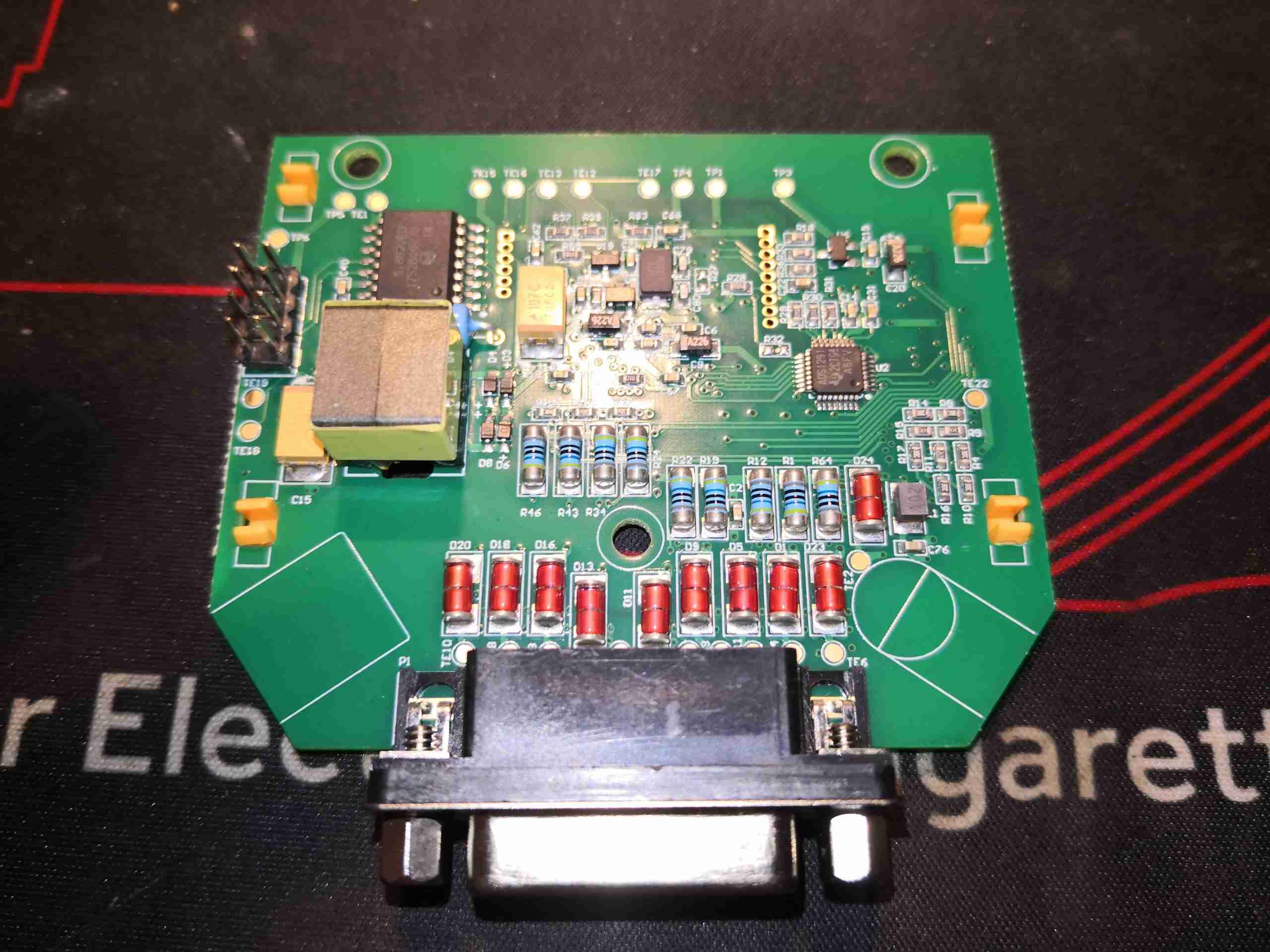
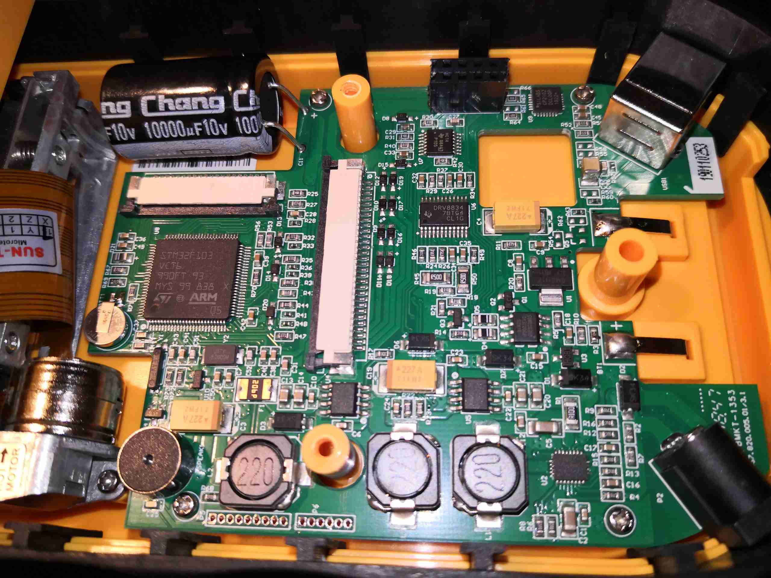
I figured it was about time I added to the medical kit, and since Contec, who makes my SPO² meter seems to have a decent level of manufacturing quality, one of their ECG machines seemed like a good choice. This is the ECG80A handheld Electrocardiograph. This is a single channel, 12 lead unit – meaning it’s a full 12 lead ECG, but it records one lead at a time, in sequence.
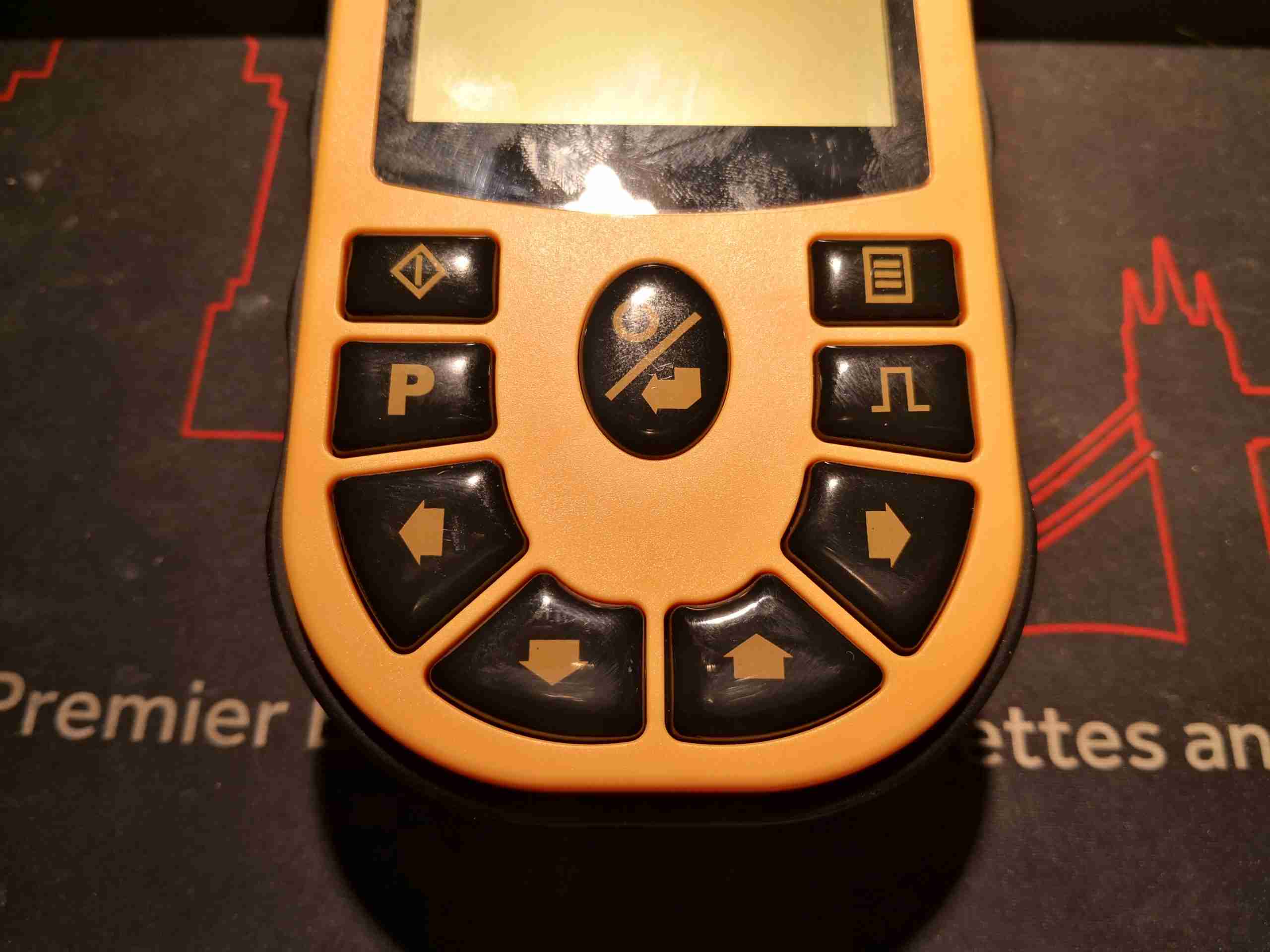
Control Buttons
Control is via the front panel, with some large buttons.
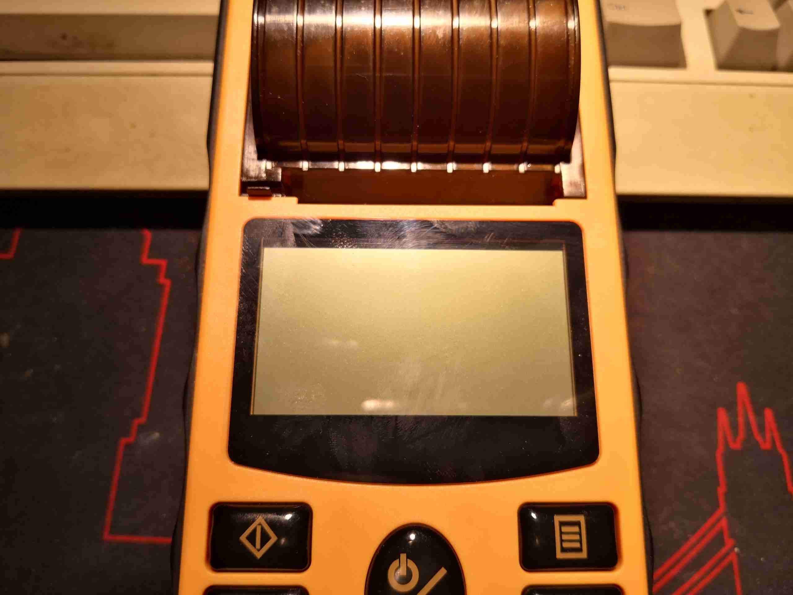
LCD Display
Readout is provided on a dot-matrix LCD, which is brightly backlit. There’s a thermal printer for rhythm strips, printing onto 50mm wide paper rolls.
Labelling
The rear has the laser-marked rating plate, with all the specifications & regulatory markings. From the serial numbering, it looks like my unit was manufactured on 3/11/19, and was the 8th unit off the production line. Underneath can be seen the top of the battery pack, which just clips into place. There aren’t any markings on this at all, but I do know from the manual it’s a 7.4v 2S Li-Ion pack, energy capacity is another unknown, but there is very little weight to the battery, so it can’t be that large.
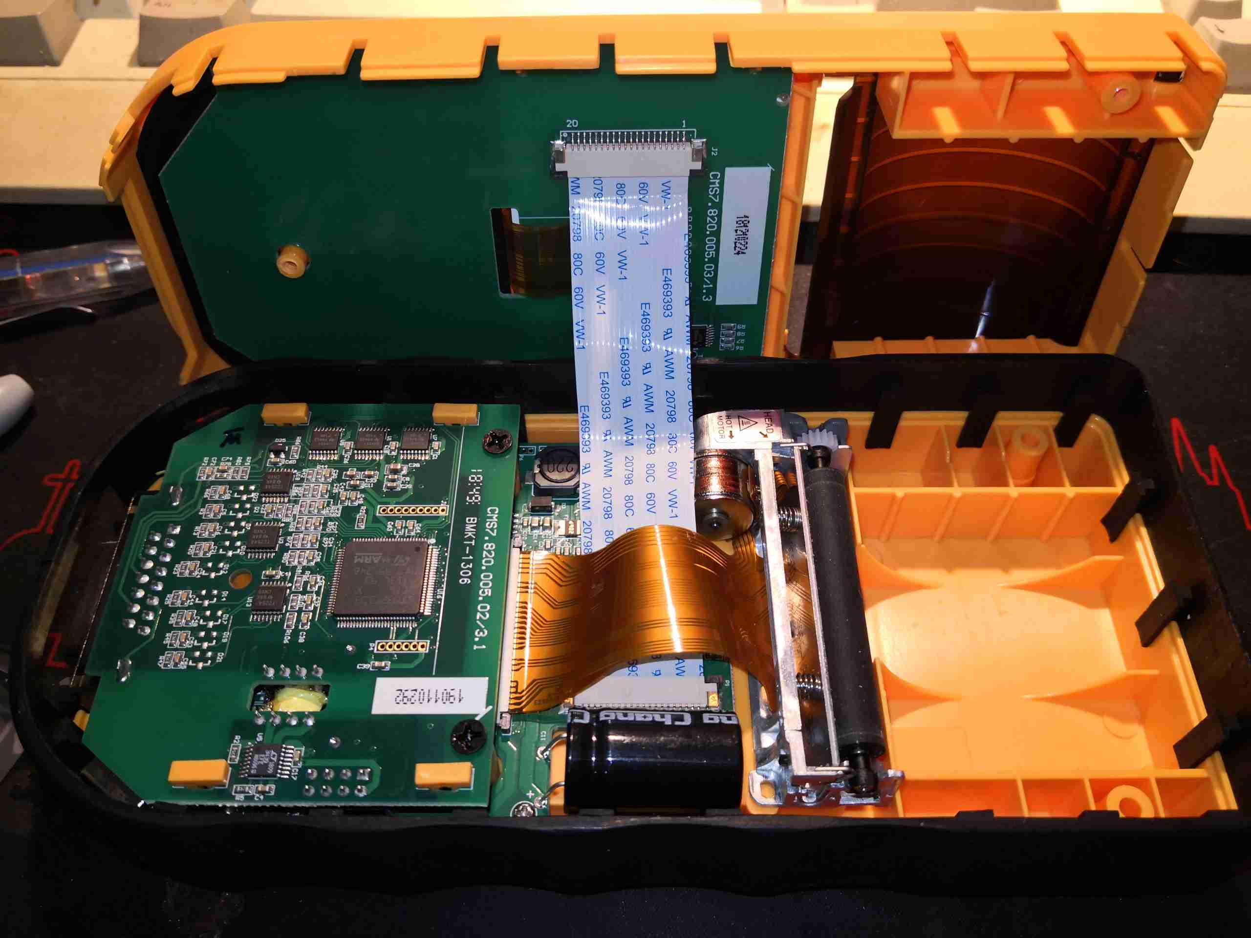
Internals
3 Philips screws hold the unit together, and once those are removed, the shell halves separate. The FFC to the LCD & button pad is currently keeping things connected together.
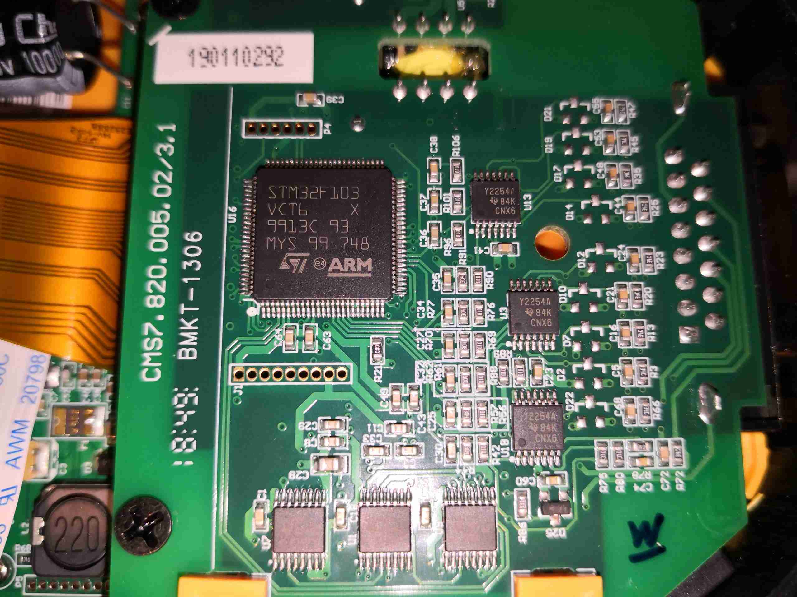
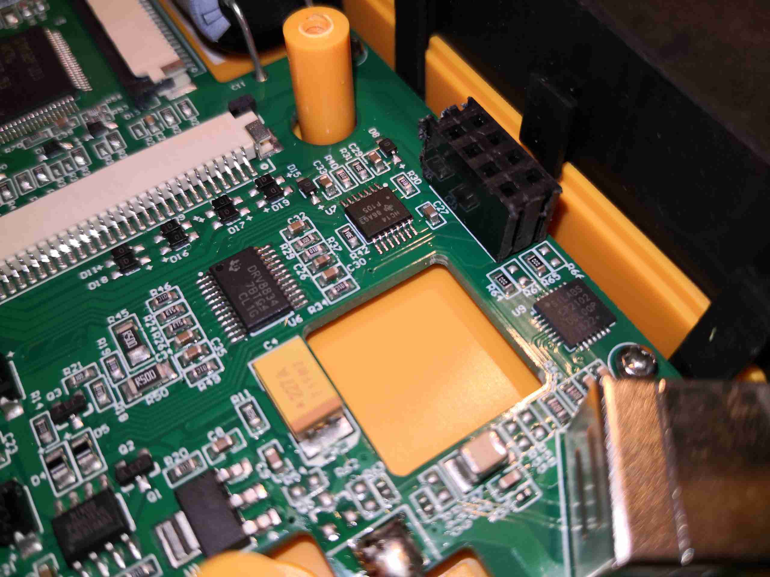
Acquisition PCB
The first of 3 PCBs inside the shell is the acquisition PCB, with all the patient-connected circuitry. The DB-15 connector is on the right hand side, where the ECG leadset connects.
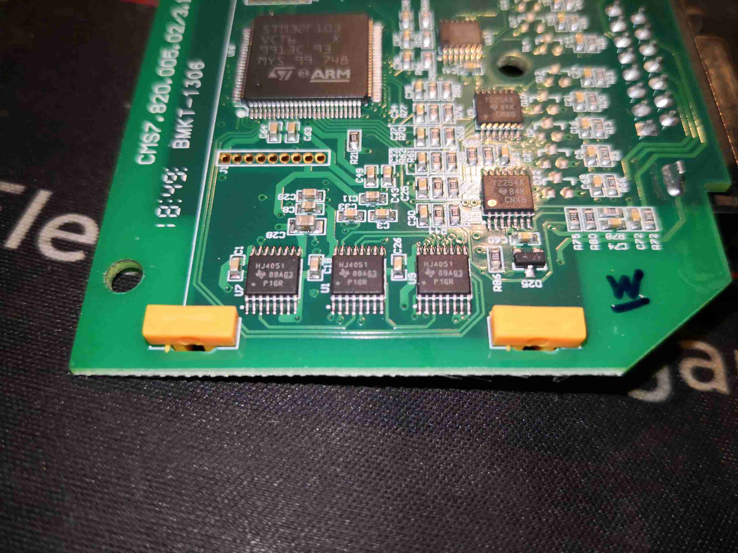
Signal Switching
The bottom edge of the PCB has a trio of HJ4051 high speed analog multiplexers, which are switching the ECG leads onto the Ultra-Low Power Op-Amps on the right, a trio of TCL2254A devices from Texas Instruments, before being sent on to the ADC.
Acquisition PCB Bottom
The bottom of the PCB has the DB-25 connector, along with the input protection diodes & resistors. This array of protection components serves two purposes – protection of the instrument against defibrillator voltages & protection of the patient from electrical shock by the instrument.
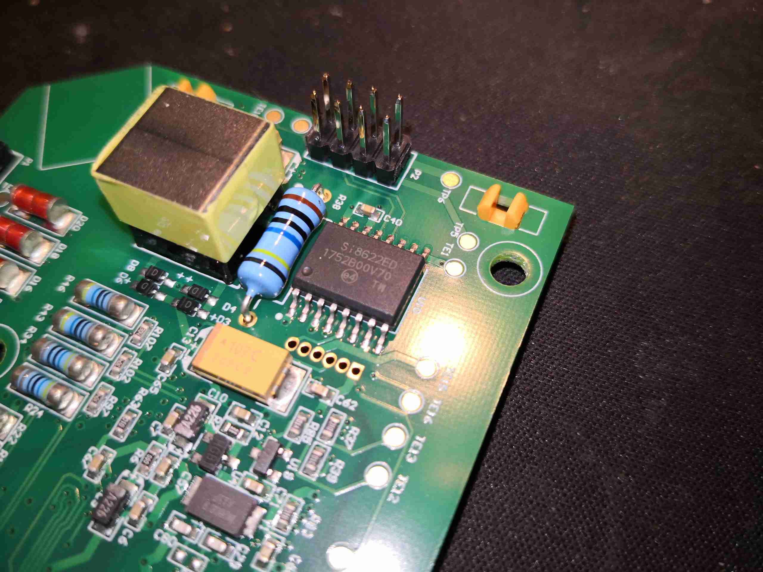
Signal Isolation
A 5kV isolation barrier is provided between the rest of the unit & the acquisition board, both for the data path & power path. The isolation transformer is visible on the left here, next to the 8-pin header that connects to the main PCB. There’s a 100MΩ resistor across the isolation barrier, probably for ESD bonding. To the right of that is a SiLabs Si8622ED single channel digital isolator IC.
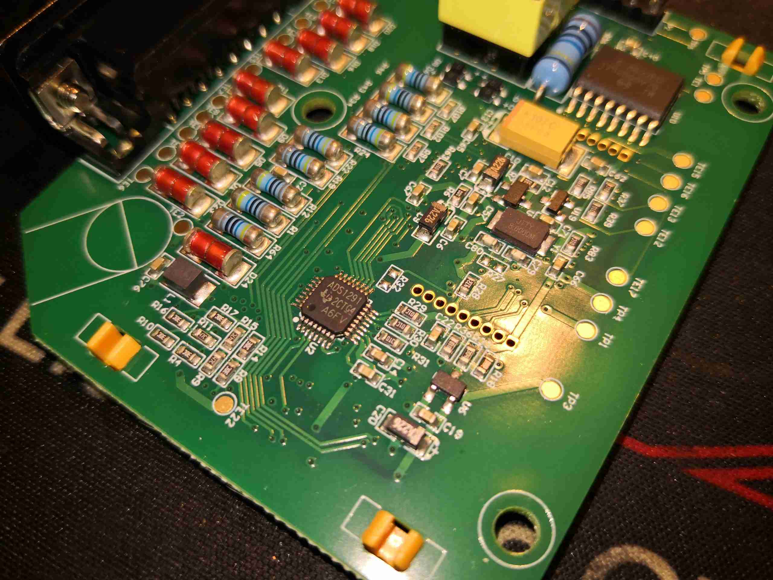
ADC
The final bit of conversion of the input waveform is performed by a Texas Instruments ADS1291, a 2-channel 24-bit Analogue front-end specifically designed for Bioelectrical measurement such as ECG. This contains a ΔΣ ADC, and a pair of Programmable Gain Amplifiers on the input, together with some multiplexing. This communicates via SPI to the host microcontroller.
Isolated Power Supply
Power is transferred across the isolation gap through the transformer, driven by a Linear Tech LT3439 slew-rate controlled ultra low noise isolated switching supply driver.
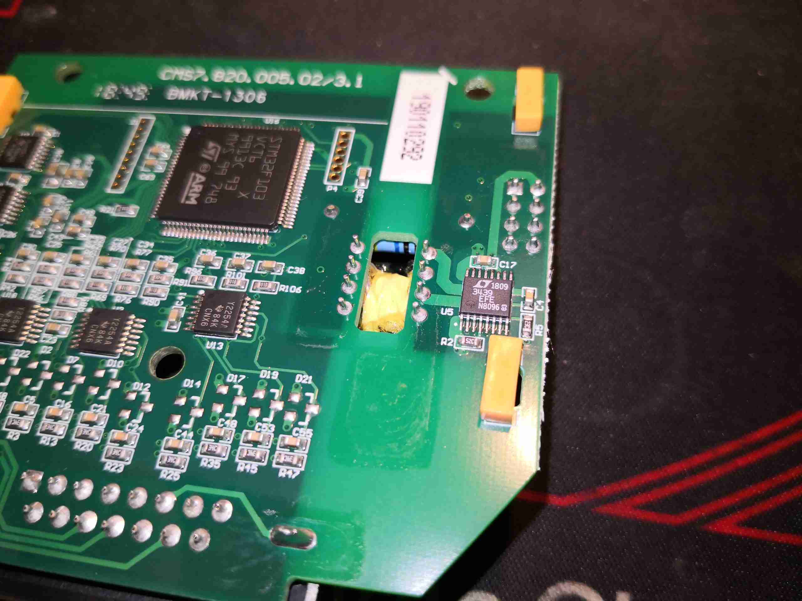
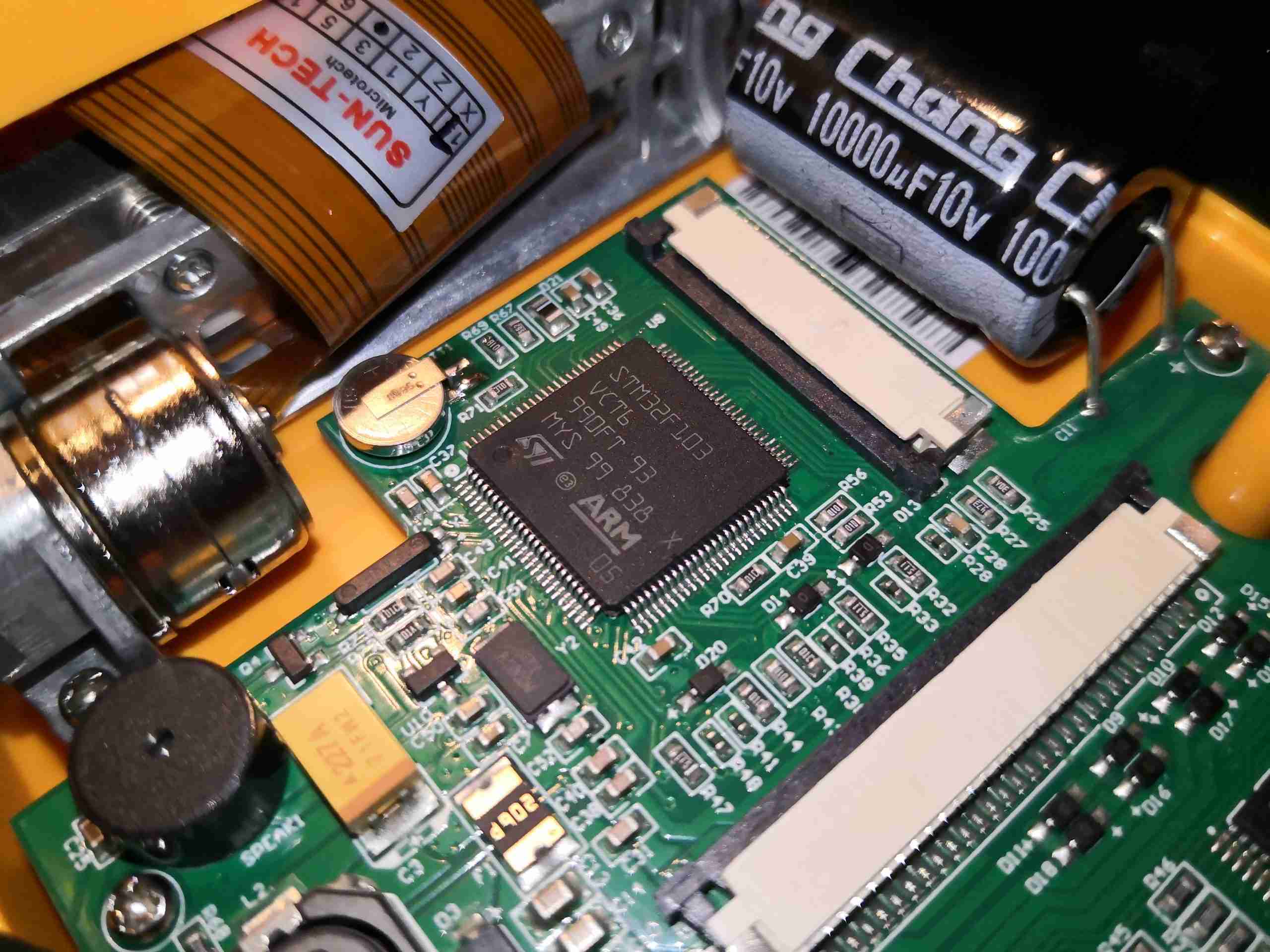
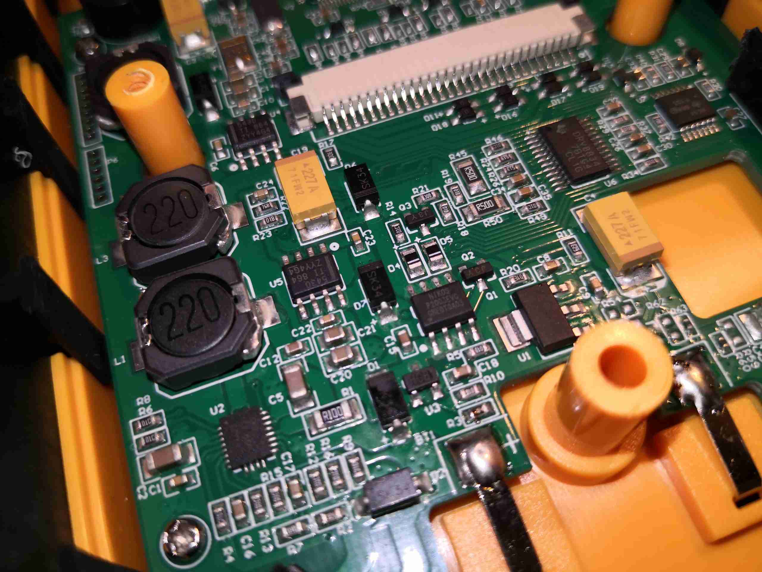
Mainboard
Underneath the acquisition board is the main PCB itself, with the rest of the support electronics. On the lower edge of the board are the power supplies, the main microcontroller on the left, another STM32F103, USB Serial communications top right, and DC input bottom right.
Main CPU
Here’s the main microcontroller with it’s support components. This will be receiving a datastream from the acquisition microcontroller, probably I²C considering the single-channel digital isolation, and further decoding this for either display on the LCD, printing on the thermal paper or sending as a datastream over USB Serial to a PC.
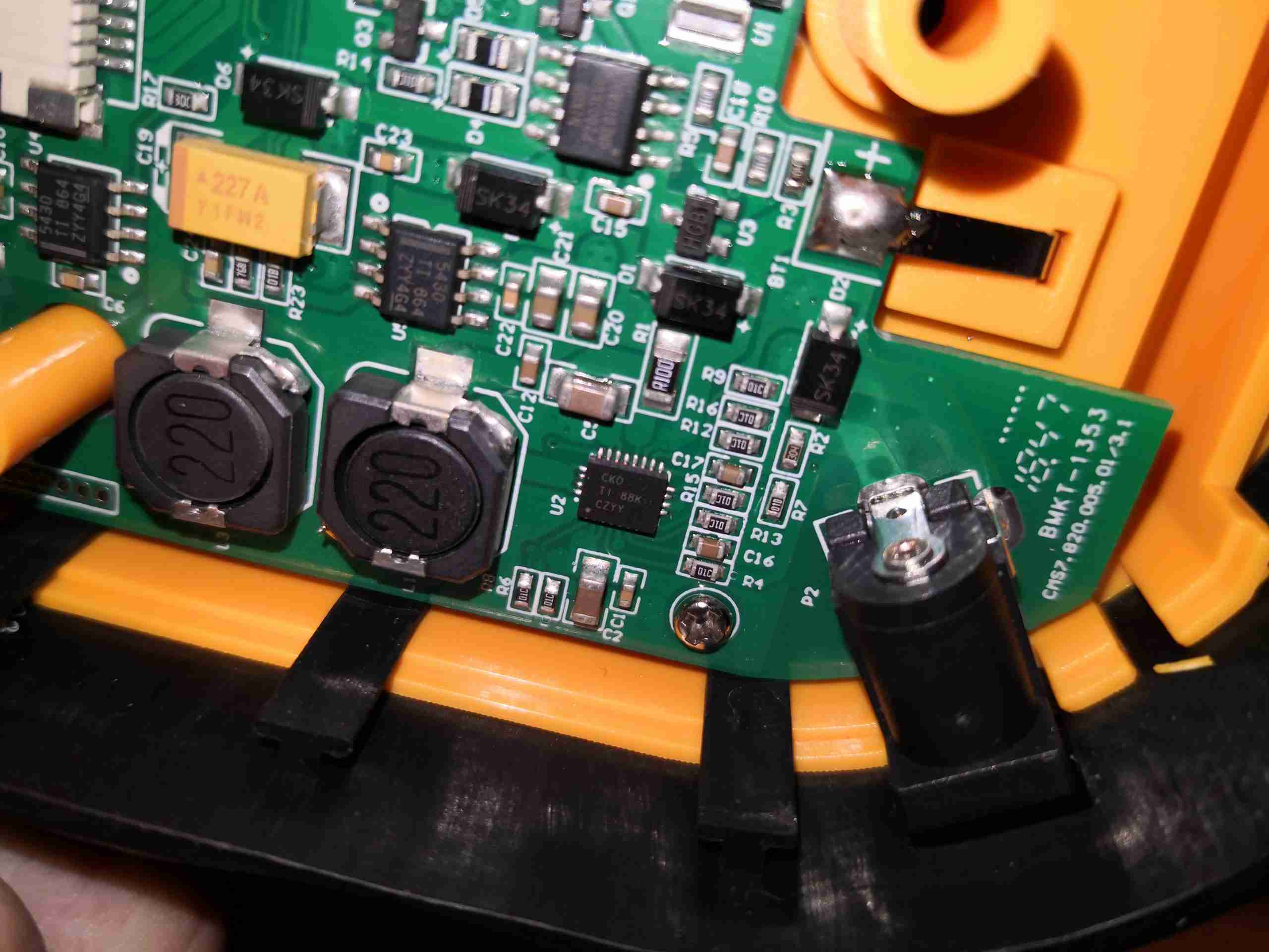
Power Supplies
The onboard 2S 7.4v Lithium Ion battery is handled by a Texas Instruments bq24103A Synchronous switched-mode charge management IC here, just to the left of the barrel jack. It’s inductor is just to the left of the IC. This is a fairly nice chip, with support for up to 3 series cells with full auto sensing.
DC-DC Converters
Other power supply rails are dealt with via a pair of TPS5430 buck converters, again from TI. Their associated inductors are along the left side of the board. There’s also an LM1117-3.3 linear regulator for a low-noise supply, possibly for the microcontroller power rail. There’s also a few discrete switching components, and a DRV8834 bipolar stepper driver for the printer.
USB Interface
Finally, in the corner of the board is the USB connector, with a SiLabs CP2102 USB UART IC. This interface is used with the optional PC Software. The routed hole in the PCB is clearancing for the isolation transformer of the acquisition board.
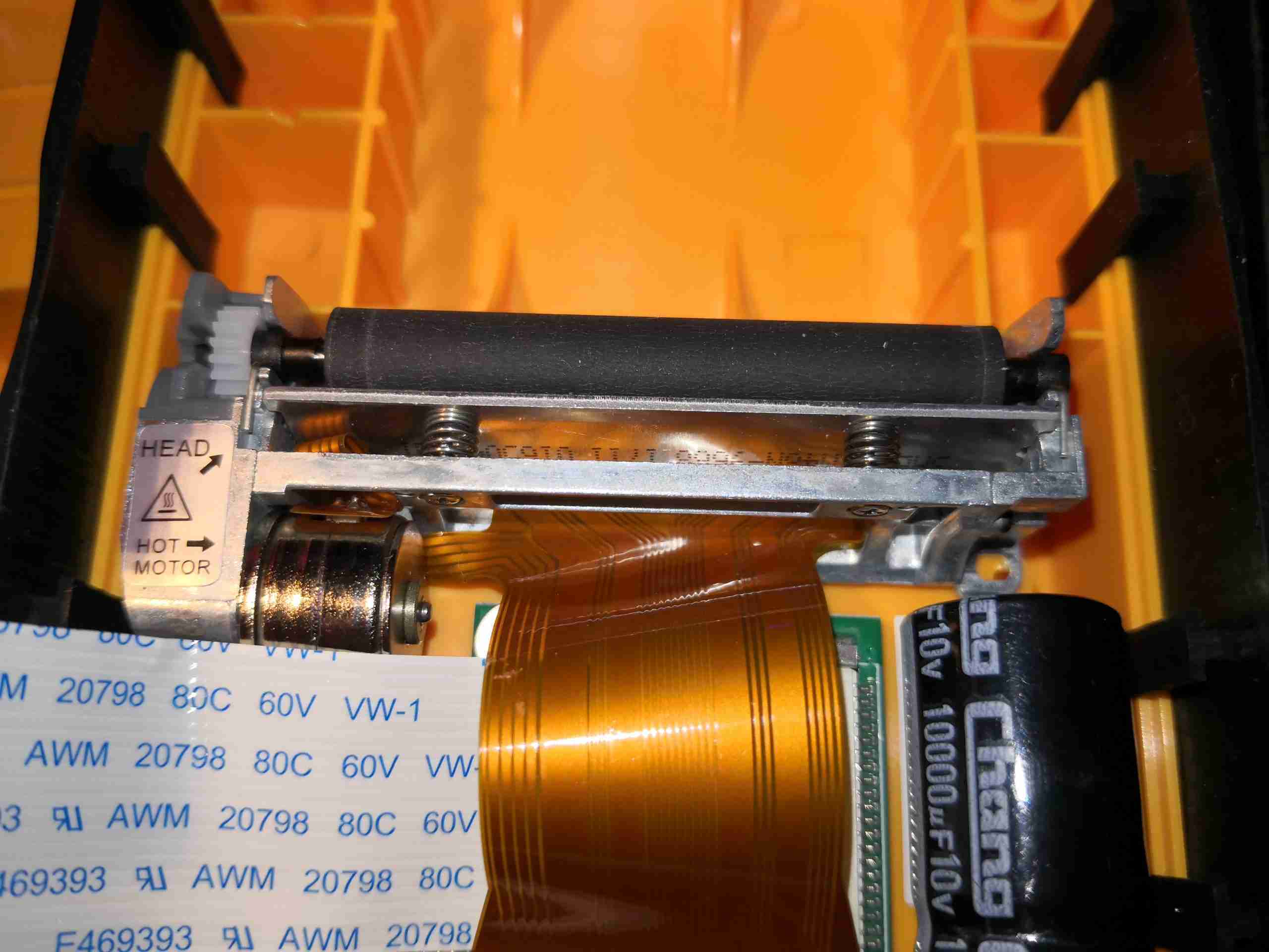
Printer Module
Here’s the printer module, at the top of the shell. There’s a tiny stepper motor on the lower left that moves the paper past the print head, which is the bar mounted on springs across the centre. The odd thing with this is to load the paper, the black rubber pinch roller has to be completely removed from the printer, the paper placed across the print head, and the roller clipped back into place – instead of the roller being mounted on the front cover like on most thermal printers.
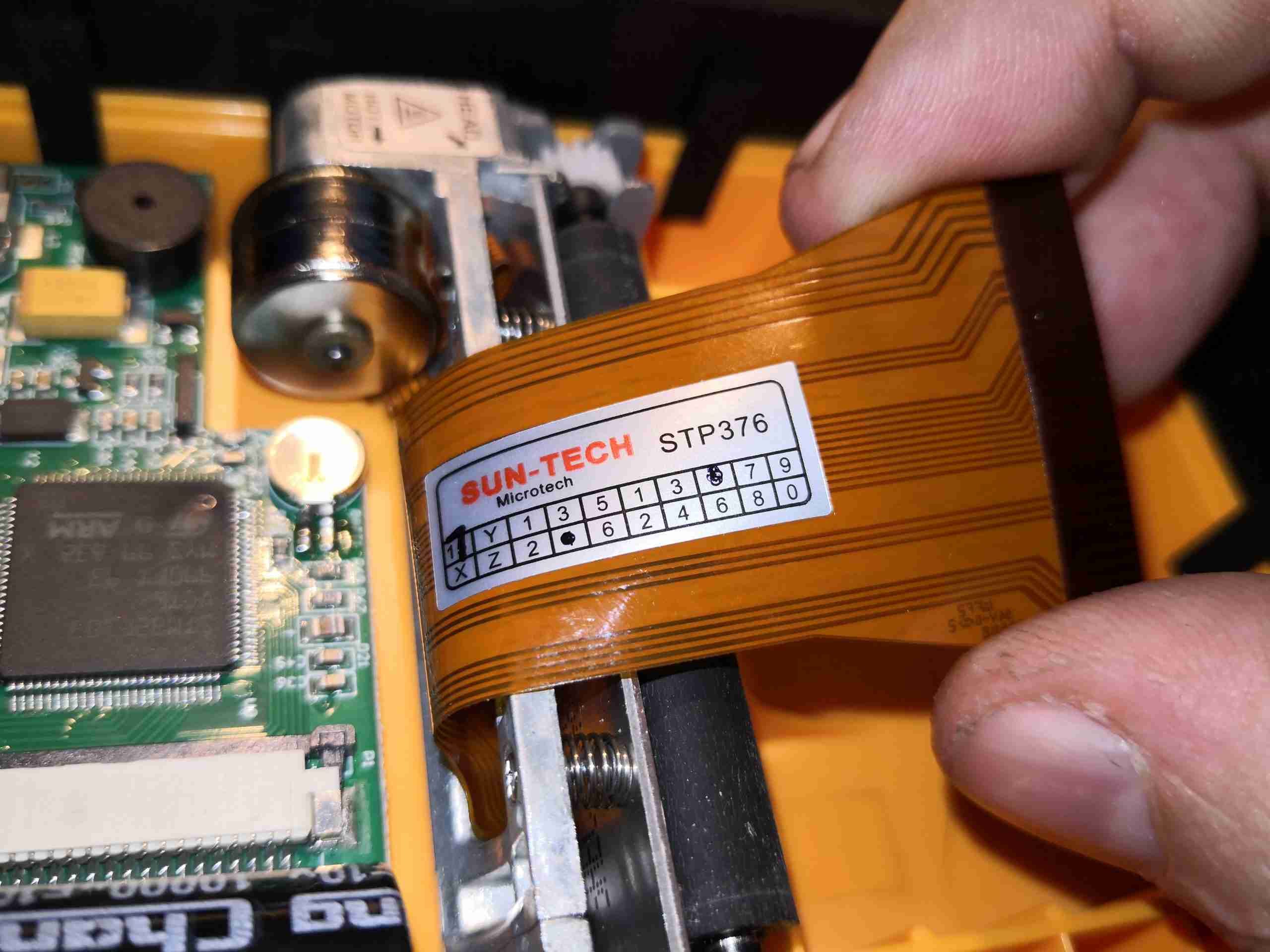
Printer Label
The printer module is manufactured by Sun-Tech, the STP376. I’ve not managed to find any information on this at all, either the manufacturer, or the part number. I did find a SunTech, in the medical sector, but their logo is very different from the labelling here.
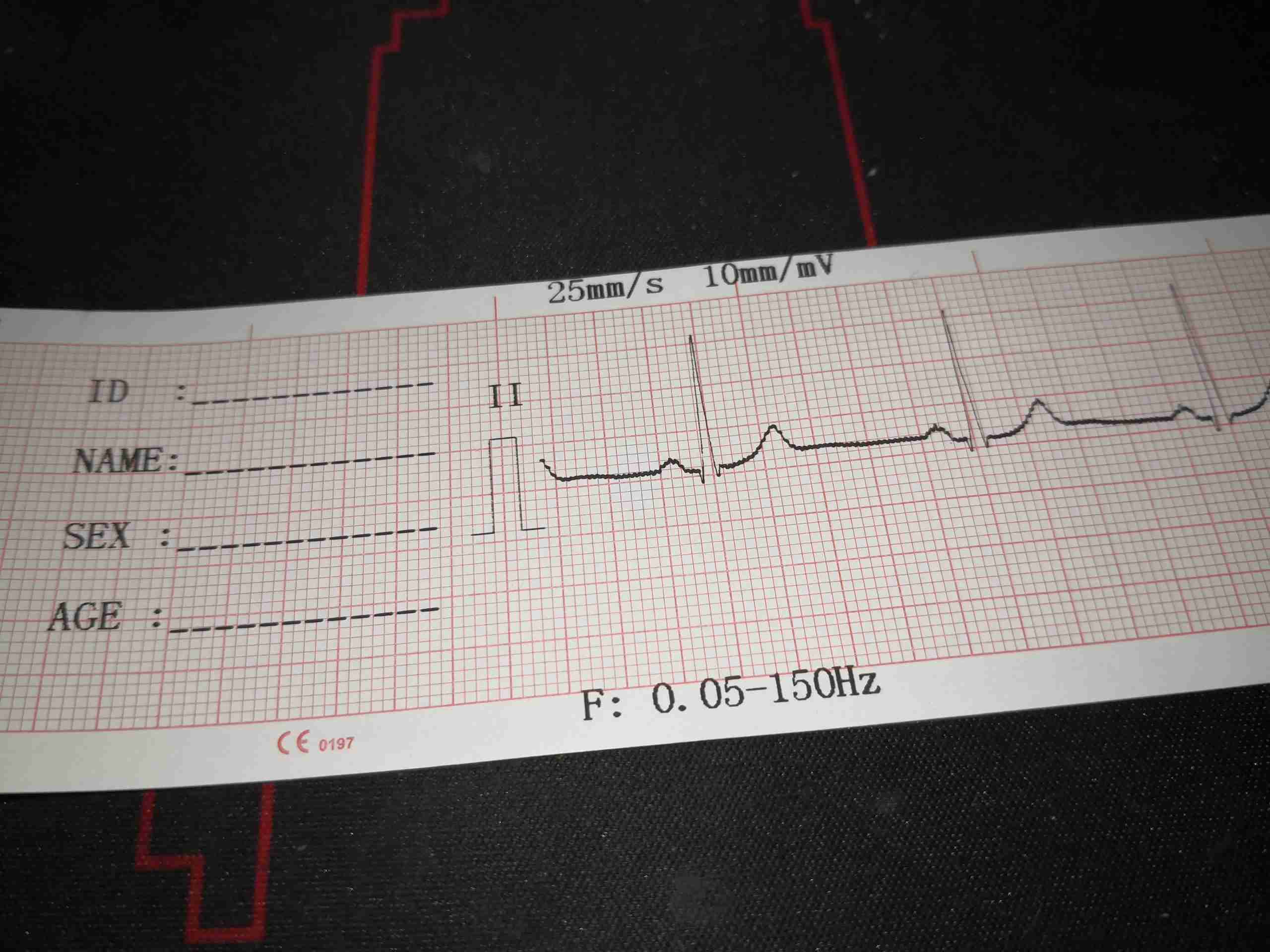
Lead II Example Printout
Here’s an example of the print quality of the unit, which just so happens to be lead II taken from me! It’s pretty good overall, with nice clear printing. There is a little interference on the trace that can be seen, but that’s not the ECG’s fault – this trace was obtained in a relatively EMC-noisy environment. The unit first prints a section for patient details, then the lead ident & 1mV calibration mark, then the actual trace. Machine settings are printed in the top & bottom margins, showing the print speed, sensitivity setting, and any applied frequency settings. There is a little bit of interference on the A full 12-lead printout is roughly 3 seconds per lead in sequence, and takes up about 1.2m of paper at standard 25mm/s speed setting.
It recently became rather obvious there was something amiss with the water heater on board nb Tanya Louise – lots of smoke from the exhaust, failed starts, and finally a total refusal to start altogether.
Combustion Chamber
On disassembly, it was clear the burner was the issue – above. The mesh at the back where the fuel inlet enters the burner is completely knackered. The burner in these heaters, like the Eberspachers, is evaporative. Diesel fuel is led into a high-surface area mesh tube, or pad in this case, where it is vaporized to be burned with air from the combustion blower. Initially, this heat is provided by the glow plug, but after the unit has fired, the heat of combustion keeps the process going.
Burner Deposits 1
As can be seen at left, there’s quite the build-up of solid carbon around the burner, blocking most of the mesh & the air mixing holes in the tube. This was also after I’d removed most of the fouling!
Burner Deposits 2
More deposits are seen on the other side, along with some of the air mixing holes.
Inlet Plate
Now, the problem is that these burner units are not meant to be refurbished. These units are considered by the manufacturer to be disposable, and are welded together as a result. There’s another issue – I don’t believe that a component costing around £295 in a service kit as DISPOSABLE. There’s nothing wrong with the structure of the burner at all – it’s Stainless Steel, and is in good shape with no heat damage. The only fault is with the mesh being burned out from long use. Luckily, replacement burner meshes are available on eBay from Chinese suppliers, so on with the repair! One of the welds that needs to be removed can be seen here next to the glow plug well, and there are 3 spots around the rim that are welded in this way. Delicate use of a grinding wheel on the welds allows this to be removed intact.
Burner Tube
Once the welds have been ground off, the fuel inlet plate with the mesh can be pulled from the back of the burner. It’s a good idea to add some registration marks to both pieces before they’re separated, so they can be put back together in the same orientation – required for both the glow plug wiring, and the fuel inlet tube to line up with the hole in the heater housing. The ring of slots visible around the edge of the tube are the combustion air inlets, and the air is directed through a ring of holes in the combustion chamber, quite similar to a turbine engine combustor.
Old Burner Mesh
Now I’ve got the back of the burner removed, the clogging is much easier to see. The mesh itself has clearly been subject to very high heat, and is partially burned away, along with most of the surface being clogged up with coal from incomplete combustion. It’s difficult to see here, but the mesh pad is held in place with a large circlip around the edge, all will become clear after cleaning. All the hard carbon needs to be scraped out of the cup, clearing the way for the clip to be pried out of it’s groove.
Cleaned Cup
After a lot of scraping with the sharp end of a small screwdriver, the cup has been relieved of enough carbon to be recognisable again! The fuel inlet tube is in the centre of the backplate, with the circlip groove around the edge. Crimp marks are visible on the top edge of the groove – I think Webasto actually crimps the ring in place after fitting, which does make removal a bit more tricky, but I did manage to get it out intact, even if heat has removed most of the heat treat from the steel – making it soft. Be careful here!
New Mesh Fitted
Fitting the new mesh is pretty simple. These have a sharp pressed side & a convex side, the convex side must face outwards from the cup. The circlip is visible around the edge of the mesh, with the ends next to the glow plug well. Make sure that the clip is equally spaced around the glow plug to make sure it doesn’t foul the plug when that’s replaced.
Now comes the issue of reattaching the cup to the back of the burner tube. I didn’t want to re-weld, since the assembly is Stainless Steel & I don’t have a TIG setup at present. I do have some stainless wire for the MIG, but this would also leave me with the issue of future disassembly if the mesh needs replacement again. Brazing is also not possible for the same reason – once brazed, it’s a permanent assembly.
Burner Reassembled
Since there are some tabs that were never welded, I decided to drill & tap M2.5 through these & use 304 stainless screws to hold the components together. This should allow removal in the future if required.
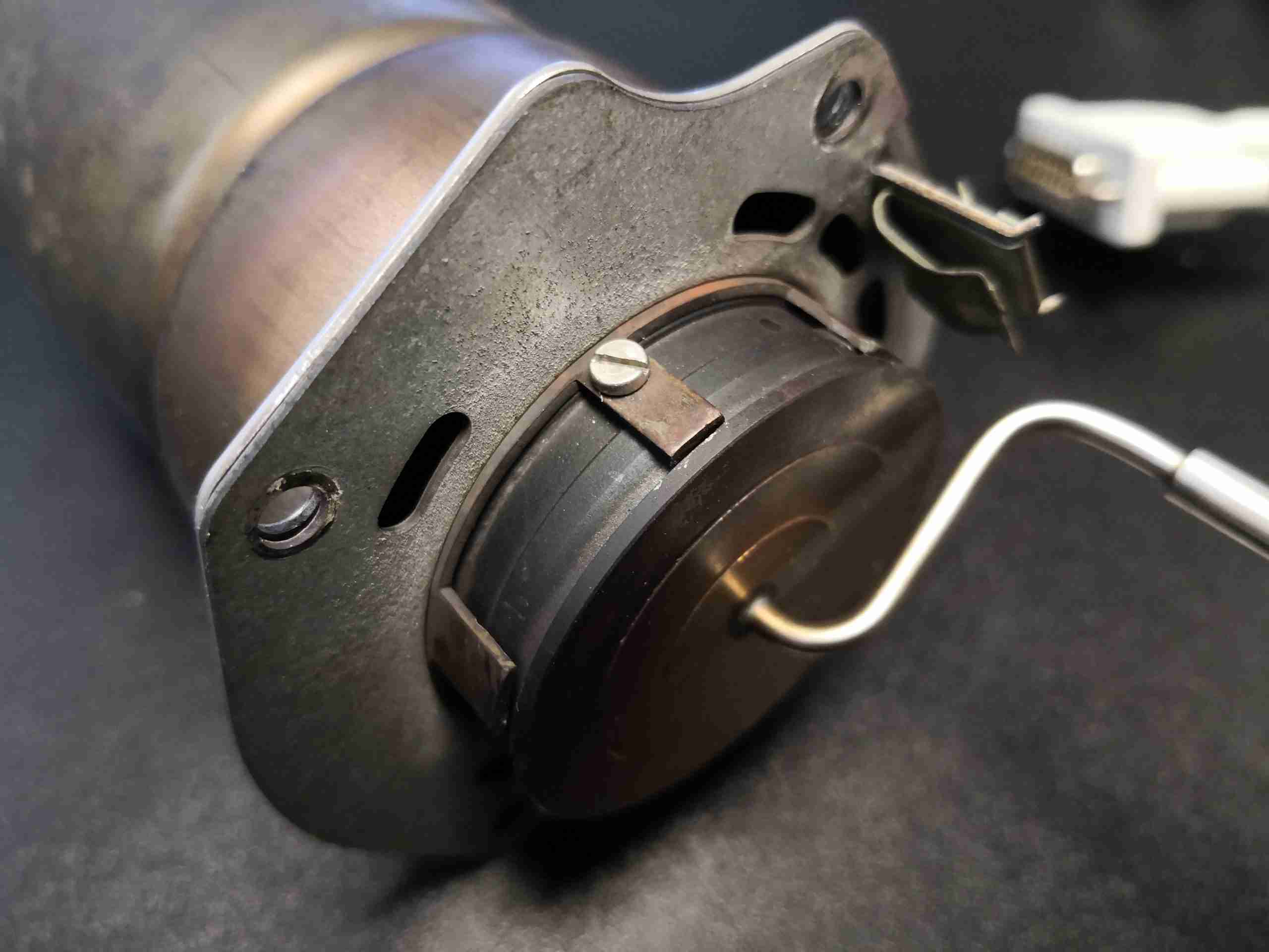
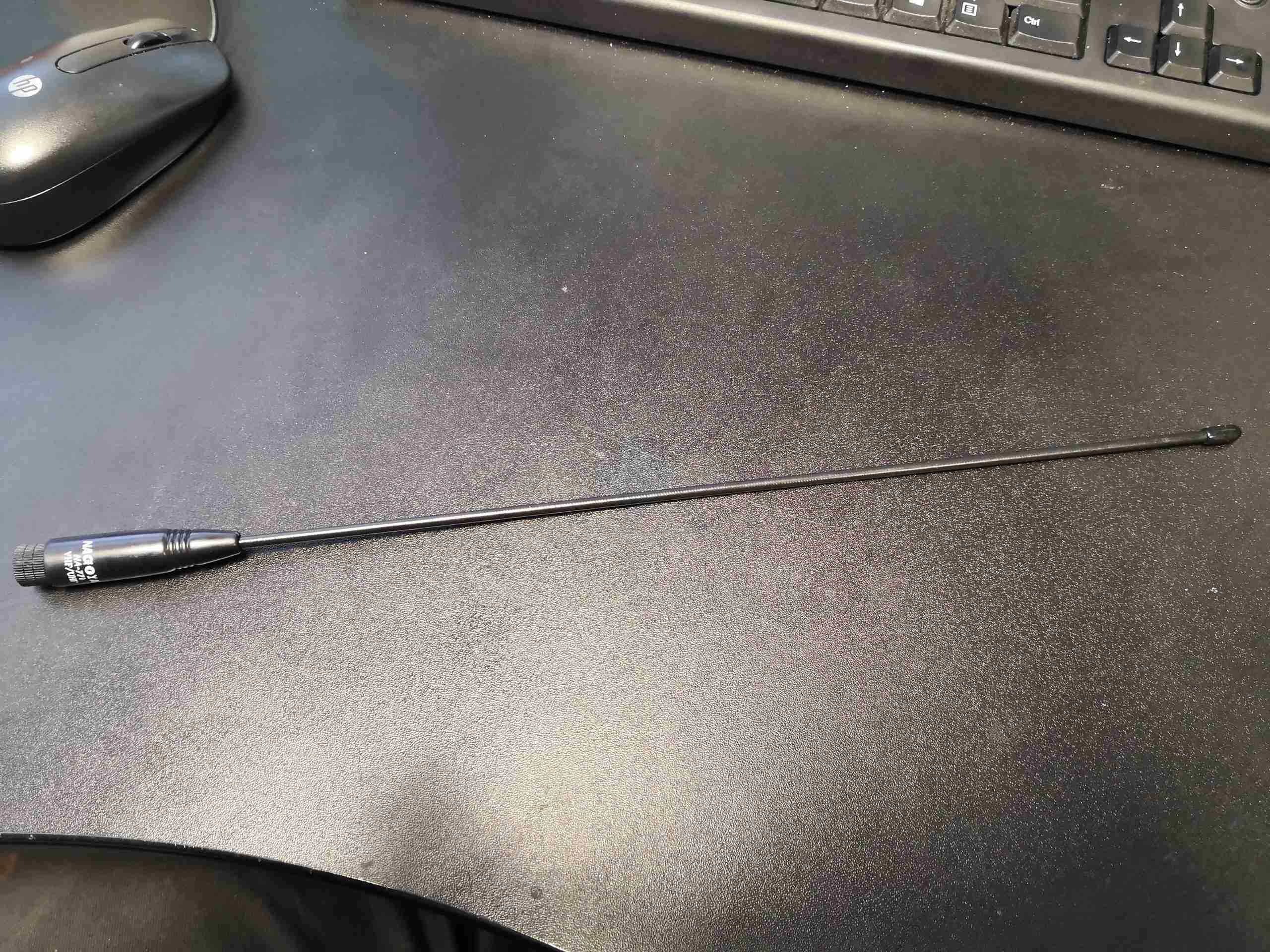
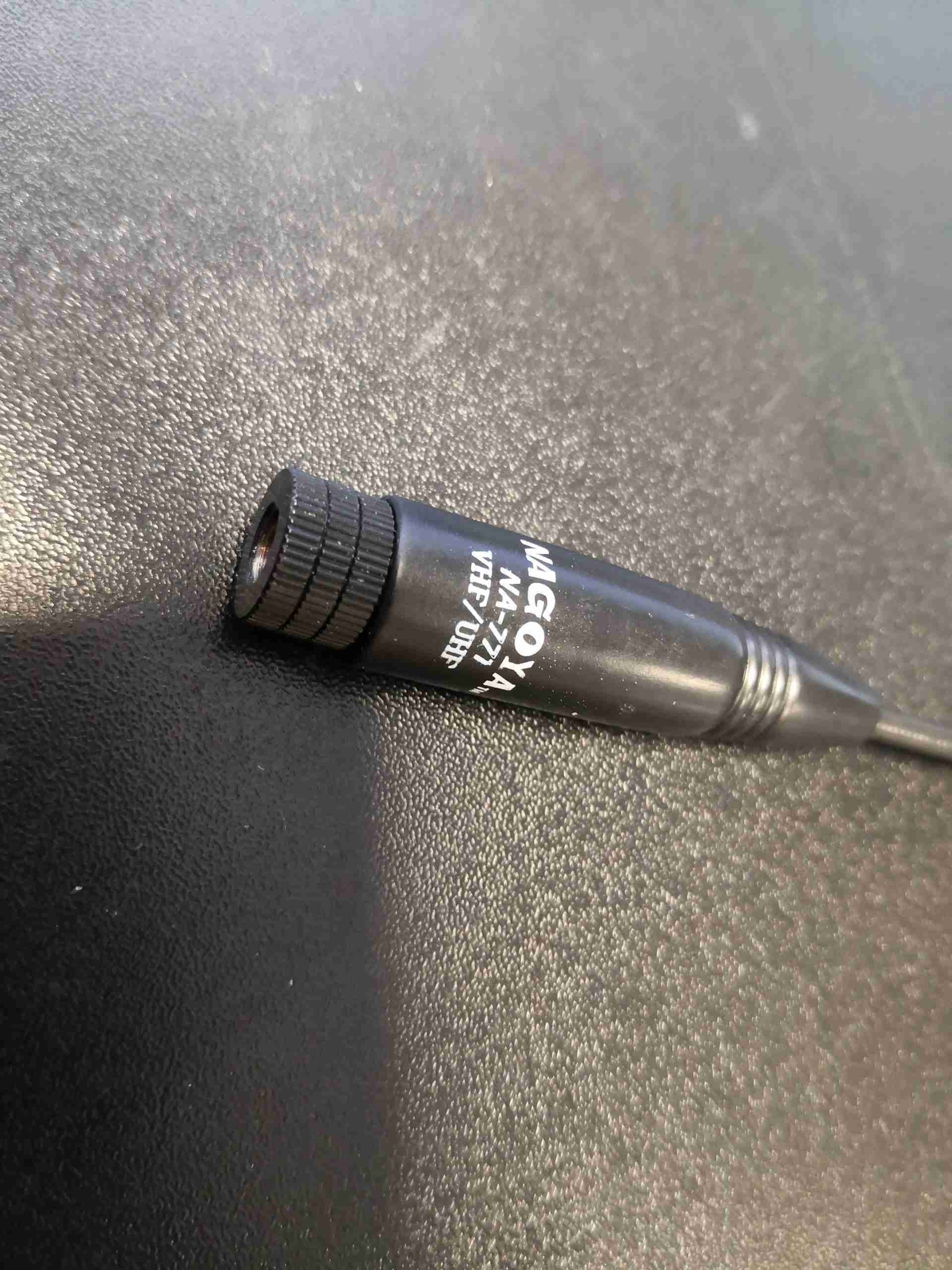
eBay yet again doesn’t disappoint when it comes to fake kit. Here is a claimed dual-band antenna, a Nagoya NA-771. This is supposed to be good for both 144MHz & 433MHz.
Base Logo
The first clue is in the logo printing on the base, it’s not straight, or even. The base isn’t aligned correctly with the connector either, being glued on at a janky angle.
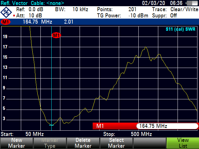
165MHz433MHz
Beyond looks, a network analyser really shows the problems. Here’s a scan from 50MHz to 500MHz. There’s a fairly decent SWR of 2.01:1 at 164MHz (the tuning is still off, it’s supposed to be at 144MHz), but the SWR at 433MHz is 13:1!
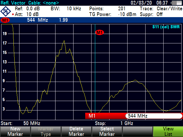
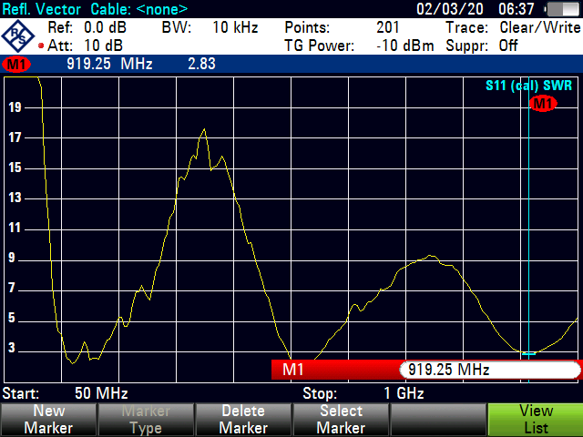
544MHz920MHz
Extending the range to 1GHz does show another couple of resonant points, at 544MHz (1.99:1) & 920MHz (2.83:1), well outside the band that this antenna is supposed to work to.
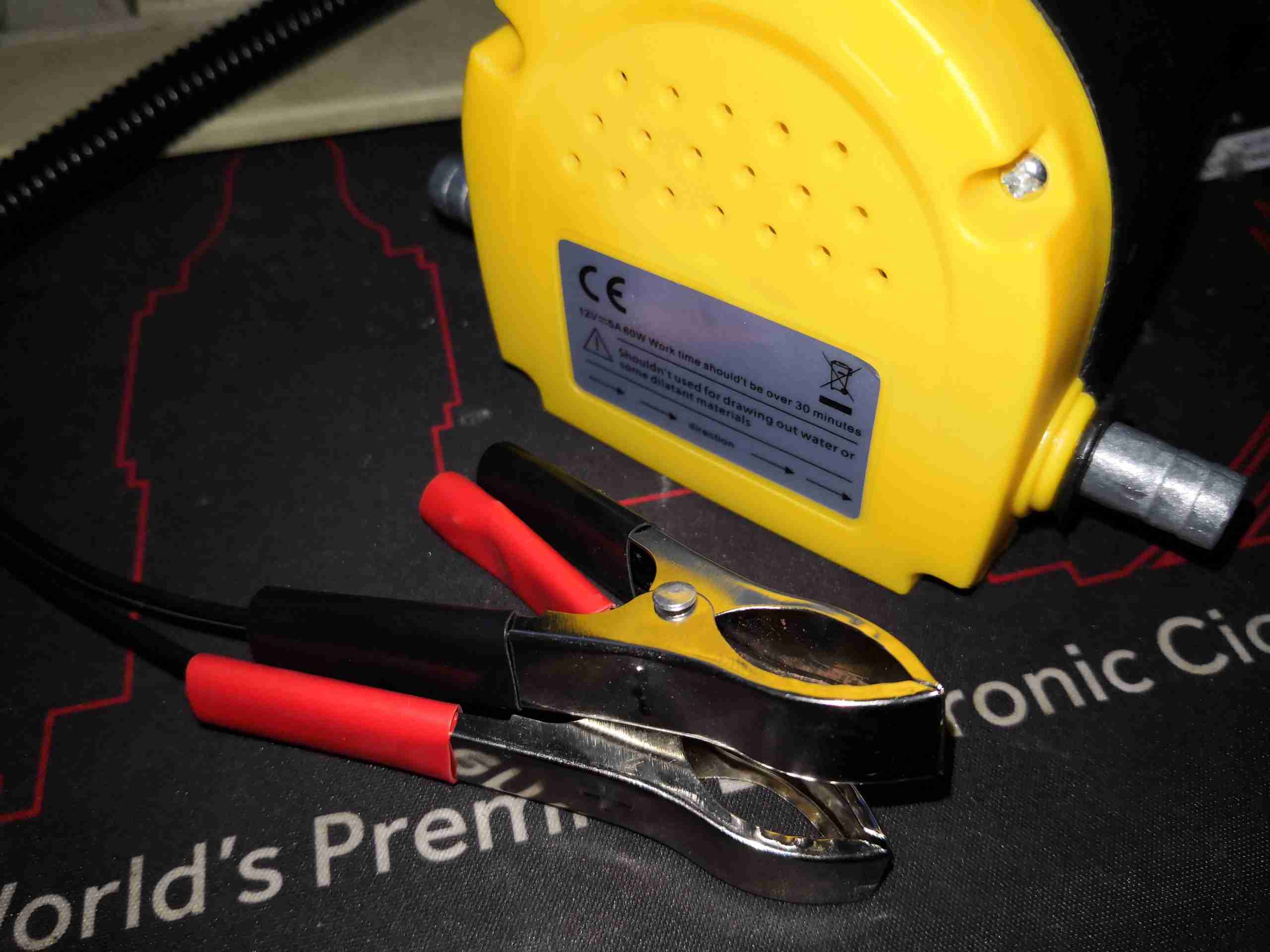
Yet another wonder of Chinese mass-production, this is a cheap (£10 shipped) oil/fuel transfer pump from eBay. Primarily intended for removing oil from engines through the dipstick tube, these are usually sold for all kinds of pumping uses. As will become clear, pumping highly flammable liquids with these might just be a bad plan. Power is supplied through a pair of croc clips, from a 12v battery. Power consumption is quoted at 5A, with a max runtime of 30 minutes.
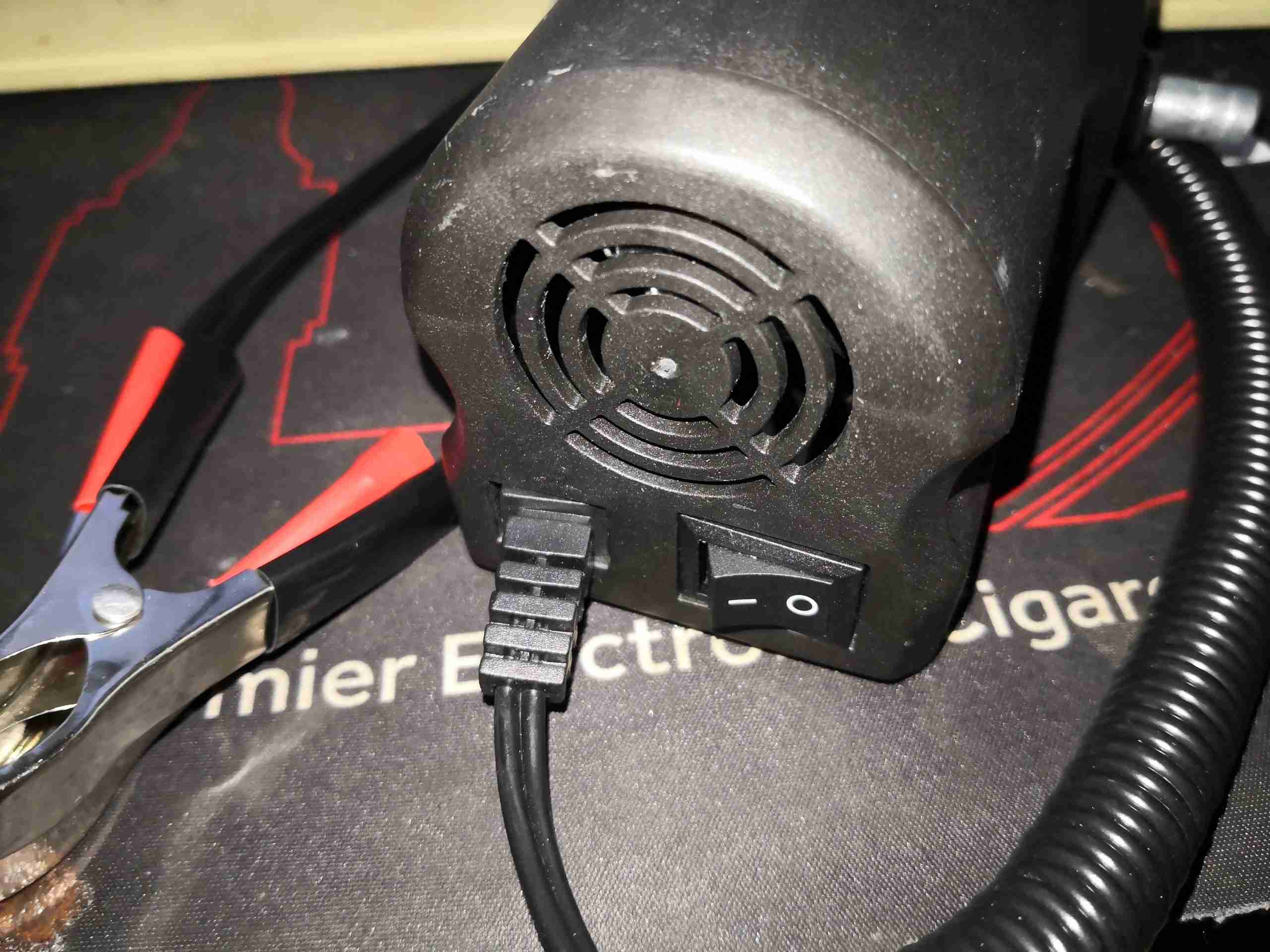
Power Switch
The coiled cable runs into the back of the plastic housing, where a power switch is also mounted. There’s some ventilation holes, but nowhere for air to flow in at the other end. Smart.
Pump Assembly
Removing the 4 screws on the front cover allows the pump unit to slide out, this is just held in place by the clamped halves of the housing on the rubber grommets on the pump ports. This is definitely a positive-displacement pump, as would be required to be self-priming.
Gear Reduction
The pump is driven through a gear reduction from the motor.
Motor
The motor itself is a bog-standard brushed type – and the reason why flammable liquids such as Petrol should not be pumped with this unit. It’s not ignition protected by any stretch of the imagination, and my guess is the shaft seal isn’t brilliant. So any combustible vapour around the motor is going to be ignited quickly by the sparking brushes on the commutator.
Vane Pump
Removing the front cover reveals the pump’s innards. It’s a sliding vane pump! The vanes themselves are made from copper-plated steel, the rotor looks to be metal injection moulded from iron or steel. As the housing is a soft alloy – probably Zinc or Aluminium – I would predict that the steel vanes will make relatively short work of the housing, rather rapidly wearing away the inner surface. Only time will tell on this one.
Splined Shaft & Seal
The rotor is only slipped onto the shaft splines, and comes out easily. The shaft itself does have a seal.
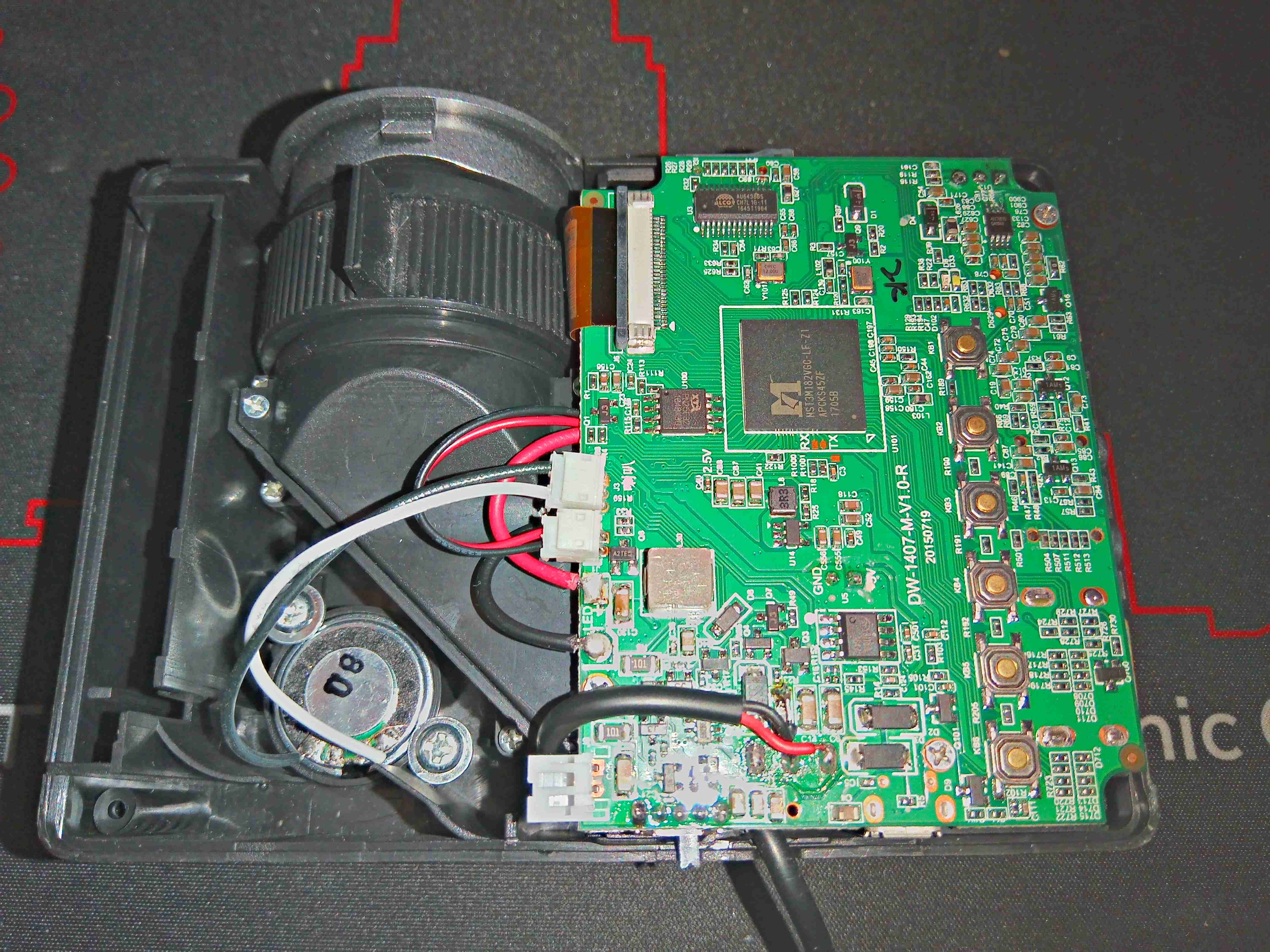
Another Chinese eBay teardown! This is a “720p” LED projector, available from nearly everywhere for very little cash. But they are very little cash for a reason – they’re total shit. The resolution as stated is a blantant lie – the LCD panel used in these is usually around 320×240, nowhere near the 1280×720 as stated. Being small & portable, there’s very little lighting power available, and they barely work to a level watchable without eye strain even in a completely dark room. You literally get what you pay for! Above is the projector with the top removed, showing the main board, which is fairly densely populated.
Mainboard Top
The main processor appears to be an MST3M182VGC-LF-Z1, a SoC designed specifically for LCD TV applications. This runs the internal firmware from a serial flash, a PN25F32 32Mbit (4MB). As this projector has the capability to play files from USB & SD Card, as well as from A/V inputs, there’s an Alcor Micro AU6438BS USB 2.0 Single LUN Flash controller on the right to deal with the MicroSD slot interfacing. The left top corner of the board is completely dedicated to power control, with various switching converters & transistors.
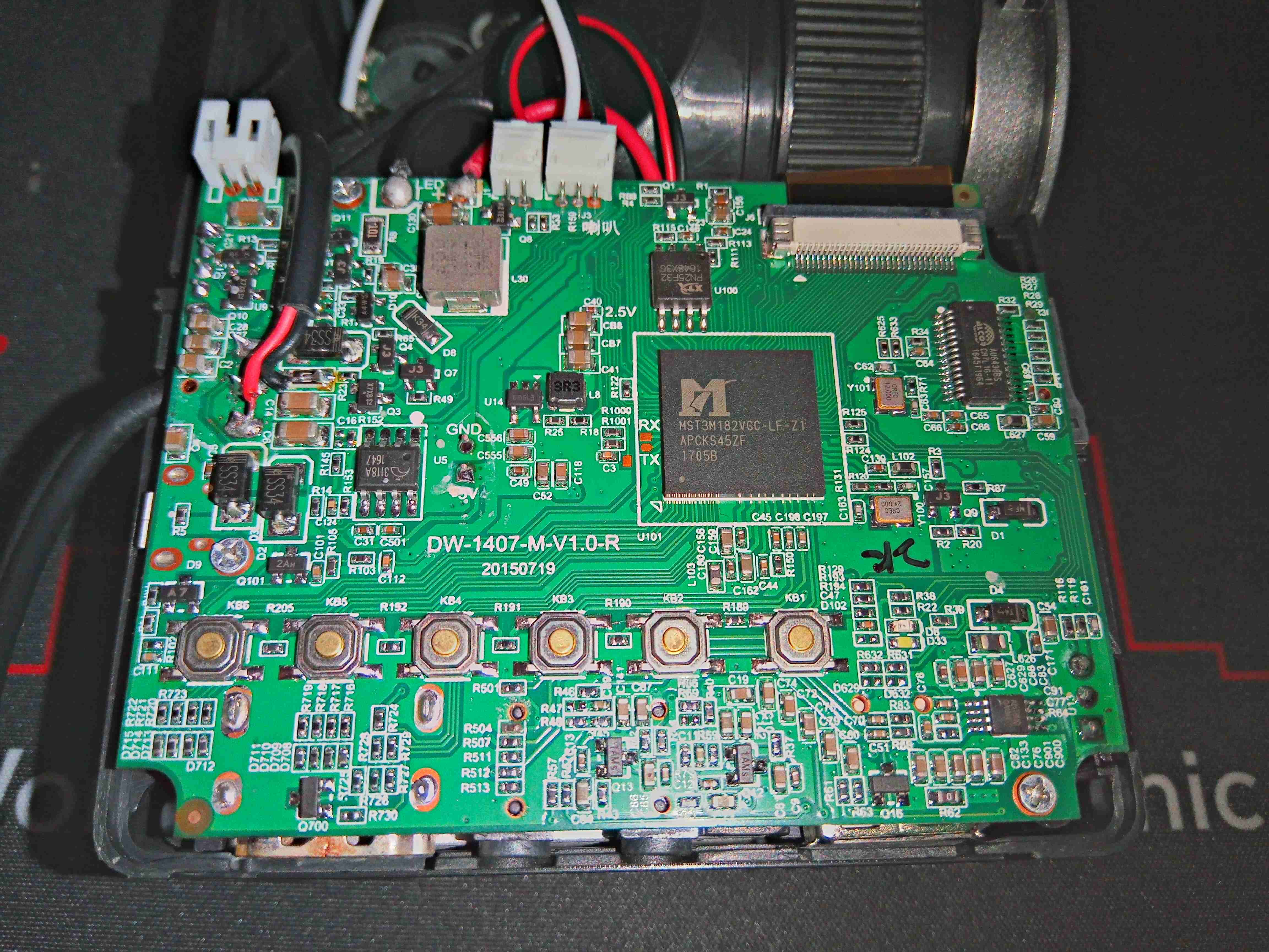
Mainboard Bottom
The bottom of the board is also dedicated to the remaining portion of power control – more switching regulators here generate the voltage rails required for the SoC, along with LED drive.
Optical Path
Removing the board allows access to the optical components of the projector.
LCD & Lenses
Here the LED module has been removed from the casing, better showing the optical arrangement. There’s a Fresnel lens, then a polariser, the LCD panel itself, another lens, then the final turning mirror to the objective lens.
Turning Mirror & Objective
Here the rest of the optical components have been removed, showing the objective with it’s helical focusing track, which moves the lens, and the turning mirror. Behind the mirror is the pitiful speaker.
Optical Components
Here the main components are laid out, with lenses either side of the LCD & polariser.
LED Module
Now onto the light source of the projector – the LED module. This is buried inside the module with a conical reflector, and a small heatsink on the back.
Reflector Removed
Removing the reflector shows the LED itself, with a thermal fuse in series for protection. The LED is screwed to the aluminium heatsink for cooling – my guess is this is roughly a 6W LED, with 3 series pairs of dies in parallel.
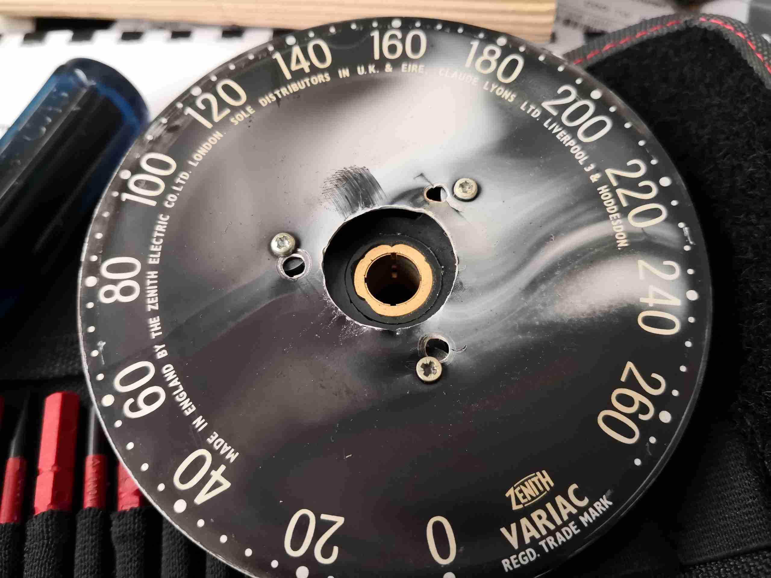
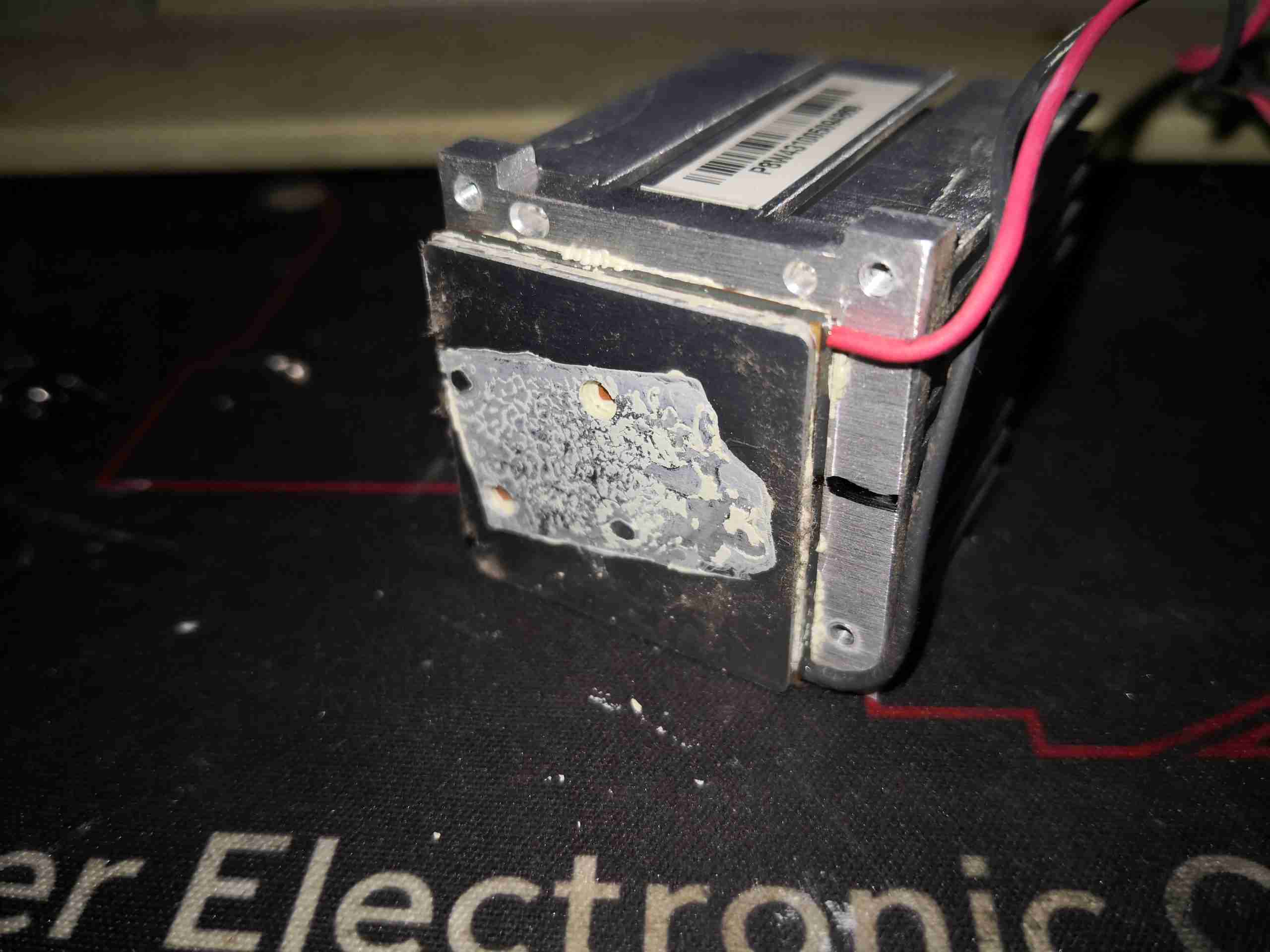
Well, this is what happens when a Variac rated at 3A is subjected to 15A for a while – a complete burnout. The smell associated with this failure was formidable, it’s a shame I can’t convey odour through photos! Above is the burned section of the winding (it was set for around 115v output from our 240v mains).
Top Cover Removed
At first the rotor was stuck in position, but a bit of force allowed some movement. The armature holding the brush has melted at the rivets, and the copper tail from the brush is severely heat-discoloured. This got HOT! When brought to me just after failure, it was near impossible to hold onto the outer casing!
Smoke Residue
Underneath the control knob, there’s white ash, which has evolved from the insulation burning off the windings.
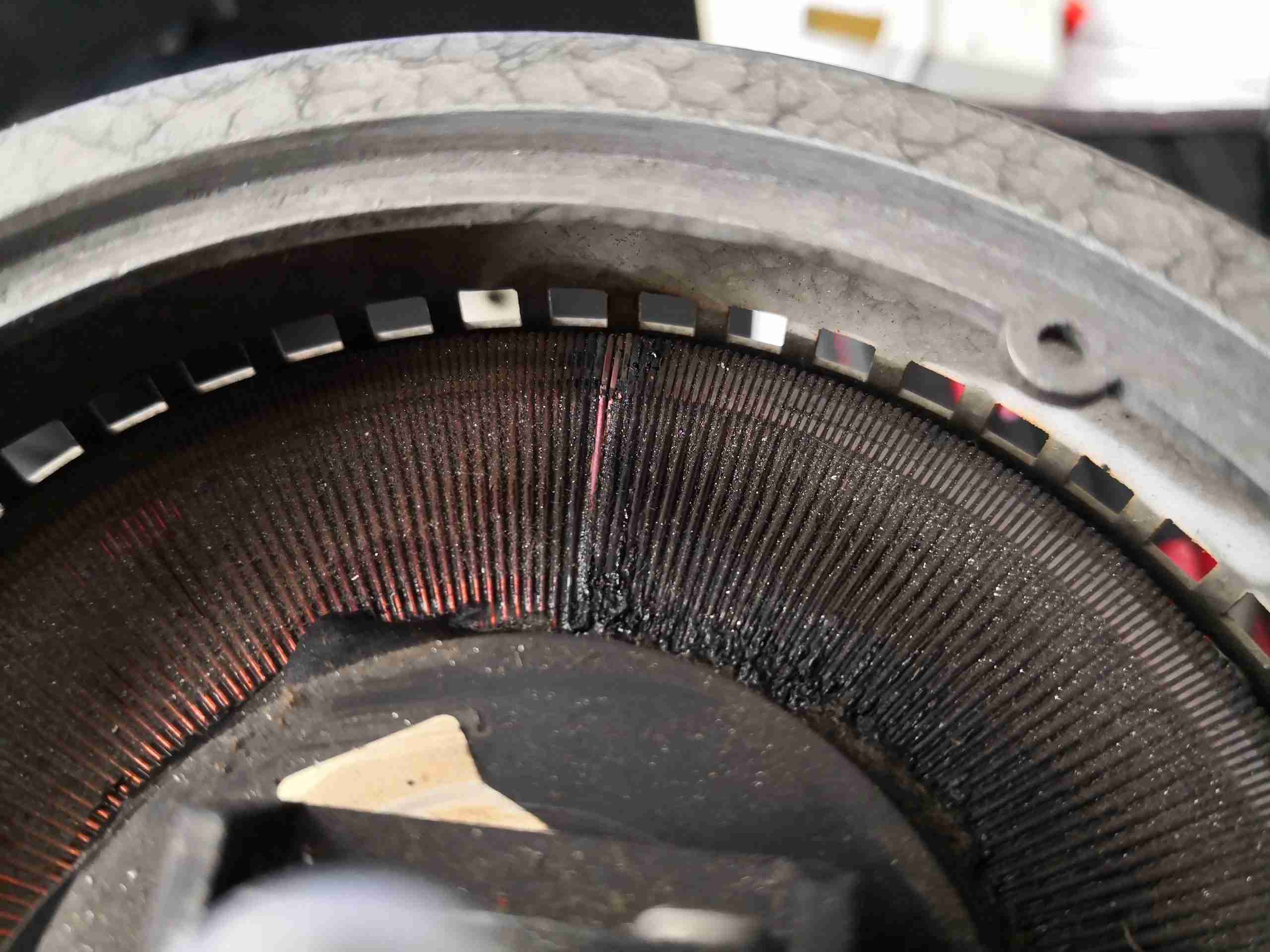
Shorted Turns
A closer look at the point where the brush was set shows the pair of windings have pretty much fused. The worst of the heating occurred here it seems.
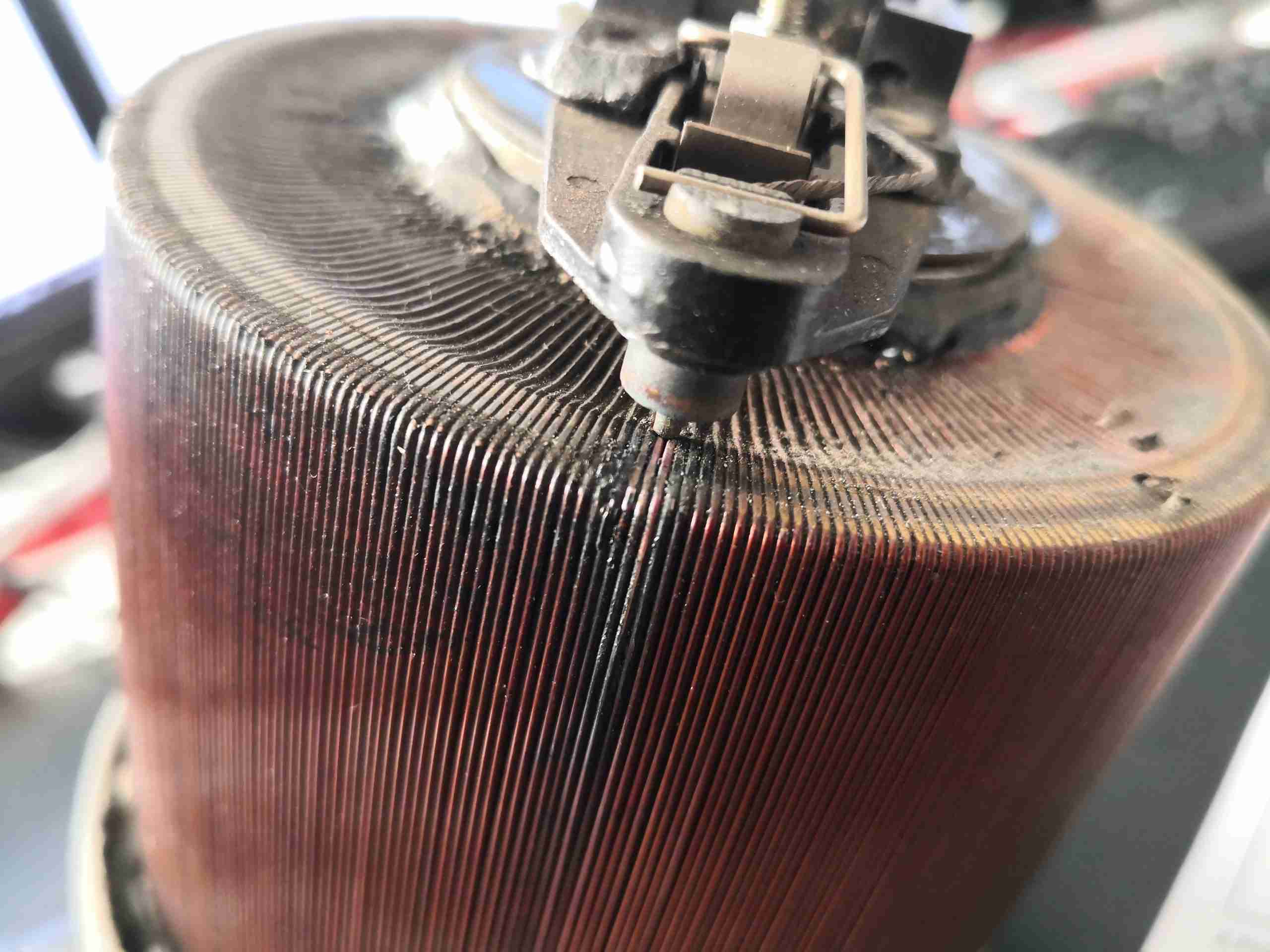
Windings
The heating has extended down the windings and the insulation has melted all around the top & base of the toroid core. Unfortunately it’s the end of the line for this particular transformer, and it now rests in the Black Museum of Electrical Death.
These projectors were very popular when they first appeared on the market with the laser hobbyist community, and for very good reason – they contain a massive array of 445nm Royal Blue laser diodes in their optics engine. Originally very expensive, these units can now be had for under £50 on eBay, usually with damaged DLP chips.
Laser Module Door
Under the door on the bottom of the projector is the 445nm Laser diode array module, itself secured in place with security screws to the beam combiner. The rack of 3 high speed fans to the left draws air over the substantial heatsink.
Top Cover Removed
After removing the shell securing screws, the top cover comes off with the button panel. This gives a view of the internals, mostly PCBs at this stage.
Main Control Board
On the left side of the projector is the main control PCB, with the video handling circuitry.
DLP Chipset
At the top of the board is the main DLP image processing chipset, these two components are actually custom parts, so no datasheets are available. The main DLP IC has some DRAM & a Spansion serial flash for firmware storage. There’s also a small audio amplifier on the left to drive the onboard 2W speaker.
System Microcontroller
Further down the board sees an unpopulated BGA footprint, with more space for DRAM. The main system microcontroller is on the right, a Renesas part.
Phosphor Wheel Motor
Right at the bottom edge is the connector running off to the phosphor wheel drive motor.
DC-DC Power Management
The reverse side of the board is pretty sparse, there’s quite a few passives & power control. Down towards the bottom surrounded by inductors is the system power management IC, the DLPA100. This takes the incoming DC 12v rail from the connector on the right side of the board & produces several supply rails for the internal logic: 1.1v 1.8v, 2.5v, 3.3, 5v & also contains the 3-phase brushless driver for the phosphor wheel motor. The main control board input power connector also has a +5v from the mains supply, for standby power. The main board signals the PSU to switch on the main +12v rail through a pin on this connector.
HDMI Interface Chipset
The other end of the board just has the connectors, a bit of glue logic & the HDMI interface chipset.
Main Board Removed
After unplugging all the connectors, the massive cast frame of the light engine is visible.
Phosphor Stripe
Here’s a closeup of the phosphor stripe around the edge of the wheel. This takes the 445nm light from the laser module, and converts it into green. There’s also a frosted glass section of the wheel to pass some blue for the image. The reason for the phosphor being in a large stripe on the wheel is load spreading – there’s several watts of optical power focused down to a very small spot on this phosphor, and would overheat quickly if it wasn’t moving.
DLP Frame
At the back of the light engine is the DLP module, with it’s substantial heatsink.
Light Source PSU Board
Hiding under the mains PSU, is the light source control PCB. This contains several DC-DC converters, which run the 4 strings of laser diodes, the large Phlatlight Red LED & it’s associated TEC cooler. This board takes the incoming +12v from the mains PSU through the multi-way loom at top centre. There are multiple cores on this connector to spread the load – at normal brightness, in Eco mode, I measured the power consumption at about 8.5A at 12v input for the entire projector.
DC-DC Converters
The left side of the board is dedicated to the high power section of the controller. There’s a power inductor for every channel.
Light Source Drive Board
The other side of the board is very heavily populated with components.
Control Logic
The right hand side has the control logic, a Lattice CPLD, and another Renesas Microcontroller. There’s also some glue logic here & a dedicated DA converter.
Power Drivers
The other end of the board has the power drive control logic. There’s a MAX16821AA LED buck driver for the Red LED, and 4 drive ICs for the laser diodes, which are marked <009 LDGC N249. I haven’t been able to find anything about these, so they may be custom.
DLP Light Engine
Removing some screws allows the entire optical assembly to be removed from the lower shell. This may be mostly manufactured from a magnesium alloy from the rather low weight.
DLP Board
On the back of the DLP module is the DLPA200 Micromirror Driver IC. This generates the high voltage bias supplies for the DMD chip (+/-28v) from the 12v rail, generates all the timing waveforms required for the DLP chip. There’s a couple of power inductors for the onboard regulators. Video data is sent from the main image processing chipset to the DMD chip via 2 channels of LVDS.
DLP Mount
Now the heatsink has been removed, the rear of the DLP chip can be seen, with the remains of the thermal pad. The mount for the heatsink is sprung, to accommodate thermal expansion.
Red PhlatLight
The Red light required to create a colour image is generated by a giant LED, more on this one later.
DLP Removed
Here’s the DLP board removed from the projector with the micromirror surface visible. This DLP has many dead pixels, hence the decommission at ~4500 hours of operation.
Laser Beam Combiner
The 24 laser diodes have their beams combined by this knife-edge mirror assembly, turning the beam through 90° to the lens on the left, which focuses the 24 beams down to the optics engine.
445nm Laser Array
Removing the beam combiner from the array allows the 24 diodes to be seen, mounted under their collimating lenses. This is one beast of a laser unit!
Dichroic Optics
Taking the cover off the optics assembly allows the main optical path to be seen. The blue laser comes in a bottom left, through the lens, the red LED comes in bottom right. The pair of dichroic mirrors manage the light path for the red & green light, while passing the blue straight through.
Optical Path
Here’s another view of the optical path, with both light sources visible.
Light Homogenizer
After the light source, is the homogeniser – this tunnel of 4 mirrors facing each other evens out the light beam & removes all coherence from the laser light. This is important to not have any speckle in the image.
Focus & Zoom Motors
Underneath the objective lens are the pair of stepper motors that drive the focus & zoom mechanisms, along with their position sensors.
Turning Mirror
Just after the homogeniser, is the final optical path to the DLP. Here the light comes in a bottom left, and hits the turning mirror, after which it is focused onto the DLP chip by the mirror top centre. The objective lens is through the hole in the centre of the optical block, while the DLP is on the right side.
DLP Final Optics
Here’s where the DLP will be mounted in normal operation, with it’s lens in place.
Objective Lens
Finally, the created image is passed out through the objective lens to the projection screen.
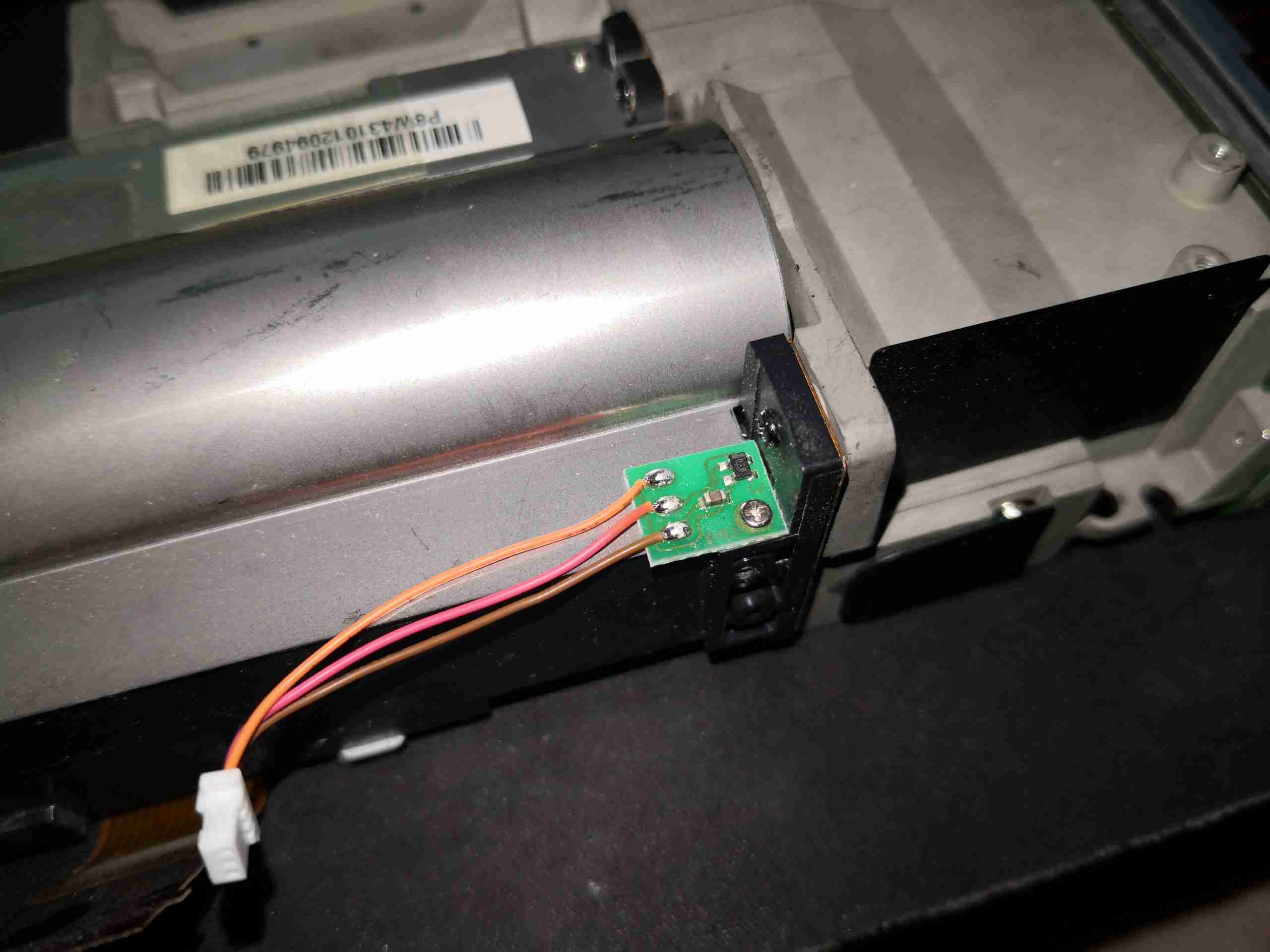
Hall Effect Sensor
There’s a sensor mounted on the side of the lens barrel, that I think is a Hall effect device, but I’m unsure what this would be used for, as there is no magnet anywhere near this to sense. It could also be a temperature sensor though, for the DLP & lens assembly.
Stepper Motor Drive
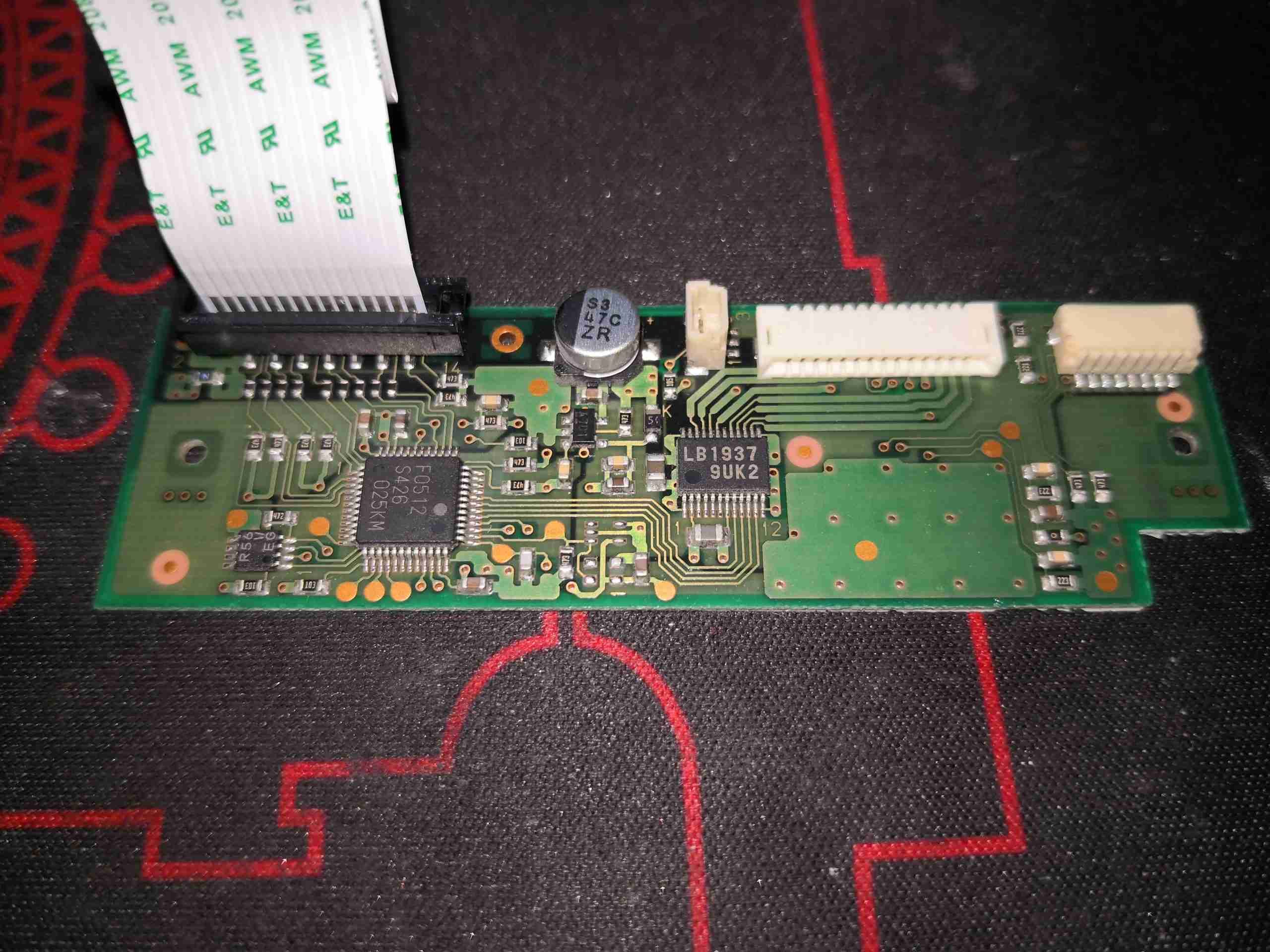
The small PCB on the side of the lens unit holds the stepper motor drive IC, an LB1937 from Sanyo. There is another IC here, which looks to be a microcontroller.
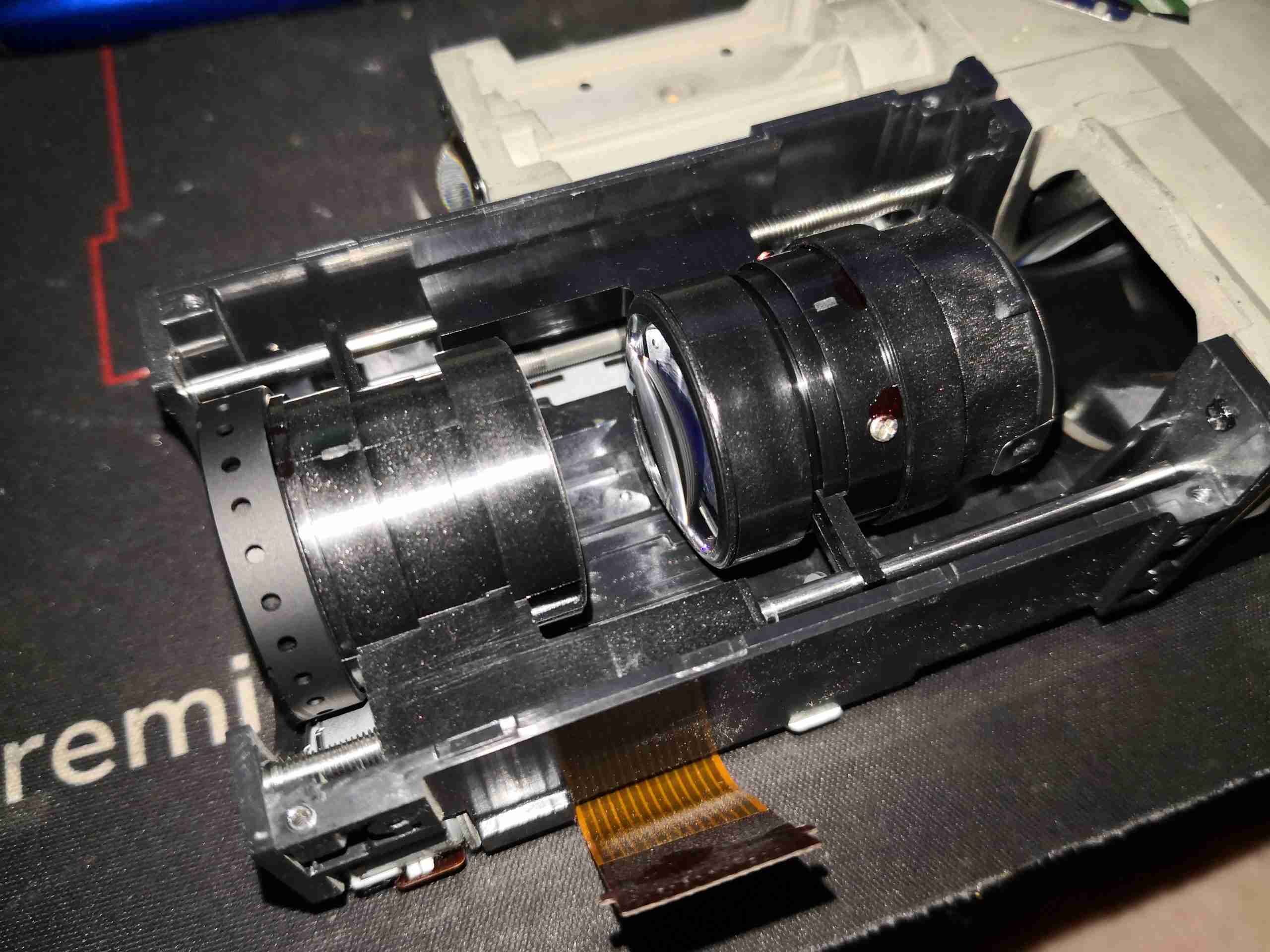
Lens Assembly
Removing the top cover allows the moving lens assemblies to be seen. These move independently of each other to implement focus & zoom, via lead screw drives on the stepper motors.
Blue Light Path
Here I’m shining a separate 445nm diode laser into the optical assembly, through the blue optical path. The phosphor wheel is turned to the clear section, which allows the 445nm light to pass straight through, being turned 180° by the mirrors & directed out towards where the DLP assembly would be.
Green Light Path
Turning the phosphor into the light path causes a very bright green light to be generated, and passed back towards the 445nm laser entry point. The dichroic mirror in the way reflects this light to the left, through a lens & then to the other dichroic mirror to be turned another 90° to the DLP assembly. I’m not sure where the magenta light is coming from – the phosphor probably generates light on more wavelengths than just pur green, giving some red to mix with the blue.
PhlatLight LED
Here’s the Red LED removed from it’s cooling & collimation assembly – this has an enormous silicon emitter area, and apparently these LEDs are designed to be uniform in light emission, specially made for projection use. There’s a thermistor onboard for temperature sensing – sensible when the datasheet gives CW currents of 8A, and pulsed currents of 13.5A!
LED TEC Cooler
Not surprisingly, cooling this beast of an LED requires more than just a heatsink, so it’s mounted on a TEC module, possibly around 40W thermal capacity.
Fan Control Board
Fan control is handled by this little PCB, squeezed in between the optics engine & 445nm Laser array. There’s a SMSC EMC2305 I²C 5-channel PWM fan controller on here, communicating back to the main system microcontroller. Besides some passives, and 4 transistors to make sure the fans don’t start at full power when the projector is powered on, there’s not much else.
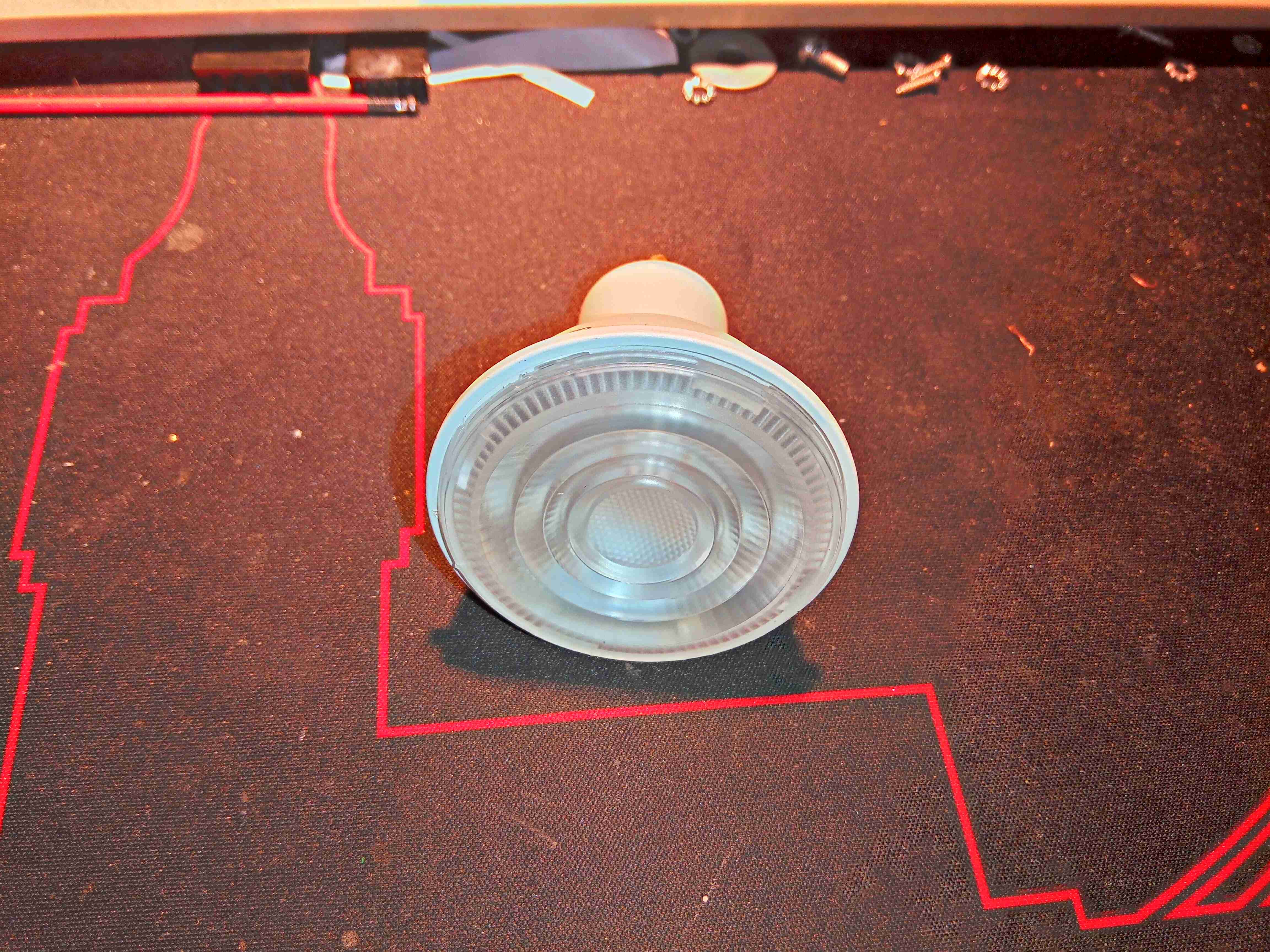
Here’s a recently failed 5W GU10 lamp, which is completely dead – not even a single LED still shining.
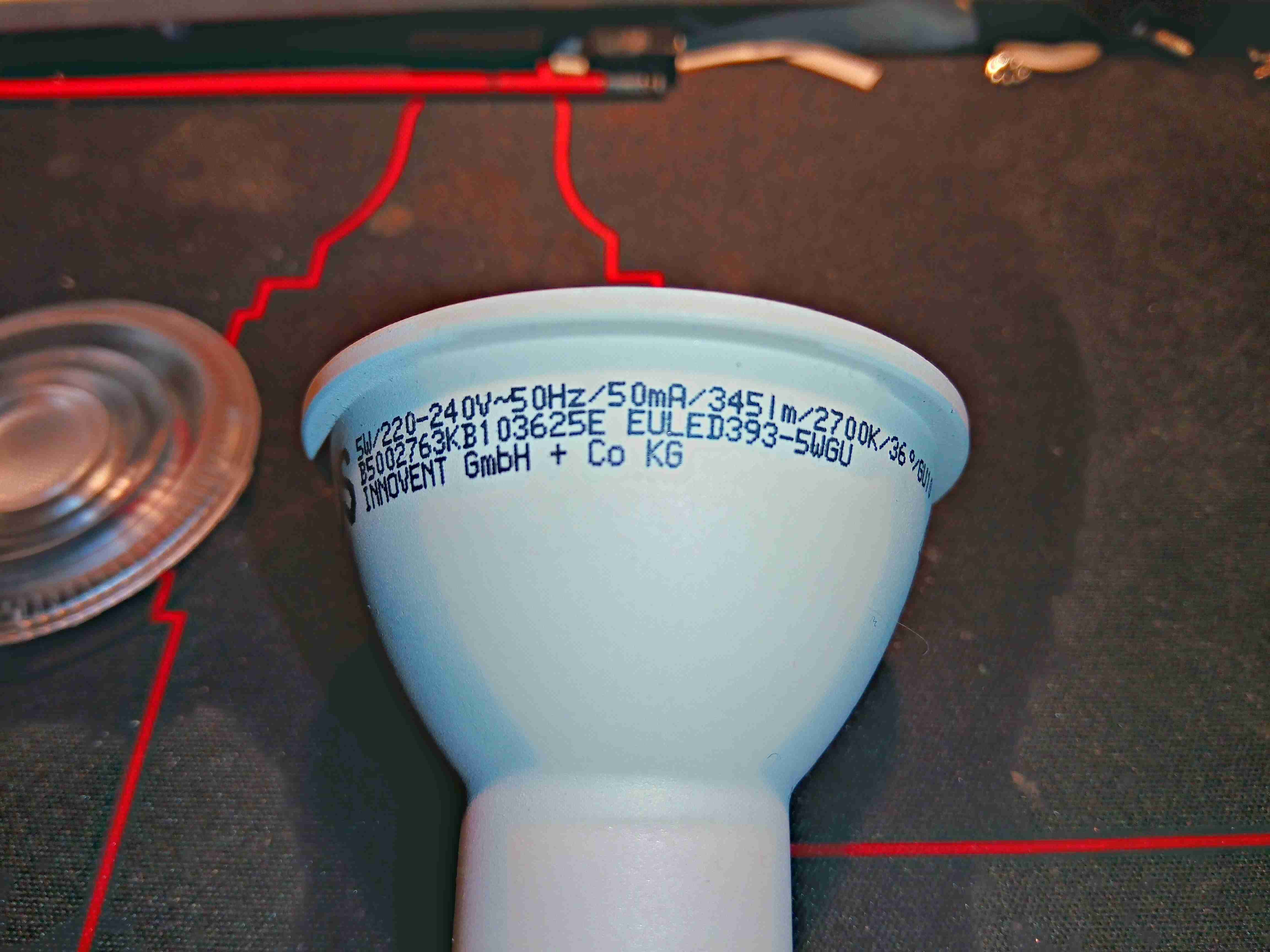
Markings
According to the markings, this lamp draws 50mA at 230v & outputs 345 lumens
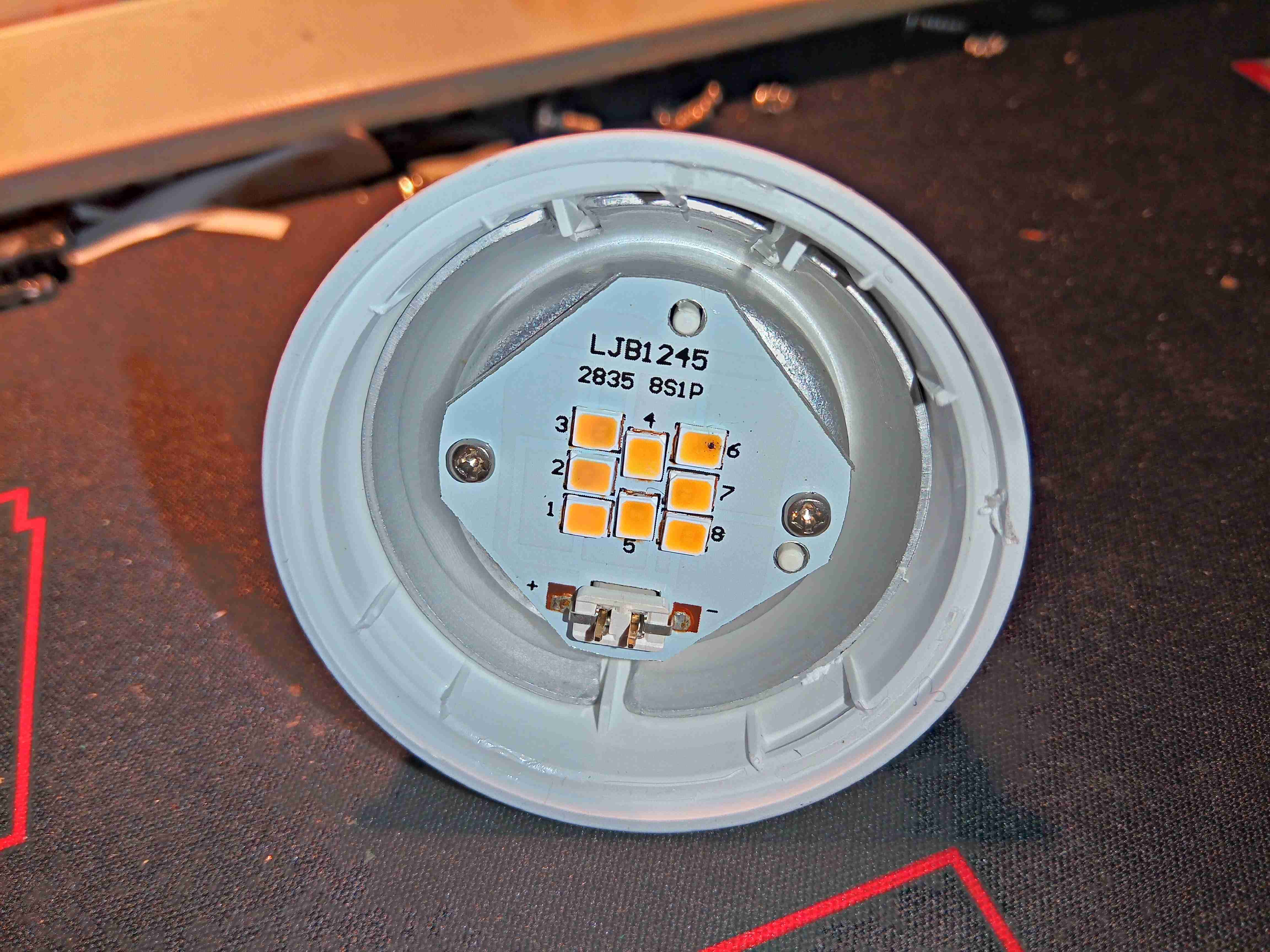
Lens Removed
After popping the lens off the body, the failure mode is obvious. The top right LED has the Black Spot Of Death, where one of the LED dies has catastrophically failed in service. As these lamps usually have all the multi-die LEDs in series, a single failure will cause the lamp to totally fail. Running LEDs hard, with little cooling is a common cause of this kind of failure. There isn’t much in the way of heatsinking in this lamp, as the outer casing is plastic, and even though the LEDs are soldered to an aluminium cored PCB, the only other heatsink is the aluminium base for the PCB, which is in contact with the outer plastic.
PSU
Removing the LED board & backing plate allows access to the power supply in the rear of the lamp. There’s no switching supply in this one, just a large film capacitor.
Capacitive Dropper
Snipping the pins off the back allows the PCB to be removed, exposing the capacitive dropper from the mains. The output electrolytic cap has also failed on this board, as can be seen from the opened vent on the top.
PCB Reverse
There isn’t much on the back side of the board, apart from the bridge rectifier & a couple of resistors.
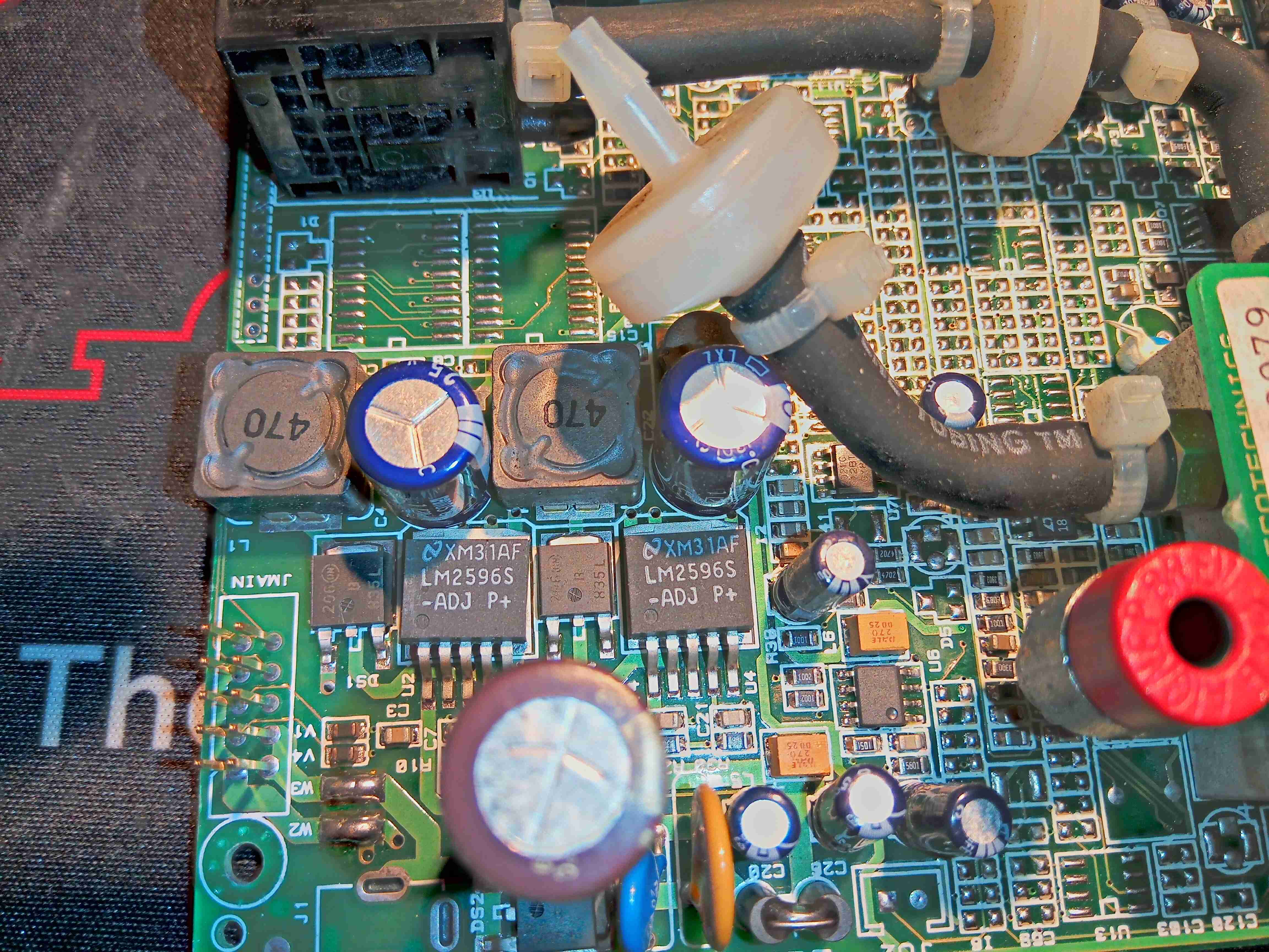
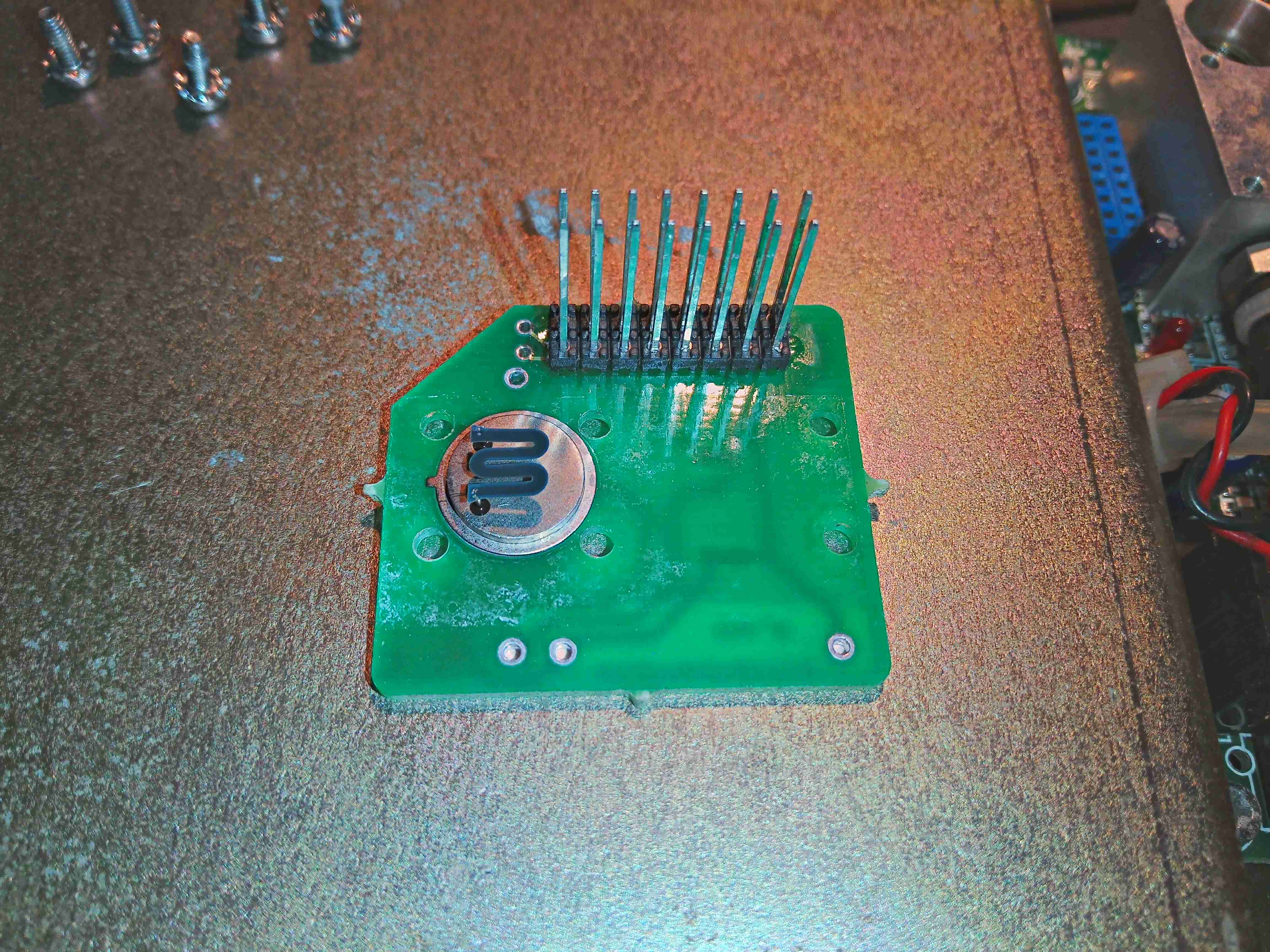
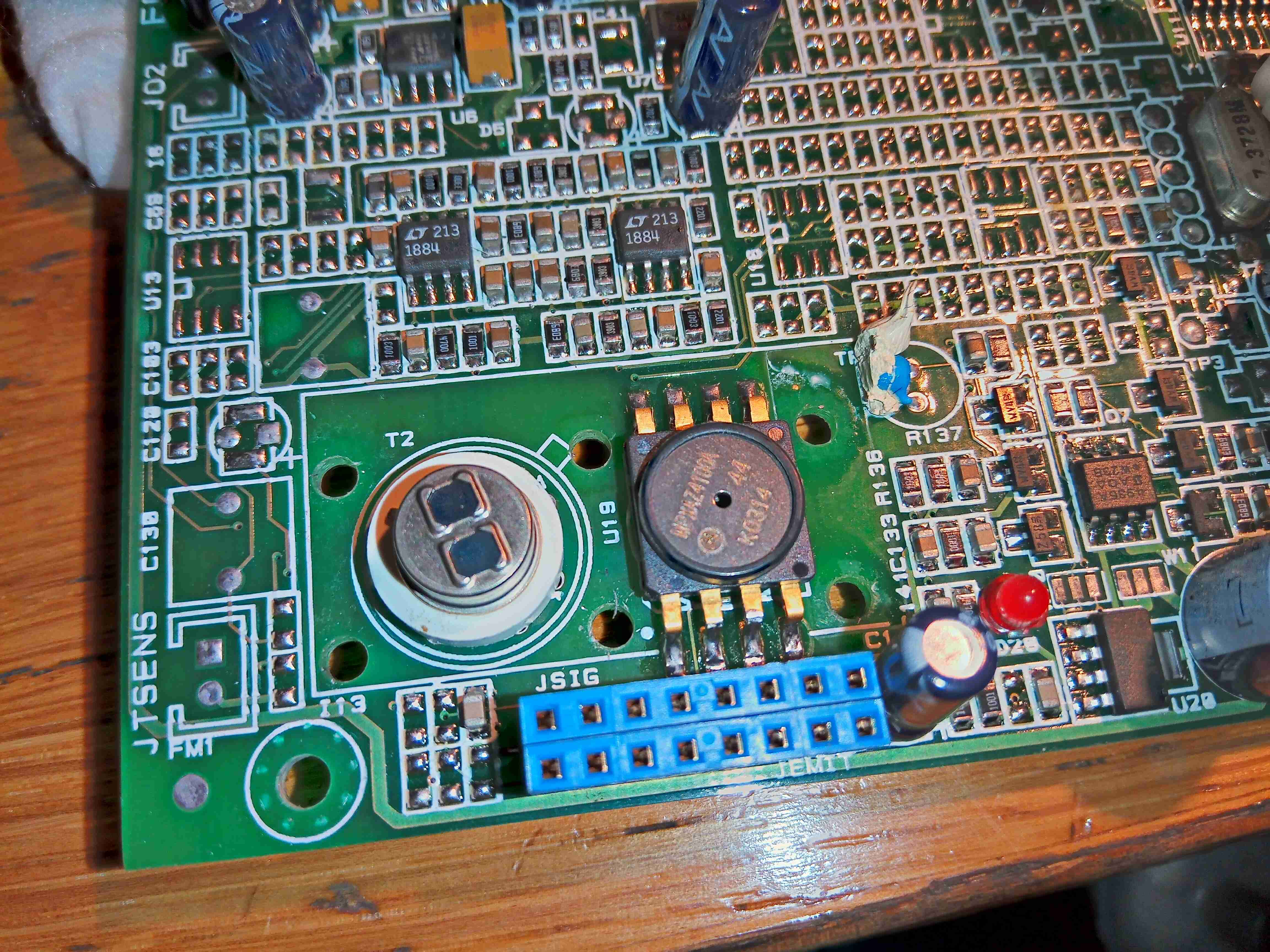
This unit recently appeared on eBay, as a spare part from a refrigerant charging machine, and I figured it would make a good explorational post. This unit analyses the purity of R-134a refrigerant gas, using an Infrared sensor cell, and communicates over RS-232.
The sensor cell itself is at the top right of the board, we’ll get to that later on. There’s a small diaphragm pump at the lower right, for purging the cell with air. The port with the red cap is the outlet, and the remaining open hose barb is the input of gas to be tested. This would connect to a flow regulator & solenoid valve that the board controls.
It’s pretty clear that this board has multiple applications from all the unpopulated components. There’s space for a keypad, indicator LEDs & an LCD on board, so maybe this can also be fitted to a handheld analyser?
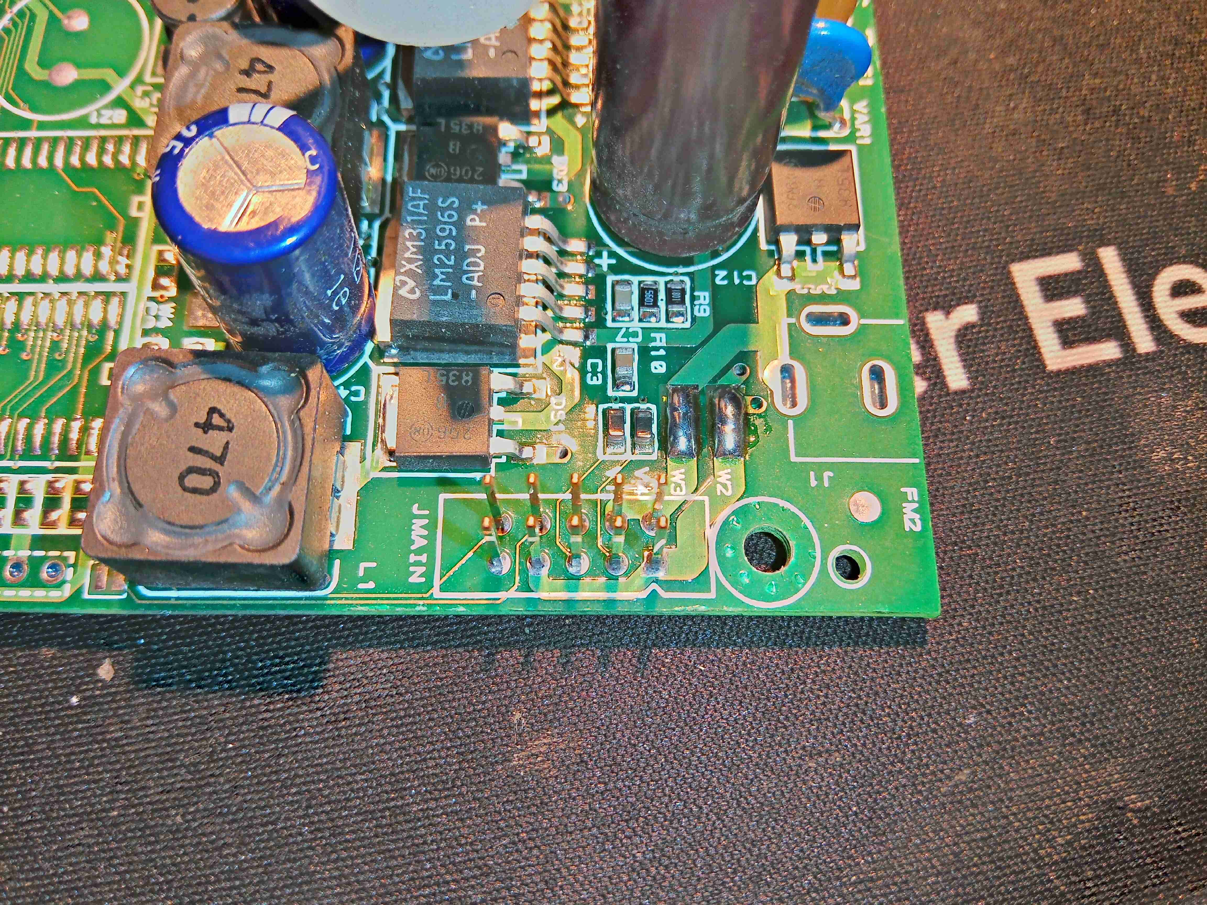
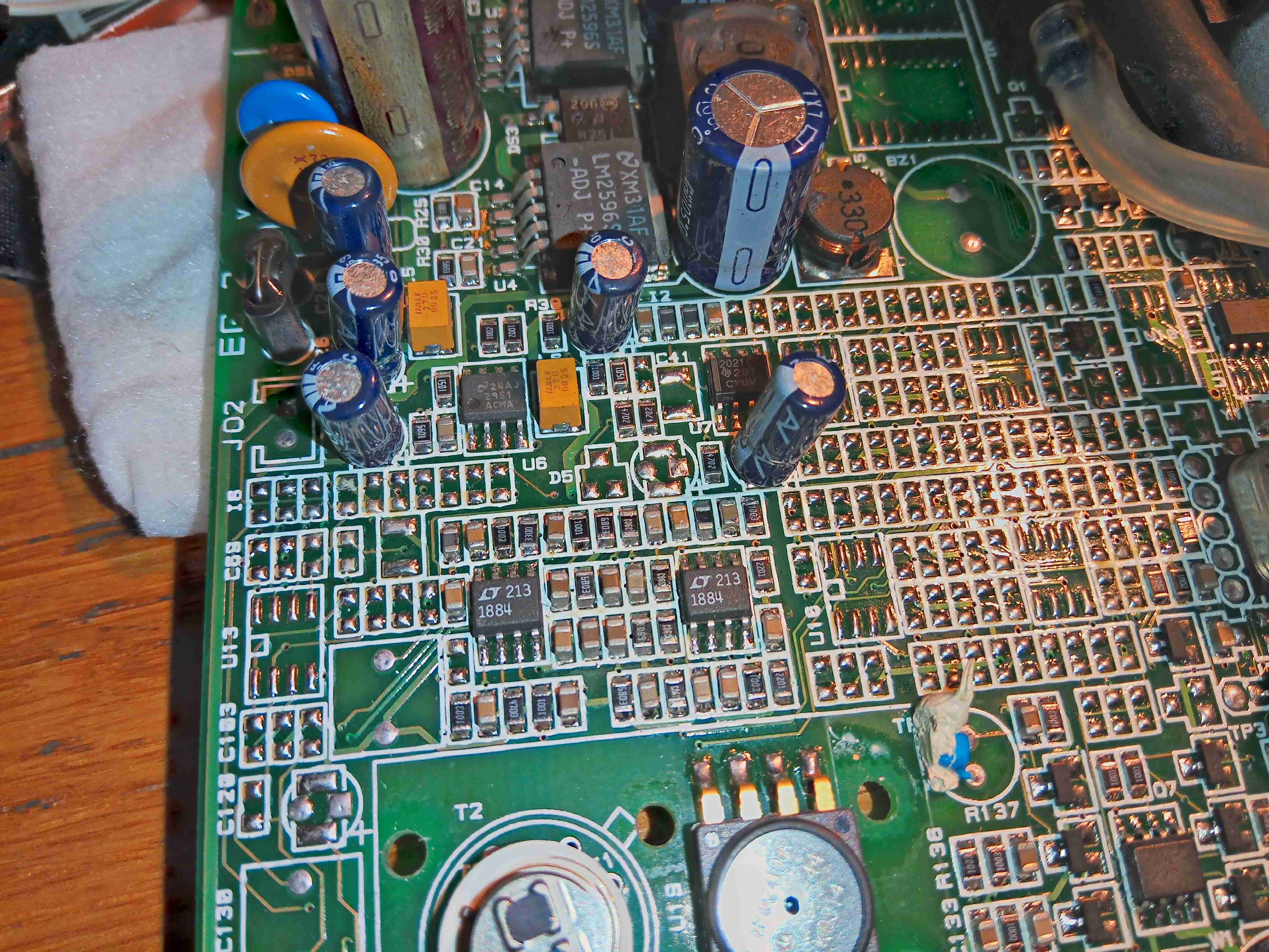
Power Supply
From looking at the input circuitry, I can surmise that the input voltage is somewhere between 12-24v DC, as there is a 35v input electrolytic filter capacitor. There’s a couple of switching regulators which generate 5v & 3.3v rails for the board, with some input fusing.
Main Connector
There’s two serial links on this board, driven from the main microcontroller – the primary one is on the connector marked JMAIN, along with the power input & a couple of other unknown signals.
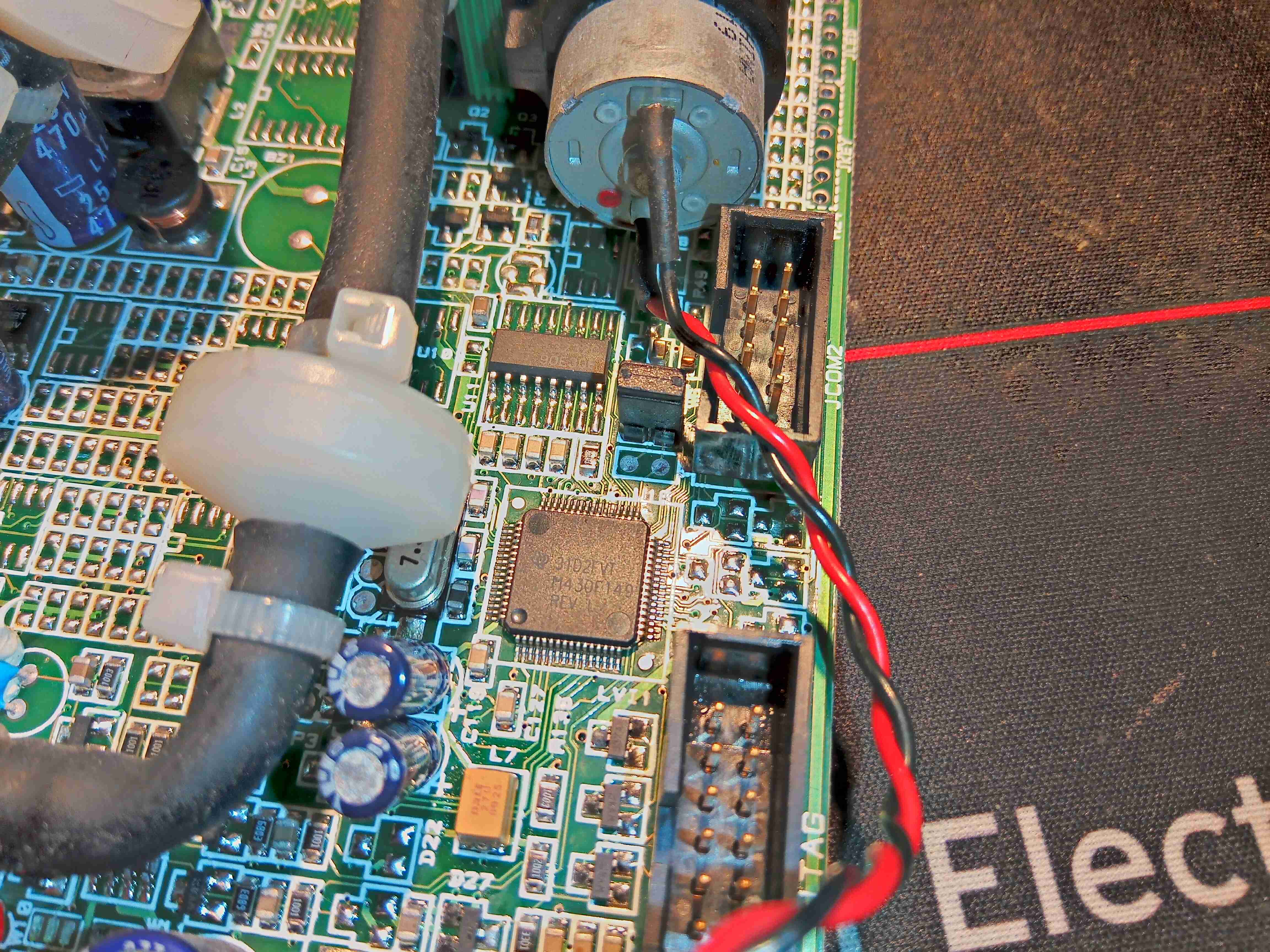
MSP430 Microcontroller
Over on the other side of the board is the brains of the operation – an MSP430 microcontroller, with an RS232 transceiver IC & another RS-232 port marked COM2. The remaining connector is a JTAG port for the micro.
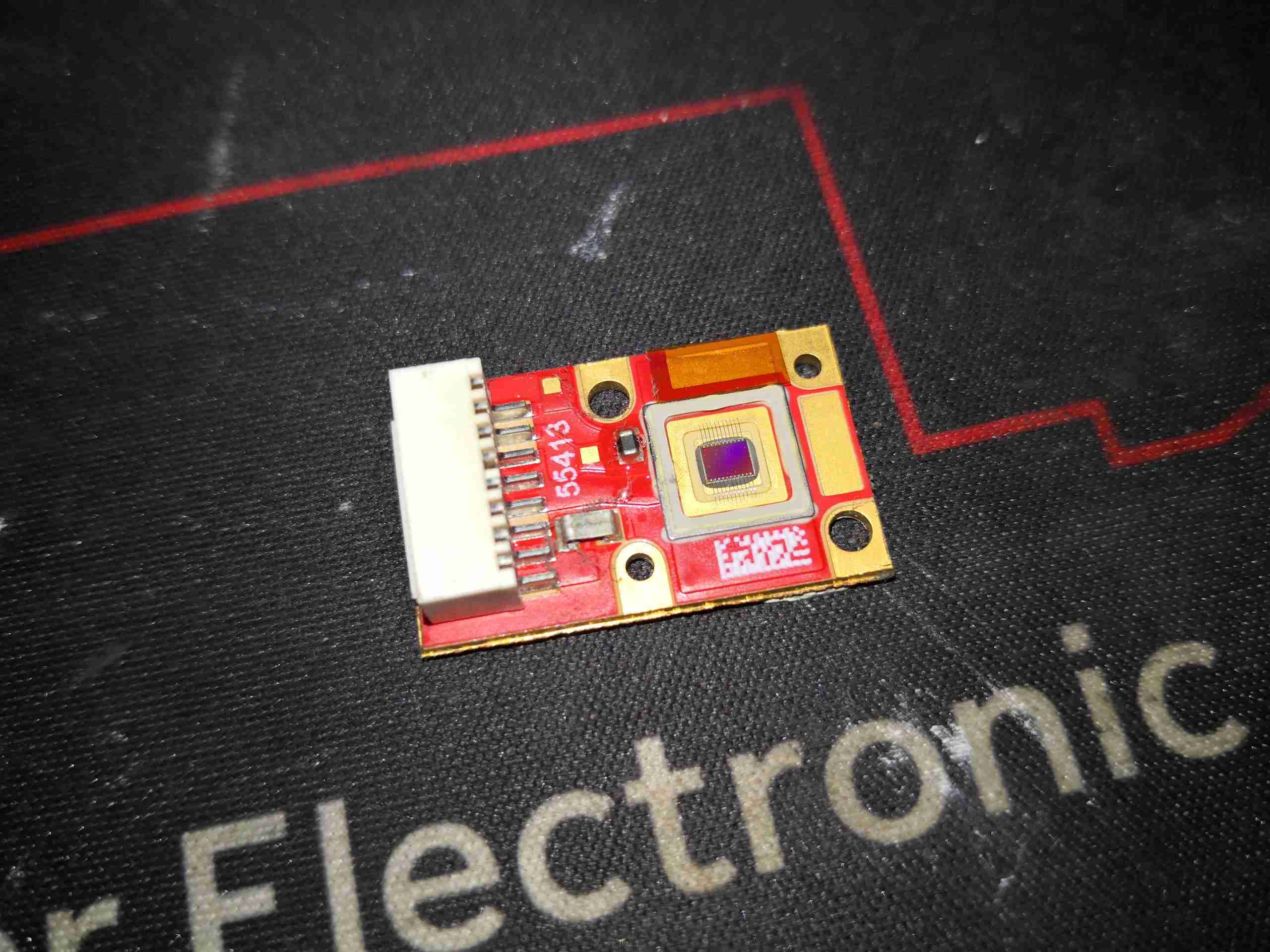
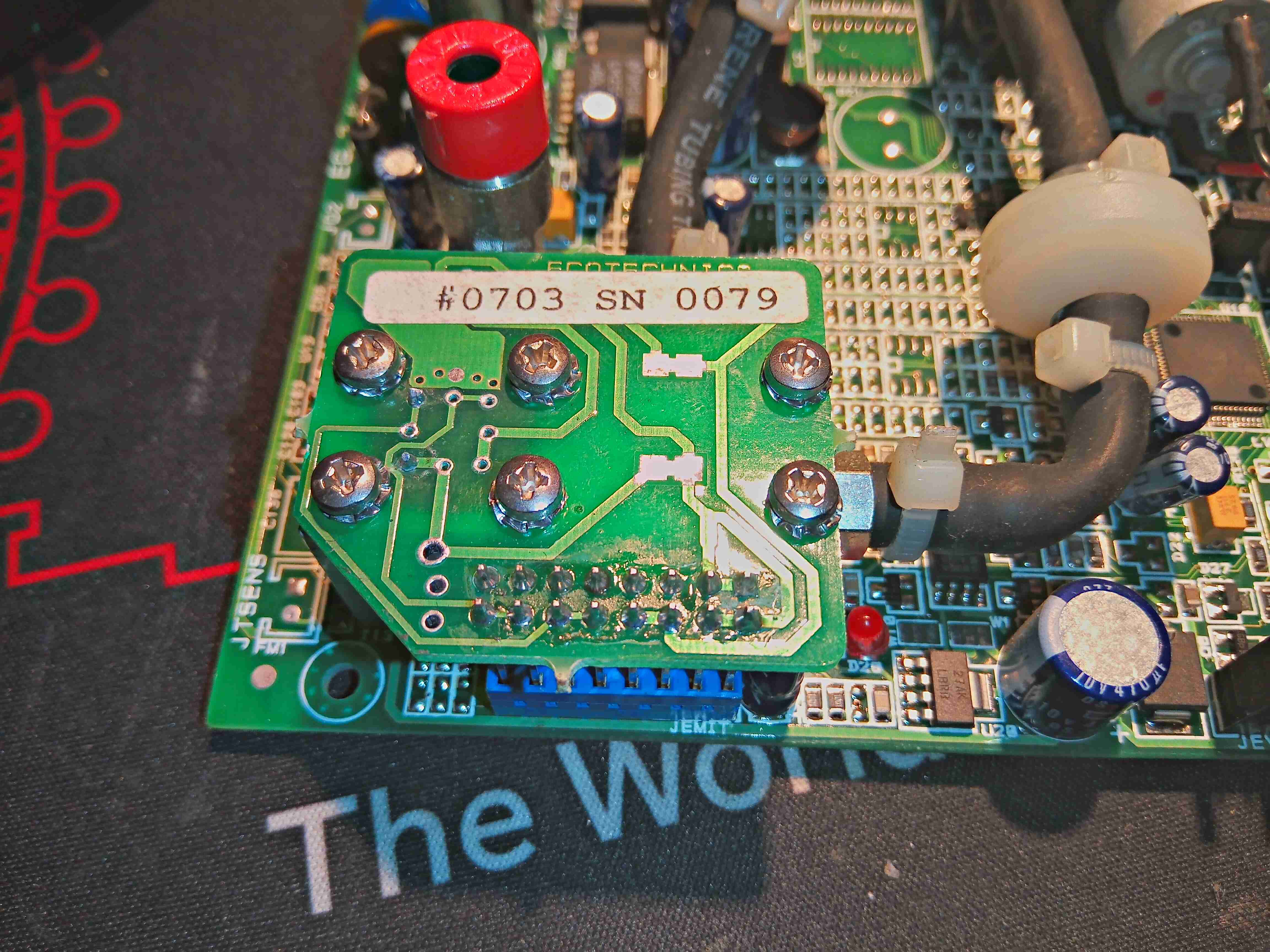
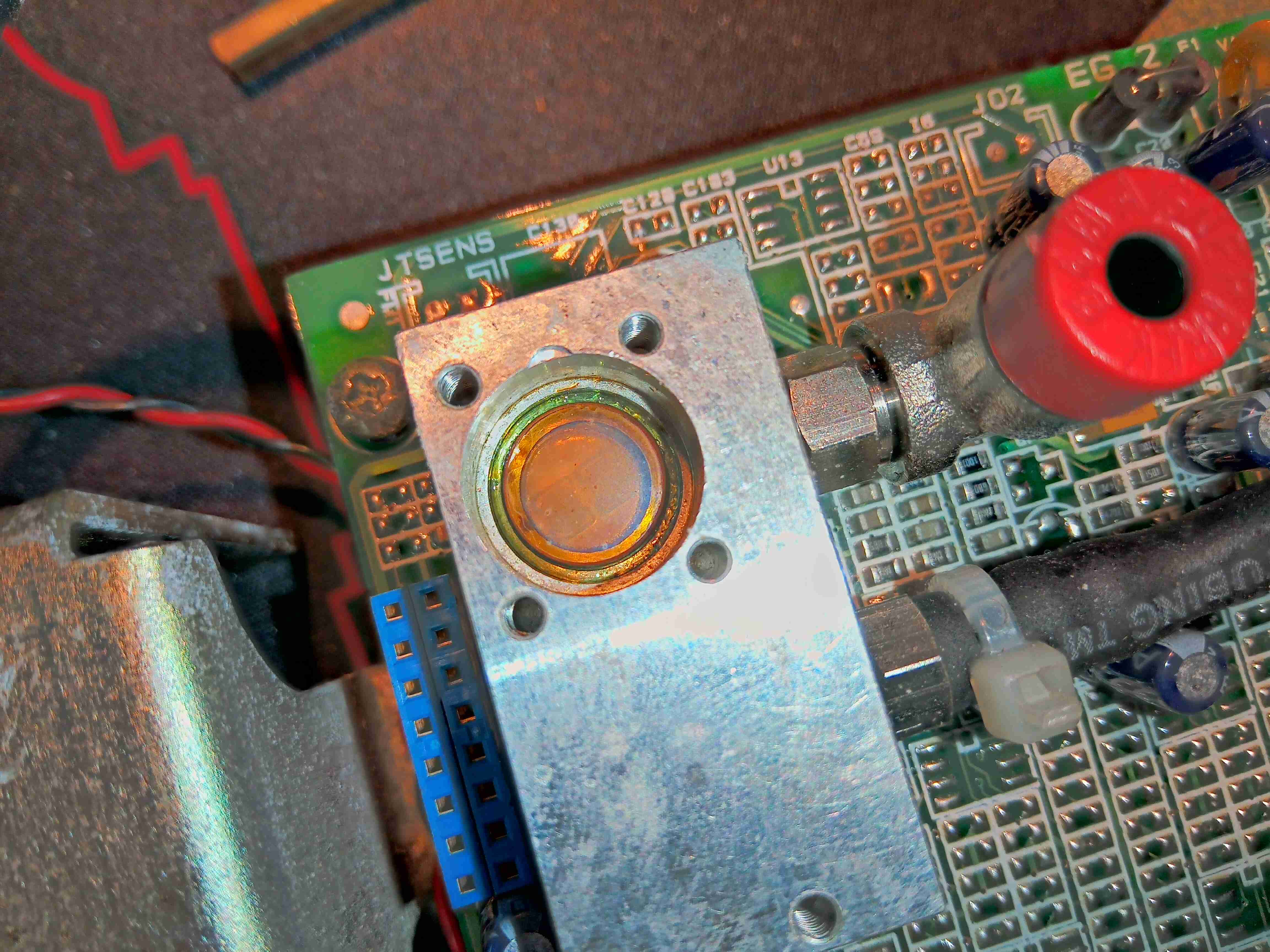
Gas Analysis Cell
Here’s the gas analyser cell itself, sandwiched under another board. There’s a temperature sensor on the side of the cell at the bottom, and even though there’s many pins on the header here, only a couple are actually used for the IR emitter.
IR Emitter
Removing the screws from the top allows the board to be removed, which exposes the Mid-IR emitter component with an exposed element. This looks to be very fragile, so I won’t be messing with this much. From metering the connections, this appears to be driven at about 2v from the microcontroller.
Top Of Gas Cell
The window into the gas cell looks to be made of something exotic – considering the IR application & the colour, this is probably Zinc Selenide.
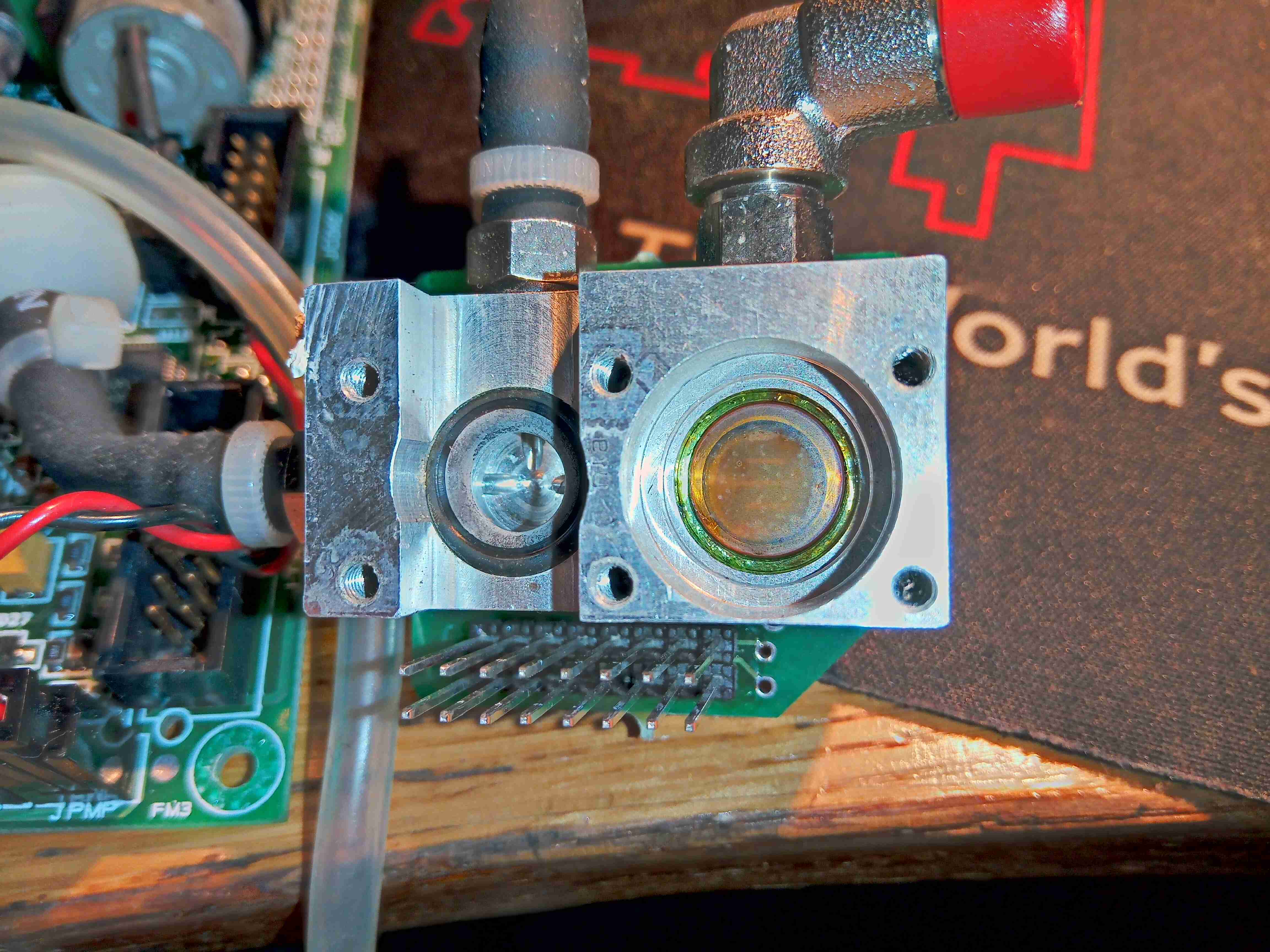
Gas Test Cell
Removing some more screws on the bottom exposes the bottom of the cell with another IR window, and an O-Ring where a pressure sensor sits.
Output Amplifiers
There’s a couple of very accurate LT1884 Rail-To-Rail Precision Op-Amps next to the cell, most likely used to measure the output from the sensor itself.
Mid-IR Sensor & Pressure Sensor
Finally, there is a dual-window thermopile sensor, and a pressure sensor. I wasn’t able to get any information on either of these, but I did find some ranges of sensors for Mid-IR measurement operations, that mentions a wavelength around 10µm for R-134a spectroscopy.
I will try to get this module going & measuring some gases, if I can work out how to talk to it – I already know the serial lines so it’s just working out a command set. If anyone has any information on these, please do get in touch! A service manual for the refrigerant machine this came out of would be good!
Tip Jar
If you’ve found my content useful, please consider leaving a donation by clicking the Tip Jar below!
All collected funds go towards new content & the costs of keeping the server online.