Here’s a jellybean chip – a DC motor driver. This device has all the logic to drive a small motor, such as that used to drive the tray of a CD drive in both directions. The control logic is at the bottom of the die, while the main power transistors are at the top, in H-Bridge formation.
Here’s a very common chip used in older LCD monitors. This converts the incoming VGA signal into LVDS for the panel itself.
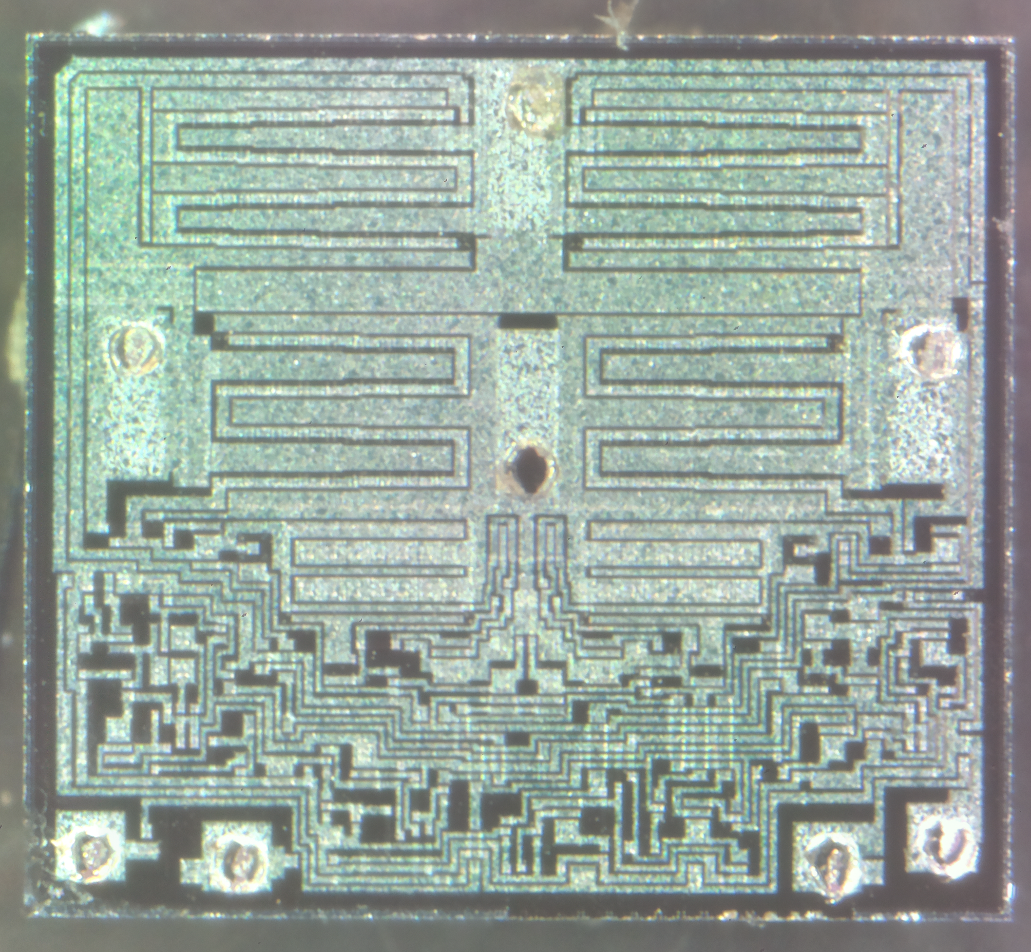
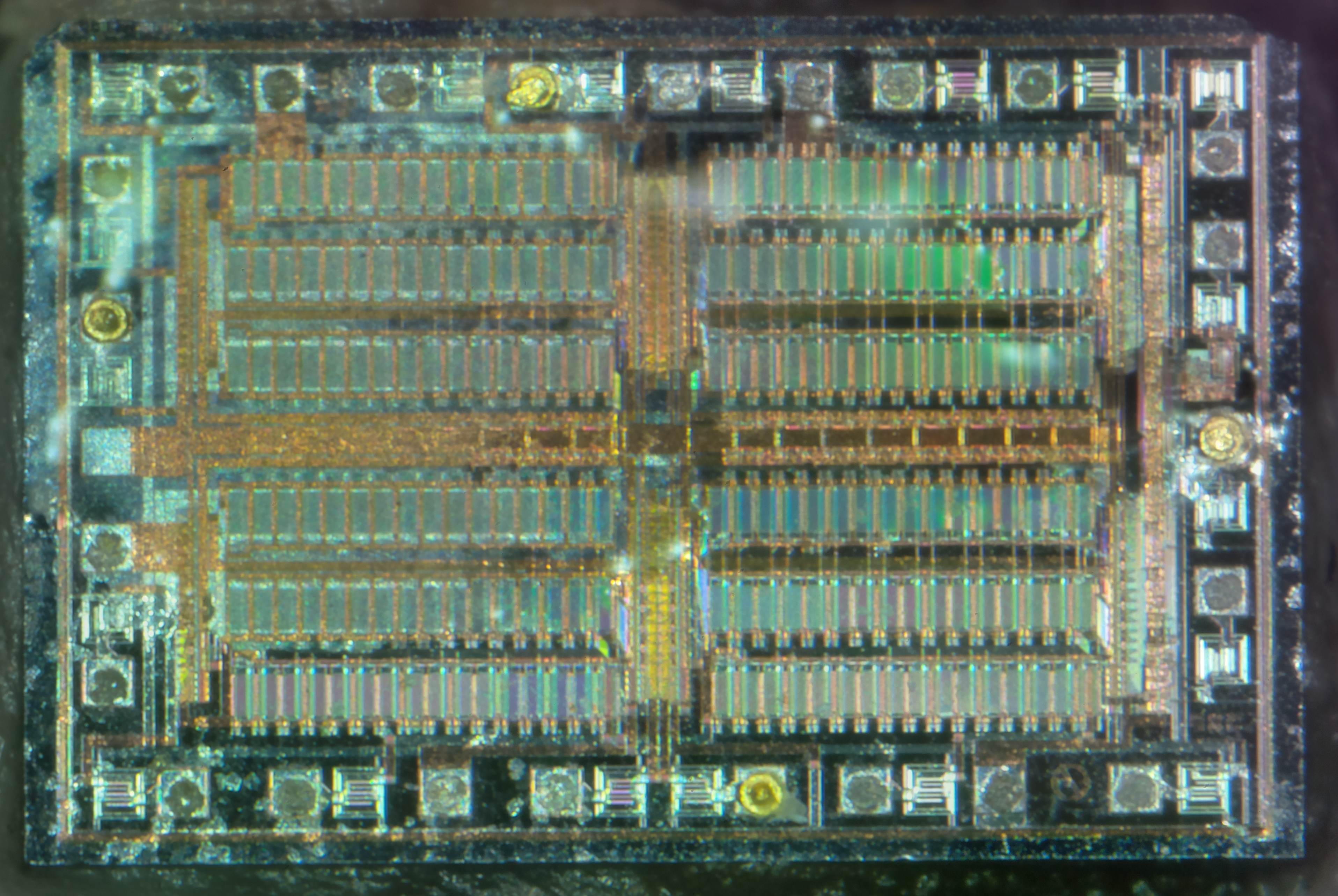
gmZAN3 Die
The gmZAN3 is a graphics processing IC for Liquid Crystal Display (LCD) monitors at XGA resolution. It provides all key IC functions required for the highest quality LCD monitors. On-chip functions include
a high-speed triple-ADC and PLL, a high quality zoom and shrink scaling engine, an on-screen display (OSD) controller and digital color controls.
It’s been 4 months since I did a rejig of my storage server, installing a new 16-port SATA HBA to support the disk drives. I mentioned the factory fan the card came with in my previous post, and I didn’t have many hopes of it surviving long.
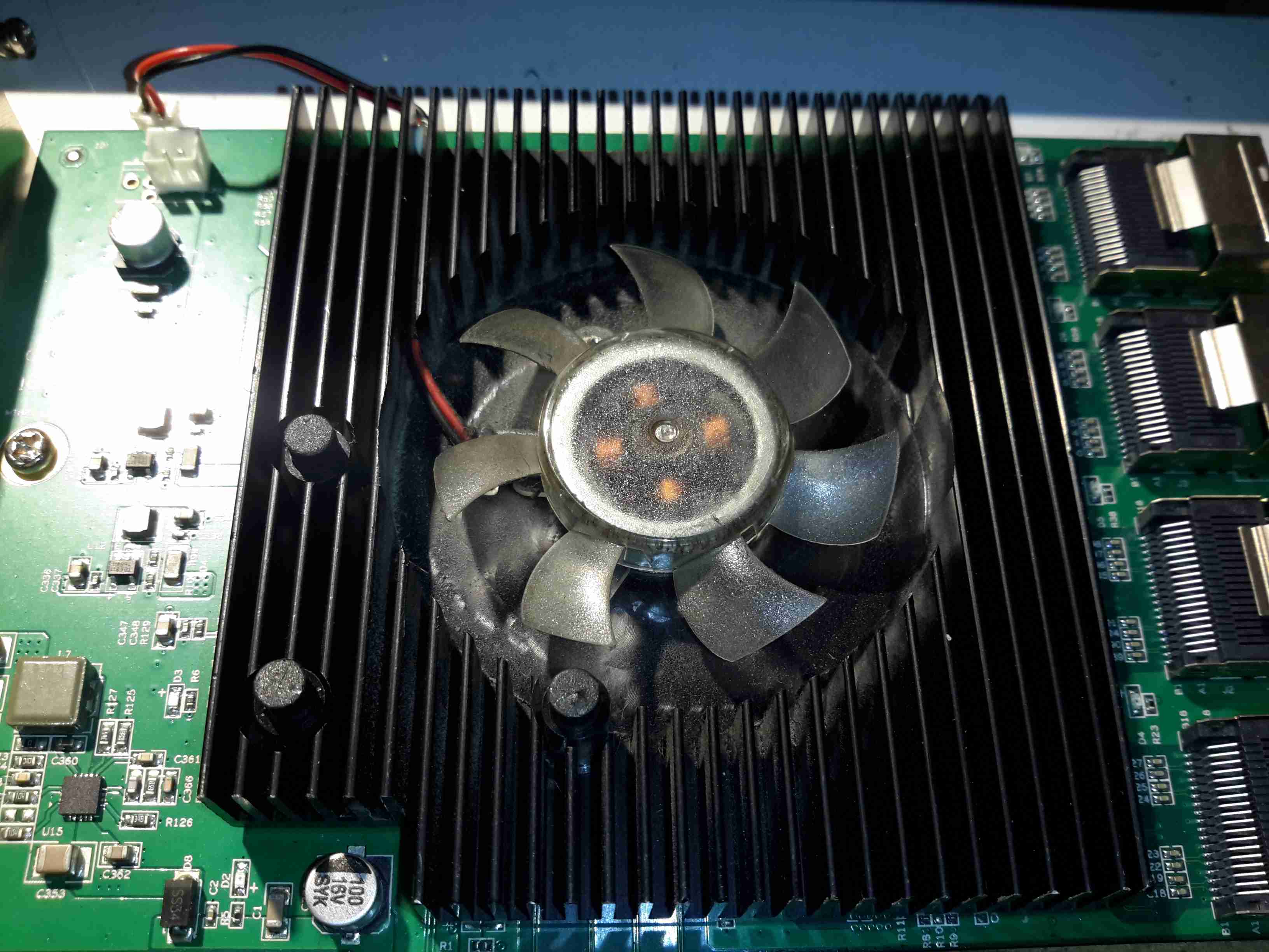
Heatsink
The heatsink card has barely had enough time to accumulate any grime from the air & the fan has already failed!
There’s no temperature sensing or fan speed sensing on this card, so a failure here could go unnoticed, and under load without a fan the heatsink becomes hot enough to cause burns. (There are a total of 5 large ICs underneath it). This would probably cause the HBA to overheat & fail rather quickly, especially when under a high I/O load, with no warning. In my case, the bearings in the fan failed, so the familiar noise of a knackered sleeve bearing fan alerted me to problems.
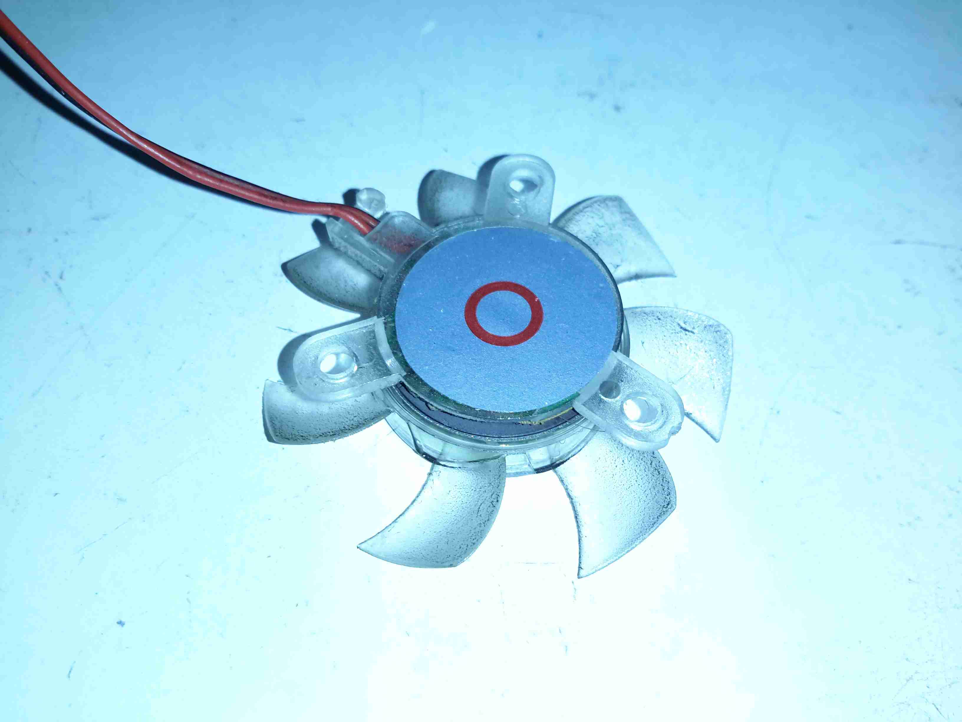
Replacement Fan
A replacement 80mm Delta fan has been attached to the heatsink in place of the dead fan, and this is plugged into a motherboard fan header, allowing sensing of the fan speed. The much greater airflow over the heatsink has dramatically reduced running temperatures. The original fan probably had it’s bearings cooked by the heat from the card as it’s airflow capability was minimal.
Fan Rear
Here’s the old fan removed from the heatsink. The back label, usally the place where I’d expect to find some specifications has nothing but a red circle. This really is the cheapest crap that the manufacturer could have fitted, and considering this HBA isn’t exactly cheap, I’d expect better.
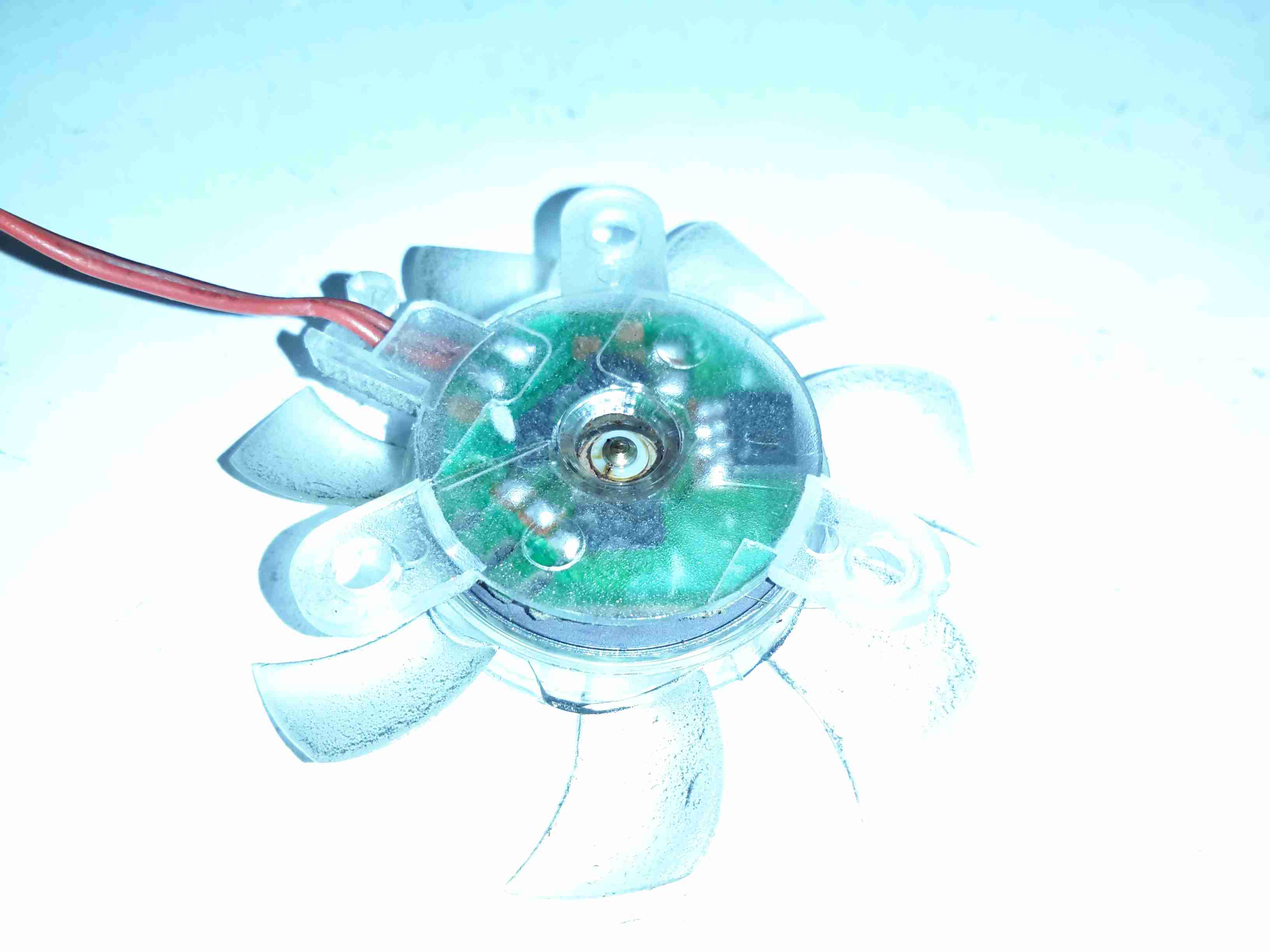
Bearings
Peeling off the back label reveals the back of the bearing housing, with the plastic retaining clip. There’s some sign of heat damage here, the oil has turned into gum, all the lighter fractions having evaporated off.
Rotor
The shaft doesn’t show any significant damage, but since the phosphor bronze bearing is softer, there is some dirt in here which is probably a mix of degraded oil & bearing material.
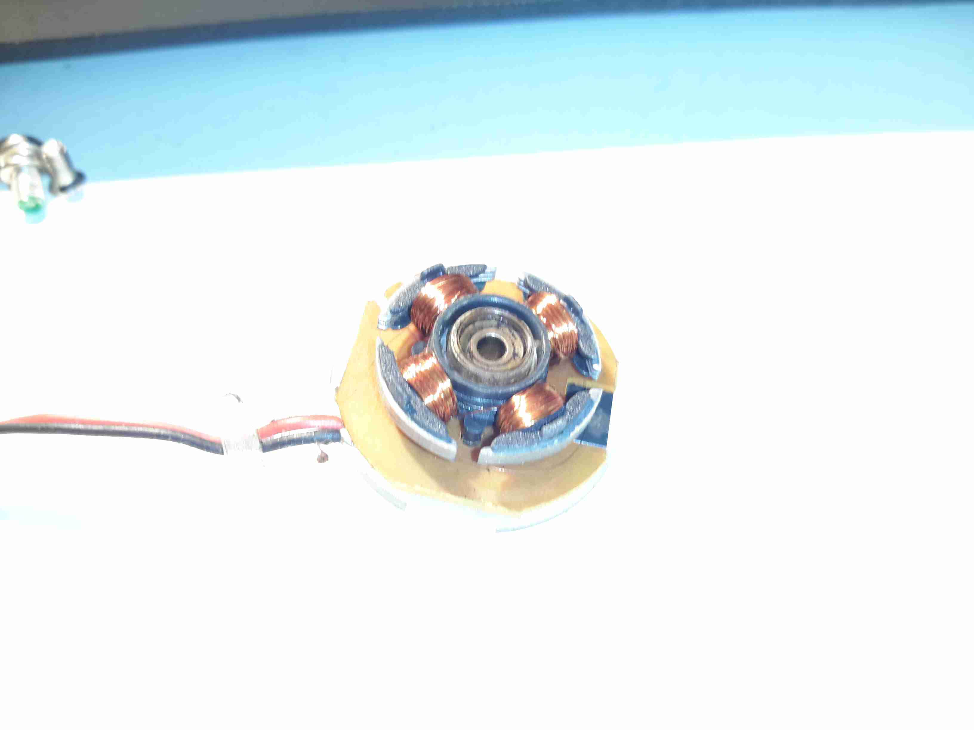
Stator & Bearing
There’s more gunge around the other end of the bearing & it’s been worn enough that side play can be felt with the shaft. In ~3000 hours running this fan is totally useless.
I recently got the latest upgrade from Virgin Media, 200Mbit DL / 20Mbit UL, and to get this I was informed I’d have to buy their latest hardware, since my existing CPE wouldn’t be able to handle the extra 5Mbit/s upload speed. (My bullshit detector went off pretty hard at that point, as the SuperHub 2 hardware is definitely capable of working fine with 20Mbit/s upload rates). Instead of having to return the old router, I was asked to simply recycle it, so of course the recycling gets done in my pretty unique way!
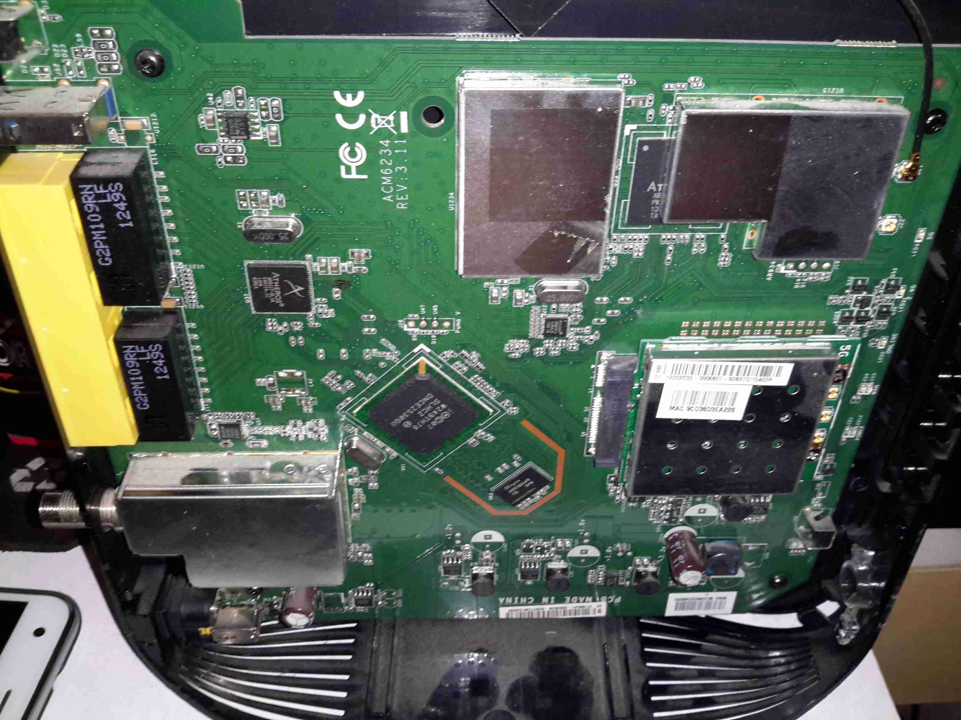
Mainboard
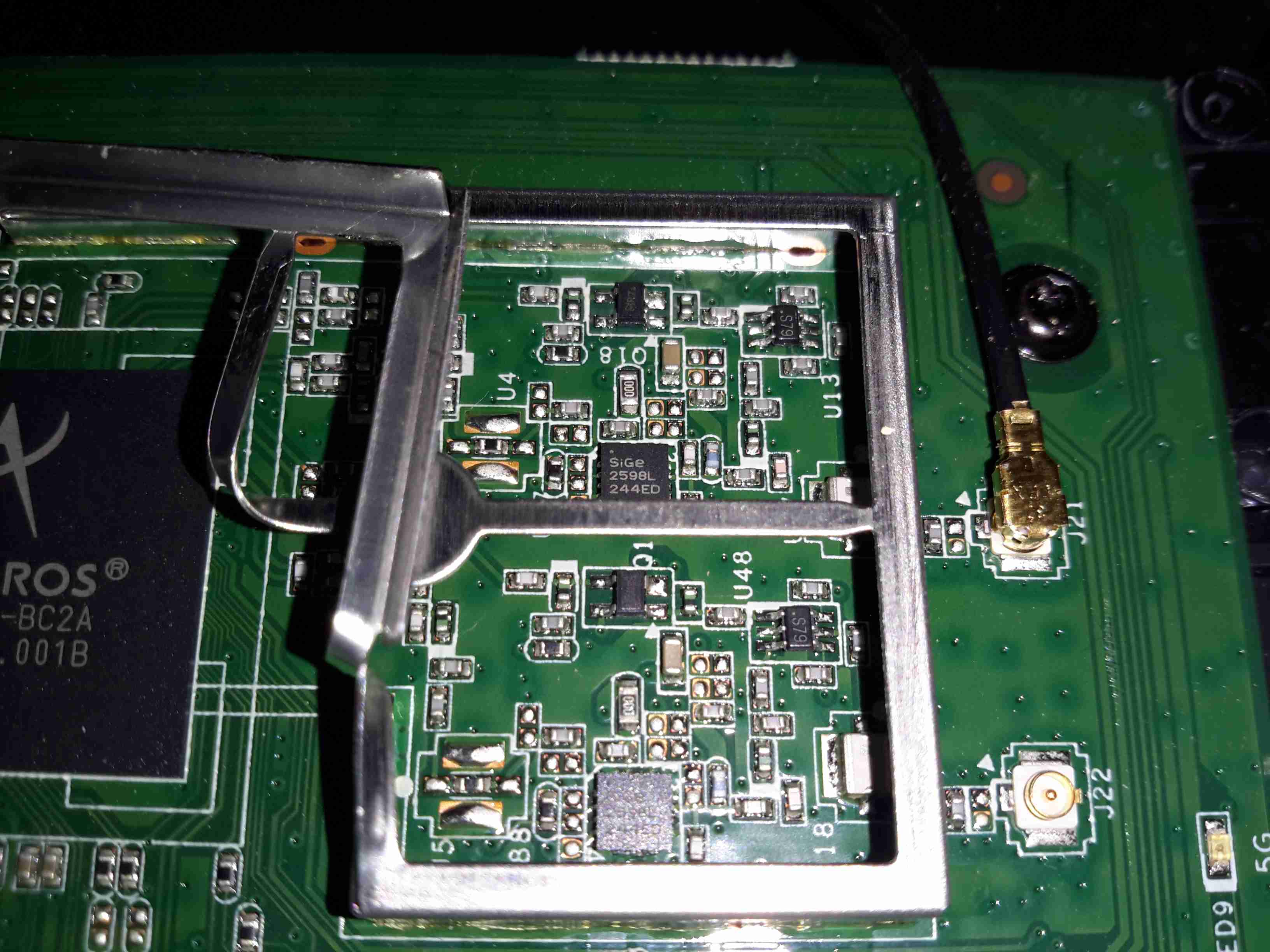
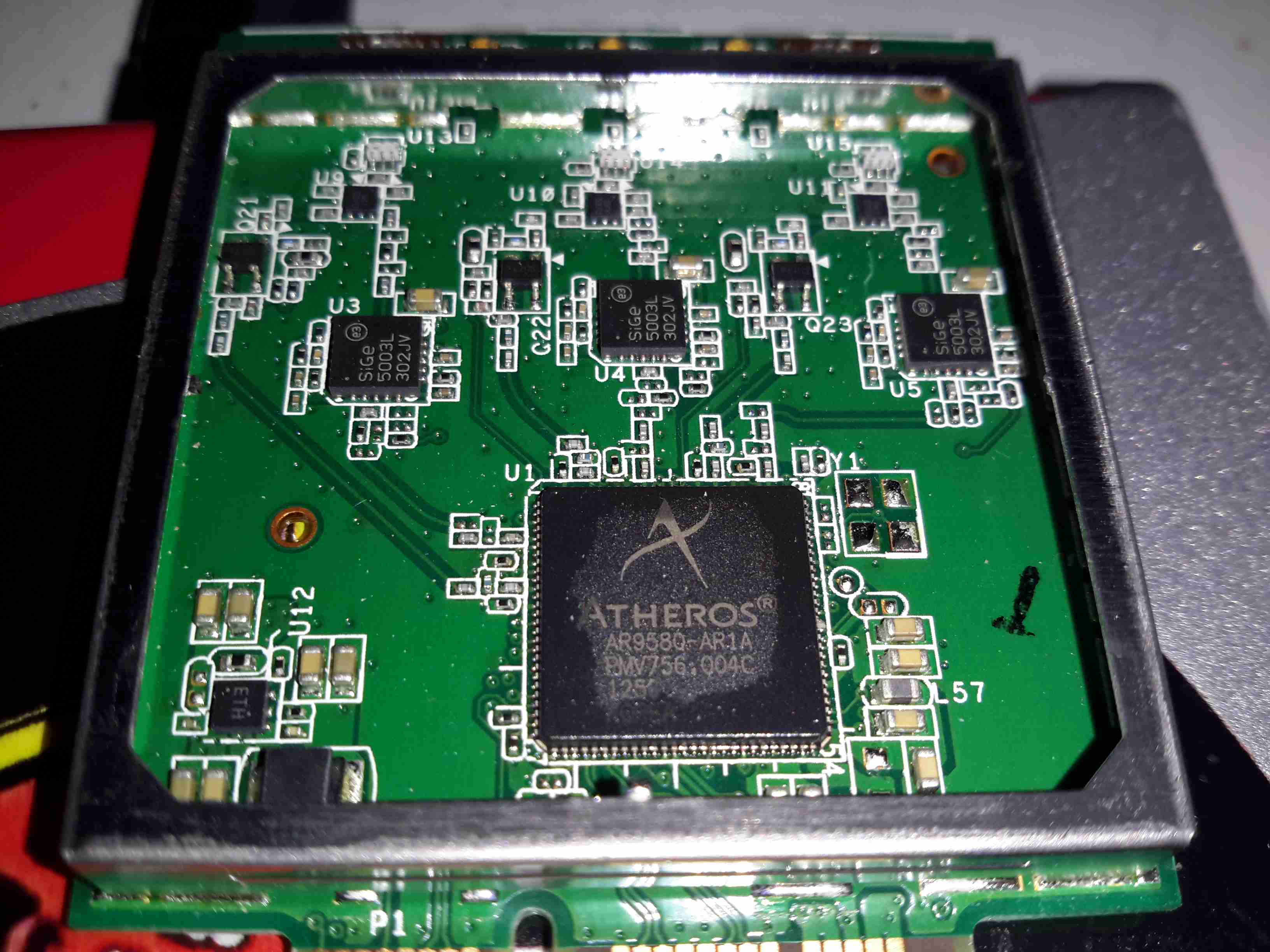
The casing of these units is held together by a single screw & a metric fuckton of plastic clips, disassembly is somewhat hindered by the radio antennas being positioned all over both sides of the casing. Once the side is off, the mainboard is visible. The DOCSIS frontend is lower left, centre is the Intel PUMA 5 Cable Modem SoC with it’s RAM just to the lower right. The right side of the board is taken up by both of the WiFi radio frontends, the 5GHz band being covered by a Mini PCIe card.
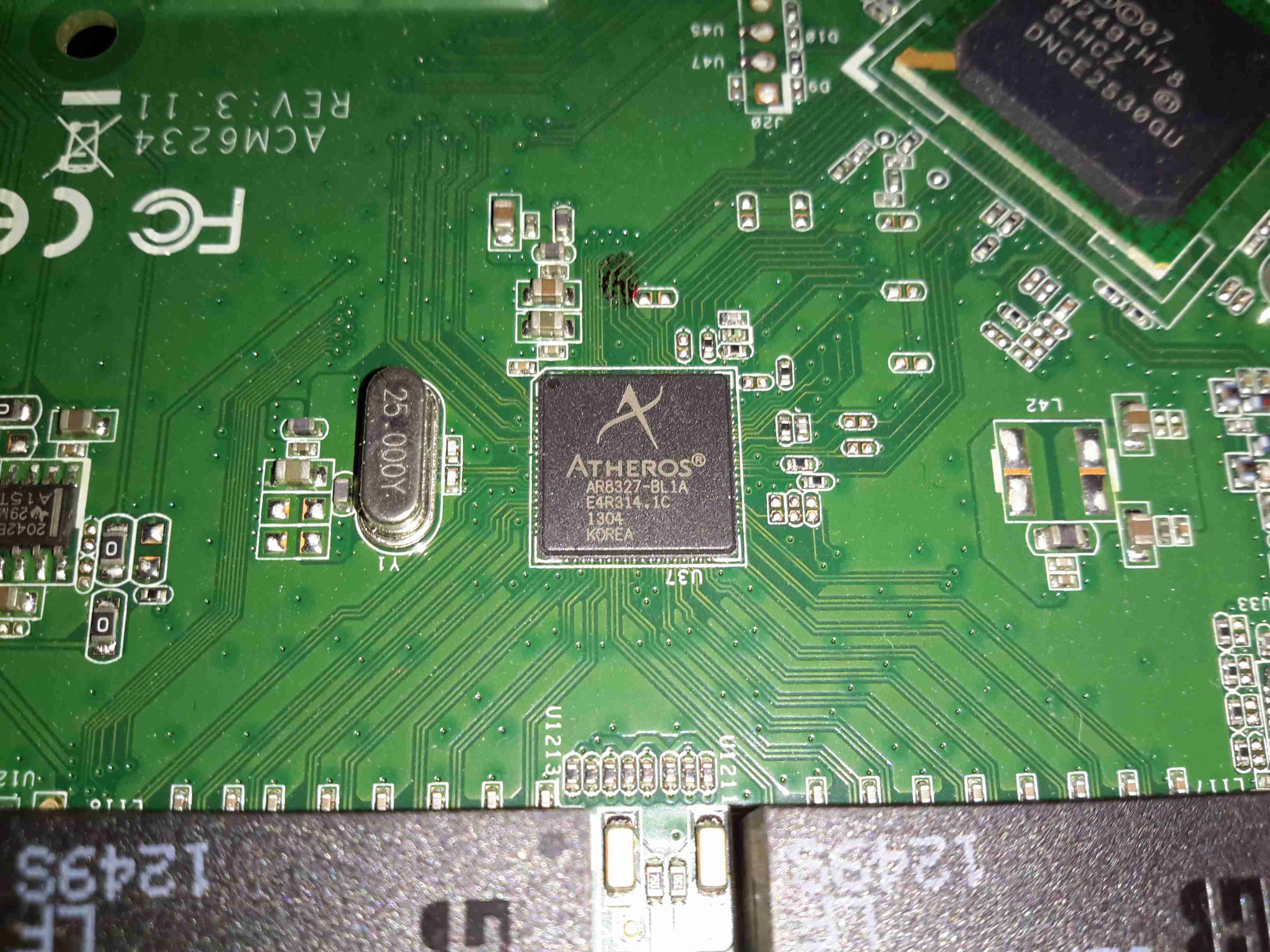
Atheros Gigabit Switch
The 4 gigabit Ethernet ports on the back are serviced by an Atheros AR8327 Managed Layer 3 switch IC, which seems to be a pretty powerful device:
The AR8327 is the latest in high performance small network switching. It is ultra low power, has extensive routing and data management functions and includes hardware NAT functionality (AR8327N). The AR8327/AR8327N is a highly integrated seven-port Gigabit Ethernet switch with a fully non-blocking switch fabric, a high-performance lookup unit supporting 2048 MAC addresses, and a four-traffic class Quality of Service (QoS) engine. The AR8327 has the flexibility to support various networking applications. The AR8327/AR8327N is designed for cost-sensitive switch applications in wireless AP routers, home gateways, and xDSL/cable modem platforms.
Unfortunately most of the features of this router are locked out by VM’s extremely restrictive firmware. With any of their devices, sticking the VM supplied unit into modem mode & using a proper router after is definitely advised!
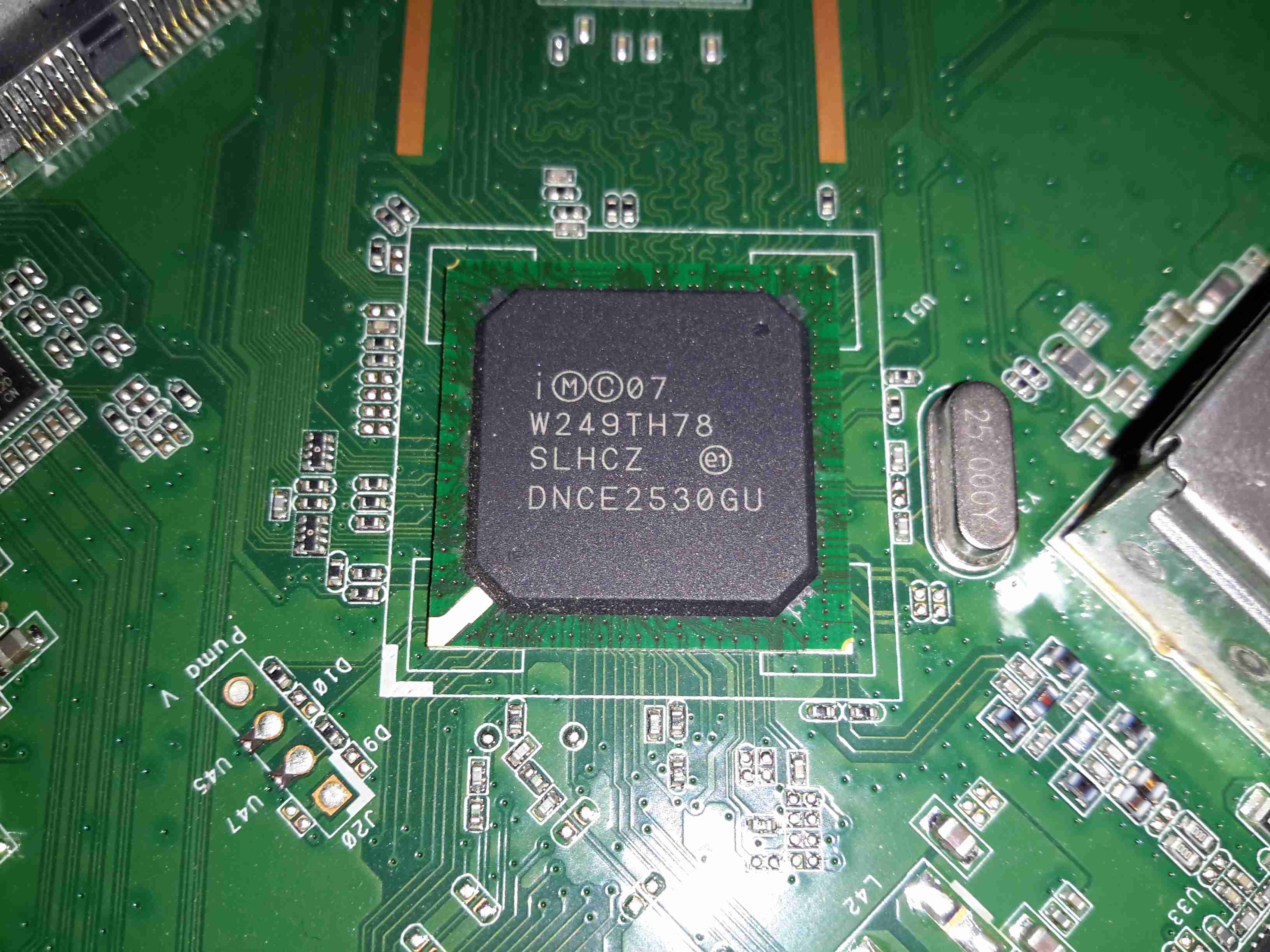
Intel Puma 5 CM CPU
The cable modem side of things is taken care of by the Intel PUMA 5 DNCE2530GU SoC. This appears to communicate with the rest of the system via the Ethernet switch & PCI Express for the 5GHz radio.
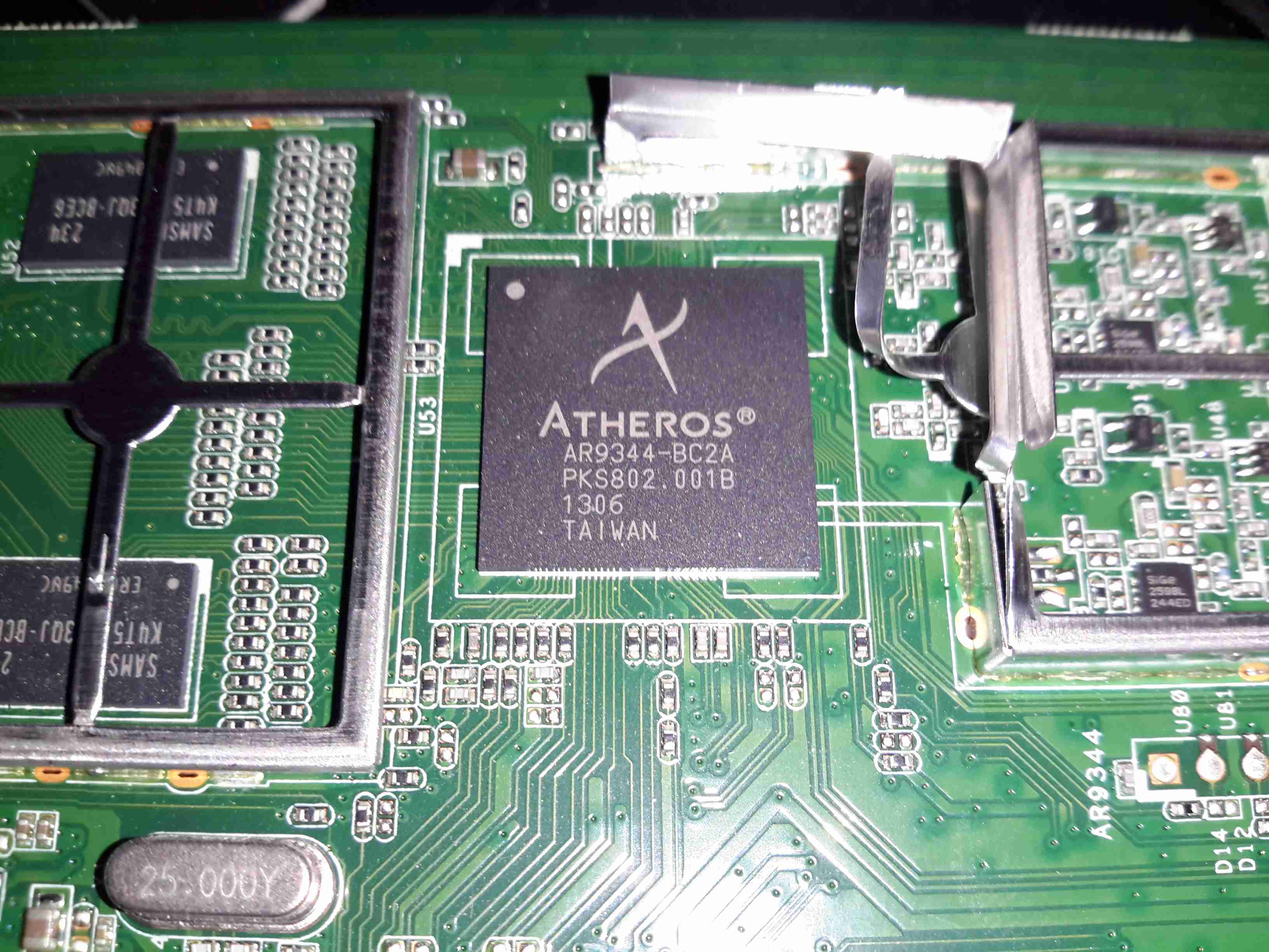
Atheros WiFi SoC
The 2.4GHz radio functionality is supplied by an Atheros AR9344 SoC, it’s RAM is to the left. This is probably handling all the router functions of this unit, but I can’t be certain.
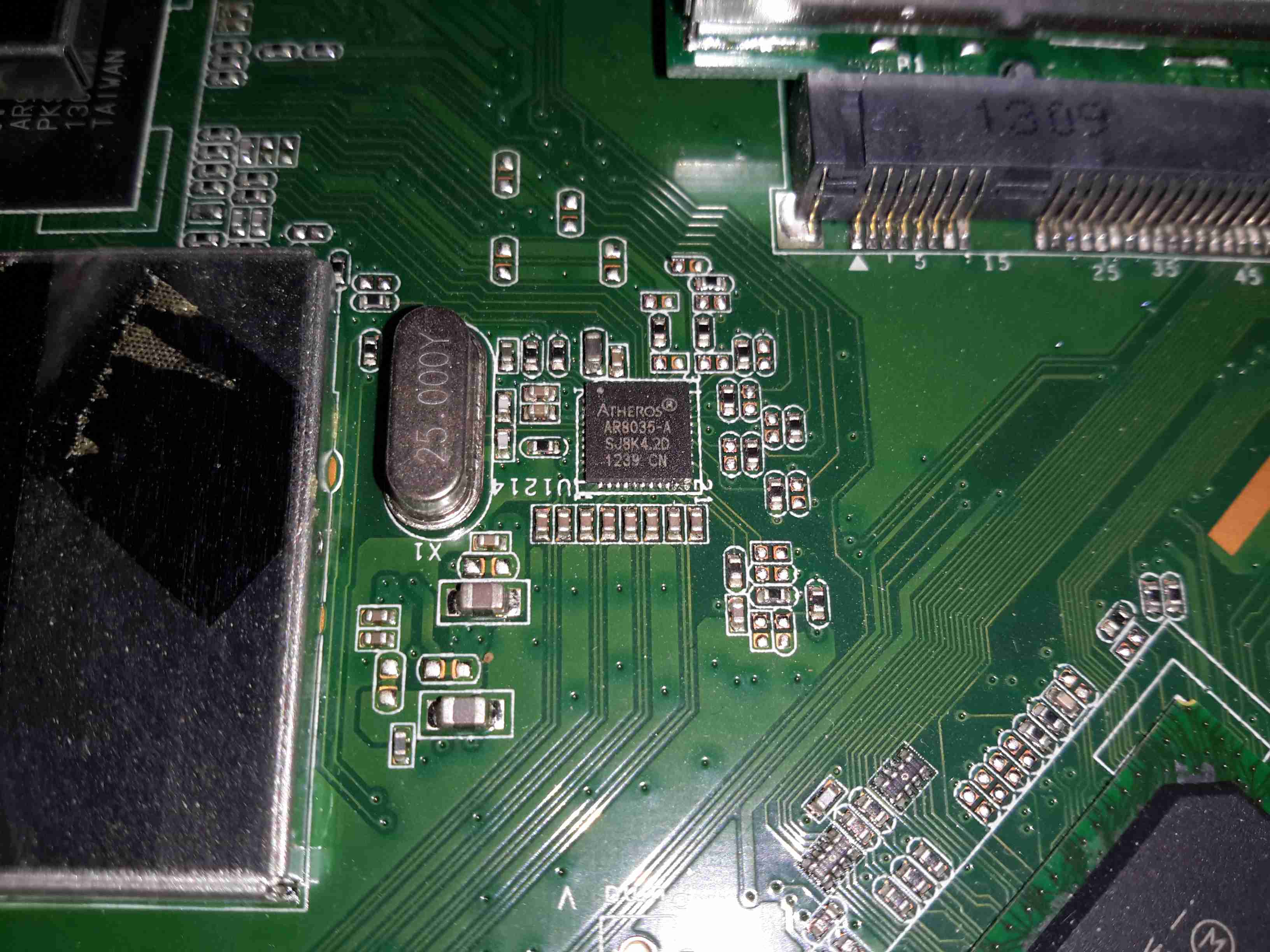
Atheros LAN PHY
A separate Ethernet PHY is located between the SoC & the switch IC.
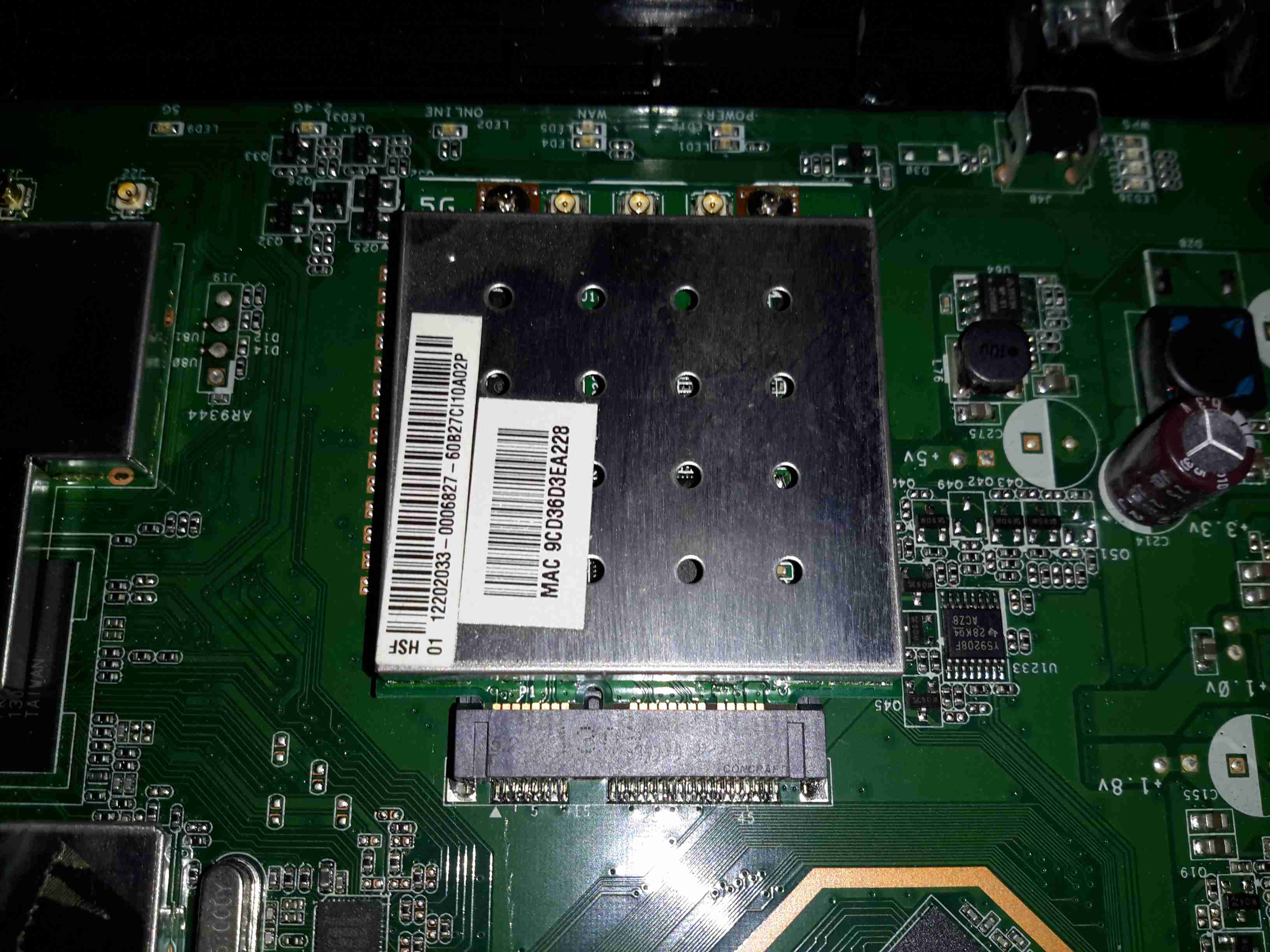
5GHz Radio Card
The 5GHz band is served by a totally separate radio module, in Mini PCIe format, although it’s a bit wider than standard. This module will probably be kept for reuse in another application.
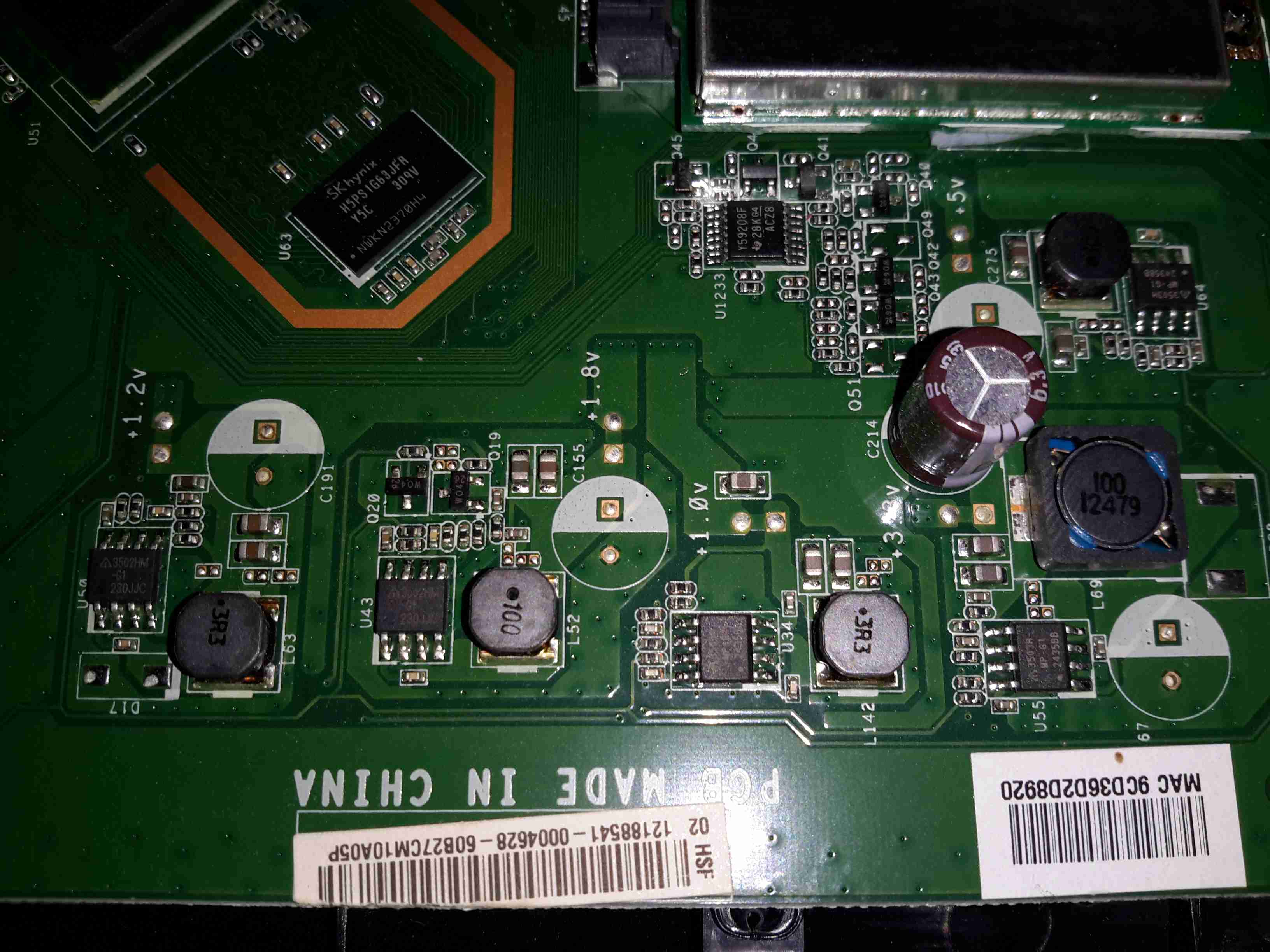
Power Supplies
All down the edge of the board are the multiple DC-DC converters to generate the required voltage rails.
MaxLinear MXL261 Frontend
The DOCSIS frontend is handled by a MaxLinar MXL261 Tuner/Demodulator. More on this IC in my decapping post 🙂
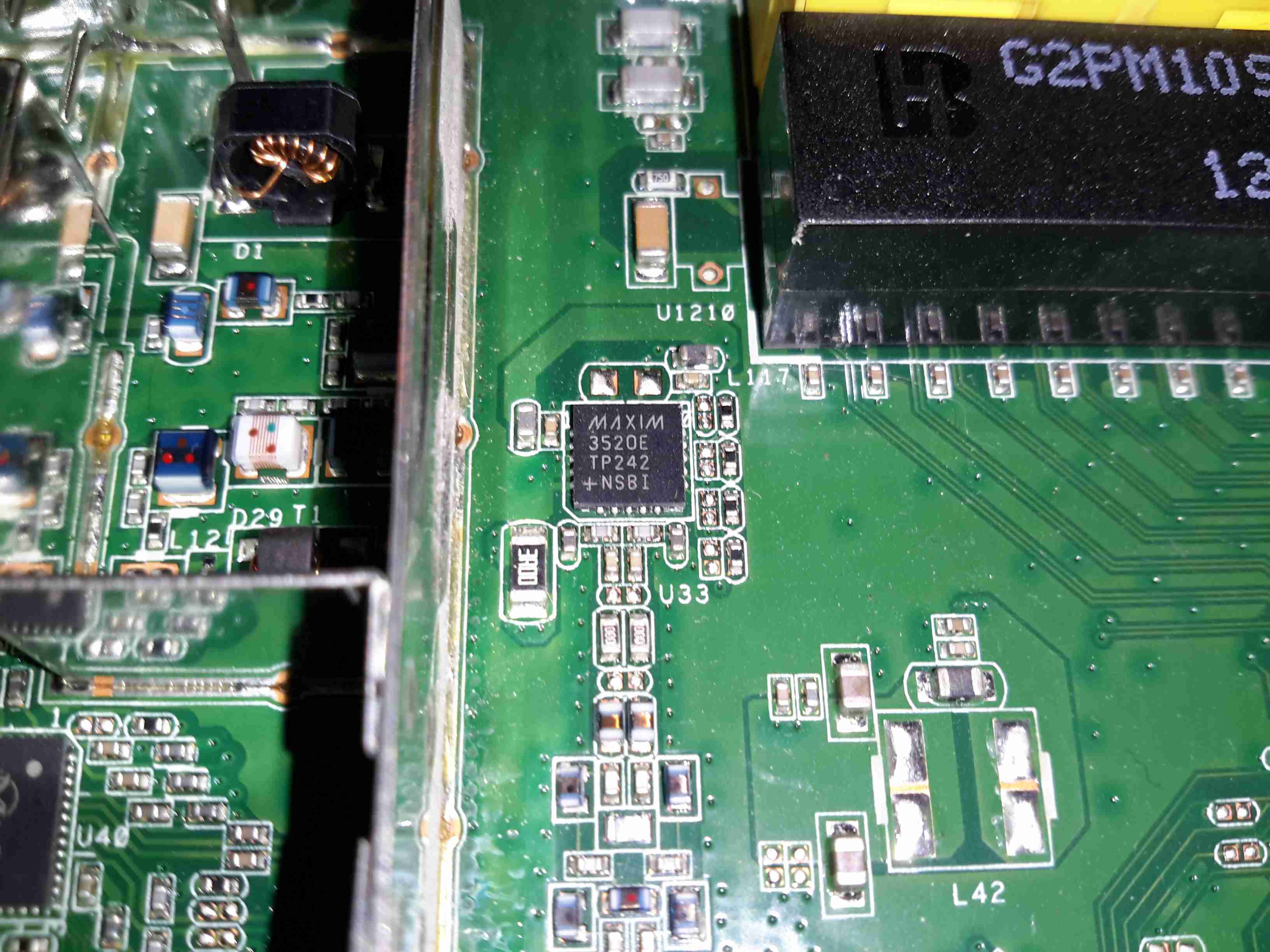
The Unknown One
I’ve honestly no idea what on earth this Maxim component is doing. It’s clearly connected via an impedance matched pair, and that track above the IC looks like an antenna, but nothing I search for brings up a workable part number.
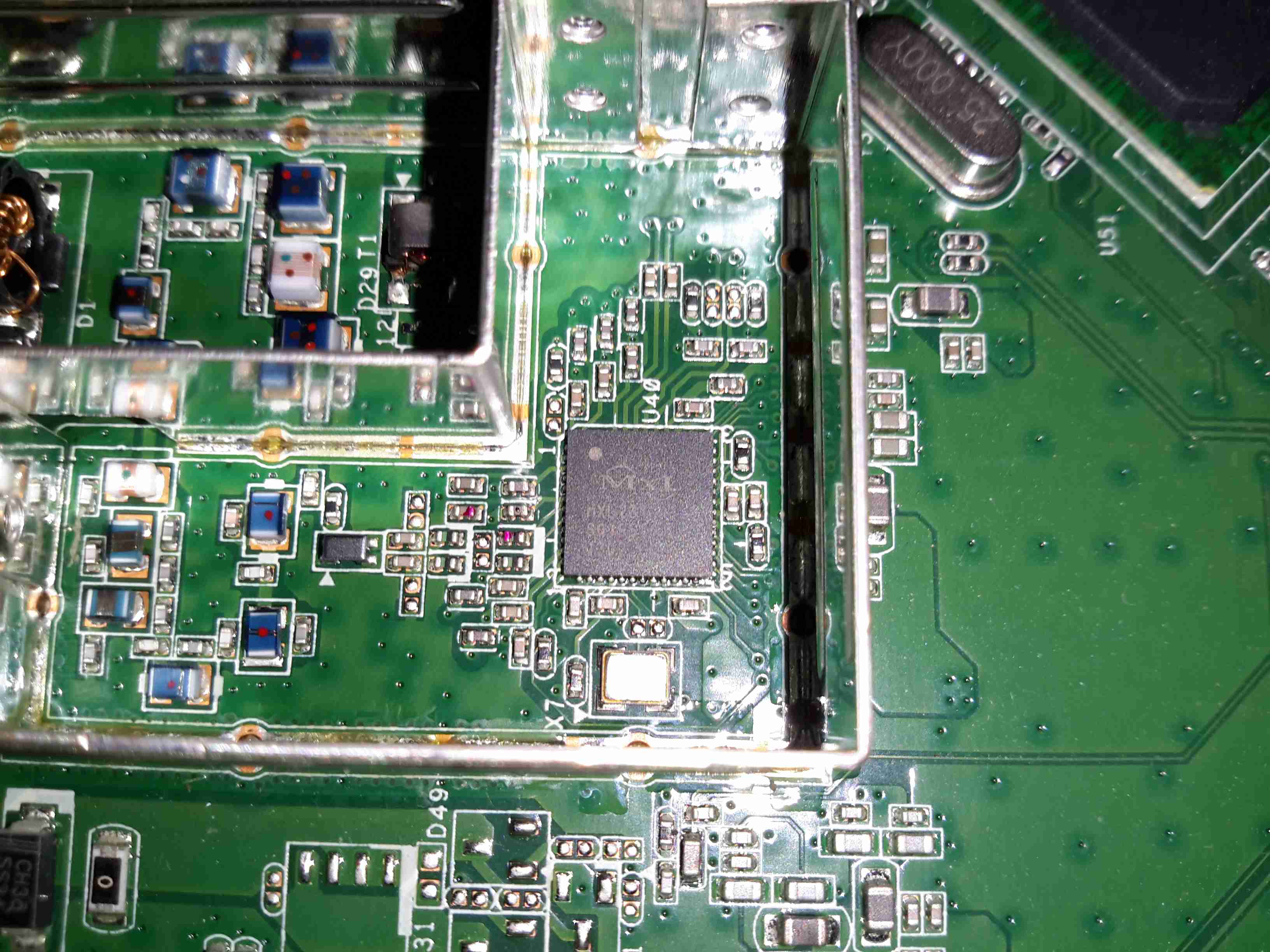
2.4GHz Frontend
The RF switching & TX amplifiers are under a shield, these PA chips are SiGe parts.
Atheros 5GHz Radio
Pretty much the same for the 5GHz radio, but with 3 radio channels.
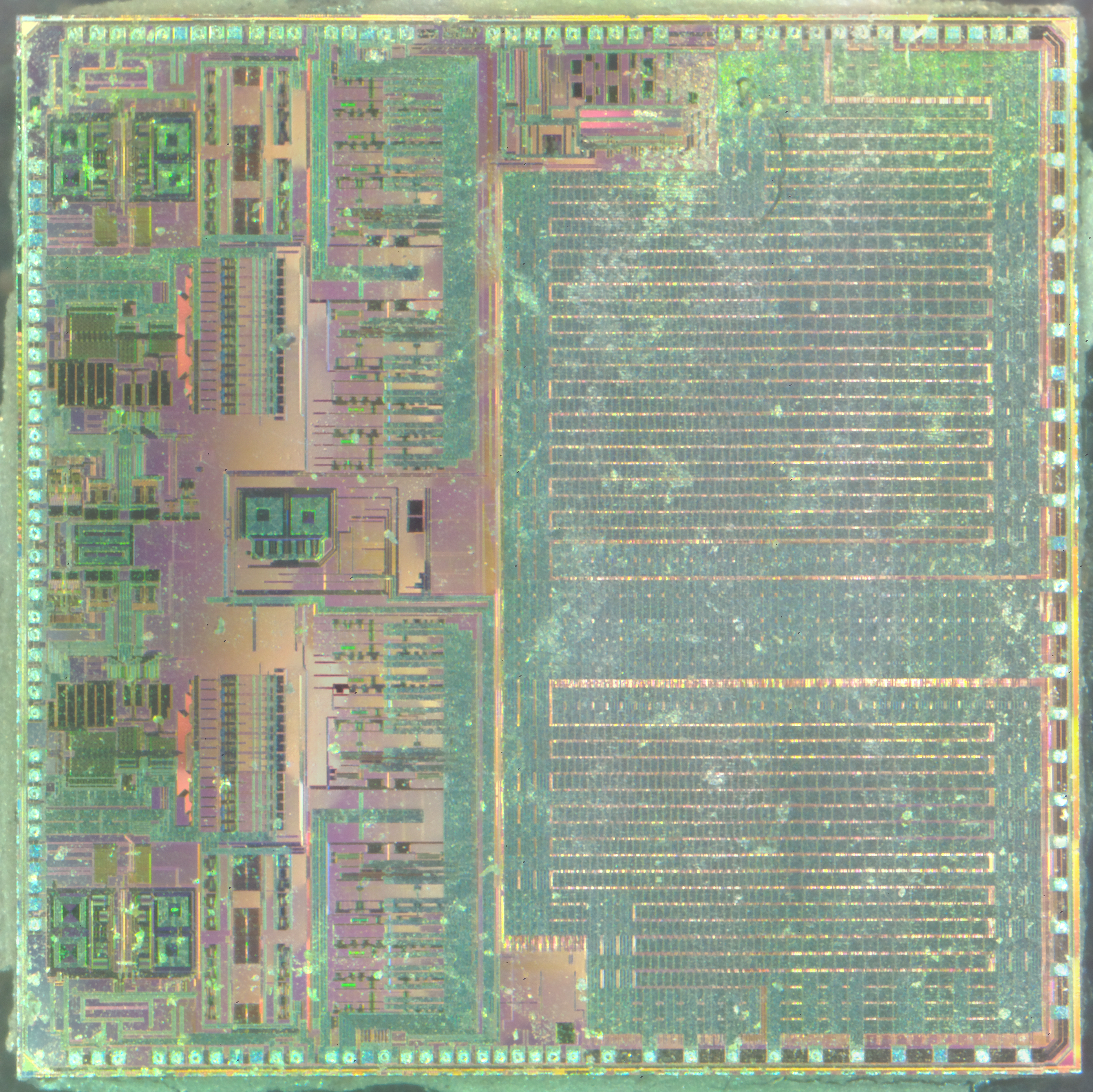
Time for more silicon pr0n! When Virgin Media supplied me with a new modem, they requested I “recycle” the old one, so naturally it got gutted for the component parts. This particular IC is the frontend of the RF tuner. Unfortunately no datasheet is available, but I did manage to find some info in a press release. The sections are clearly identifiable, the RF section is on the left, while the rest of the demodulating logic is hidden on the right under a metal layer.
MXL261 Die – Click to Embiggen!
The MxL261 is based on MaxLinear’s low-power, digital CMOS process RF and mixed-signal technology. It is a single-die, global standards, digital cable front end with integrated splitter, two 100MHz wideband tuners, four QAM demodulators and a four-channel-wide IF output.
Here’s a piece of tech that is growing all the more important in recent times, with devices with huge battery capacities, a quick charger. This unit supports Qualcomm’s Quick Charge 3 standard, where the device being charged can negotiate with the charger for a higher-power link, by increasing the bus voltage past the usual 5v.
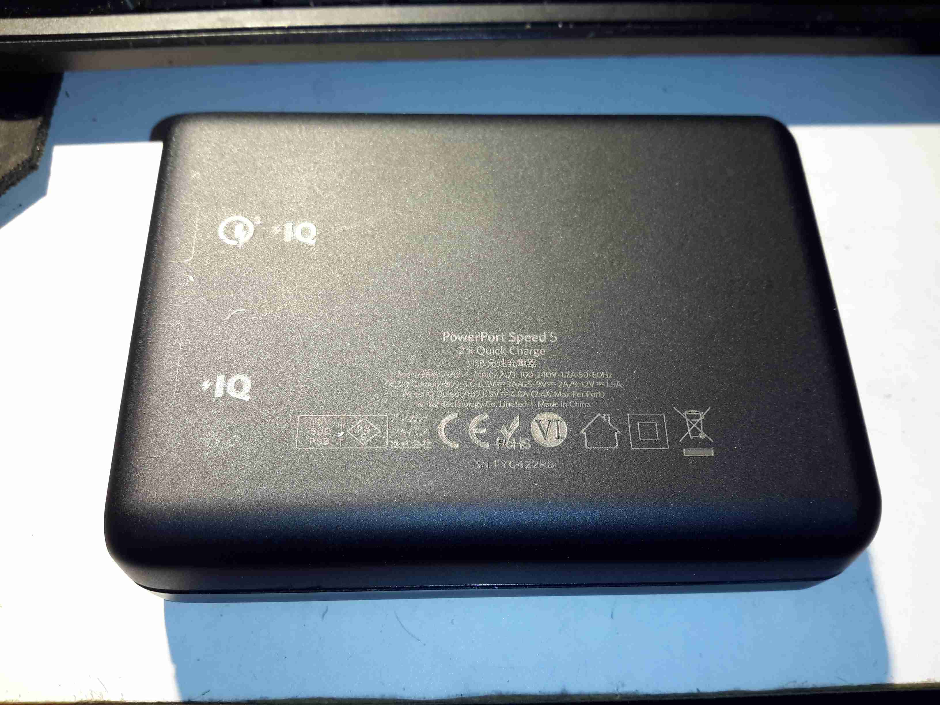
Rear
The casing feels rather nice on this unit, sturdy & well designed. All the legends on the case are laser marked, apart from the front side logo which is part of the injection moulding.
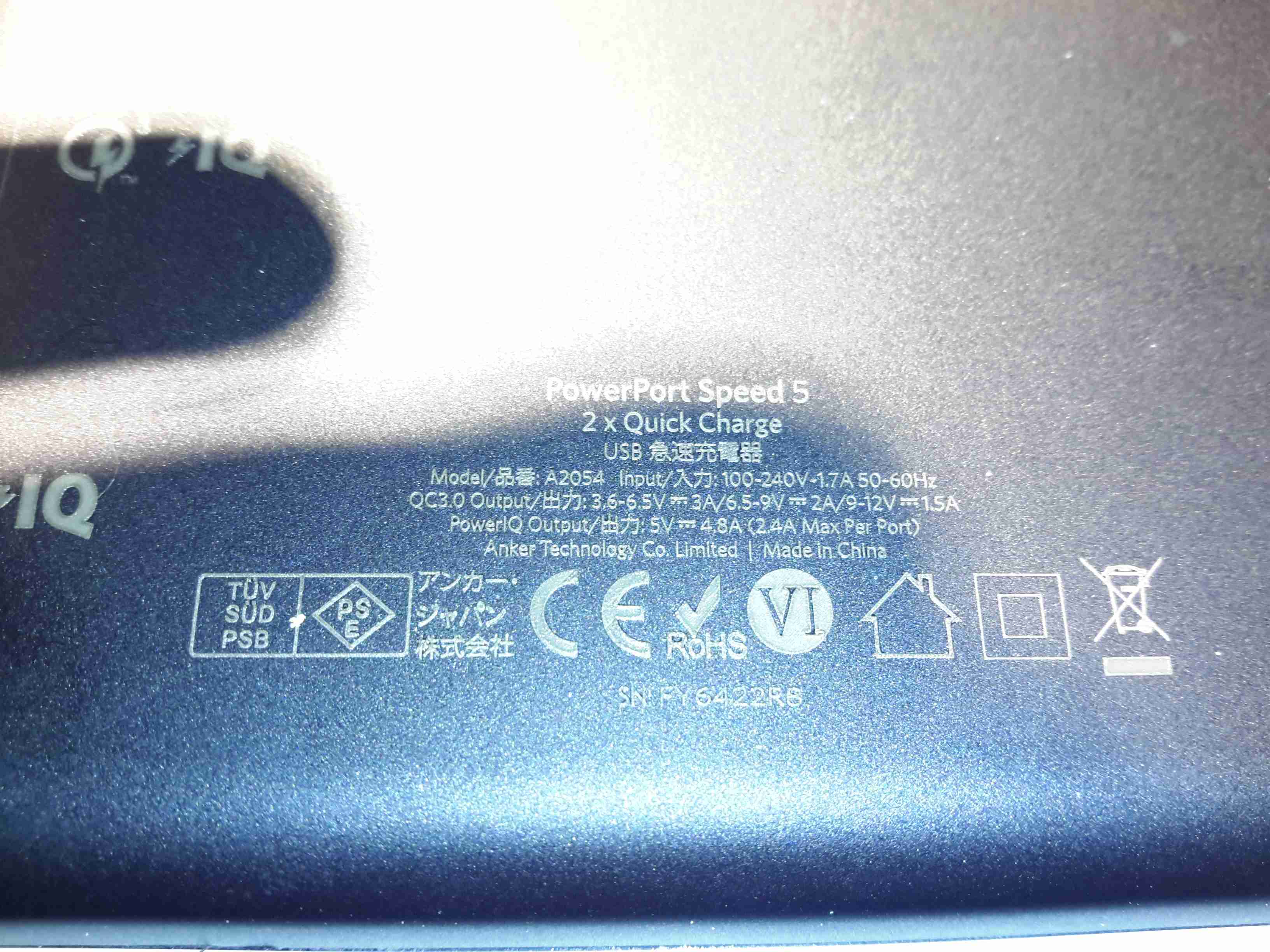
Specifications
The power capacity of this charger is pretty impressive, with outputs for QC3 from 3.6-6.5v at 3A, up to 12v 1.5A. Standard USB charging is limited at 4.8A for the other 3 ports.
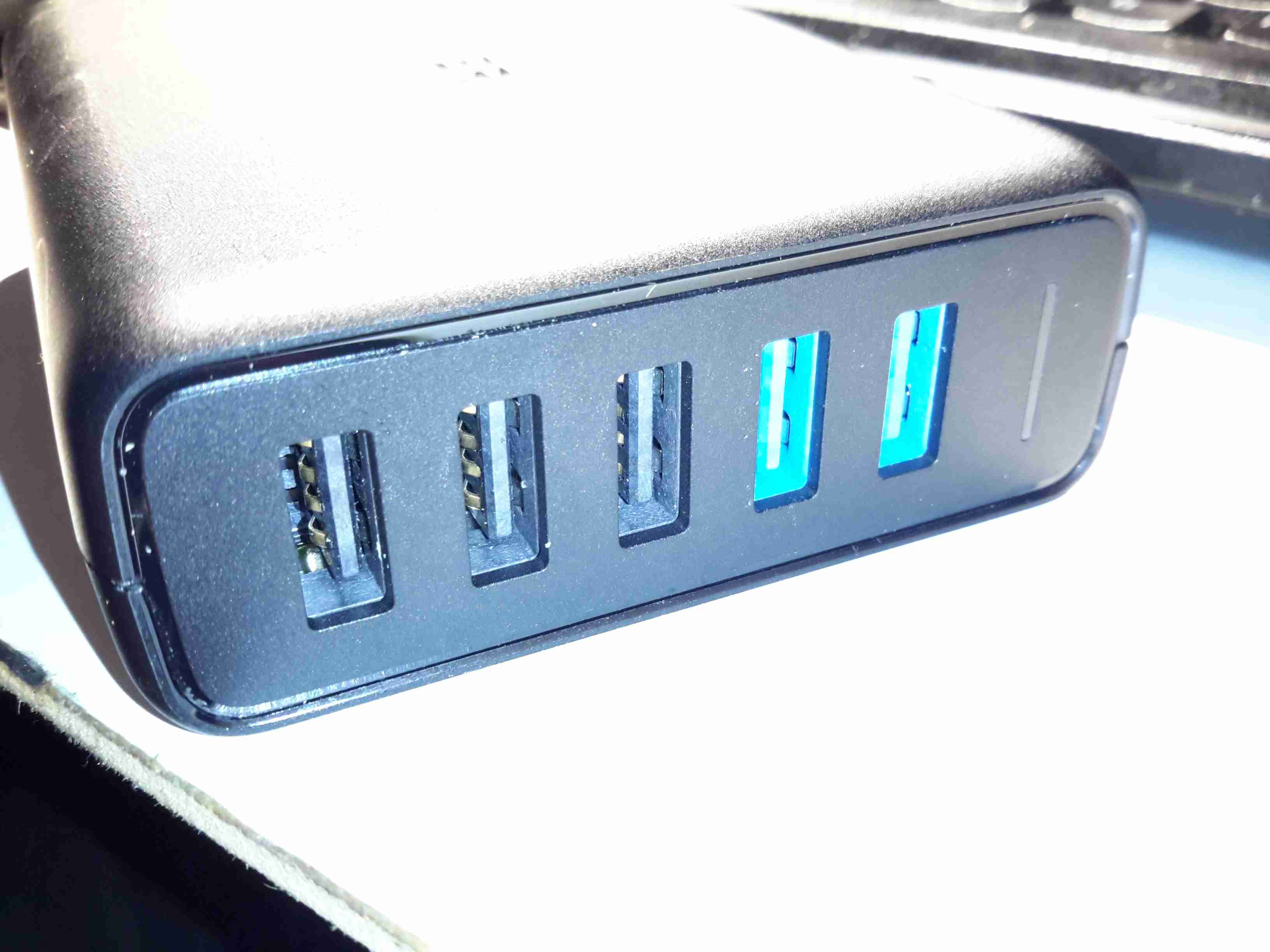
Ports
The two of the 5 USB ports are colour coded blue on the QC3 ports. The other 3 are standard 5v ports, the only thing that doesn’t make sense in the ratings is the overall current rating of the 5v supply (4.8A), and the rated current of each of the ports (2.4A) – this is 7.2A total rather than 4.8A.
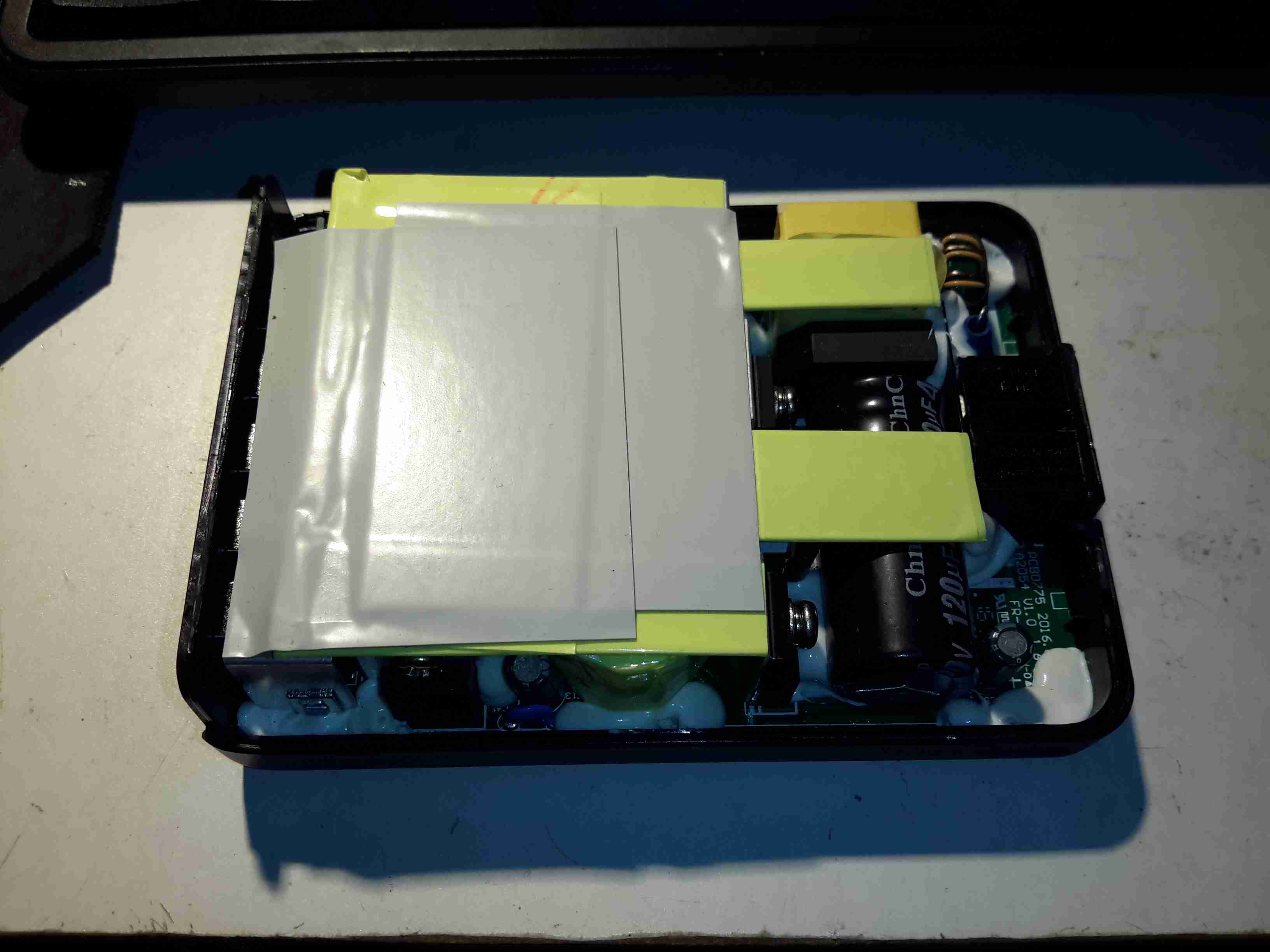
Top Removed
The casing is glued together at the seam, but it gave in to some percussive attack with a screwdriver handle. The inside of this supply is mostly hidden by the large heatspreader on the top.
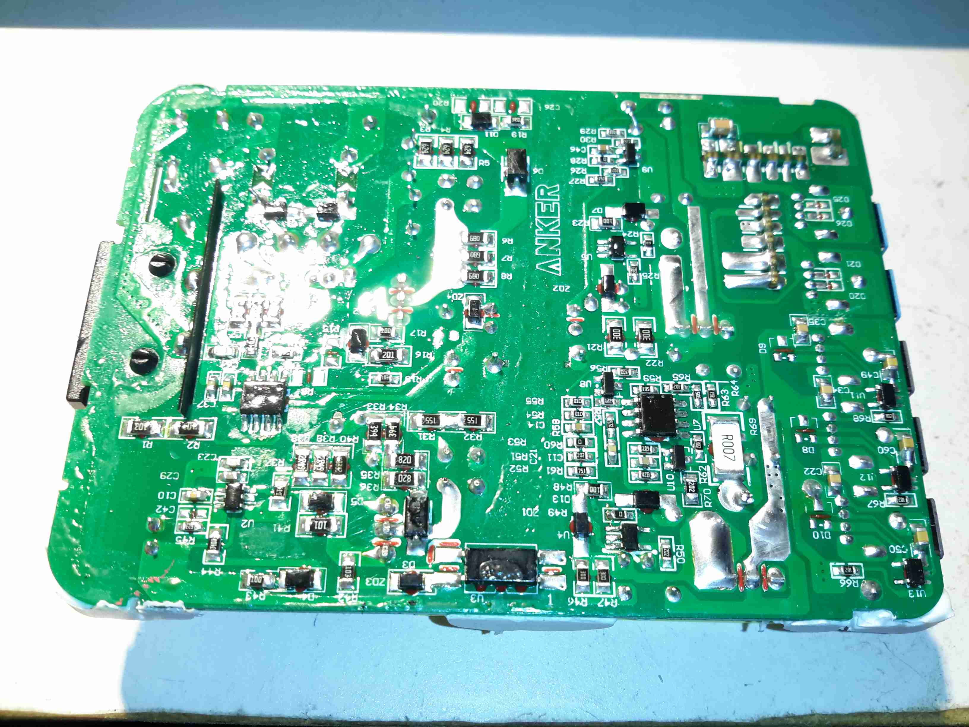
Main PCB Bottom
This is a nicely designed board, the creepage distances are at least 8mm between the primary & secondary sides, the bottom also has a conformal coating, with extra silicone around the primary-side switching transistor pins, presumably to decrease the chances of the board flashing over between the close pins.
On the lower 3 USB ports can be seen the 3 SOT-23 USB charge control ICs. These are probably similar to the Texas Instruments TPS2514 controllers, which I’ve experimented with before, however I can’t read the numbers due to the conformal coating. The other semiconductors on this side of the board are part of the voltage feedback circuits for the SMPS. The 5v supply optocoupler is in the centre bottom of the board.
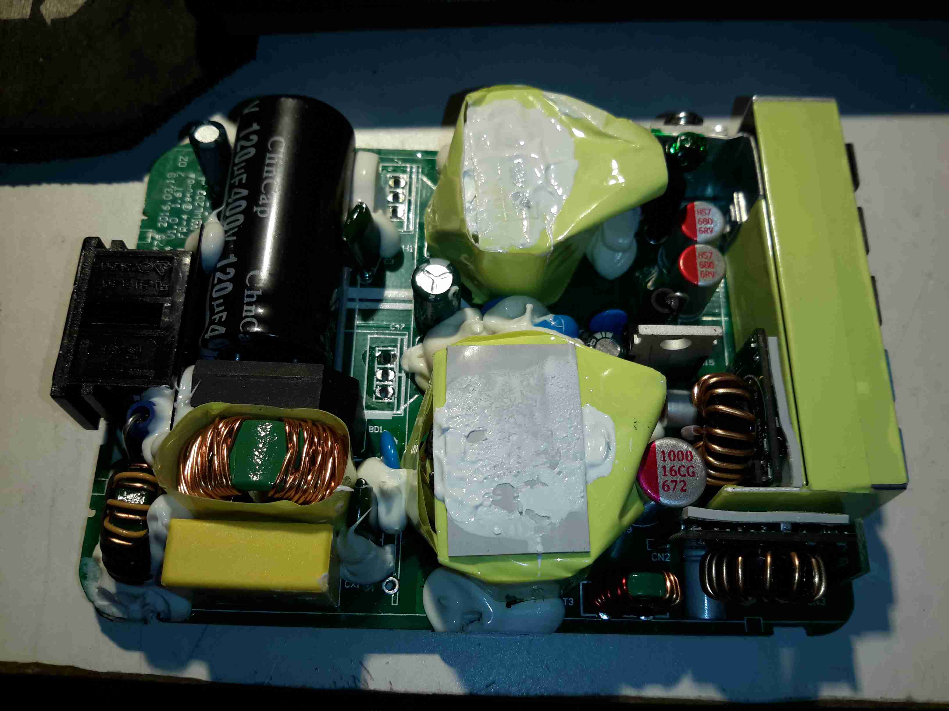
Heatsink Removed
Desoldering the pair of primary side transistors allowed me to easily remove the heatspreader from the supply. There’s thermal pads & grease over everything to get rid of the heat. Here can be seen there are two transformers, forming completely separate supplies for the standard USB side of things & the QC3 side. Measuring the voltages on the main filter capacitors showed me the difference – the QC3 supply is held at 14.2v, and is managed through other circuits further on in the power chain. There’s plenty of mains filtering on the input, as well as common-mode chokes on the DC outputs before they reach the USB ports.
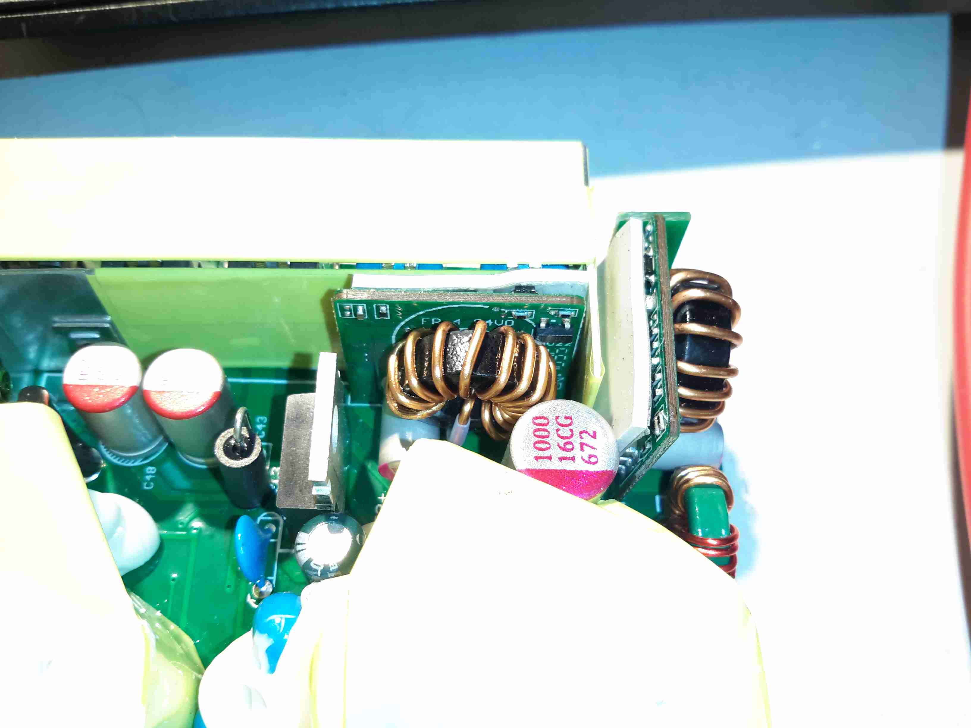
Quick Charge 3 DC-DC Converters
Here’s where the QC3 magic happens, a small DC-DC buck converter for each of the two ports. The data lines are also connected to these modules, so all the control logic is located on these too. The TO-220 device to the left is the main rectifier.
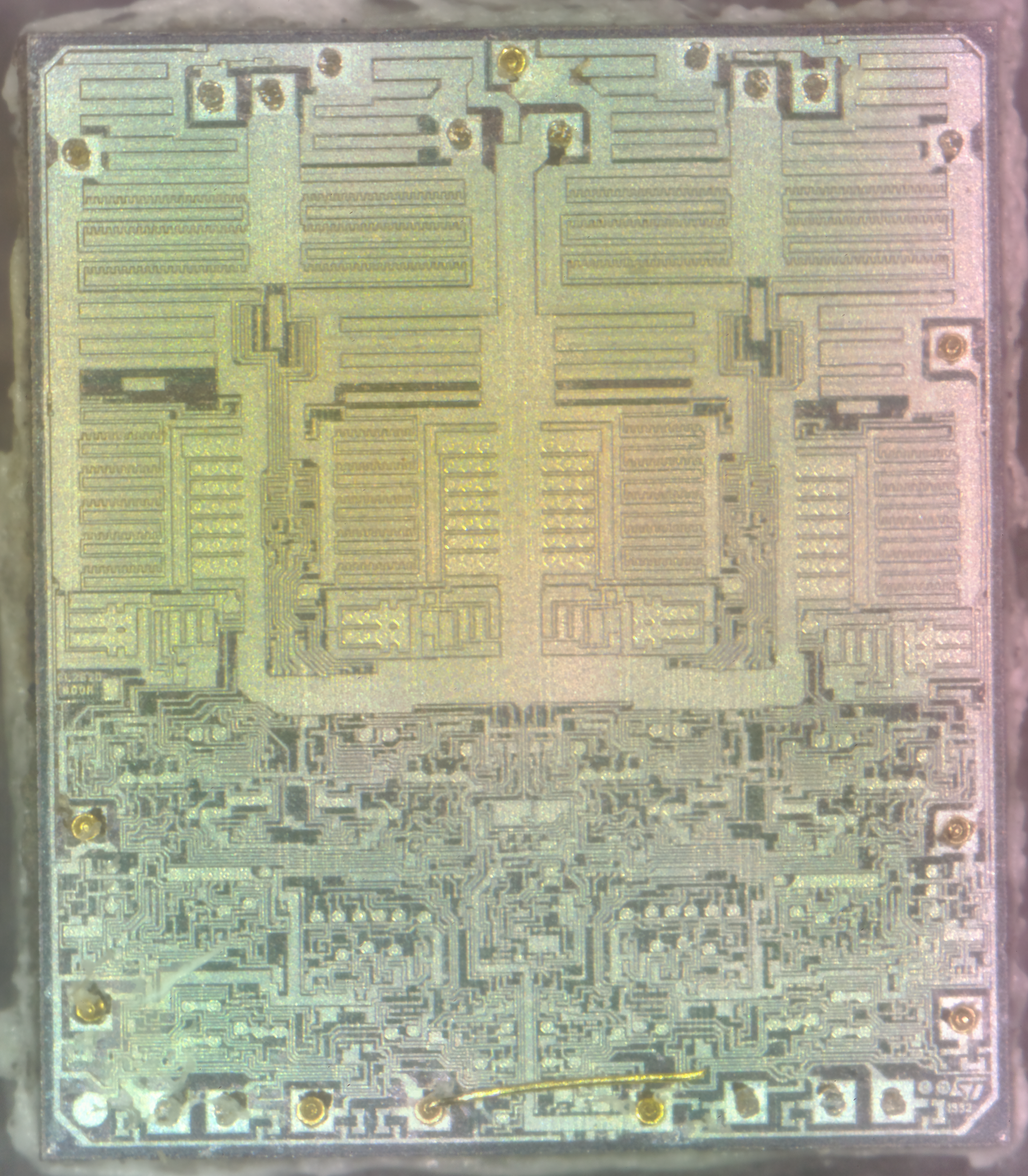
Another decapped IC! This one is an ST L6219 750mA stepper motor driver. The control logic is all at the bottom of the die, with the high current H-Bridge transistors at the top.
I wrote a few weeks ago about replacing the hot water circulating pump on the boat with a new one, and mentioned that we’d been through several pumps over the years. After every replacement, autopsy of the pump has revealed the failure mode: the first pump failed due to old age & limited life of carbon brushes. The second failed due to thermal shock from an airlock in the system causing the boiler to go a bit nuts through lack of water flow. The ceramic rotor in this one just cracked.
The last pump though, was mechanically worn, the pump bearings nicely polished down just enough to cause the rotor to stick. This is caused by sediment in the system, which comes from corrosion in the various components of the system. Radiators & skin tanks are steel, engine block cast iron, back boiler stainless steel, Webasto heat exchanger aluminium, along with various bits of copper pipe & hose tying the system together.
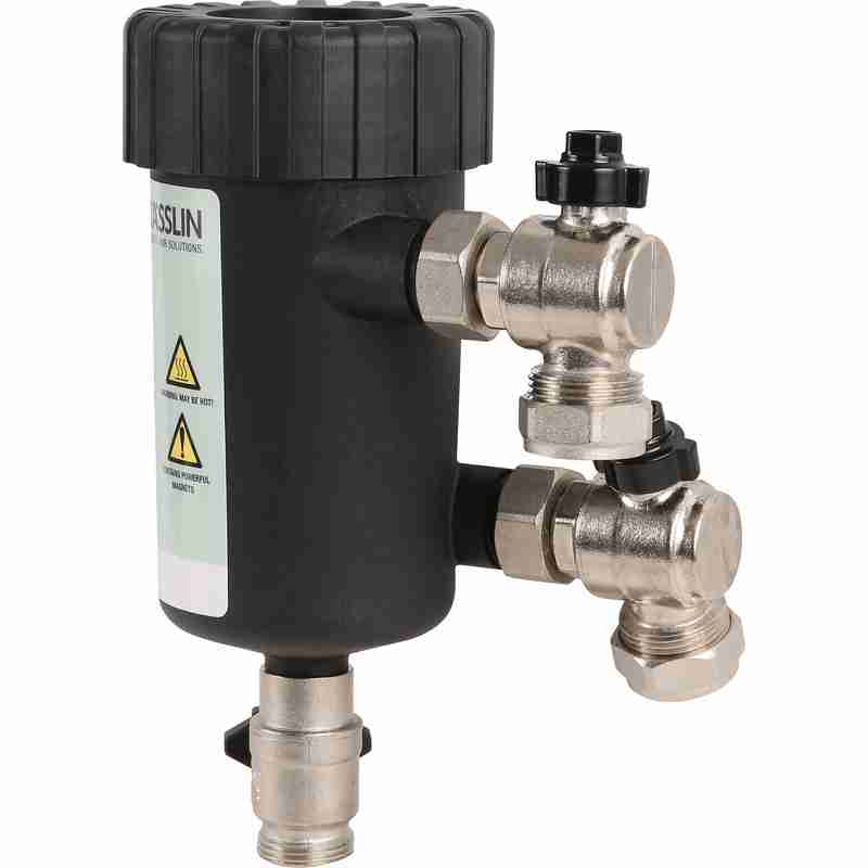
The use of dissimilar metals in a system is not particularly advisable, but in the case of the boat, it’s unavoidable. The antifreeze in the water does have anti-corrosive additives, but we were still left with the problem of all the various oxides of iron floating around the system acting like an abrasive. To solve this problem without having to go to the trouble of doing a full system flush, we fitted a magnetic filter:
Mag Filter
This is just an empty container, with a powerful NdFeB magnet inserted into the centre. As the water flows in a spiral around the magnetic core, aided by the offset pipe connections, the magnet pulls all the magnetic oxides out of the water. it’s fitted into the circuit at the last radiator, where it’s accessible for the mandatory maintenance.
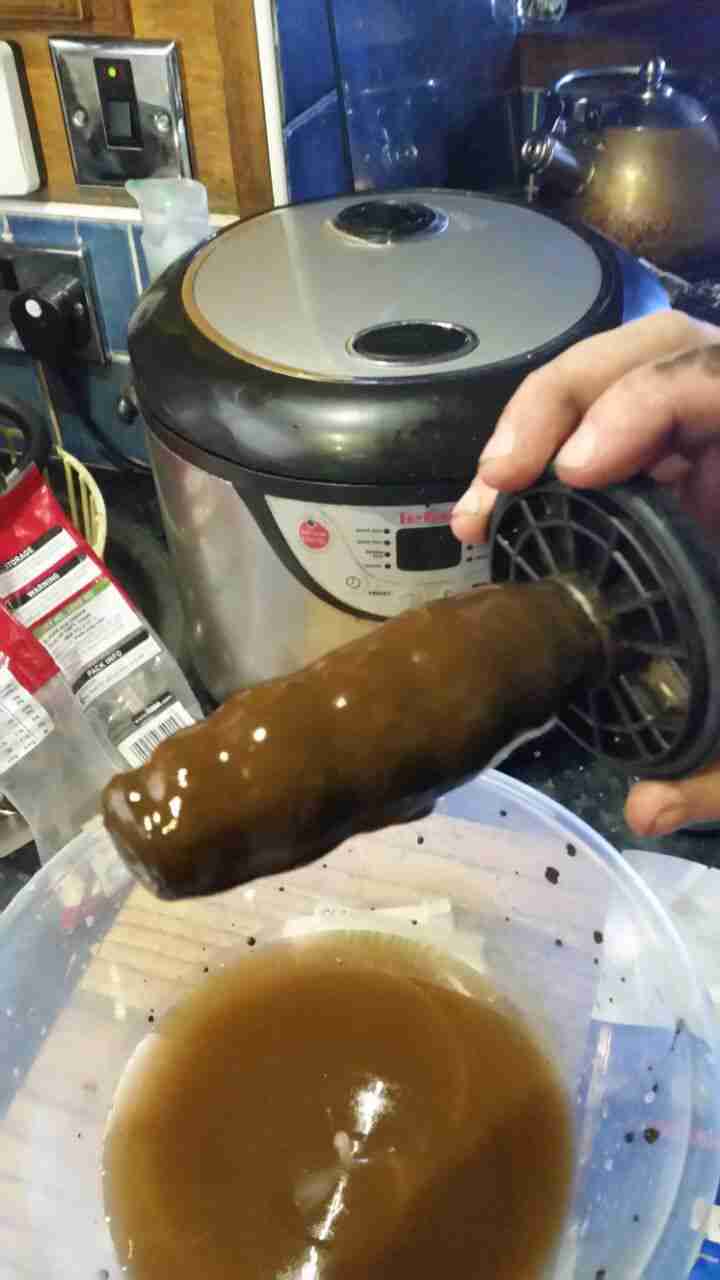
Sludge
Now the filter has been in about a month, I decided it would be a good time to see how much muck had been pulled out of the circuit. I was rather surprised to see a 1/2″ thick layer of sludge coating the magnetic core! The disgusting water in the bowl below was what drained out of the filter before the top was pulled. (The general colour of the water in the circuit isn’t this colour, I knocked some loose from the core of the filter while isolating it).
If all goes well, the level of sludge in the system will over time be reduced to a very low level, with the corrosion inhibitor helping things along. This should result in much fewer expensive pump replacements!
Tip Jar
If you’ve found my content useful, please consider leaving a donation by clicking the Tip Jar below!
All collected funds go towards new content & the costs of keeping the server online.