Posted on Leave a comment

Uniden UBC92XLT Teardown

One bit of my equipment that I’ve never looked into is my scanner, a handheld Uniden unit. I got this when Maplin Electronics had them on special offer a few years ago.

Uniden Scanner
Uniden Scanner

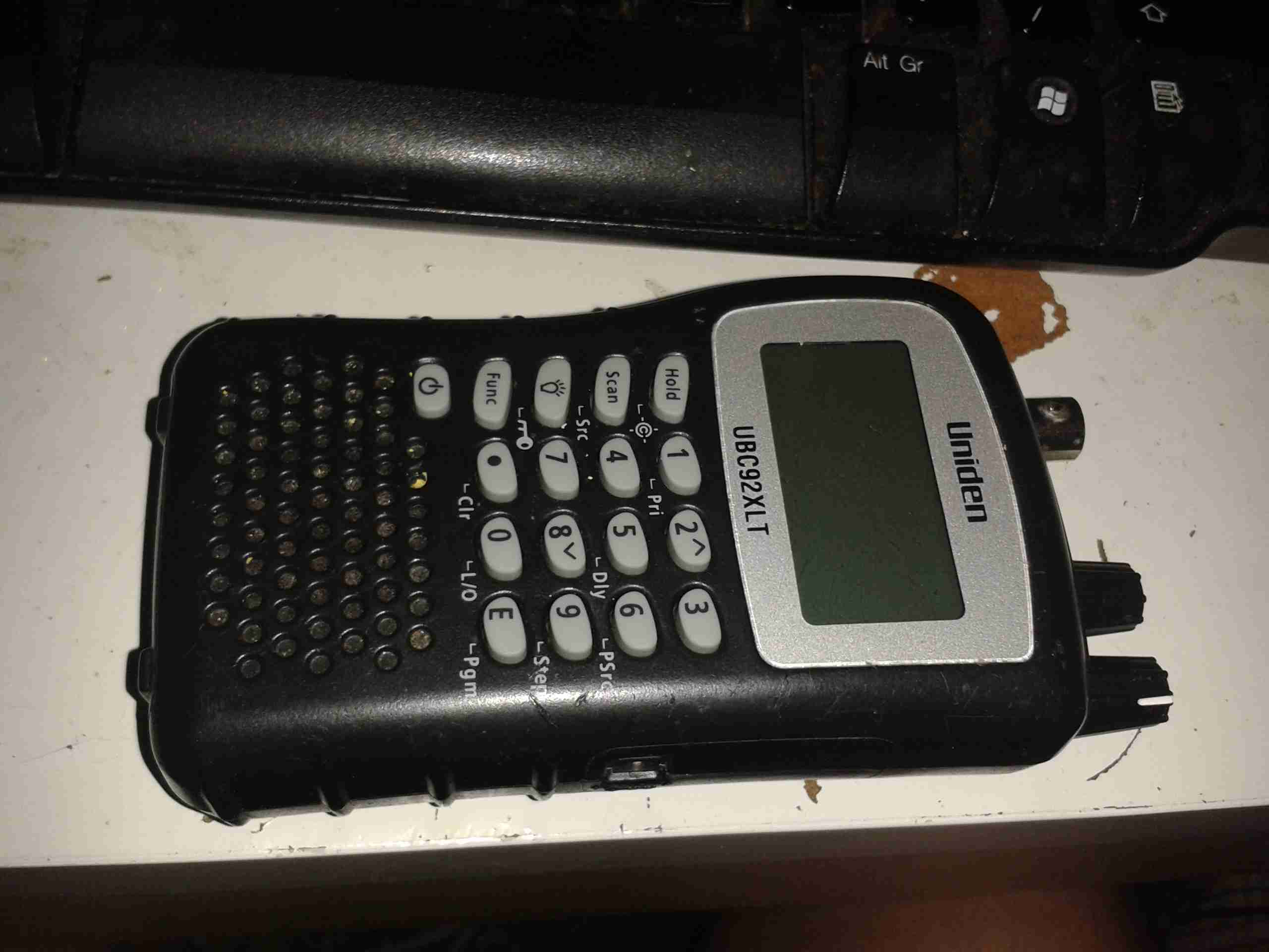
Here’s the scanner itself, roughly the same size as a usual HT.

Back Cover Removed
Back Cover Removed

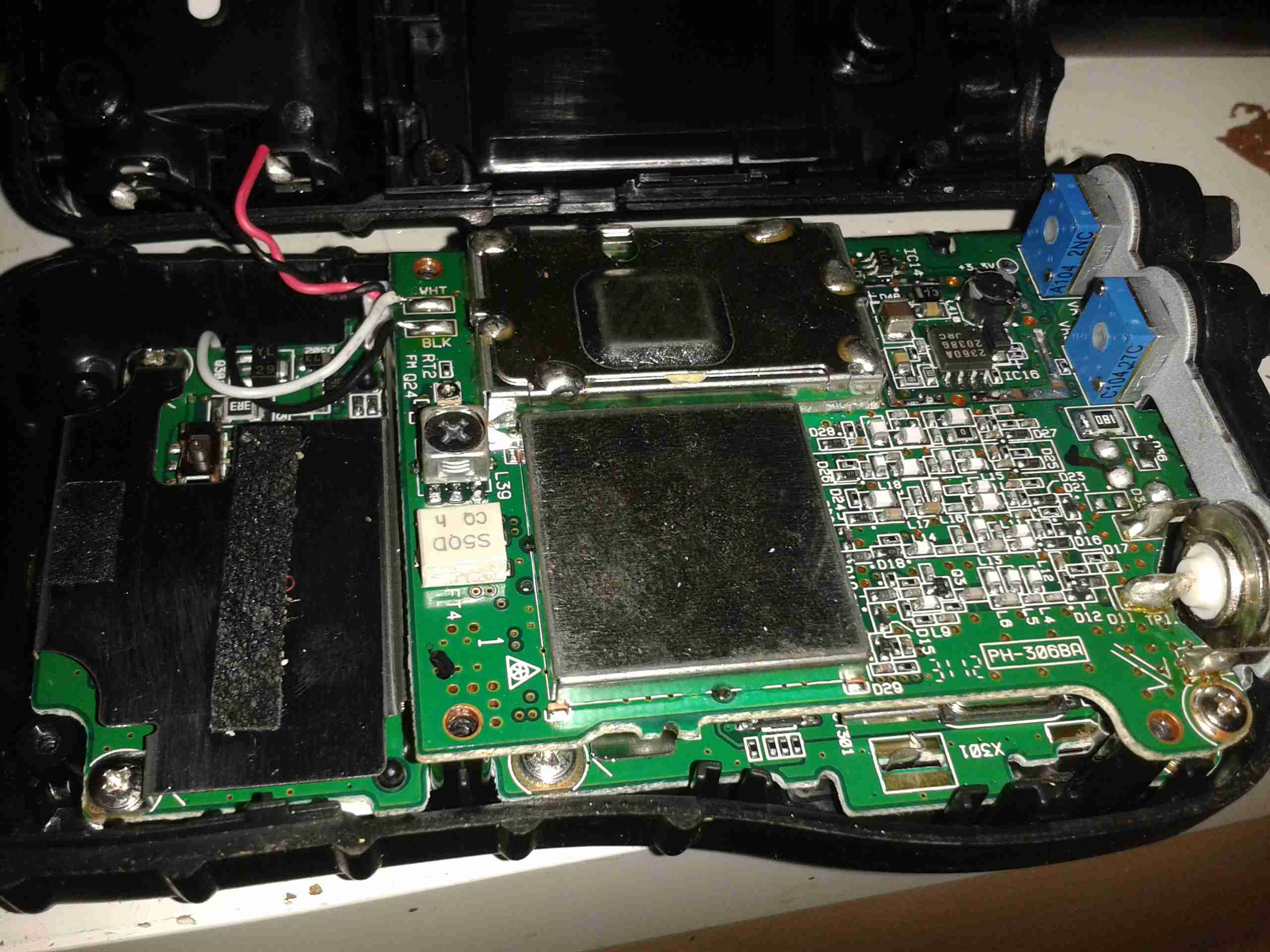
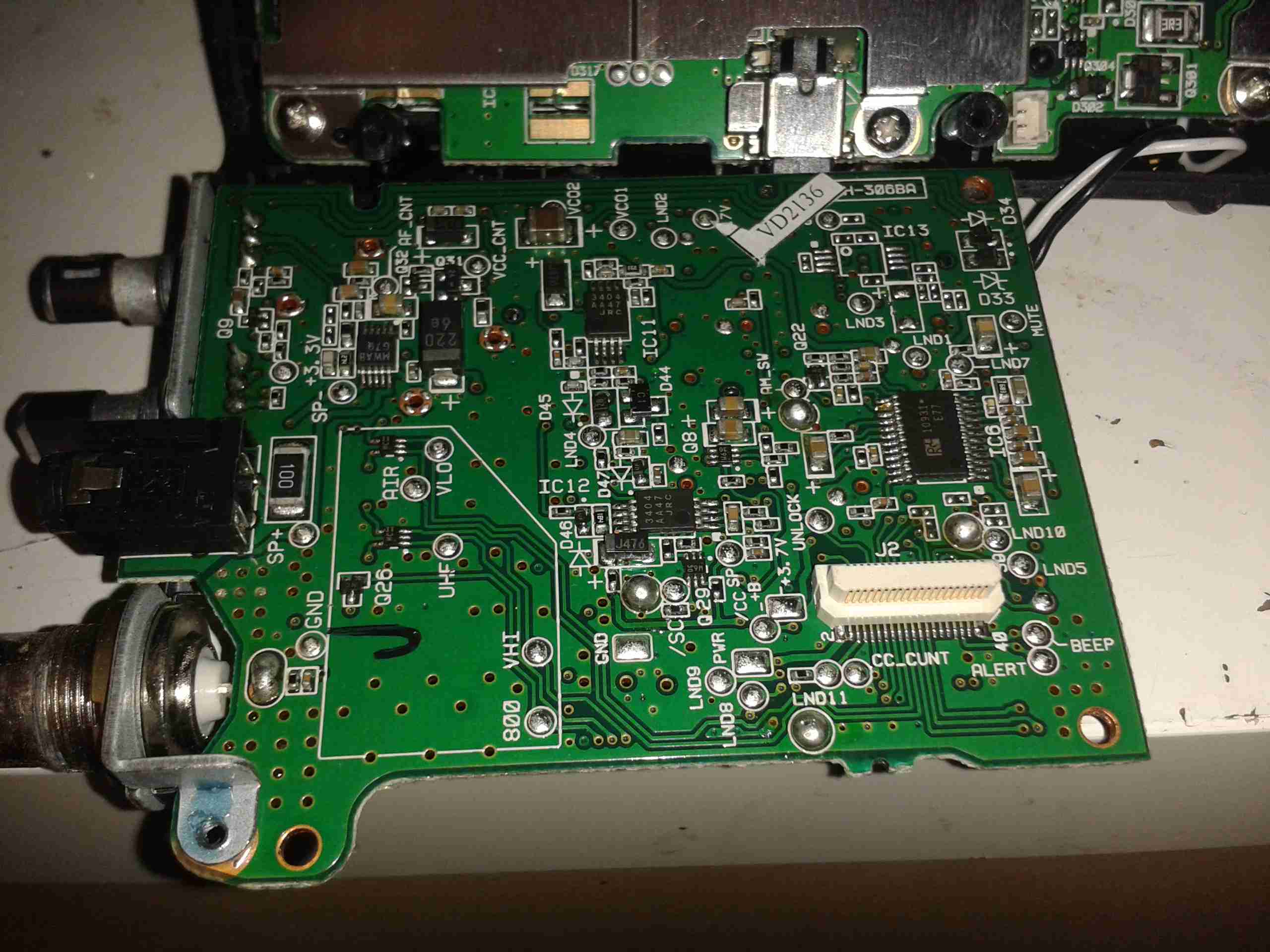
Here the back cover has been removed, and the main RF board is visible at the top of the stack. Unfortunately the shielding cans are soldered on this unit, so no looking under there 🙁
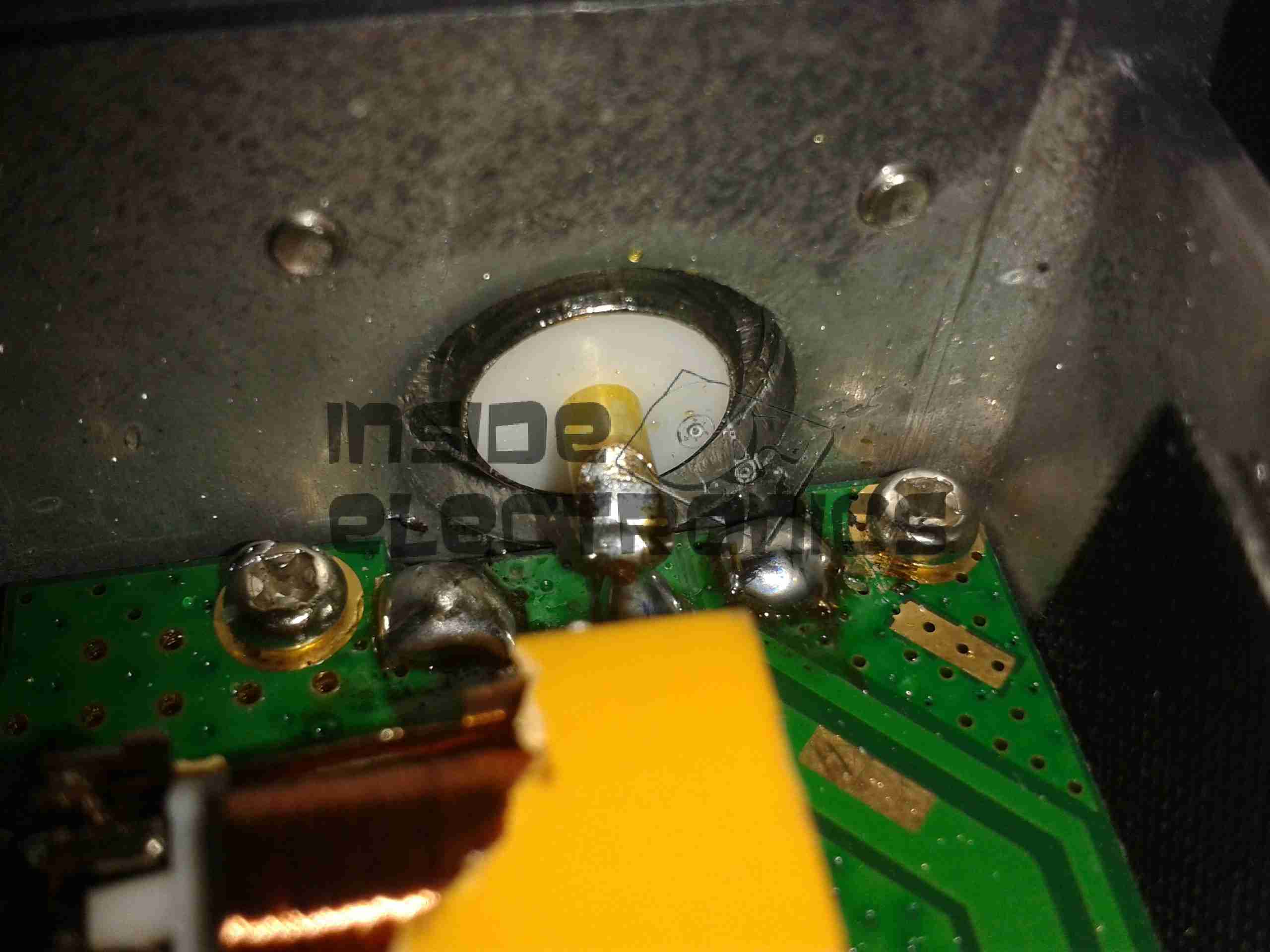
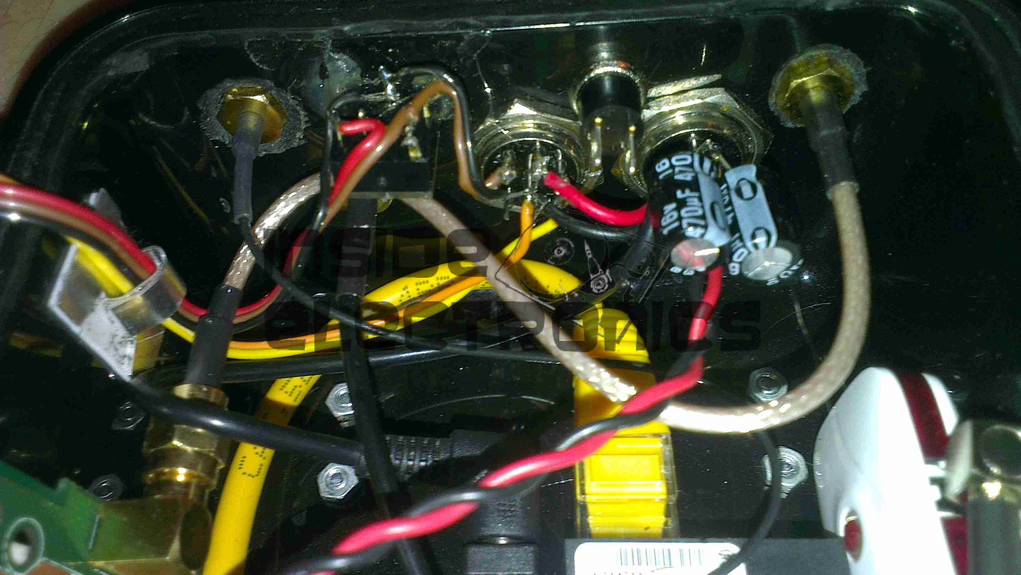
On the right hand side of the board next to the antenna input is the main RF filter network, and it’s associated switching. The RF front end is under the shield closest to the front edge.

Controls & 3.3v Regulator

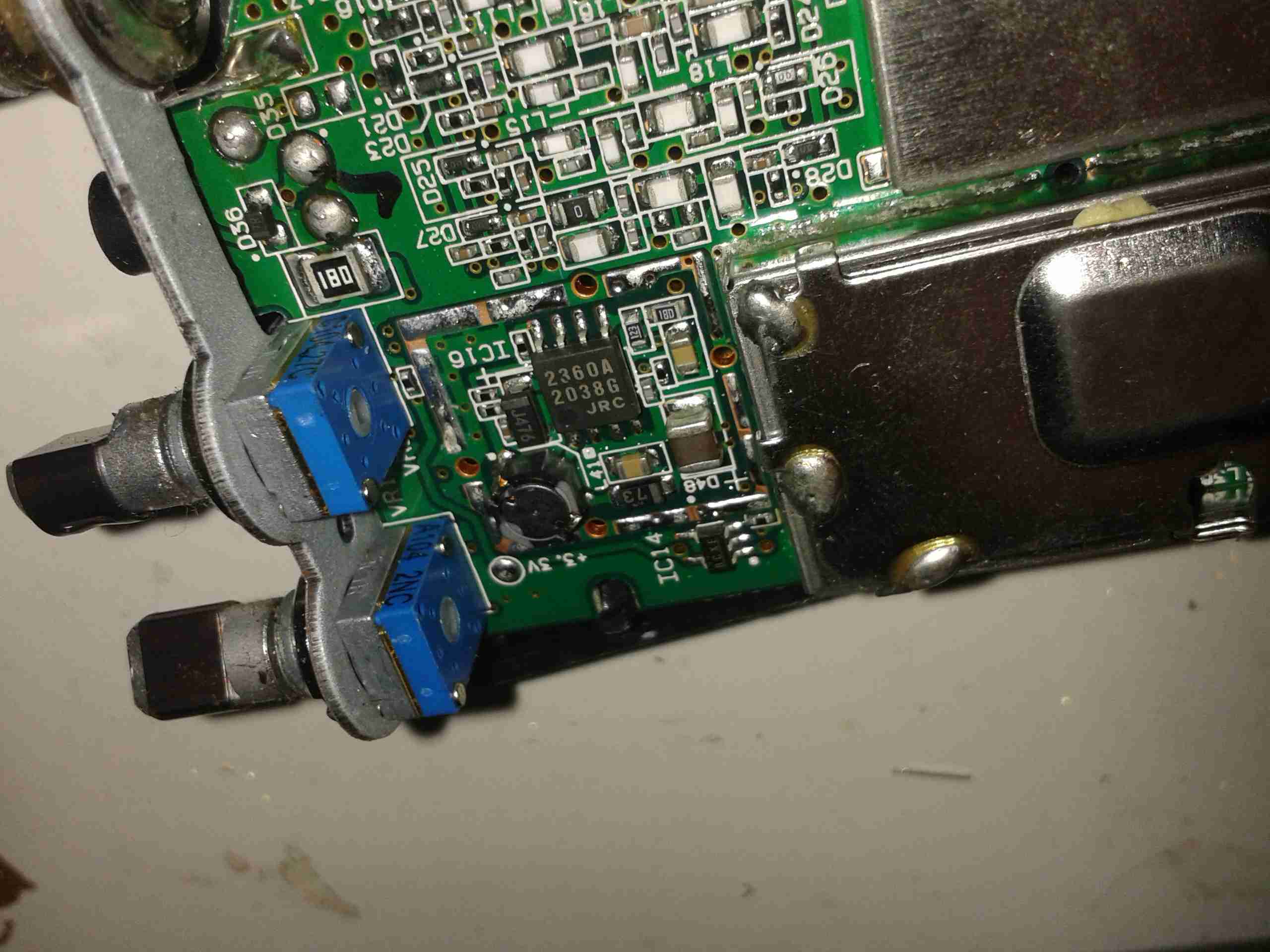
On the other side of the PCB is the Volume & Squelch potentiometers, along with a dedicated 3.3v switching supply. An NJM2360A High Precision DC/DC converter IC controls this one. A 3.3v test point is visible next to the regulator.

RF Board Reverse
RF Board Reverse

Here’s the backside of the RF board, some more interesting parts here. There’s a pair of NJM3404A Single Supply Dual Op-Amp ICs, and a TK10931V Dual AM/FM IF Discriminator IC. This is the one that does all the back-end radio functionality. The audio amplifier for the internal speaker & external headphone jack is also on this PCB, top left. A board-to-board interconnect links this radio board with the main control board underneath.

Control PCB Front
Control PCB Front

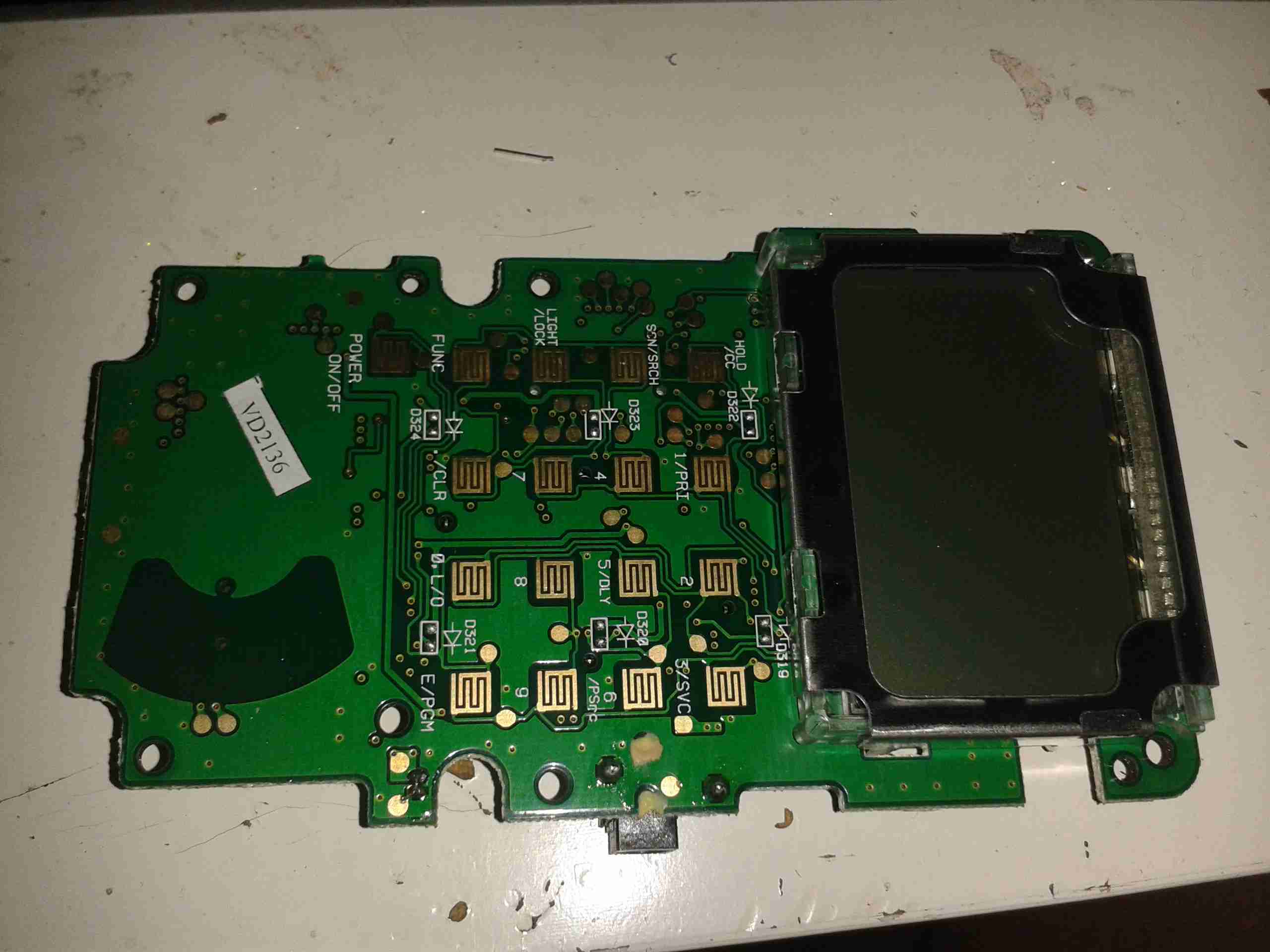
Here’s the front of the control PCB, nothing much to see here, just the LCD & membrane keypad contacts.

Control PCB Reverse
Control PCB Reverse

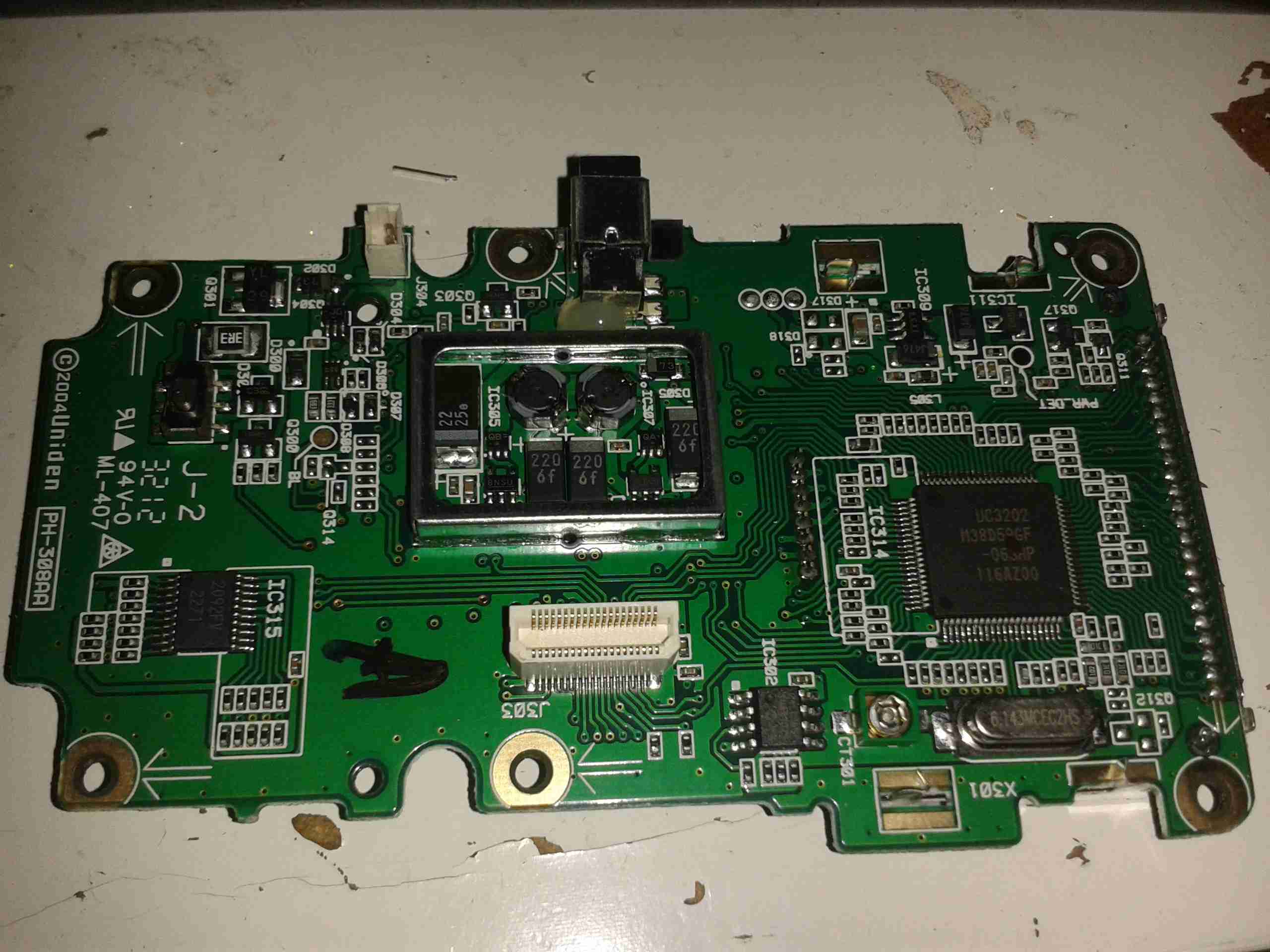
And here’s the reverse side of the control board. All the interesting bits are here. The main microcontroller is on the right, a Renesas M38D59GF, a fairly powerful MCU, with onboard LCD drive, A/D converter, serial interface, 60K of ROM & 2K of RAM. It’s 6.143MHz clock crystal is just below it.
The mating connector for the RF board is in the centre here.

There is also a Microchip 24LC168 16KB I²C EEPROM next to the main microcontroller. This is probably for storing user settings, frequencies, etc.

EEPROM
EEPROM

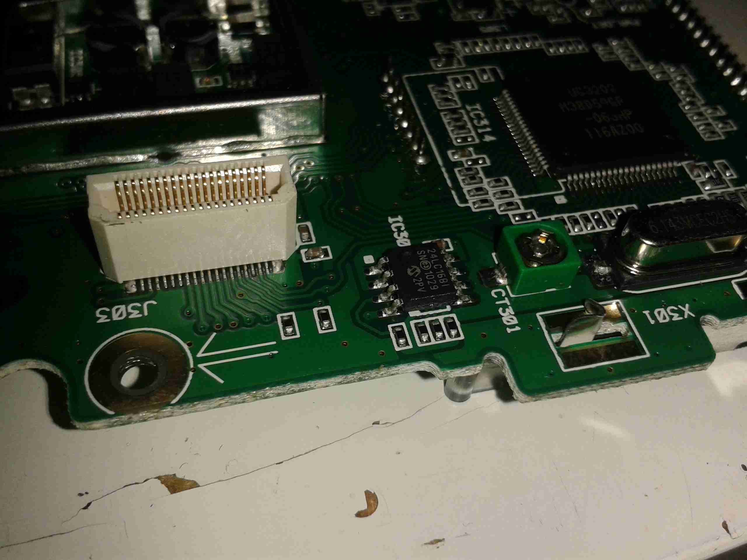
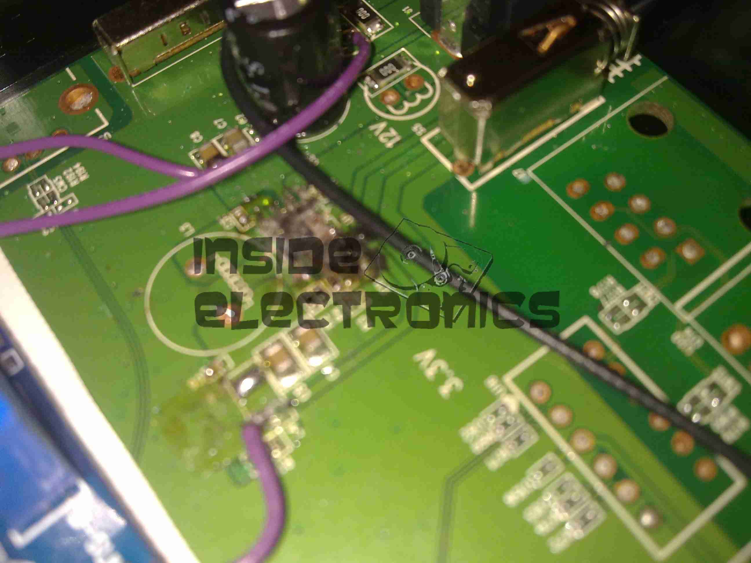
The rest of this board is dedicated to battery charging and power supply, in the centre is a dual switching controller, I can’t figure out the numbers on the tiny SOT23 components in here, but this is dealing with the DC 6v input & to the left of that is the circuitry for charging the NiMH cells included with the scanner.

PSU
PSU

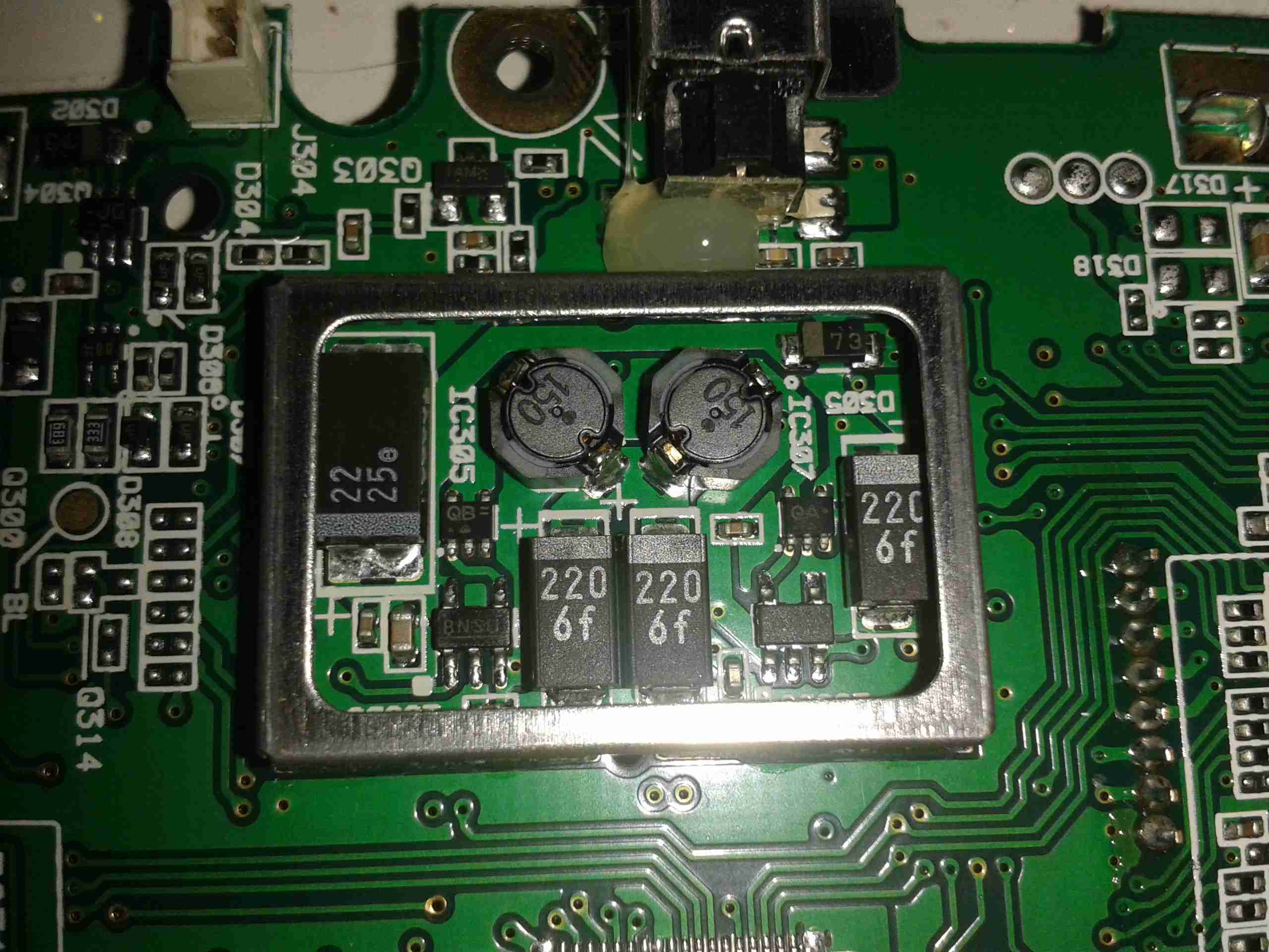
The last bit of this PCB is a BU2092FV Serial In / Parallel Out 4 channel driver. Not sure what this one is doing, it might be doing some signal multiplexing for the RF board interface. Unfortunately the tracks from this IC are routed on the inner layers of the board so they can’t be traced out.

Posted on Leave a comment

Wouxun KG-UV950P Teardown & Analysis

Following on from my review, here are some internal views & detail on the components used in this radio. Below is an overview of the main PCB with the top plate removed from the radio.

Cover Removed
Cover Removed
RF Final Amplifier Stage

Most visible are these MOSFETs, which are Mitsubishi RD70HVF1 VHF/UHF power devices.  Rated for a maximum of 75W output power at 12.5v (absolute maximum of 150W, these are used well within their power ratings. They are joined to the PCB with heavy soldering, with bypass caps tacked right on to the leads.

RF Pre Drivers
RF Pre Drivers

Here is the RF pre-driver stage, with intermediate transistors hidden under the small brass heatspreader.

Power Section
Power Section

In the top left corner of the radio, near the power input leads, is the power supply & audio amplifier section. Clearly visible are the pair of LA4425A 5W audio power amplifier ICs, these drive the speakers on the top of the radio. Either side of these parts are a 7809 & a 7805 – both linear regulators providing +9v & +5v logic supplies respectively. The large TO220 package device is a KIA378R08PI 3A LDO regulator with ON/OFF control, this one outputs +8v. Just visible in the top right corner are the sockets for the speaker connections.

DTMF Circuits
DTMF Circuits

Here are the two ICs for dealing with DTMF tones, they are HM9170 receivers.

Glue Logic
Glue Logic

In the corner next to the interface jack, there are some CD4066B Quad Bilateral switches. These make sense since the interface jack has more than a single purpose, these will switch signals depending on what is connected.

RF Section
RF Section

Here are visible the RF cans for the oscillators, the crystals visible next to the can at the top. The shields are soldered on, so no opening these unfortunately.
Also visible in this image is a CMX138A Audio Scrambler & Sub-Audio Signalling processor. This IC deals with the Voice Inversion Scrambling feature of the radio, & processes the incoming audio before being sent to the modulator.

Output Filter Network

Shown here is the RF output filter network, this radio uses relays for switching instead of PIN diodes, I imagine for cost reasons. The relay closest to the RF output socket has had a slight accident 🙂 This is slated to be replaced soon.

RF Output Jack
RF Output Jack

Finally, the RF output jack.

Audio Speakers
Audio Speakers

Here the speakers are shown, attached to the bottom of the top plate. They are both rated 8Ω 1W.

Posted on Leave a comment

ZyXel WAP3205 Repair

Here is a ZyXel WAP3205 WiFi Access Point that has suffered a reverse polarity event, due to an incorrect power supply being used with the unit.

ZyXEL WAP3205
ZyXEL WAP3205

While most electronic gadgets are protected against reverse polarity with a blocking diode, this unit certainly wasn’t. Applying +12v DC the wrong way round resulted in this:

Blown Switchmode IC
Blown Switchmode IC (Fuzzy Focus)

That is the remains of the 3.3v regulator IC, blown to smithereens & it even attempted an arson attack. Luckily this was the only damaged component, & I was able to repair the unit by replacing the switching IC with a standalone regulator. (Replacing the IC would have been preferable, if there was anything left of it to obtain a part number from).

I scraped away the pins of the IC to clear the short on the input supply, removed the switching inductor, & tacked on an adjustable regulator module set to 3.3v. Luckily the voltage of the supply is handily marked on the PCB next to the circuit.

Replacement PSU
Replacement PSU

Replacement SMPS in place on top of the PCB. The output of the supply is connected to one of the pads of L4 (on my unit just an 0 ohm link), the +12v input is connected to the + rail side of C8 & C7 & the final ground connection is hooked in to the back of the barrel jack.

After this replacement, the unit booted straight up as if nothing had happened. All the logic is undamaged!

Makerplate
Makerplate
Posted on Leave a comment

Marine Potable Water Management System

LCD Panel
LCD Panel

Having two separate water tanks on nb Tanya Louise, with individual pumps, meant that monitoring water levels in tanks & keeping them topped up without emptying & having to reprime pumps every time was a hassle.
To this end I have designed & built this device, to monitor water usage from the individual tanks & automatically switch over when the tank in use nears empty, alerting the user in the process so the empty tanks can be refilled.

Based around an ATMega328, the unit reads a pair of sensors, fitted into the suction line of each pump from the tanks. The calculated flow is displayed on the 20×4 LCD, & logged to EEPROM, in case of power failure.

Water Flow Sensor
Water Flow Sensor

When the tank in use reaches a preset number of litres flowed, (currently hardcoded, but user input will be implemented soon), the pump is disabled & the other tank pump is enabled. This is also indicated on the display by the arrow to the left of the flow register. Tank switching is alerted by the built in beeper.
It is also possible to manually select a tank to use, & disable automatic operation.
Resetting the individual tank registers is done by a pair of pushbuttons, the total flow register is non-resettable, unless a hard reset is performed to clear the onboard EEPROM.

Main PCB
Main PCB

View of the main PCB is above, with the central Arduino Pro Mini module hosting the backend code. 12-24v power input, sensor input & 5v sensor power output is on the connectors on the left, while the pair of pump outputs is on the bottom right, switched by a pair of IRFZ44N logic-level MOSFETS. Onboard 5v power for the logic is provided by the LM7805 top right.

Code & PCB design is still under development, but I will most likely post the design files & Arduino sketch once some more polishing has been done.

Posted on Leave a comment

Datakom DKG-171

Front
Front

Here is a teardown of the Datakom DKG-171 generator transfer controller. Here is the front of the unit, with the pictogram of the system, the indicator LEDs & the generator test button.


Rear
Rear

The rear of the unit features the connection points for the mains, generator & generator control I/O.

PCB Rear
PCB Rear

Rear of the PCB with the control relays. The two larger relays switch in the remote contactors to switch the mains supply over between the grid & the generator, while the smaller relay switches 12v power out to a terminal to automatically start the generator.

PCB Front
PCB Front

Front of the PCB with the control logic & main PIC microcontroller.


Posted on Leave a comment

Solar Cable Upgrade & Pseudo-MPPT

New Cable
New Cable

As the cable supplied with the panel is far too short, inflexible & does not even allow the cable gland on the terminal box to form a seal, I have replaced it with some high quality twin core guitar cable, with silicone insulation.

The cable is removable from the panel tail by means of a screwlock two pin connector.


On another note, I have noticed a side effect of fitting a switchmode regulator to the panel: it seems to have formed an MPPT-type regulator setup, as even in low light conditions, when the bare panel is outputting 18.5v at 50mA short circuit, with the switching regulator I can get a useable 13.25v at ~170mA.
This effect is increased in full light, where I can obtain 4.5A short circuit current & ~1.8A at 13.25v output.

Posted on Leave a comment

Wearable Raspberry Pi – Some Adjustments

USB Hub
USB Hub

As the first USB hub I was using was certainly not stable – it would not enumerate between boots & to get it working again would require waiting around 12 hours before applying power, it has been replaced. This is a cheapie eBay USB hub, of the type shown below.

These hubs are fantastic for hobbyists, as the connections for power & data are broken out on the internal PCB into a very convenient row of pads, perfect for integration into many projects.

Breakout Hub
Breakout Hub

I now have two internal spare USB ports, for the inbuilt keyboard/mouse receiver & the GPS receiver I plan to integrate into the build.

These hubs are also made in 7-port versions, however I am not sure if these have the same kind of breakout board internally. As they have the same cable layout, I would assume so.


Connector Panel
Connector Panel

Here is a closeup of the back of the connectors, showing a couple of additions.

I have added a pair of 470µF capacitors across the power rails, to further smooth out the ripple in the switching power supply, as I was having noise issues on the display.

Also, there is a new reset button added between the main interface connectors, which will be wired into the pair of pads that the Raspberry Pi has to reset the CPU.
This can be used as a power switch in the event the Pi is powered down when not in use & also to reset the unit if it becomes unresponsive.


Posted on Leave a comment

Hot Laminator

Top
Top

Here is a cheap no brand hot laminator. This pulls the paper, inside a plastic pouch through a pair of heated rollers to seal it.

Heater
Heater

Top removed, heater assembly visible. PCB attached to the top cover holds LEDs to indicate power & ready status.

Switch
Switch
Thermostat
Thermostat

Here is the thermostat & thermal fuse, the thermostat switching the indicator on the front panel to tell the user when the unit is up to temperature. This has a self regulating thermostat. Thermal fuse inside the heat resistant tubing is to protect against any failure of the heater.

Motor
Motor

5 RPM motor that turns the rollers through a simple gear system.

Posted on Leave a comment

Power Pack Regulator Update

7.5v Regulator
7.5v Regulator

To help make my system more efficient, a pair of switching regulators has been fitted, the one shown above is a Texas Instruments PTN78060 switchmode regulator module, which provides a 7.5v rail from the main 12v battery pack.

A Lot like the LM317 & similar linear regulators, these modules require a single program resistor to set the output voltage, but are much more efficient, around the 94% mark at the settings used here.

The 7.5v rail supplies the LM317 constant current circuit in the laser diode driver subsection. This increases efficiency by taking some voltage drop away from the LM317.

5v Regulator
5v Regulator

The 7.5v rail also provides power to this Texas Instruments  PTH08000 switchmode regulator module, providing the 5v rail for the USB port power.

Posted on Leave a comment

Chicom “500W” ATX PSU

Cover Removed
Cover Removed

Here is a cheapo 500W rated ATX PSU that has totally borked itself, probably due to the unit NOT actually being capable of 500W. All 3 of the switching transistors were shorted, causing the ensuing carnage:

AC Input
AC Input

Here is the AC input to the PCB. Note the vapourised element inside the input fuse on the left. There is no PFC/filtering built into this supply, being as cheap as it is links have been installed in place of the RFI chokes.

Input Side
Input Side

Main filter capacitors & bridge rectifier diodes. PCB shows signs of excessive heating.

Filter Caps Removed
Filter Caps Removed

Filter capacitors have been removed from the PCB here, showing some cooked components. Resistor & diode next to the heatsink are the in the biasing network for the main switching transistors.

Heatsinks Removed
Heatsinks Removed

Heatsink has been removed, note the remaining pin from one of the switching transistors still attached to the PCB & not the transistor 🙂

Transformers
Transformers

Output side of the PSU, with heatsink removed. Main transformer on  the right, transformers centre & left are the 5vSB  transformer & feedback transformer.

Output Side
Output Side

Output side of the unit, filter capacitors, choke & rectifier diodes are visible here attached to their heatsink.

Comparator
Comparator

Comparator IC that deals with regulation of the outputs & overvoltage protection.