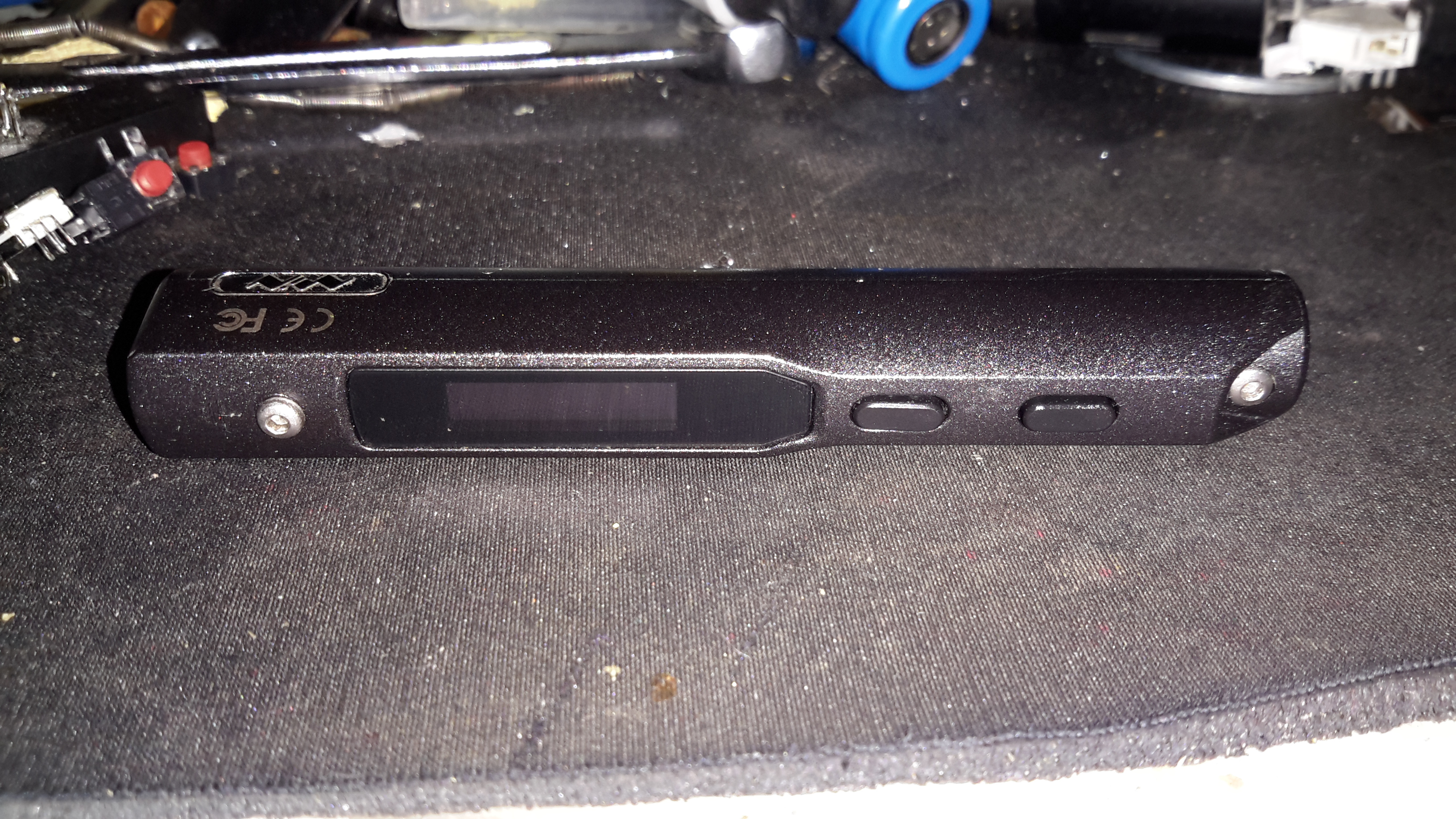
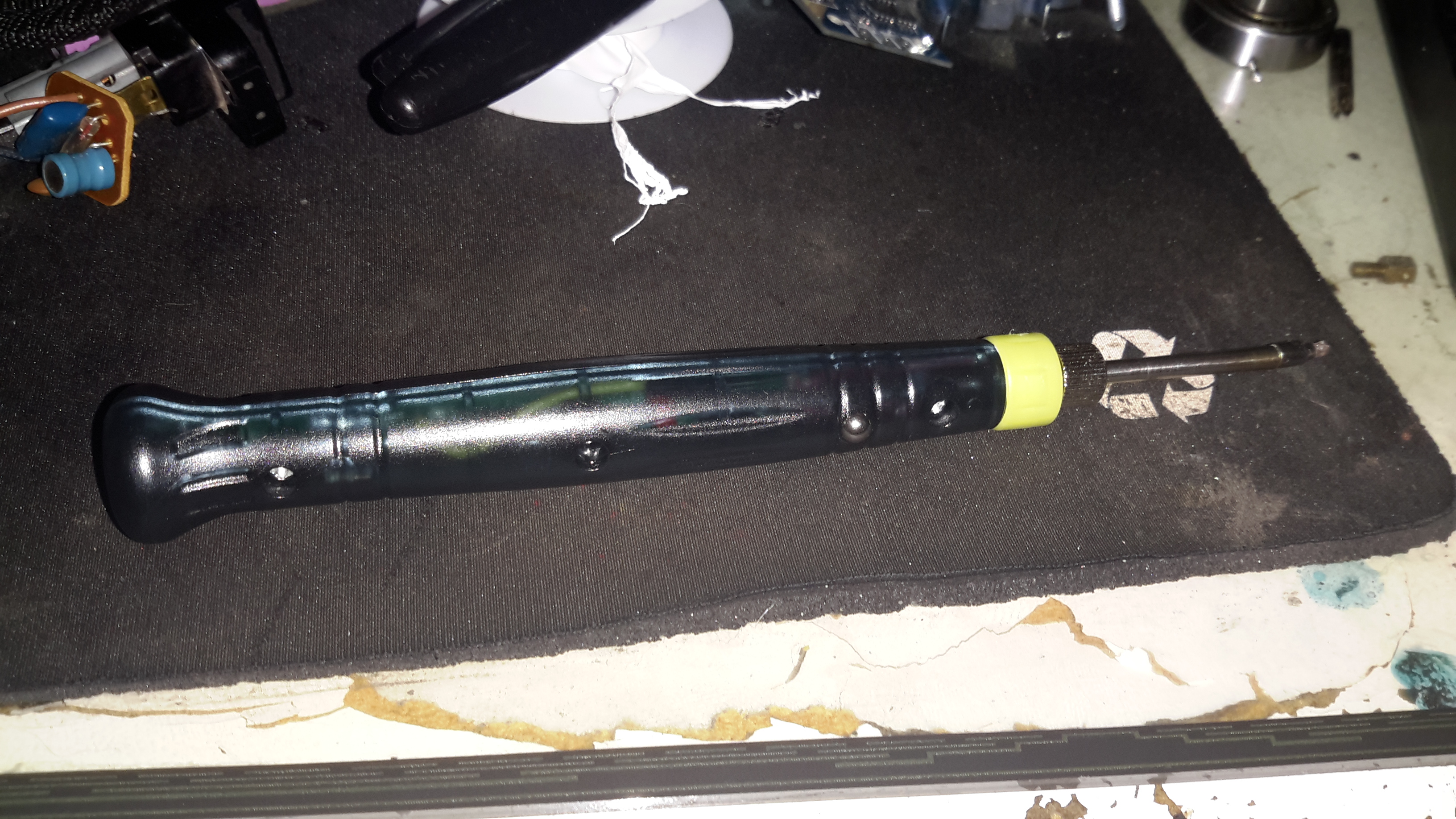
When I ordered the tiny USB soldering iron, I decided a proper iron upgrade would be a good idea. Looking around for something that didn’t require AC mains power turned up the TS100, a Chinese design, that unusually is actually very good! Above is the handle itself, with it’s small OLED display & two operation buttons.
This iron is controlled by a STM32 ARM microcontroller, the firmware & schematics are completely open-source.
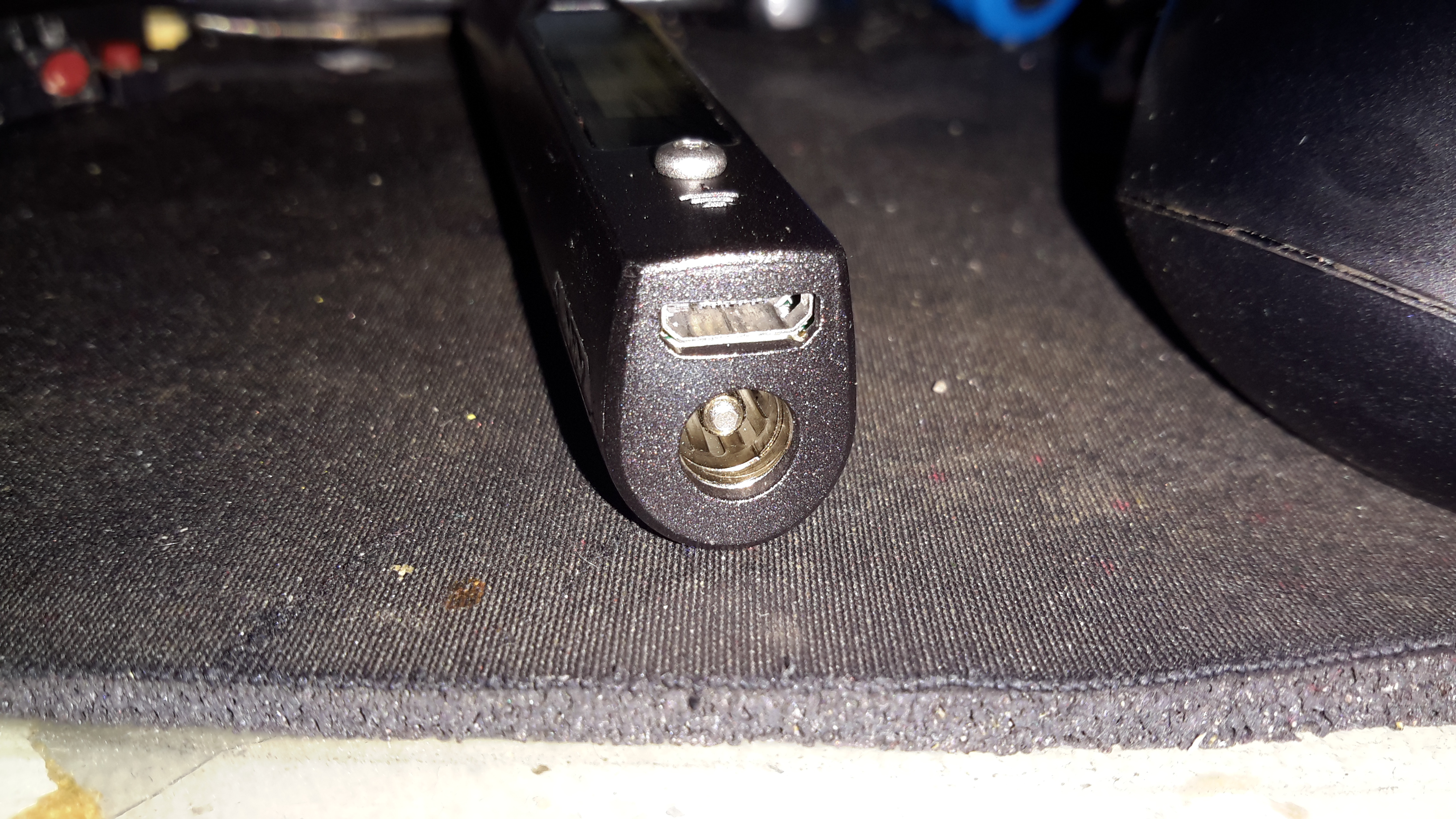
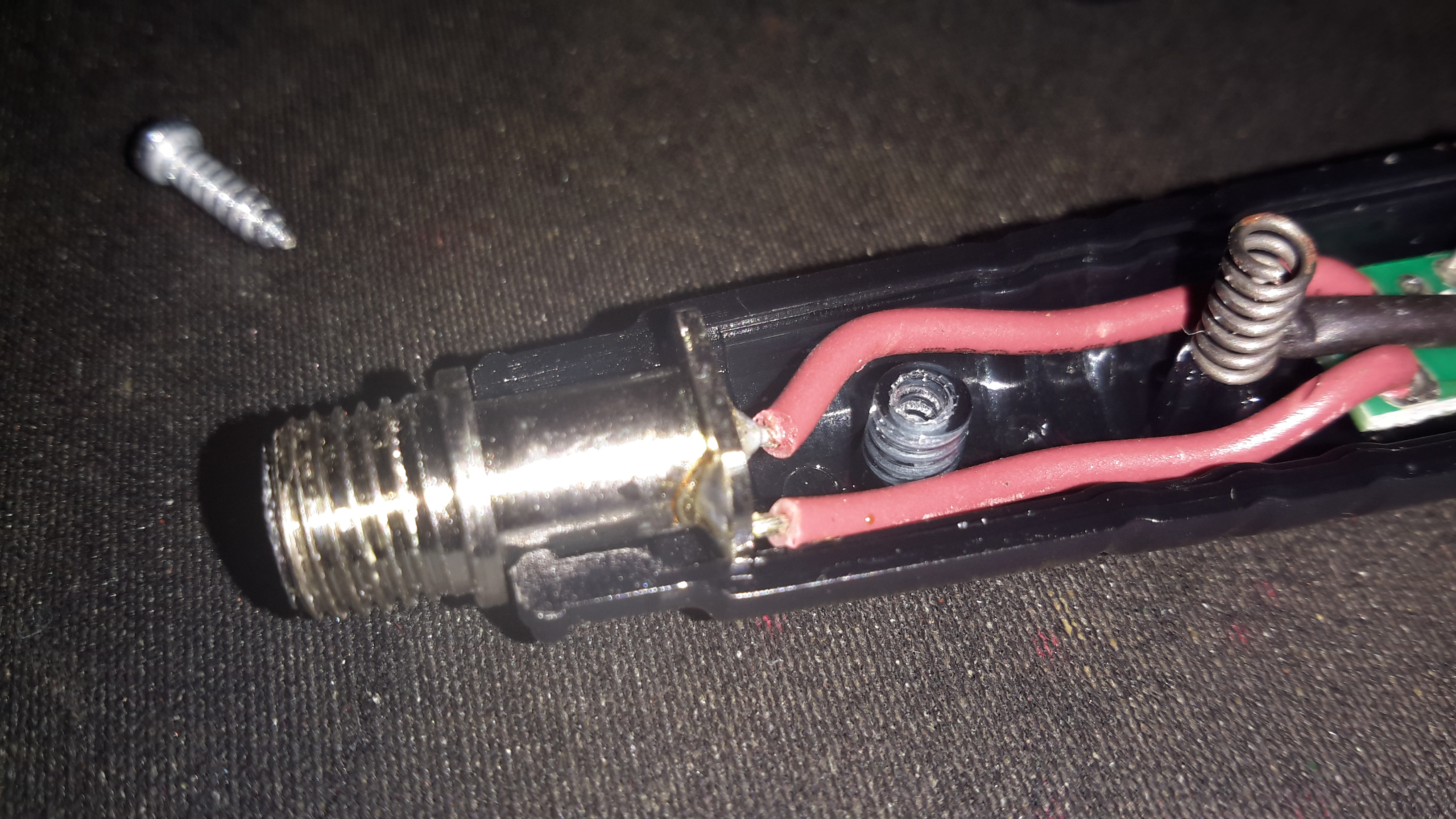
DC Input Jack / USB Port
The bottom end of the iron has the main DC input jack, designed with laptop chargers in mind (DC input range from 10v-24v). Above that is the micro USB port for programming.
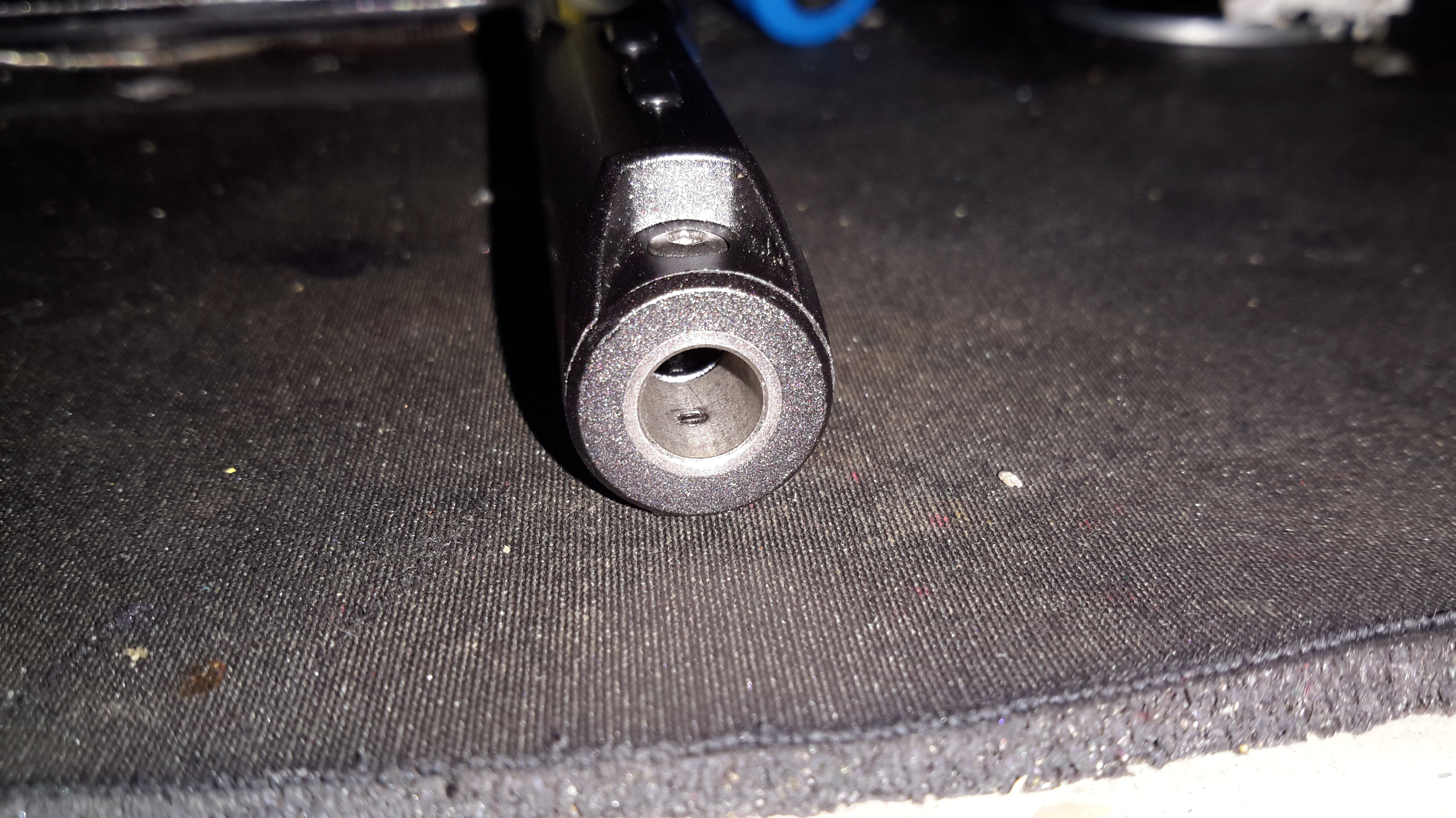
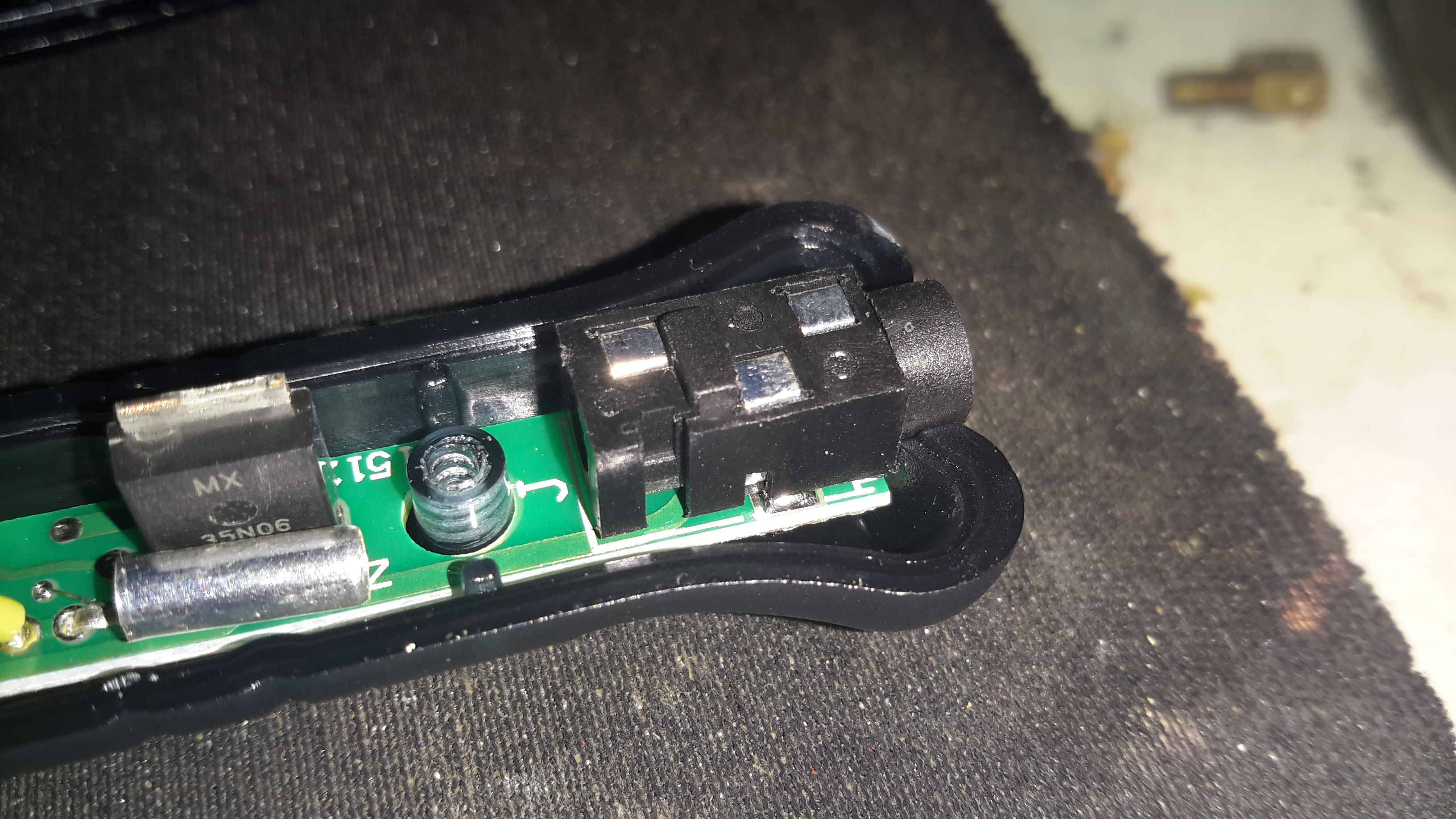
Heating Element Socket
The iron tips slot into the other end, many different tip types & shapes are available. The one supplied was the simple conical tip.
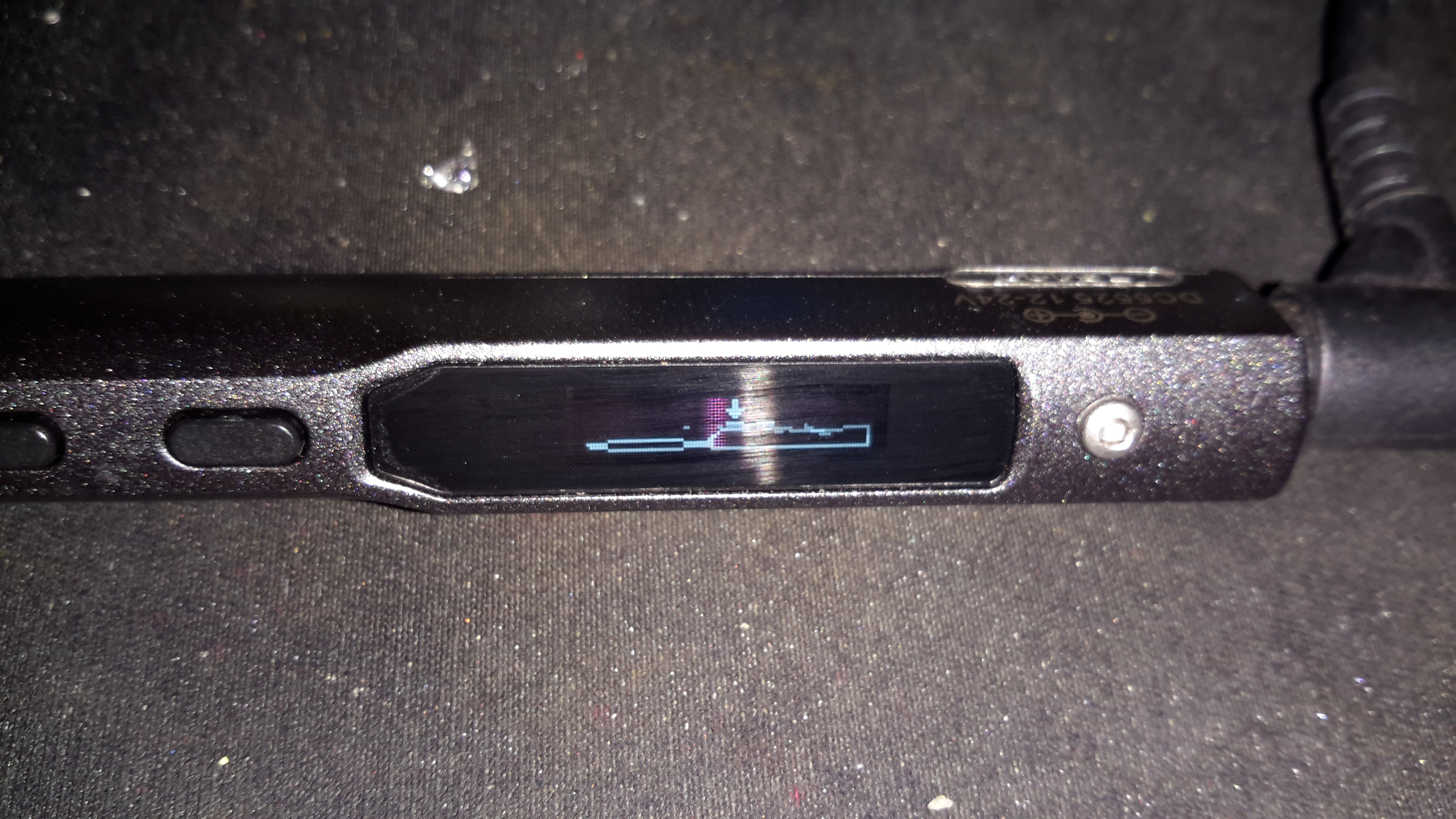
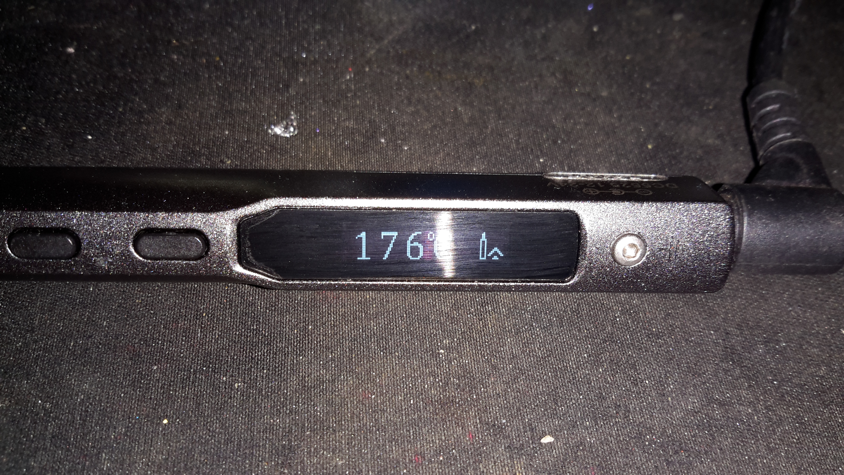
Standby Screen
Plugging the iron into some power gets a standby screen – it doesn’t just start heating immediately, for safety.
Heating
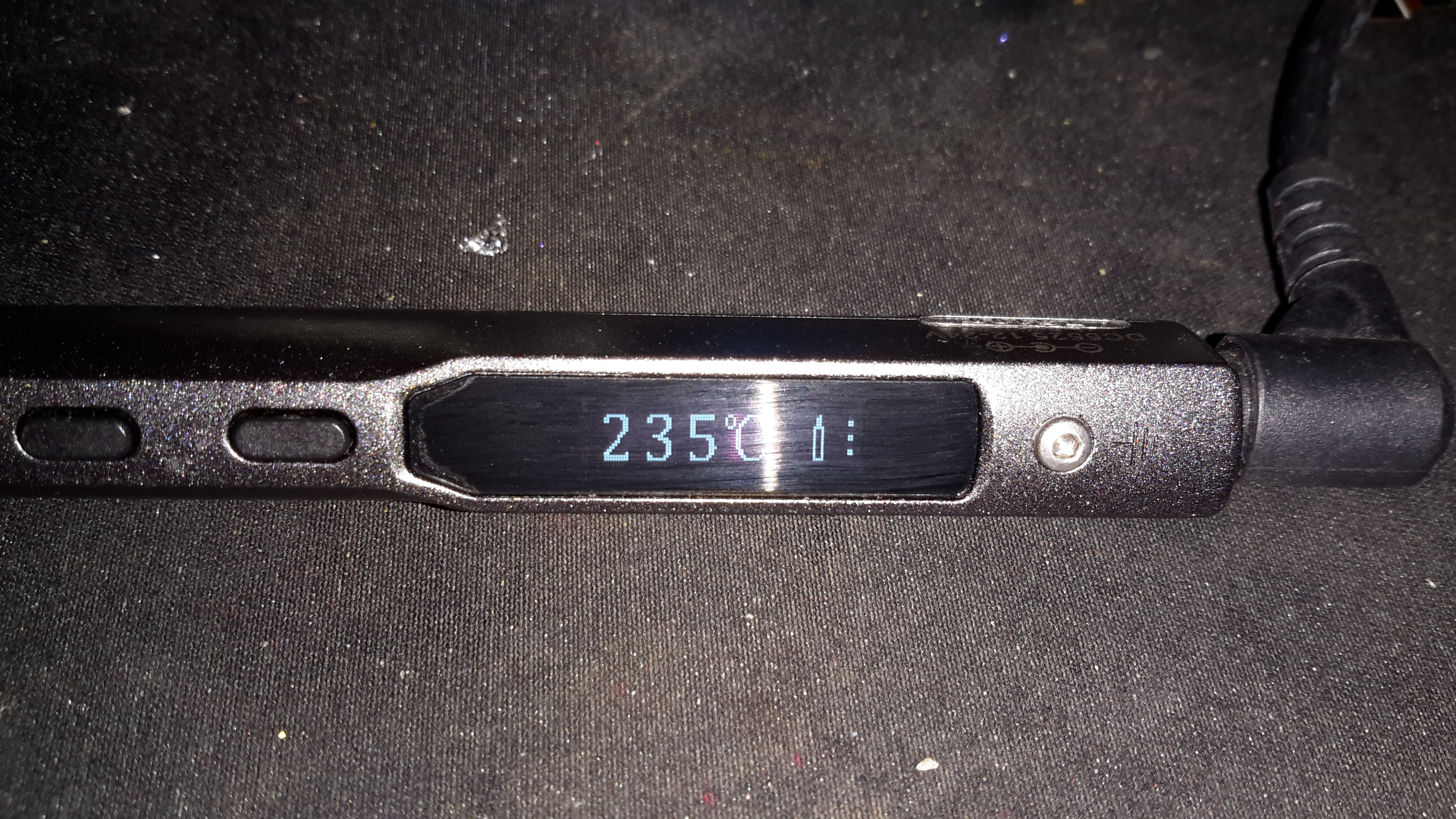
The left hand button starts the heater, which on a 24v input voltage gets to operating temperature well within 10 seconds.
Temperature Stable
The right hand screen icon changes when the temperature has stabilized. The control PCB has an integrated accelerometer, leaving the iron hot for a few minutes triggers a timeout & it powers down. Once picked up again, the heater instantly restarts.
The operating temperature is adjustable with the pair of buttons, from 100°C to 400°C.
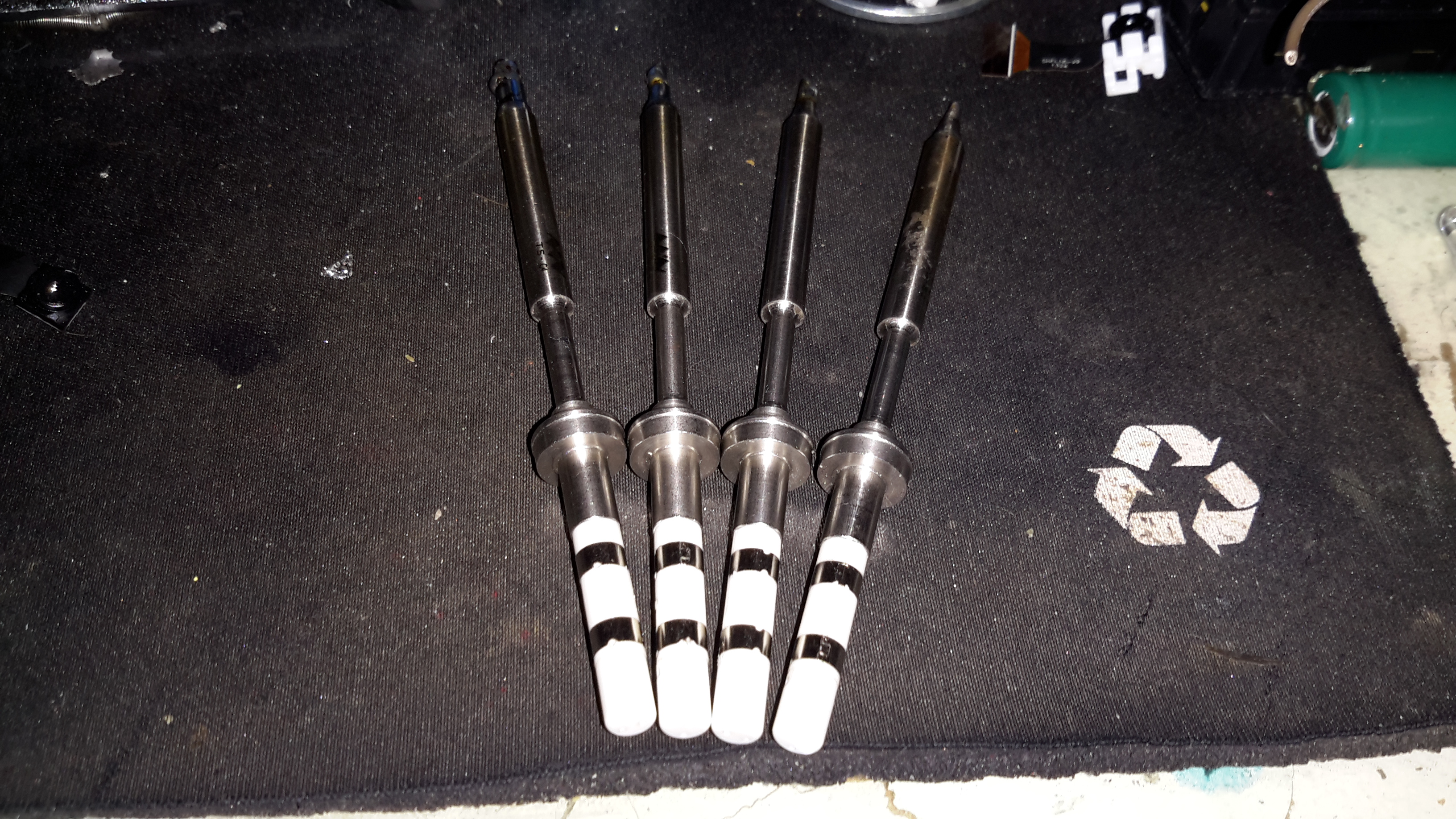
Different Bits
Here’s a selection of bits for the iron. The design is very similar to the Hakko T15 series of irons, but these are a much shorter version. Like the Hakko versions, the actual tips aren’t replaceable, once the bit burns out, the entire assembly is replaced.
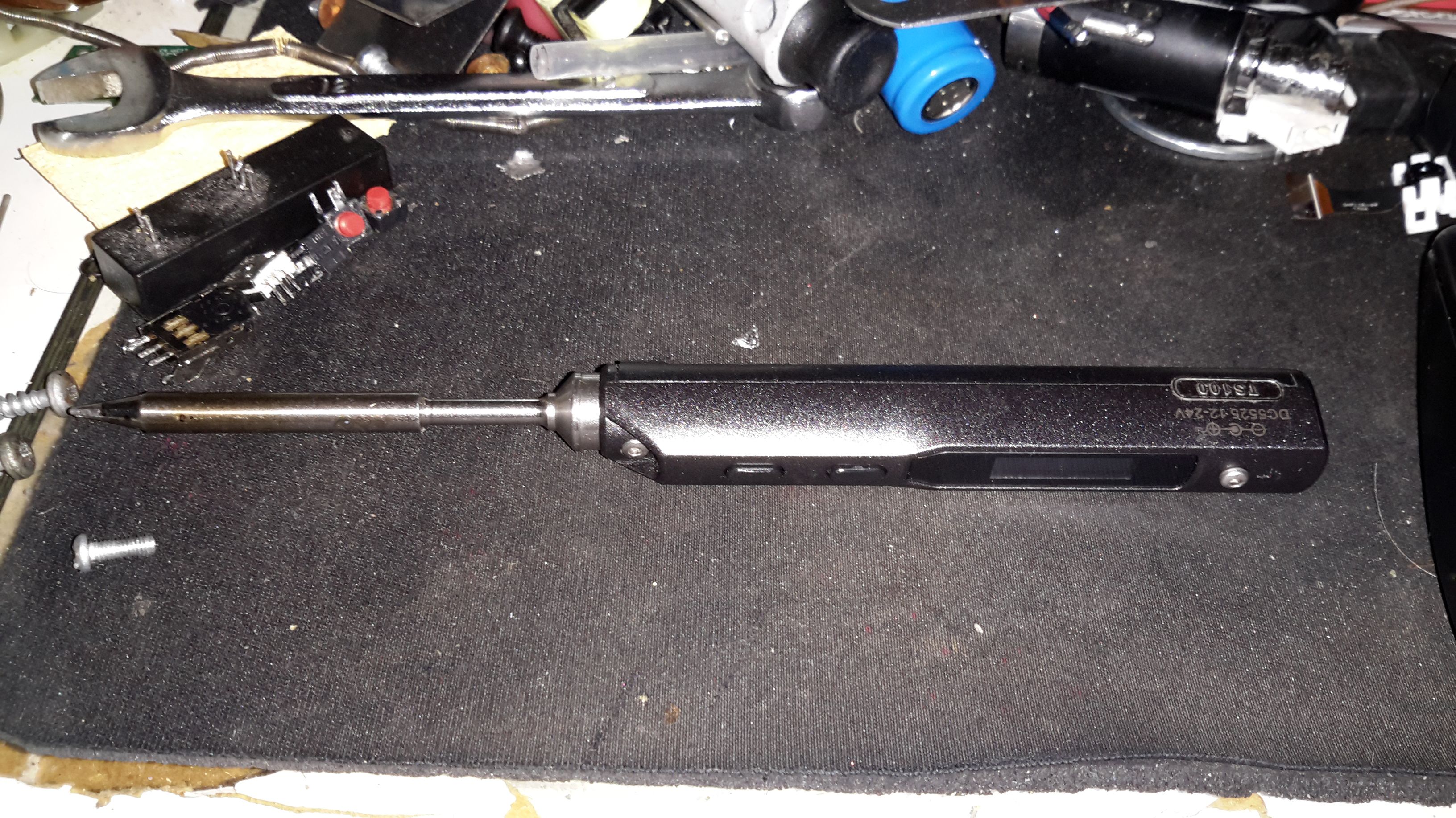
TS100 Soldering Iron
Here’s the iron fully assembled. The entire device is about the same length as just the heating element from a Hakko T15!
Here’s a novel little gadget, a USB powered soldering iron. The heating tip on these is very small & might be useful for very small SMD work. Bigger joints not so much, as it’s only rated at 8W. (Still breaks the USB standard of 2.5W from a single port).
These irons aren’t actually too bad to use, as long as the limitations in power are respected. Since nearly everything has a USB power port these days, it could make for a handy emergency soldering iron.
Heater Socket
The heater & soldering bit are a single unit, not designed to be replaced separately. (I’ve not managed to find replacement elements, but at £3 for the entire iron, it would be pretty pointless).
Above is the socket where the heater plugs in, safely isolating the plastic body from any stray heat.
DC Input Jack
The DC input is a 3.5mm audio jack, a non-standard USB to 3.5mm jack cable is supplied. Such non-standard cables have the potential to damage equipment that isn’t expecting to see 5v on an audio input if it’s used incorrectly.
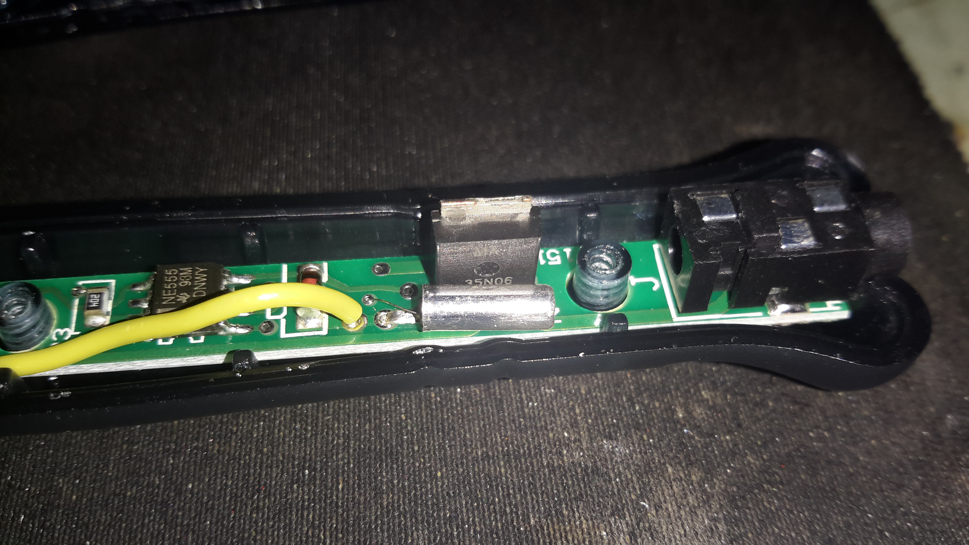
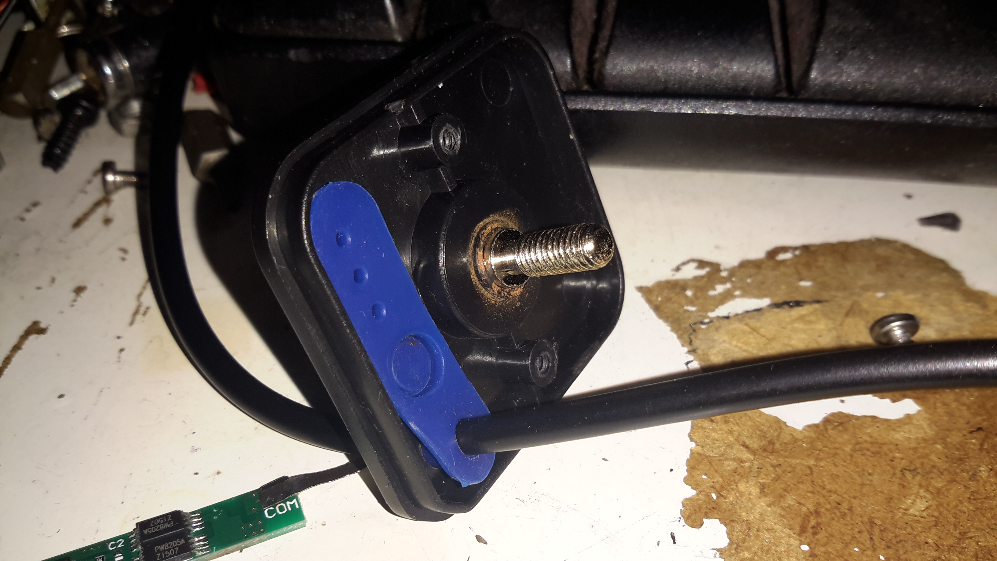
Touch Sensor & LED
There isn’t actually a switch on this unit for power management, but a clever arrangement of a touch button & vibration switch. The vertical spring in the photo above makes contact with a steel ball bearing pressed into the plastic housing, forming the touch contact.
MOSFET
The large MOSFET here is switching the main heater current, the silver cylinder in front is the vibration switch, connected in parallel with the touch button.
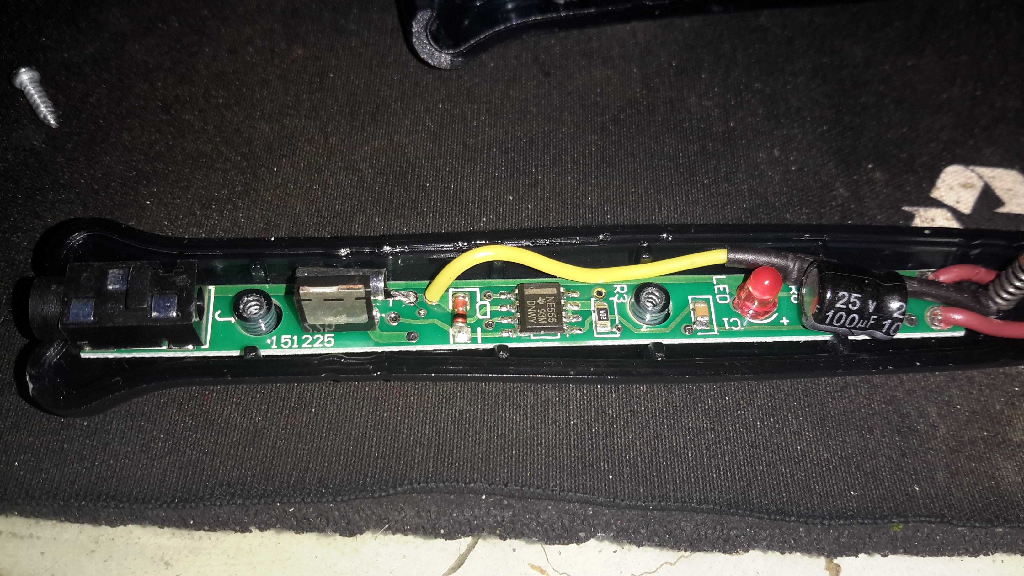
PCB
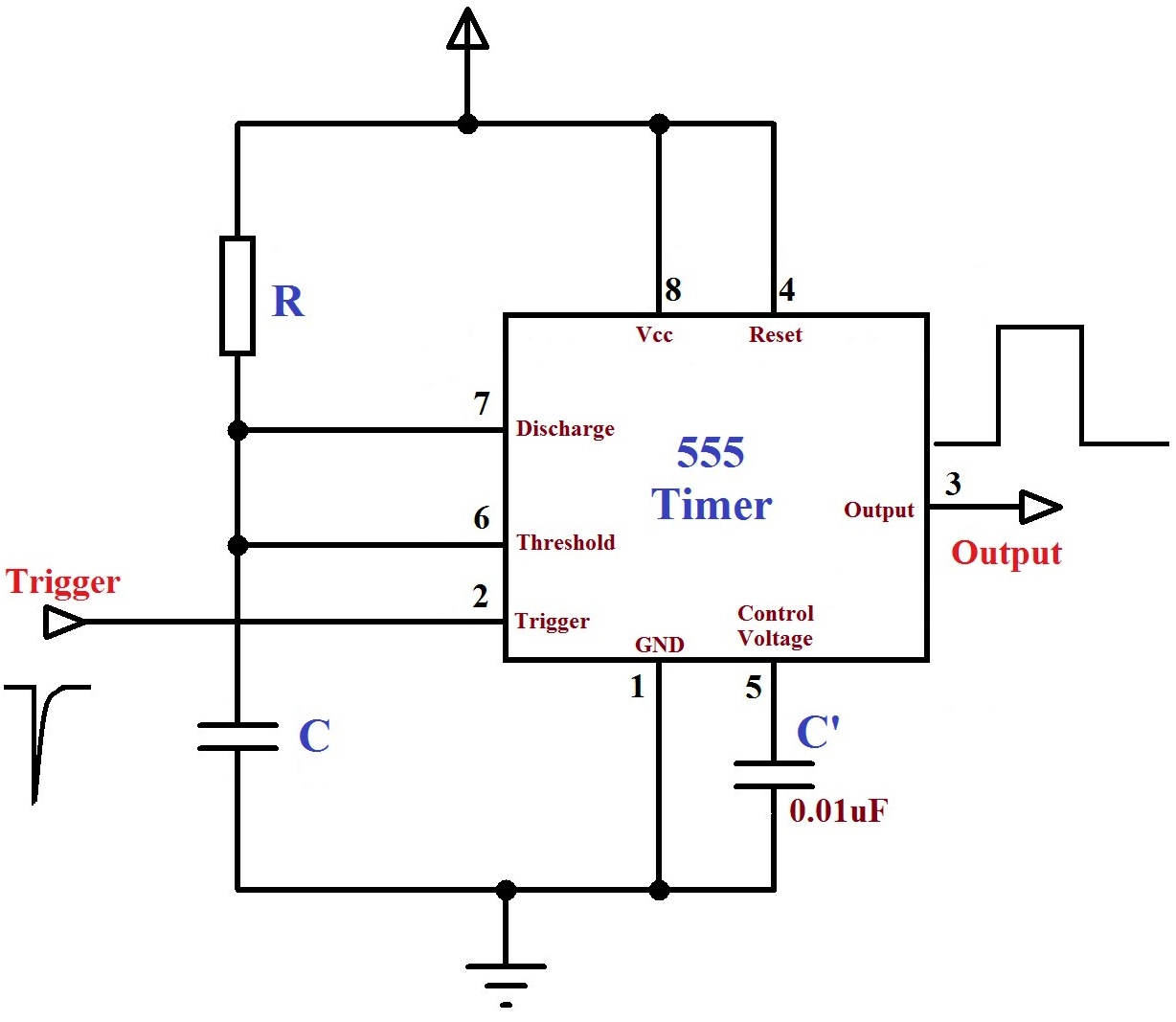
The main controller is very simple. It’s a 555 timer configured in monostable mode. Below is a schematic showing the basic circuit.
555 Monostable
Big Clive also did a teardown & review of this iron. Head over to YouTube to watch.
This website, in various forms, has been around now for about 10 years. Over that time the scope of what I’ve been doing has definitely widened in a big manner.
Considering this, I no longer feel the current website name of “Inside Electronics” is very appropriate, so over the next few weeks, I’ll be re-jigging everything with a new domain name & title:
Experimental Engineering.
The site name is already changed, moving my entire WordPress install over to a new domain will be a bit more labour intensive, with all the internal site links & SEO, so this will be introduced slowly.
(It’s amazing how much this site has evolved over the years, hopefully this evolution will continue!)
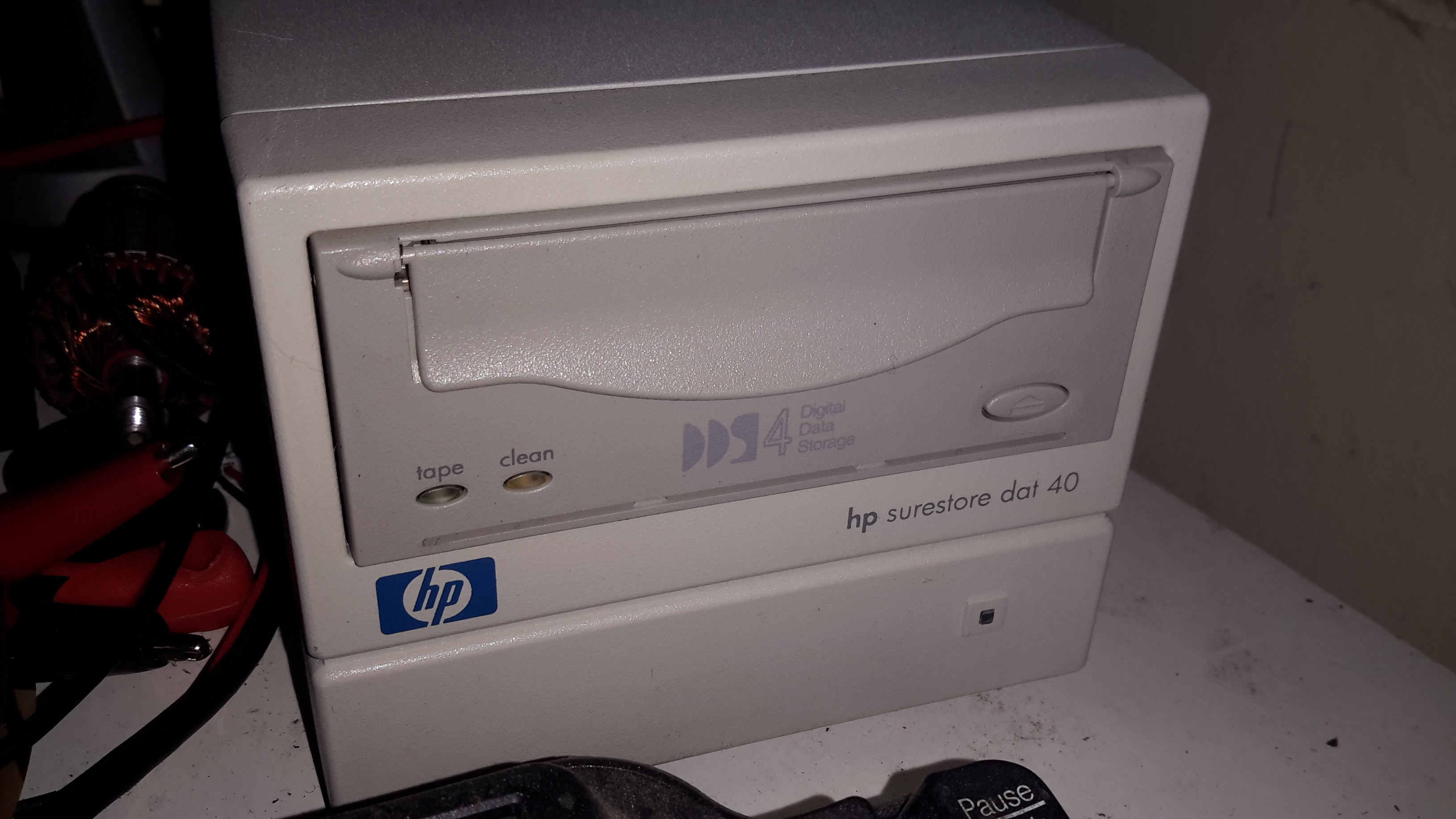
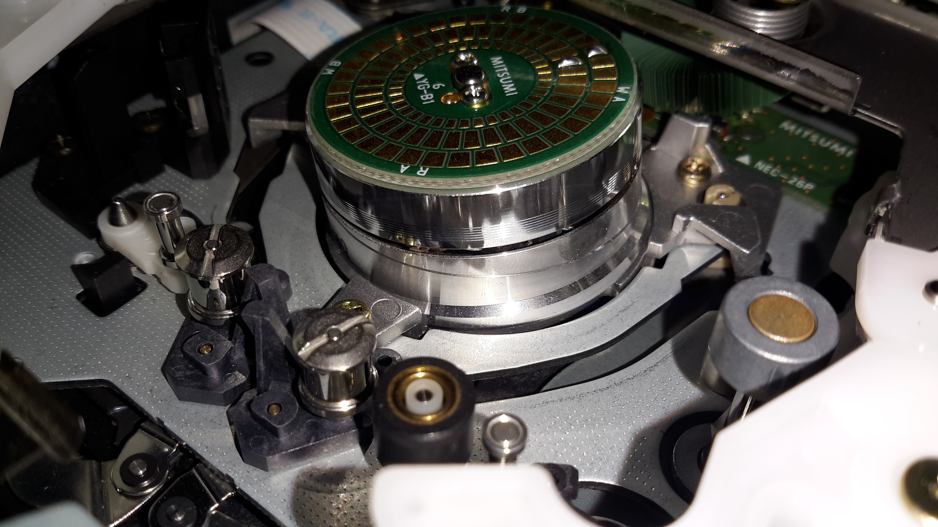
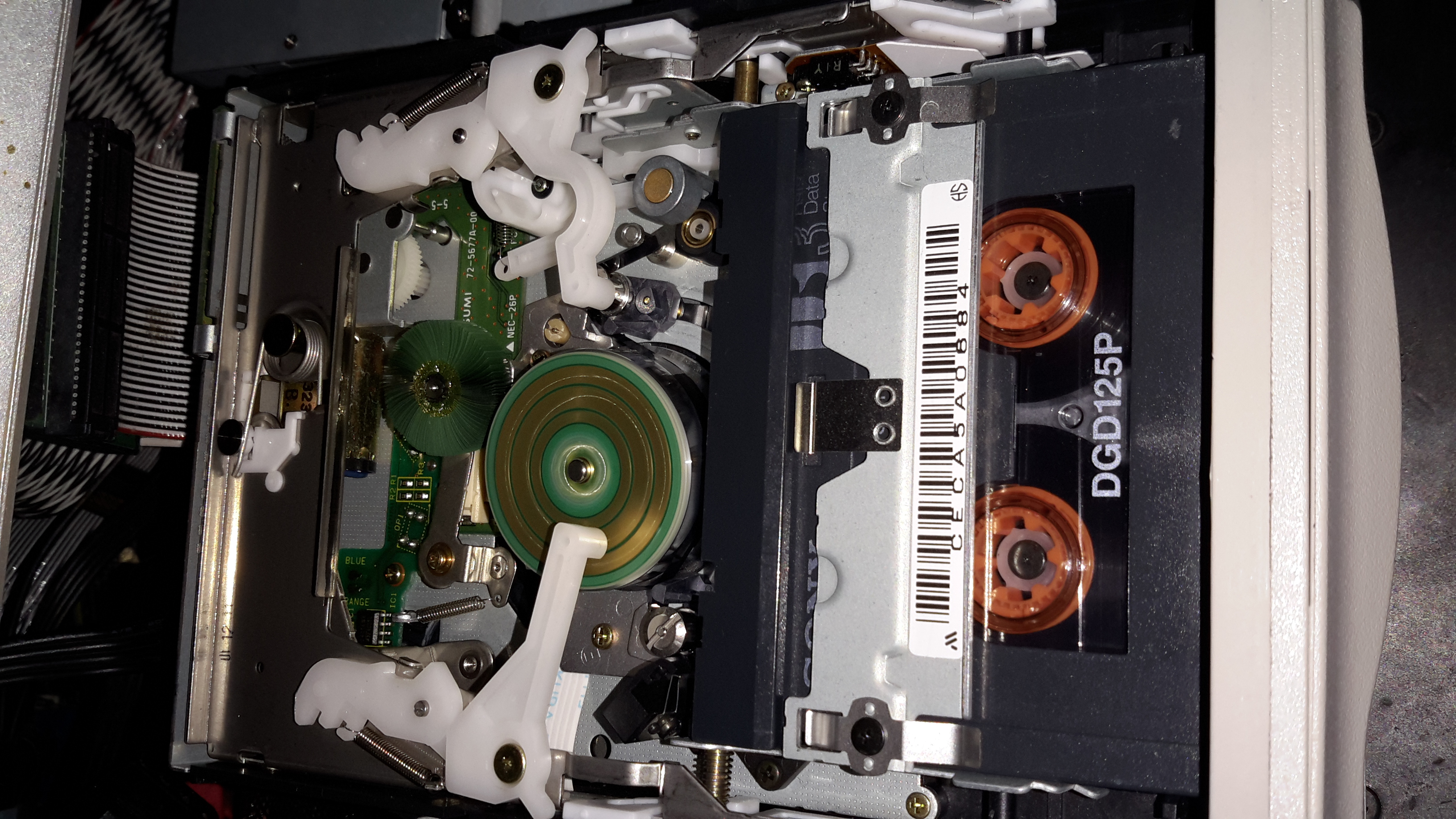
Magnetic tape is the medium of choice for my offline backups & archives, as it’s got an amazing level of durability when in storage. (LTO Has a 30 year archival rating).
For the smaller stuff, like backing up the web server this very site runs on, another format seemed to suit better. Above is a HP DDS4 tape drive, which will store up to 40GB on a cassette compressed.
I picked this format since I already had some tapes, so it made sense.
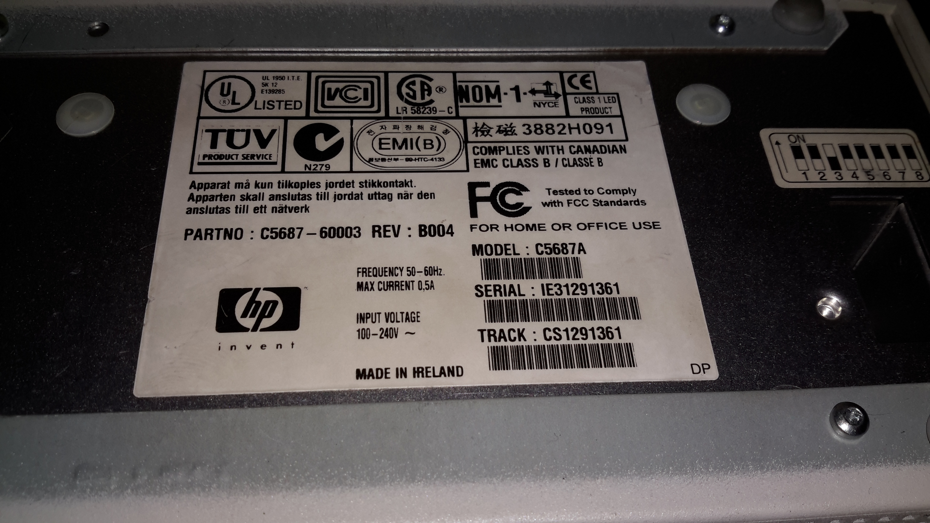
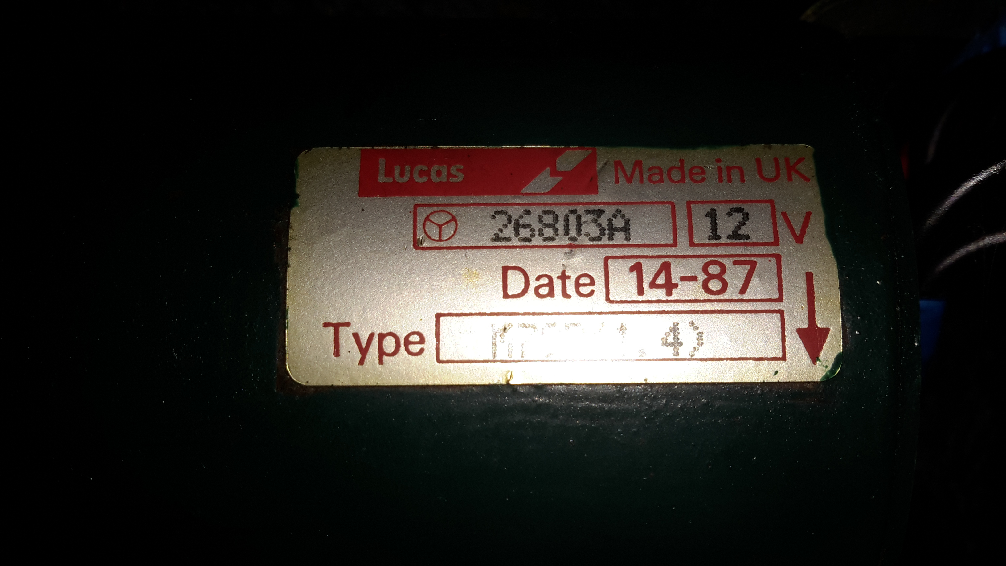
Data Plate
Here’s the info for those who want to know. It’s an older generation drive, mainly since the current generation of tape backup drives are hideously expensive, while the older ones are cheap & plentiful. Unfortunately the older generation of drives are all parallel SCSI, which can be a expensive & awkward to set up. Luckily I already have other parallel SCSI devices, so the support infrastructure for this drive was already in place.
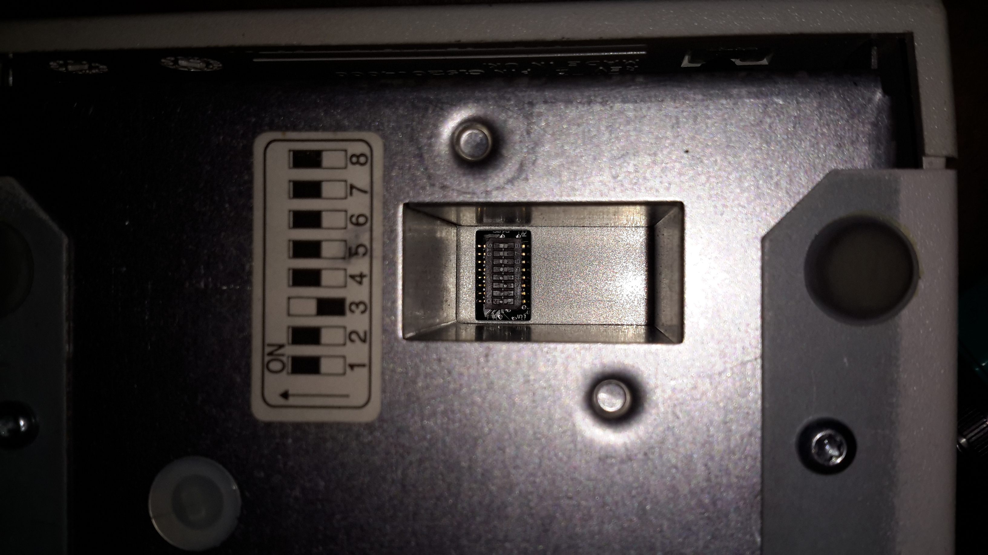
Option Switches
On the bottom of the drive is a bank of DIP switches, according to the manual these are for setting the drive for various flavours of UNIX operating systems. However it doesn’t go into what they actually change.
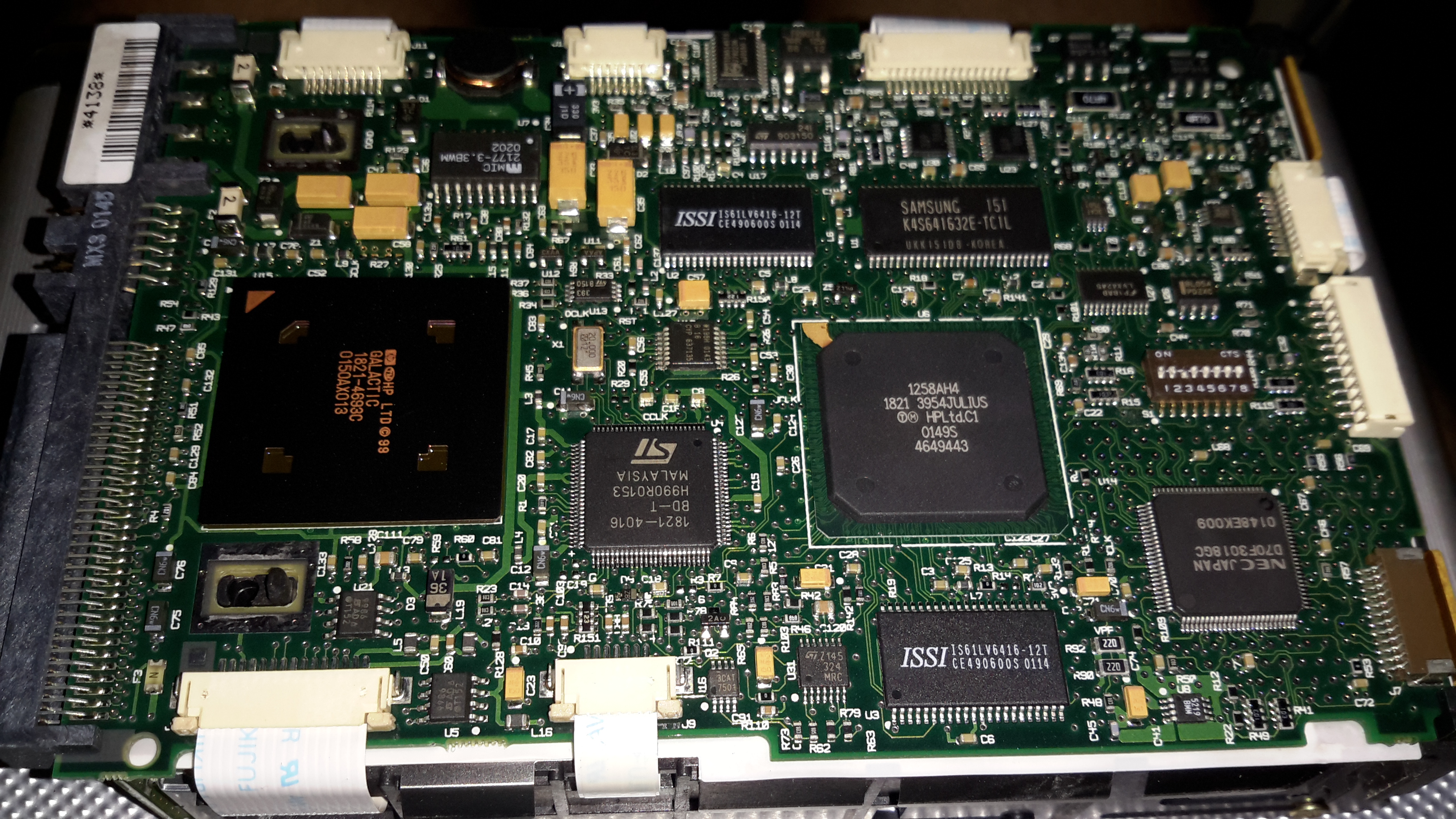
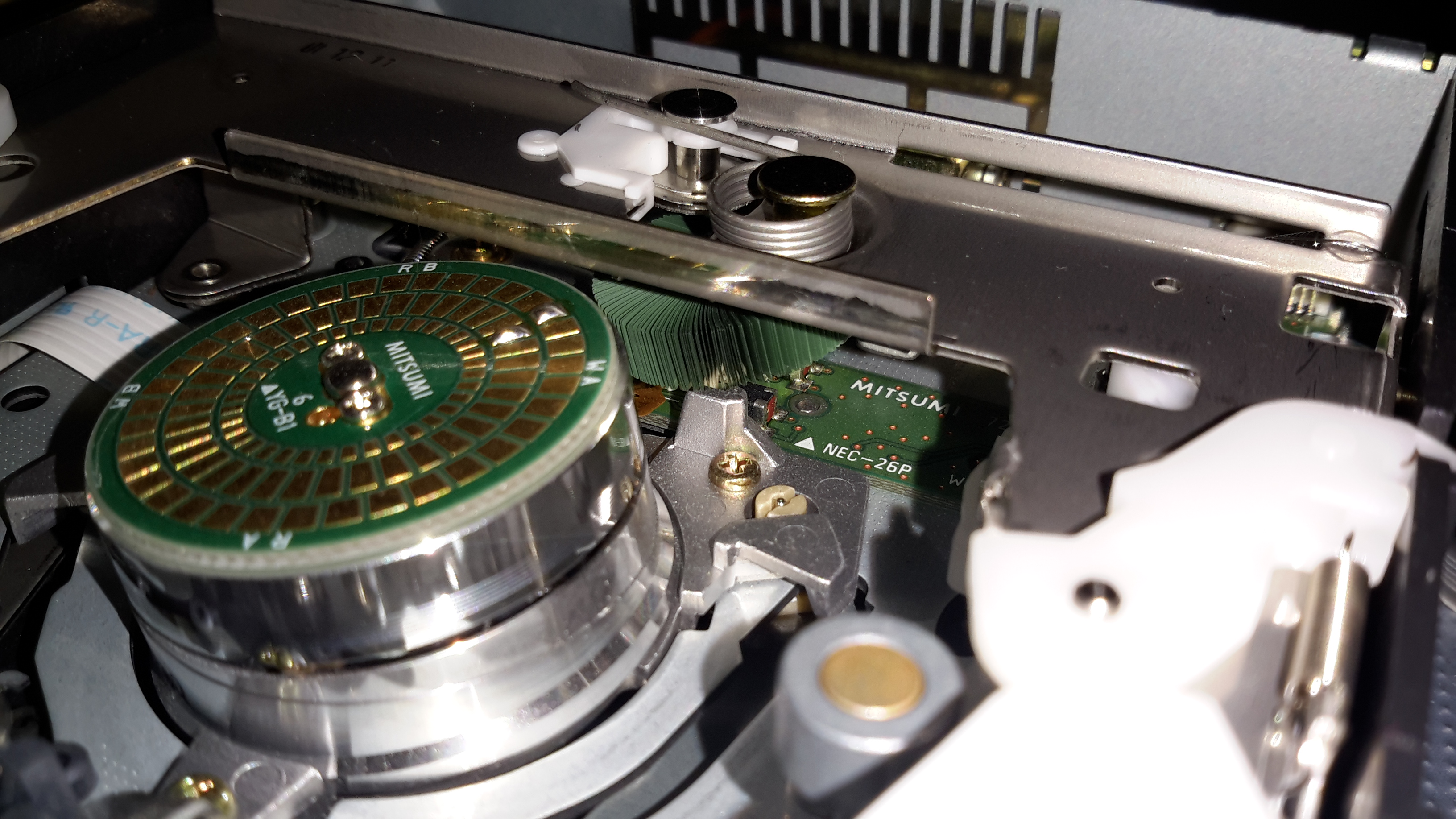
Controller PCB
The bottom of the drive has the control PCB. The large IC on the left is the SCSI interface, I’ve seen this exact same chip on other SCSI tape drives. Centre is a SoC, like so many of these, not much information available.
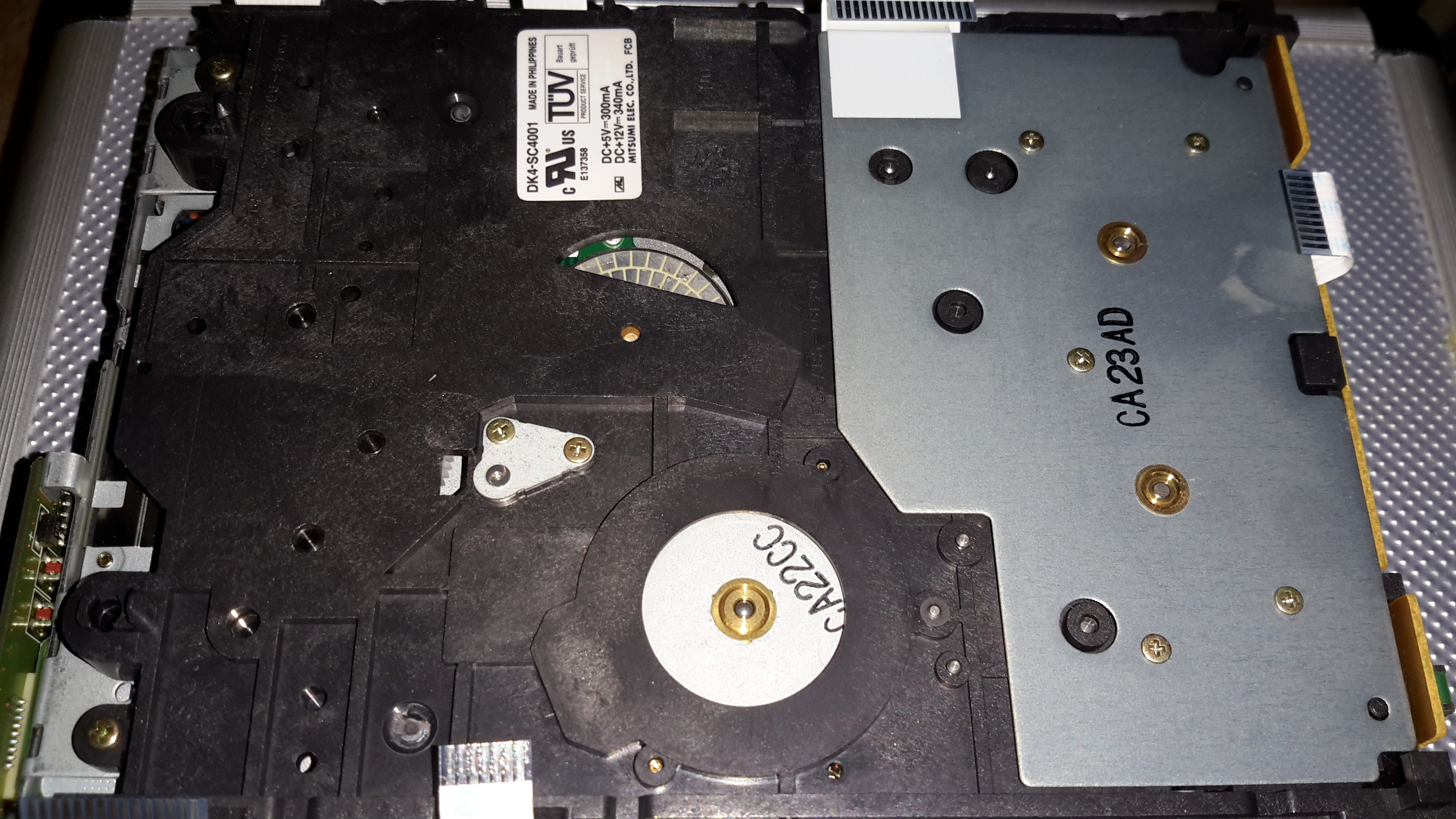
Drive Frame
Removing the board doesn’t reveal much else, just the bottom of the frame with the tape spool motors on the right, capstan motor bottom centre. The bottom of the head drum motor is just peeping through the plastic top centre.
Head Drum
Here’s the head drum itself. These drives use a helical-scan flying head system, like old VHS tape decks. The top of the capstan motor is on the bottom right.
Cleaning Brush
Hidden just under the tape transport frame is the head cleaning brush. I’m not sure exactly what this is made of, but it seems to be plastic.
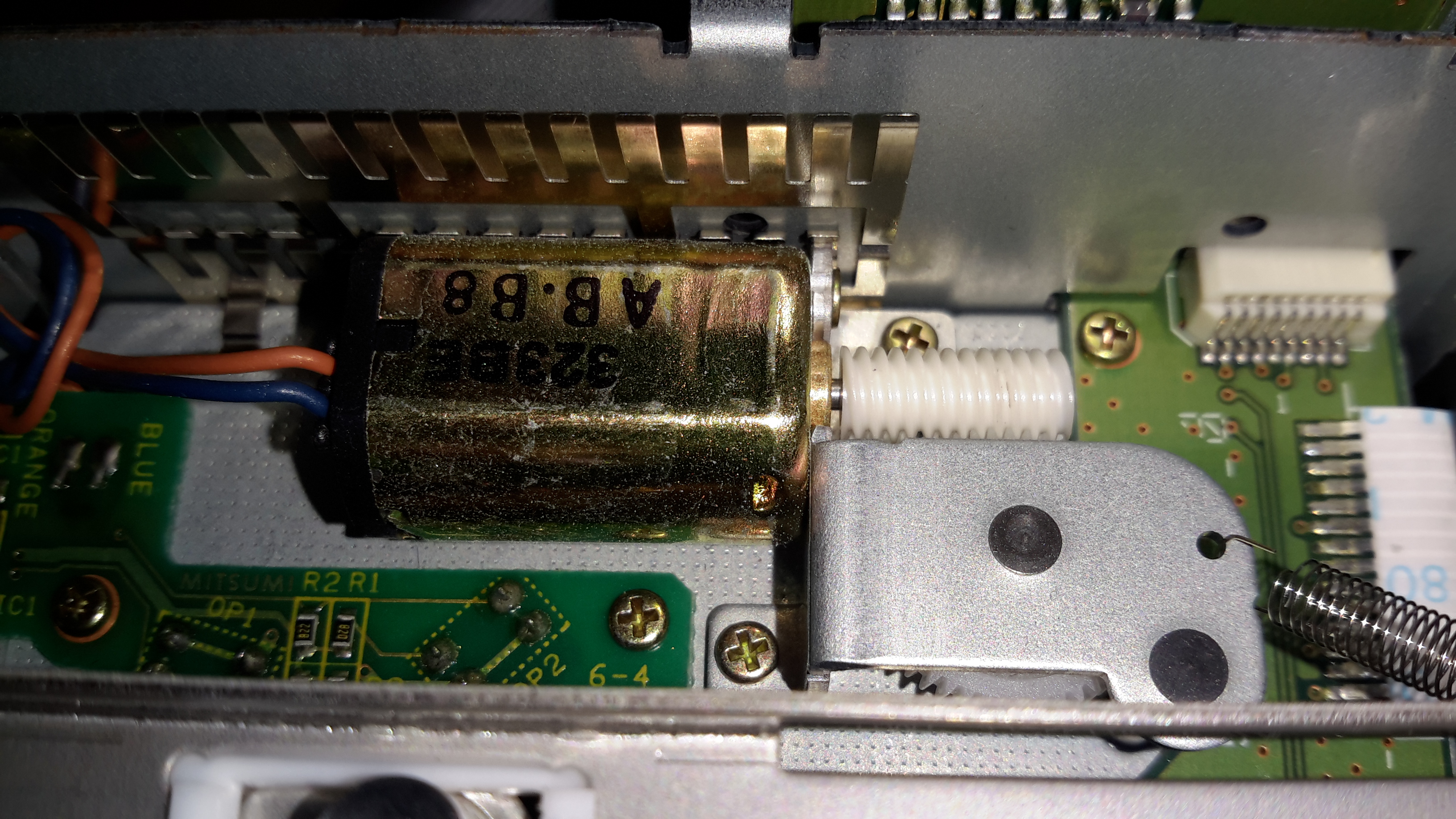
Loading Motor
A single small DC motor with a worm drive handles all tape loading tasks. The PCB to the bottom left of the motor holds several break-beam sensors that tell the drive what position the transport is in.
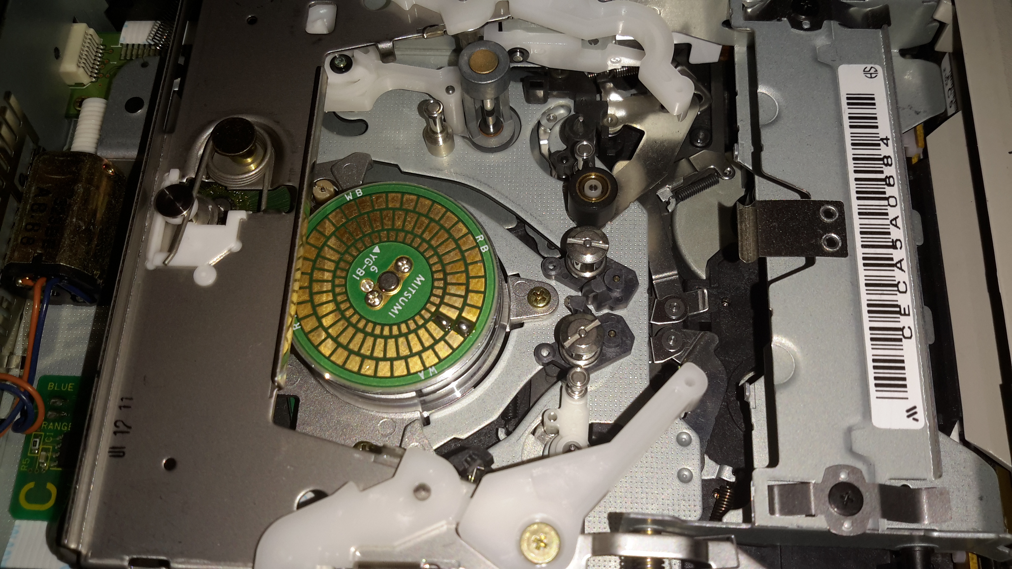
Tape Transport Mech
Here’s the overall tape transport. The PCB on top of the head drum is a novel idea: it’s sole purpose in life is to act as a substrate for solder blobs, used for balancing. As this drum spins at 11,400RPM when a DDS4 tape is in the drive, any slight imbalance would cause destructive vibration.
Tape Transport
Here’s the drive active & writing a tape. (A daily backup of this web server actually). The green head cleaning brush can be better seen here. The drive constantly reads back what it writes to the tape, and if it detects an error, applies this brush momentarily to the drum to clean any shed oxide off the heads. The tape itself is threaded over all the guides, around the drum, then through the capstan & pinch roller.
In the process of going through the boat mechanically, ready for this year’s cruising season, some damage was discovered on the face of the main hydraulic propulsion pump that drives the propeller.
Face Damage
Here’s the front face of the pump, with it’s drive shaft. The circular ridge isn’t supposed to be there, it’s meant to be completely flat.
The central hub of the Centaflex coupling managed to loosen itself on the shaft (they’re pretty badly designed), and when the steel hub moved backward, it ground a very nice recess into the cast iron pump housing.
This managed to get deep enough where it compromised the circlip groove that holds both the oil seal & the mainshaft thrust bearing in place.
Spacer Ring
To save a considerable amount of cash (replacing the entire base casting of the pump would be hideously expensive), a 6mm ring was machined from steel, to hold the seal in place.
The face of the pump was then drilled & tapped for M5 screws.
Plate Fitted
Above, the repair plate has been fitted, with the spacer ring sandwiched between it & the oil seal, securing everything in place.
Having a replaceable wear plate screwed to the front of the pump also allows for easy future repair if the coupling moves again.
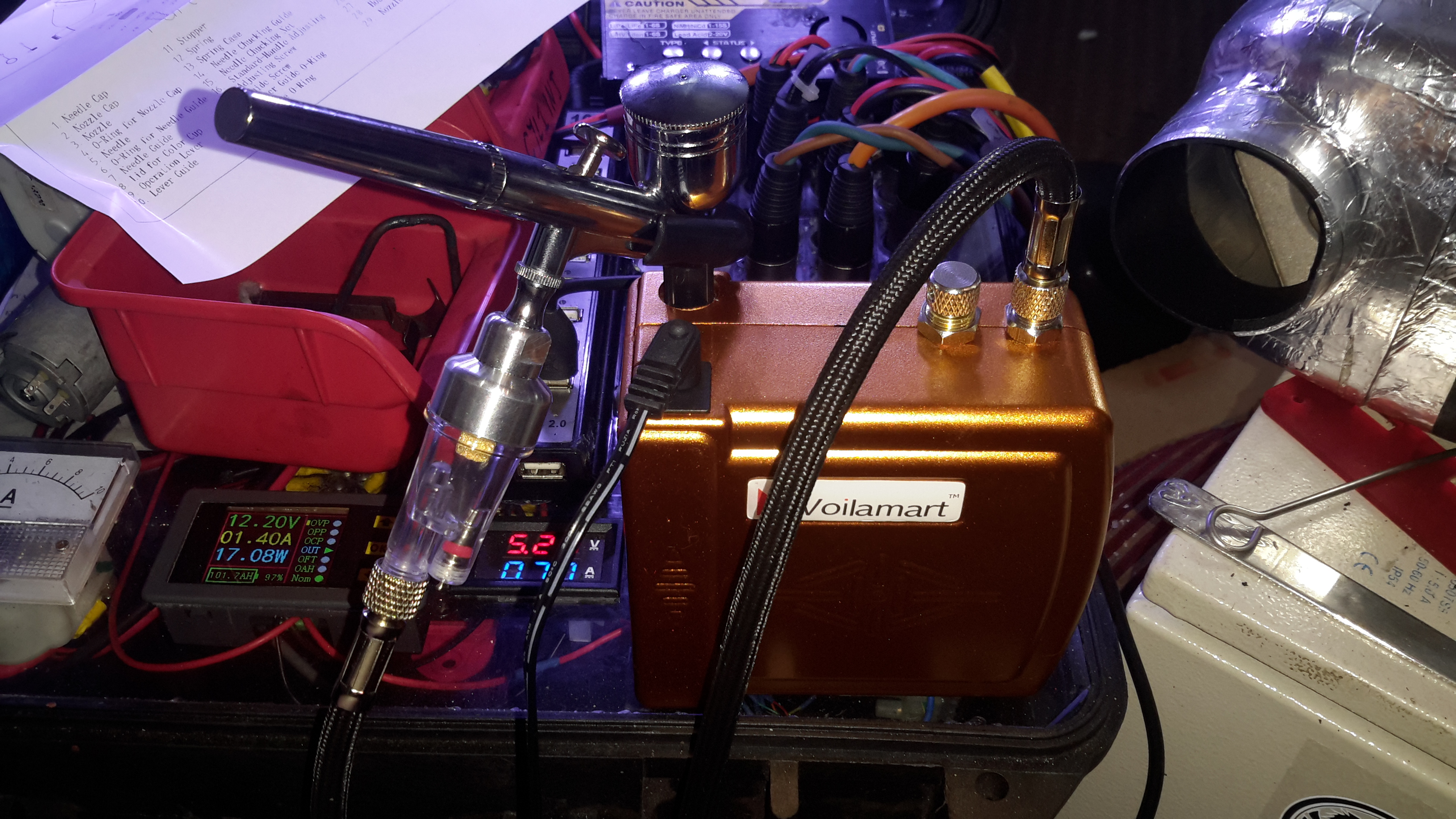
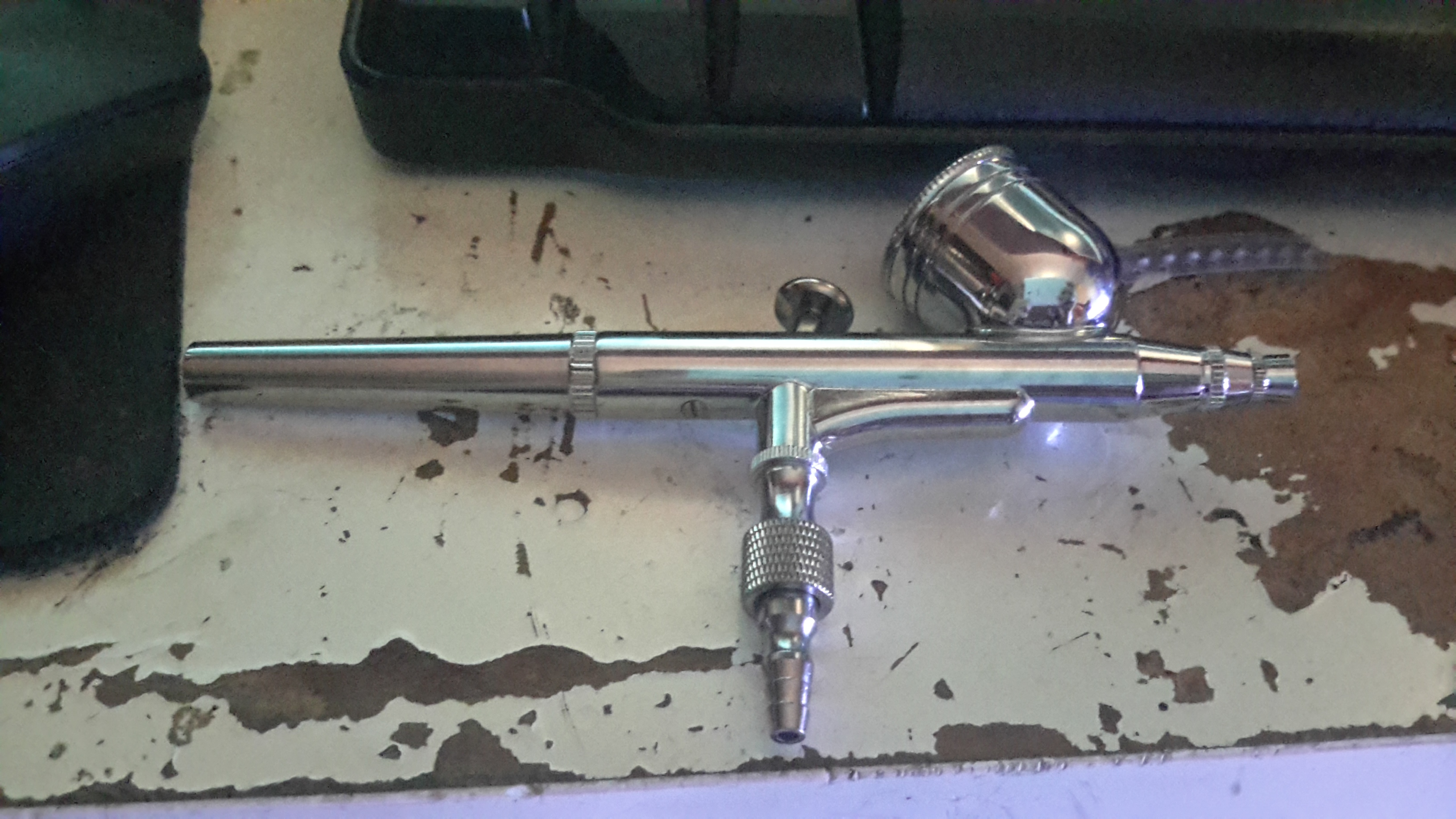
For my latest project, I needed an easier way to paint without messing about with brushes, and the associated marks they leave in a paint job. eBay provided me with a cheap airbrush & compressor.
Airbrush Kit
For less than £30, this kit doens’t look so bad. I’ve never used an airbrush before, but I’ve had no problems with this as yet spraying both water based paints & solvent based paints.
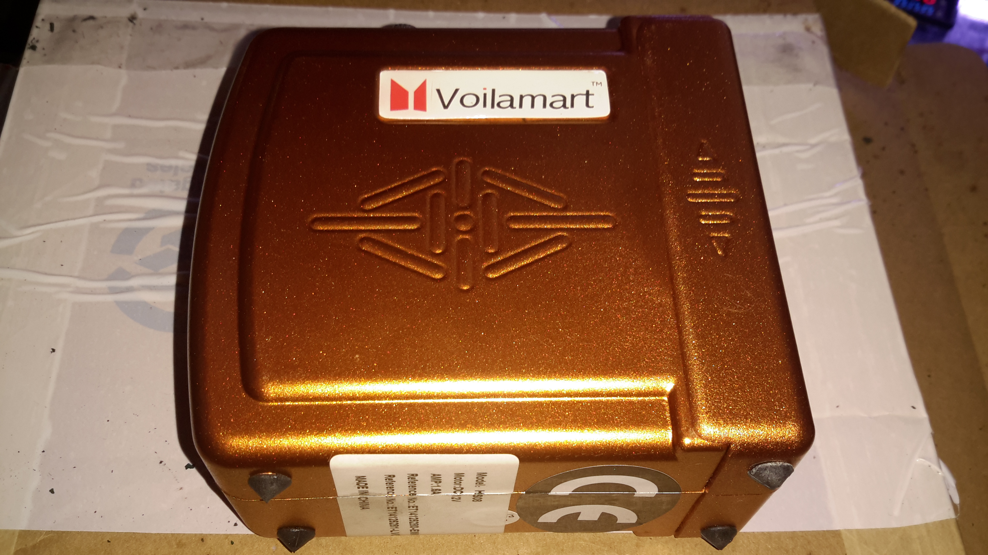
Compressor
Here’s the compressor itself, this runs on 12v & has an output pressure of 1.5 Bar, which is supposed to be adjustable.
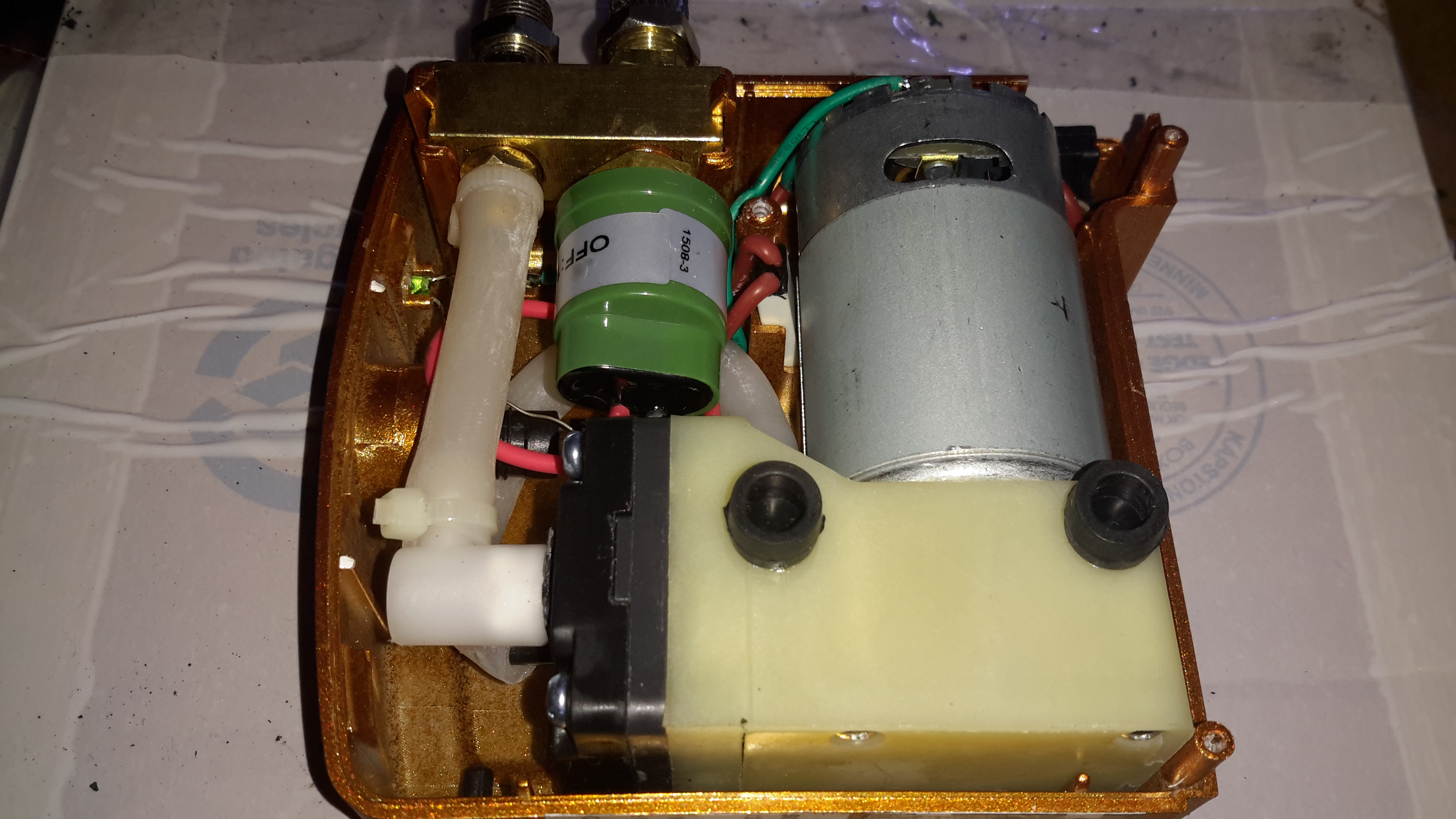
Compressor Internals
Removing a couple of screws reveals the internal components. Nothing much unusual here, a DC diaphragm pump, pressure switch & outlet fittings. There’s also a thermal cutout fitted next to the motor for protection.
The pressure switch attached to the manifold trips at 1.5Bar, keeping the pressure to the brush pretty much constant.
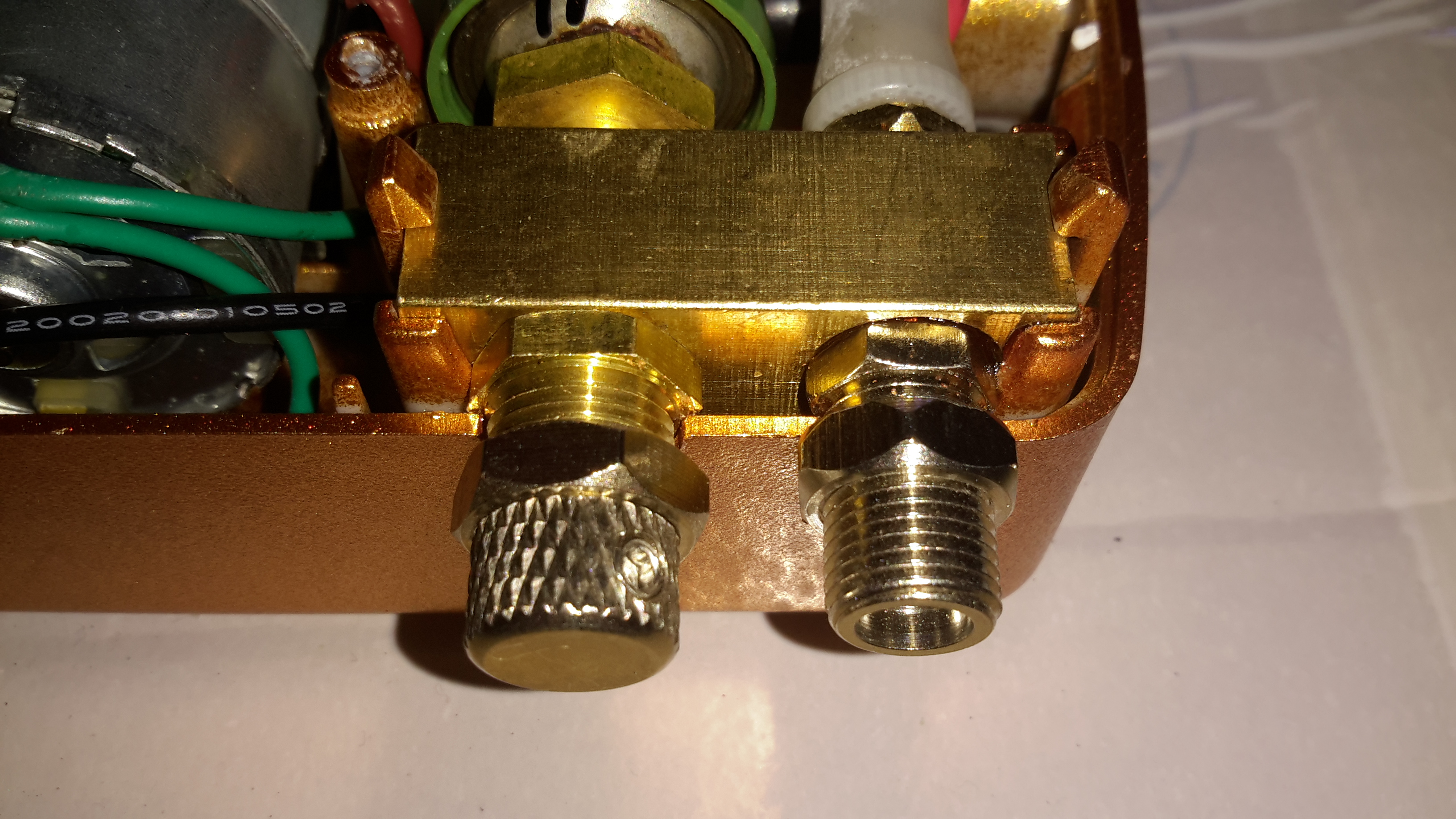
Air Block
Next to the air outlet fitting is an adjustment knob, supposedly for varying the pressure. However it’s just a piss-poorly designed adjustable relief valve that vents to atmosphere. There’s not much of a control range.
Messy Wiring
The wiring gets a bit messy where the power LED is concerned, with no heatshrink over the solder joints, but it’s adequate.
Airbrush
The airbrush itself isn’t too bad. It’s solid Brass, with a very nice Chrome finish. I’m not expecting miracles from a very cheap tool, but it certainly seems to be reasonable.
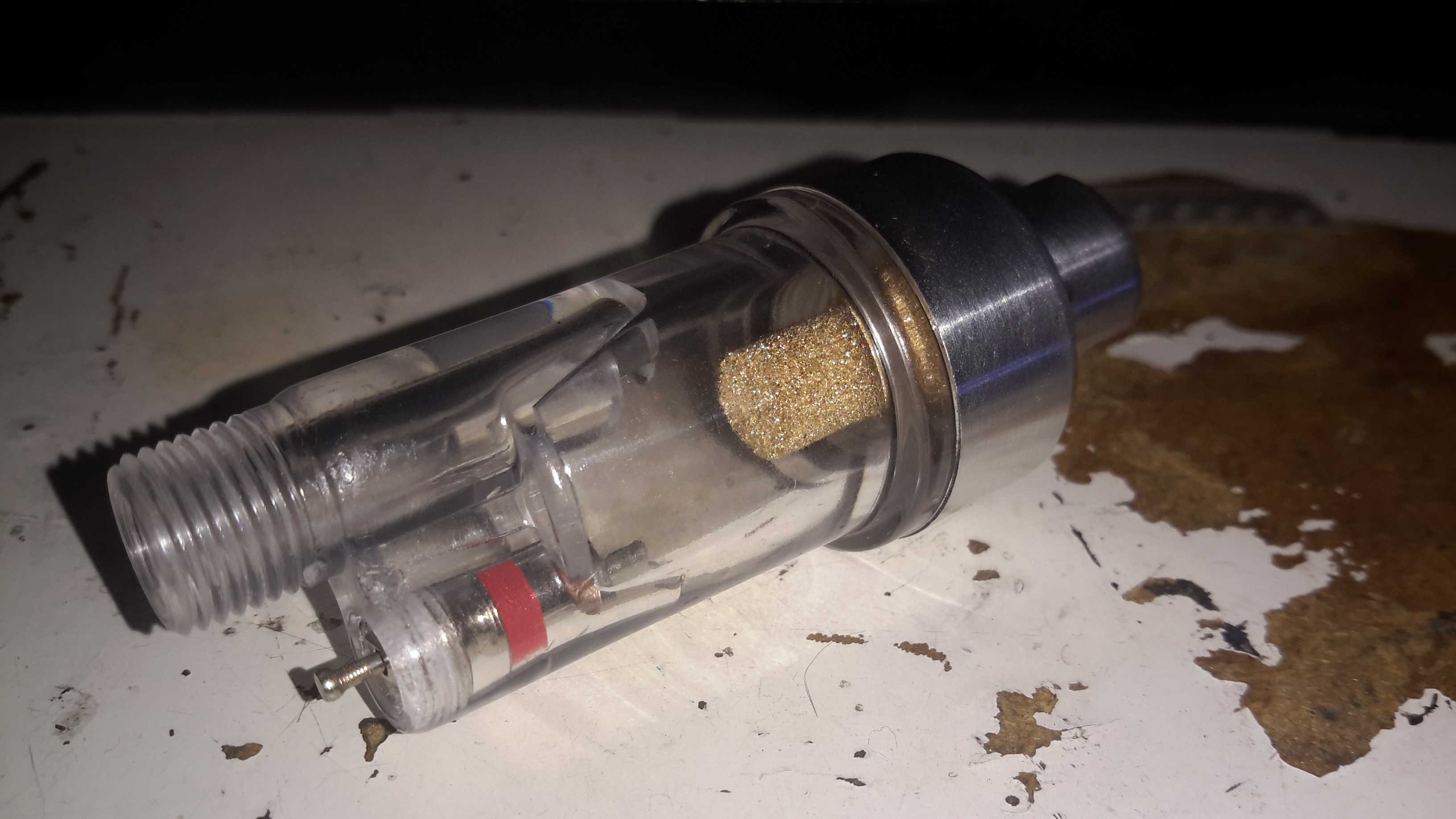
Water Trap
A moisture trap is supplied for the brush, to prevent water drops being sprayed out with the paint. Very handy.
Just a quick note for the regular (and not so regular) readers:
My server infrastructure is currently going through some migration & upgrade processes, so for the next few days the site might be a little on the slow side, but hopefully I can get everything sorted out quickly!
During this time please bear with the slower than normal response times.
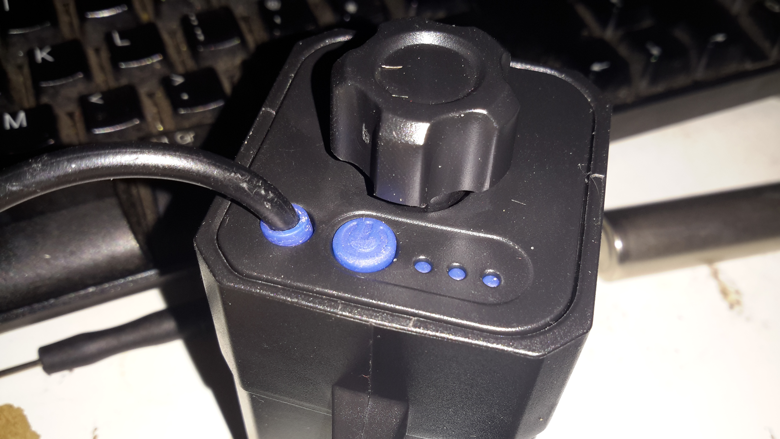
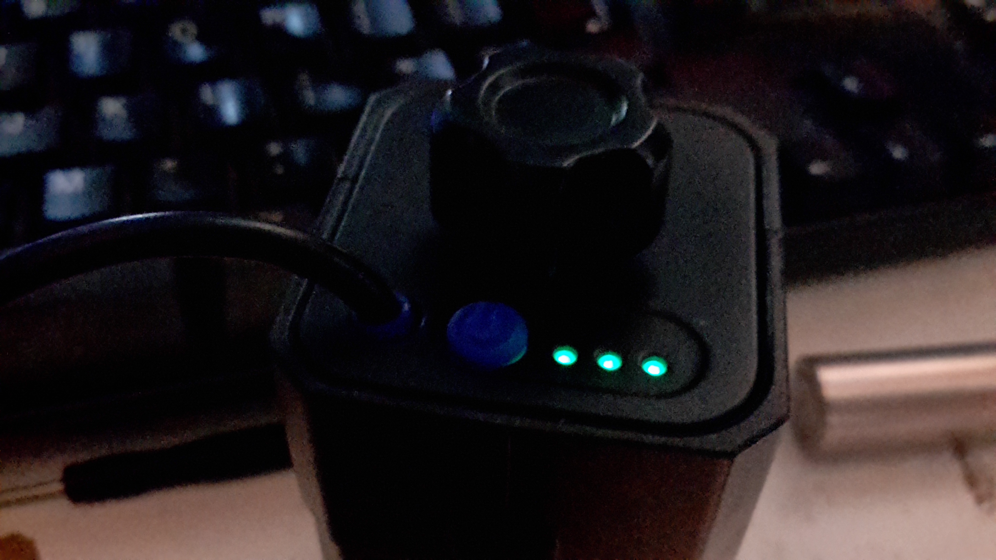
Since the 4×18650 battery pack supplied with my Cree head torch is pretty shit, even by China’s standards, I figured something I could put my own cells into would be a better option. An eBay search turned up these battery boxes, not only with a direct battery output for my torch, but also a USB port for charging other devices when I’m low on charge.
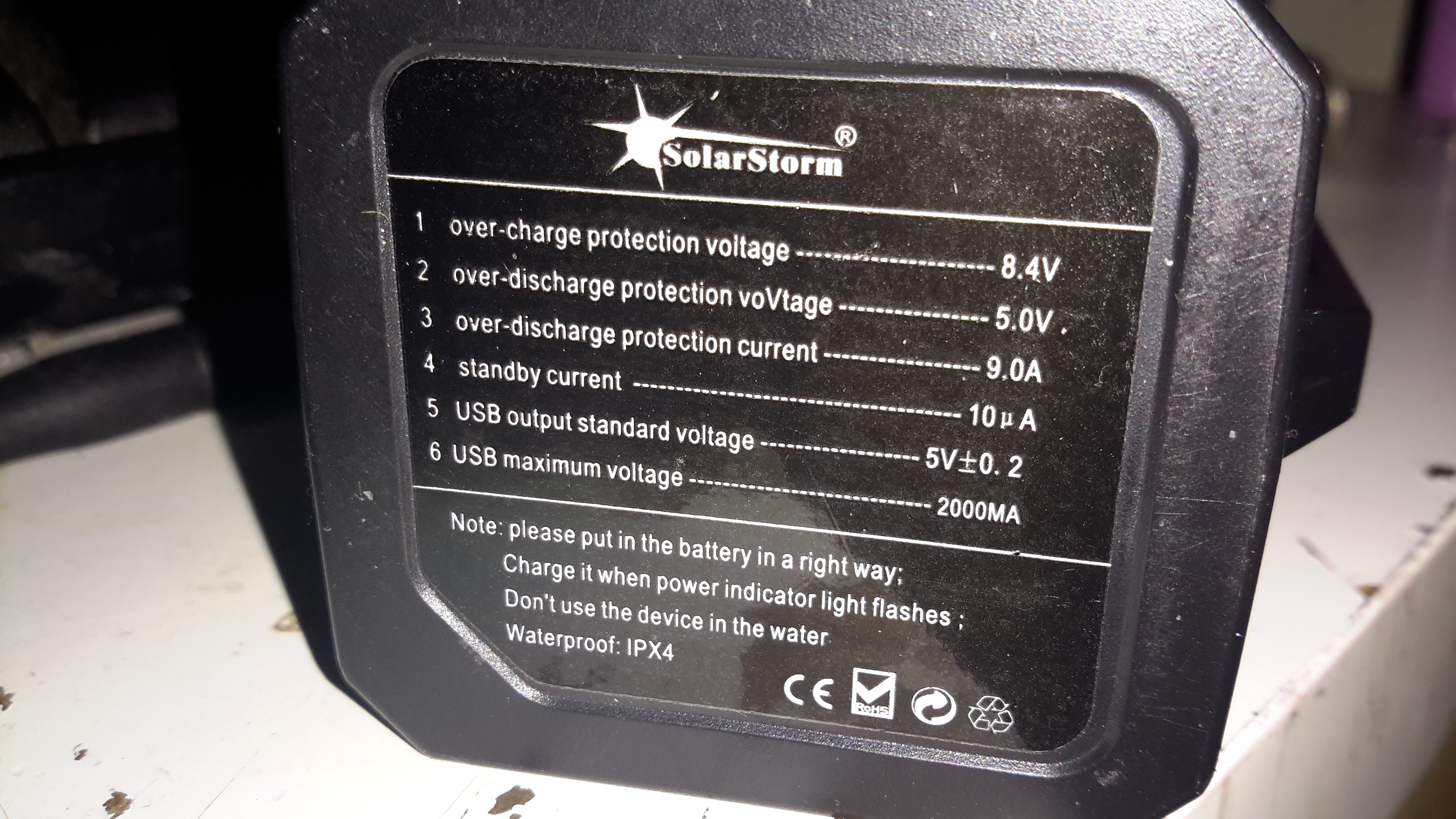
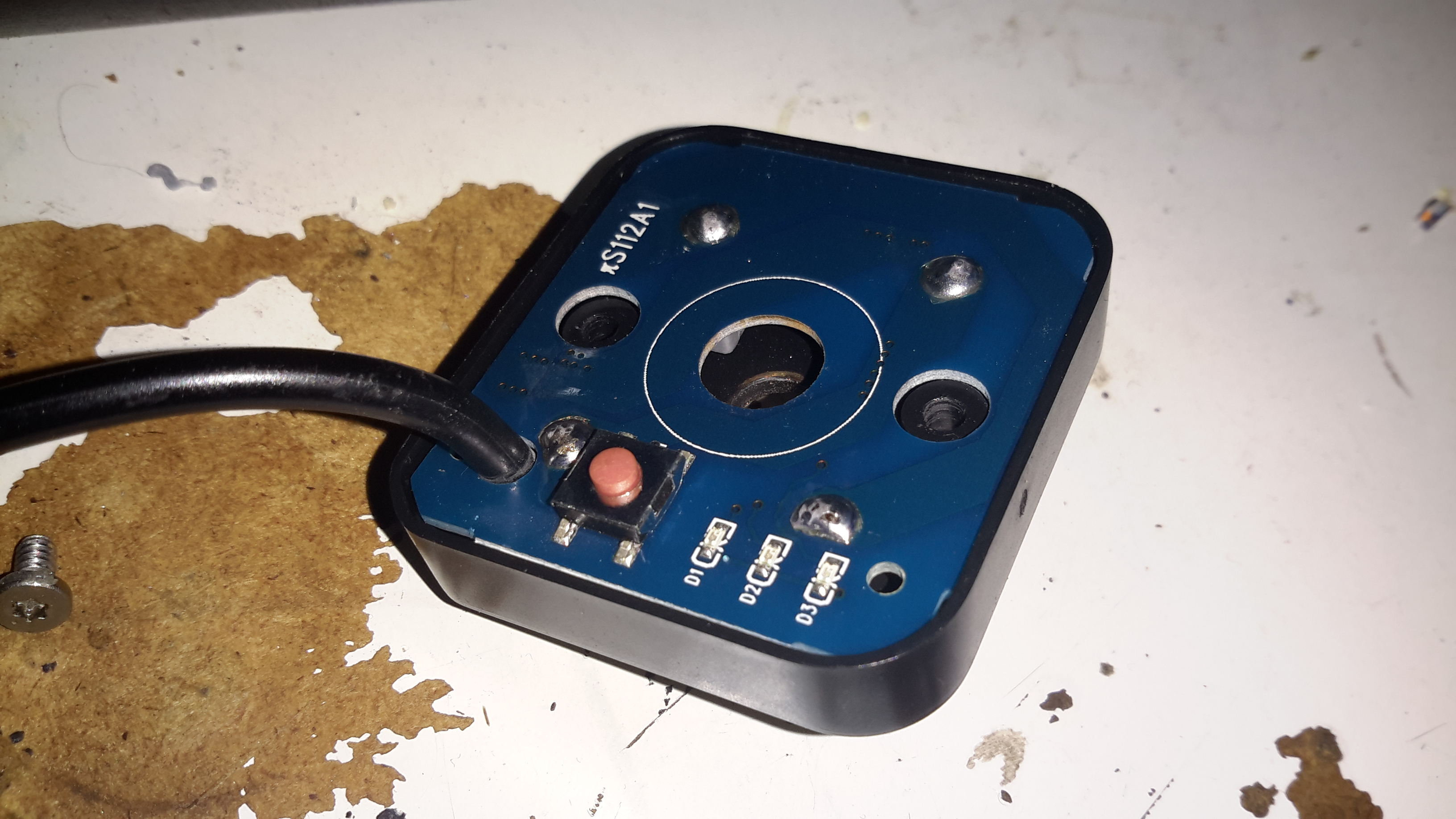
LED Capacity Indicator
The output to the lamp connector is directly connected to the battery, through the usual Lithium Ion protection, but the USB output is controlled from a single power button. Battery charge condition is displayed on 3 LEDs. Not sure why they used blue silicone for the seal & then used green LEDs… But it does work, even if a little dim.
Label
Essential information. Does claim to be protected, and from the already existing electronics for the USB this would be expected in all but the cheapest crap.
An IP rating of IPX4 is claimed, yet just above that rating is a notice not to be used in water. Eh?
This is sealed with an O-Ring around the edge of the top cap & silicone seals around the cable & retaining screw. I did test by immersion in about 6″ of water, and it survived this test perfectly fine, no water ingress at all.
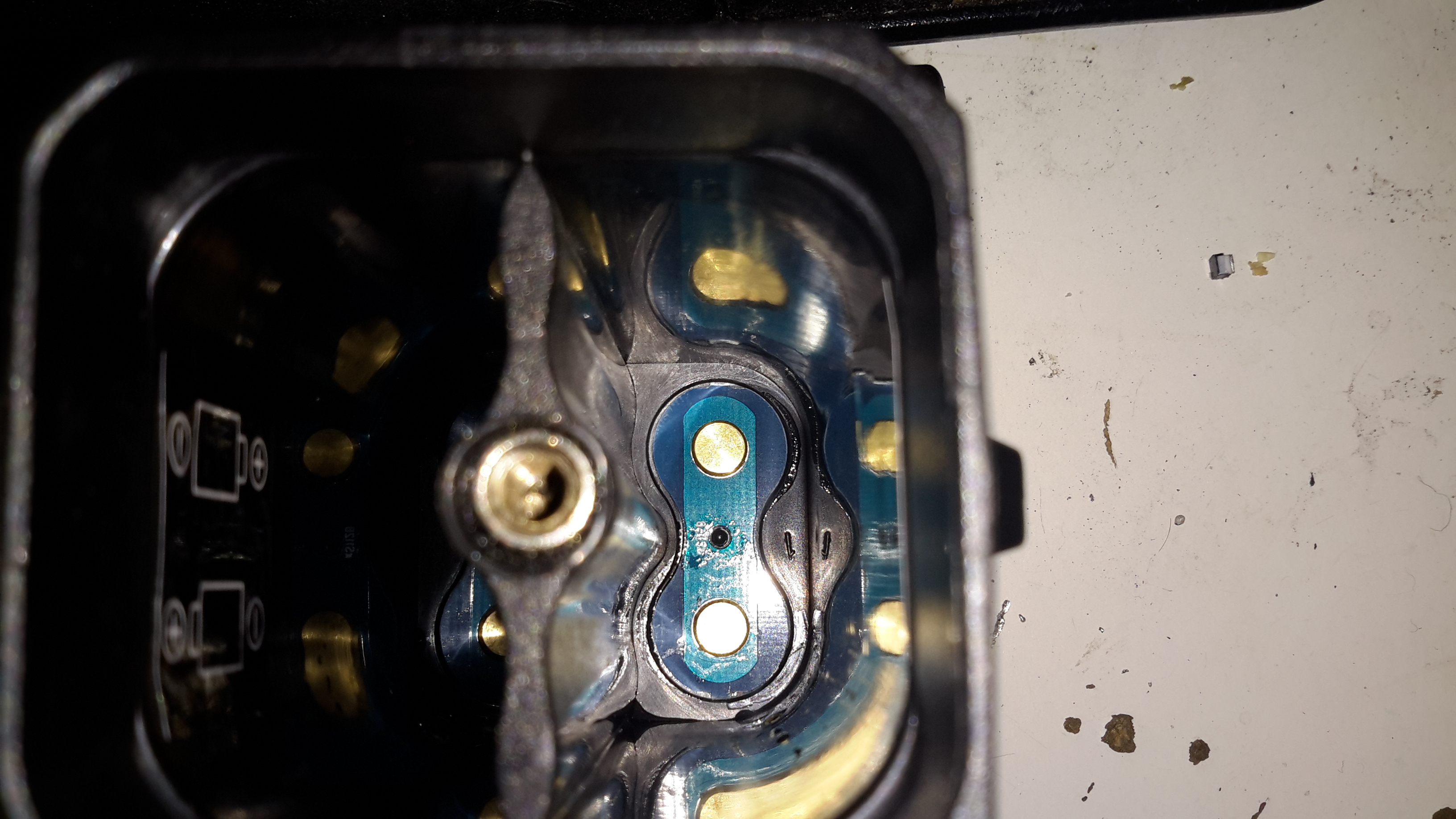
Interconnect Straps
The casing holds a PCB at the bottom end with the cell straps.
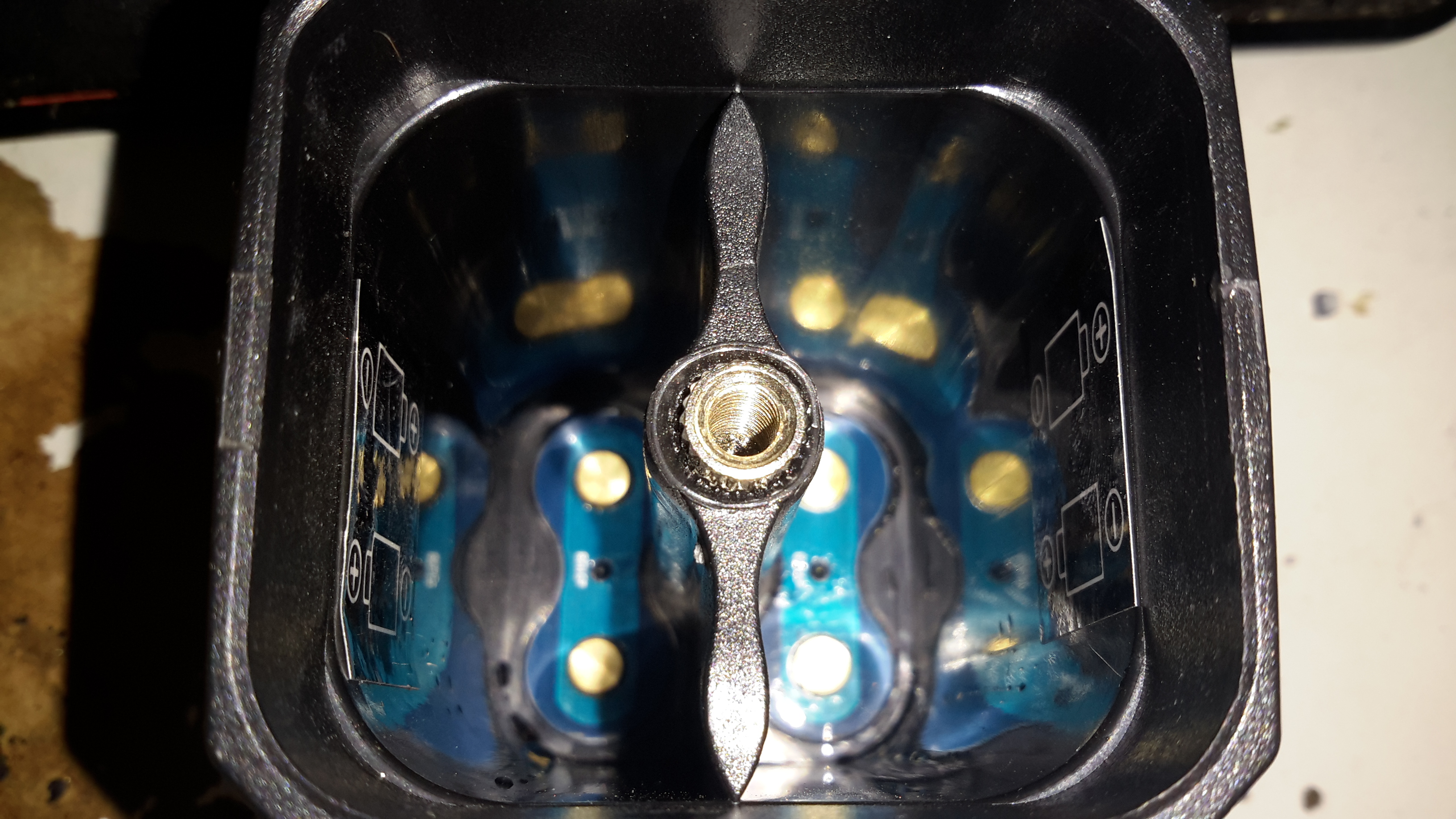
Screw Post
Someone wasn’t that careful at getting the brass screw insert properly centred in the injection mould when they did this one. It’s mushed off centre, but i’s solidly embedded & doesn’t present any problems to usability.
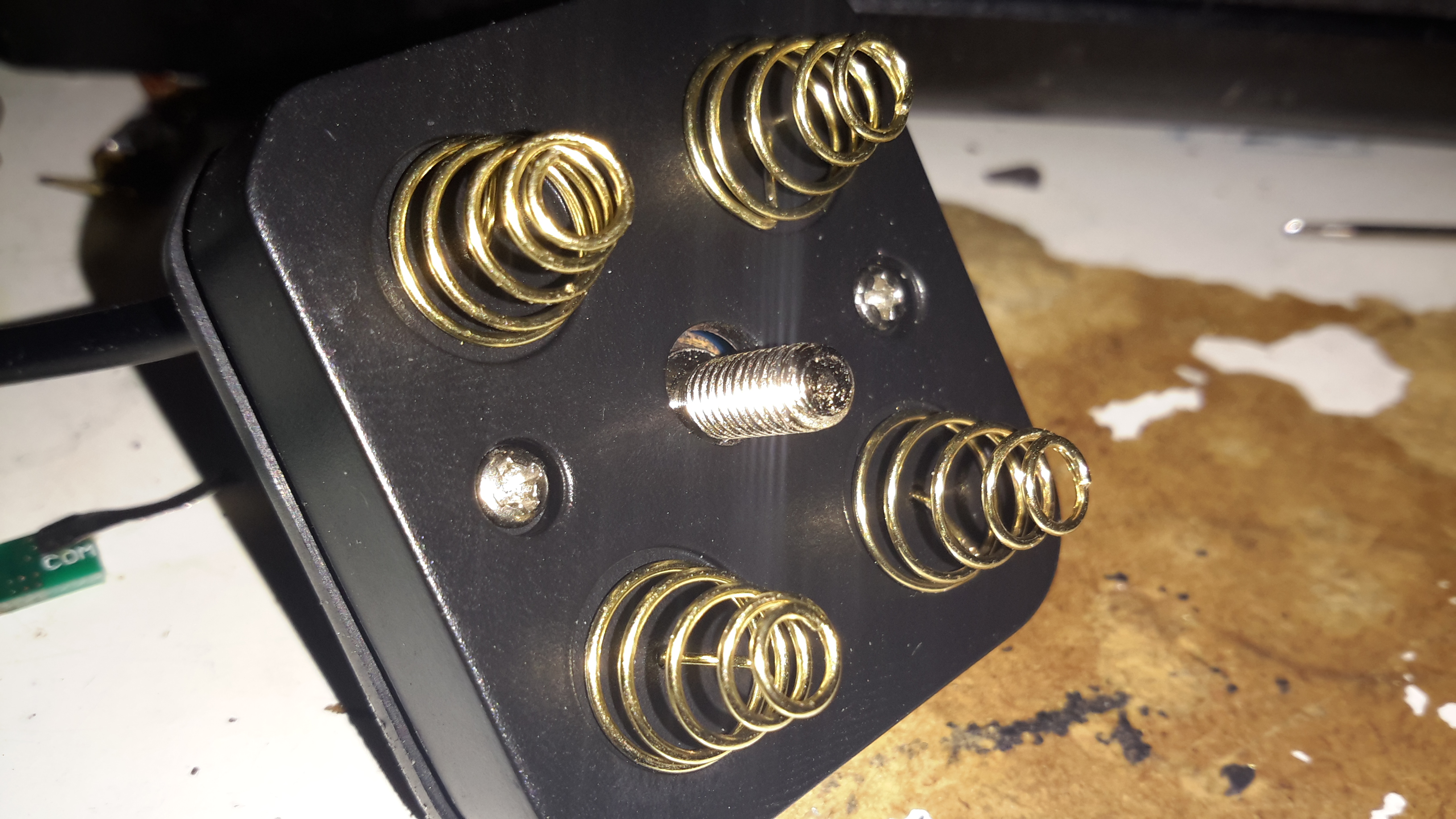
Cell Springs
The top cover holds the cell springs & the electronics.
Button & Cable Seal
Removing the pair of screws allows the top cap to open up. The cable, button & LEDs are robustly sealed off with this silicone moulding.
Top Removed
Here’s the PCB, not much on the top, other than the power button & battery indicator LEDs.
Electronics
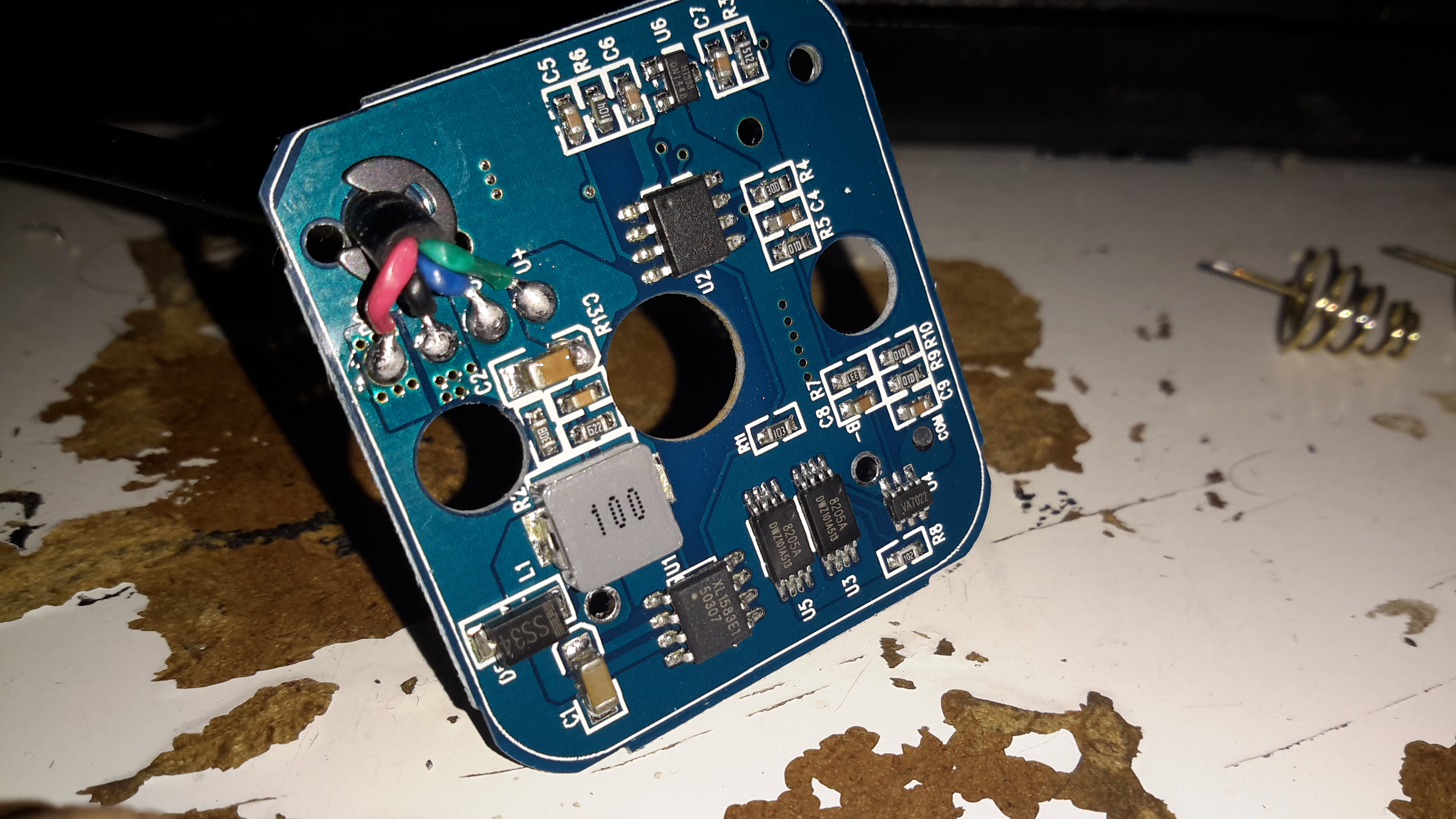
Desoldering the cell springs allows the PCB to pop out of the plastic moulding. There’s more than I expected here!
Bottom left is a DC-DC converter, generating the +5v rail for the USB port, this is driven with an XL1583 3A buck converter IC.
Bottom right is the protection IC & MOSFETs for the Lithium Ion cells. I wasn’t able to find a datasheet for the tiny VA7022 IC, but I did manage to make certain it was a 7.4v Li-Ion protection IC.
Top right is a completely unmarked IC, and a 3.3v SOT-23 voltage regulator. I’m assuming that the unmarked IC is a microcontroller of some sort, as it’s handling more than just the battery level LEDs.
A pretty decent 4-core cable finishes the job off. For once there’s actually some copper in this cable, not the usual Chineseuim thin-as-hair crap.
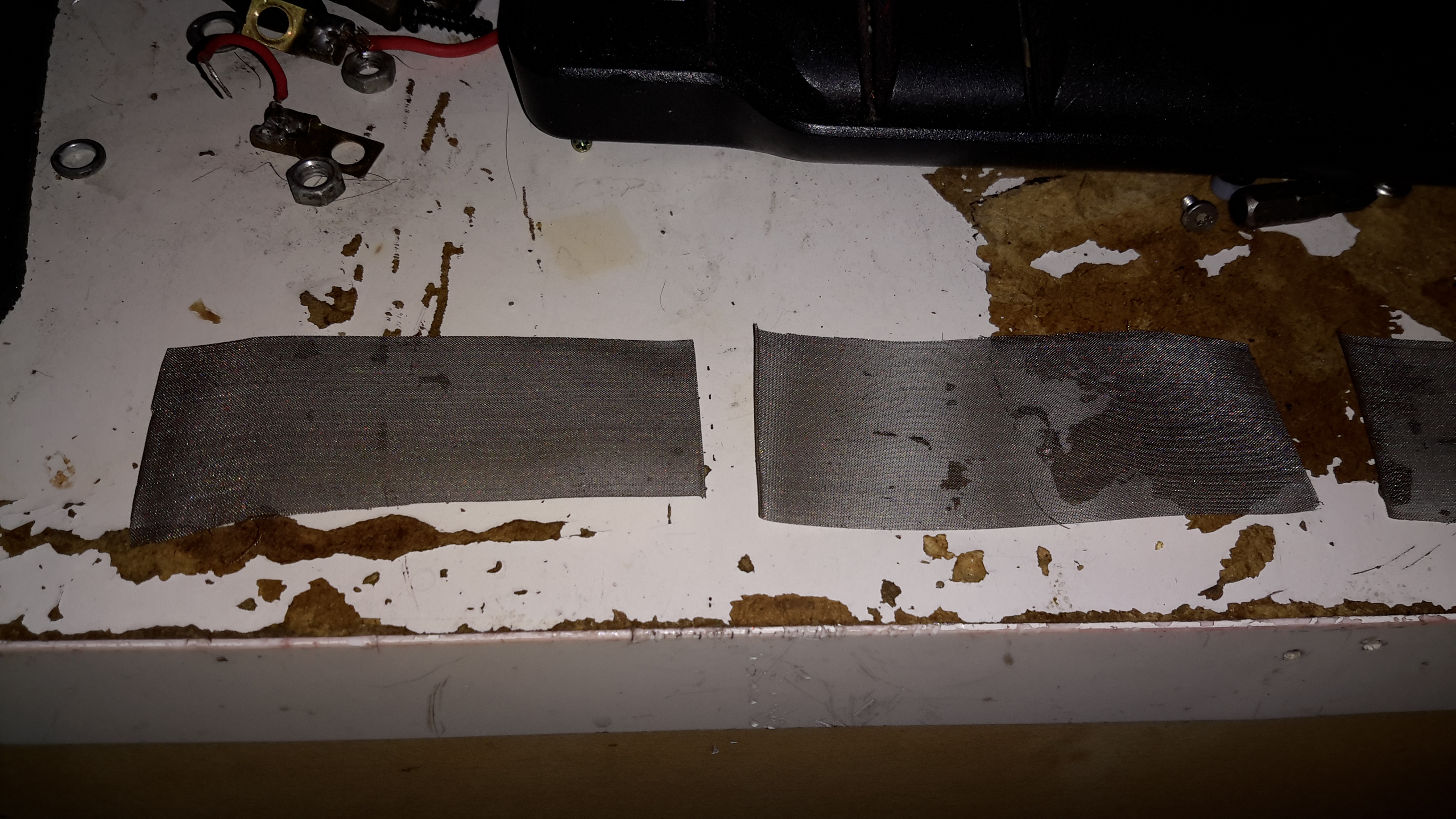
A while ago I posted about the glowplug screens in Eberspacher heaters, and making some DIY ones, as the OEM parts are hideously expensive for a piece of stainless mesh (£13).
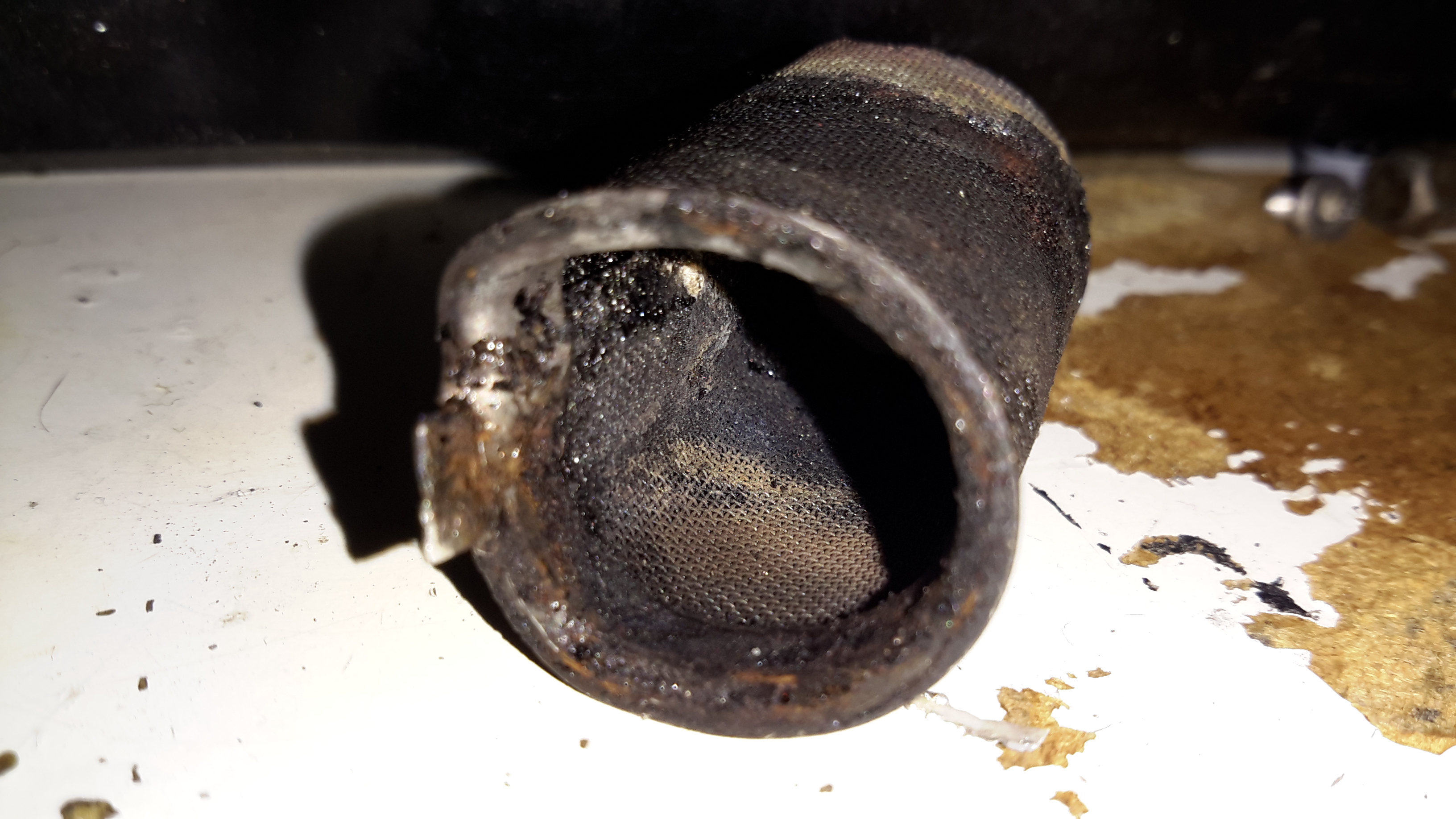
Old Screen
Above is the old factory screen that I extracted after only 5 gallons of diesel was run through it, it’s heavily clogged up with carbon & tar. The result of this clogging is a rather slow & smoky start of the heater & surging of the burner while at full power.
It wasn’t as badly stuck in the chamber as some I’ve removed, but extracting it still caused the steel ring to deform, this was after using a scalpel blade to scrape the carbon off the rim.
At the time I did some tests with some spare copper mesh I had to hand, but the problem with copper is that it’s very soft & malleable, so didn’t really hold it’s shape well enough. The factory screens are spot welded to keep them in shape, but as I don’t have a spot welder, I am relying on the mesh having a bit of springiness to keep it in place against the walls of the glowplug chamber.
eBay provided a piece of 120 mesh stainless steel mesh, 300mmx300mm for £8. It’s a bit finer than the stock stuff, but appears to work perfectly fine as long as there’s no gunk in the fuel to clog it up.
I cut a strip off the large piece, as wide as the OEM screen, about 32mm. This 300mm long strip is then cut into 4 pieces, each 75mm long. (it’s easily cut with scissors, but mind the stray wires on the edges! They’re very sharp & penetrate skin easily!).
Mesh Screen
These pieces are just the right size to form a complete loop in the glowplug chamber, and the stainless is springy enough so that it doesn’t deform & become loose.
The OEM screen is multiple turns of a more coarse mesh, but the finer mesh size of the screens I’m using means only one turn is required. Multiple turns would probably be too restrictive to fuel flow.
With one of these pieces of mesh in place, the heater starts instantly, without even a wisp of smoke from the exhaust. Burner surging is also eliminated. Even if the service life of my DIY replacement isn’t as long as an OEM screen, the low price for such a large number of replacements certainly offsets that disadvantage!
A piece of mesh from eBay would provide enough material for quite a lot of replacements, and probably more than the service life of the burner itself!
Here’s another Dyson teardown, in my efforts to understand how marketing have got hold of relatively simple technology & managed to charge extortionate amounts of money for it.
This is the DC35, the model after the introduction of the brushless digital motor.
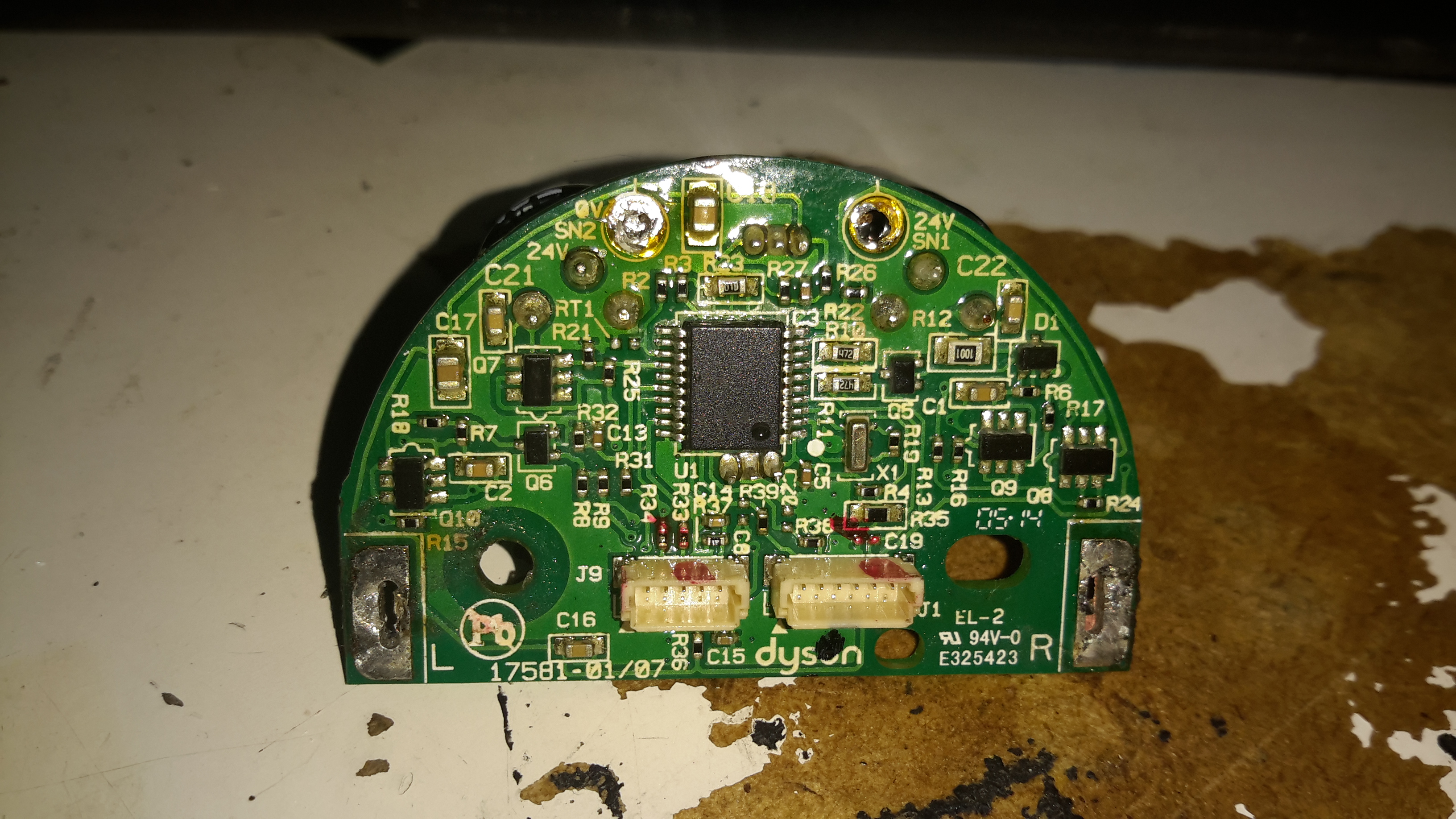
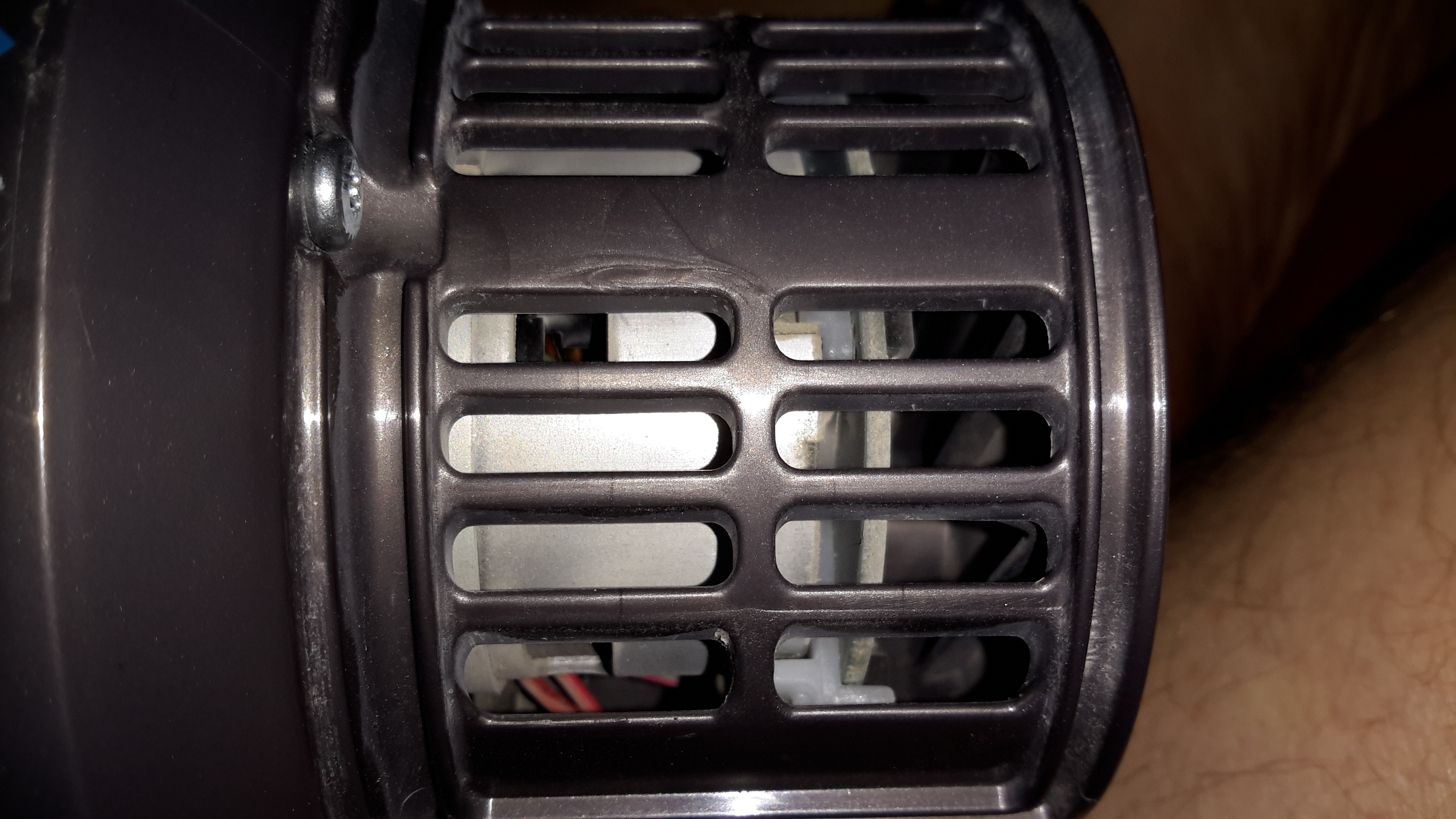
Back Cap Removed
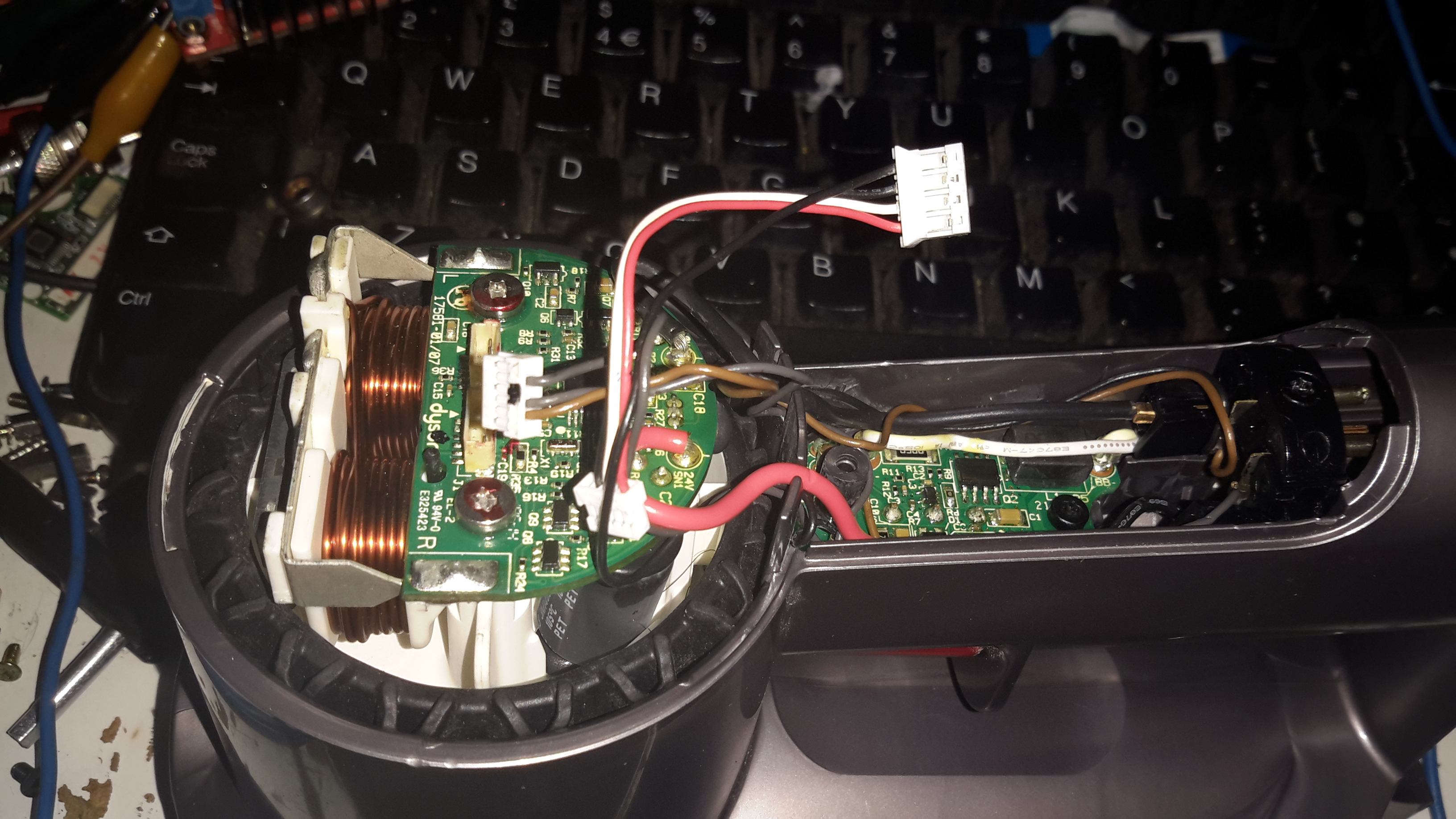
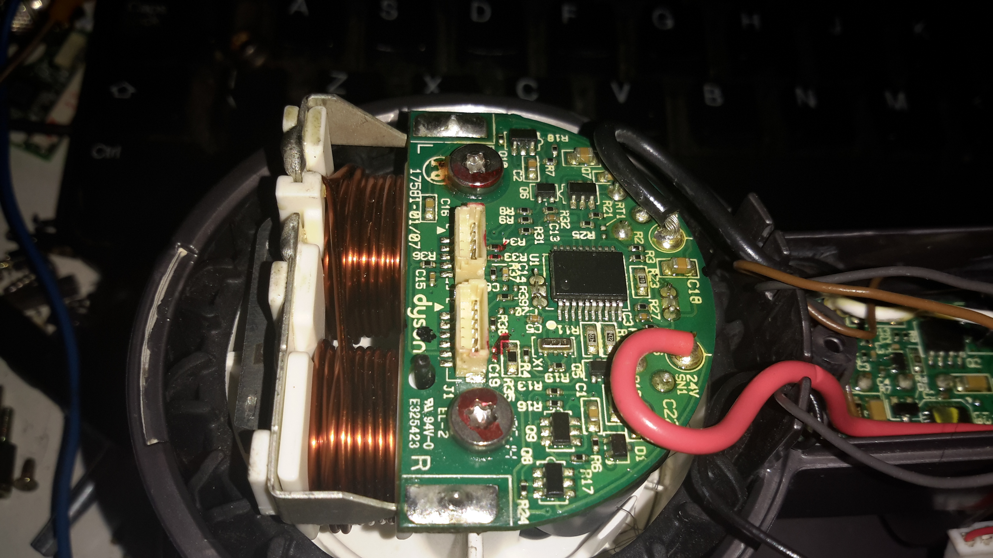
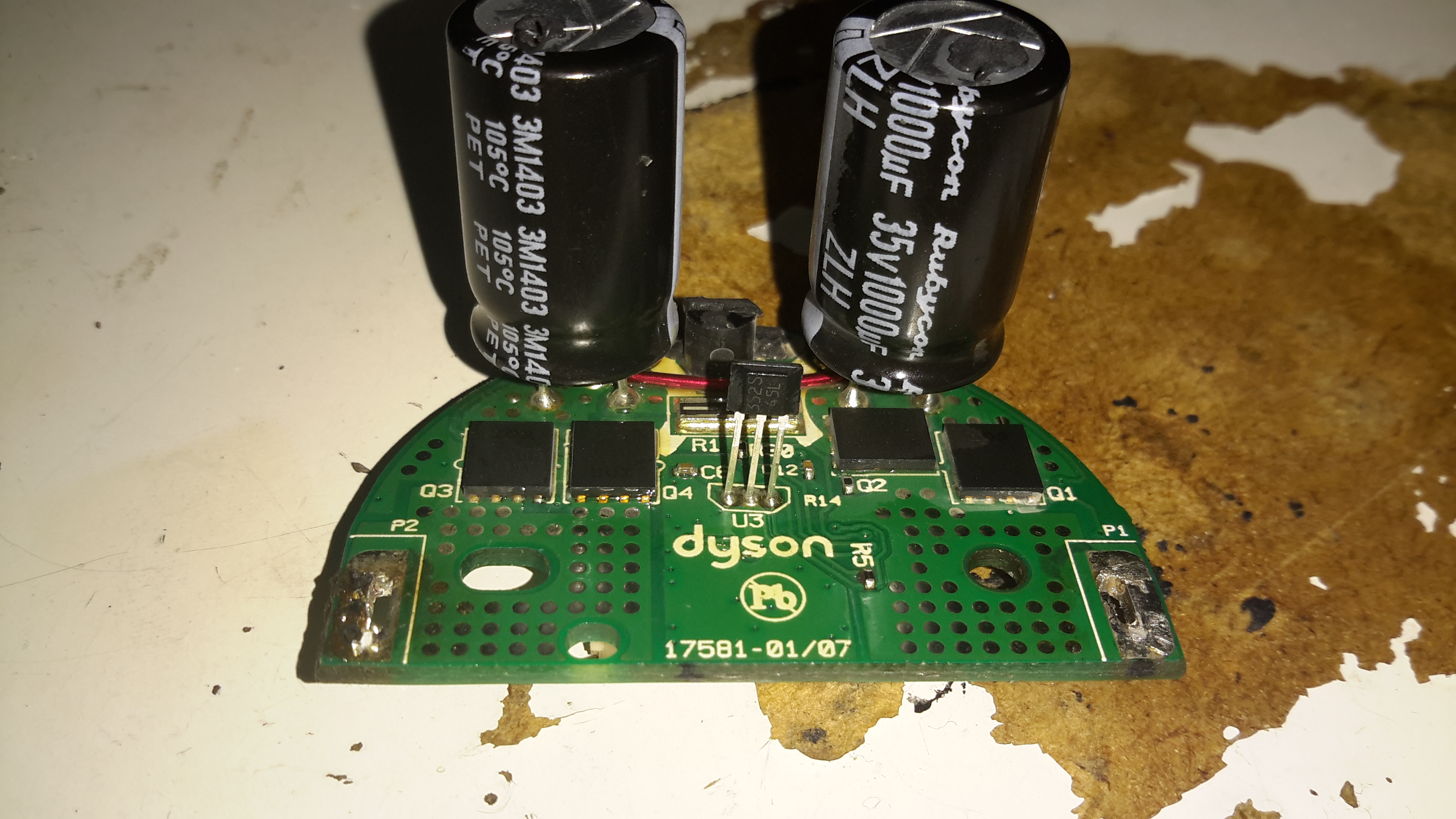
On this version the mouldings have been changed, and the back cover comes off, after removing the battery retaining screw. It’s attached with some fairly vicious clips, so some force is required. Once the cap is removed, all the electronics are visible. On the left is the motor itself, with it’s control & drive PCB. There’s another PCB on the trigger, with even more electronics. The battery connector is on the right.
Trigger PCB
Here’s the trigger PCB, which appears to deal with DC-DC conversion for powering the brush attachments. The QFN IC with yellow paint on it is an Atmel ATTiny461 8-bit microcontroller. This is probably controlling the DC-DC & might also be doing some battery authentication.
“Digital Motor”
Here’s the motor & it’s board. The windings on the stator are extremely heavy, which makes sense considering it’s rated at 200W. The main control IC is a PIC16F690 from Microchip. Instead of using an off the shelf controller, this no doubt contains software for generating the waveforms that drive the brushless motor. It also appears to communicate with the other PCBs for battery authentication.
Stator
Desoldering the board allows it to be removed from the motor itself. The pair of windings are connected in anti-phase, to create alternating North-South poles depending on polarity. Since the existing controller is unusable due to software authentication with the other parts, I might have a go at building my own driver circuit for this with an Arduino or similar.
Blower Assembly
The blower assembly is simple plastic mouldings, pressed together then solvent welded at the seam.
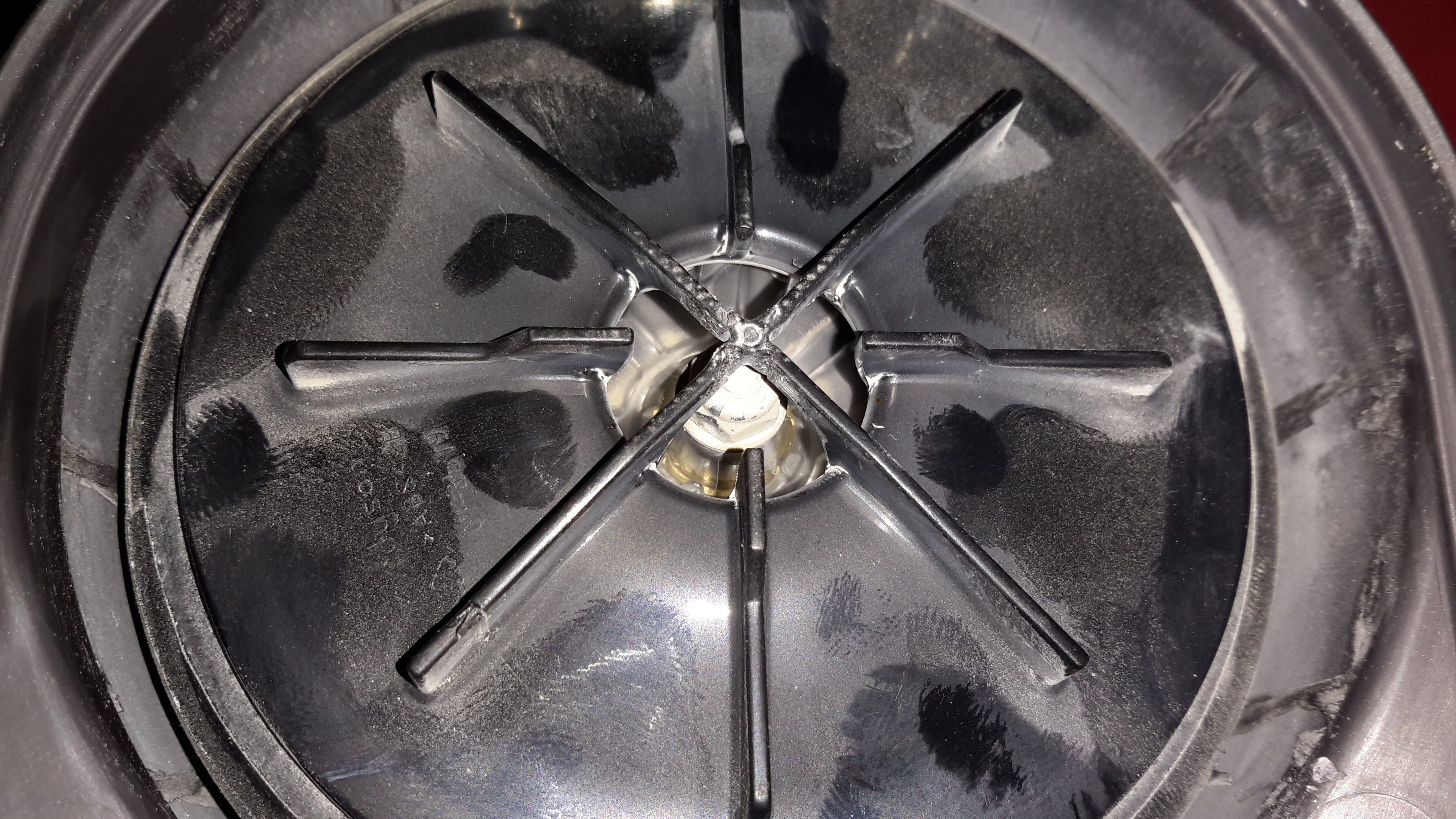
Impeller
The impeller is just a centrifugal compressor wheel, identical to what’s used in engine turbochargers.
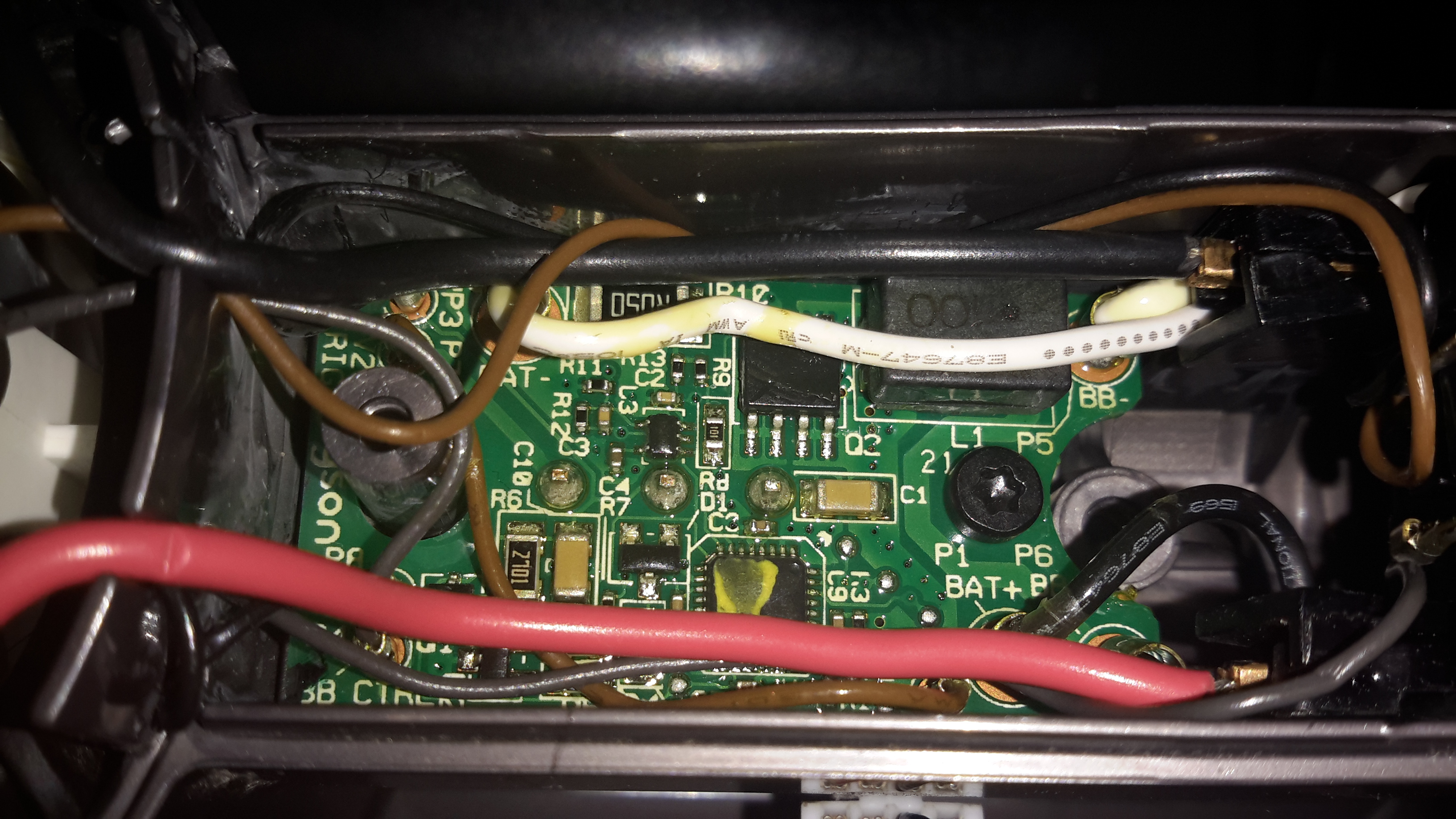
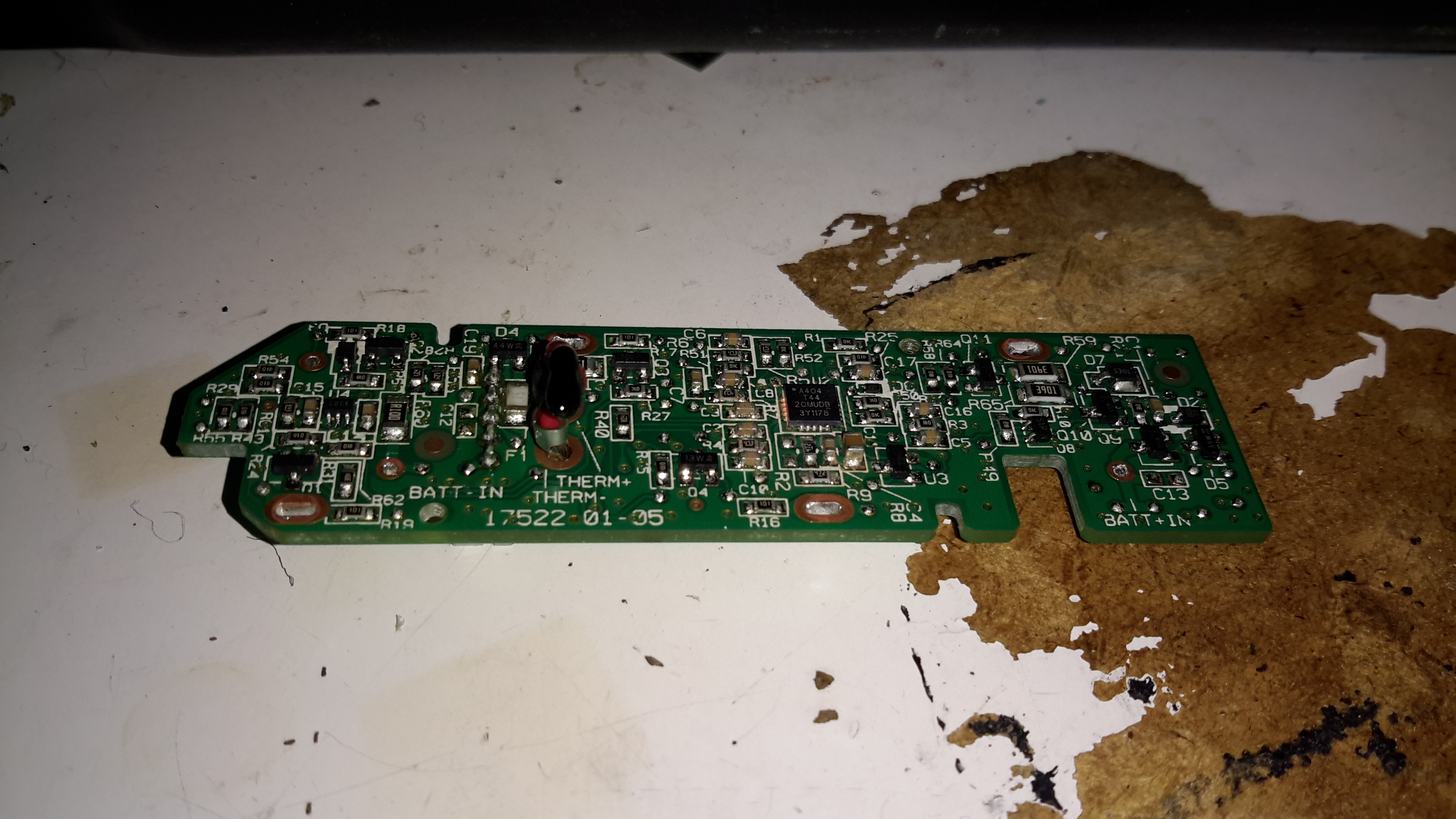
Motor Control Board
The inside face of the control PCB holds the 4 very large MOSFETs, IRFH7932PbF from International Rectifier. These are rated at 30v 20A a piece, and are probably wired in a H-Bridge. There’s a bipolar Hall switch to sense rotor position & rotation speed, and an enormous pair of capacitors on the main power bus.
Motor Control Board Reverse
Not much on the other side of the PCB other than the microcontroller and associated gate drive stuff for the FETs.
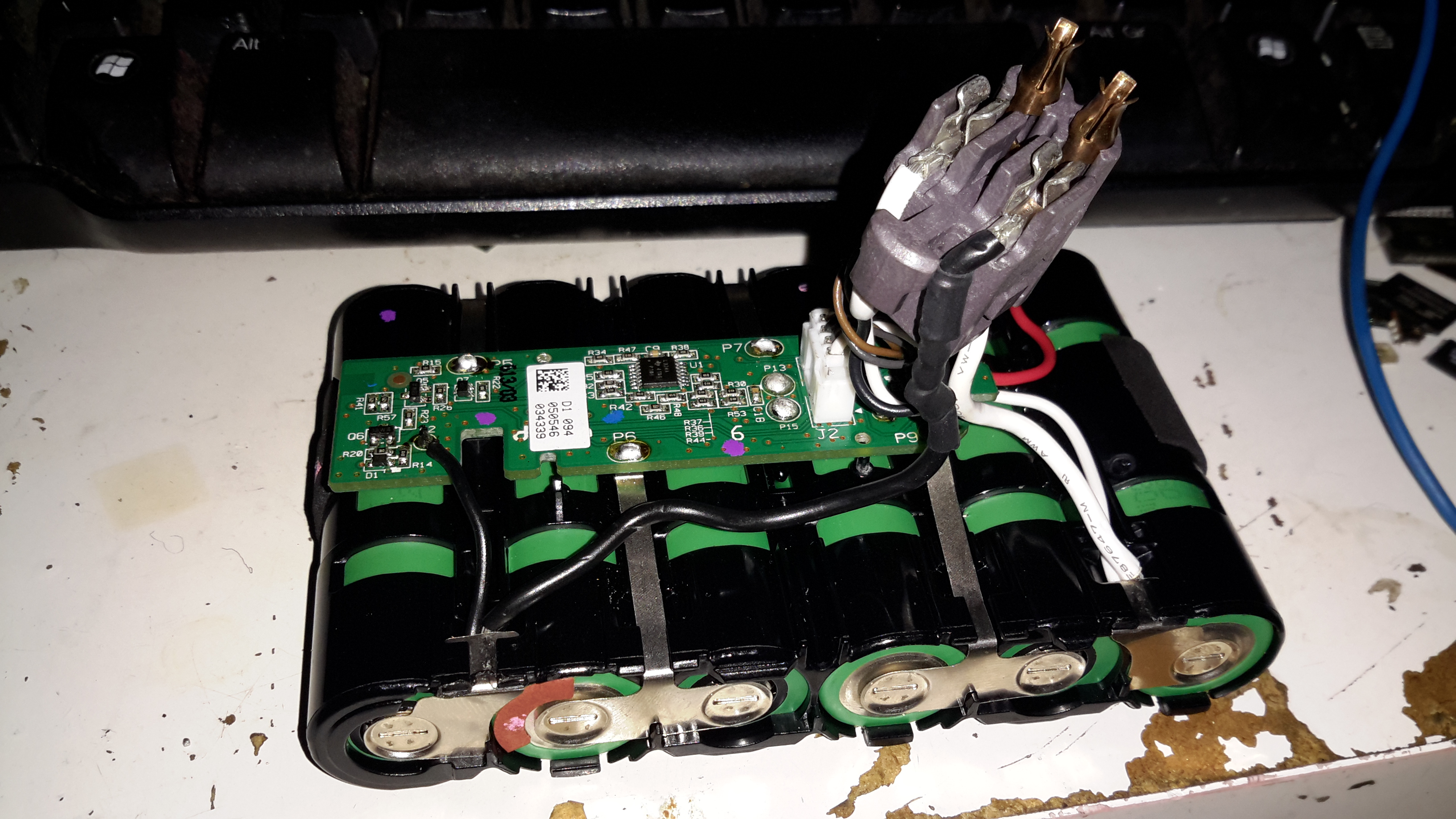
Battery Pack Opened
The battery pack is similar to the DC16 in it’s construction, a heavily clipped together plastic casing holding 6 lithium cells. In this one though there’s a full battery management system. The IC on the top of the board above is a quad Op-Amp, probably for measuring cell voltages.
Battery BMS Bottom
The other side of the BMS board is packed with components. I wasn’t able to identify the QFN IC here, as it’s got a custom part number, but it’s most definitely communicating with the main motor MCU via I²C over the two small terminals on the battery connector.
Since this is the 300th post on my blog in the 6 years I’ve been at this, I figured I’d do a post with recent site updates & some news.
Site Look
There haven’t been many updates to the general look of the site for quite a while, with some help of a friend I managed to get a new ticker added to the header, which saves on post count for upcoming projects & posts.
The header image is also dynamic, picking randomly from a collection of images, mostly from previous posts, and a few that started as messing about with a camera & turned out looking quite good.
Site Support
Also added to the site’s look is a Tip Jar on the right hand side, so thankful readers can donate something if I’ve managed to post something remotely helpful ;).
People that know me personally know I hate ads with a passion, and as such ads will have no place on my blog for as long as it’s visible on the intertubes. The site does cost quite a significant (to me anyway) amount of cash to keep going, not to mention time, so any donations would be more than welcome!
Radio-Based Posts
I haven’t done any proper Ham Radio based posts in quite a while, mainly due to me not having anything to share on the subject, unfortunately it can be a damn expensive hobby & there are other things taking priority at the moment. (Apparently eating & warmth are essentials, according to the missus at least ;)).
There is going to be a round-about radio based post shortly though, so my Ham readers stay tuned!
Boating Posts
Now that we’re in the new year, when the weather returns to something remotely tolerable to be outdoors in, there’ll be much more boating related stuff on the cards, not only trips but engineering jobs onboard.
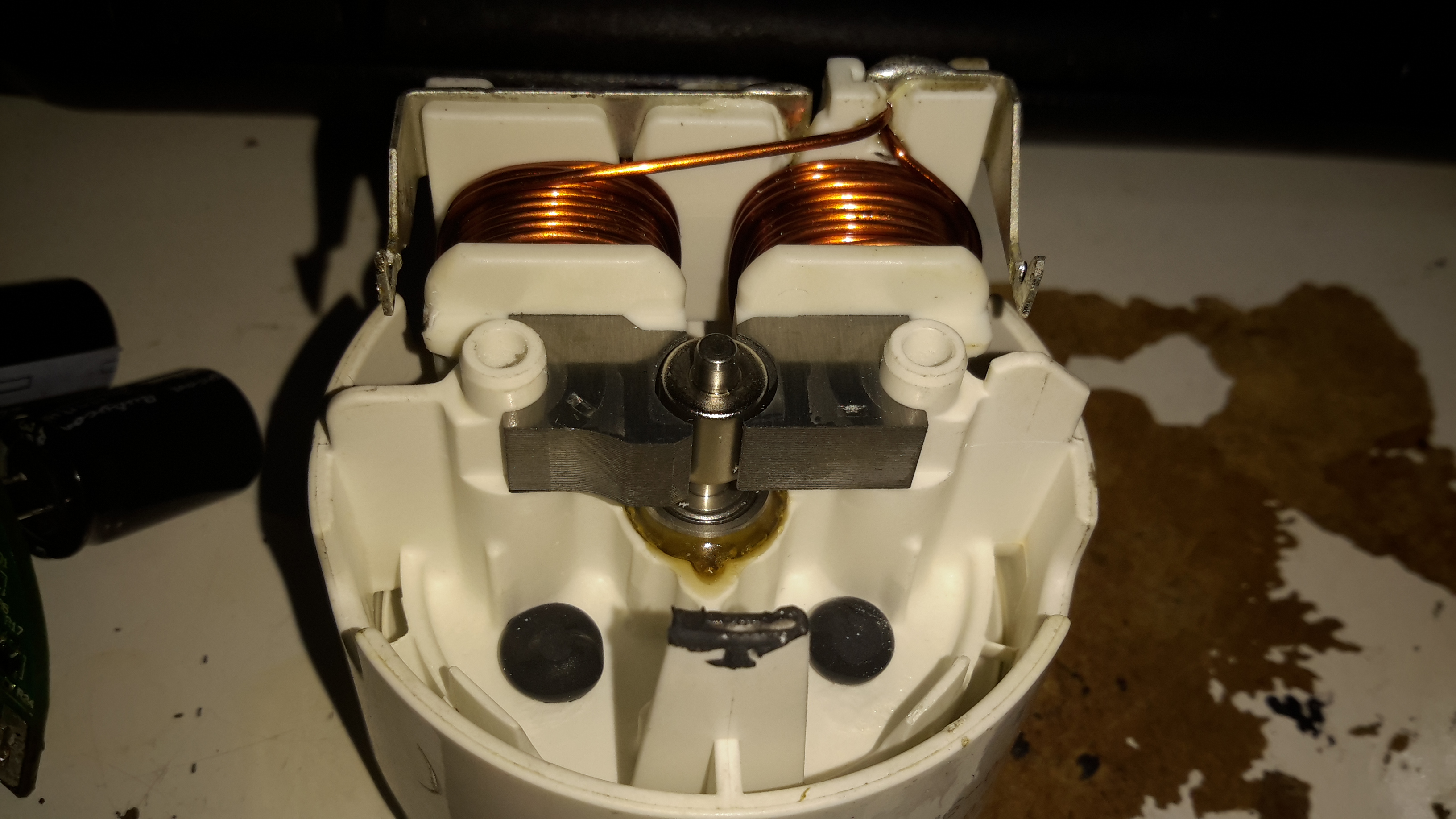
The Dyson DC16 is one of the older handheld vacuums, before the introduction of the “Digital Motor”. (Marketing obviously didn’t think “Switched Reluctance Motor” sounded quite as good).
These vacuums have a very large DC brush motor driving the suction turbine instead, the same as would be found in a cordless power tool.
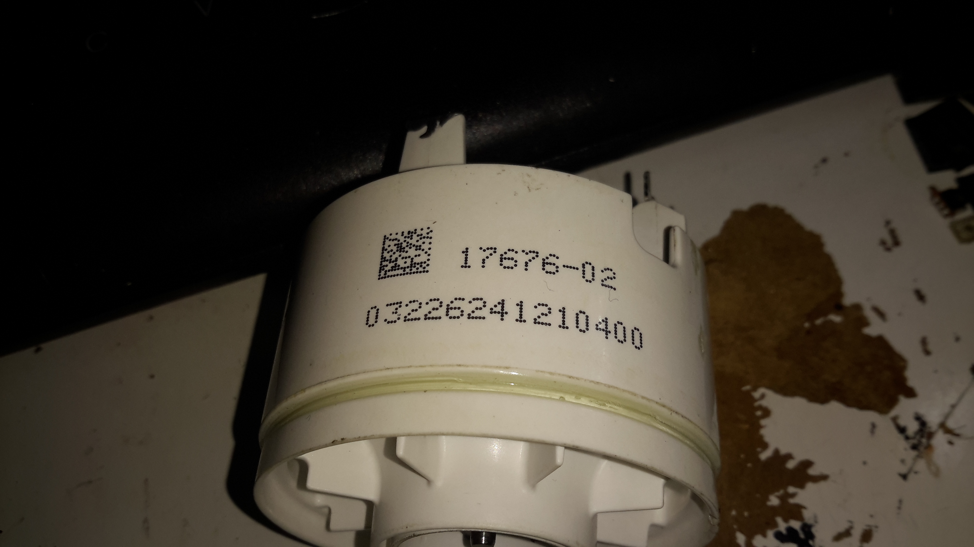
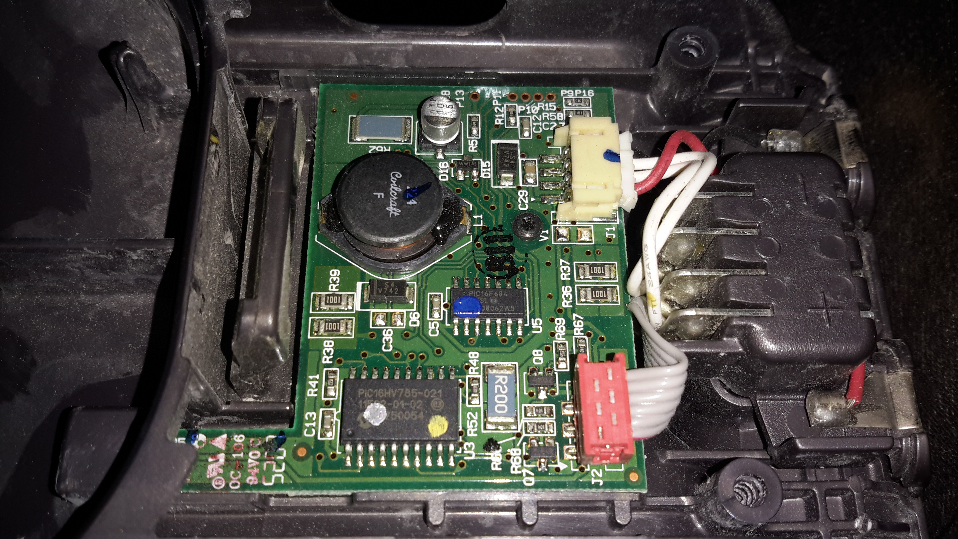
Control PCB
Popping the front cap off with the ID label, reveals the brains of the vacuum. The two large terminals at the right are for charging, which is only done at 550mA (0.5C). There are two PIC microcontrollers in here, along with a large choke, DC-DC converter for supplying the logic most likely. The larger of the MCUs, a PIC16HV785, is probably doing the soft-start PWM on the main motor, the smaller of the two, a PIC16F684 I’m sure is doing battery charging & power management. The motor has a PCB on it’s tail end, with a very large MOSFET, a pair of heavy leads connect directly from the battery connector to the motor.
Just out of sight on the bottom left edge of the board is a Hall Effect Sensor, this detects the presence of the filter by means of a small magnet, the vacuum will not start without a filter fitted.
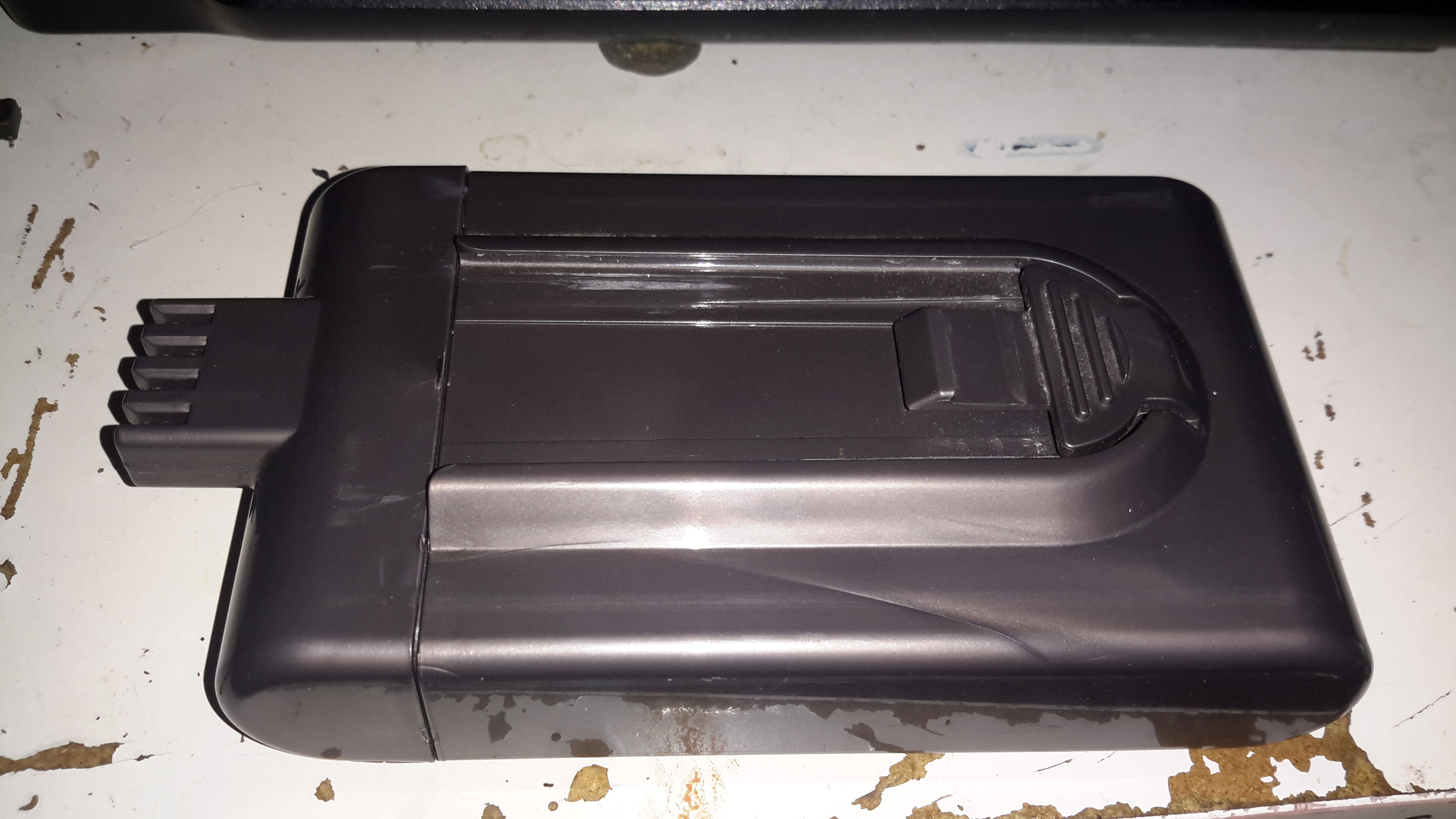
Battery Pack
The battery pack is a large custom job, obviously. 4 terminals mean there’s slightly more in here than just the cells.
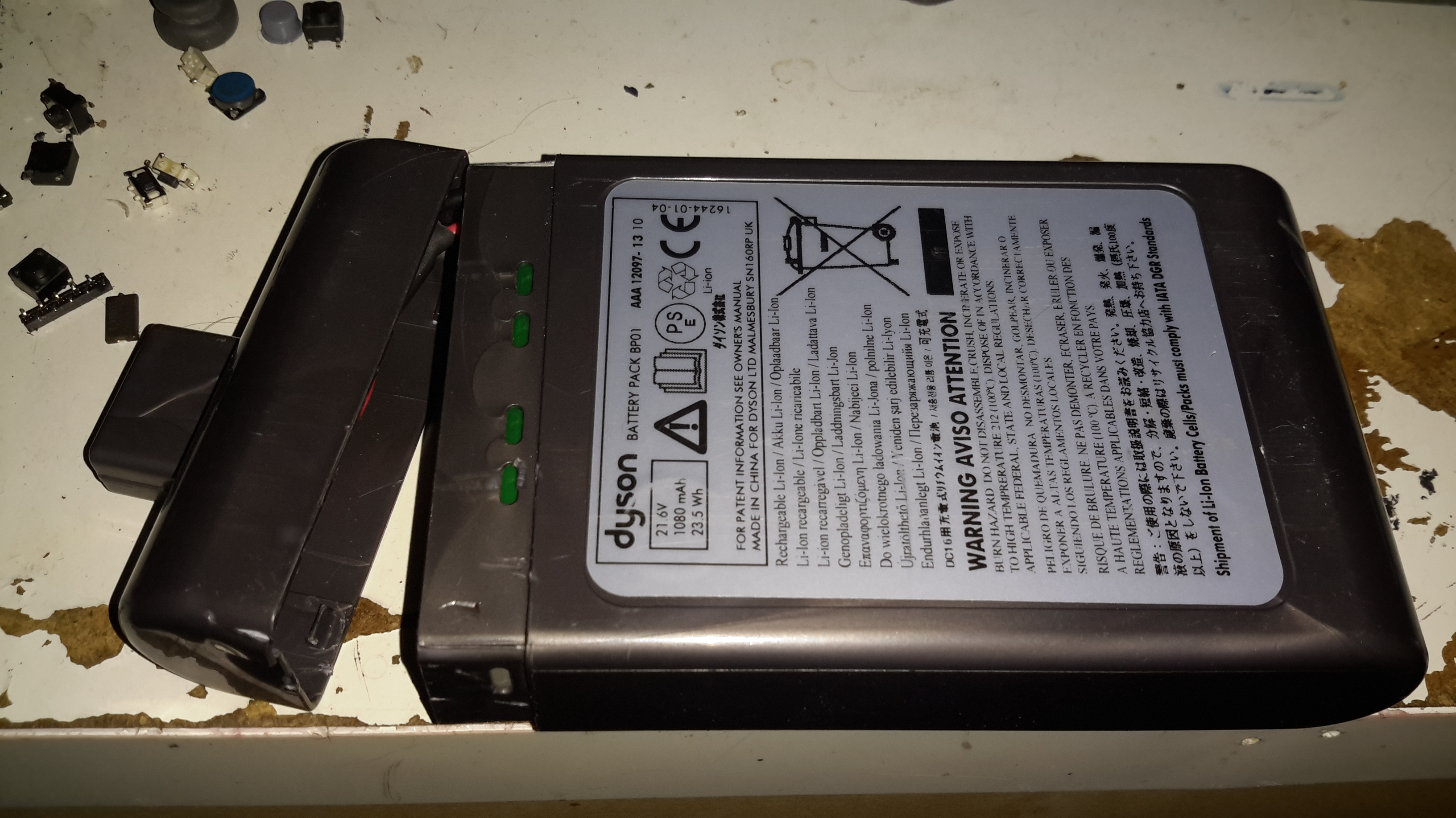
Battery Cracked
Luckily, instead of ultrasonic or solvent welding the case, these Dyson batteries are just snapped together. Some mild attack with a pair of screwdrivers allows the end cap to be removed with minimal damage.
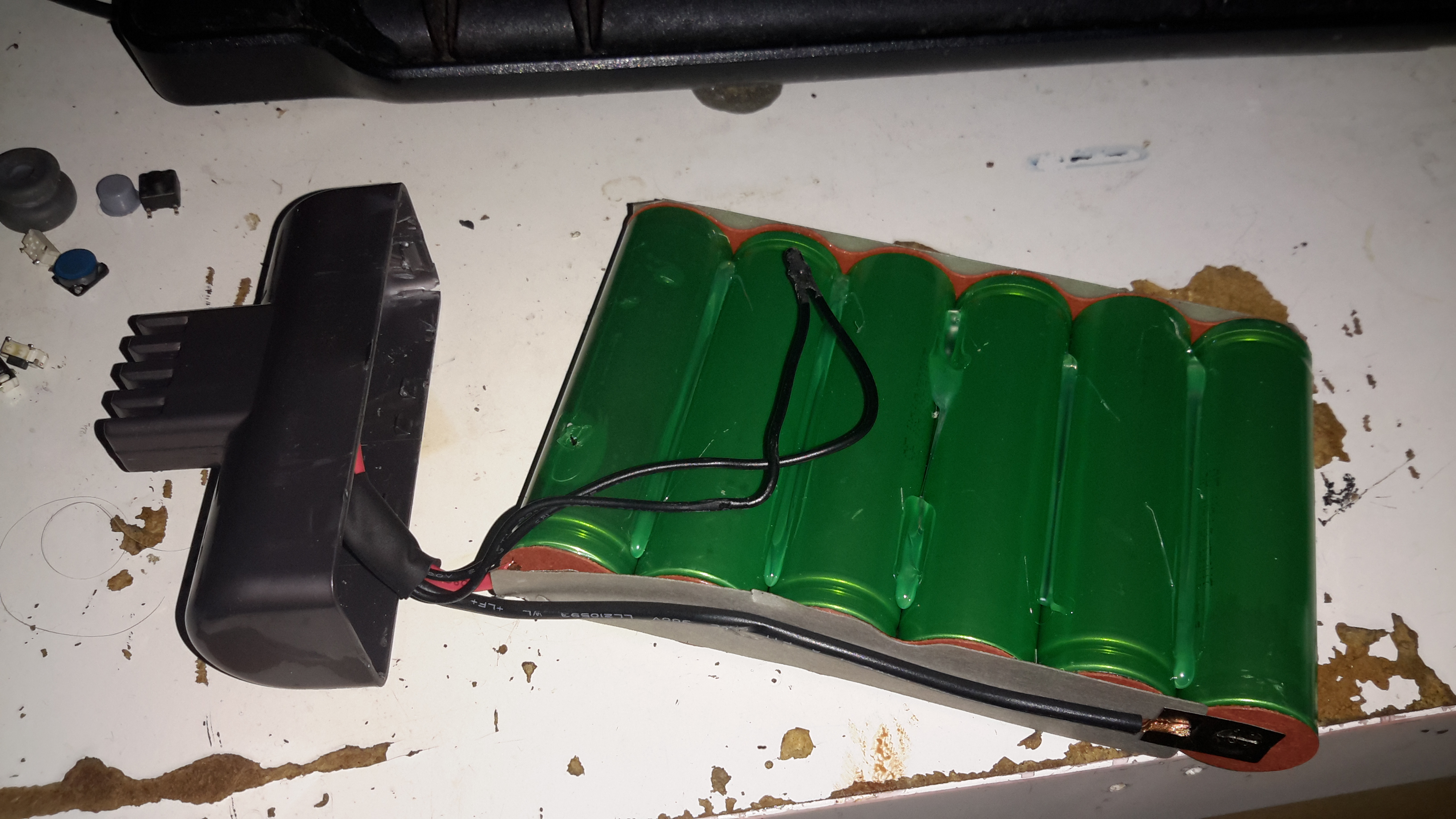
Cells
The cells were lightly hot-glued into the shell, but that can easily be solved with a drop of Isopropanol to dissolve the glue bond. The pack itself is made up of 6 Sony US18650VT High-Drain 18650 Li-Ion cells in series for 21.6v nominal. These are rated at a max of 20A discharge current, 10A charge current, and 1.3Ah capacity nominal.
There’s no intelligence in this battery pack, the extra pair of terminals are for a thermistor, so the PIC in the main body knows what temperature the pack is at – it certainly gets warm while in use due to the high current draw.
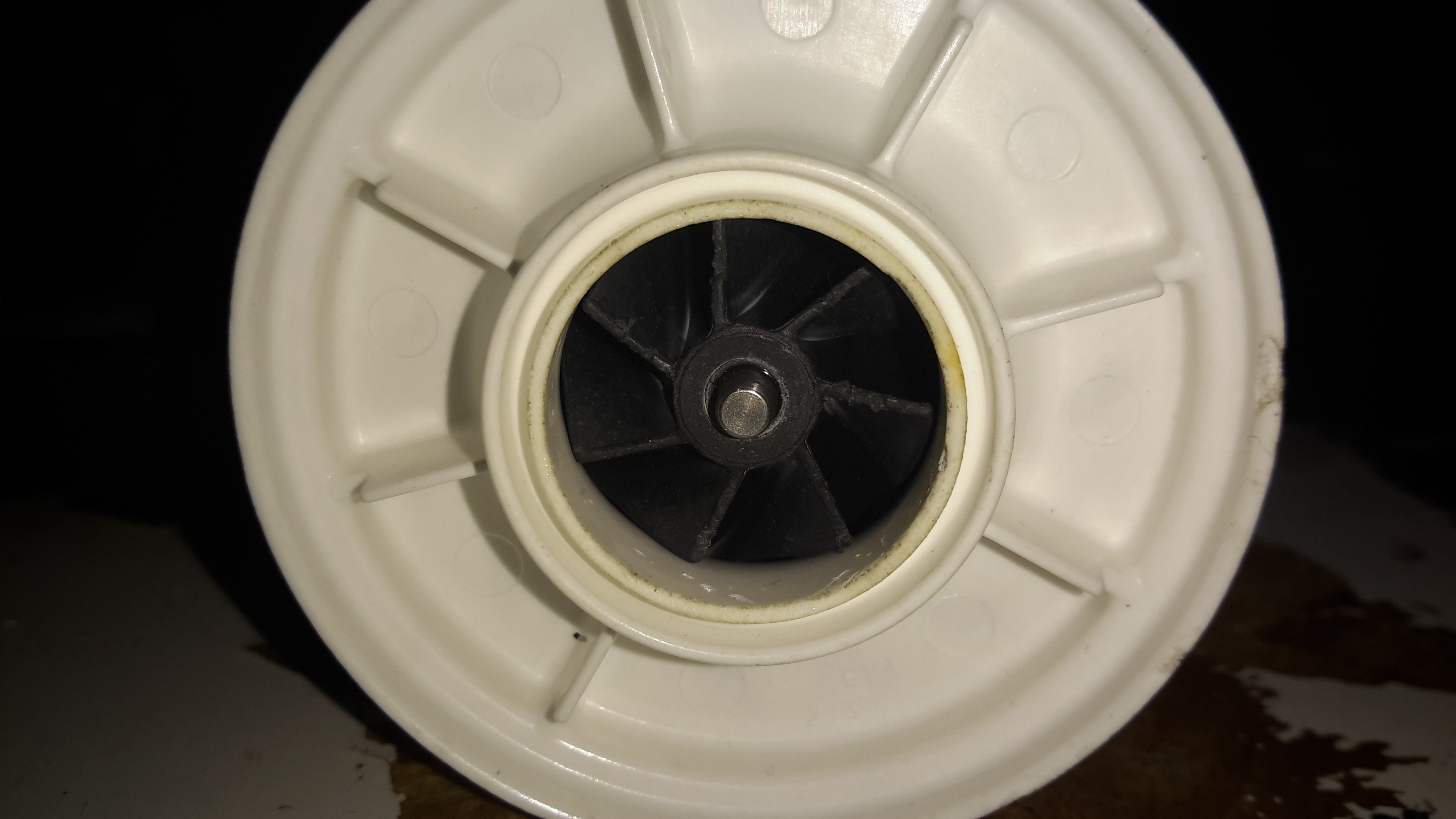
Motor
Hidden in the back side of the main body is the motor. Unfortunately I wasn’t able to get this out without doing some damage, as the wiring isn’t long enough to free the unit without some surgery.
Turbine
The suction is generated by a smaller version of the centrifugal high-speed blowers used in full size vacuums. Not much to see here.
Unofficial Charger
Since I got this without a charger, I had to improvise. The factory power supply is just a 28v power brick, all the charging logic is in the vacuum itself, so I didn’t have to worry about such nasties as over-charging. I have since fitted the battery pack with a standard Li-Po balance cable, so it can be used with my ProCell charger, which will charge the pack in 35 minutes, instead of the 3 hours of the original charger.
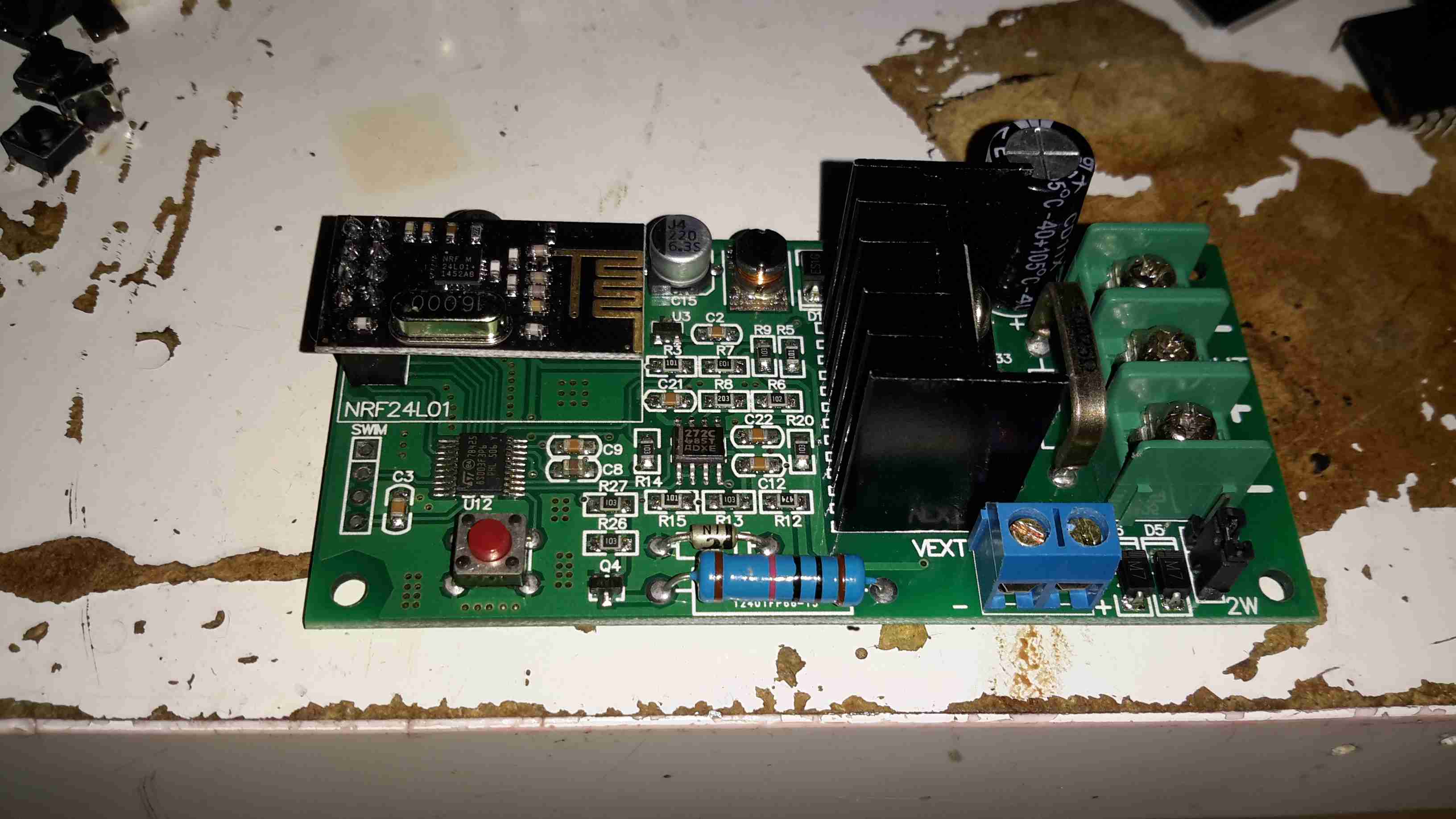
I recently came across these on eBay, so I thought I’d grab one to see how they function, with all the metrics they display, there’s potential here for them to be very useful indeed.
One of the best parts is that no wiring is required between the sensor board & the LCD head unit – everything is transmitted over a 2.4GHz data link using NRF24L01 modules.
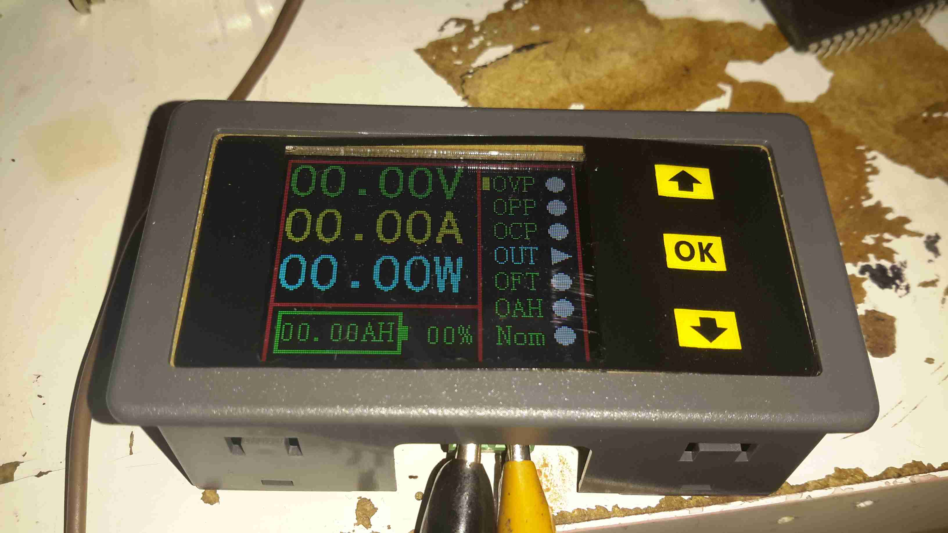
Above is the display unit, with it’s colour LCD display. Many features are available on this, & they appear to be designed for battery powered systems.
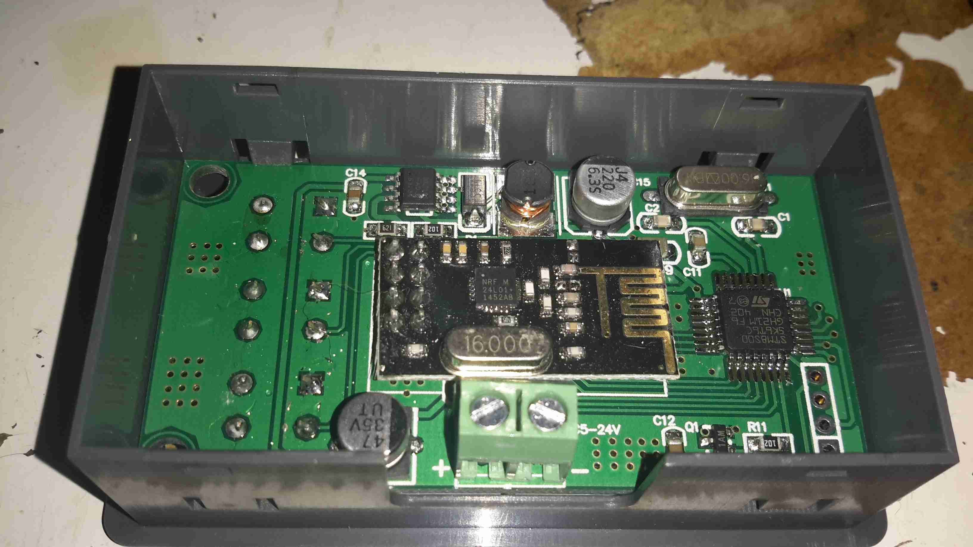
Monitor PCB
Another PCB handles the current & voltage sensing, so this one can be mounted as close to the high current wiring as possible.
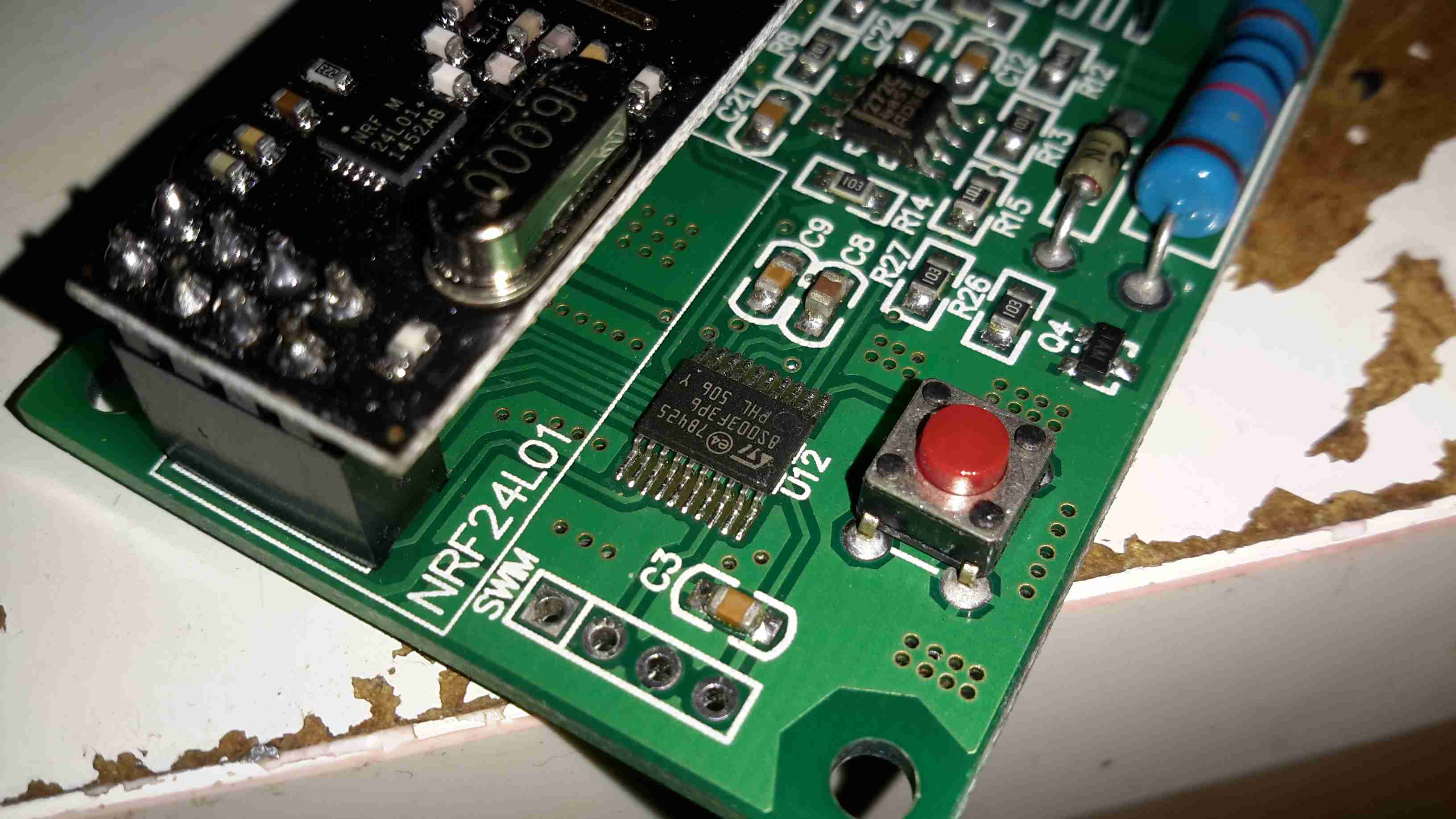
Monitor PCB Microcontroller
The transmitter PCB is controlled with an STM8S003F3 microcontroller from ST Microelectronics. This is a Flash based STM with 8KB of ROM, 1KB of RAM & 10-bit ADC. The NRF24L01 transceiver module is just to the left.
There’s only a single button on this board, for pairing both ends of the link.
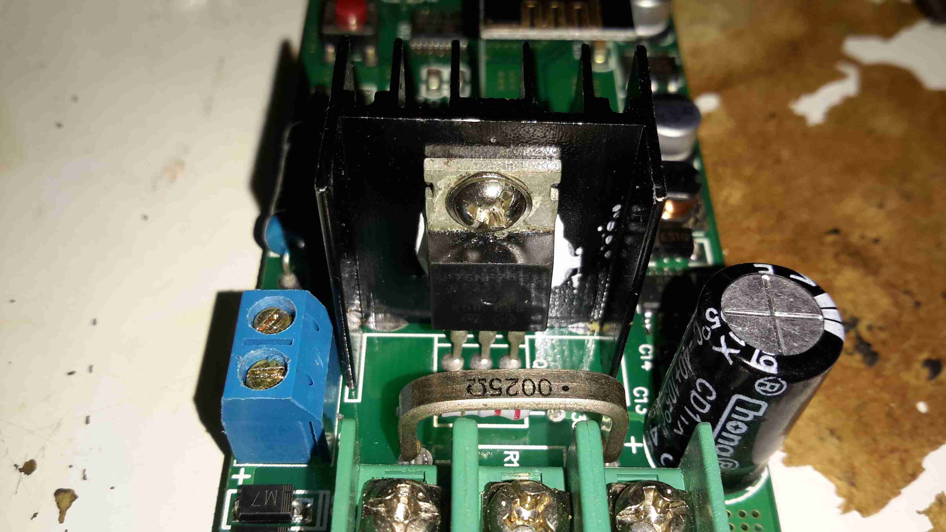
Output MOSFET
The high current end of the board has the 0.0025Ω current shunt & the output switch MOSFET, a STP75NF75 75v 75A FET, also from ST Microelectronics. A separate power source can be provided for the logic via the blue terminal block instead of powering from the source being measured.
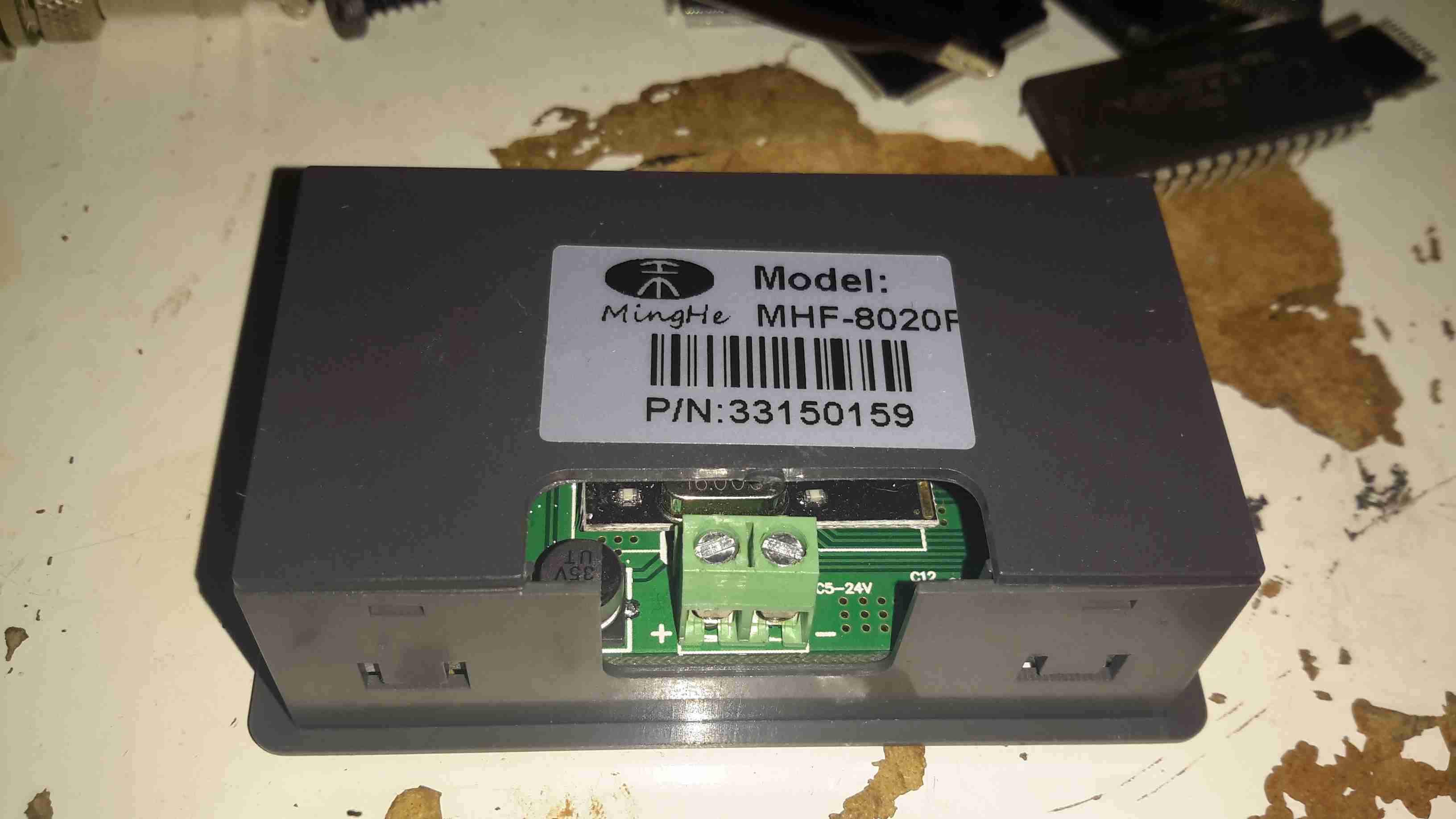
LCD Unit Rear
Here’s the display unit, only a pair of power terminals are provided, 5-24v wide-range input is catered for.
LCD Unit PCB
Unclipping the back of the board reveals the PCB, with another 2.4GHz NRF24L01 module, and a STM8S005K6 microcontroller in this case. The switching power supply that handles the wide input voltage is along the top edge of the board.
Unfortunately I didn’t get any instruction manual with this, so some guesswork & translation of the finest Chinglish was required to get my head round the way everything works. To make life a little easier for others that might have this issue, here’s a list of functions & how to make them work.
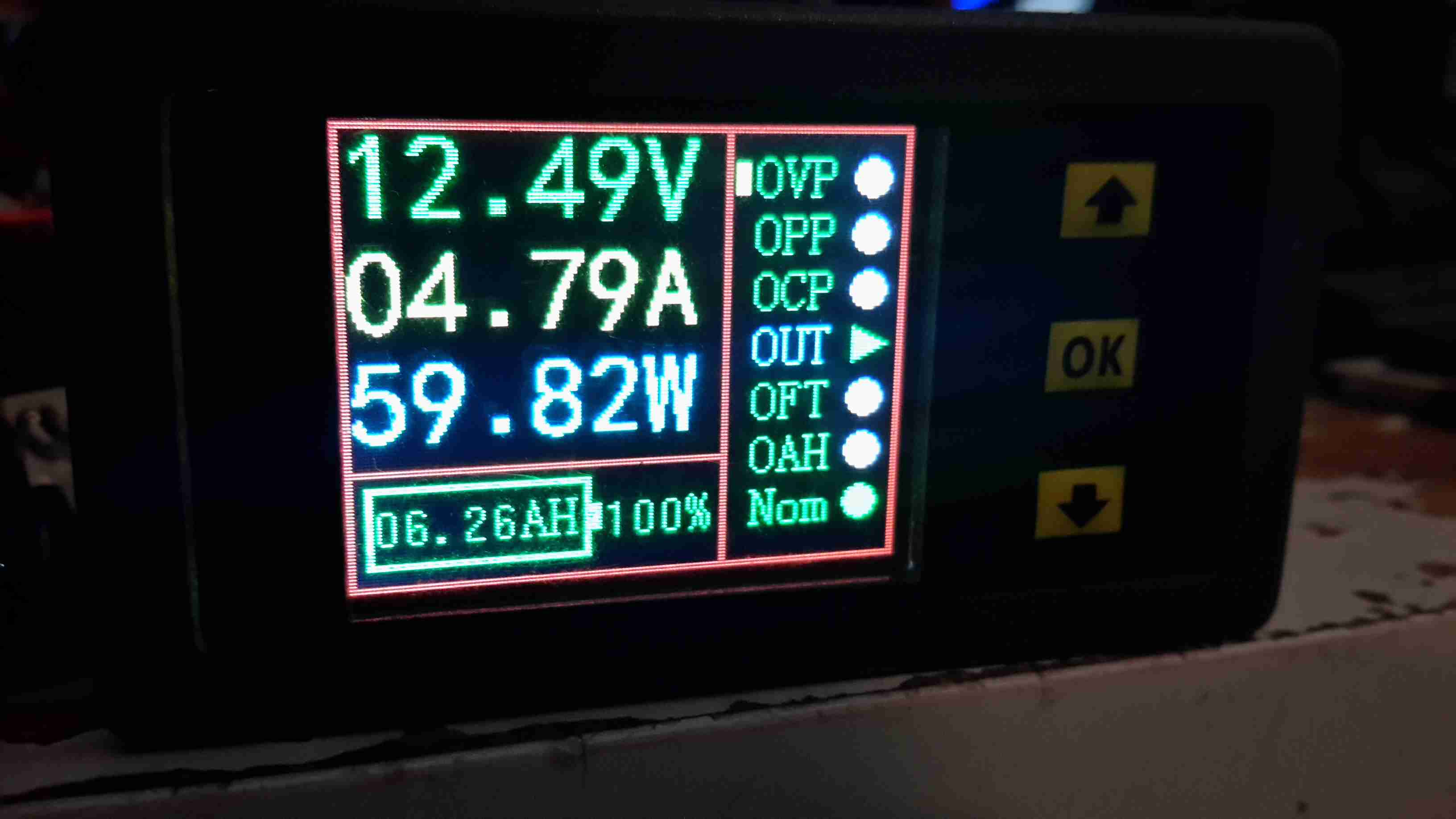
LCD Closeup
On the right edge of the board is the function list, a quick press of the OK button turns a function ON/OFF, while holding it allows the threshold to be set.
When the output is disabled by one of the protection functions, turning that function OFF will immediately enable the output again.
The UP/DOWN buttons obviously function to select the desired function with the cursor just to the left of the labels. Less obviously though, pressing the UP button while the very top function is selected will change the Amp-Hours display to a battery capacity icon, while pressing DOWN while the very bottom function is selected will change the Watts display to Hours.
The round circle to the right displays the status of a function. Green for OK/ON Grey for FAULT/OFF.
OVP: Over voltage protection. This will turn off the load when the measured voltage exceeds the set threshold.
OPP: Over power protection. This function prevents a load from pulling more than a specified number of watts from the supply.
OCP: Over current protection. This one’s a little more obvious, it’ll disable the output when the current measured exceeds the specified limit.
OUT: This one is the status of the output MOSFET. Can also be used to manually enable/disable the output.
OFT: Over time protection. This one could be useful when charging batteries, if the output is enabled for longer than the specified time, the output will toggle off.
OAH: Over Amp-Hours protection. If the counted Amp-Hours exceeds the set limit, the output will be disabled.
Nom: This one indicates the status of the RF data link between the modules, and can be used to set the channel they operate on.
Pairing is achieved by holding the OK button, selecting the channel on the LCD unit, and then pressing the button on the transmitter board. After a few seconds, (it appears to scan through all addresses until it gets a response) the display will resume updating.
This function would be required if there are more than a single meter within RF range of each other.
I’ve not yet had a proper play with all the protection functions, but a quick mess with the OVP setting proved it was very over-sensitive. Setting the protection voltage to 15v triggered the protection with the measured voltage between 12.5v-13.8v. More experimentation is required here I think, but as I plan to just use these for power monitoring, I’ll most likely leave all the advanced functions disabled.
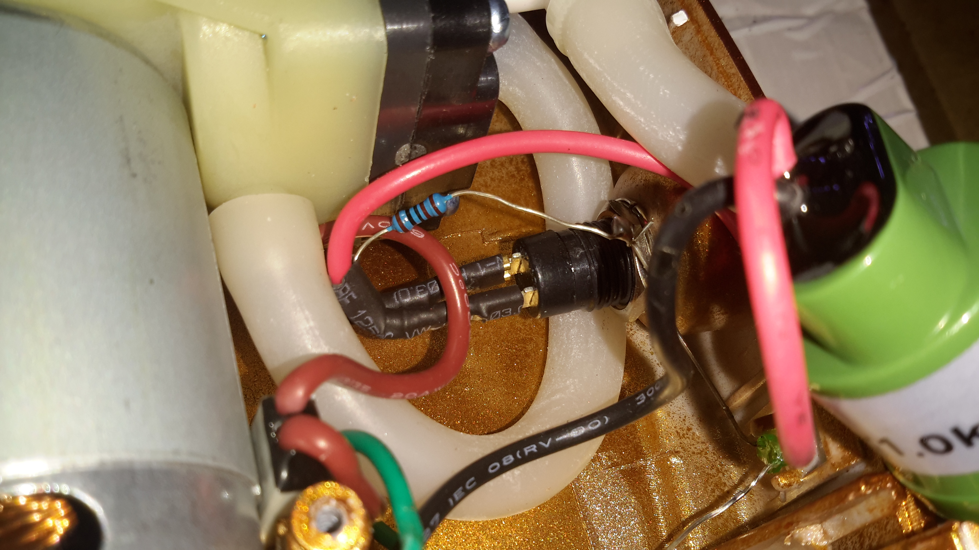
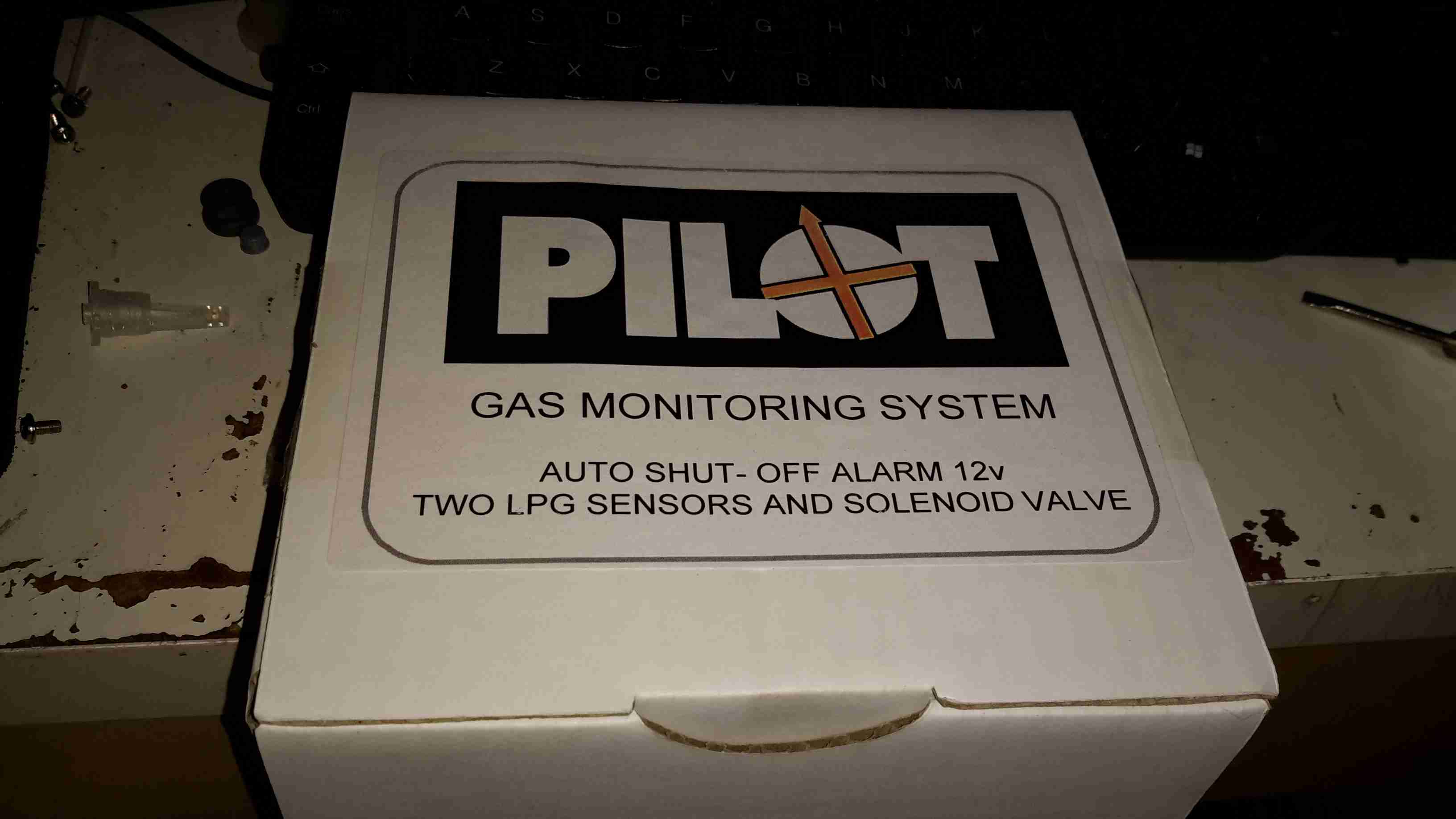
In my mind, the most dangerous thing onboard any boat is the LPG system, as the gas is heavier than air, any leaks tend to collect in the bilges, just waiting for an ignition source. To mitigate this possibility, we’re fitting a gas monitoring system that will sound an alarm & cut off the supply in case of a leak.
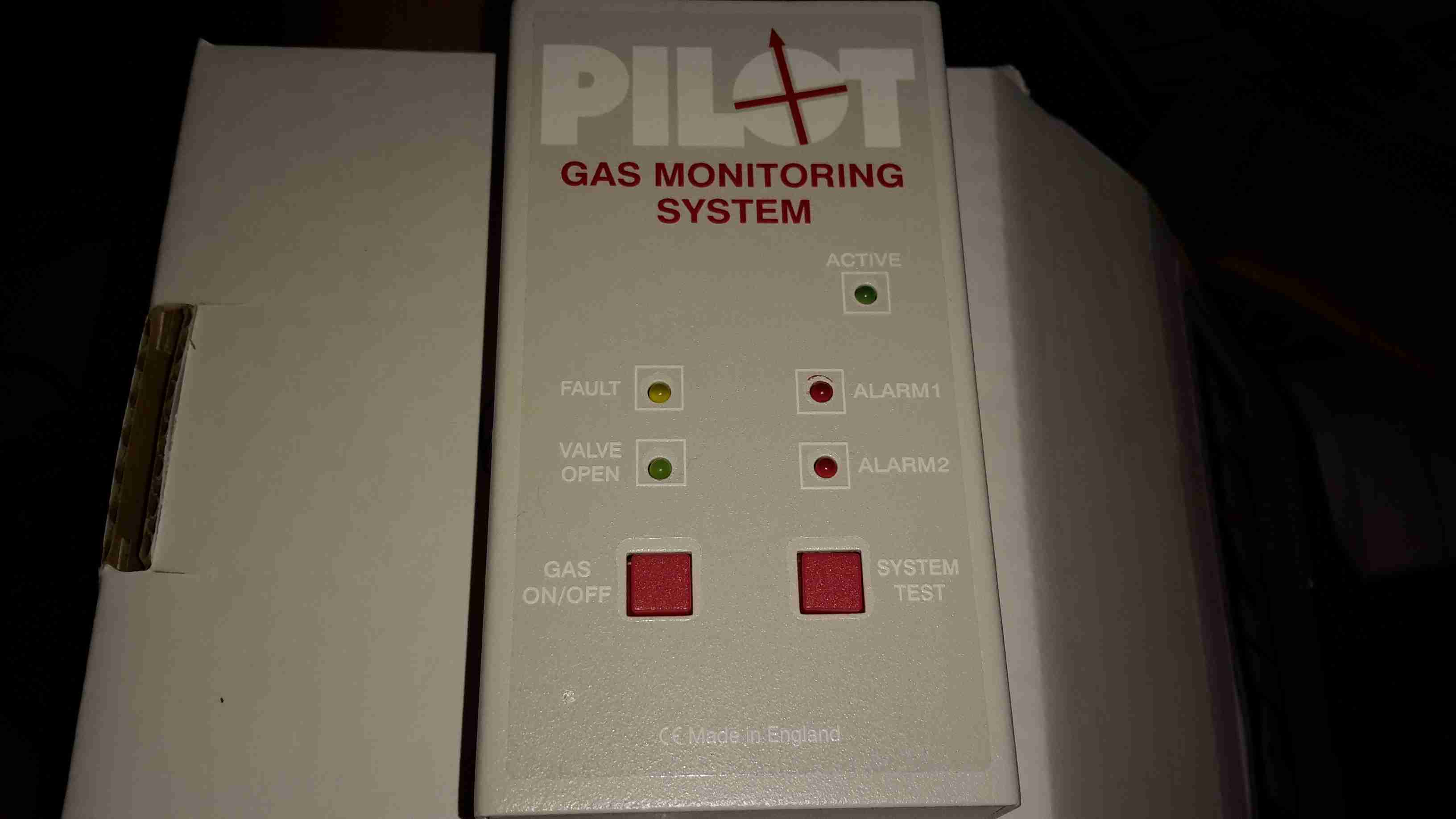
Monitor Unit
Here’s the monitor itself, the two sensor model. It’s nice & compact, and the alarm is loud enough to wake the dead.
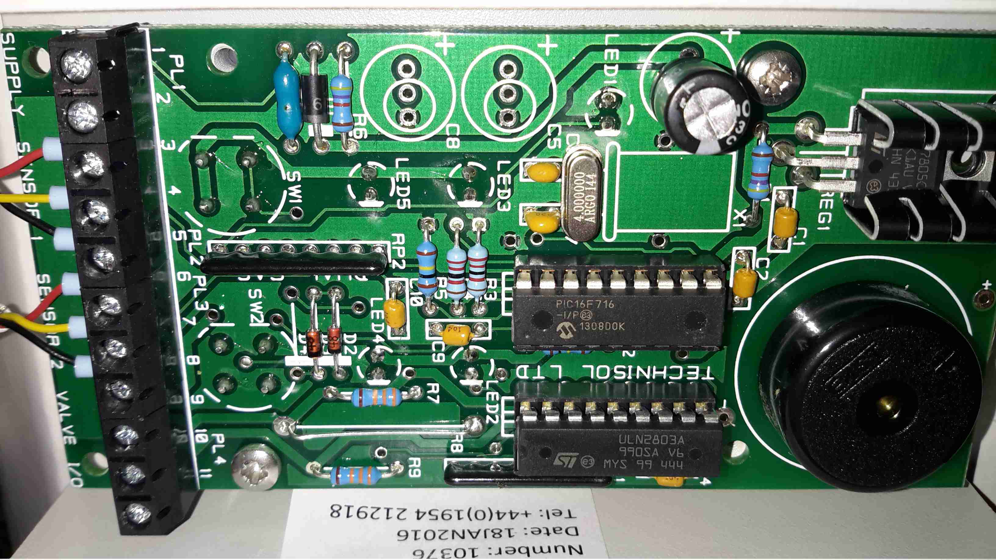
Control Board
Not much inside in the way of circuitry, the brains of the operation is a Microchip PIC16F716 8-bit microcontroller with an onboard A/D converter (needed to interface with the sensors), running at 4MHz. The solenoid valve is driven with a ULN2803 Darlington transistor array.
The alarm Piezo sounder can be seen to the right of the ICs, above that is a simple LM7805 linear regulator providing power to the electronics.
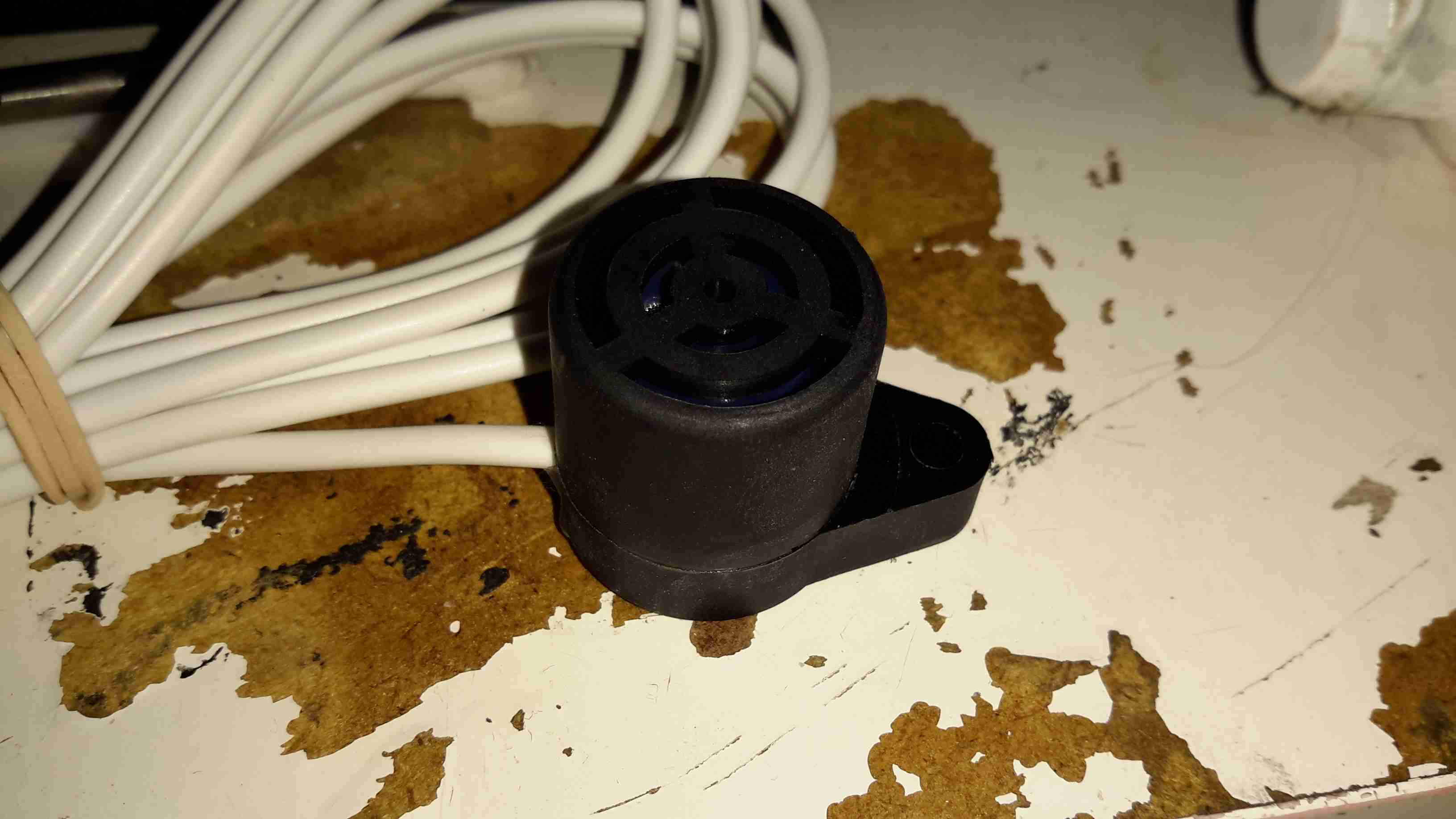
Remote Sensor
The pair of remote sensors come with 3.5m of cable, a good thing since the mounting points for these are going to be rather far from the main unit in our installation.
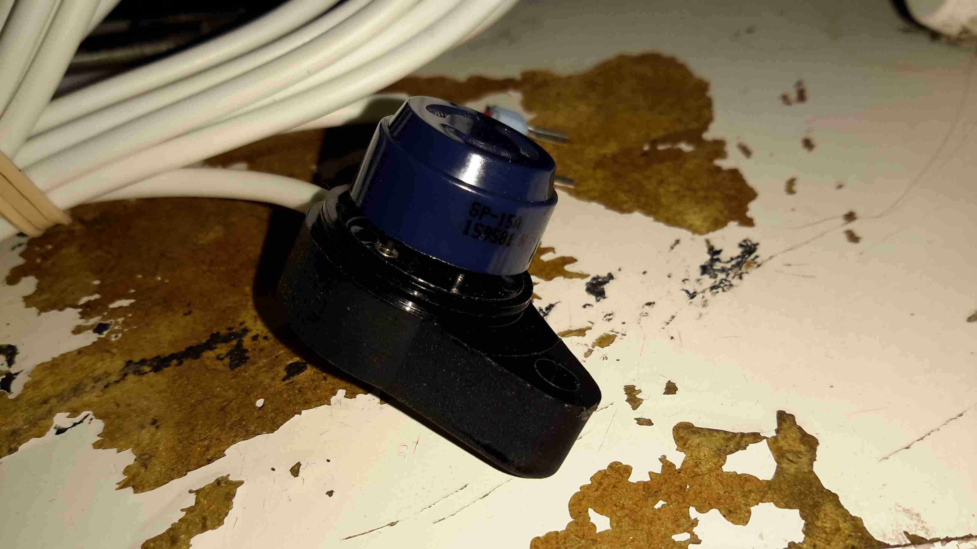
Sensor Element
The sensor itself is a SP-15A Tin Oxide semiconductor type, most sensitive to butane & propane. Unlike the Chinese El-Cheapo versions on eBay, these are high quality sensors. After whiffing some gas from a lighter at one of the sensors, the alarm triggered instantly & tripped the solenoid off.
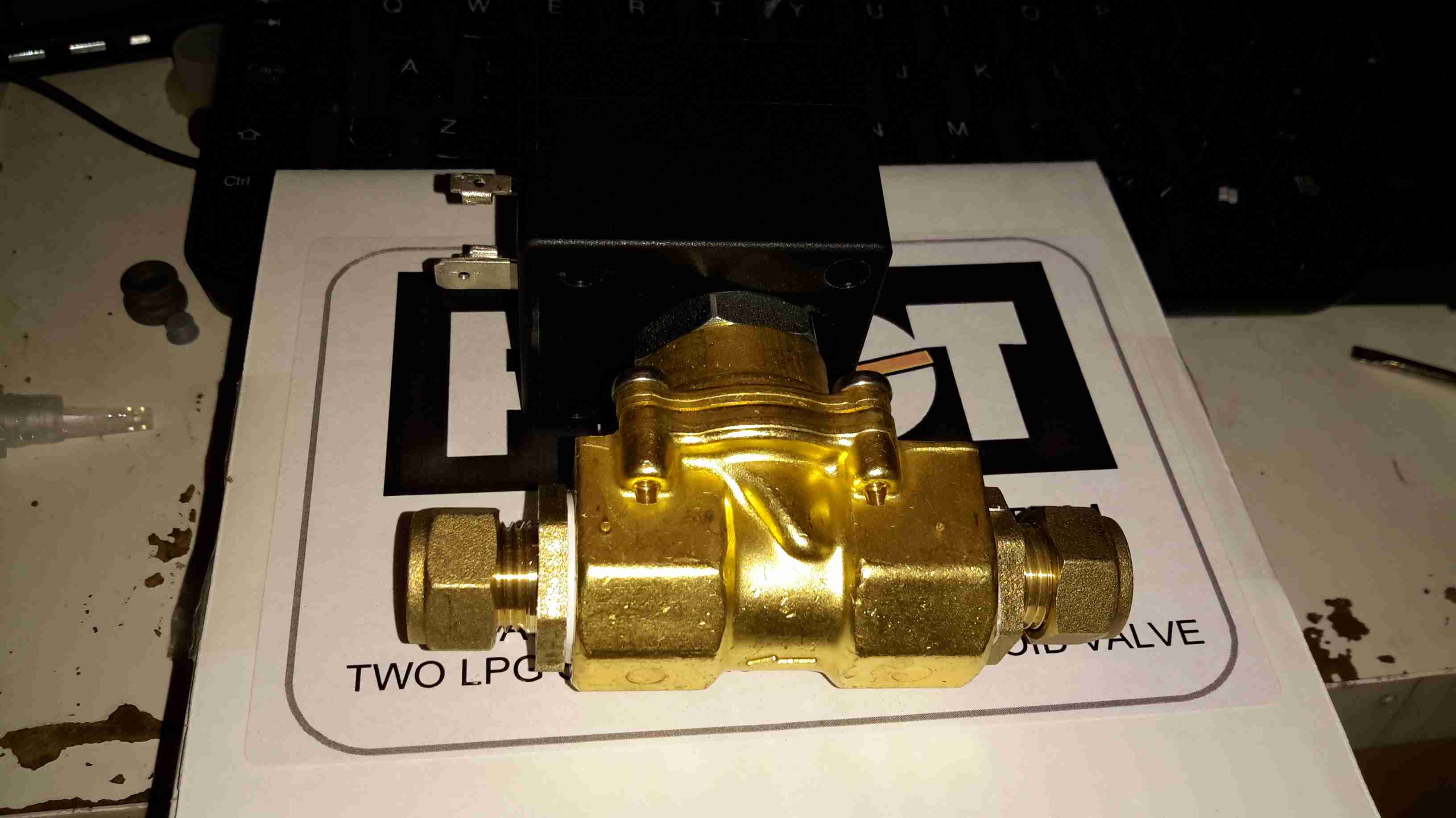
Solenoid Valve
The solenoid valve goes into the gas supply line after the bottle regulator, in this case I’ve already fitted the adaptors to take the 10mm gas line to the 1/2″ BSP threads on the valve itself. This brass lump is a bit heavy, so support will be needed to prevent vibration compromising the gas line.
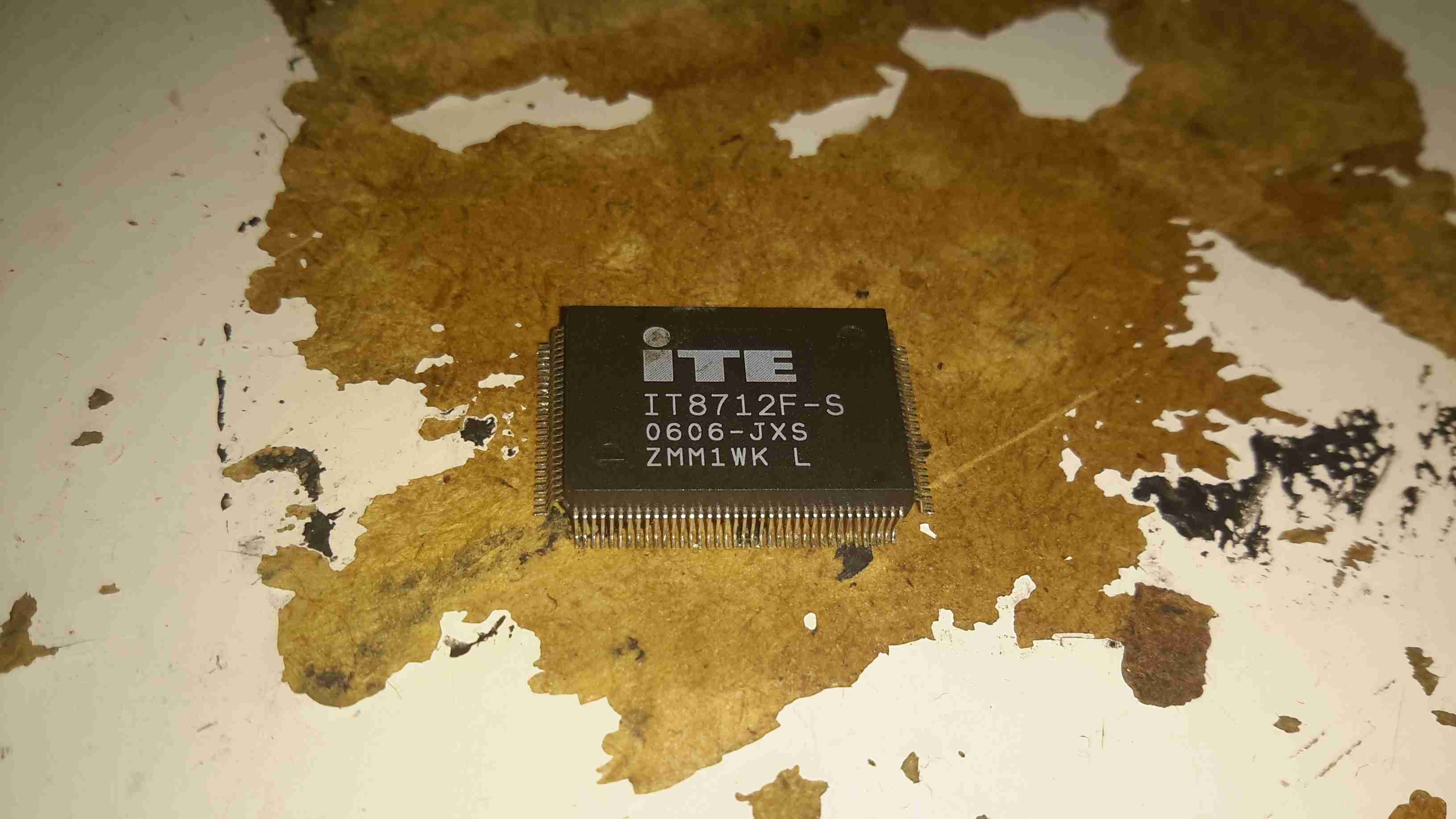
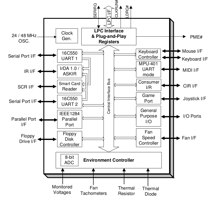
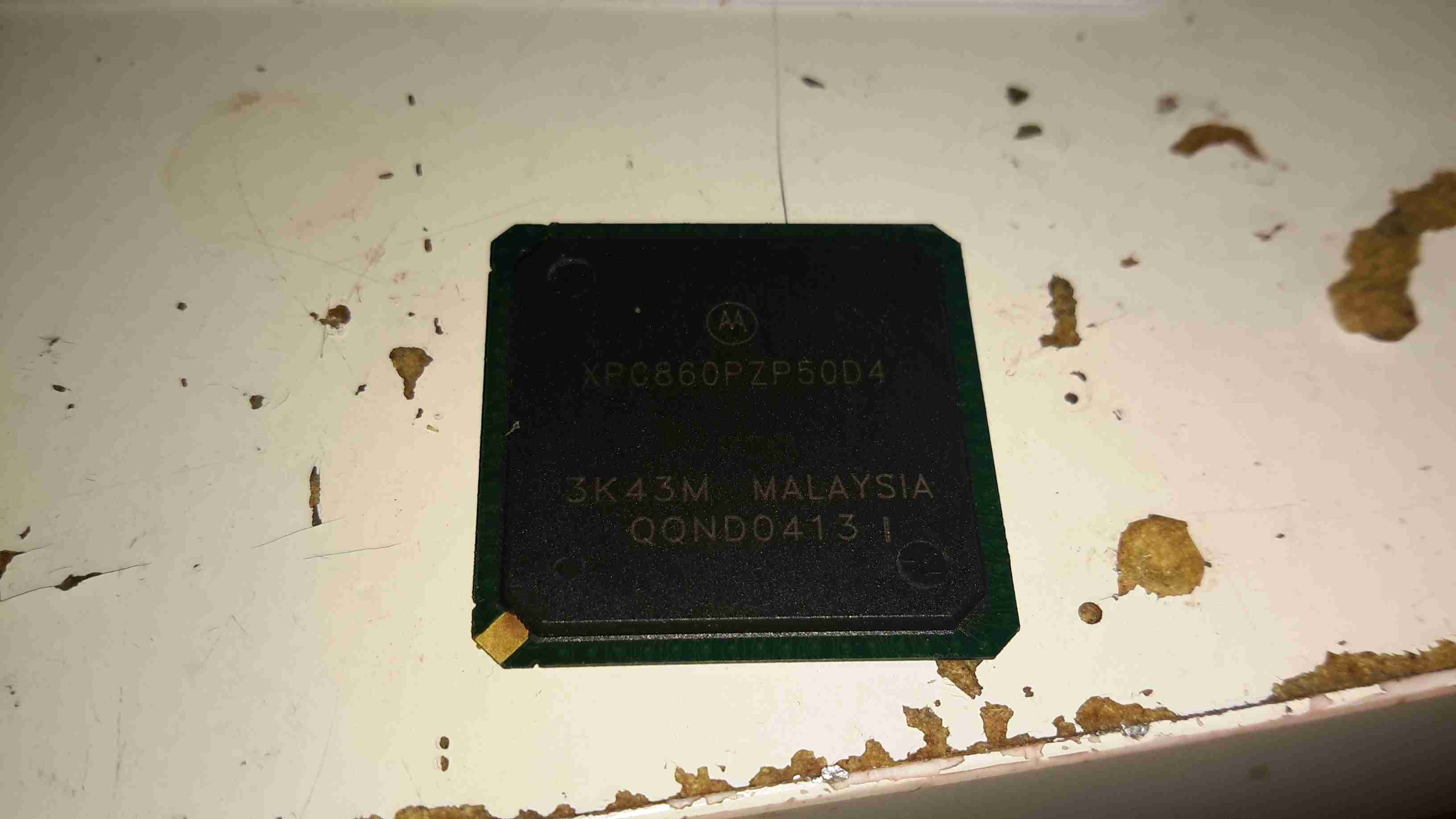
This is a System On Chip from Motorola, designed for network routing applications. This chip contains a hell of a feature set, so I’ll just include an excerpt from the datasheet:
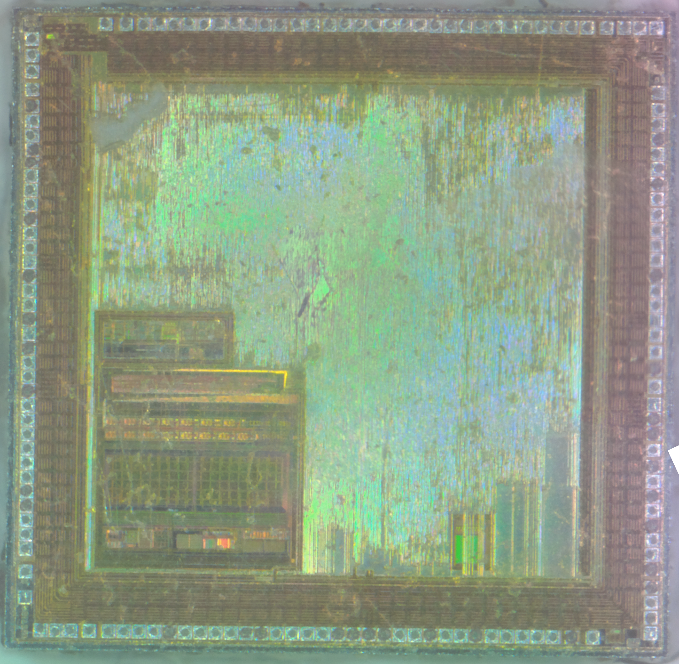
XPC860PZP50D4 Die
Embedded single-issue, 32-bit MPC8xx core (implementing the PowerPC
architecture) with thirty-two 32-bit general-purpose registers (GPRs)
— The core performs branch prediction with conditional prefetch, without
conditional execution
— 4- or 8-Kbyte data cache and 4- or 16-Kbyte instruction cache (see Table 1)
– 16-Kbyte instruction caches are four-way, set-associative with 256 sets;
4-Kbyte instruction caches are two-way, set-associative with 128 sets.
– 8-Kbyte data caches are two-way, set-associative with 256 sets; 4-Kbyte data
caches are two-way, set-associative with 128 sets.
– Cache coherency for both instruction and data caches is maintained on 128-bit
(4-word) cache blocks.
– Caches are physically addressed, implement a least recently used (LRU)
replacement algorithm, and are lockable on a cache block basis.
— Instruction and data caches are two-way, set-associative, physically addressed,
LRU replacement, and lockable on-line granularity.
— MMUs with 32-entry TLB, fully associative instruction, and data TLBs
— MMUs support multiple page sizes of 4, 16, and 512 Kbytes, and 8 Mbytes; 16
virtual address spaces and 16 protection groups
— Advanced on-chip-emulation debug mode
Up to 32-bit data bus (dynamic bus sizing for 8, 16, and 32 bits)
32 address lines
Operates at up to 80 MHz
Memory controller (eight banks)
— Contains complete dynamic RAM (DRAM) controller
— Each bank can be a chip select or RAS to support a DRAM bank
— Up to 15 wait states programmable per memory bank
— Glueless interface to DRAM, SIMMS, SRAM, EPROM, Flash EPROM, and
other memory devices.
— DRAM controller programmable to support most size and speed memory
interfaces
— Four CAS lines, four WE lines, one OE line
— Boot chip-select available at reset (options for 8-, 16-, or 32-bit memory)
— Variable block sizes (32 Kbyte to 256 Mbyte)
— Selectable write protection
— On-chip bus arbitration logic
General-purpose timers
— Four 16-bit timers or two 32-bit timers
— Gate mode can enable/disable counting
— Interrupt can be masked on reference match and event capture
System integration unit (SIU)
— Bus monitor
— Software watchdog
— Periodic interrupt timer (PIT)
— Low-power stop mode
— Clock synthesizer
— Decrementer, time base, and real-time clock (RTC) from the PowerPC
architecture
— Reset controller
— IEEE 1149.1 test access port (JTAG)
Interrupts
— Seven external interrupt request (IRQ) lines
— 12 port pins with interrupt capability
— 23 internal interrupt sources
— Programmable priority between SCCs
— Programmable highest priority request
10/100 Mbps Ethernet support, fully compliant with the IEEE 802.3u Standard (not
available when using ATM over UTOPIA interface)
ATM support compliant with ATM forum UNI 4.0 specification
— Cell processing up to 50–70 Mbps at 50-MHz system clock
— Cell multiplexing/demultiplexing
— Support of AAL5 and AAL0 protocols on a per-VC basis. AAL0 support enables
OAM and software implementation of other protocols).
— ATM pace control (APC) scheduler, providing direct support for constant bit rate
(CBR) and unspecified bit rate (UBR) and providing control mechanisms
enabling software support of available bit rate (ABR)
— Physical interface support for UTOPIA (10/100-Mbps is not supported with this
interface) and byte-aligned serial (for example, T1/E1/ADSL)
— UTOPIA-mode ATM supports level-1 master with cell-level handshake,
multi-PHY (up to 4 physical layer devices), connection to 25-, 51-, or 155-Mbps
framers, and UTOPIA/system clock ratios of 1/2 or 1/3.
— Serial-mode ATM connection supports transmission convergence (TC) function
for T1/E1/ADSL lines; cell delineation; cell payload scrambling/descrambling;
automatic idle/unassigned cell insertion/stripping; header error control (HEC)
generation, checking, and statistics.
Communications processor module (CPM)
— RISC communications processor (CP)
— Communication-specific commands (for example, GRACEFUL STOP TRANSMIT ,
ENTER HUNT MODE , and RESTART TRANSMIT )
— Supports continuous mode transmission and reception on all serial channels
— Up to 8Kbytes of dual-port RAM
— 16 serial DMA (SDMA) channels
— Three parallel I/O registers with open-drain capability
Four baud-rate generators (BRGs)
— Independent (can be connected to any SCC or SMC)
— Allow changes during operation
— Autobaud support option
Four serial communications controllers (SCCs)
— Ethernet/IEEE 802.3 optional on SCC1–4, supporting full 10-Mbps operation
(available only on specially programmed devices).
— HDLC/SDLC (all channels supported at 2 Mbps)
— HDLC bus (implements an HDLC-based local area network (LAN))
— Asynchronous HDLC to support PPP (point-to-point protocol)
— AppleTalk
— Universal asynchronous receiver transmitter (UART)
— Synchronous UART
— Serial infrared (IrDA)
— Binary synchronous communication (BISYNC)
— Totally transparent (bit streams)
— Totally transparent (frame based with optional cyclic redundancy check (CRC))
Two SMCs (serial management channels)
— UART
— Transparent
— General circuit interface (GCI) controller
— Can be connected to the time-division multiplexed (TDM) channels
One SPI (serial peripheral interface)
— Supports master and slave modes
— Supports multimaster operation on the same bus
One I 2 C (inter-integrated circuit) port
— Supports master and slave modes
— Multiple-master environment support
Time-slot assigner (TSA)
— Allows SCCs and SMCs to run in multiplexed and/or non-multiplexed operation
— Supports T1, CEPT, PCM highway, ISDN basic rate, ISDN primary rate, user
defined
— 1- or 8-bit resolution
— Allows independent transmit and receive routing, frame synchronization,
clocking
— Allows dynamic changes
— Can be internally connected to six serial channels (four SCCs and two SMCs)
Parallel interface port (PIP)
— Centronics interface support
— Supports fast connection between compatible ports on the MPC860 or the
MC68360
PCMCIA interface
— Master (socket) interface, release 2.1 compliant
— Supports two independent PCMCIA sockets
— Eight memory or I/O windows supported
Low power support
— Full on—all units fully powered
— Doze—core functional units disabled, except time base decrementer, PLL,
memory controller, RTC, and CPM in low-power standby
— Sleep—all units disabled, except RTC and PIT, PLL active for fast wake up
— Deep sleep—all units disabled including PLL, except RTC and PIT
— Power down mode— all units powered down, except PLL, RTC, PIT, time base,
and decrementer
Debug interface
— Eight comparators: four operate on instruction address, two operate on data
address, and two operate on data
— Supports conditions: = ≠ < >
— Each watchpoint can generate a break-point internally
3.3 V operation with 5-V TTL compatibility except EXTAL and EXTCLK
357-pin ball grid array (BGA) package
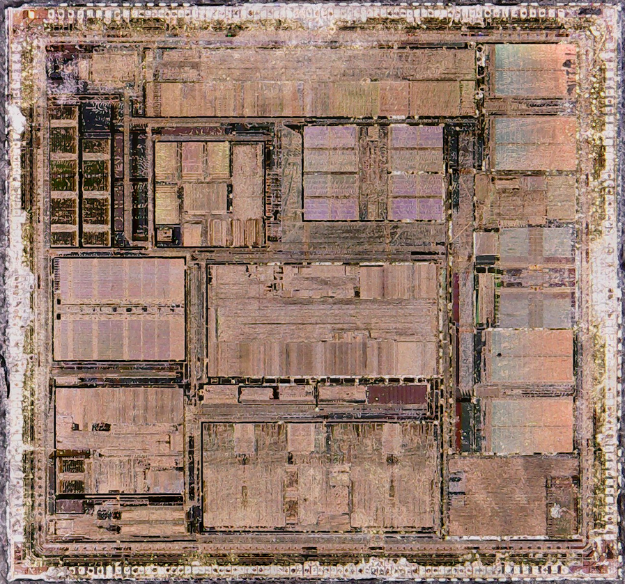
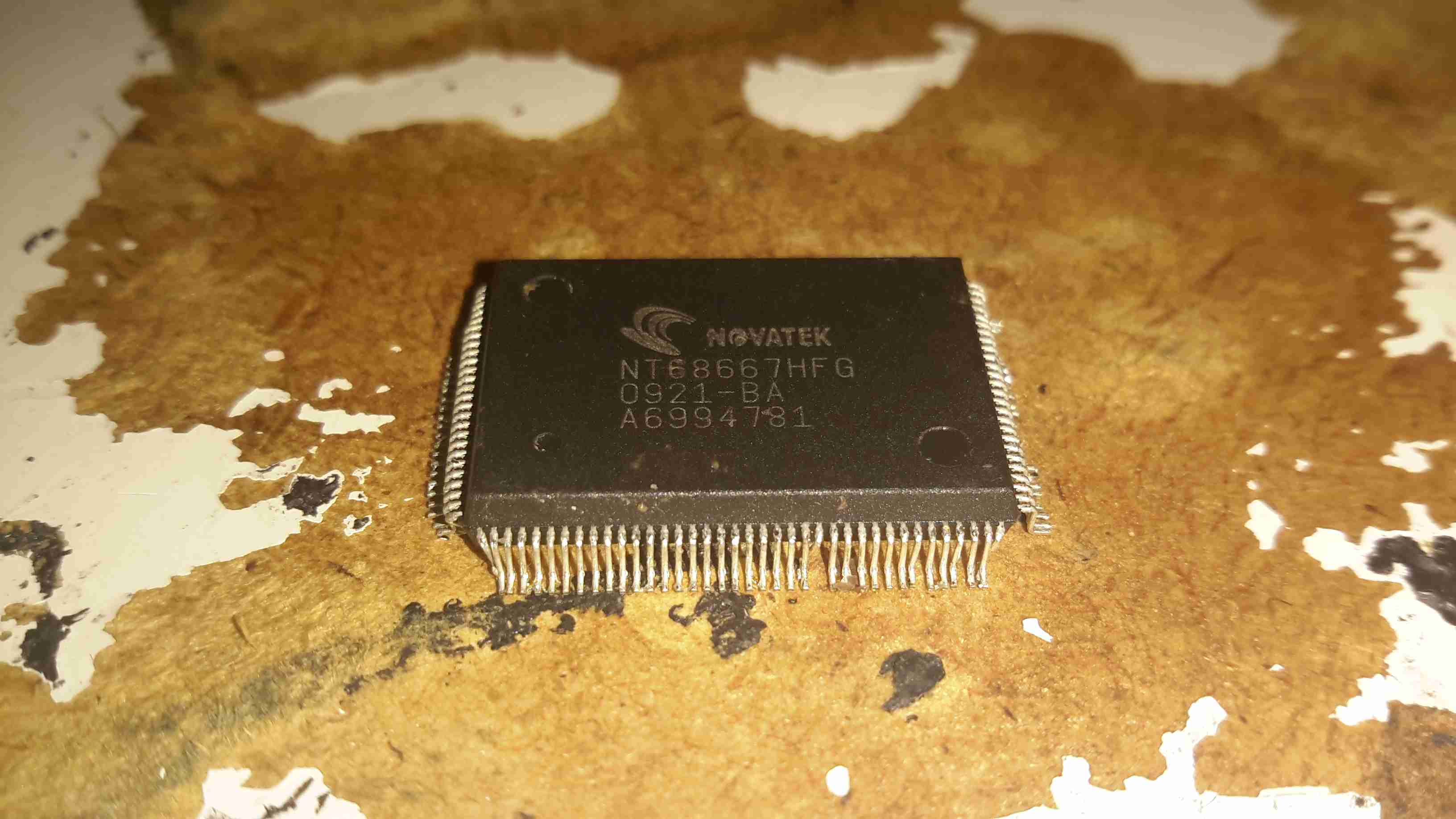
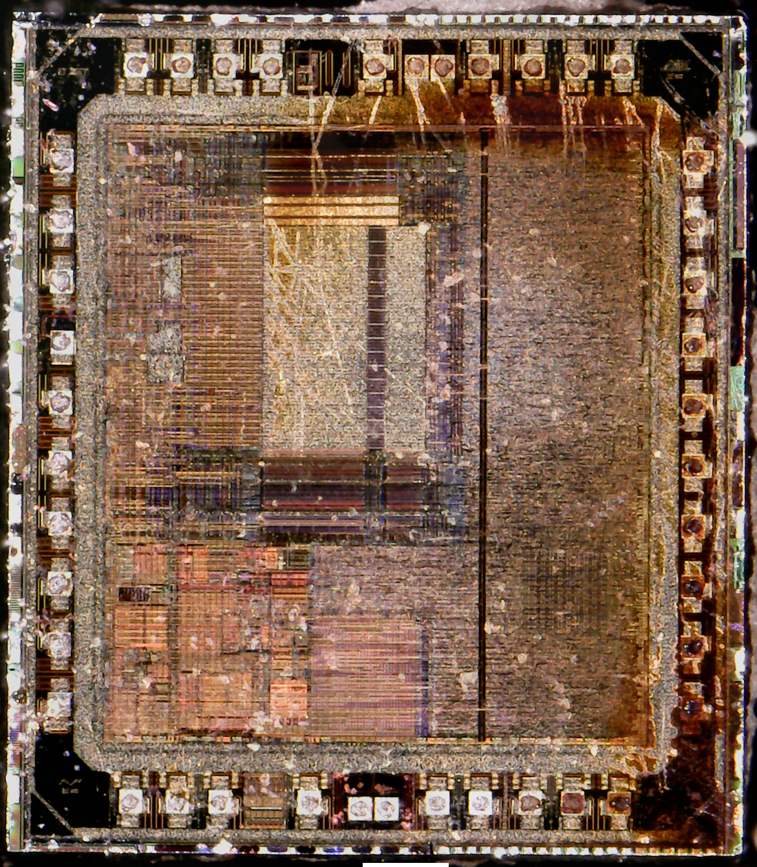
This is an Audio DSP chip from the early 90’s, used for sound effects in audio mixing consoles. Unfortunately I couldn’t find much info on these.
TMS57002 Die
The die is massive, 10mm square at least. Interestingly, the markings on the die indicate it’s a TMS67002, maybe there was a different internal software version for the 57002 with fewer features, that used the same Silicon? In the centre of this die, there’s an area that looks like mask ROM, with the individual memory bits visible.
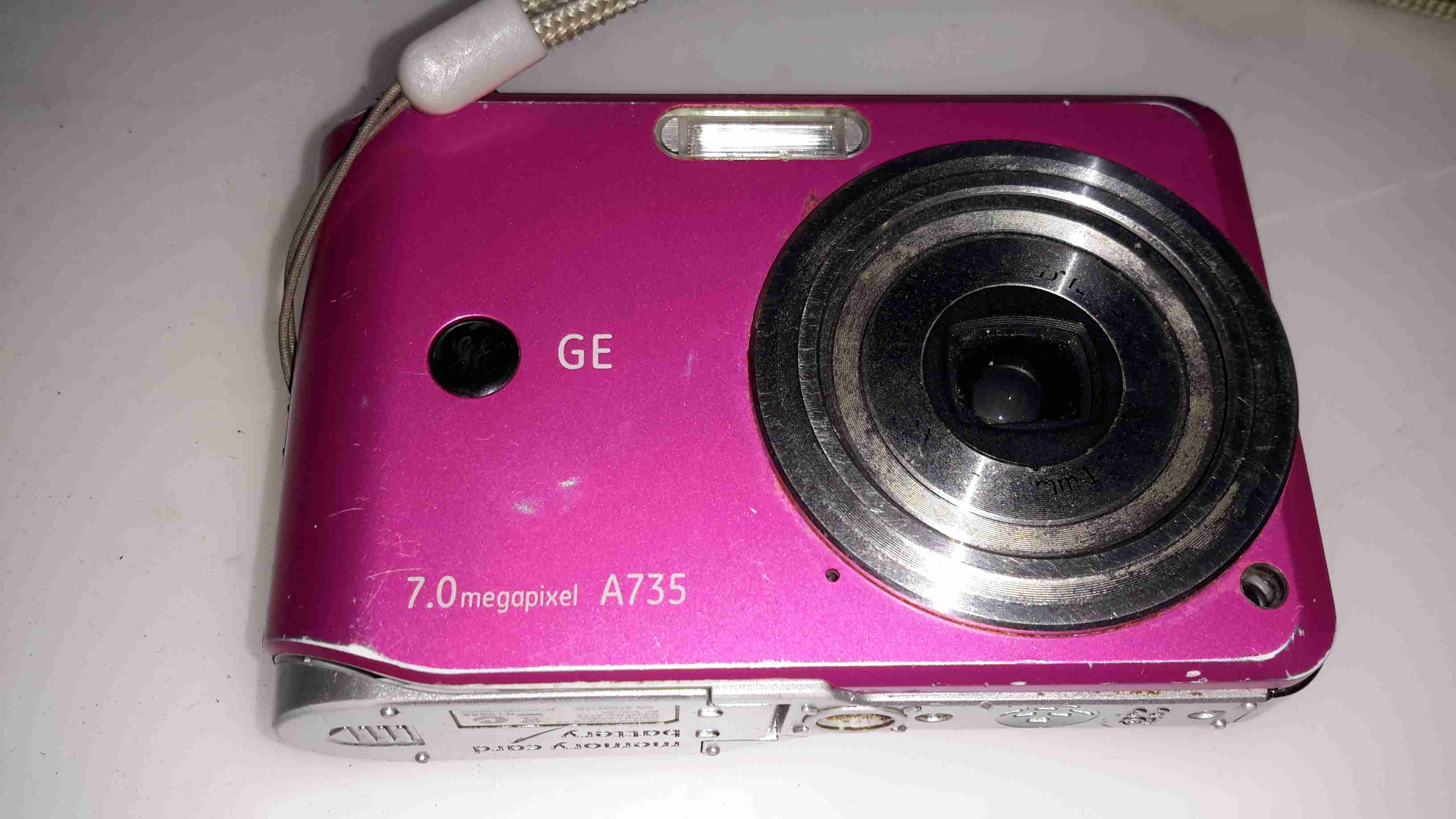
This camera has now been retired after many years of heavy use. Exposure to a 3-year old has caused severe damage to the lens mechanism, which no longer functions correctly.
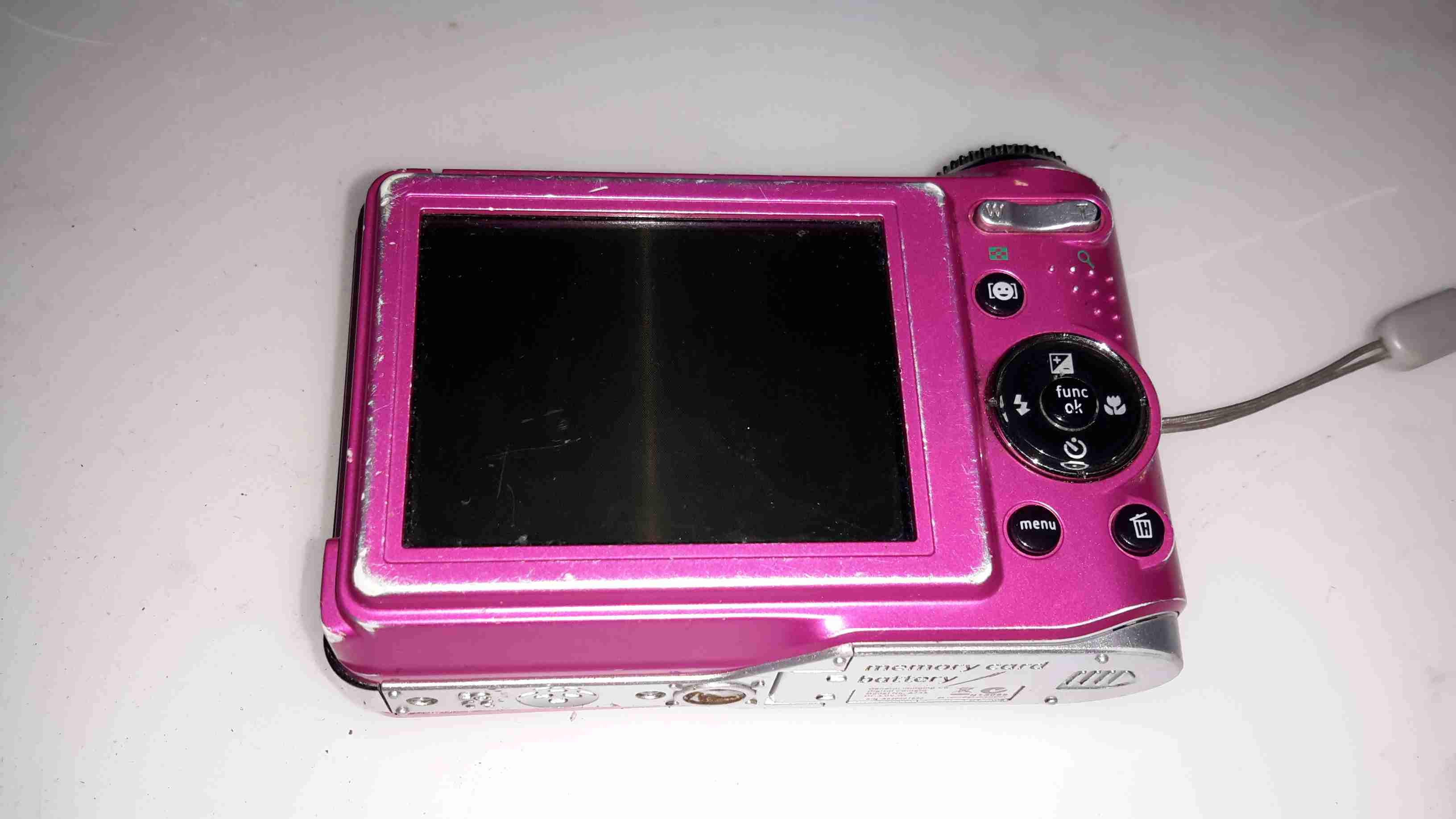
Rear Panel
Pretty much standard interface for a digital camera, with a nice large LCD for it’s time.
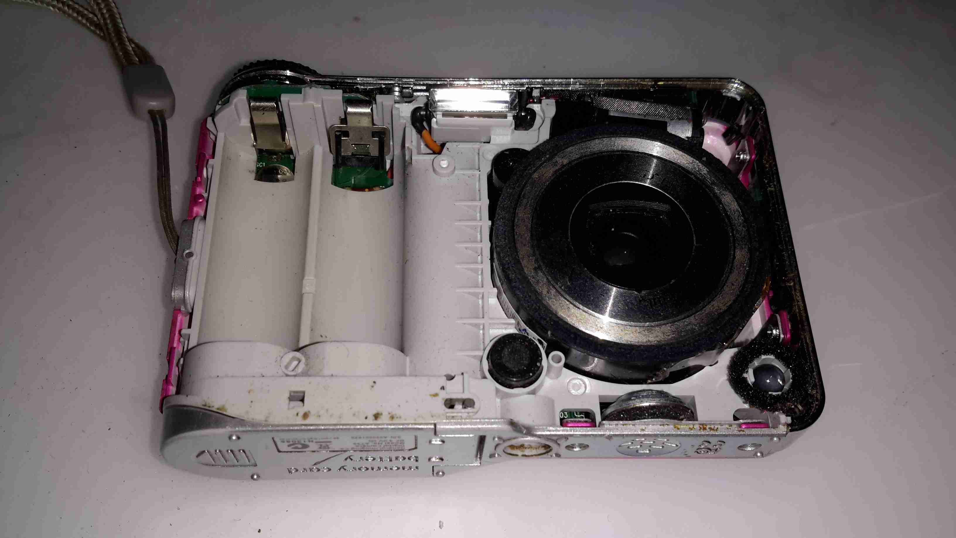
Front Cover Removed
With the front cover removed, the lens assembly & battery compartment is exposed.
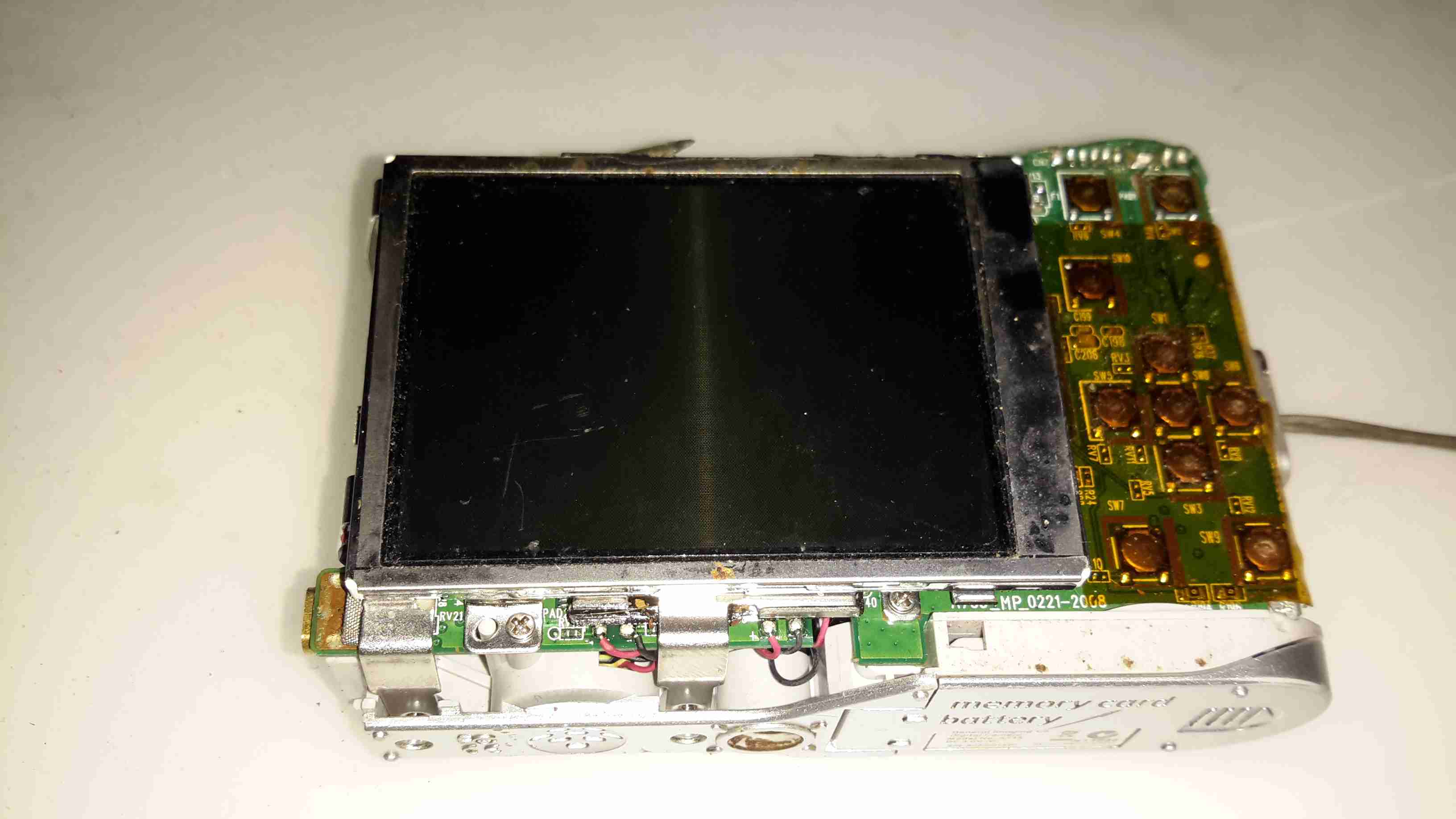
Rear Cover Removed
Removing the rear cover exposes the LCD module & the main PCB, the interface tactile switches are on the right under a protective layer of Kapton tape.
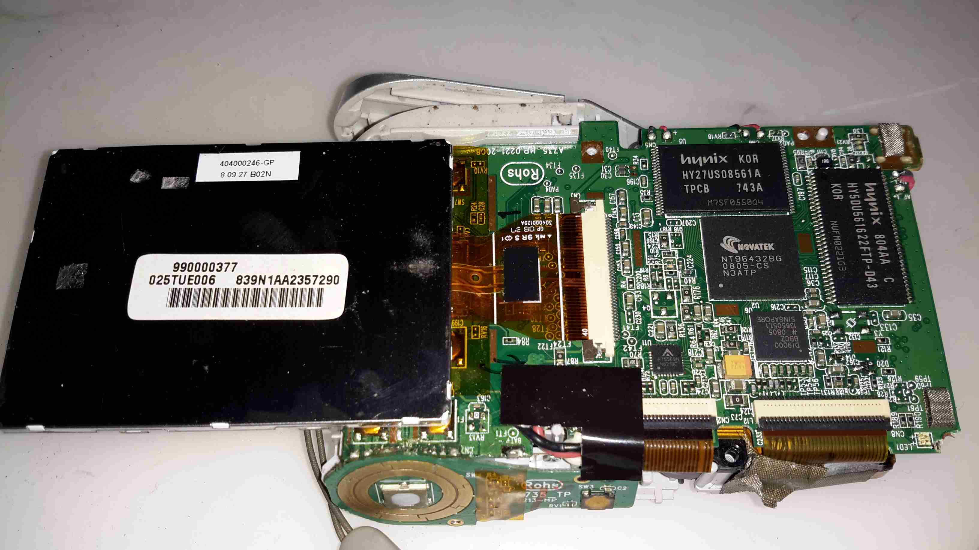
Main Chipset
Flipping the LCD out of it’s mounting bracket reveals the main camera chipset. The CPU is a NovaTek NT96432BG, no doubt a SoC of some kind, but I couldn’t find any information. Firmware & inbuilt storage is on a Hynix HY27US08561A 256MBit NAND Flash, with a Hynix HY5DU561622FTP-D43 256Mbit DRAM for system memory.
I couldn’t find any info on the other two chips on this side of the board, but one is probably a motor driver for the lens, while the other must be the front end for the CCD sensor input to the SoC.
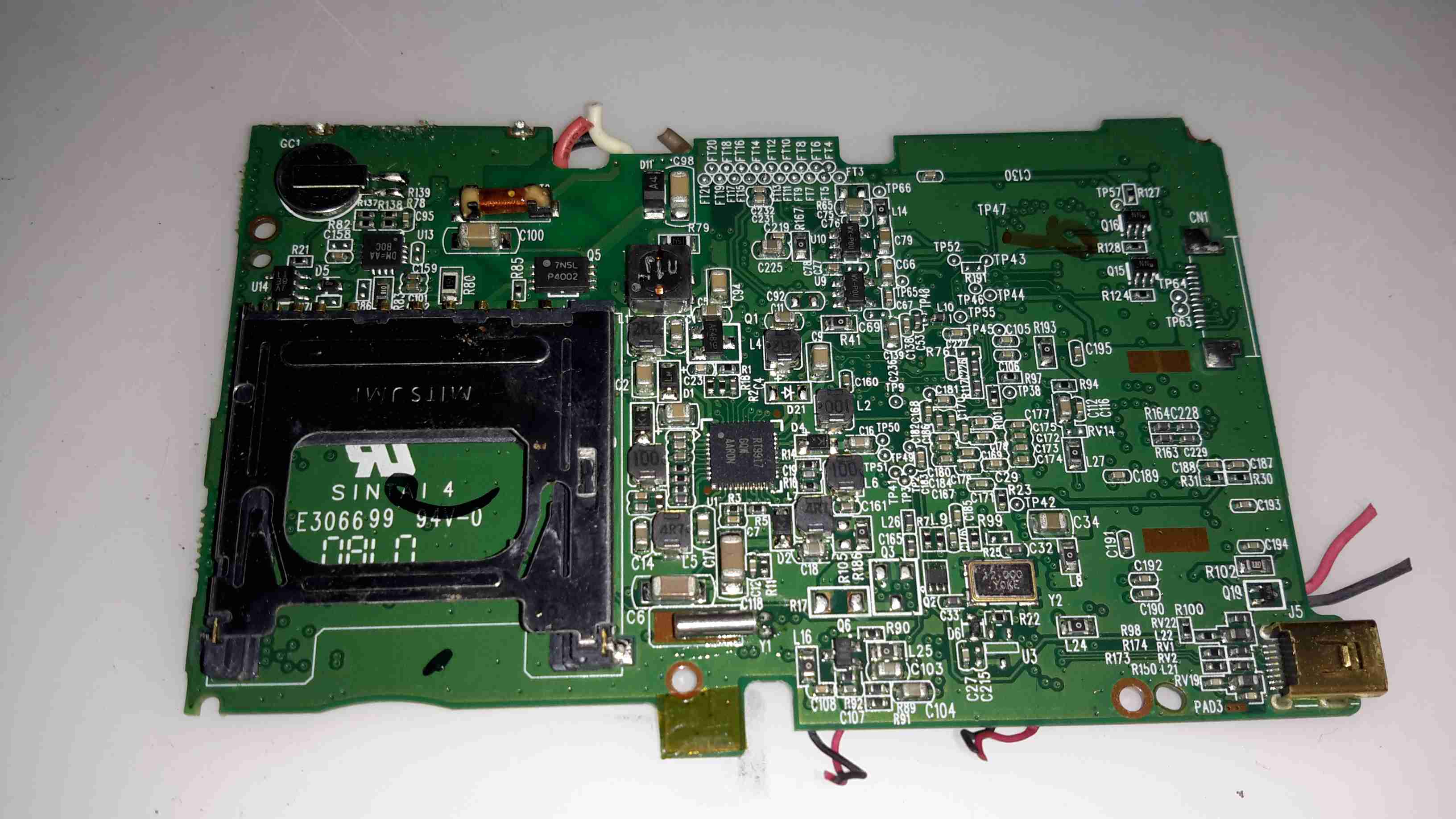
Main PCB Reverse
The other side of the PCB handles the SD card slot & power management. All the required DC rails are provided for by a RT9917 7-Channel DC-DC converter from RichTek, an IC designed specifically for digital camera applications.
Top left above the SD card slot is the trigger circuitry for the Xenon flash tube & the RTC backup battery.
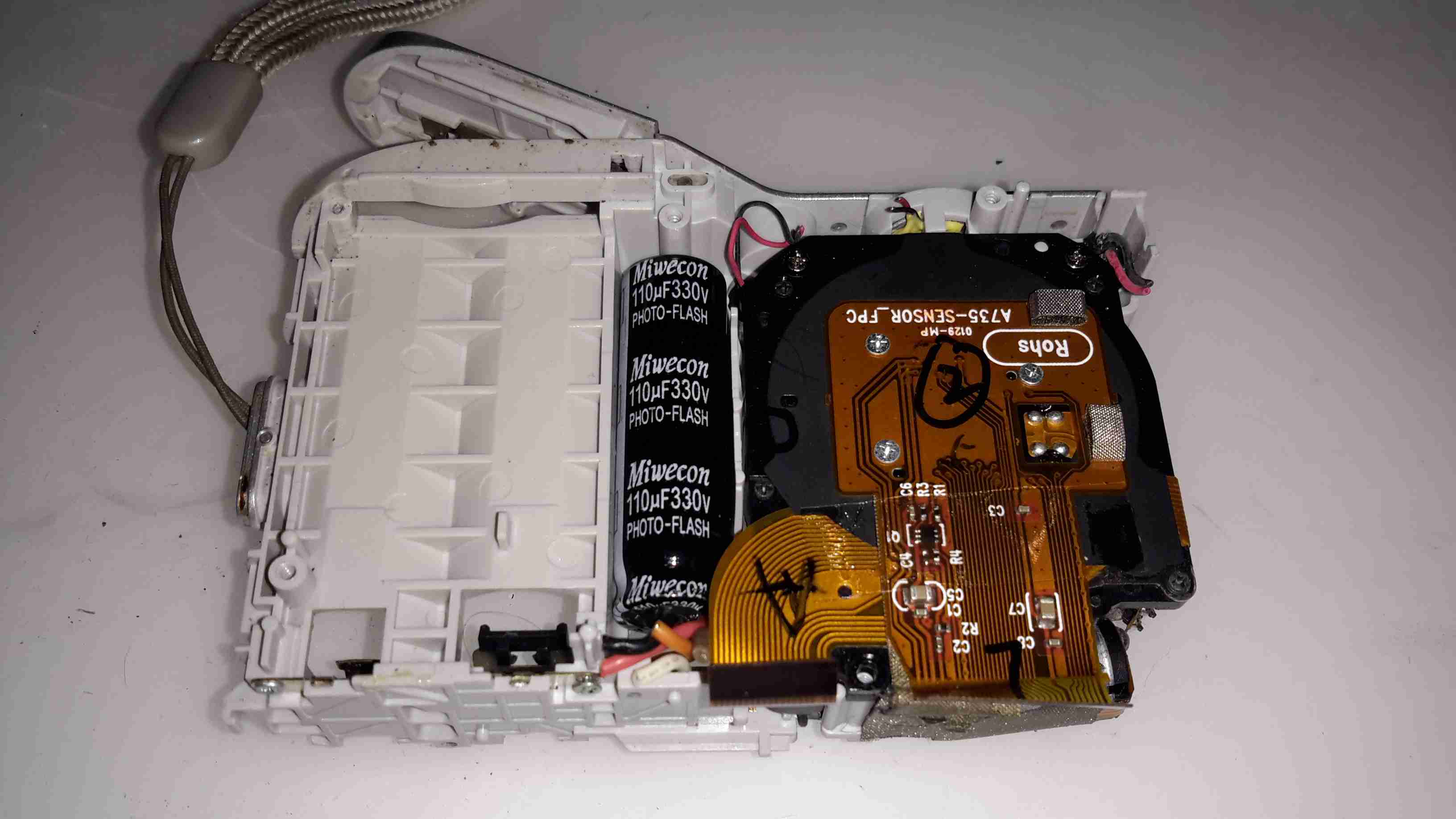
Main PCB Removed
Once the main PCB is out of the frame, the back of the lens module with the CCD is accessible. Just to the left is the high-voltage photoflash capacitor, 110µF 330v. These can give quite the kick when charged! Luckily this camera has been off long enough for the charge to bleed off.
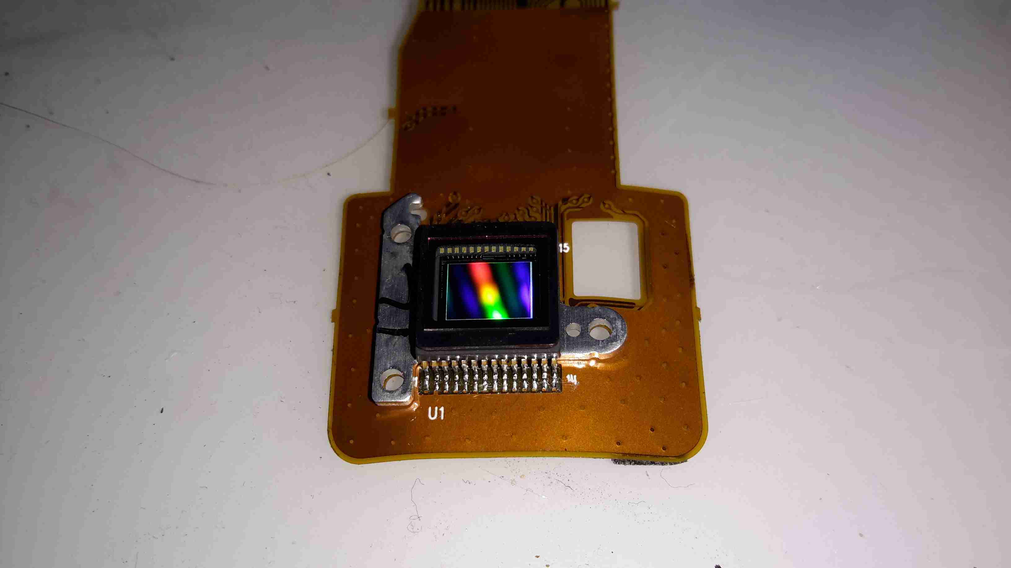
Sensor
Finally, here’s the 7-Megapixel CCD sensor removed from the lens assembly, with it’s built in IR cut filter over the top. I couldn’t find any make or model numbers on this part, as the Aluminium mounting bracket behind is bonded to the back of the sensor with epoxy, blocking access to any part information.
Die images of the chipset to come once I get round to decapping them!
As I’ve been posting some photos of decapped ICs lately, I thought I’d share the process I use personally for those that might want to give it a go 😉
The usual method for removing the epoxy package from the silicon is to use hot, concentrated Nitric Acid. Besides the obvious risks of having hot acids around, the decomposition products of the acid, namely NO² (Nitrogen Dioxide) & NO (Nitrogen Oxide), are toxic and corrosive. So until I can get the required fume hood together to make sure I’m not going to corrode the place away, I’ll leave this process to proper labs ;).
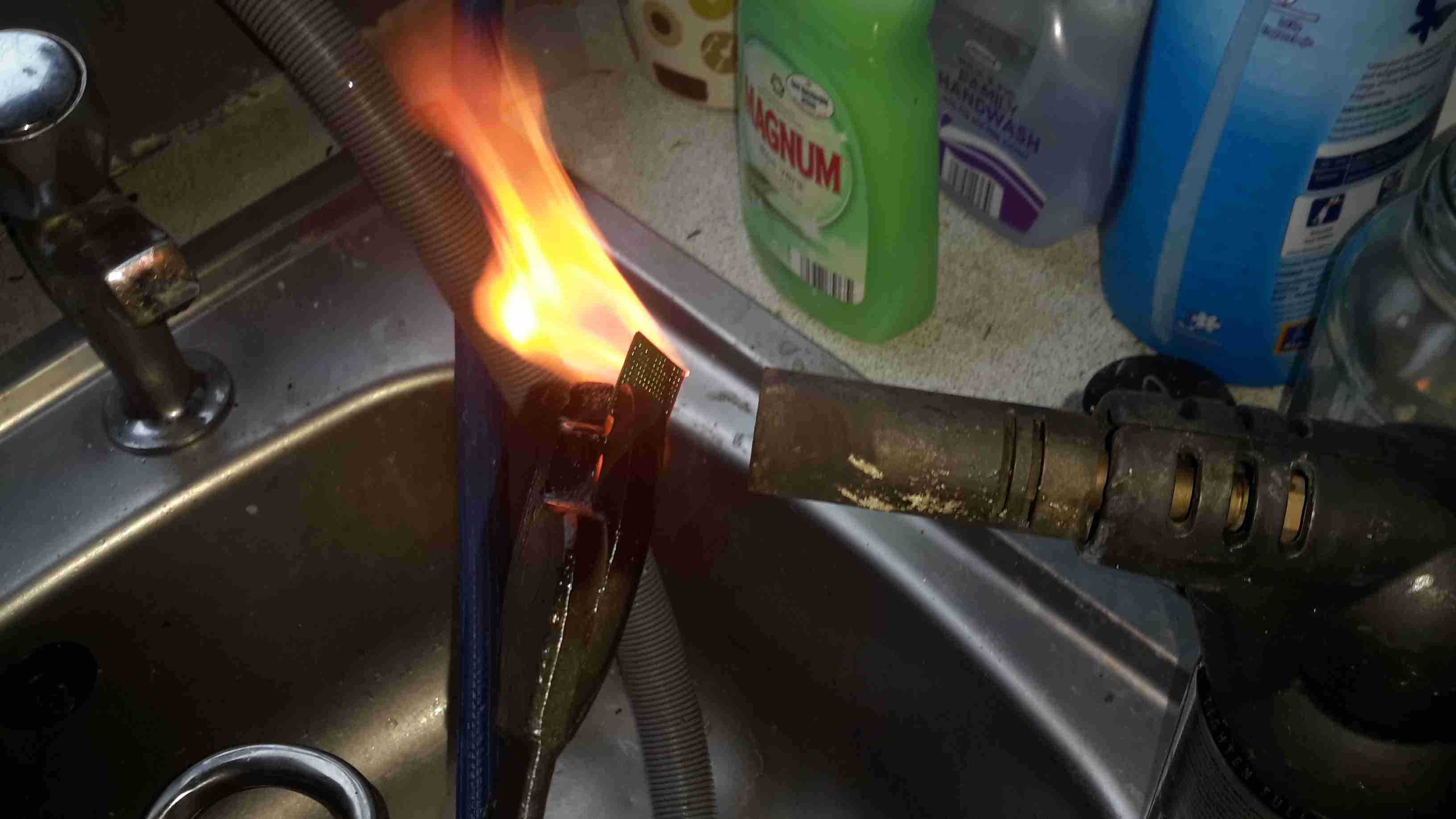
The method I use is heat based, using a Propane torch to destroy the epoxy package, without damaging the Silicon die too much.
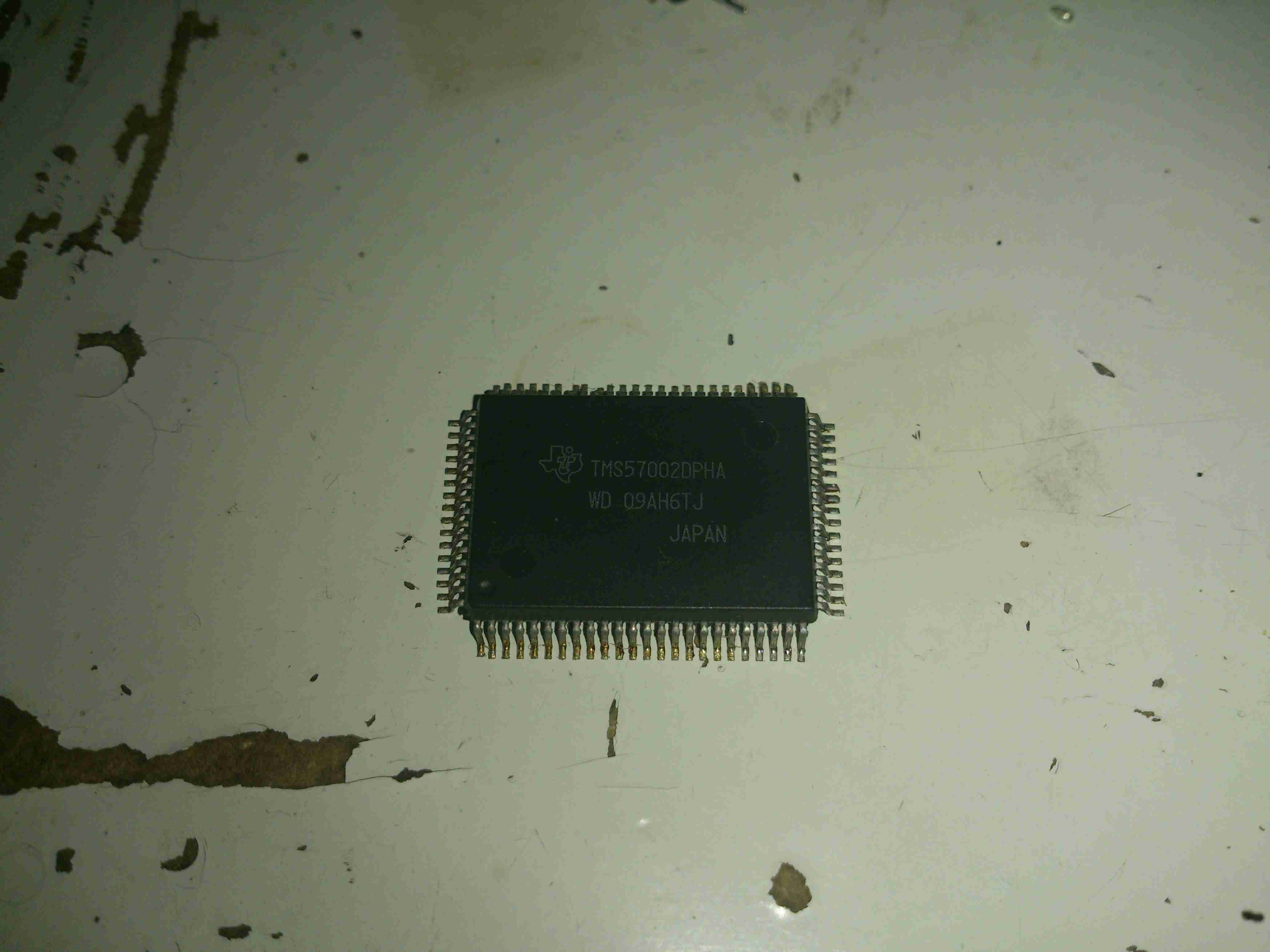
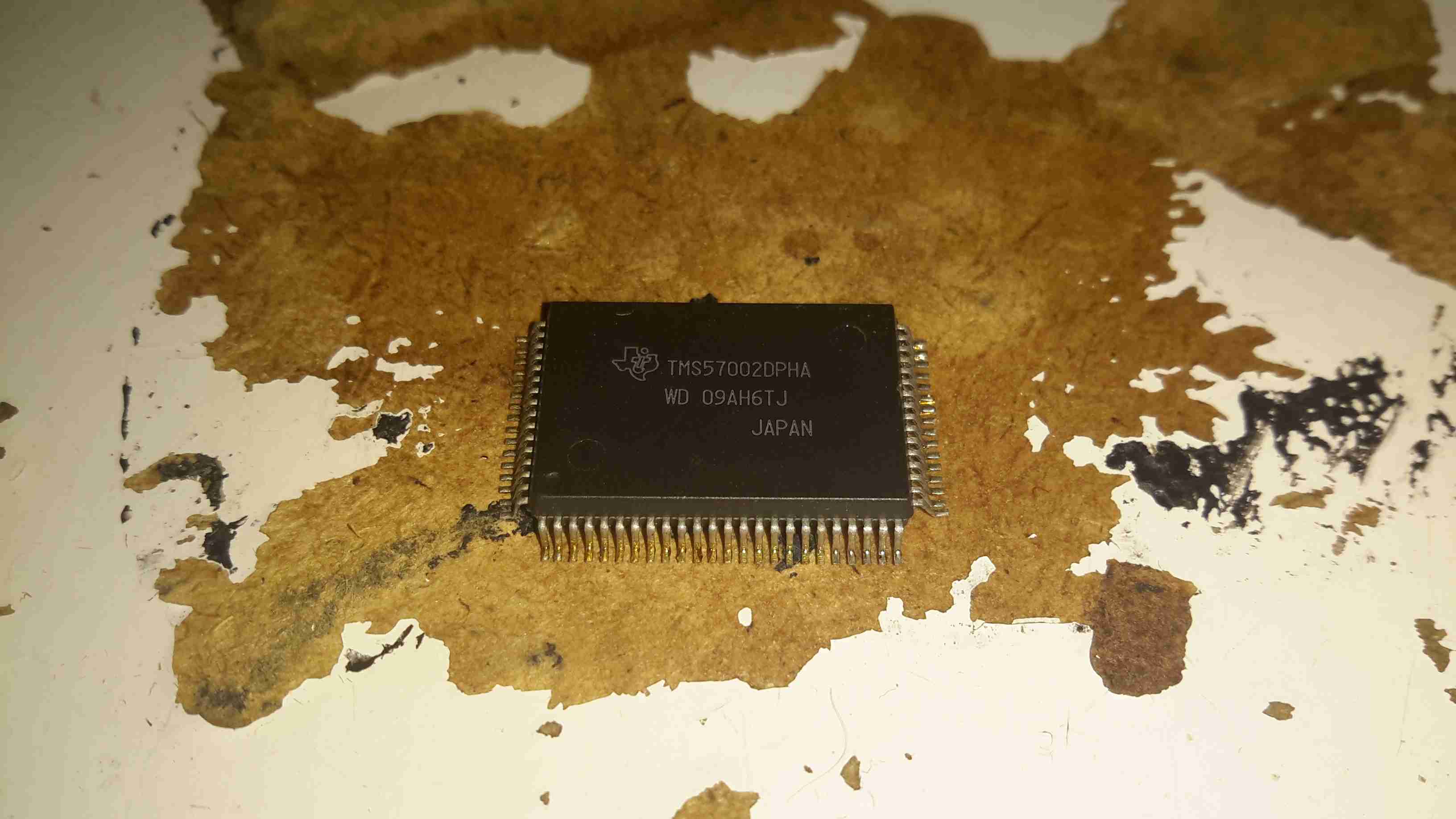
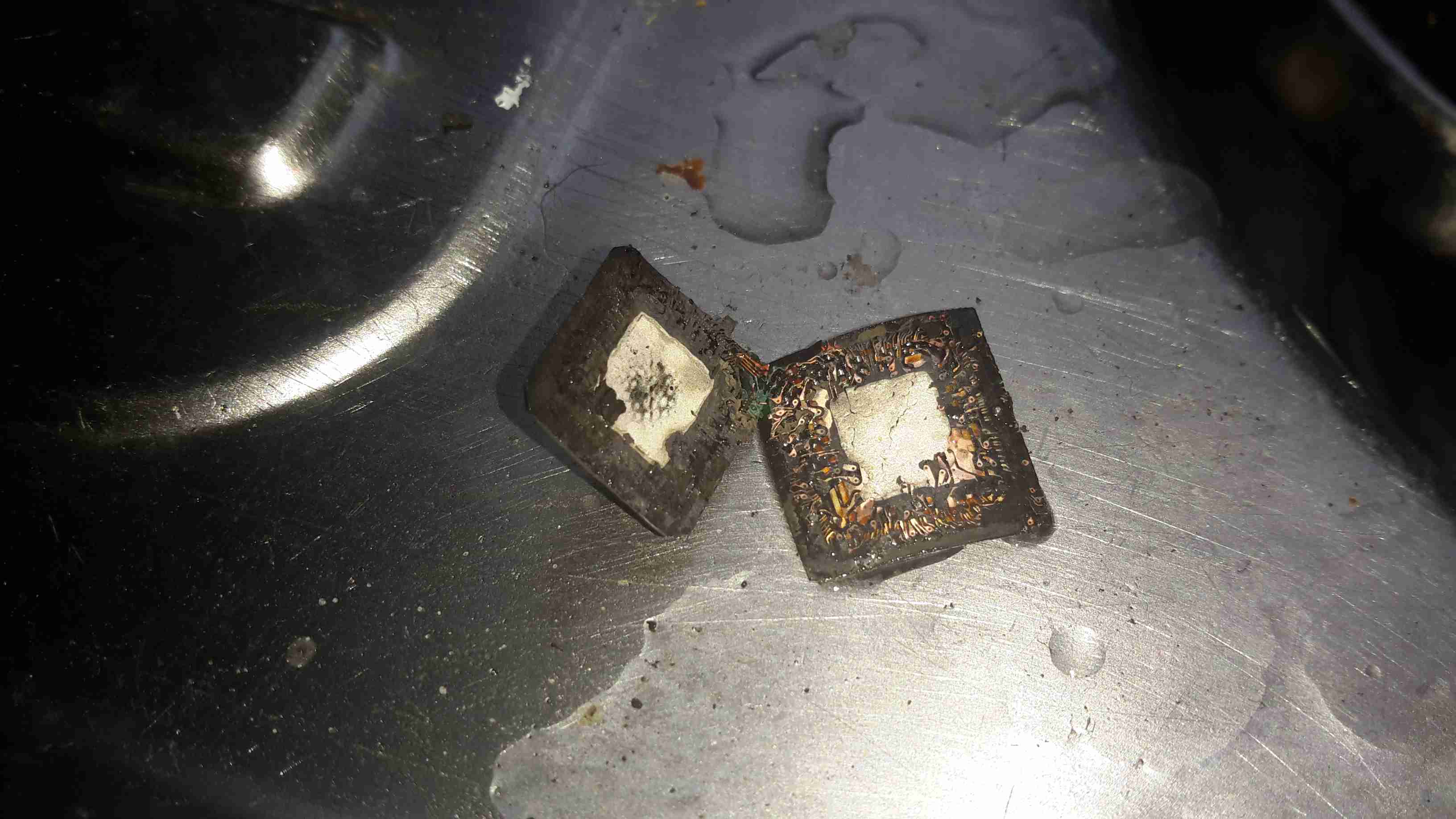
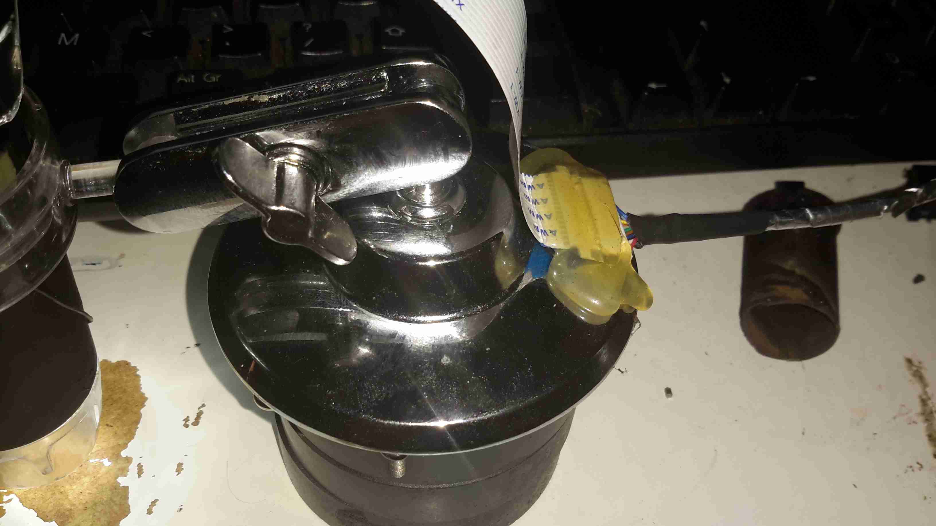
TMS57002 Audio DSP
I start off, obviously, with a desoldered IC, the one above an old audio DSP from TI. I usually desolder en-masse for this with a heat gun, stripping the entire board in one go.
FLAMES!
Next is to apply the torch to the IC. A bit of practice is required here to get the heat level & time exactly right, overheating will cause the die to oxidize & blacken or residual epoxy to stick to the surface.
I usually apply the torch until the package just about stops emitting it’s own yellow flames, meaning the epoxy is almost completely burned away. I also keep the torch flame away from the centre of the IC, where the die is located.
Breathing the fumes from this process isn’t recommended, no doubt besides the obvious soot, the burning plastic will be emitting many compounds not brilliant for Human health!
Once the IC is roasted to taste, it’s quenched in cold water for a few seconds. Sometimes this causes such a high thermal shock that the leadframe cracks off the epoxy around the die perfectly.
All Your Die Belong To Us
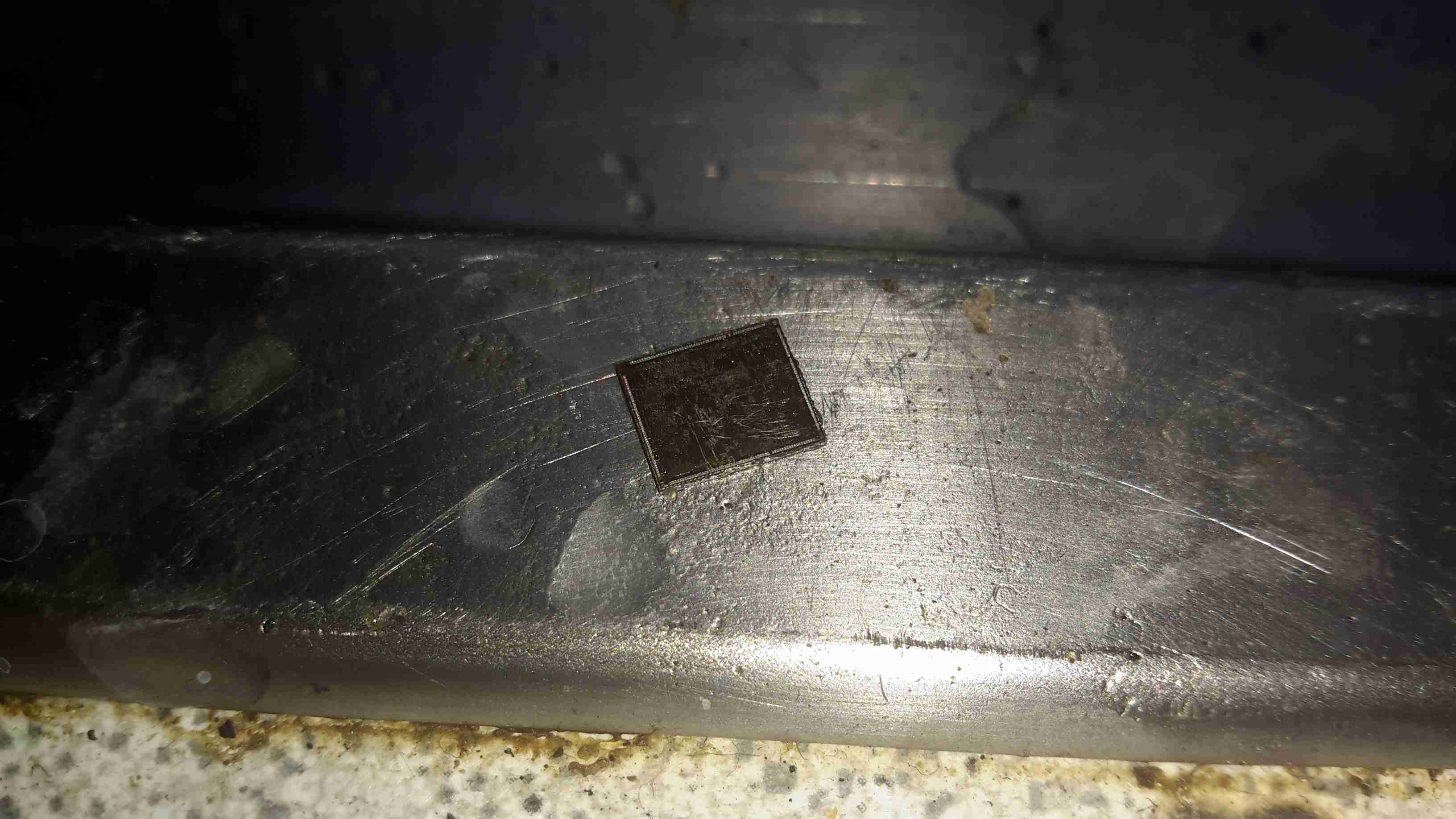
Now that the epoxy has been destroyed, it breaks apart easily, and is picked away until I uncover the die itself. (It’s the silver bit in the middle of the left half). The heat from the torch usually destroys the Silver epoxy holding the die to the leadframe, and can be removed easily from the remaining package.
Decapped
BGA packages are usually the easiest to decap, flip-chip packages are a total pain due to the solder balls being on the front side of the die, I haven’t managed to get a good result here yet, I’ll probably need to chemically remove the first layer of the die to get at the interesting bits 😉
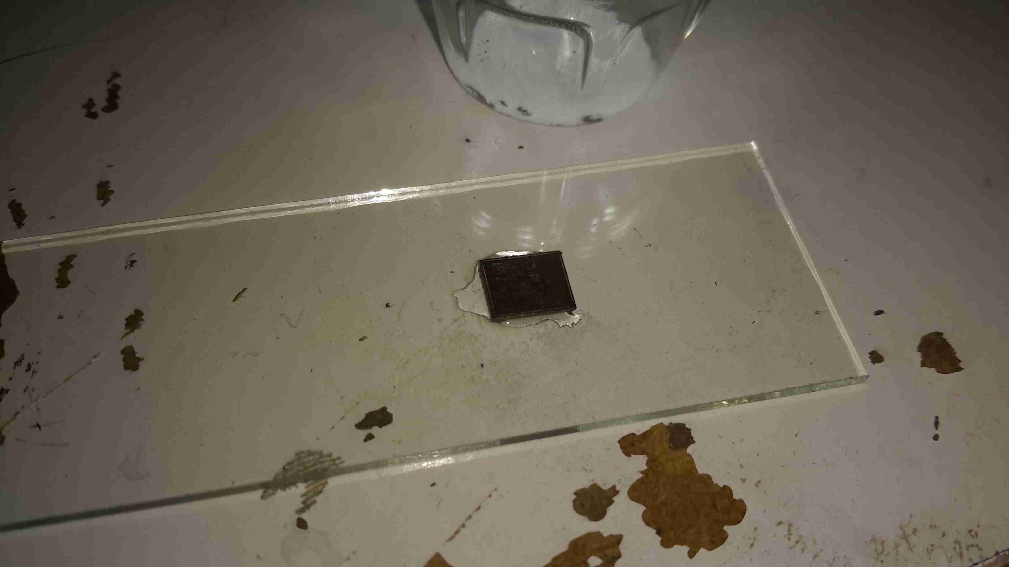
Slide
Once the die has been rinsed in clean water & inspected, it’s mounted on a glass microscope slide with a small spot of Cyanoacrylate glue to make handling easier.
Some dies require some cleaning after decapping, for this I use 99% Isopropanol & 99% Acetone, on the end of a cotton bud. Any residual epoxy flakes or oxide stuck to the die can be relatively easily removed with a fingernail – turns out fingernails are hard enough to remove the contamination, but not hard enough to damage the die features.
Once cleaning is complete, the slide is marked with the die identification, and the photographing can begin.
Microscope Mods
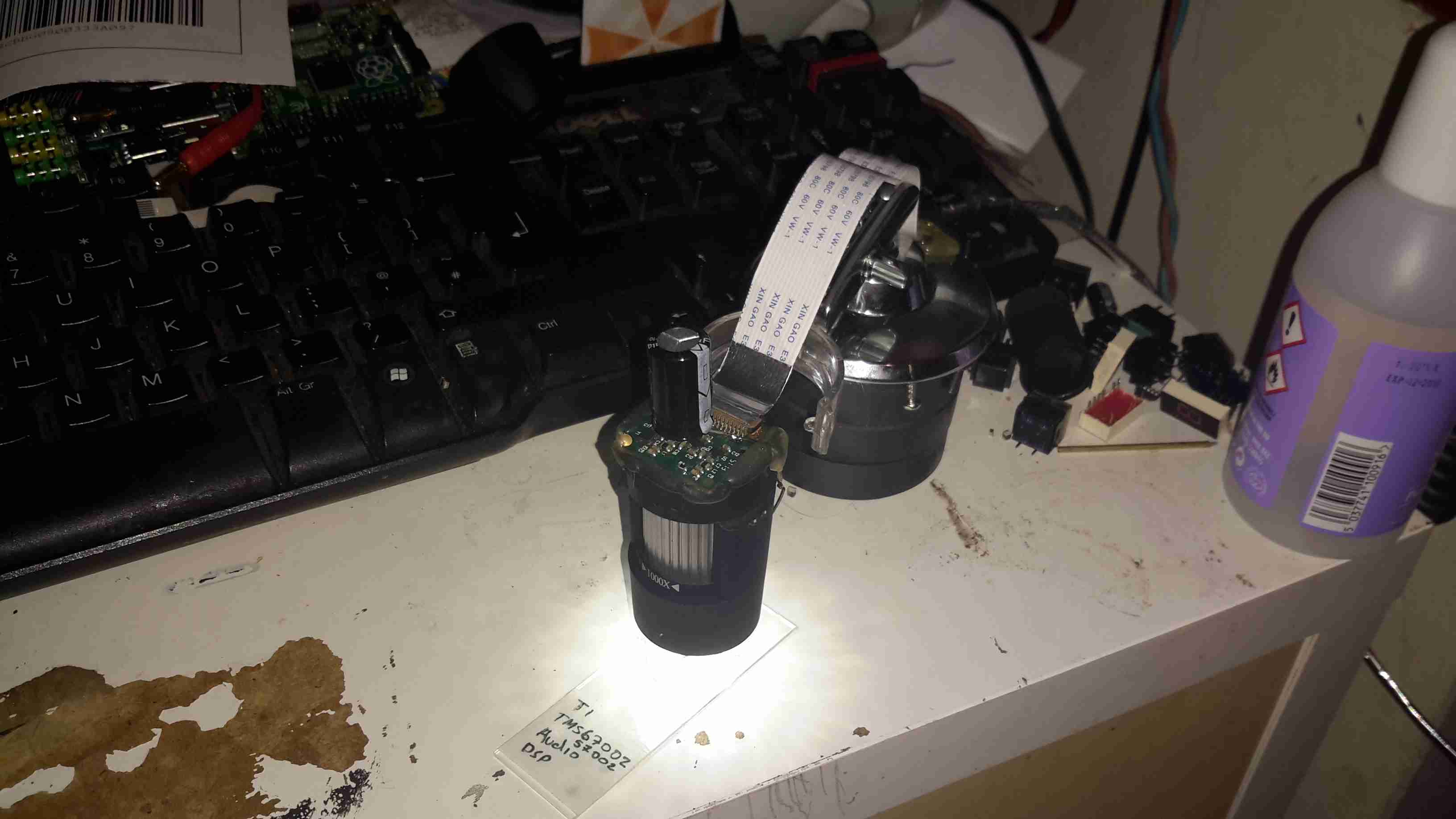
I had bought a cheap eBay USB microscope to get started, as I can’t currently afford a proper metallurgical microscope, but I found the resolution of 640×480 very poor. Some modification was required!
Modified Microscope
I’ve removed the original sensor board from the back of the optics assembly & attached a Raspberry Pi camera board. The ring that held the original sensor board has been cut down to a minimum, as the Pi camera PCB is slightly too big to fit inside.
The stock ring of LEDs is run direct from the 3.3v power rail on the camera, through a 4.7Ω resistor, for ~80mA. I also added a 1000µF capacitor across the 3.3v supply to compensate a bit for the long cable – when a frame is captured the power draw of the camera increases & causes a bit of voltage drop.
The stock lens was removed from the Pi camera module by careful use of a razor blade – being too rough here *WILL* damage the sensor die or the gold bond wires, which are very close to the edge of the lens housing, so be gentle!
Mounting Base
The existing mount for the microscope is pretty poor, so I’ve used a couple of surplus ceramic ring magnets as a better base, this also gives me the option of raising or lowering the base by adding or removing magnets.
To get more length between the Pi & the camera, I bought a 1-meter cable extension kit from Pi-Cables over at eBay, cables this long *definitely* require shielding in my space, which is a pretty aggressive RF environment, or interference appears on the display. Not surprising considering the high data rates the cable carries.
The FFC interface is hot-glued to the back of the microscope mount for stability, for handheld use the FFC is pretty flexible & doesn’t apply any force to the scope.
Die Photography
Since I modified the scope with a Raspberry Pi camera module, everything is done through the Pi itself, and the raspistill command.
Pi LCD
The command I’m currently using to capture the images is:
raspistill -ex auto -awb auto -mm matrix -br 62 -q 100 -vf -hf -f -t 0 -k -v -o CHIPNAME_%03d.jpg
This command waits between each frame for the ENTER key to be pressed, allowing me to position the scope between shots. Pi control & file transfer is done via SSH, while I use the 7″ touch LCD as a viewfinder.
The direct overhead illumination provided by the stock ring of LEDs isn’t ideal for some die shots, so I’m planning on fitting some off-centre LEDs to improve the resulting images.
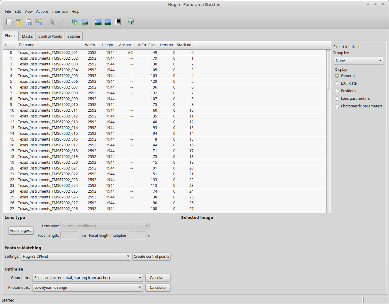
Image Processing
Obviously I can’t get an ultra-high resolution image with a single shot, due to the focal length, so I have to take many shots (30-180 per die), and stitch them together into a single image.
For this I use Hugin, an open-source panorama photo stitching package.
Hugin
Here’s Hugin with the photos loaded in from the Raspberry Pi. To start with I use Hugin’s built in CPFind to process the images for control points. The trick with getting good control points is making sure the images have a high level of overlap, between 50-80%, this way the software doesn’t get confused & stick the images together incorrectly.
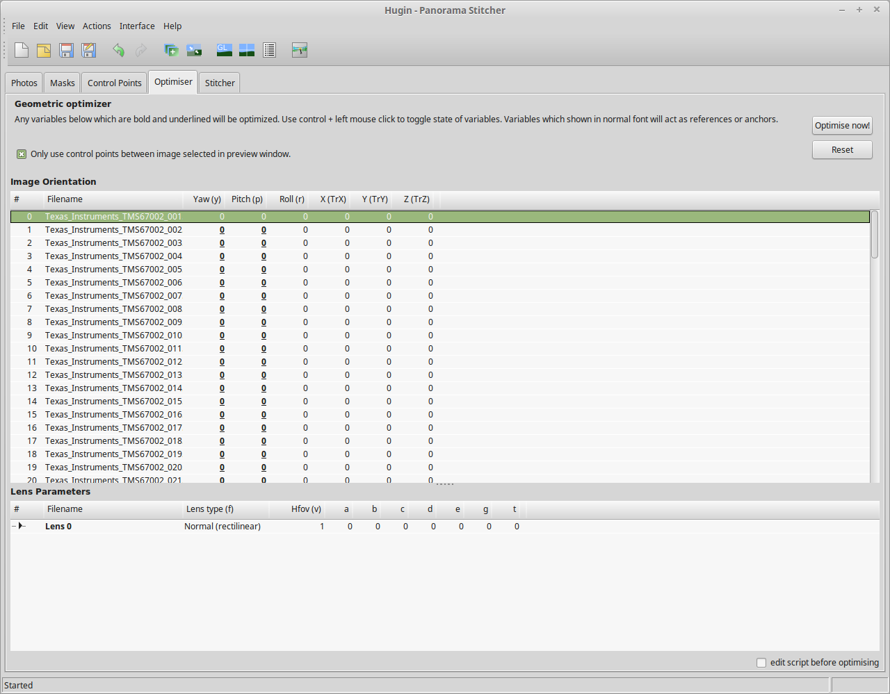
Optimiser
After the control points are generated, which for a large number of high resolution images can take some time, I run the optimiser with only Yaw & Pitch selected for all images.
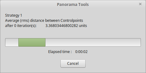
Optimising
If all goes well, the resulting optimisation will get the distance between control points to less than 0.3 pixels.
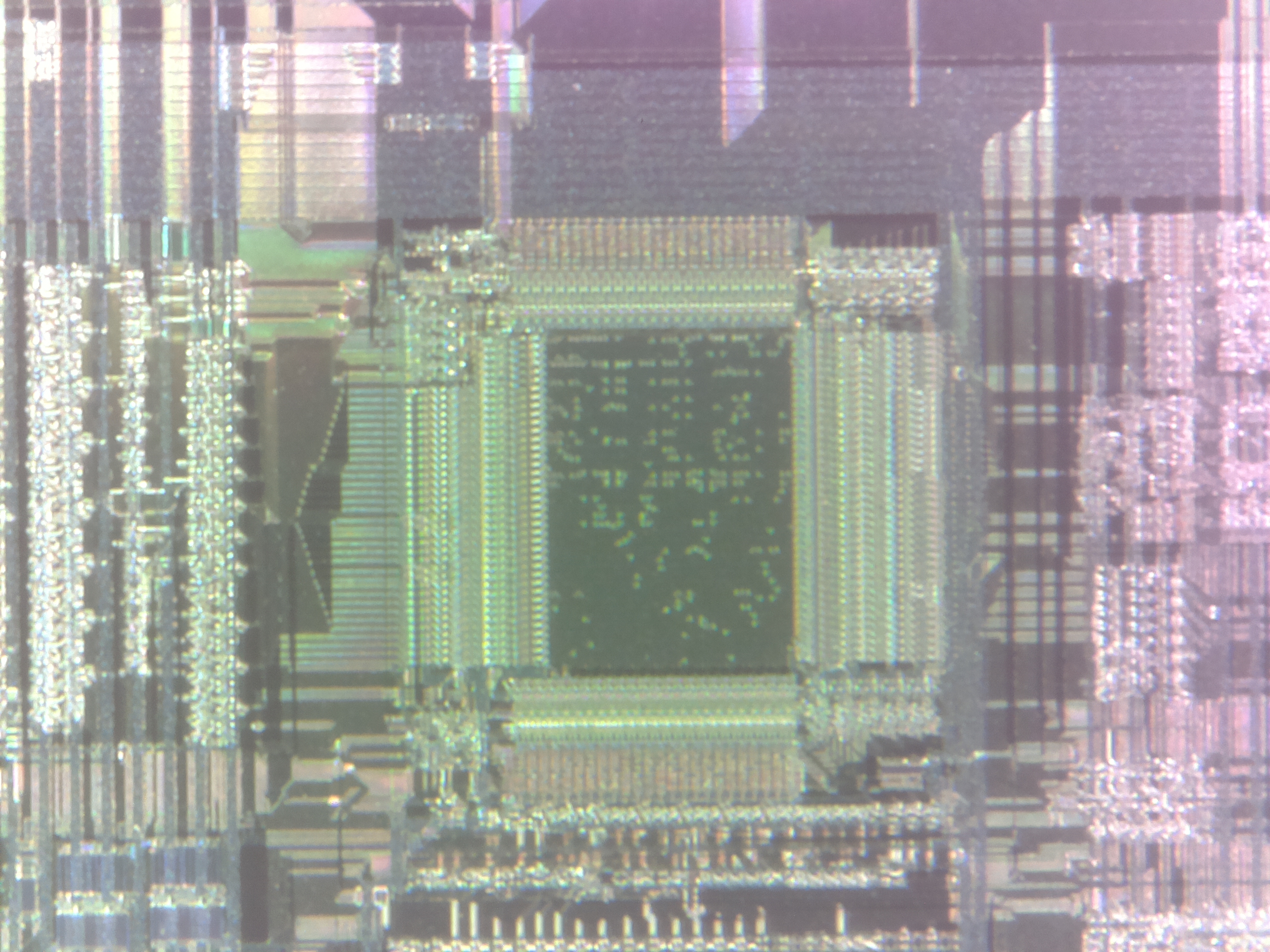
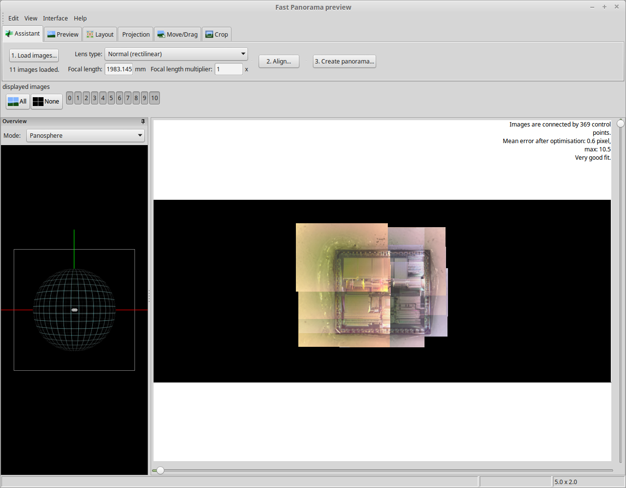
Panorama Preview
After the control points & optimisation is done, the resulting image can be previewed before generation.
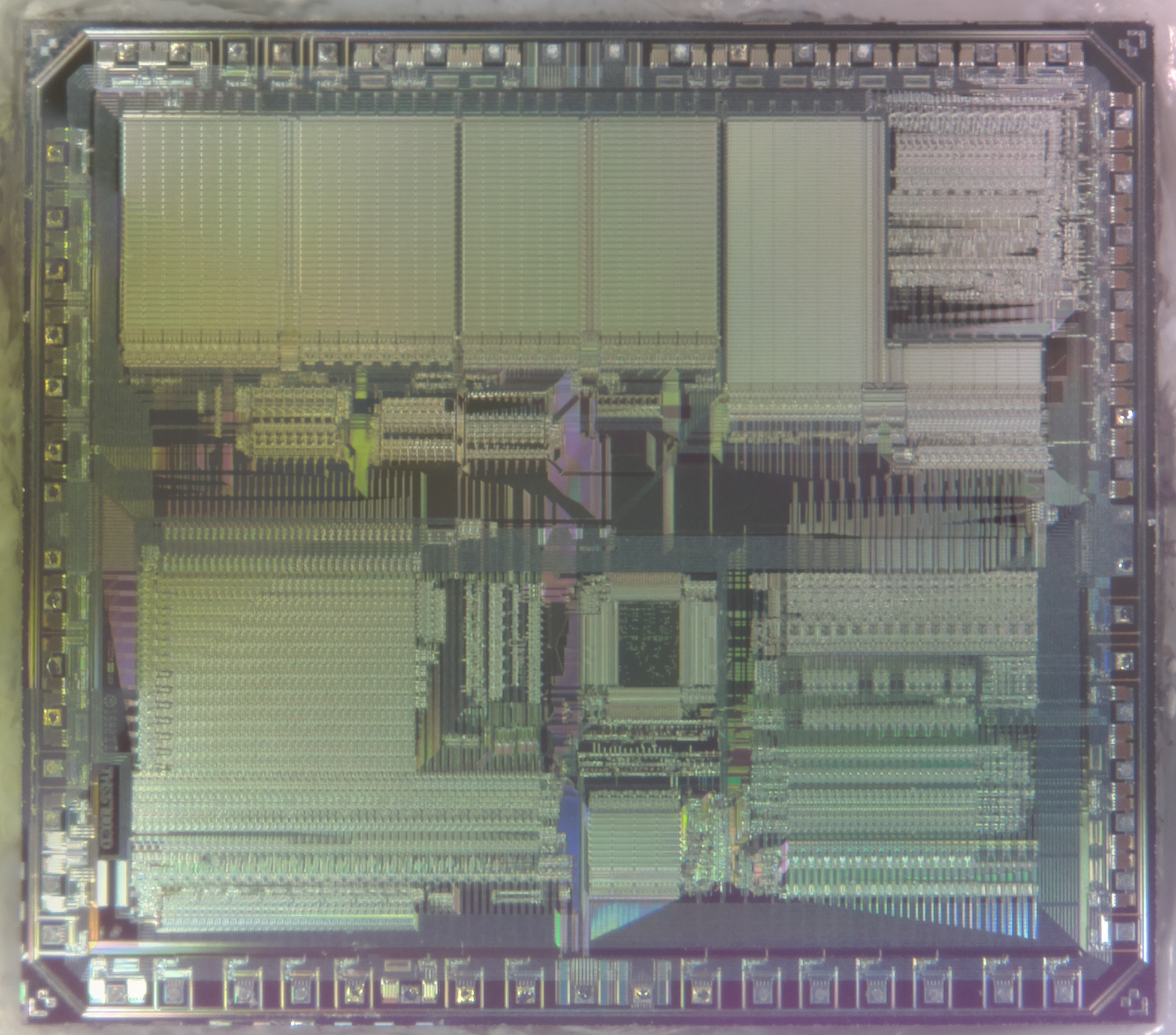
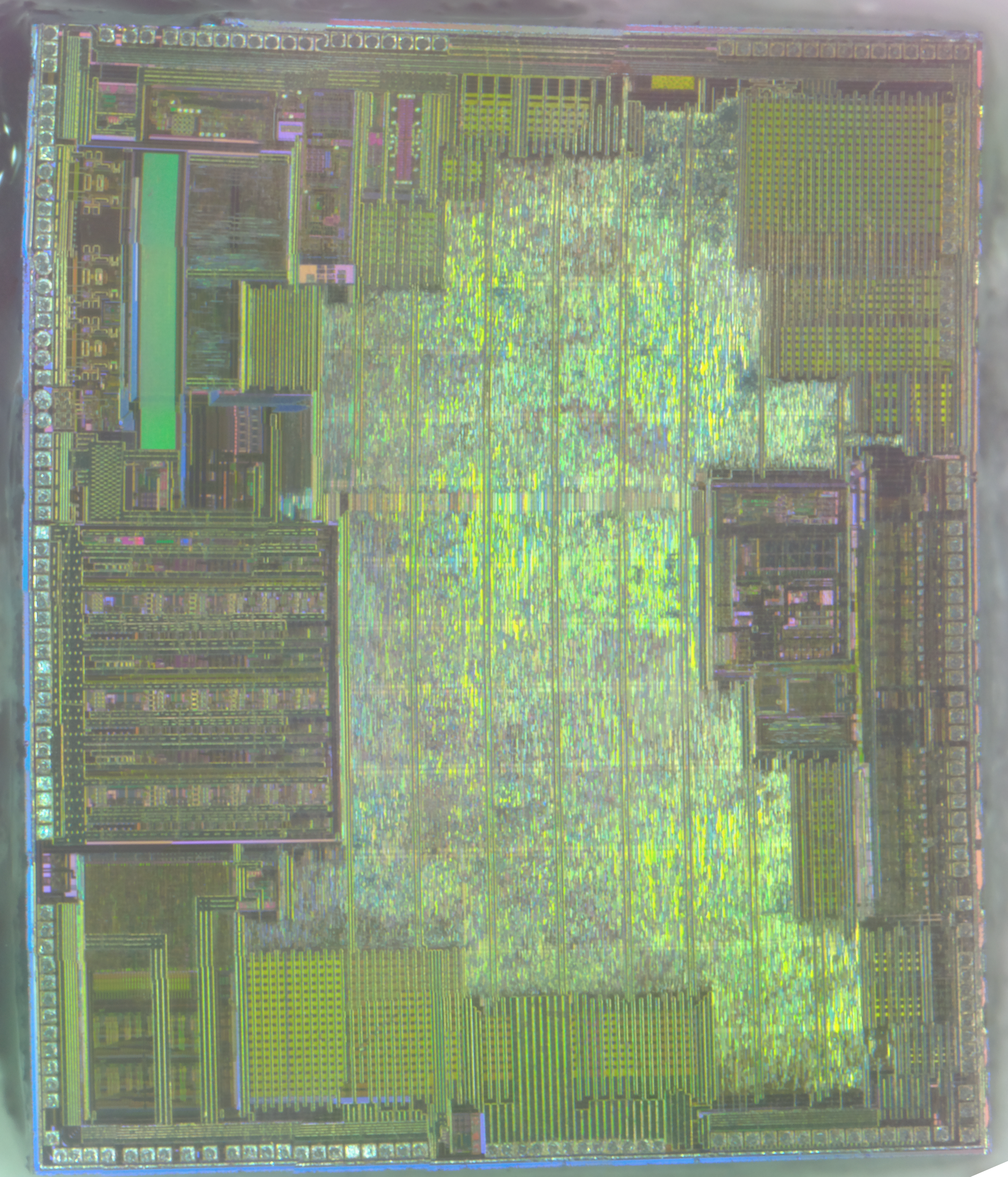
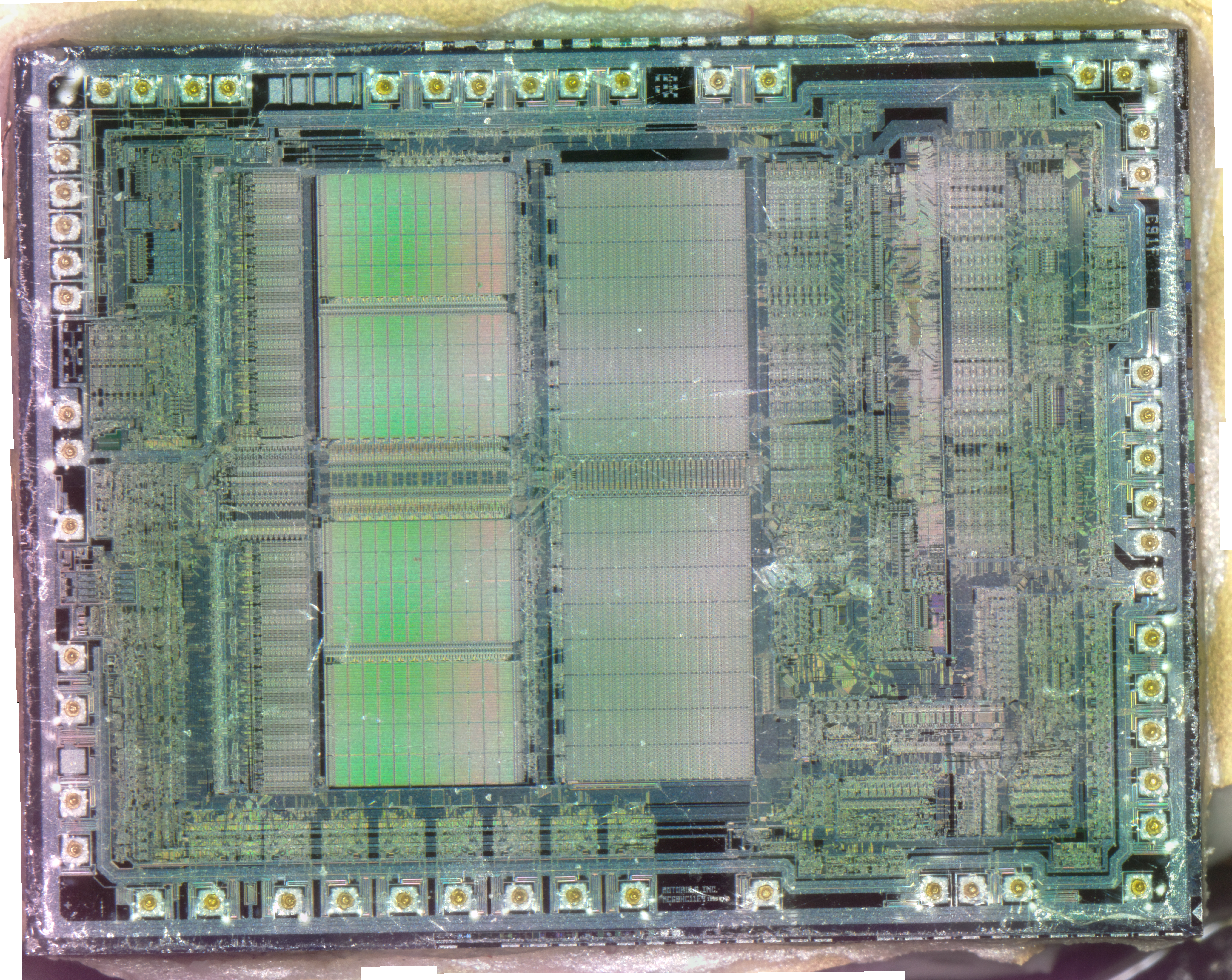
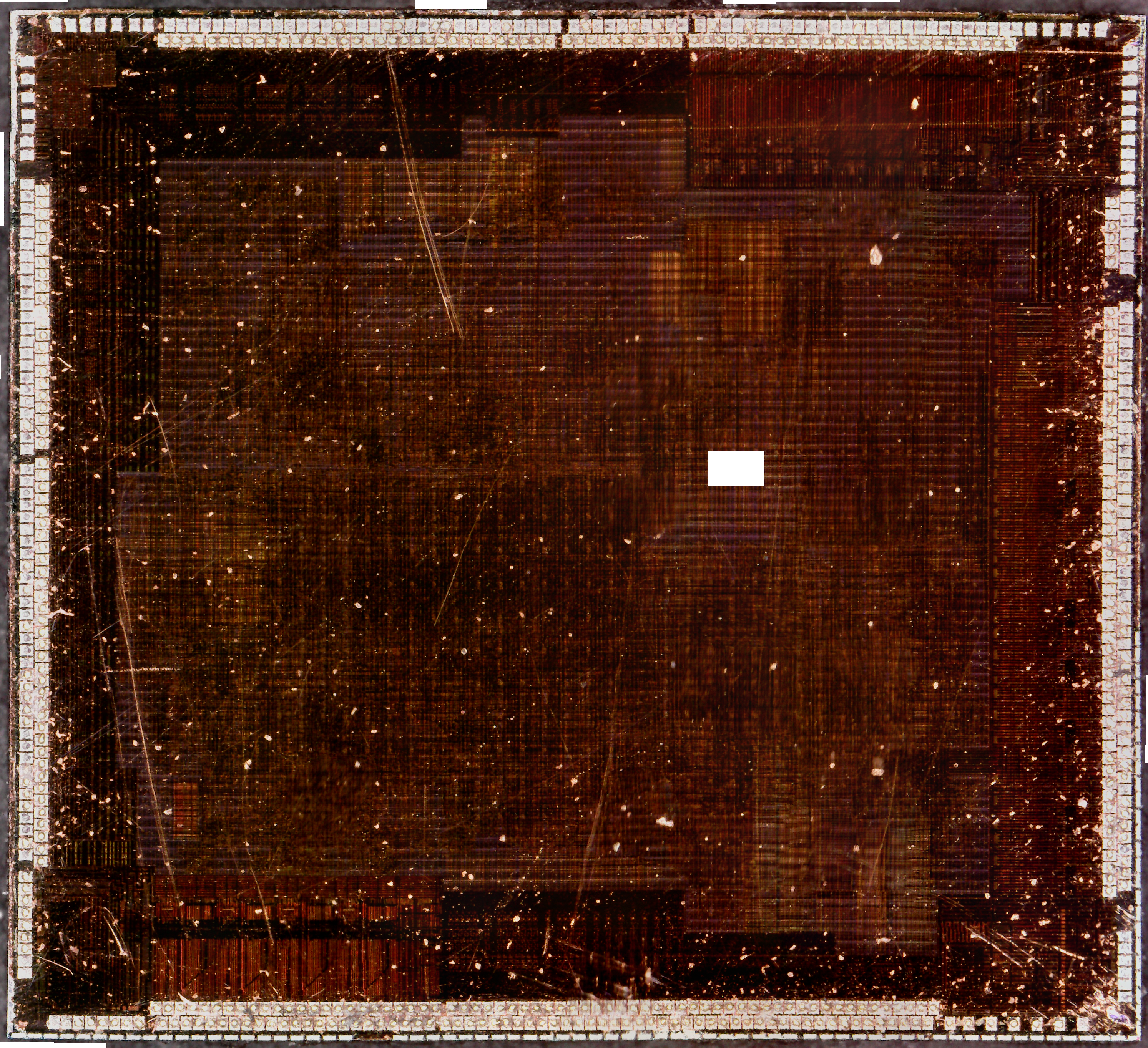
Texas Instruments TMS67002
After all the image processing, the resulting die image should look something like the above, with no noticeable gaps.
This particular IC came out of a very old VHF band radio, from the early 90’s. The die was encased in a custom ceramic package, like every other IC in the radio, with a custom part number. I managed to identify it from the markings on the silicon.
Motorola MC68HC11L6
This was a pretty powerful MCU for it’s time, with 16K of onboard ROM, 512 bytes of both RAM & EEPROM, a 16-bit timer, 8-bit ADC, SPI & a MC68HC11 CPU core.
If you’ve found my content useful, please consider leaving a donation by clicking the Tip Jar below!
All collected funds go towards new content & the costs of keeping the server online.