As with the previous Sony Watchman hack, injecting a composite video signal into this one is just as easy. I desoldered both the VIF/SIF IC & the digital tuner control (the tuner controller was still injecting it’s indicator into the video circuitry with the IF IC disconnected).
Composite video is on pin 18 of the Video IF IC, with the audio on Pin 13.
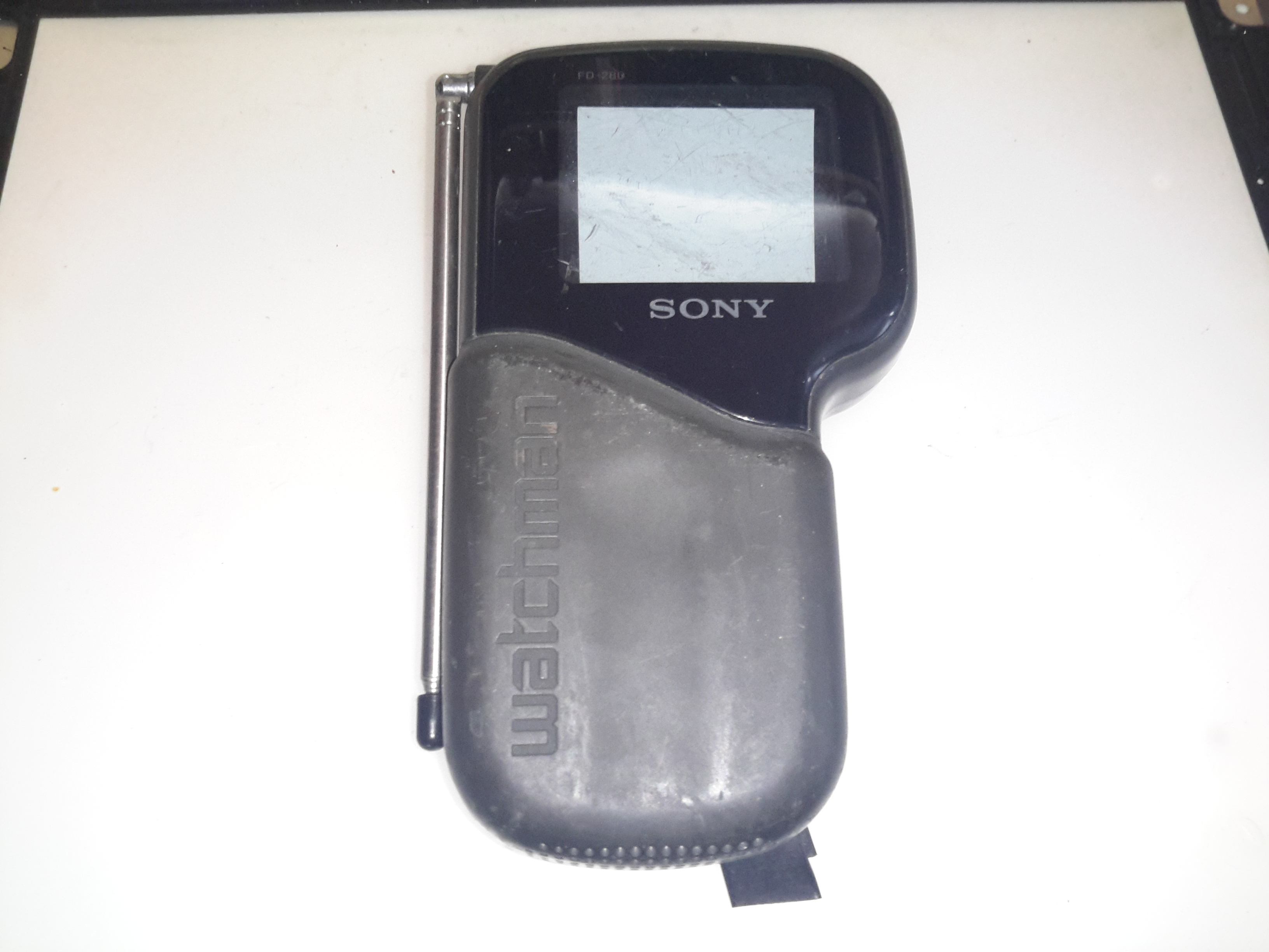
Here’s another Sony Flat CRT TV, the FD0280. This one was apparently the last to use CRT technology, later devices were LCD based. This one certainly doesn’t feel as well made as the last one, with no metal parts at all in the frame, just moulded plastic.
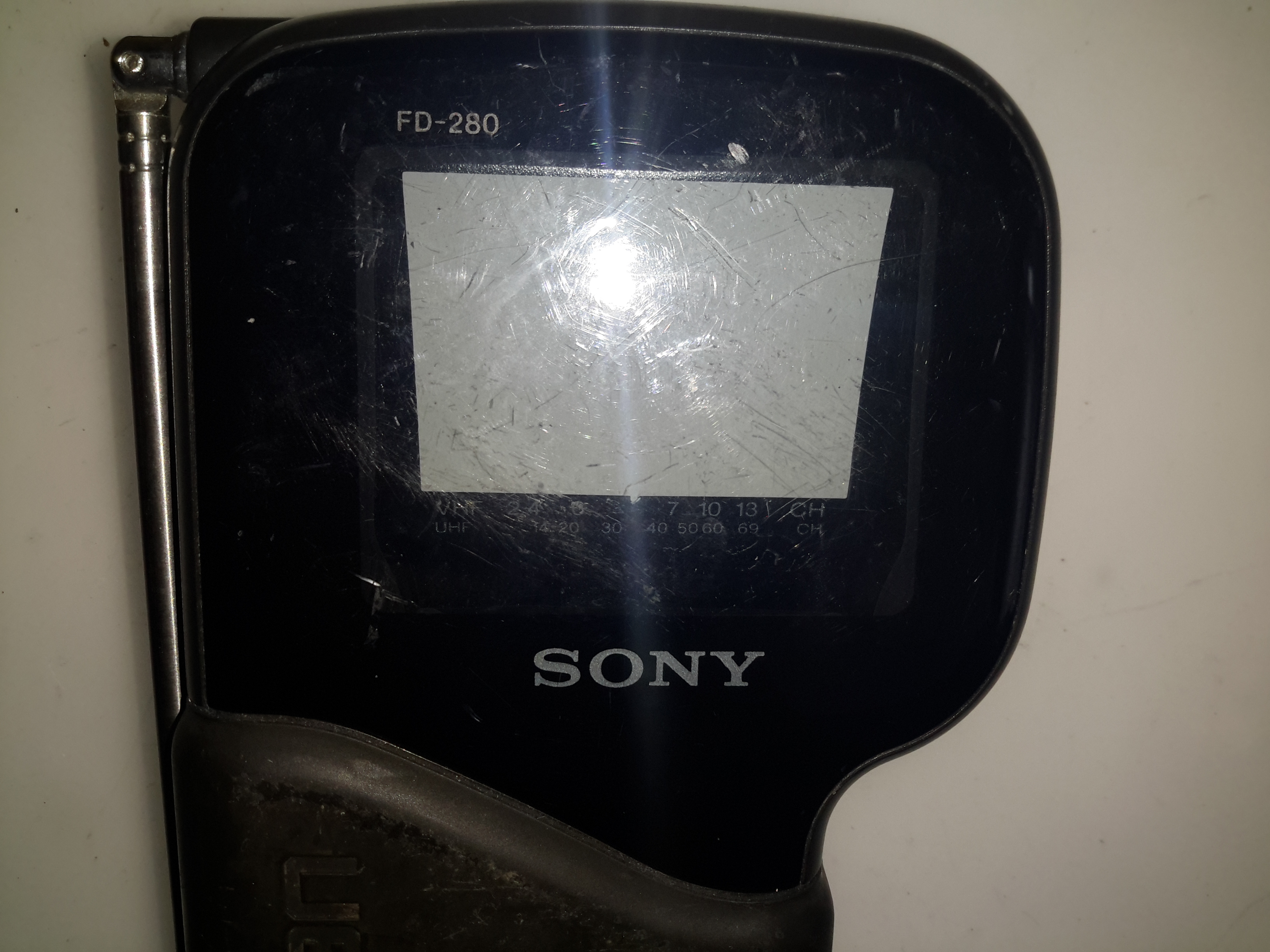
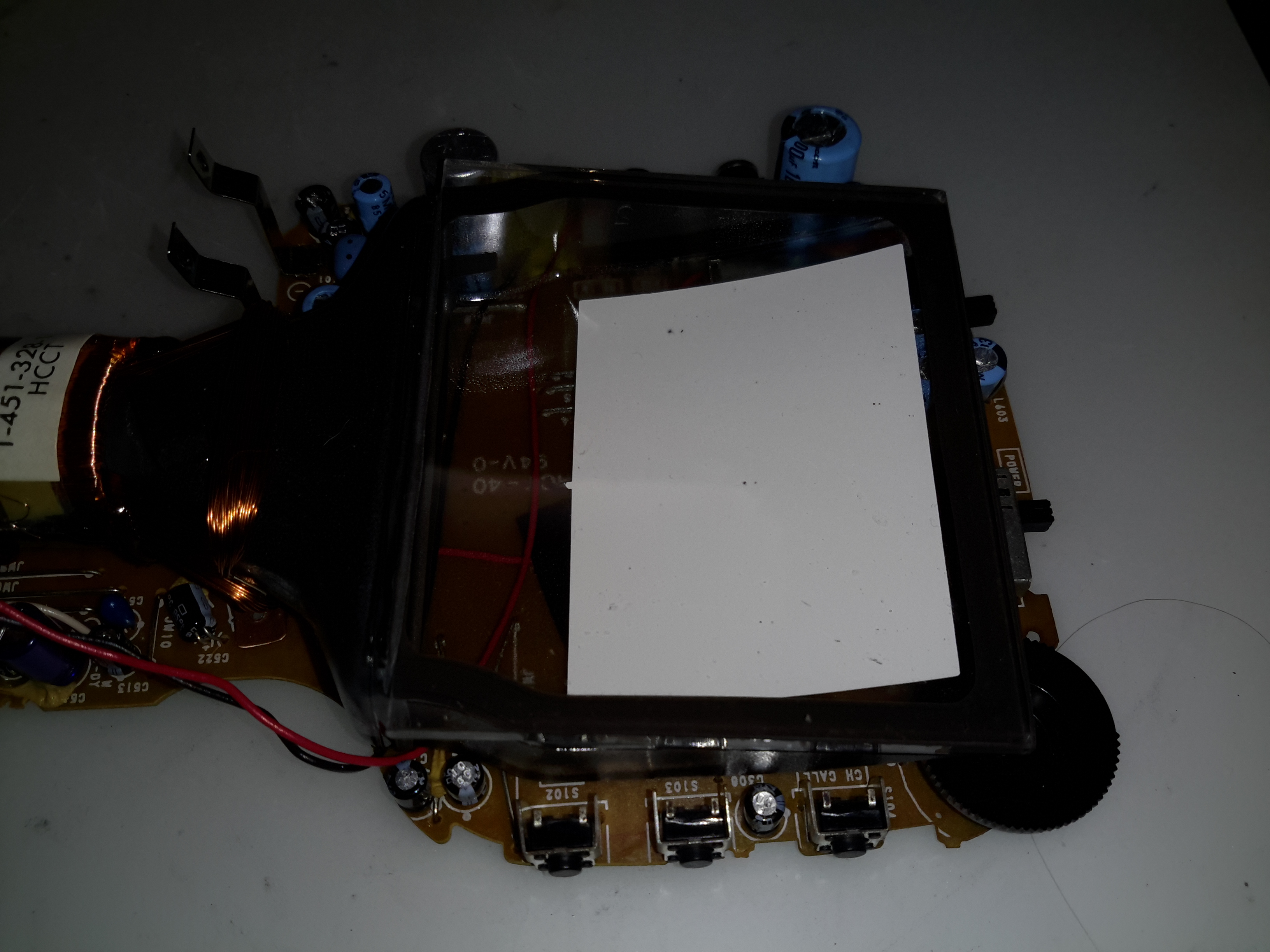
CRT Screen
Being a later model, this one has a much larger screen.
Autotuning
Instead of the manual tuner of the last Watchman, this one has automatic tuning control, to find the local stations.
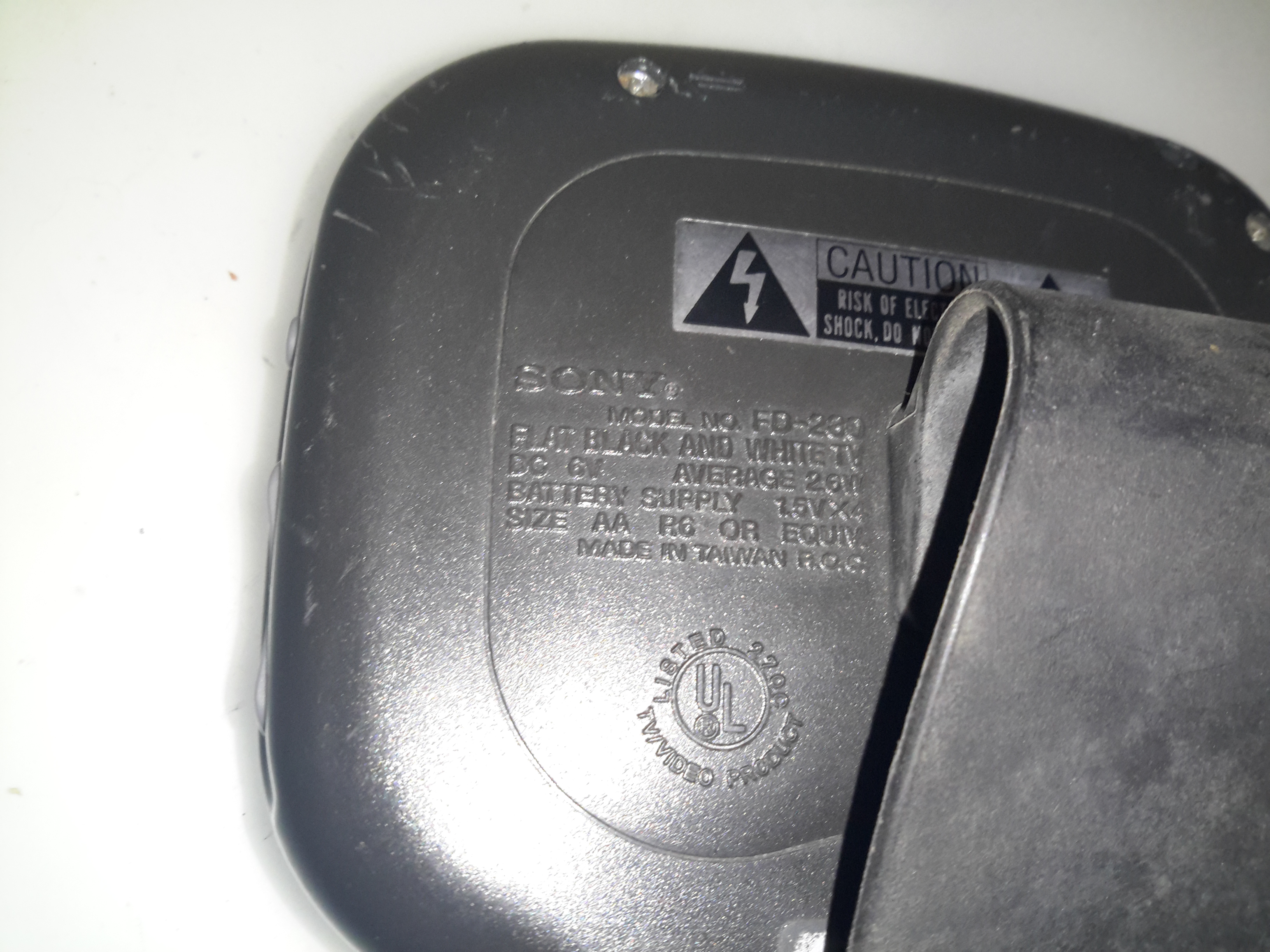
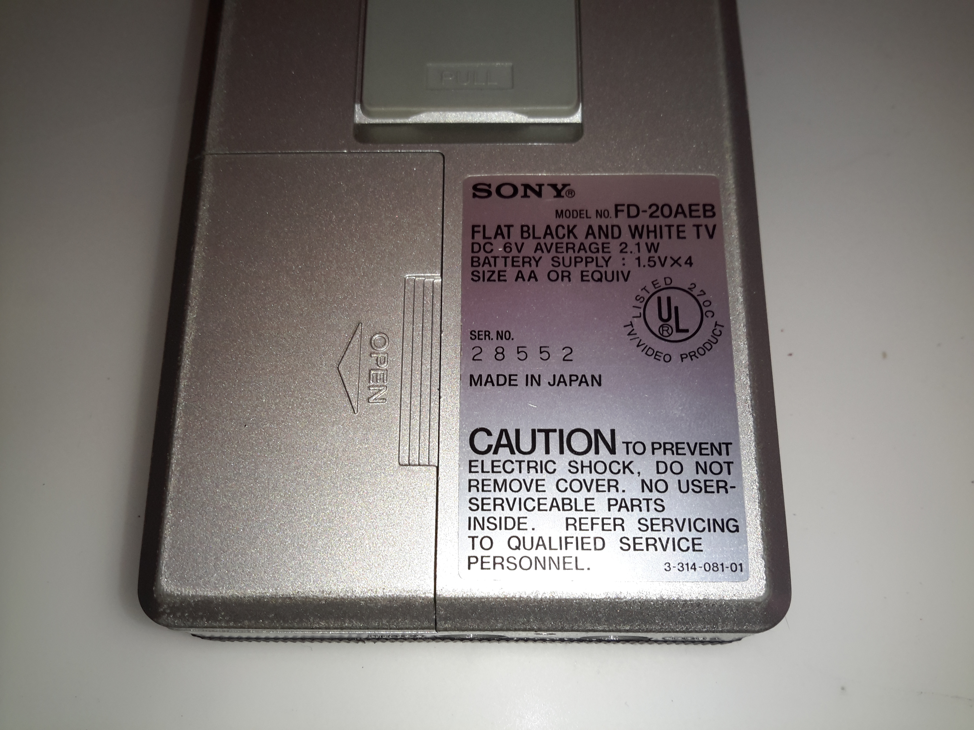
Spec Label
The spec puts the power consumption a little higher than the older TV, this isn’t surprising as the CRT screen is bigger & will require higher voltages on the electrodes.
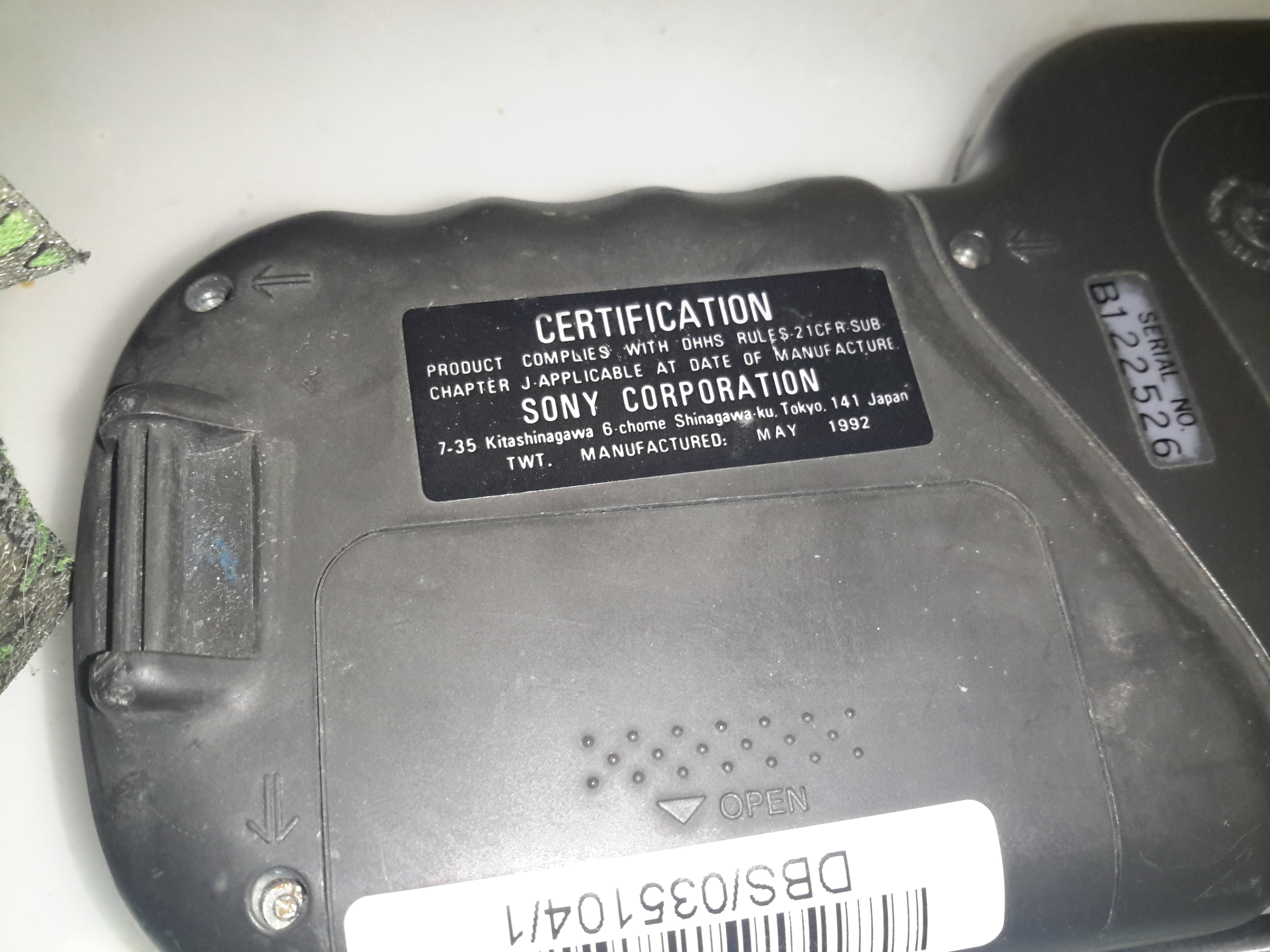
Certification Label
The certification label dates this model to May 1992.
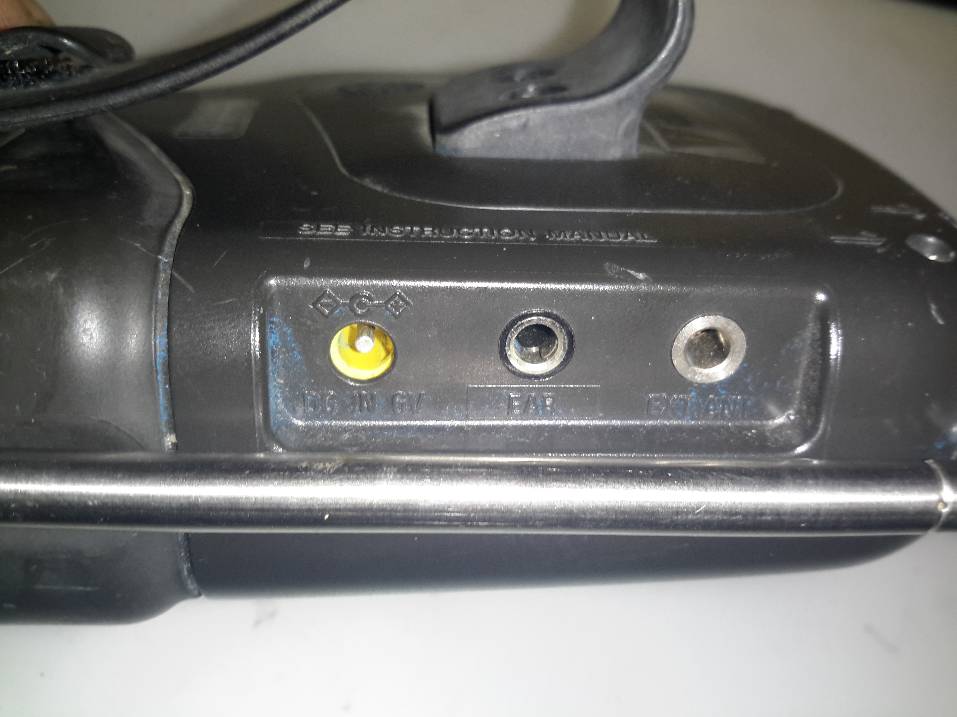
External Inputs
Still not much in the way of inputs on this TV. There’s an external power input, external antenna input & a headphone jack. No composite from the factory. (Hack incoming ;)).
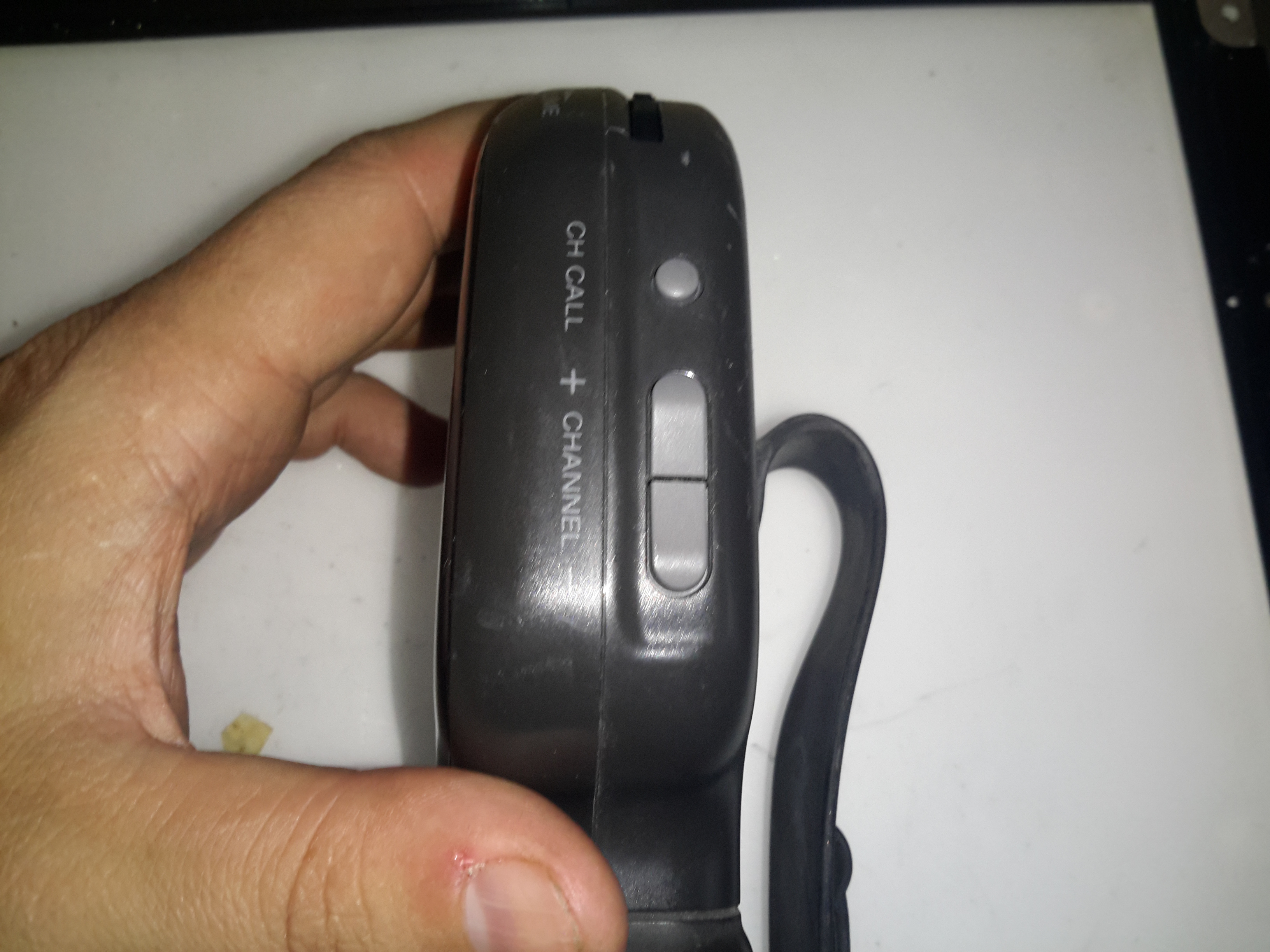
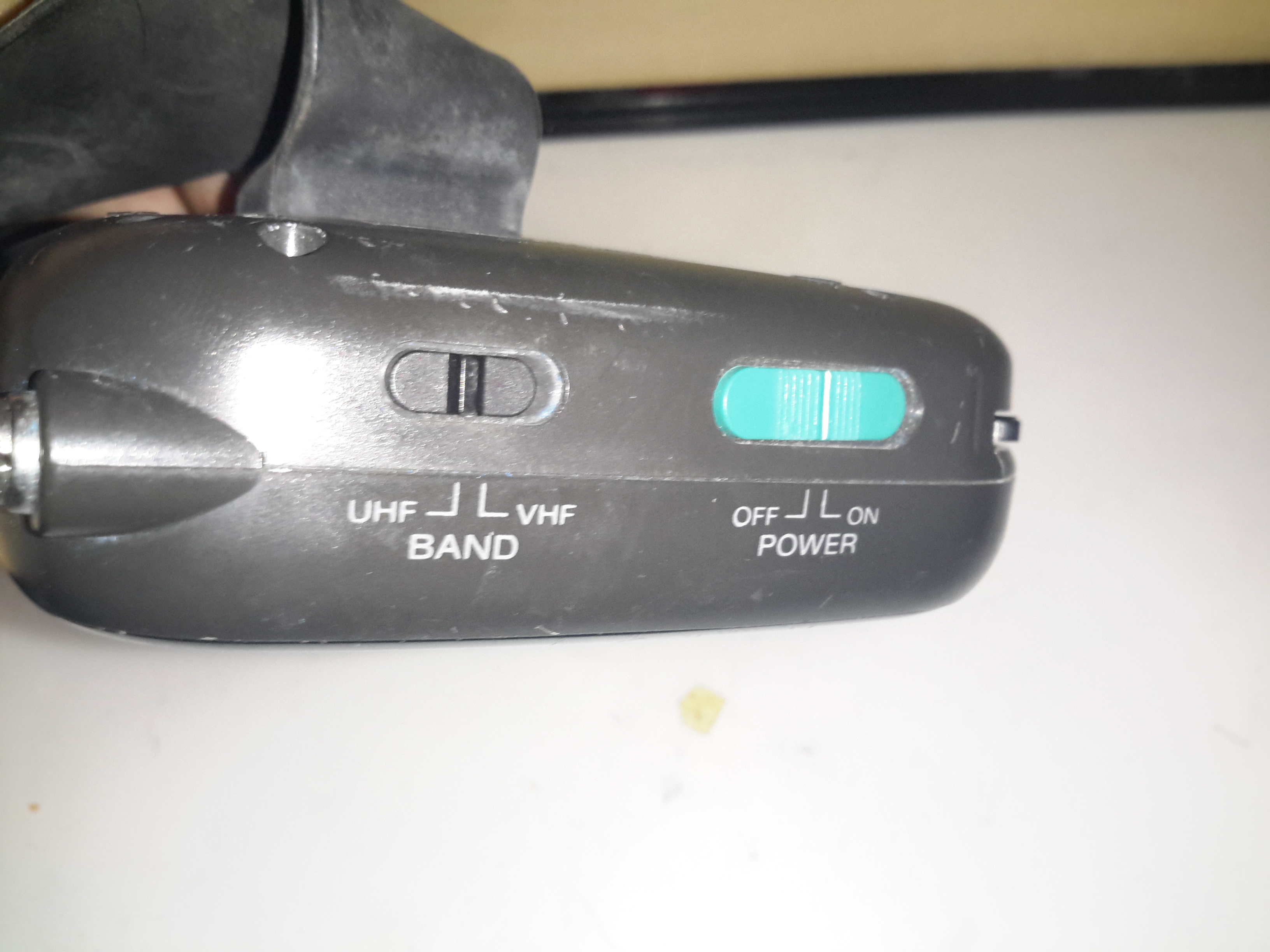
Power / Band
The UHF/VHF & power switches are on the top of this model.
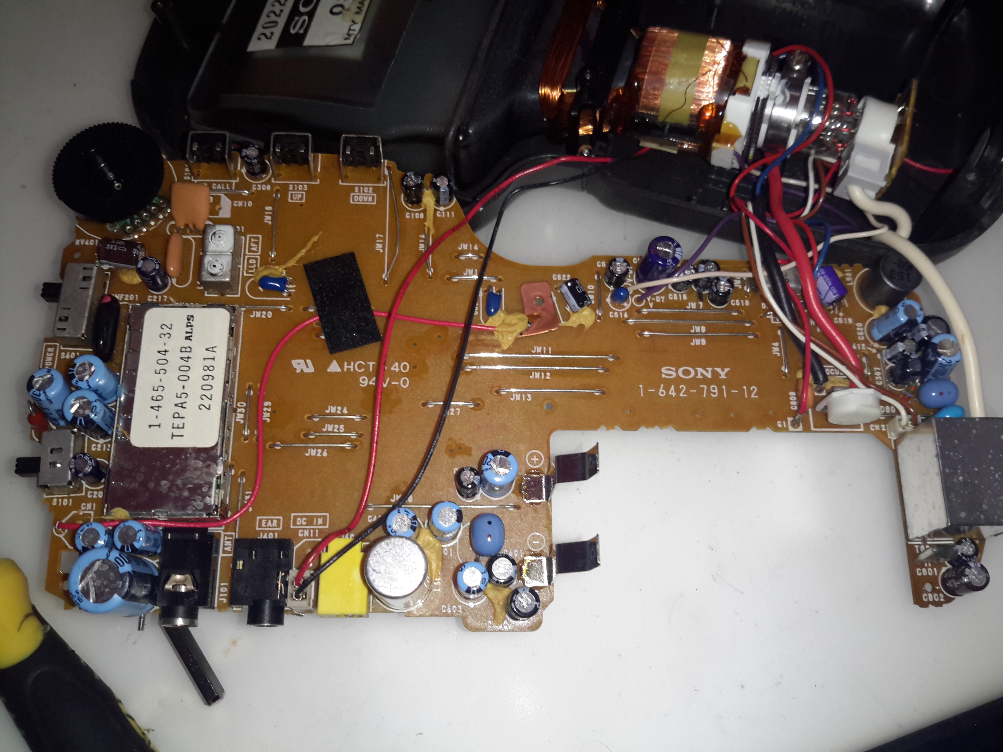
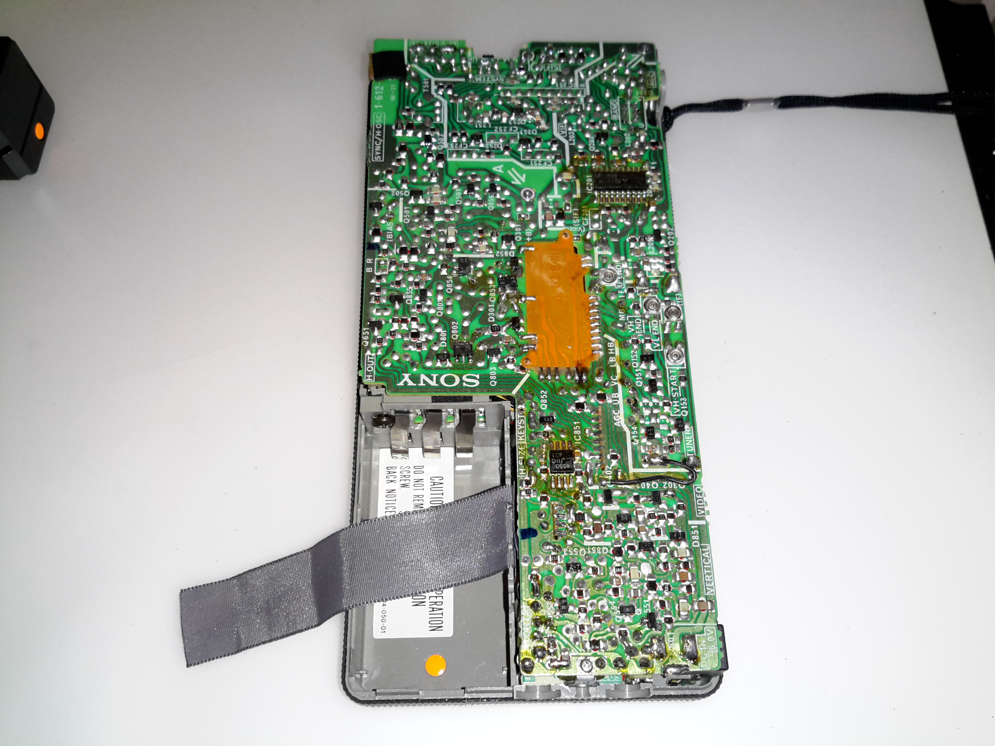
Back Cover Removed
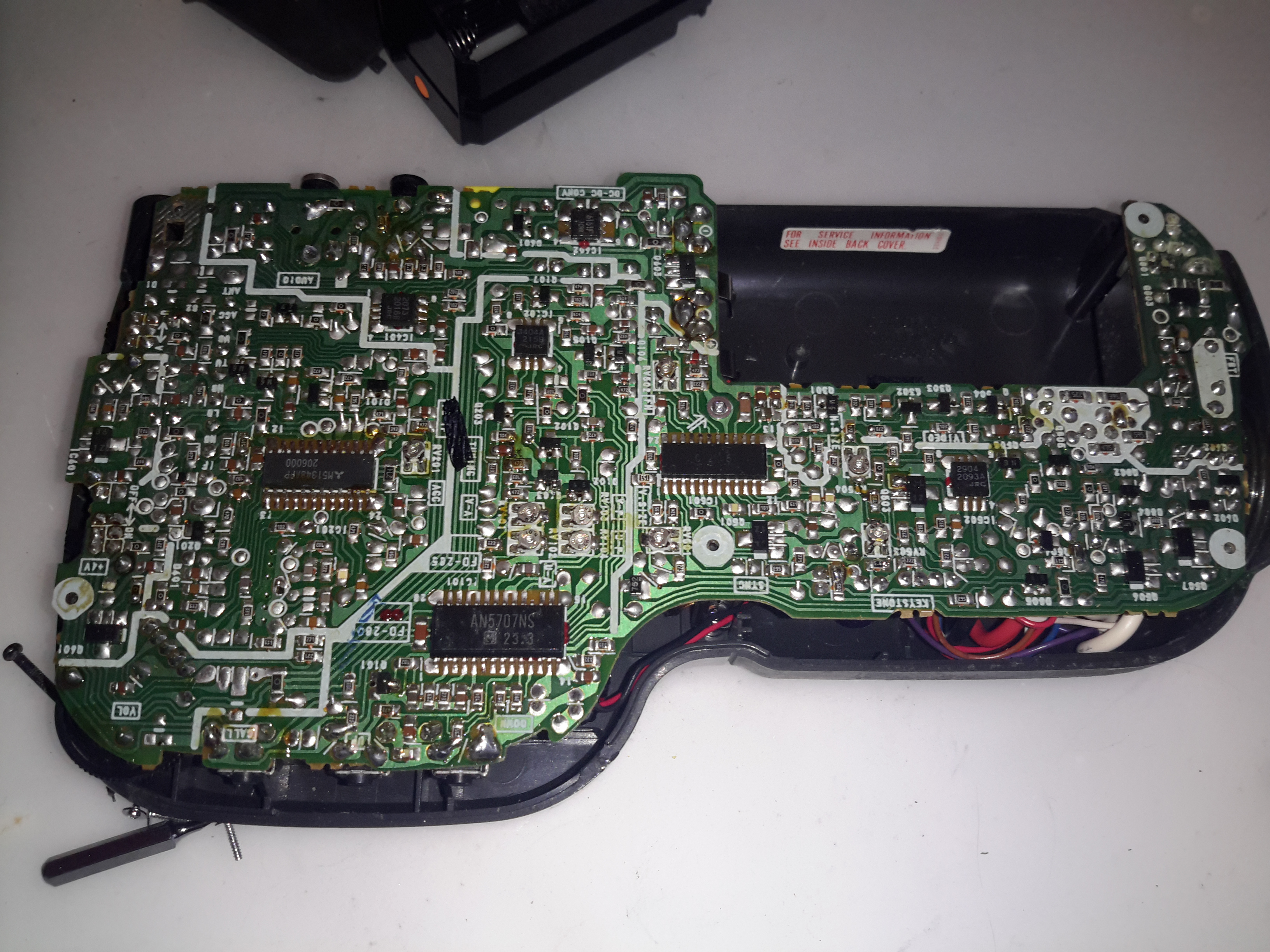
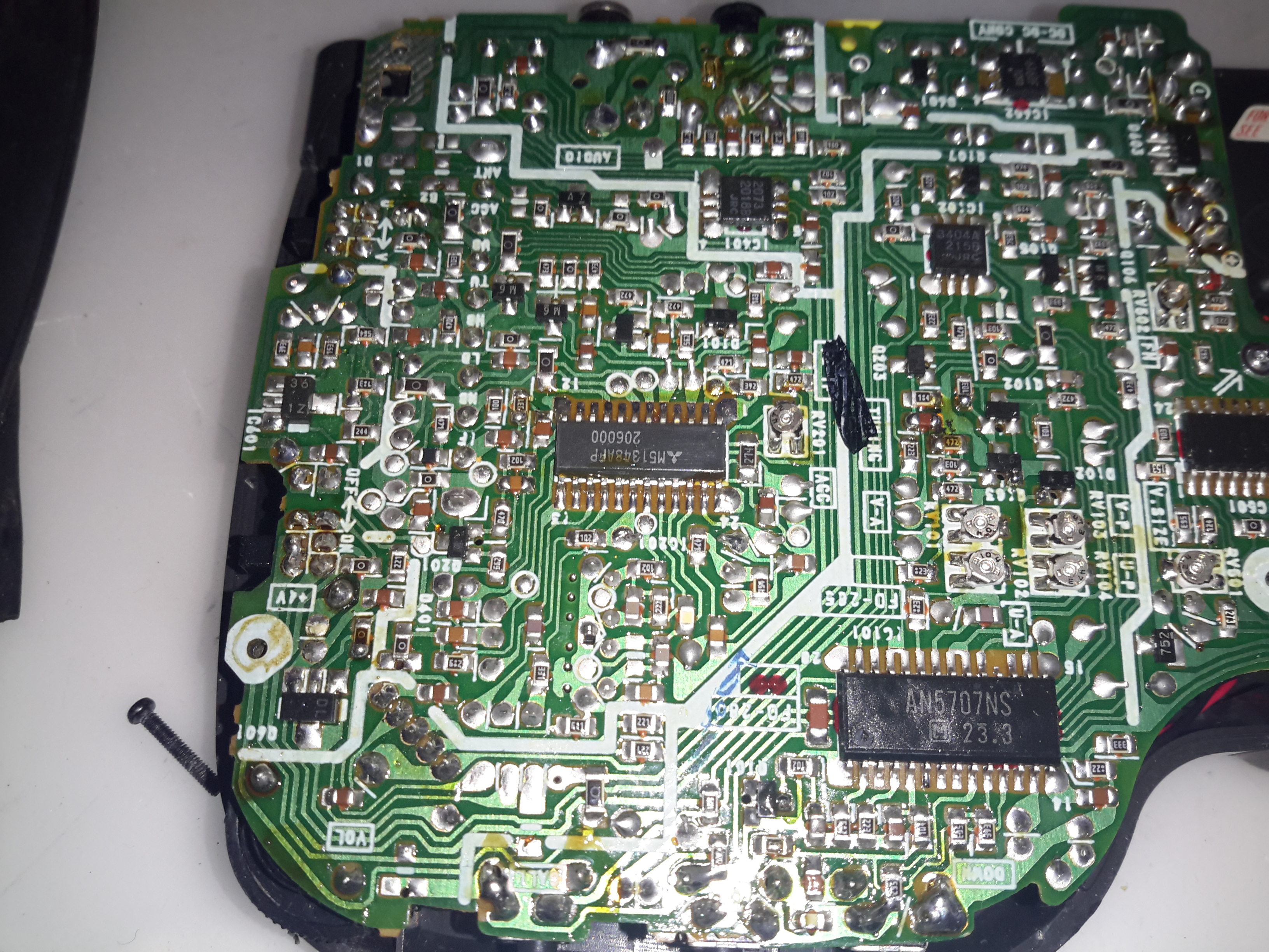
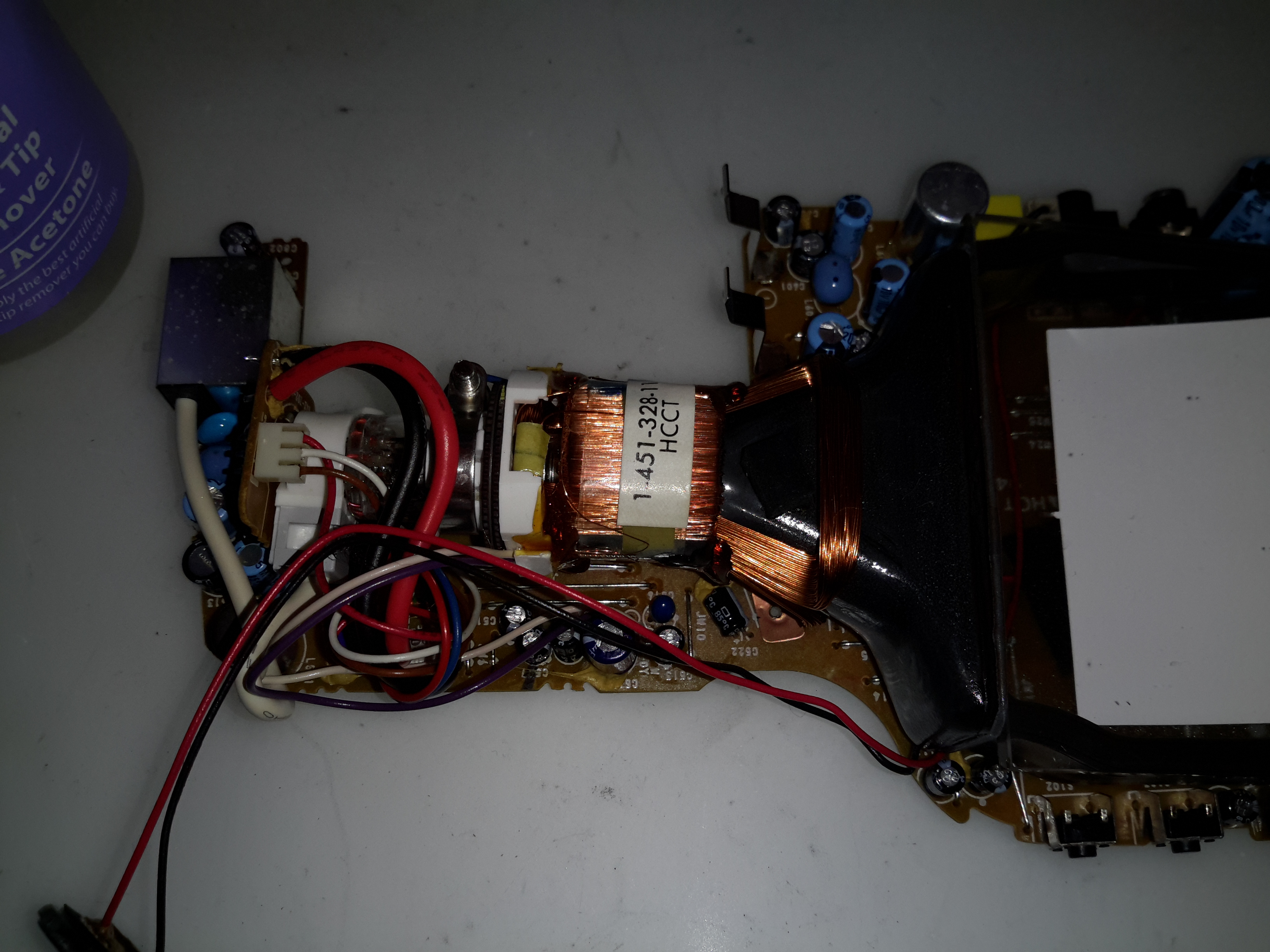
Removing some very tiny screws allows the back to be removed. There’s significant difference in this model to the last, more of the electronics are integrated into ICs, nearly everything is SMD.
RF Section
There’s the usual RF tuner section & IF, in this case the VIF/SIF is a Mitsubishi M51348AFP.
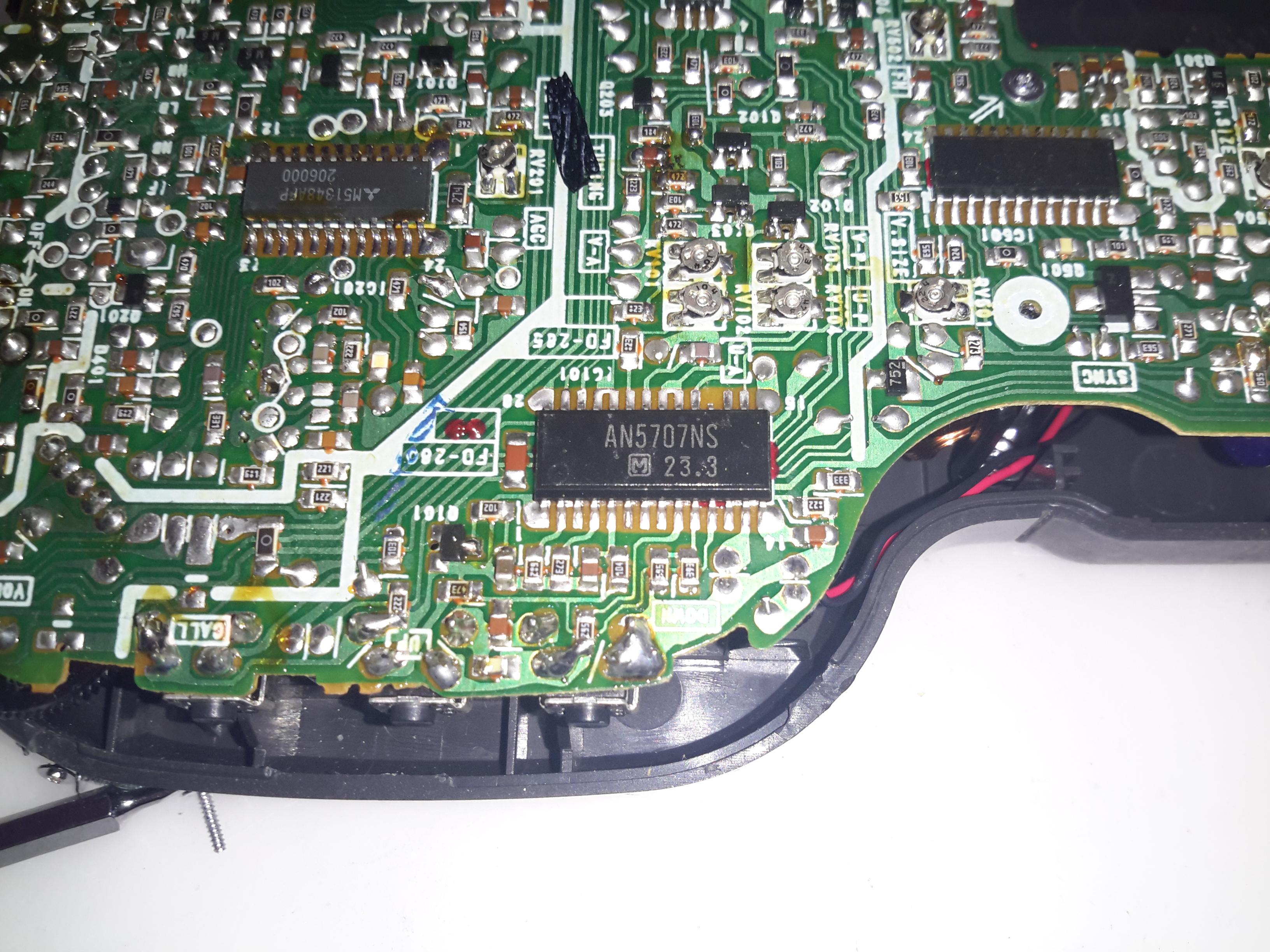
Tuner Controller
The digital control of the tuner is perfomed by this Panasonic AN5707NS.
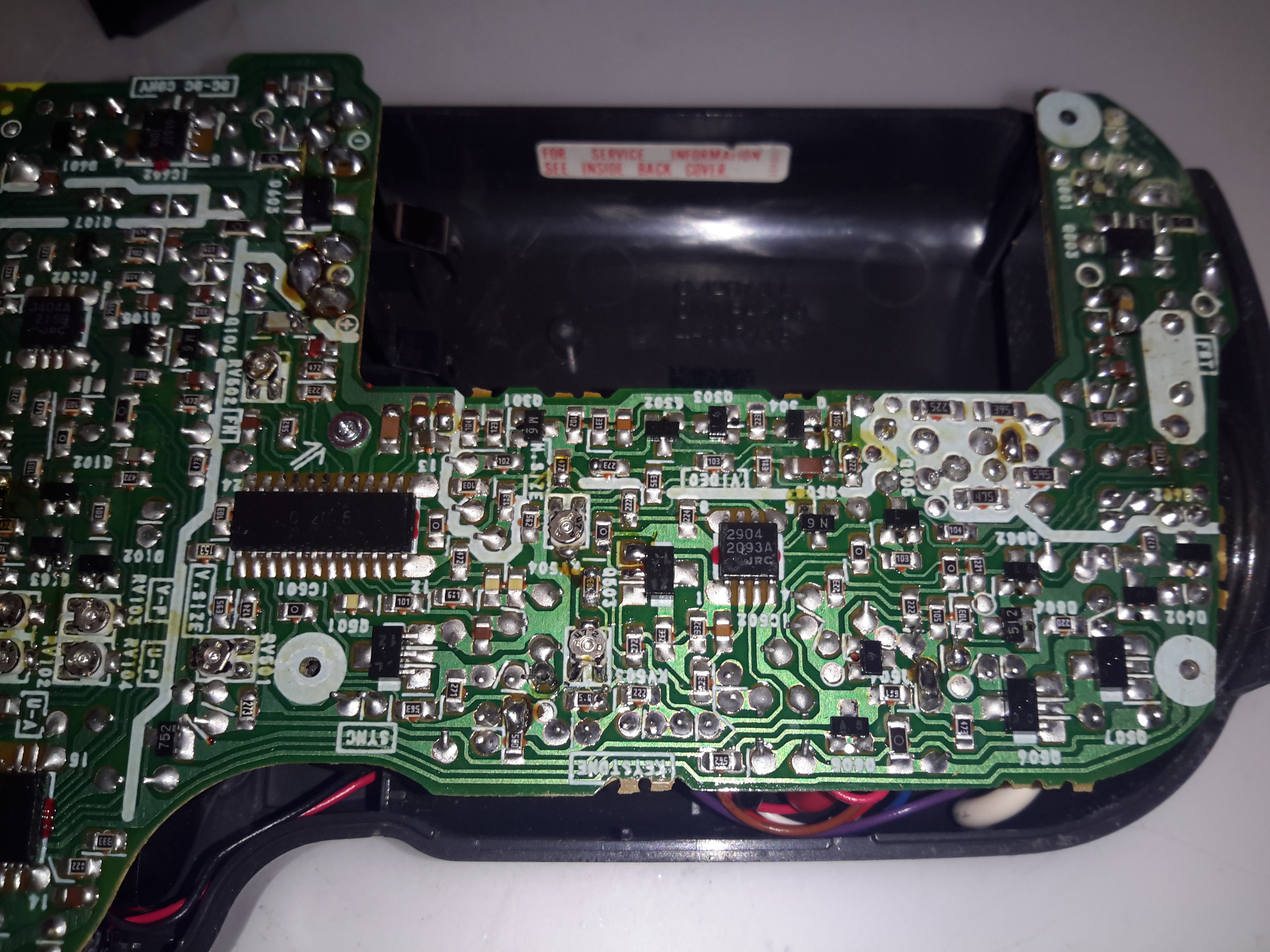
Deflection / Sync
The deflection & sync functions appear to be controlled by a single Sony branded custom IC, the CX20157. Similar to many other custom Sony ICs, a datasheet for this wasn’t forthcoming.
PCB Top
There’s very little on the top side of the board, the RF section is on the left, there’s a DC-DC converter bottom centre next to the battery contacts. This DC-DC converter has a very unusual inductor, completely encased in a metal can. This is probably done to prevent the magnetic field from interfering with the CRT.
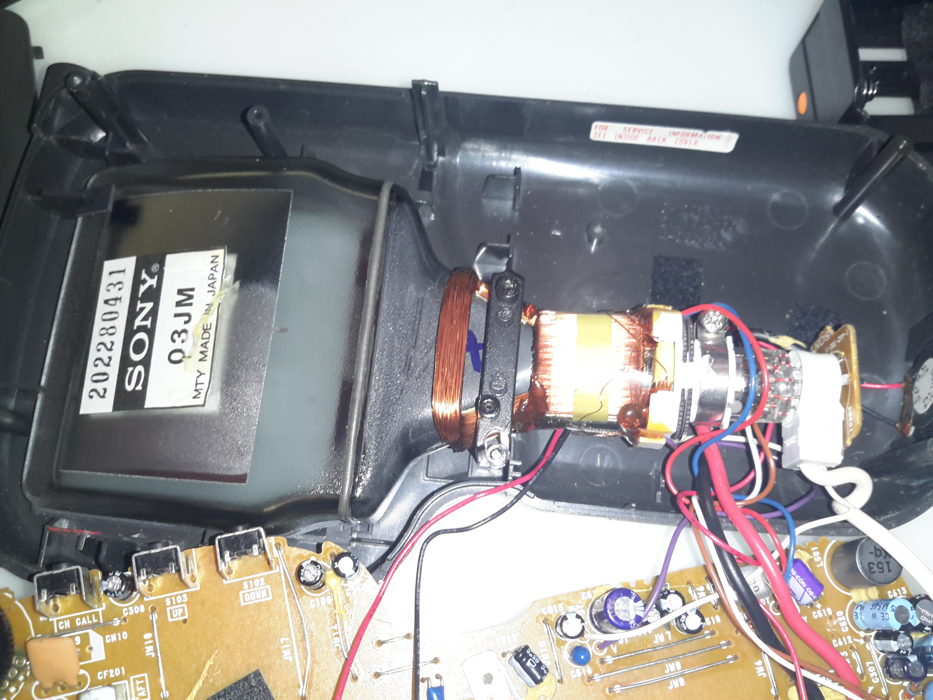
CRT
Here’s the CRT itself, the Sony 03-JM. The back of this CRT is uncoated at the bottom, the tuning scale was taped to the back so it lined up with the tuning bar displayed on the screen.
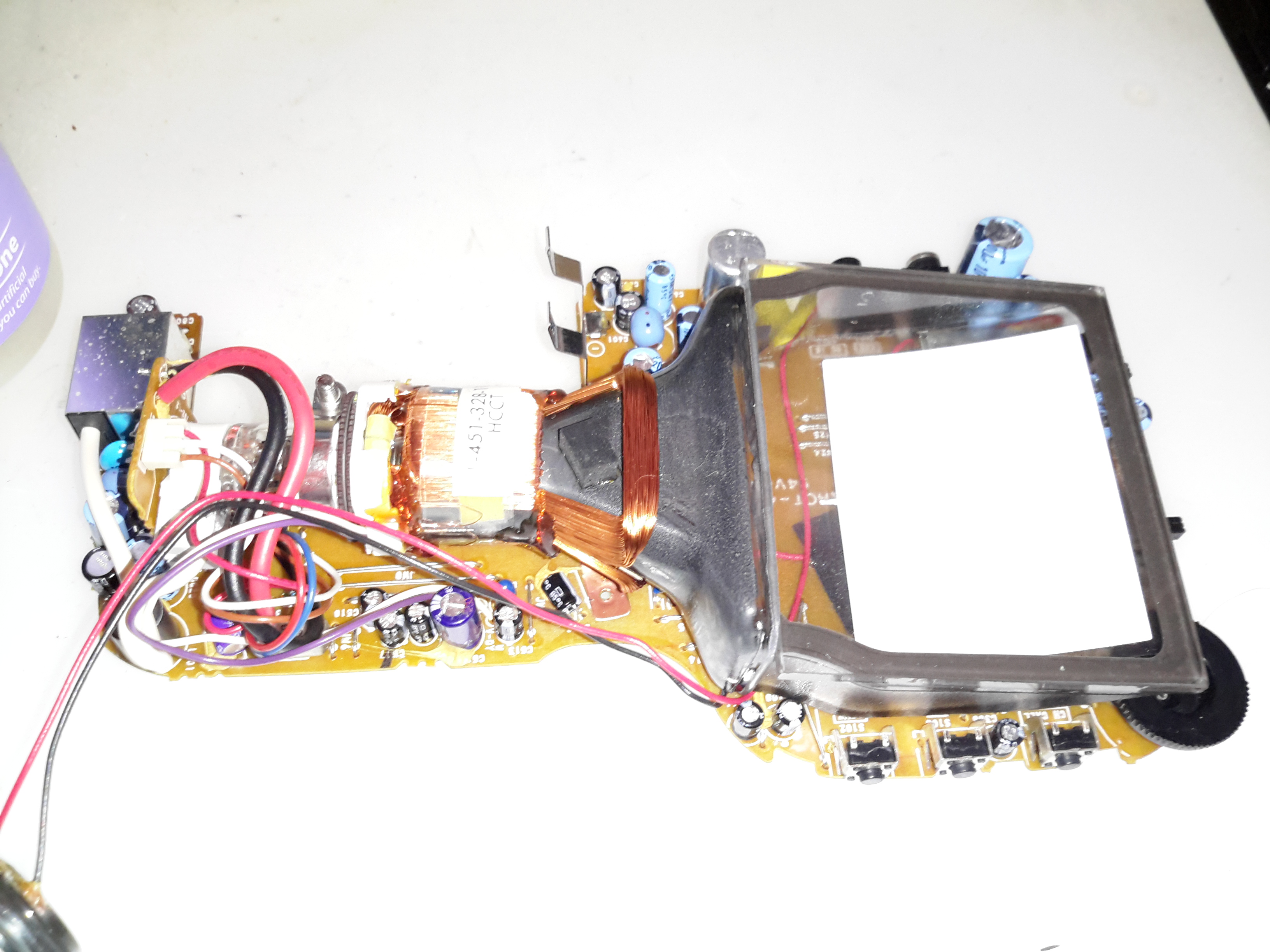
Electronics
Here’s the electronics completely removed from the shell. There’s much more integration in this model, everything is on a single PCB.
Phosphor Screen
The curve in the phosphor screen can clearly be seen here. This CRT seems to have been cost-reduced as well, with the rough edges on the glass components having been left unfinished.
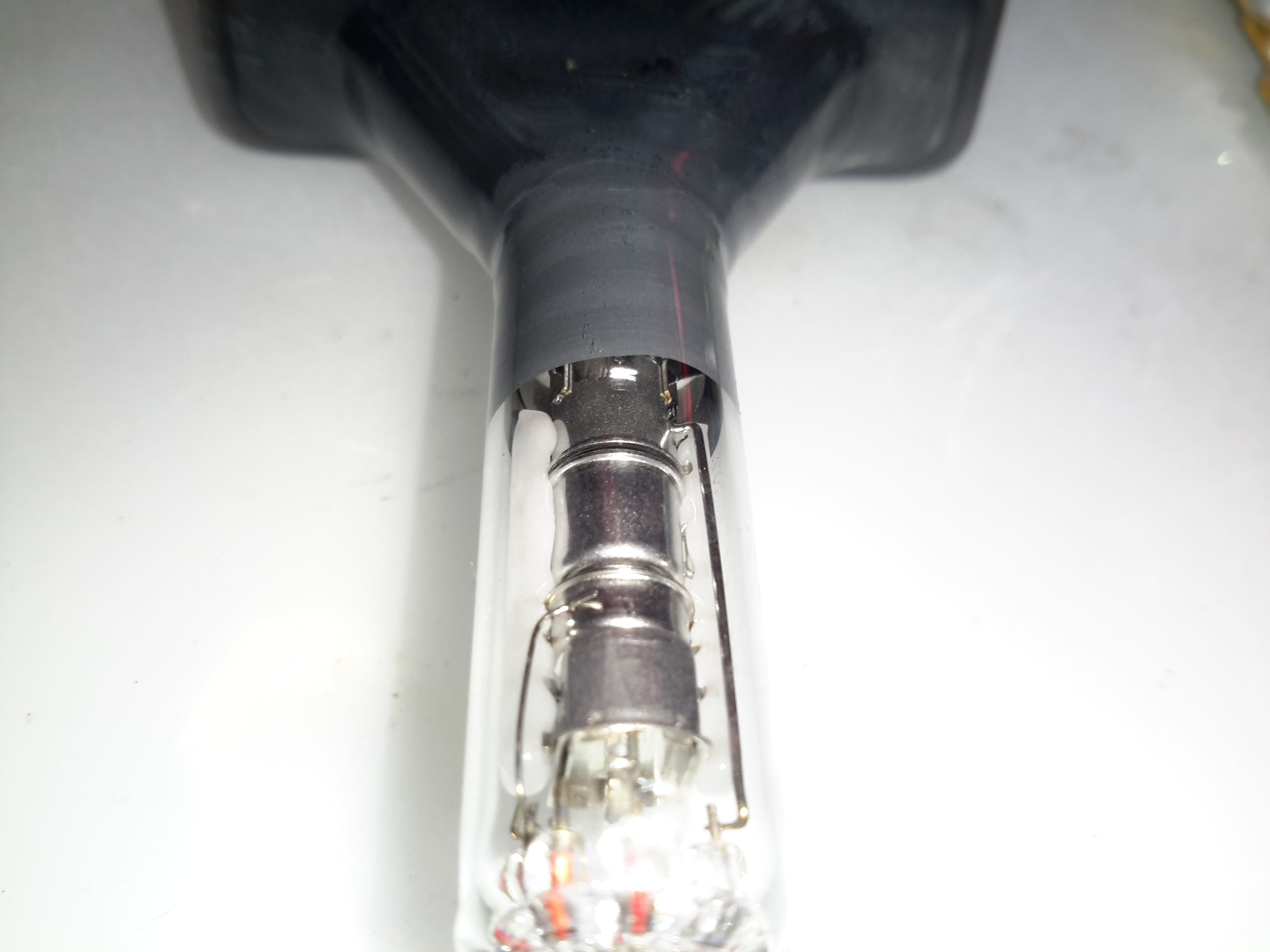
Electron Gun
Here’s the electron gun end of the tube. There isn’t a separate final anode connection to the bell of the tube unlike the previous model. Instead the final anode voltage is on a pin of the electron gun itself. This keeps all the wiring to the tube at one end & shortens the high voltage cable.
Electron Gun
Here’s the gun in the neck of the tube. Again this is pretty much standard fare for CRT guns. It’s more similar to a viewfinder tube in that the anode connection is running from the pins at the back. (It’s the line running up the right side of the tube). I’m guessing the anode voltage is pretty low for this to work without the HV flashing over, probably in the 2-4kV range.
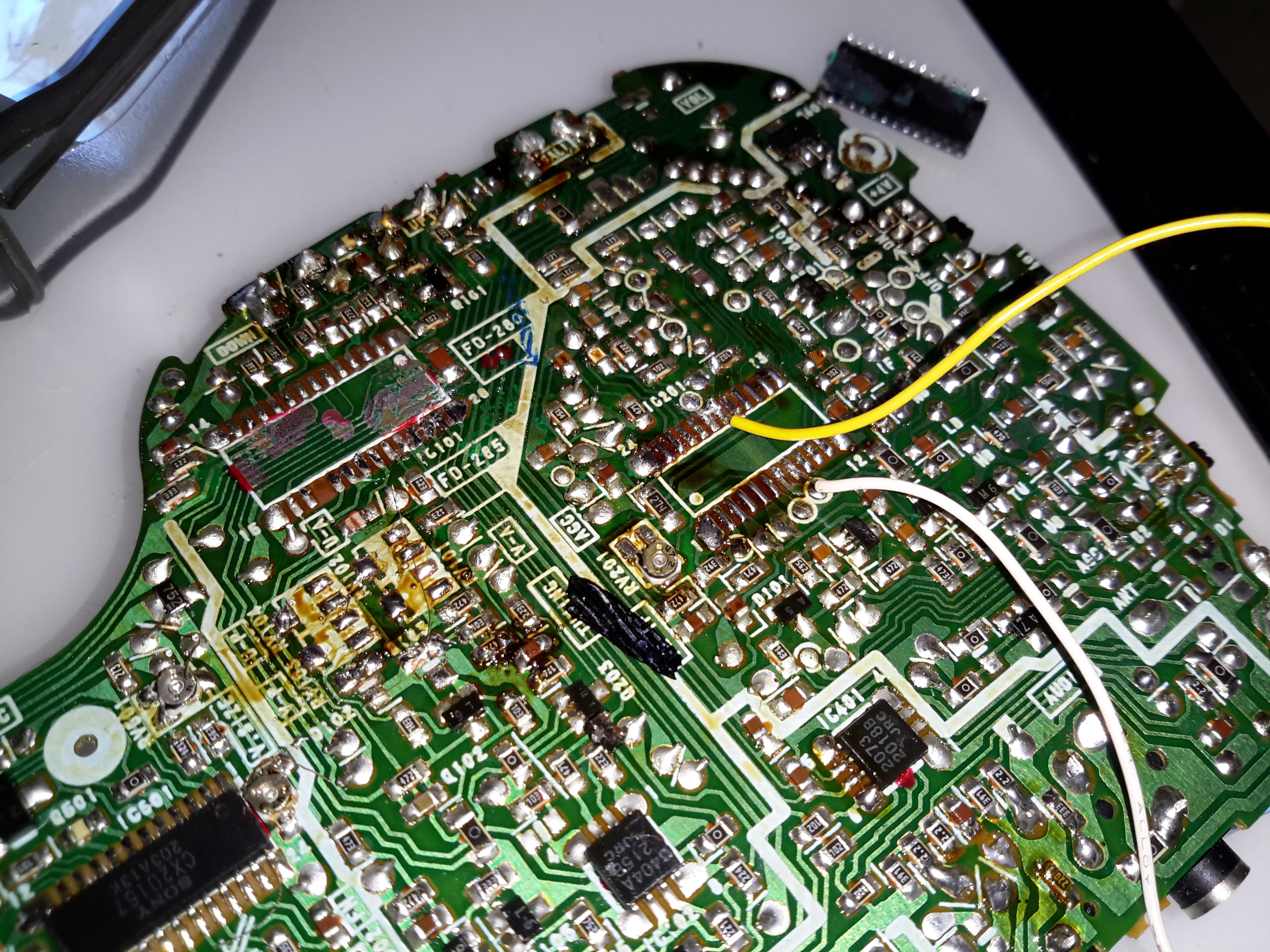
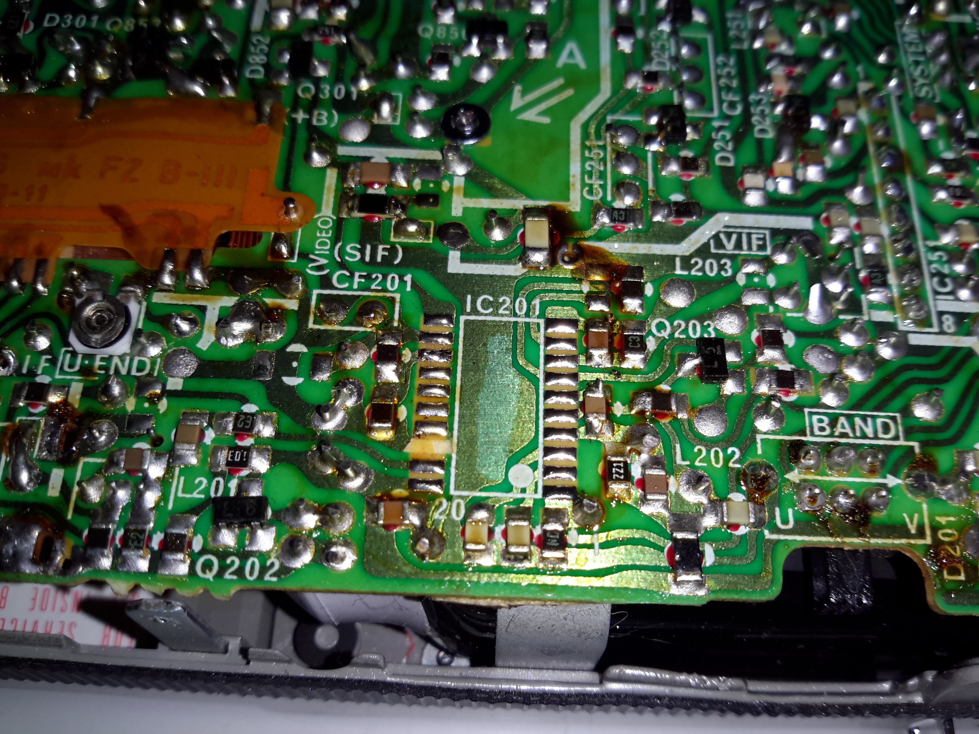
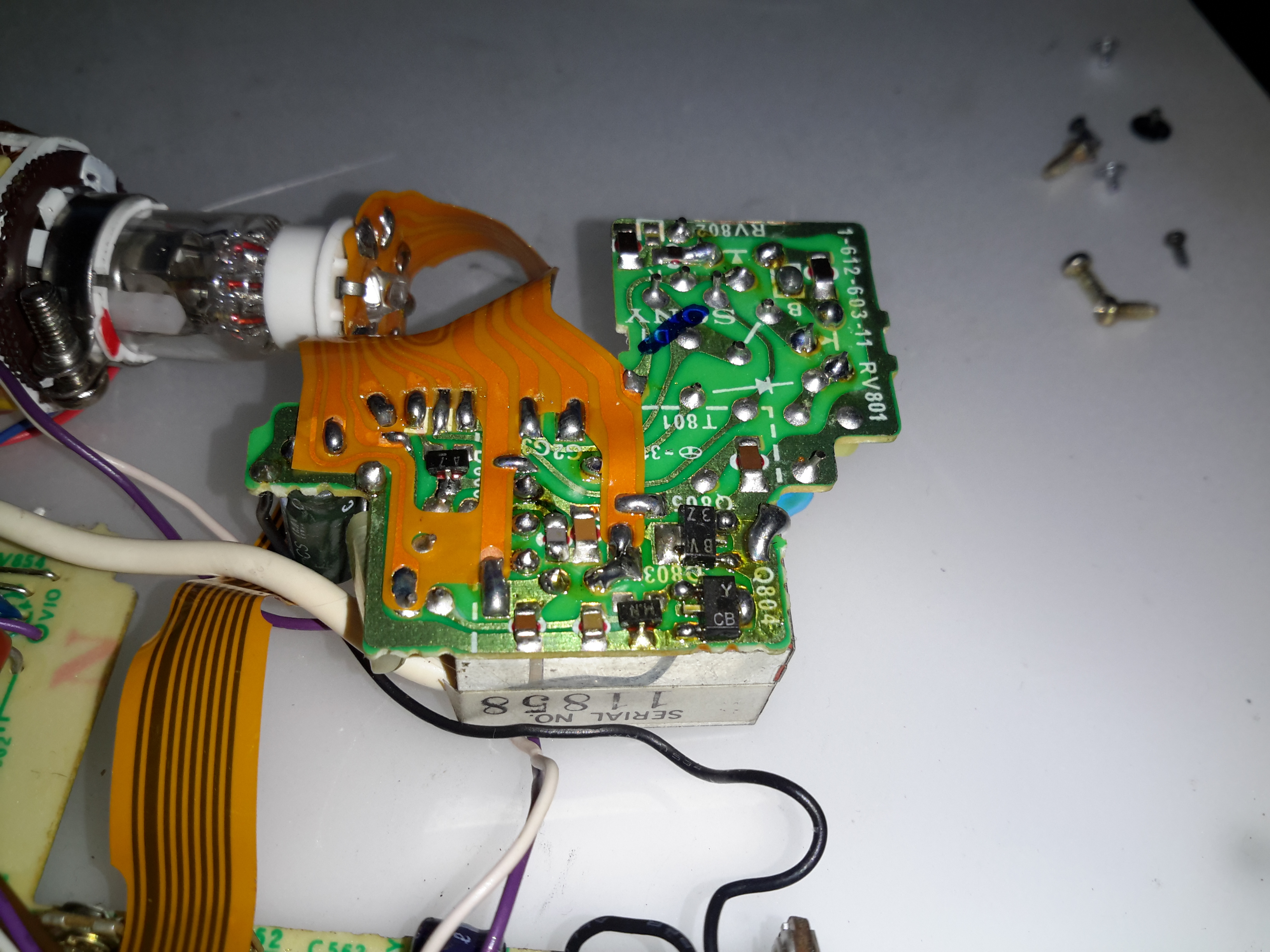
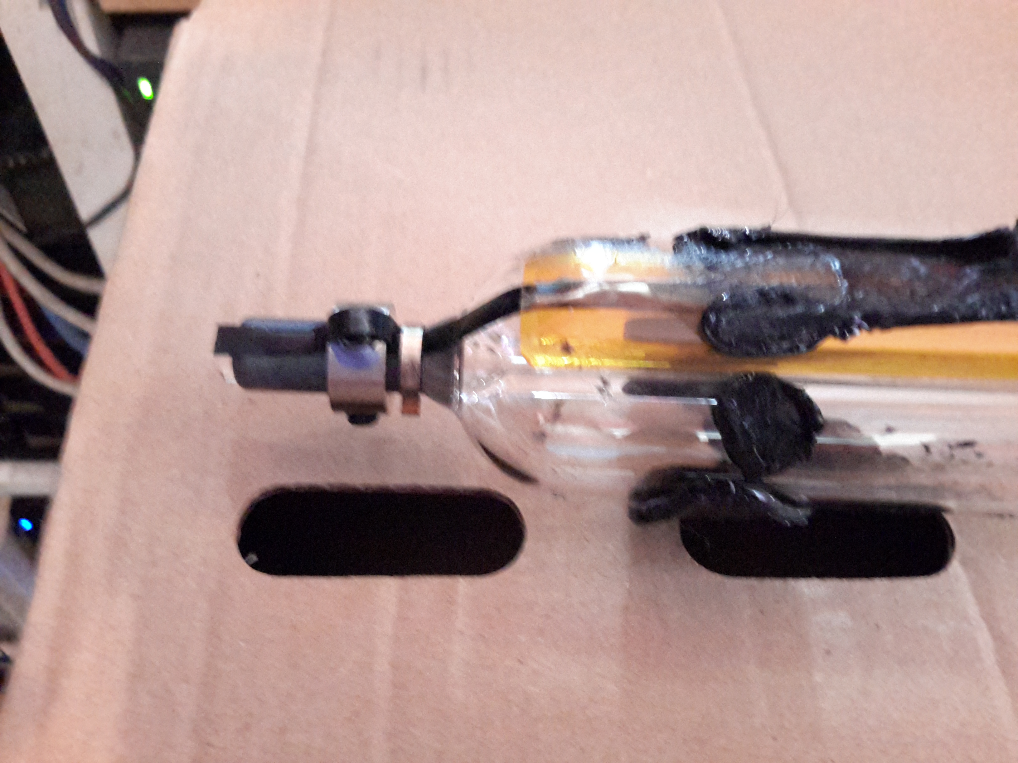
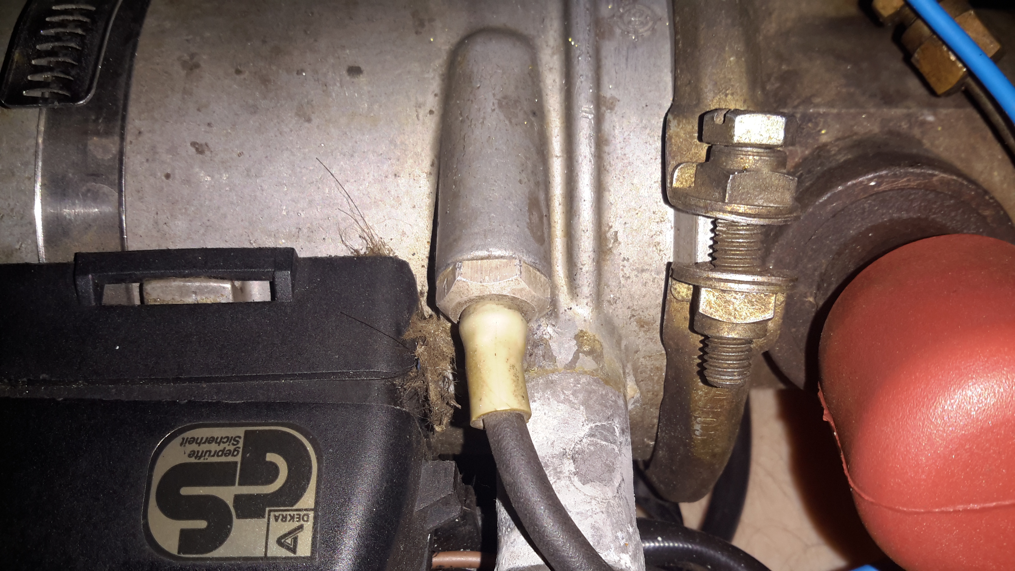
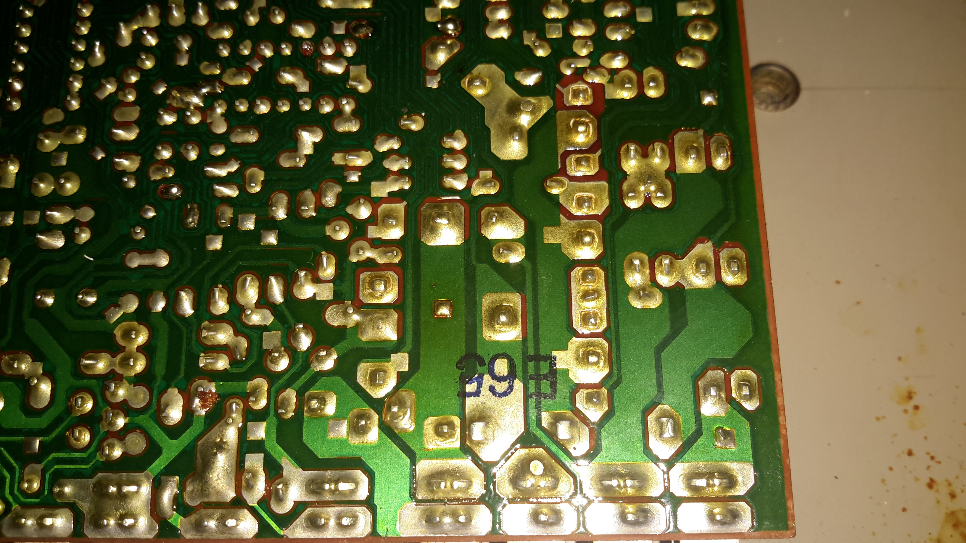
Hacking the Sony FD-20 to accept a composite input is easy – the tuner receives the RF transmission, produces an IF, this is then fed into IC201, a Mitsubishi M51364P Video IF Processor. The VIF IC then separates out the composite video signal, which is output on Pin 13 (in photo above, left side, 3rd pin from the top). The audio is separated out & sent via Pin 11 to the Audio IF processor.
In the above photo, the VIF IC has been removed from the board with hot air, as it was interfering with the signal if left in place. The RF tuner was also desoldered & removed. Unfortunately I managed to mangle a pad, which is the ground pin for the VIF IC. This isn’t much of an issue though, as an identical signal ground is available, just to the left of the IC.
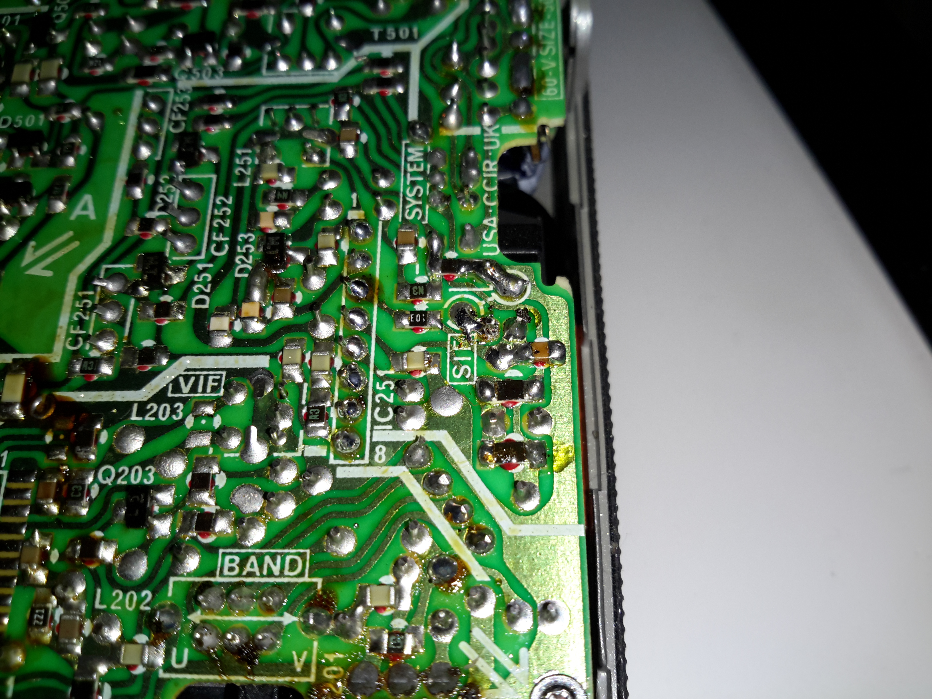
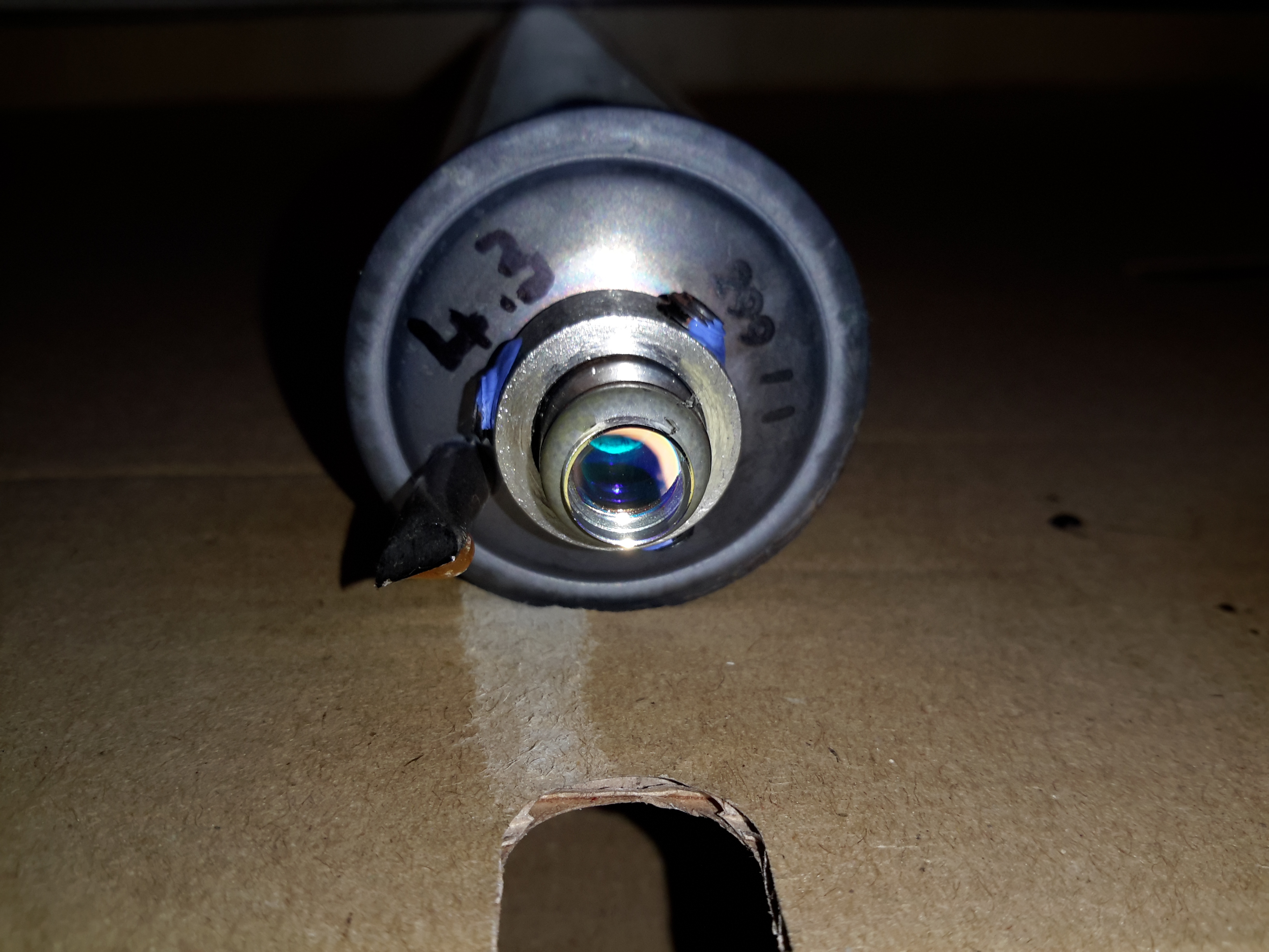
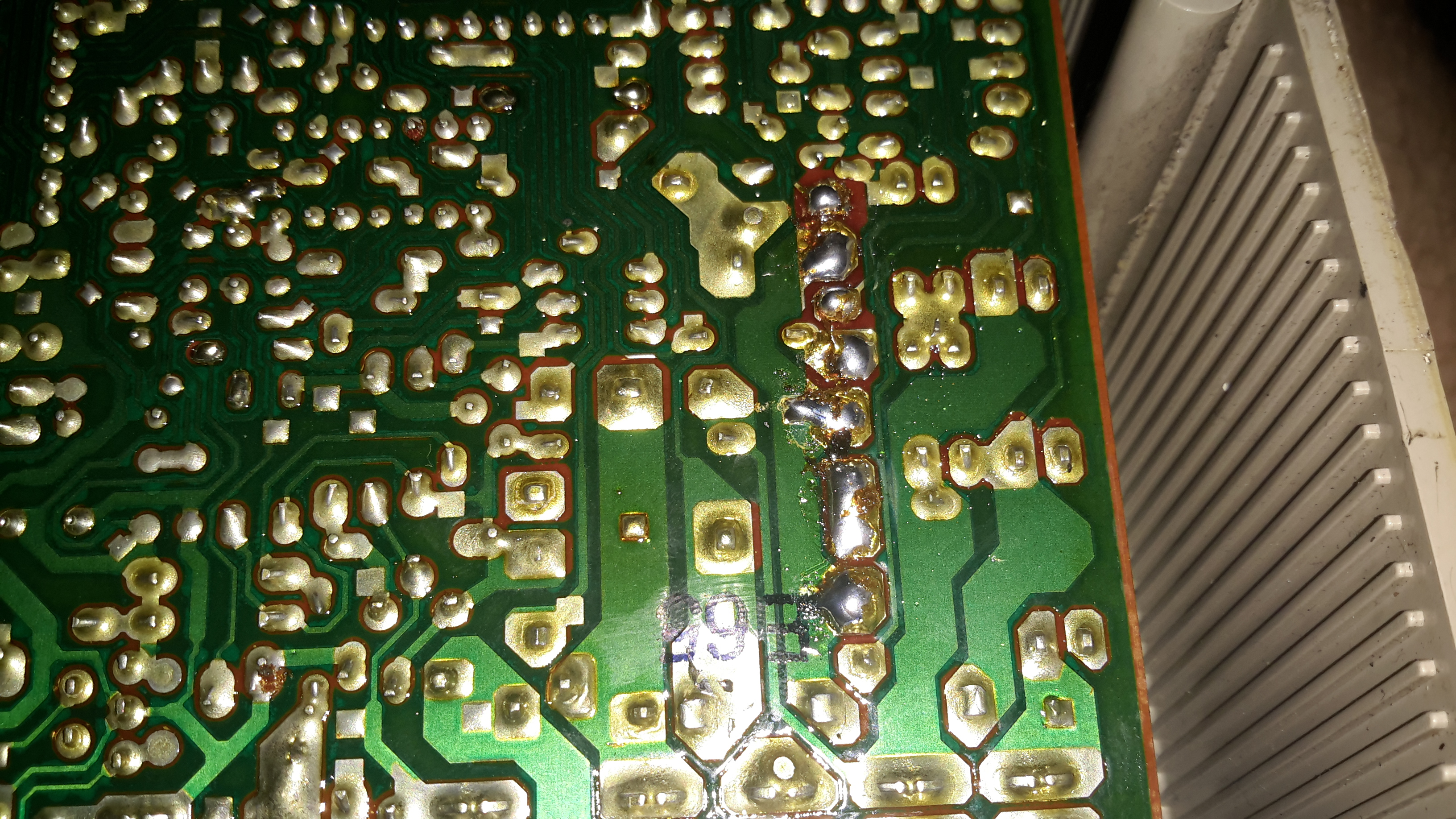
Audio Input
The audio can be tapped into in a similar way, the circled pad in the centre of the photo marked SIF is the place, this is the output of the Audio IF processor to the audio amplifier. The Audio IF processor didn’t interfere with the injected signal, so it was left in place.
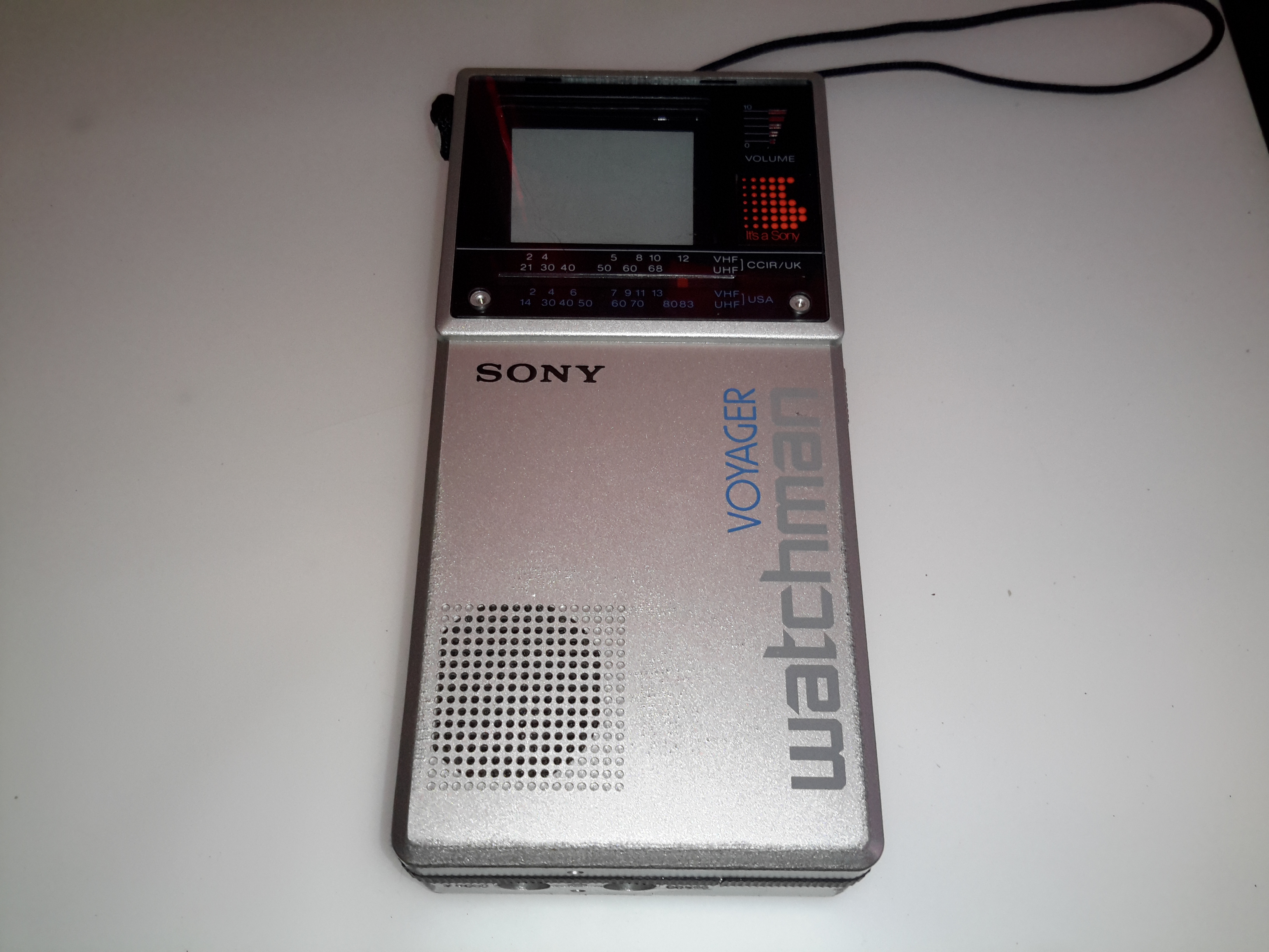
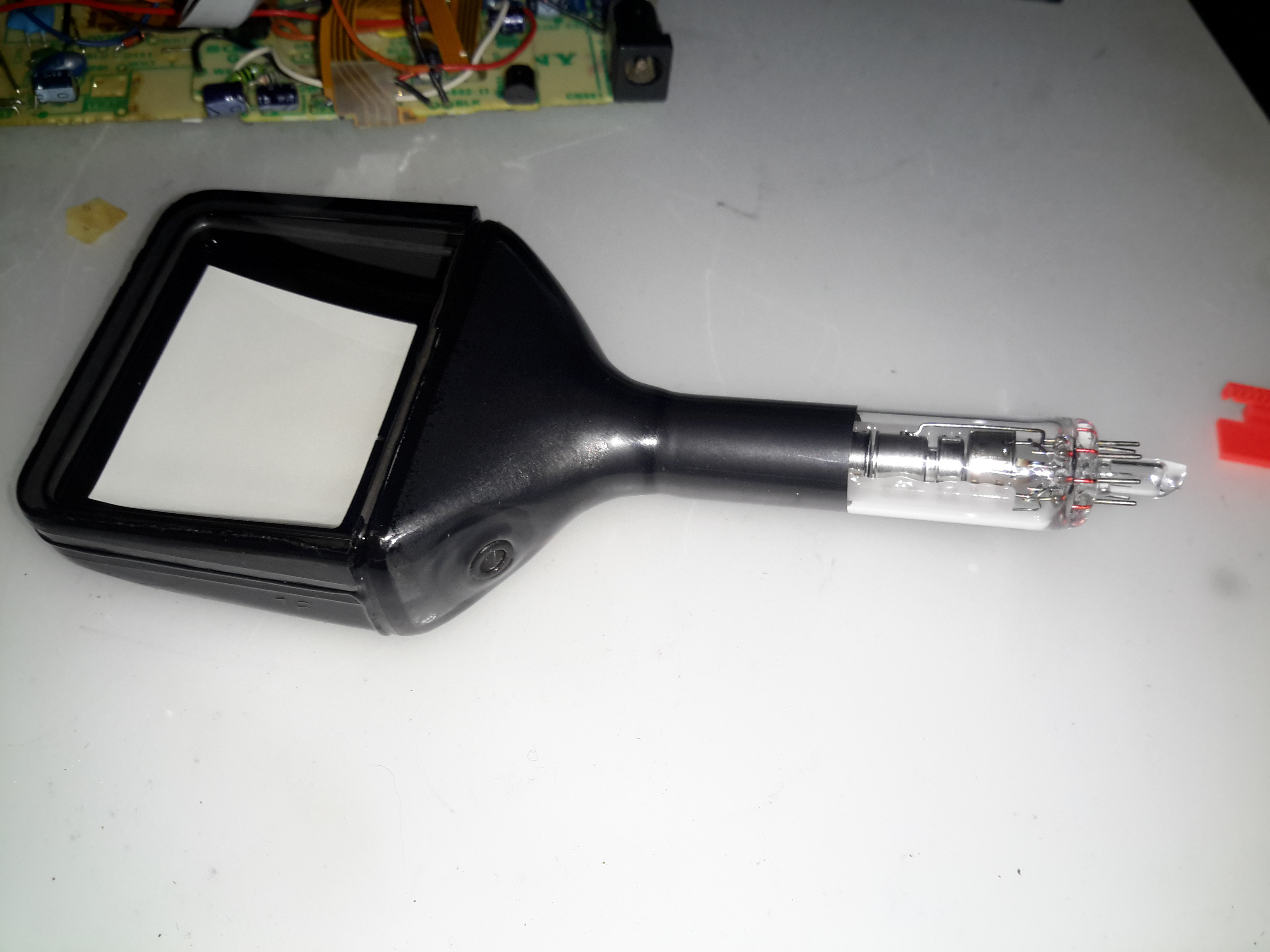
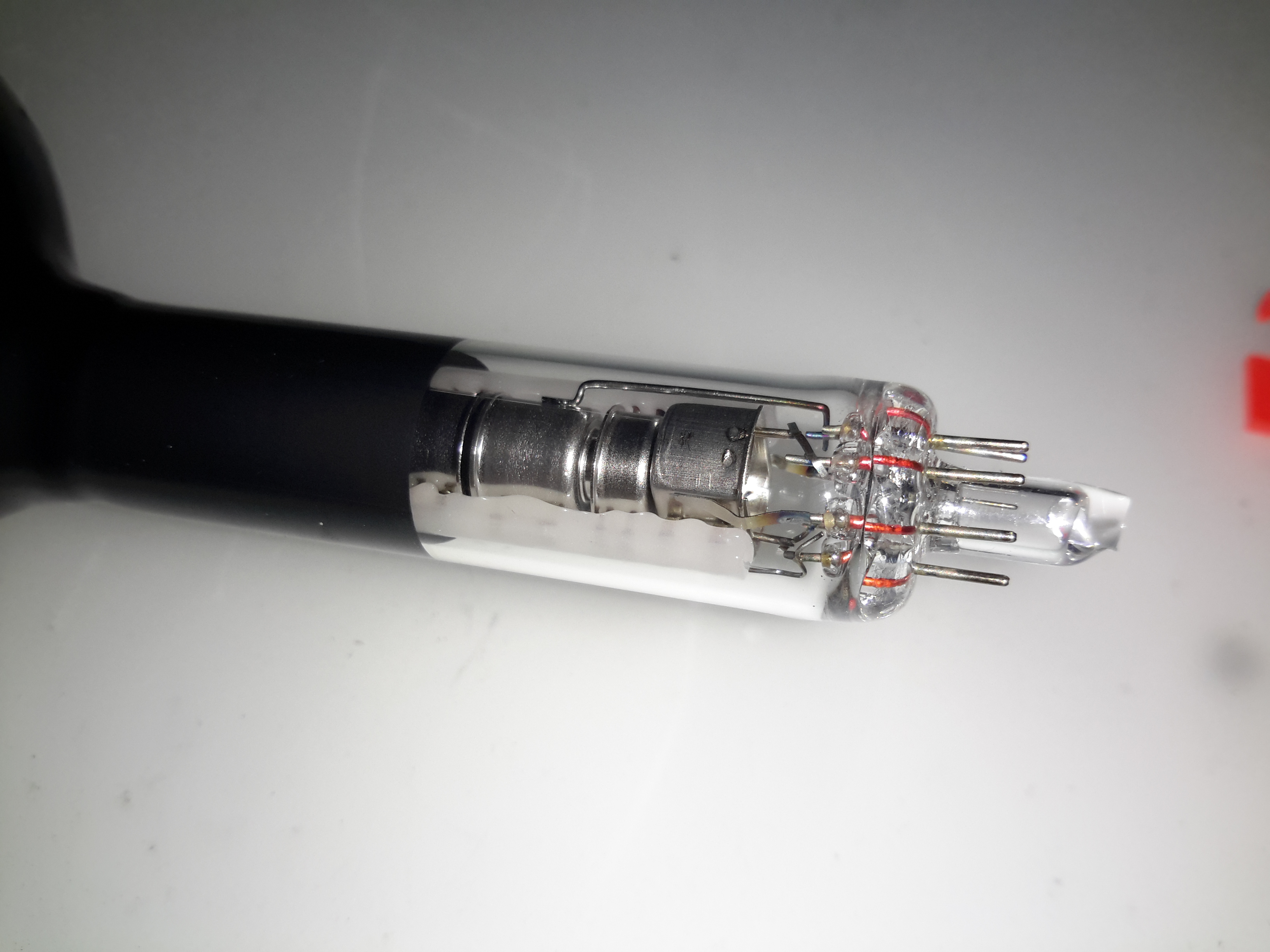
Here’s an oddity from the 1980’s – a CRT-based portable TV, with a very strangely shaped tube. Sony produced many types of flat CRTs back in the 80’s, with the electron gun at 90° to the curved phosphor screen.
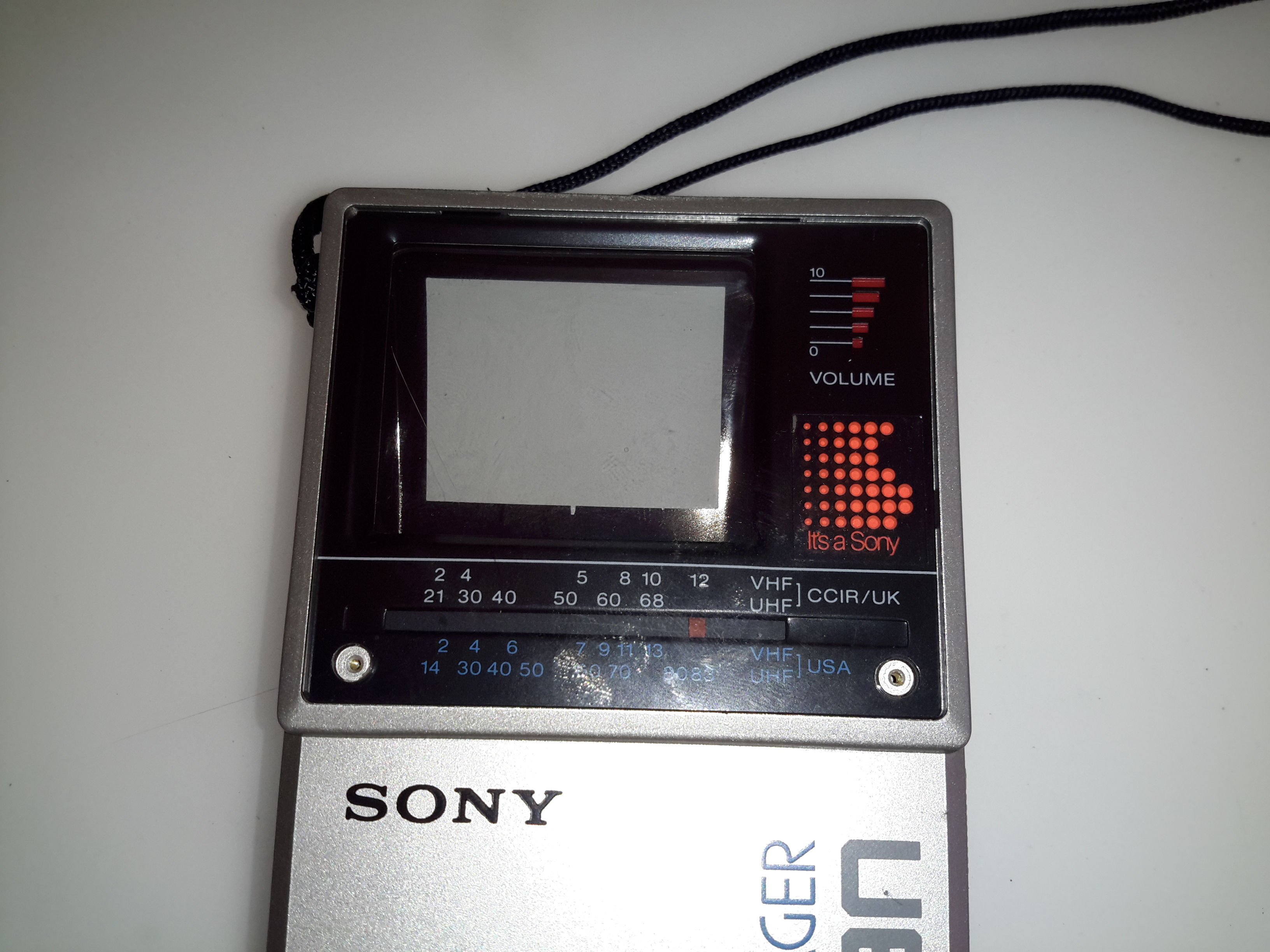
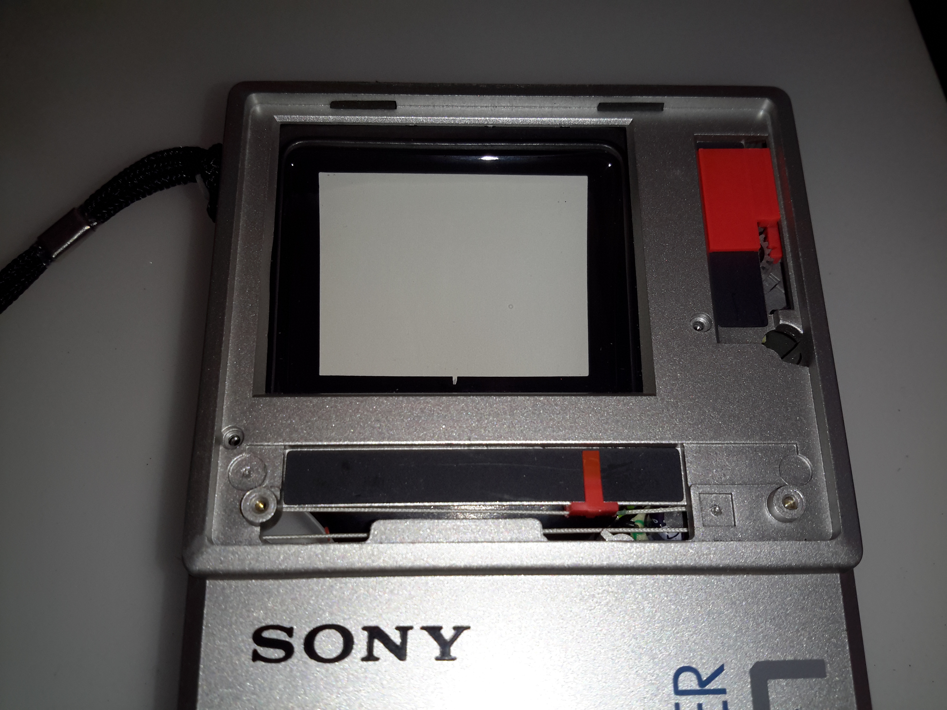
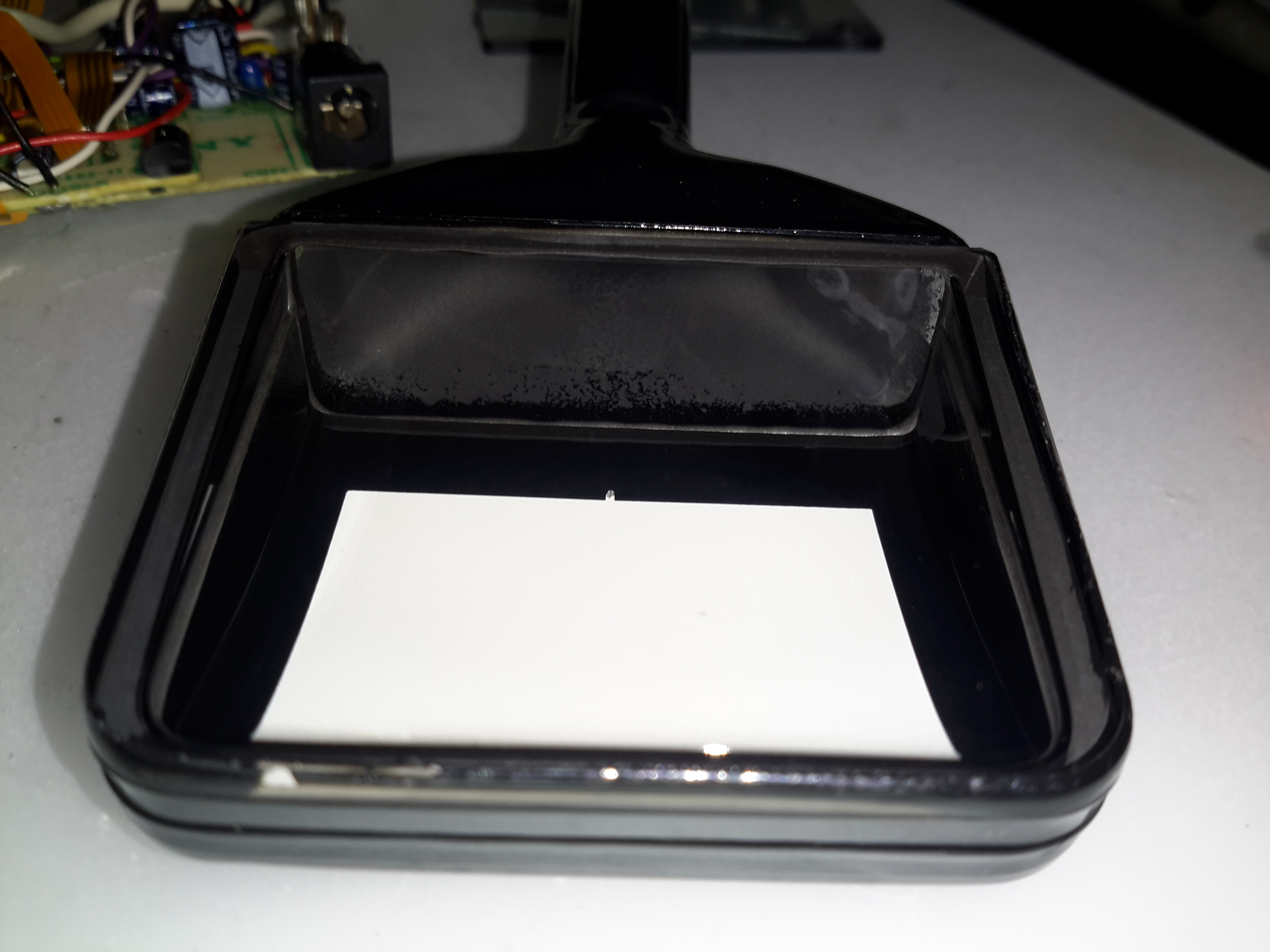
Front Panel
The front panel has the display window, along with the tuning & volume indicators. Unfortunately since analogue TV transmissions have long been switched off, this unit no longer picks up any transmissions off the air, but it can be modified to accept a composite video input.
Back Panel
The back panel has the battery compartment & the tilt stand.
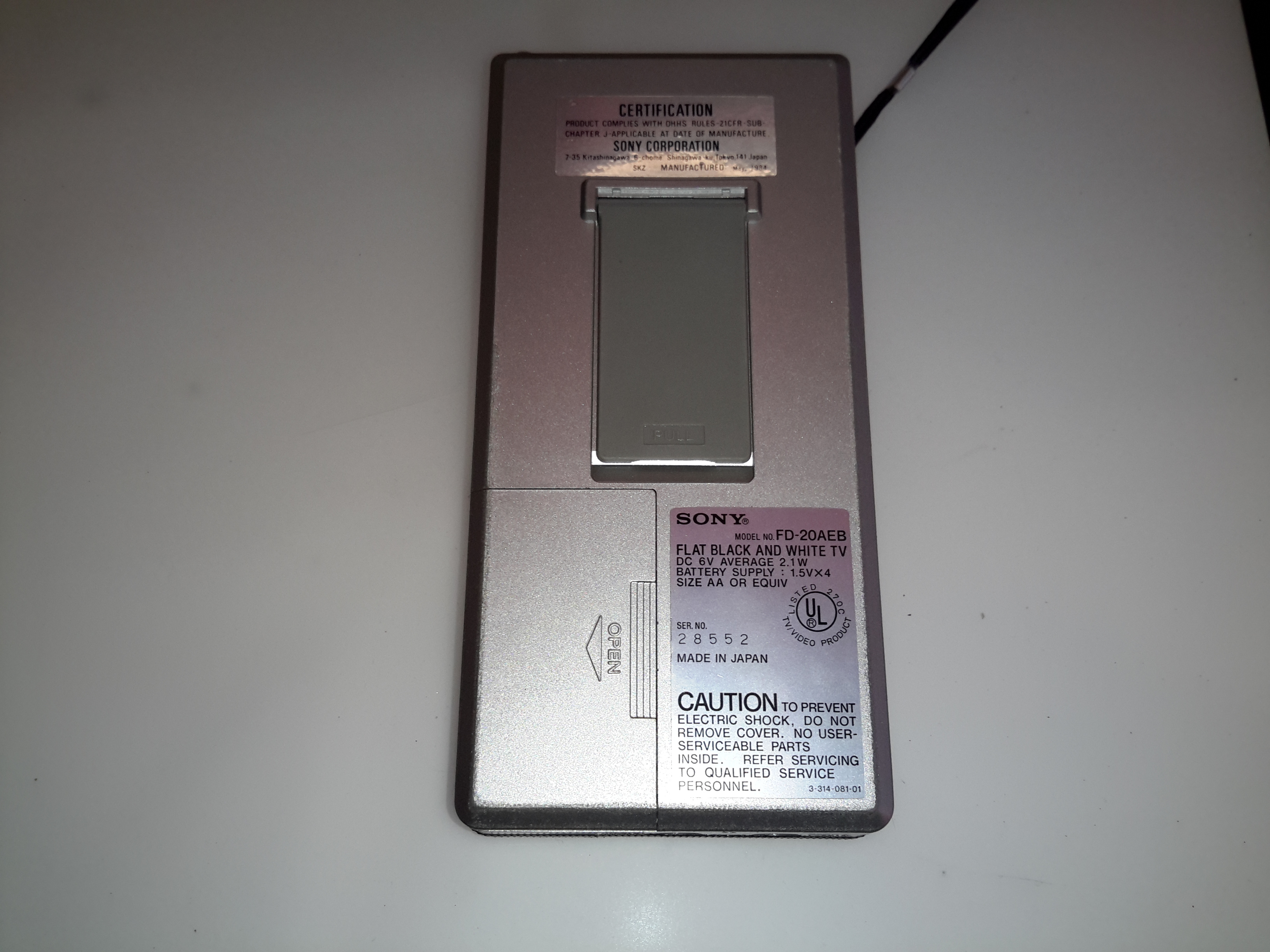
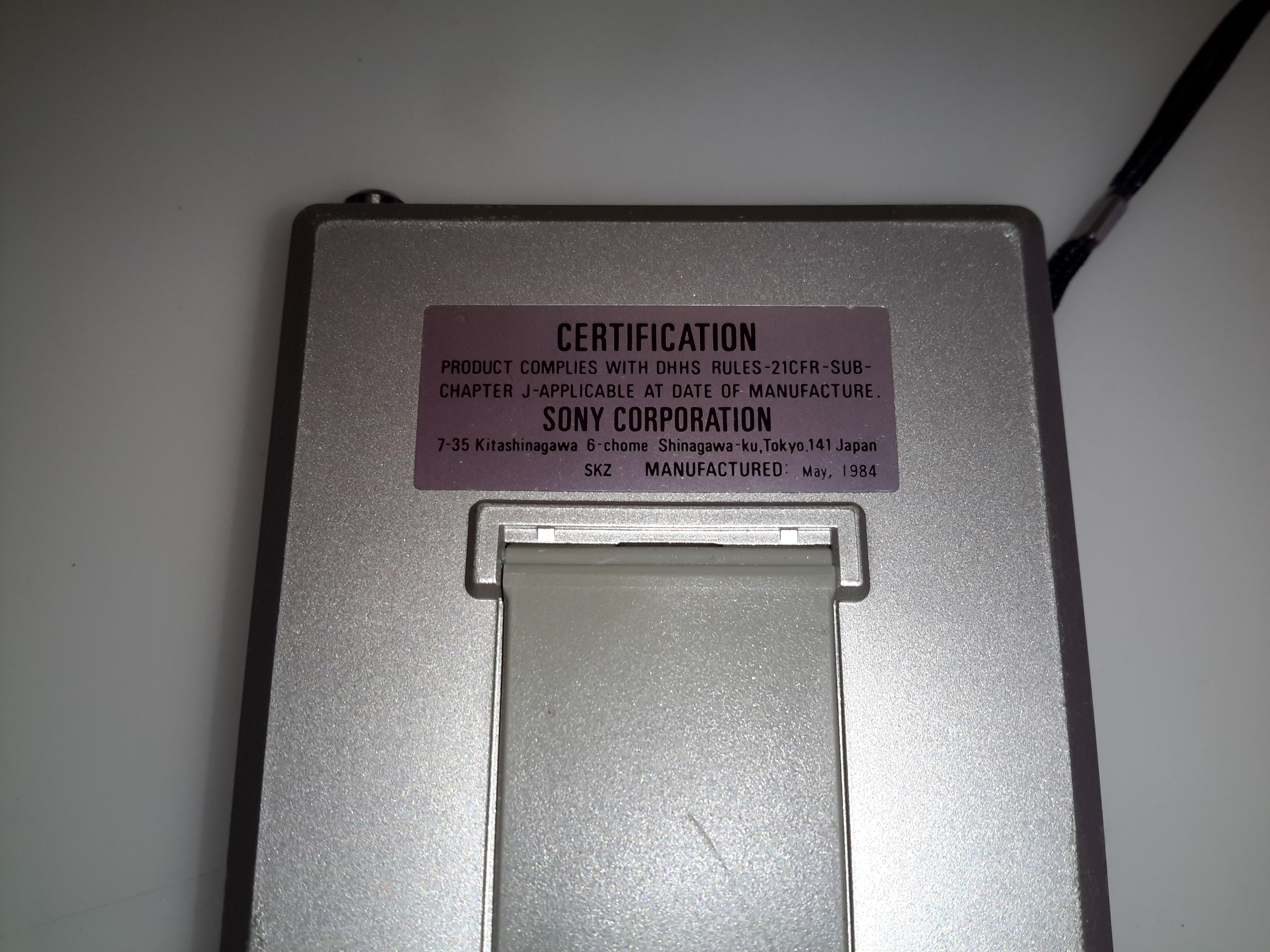
Certification
The certification label reveals this unit was manufactured in May 1984, 32 years ago!
Spec. Label
Rated at 6v, ~2.1W this device uses surprisingly little power for something CRT based.
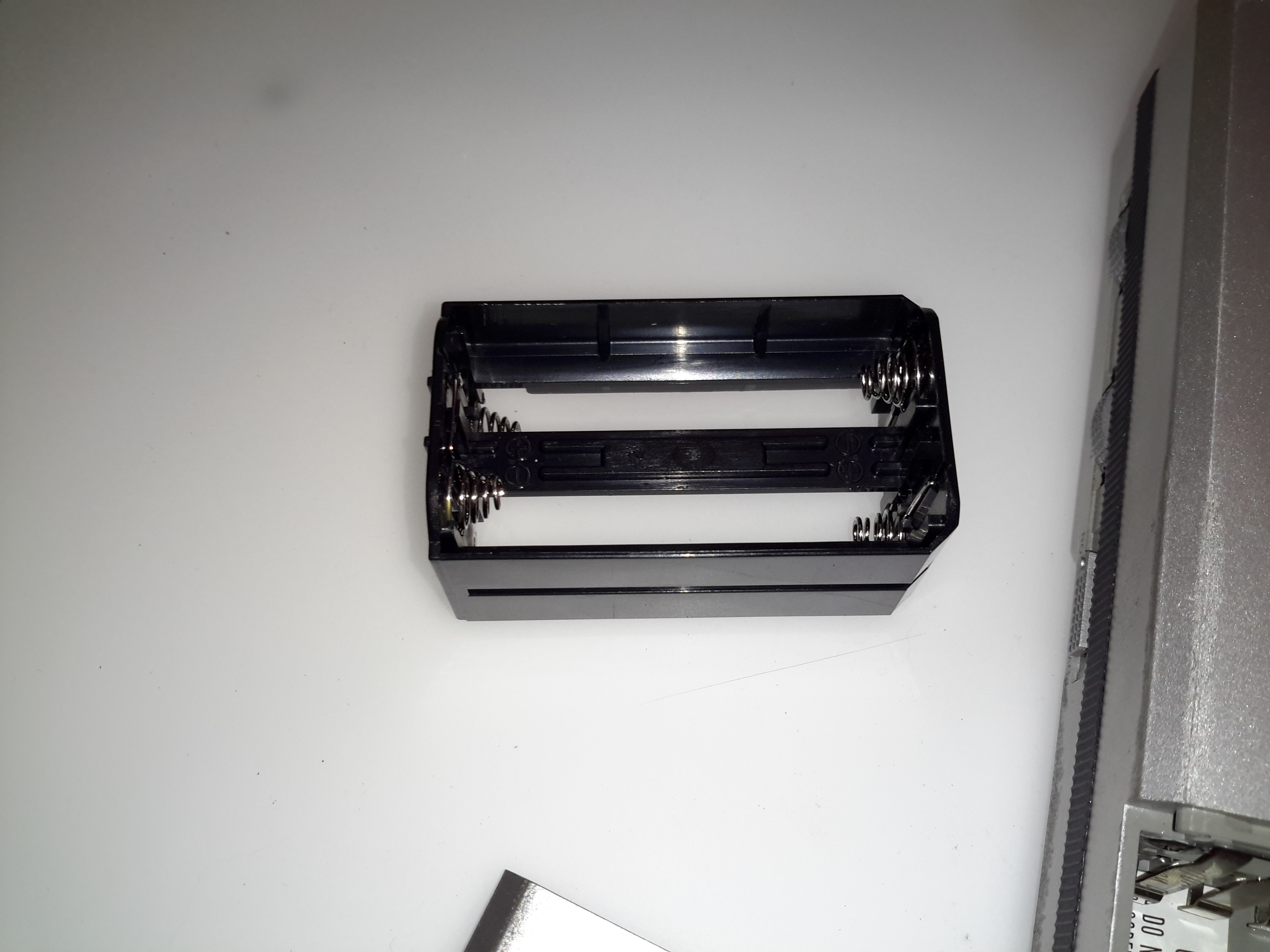
Battery Holder
The battery holder is a little unique, this plastic frame holds 4 AA cells, for a 6v pack.
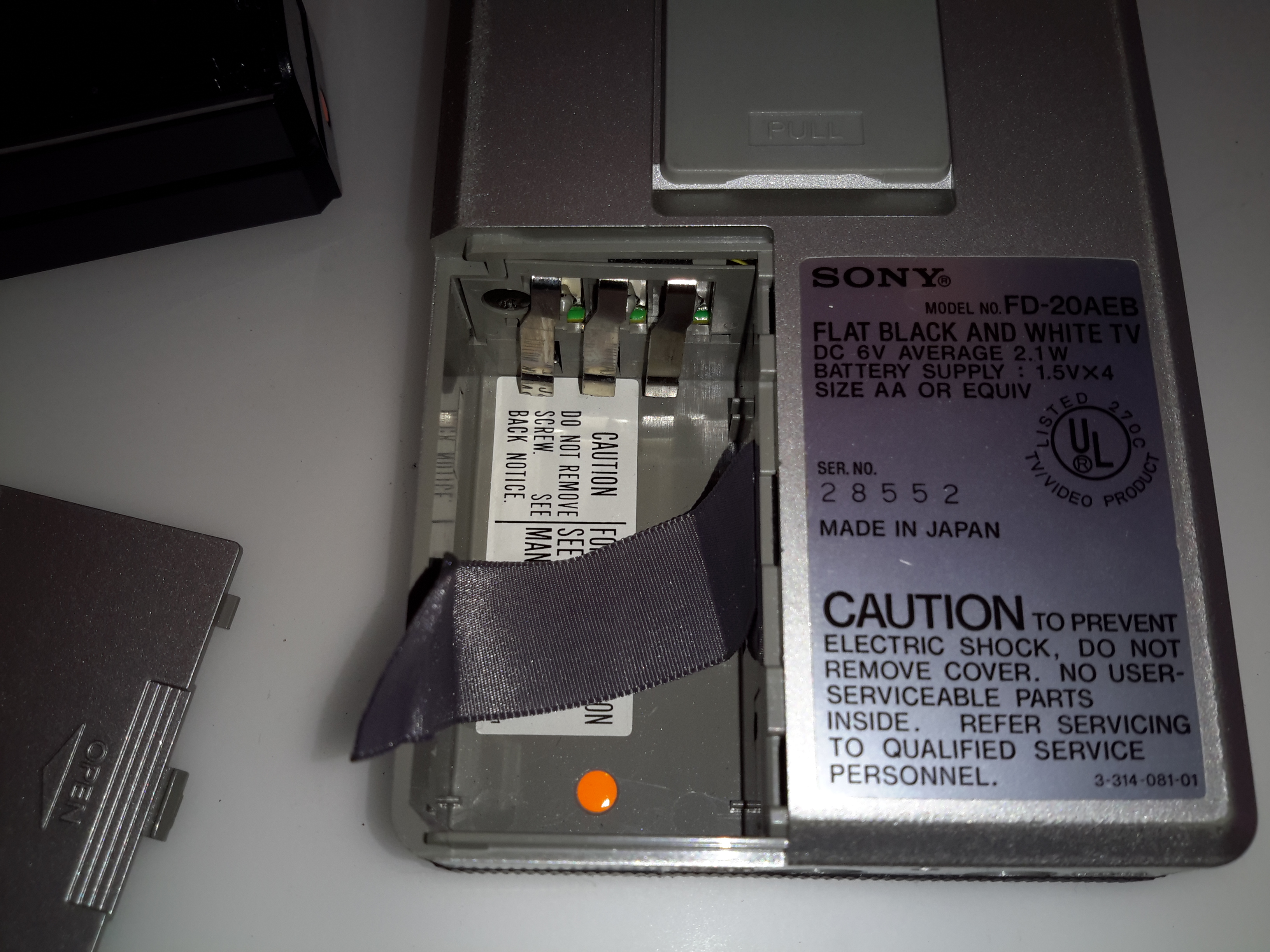
Battery Compartment
The battery holder slots into the back of the TV, there’s also an extra contact that the service manual mentions is for charging, so I assume a rechargeable 6v battery pack was also available.
Front Panel Removed
Removing a pair of pin-spanner type screws allows the front glass & screen printed CRT surround to be removed. Not much more under here other than the pair of screws that retain the CRT in the front frame.
Back Cover Removed
Here’s the back cover removed, after unscrewing some very small screws. As per usual with Sony gear, the electronics is extremely compacted, using many flat flex cables between the various PCBs. The main PCB is visible at the back, this has all the deflection circuitry, RF tuner, Video IF, Audio IF, video amplifier & composite circuitry.
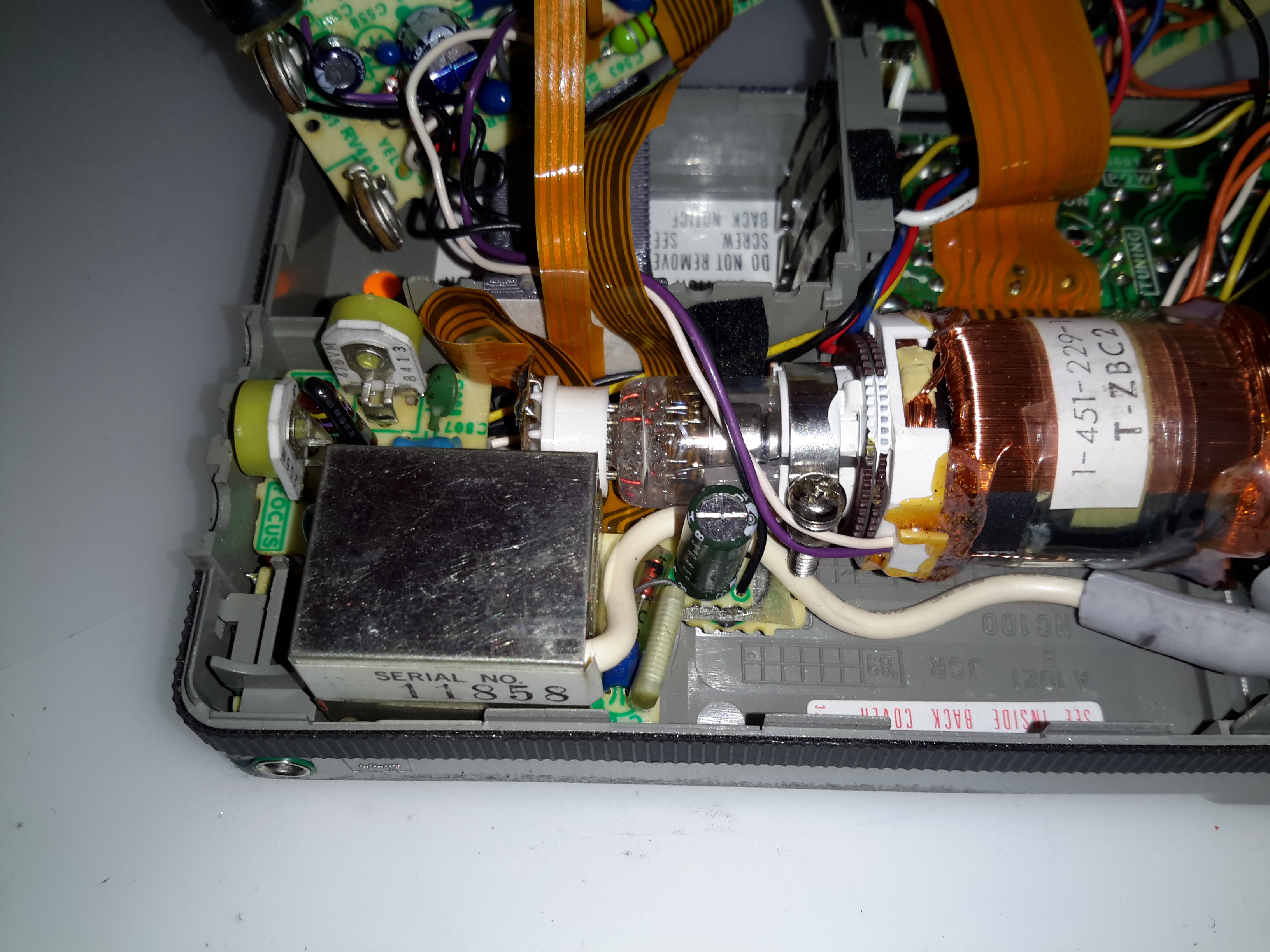
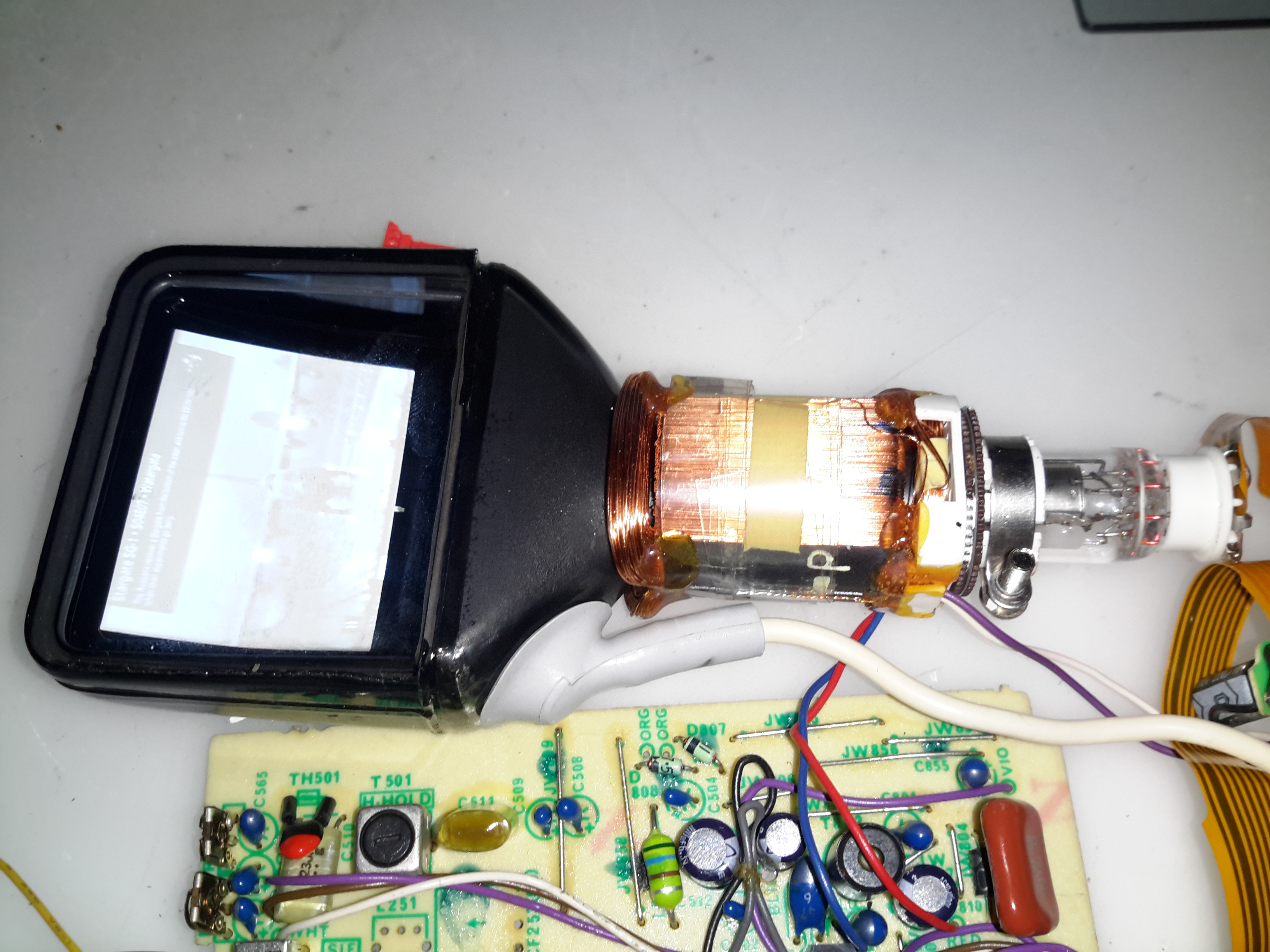
CRT Electron Gun & Flyback Transformer
Lifting up the main board reveals more PCBs – the high voltage section for the CRT with the flyback transformer, focus & brightness controls is on the left. The loudspeaker PCB is below this. The CRT electron gun is tucked in behind the flyback transformer, it’s socket being connected to the rest of the circuitry with a flat flex cable.
CRT Rear
Here’s the back of the CRT, the phosphor screen is on the other side of the curved glass back. These tubes must require some additional deflection complexity, as the geometry will change as the beam scans across the screen. There’s a dynamic focus circuit on the schematics, along with extensive keystone adjustments.
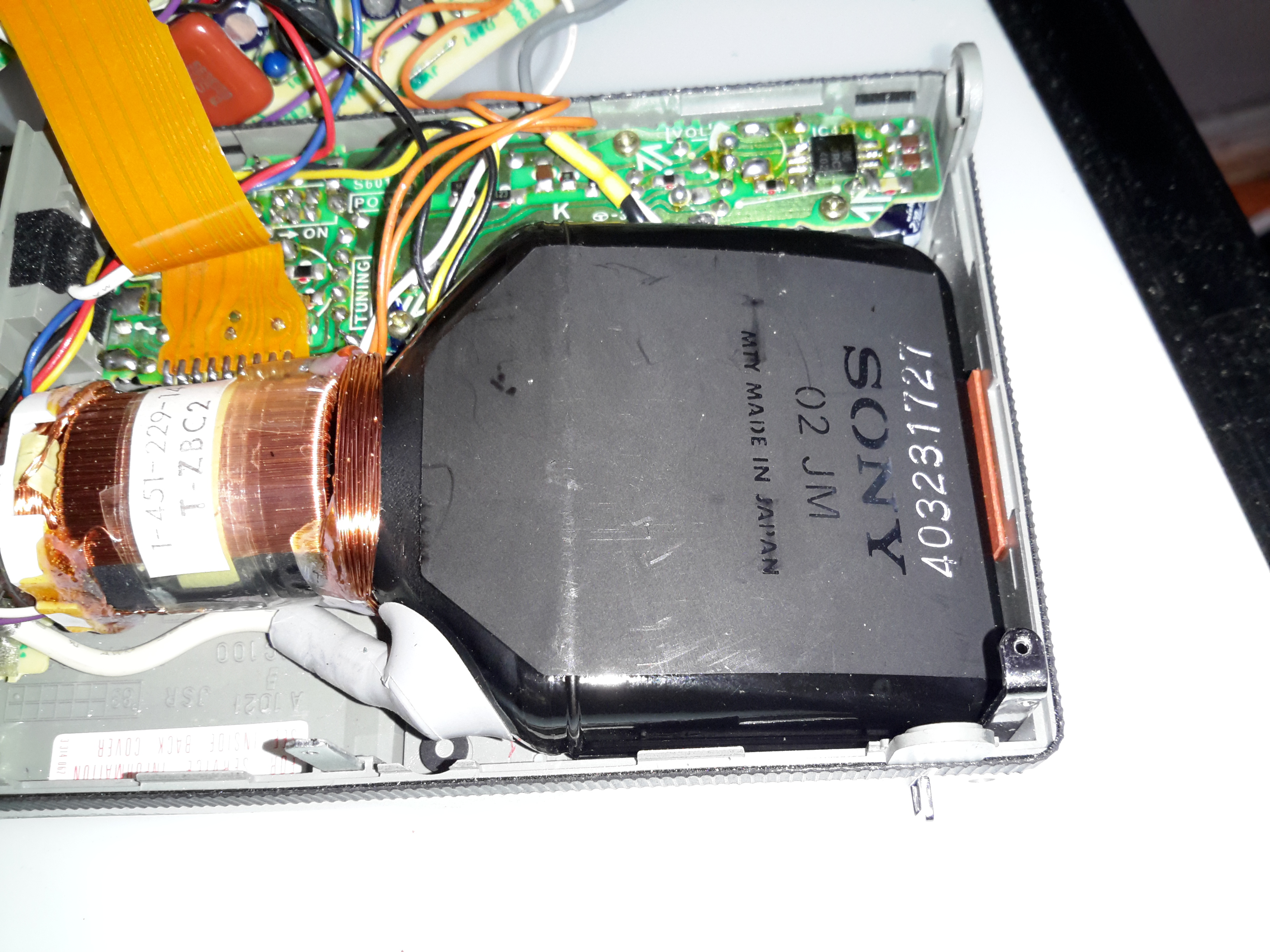
Sony 02-JM Flat CRT
Here’s the tube entirely extracted from the chassis. The EHT connection to the final anode is on the side of the tube bell, the curved phosphor screen is clearly visible. The one thing I can’t find in this CRT is a getter spot, so Sony may have a way of getting a pure enough vacuum that one isn’t required.
I’d expect the vertical deflection waveforms to be vastly different on this kind of CRT, due to the strange screen setup. Not much of a beam movement is required to move the spot from the top to the bottom of the screen.
HV Module
No doubt to keep the isolation gaps large, all the high voltages are kept on a separate small PCB with the flyback transformer. This board generates the voltages for the electron gun filament, focus grid & the bias to set the beam current (brightness) as well.
Bare CRT
Here the deflection yoke has been removed from the CRT, showing the very odd shape better. These tubes are constructed of 3 pieces of glass, the bell with electron gun, back glass with phosphor screen & front viewing window glass. All these components are joined with glass frit.
Electron Gun
The electron gun in the neck looks to be pretty much standard, with all the usual electrodes.
Viewing Window
Here’s a view from the very top of the CRT, the curve in the screen is very obvious here. The electron beam emerges from the bell at the back.
FD-20 Schematic
Here’s the full schematic of the entire TV, I extracted this from a service manual I managed to find online.
More to come on hacking this unit to accept a standard composite video input, from something such as a Raspberry Pi!
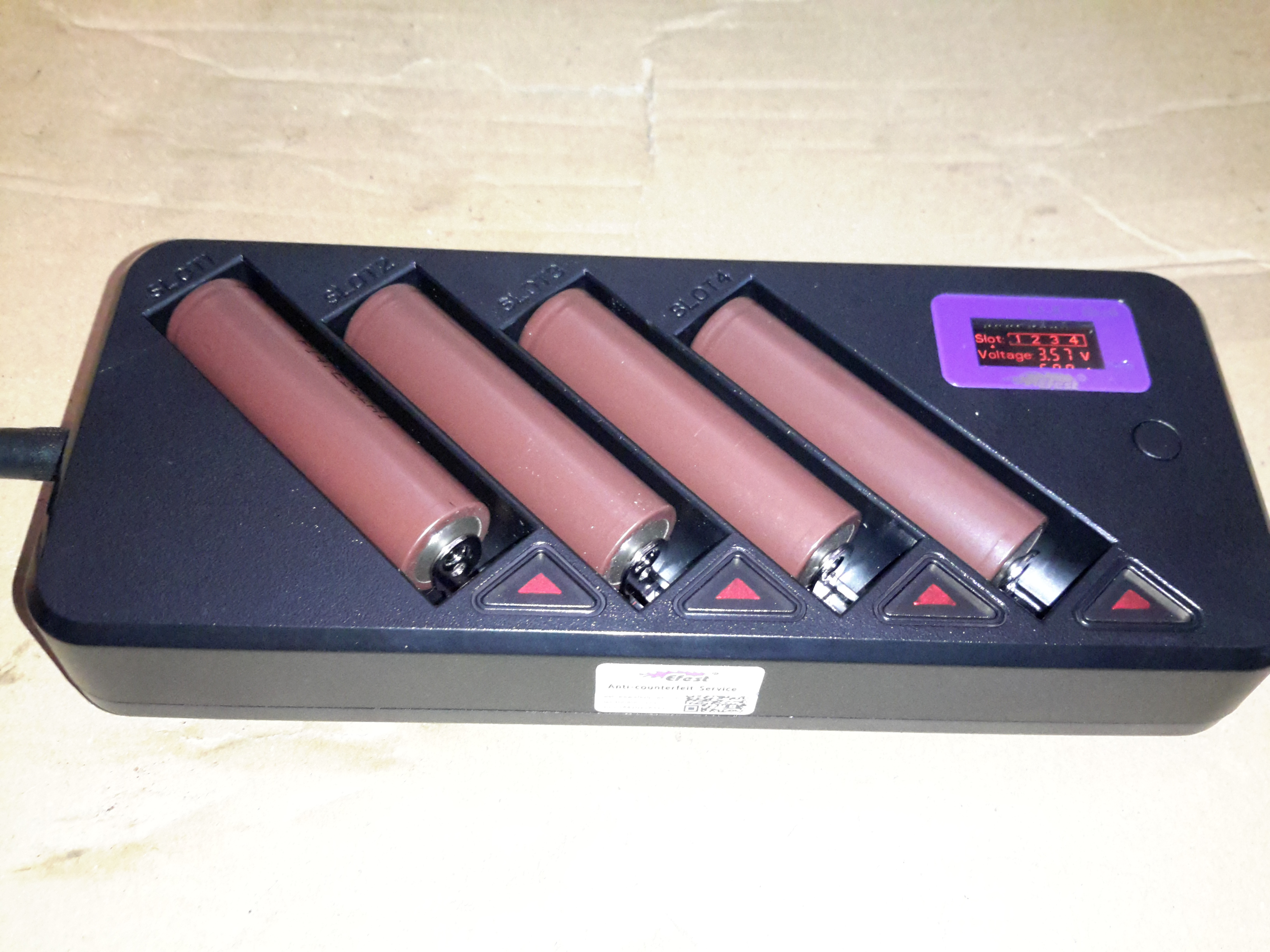
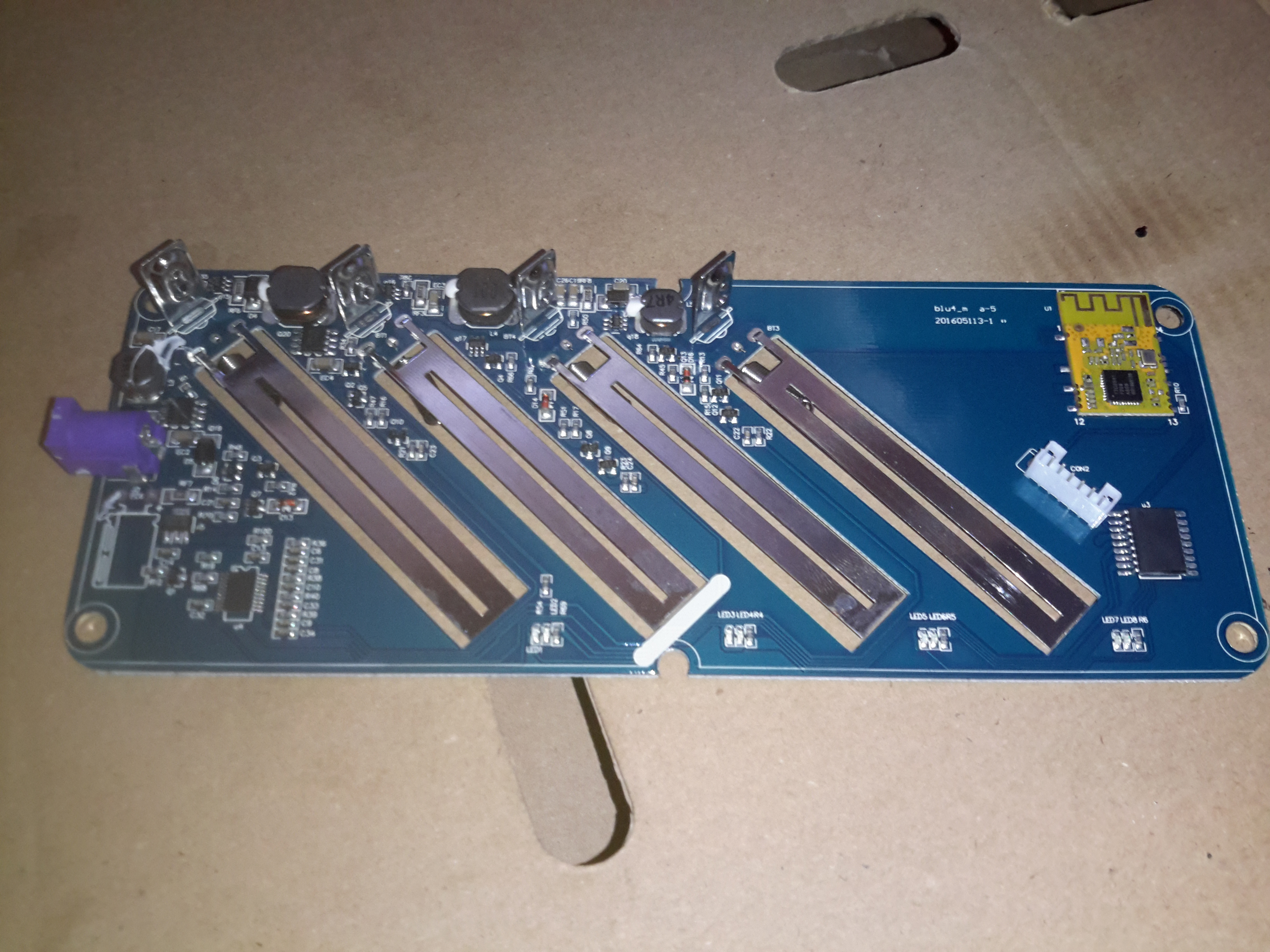
Here’s another battery charger designed for lithium chemistry cells, the BLU4. This charger doesn’t display much on it’s built in LCD, apart from basic cell voltage & charging current limits, as it has a built in Bluetooth module that will link into an Android or iOS app.
Above the charger is operating with 4 brand new cells, at a current of 500mA per cell. If only a pair of cells is being charged, the current can be increased to 1A per cell.
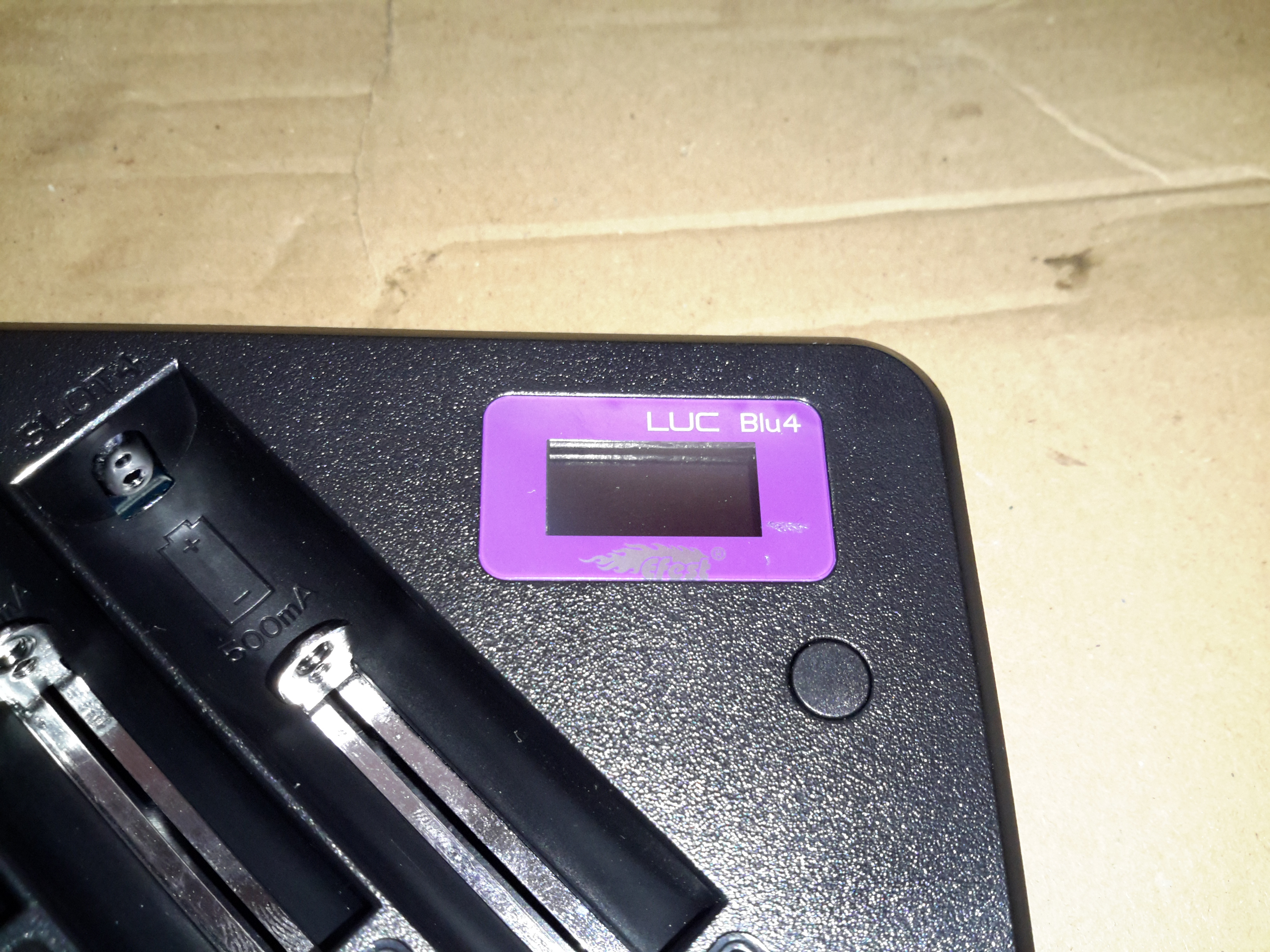
LCD
Not much in the way of user interface on the charger, a tiny LCD & single button for cycling through the display options.
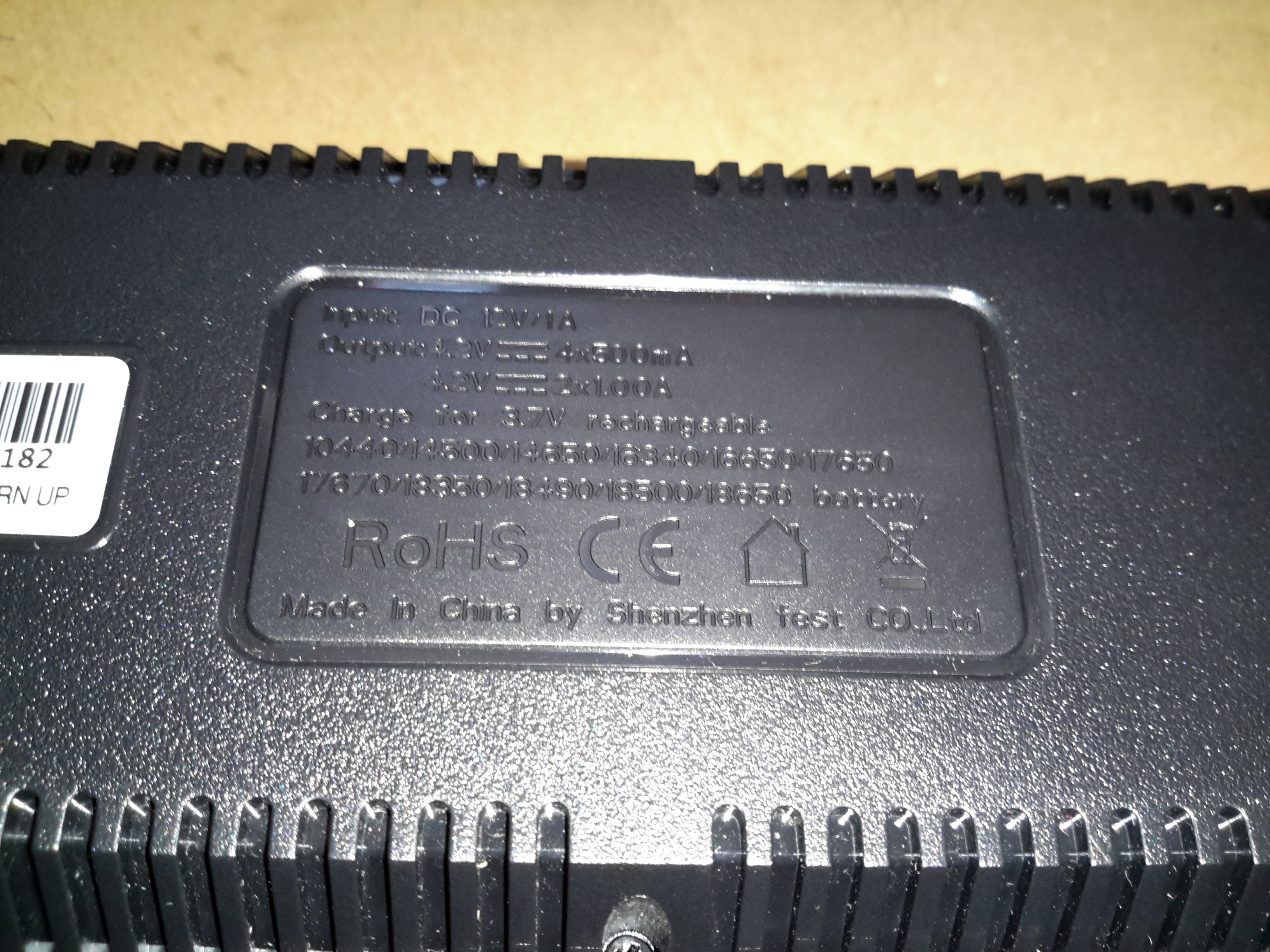
Dataplate
The usual stuff on the data plate, the charger accepts an input of 12v DC at 1A.
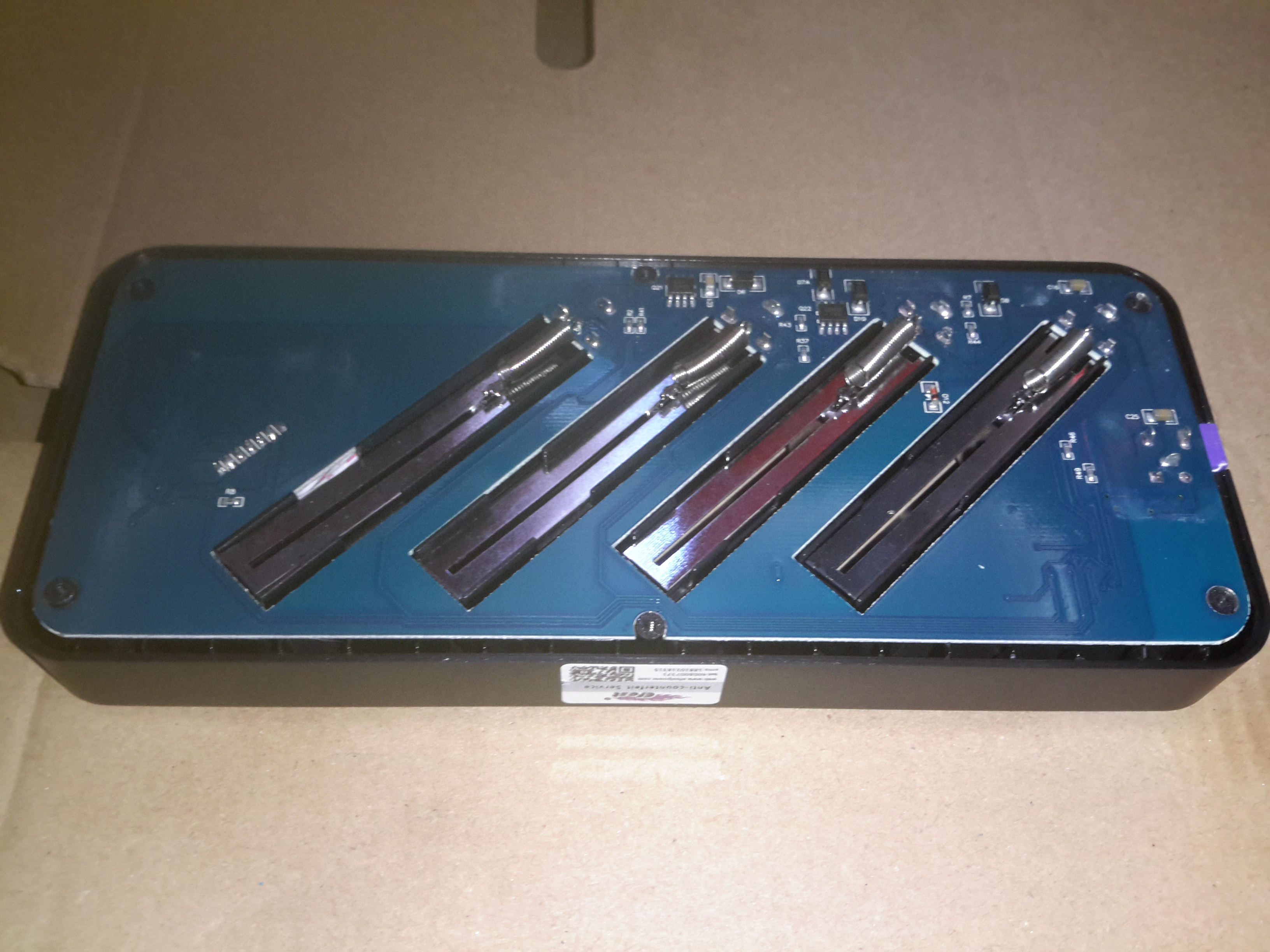
Bottom Cover Removed
Removing the 6 screws on the bottom of the casing allows the board to be seen. Not much on the bottom, the 4 cell negative connections can be seen, with their springs for adjusting for cell length.
MOSFETs
There’s a couple of P-Channel FETs on the bottom side for the charging circuits, along with some diodes.
Main PCB
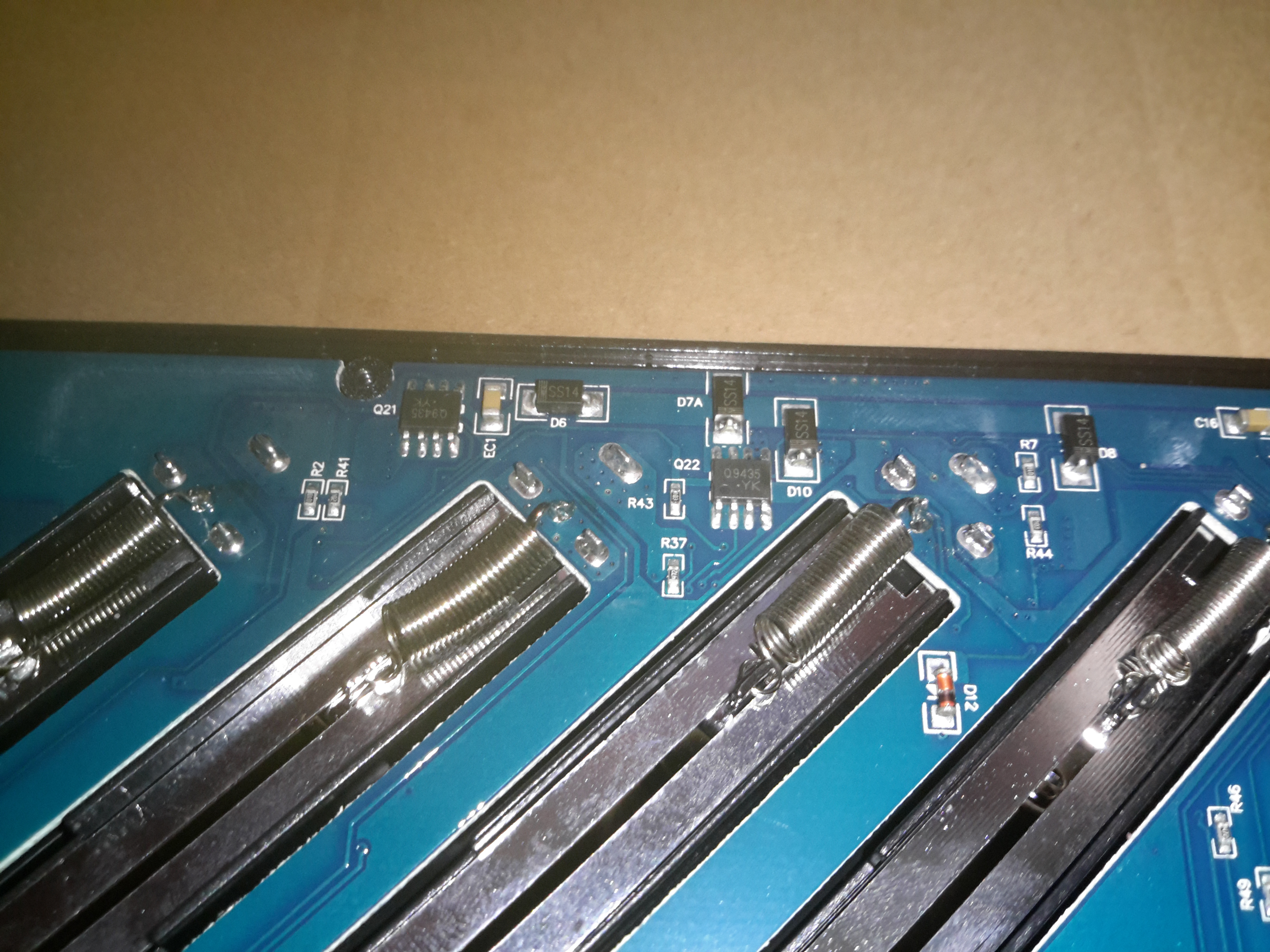
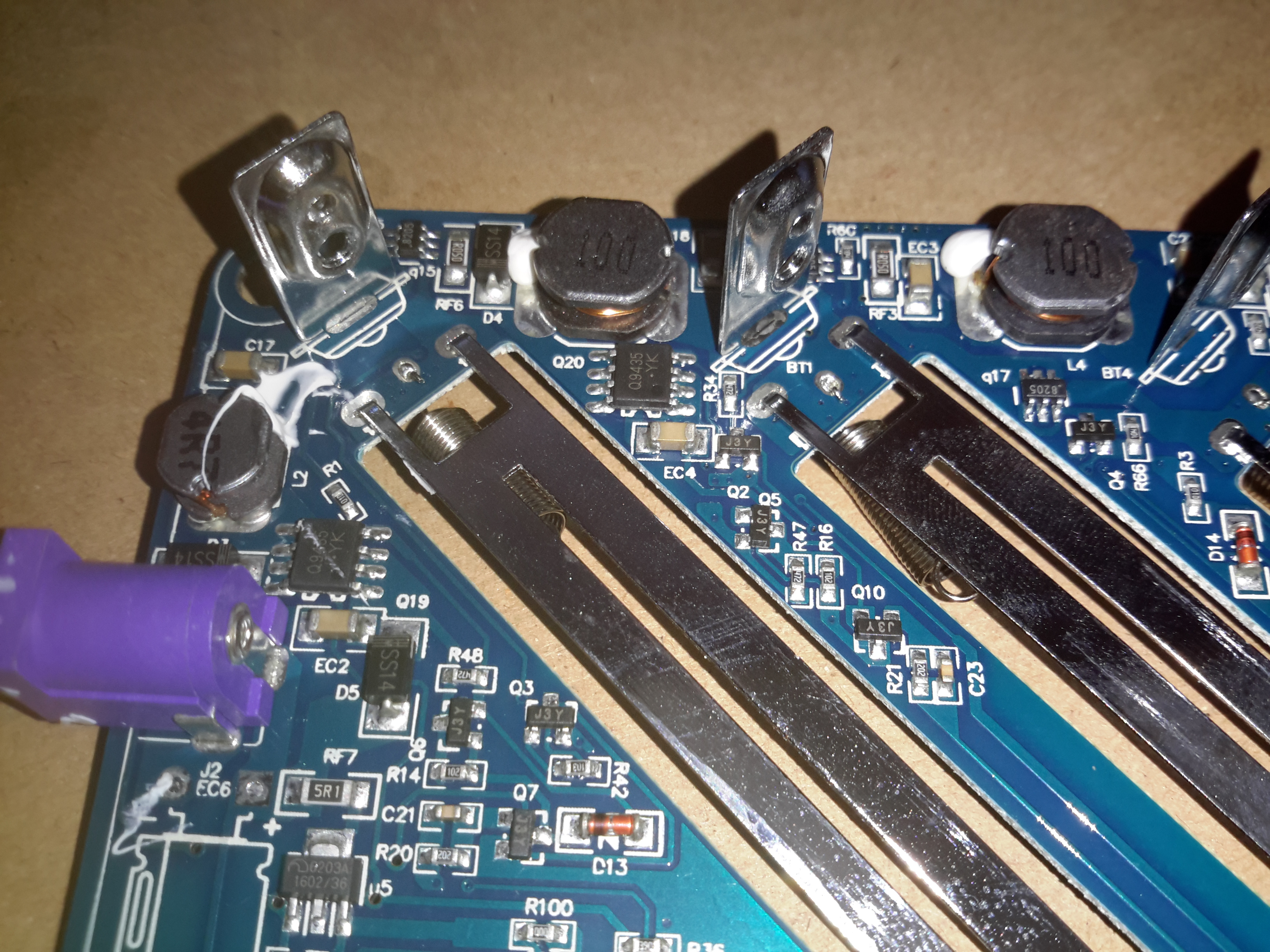
The main PCB is easily removed after the springs are unhooked from the terminals. Most of the power circuitry is located on the top side near the power input. There are 4 DC-DC converters on board for stepping the input 12v down to the 4.2v required to charge a lithium cell.
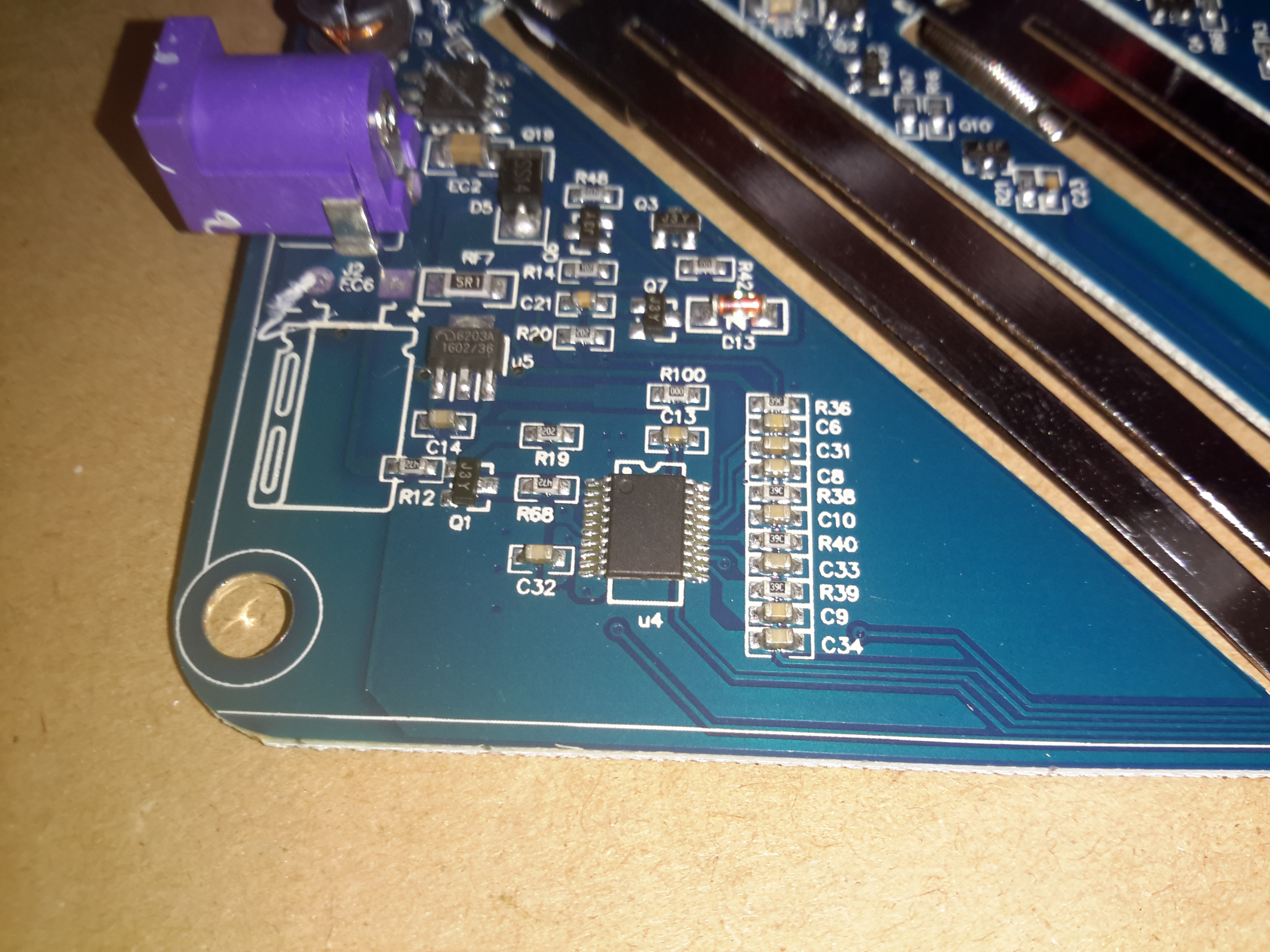
Second Controller
Not entirely sure what this IC is in the bottom corner, as it’s completely unmarked. I’m guessing it’s a microcontroller though.
DC Input Side
The top left of the board is crammed with the DC-DC converters, all the FETs are in SO8 packages.
DC-DC Converters
One pair of DC-DC inductors is larger than the other pair, for reasons I’m unsure of.
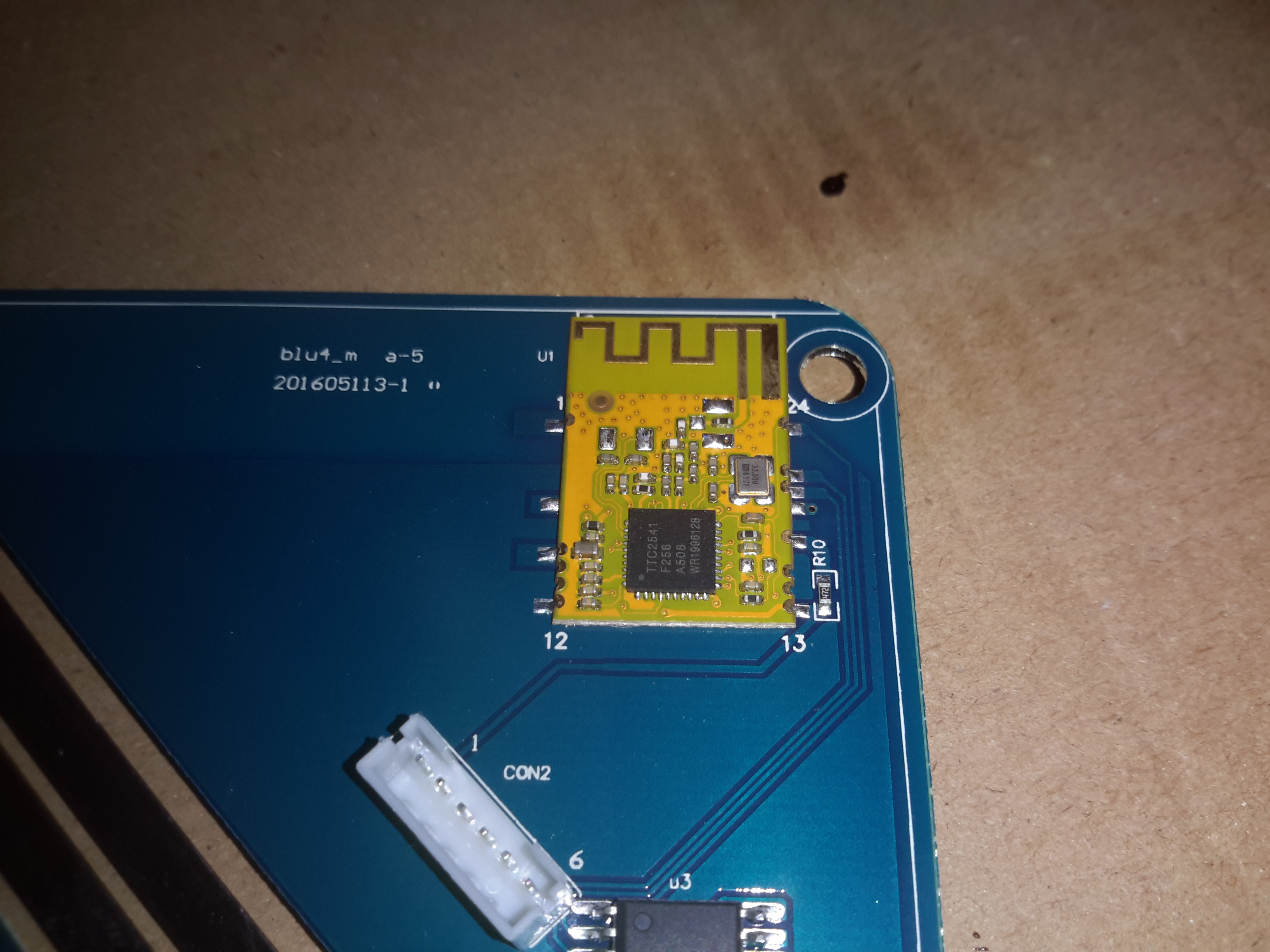
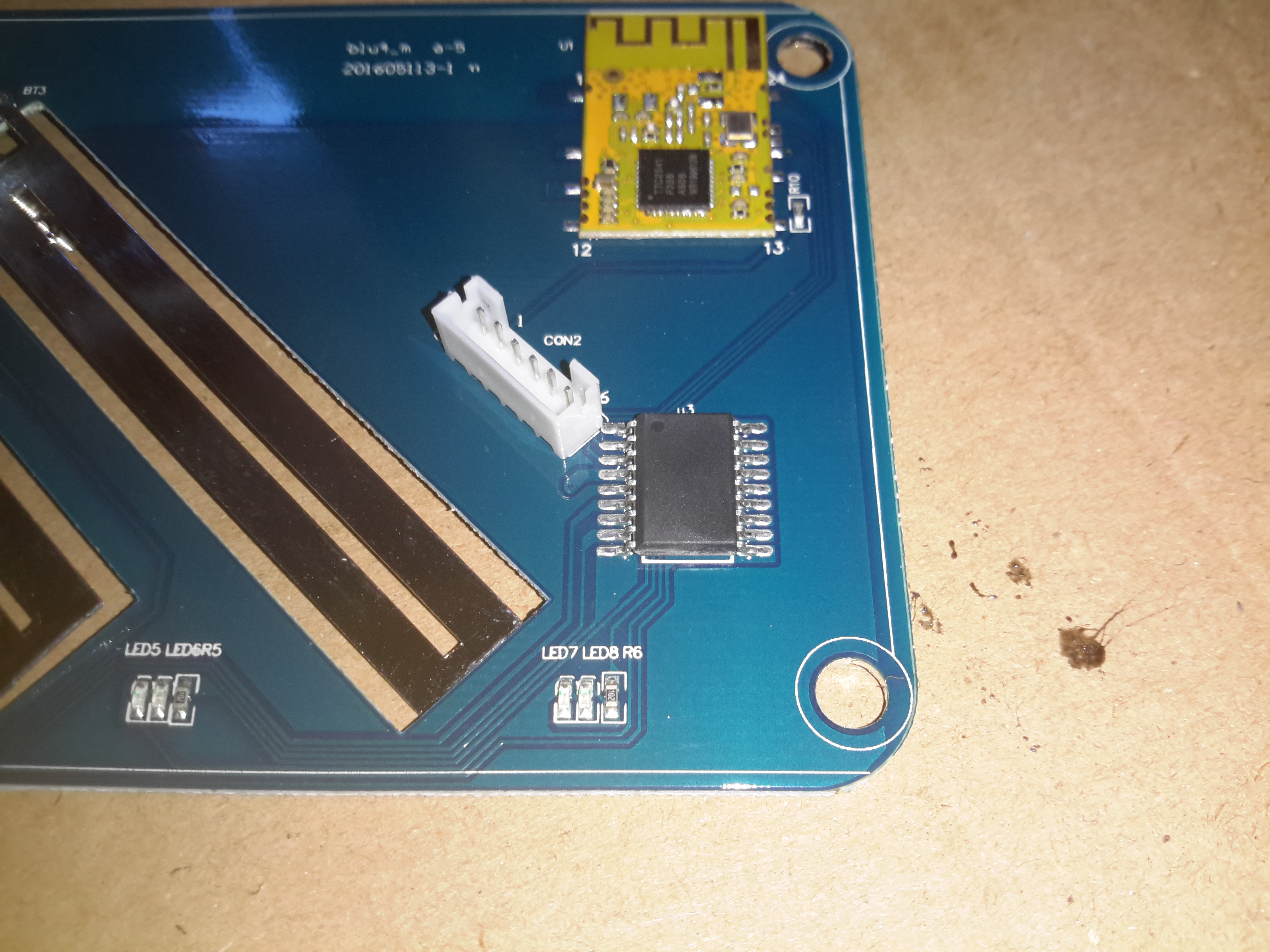
Bluetooth Module
Bluetooth connectivity is provided by this module, which is based around a TTC2541 BLE IC.
Microcontroller
Below the Bluetooth module is yet another completely unmarked IC, the direct link to the BLE interface probably means it’s another microcontroller. The Socket to the left of the IC is the connector for the front panel LCD & button.
LCD PCB
There’s not much to the LCD itself, so I won’t remove this board. The LCD controller is a COB type device, from the number of connections it most likely communicates with the micro via serial.
For the latest big project, replacing the battery bank on the boat with 5 brand new 200Ah Yuasa heavy duty flooded lead acids, I’m going to need to make many short links from heavy battery cable to connect all 5 batteries into a parallel bank.
Cutting cable as big in diameter as a good sized thumb is difficult at best. In the past I’ve used a hacksaw, but it doesn’t do a very clean job, especially as the cut nears the end – strands get ripped from the cable by the relatively coarse blade & this reduces the current carrying capacity.
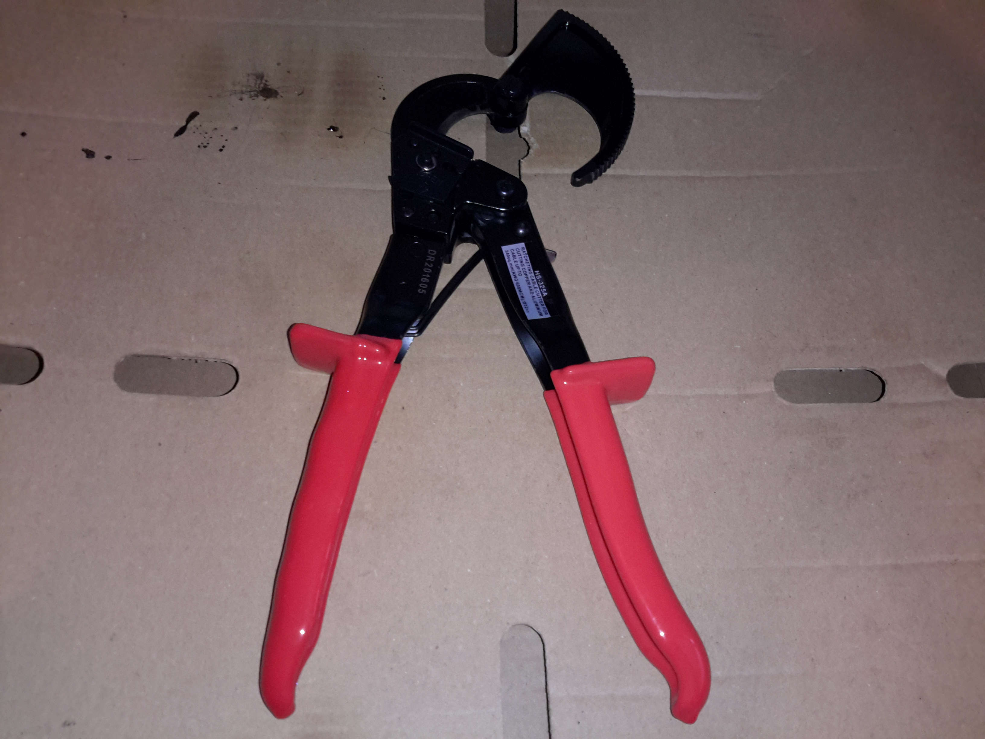
Over to eBay again netted a pair of ratchet-type heavy duty cable cutters for £30. These are rated to cut cable up to 240mm² or 600MCM.
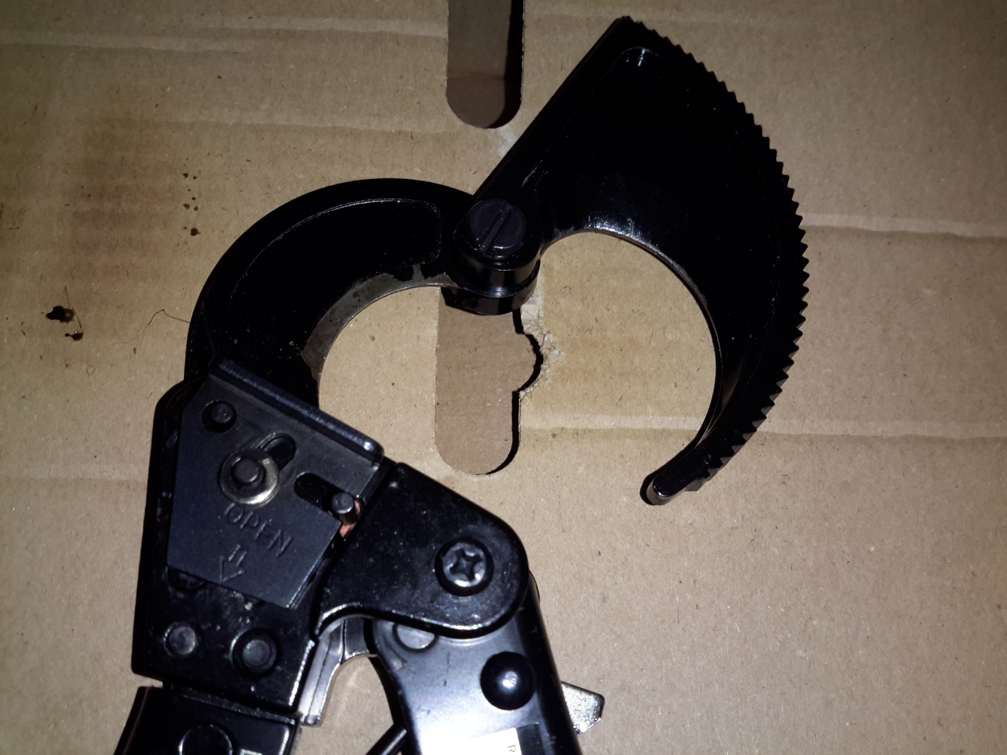
Cutting Jaws
The cutting head on these snips is massive – cutting through cable up to 35mm in diameter takes some force. The ratchet mechanism is used to get a large mechanical advantage to force the cutters through the copper, without having to resort to more expensive & complex mechanisms such as hydraulics. (Hydraulic cable cutters do exist, but cost a small fortune & are totally over-rated for the job).
Overall the tool seems to be well made, the handles are Vinyl dipped to make them more comfortable, which certainly helps when applying a large amount of force. Running a file over the cutters themselves reveals they’re actually hardened – unusual for cheapo Chinese tools.
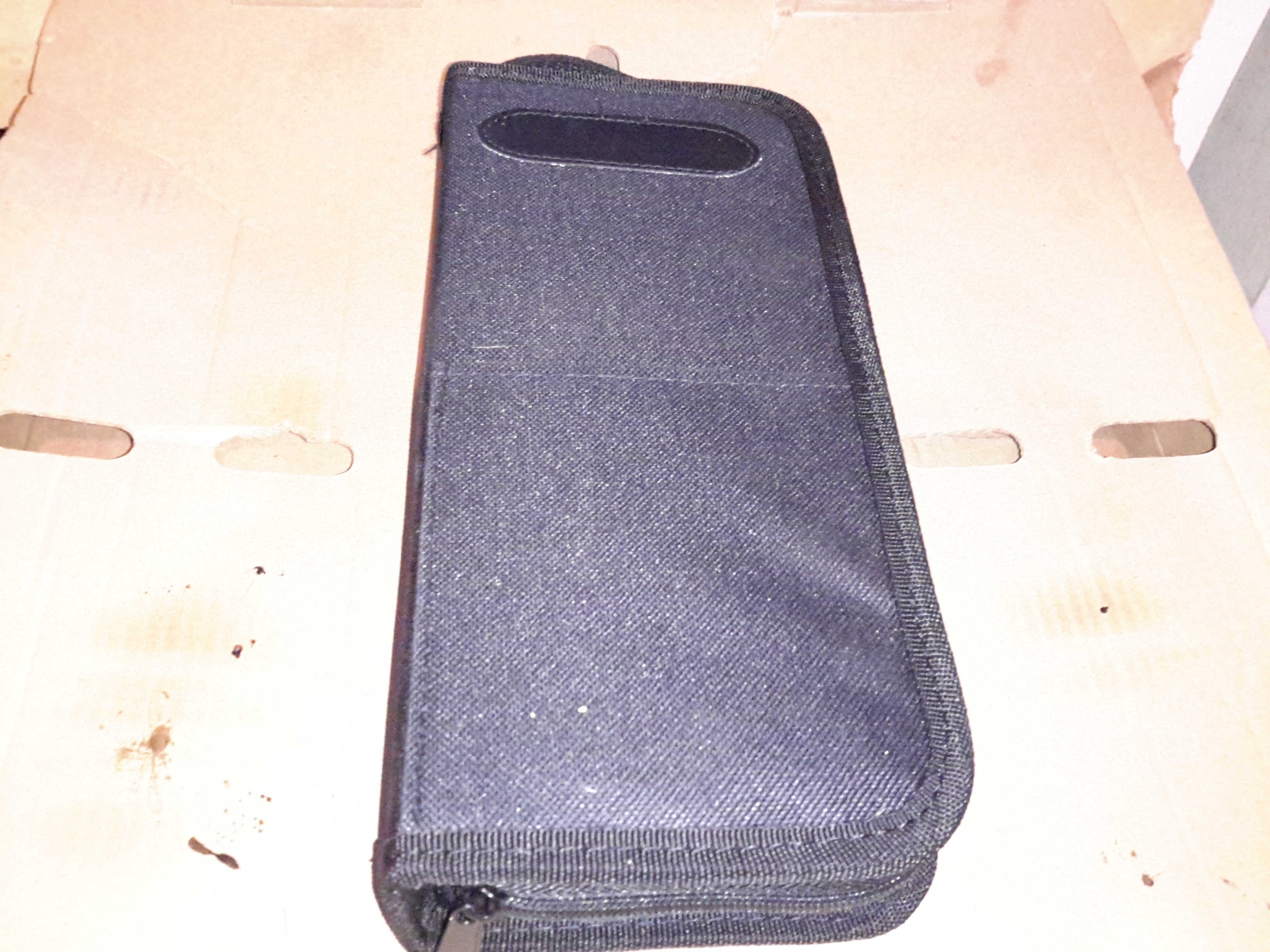
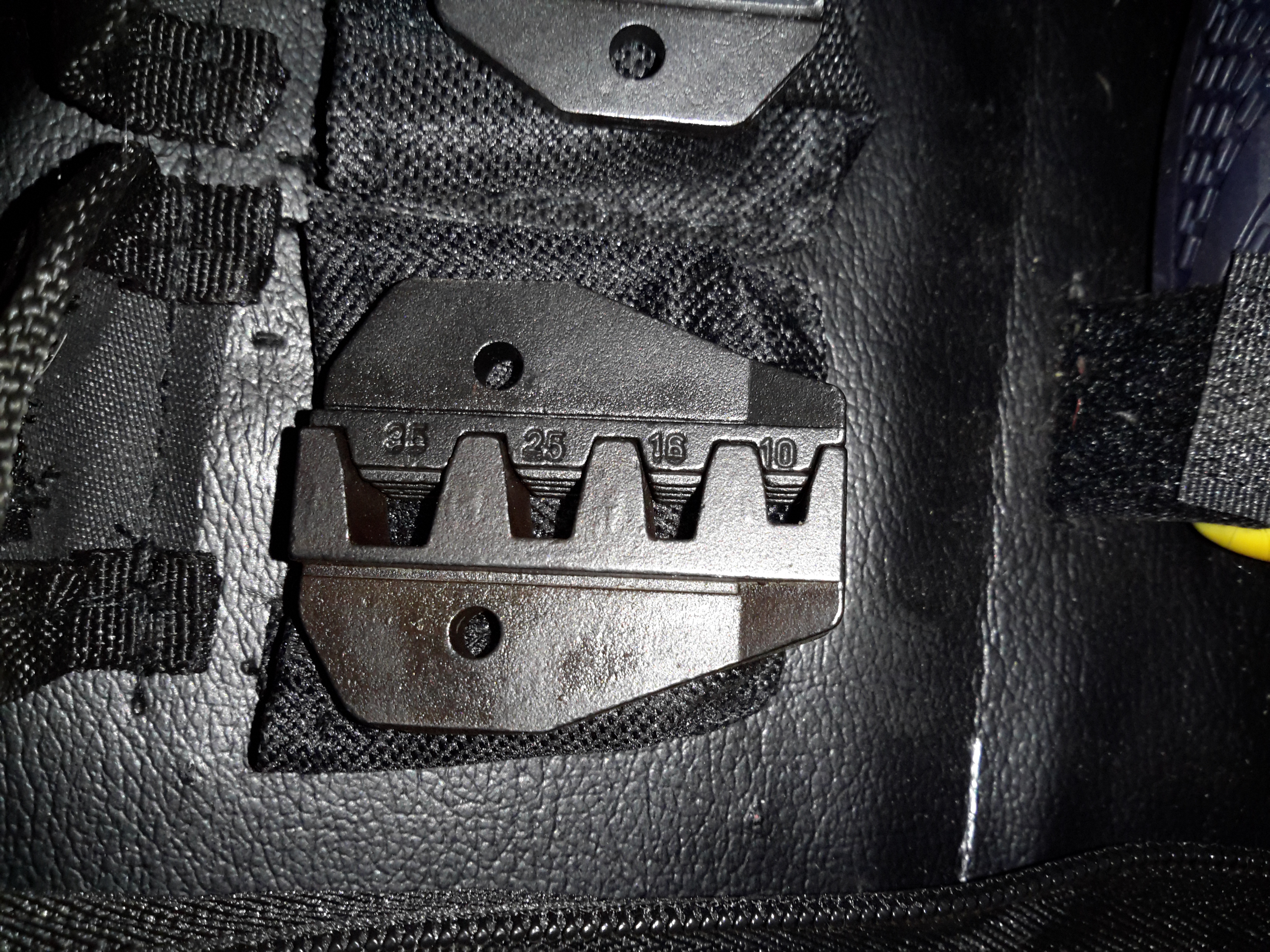
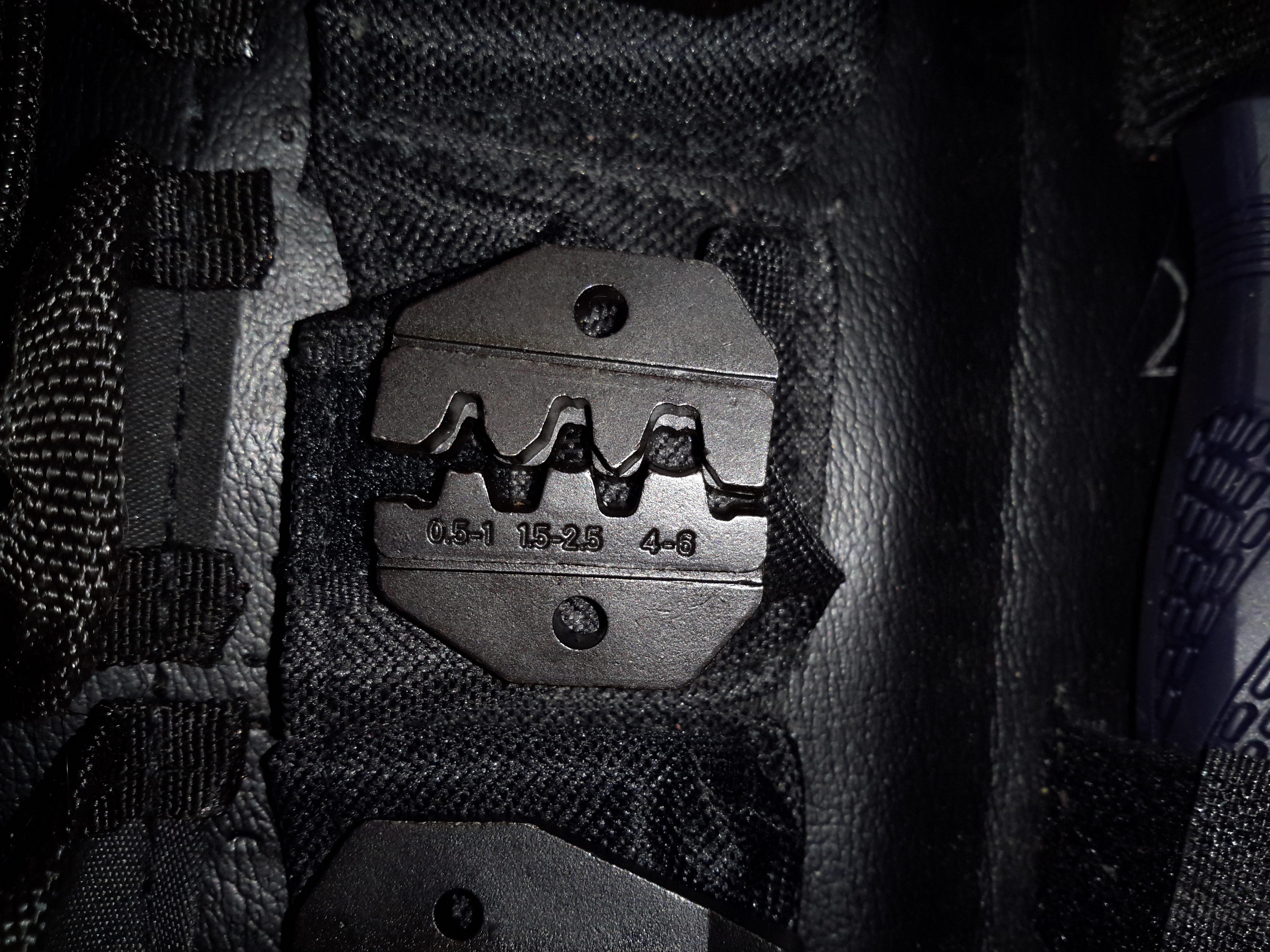
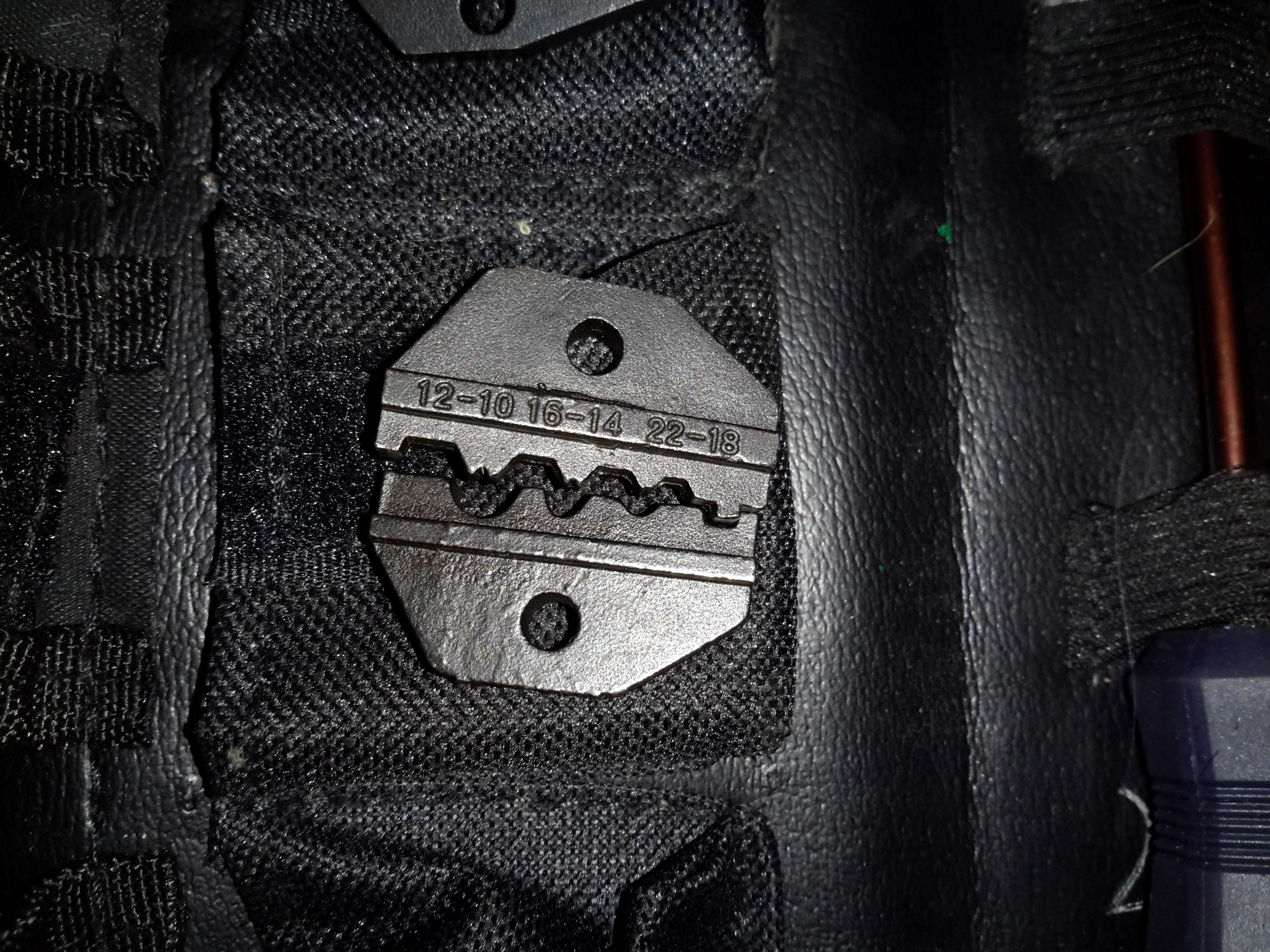
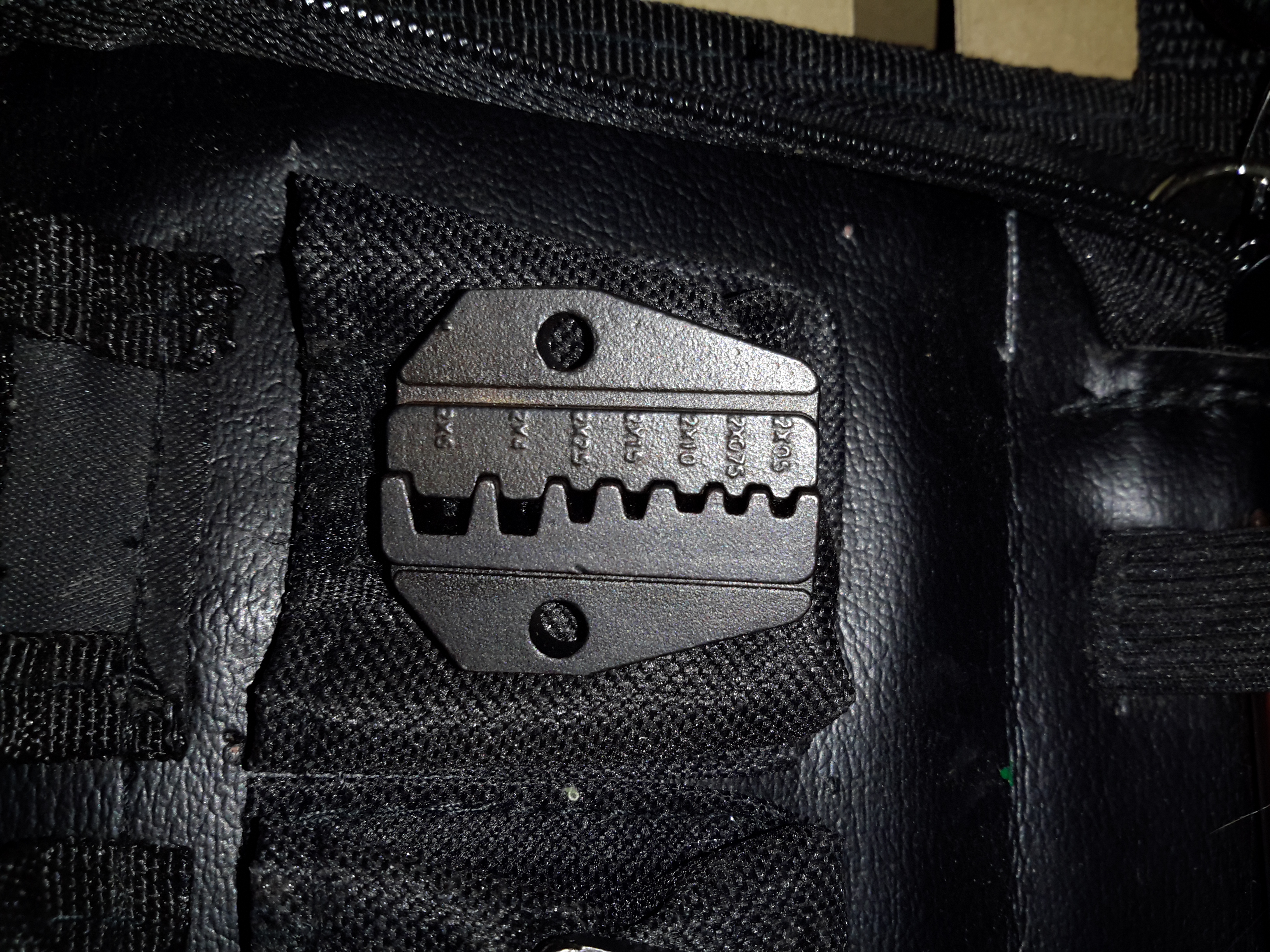
I recently decided to restock my toolkit, as there are plenty of jobs I need to sort that require the use of crimp terminals, so eBay again came to the rescue.
In my experience, cheap tools of any flavour are usually universally shite – I’ve had drill bits made out of a metal softer than aluminium, that unwind back into a straight flute bits as soon as they’re presented with anything harder to drill through than Cheese. Ditto for screwdrivers. But for once the far eastern factories seem to have done a reasonable job on this crimp tool set.
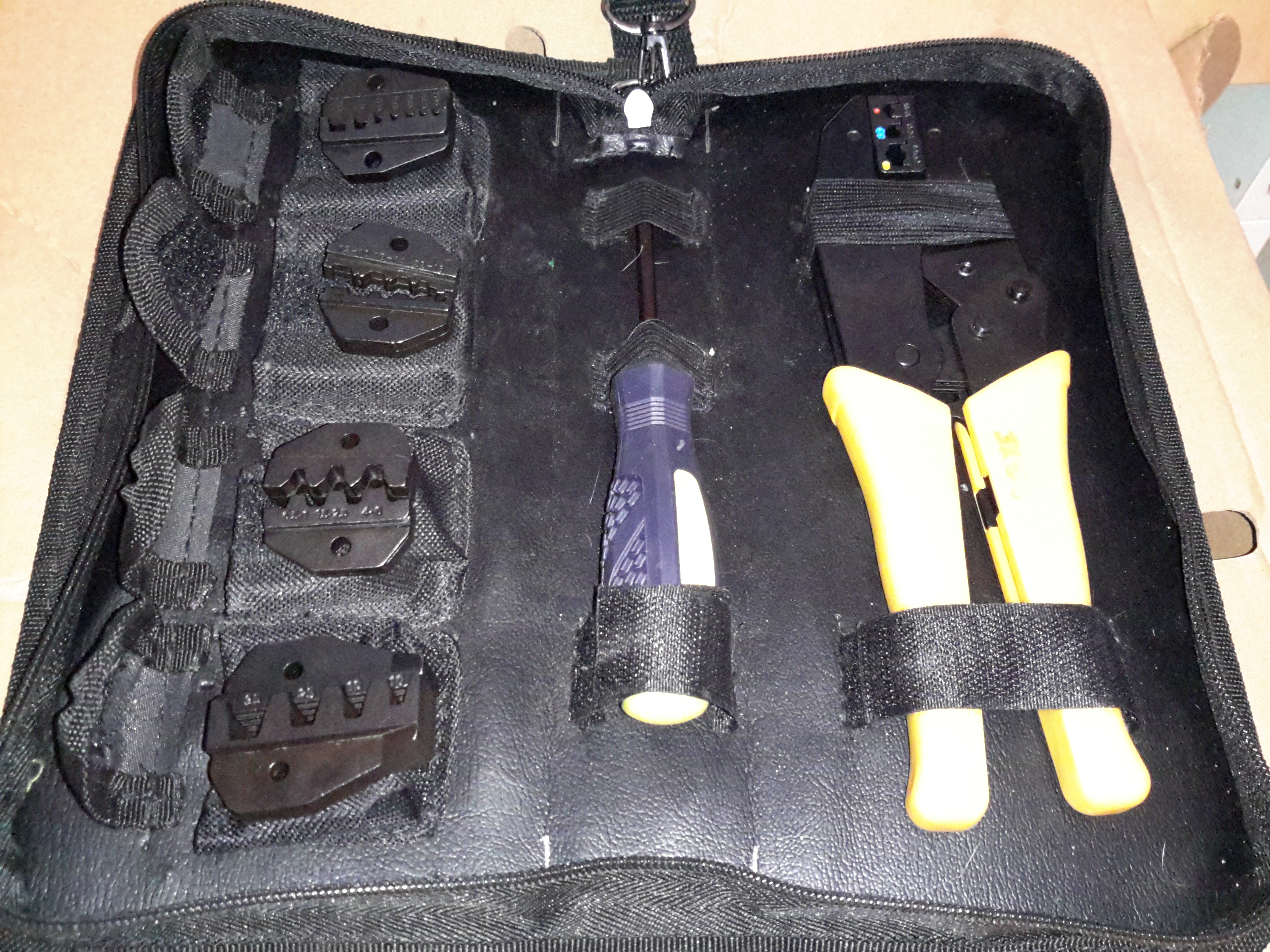
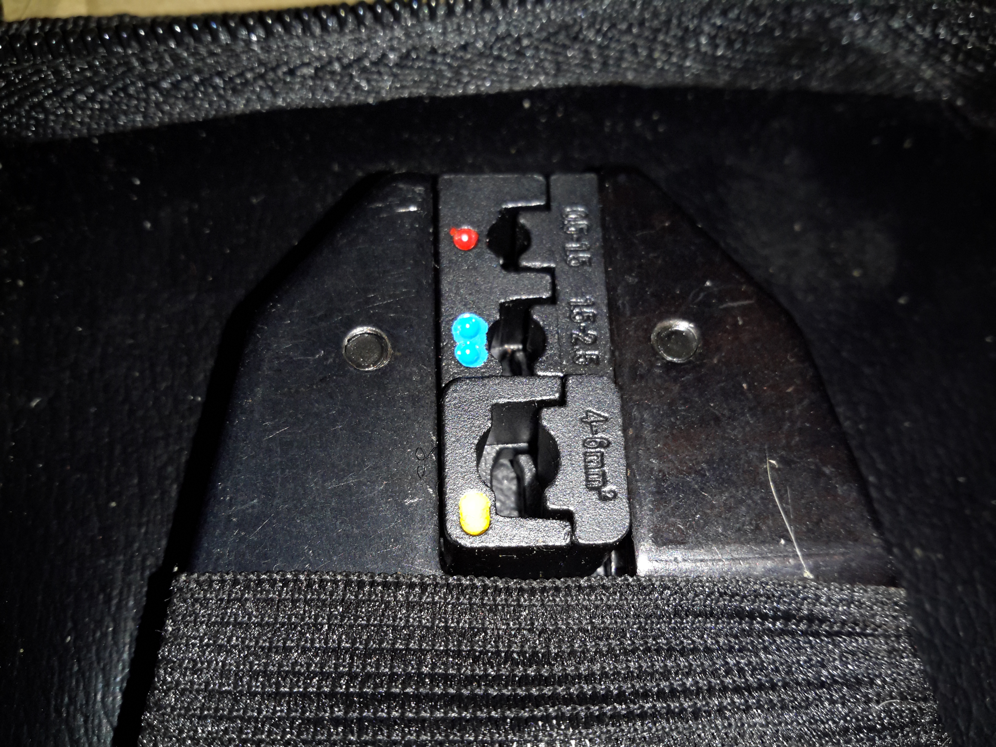
eBay Crimping Tools
These are ratchet type crimping pliers, with interchangable heads so many different types of terminals can be used. A handy Philips screwdriver is included in the kit for changing the dies.
Large Dies
The largest dies in the set can handle cable up to 25mm² – just about the bottom end of main battery cables, which is very handy.
Medium Dies
Smaller sets of dies are provided for other types of terminals.
Small Dies
I’m not precisely sure which type of terminals these dies fit – the profile is a bit unusual.
Tiny Dies
The smallest dies in the set are good for extremely small wires – down to 0.5mm
Automotive Dies
The pliers are supplied with the standard colour-coded automotive dies installed. Sometimes these terminals never crimp properly, as the dies just effectively crush the copper tube of the terminal, so more often than not the wire strands are just forced out of the terminal as the crimp is made, leaving a bad connection.
These are even better than the ratchet-type crimp tools at the local Maplin Electronics – the set of those I have just distorts when a large crimp is made, so the terminal never gets a full crimp. The steel is not stiff enough to handle the forces required.
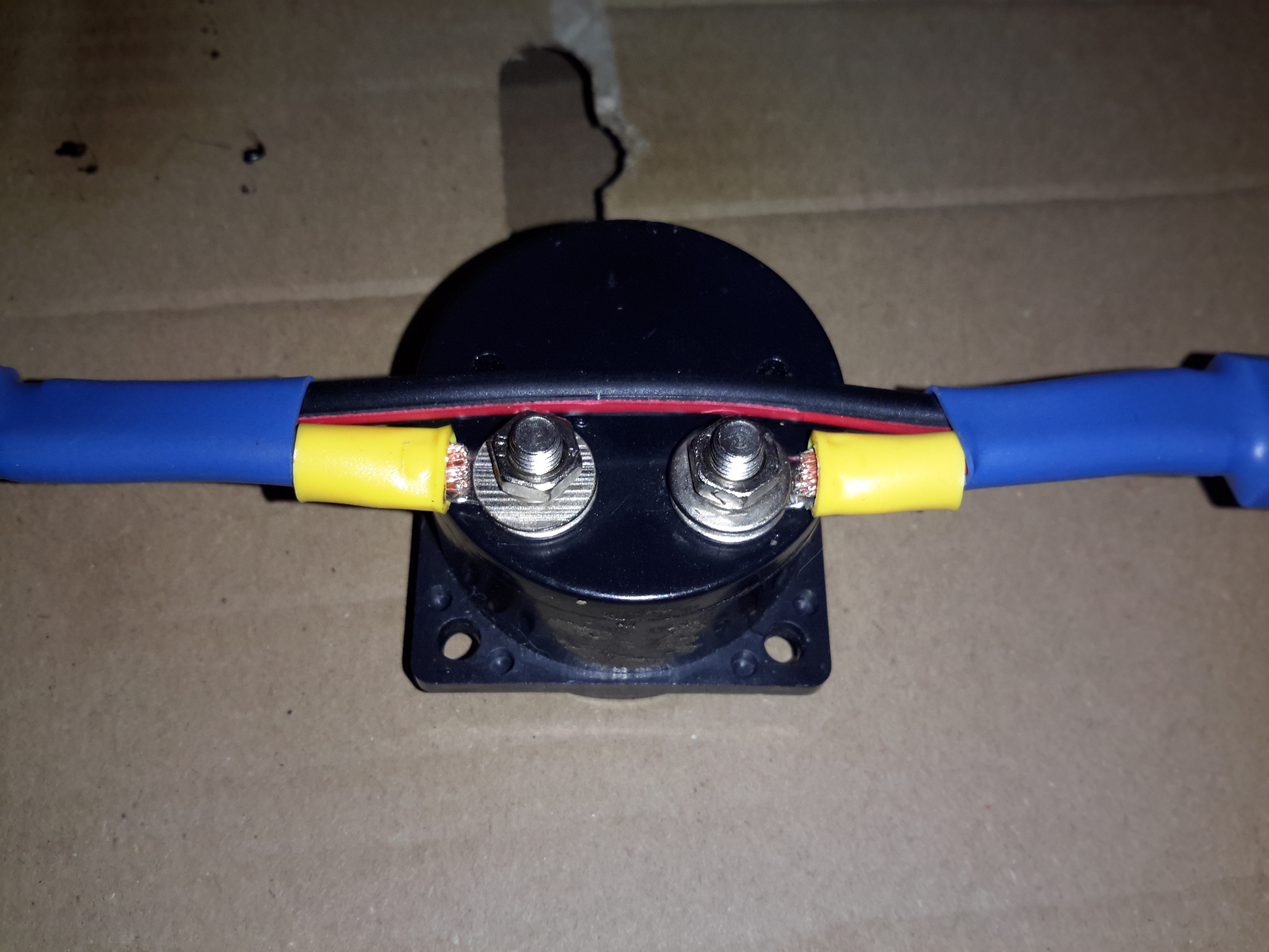
Example Crimp
Here’s a couple of large crimps on 6mm² cable attached to an ammeter. The crimps are nice & tight & hold onto the cable securely. The insulating sleeve on the terminals also hasn’t been cut through by the dies, which is often a problem on cheap crimp tools.
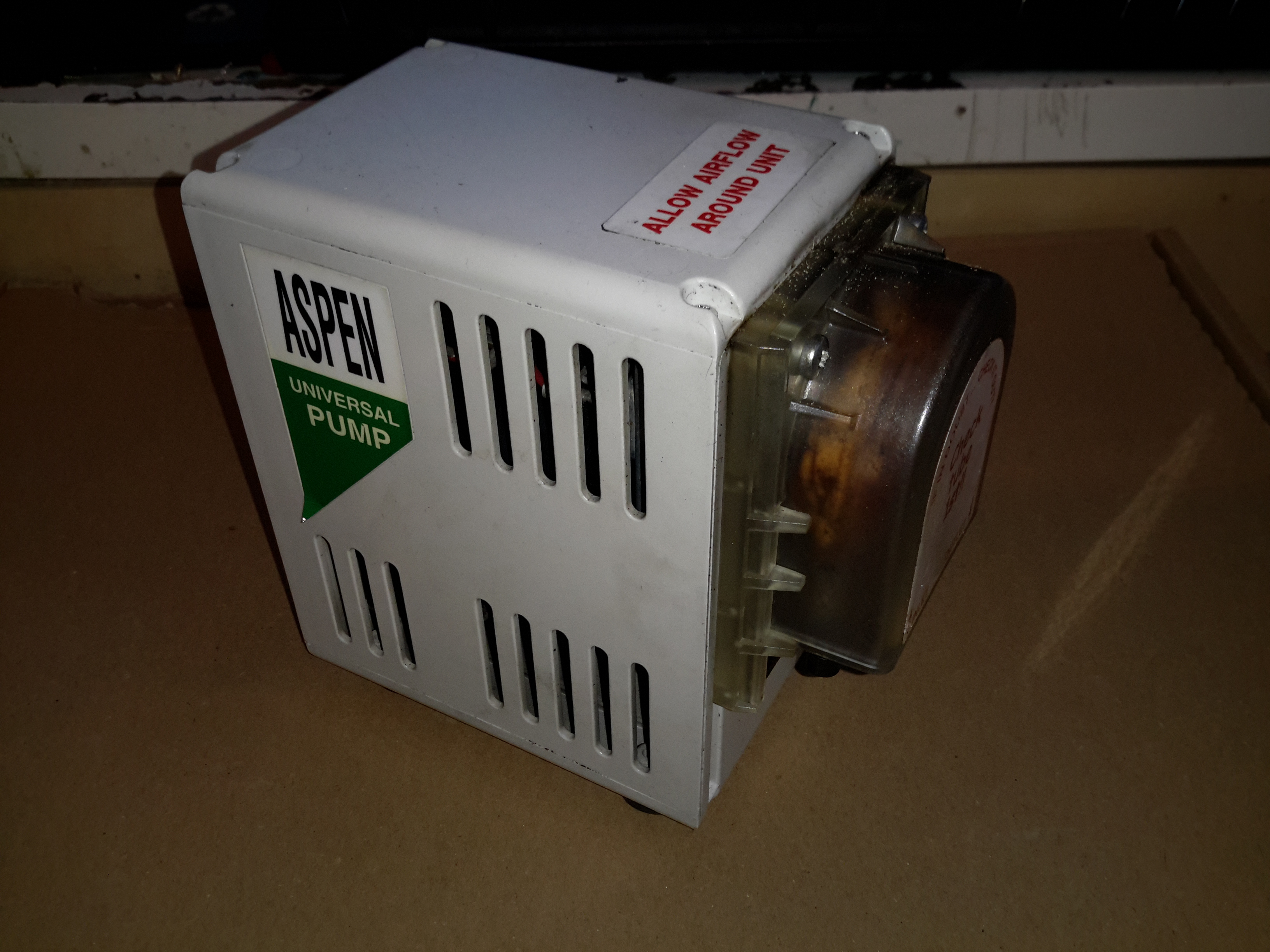
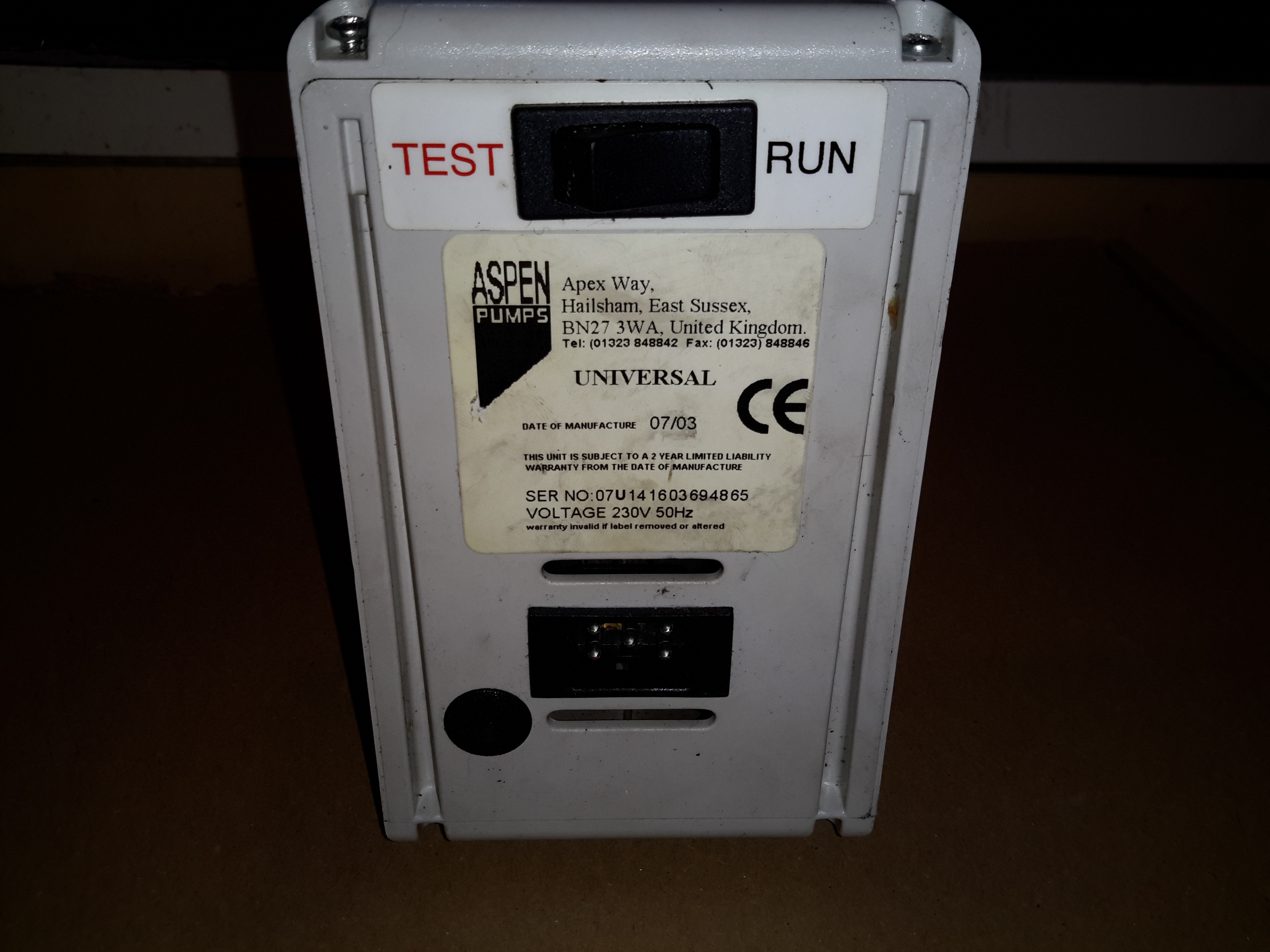
Here’s another piece of commercial gear, from an industrial air conditioning unit. These pumps are used to drain the condensate from the evaporator unit, so water doesn’t end up raining down from the ceiling.
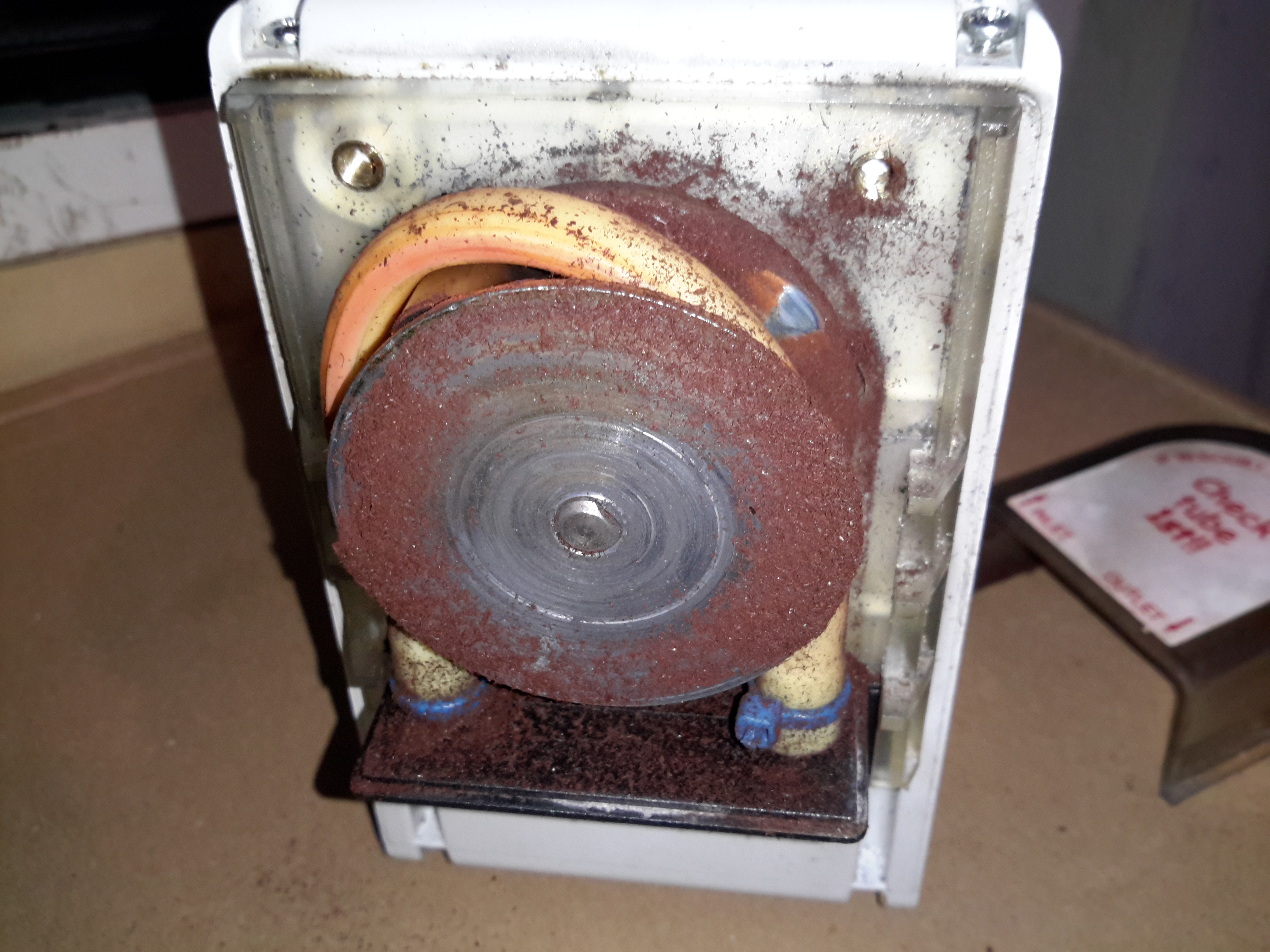
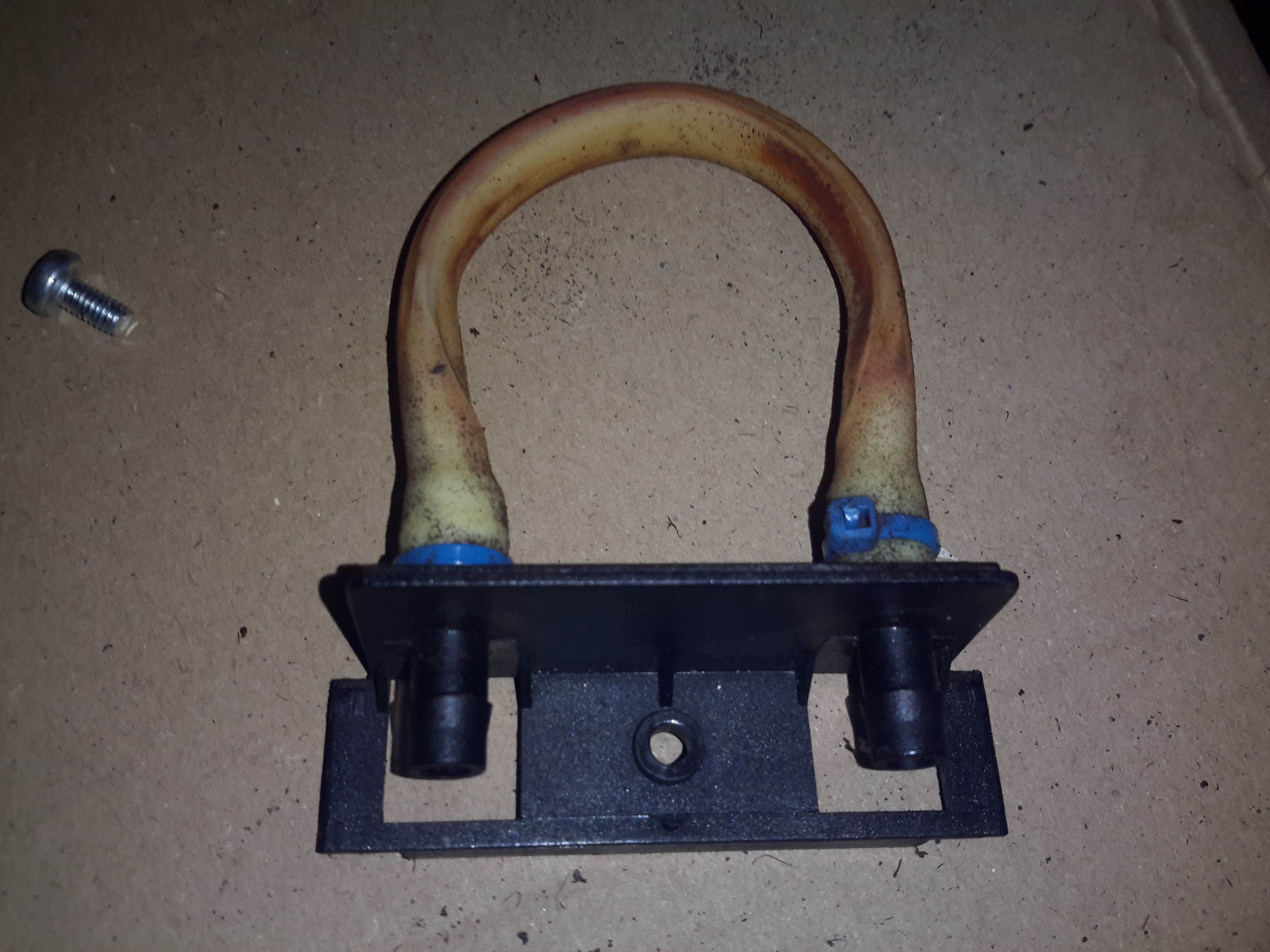
Pump Head
This is a peristaltic pump, with a silicone hose forming the pumping element.
Rear Panel
The test switch & electrical connections are on the back, along with the data label.
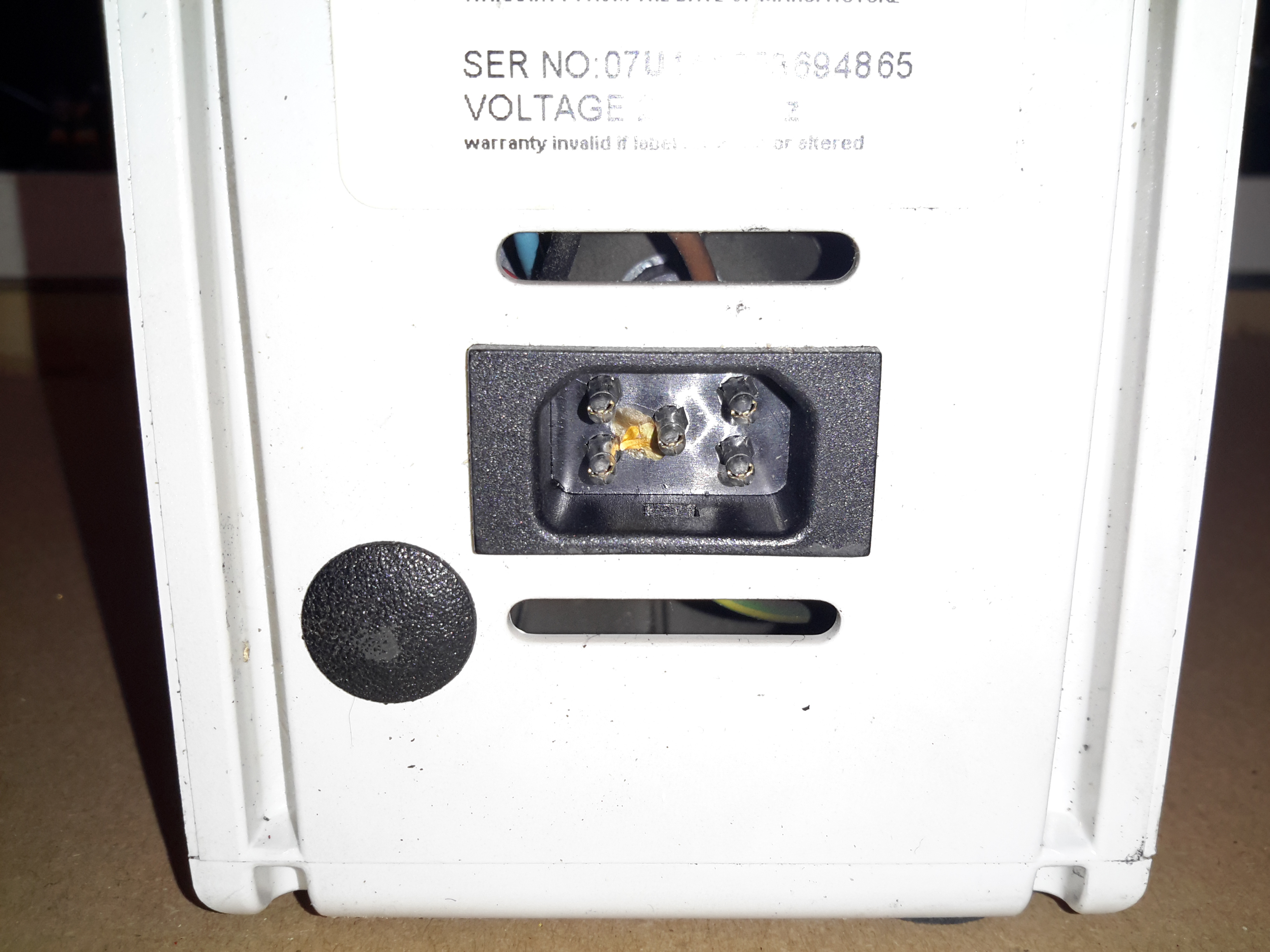
Power & Sensor Socket
The electrical connections are all on a single 5-pin socket. Along with 240v AC mains, there are a pair of thermistors connected to the unit, which switch the pump on when a 5°C temperature difference across the evaporator coil is detected. When air is cooled, it’s capacity for moisture drops, so the water condenses out on the coil.
Roller Wheel
Here the front cover has been removed from the pump, showing the silicone tube & roller wheel. The wheel was originally Cadmium-plated, but exposure to the elements has oxidized this into highly toxic Cadmium Oxide.
Pump Rollers
Here you can see the rollers. These pinch the tube at the inlet, and the rotation carries a slug of liquid through the tube to the outlet side.
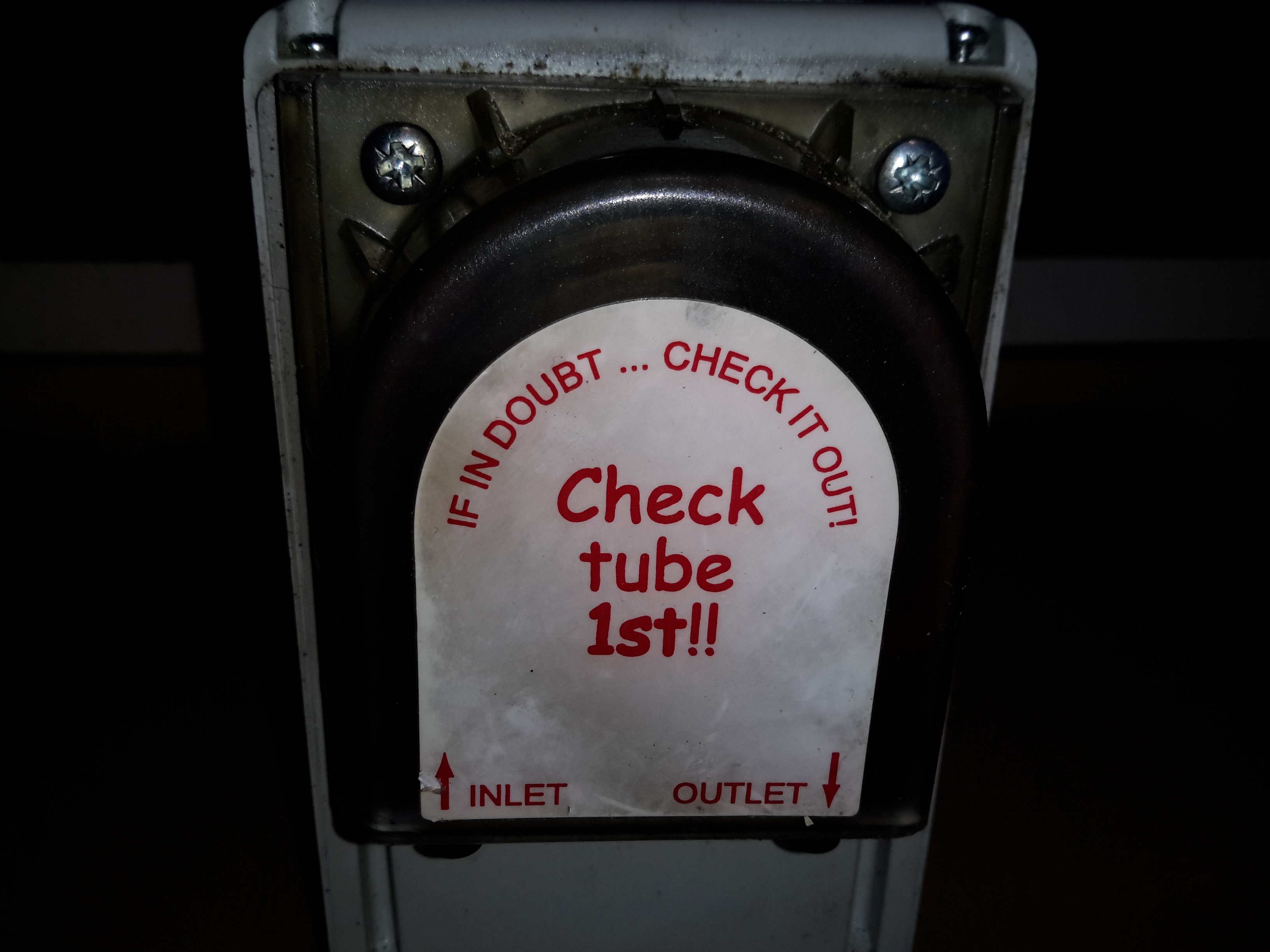
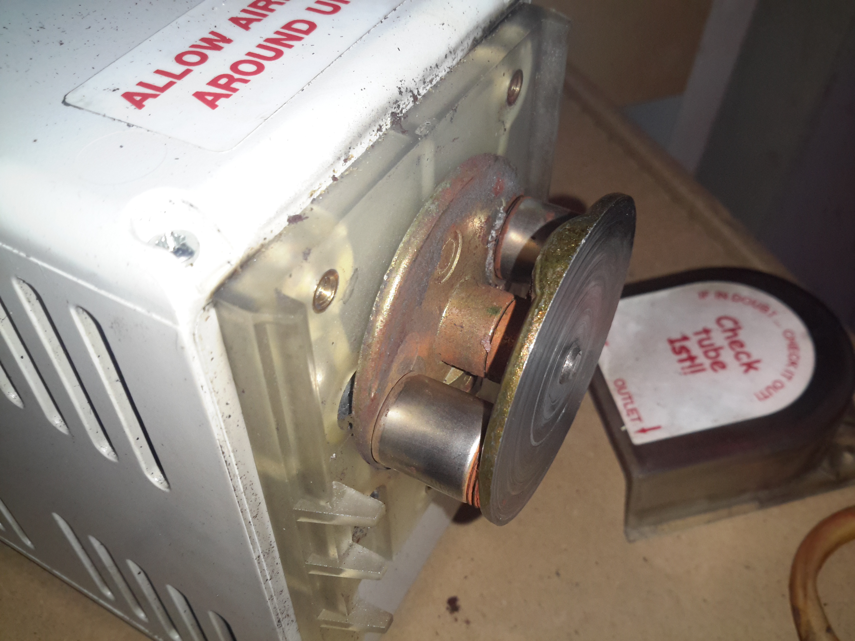
Pump Tube
Here’s the tube itself, the main wearing part of the pump. This is replaceable as a spare part.
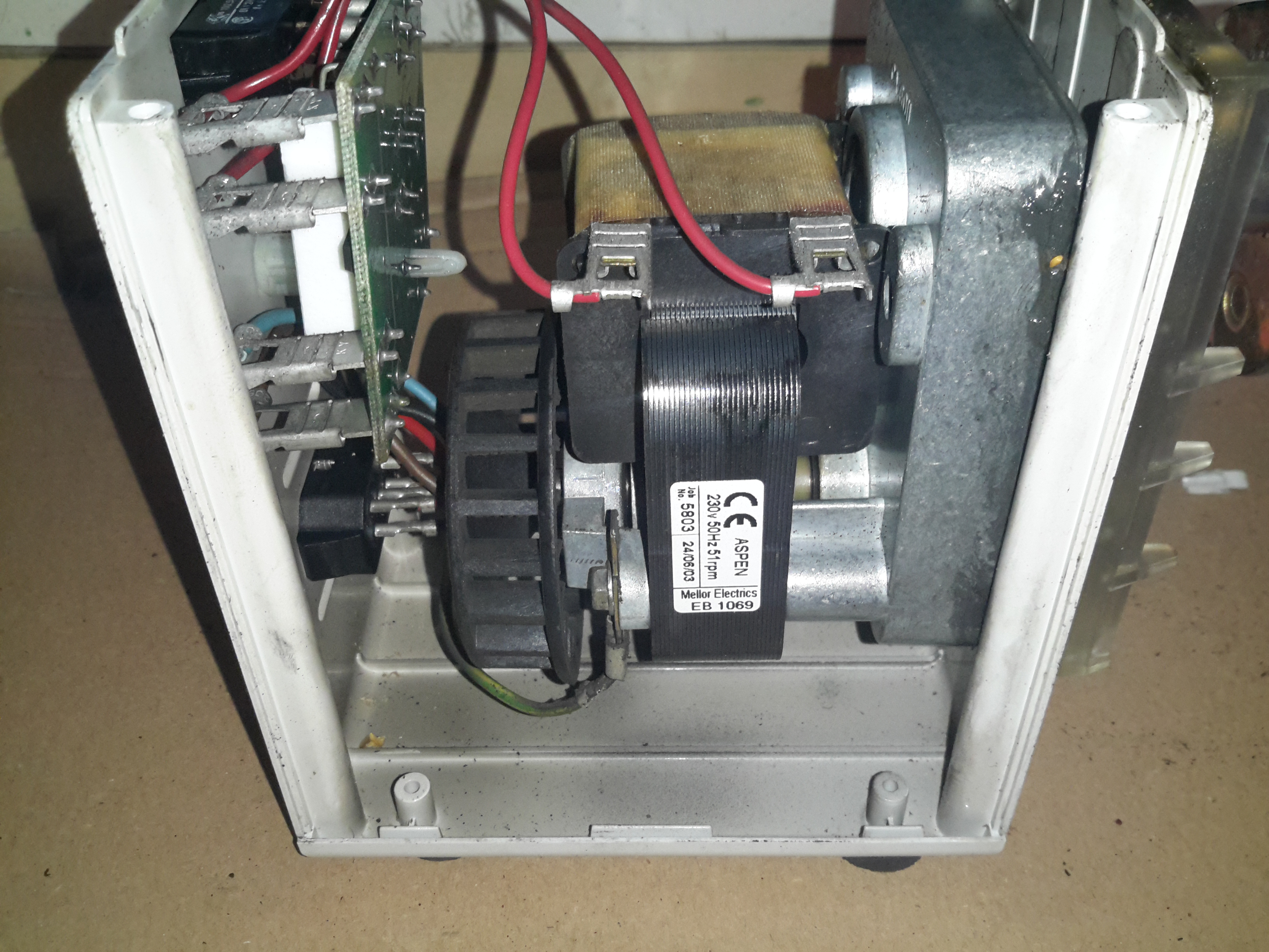
Motor & Gearbox
Inside the casing is a shaded-pole motor, connected to a large gearbox, to give the slow rotation for the pump head. The rated speed is 51RPM.
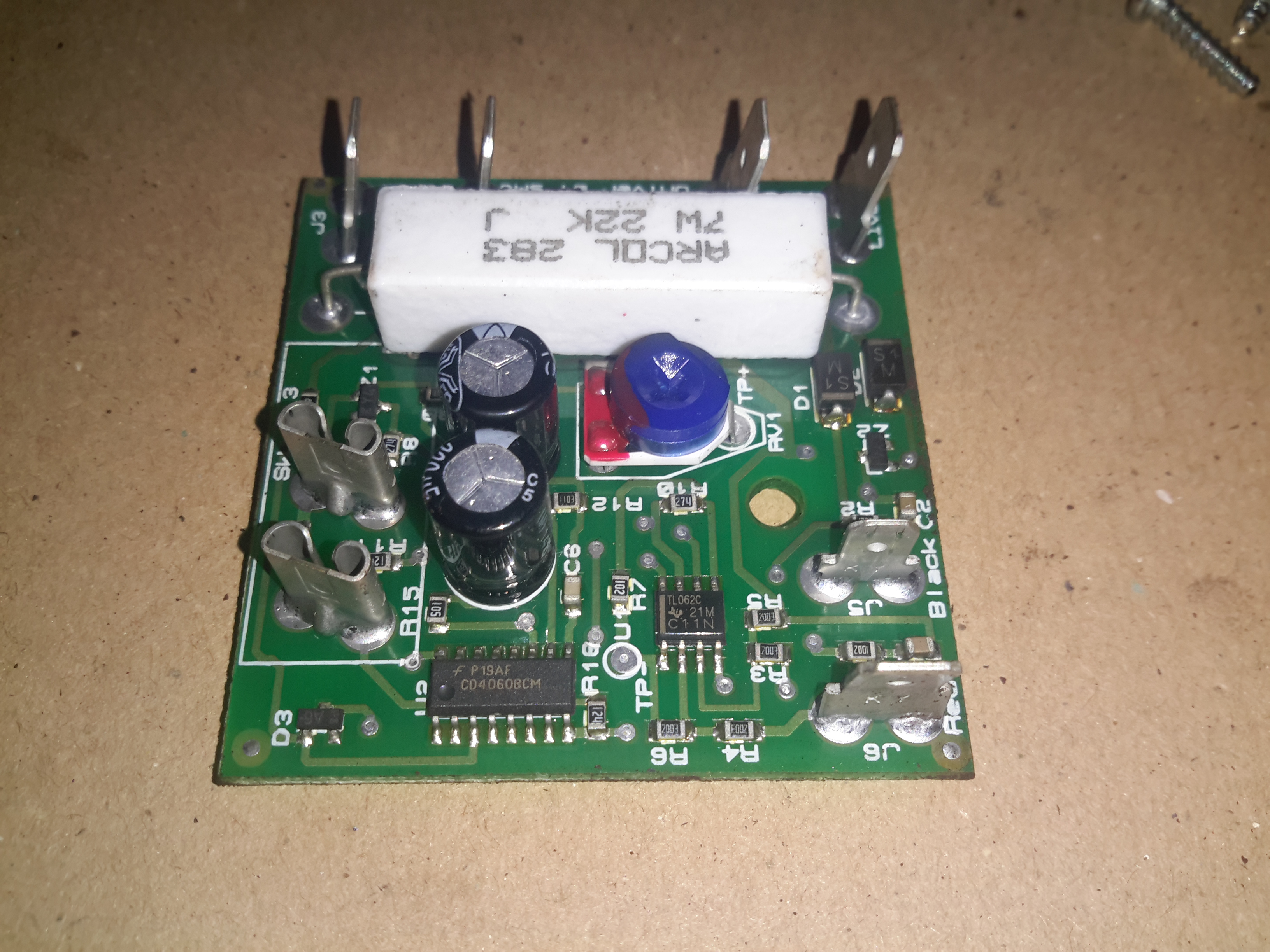
Control PCB
There’s not much to the control PCB. The large resistor forms a voltage dropper, to reduce the mains 240v to a more suitable level for the logic. There’s a TL062C Low-Power JFET Op-Amp & a CD4060BCM 14-stage binary ripple counter forming the logic. The set point is adjustable via the potentiometer.
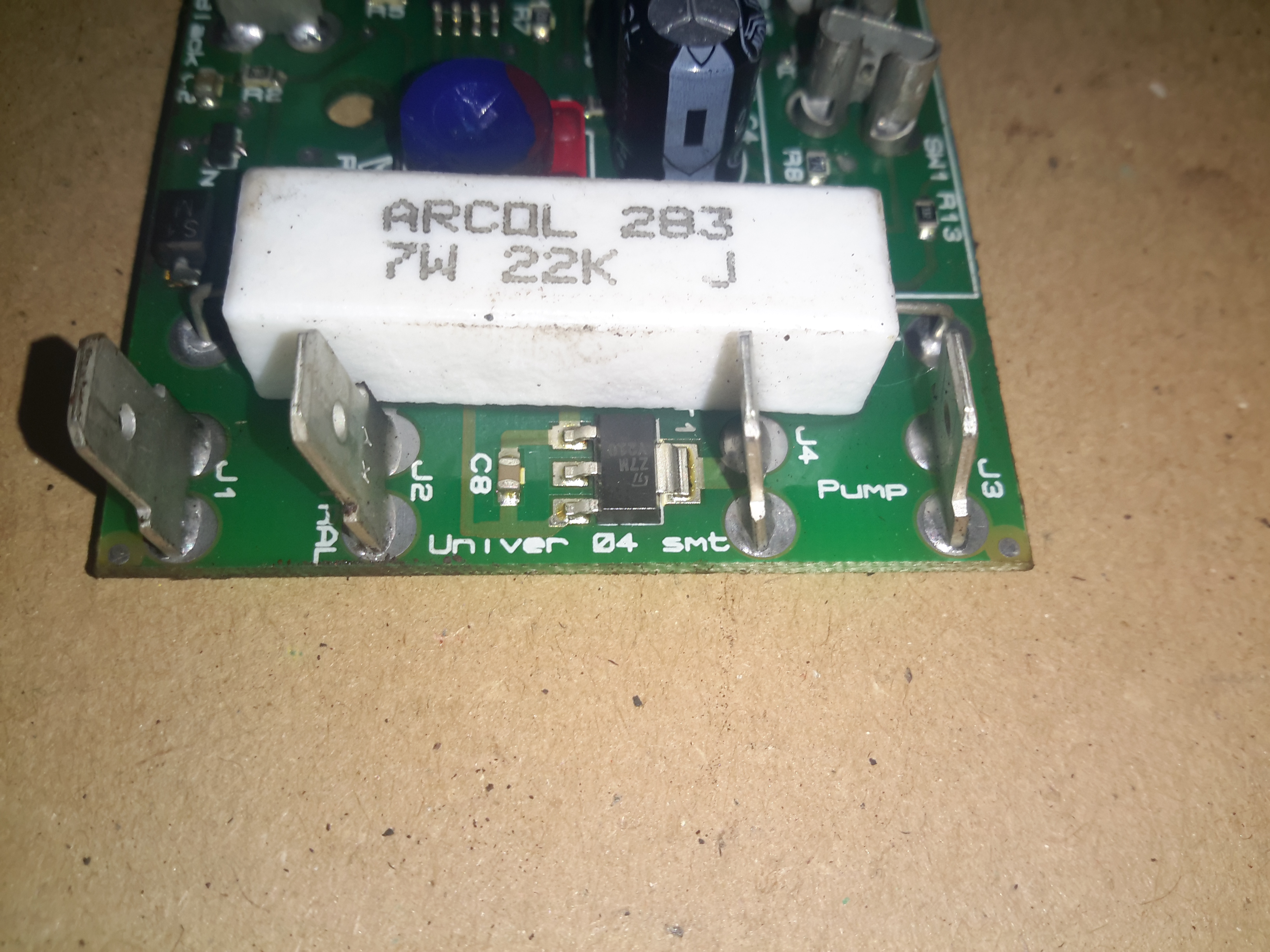
Pump Triac
The pump motor is switched via this Z7M SMD triac, not much switching power is needed here as the motor is only a very small shaded-pole type.
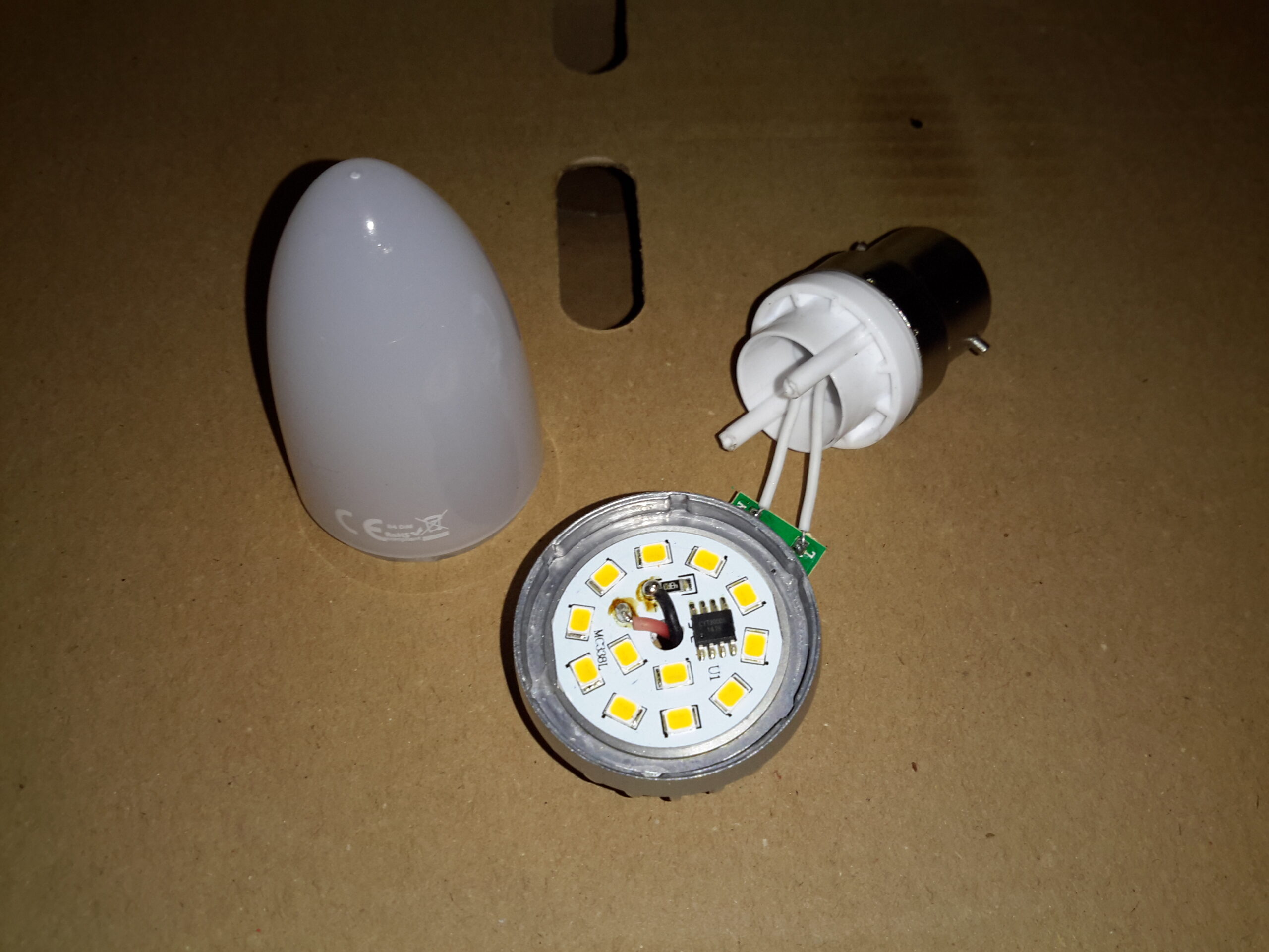
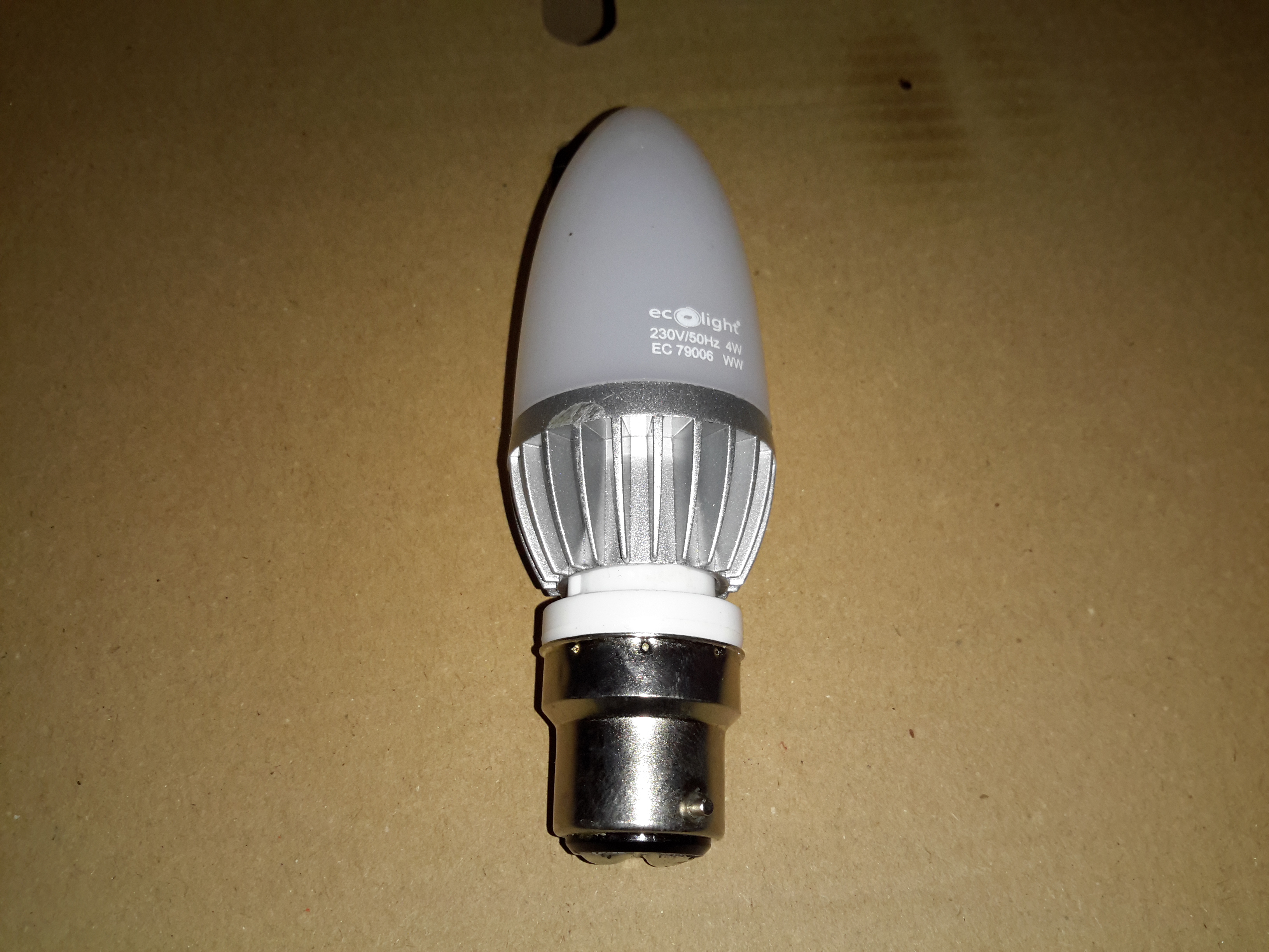
Here’s a modern LED bulb, that unfortunately decided to disassemble itself within a few minutes of being installed in a light fitting! The base plastic snapped off the main aluminium body at the screw posts!
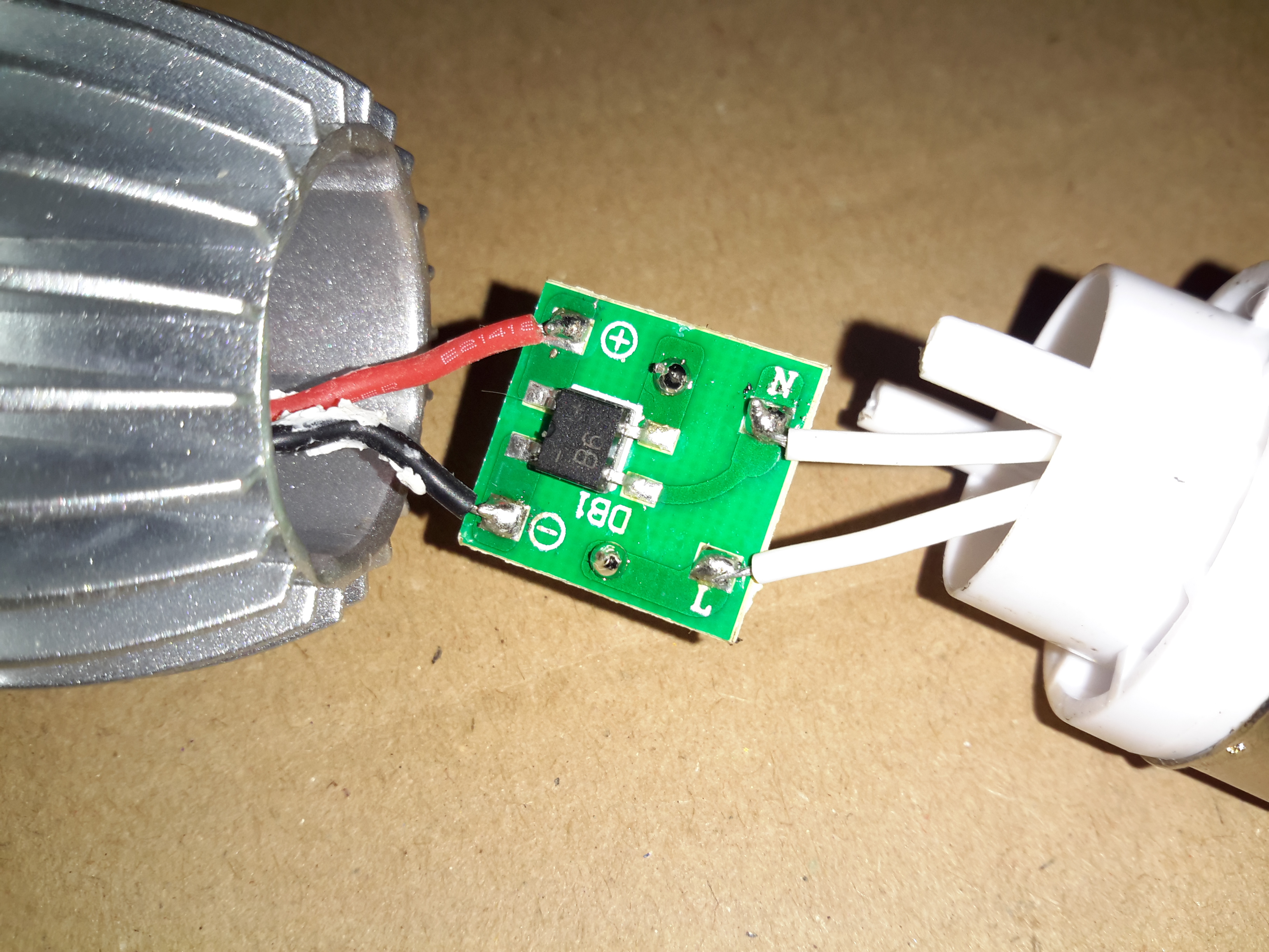
Input Rectifier
The PCB in the base holds nothing but the input components. Above is the bridge rectifier.
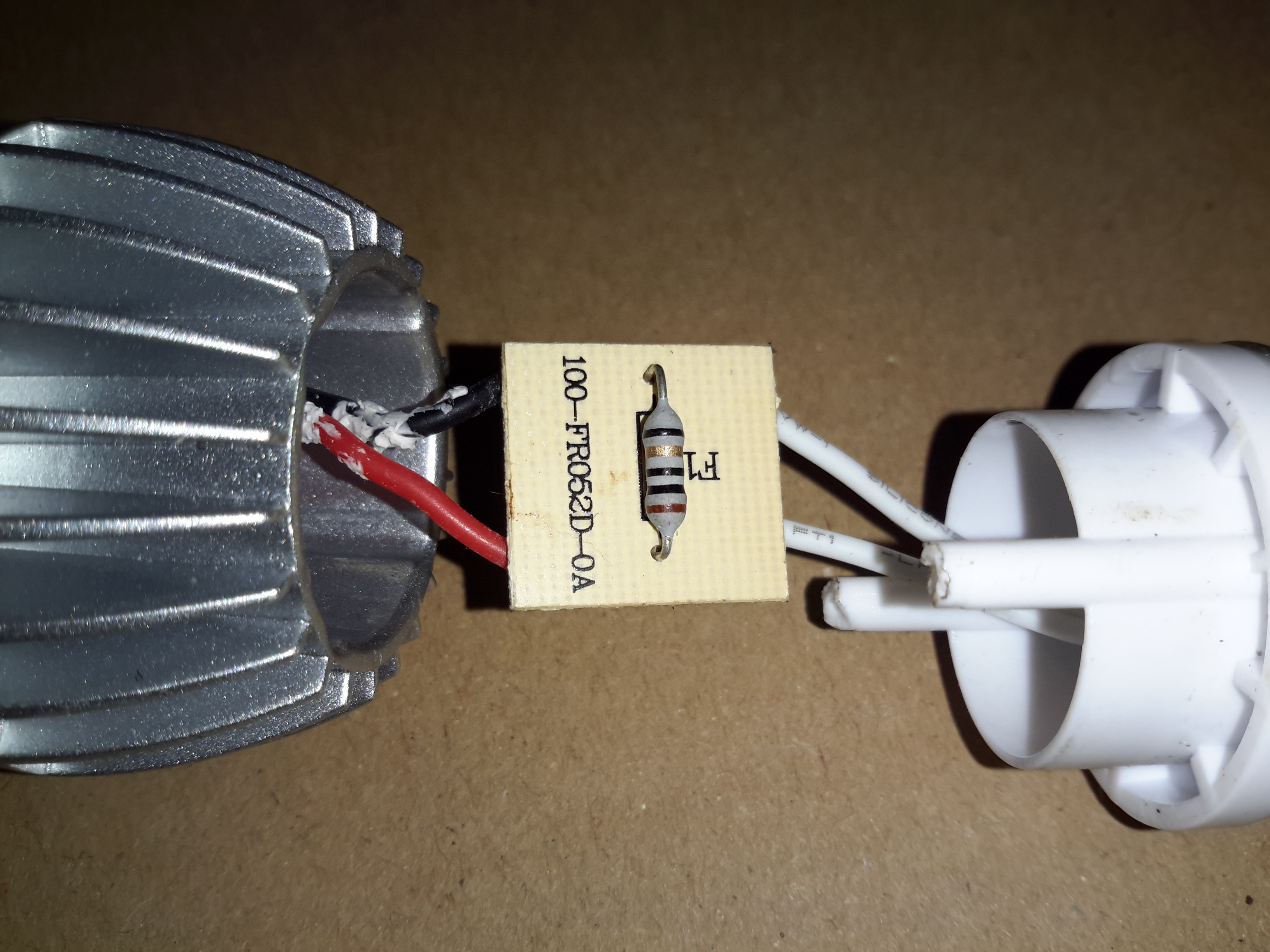
Fusible Resistor
The other side of the PCB has a 10Ω fusible resistor, for protection.
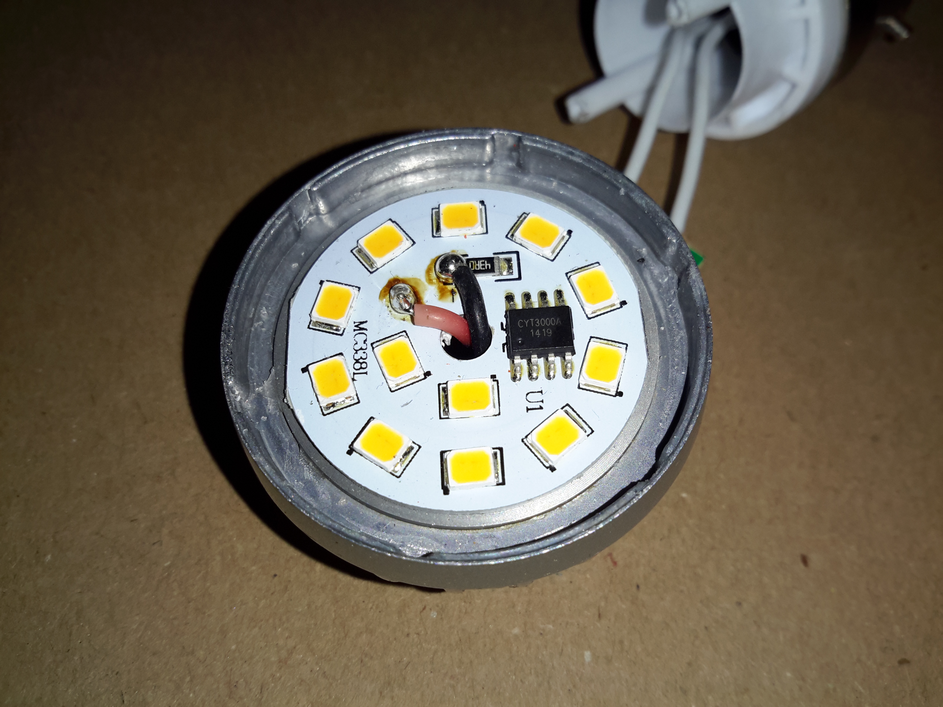
LED PCB
The LED PCB itself has the driver IC, which is a CYT3000A linear constant current IC, that runs direct from full-wave rectified mains. The single resistor sets the LED current, but there aren’t any smoothing capacitors on the DC rail, so this bulb would flicker a lot.
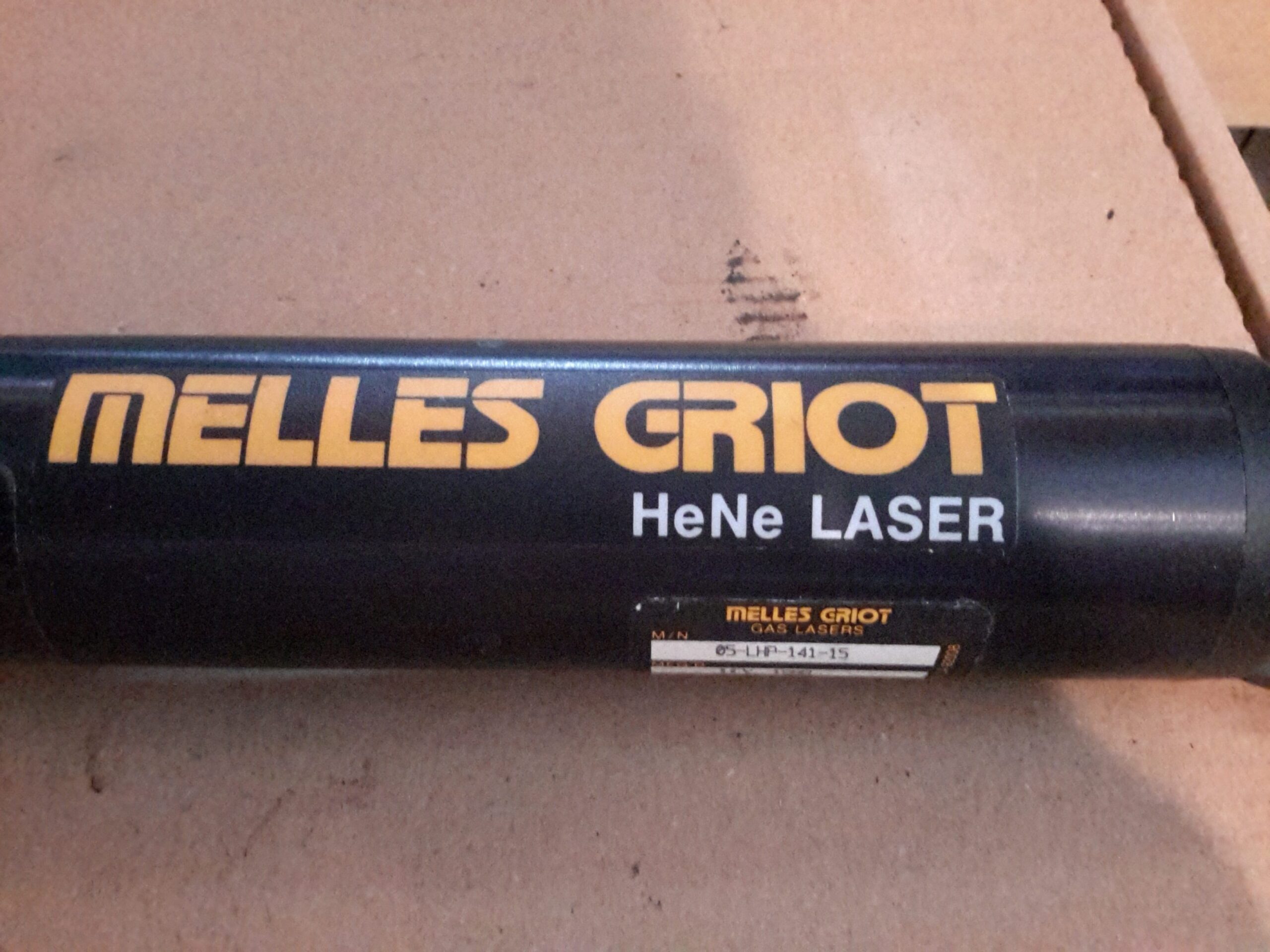
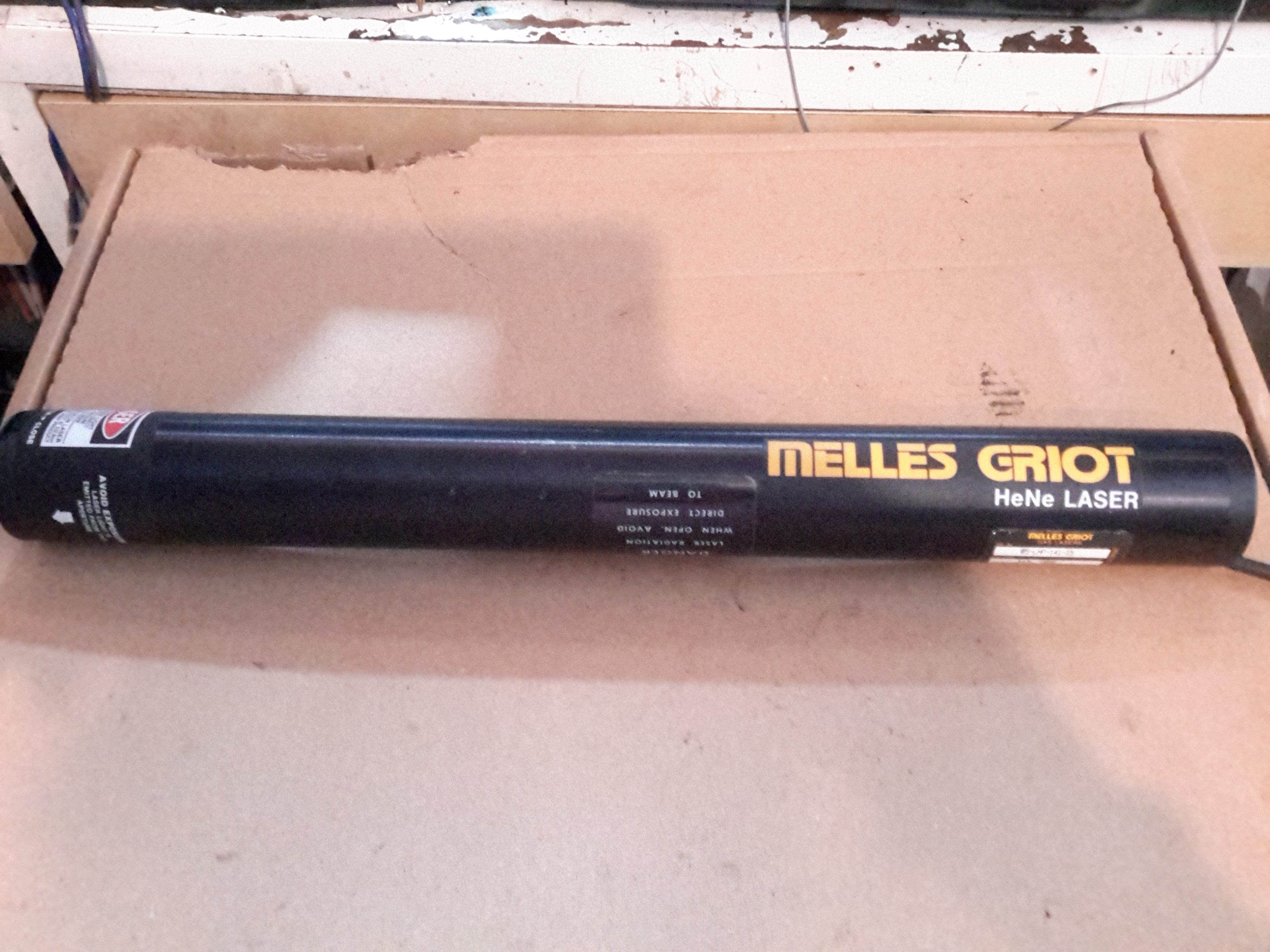
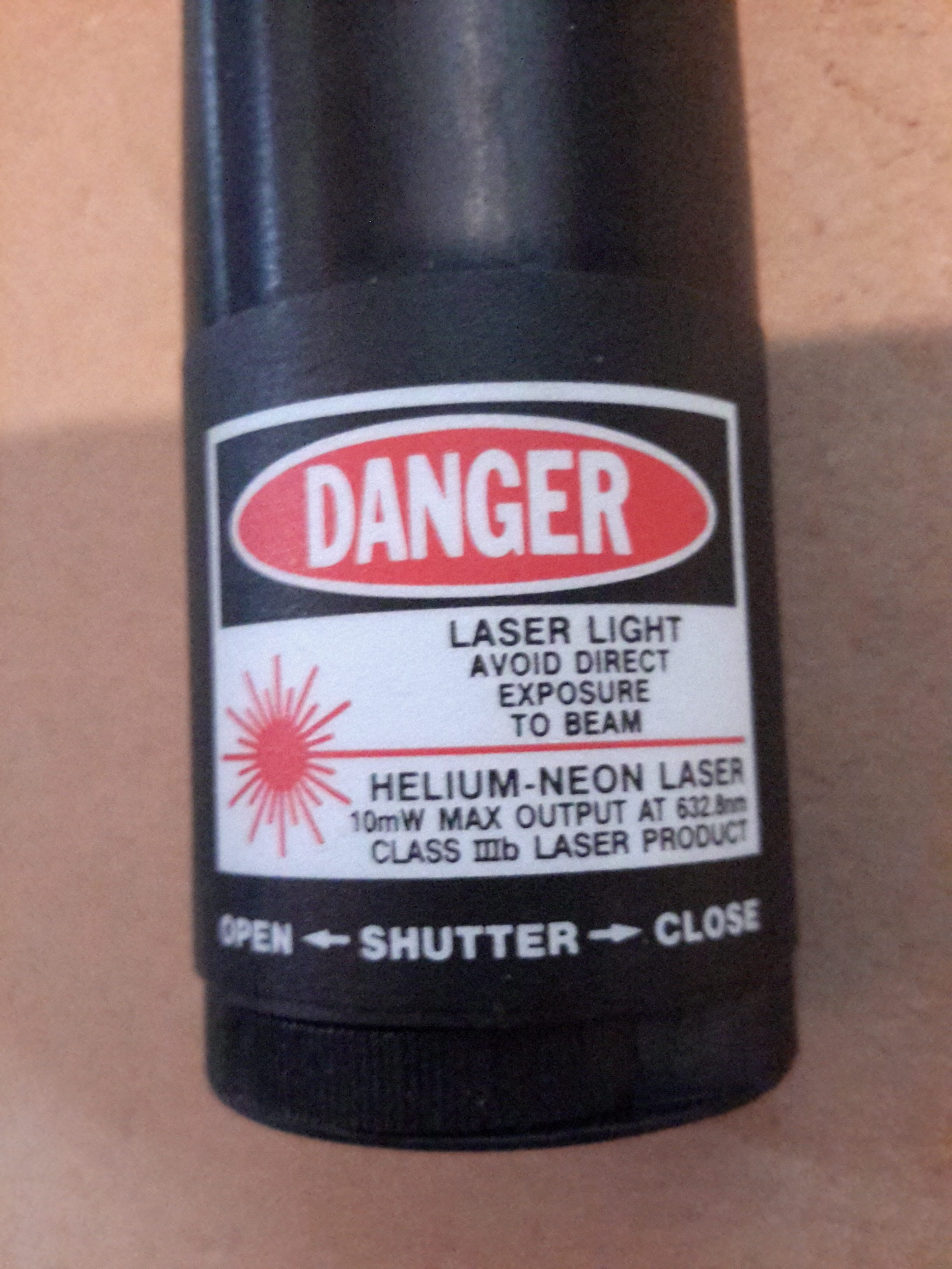
Looking through eBay recently I came across a great deal on some Helium-Neon laser heads from Melles Griot. While definitely not new, these gas lasers are extremely long-lasting & I figured the tubes inside would make a nice addition to my laser collection. Doing some searching on the model number, these heads are rated at an optical output of 4mW, but depending on how much milage is on the tubes, the output may be a bit higher.
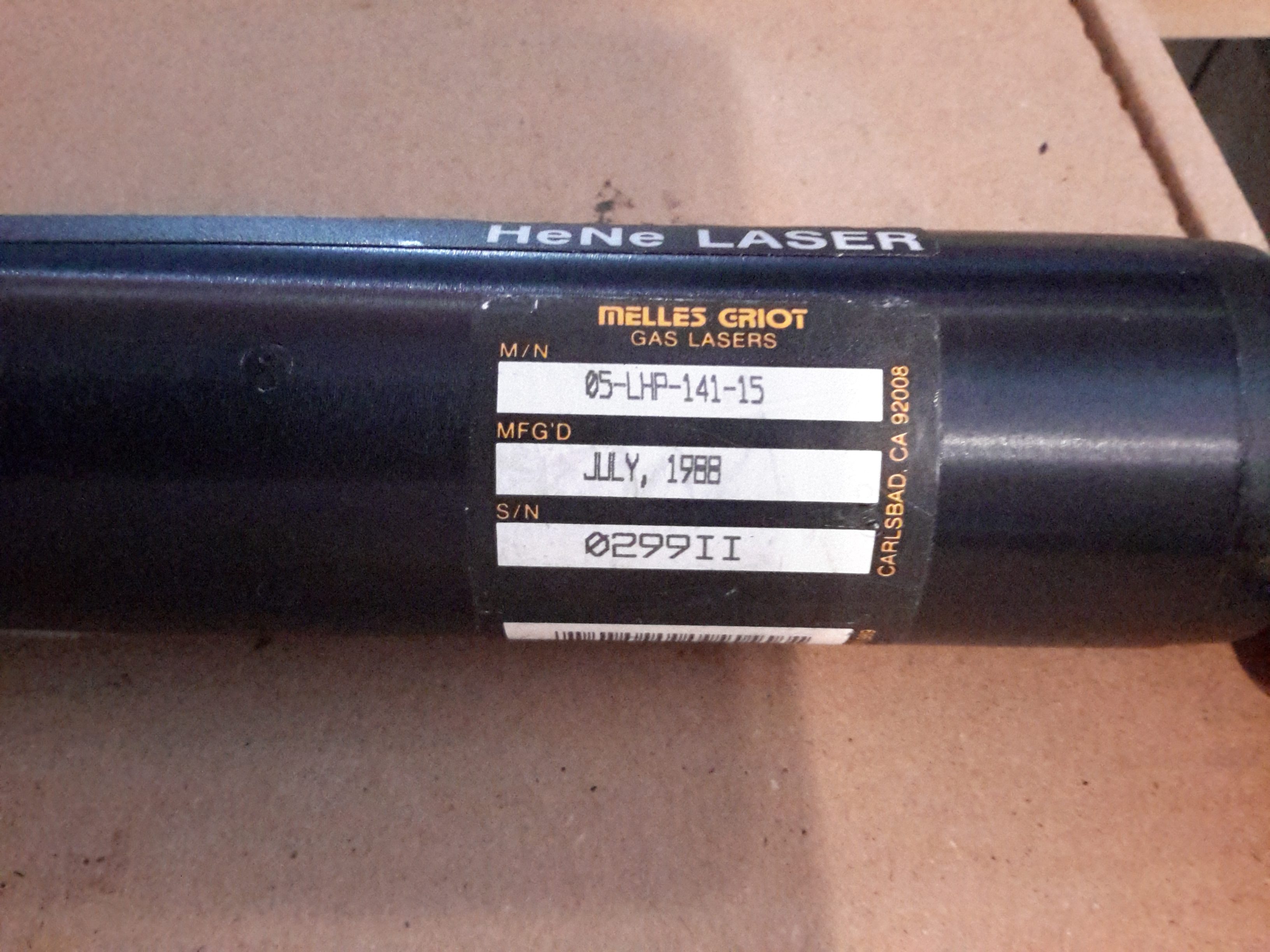
Data Label
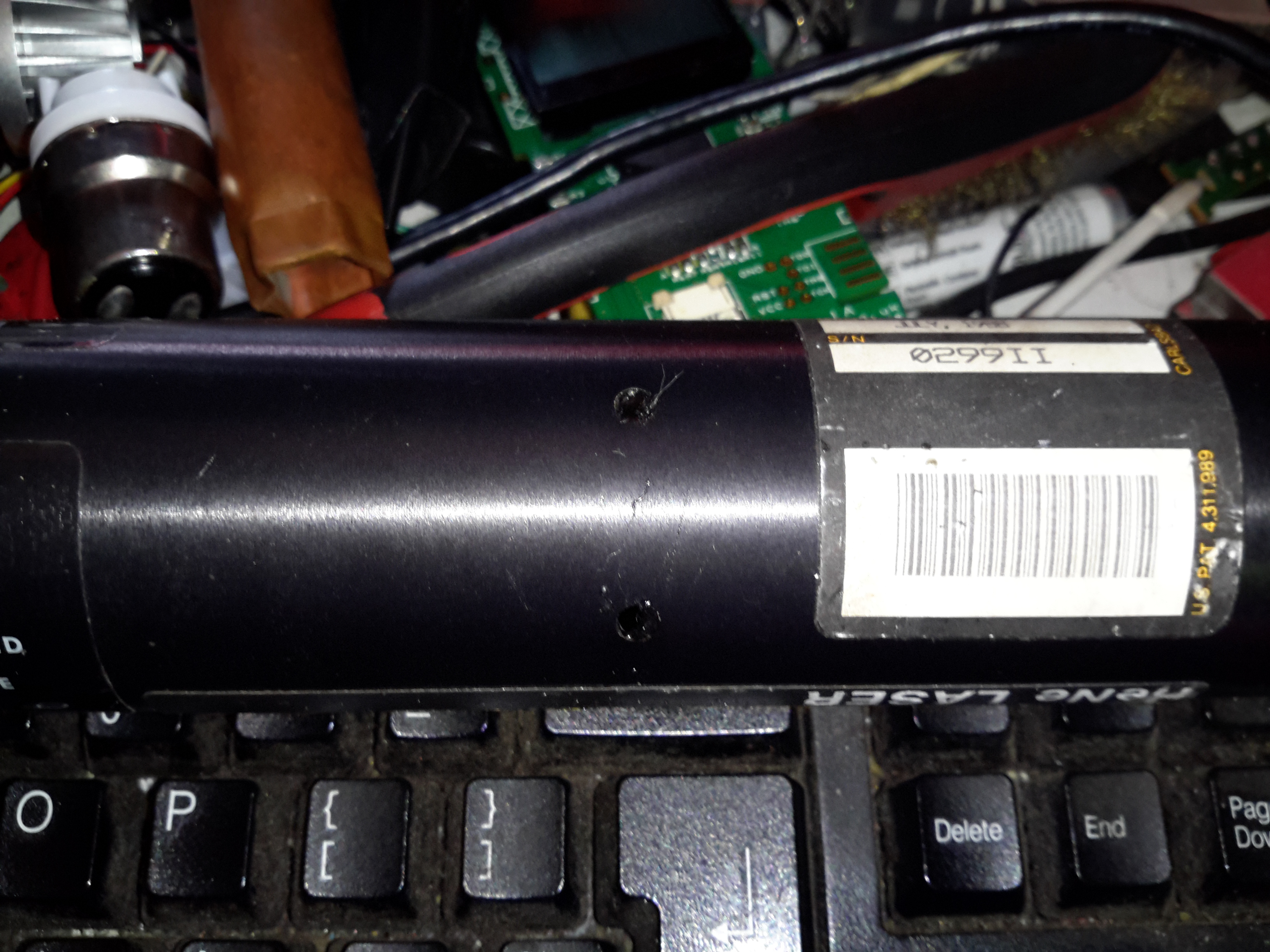
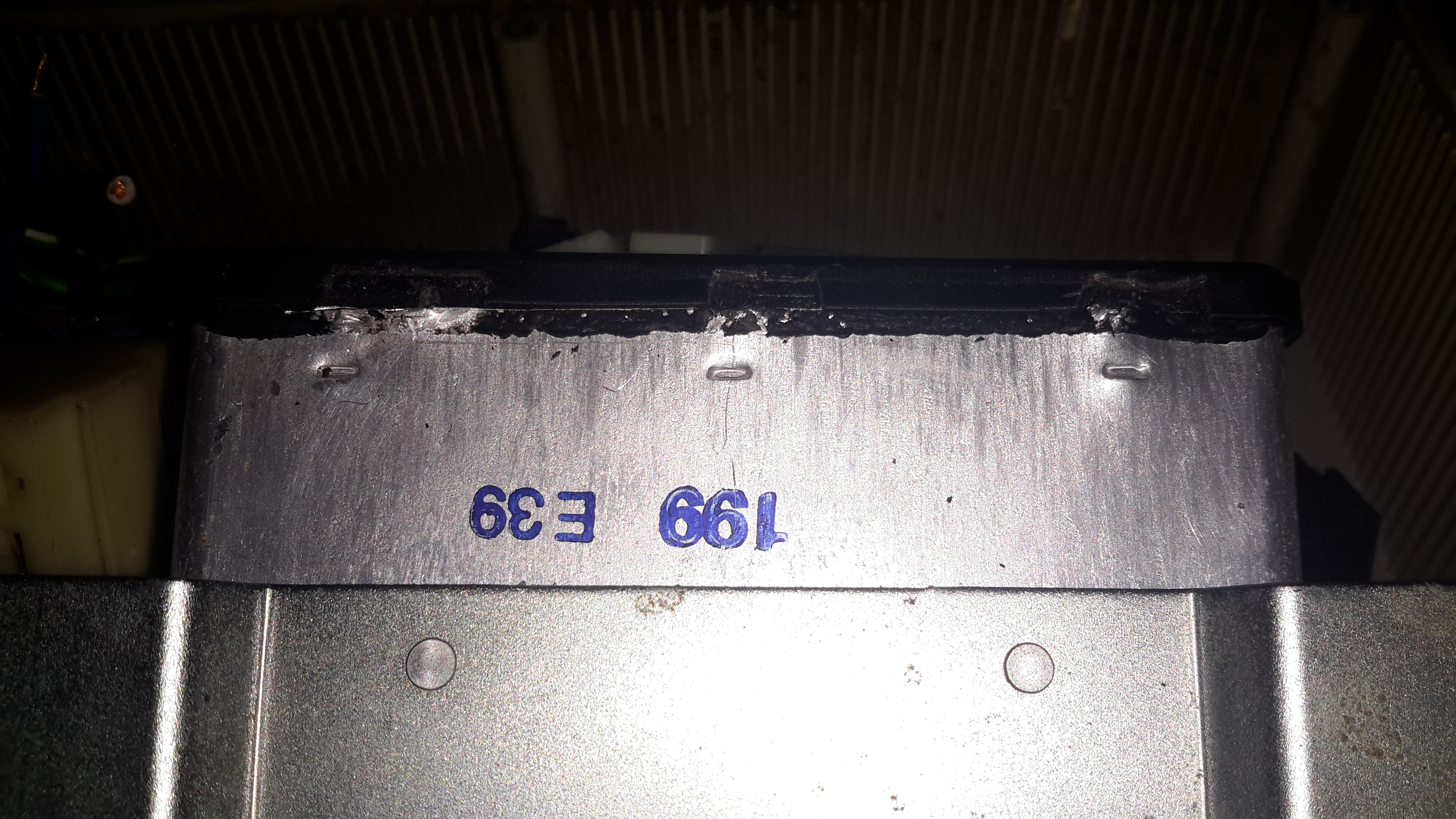
I got a pair of the heads, this one was manufactured in July 1988, the other March 1989.
OC End / Classification Label
The OC end of the head has the laser classification label & the beam shutter. Once I’d tested the laser heads to make sure they survived the post intact, I set at extracting the plasma tubes from the aluminium housings.
The end caps are fibre-reinforced plastic & are secured with epoxy resin, so some heating & brute force released the caps from the housing, giving access to the laser tube itself.
Glue Holes
The laser tube is secured in these heads by hot glue – this was squirted into the housing via two rows of holes around the ends. (Some are secured with RTV silicone, which is substantially more difficult to remove).
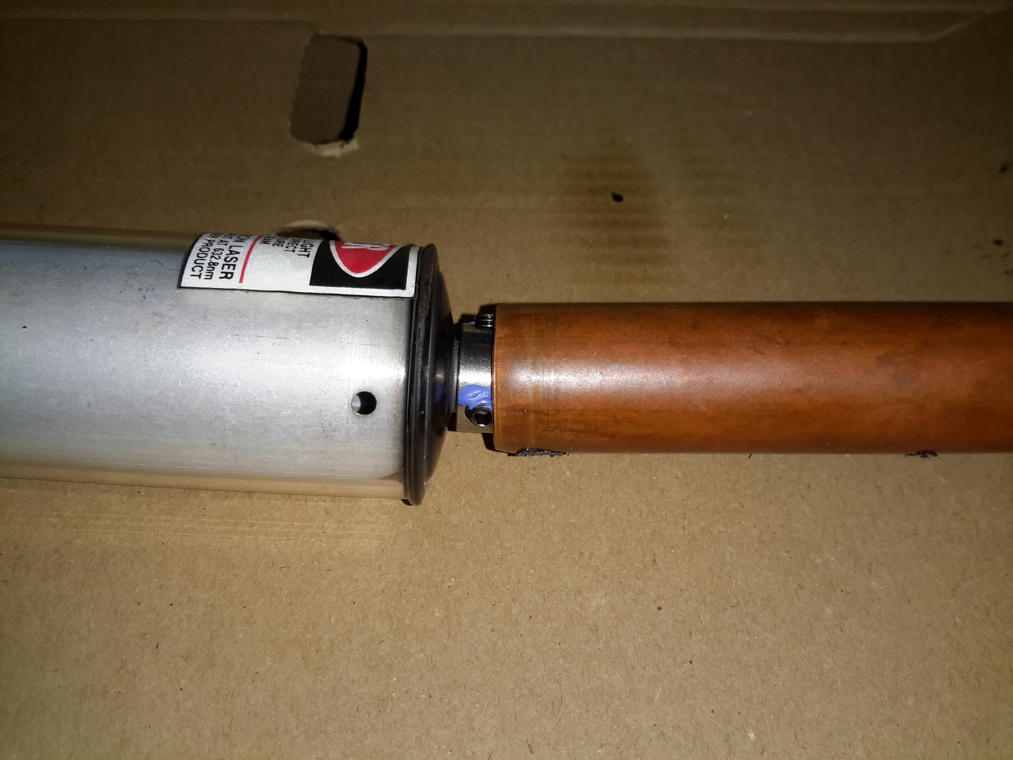
Copper Tube
I’ve no photos of the actual extraction process as it’s difficult enough as is without at least 5 hands. A heat gun was used to warm up the housing until the glue melted enough to slide the tube out of the housing. Since everything was hot at this stage, a piece of copper tubing (above), was slipped over the OC mirror mount, so I could push the tube out of the housing while the glue was soft. This also protected the mirror from damage while the tube was being removed.
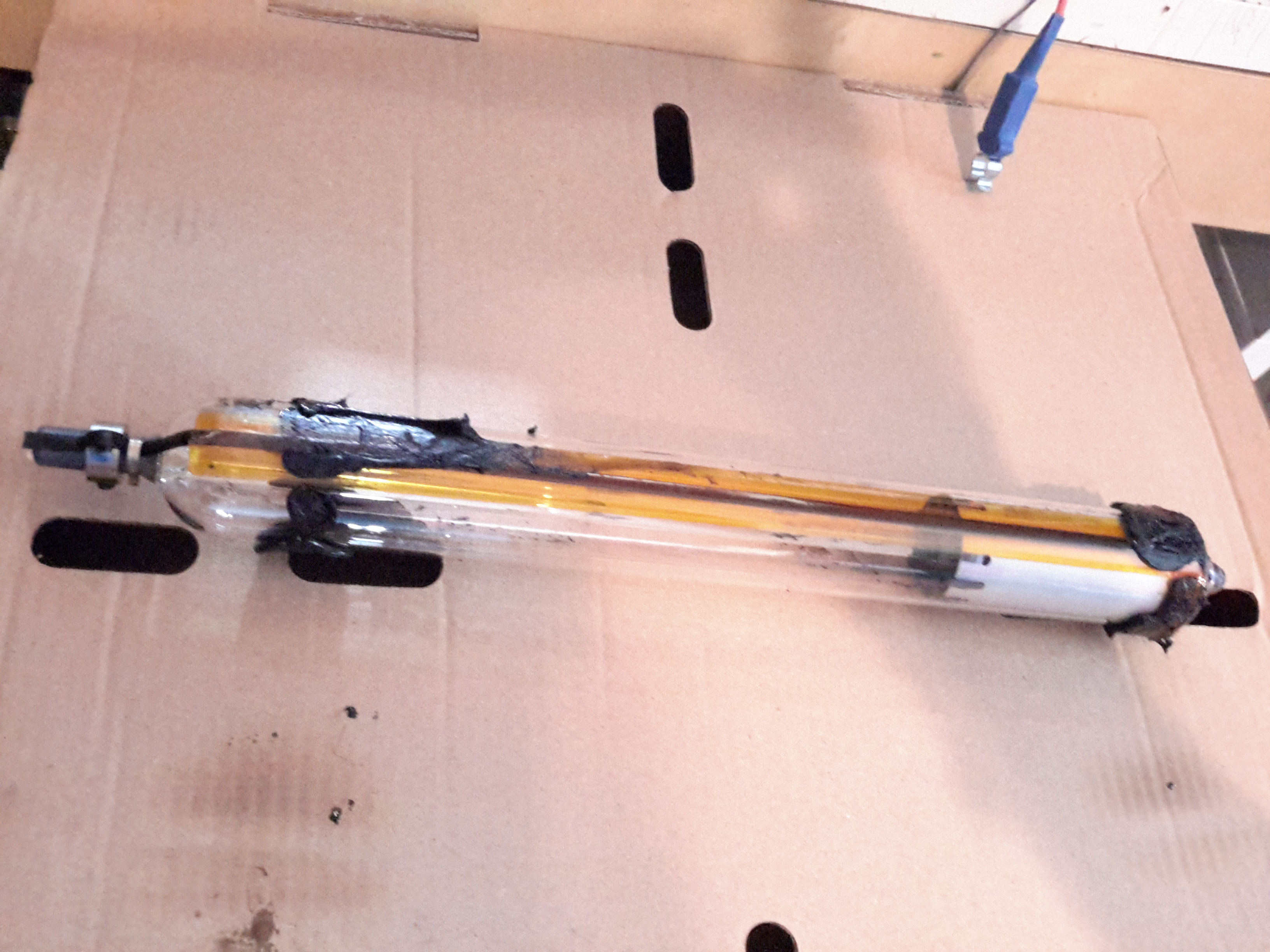
Extracted Tube
After a few minutes of gentle pushing while keeping the housing hot, the tube was released! It’s still pretty well covered in the remains of the hot glue, but this is easily removed once the tube cools down to room temperature with Isopropanol. The line of Kapton tape running down the tube to the cathode end is insulating a start tape electrode, which is supposed to make the laser strike faster on power-up. Instead of being metal though, the electrode appears to be a carbon-loaded plastic tape.
Start Tape & Adhesive
Here’s the HR end of the tube, which also serves as the high voltage anode electrode. The start tape is clipped onto the mirror mount, but all this will be removed.
OC End
The OC end of the laser, where the beam emerges. What I think is the mW rating of the tubes is written on the end cap, probably from when the tubes were manufactured.
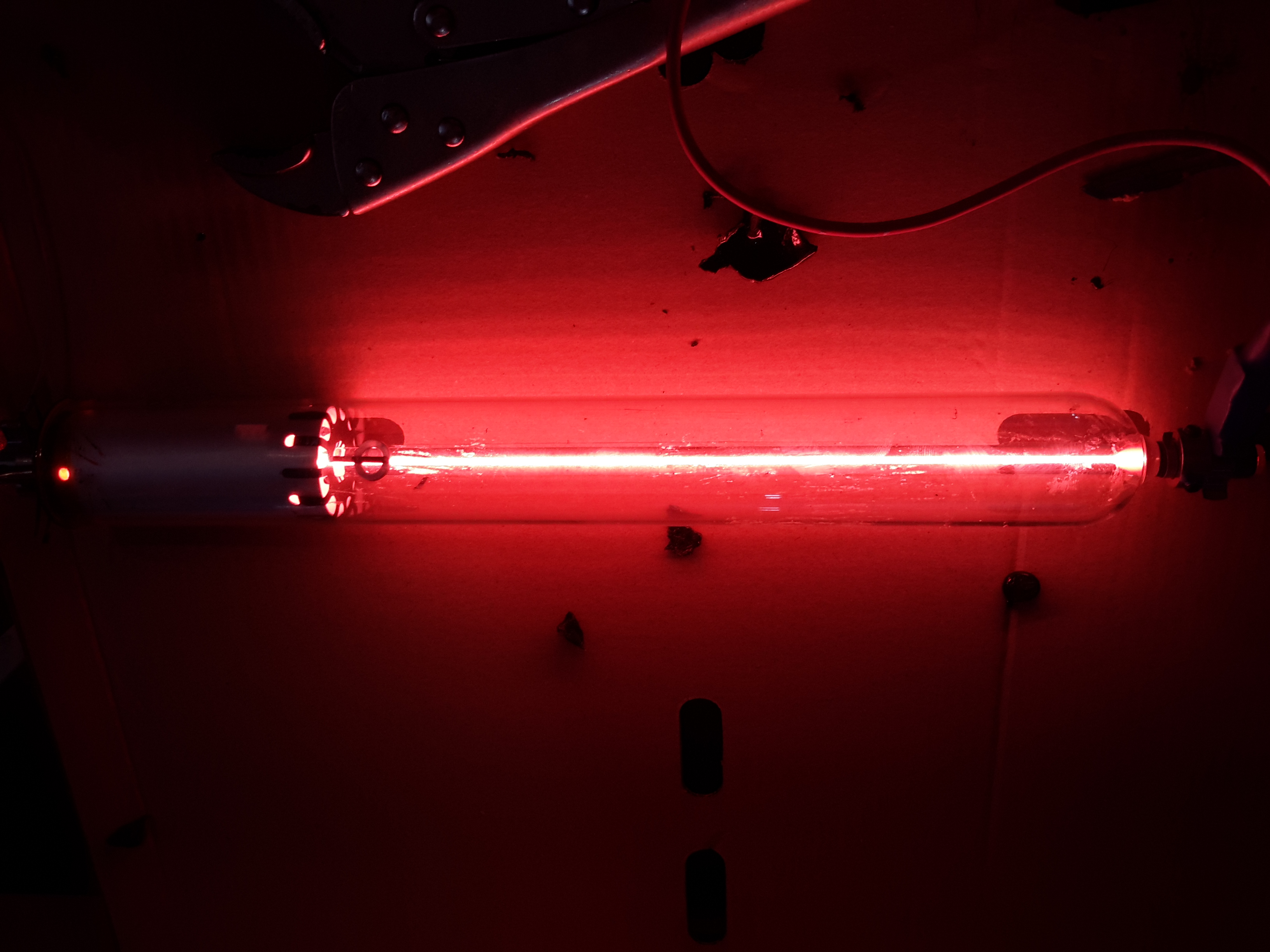
Tube Energized
Applying power from a He-Ne laser PSU confirmed the tube still works!
Another random teardown from the junk box time!
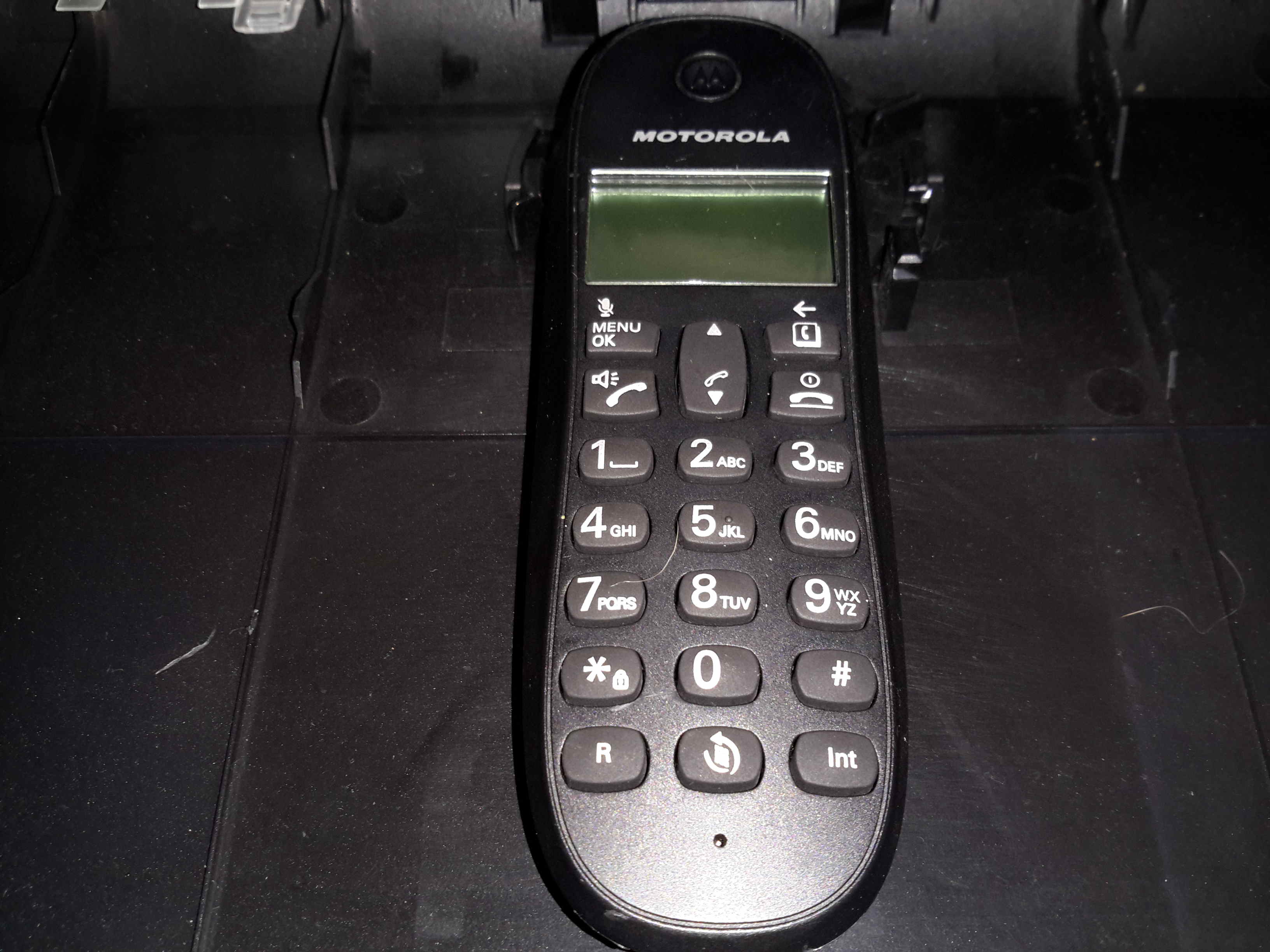
Here’s an old Motorola DECT landline phone, no use to me as I’ve not used a landline for many years.
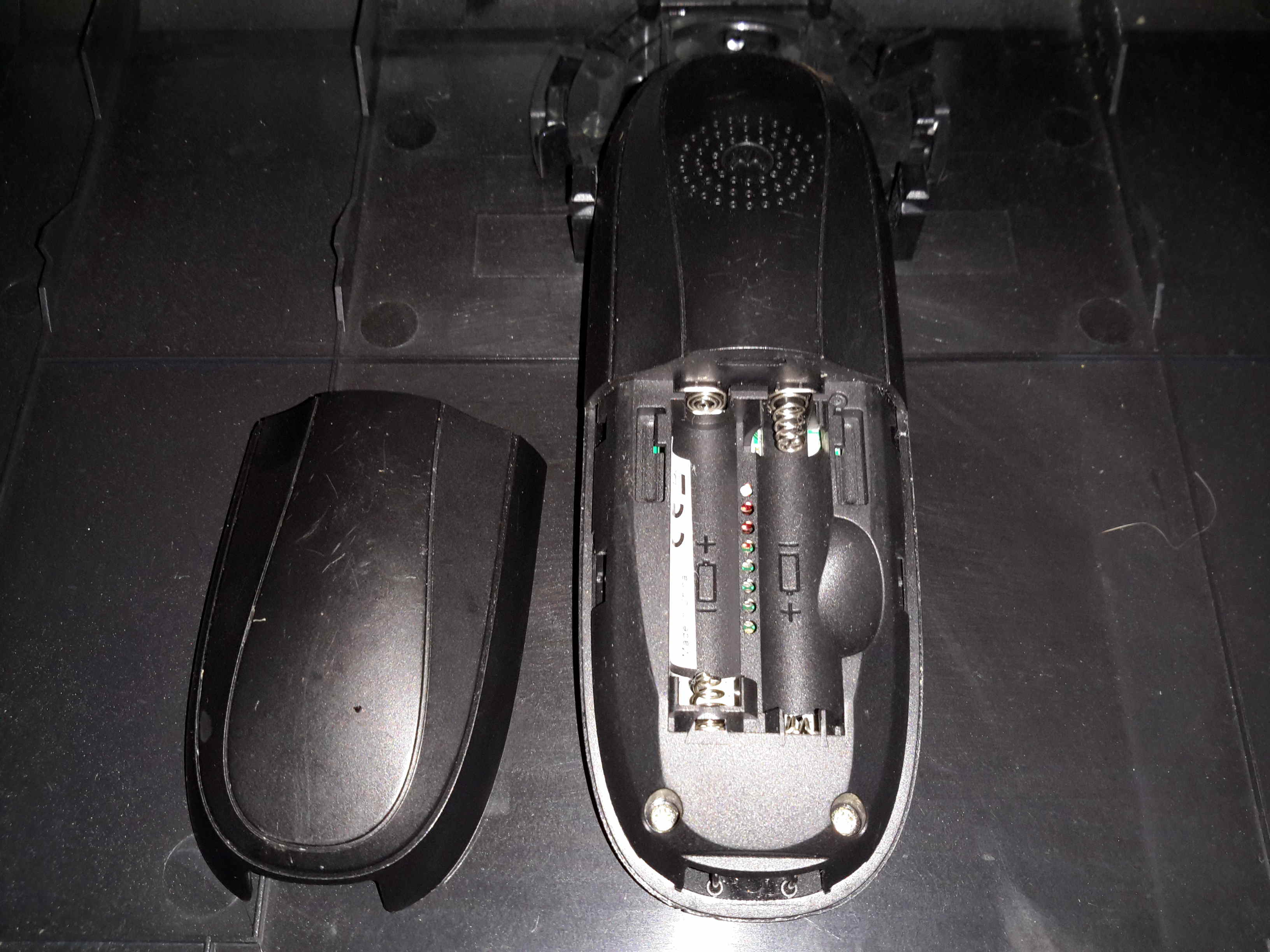
Battery Compartment
Not much on the back, other than the battery compartment for a pair of AAA rechargables. The base unit contains the charger.
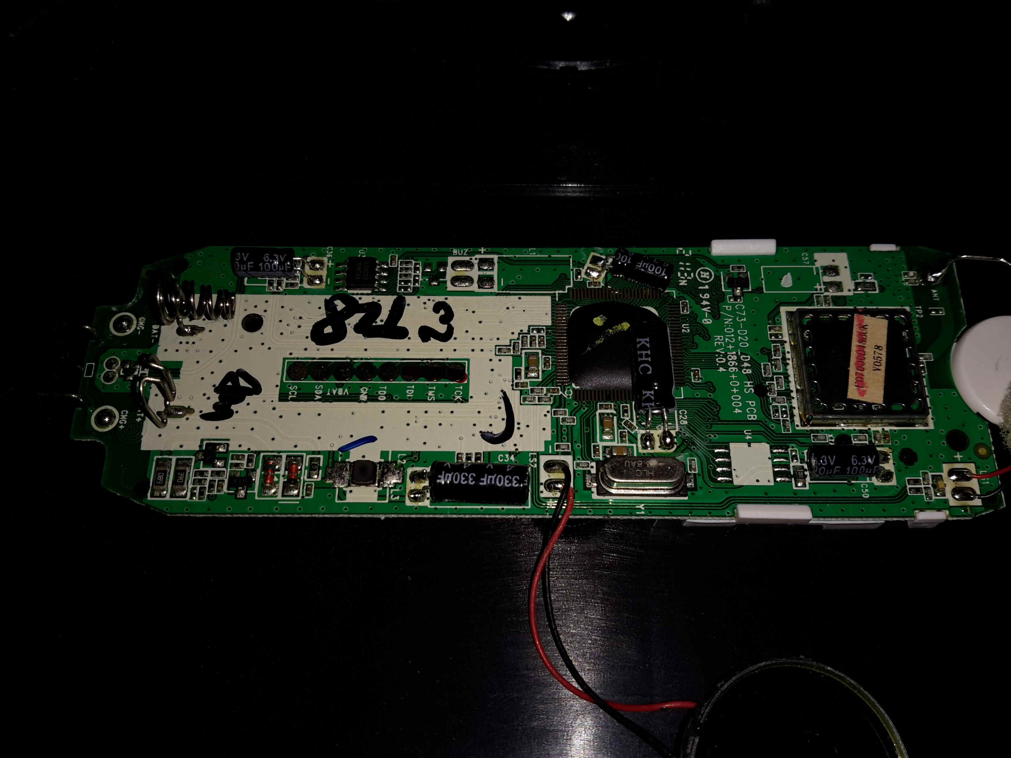
Main PCB
Here’s the main PCB removed from it’s casing. There’s not really much going on, one of the main ICs, which is probably a microcontroller, is a COB device, so no part numbers from there. There’s a row of pads for programming the device at the factory. The RF section is on a dedicated IC, a DE19RF19ZCNC from DSP Group. I couldn’t find much on this part, but it’s one of a range of DECT/VoIP DSP devices.
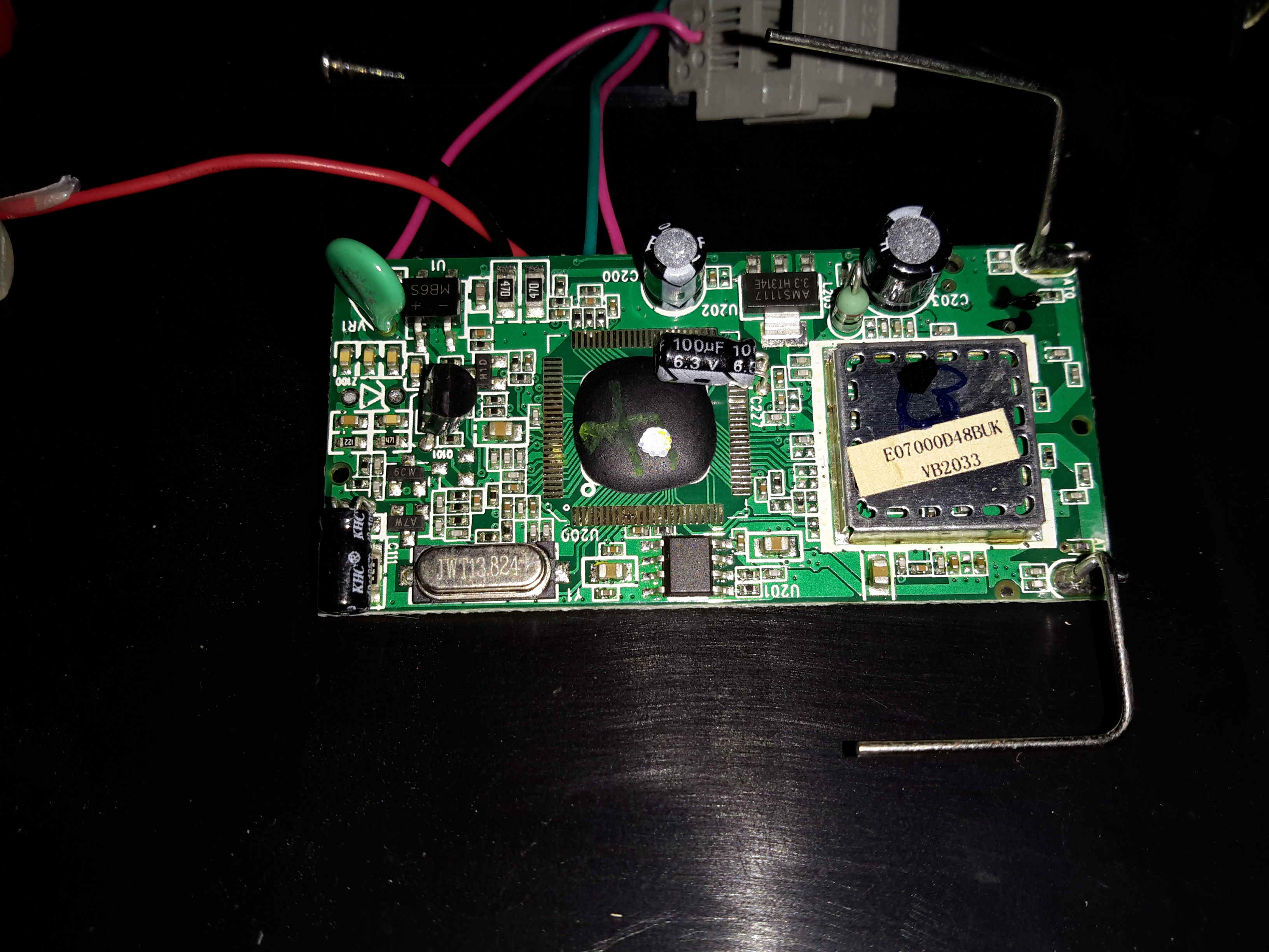
Base Unit PCB
Inside the base unit is a similar board, just without the keypad. Main microcontroller is again a COB device, the RF IC is under the shield.
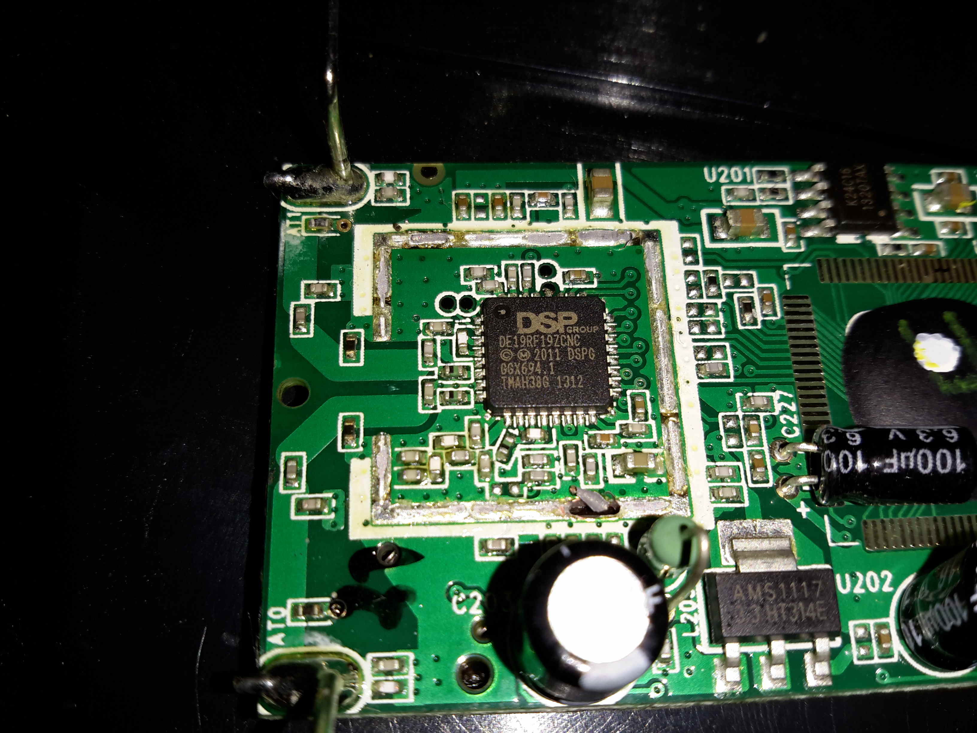
Main Chipset
Removing the shield reveals the same IC as in the handset, only this PCB has a pair of antennas.
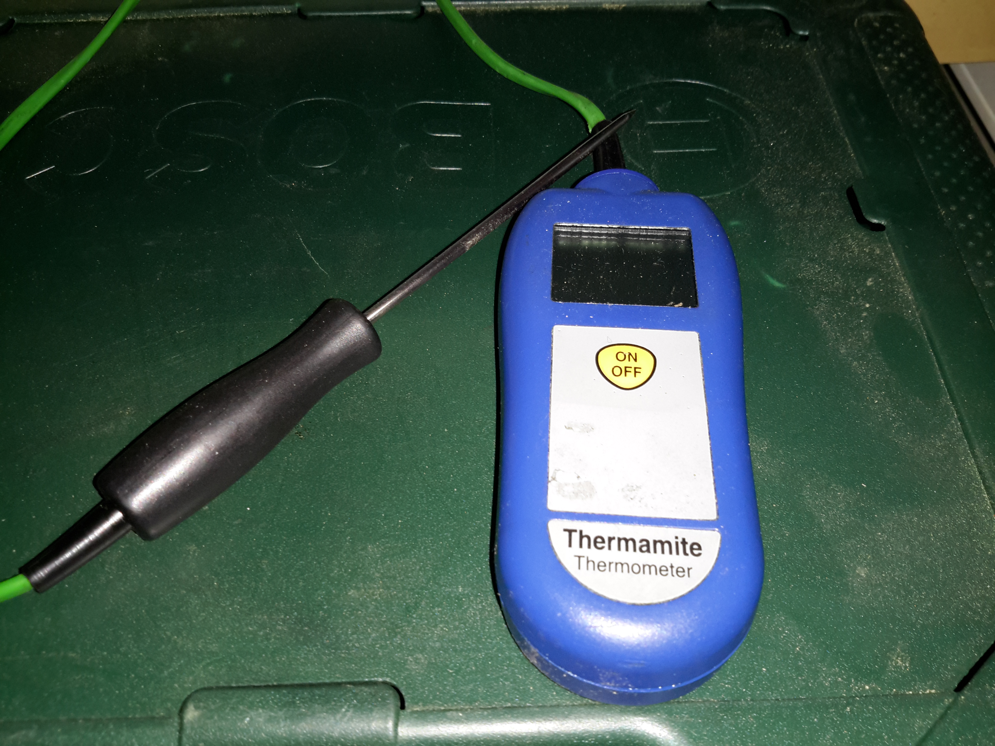
Here’s another bit of commercial gear, a catering thermometer. These are used to check the internal temperature of foods such as meat, to ensure they’re cooked through.
This was given to me with some damage, the battery cover is missing & the plastic casing itself is cracked.
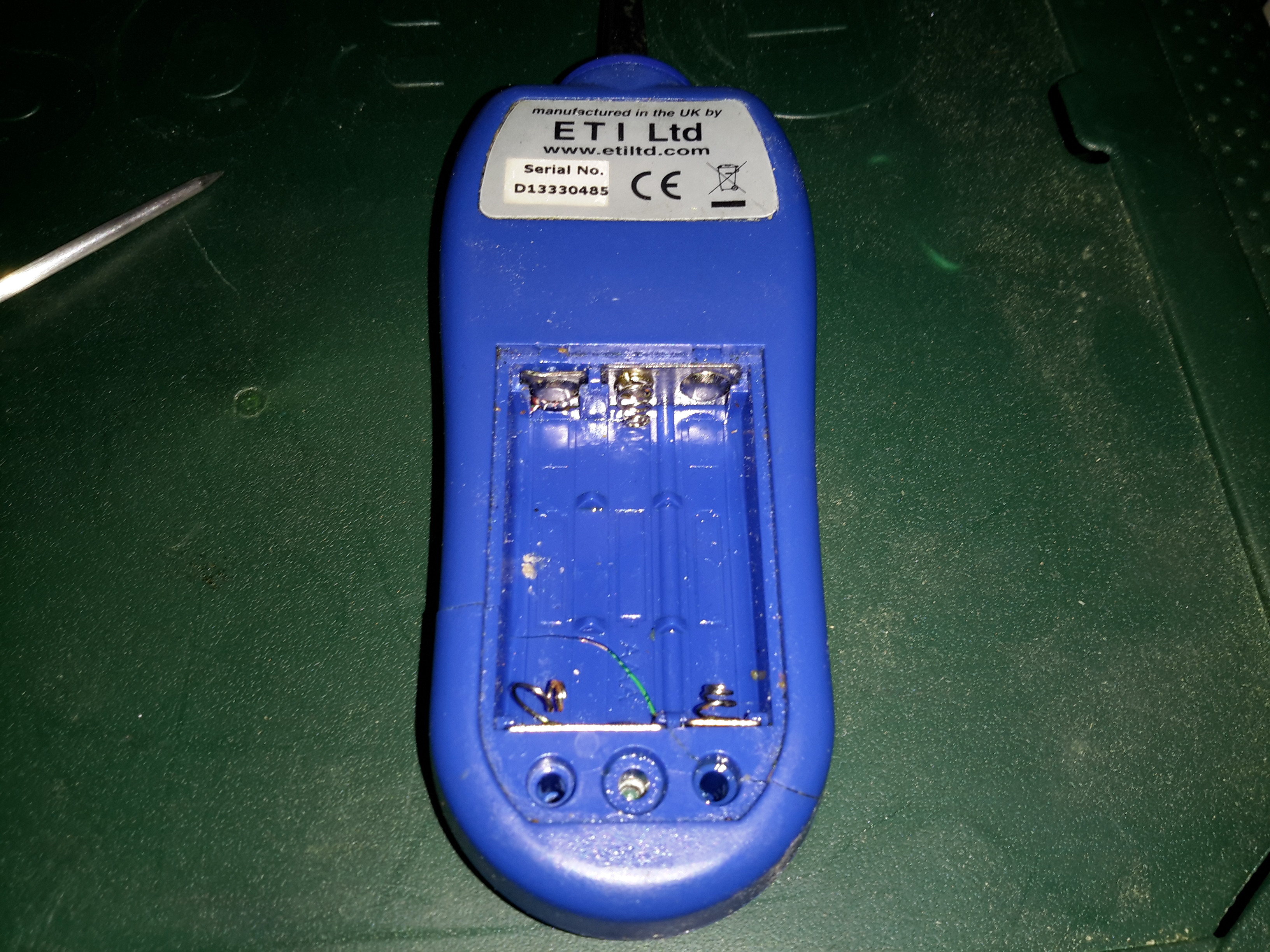
Battery Compartment
Power is provided by 3 AAA cells, for 4.5v
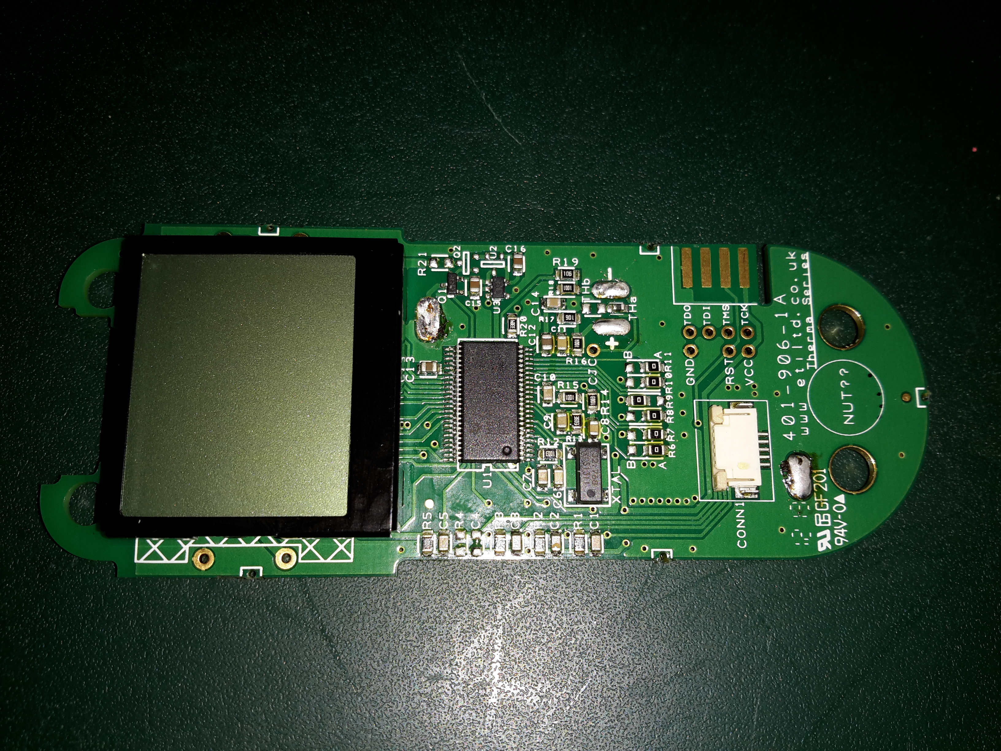
Main PCB
There’s not much to these units, the large LCD at the top is driven by the IC in the centre. A programming header is also present on the board near the edge.
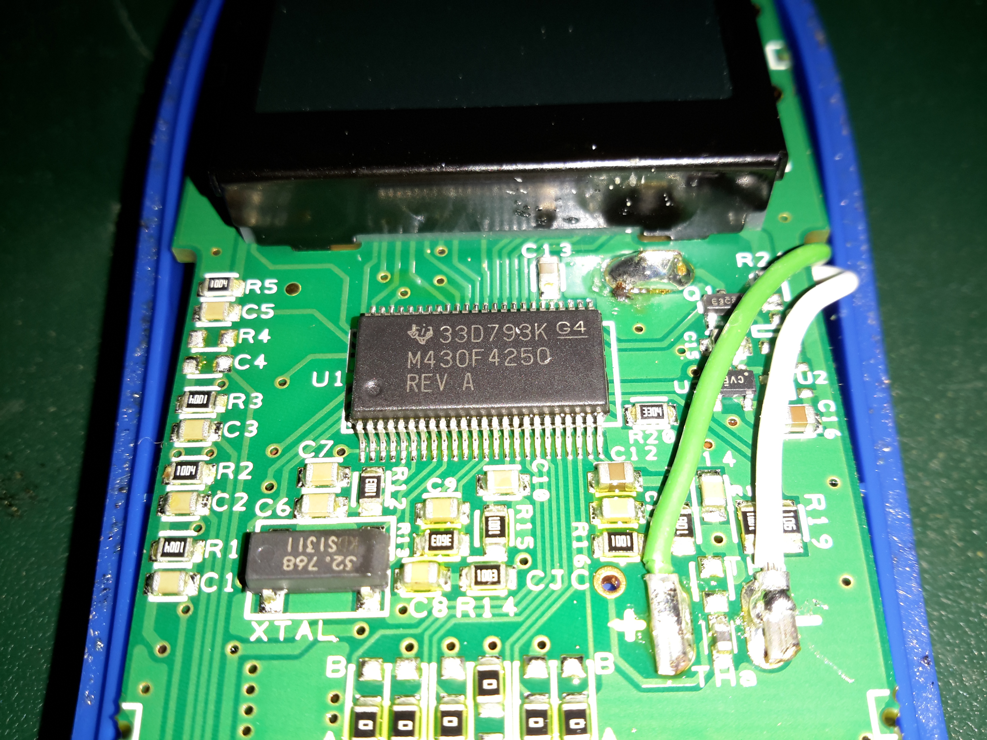
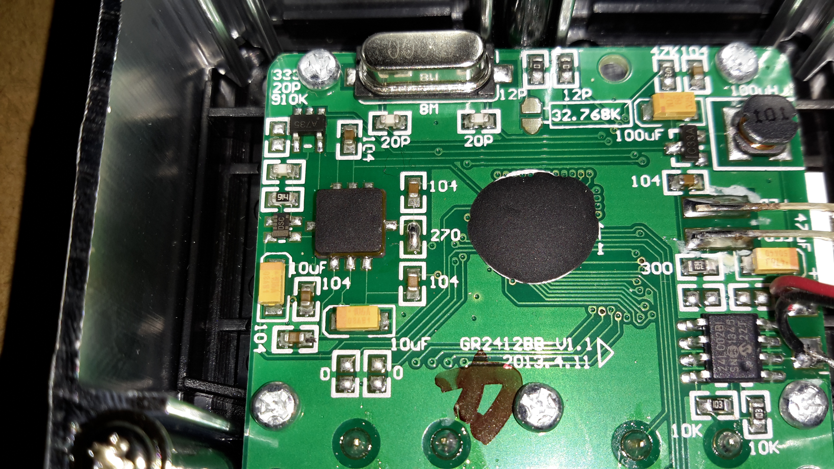
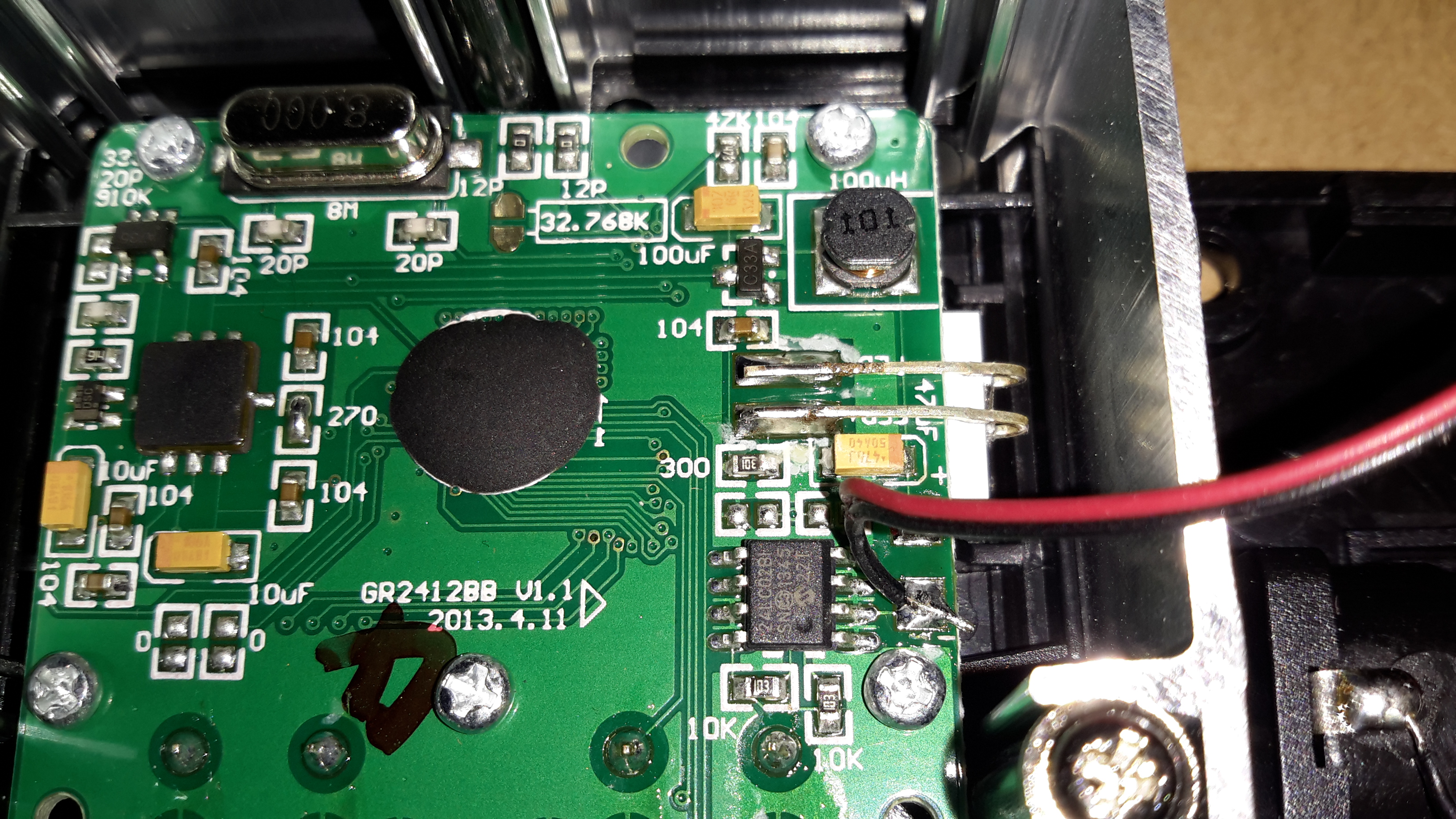
Microcontroller
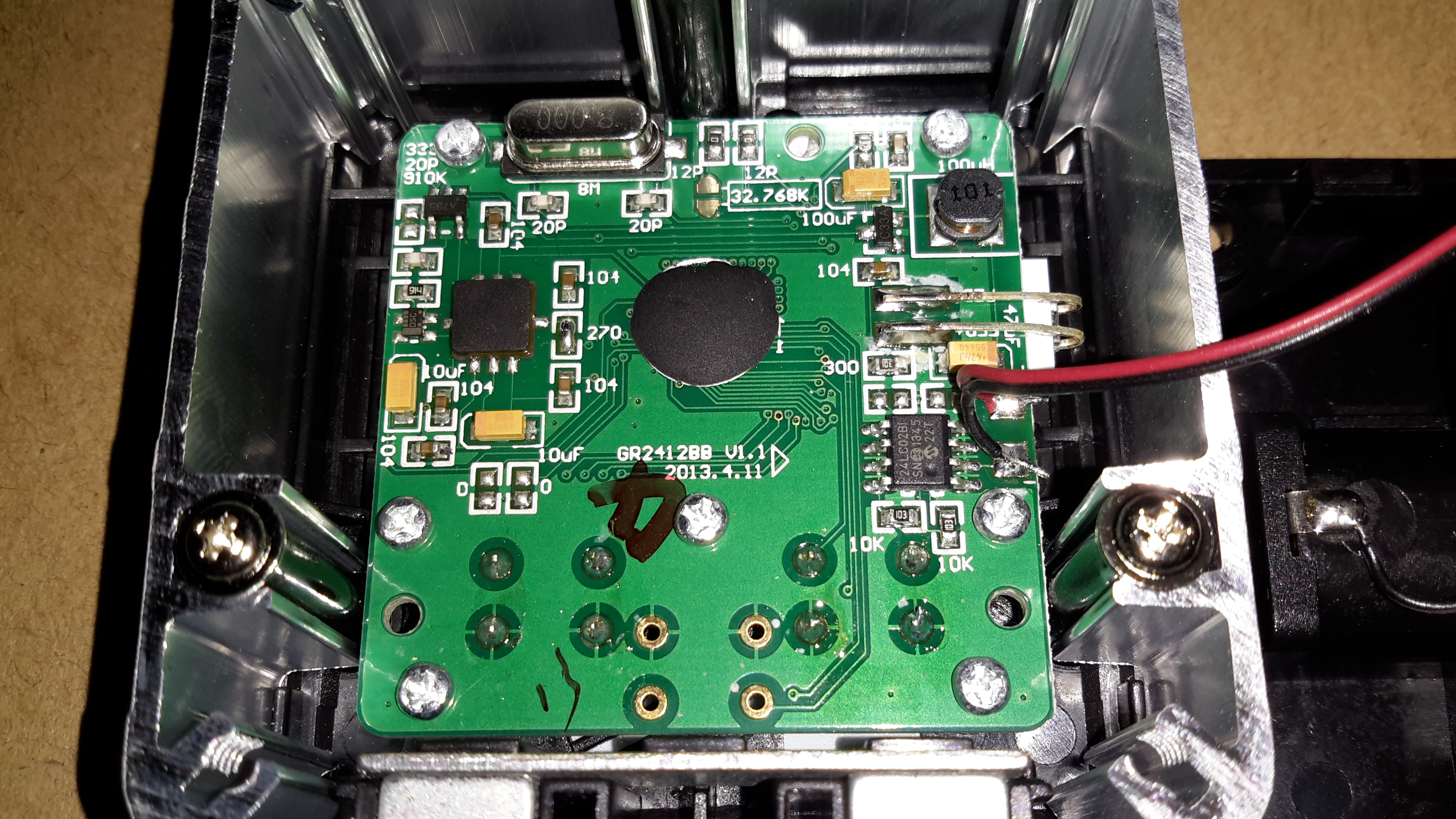
The core logic is taken care of with a Texas Instruments M430F4250 MSP430 Mixed-Signal Microcontroller. This MCU has onboard 16-bit Sigma-Delta A/D converter, 16-bit D/A converter & LCD driver. Clock is provided by a 32.768kHz crystal.
The probe itself is just a simple thermistor bonded into a stainless steel rod.
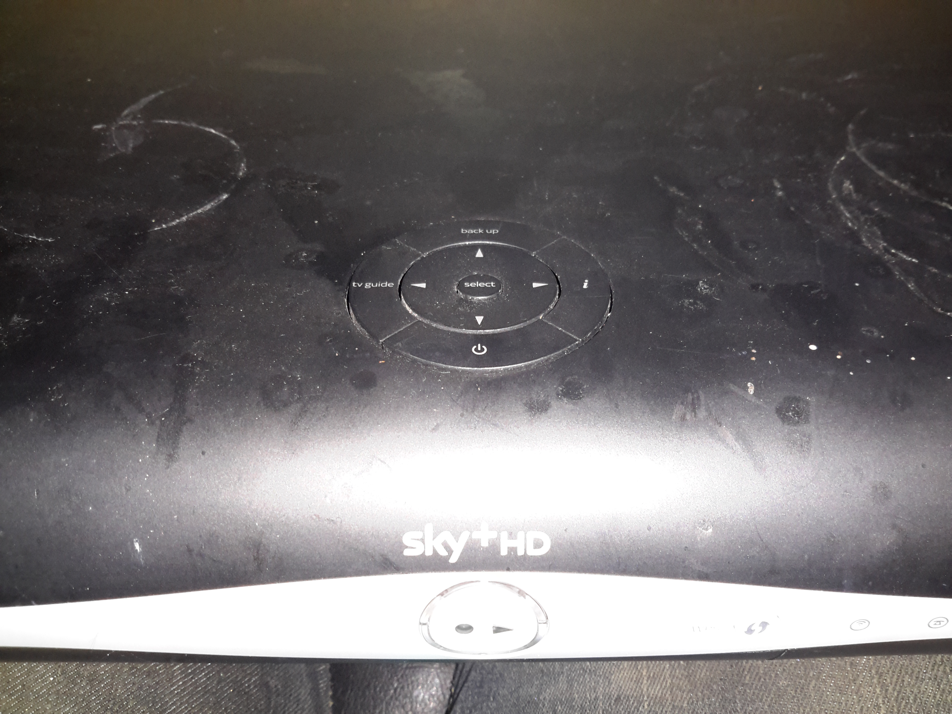
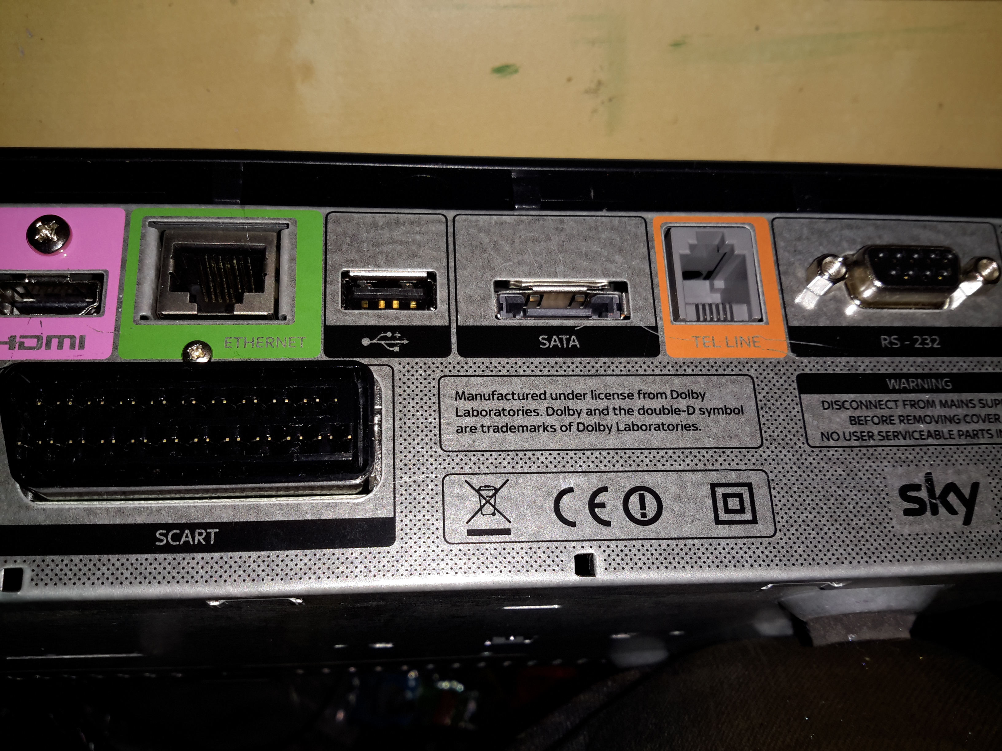
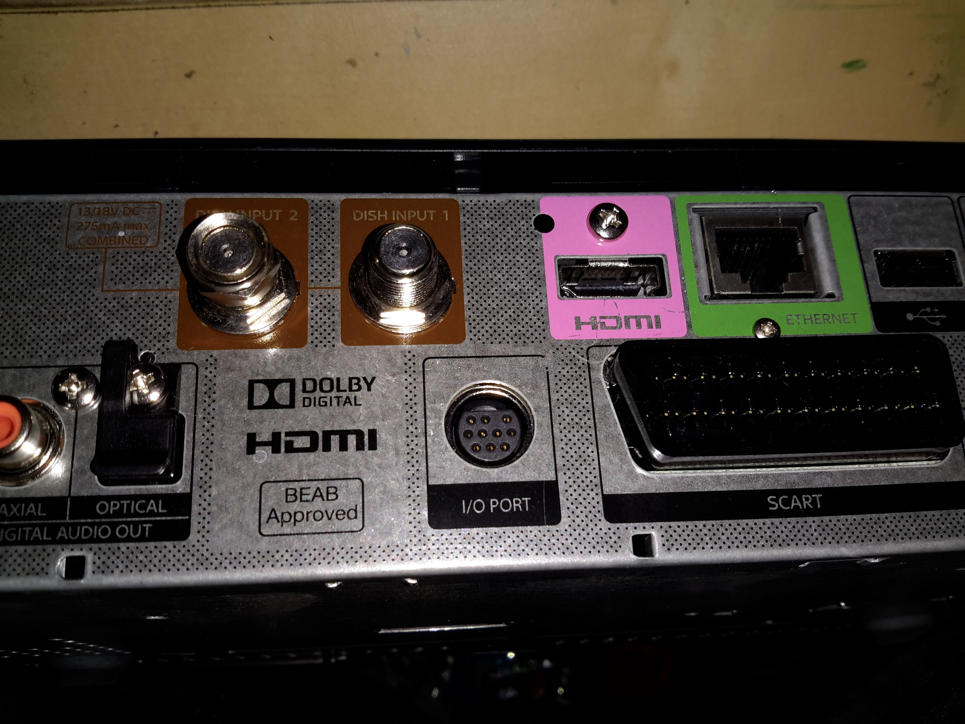
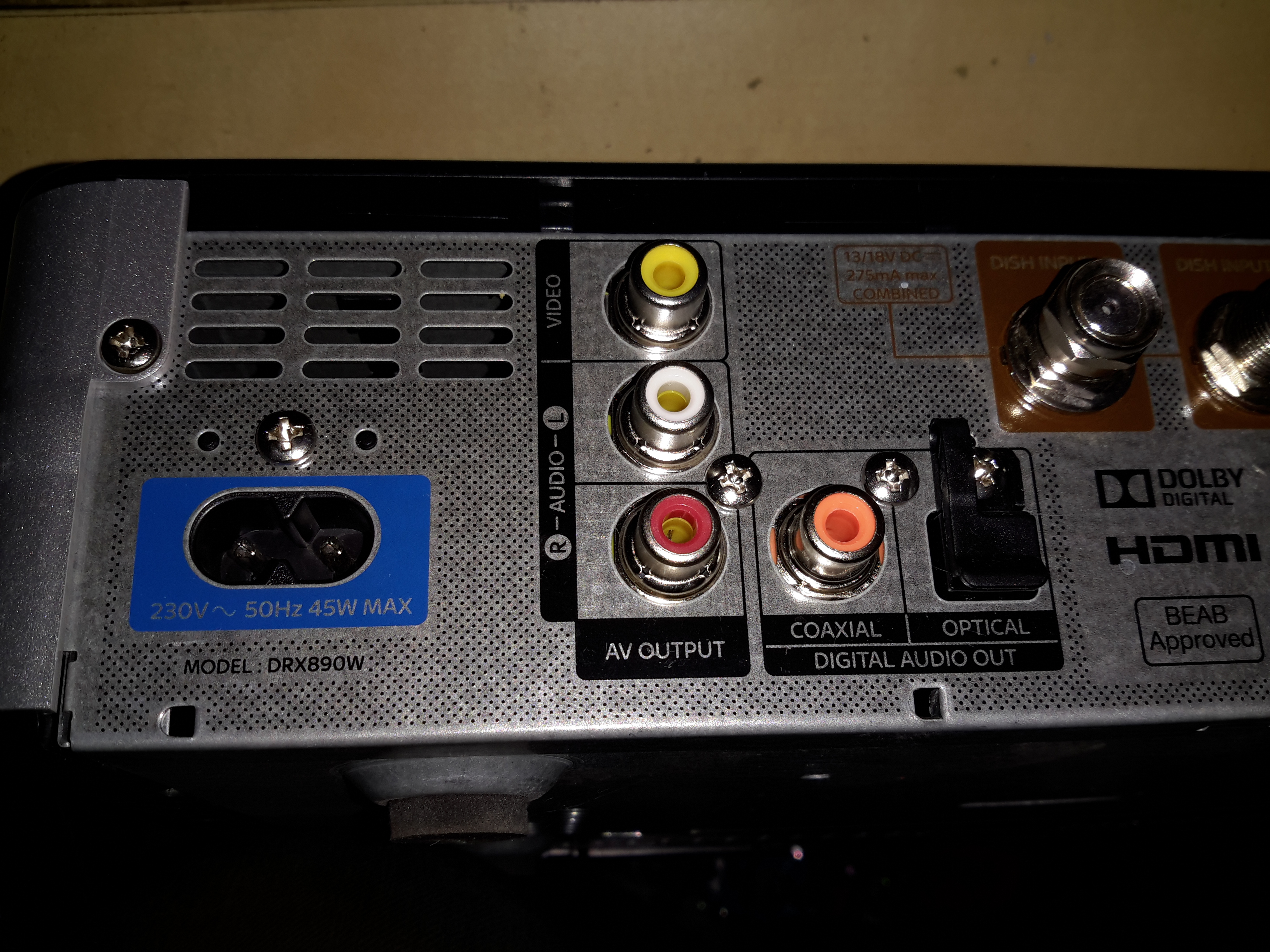
Time for another teardown! I managed to fish this Sky+ box out of a skip, but to protect the guilty, all serial numbers have been removed.
These are pretty smart devices, with DVR capability on board.
Ports 1
There’s a lot of ports on these units, from RS-232 serial, POTS modem, eSATA, HDMI, USB, Ethernet, SCART, Optical, digital outputs & even composite video.
Ports 2Ports 3Top Panel
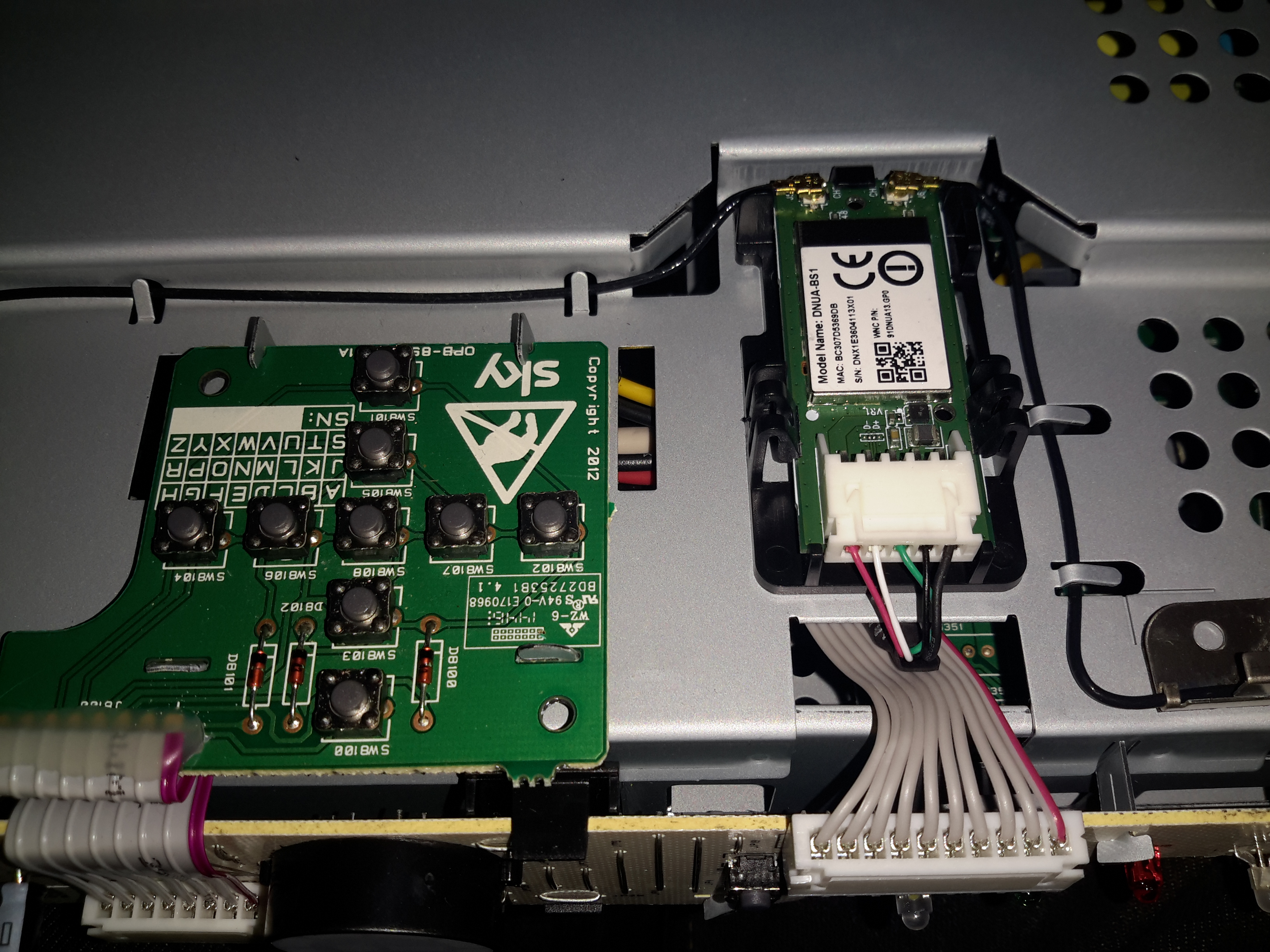
Removing the top plastic cover reveals the operation buttons & the built in WiFi adaptor, which is USB connected to the main logic board.
Front Panel
The PCB on the front of the chassis has all the indicators, and the IR Receiver for the remote.
Cover Removed
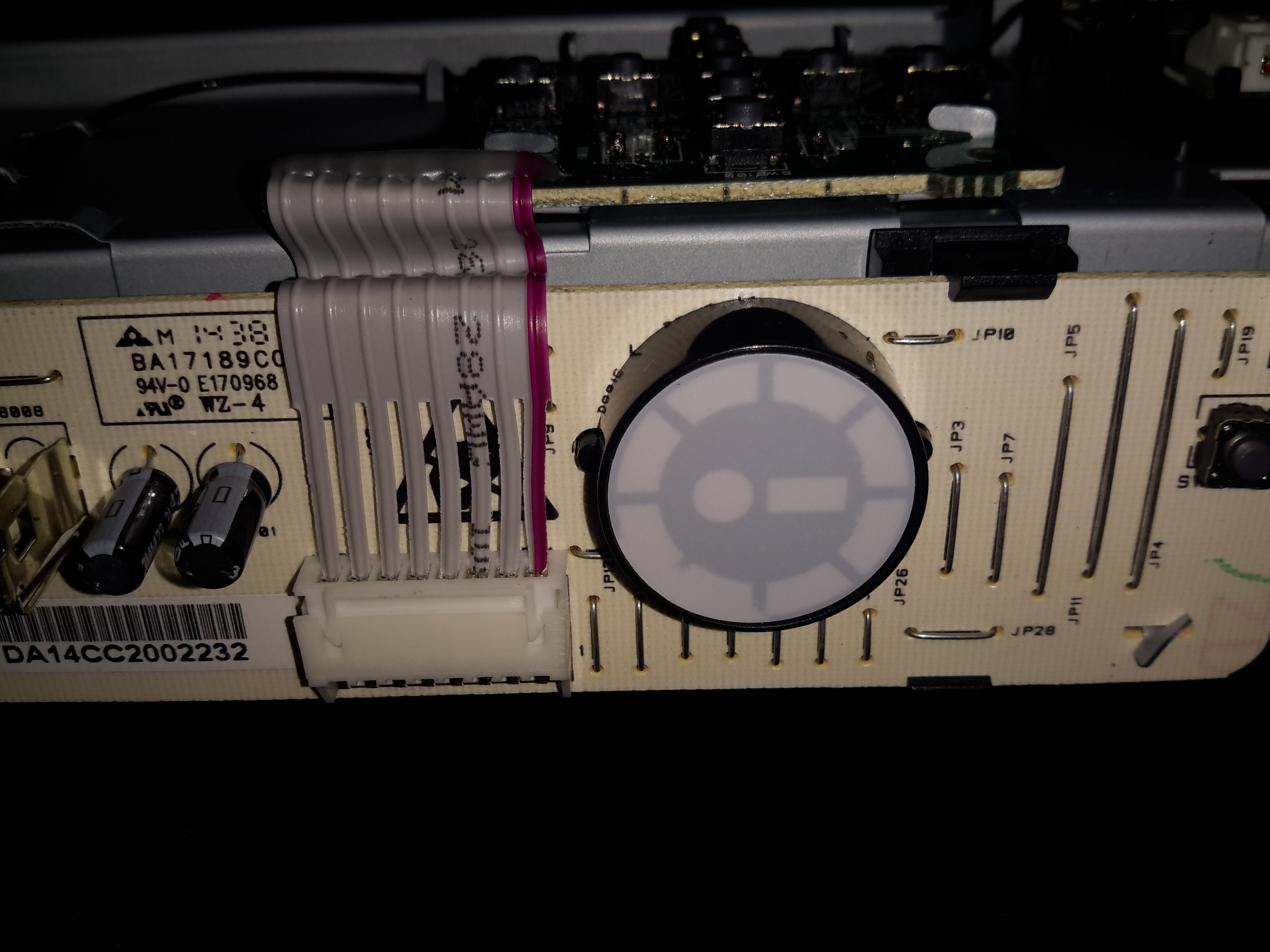
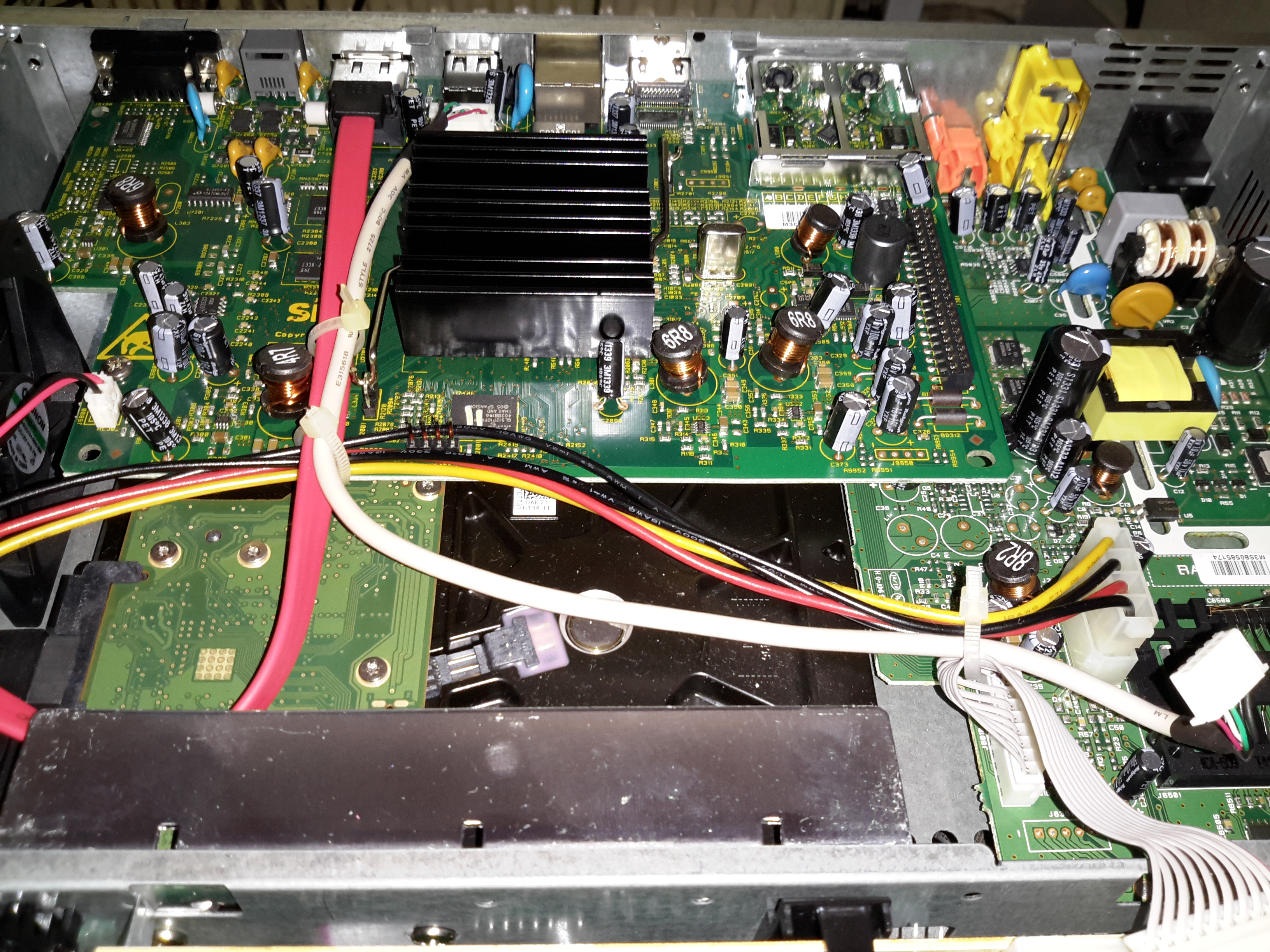
Removing the top shield of the chassis reveals the innards. The PSU is on the top right, 500GB SATA disk drive in the bottom centre. The main logic PCB is top centre.
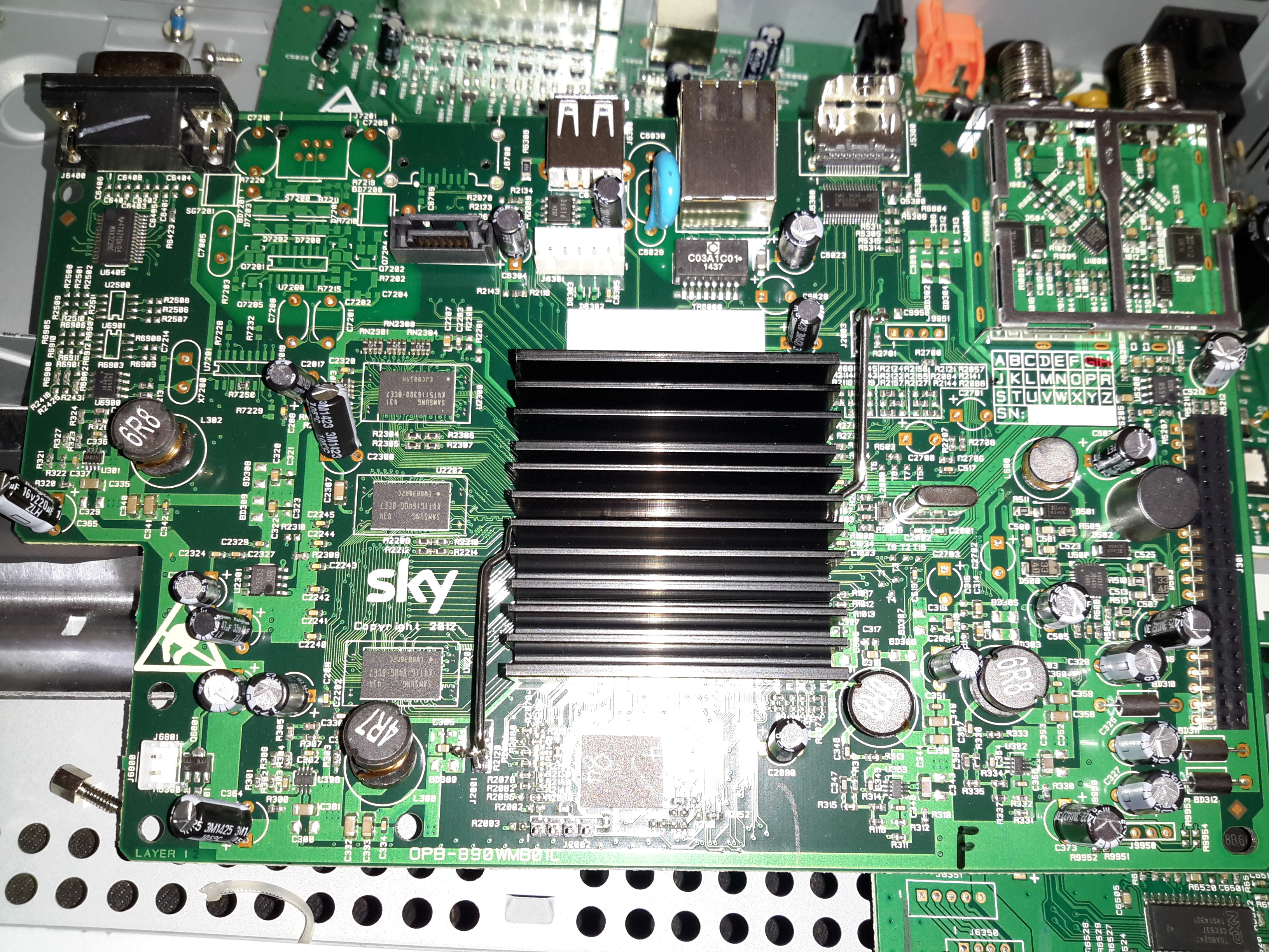
Logic PCB
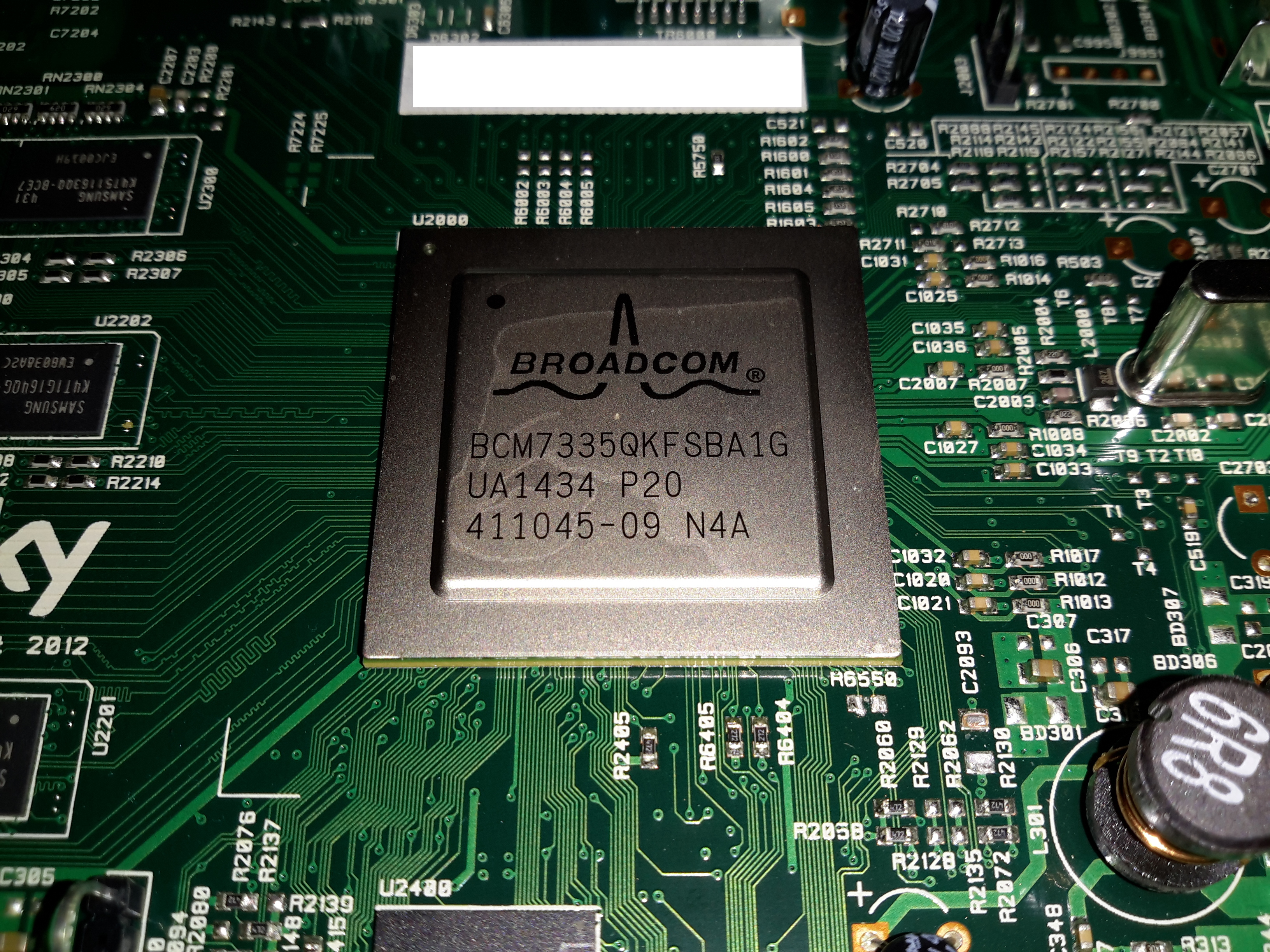
Here’s the main logic PCB. The massive heatsink in the middle is cooling the main SoC, below.
SoC
The main SoC in this unit is a Broadcom BCM7335 HD PVR Satellite System-On-Chip. It’s surrounded by it’s boot flash, a Spansion GL512P10FFCR1 512Mbit NOR device. It’s also got some DRAM around the left edge.
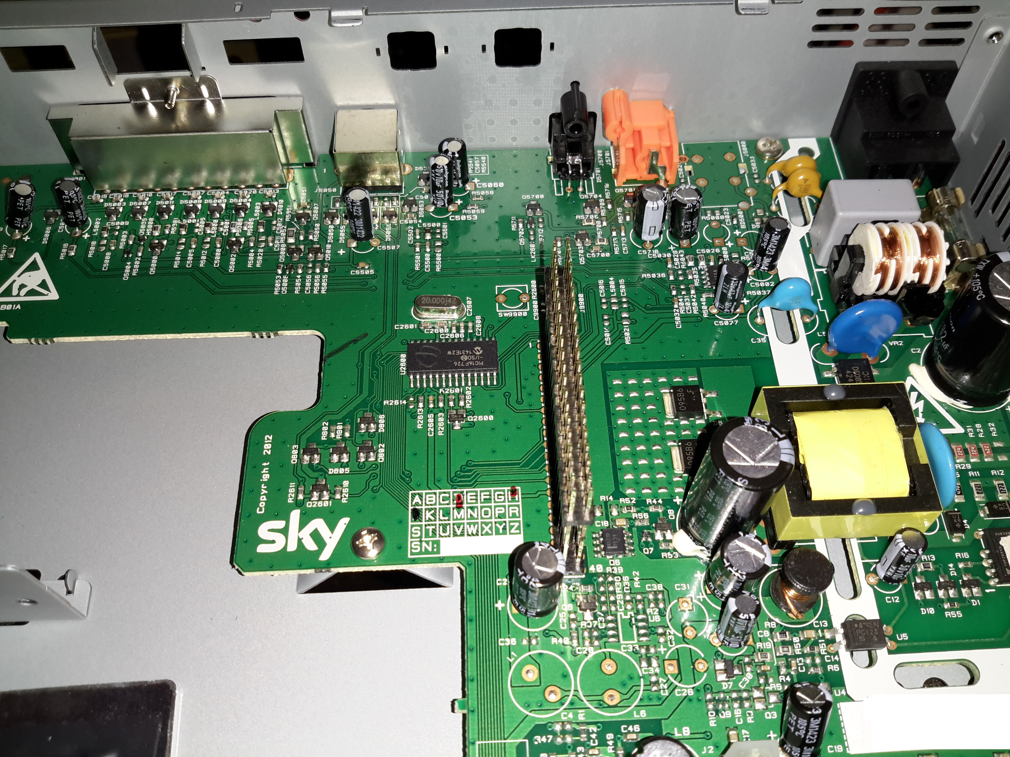
Smart Card Reader
The smart card reader is on the PSU PCB, the controller here is an NXP TDA8024
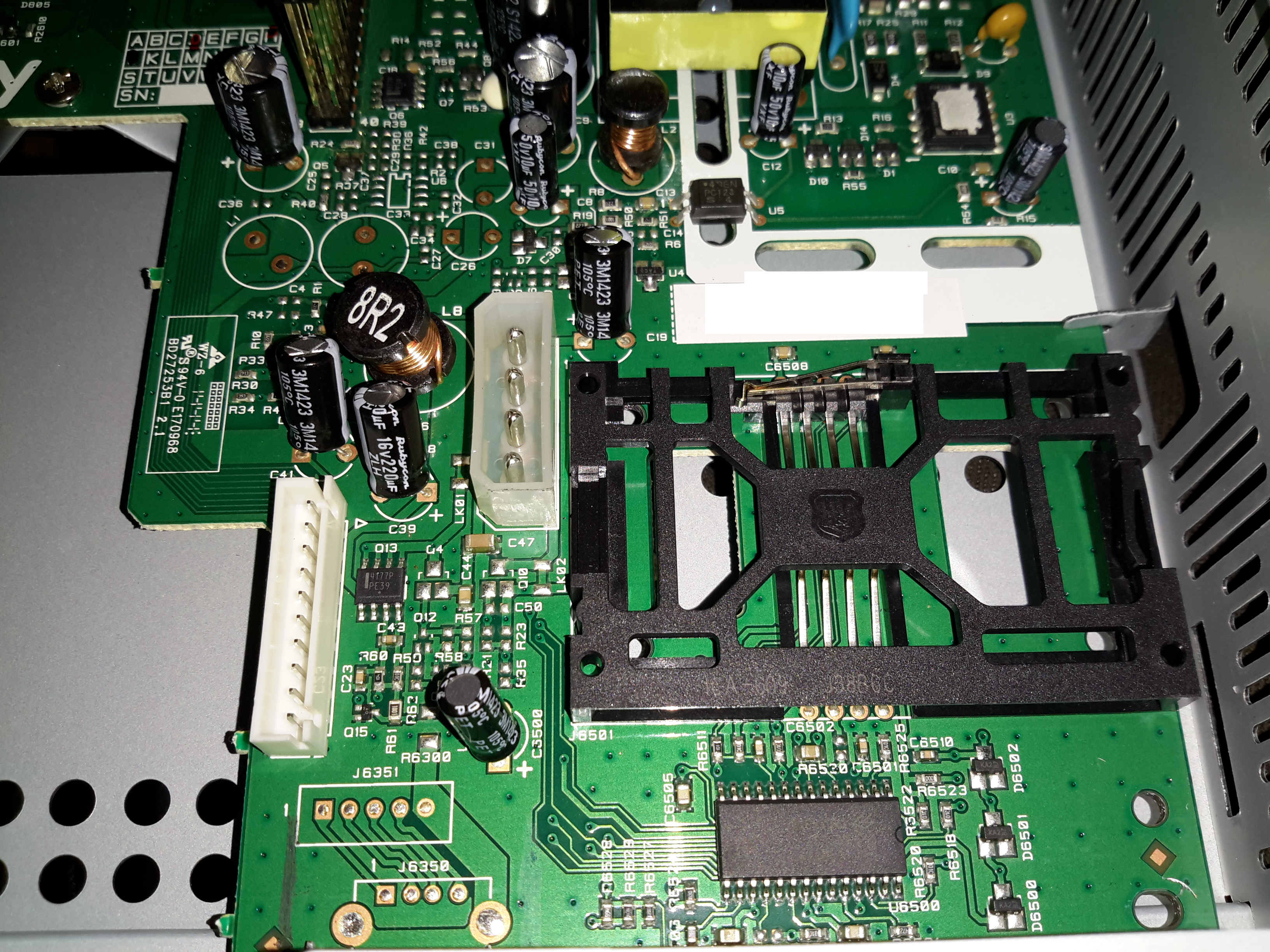
PSU PCB
The PSU itself is a pretty standard SMPS, so I won’t go too far into that particular bit. The logic PCB attaches to the large pin header on the left of the PSU, some of the analogue video outputs are also on this board.
There’s also a Microchip PIC16F726 microcontroller on this PCB, next to the pin header. Judging by the PCB traces, this handles everything on the user control panel.
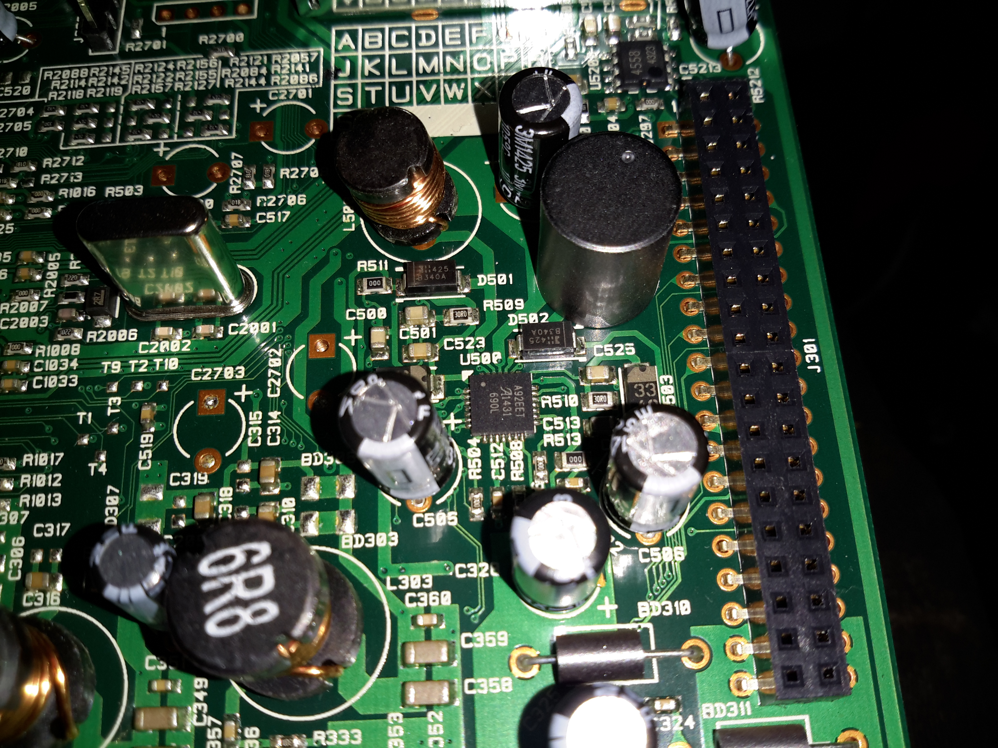
Power Supplies
Some local supplies are provided on the logic board for the main SoC, the IC in the centre here is an Allegro A92 DC-DC converter. I didn’t manage to find a datasheet for this one.
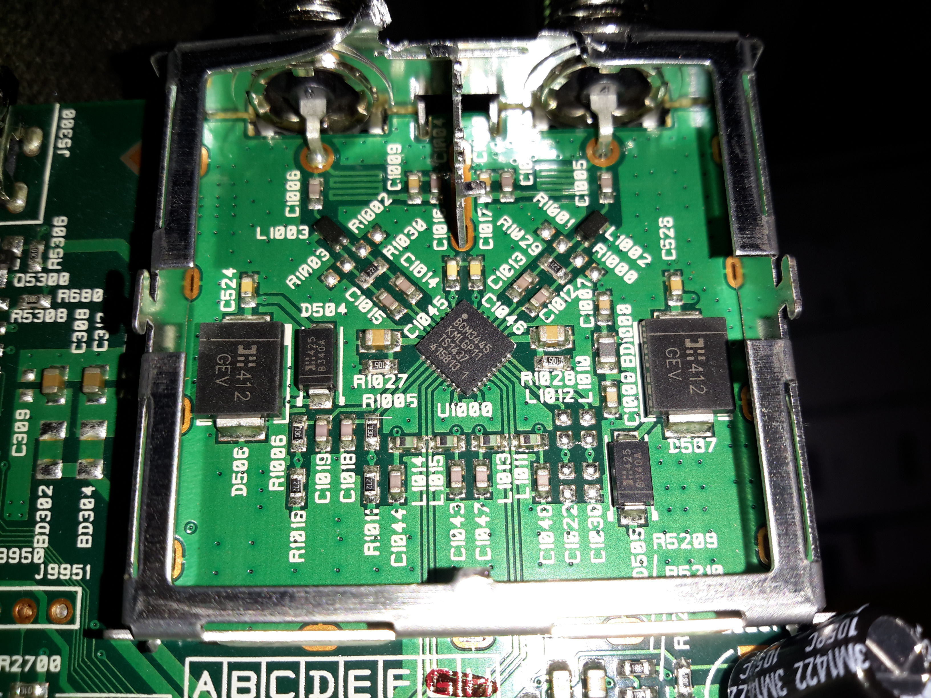
LNB Front End
The RF front end for the satellite input is a Broadcom BCM3445 Low Noise Amplifier & Splitter, again not much info on this one.
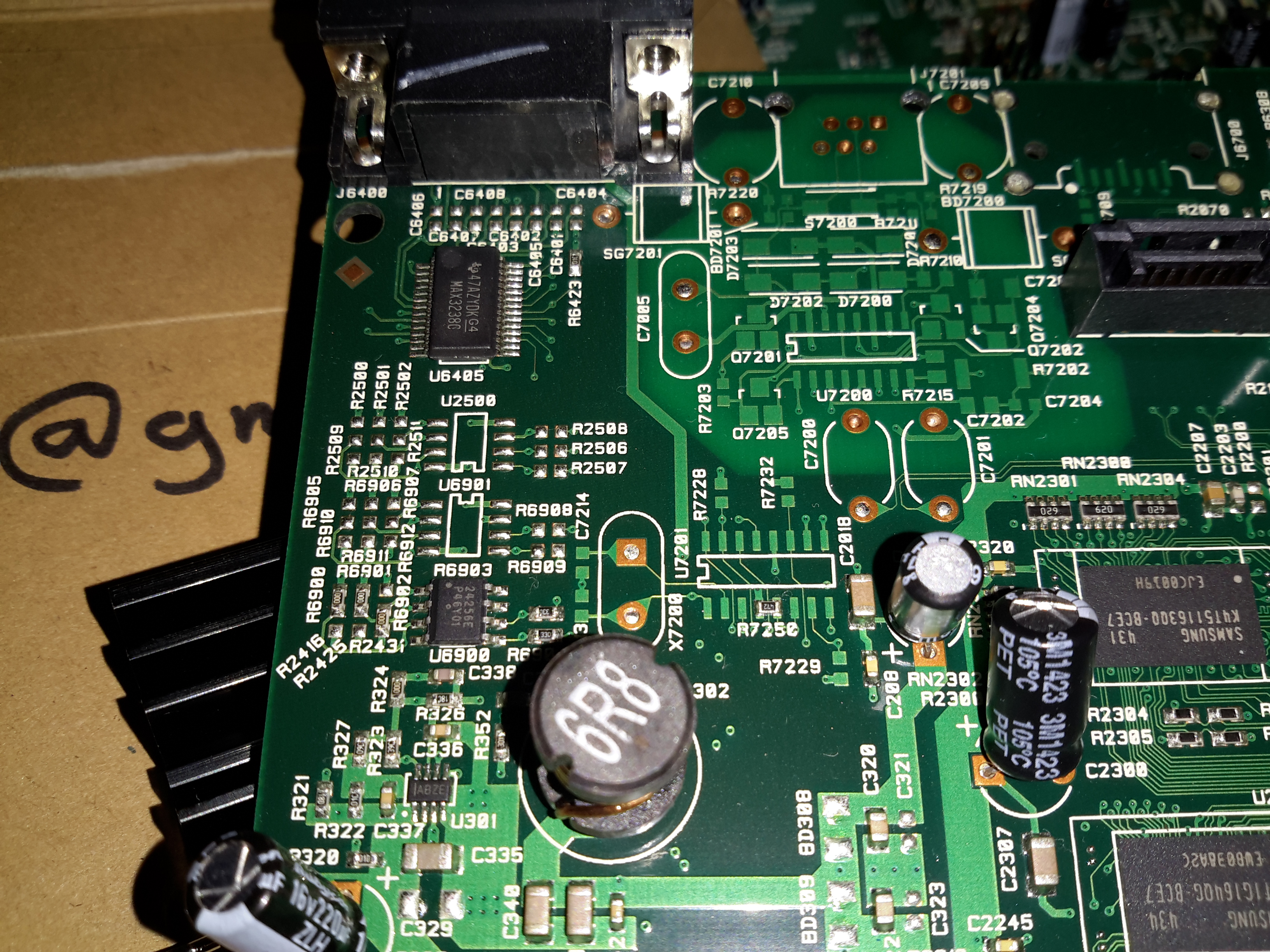
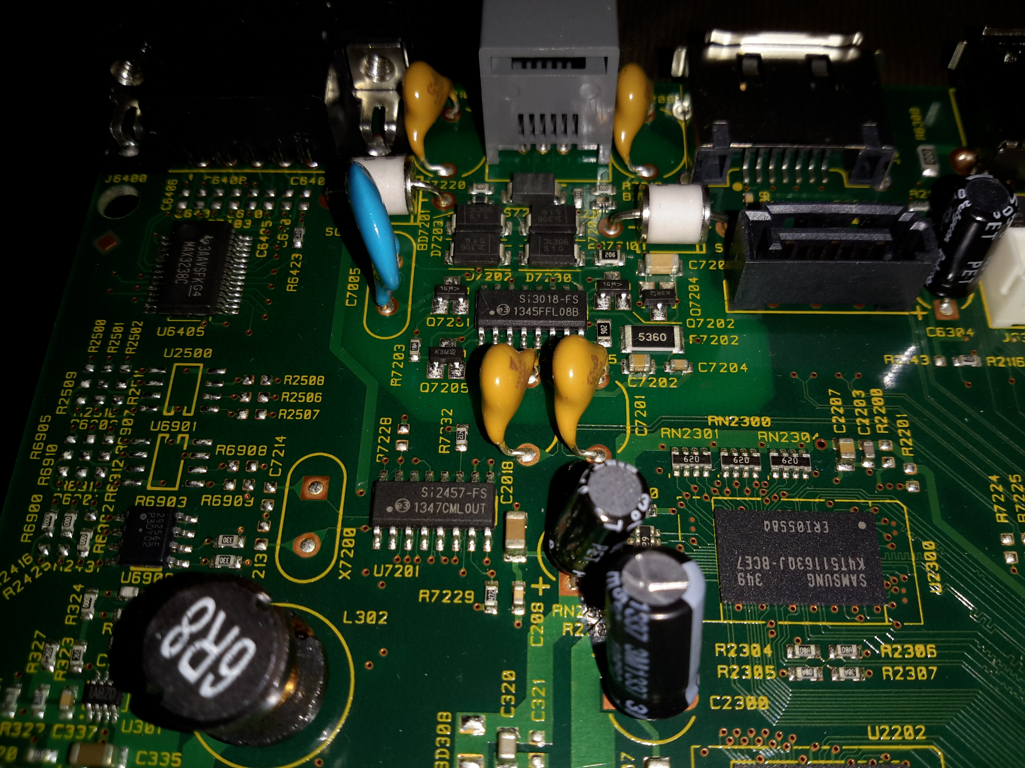
RS232 Section
The standard MAX232 is used for the serial interface. I imagine this is for diagnostics.
Modem
The POTS modem section is handled by a Si2457 System-Side device & Si3018 Line-Side device pair.
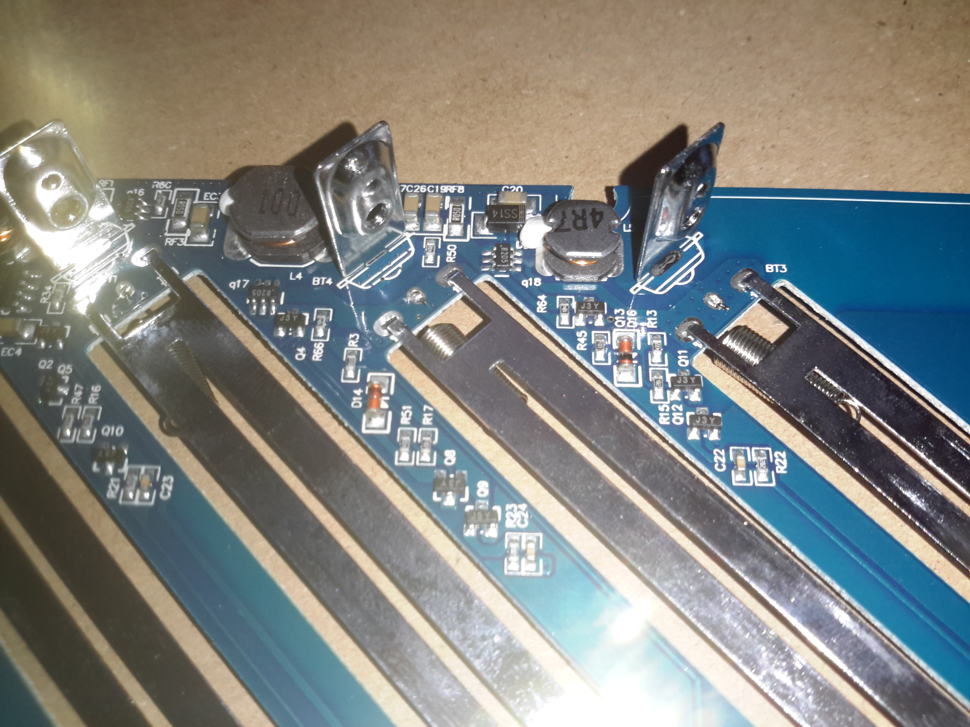
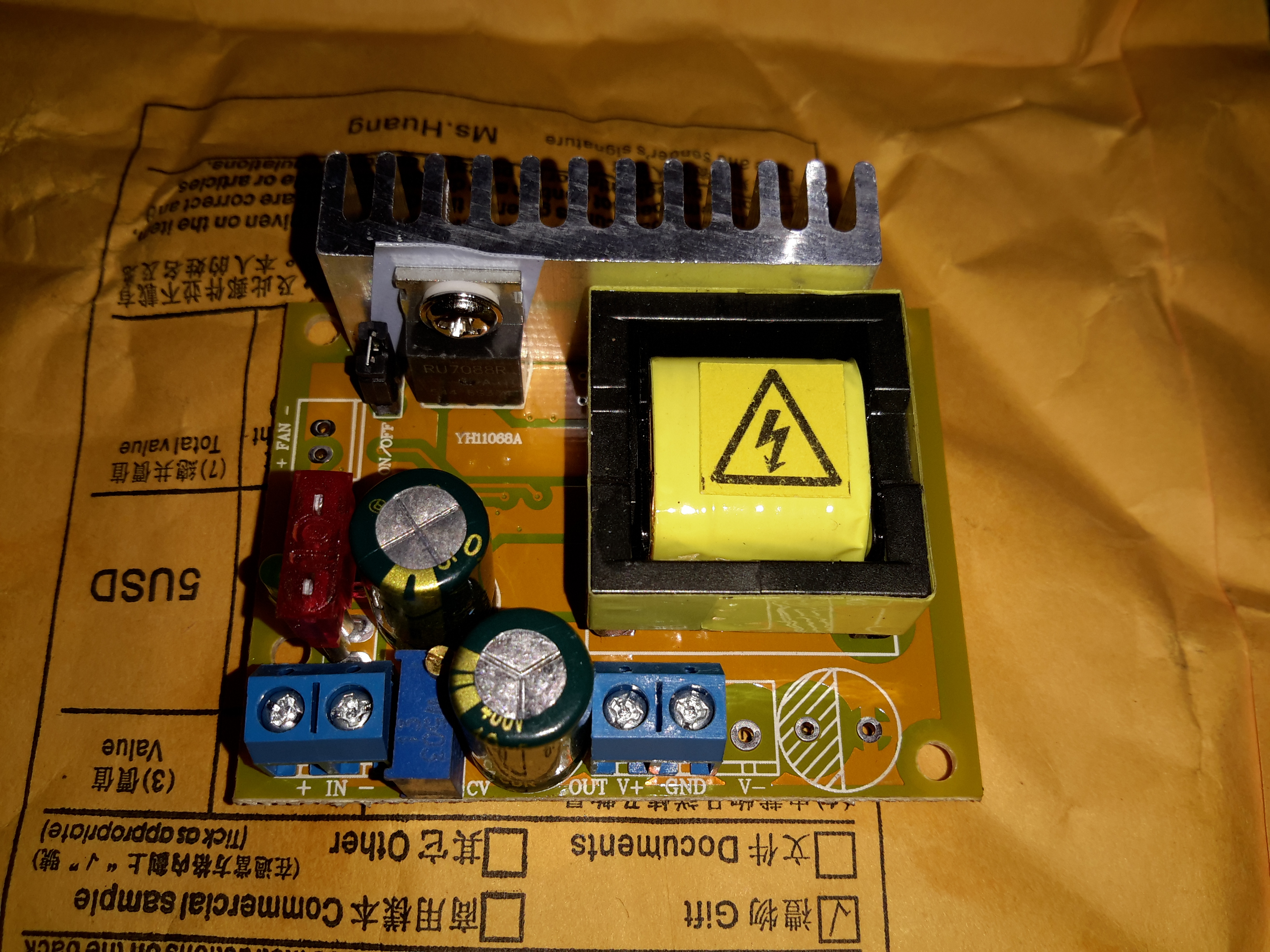
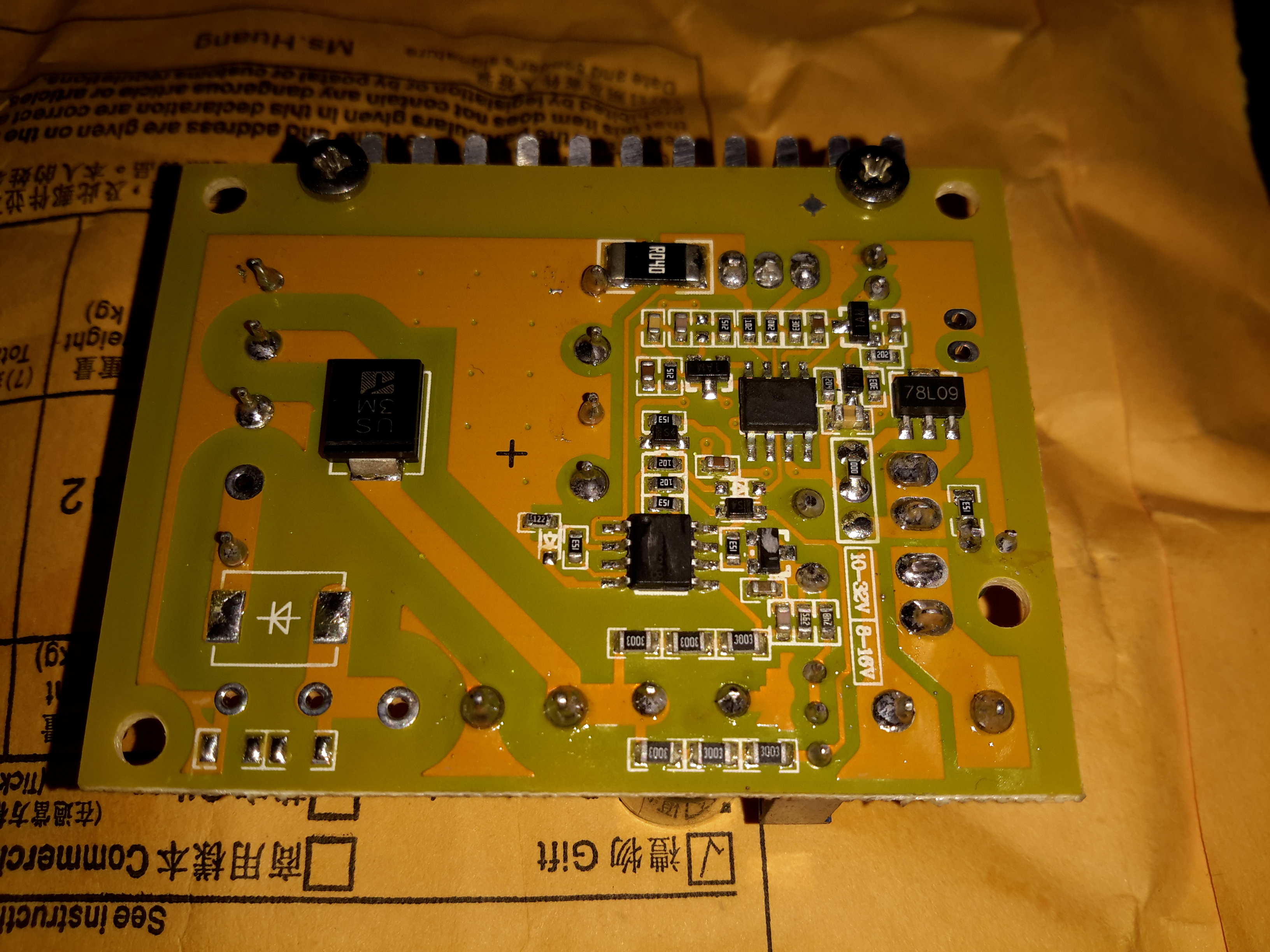
Going through eBay recently looking for parts for a couple of CRT-based projects, I came across these DC-DC converters.
Apparently rated from 45-390v DC output at 200mA, these should be ideal for driving some of the electrodes (focus, screen, grid) in a CRT.
Above is the top of the board, input voltage header on the left, output voltage adjust in the centre & output voltage header on the right.
This module has a mini-automotive fuse, at 10A for input protection.
On the heatsink is mounted the main switching MOSFET, a RU7088R from Ruichips. This FET is fairly heavily rated at 70v 80A, with 6.5mΩ on-resistance.
PCB Bottom
The bottom of the board has the control components, with a pair of ICs. Unfortunately the numbers have been scrubbed off, so no identification here. The output from the transformer is rectified with a single large SMD diode on the left side of the board.
There’s also plenty of isolation gap between the HV output trace & the low voltage logic side of the circuit, the two being bridged only by a resistive divider for output voltage measurement.
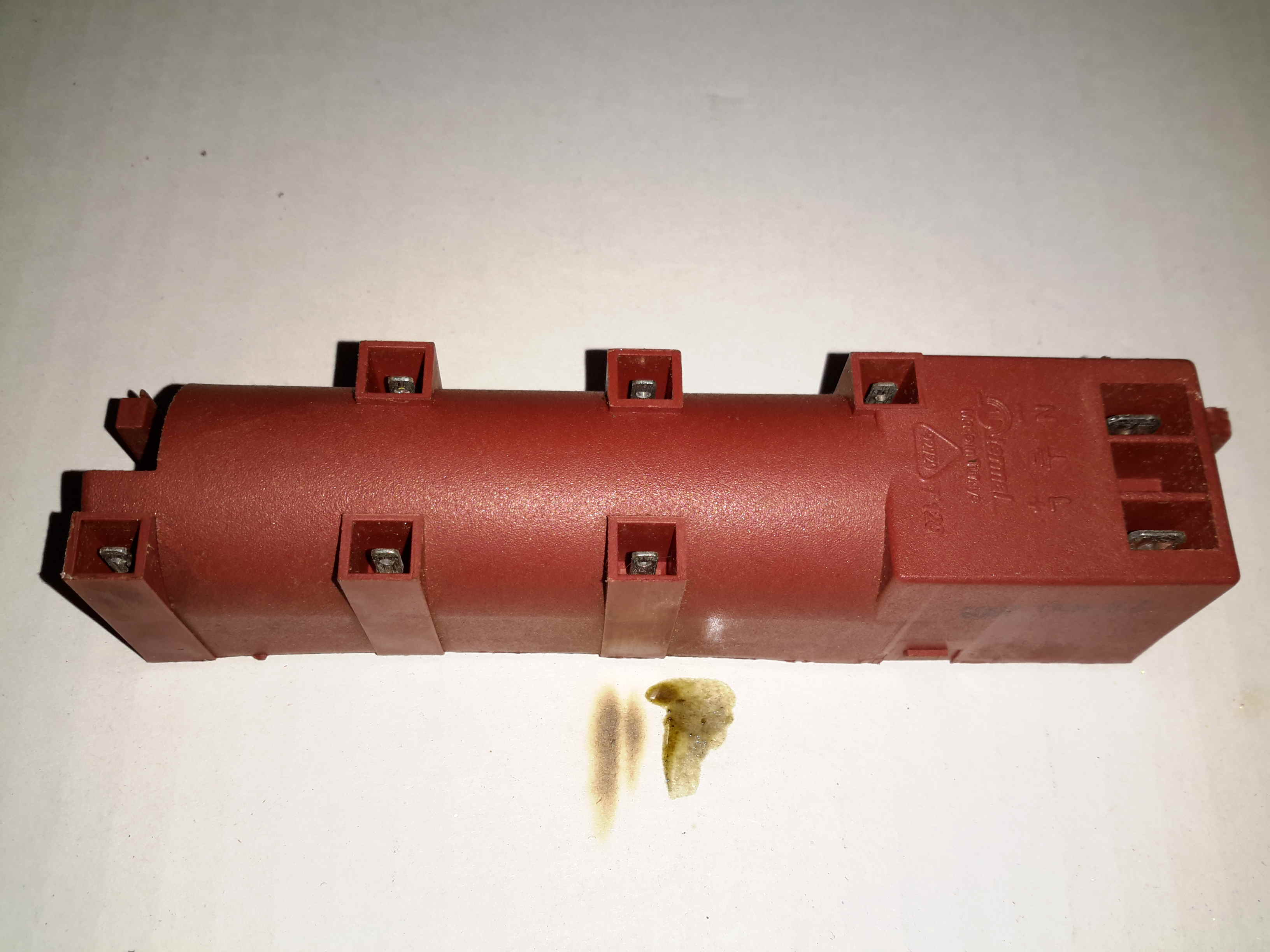
Here’s a quick teardown of an ignition transformer, used on gas fired ovens & hobs. This unit takes mains 240v AC & uses a transformer to step the voltage to several kV, at a low current to ignite the burners.
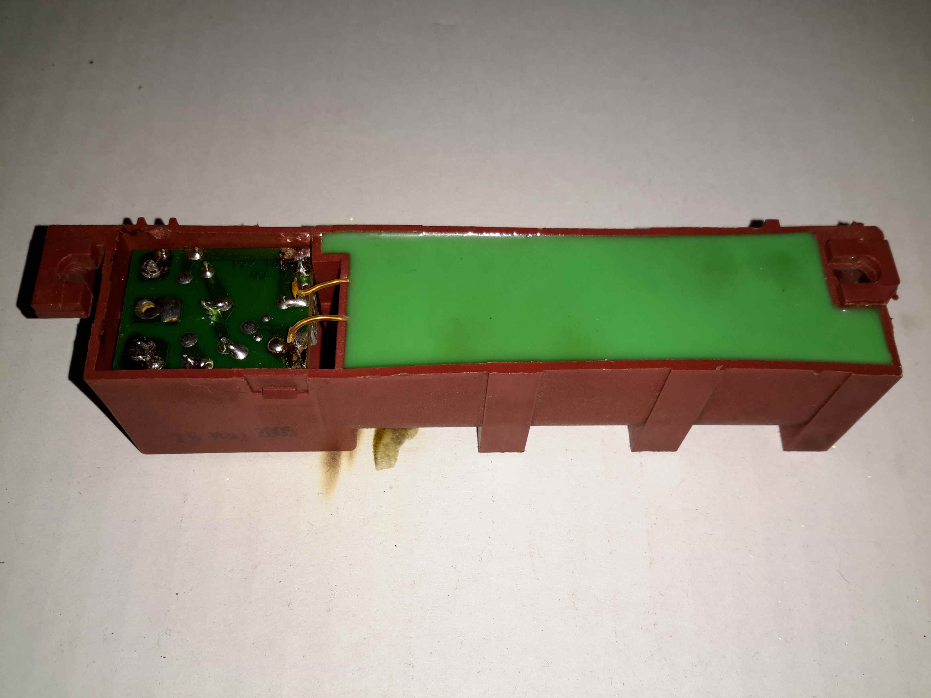
Bottom
The transformer section is completely potted in Epoxy resin for insulation, but the driver circuitry is exposed, with a pair of leads from the primary winding exposed
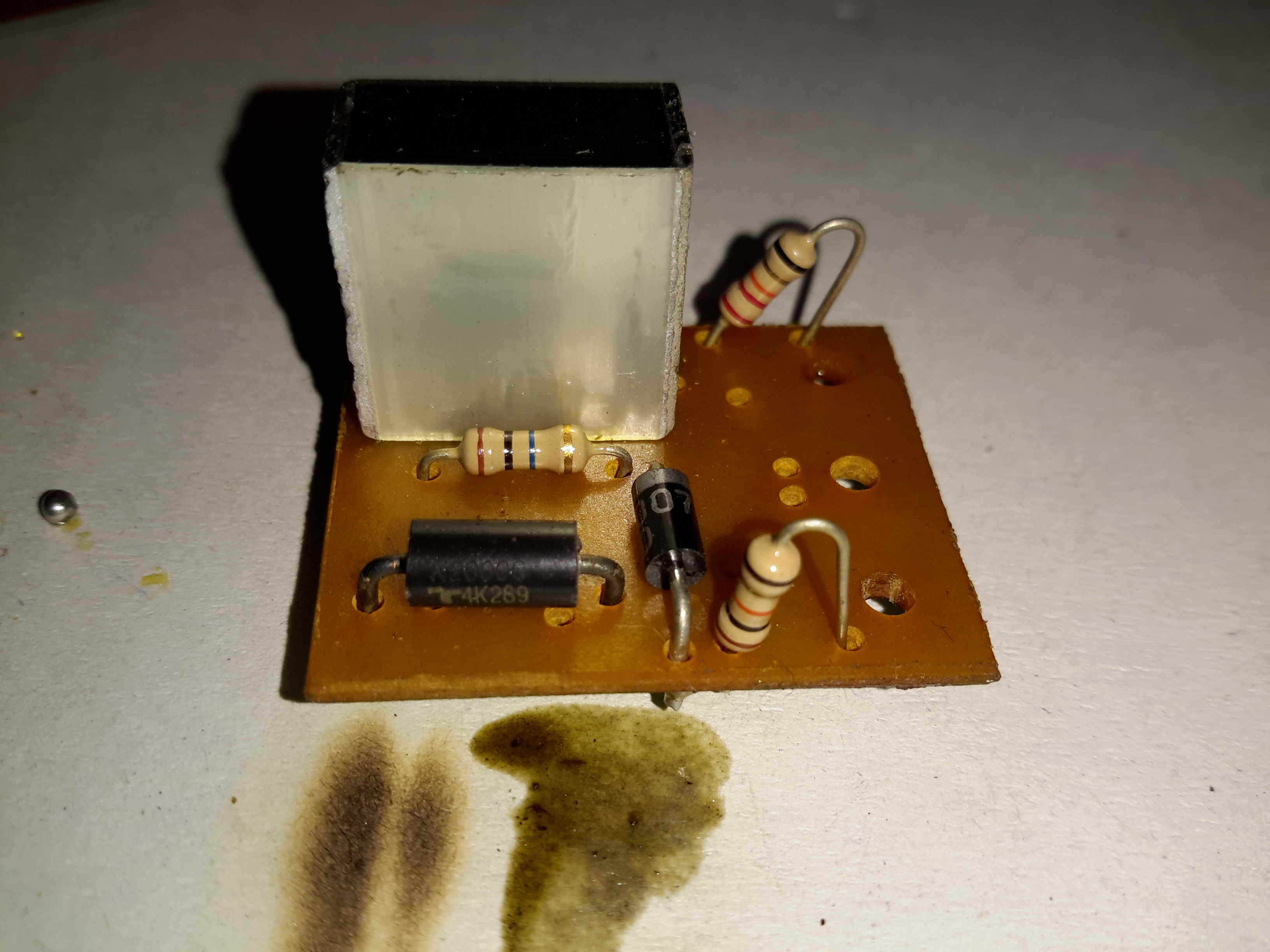
Driver PCB
The drive is very simple. The incoming AC flows through a series resistor through a half-wave rectifier to charge up a 2.2µF film capacitor. Once the voltage on the capacitor reaches a certain level, a DIAC in series with the transformer primary fires, discharging the capacitor through the primary.
The current spike induces a very high voltage on the secondary winding, this then arcs across a gap in the gas flow to start ignition.
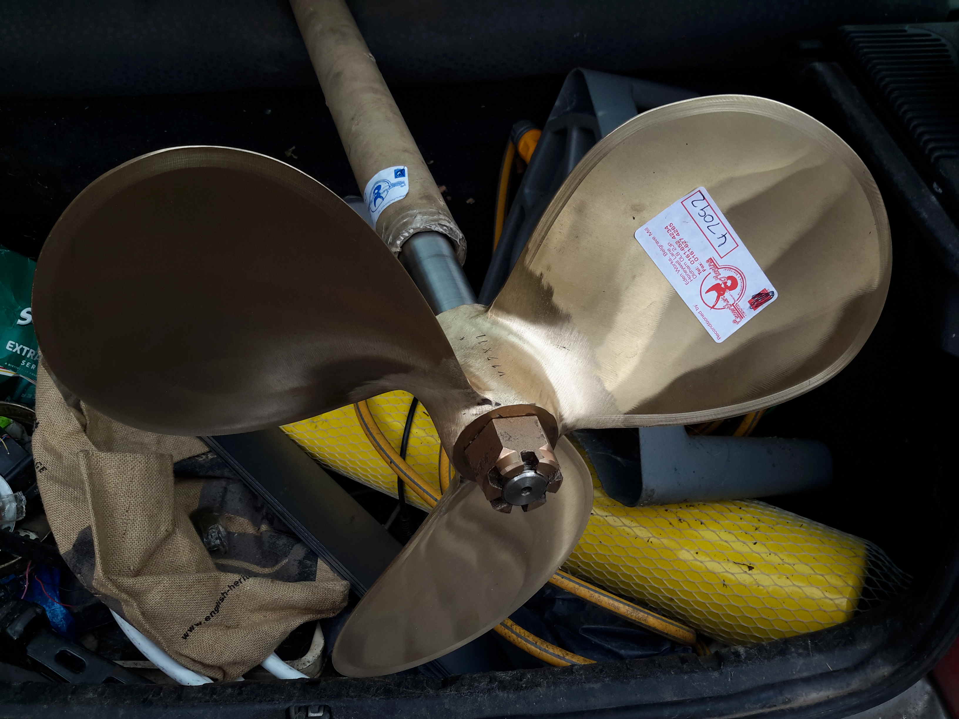
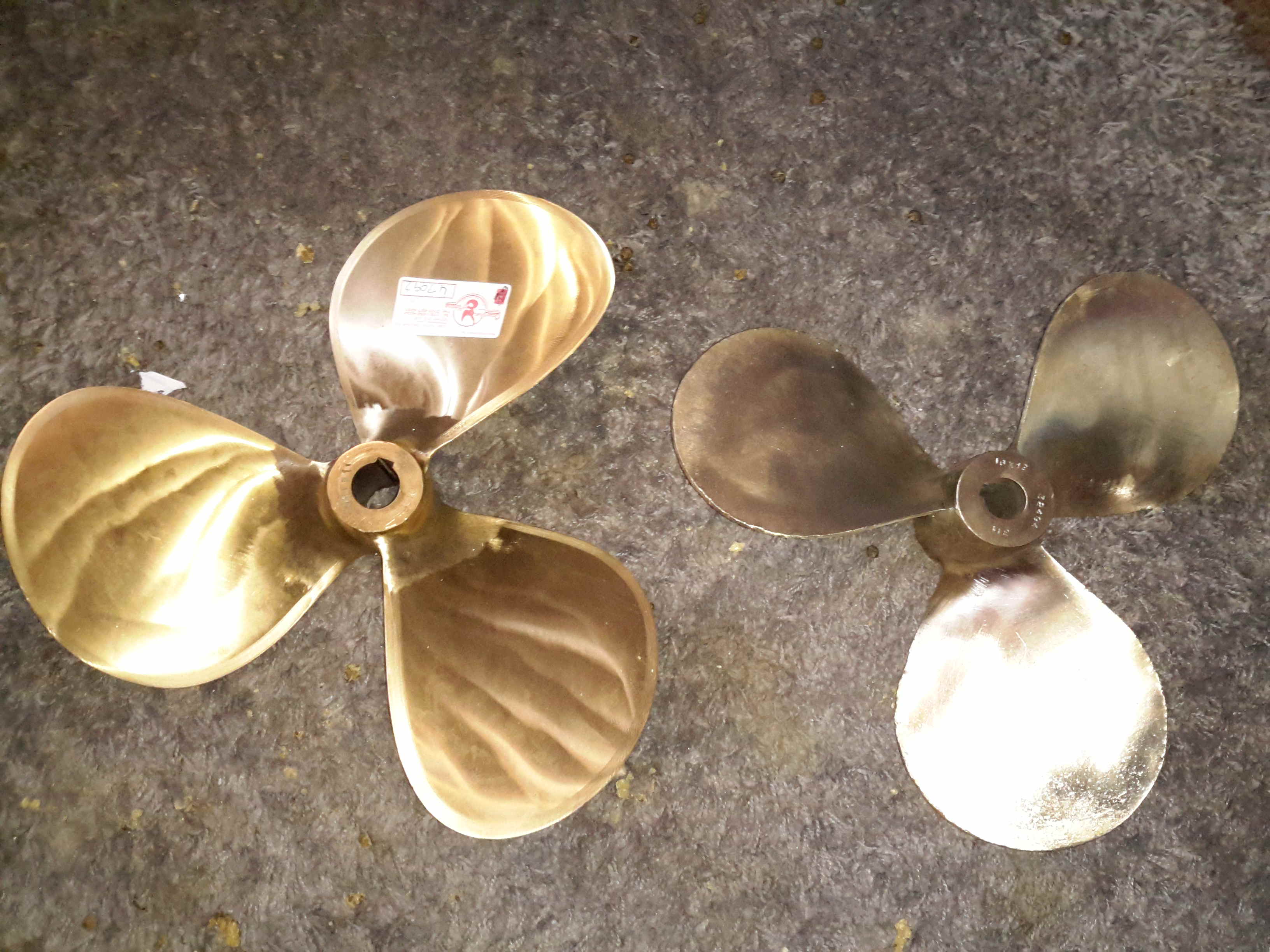
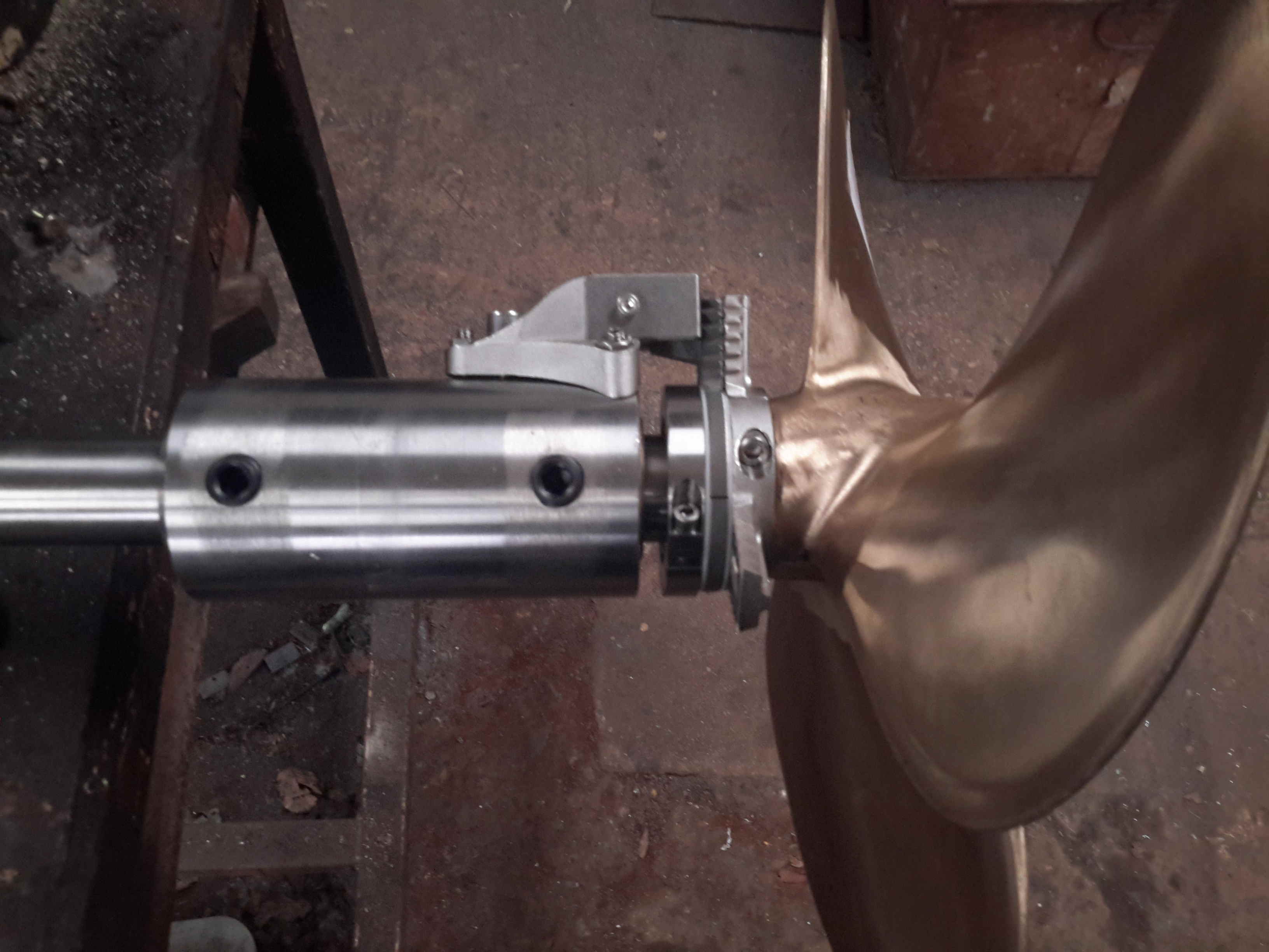
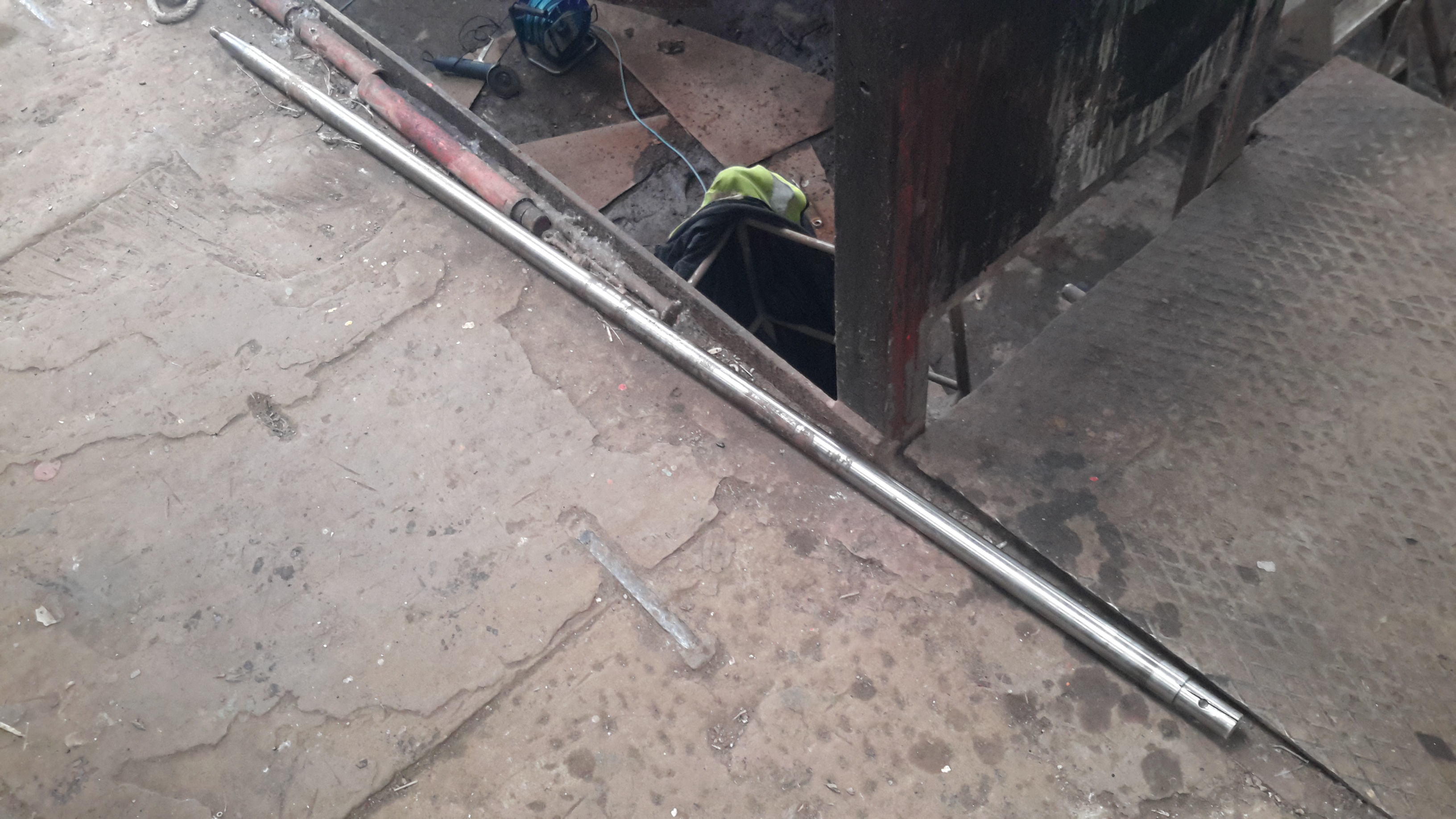
We’re now on the final leg of the jobs to be done on the boat! Above is the new prop & shaft, supplied to us by Crowther Marine over in Royton. To fit our current stern tube & gland, the shaft is the same diamter at 1-3/8″. Unfortunately no 4-blade props were available, so I had to go for a 17×11 left-hand, but with a much larger blade area than the old one.
Propellers
Here’s the old prop on the right, with the new one on the left, amazing how different 1 inch of diameter actually looks. The opposite hand of the new prop makes no difference in our case, as I can simply switch the hoses to the hydraulic motor on the shaft to make everything reverse direction.
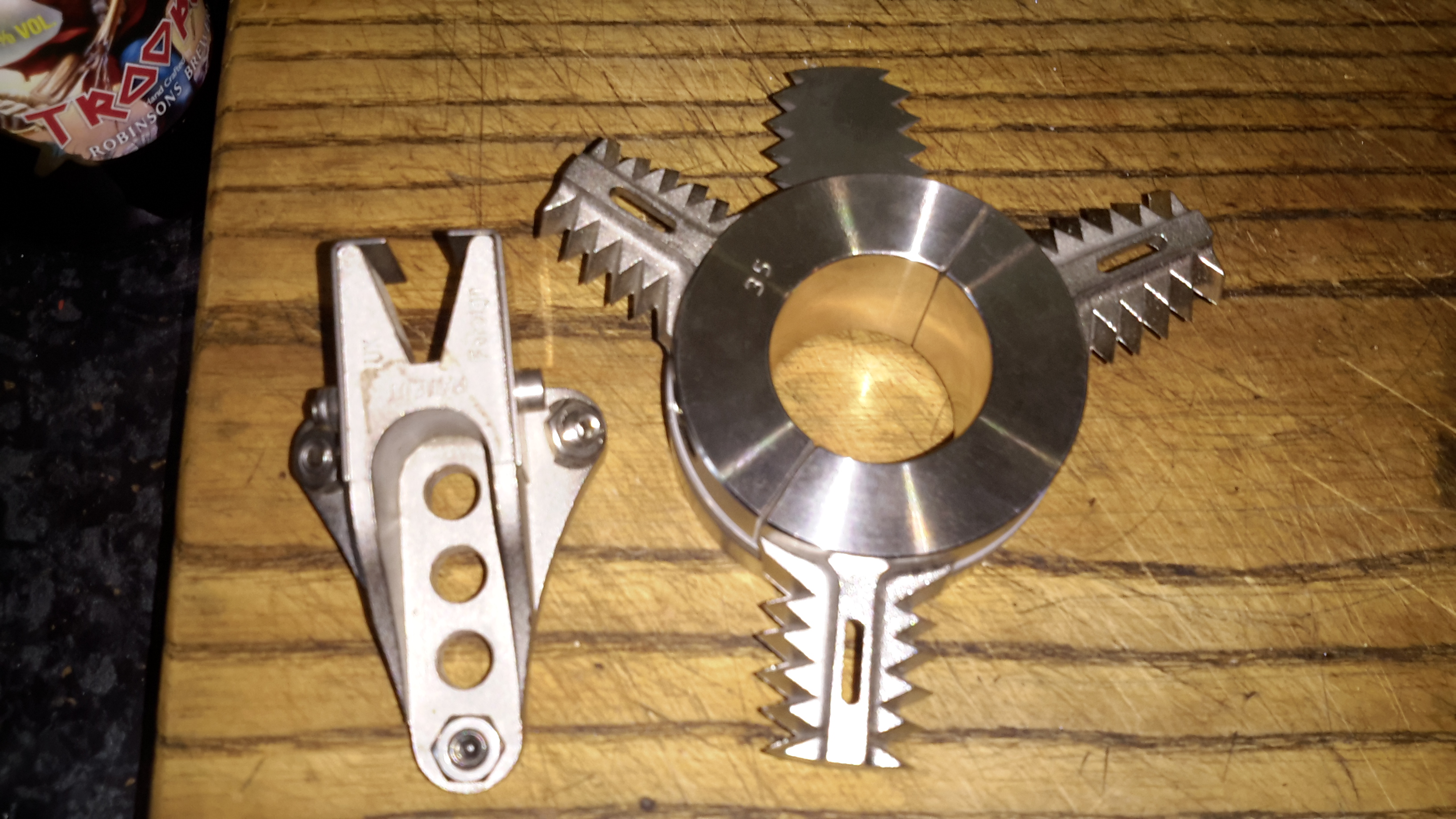
Stripper
Above is the solution to my problem of no weed hatch – a Stripper Rope Cutter from Ambassador Marine. This device has some seriously viciously sharp cutting teeth to help clear any fouling from the prop in operation. Only time will tell if it’s effective at allowing me to stay out of the canal manually removing the crap!
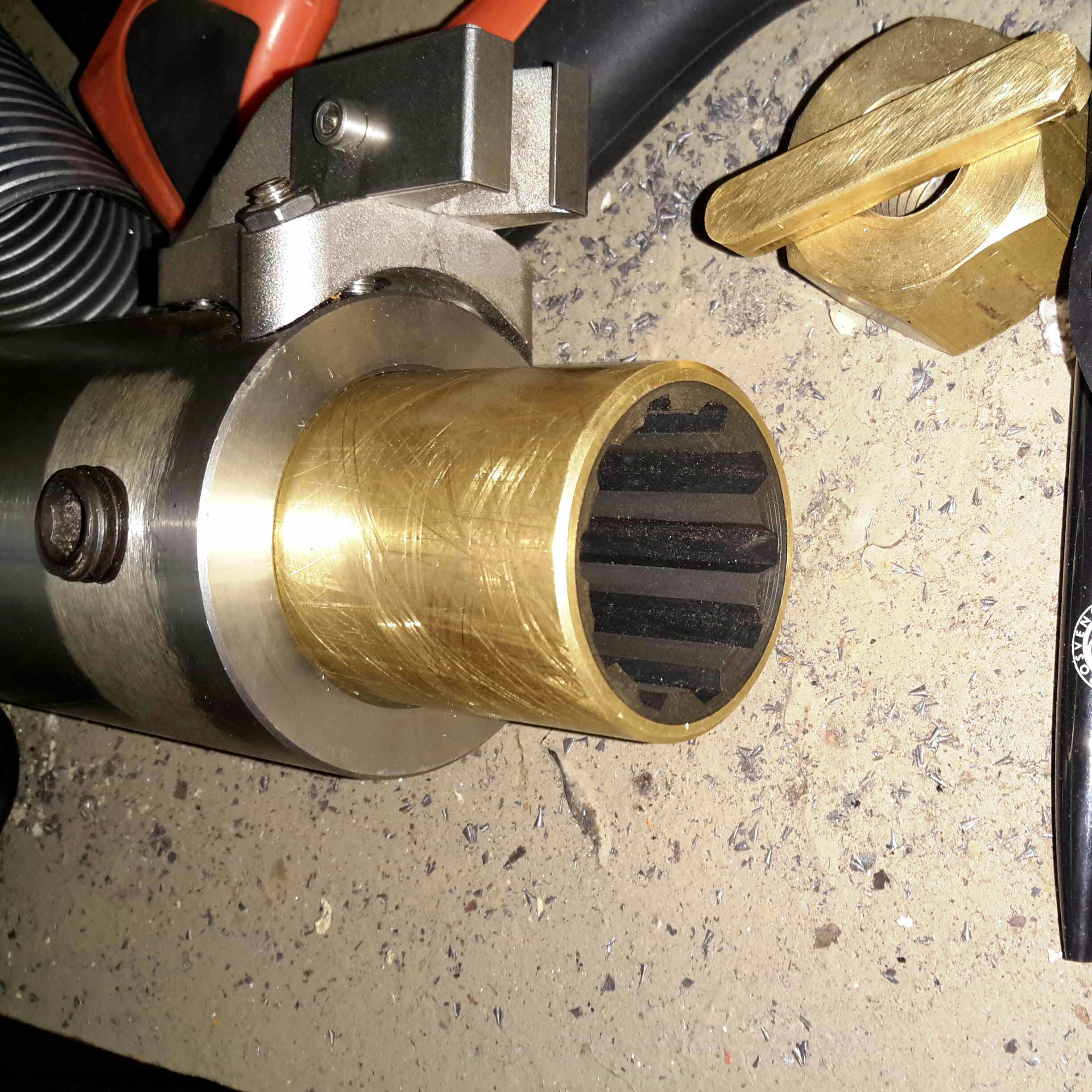
Cutless Bearing
We finally got the bearing mount finished, by S Brown Engineering in Stockport. This is made from Stainless steel to stop the bearing corroding in place & becoming a real arse to replace. Set screws are fitted to make sure the bearing doesn’t move in service.
Attached to the side of the bearing housing is the fixed blade mounting for the Stripper Rope Cutter.
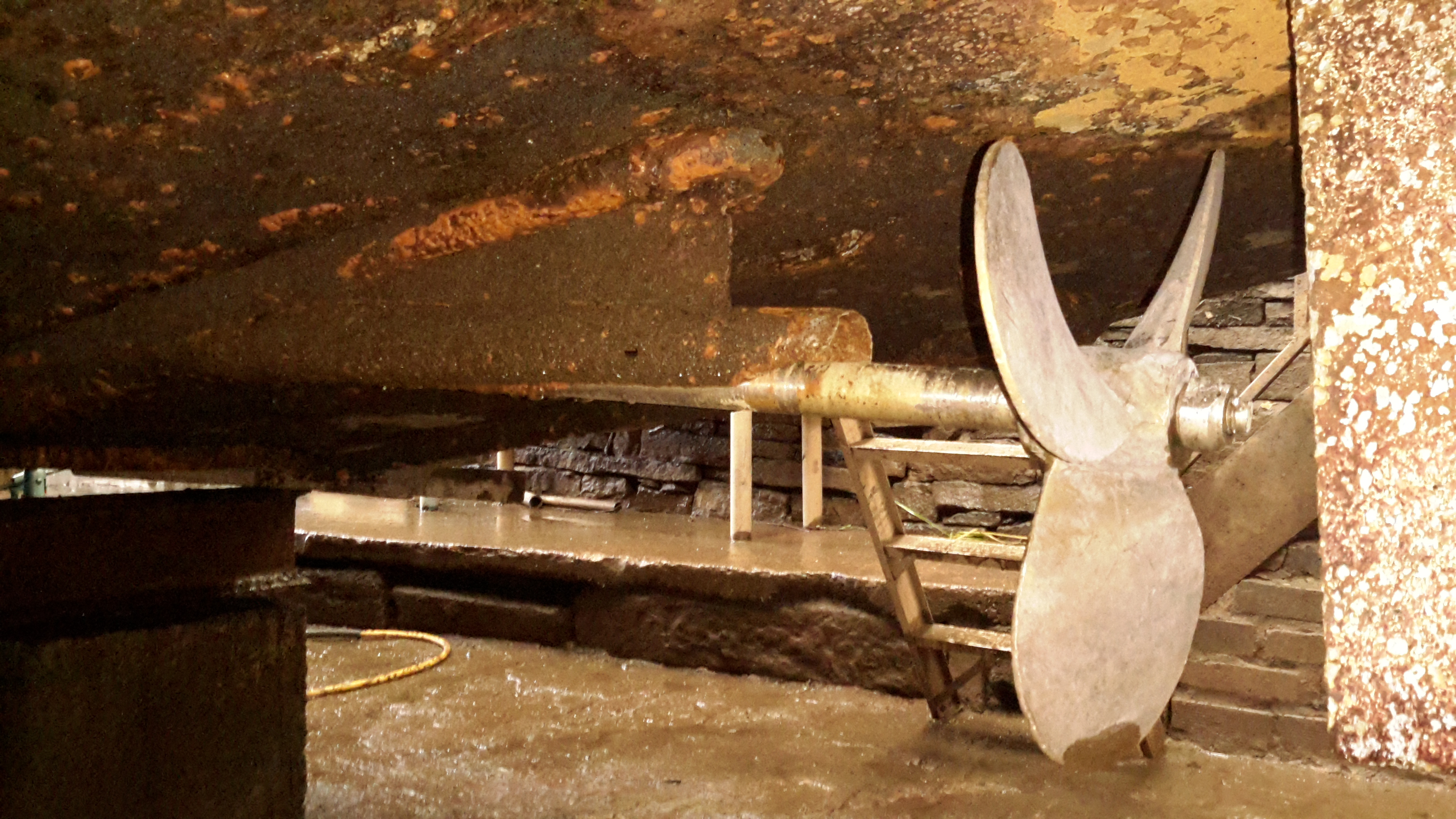
Bearing Test Fit
Above is everything fitted to the shaft for a test before the gear went into it’s home in the stern tube. The Stripper mounts behind the prop, clamped to the shaft. The 3 moving blades move against the fixed blade like a mechanised pair of scissors.
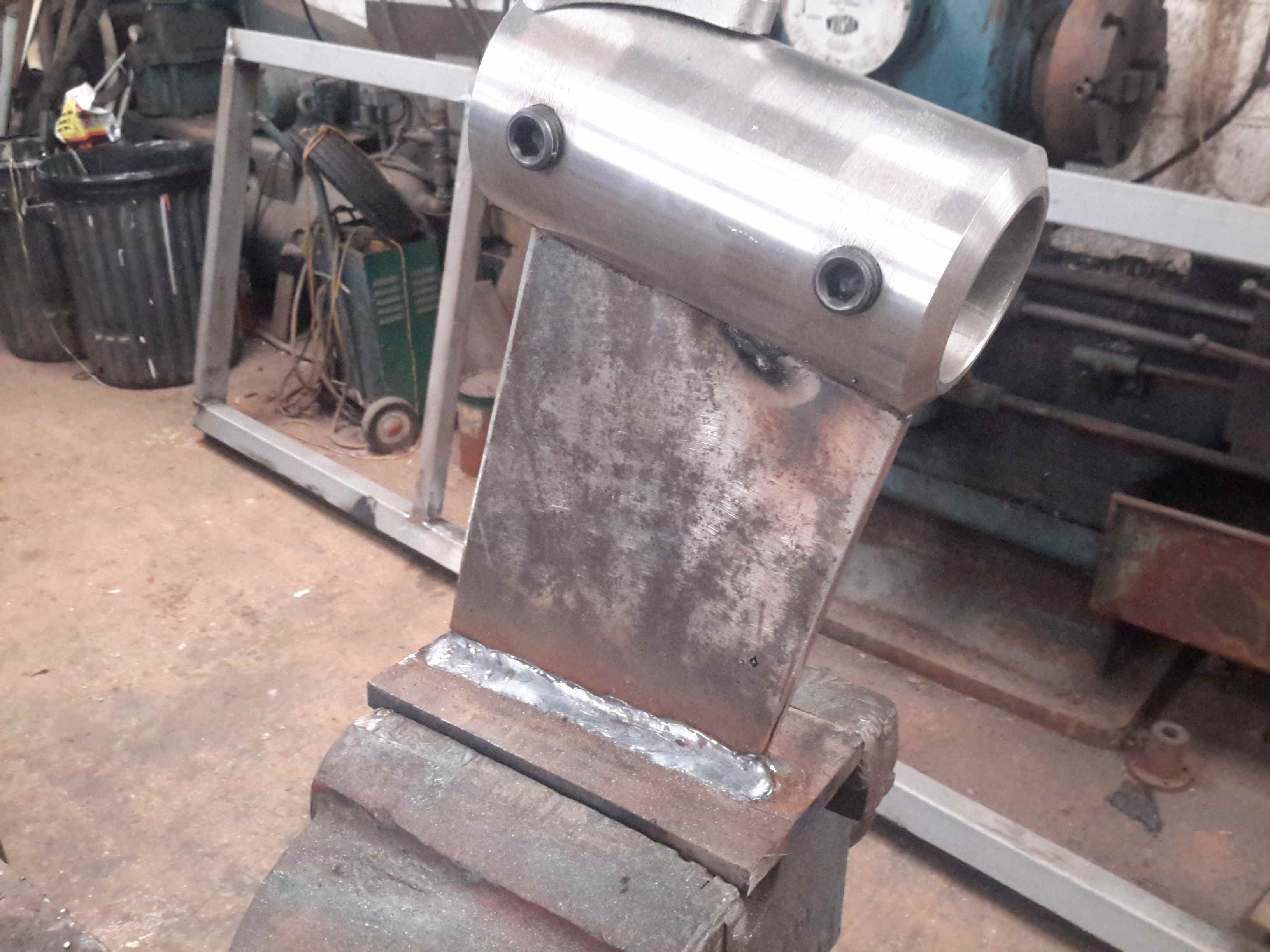
Bearing Strut Welding
10mm steel plate has been used to make the strut for the bearing tube, welded together. In the case of the joint between the stainless tube & the carbon steel strut, special welding rods were needed, at the price of £2 a rod! Using mild steel rods to weld stainless could result in cracking of the welds. Not a good thing on a prop shaft support bearing.
Sand Blasted Hull
Most of the old tube has been cut away to make room for the new bearings, and the bottom of the hull has been sand-blasted ready for welding.
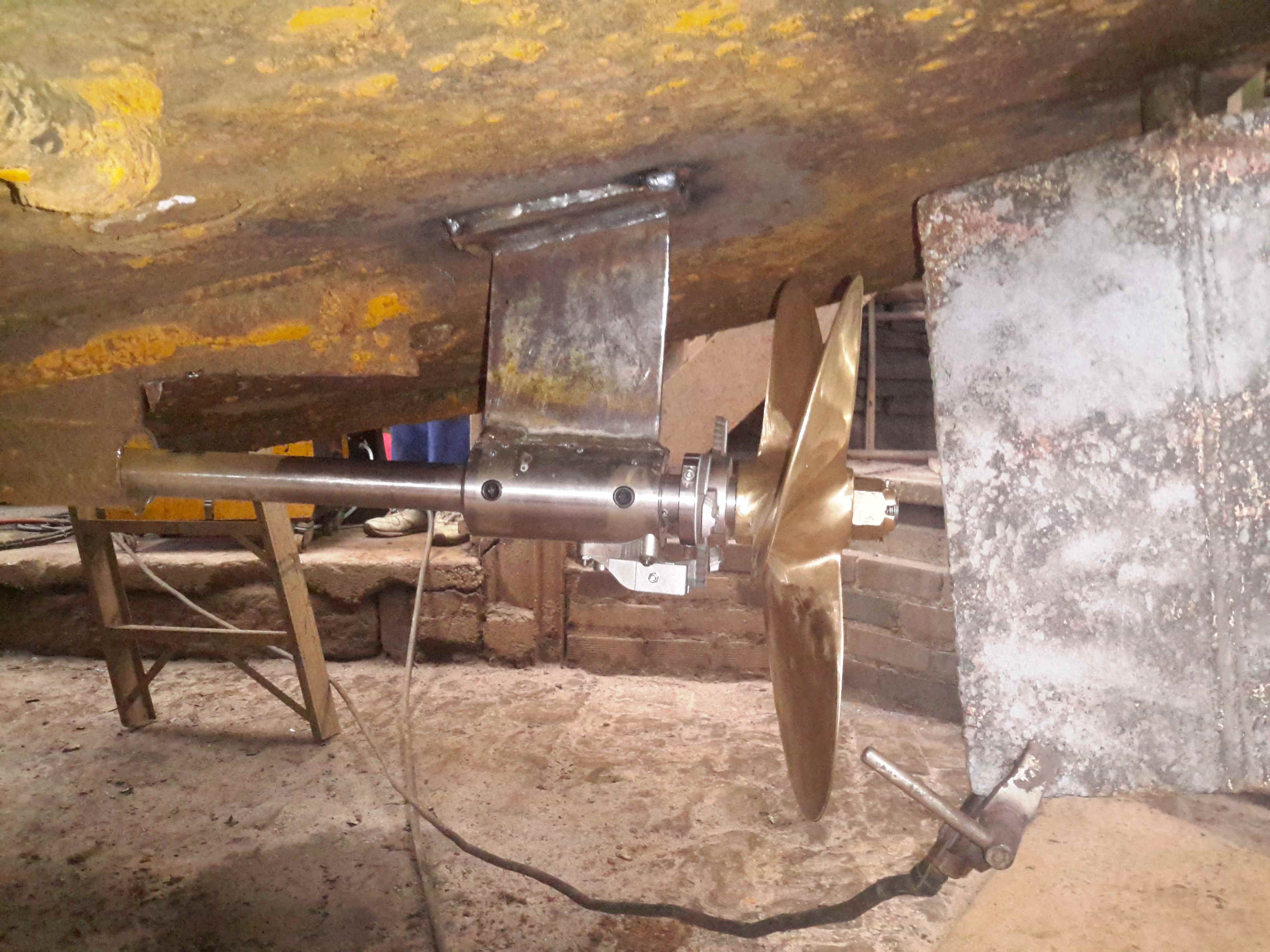
Running Gear Mounted
The bearing mount is welded to the hull, the Stripper & the prop are fitted to the end of the shaft. There’s 1.5″ of clearance from the blade tips to the hull plating. The rudder has about an inch of clearance to the end of the shaft.
Rudder Fence
To help keep the prop wash down, directing more of the force into moving the vessel rather than creating a nice rooster tail, a pair of plates has been welded onto the rudder. These also provide a handy step should someone fall in ;).
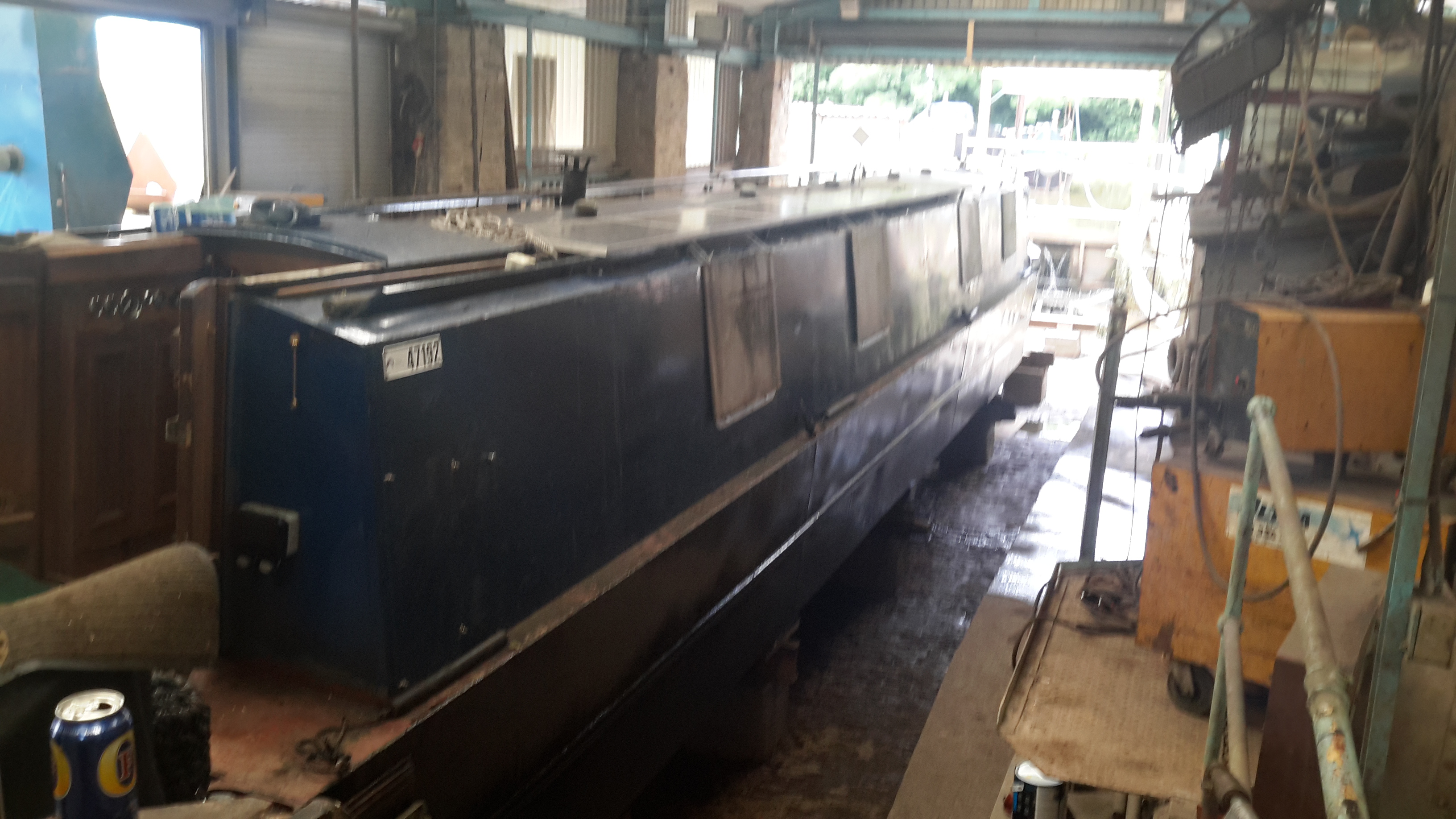
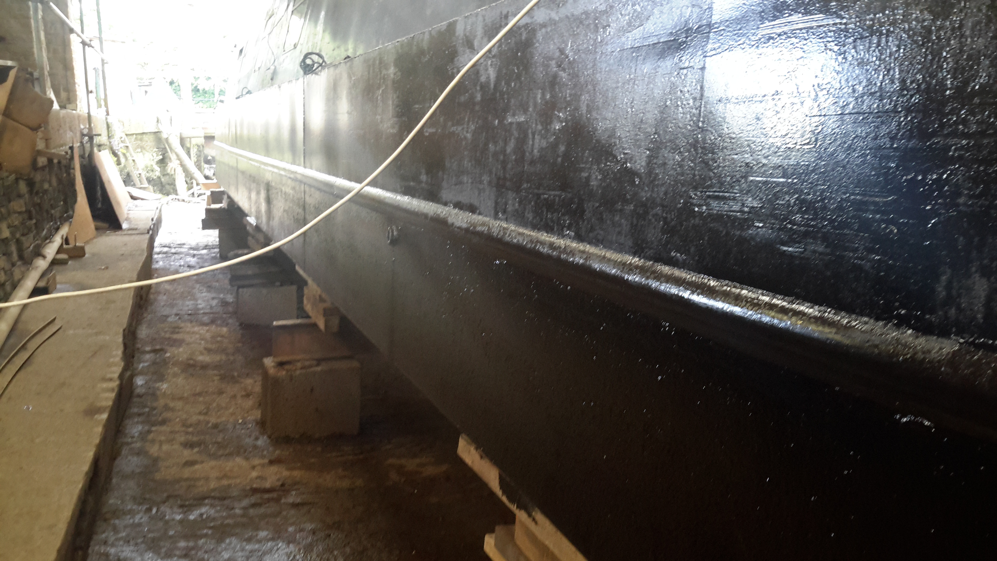
Things are coming along nicely with this year’s drydock operations.
Blacking – Second Coat
Shes looking much better, the second coat of bitumen blacking is on, we’re going to continue at a coat a day until we’re due back in the water.
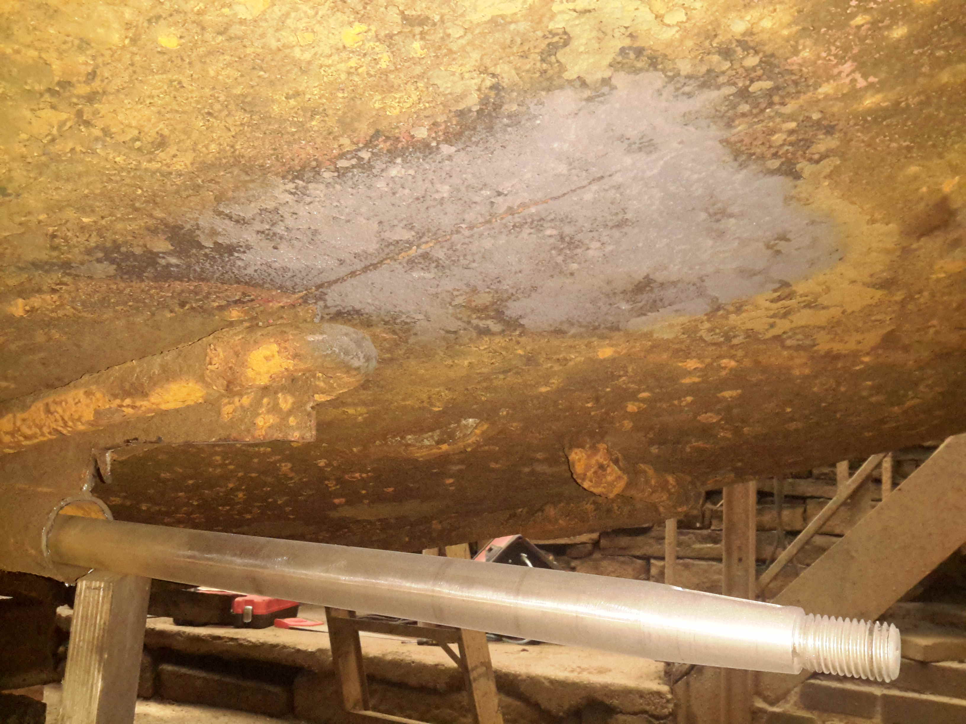
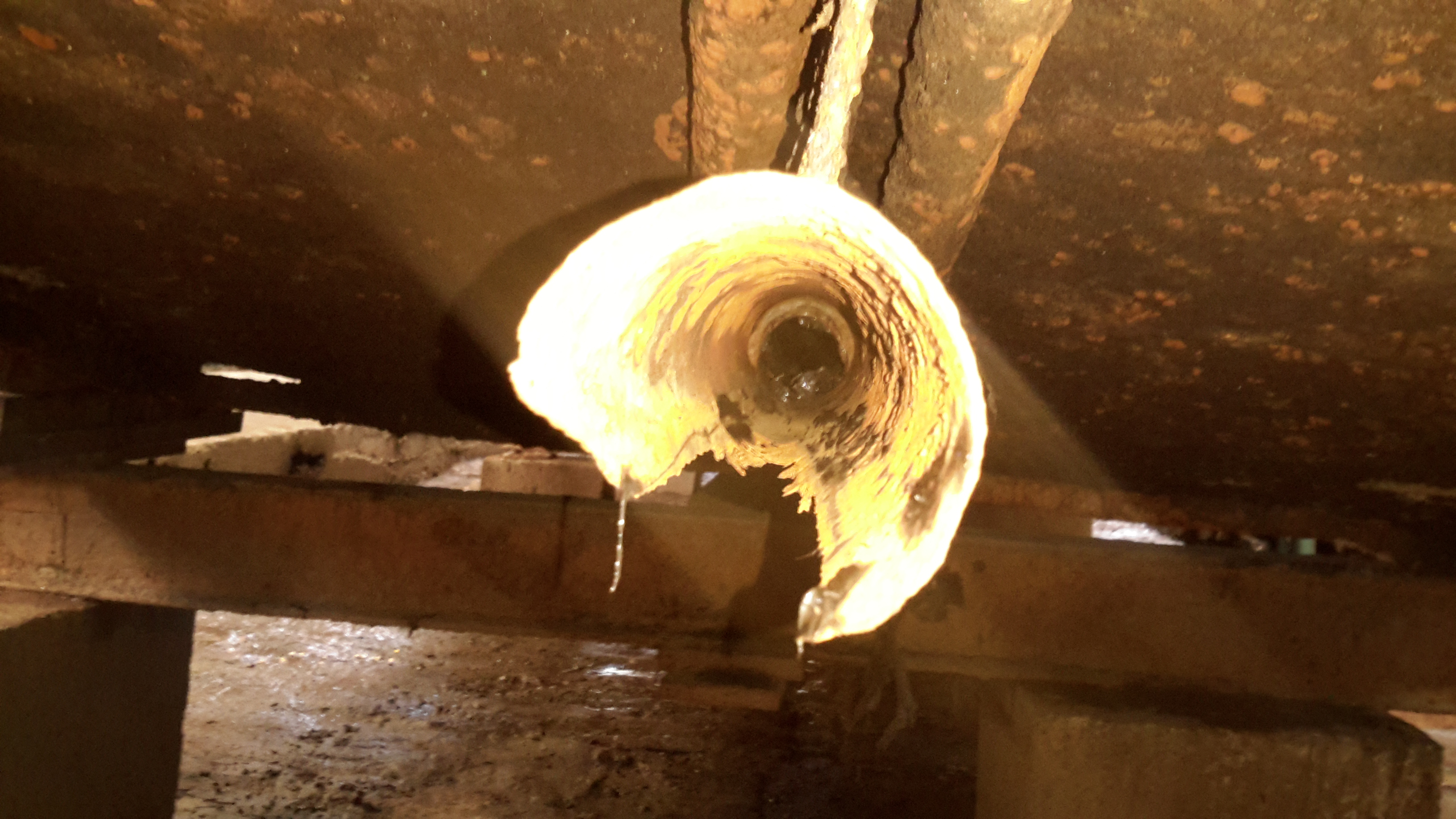
Shaft Tube Damage
I’ve now removed the shaft from the stern tube to gain better access, now the full extent of the damage to the tube can be seen. There’s nothing left at all of the old bearing, which on this boat was simply a nylon bushing pressed into the end of the tube. (I knew it was crap the last time we were out, but ran out of time to get a fix done).
The stainless shaft, having lost it’s support bearing at some point, has been running on the inside of the steel tube, and has neatly chewed straight through it.
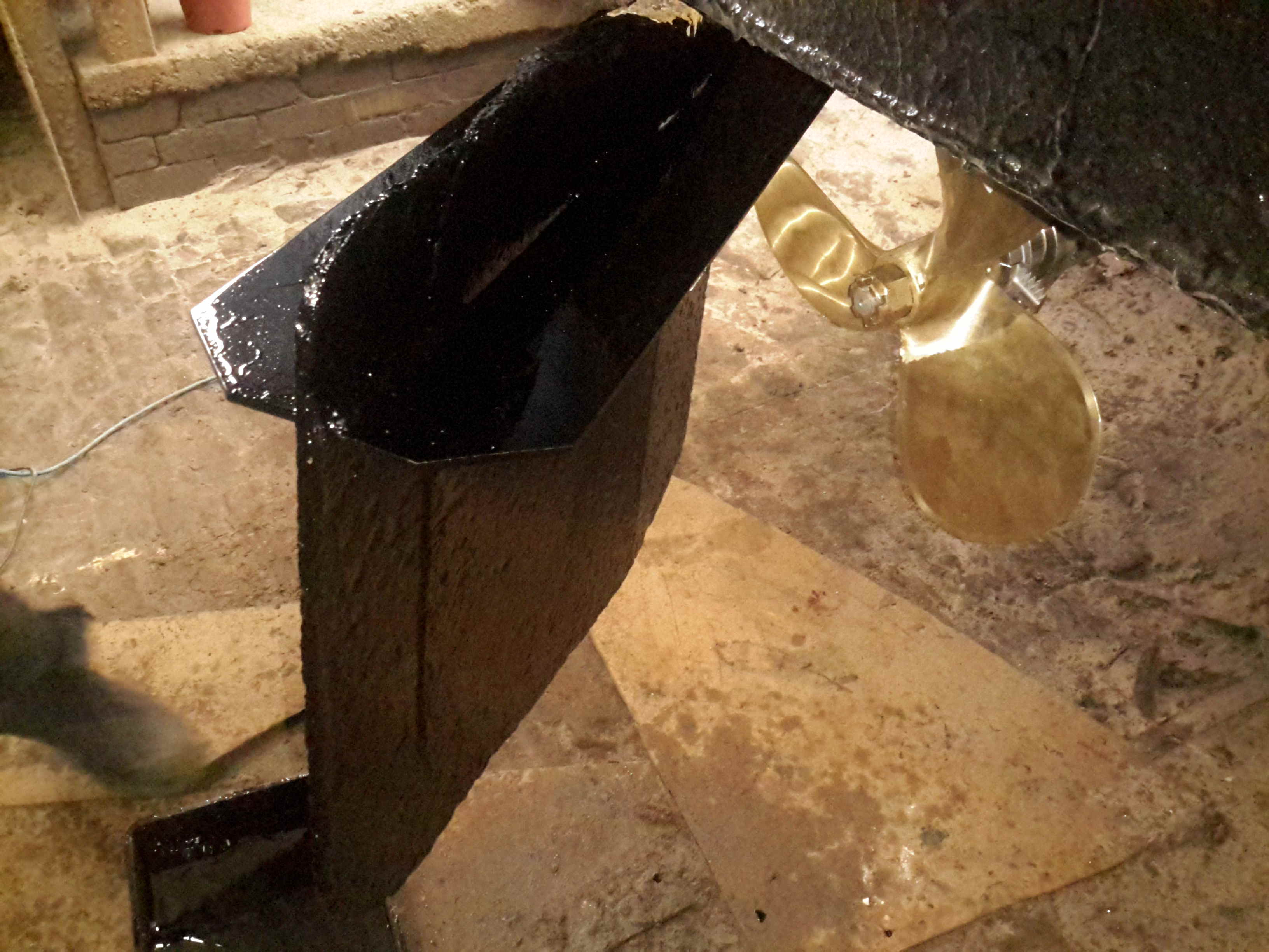
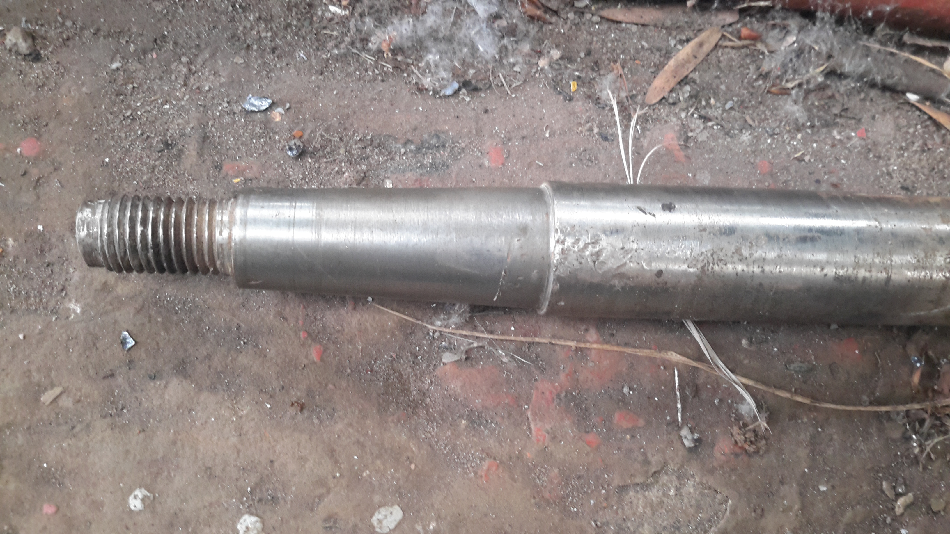
Prop Shaft
Here’s the prop shaft removed from the boat – possibly the longest shaft I’ve ever seen on a narrowboat at 6′ 2″. Unfortunately, the fact that it lost the bearing has also damaged the shaft itself, this will have to be replaced.
Prop Taper
Here’s the end of the shaft that would run in the end bearing, it’s badly scored & fitting a new bearing to this shaft would cause failure very quickly. The taper on the end isn’t much better, and a loose fit in the prop has done some damage there also.
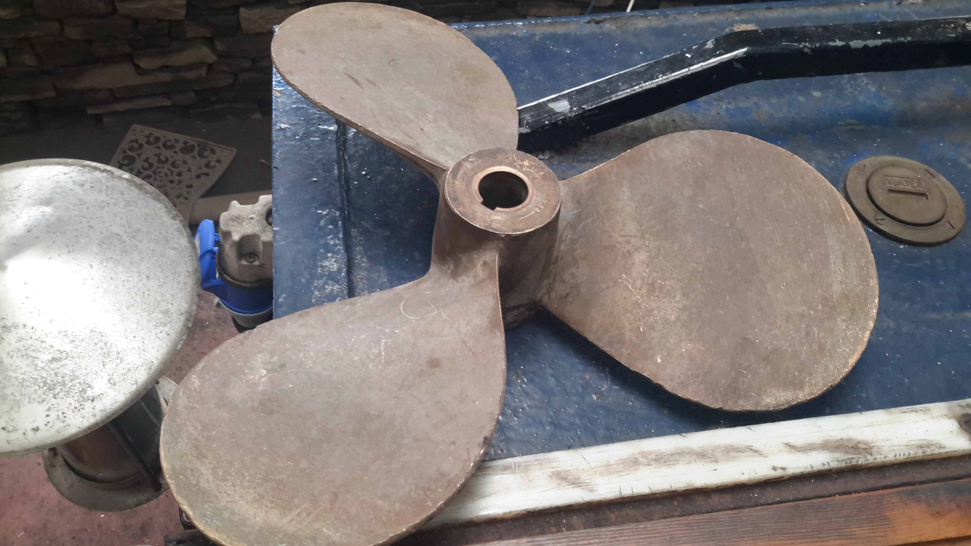
Old Prop
Here’s the old prop – a 16×12 that was only fitted a few years ago. This will be replaced with a new 4-blade prop, as this one is far too small for the size of the boat & installed power. Installing a larger diameter prop isn’t possible due to clearance from the swim, so I’ll have to get a more steeply pitched prop, with 4-blades for increased contact area with the water.
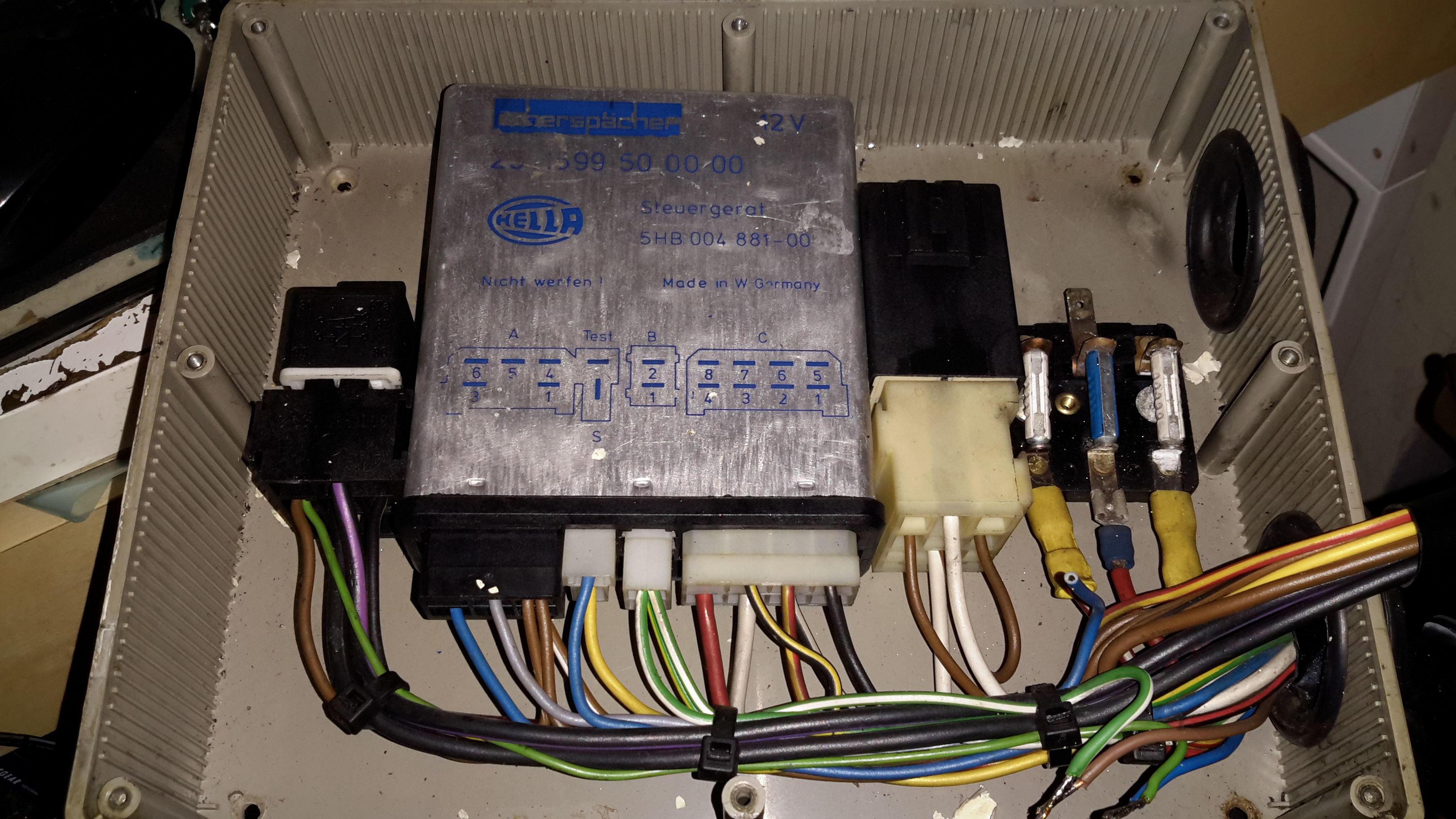
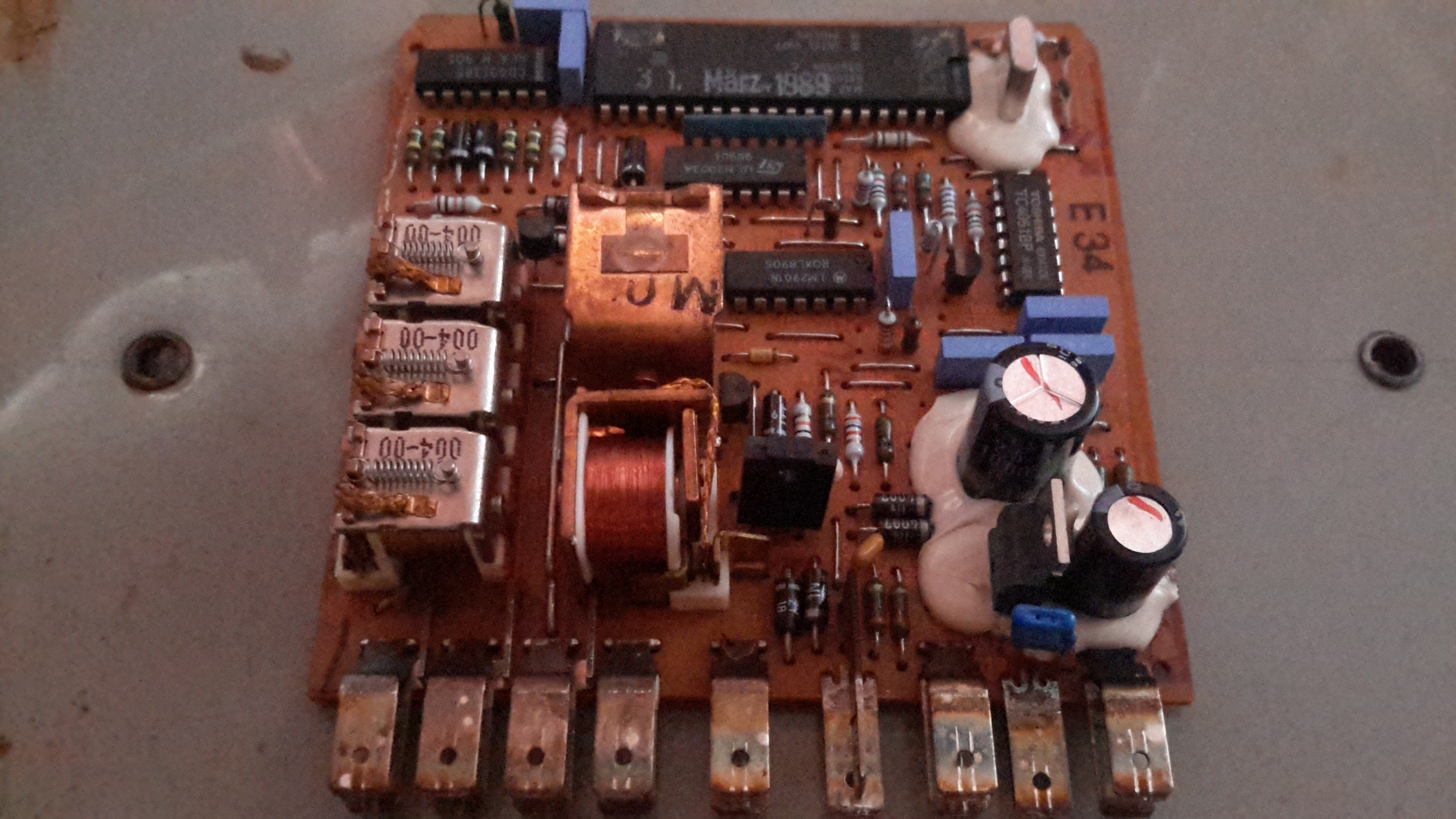
Here’s another Eberspacher control unit, this time from an ancient D5W 5kW water heater. The system in this case is just flaky – sometimes the heater will start without fault & run perfectly, then suddenly will stop working entirely.
The error codes are read on these very old units via an indicator lamp connected to a test terminal. In this case the code was the one for Overheat Shutdown.
Considering this fault occurs when the heater is stone cold, I figured it was either a fault with the sensor itself or the ECU.
Temperature Sensor
The temperature sensor is located on the heat exchanger, right next to the hot water outlet fitting. I’m not sure what the spec is, but it reads exactly 1KΩ at room temperature.
ECU PCB
The PCB is held into the aluminium can by means of crimps around the edge that lock into the plastic terminal cover. Inserting a screwdriver & expanding the crimps allows the PCB to be slid out.
Casing Crimps
The factory date stamp on the microcontroller dates this unit to March 1989 – considerably older than I expected!
Unlike the newer versions that use transistors, this ECU has a bunch of PCB relays to do the high current switching of the water pump motor, fan motor & glowplug.
Overall the board looks to be solidly constructed, with silicone around all the larger components.
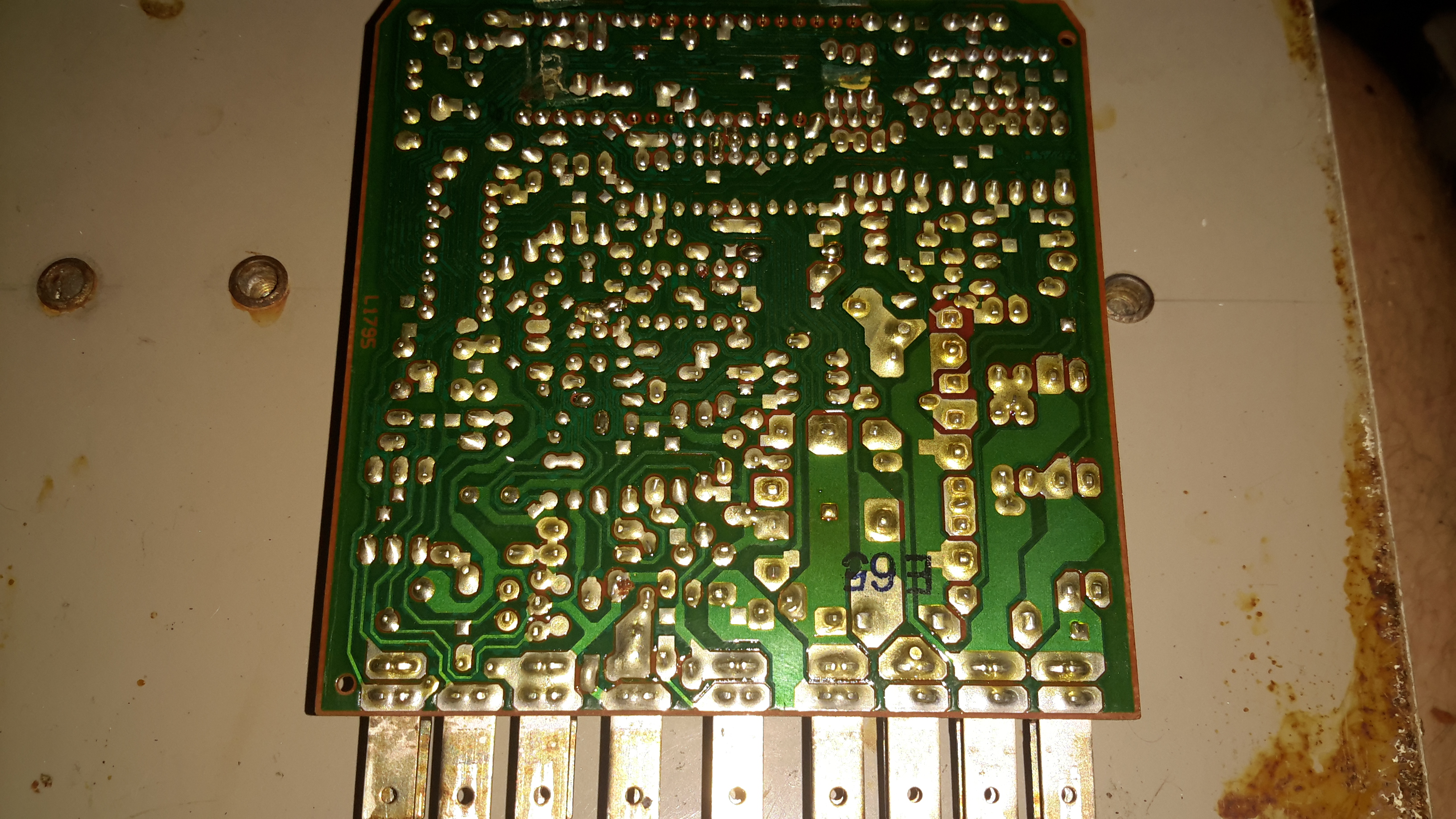
ECU PCB Solder Side
Here’s the solder side of the PCB, which has a generous coating of sealant to keep moisture out.
Bad Joint Closeup
Looking at the solder joints for the row of relays on the top side of the PCB, it looks like that there’s some dry joints here.
I suspect that years of vibration has taken it’s toll, as the relays are otherwise unsupported. It wouldn’t be possible to use silicone to secure these devices as they are completely open – any sealant would likely stop them from operating.
Resoldered Joints
Using a very hot soldering iron I managed to get the joints to reflow properly, using lots of flux to make sure the conformal coating didn’t interfere with the reflow.
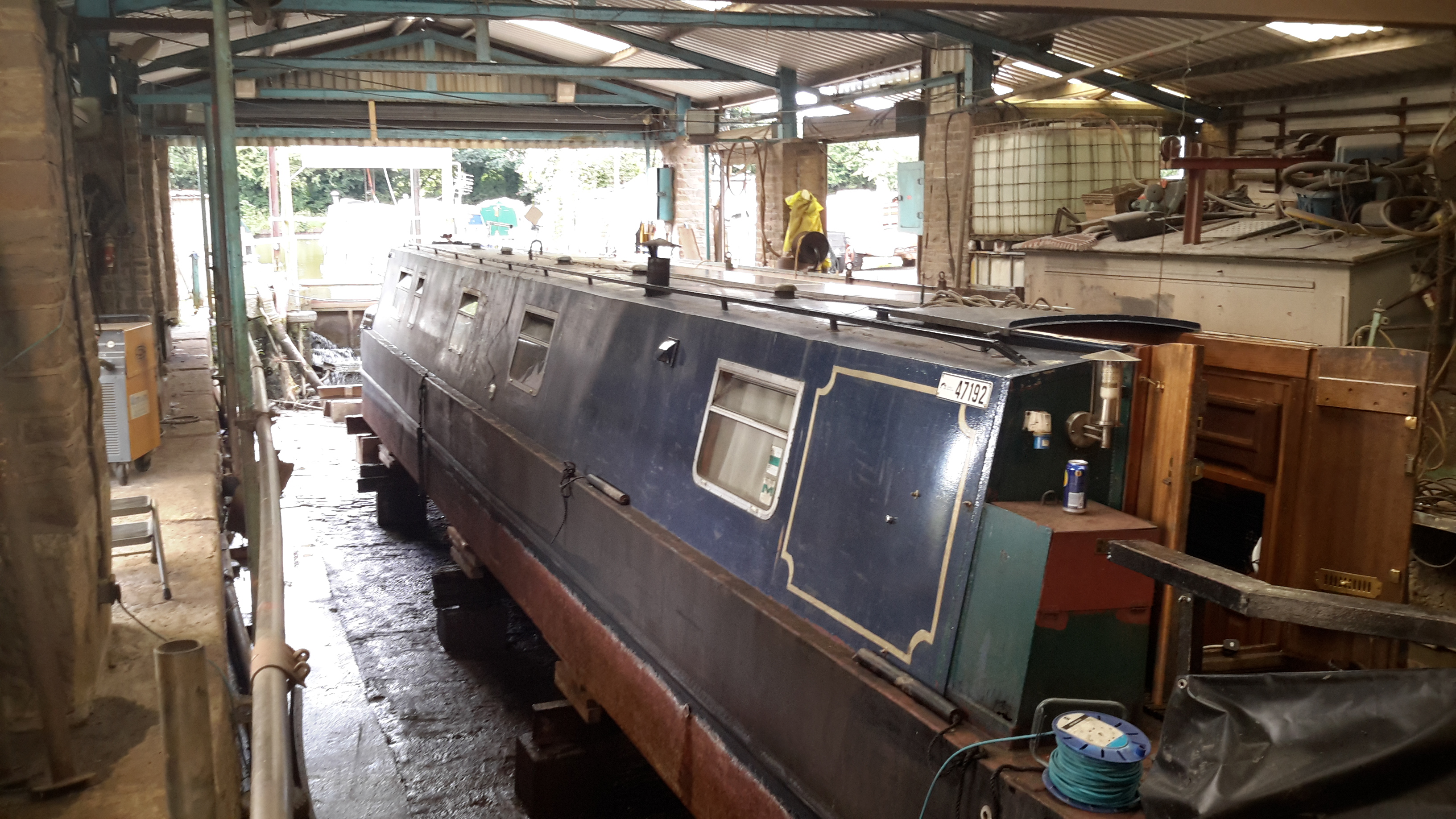
It’s that time again, so the boat is out of the water for it’s 3-yearly maintenance. Some things over the past few months have been bugging me, namely a pronounced vibration in the running gear while underway. (Issue was easy to spot here!).
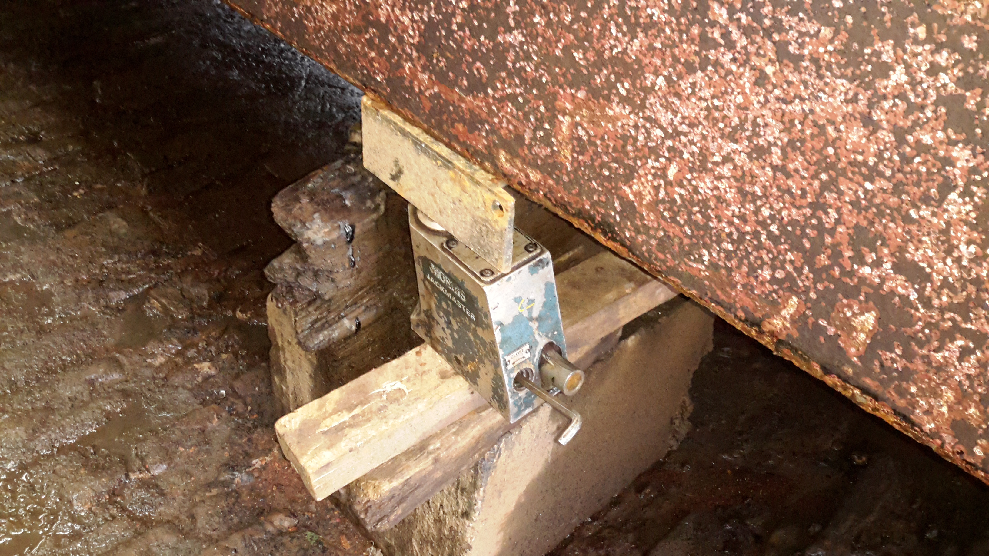
10-Ton Jack
nb Tanya Louise being a very odd vessel, she has quite a significant keel, so once the dock was drained, some manual jacking was required to get her level on the blocks. Without this extra work there is such a pronounced heel that it’s impossible to do anything on board.
Chocks
On the opposite side, wooded blocks are placed for the bottom of the hull to rest against. Jacking up a 58-ft 25-ton boat by hand onto some timbers was nerve-wracking to say the very least!
The bottom of the hull has already been jet-washed to remove 3-year’s worth of slime, weed growth & the old blacking. First job is to get a fresh coat of paint on.
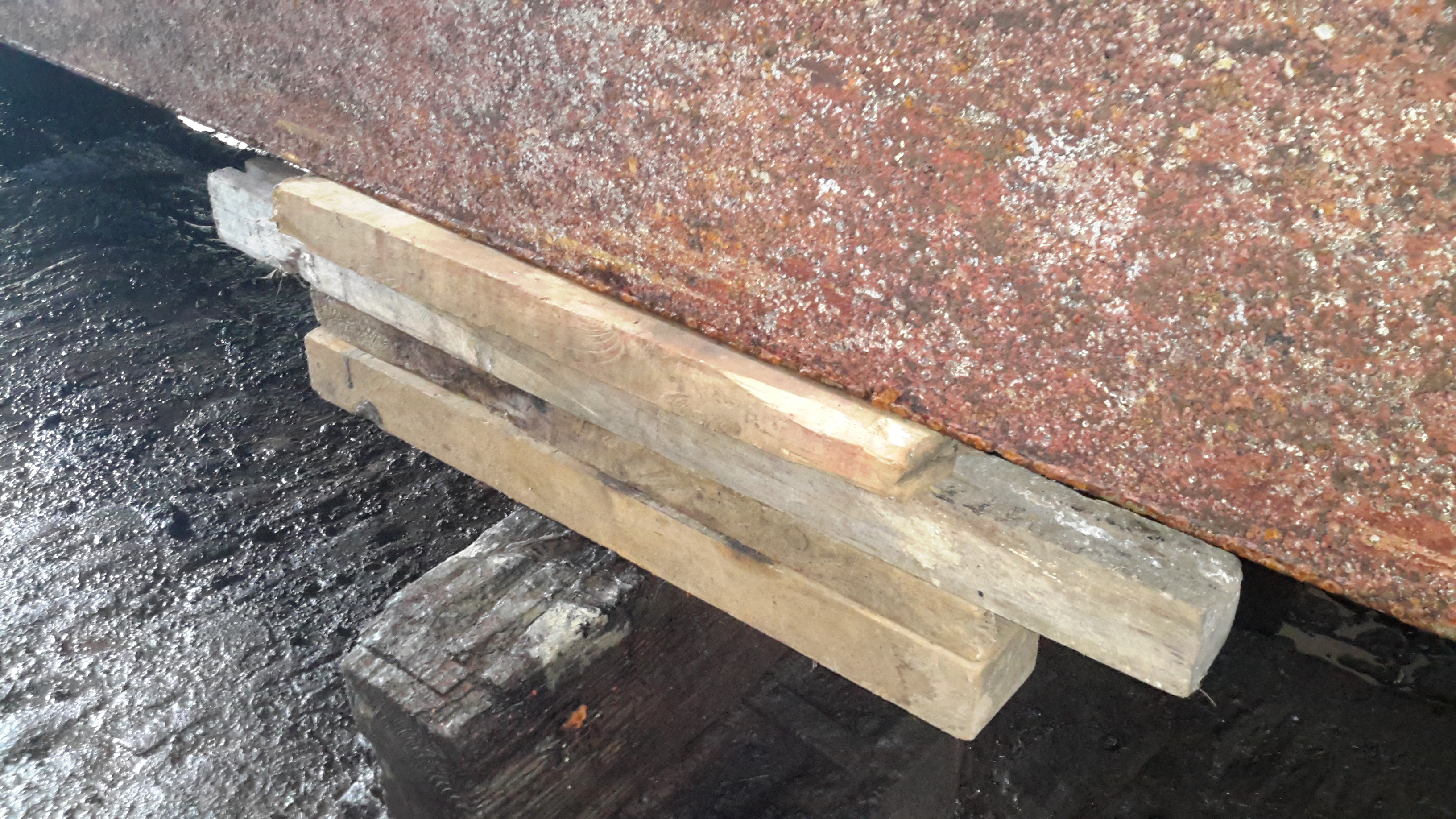
Running Gear
Looking under the hull shows the reason for the high level of vibration – the prop shaft has actually *worn through* the bearing & stern tube, to the extent that there’s not much left of the assembly! The only thing holding the shaft in place at this stage is the stuffing box inside the boat & the shaft coupling to the hydraulic motor.
, stern tube,
A replacement standard-issue Cutless bearing will be fitted, after the remains of the old tube are cut back to make room. To facilitate mounting the bearing, a custom stainless P bracket is being made at a local engineers, for me to weld onto the bottom of the hull.
(Surprised we didn’t lose the shaft, lucky that I kept pestering to get her out of the water!).
Recently my phone decided it was going to die a battery-related death, and having not found much useful information on the Great Google, (all the information I could find, was hinting at many issues from firmware to a faulty motherboard, nobody seems to have actually done any investigation into similar issues), I decided to dig into the phone to try & repair the problem.
Broken Flex
The phone would work correctly for a while, then with the slightest movement or knock, would spontaneously switch off, and not turn back on without being whacked on a hard surface.
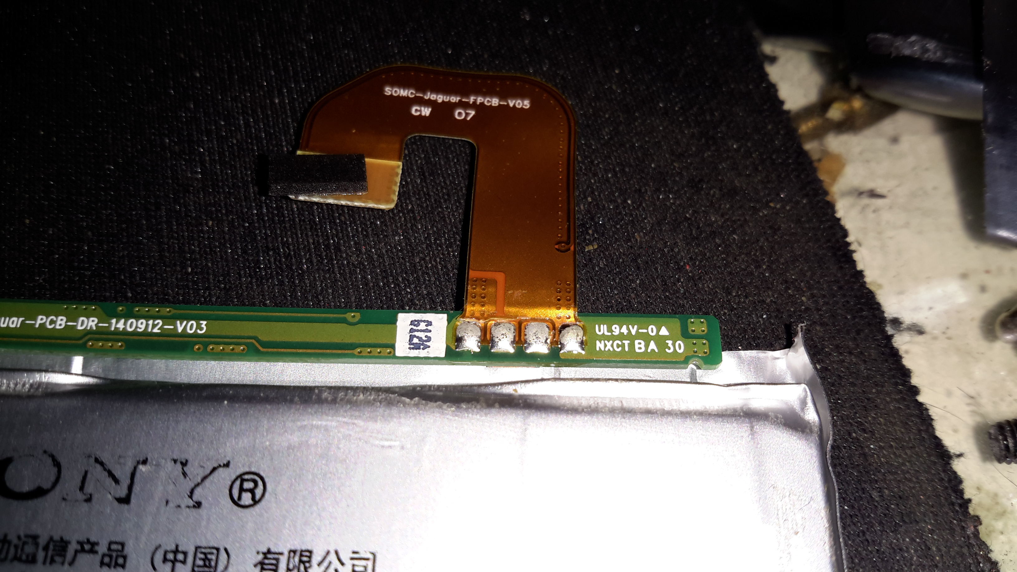
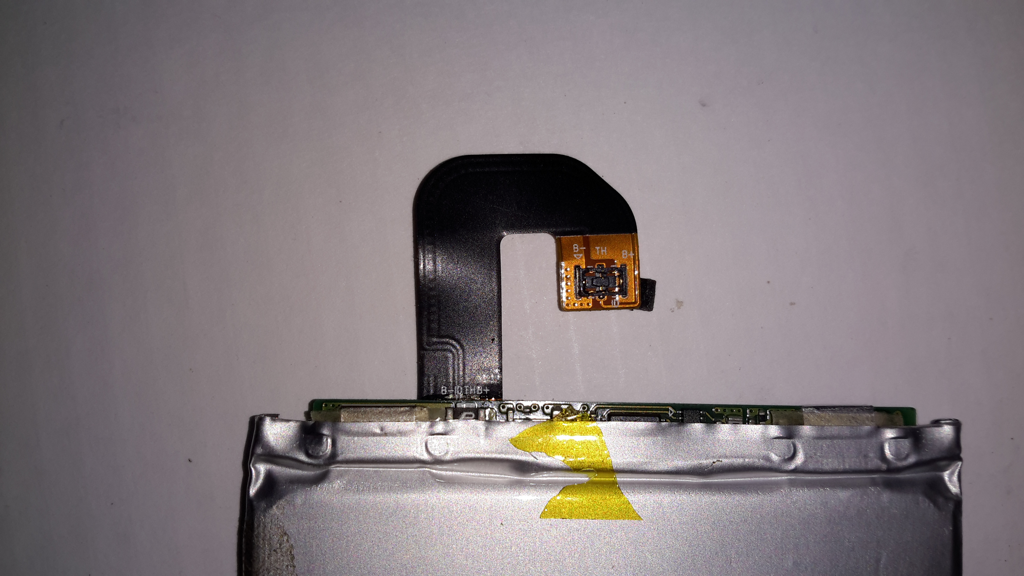
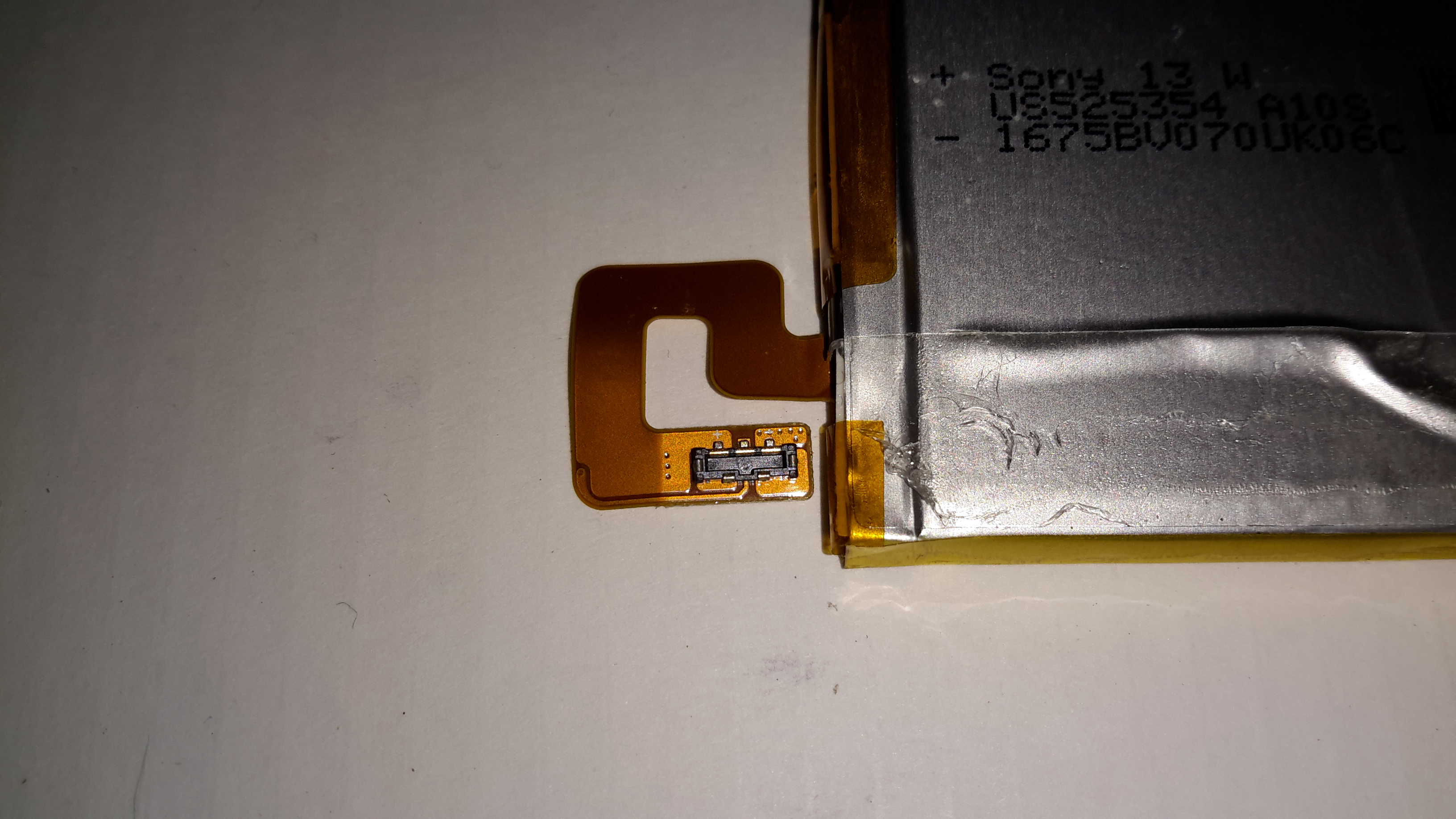
This symptom pointed me at a power connection problem. After removing the back of the phone (glass & heavily glued in place, so an awkward process), This was what I was presented with on the cell flex PCB.
In the above photo, the positive connection to the flex is fractured just after the solder joint with the BMS board.
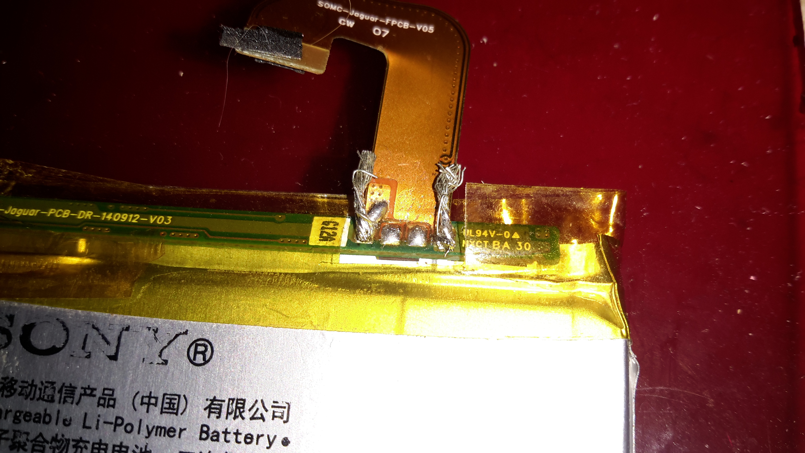
Flex Repair
I managed to scrape some of the insulation off the flex PCB & solder a jumper on to restore power. Unfortunately, this repair generated another fault, where the battery level was always shown at 50%, and plugging into a USB supply wouldn’t charge the phone. The other two pins on the cell are for communication & temperature sensing, clearly one of these traces was also broken in the flex.
The above photo has a pair of very small wire tails as well, for connecting an external charger.
50% Battery
Here’s a screenshot of the phone with the original cell, even though it’s at about 4.15v (virtually fully charged). The battery management is having trouble talking to the phone, so for safety reasons, the charging logic refuses point-blank to charge the thing up.
Flex Cable
The connector on the cell & phone motherboard is absolutely tiny, so I didn’t fancy attempting to solder on any bridge wires to try & bypass the broken flex.
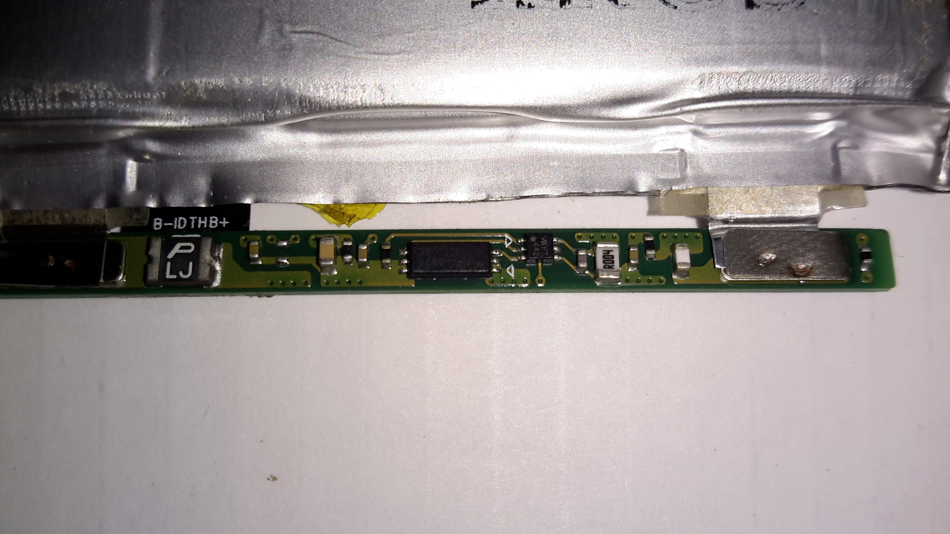
Battery BMS
The cell BMS has some intelligence on board, besides the usual over-current, over-charge & under-charge protection. The very small IC on the right has a Microchip logo, and the marking FT442, but I was unable to dig up any datasheets. The current sense resistor is directly connected to this IC, along with the main power FET to the left.
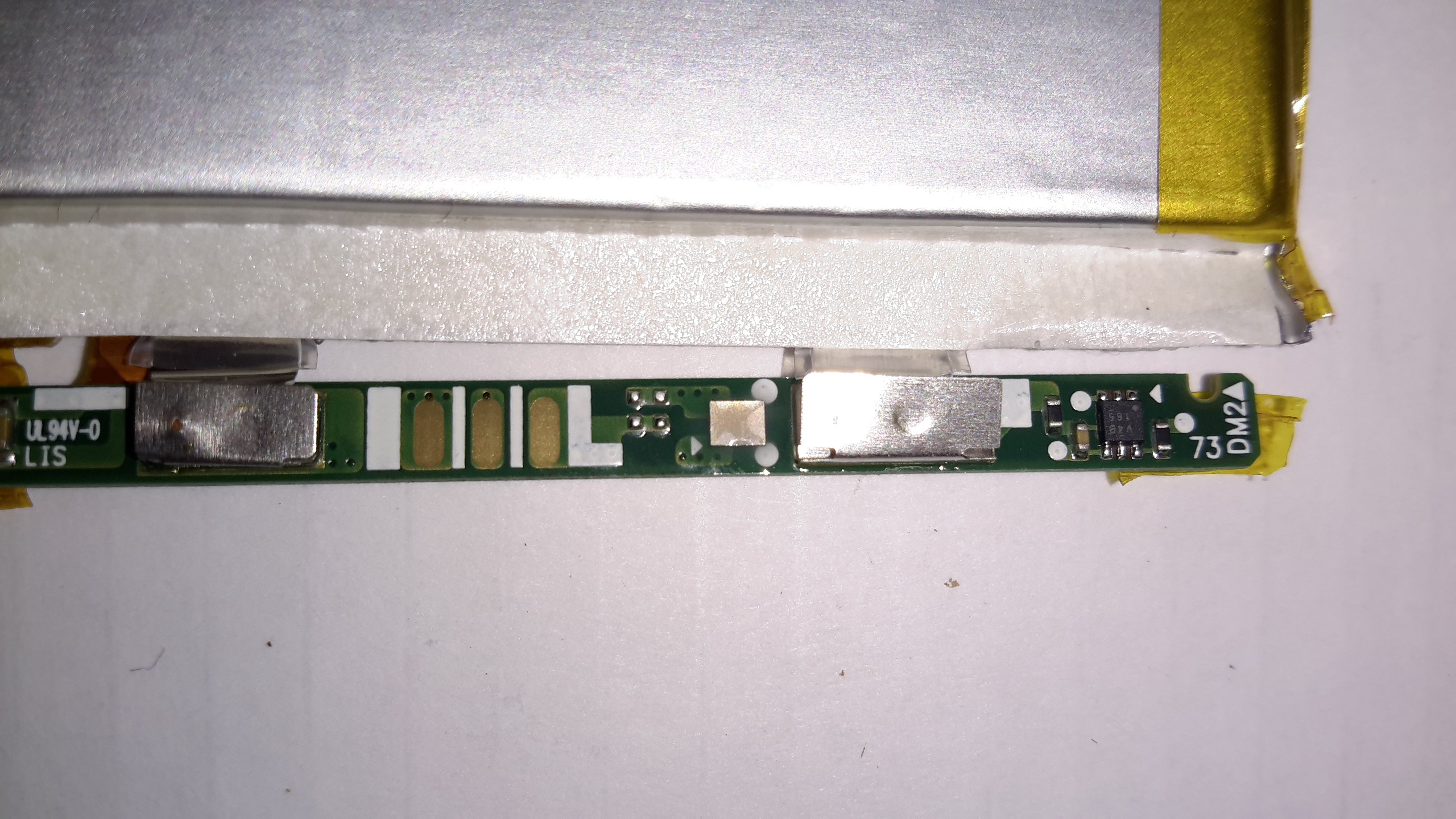
BMS Reverse
On the other side of the BMS board is another IC, again unidentifiable, and what looks like a bare-die, or CSP IC.
At this stage I figured the only way forward was to buy a new battery, eBay turned one up for less than £5. Above is the new battery fitted to the phone, datestamped 2014, so definitely old stock.
100% Battery
Booting the phone with the new battery quickly lets me know the fix worked, with a 100% reading & the ability to again charge properly!
Since this phone has been in my drawer for some time, I figured it was time for a teardown. (It’s never going to see any more use).
The back cover on these phones is easily removed, as it’s just clipped on.
Motherboard
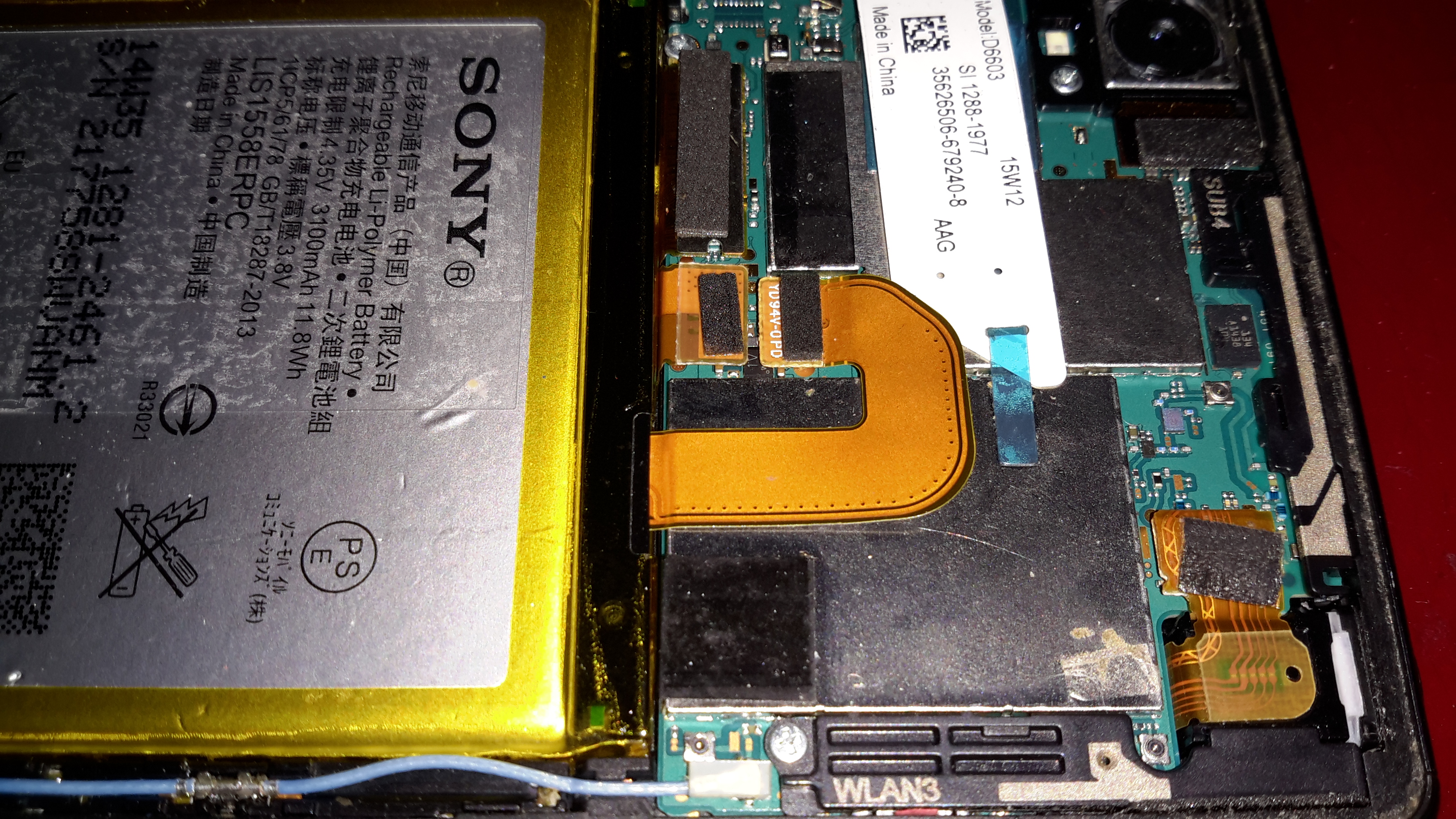
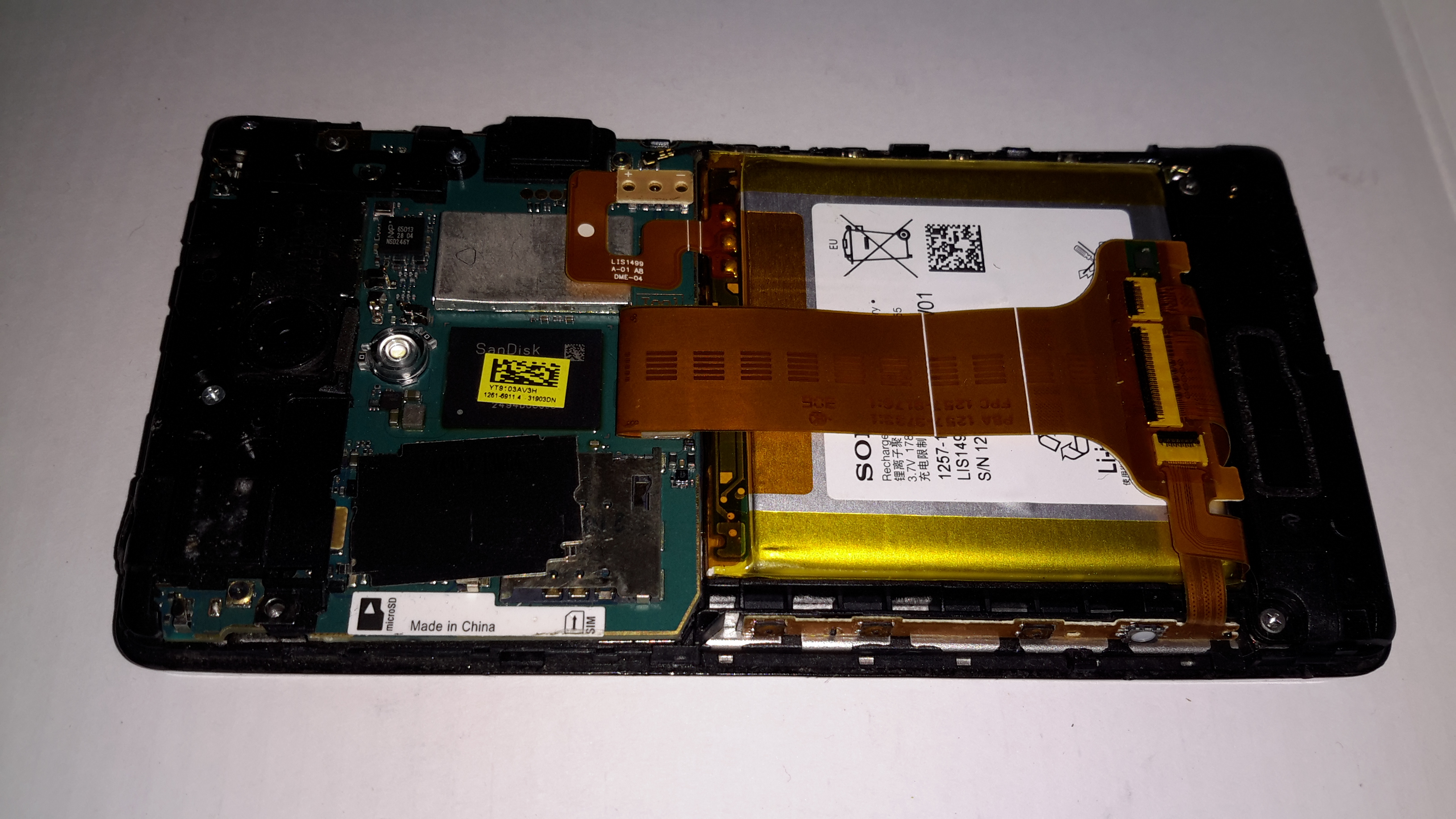
Once the back cover is removed, the Li-Polymer cell is exposed, along with the logic board. Pretty much all of the PCB is under RF shields.
Motherboard RemovedBattery Management
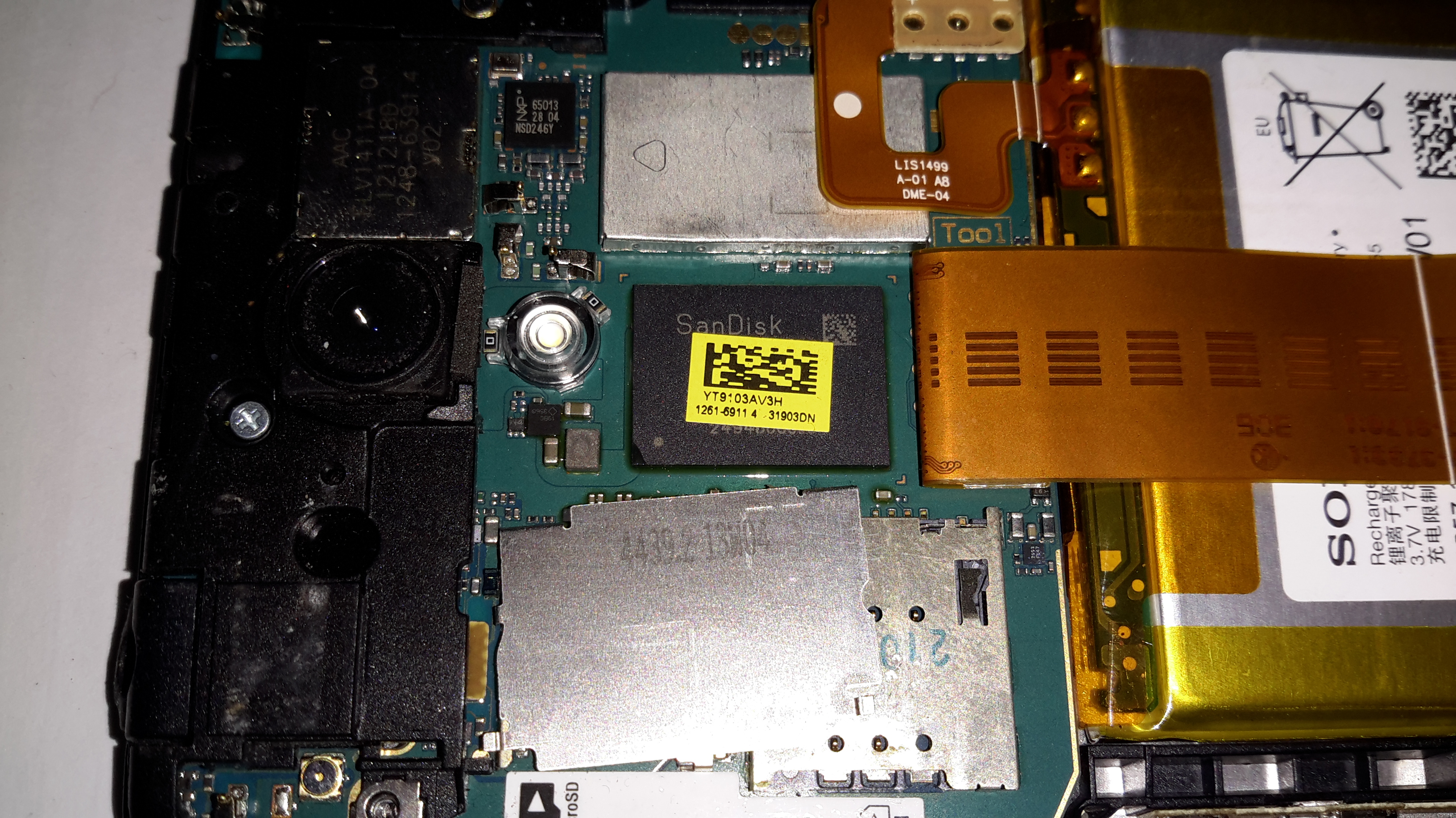
Under the small RF can on the back of the board is the battery management circuitry & the charger. There’s an extra connection to the cell for temperature monitoring. Just under that circuitry is the eMMC flash storage.
Just to the left of the battery circuit is the NFC transceiver IC, from NXP.
Battery Flex
The cell is connected to the main board with a FFC, with a very small SMT connector, although not as small as the more modern Xperia series phones.
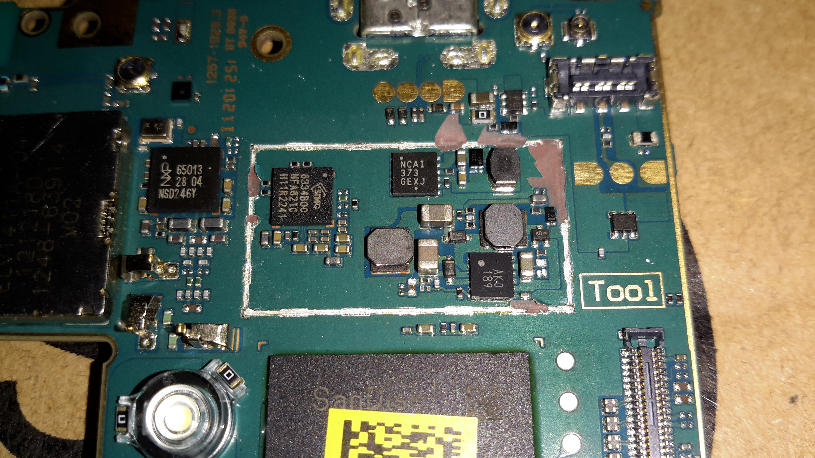
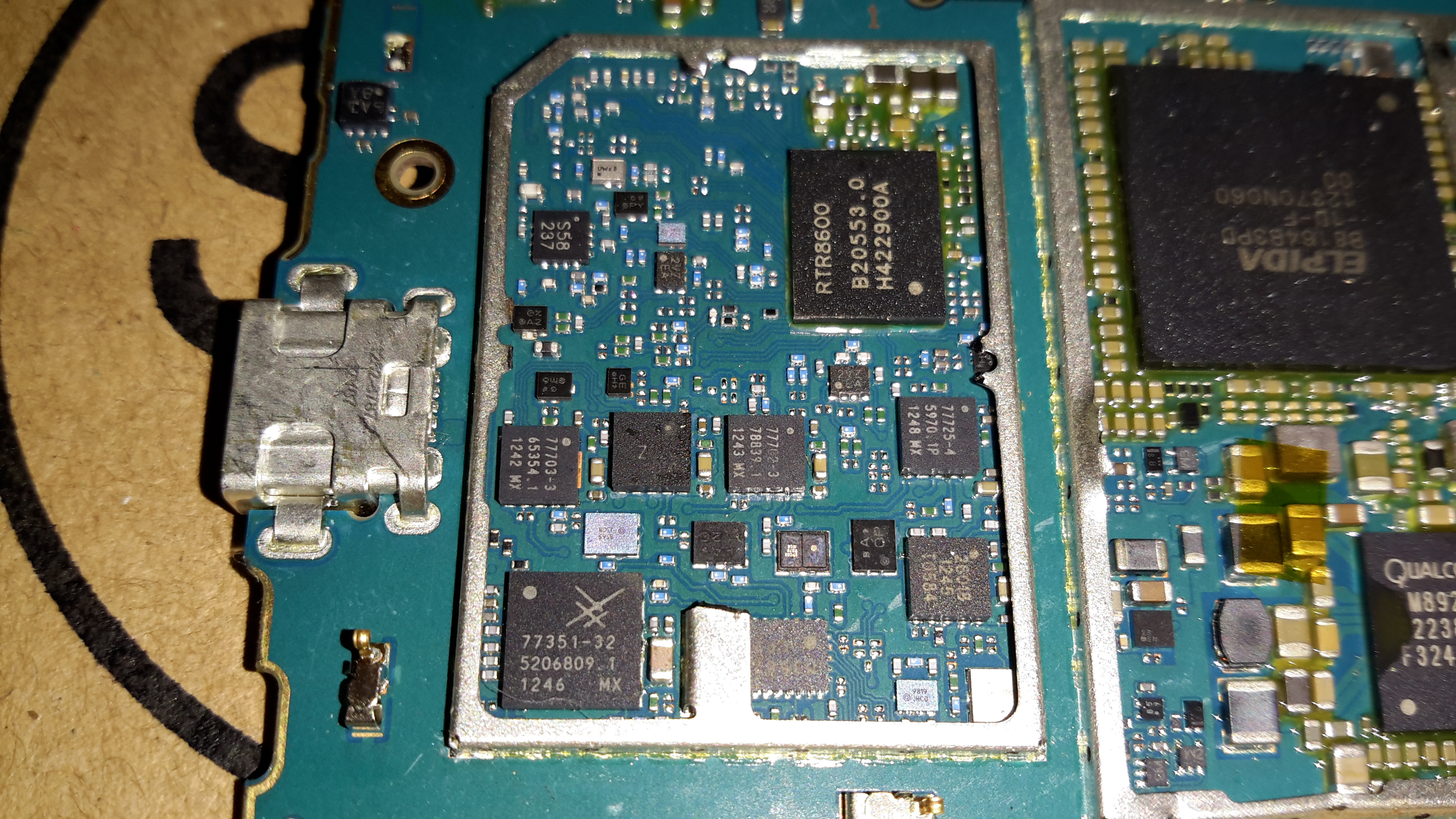
RF Section
The other side of the mainboard holds the large RF transceiver section, with a Qualcomm RTR8600 multiband transceiver IC. In the bottom corner is a Skyworks SKY77351-32 Quad-band power amplifier IC, along with 3 other power amplifier ICs, also from Skyworks.
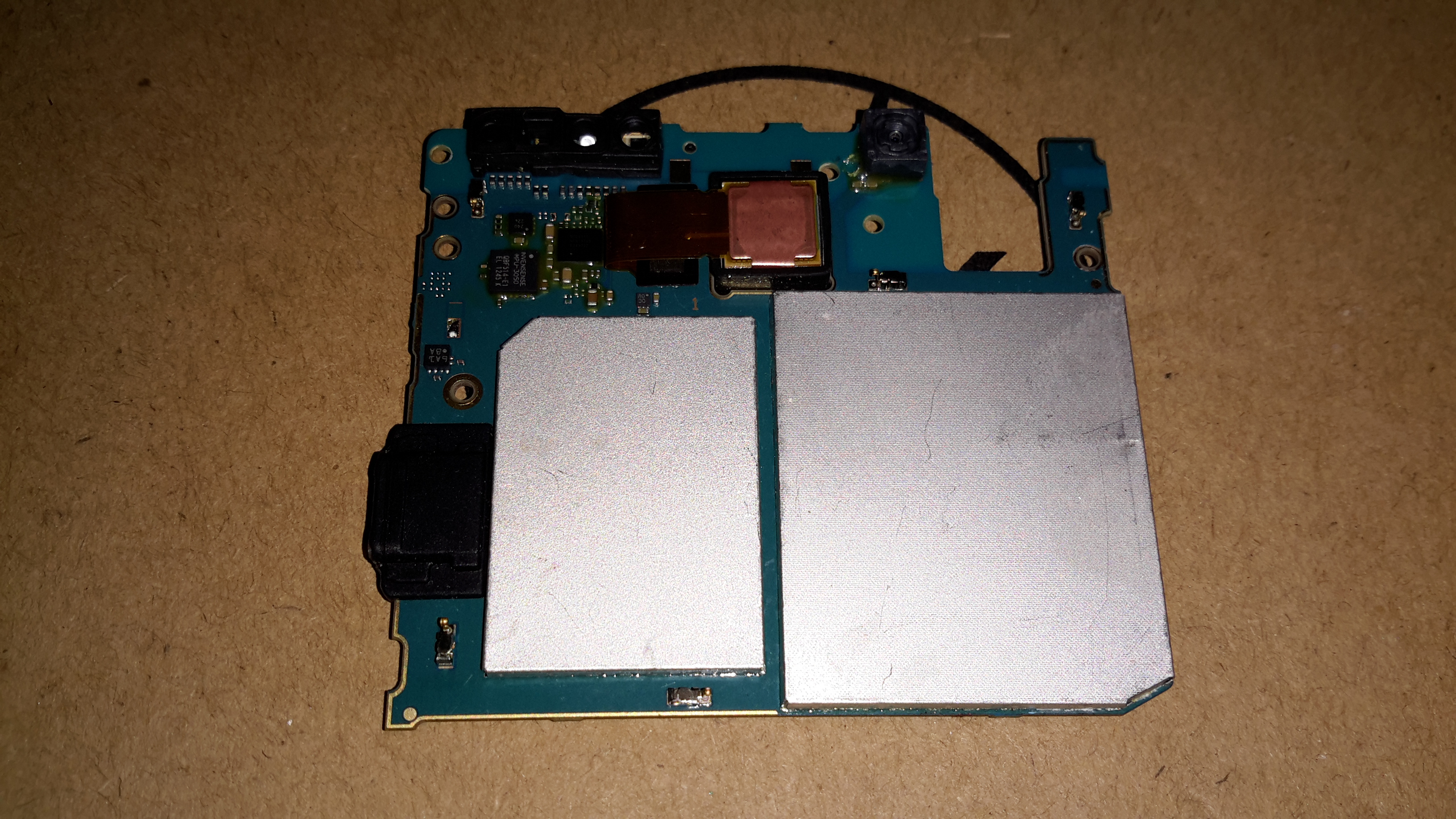
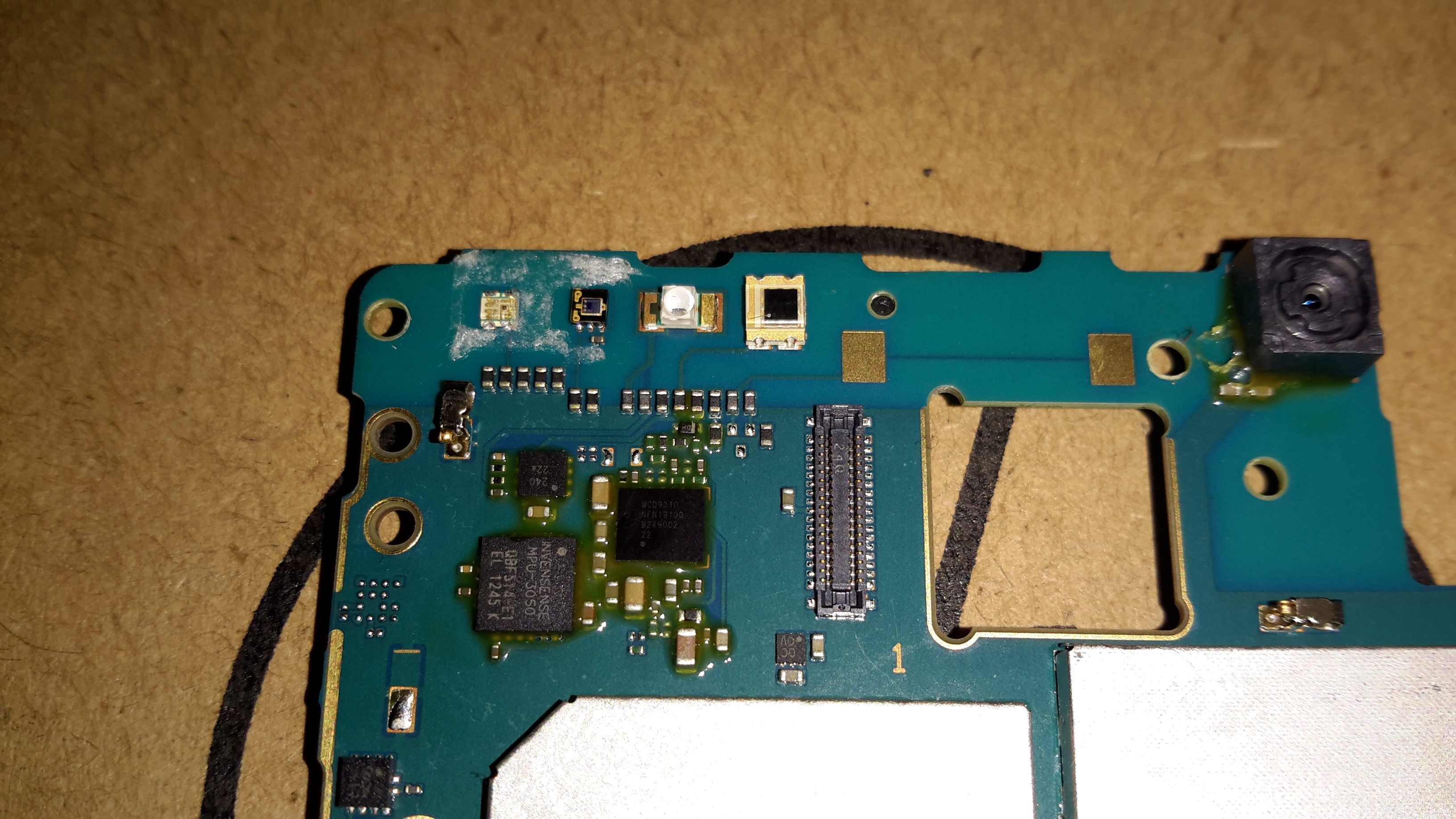
Gyro & Audio Codec
The top corner of the board holds the various sensors, including an Invensense MPU-3050 3-axis gyro. To the right of that is the Audio Codec, a WCD9310 from Qualcomm.
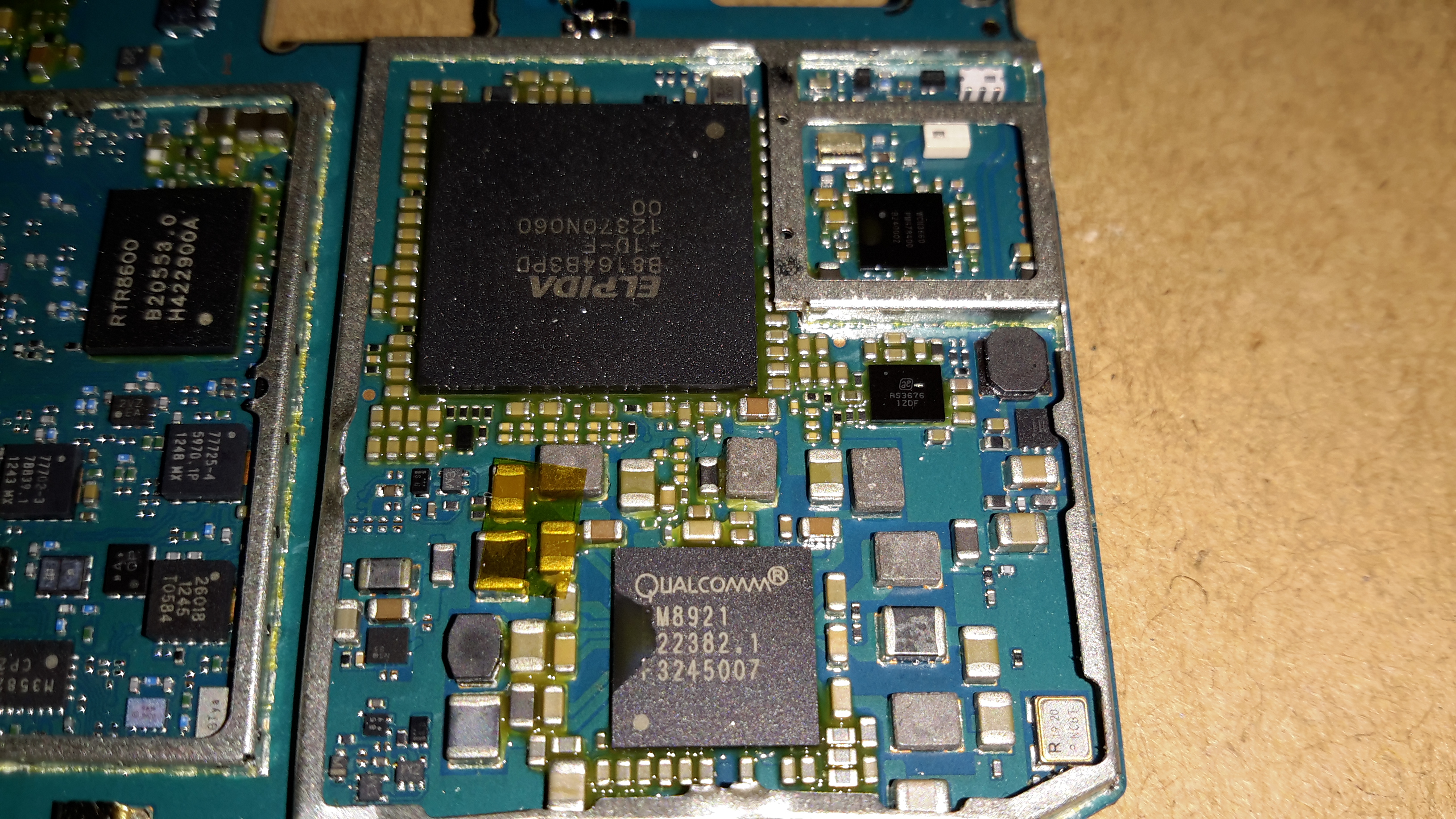
Logic & CPU Section
Everything is controlled from the last section on the board, with the main CPU & RAM in a PoP (Package-On-Package) configuration. Under the main CPU is the main power management IC, also from Qualcomm. No datasheet for this one unfortunately, but it gives it’s purpose away by being surrounded by large inductors & capacitors.
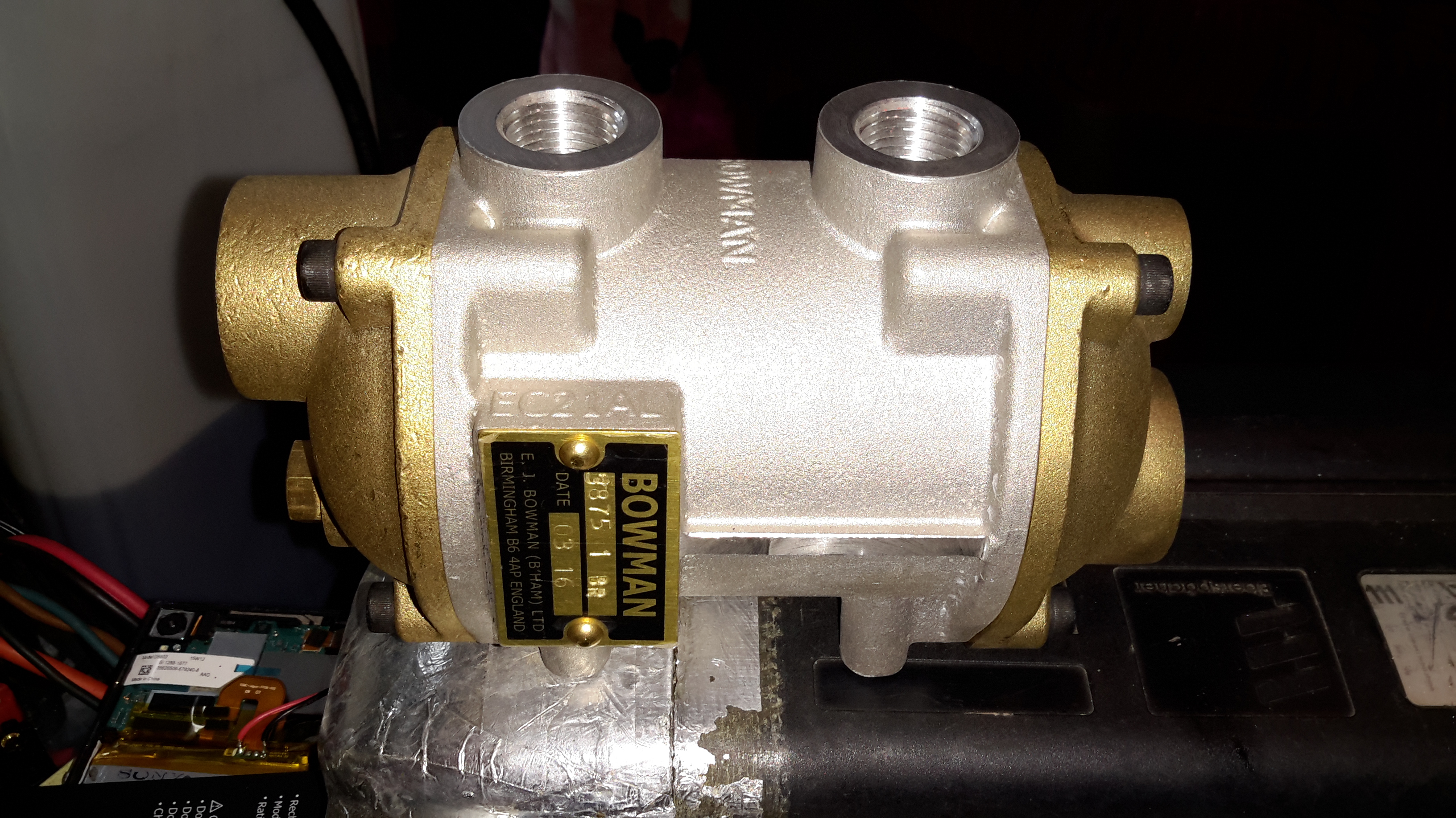
To solve some engine oil overheating problems on board nb Tanya Louise, we decided to replace the air-over-oil cooler, with an water-over-oil cooler, with separate cooling drawn straight from the canal, as the skin tanks are already overloaded with having to cope with not only cooling the engine coolant, but also the hydraulic system oil as well.
These units aren’t cheap in the slightest, but the construction quality & engineering is fantastic.
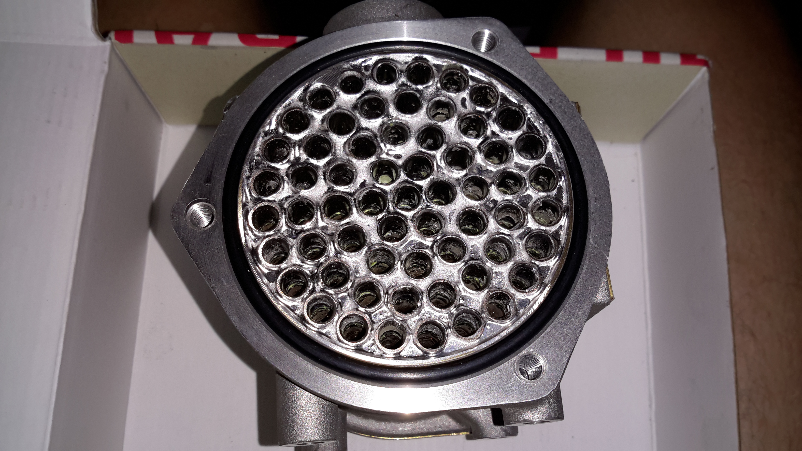
Tube End Plate
Unbolting the end cover reveals the brass tube end plate, soldered to all the core tubes in the cooler. An O-Ring at each end seals both the end cover & the interface between the tube plate & the outer casing.
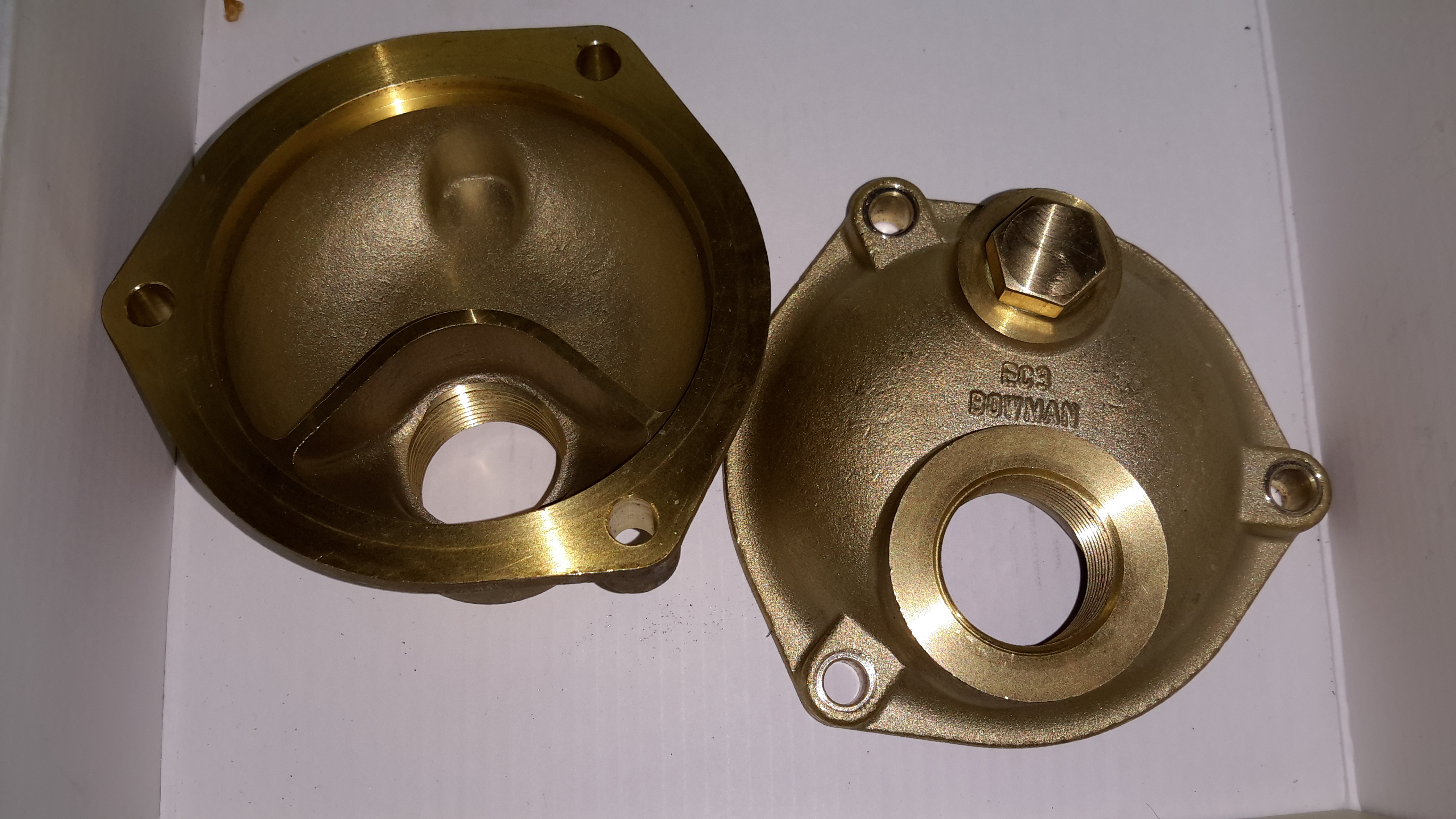
End Caps
The end caps have baffles cast in to direct the cooling water in a serpentine path, so the oil gets the best chance at dissipating it’s heat to the water.
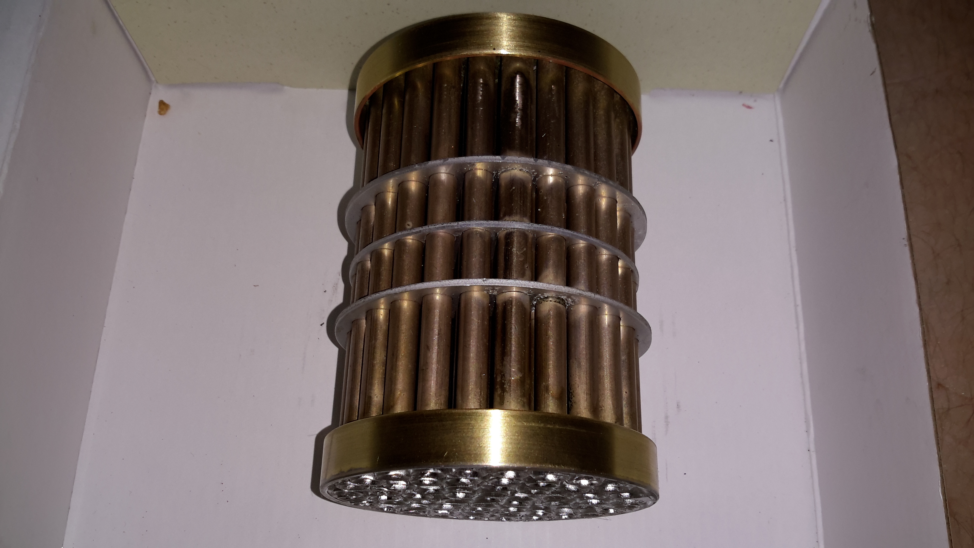
Tube Stack
The oil side of the system is on the outside of the tubes, again baffles placed along the stack direct the oil over the highest surface area possible.
Outer Shell
The outer shell is just a machined alloy casting, with no internal features.
This is something I’ve never seen before. Yesterday, on the Lower Peak Forest Canal, a bunch of kids on off-road bikes came thundering down the towpath – one even pulled a wheelie.
There’s considerable motion blur in the photos, as they were doing some speed, at least 30MPH at that stage.
I did get significant verbal abuse of them for having a camera on them, but thee didn’t bother stopping. This happened at the Romiley side of Woodley Tunnel, just past the portal.
As some will know, I’ve just returned this week from Download Festival, after the yearly pilgrimage to the Mecca of Metal! Click the image below to take a look at the photo albums!
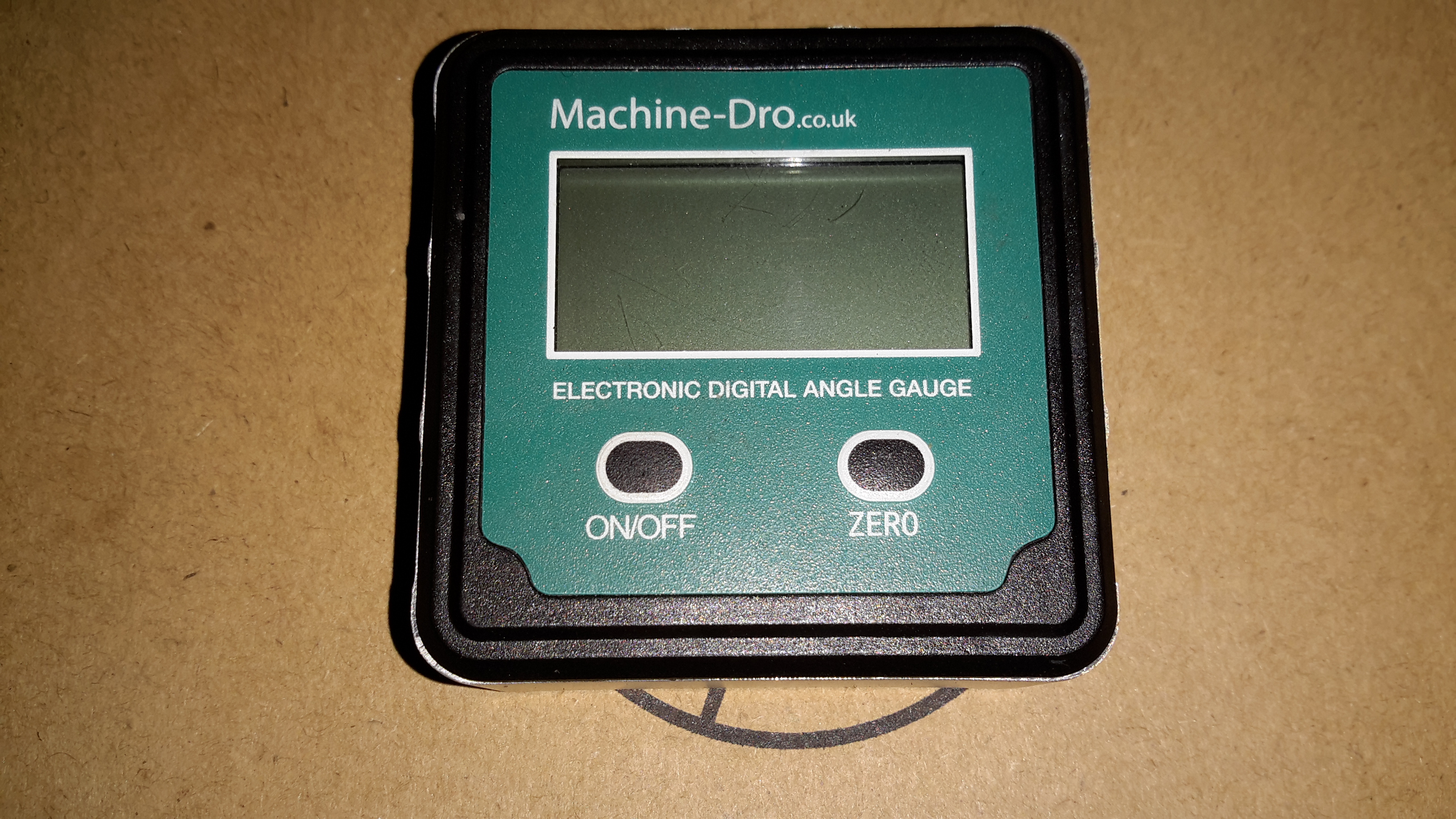
Here’s a useful tool for the kit, a digital angle gauge/protractor. These use a silicon sensor to show the number of degrees the unit is out of level.
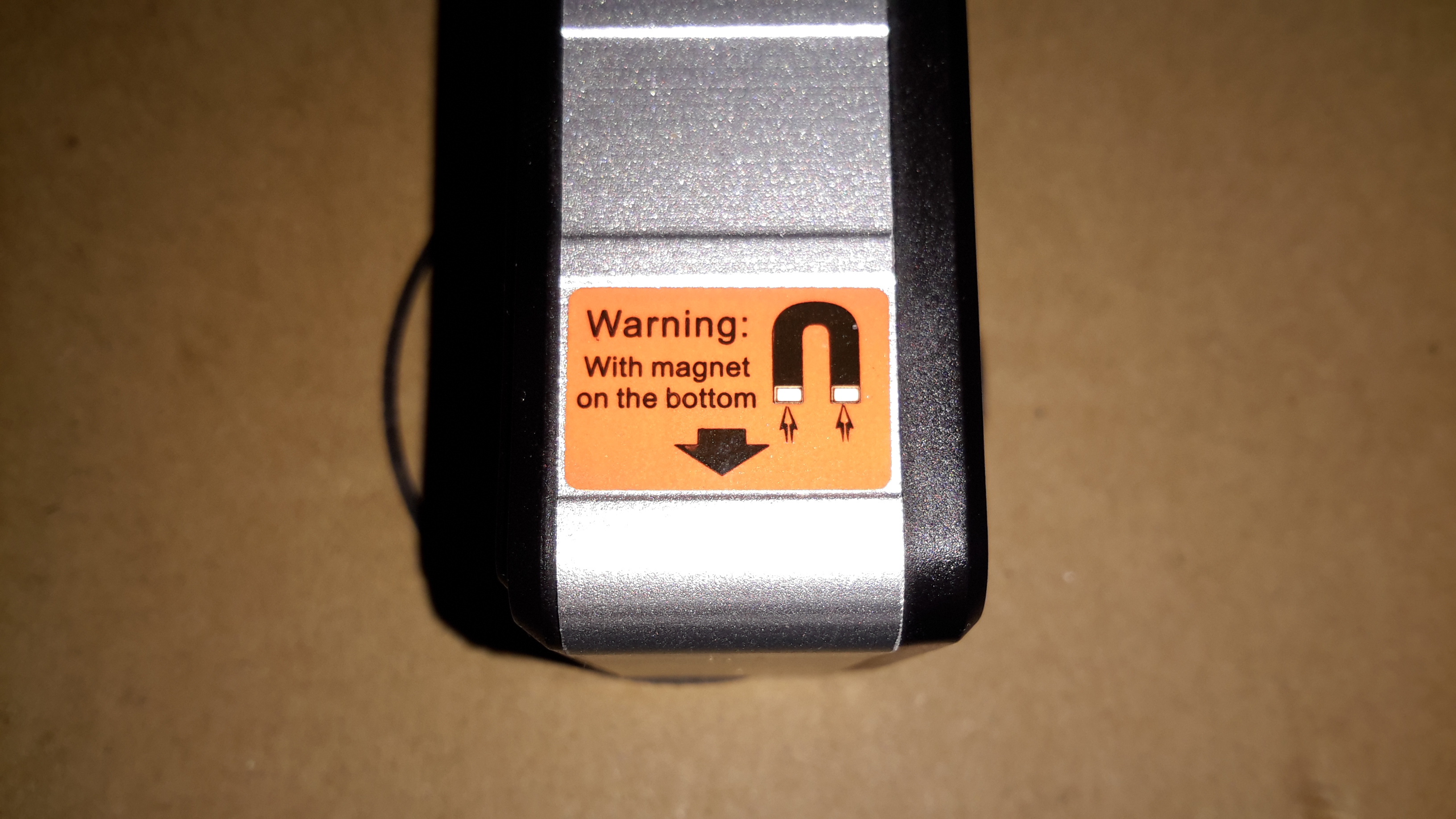
Magnets!
Magnets are provided in the base, so the tool can attach to any ferrous surface.
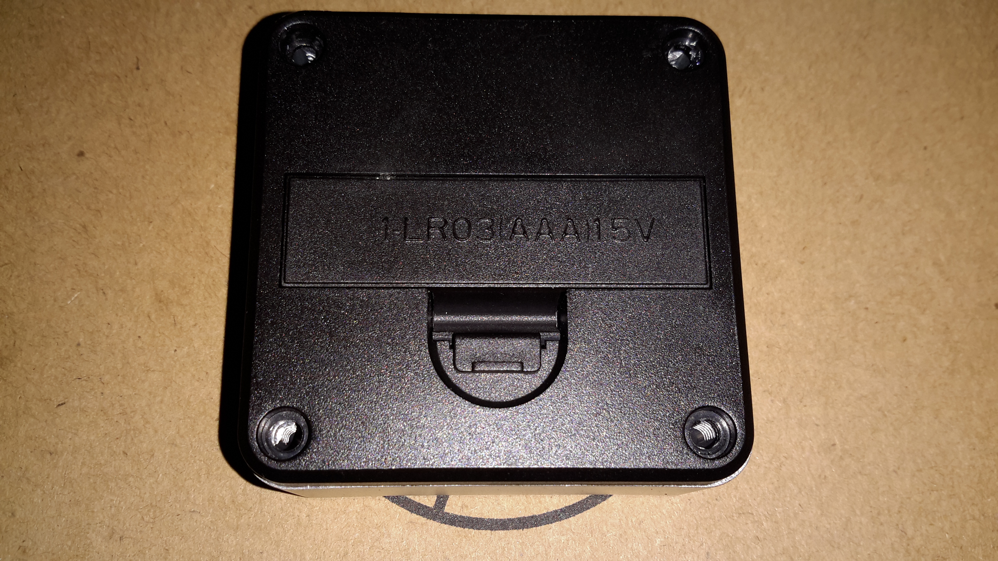
Battery Box
Power is provided by a single AAA cell.
Main PCB
Removing the rear cover reveals the brains of the unit, and there’s not much to it at all. The main microcontroller is a CoB-type device, so no part numbers available from that one.
Sensing Element
The IC to the left of the main microcontroller is the sensing element. There’s no markings on this inclinometer IC so I’m not sure of the specs, but it will be a 3D-MEMS device of some sort.
Power Supply
The other side of the PCB has the power supply for the logic, and a serial EEPROM, probably storing calibration data.
Tip Jar
If you’ve found my content useful, please consider leaving a donation by clicking the Tip Jar below!
All collected funds go towards new content & the costs of keeping the server online.