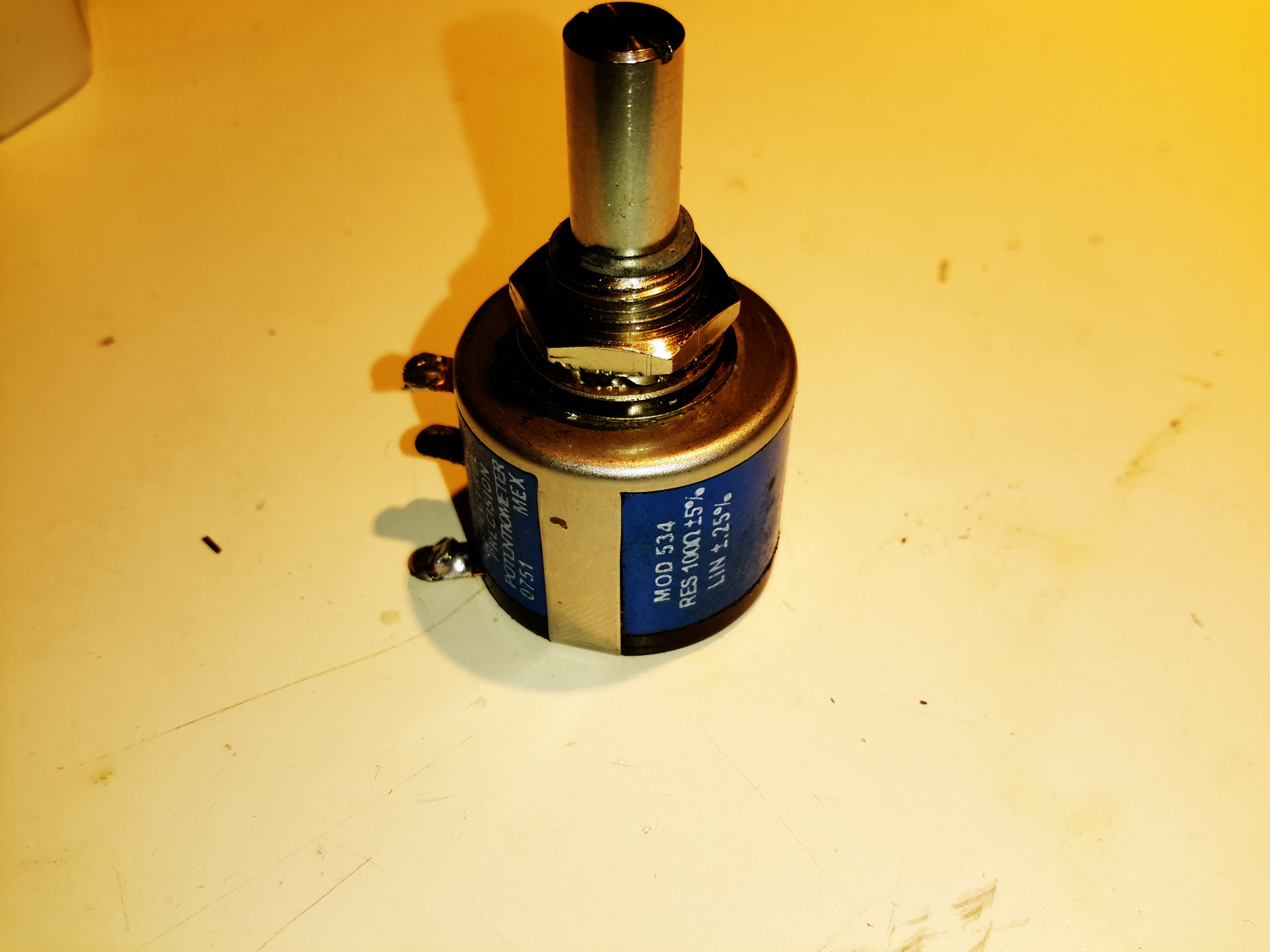
I recently used a Vishay Spectrol Precision 10-turn potentiometer in my latest PSU project, and since these clip together instead of being ultrasonically welded like Bourns potentiometers, I decided to do a quick teardown for the blog. I didn’t find much in the way of how these pots worked from a search, so here we go!
Vishay Spectrol Precision 10-Turn
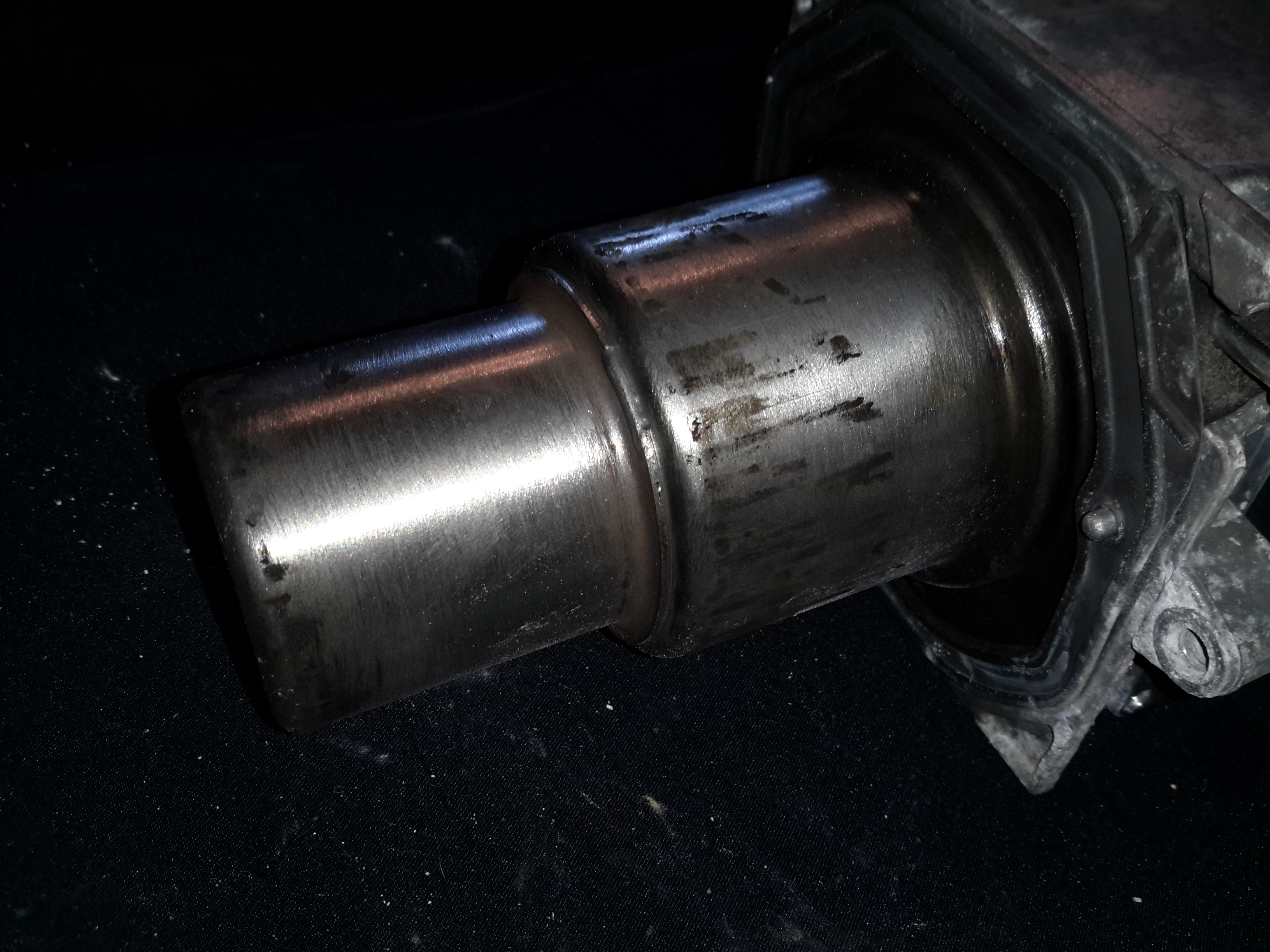
Here’s a pot of the same spec as I used in the previous project, again from my random used junk bin. This is a 100Ω, 5% wirewound potentiometer. The shaft is secured in the centre bushing with a snap ring, this is easily removed with a pair of needlenose pliers.
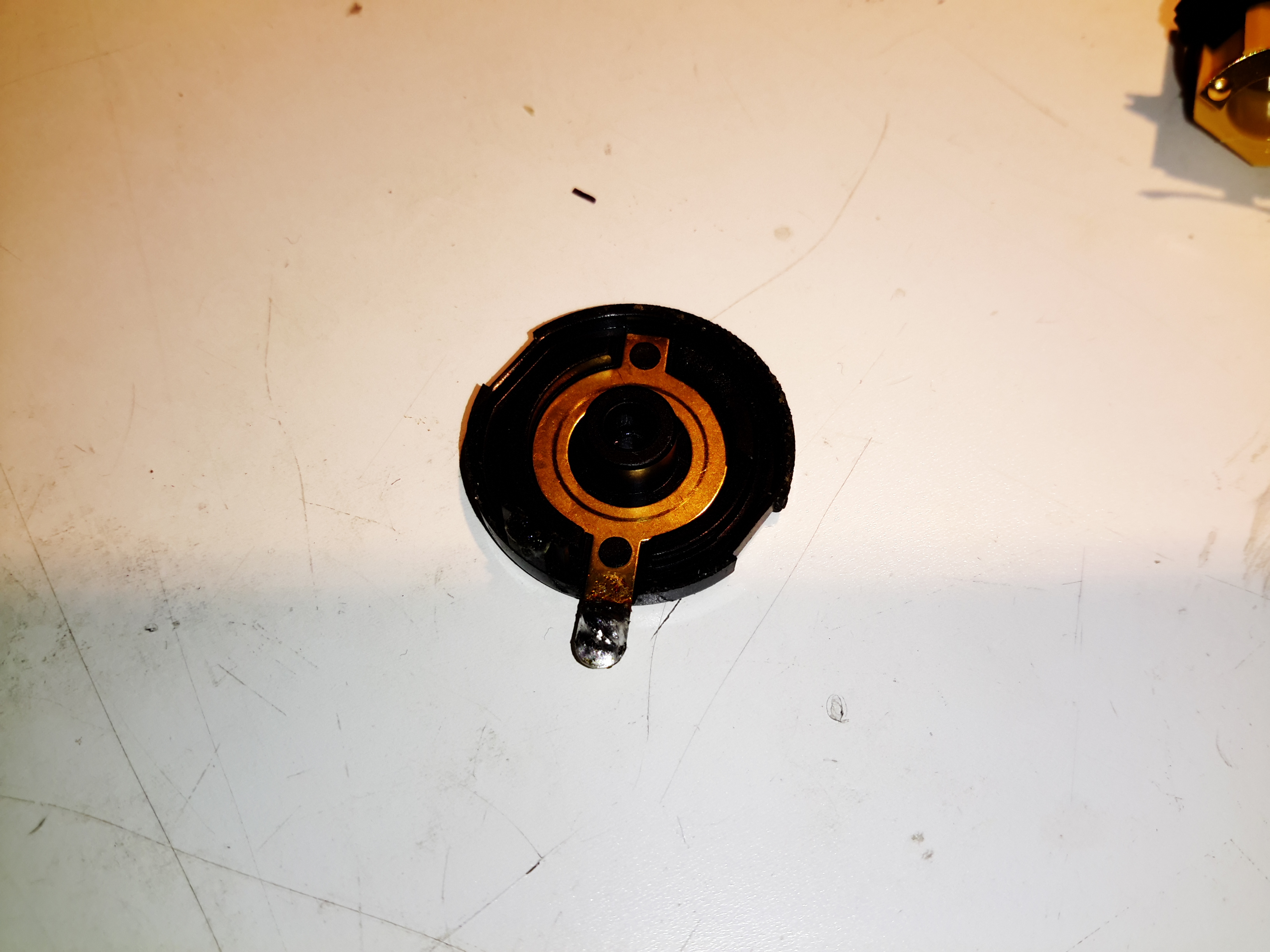
Wiper Stationary Contact
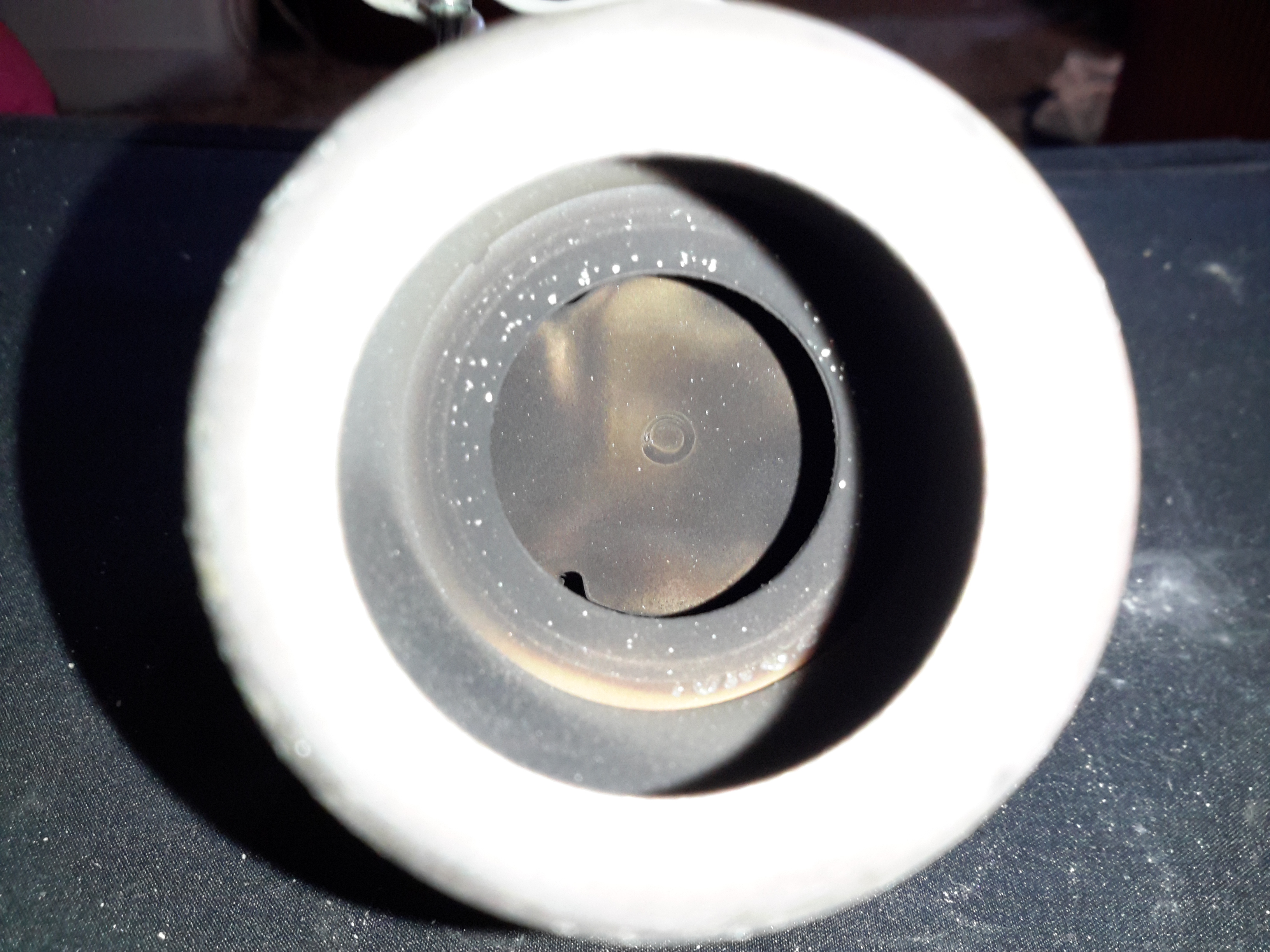
After unclipping the back cover, the stationary part of the wiper contact is visible in the back plastic cover.
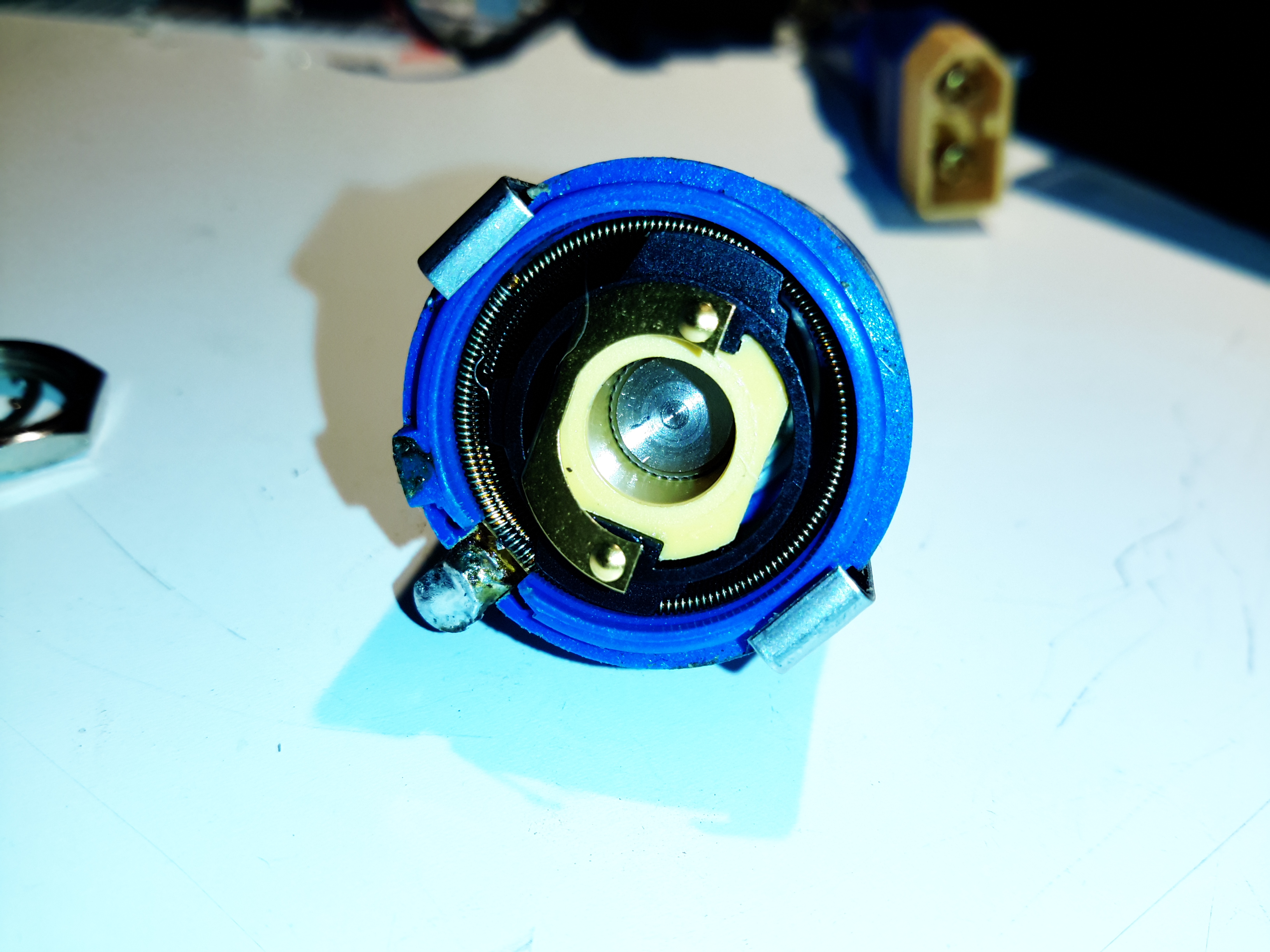
Back Cover Removed
Inside the back of the potentiometer shows the inner workings. These devices have a large helical winding of resistance wire around the inner diameter of the casing, the wiper tracks this helix as the potentiometer is turned.
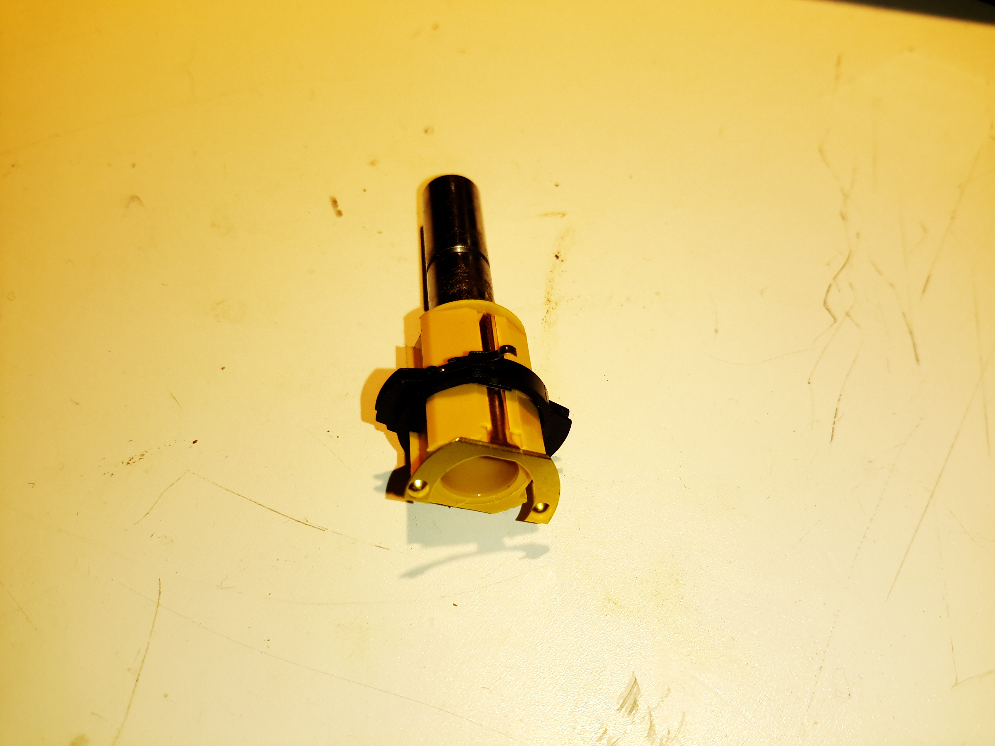
Centre Contact & Shaft
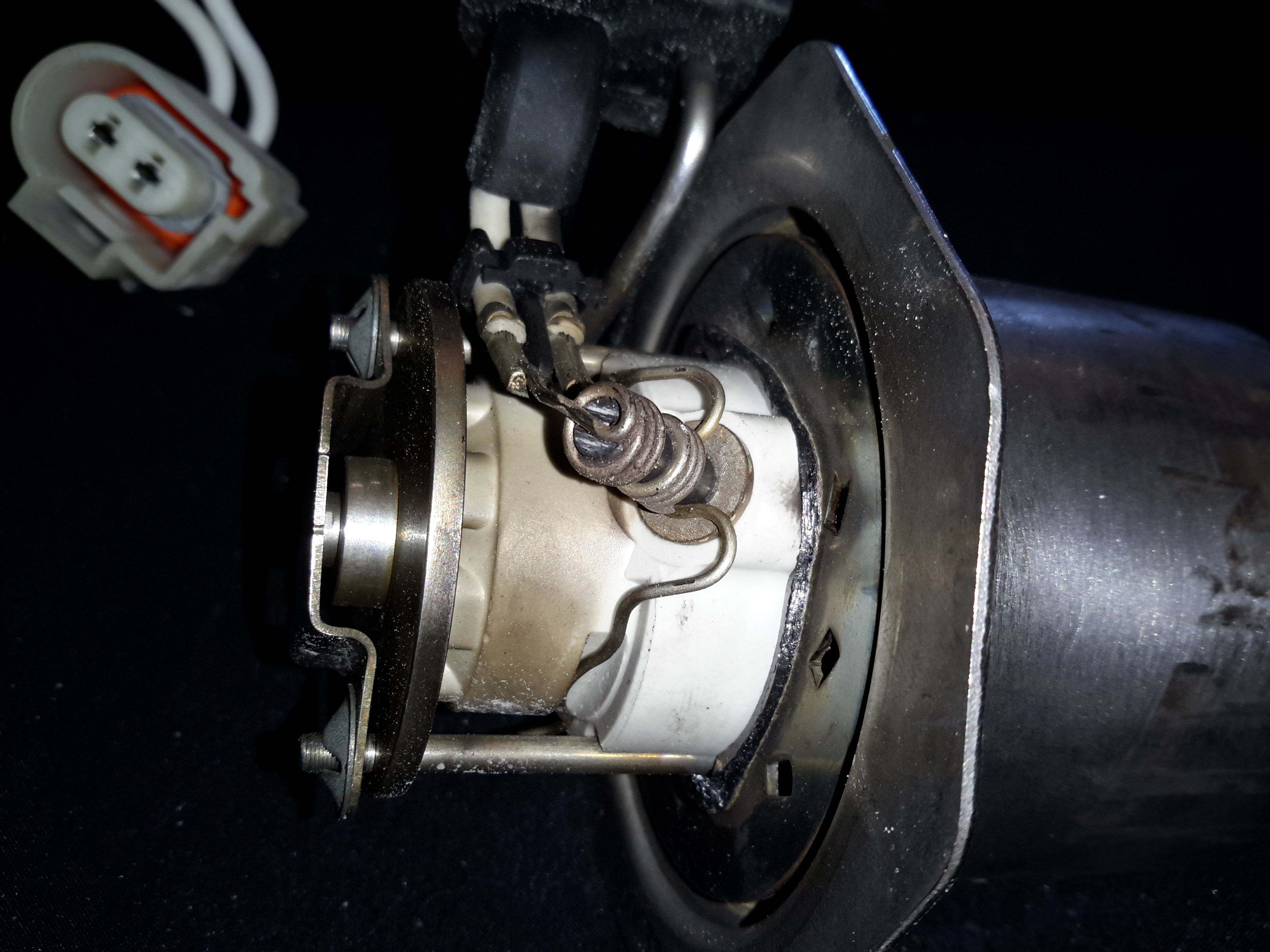
As the wiper must move axially as it winds around the spiral of resistance wire, the contact is mounted on a pair of guides so it can slide back & forth. The electrical connection is made via another spring contact that runs down the side of the plastic shaft insert. Two notches cut into the black plastic wiper frame engage with the round profile of the resistance winding like a screw into a nut, keeping the wiper in perfect alignment as it travels the full length of the winding. I suspect all these moving contacts are made of Beryllium Copper in this rather expensive component as this alloy is very flexible, as well as being a very good electrical conductor.
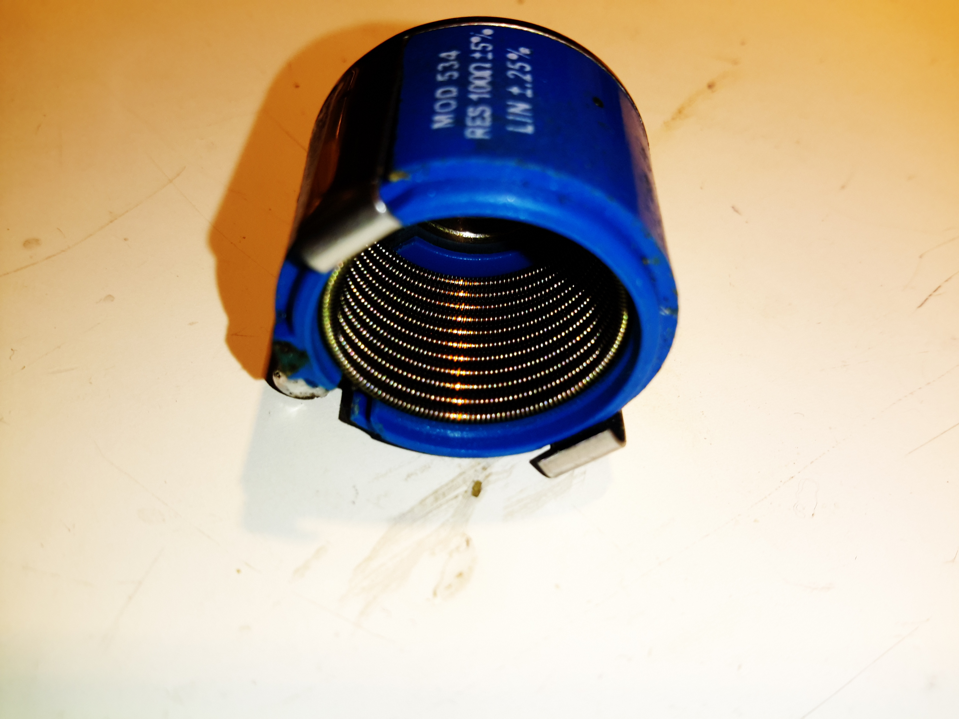
Resistance Winding
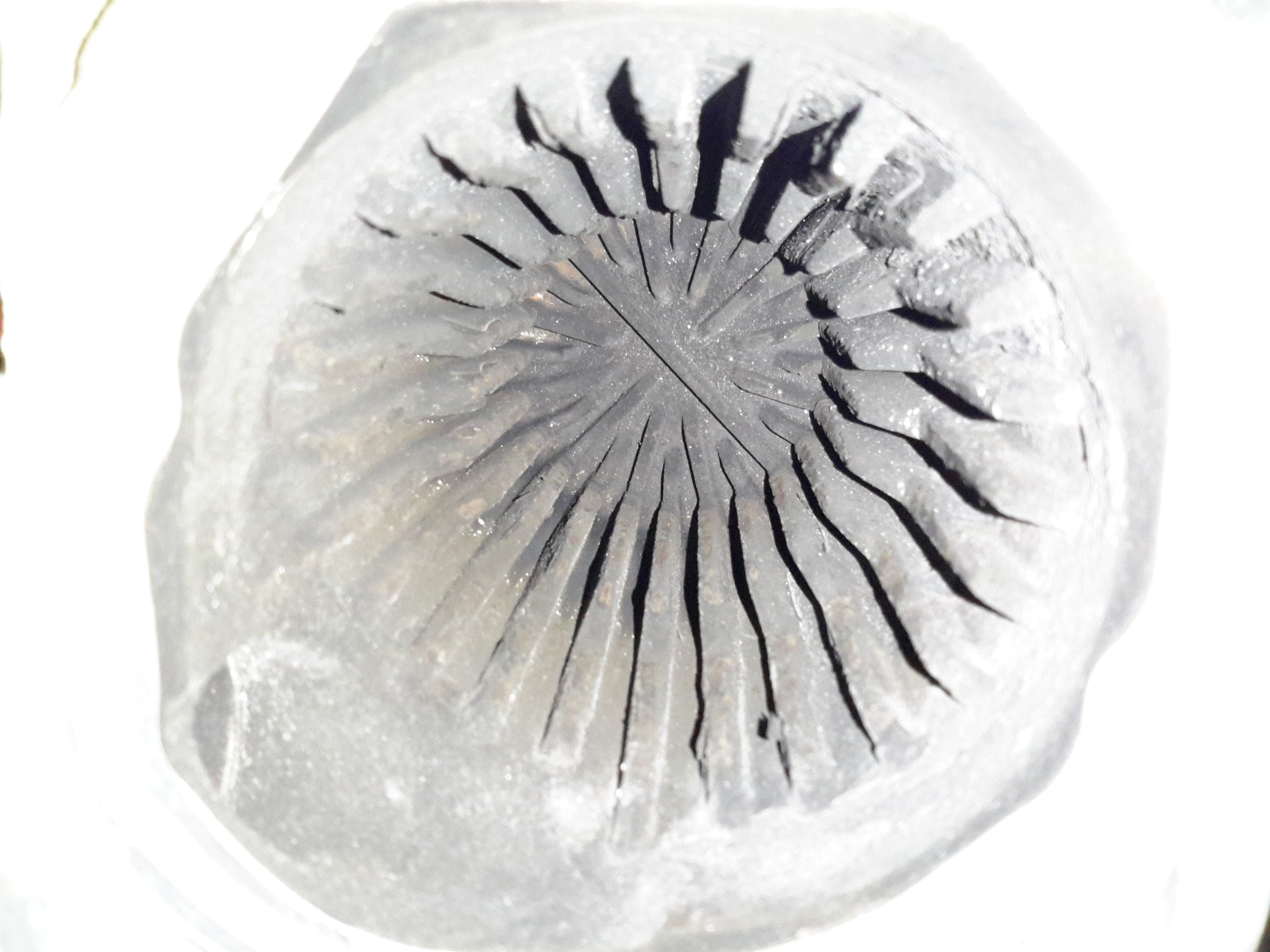
With the centre shaft & it’s wiper contact removed from the shell, the helix of resistance wire can be seen inside. Oddly, the former the resistance wire is wound around appears to be metal, possibly copper, but to keep the entire thing from shorting itself out this must be coated in insulation.
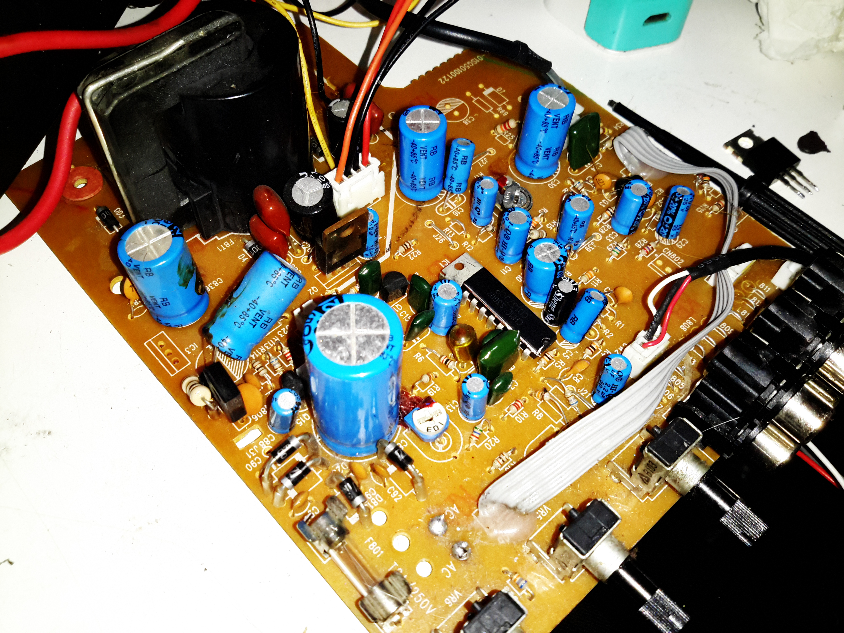
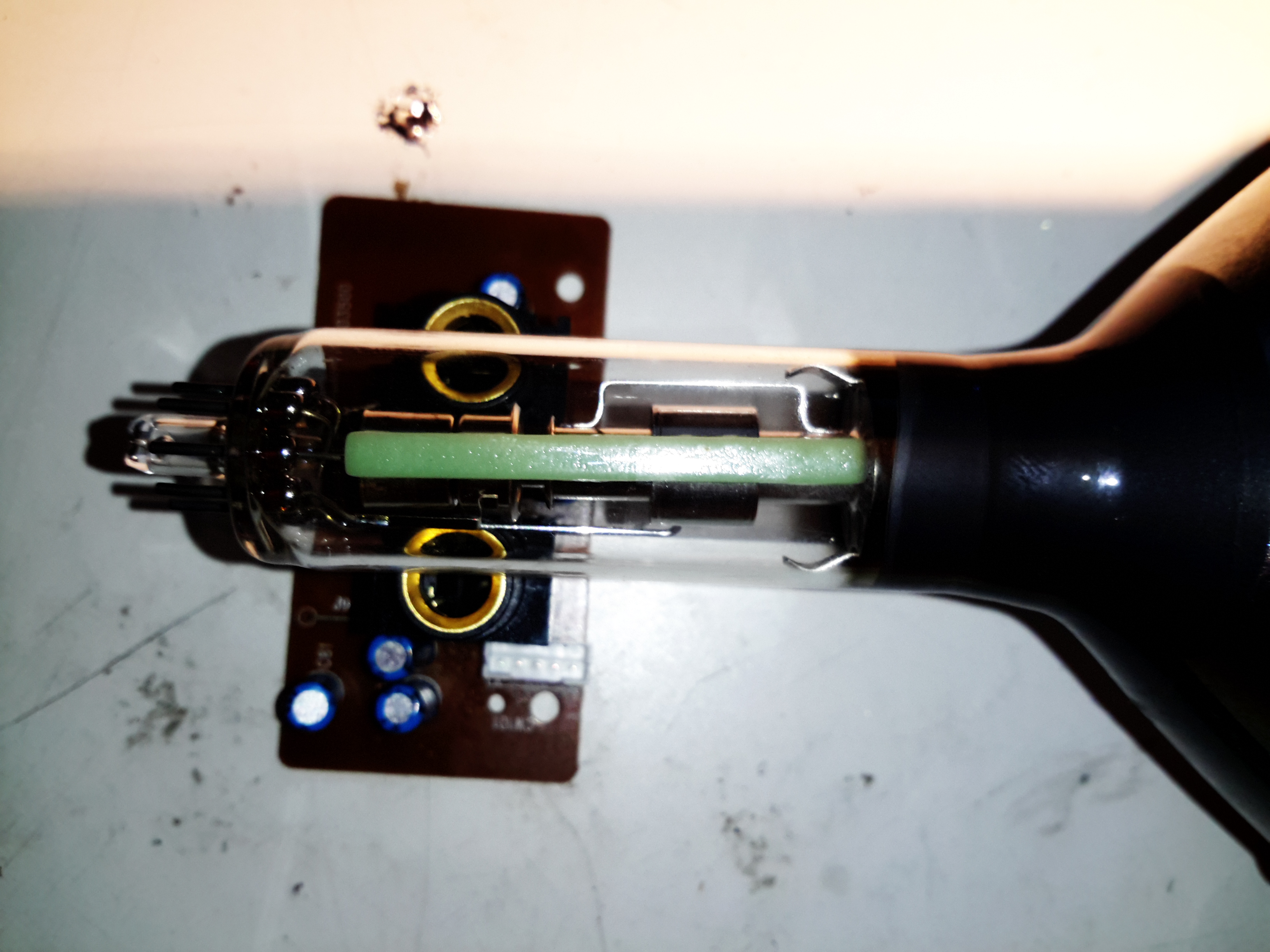
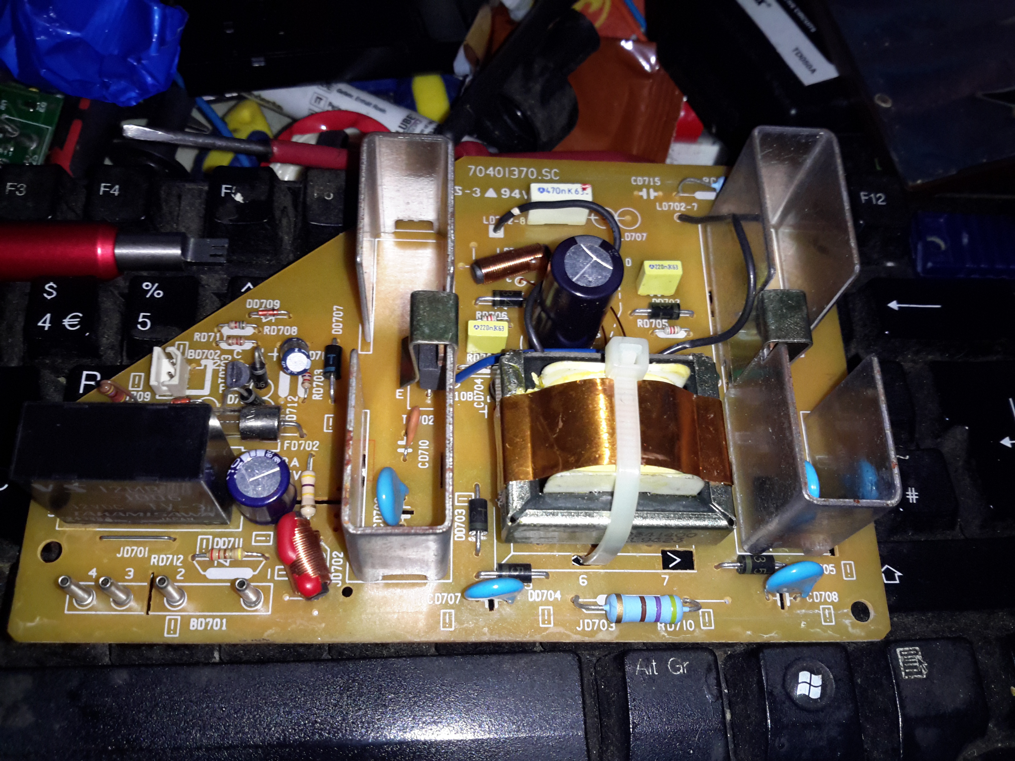
Here’s the CRT circuitry from a tossed STVG-502 Karaoke Machine, which got a good soaking in Manchester’s brilliantly wet weather before I managed to get hold of it:
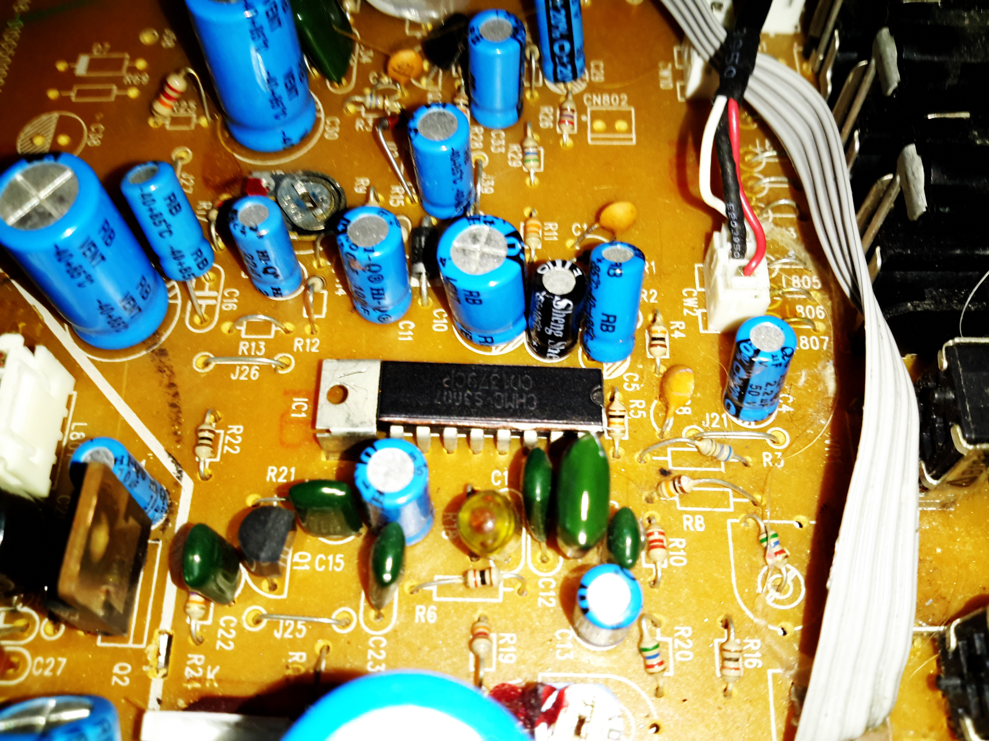
Main PCB
I didn’t do a full teardown of this unit, since it was soaking wet & smelled rather badly of sour milk, so instead I quickly gutted it for the useful parts. These machines are a combination of a CD+G player, CRT composite monitor for displaying the CD+G lyrics & a small audio amplifier & 3W speaker. Power is provided from the mains via a transformer, with both 12 & 24v windings. One half of the board has the audio amplifier sections, the other the CRT drive, running from the 12v & 24v supplies respectively. I chopped off the audio section, as that wasn’t needed.
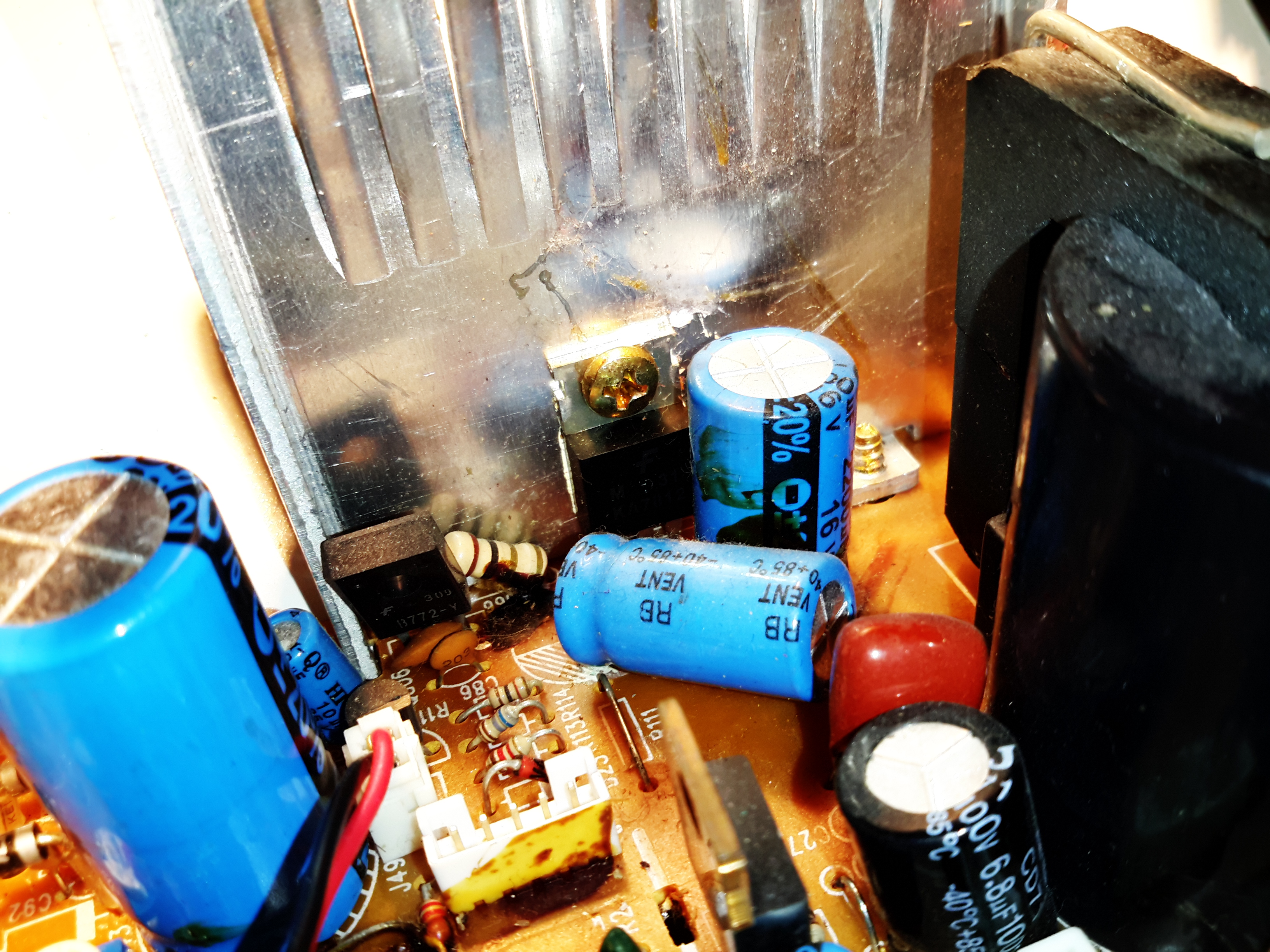
Linear Regulator
On this huge heatsink is what I originally thought was the horizontal drive transistor is actually a 12v linear regulator – the board gets fed 16v AC. This is then run through a rectifier which will produce an approx 22v rail, and after the smaller transistor on the left used for power switching. The 22v then gets dropped through a 1/2W 1Ω resistor, then the linear regulator drops it down to 12v for the rest of the circuit – dissipating a goodly amount of power in the process.
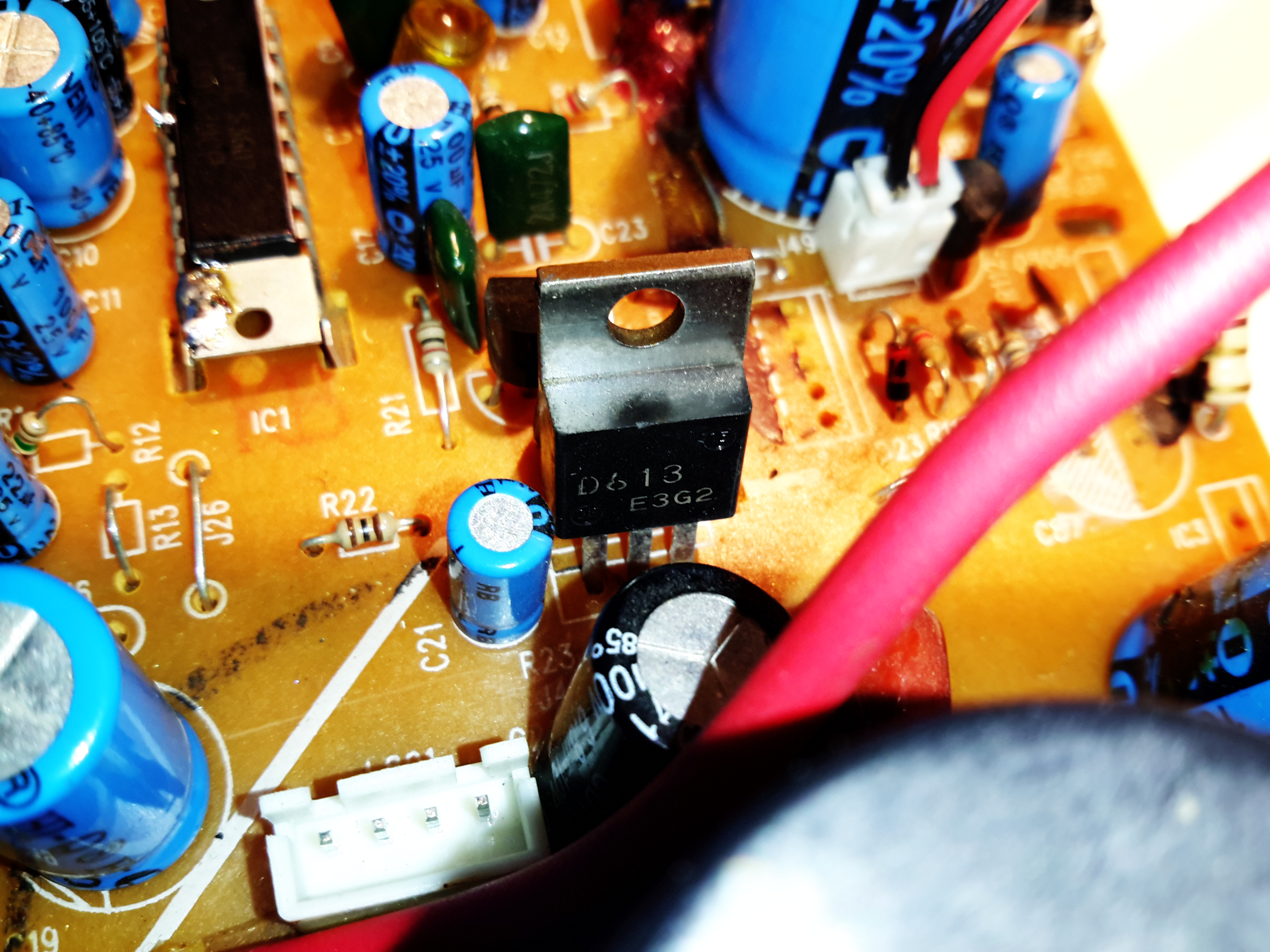
Horizontal Output Transistor
This is in fact the horizontal drive transistor, a 2SD613, which according to the datasheet, is intended for audio amplifier output stage applications, not CRT drive. Regardless, it’s an 85v 6A NPN transistor, and does get a bit on the warm side, but was never given a heatsink from the factory.
CRT Drive IC
All the drive signals for the CRT are taken care of by this single DIP IC – a CD1379CP from Silicore. Considering the older CRT-based devices I have, with entire boards twice the size of this one dedicated to discrete components required to drive a CRT, this is definitely an advance in technology. Very few external components are being used, and no custom magnetics.
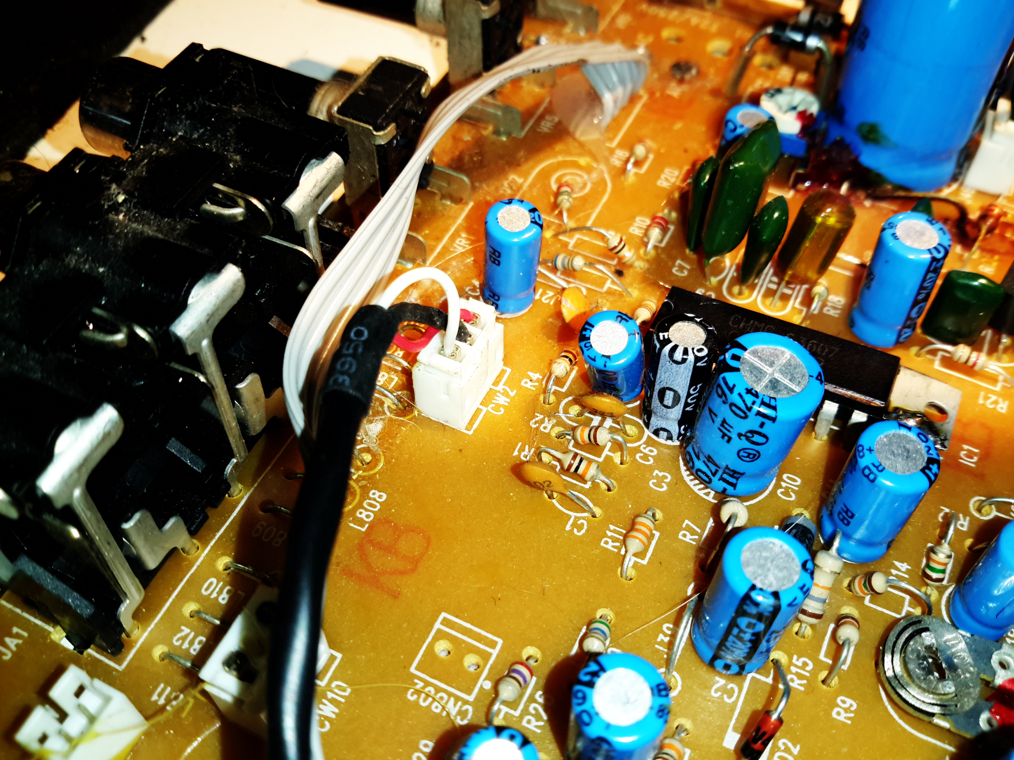
Video Input
The video signal comes in from the CD+G player module on this connector, it’s a standard composite input. The composite video is fed into an amplifier after the controller IC. This video amp is powered from a 140v rail from the flyback transformer, to give enough signal to drive the CRT cathode.
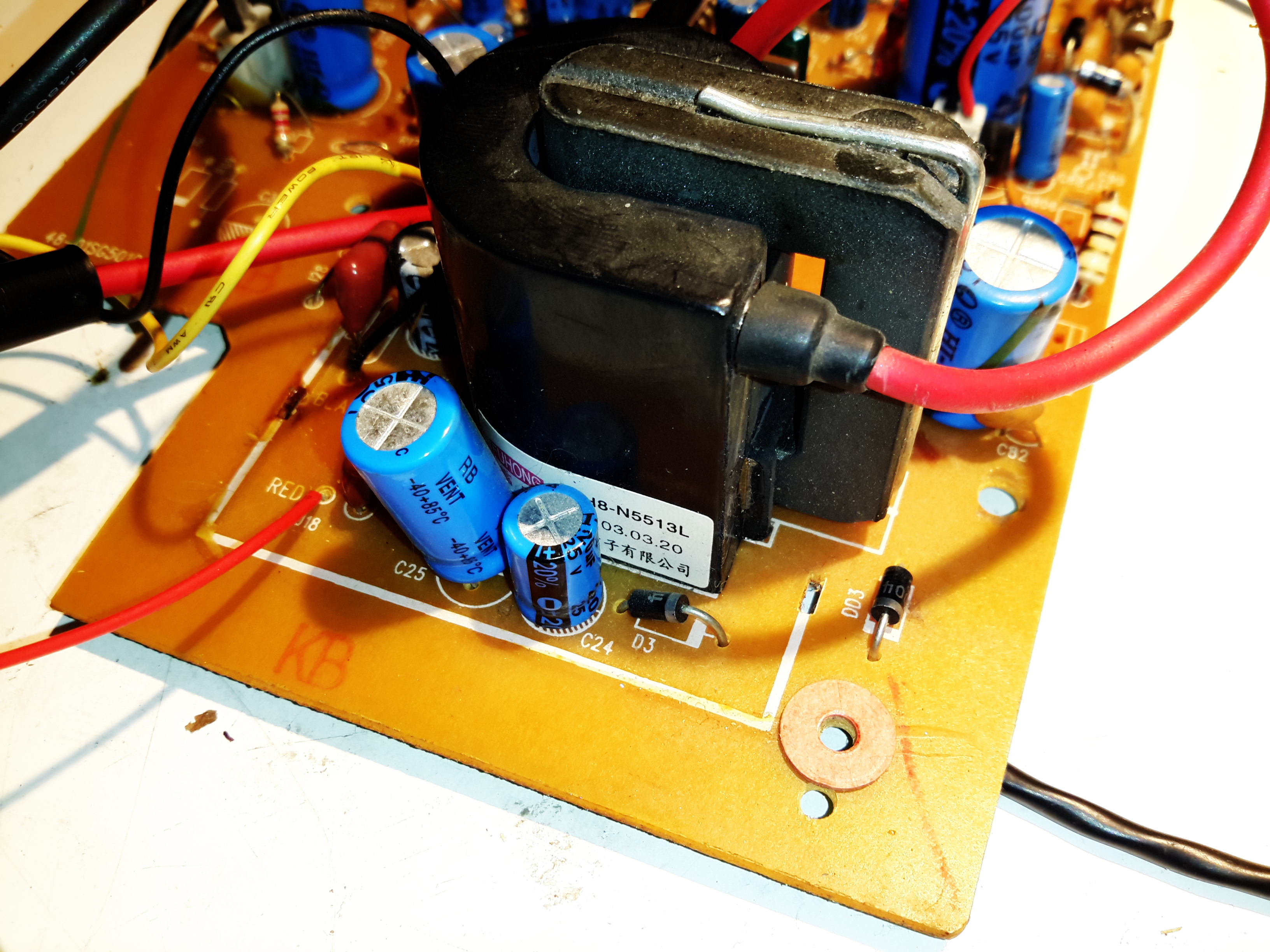
LOPT
The high voltage transformer is a BSH8-N5513L, I’ve not been able to find any data on this, but it looks like a standard off the shelf transformer from the listings on the Chinese supplier sites. There are very few support components around here, just a couple of diodes to rectify the high voltage focus supply, and no linearity coil. Weirdly, the 1st accelerating anode of the tube is grounded in this circuit. Very few adjustments are provided, most are set with fixed resistors to keep the cost low.
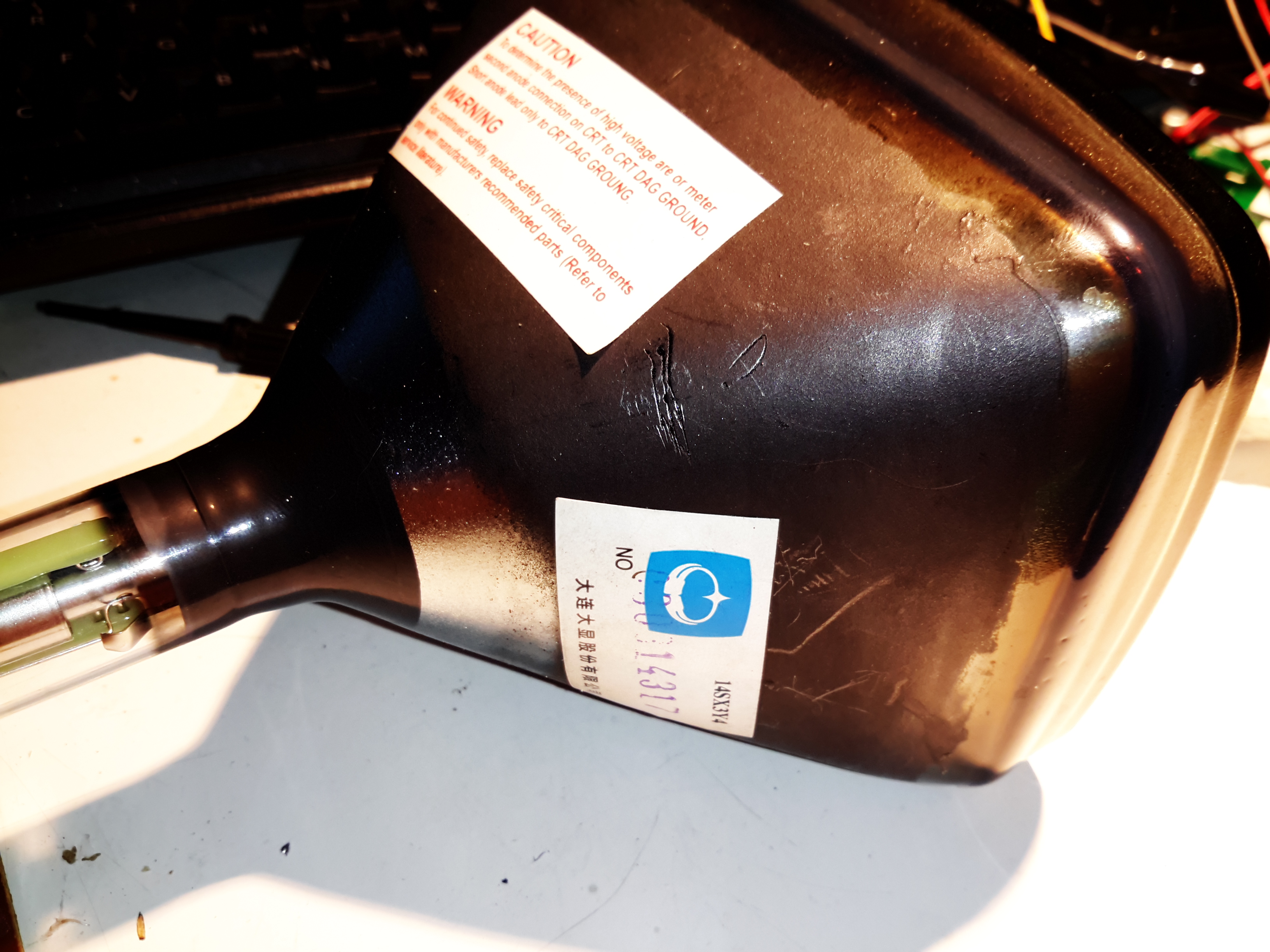
The CRT
14SX3Y4 CRT
Here’s the CRT, it’s a 5″ monochrome model. I’ve not been able to find much data on this either.
Bent Electron Gun
Seems the gents in the Shenzhen factory were having a bit of an off day when this one was made – the electron gun assembly is actually tilted in the neck of the tube – as a result the spot formed with no deflection is far from the centre of the screen. This tube does still produce a pretty good picture though, this manufacturing error is easily corrected for with the positioning magnets on the deflection yoke.
Final Mods
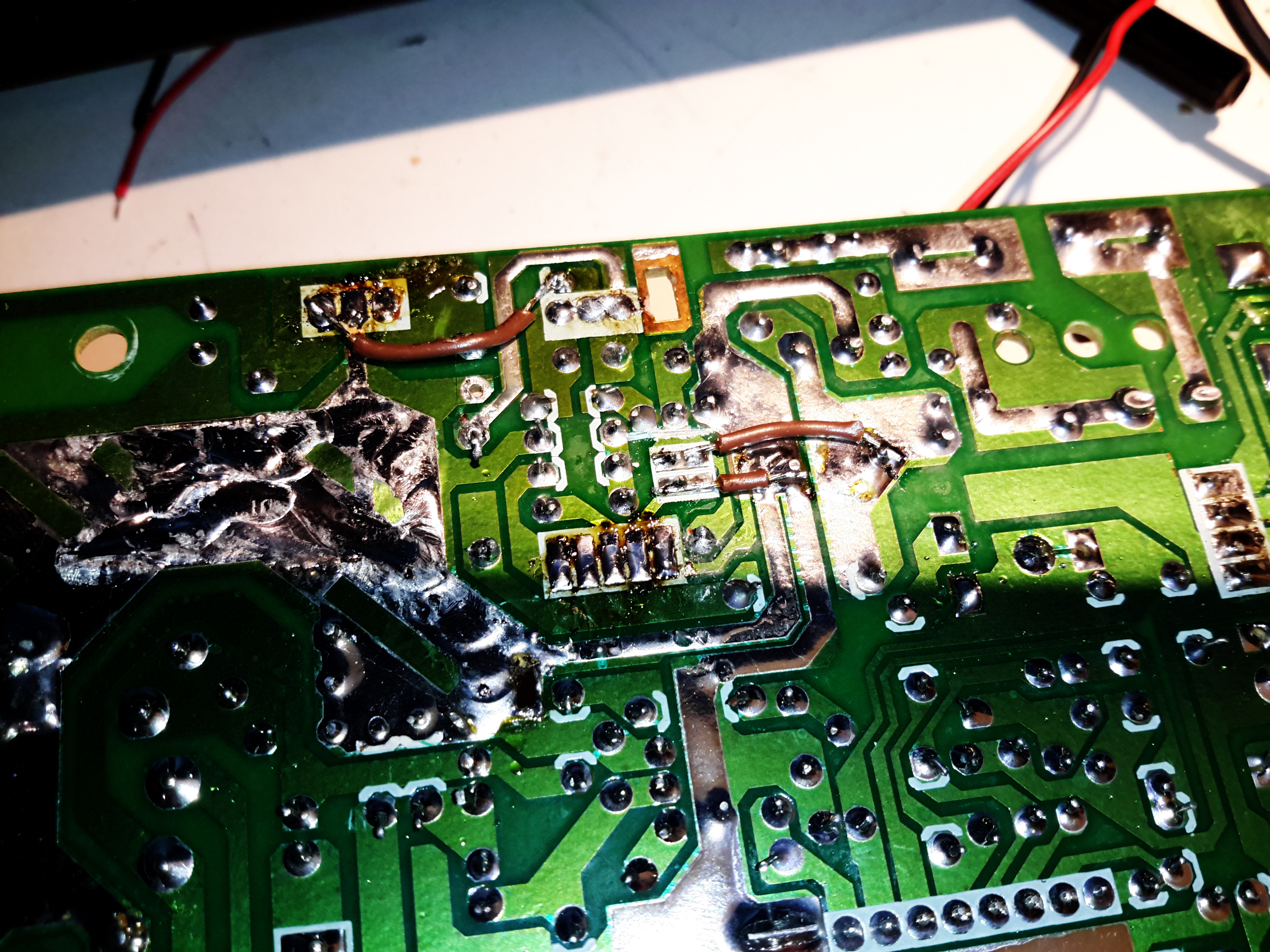
PCB Mods
I’ve installed a couple of mod wires on the bottom of the PCB to get this to work outside the original application, without the room heater of a linear regulator in circuit this will run fine from a 12v supply. The PCB quality is a bit naff – even quick heating with a soldering iron makes tracks fall off the laminated paper board.
Image Display
Image quality is surprisingly good for the cheapest CRT-based monitor I’ve ever seen, I figured a Fallout reference was required here; anyone for a proper CRT-based PipBoy? 😉 Shame the phosphor isn’t green.
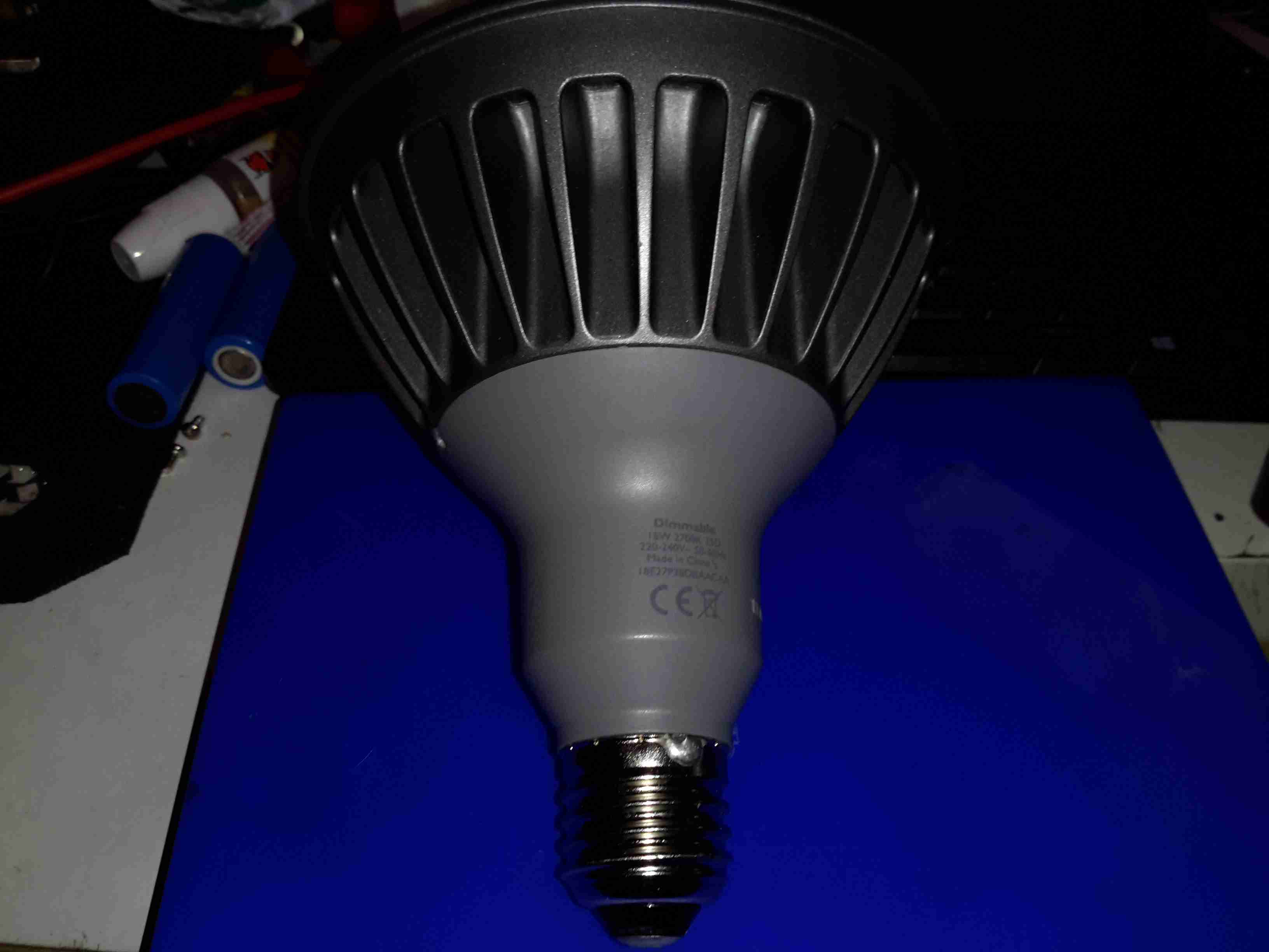
These large LED Philips PAR38 lamps were recently on clearance sale in my local T.N. Robinsons electrical contractors for about £3, so I decided to grab one in the hopes I might be able to hack it into a low-voltage LED lamp. These are full-size PAR38 format, with most of the bulk being the large aluminium heatsink on the front. The back section with the power supply module is secured with silicone, so some unreasonable force was required to liberate the two pieces.
Specification
These lamps are rated at 18W in operation, and are surprisingly bright for this power level.
Lens
The front has the moulded multi-lens over the LEDs, to spread the light a bit further than the bare dies.
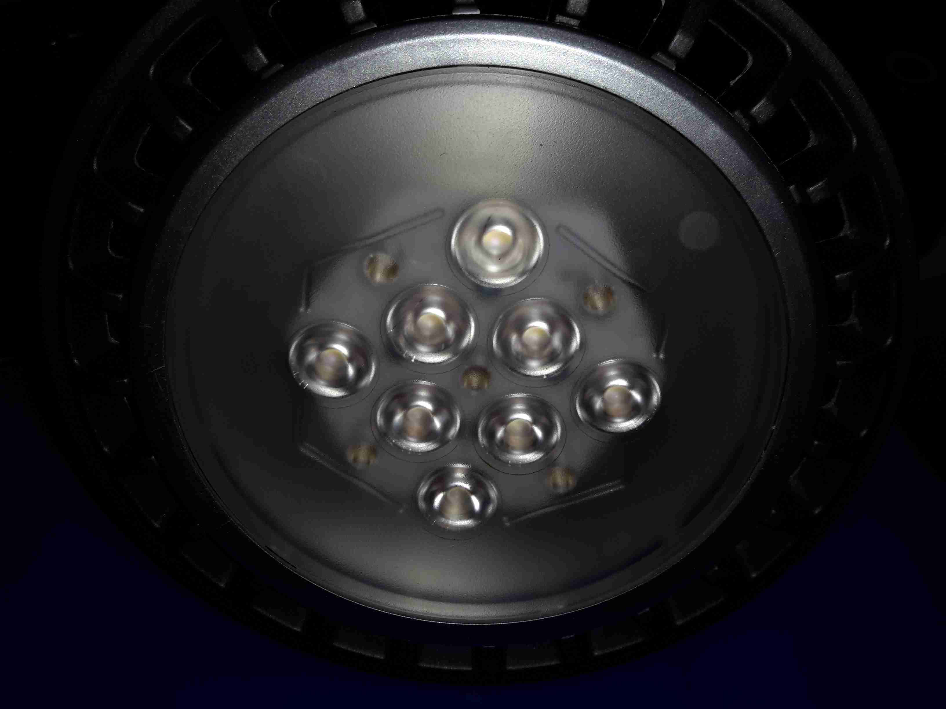
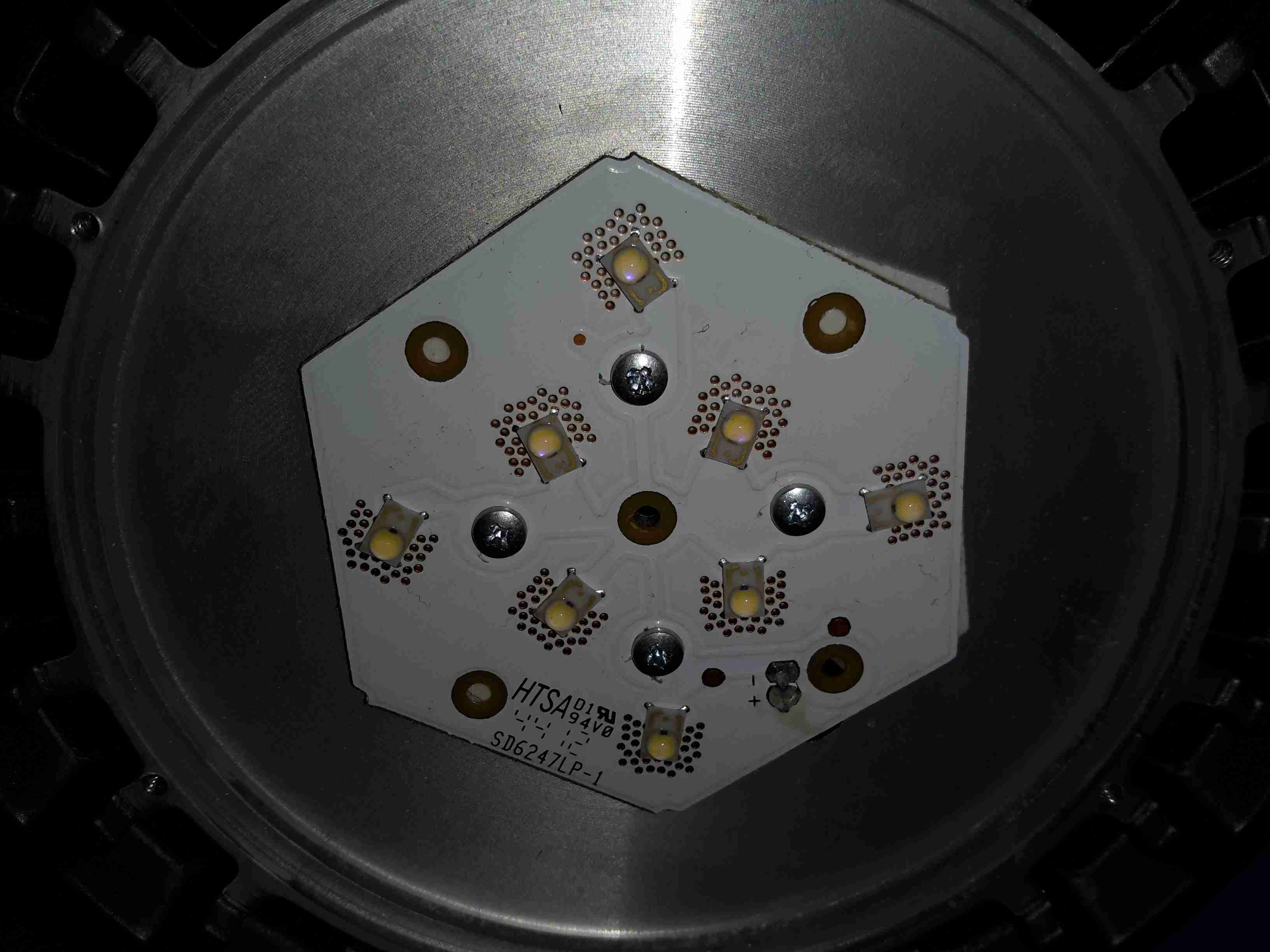
LED Array
The LED array is two series strings of 4 LEDs, for ~24v forward voltage. Unusual for a high power LED array, this PCB isn’t aluminium cored, but 0.8mm FR4. Heat is transferred to the copper plane on the backside by the dozens of vias around the Luxeon Rebel LEDs. There is a thermal pad under the PCB for improved heat transfer to the machined surface of the heatsink.
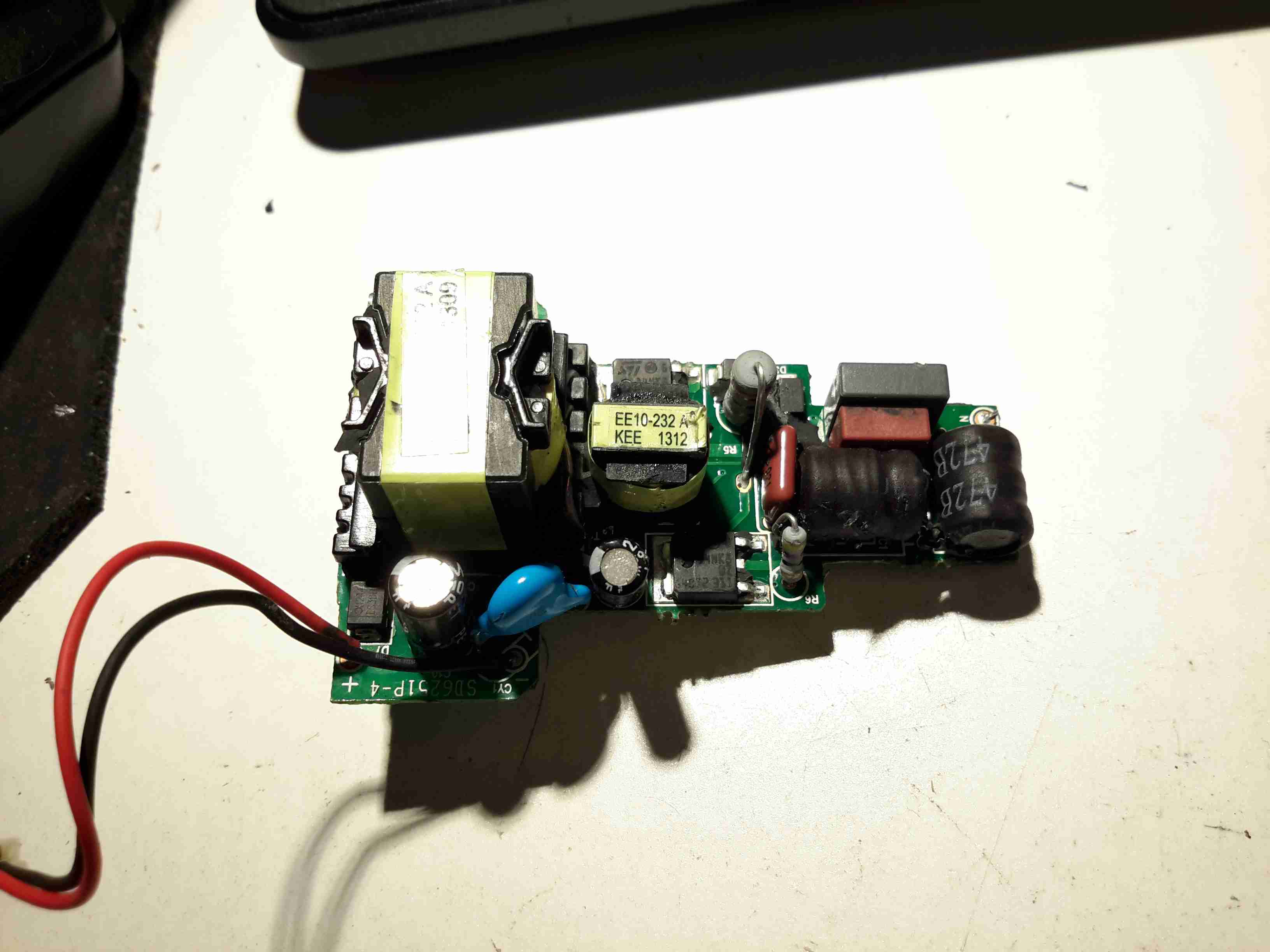
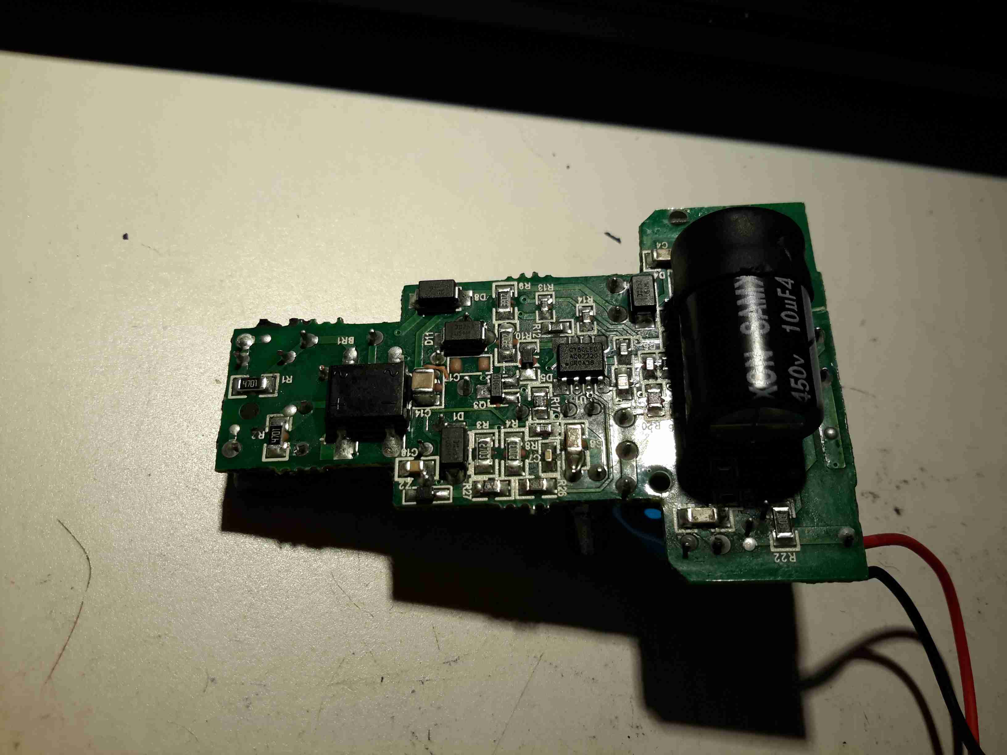
Control PCB Top
The power supply & control PCB is pretty well made, it’s an isolated converter, so no nasty mains on the LED connections.
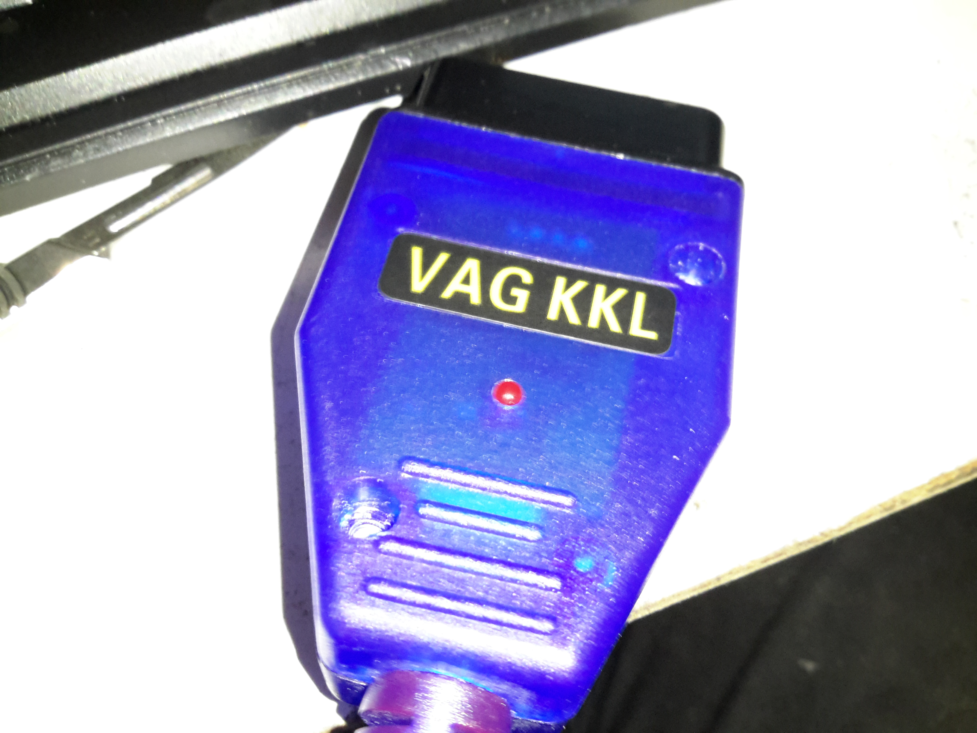
This is a little bit of kit I got to talk to the Webasto TT-V I salvaged from a scrap Jaguar S-Type, and converts USB-RS232 to the standard car diagnostic ODB connector. (These are a much cheaper option at £4 than the official Webasto diagnostic adaptor & loom which is over £90.
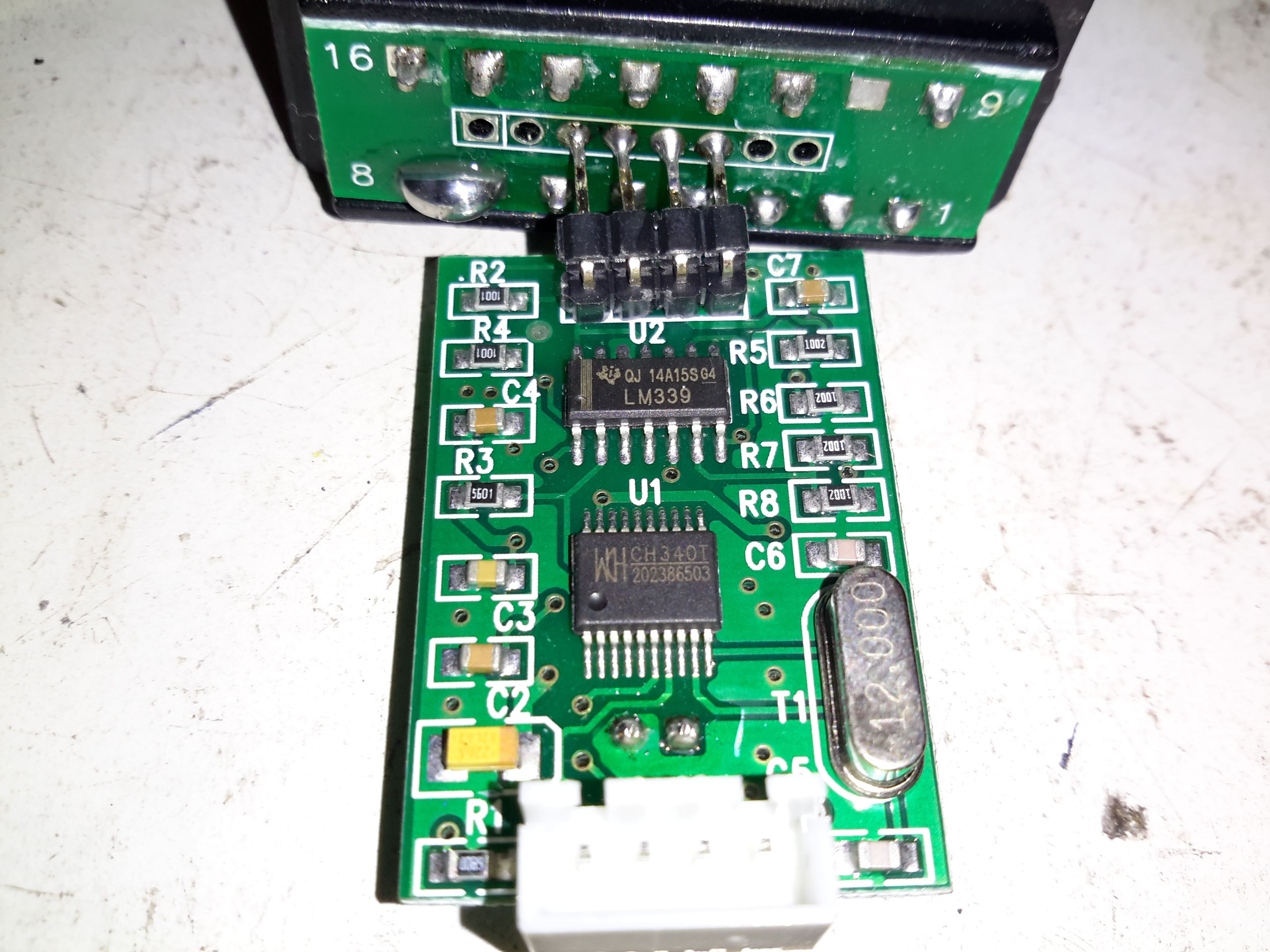
PCB Top
There’s really not much to this adaptor, the only signals that are routed to the ODB connector seem to be the +12v on pin 16, K-Line on Pin 7 & L-Line on pin 15. The main IC here is a CH340 USB-Serial interface, with some glue logic in the form of an LM339 quad comparator.
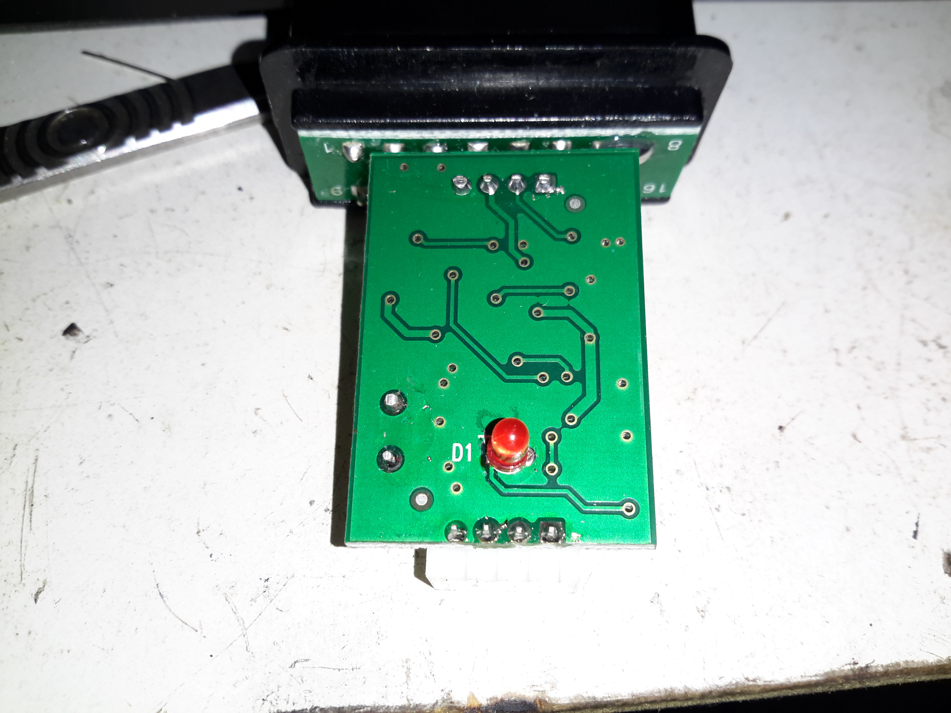
PCB Reverse
The reverse side of the PCB only has the power indicator LED.
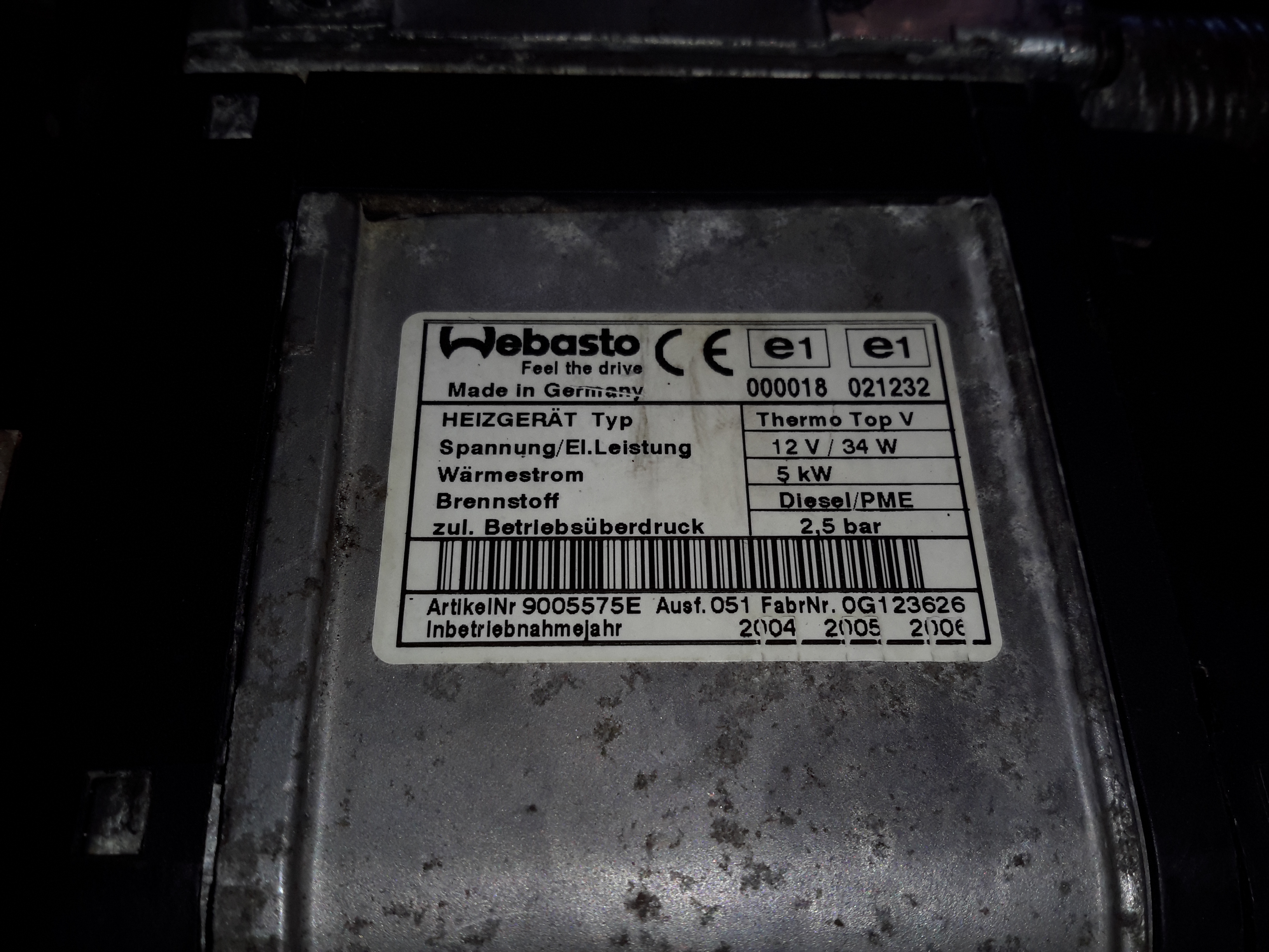
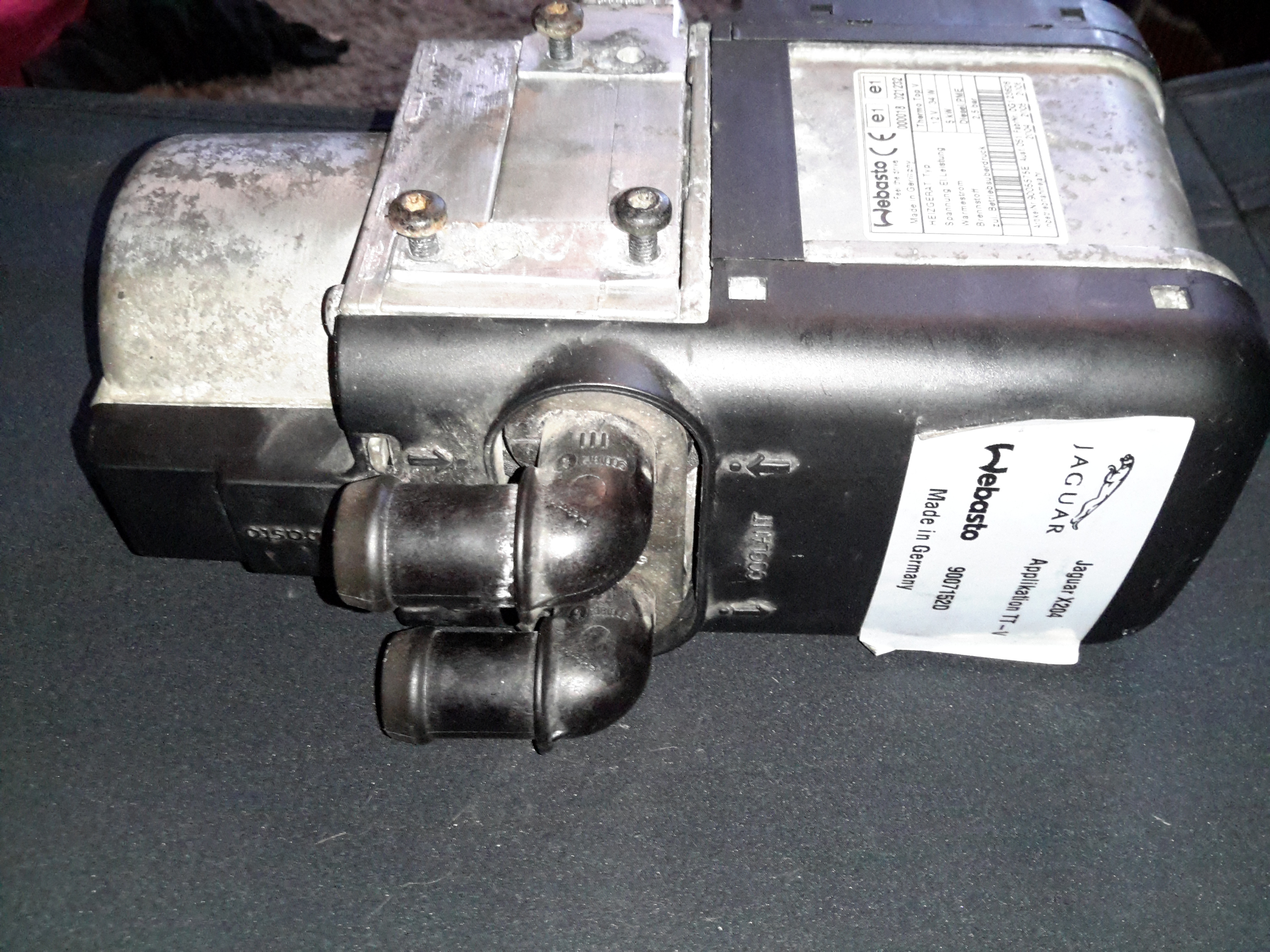
Here’s another Diesel-fired heater related project – these Webasto heaters are fitted to Jaguar S-Type cars as auxiliary heaters, since (according to the Jag manual), the modern fuel-efficient diesels produce so little waste heat that extra help is required to run the car’s climate control system. (Although this seems to nullify any fuel efficiency boost, as the fuel saved by not producing so much waste heat in the engine itself is burned in an aux heater to provide heat anyway). The unfortunate part is these units don’t respond to applying +12v to Pin 1 of the ECU to get them to start – they are programmed to respond to CAN Bus & K-Line Bus only, so they require a bit more effort to get going. They also don’t have a built-in water circulation pump unlike the Webasto Thermo Top C heaters – they expect the water flow to be taken care of by the engine’s coolant pump.
Webasto LabelWater Side
The water ports are on the side of this heater instead of the end, the heat exhanger is on the left. These hearers are fitted to the car under the left front wing, behind a splash guard. Pretty easy to get to but they get exposed to all the road dirt, water & salt so corrosion is a little problem. The fuel dosing pump is in a much more difficult spot to get at – it’s under the car next to the fuel tank on the right hand side. Access to the underside with stands is required to get at this.
ECU Side
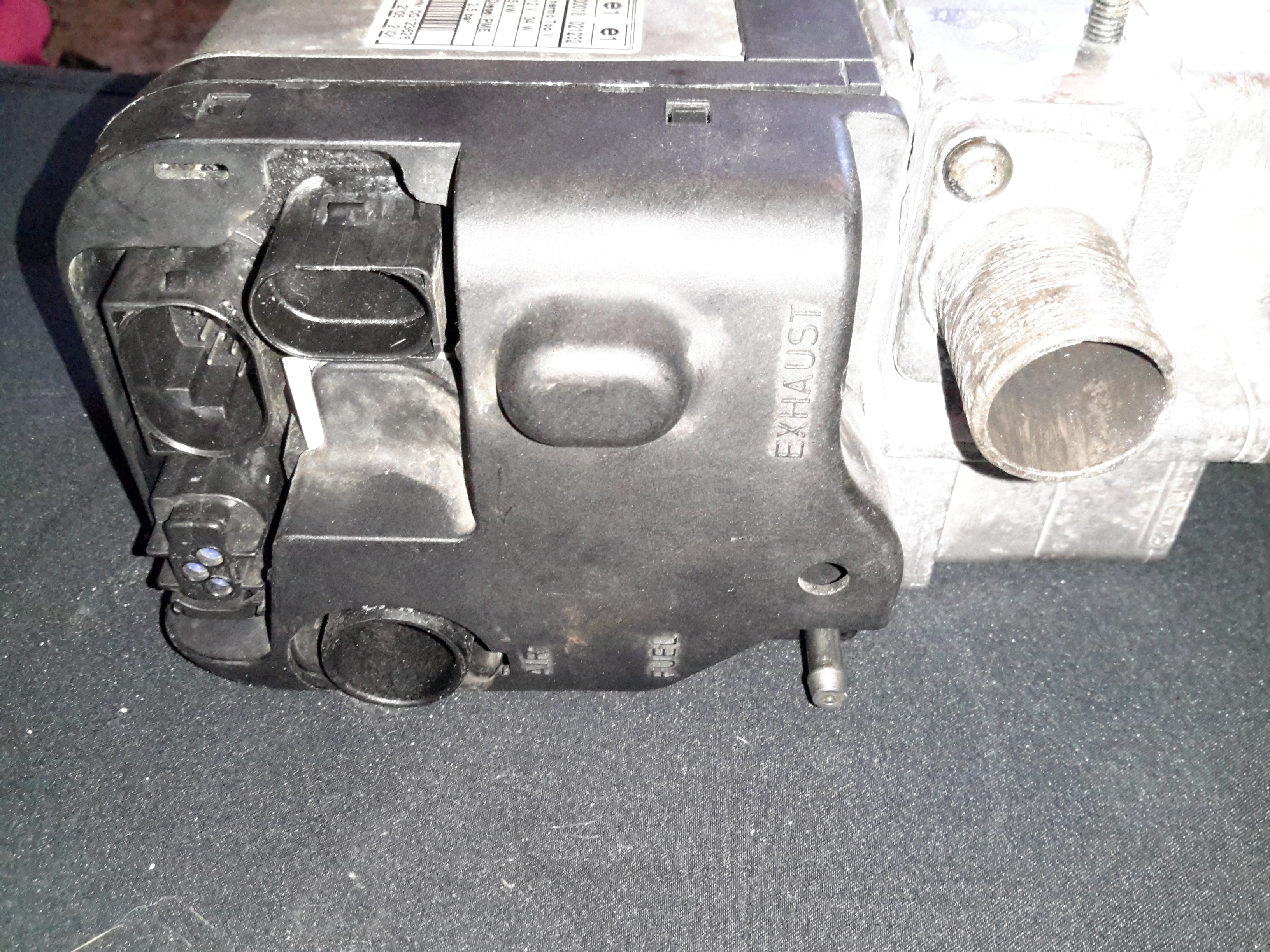
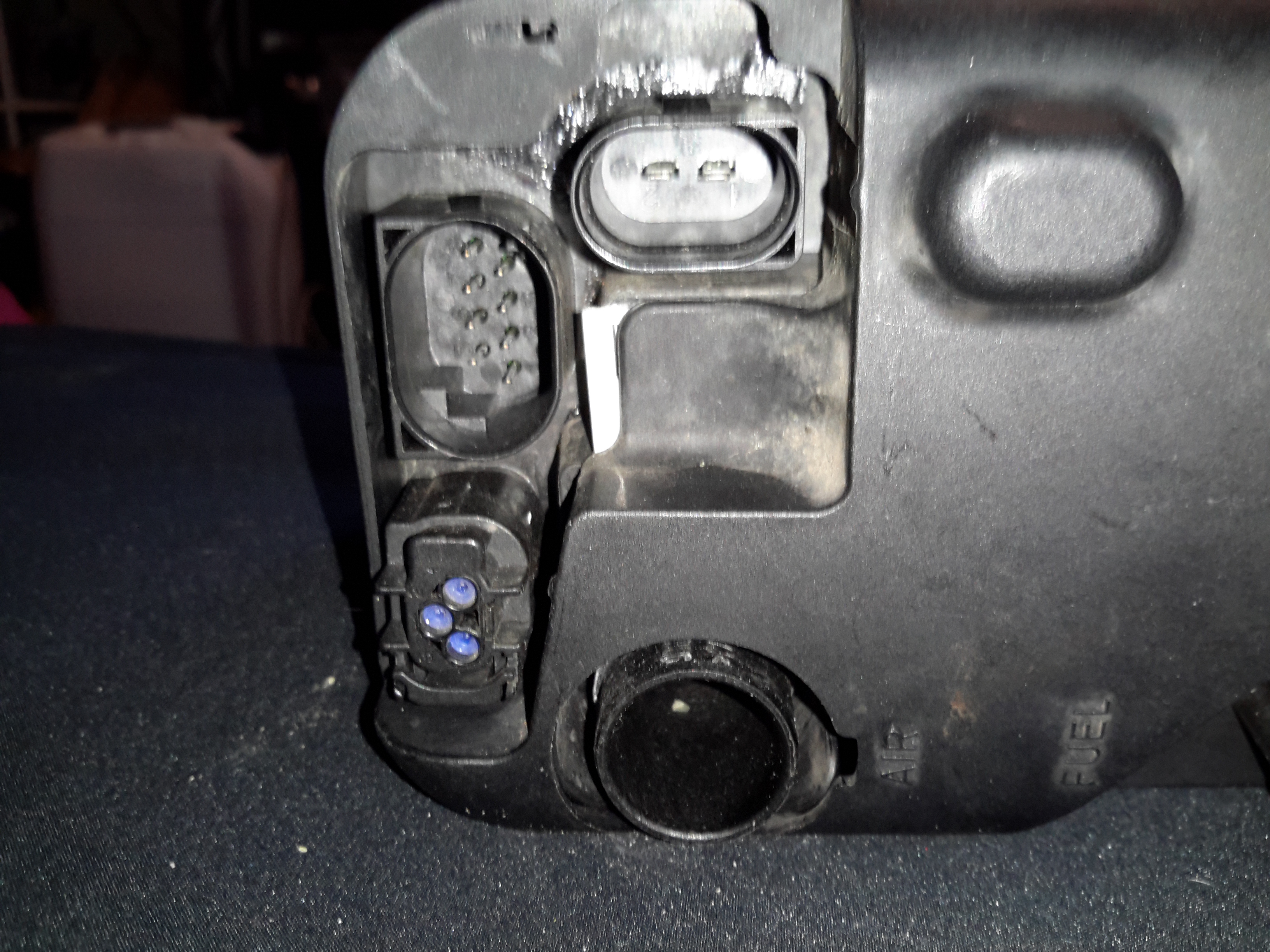
The ECU side has all the other connections – Combustion air, exhaust, fuel, power & control.
External Connectors
Only two of the external connectors are used on these heaters, the large two pin one is for main power – heavy cable required here as the current draw can climb to ~30A on startup while the glow plug fires. The 8-pin connector on the left is the control connector, where the CAN / K-Line / W-Bus buses live. The fuel dosing pump is also supplied from a pin on this connector. The small 3-pin under that is a blank for a circulation pump where fitted. Pinouts are here:
Pin
Signal
1
Battery Positive
2
Battery Negative
Pin Number
Signal
Notes
1
Telestart / Heater Enable
Would usually start the heater with a simple +12v ON signal, but is disabled in these heaters.
2
W-Bus / K-Line
Diagnostic Serial Bus Or Webasto Type 1533 Programmer / Clock
3
External Temp Sensor
4
CAN-
CAN Bus Low
5
Fuel Dosing Pump
Fuel Pump output. Connect pump to this pin & ground. Polarity unimportant.
6
Solenoid Valve
Fuel cutoff solenoid optionally fitted here.
7
CAN+
CAN Bus High
8
Cabin Heater Fan Control
This output switches on when heater reaches +50°C to control car heater blower
Pin
Signal
Notes
1
?
?
2
Circulation Pump +
3
Circulation Pump -
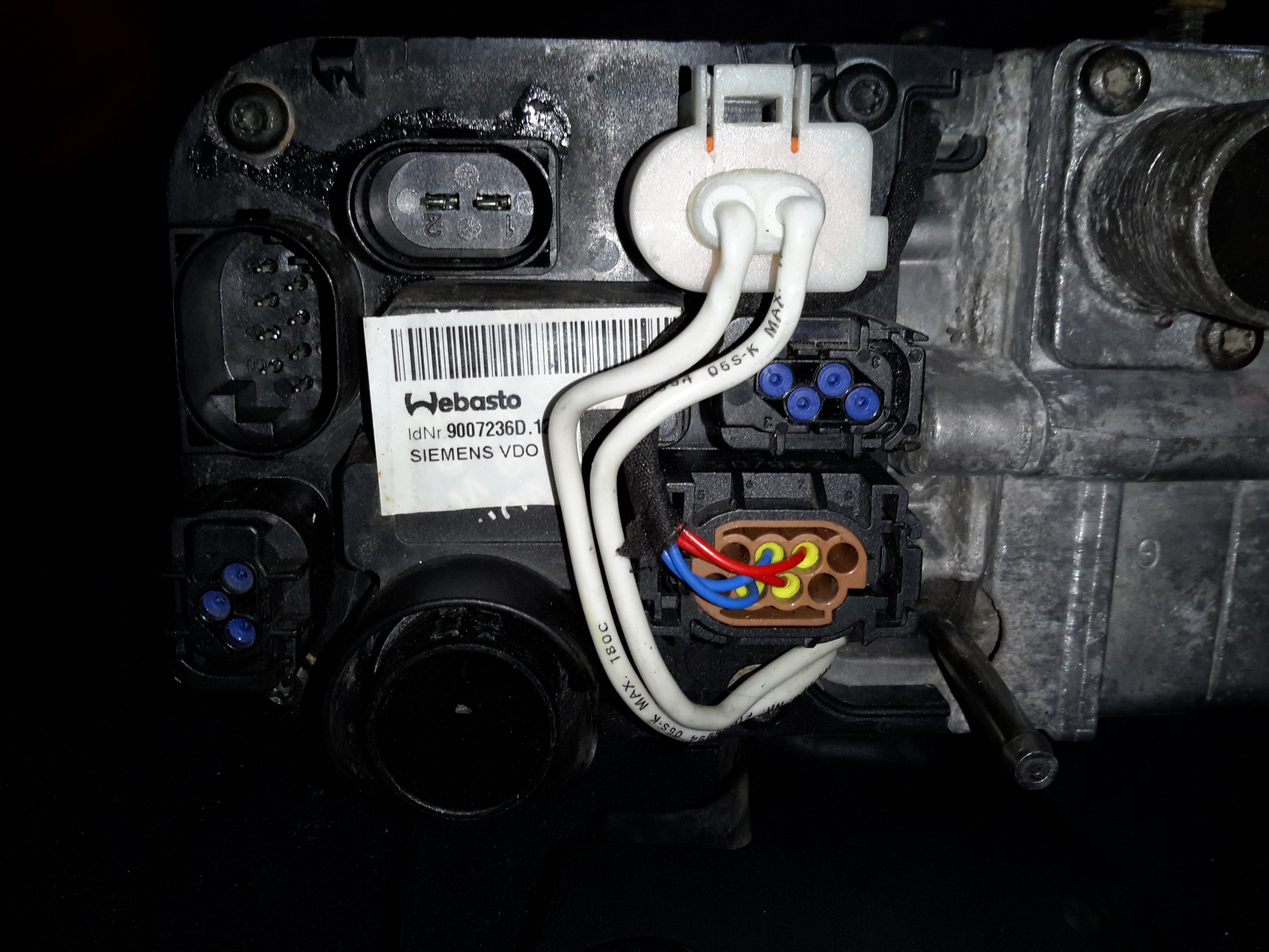
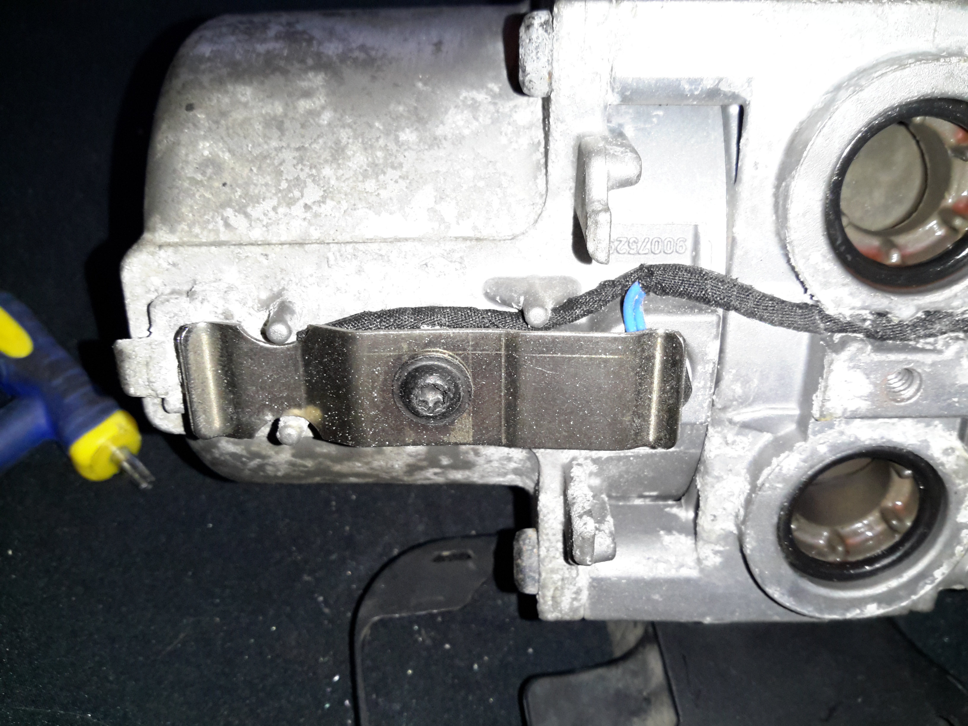
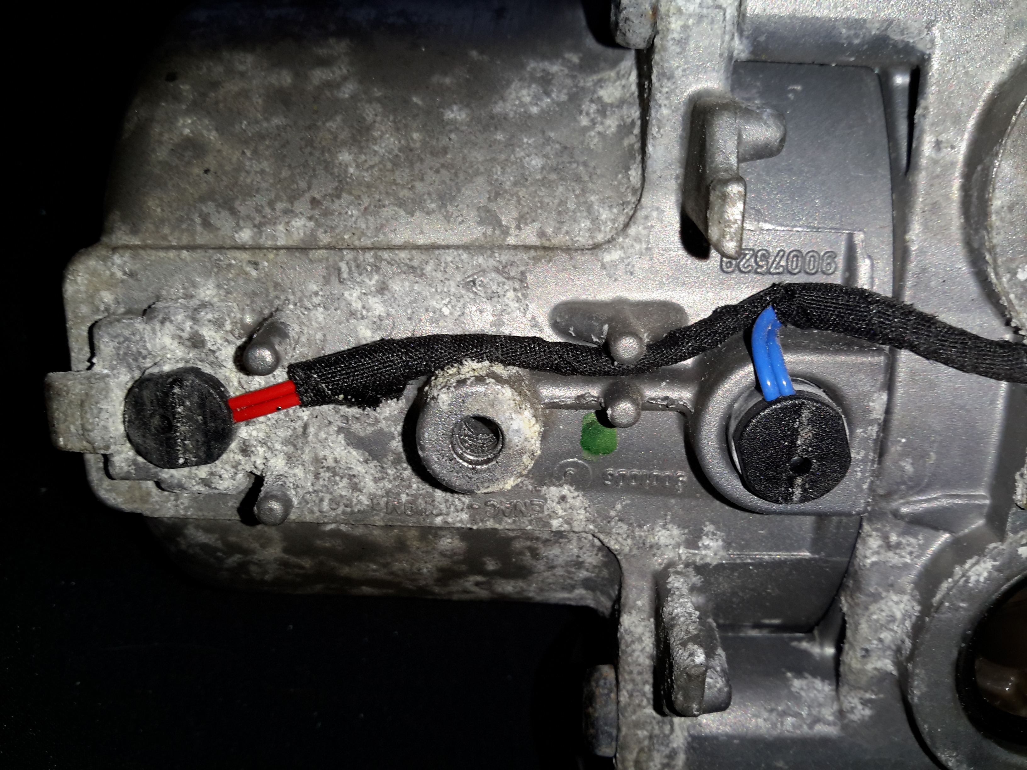
ECU Cover Removed
Removing the clipped-on plastic cover reveals the other ECU connectors. The large white one feeds the glow plug, & the large multi-pin below brings in the temp & overheat sensor signals.
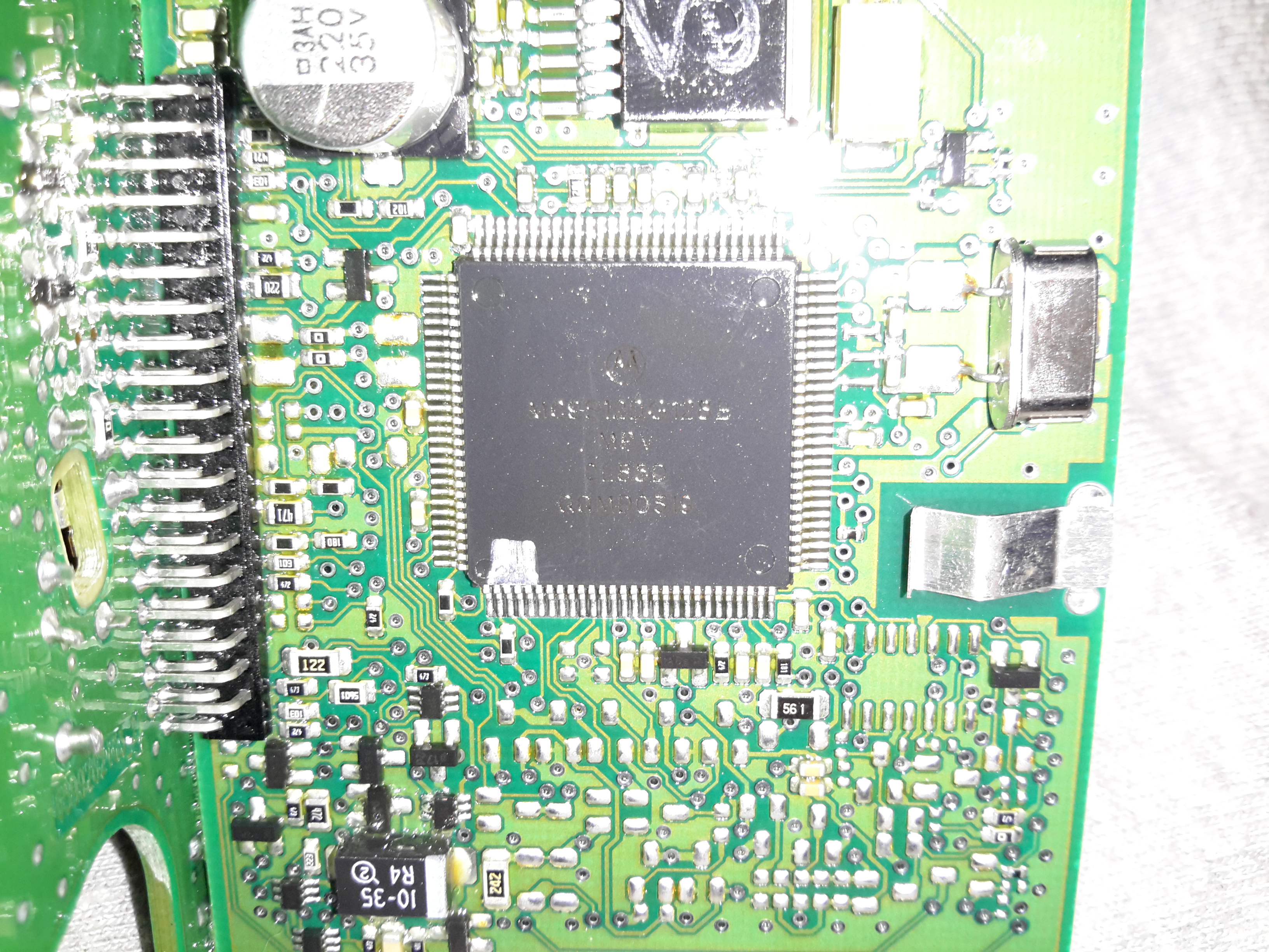
MC9S12DT128B Microcontroller
The heart of the ECU is a massive microcontroller, a Freescale MC9S12DT128B, attached to a daughterboard hooked into the ECU power board.
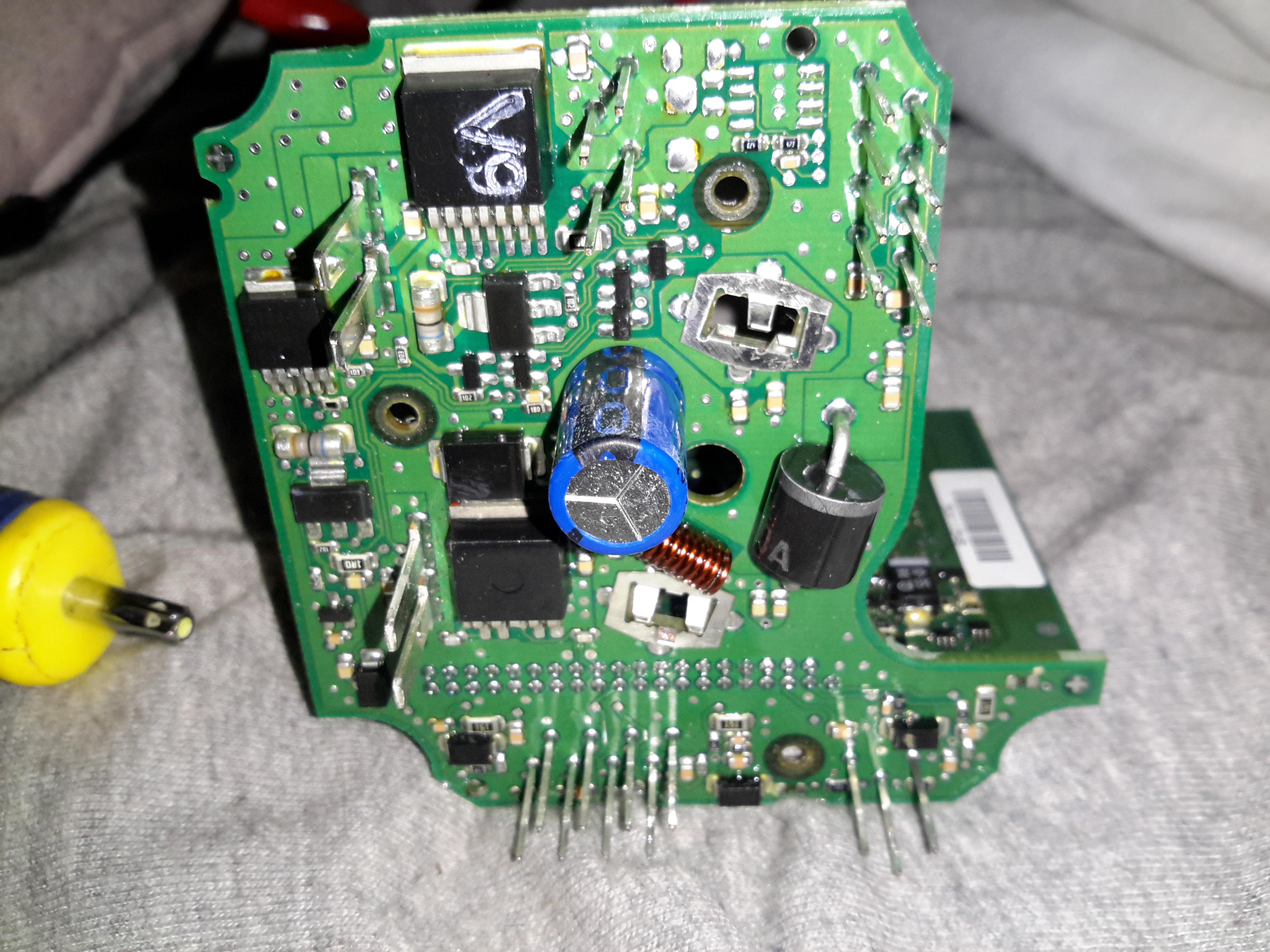
Power Section
The high power section is on the board just under the connectors, here all the large semiconductors live for switching the fan motor, glow plug, external loads, etc.
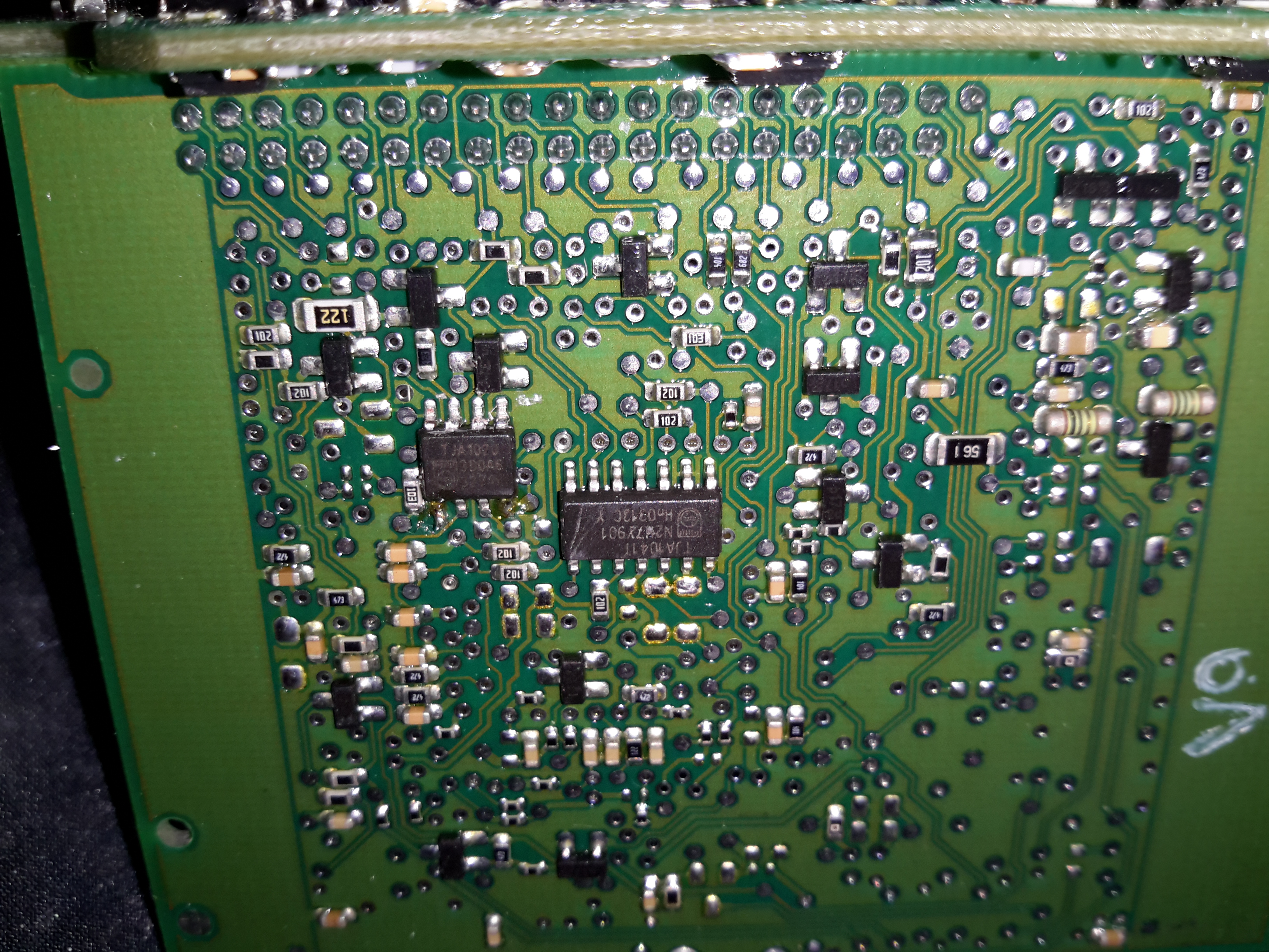
LIN & CAN Bus Transceivers
The bus transceivers are separate ICs on the control board, a TJA1041 takes care of the CAN bus. There’s also a TJA1020 LIN bus transceiver here, which is confusing since none of the Webasto documentation mentions LIN bus control.
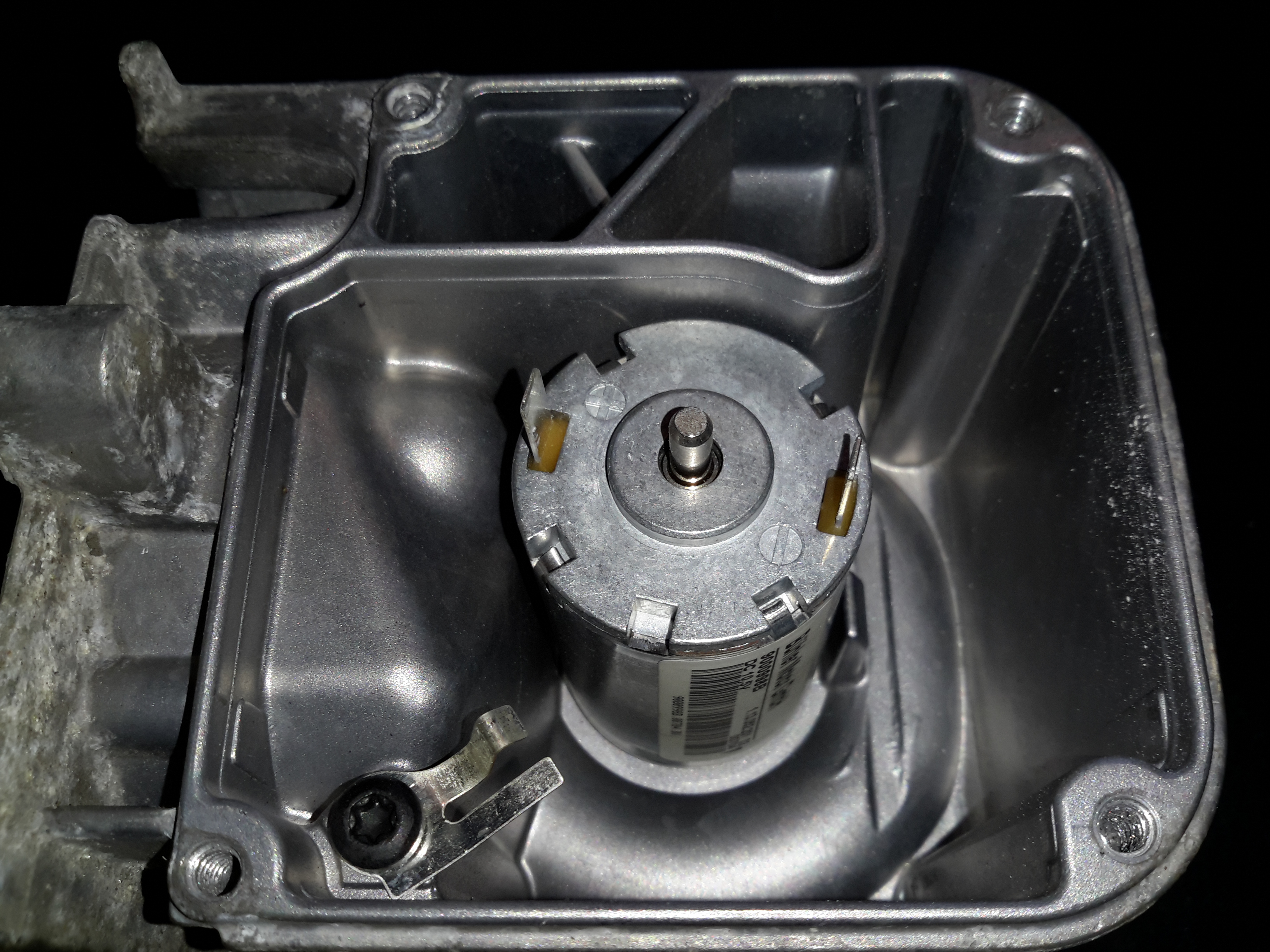
Combustion Fan Motor
The combustion fan motor is in the ECU compartment, nicely sealed away from the elements. There is no speed sensor on these blowers, unlike the Eberspacher ones.
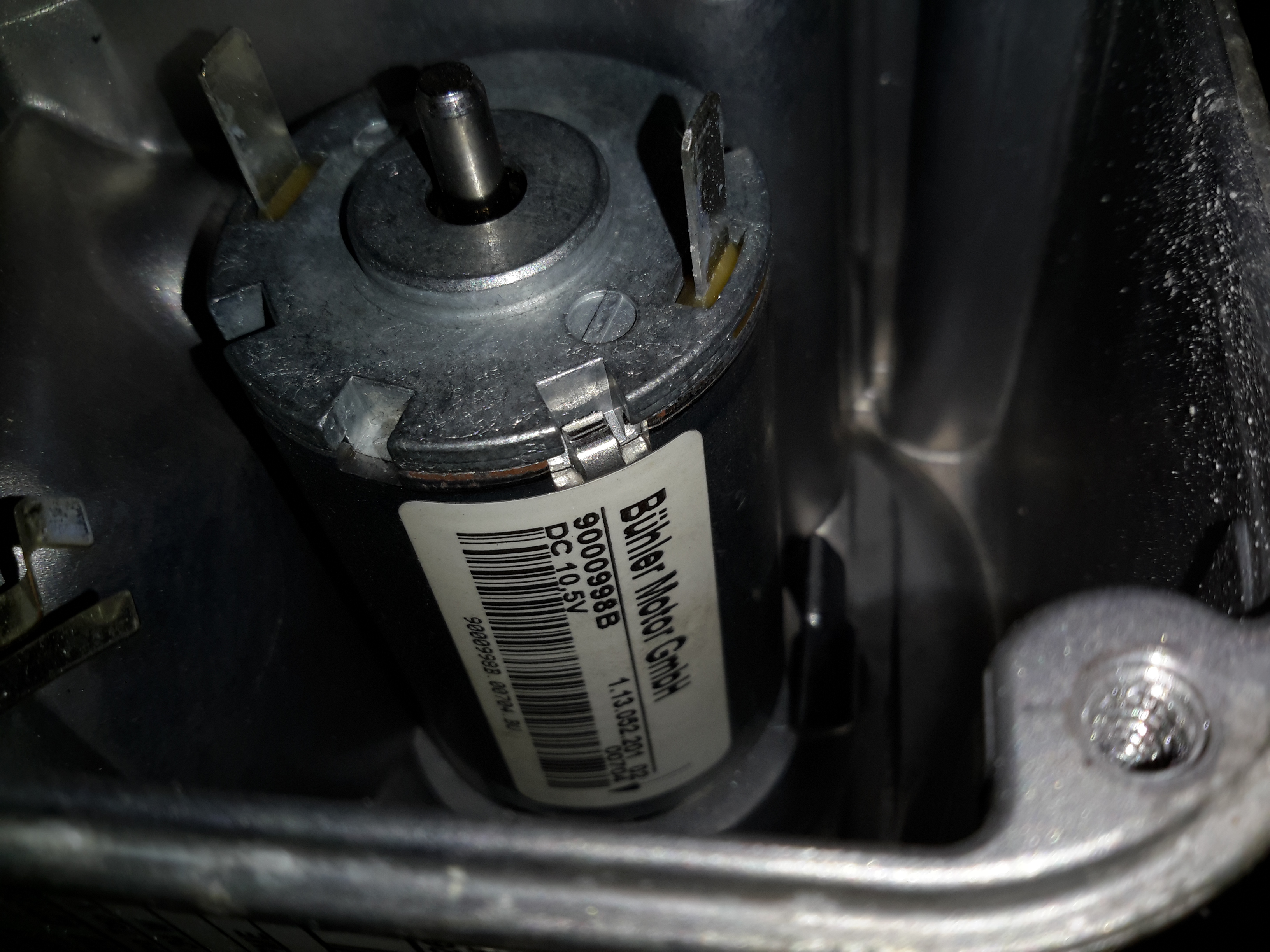
Motor Details
The motor is a Buhler, rated at 10.5v.
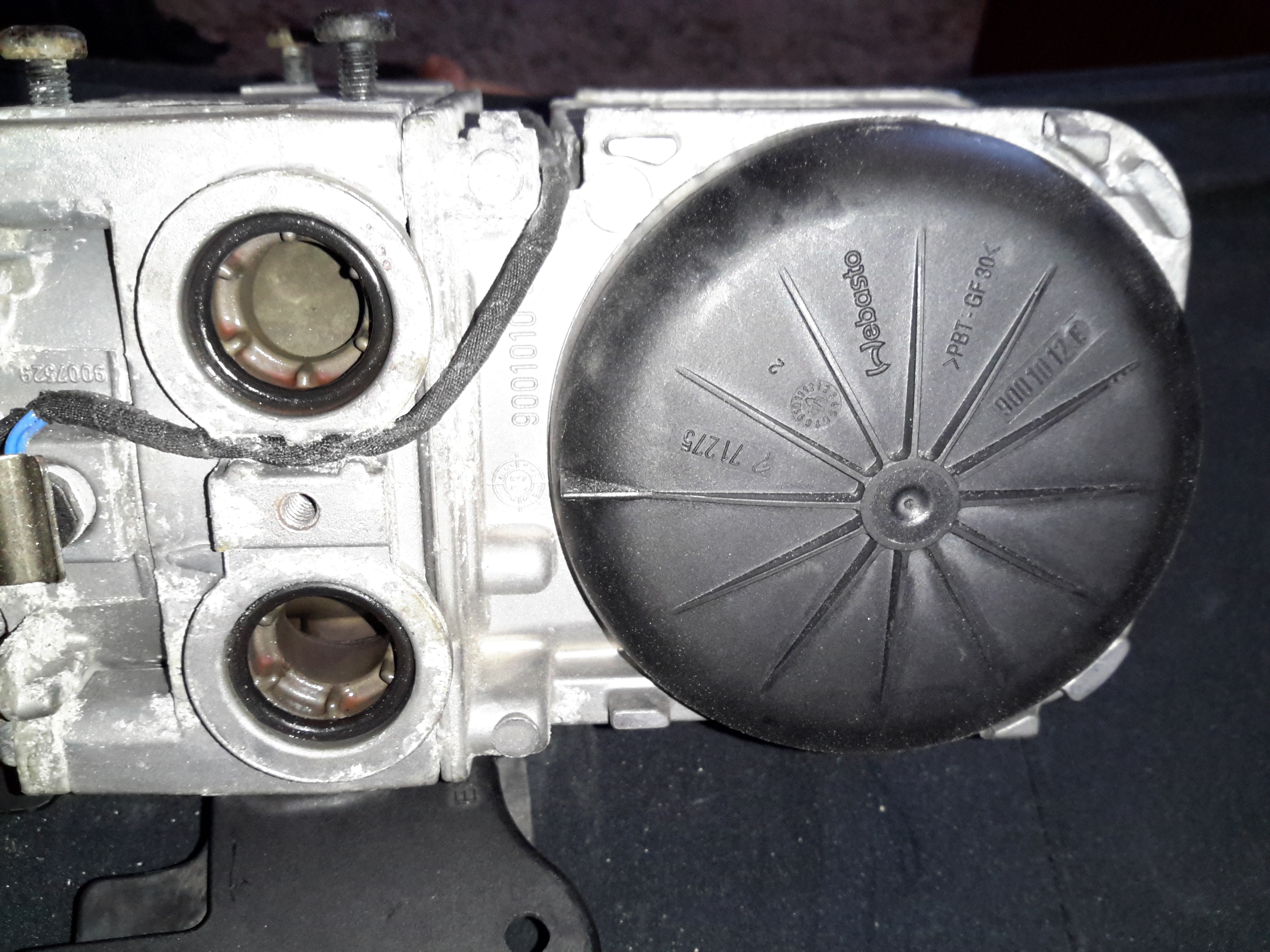
Water Ports & Combustion Fan Cover
Unclipping the cover from the other end reveals the combustion fan, it’s under the black cover. (These are side-channel blowers, to provide the relatively high static pressure required to run the burner).
Sensor Clip
The overheat & temperature sensors are on the end of the heat exchanger, retained by a stainless clip.
Temp & Overheat Sensors
With the clip removed, the sensors can be seen better. There’s some pretty bad corrosion of the aluminium alloy on the end sensor, it’s seized in place.
Burner
The heater splits in half to reveal the evaporative burner itself. I’ve already cleaned the black crud off with a wire brush here, doesn’t look like this heater has seen much use as it’s pretty clean inside.
Burner Chamber
Inside the burner the fuel evaporates & is ignited. There is a brass mesh behind the backplate of the burner to assist with vaporisation.
Glow Plug
The glow plug is fitted into the side of the burner ceramic here. This is probably a Silicon Carbide device. It also acts as a flame sensor when the heater has fired up. The fuel inlet line is to the left under the clamp.
Heat Exhanger
The hot gases from the burner flow into the heat exchanger here, with many fins to increase the surface area. There’s only a couple of mm coating of carbon here, after 10 years on the car I would have expected it to be much more clogged.
I’m currently waiting on some components to build an interface so I can get the Webasto Thermo Test software to talk to the heater. Once this is done I can see if there are any faults logged that need sorting before I can get this heater running, but from the current state it seems to be pretty good visually. More to come once parts arrive!
The full service manual for these heaters can be grabbed from here, along with the wiring details for the Jaguar implementation & the Thermo Test software for talking to them:
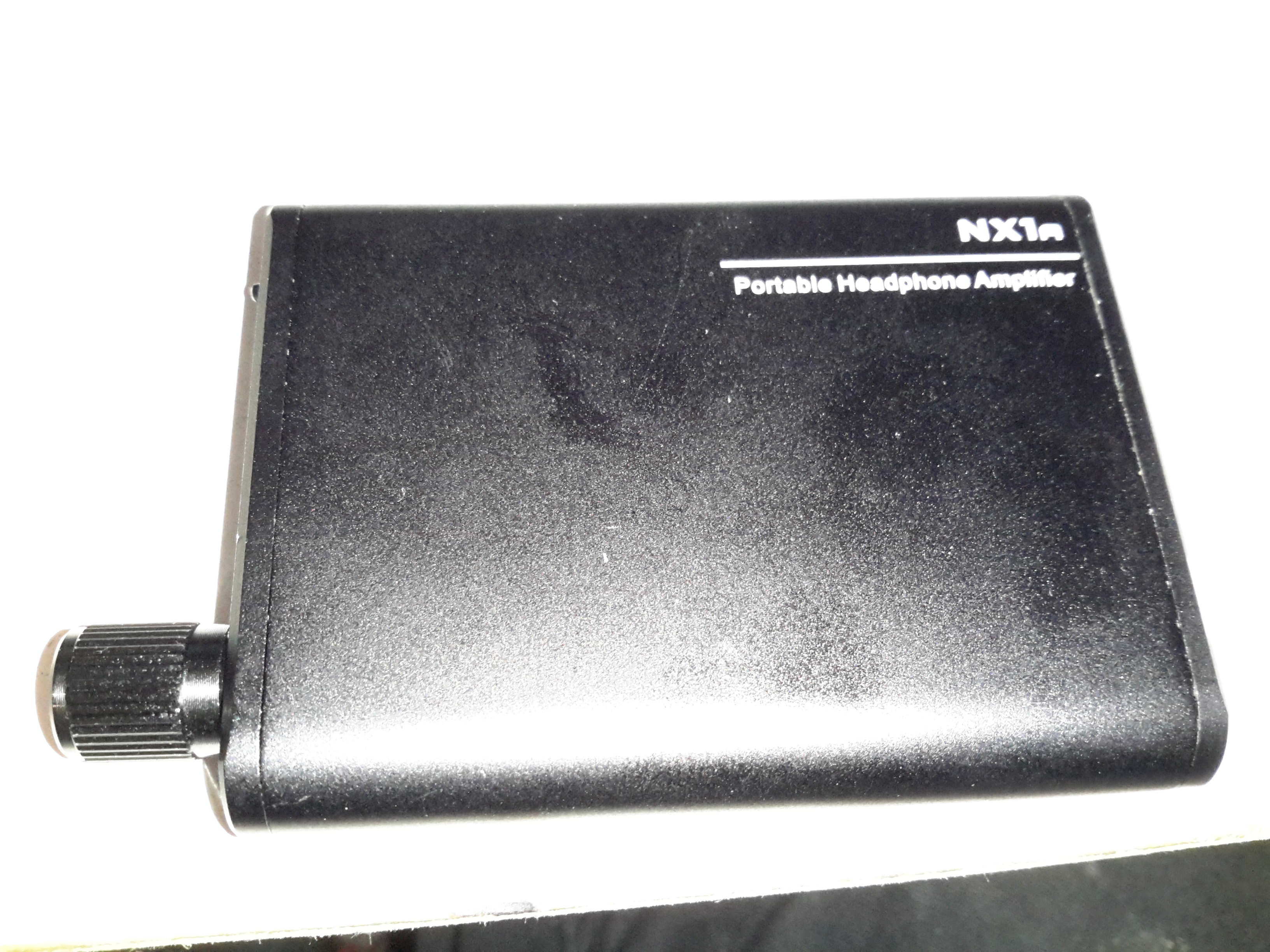
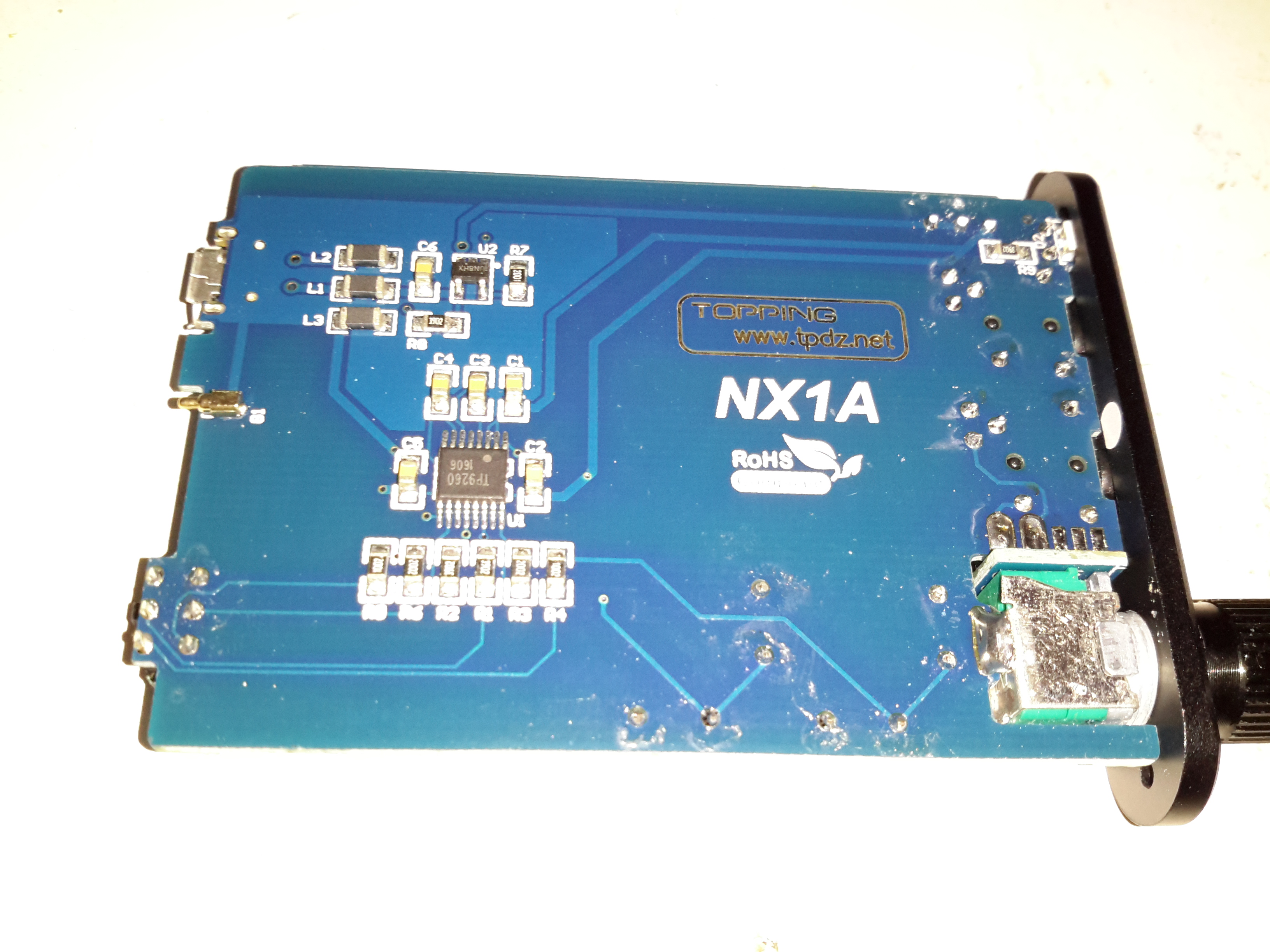
Time for another teardown! Here’s a pocket-sized headphone amplifier for use with mobile devices. This unit is powered by a built-in lithium cell, and can give some pretty impressive volume levels given it’s small size.
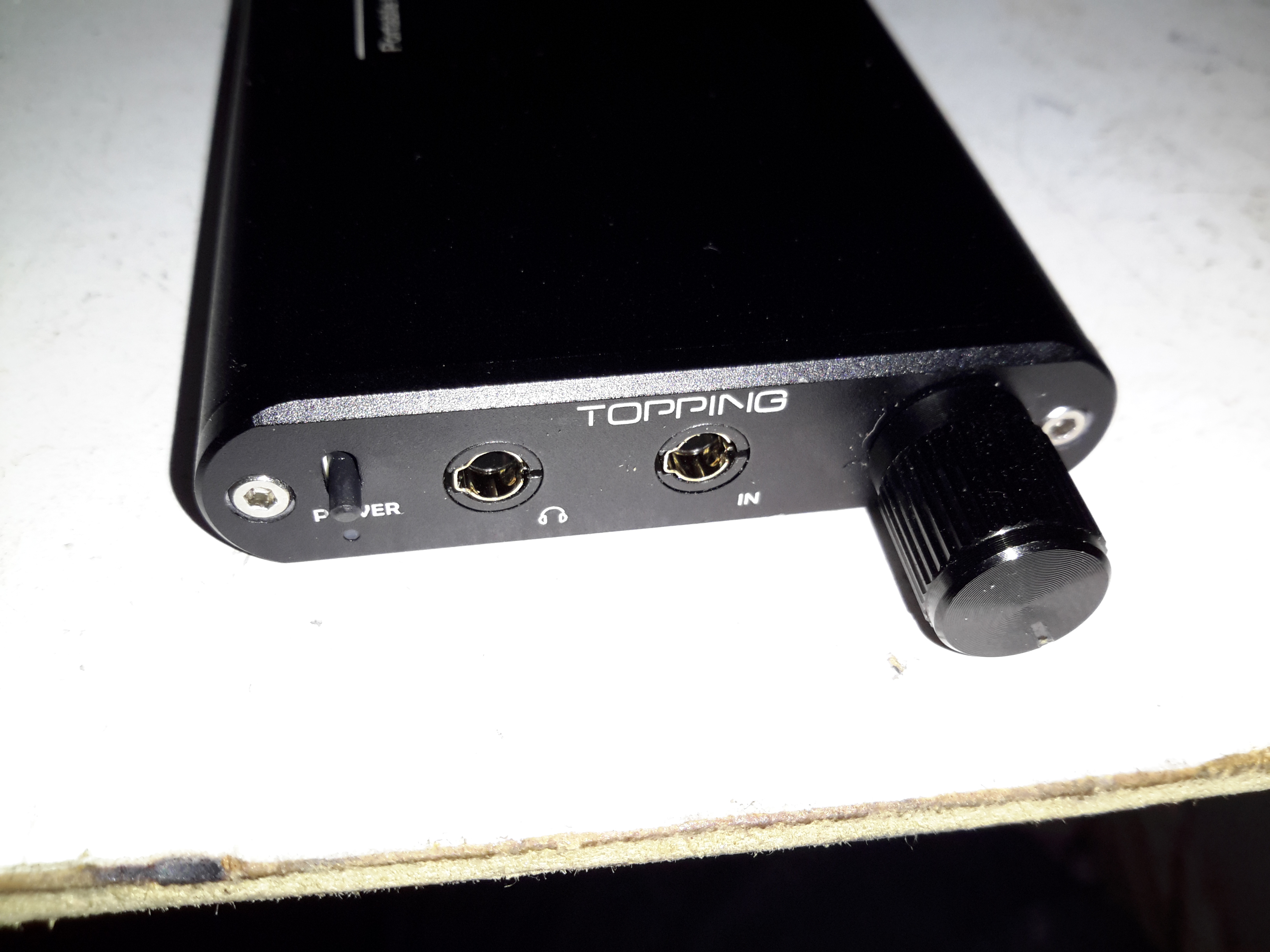
Audio Connections
The 3.5mm audio input & output jacks are on the front of the unit, along with the relatively enormous volume knob & power switch. There’s a little blue LED under the switch that lets the user know when the power is on, but this is a very sedate LED, using very little power.
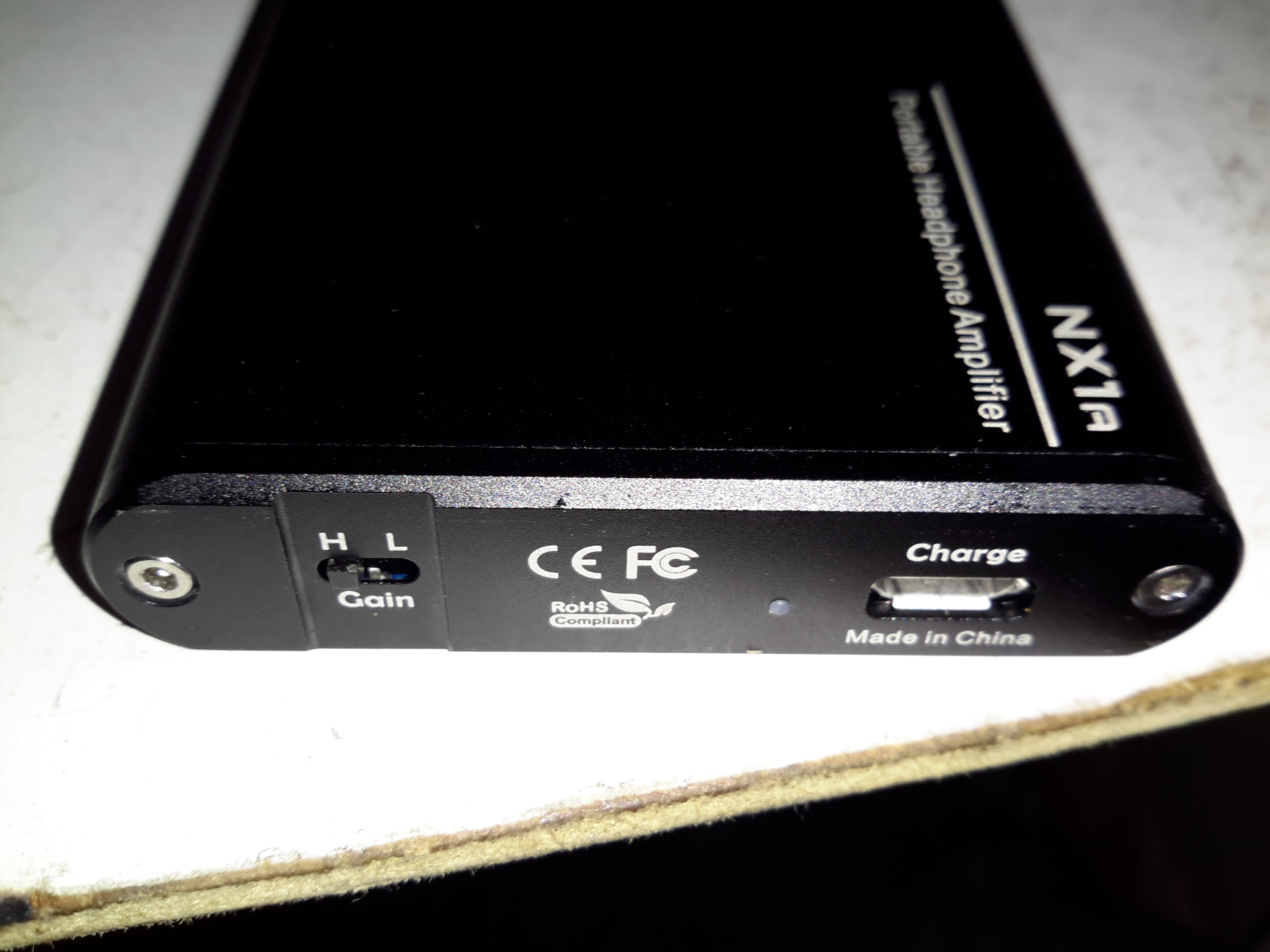
Gain & Charging
On the back is the High-Low gain switch, and the µUSB charging port. There’s another indicator LED to show that the internal cell is charging, in this case a red one.
PCB Top
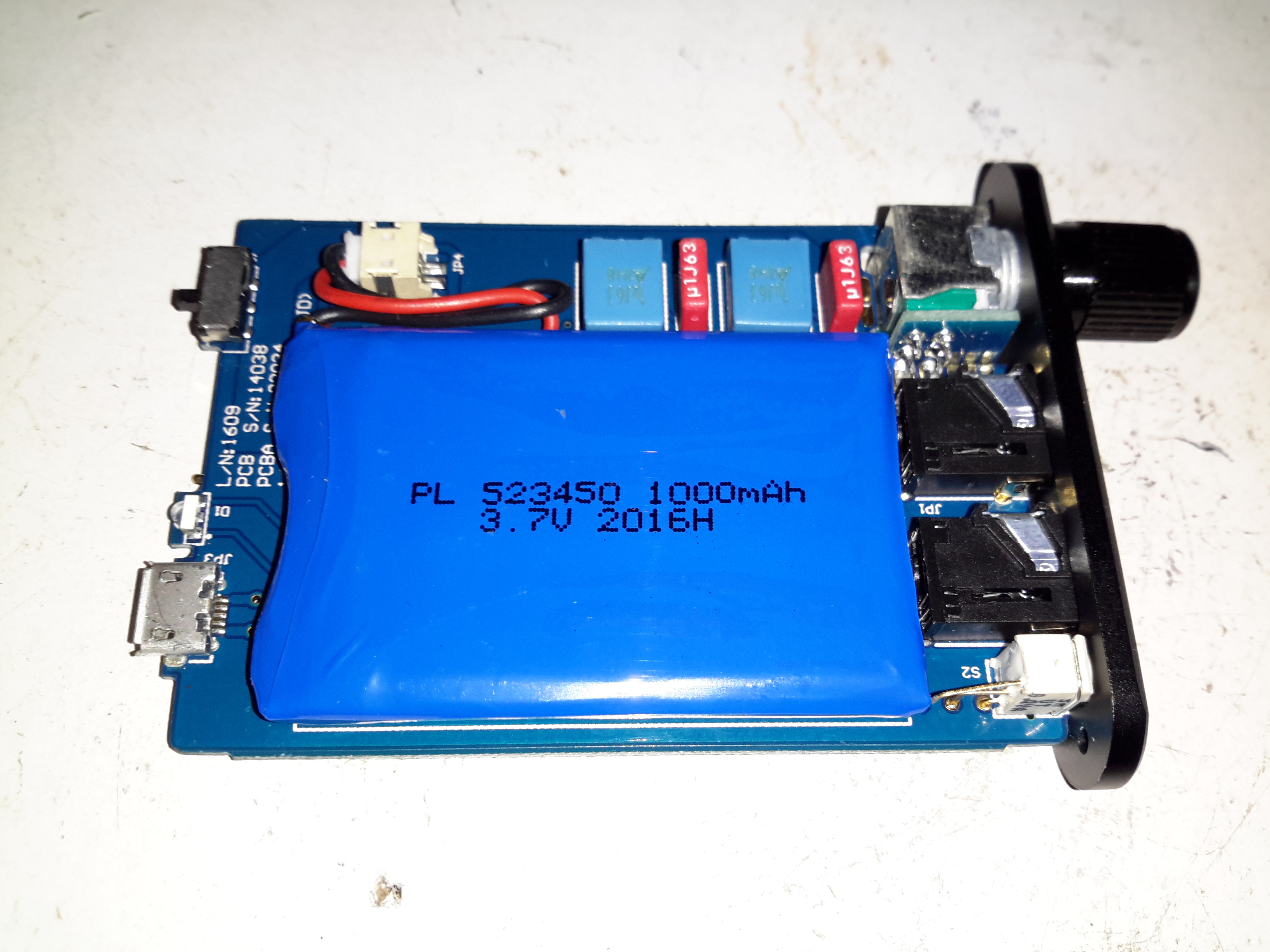
Removing a couple of cap screws allows the internals to slide out of the extruded aluminium casing. Most of the internal space is taken up by the 1Ah lithium cell, here on the top of the PCB secured by some double-sided tape. The volume potentiometer is mounted on a small daughterboard at right angles to get it to fit into the small vertical space in the case.
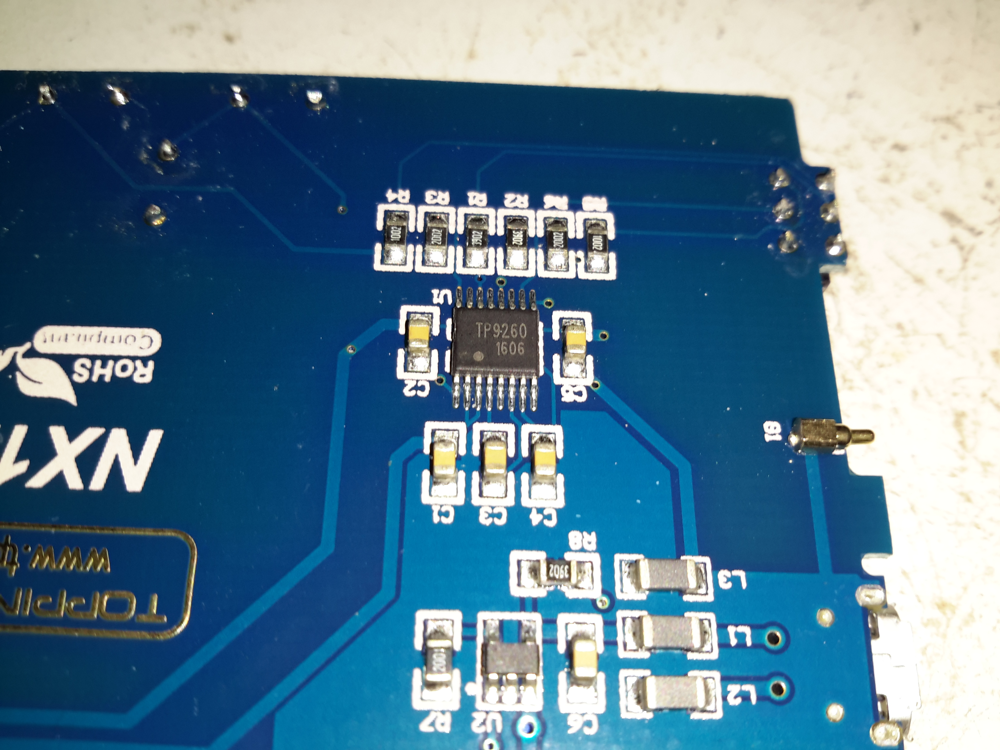
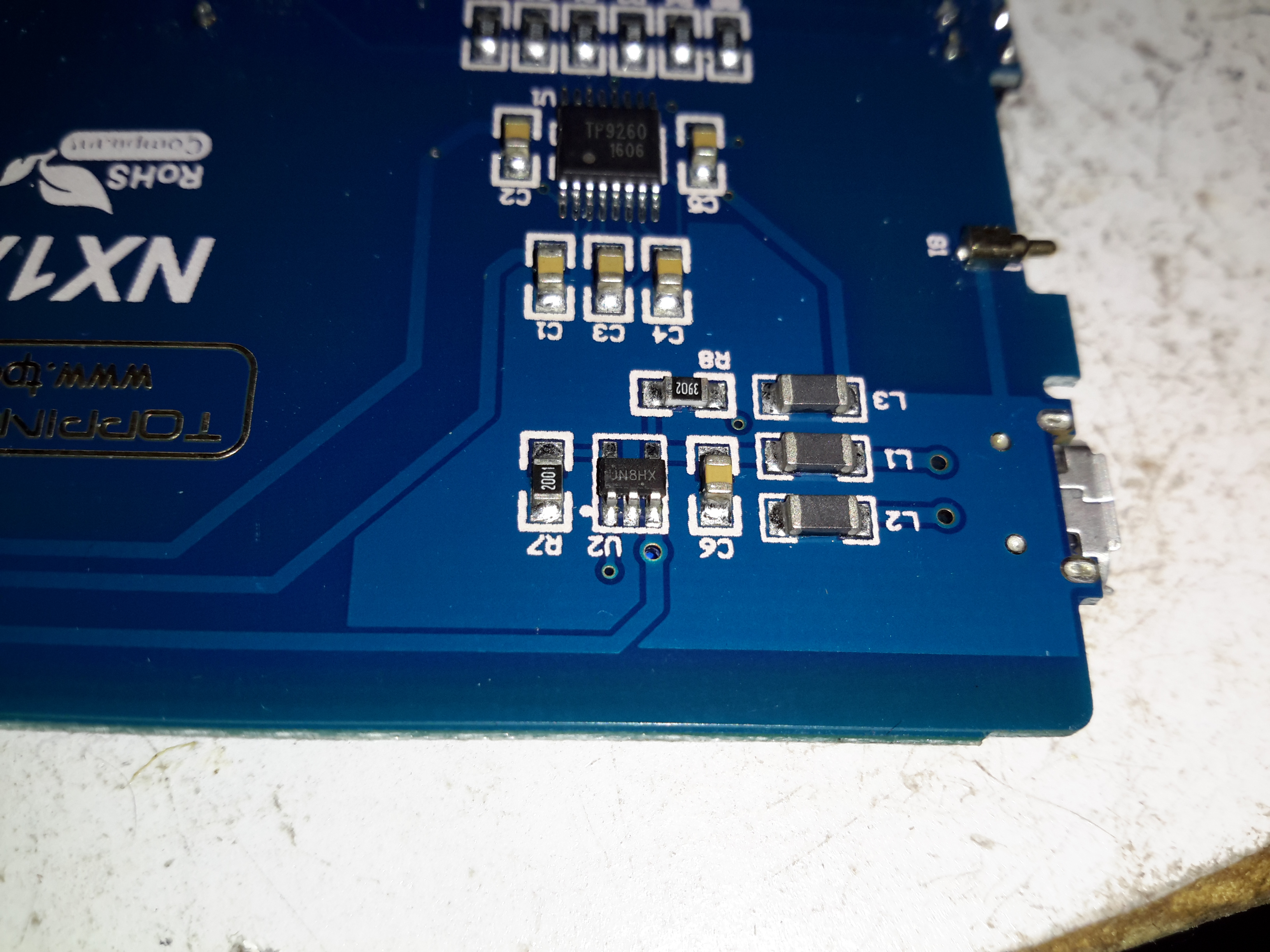
PCB Rear
The bottom of the PCB is equally as sparse – the only ICs being the main audio amp in the centre & the battery charger IC at the top.
Amplifier IC
The main audio amplifier is a TP9260, I couldn’t find a datasheet on this, so I’m unsure of what the specs are. The row of resistors above the IC are for the gain divider circuit. There’s also a pogo pin on the right that makes contact with the back panel of the case for grounding.
Battery Charger
Battery charging is taken care of by a UN8HX 500mA linear charging IC, not much special here.
This little amplifier seems to be pretty well made, considering the price point. The only issue I’ve had so far is the audio cables act like antennas, and when in close proximity to a phone some signal gets picked up & blasted into the headphones as interference.
I recently got the latest upgrade from Virgin Media, 200Mbit DL / 20Mbit UL, and to get this I was informed I’d have to buy their latest hardware, since my existing CPE wouldn’t be able to handle the extra 5Mbit/s upload speed. (My bullshit detector went off pretty hard at that point, as the SuperHub 2 hardware is definitely capable of working fine with 20Mbit/s upload rates). Instead of having to return the old router, I was asked to simply recycle it, so of course the recycling gets done in my pretty unique way!
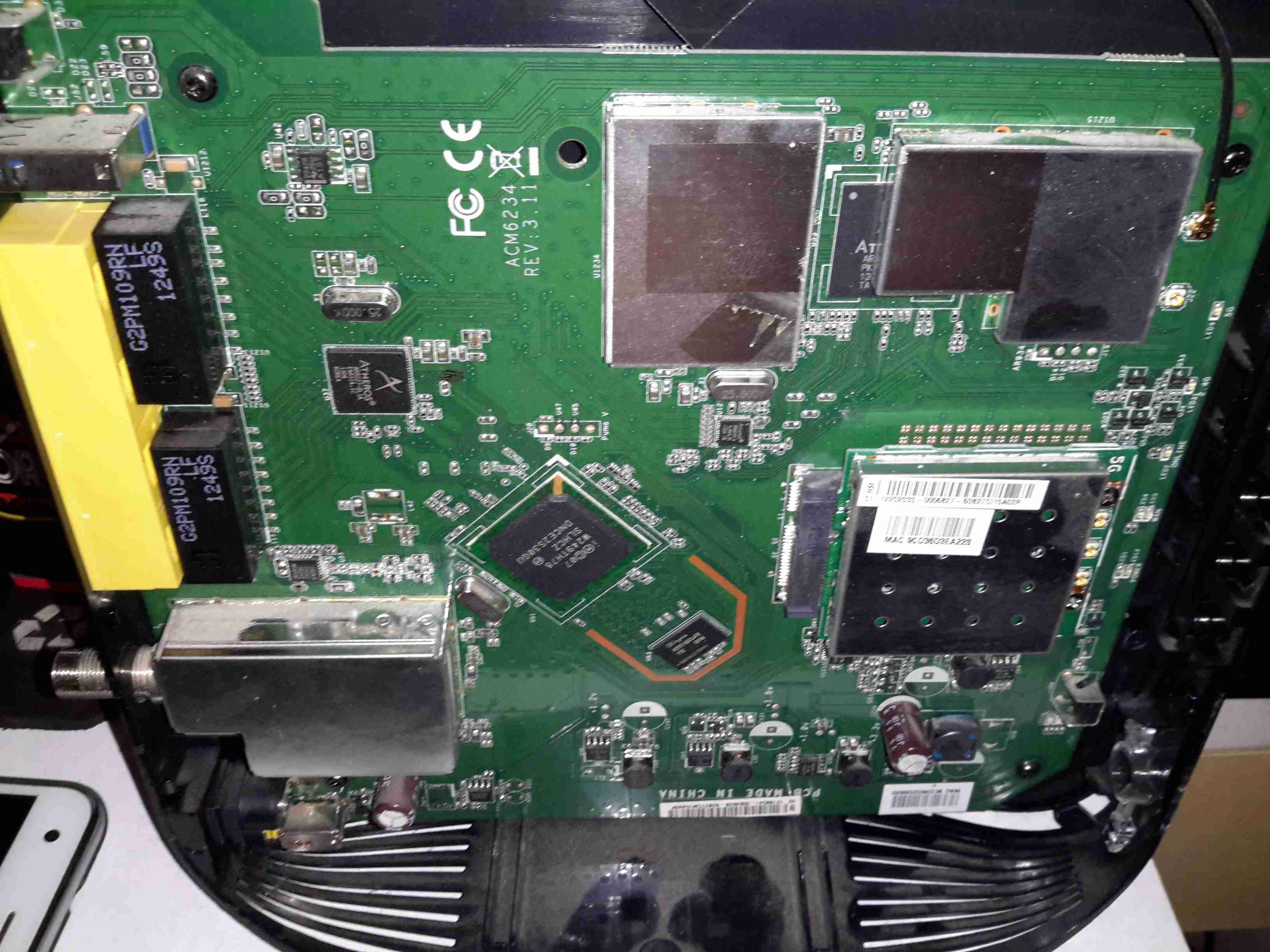
Mainboard
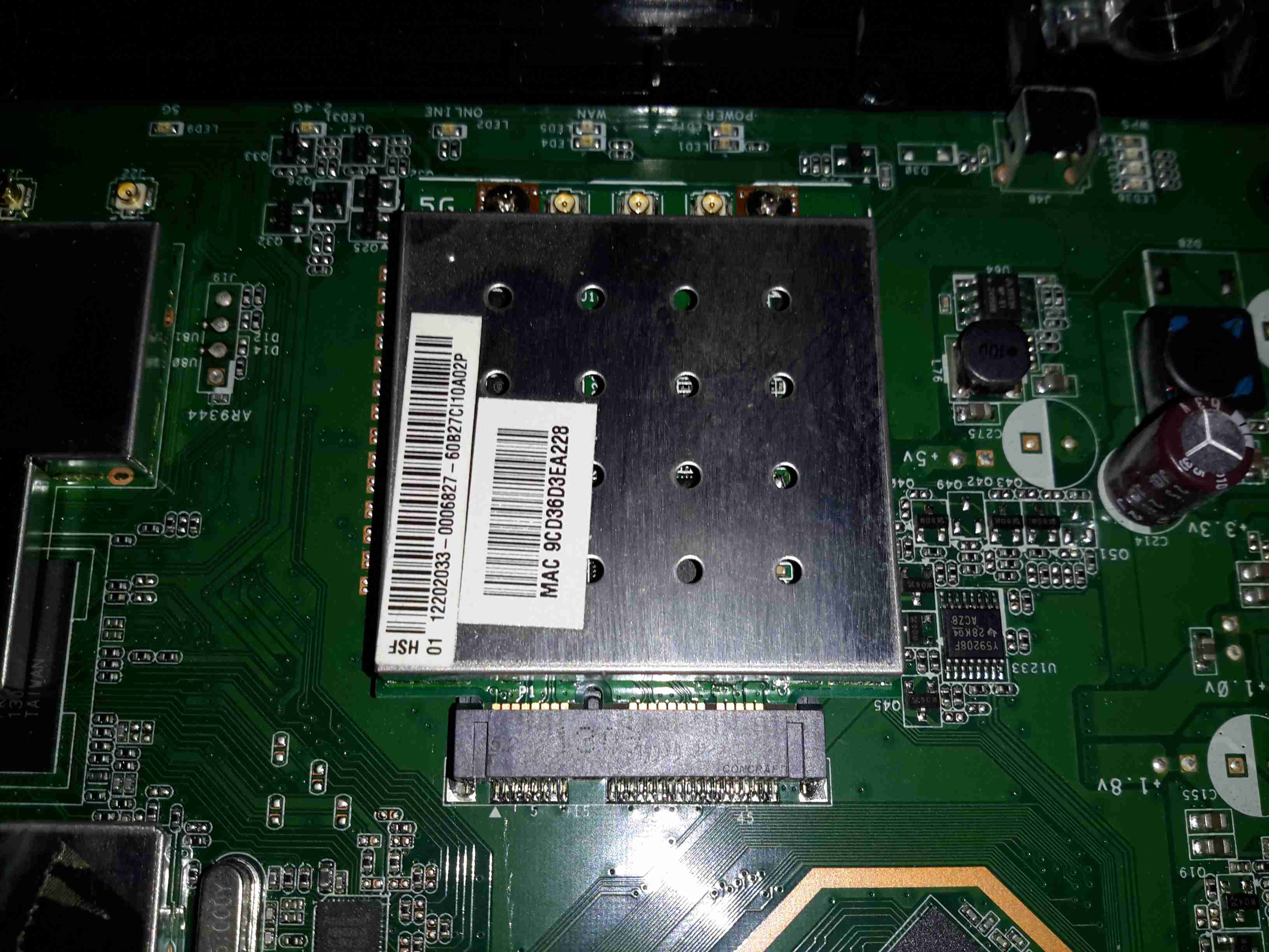
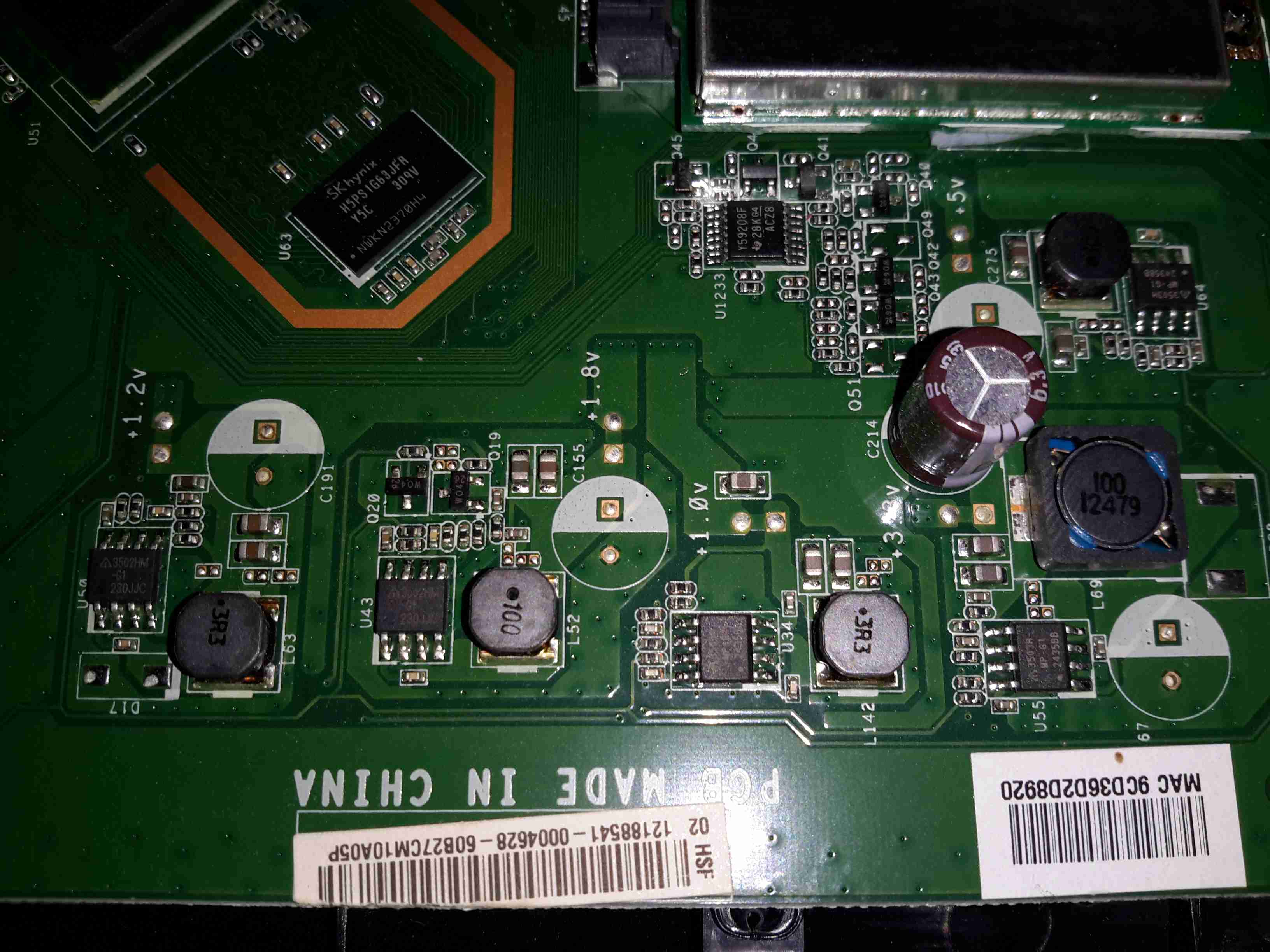
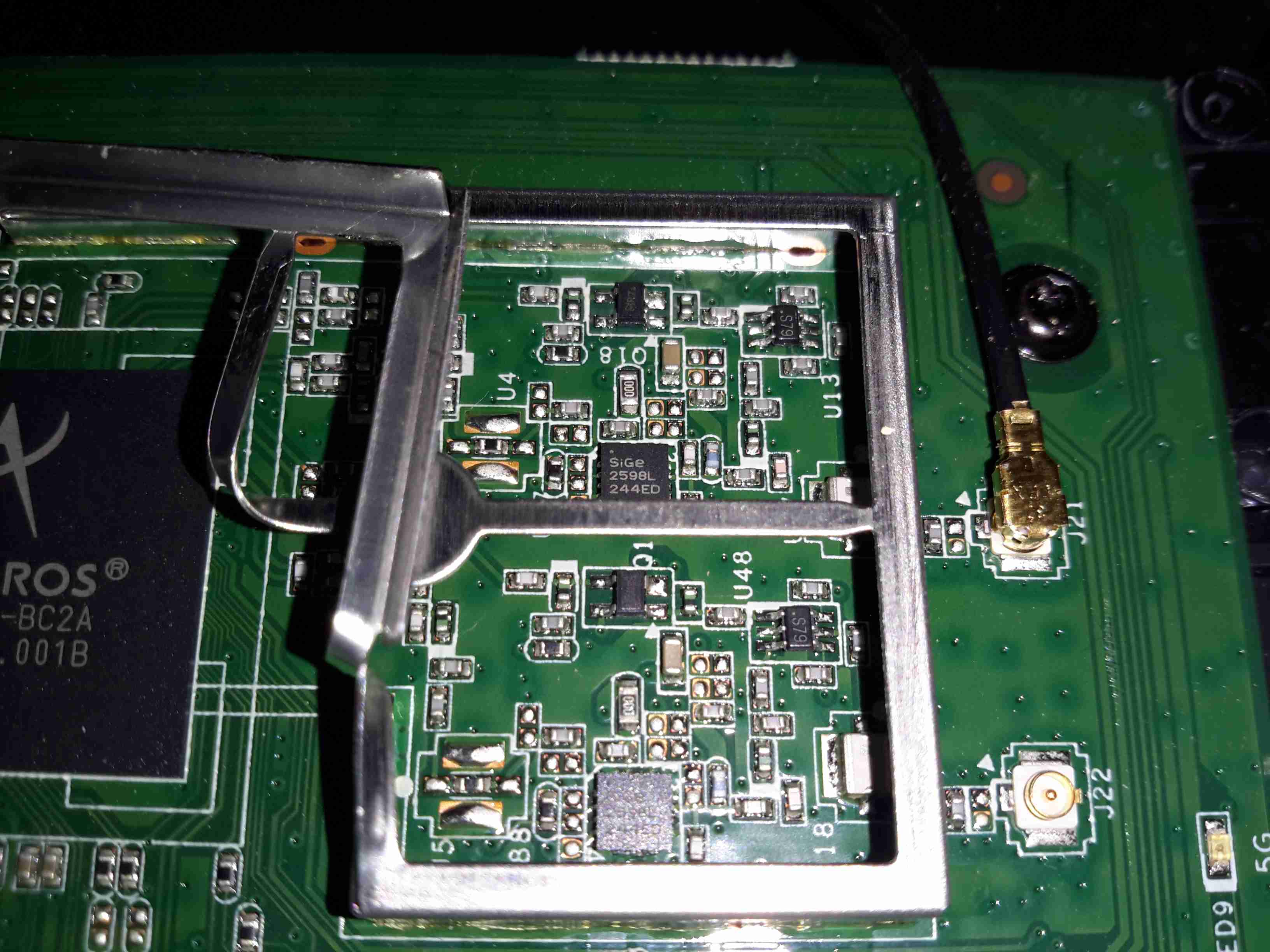
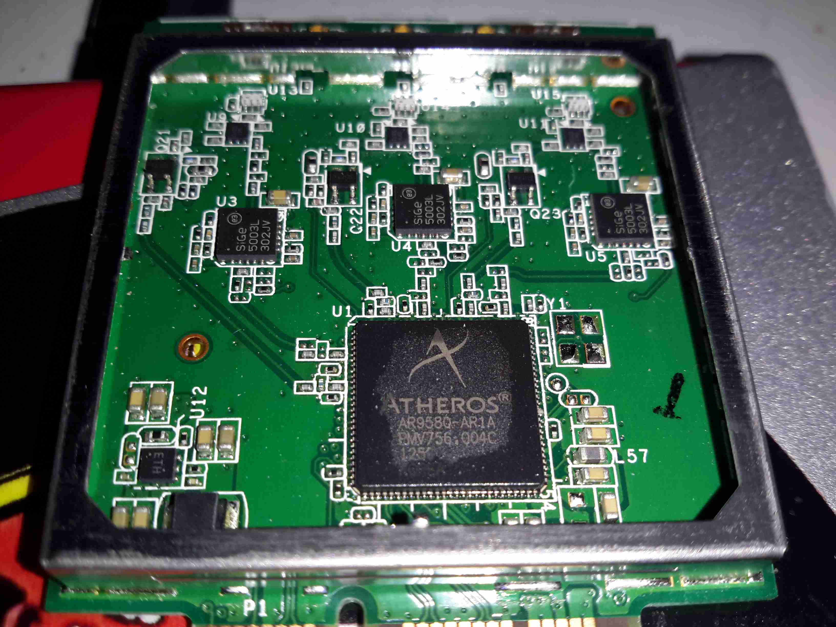
The casing of these units is held together by a single screw & a metric fuckton of plastic clips, disassembly is somewhat hindered by the radio antennas being positioned all over both sides of the casing. Once the side is off, the mainboard is visible. The DOCSIS frontend is lower left, centre is the Intel PUMA 5 Cable Modem SoC with it’s RAM just to the lower right. The right side of the board is taken up by both of the WiFi radio frontends, the 5GHz band being covered by a Mini PCIe card.
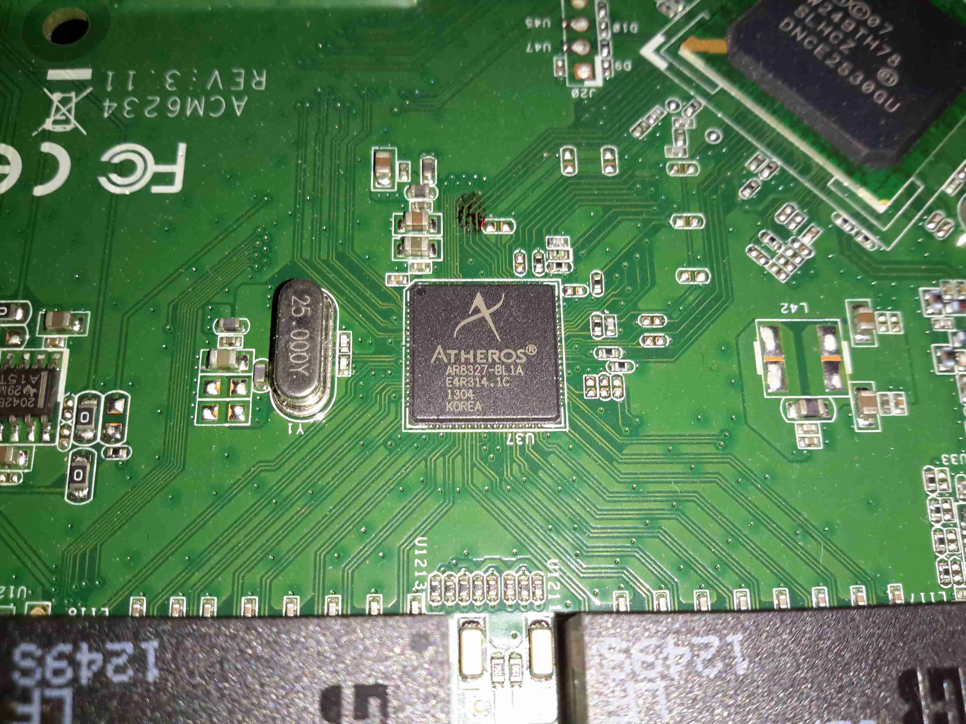
Atheros Gigabit Switch
The 4 gigabit Ethernet ports on the back are serviced by an Atheros AR8327 Managed Layer 3 switch IC, which seems to be a pretty powerful device:
The AR8327 is the latest in high performance small network switching. It is ultra low power, has extensive routing and data management functions and includes hardware NAT functionality (AR8327N). The AR8327/AR8327N is a highly integrated seven-port Gigabit Ethernet switch with a fully non-blocking switch fabric, a high-performance lookup unit supporting 2048 MAC addresses, and a four-traffic class Quality of Service (QoS) engine. The AR8327 has the flexibility to support various networking applications. The AR8327/AR8327N is designed for cost-sensitive switch applications in wireless AP routers, home gateways, and xDSL/cable modem platforms.
Unfortunately most of the features of this router are locked out by VM’s extremely restrictive firmware. With any of their devices, sticking the VM supplied unit into modem mode & using a proper router after is definitely advised!
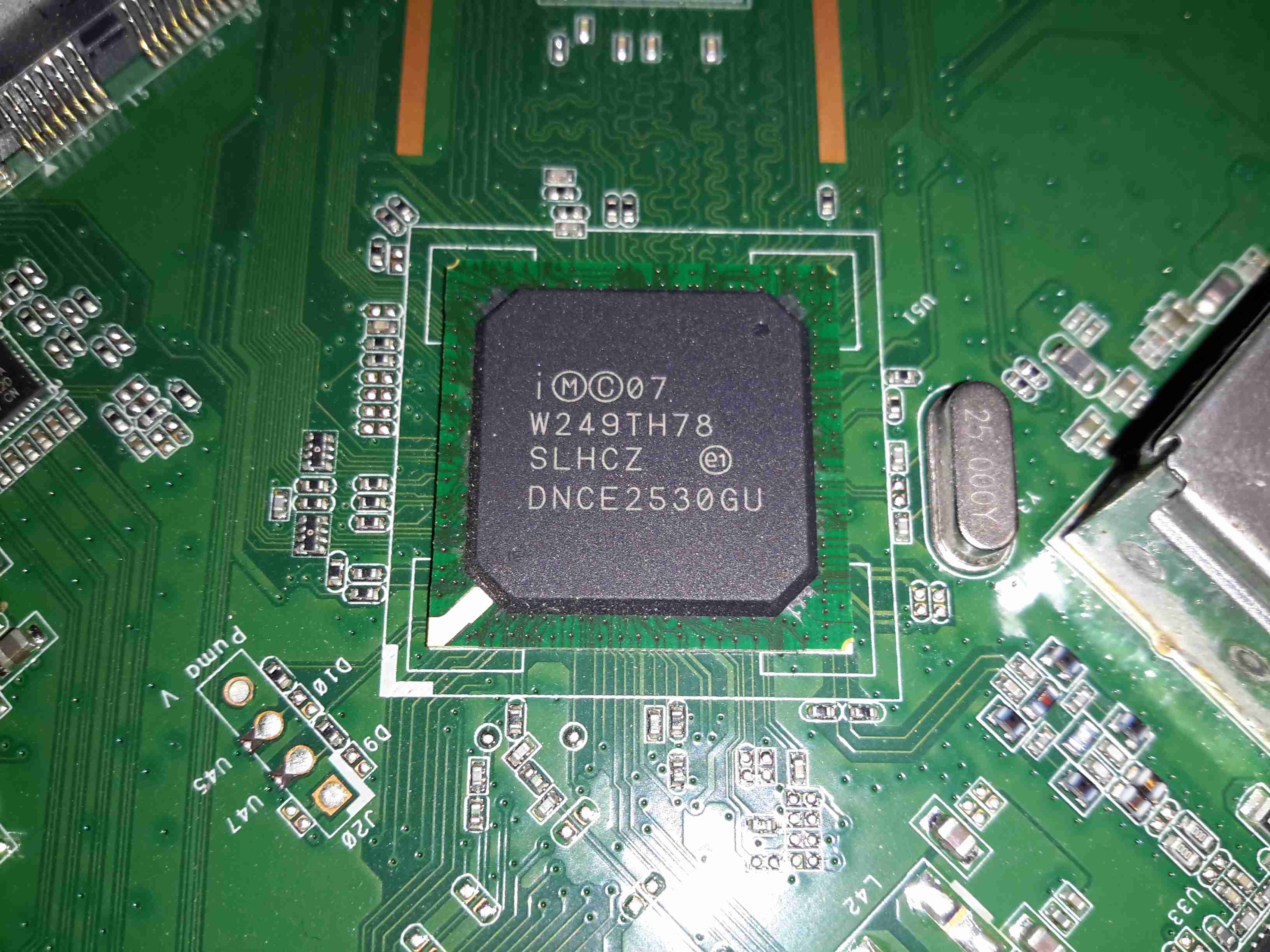
Intel Puma 5 CM CPU
The cable modem side of things is taken care of by the Intel PUMA 5 DNCE2530GU SoC. This appears to communicate with the rest of the system via the Ethernet switch & PCI Express for the 5GHz radio.
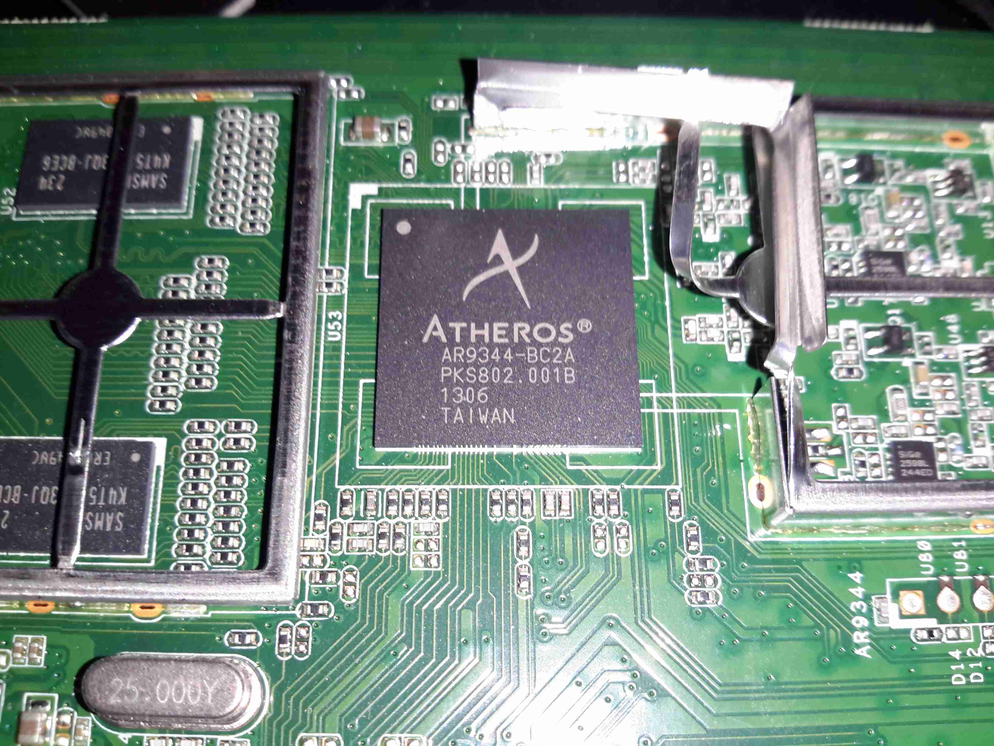
Atheros WiFi SoC
The 2.4GHz radio functionality is supplied by an Atheros AR9344 SoC, it’s RAM is to the left. This is probably handling all the router functions of this unit, but I can’t be certain.
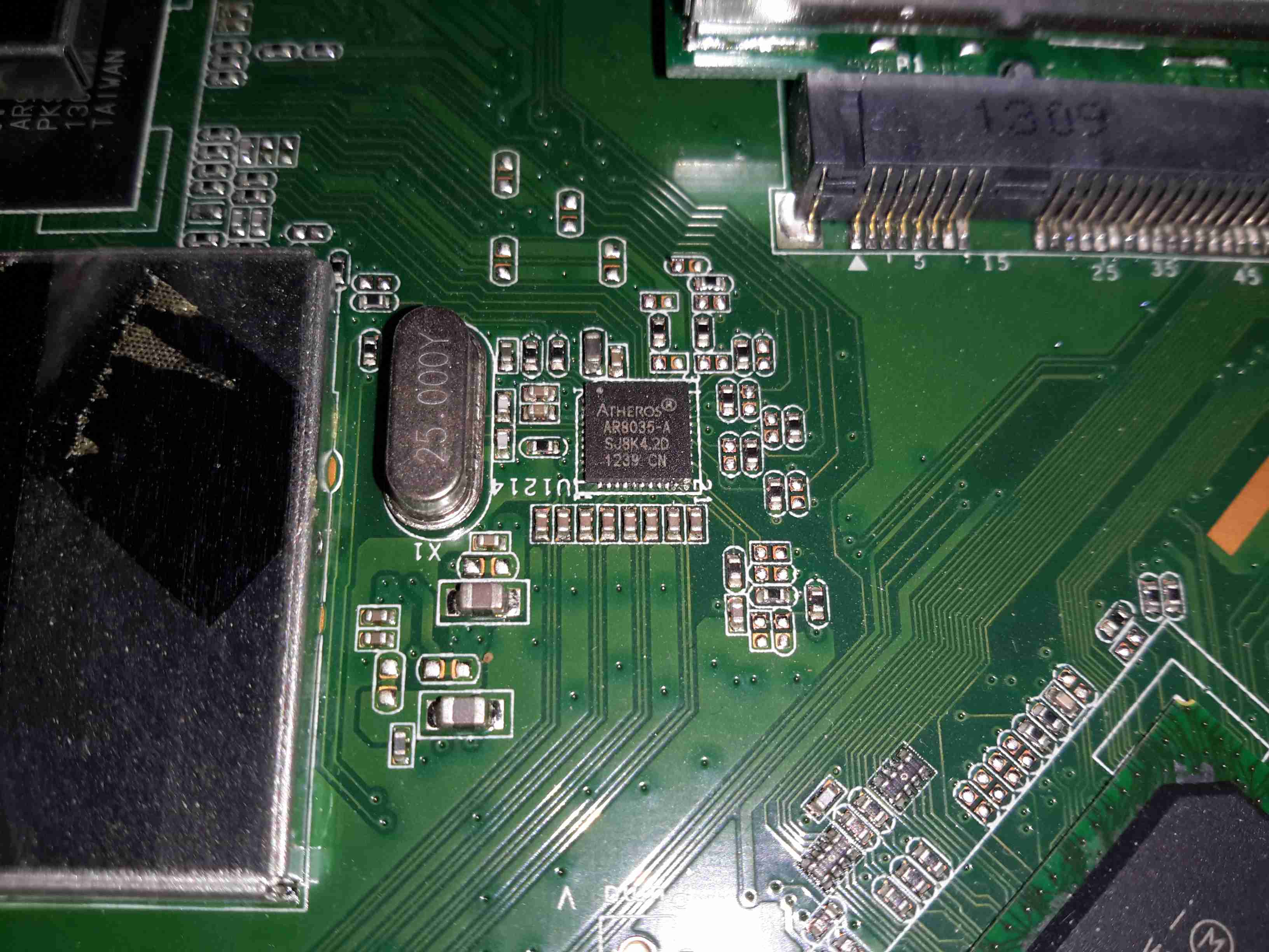
Atheros LAN PHY
A separate Ethernet PHY is located between the SoC & the switch IC.
5GHz Radio Card
The 5GHz band is served by a totally separate radio module, in Mini PCIe format, although it’s a bit wider than standard. This module will probably be kept for reuse in another application.
Power Supplies
All down the edge of the board are the multiple DC-DC converters to generate the required voltage rails.
MaxLinear MXL261 Frontend
The DOCSIS frontend is handled by a MaxLinar MXL261 Tuner/Demodulator. More on this IC in my decapping post 🙂
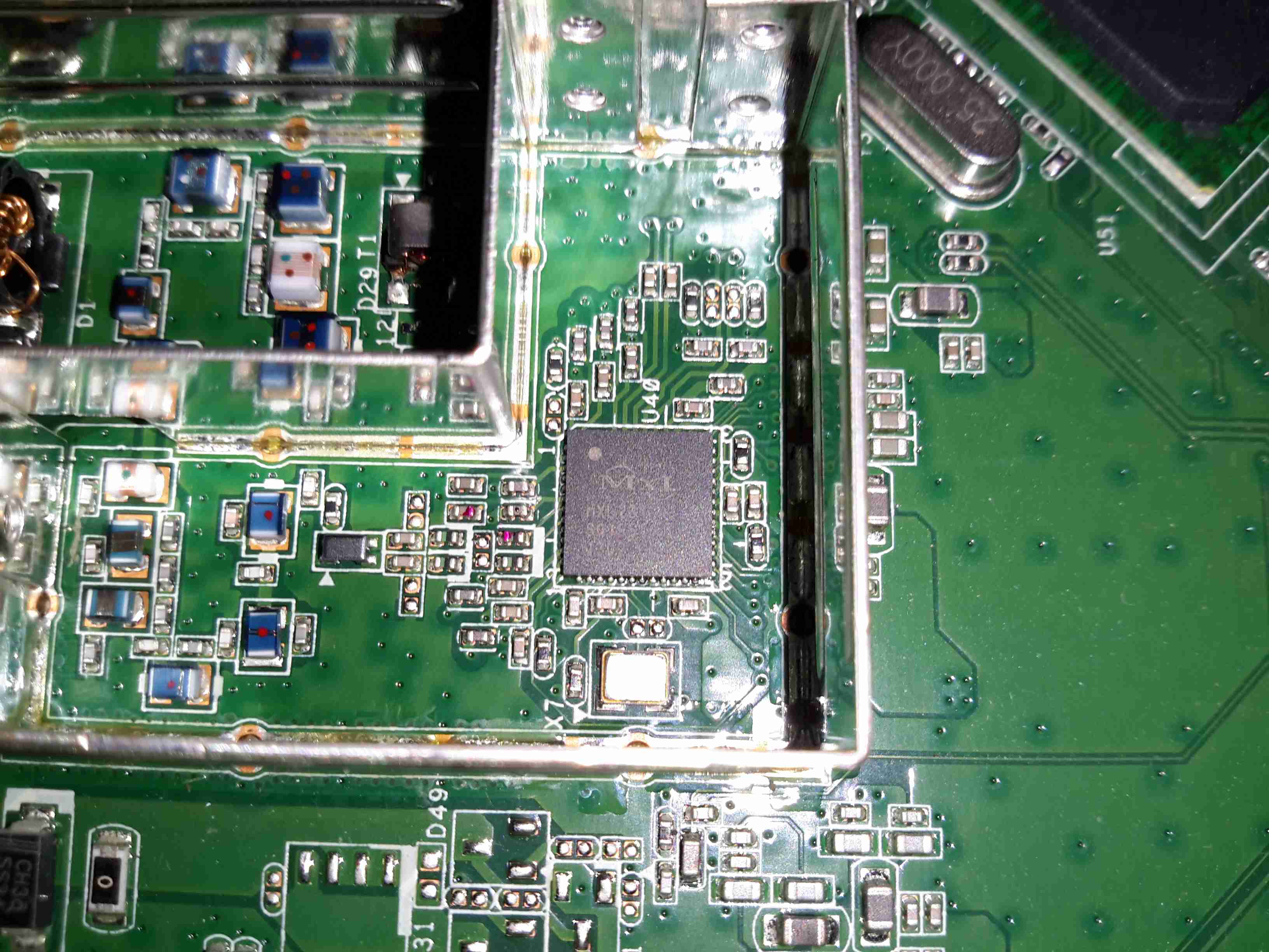
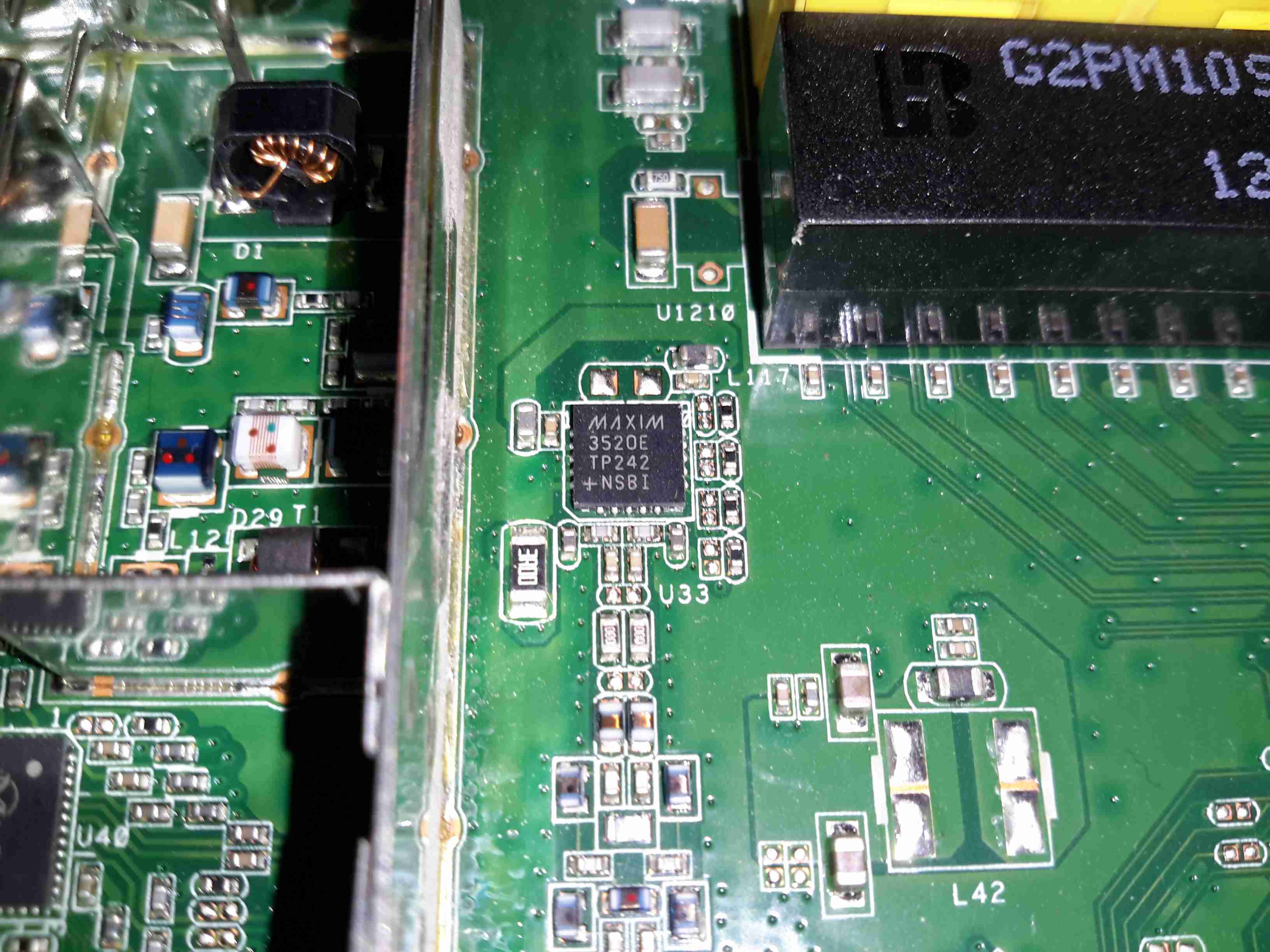
The Unknown One
I’ve honestly no idea what on earth this Maxim component is doing. It’s clearly connected via an impedance matched pair, and that track above the IC looks like an antenna, but nothing I search for brings up a workable part number.
2.4GHz Frontend
The RF switching & TX amplifiers are under a shield, these PA chips are SiGe parts.
Atheros 5GHz Radio
Pretty much the same for the 5GHz radio, but with 3 radio channels.
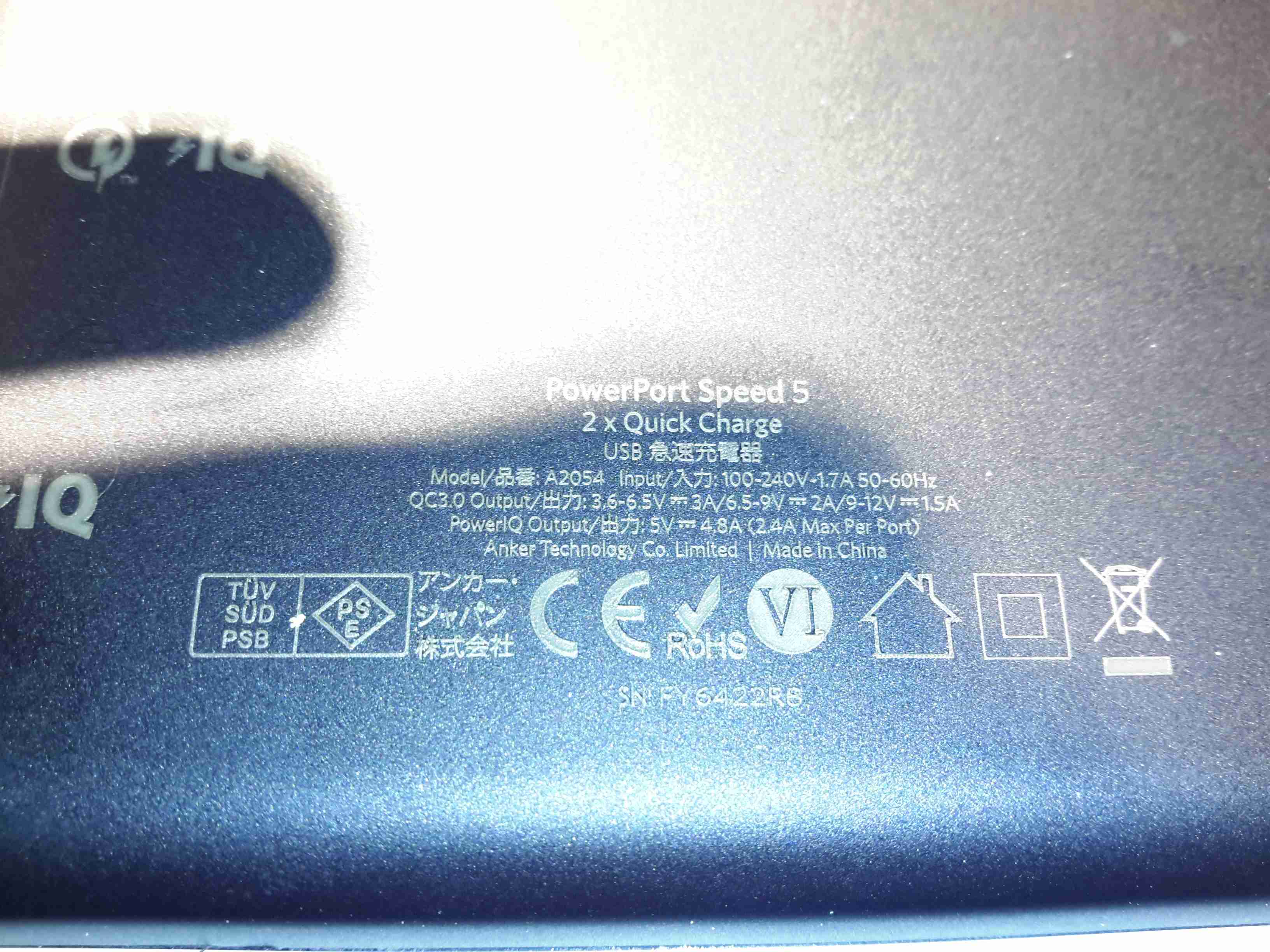
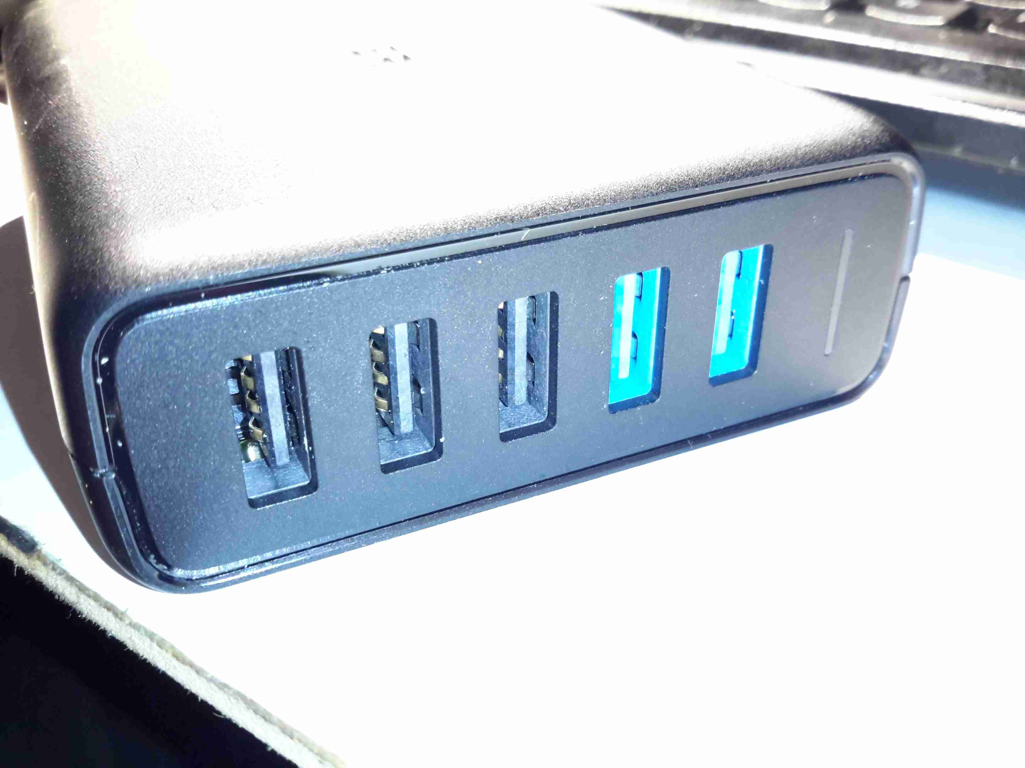
Here’s a piece of tech that is growing all the more important in recent times, with devices with huge battery capacities, a quick charger. This unit supports Qualcomm’s Quick Charge 3 standard, where the device being charged can negotiate with the charger for a higher-power link, by increasing the bus voltage past the usual 5v.
Rear
The casing feels rather nice on this unit, sturdy & well designed. All the legends on the case are laser marked, apart from the front side logo which is part of the injection moulding.
Specifications
The power capacity of this charger is pretty impressive, with outputs for QC3 from 3.6-6.5v at 3A, up to 12v 1.5A. Standard USB charging is limited at 4.8A for the other 3 ports.
Ports
The two of the 5 USB ports are colour coded blue on the QC3 ports. The other 3 are standard 5v ports, the only thing that doesn’t make sense in the ratings is the overall current rating of the 5v supply (4.8A), and the rated current of each of the ports (2.4A) – this is 7.2A total rather than 4.8A.
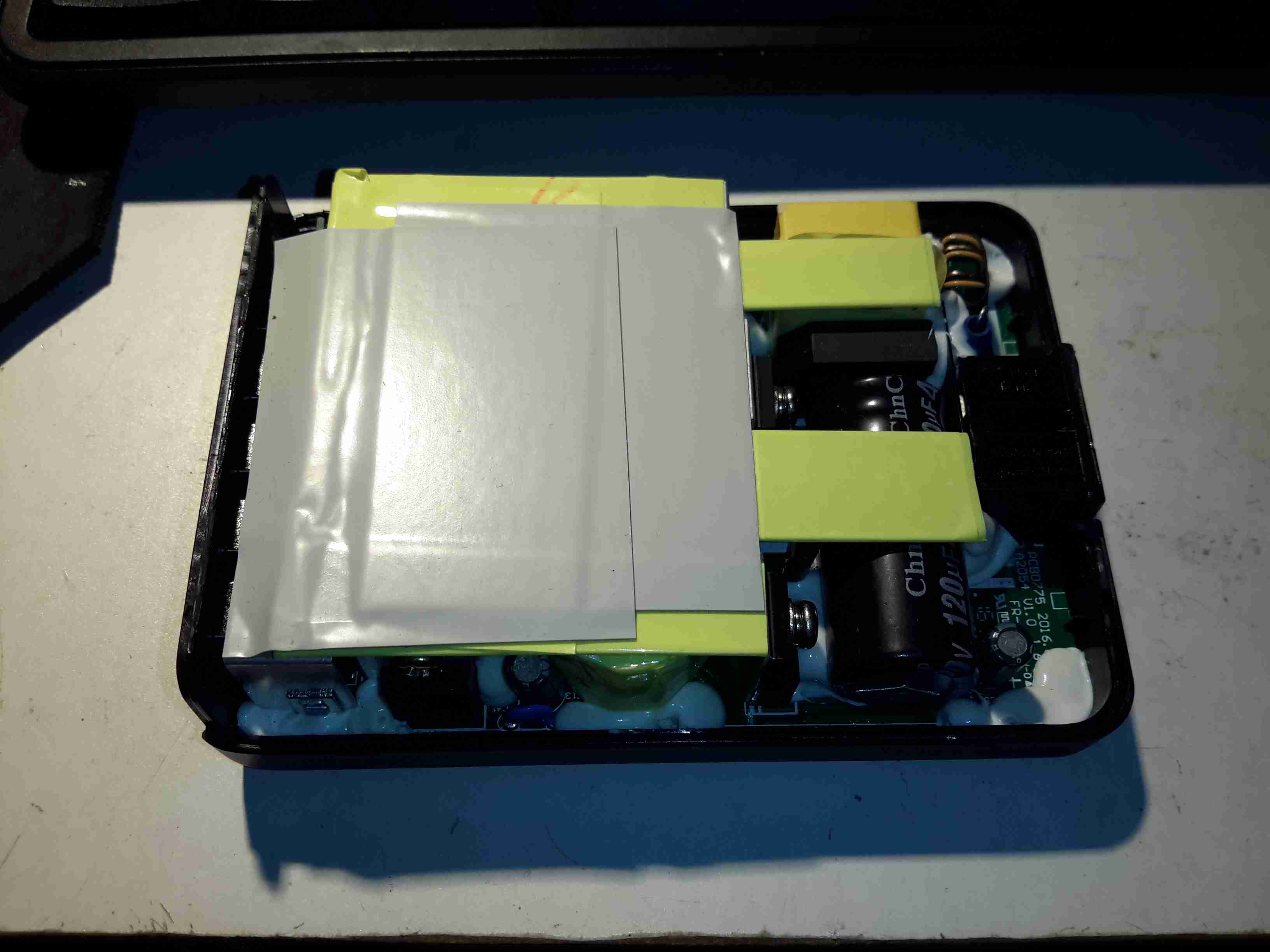
Top Removed
The casing is glued together at the seam, but it gave in to some percussive attack with a screwdriver handle. The inside of this supply is mostly hidden by the large heatspreader on the top.
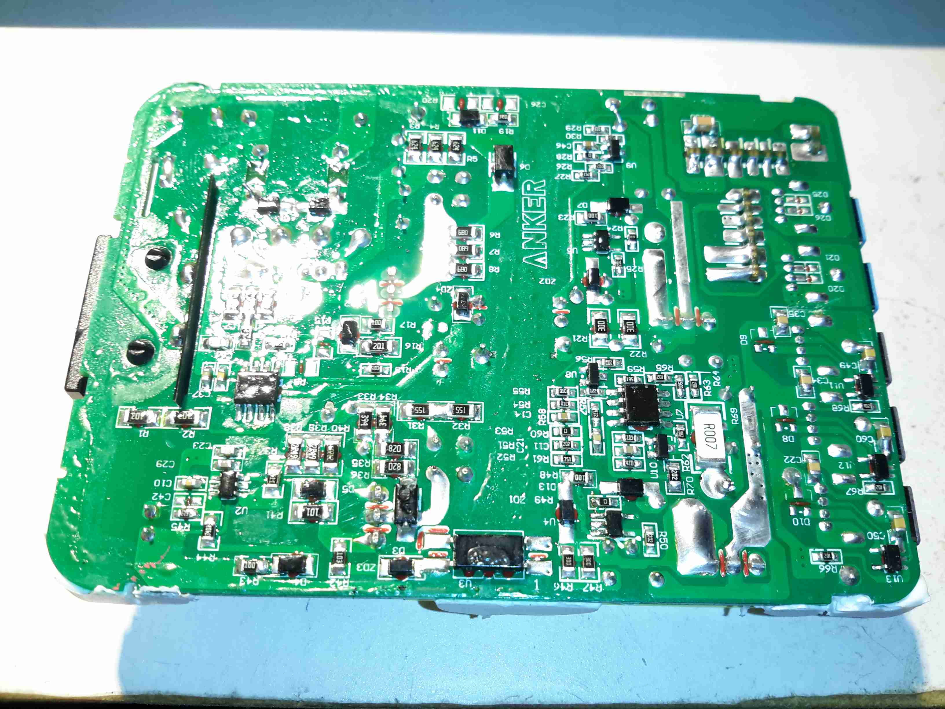
Main PCB Bottom
This is a nicely designed board, the creepage distances are at least 8mm between the primary & secondary sides, the bottom also has a conformal coating, with extra silicone around the primary-side switching transistor pins, presumably to decrease the chances of the board flashing over between the close pins.
On the lower 3 USB ports can be seen the 3 SOT-23 USB charge control ICs. These are probably similar to the Texas Instruments TPS2514 controllers, which I’ve experimented with before, however I can’t read the numbers due to the conformal coating. The other semiconductors on this side of the board are part of the voltage feedback circuits for the SMPS. The 5v supply optocoupler is in the centre bottom of the board.
Heatsink Removed
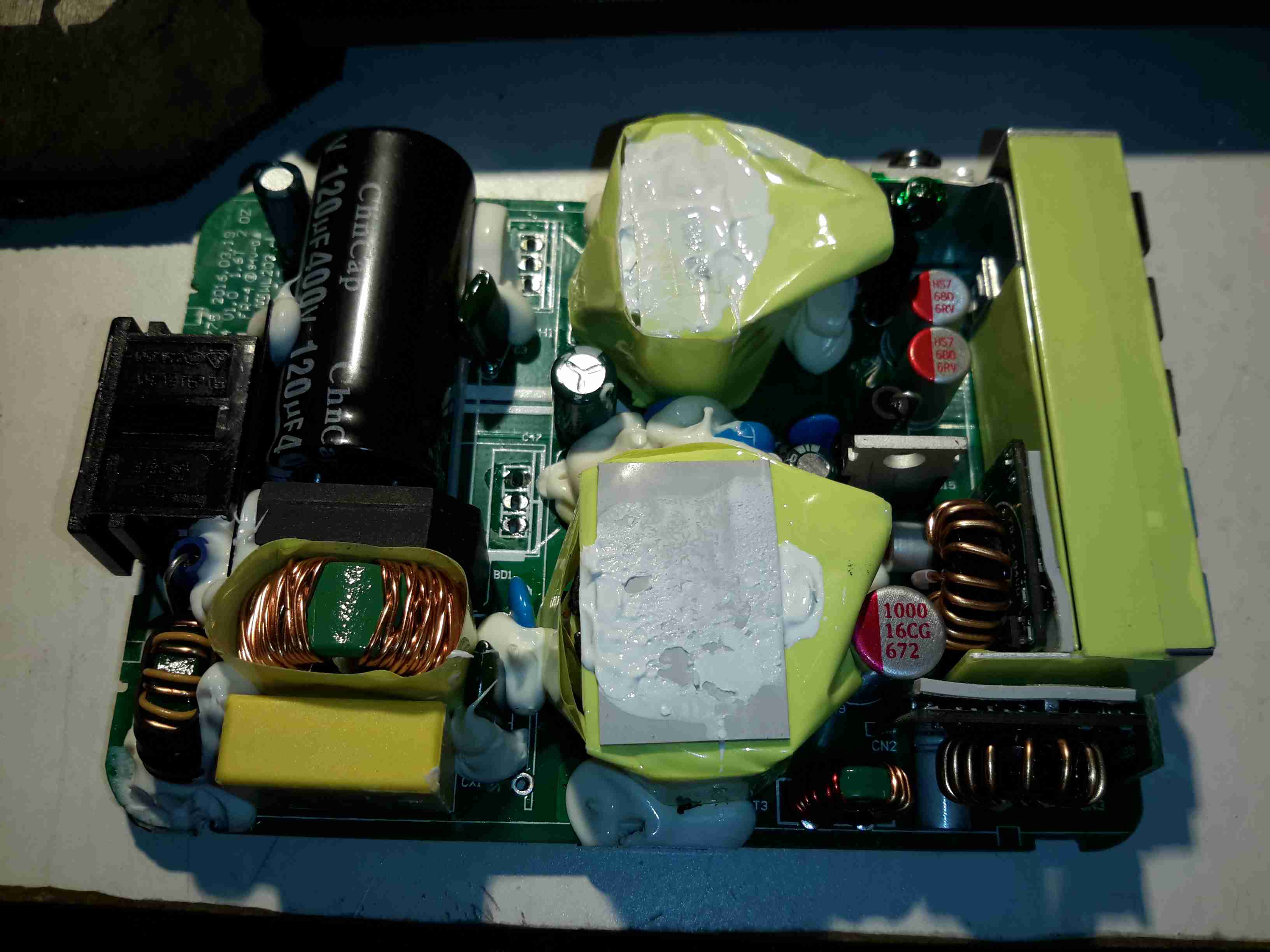
Desoldering the pair of primary side transistors allowed me to easily remove the heatspreader from the supply. There’s thermal pads & grease over everything to get rid of the heat. Here can be seen there are two transformers, forming completely separate supplies for the standard USB side of things & the QC3 side. Measuring the voltages on the main filter capacitors showed me the difference – the QC3 supply is held at 14.2v, and is managed through other circuits further on in the power chain. There’s plenty of mains filtering on the input, as well as common-mode chokes on the DC outputs before they reach the USB ports.
Quick Charge 3 DC-DC Converters
Here’s where the QC3 magic happens, a small DC-DC buck converter for each of the two ports. The data lines are also connected to these modules, so all the control logic is located on these too. The TO-220 device to the left is the main rectifier.
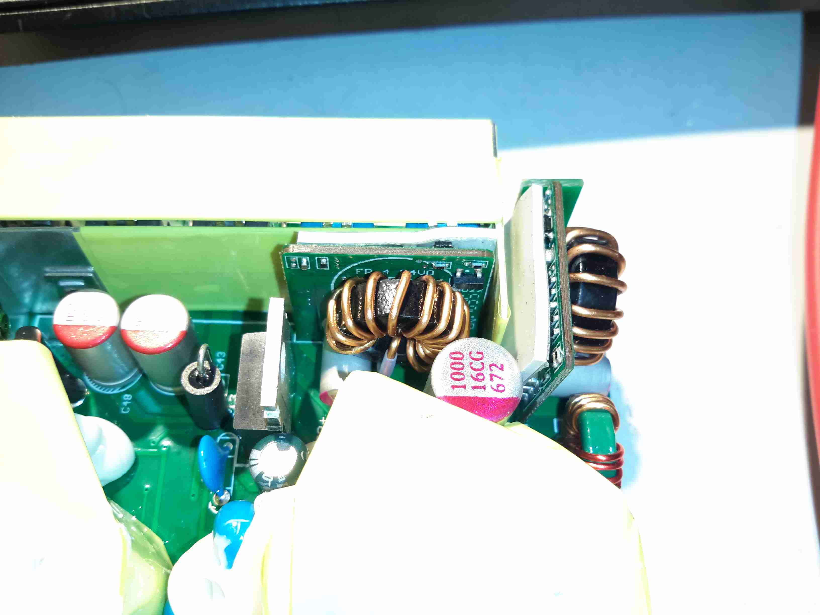
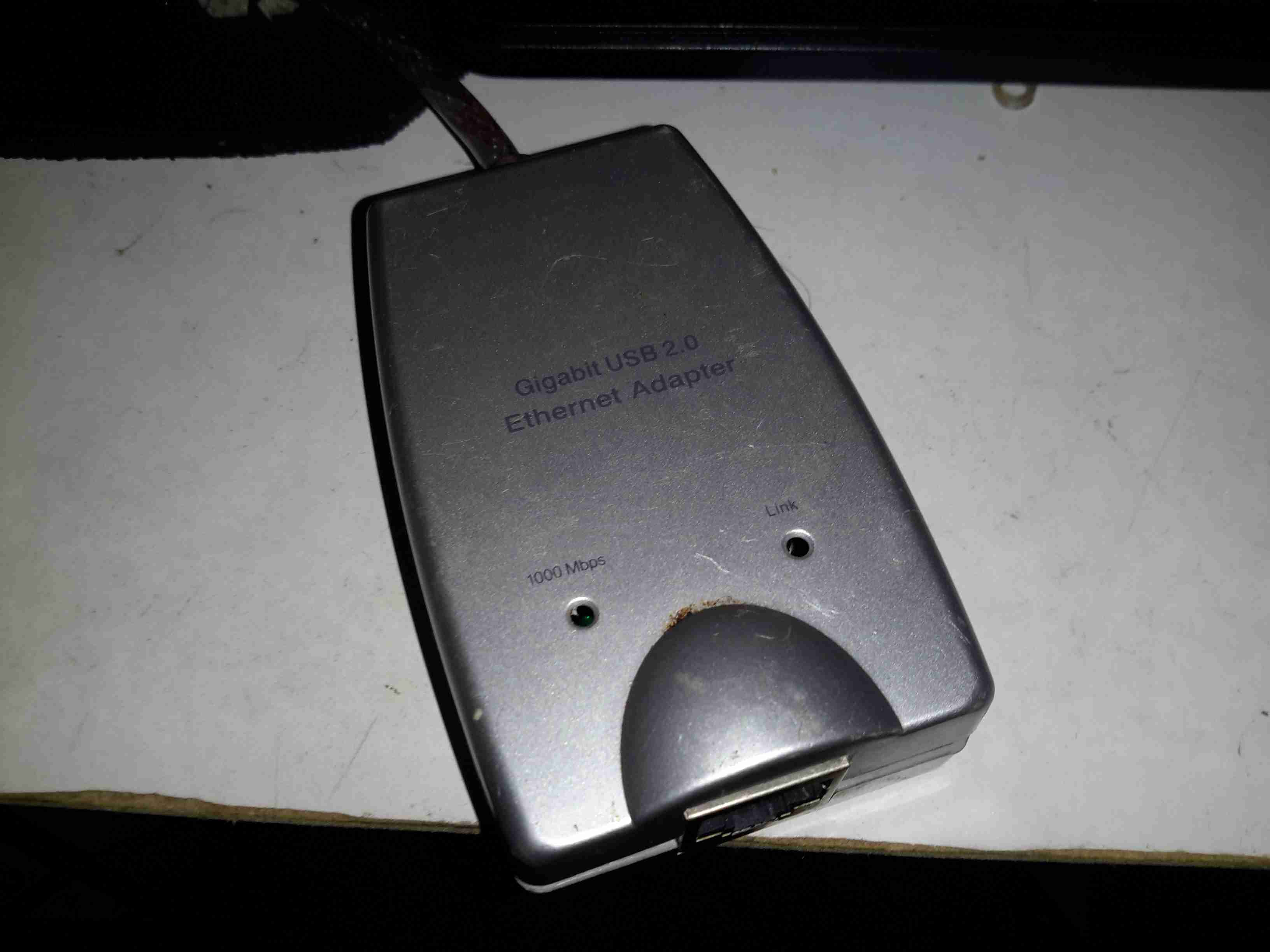
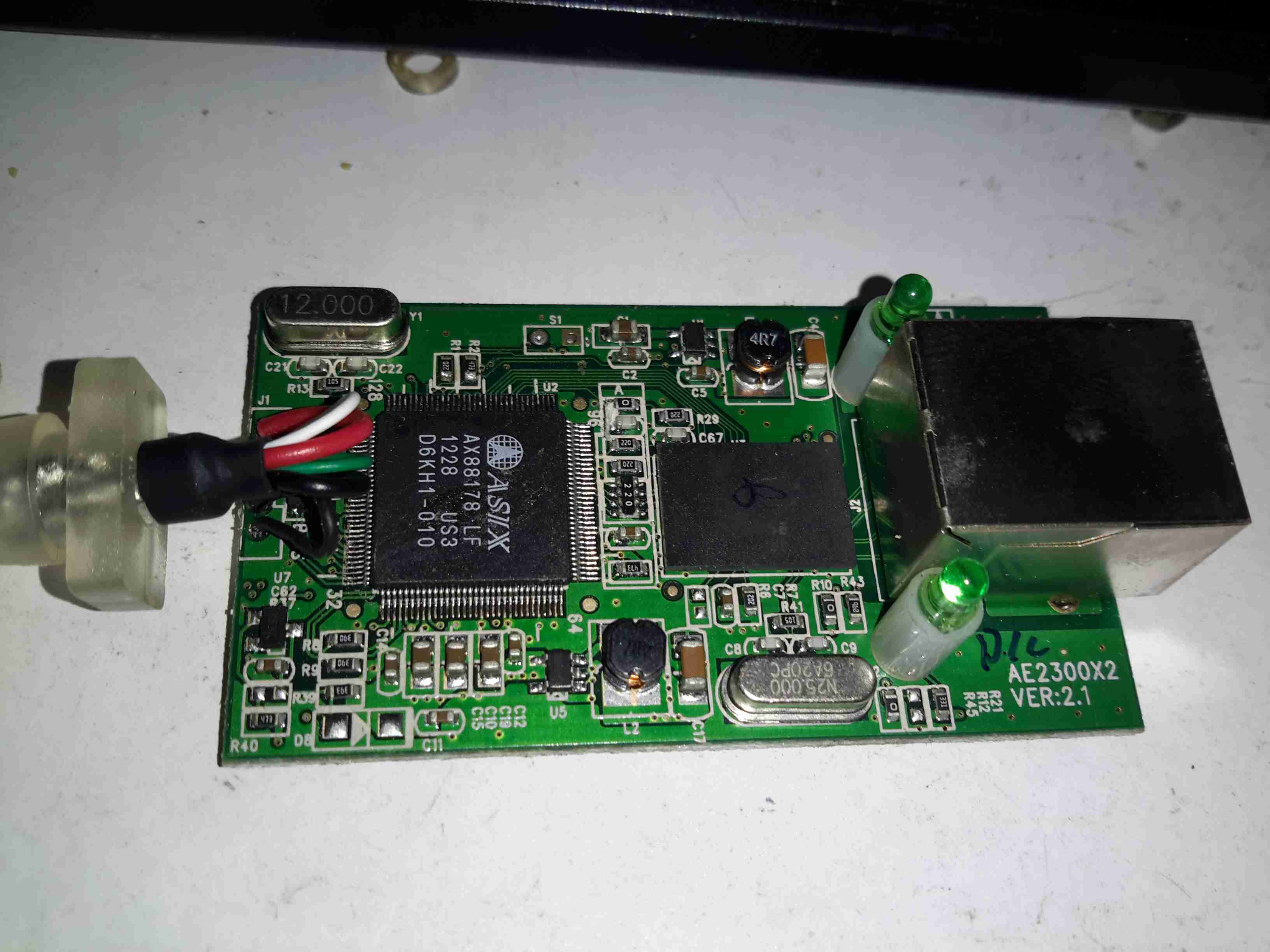
Here’s a chap eBay USB-To-Ethernet dongle I obtained for use with the Raspberry Pi Zero. This one is getting torn down permanently, as it’s rather unreliable. It seems to like having random fits where it’ll not enumerate on the USB bus. The silicon in the ICs will eventually make it here once I manage to get a new microscope 😉
Main Chipset
This is quite a heavily packed PCB, with the main Asix AX88178 on the left. This IC contains all of the logic for implementing the Ethernet link over USB, except the PHY. It’s clock crystal is in the top left corner.
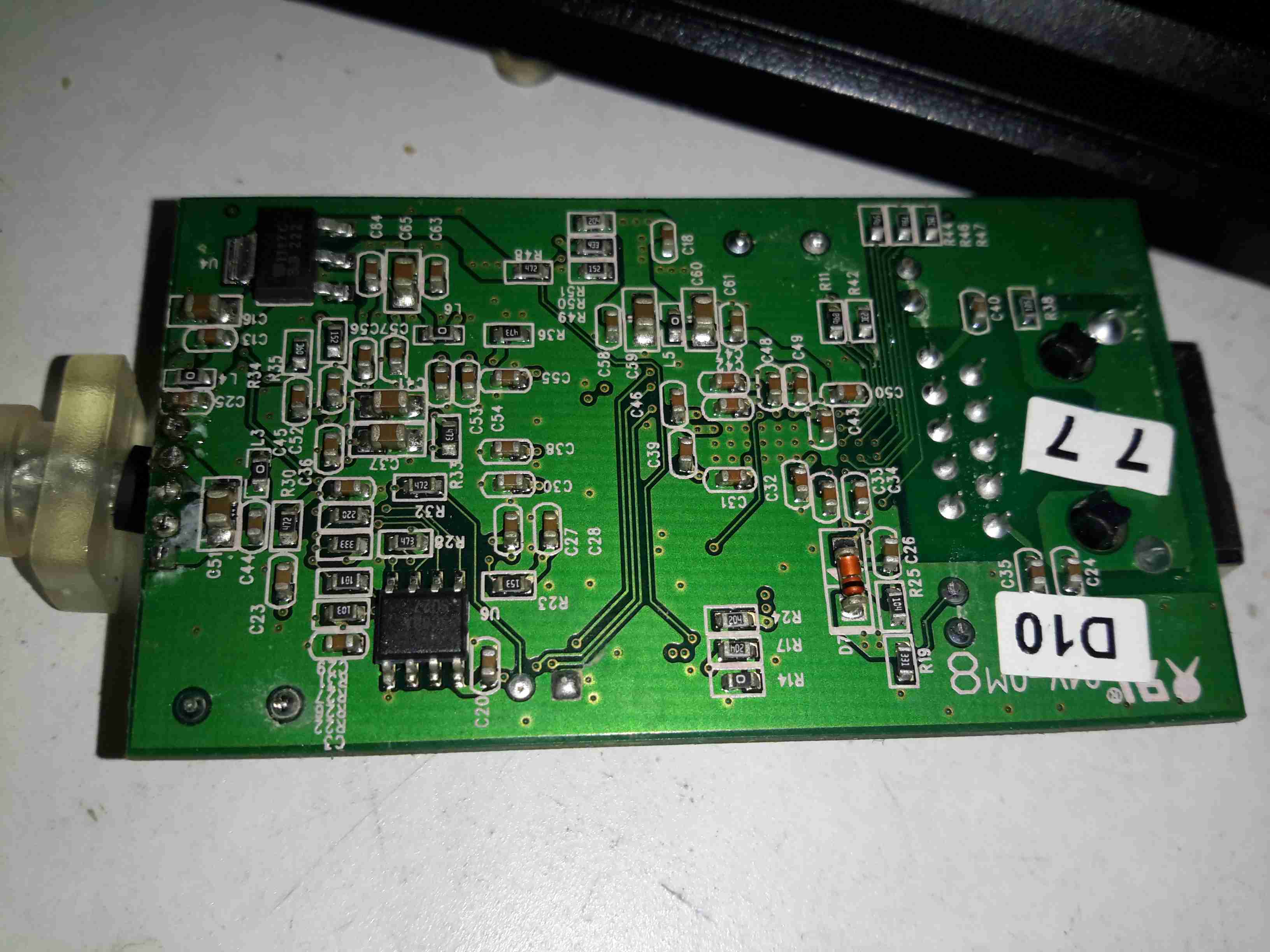
Reverse Side
Not much on the reverse side, there’s a 3.3v linear regulator at top left, the SOIC is an Atmel AT93C66A 4KB EEPROM for configuration data.
Vitesse PHY
The final IC in the chain is the Vitesse VSC8211 Gigabit PHY, with it’s clock crystal below. This interfaces the Ethernet MAC in the Asix IC to the magjack on the right.
This is a cheap little eBay reader to replace my ~10 year old multi-reader that very recently died. My original was an 8-in-1 version, but as I never read anything else other than SD cards these days, a little USB dongle version was more convenient.
Controller Chipset
The layout is very minimal, just the µSD socket, bypass passives & the main controller chip on this side, which is a GL3224 Dual LUN Memory Card Controller from Genesys Logic. This is fully USB3 capable according to the datasheet, but I’m not certain of the advantage of this for something that reads relatively slow devices like SD cards.
SD Socket
The other side of the PCB holds the full size SD socket, along with the activity LED & USB connector.
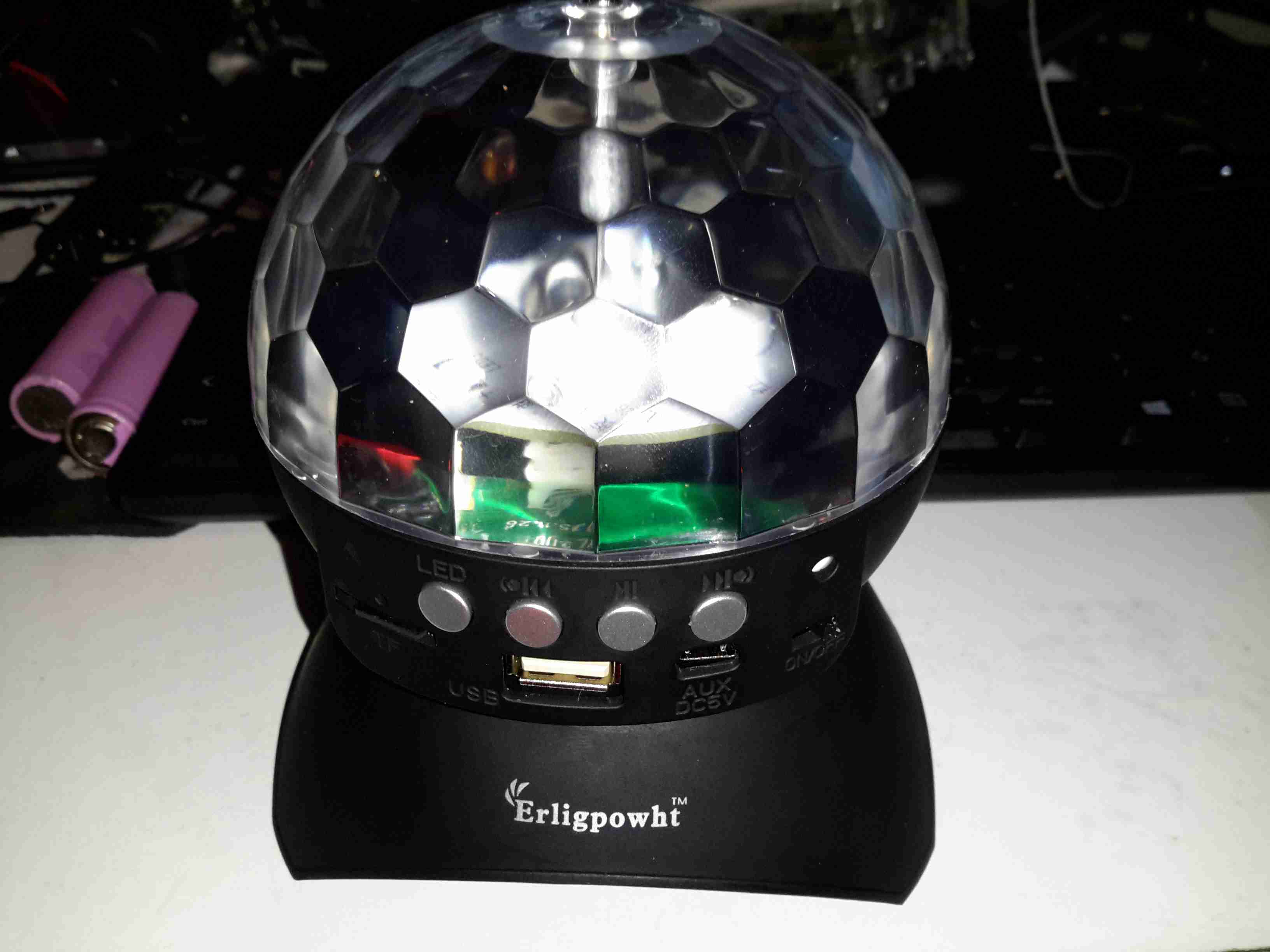
Here’s an eBay oddity – it’s got the same light & lens mechanism as the cheap “disco light” style bulbs on eBay, but this one is battery powered & has a built in MP3 player.
MP3 Disco Light
This device simply oozes cheapness. The large 4″ plastic dome lens sits on the top above the cheap plastic moulding as a base, which also contains the MP3 player speaker.
Controls
There are few controls on this player, the volume buttons are combined with the skip track buttons, a long press operates the volume control, while a short press skips the tracks. Several options for getting this thing to play music are provided:
Bluetooth – Allows connection from any device for bluetooth audio
USB – Plugging in a USB flash drive with MP3 files
SD Card – Very similar to the USB flash drive option, just a FAT32 formatted card with MP3 files
Aux – There’s no 3.5mm jack on this unit for an audio input, instead a “special” USB cable is supplied that is both used to charge the built in battery & feed an audio signal. This is possible since the data lines on the port aren’t used. But it’s certainly out of the ordinary.
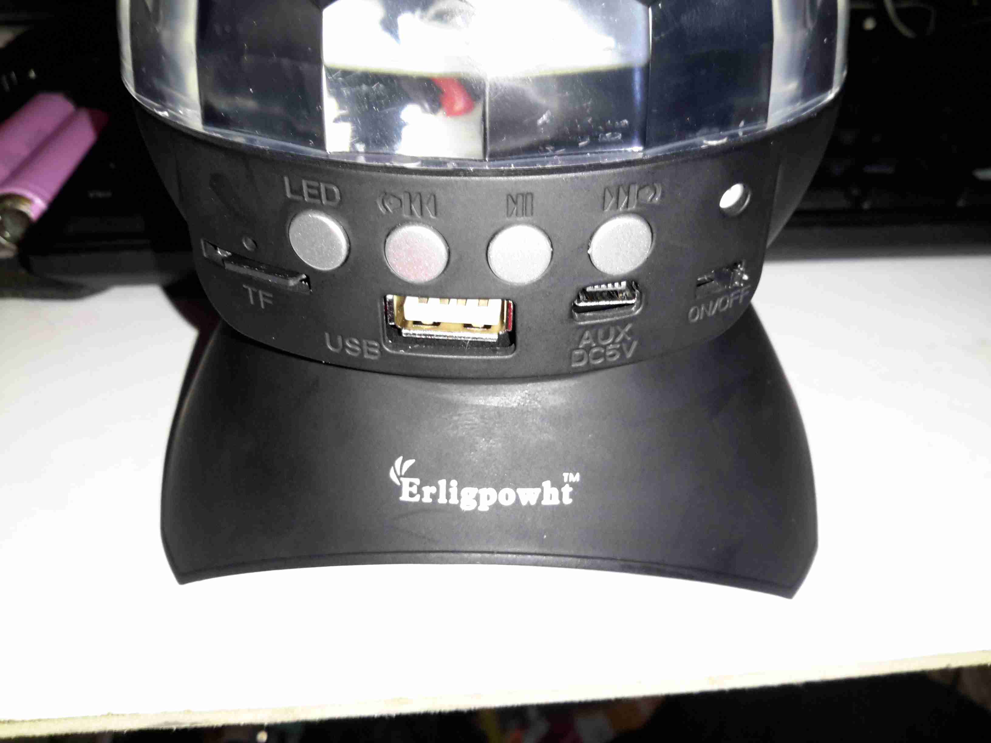
Top Removed
The top comes off with the removal of a single screw in the centre of the lens. The shaft in the centre that holds the lens is attached to a small gear motor under the LED PCB. There’s 6 LEDs on the board, to form an RGB array. Surprisingly for a very small battery powered unit these are bright to the point of being utterly offensive.
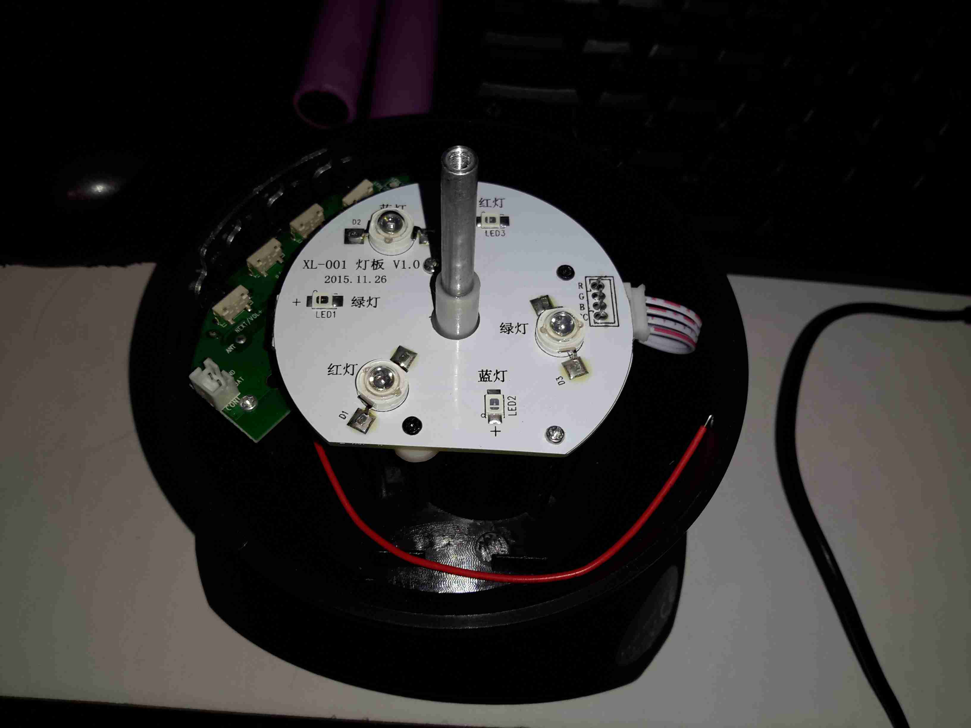
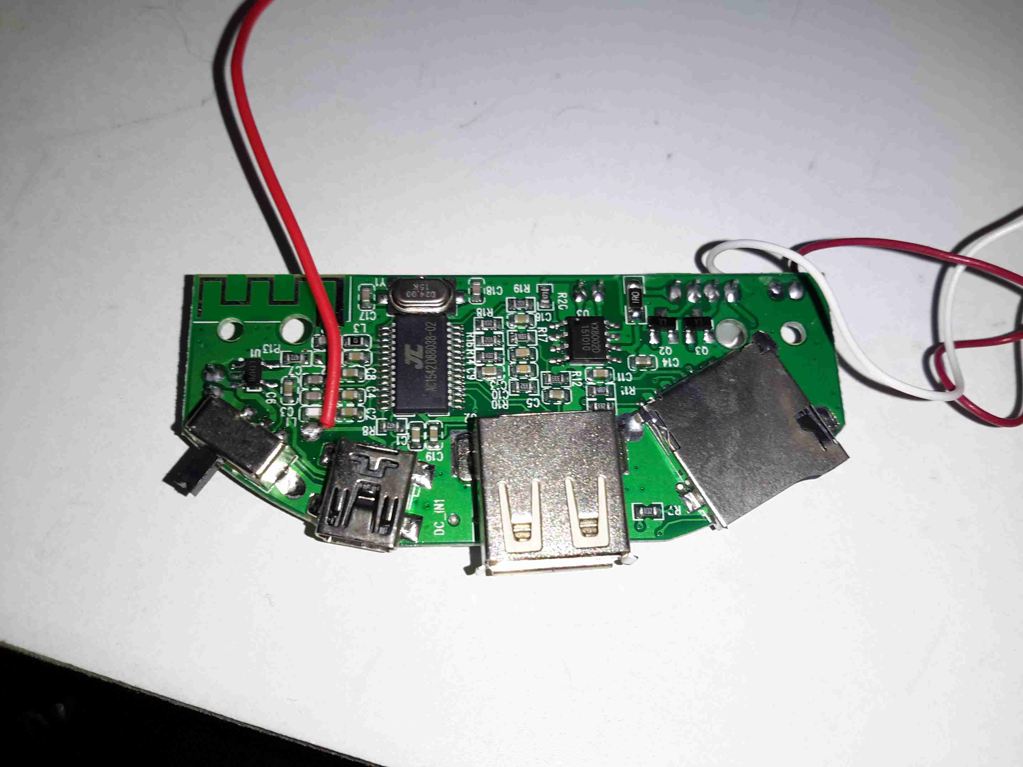
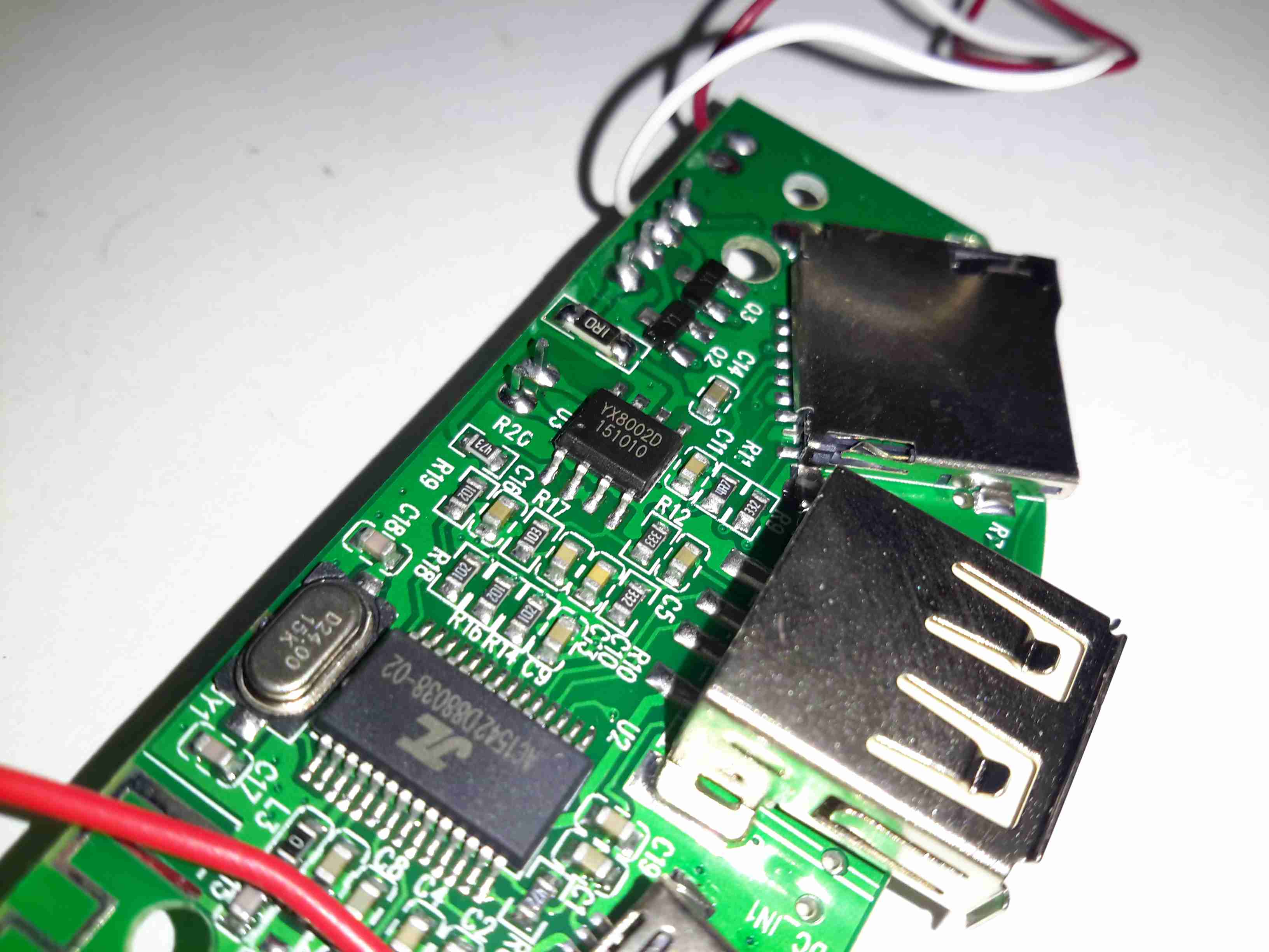
Mainboard
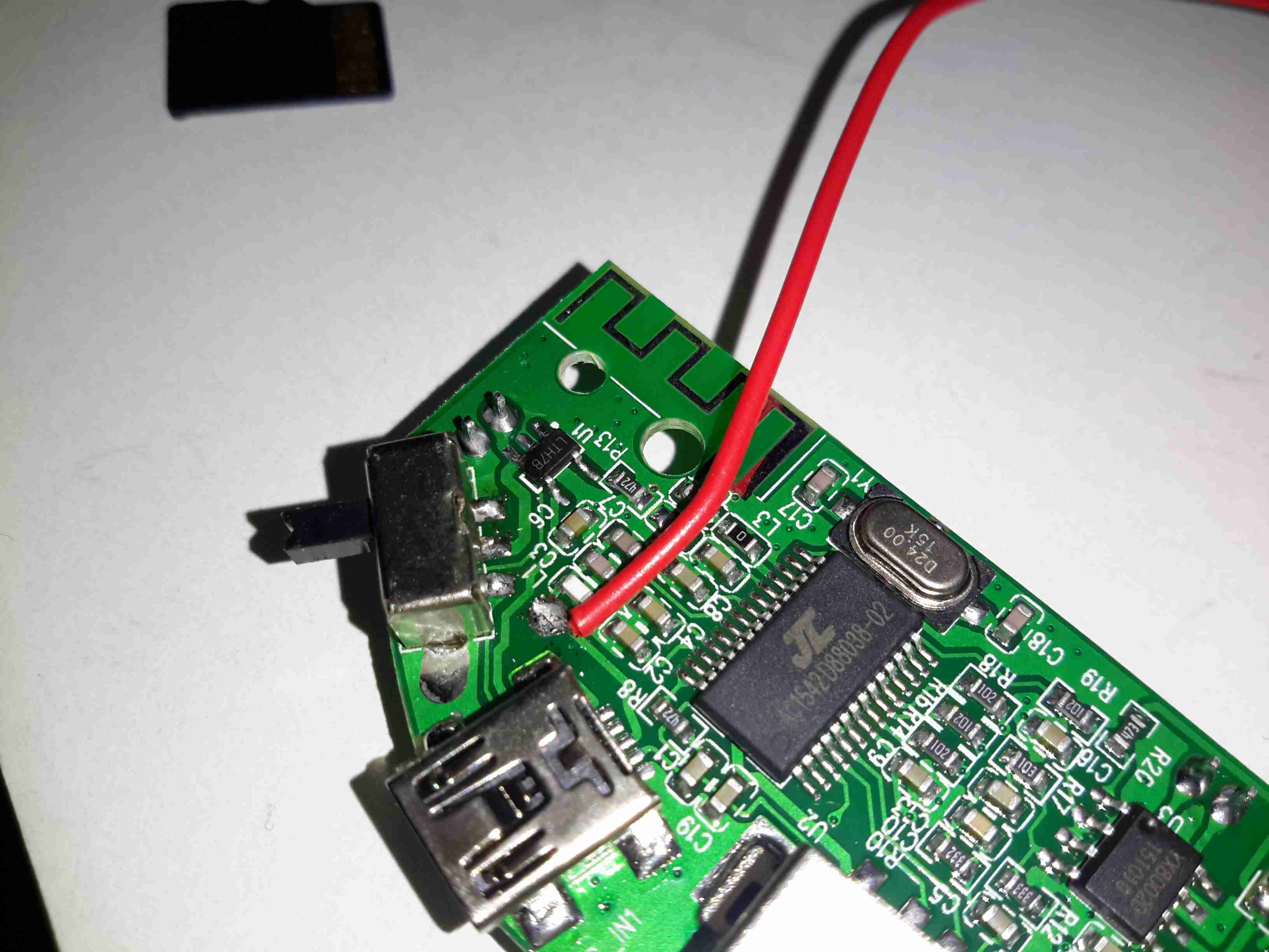
Here’s the mainboard removed from the plastic base. There’s not much to this device, even with all the options it has. The power switch is on the left, followed by the Mini-B USB charging port & aux audio input. The USB A port for a flash drive is next, finishing with the µSD slot. I’m not sure what the red wire is for on the left, it connects to one of the pins on the USB port & then goes nowhere.
Audio Amplifier
The audio amplifier is a YX8002D, I couldn’t find a datasheet for this, but it’s probably Class D.
Main Chipset
Finally there’s the main IC, which is an AC1542D88038. I’ve not been able to find any data on this part either, it’s either a dedicated MP3 player with Bluetooth radio built in, or an MCU of some kind.The RF antenna for the Bluetooth mode is at the top of the board.
Just behind the power switch is a SOT23-6 component, which should be the charger for the built in Lithium Ion cell.
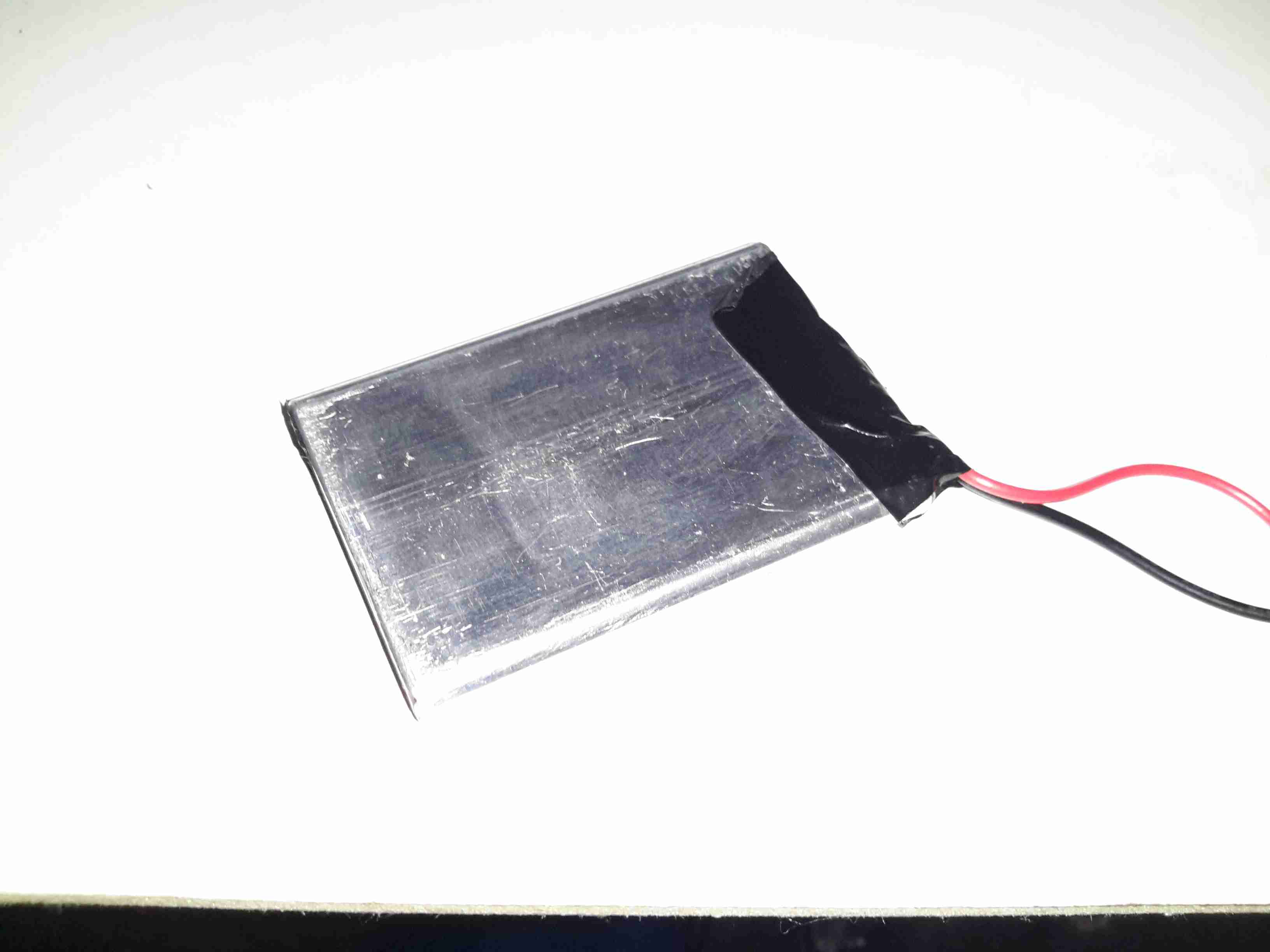
Lithium Ion Cell
The cell itself is a prismatic type rated in the instructions at 600mAh, however my 1C discharge test gave a reading of 820mAh, which is unusual for anything Li-Ion based that comes from eBay 😉
There is cell protection provided, it’s under the black tape on the end, nothing special here.
The main issue so far with this little player is the utterly abysmal battery life – at full volume playing MP3s from a SD card, the unit’s current draw is 600mA, with the seizure & blindness-inducing LEDs added on top, the draw goes up to about 1200mA. The built in charger is also not able to keep up with running the player while charging. This in all only gives a battery life of about 20 minutes, which really limits the usability of the player.
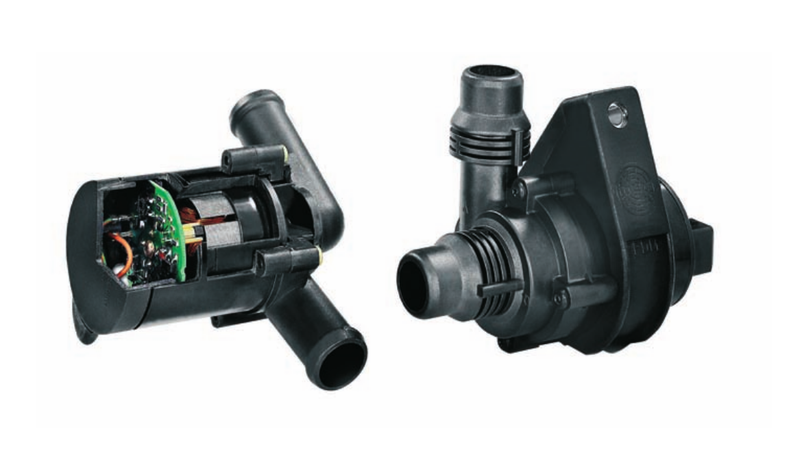
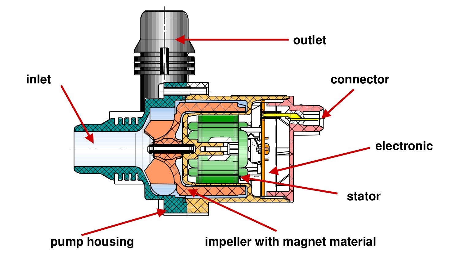
With some recent upgrades to the boat’s heating system, the hot water circulation pumps we’ve been using are becoming far too small for the job. After the original Johnson Marine circulation pump died of old age (the brushes wore down so far the springs ate the commutator) some time ago, it was replaced with a Pierburg WUP1 circulation pump from a BMW. (As we’re moored next to a BMW garage, these are easily obtainable & much cheaper than the marine pumps).
WUP1 Cutaway
These are also brushless, where as the standard Johnson ones are brushed PM motors – the result here is a much longer working life, due to fewer moving parts.
The rated flow & pressure on these pumps is pretty pathetic, at 13L/min at 0.1bar head pressure. As the boat’s heating system is plumbed in 15mm pipe instead of 22mm this low pressure doesn’t translate to a decent flow rate. Turns out it’s pretty difficult to shove lots of water through ~110ft of 15mm pipe ;). Oddly enough, the very low flow rate of the system was never a problem for the “high output” back boiler on the stove – I suspect the “high output” specification is a bit optimistic.
This issue was recently made worse with the addition of a Webasto Thermo Top C 5kW diesel-fired water heater, which does have it’s own circulation pump but the system flow rate was still far too low to allow the heater to operate properly. The result was a rapidly cycling heater as it couldn’t dump the generated hot water into the rest of the system fast enough.
The easiest solution to the problem here is a larger pump with a higher head pressure capability. (The more difficult route would be completely re-piping the system in 22mm to lower the flow resistance). Luckily Pierburg produce a few pumps in the range that would fit the job.
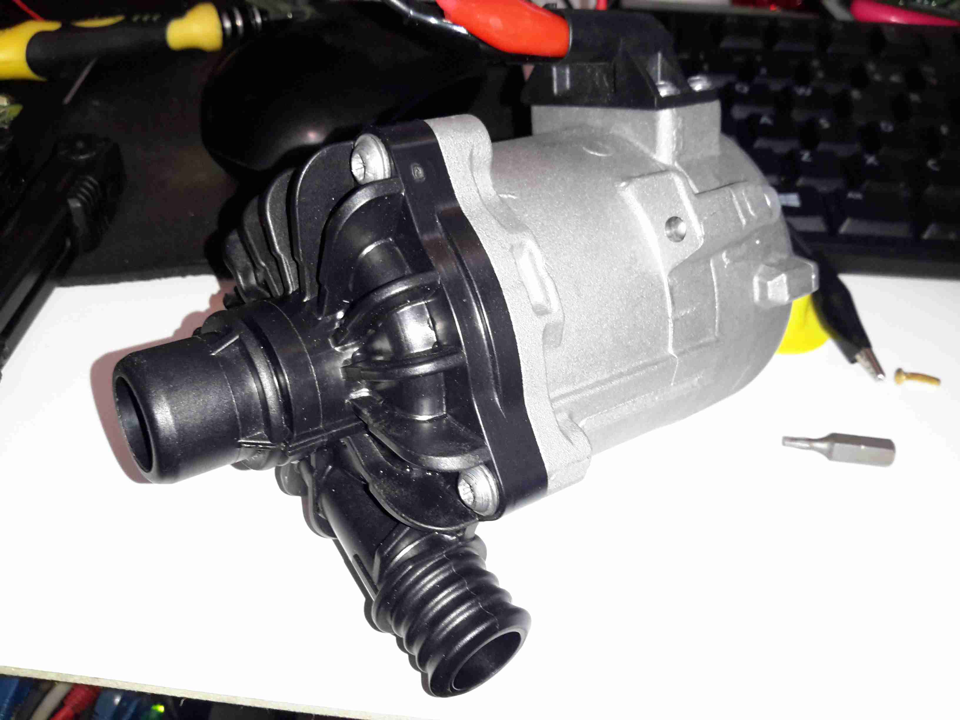
Pierburg CWA-50
Here’s the next size up from the original WUP1 pump, the CWA50. These are rated at a much more sensible 25L/min at 0.6bar head pressure. It’s physically a bit larger, but the connector sizes are the same, which makes the install onto the existing hoses easier. (For those that are interested, the hose connectors used on BMW vehicles for the cooling system components are NormaQuick PS3 type. These snap into place with an O-Ring & are retained by a spring clip).
The CWA50 draws considerably more power than the WUP1 (4.5A vs 1.5A), and are controllable with a PWM signal on the connector, but I haven’t used this feature. The PWM pin is simply tied to the positive supply to keep the pump running at maximum speed.
Once this pump was installed the head pressure immediately increased on the gauge from the 1 bar static pressure to 1.5 bar, indicating the pump is running at about it’s highest efficiency point. The higher water flow has so far kept the Webasto happy, there will be more to come with further improvements!
CWA-50 Pump Teardown
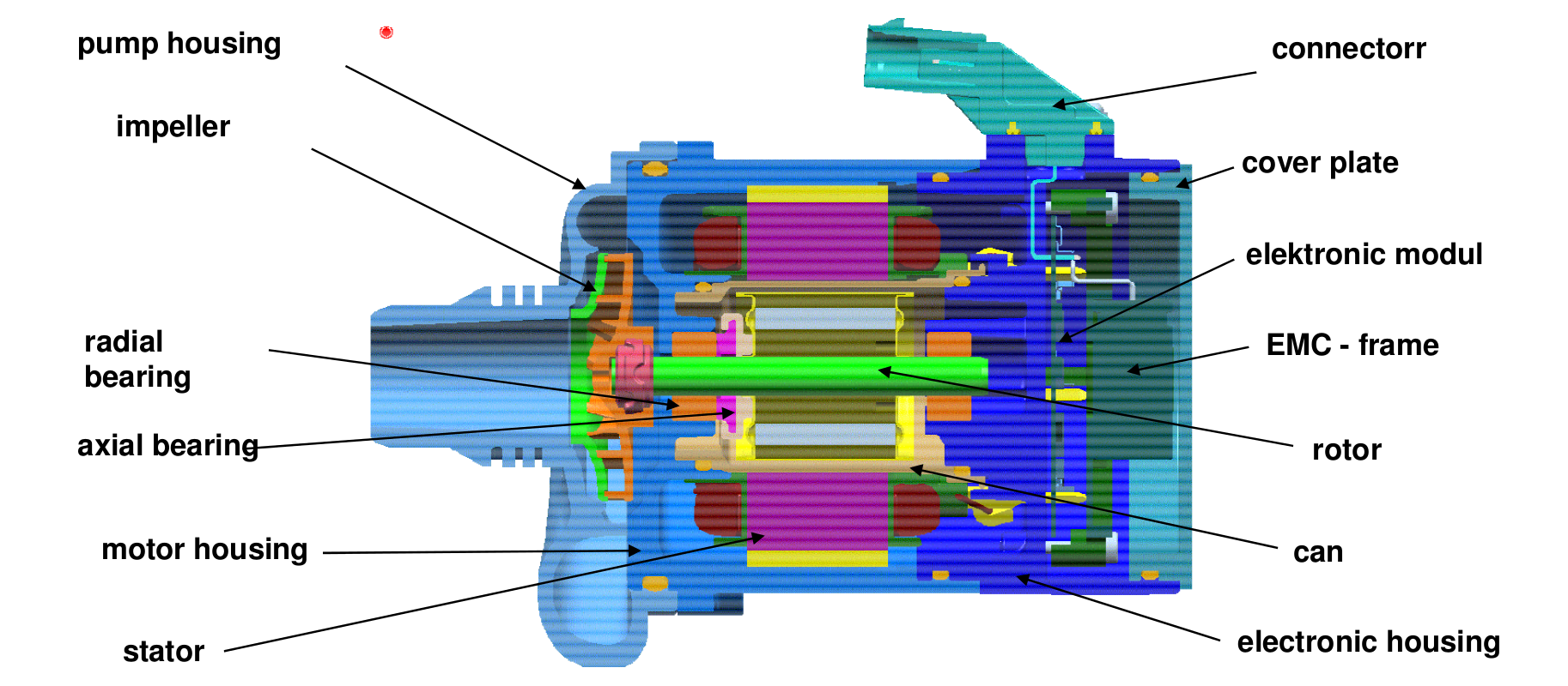
CWA50 Cutaway
Above is a cutaway drawing of the new pump. These have a drilling through the shaft allows water to pass from the high pressure outlet fitting, through the internals of the pump & returns through the shaft to the inlet. This keeps the bearings cool & lubricated. The control & power drive circuitry for the 3-phase brushless motor is attached to the back & uses the water flowing through the rotor chamber as a heatsink. Overall these are very well made pumps.
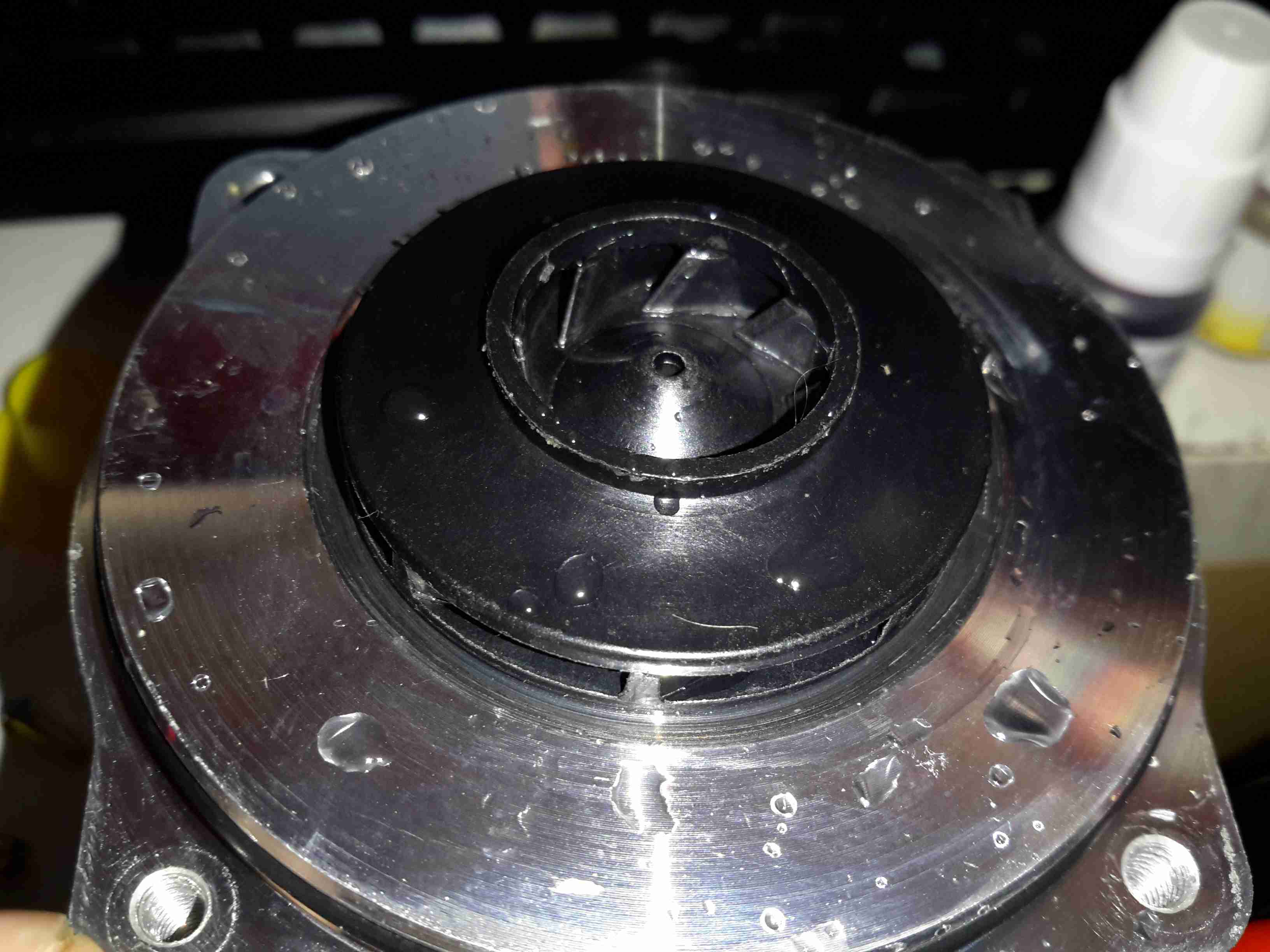
Impeller
Here’s the impeller of the pump, which is very small considering the amount of power this unit has. The return port for the lubricating water can be seen in the centre of the impeller face.
3-Phase Driver
Inside the back of the pump is the control module. The main microcontroller is hiding under the plastic frame which holds the large power chokes & the main filter electrolytic.
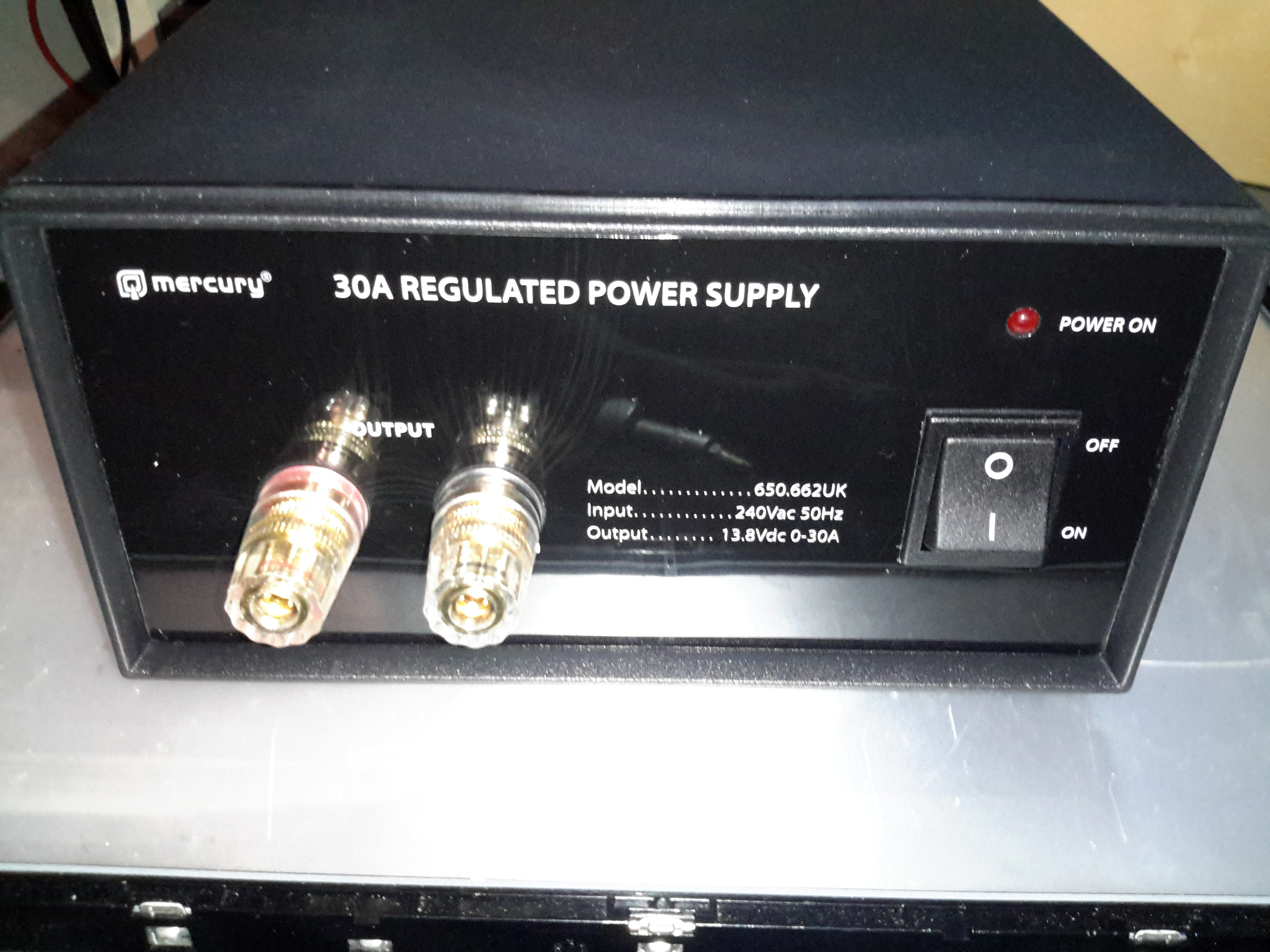
After having a couple of the cheap Chinese PSUs fail on me in a rather spectacular fashion, I decided to splash on a more expensive name-brand PSU, since constantly replacing PSUs at £15 a piece is going to get old pretty fast. This is the 30A model from Mercury, which seems to be pretty well built. It’s also significantly more expensive at £80. Power output is via the beefy binding posts on the front panel. There isn’t any metering on board, this is something I’ll probably change once I’ve ascertained it’s reliability. This is also a fixed voltage supply, at 13.8v.
Rear Panel
Not much on the rear panel, just the fuse & cooling fan. This isn’t temperature controlled, but it’s not loud. No IEC power socket here, the mains cable is hard wired.
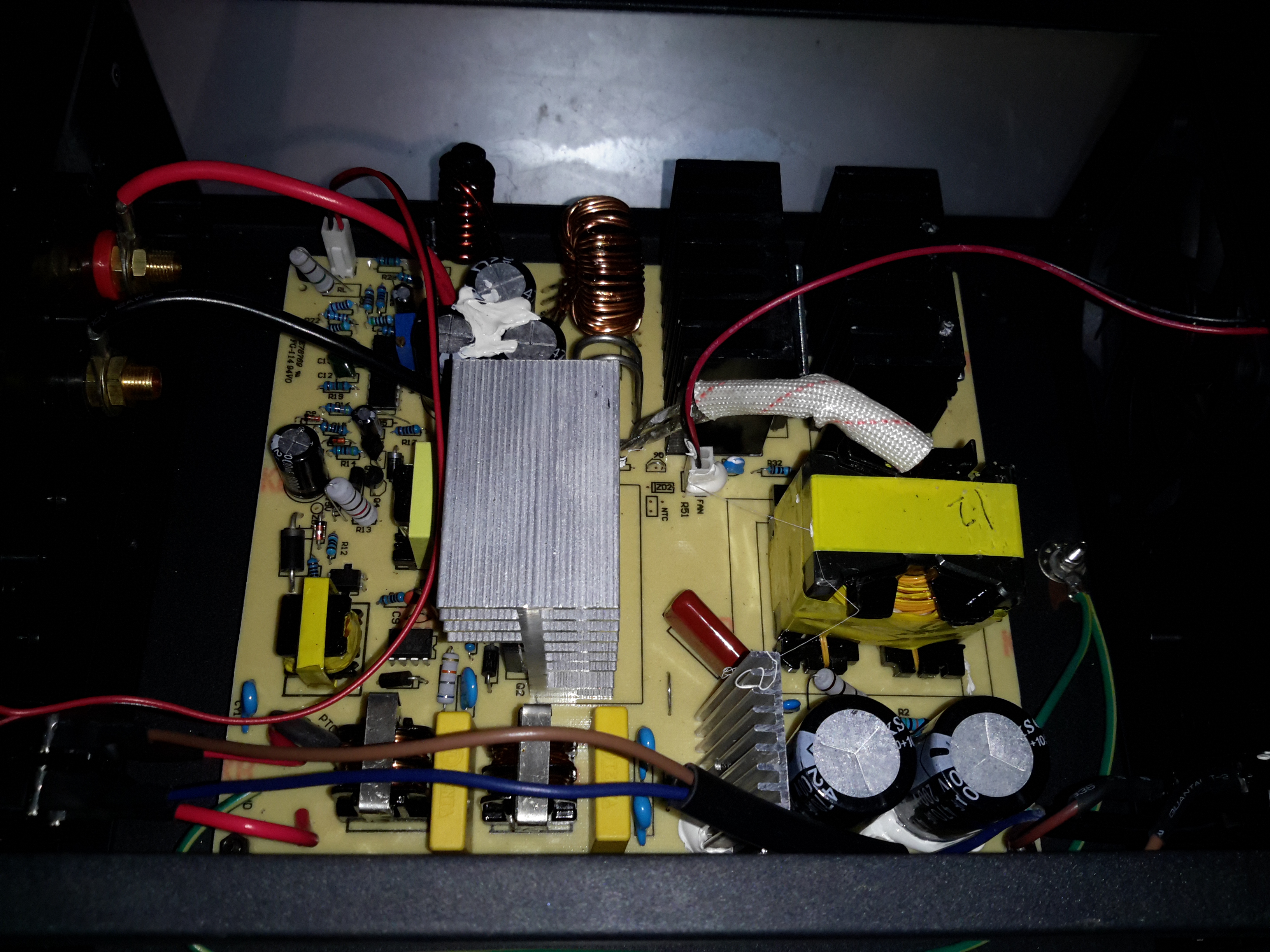
Main Board
Removing some spanner-type security screws reveals the power supply board itself. Everything on here is enormous to handle the 30A output current at 13.8v. The main primary side switching transistors are on the large silver heatsink in the centre of the board, feeding the huge ferrite transformer on the right.
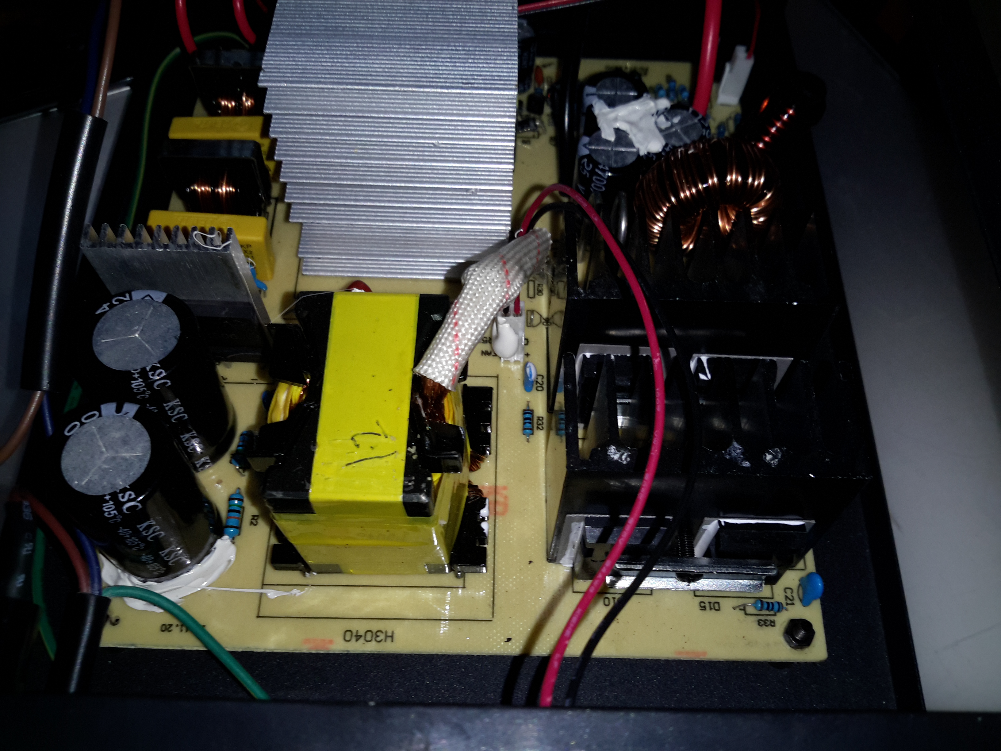
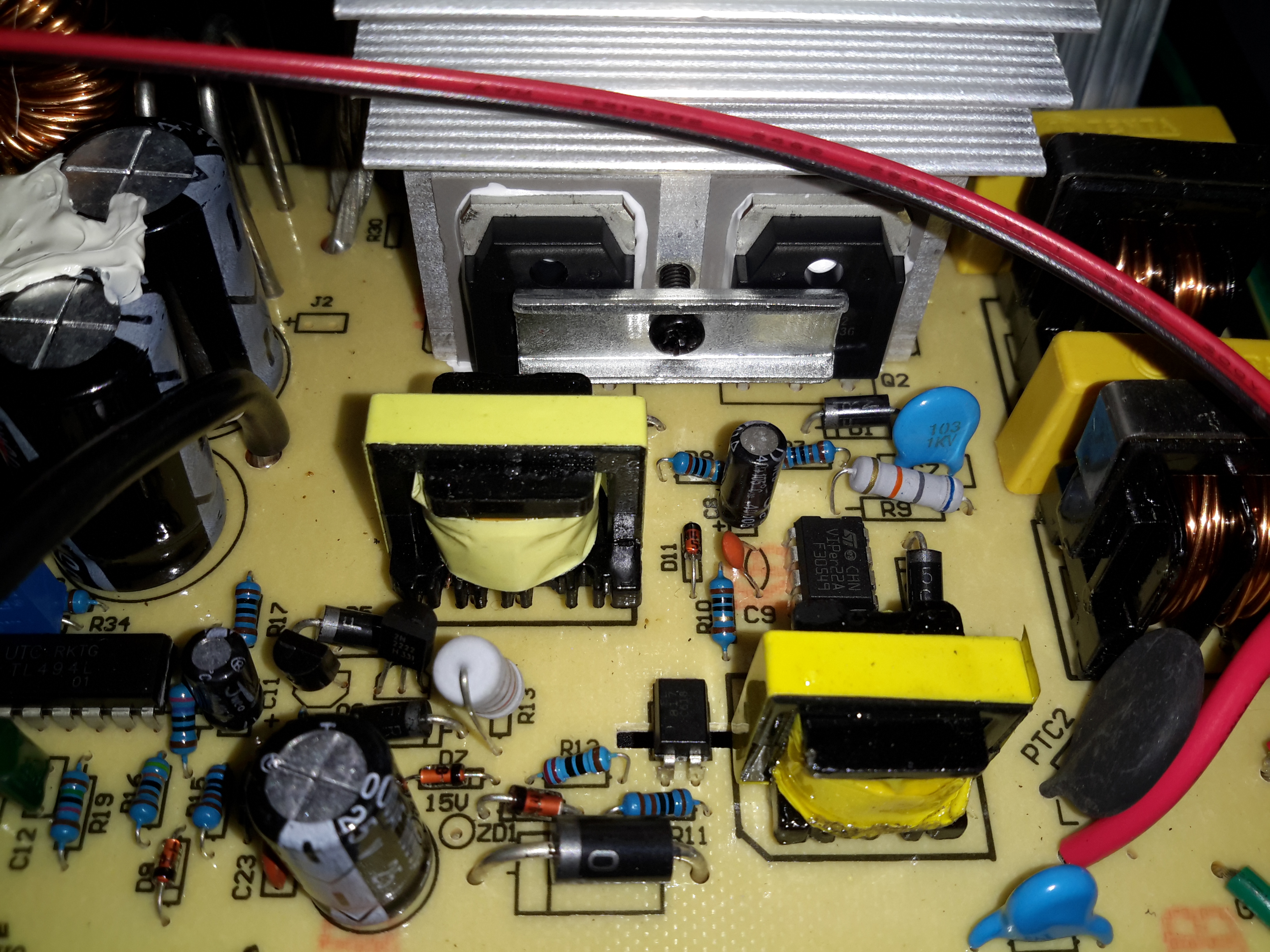
Transformer
The transformer’s low voltage output tap comes straight out instead of being on pins, due to the size of the winding cores. Four massive diodes are mounted on the black heatsinks for output rectification.
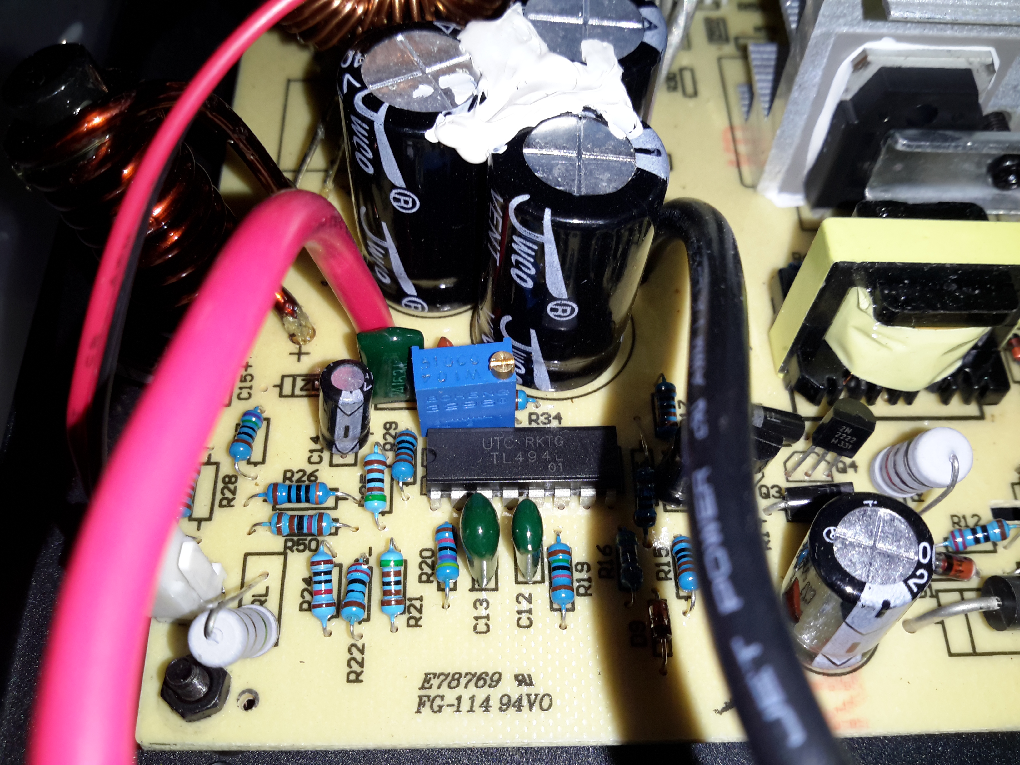
SMPS Controller
The supply is controlled via the jelly bean TL494 PWM controller IC. The multi-turn potentiometer doesn’t adjust the output voltage, more likely it adjusts the current limit.
Standby Supply
Power to initially start the supply is provided by a small SMPS circuit, with a VIPer22A Low Power Primary Switcher & small transformer on the lower right. The transformer upper left is the base drive transformer for the main high power supply.
In a word, no they aren’t any good. As usual, cheap doesn’t equal good, and in this case the cheapo clones are a total waste of money. Read on for the details!
I’ve been looking into using a cheap Chinese clone Honda GX35 engine to drive an automotive alternator as a portable battery charging & power unit. These engines are available very cheaply on eBay, aimed at the mini-bike/go-kart market.
For those not in the know, the Honda GX25/35 4-strokes are strimmer-type engines that traditionally were always of 2-stroke construction. Honda worked out how to have a wet-sump engine without the need to keep the engine always in the “upright” position. They do not require mixing of oil into the fuel for lubrication as 2-strokes do, so should be much cleaner running.
So far I’ve had two of these cheap engines, as the first one died after only 4 hours run time, having entirely lost compression. At the time the engine was idling, no load, having been started from cold only a few minutes before. Having checked the valve clearances to make sure a valve wasn’t being held partially open, I deduced that the cause was broken piston rings. This engine was replaced by the seller, so I didn’t get a chance to pull it to bits to find out, but I decided to do a full teardown on the replacement to see where the cloners have cut corners.
Oil Return Hose
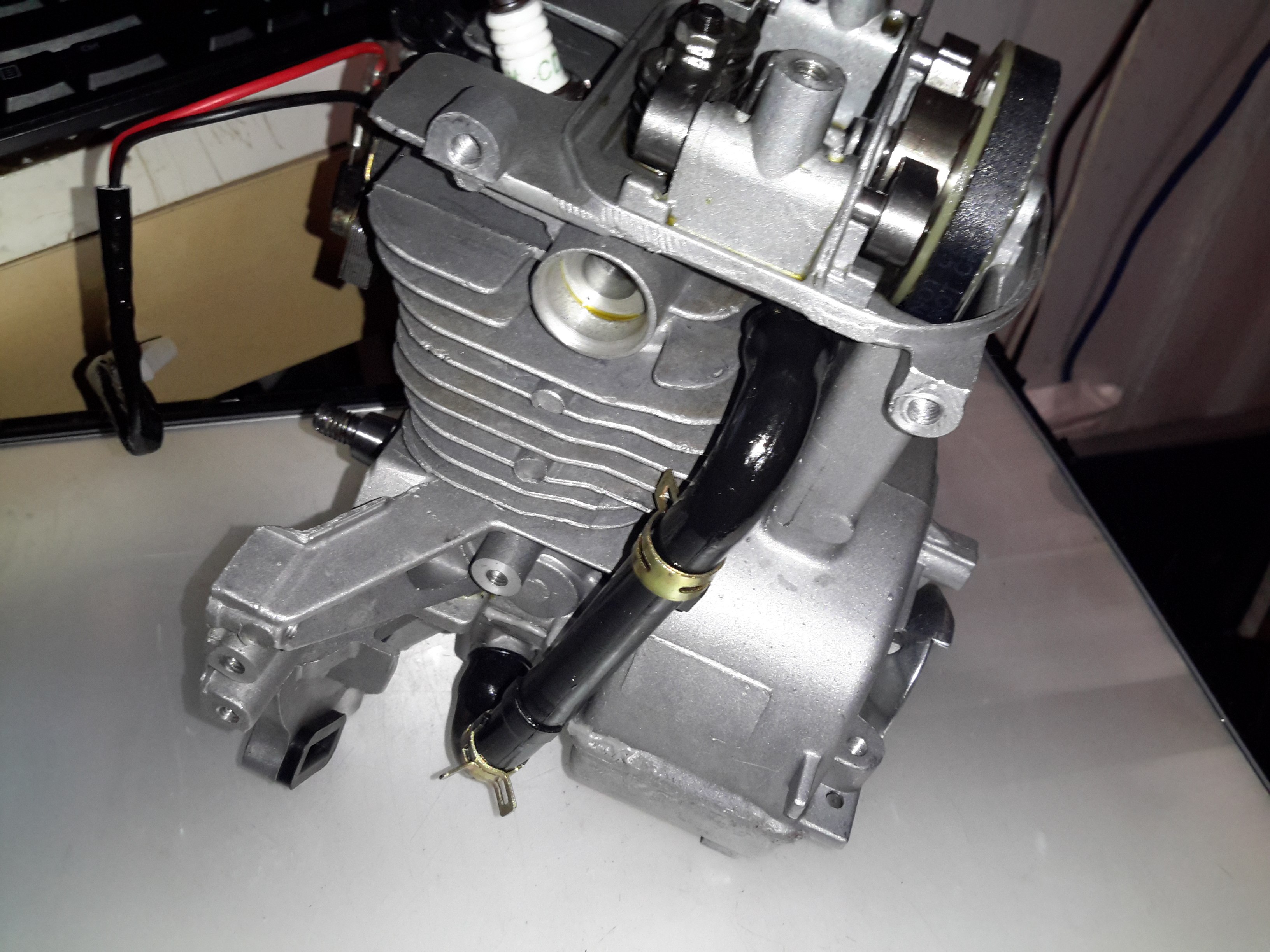
I’ve already stripped off the ancillary components: exhaust, carburettor, fuel tank, cowlings, as these parts are standard to any strimmer engine. The large black hose here is the oil return feed back to the rocker cover from the crankcase. The oiling system in these engines is rather clever. The main engine block is made of light alloy, probably some permutation of Aluminium. There is much flashing left behind between the cylinder fins from the die-casting process, and not a single engine manufacturer’s logo anywhere. (From what I’ve read, the genuine Honda ones have their logo on the side of the crankcase).
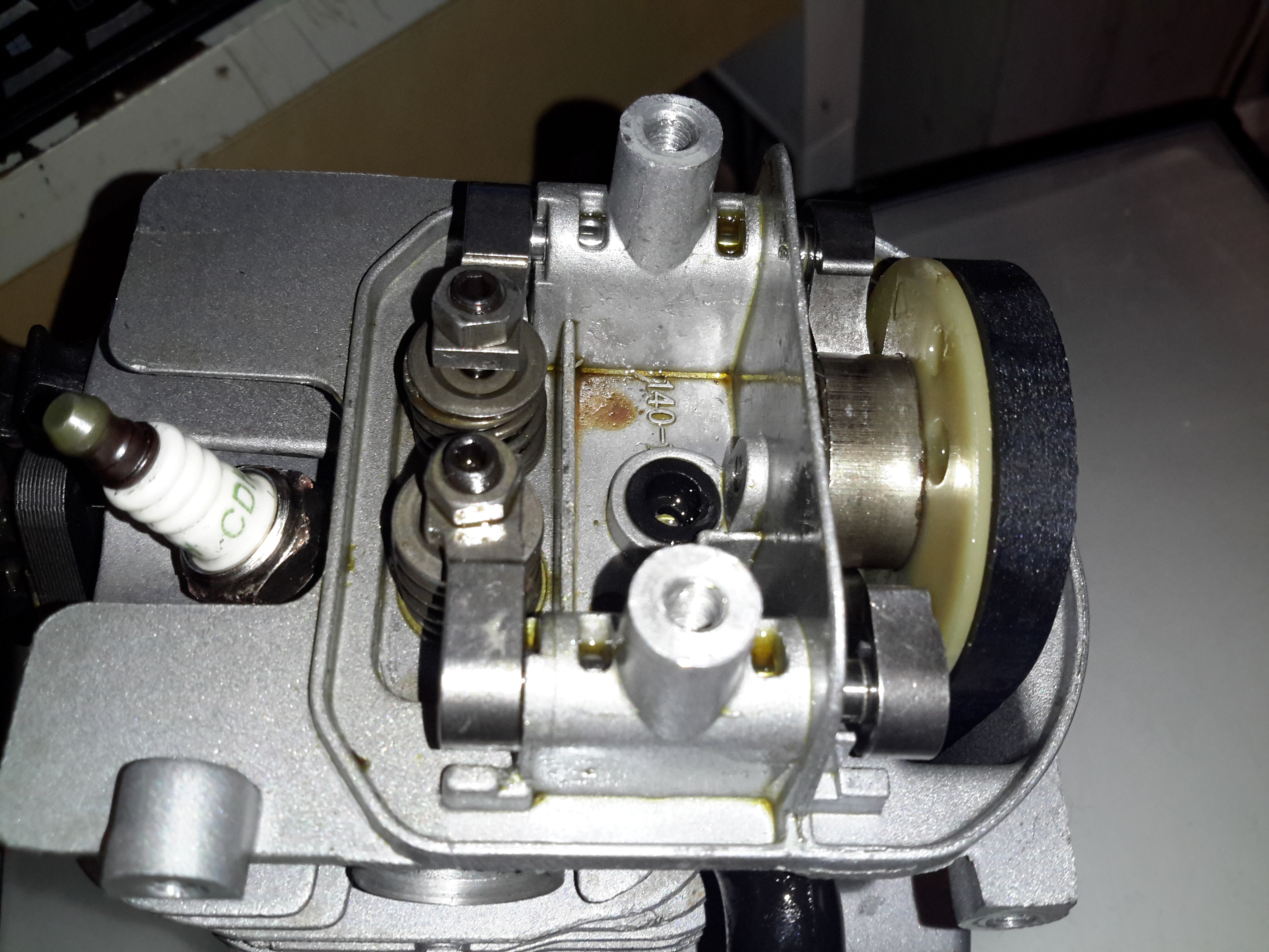
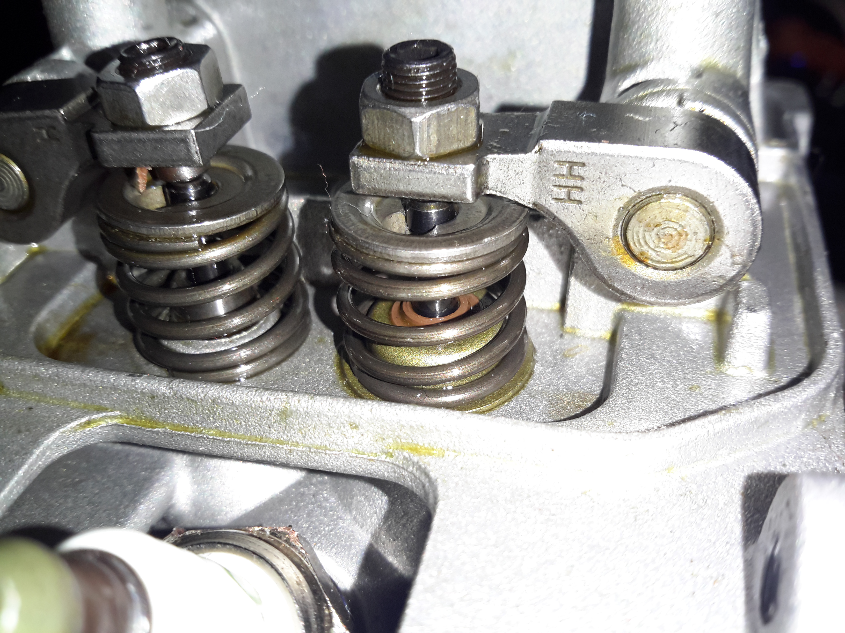
Rocker Box
Here’s the top of the engine with valves, rockers & camshaft. All the valve gear up here, minus the valves themselves & springs, are manufactured from sintered steel, there are no proper “bearings”, the steel shafts just run in the aluminium castings. The cam gear is of plastic, with the sintered steel cam pressed into place. The cam also has the bearing surface for the pin that the whole assembly rotates on. The timing belt runs in the oil & is supposed to last the life of the engine, and while I’d believe that in the original Honda, I certainly wouldn’t in this engine. The black grommet is the opening of the oil return gallery.
Cam
Here’s the cam on the back of the plastic pulley. A single cam is used for both intake & exhaust valves for space & simplicity.
Intake Valve Stem Seal
Just visible under the intake valve spring is a simple stem seal, to hopefully prevent oil being sucked down the valve guide into the cylinder by intake vacuum. Running these cheap engines proves this seal to be ineffective, as they blow about as much blue oil smoke as a 2-stroke when they’re started cold. 😉
Starter Side
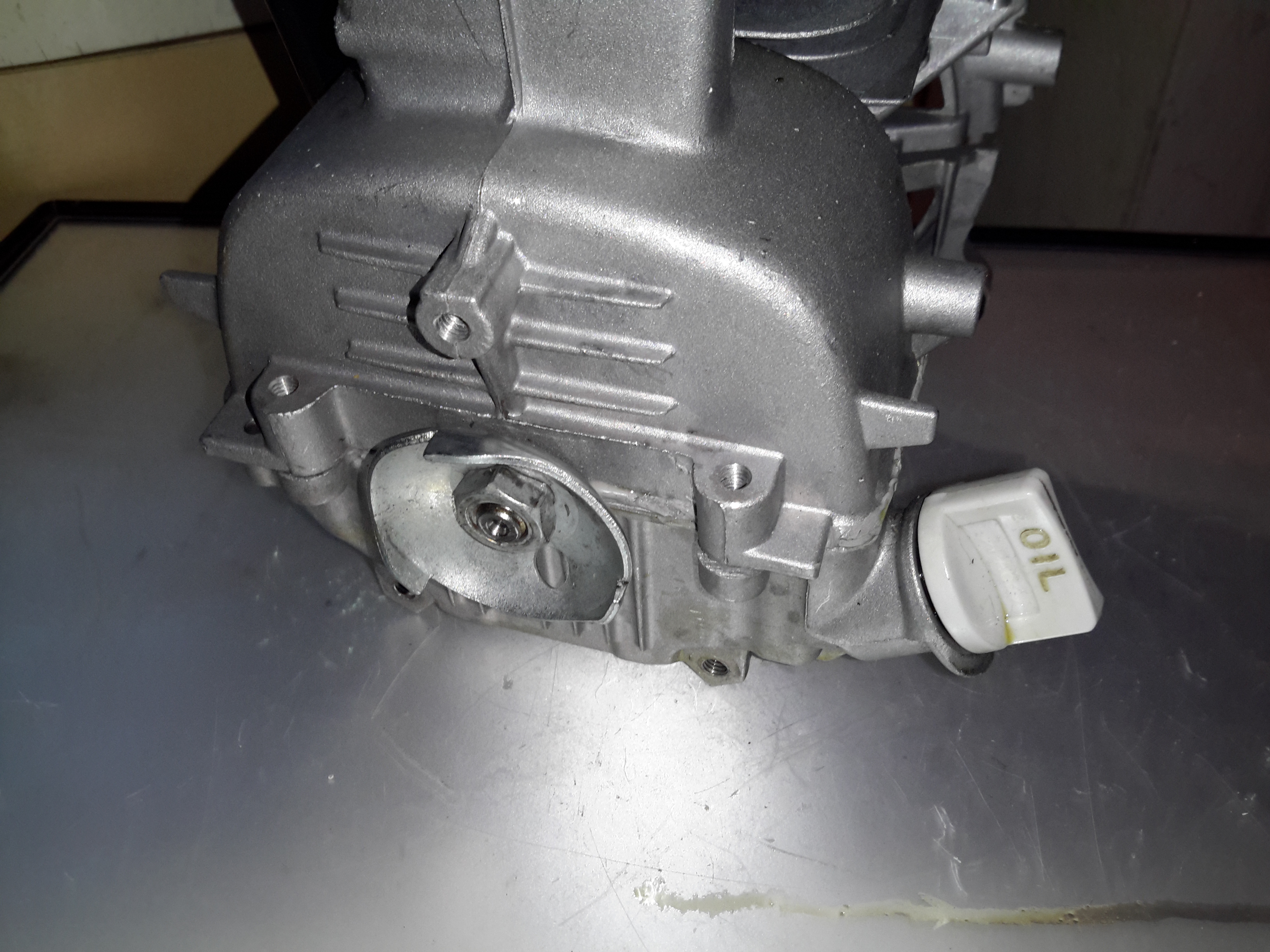
The starter side is where the oil sump is located on these engines, along with the dipstick.
Flywheel Side
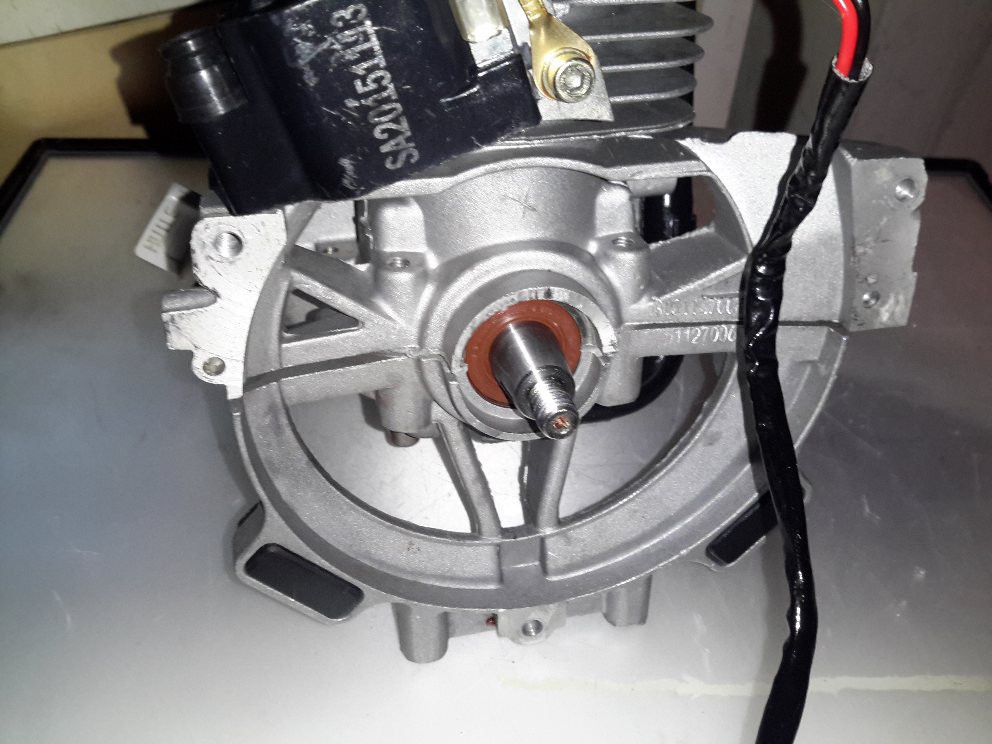
The flywheel end of the engine is the usual fare for small engines. Ignition is provided by a magneto, with a magnet in the flywheel. This is no different from the 2-stroke versions. As these ignitions fire on every revolution of the crankshaft, the spark plug fires both on compression, igniting the fuel for normal operation, and again into the exhaust stroke, where the spark is wasted.
One thing I have noticed about these engines is an almost total lack of cooling air coming through the cowling over the cylinder cooling fins. Plenty was flowing over the exhaust silencer side, I believe bad housing design would be what causes this problem. A lack of cooling certainly wouldn’t help engine longevity!
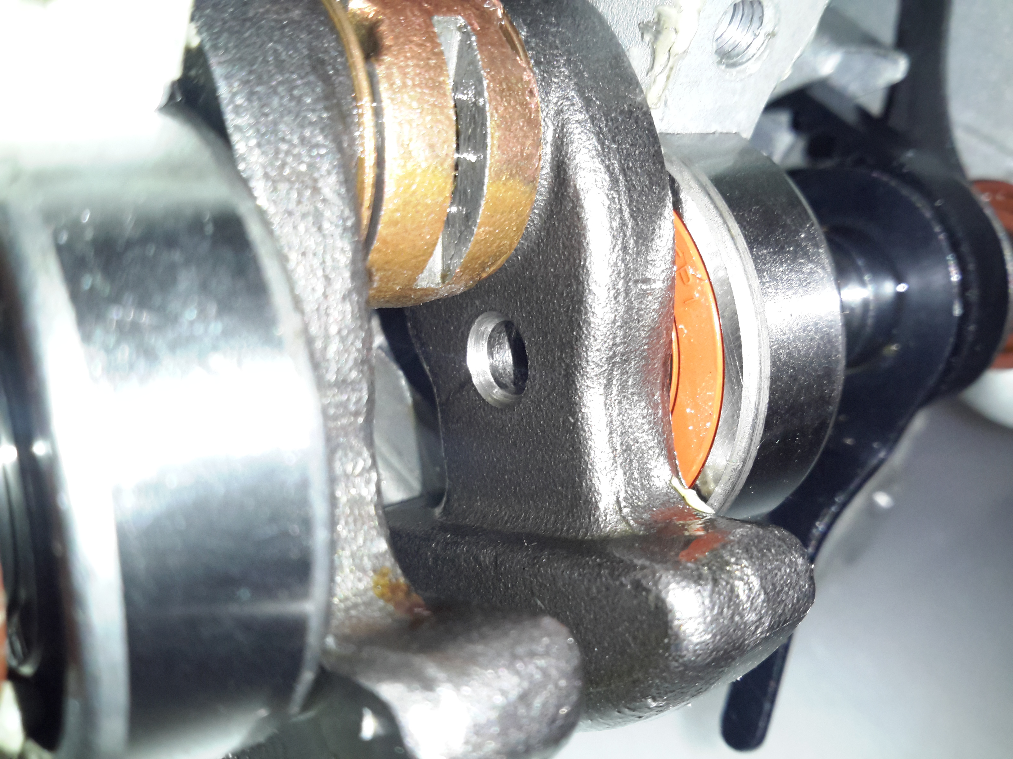
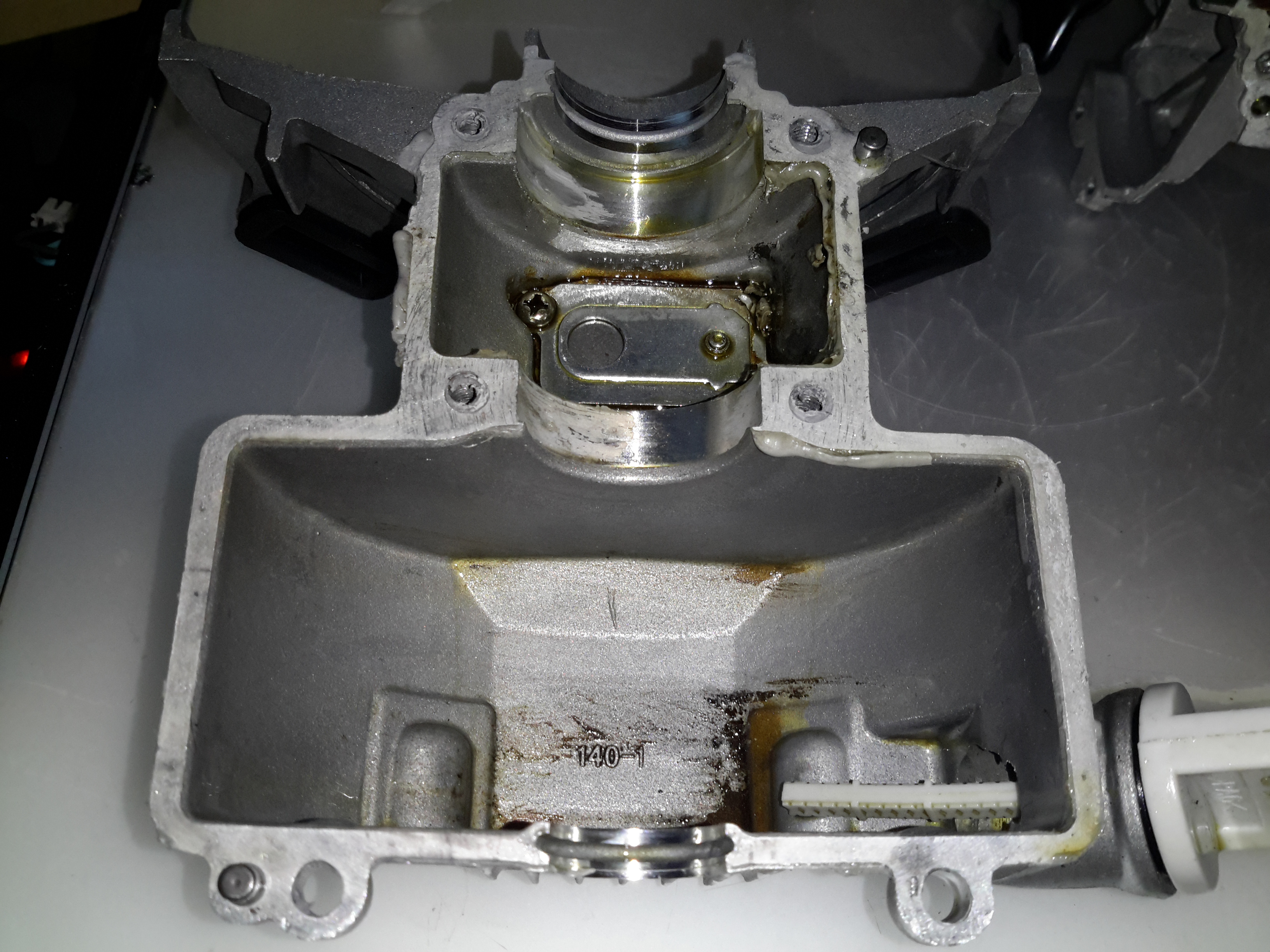
Engine “Sump”
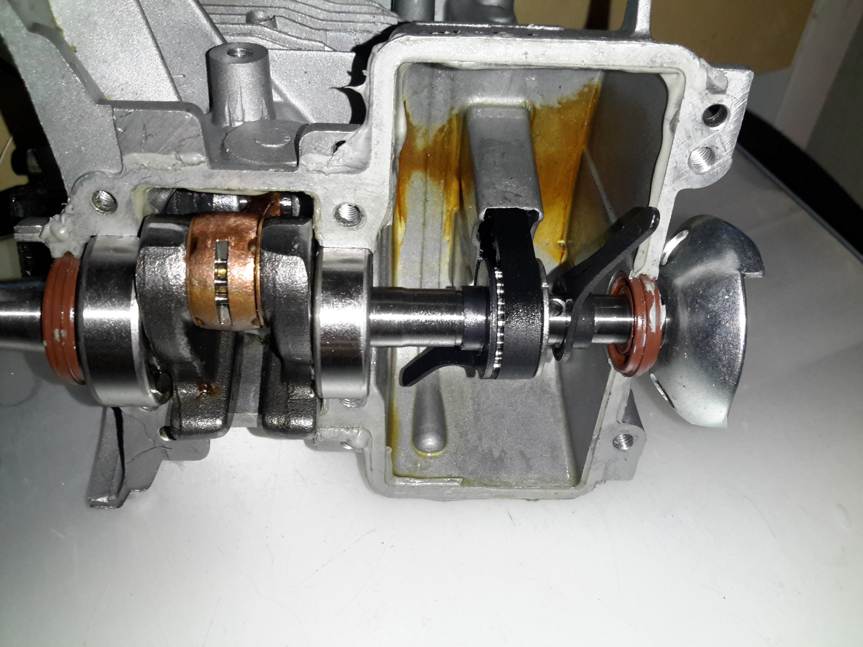
Separating the bottom of the engine was a little difficult, as there is a significant bead of sealant used instead of a gasket. Inside the sump of the engine are a pair of paddles, which stir up the oil into a mist. As the piston moves in the cylinder, it acts as a pump, creating alternating pulses of pressure & vacuum in the crankcase. Oil mist flows through a drilling in the crank from the sump, into the crankcase where it (hopefully) lubricates the bearings & the cylinder wall. Incidentally, the only main bearings are on the crankcase – the far end of the shaft that carries the oil paddles & timing belt is just flapping in the breeze, the only support being the oil seal in the outer housing. The crank itself isn’t hardened – a file easily removes metal from all parts that I could get at. The big end journal pin might be, but these cranks are pressed together so I can’t access that part.
Lubrication Gallery
The oil mist feeds into the crankcase through this hollow section of shaft, there’s a drilling next to the timing belt pulley to connect the two spaces together.
Lower Crankcase
The lower crankcase is just a simple die casting, there’s a check valve at the bottom under the crankshaft to transfer oil to the rocker cover, through the rubber tube on the outside of the engine. After the oil reaches the rocker box, it condenses & returns to the sump via the timing belt cavity.
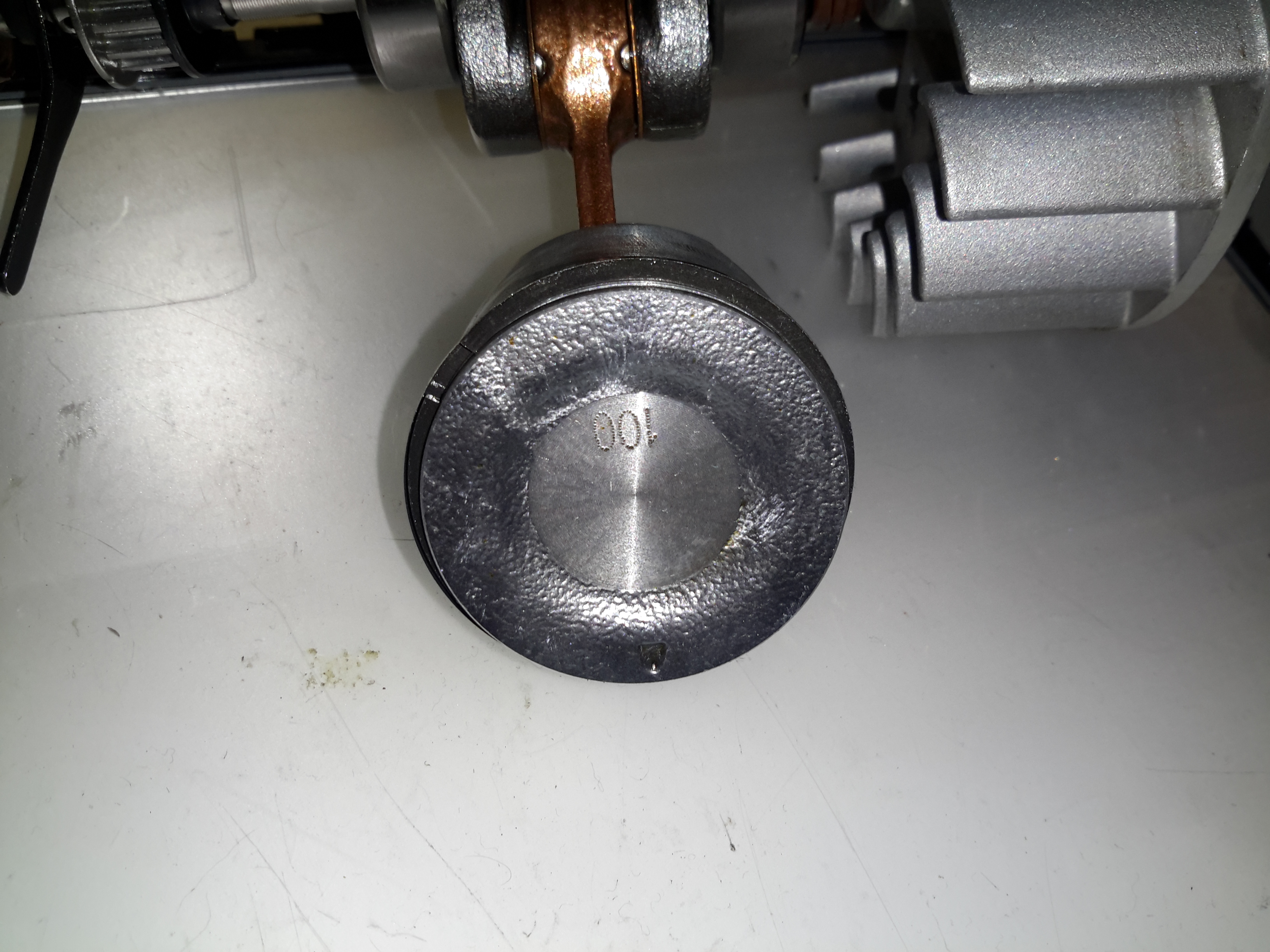
Piston Crown
Removing the crankshaft from the engine block gives me a look at the piston. The factory couldn’t even be arsed to machine the crown, it’s still got the rough finish from the hot-forging press. This bad finish will pick up much carbon from combustion, and would probably cause detonation once enough had accumulated to become incandescent in the heat of combustion. Only the centre is machined, just enough for them to stamp a number on.
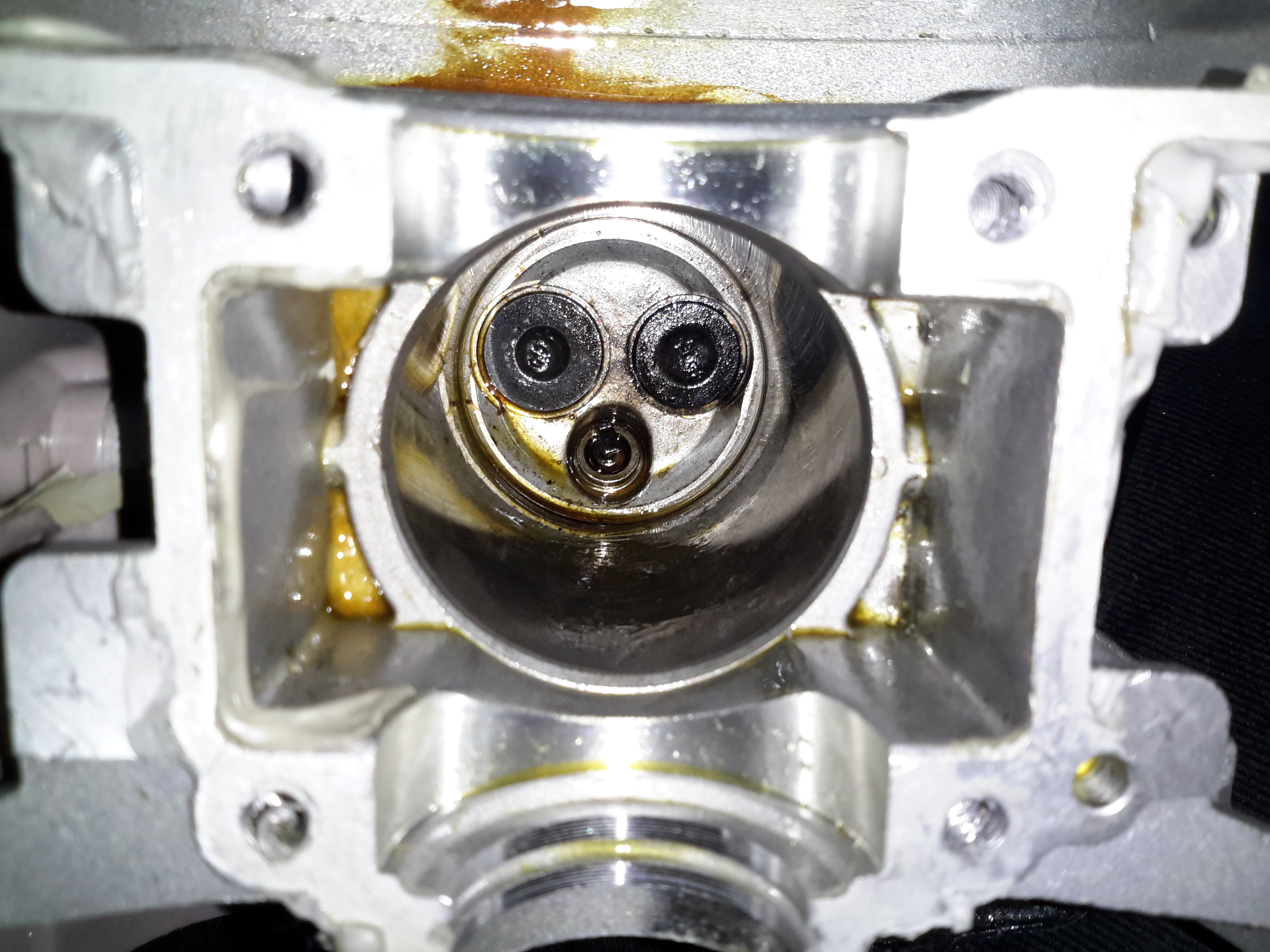
Cylinder Bore
A look up the cylinder bore shows the valves in the cylinder head. These engines, like their 2-stroke cousins have a single casting instead of a separate block & head, so getting at the valves is a little more of a pain. The cylinder bore itself is a cast-in iron liner and it’s totally smooth – like a mirror finish. There’s not a single sign of a crosshatch pattern from honing. If the first engine that died on me was the same – I’d be surprised if it wasn’t, this could easily cause ring breakage. The usual crosshatch pattern the cylinder hone produces holds oil, to better help lubricate the piston & rings. Without sufficient lubrication, the rings will overheat & expand far enough to close the end gap. Once this happens they will break.
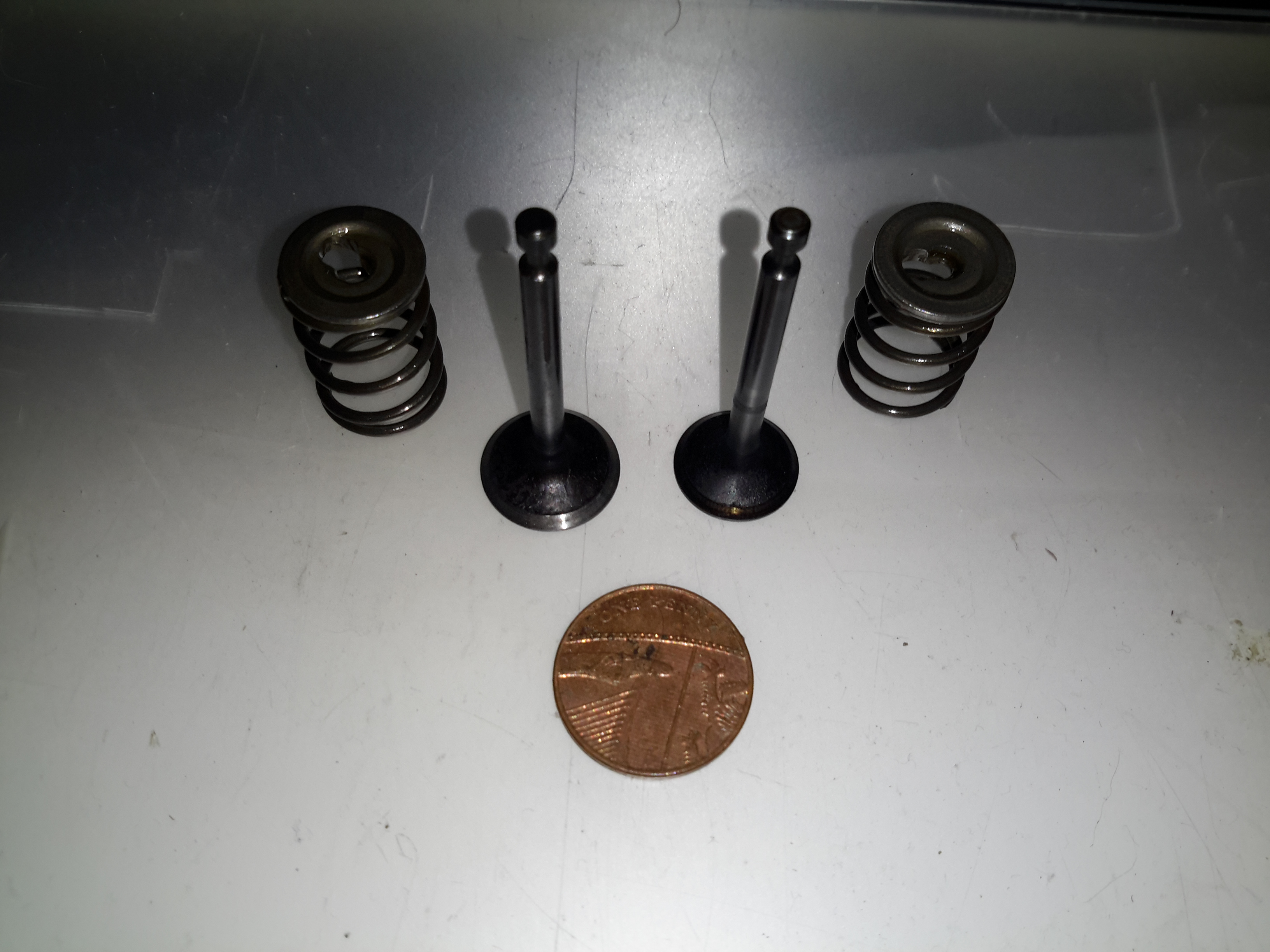
Engine Valves
Finally, here’s the valves with their springs removed from the cylinder. These are the smallest poppet valves I’ve ever seen, a British penny is provided for scale.
In all, these engines share many components with the older 2-stroke versions. The basic crankshaft & connecting rod setup is the same as I’ve seen in many old 2-strokes previous, the addition of the rather ingenious oiling system by Honda is what makes these tiny 4-strokes possible. I definitely won’t be trusting these very cheap copies in any of my projects, reliability is questionable at the least. The apparent lack of cooling air flow over the cylinder from the flywheel fan is concerning, along with the corner-cutting on the cylinder finishing process & piston crown, presumably to reduce factory costs.
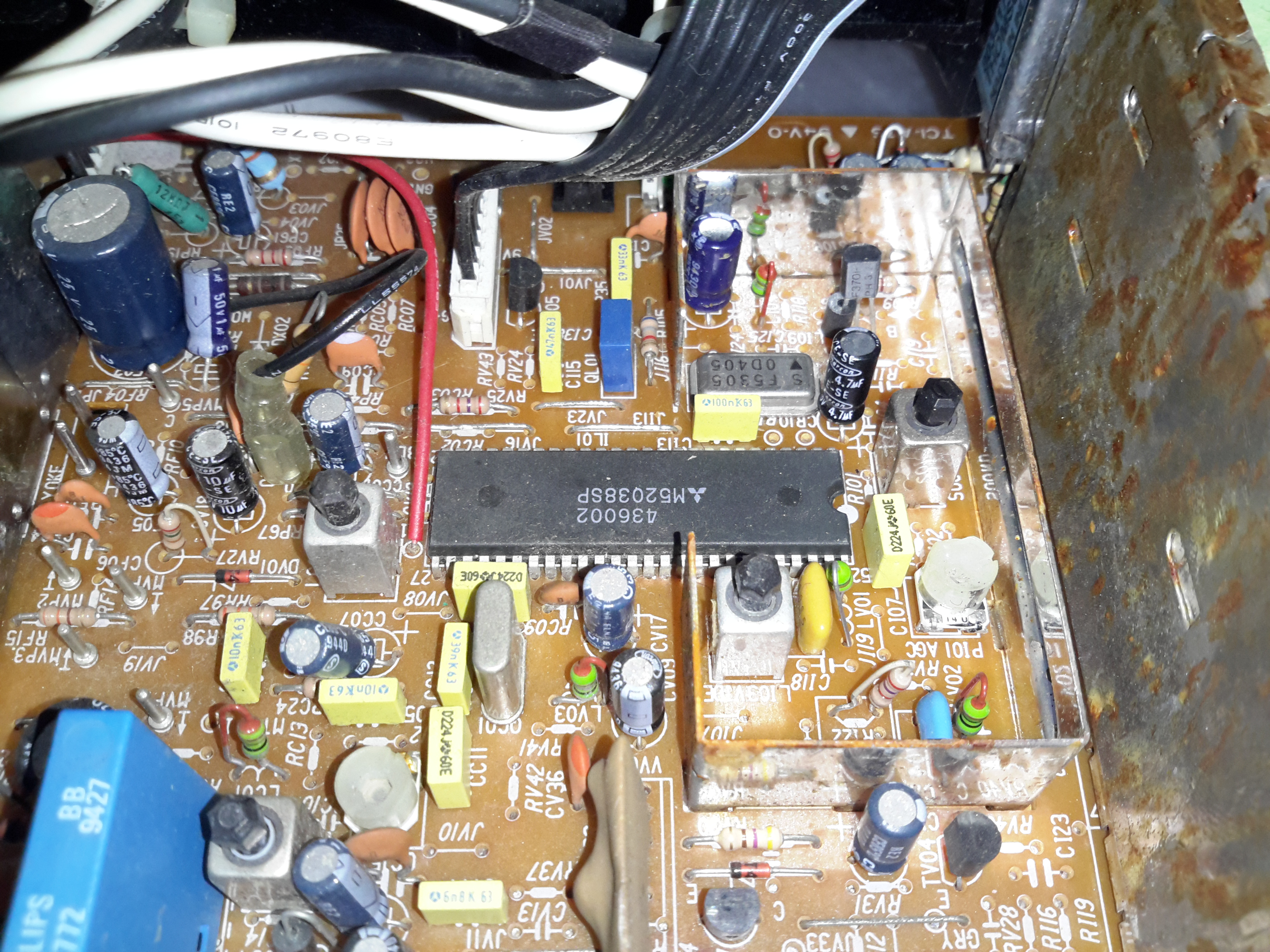
Here’s the other TV that was picked up from the local water point having been put of to be recycled. This one is much newer than the Thorn TV, a 10″ colour version from Ferguson.
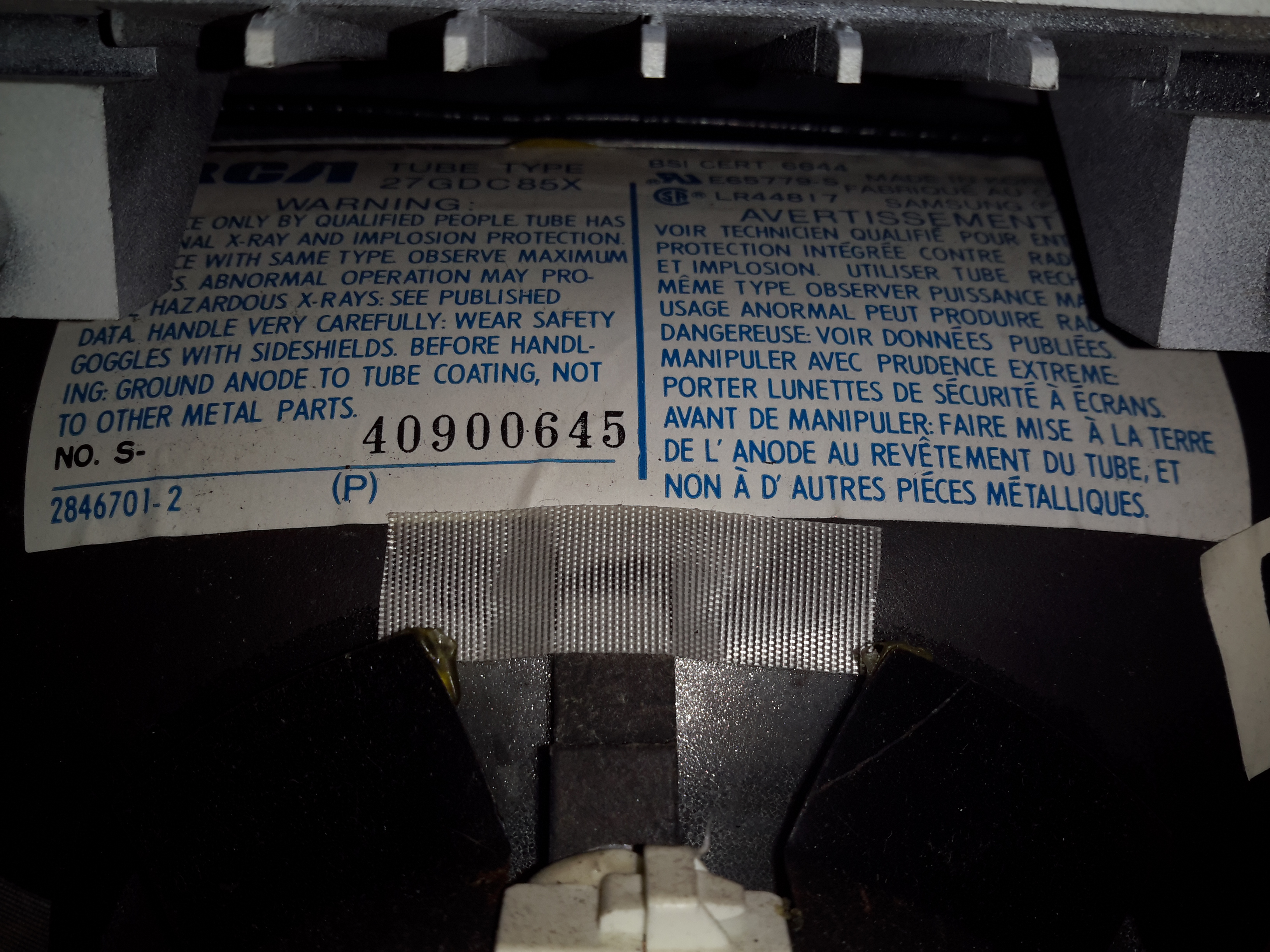
RCA 27GDC85X CRT
The colour CRT used is an RCA branded one, 27GDC85X.
Power Inputs
Like the other TV, this one is dual voltage input, mains 240v & 12v battery. This TV is a factory conversion of a standard 240v AC chassis though.
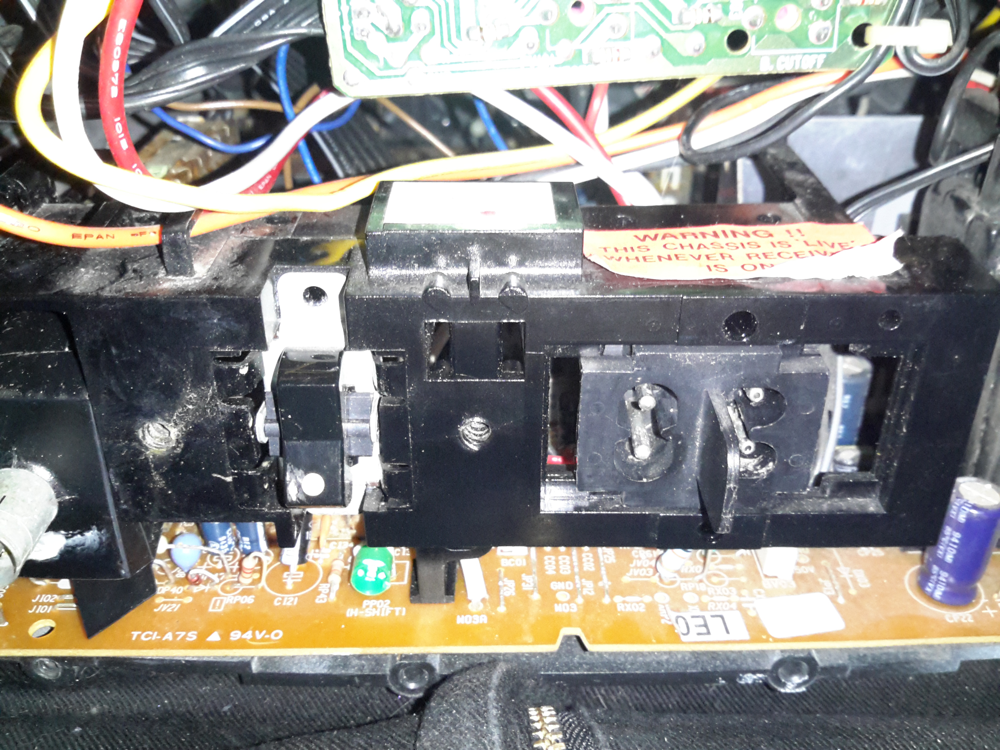
HV PSU
The 12v power first goes into this board, which looked suspiciously like an inverter. Measuring on the output pins confirmed I was right, this addon board generates a 330v DC supply under a load, but it’s not regulated at all, under no load the output voltage shoots up to nearly 600v!
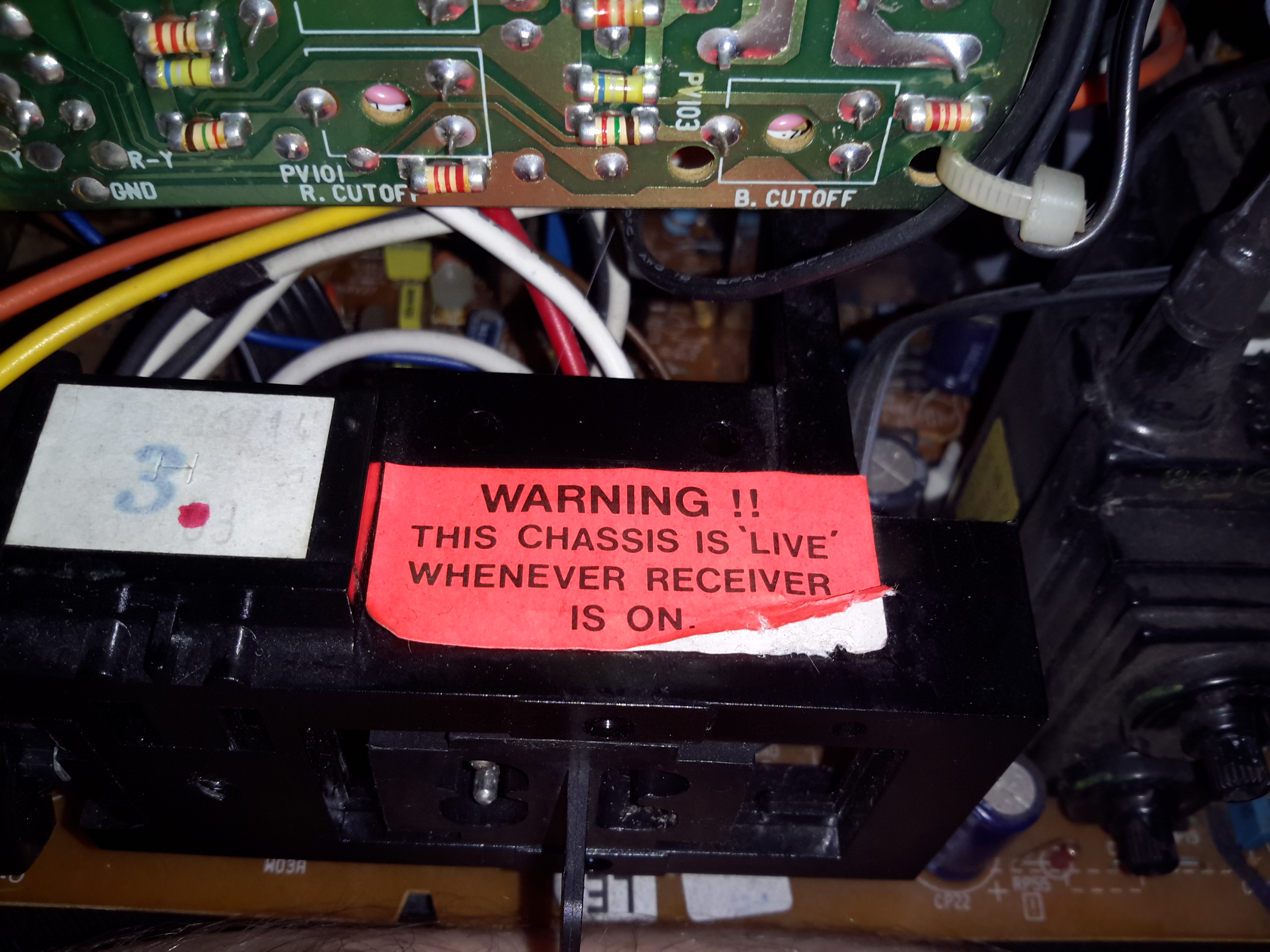
Live Chassis
I’ve not seen one of these labels on a TV for many years, when back in the very old TV sets the steel chassis would be used to supply power to parts of the circuitry, to save on copper. Although it doesn’t have a metal chassis to actually become live, so I’m not sure why it’s here.
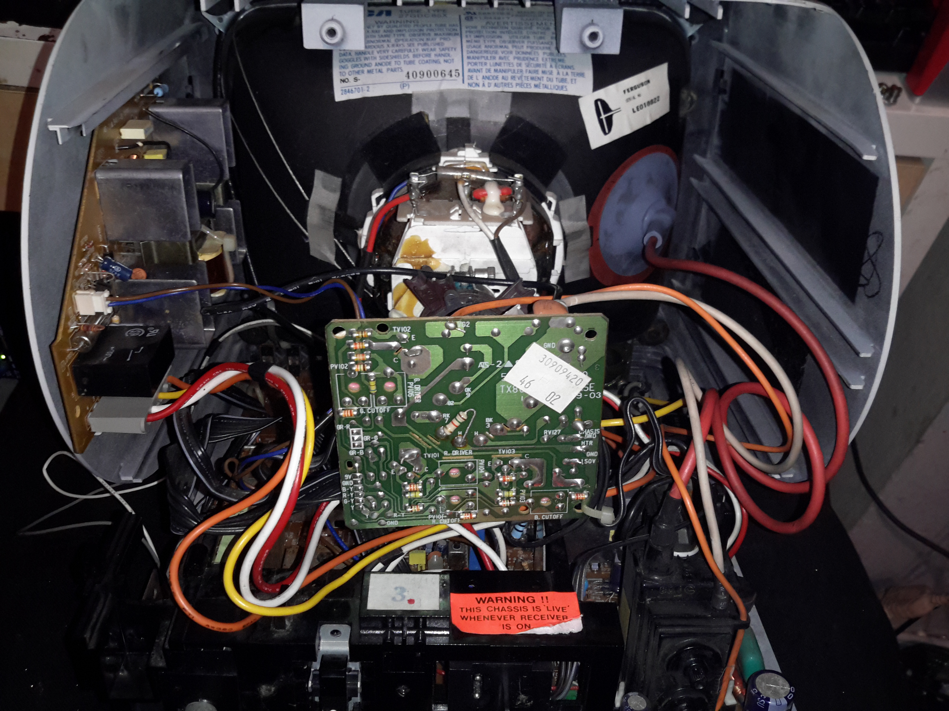
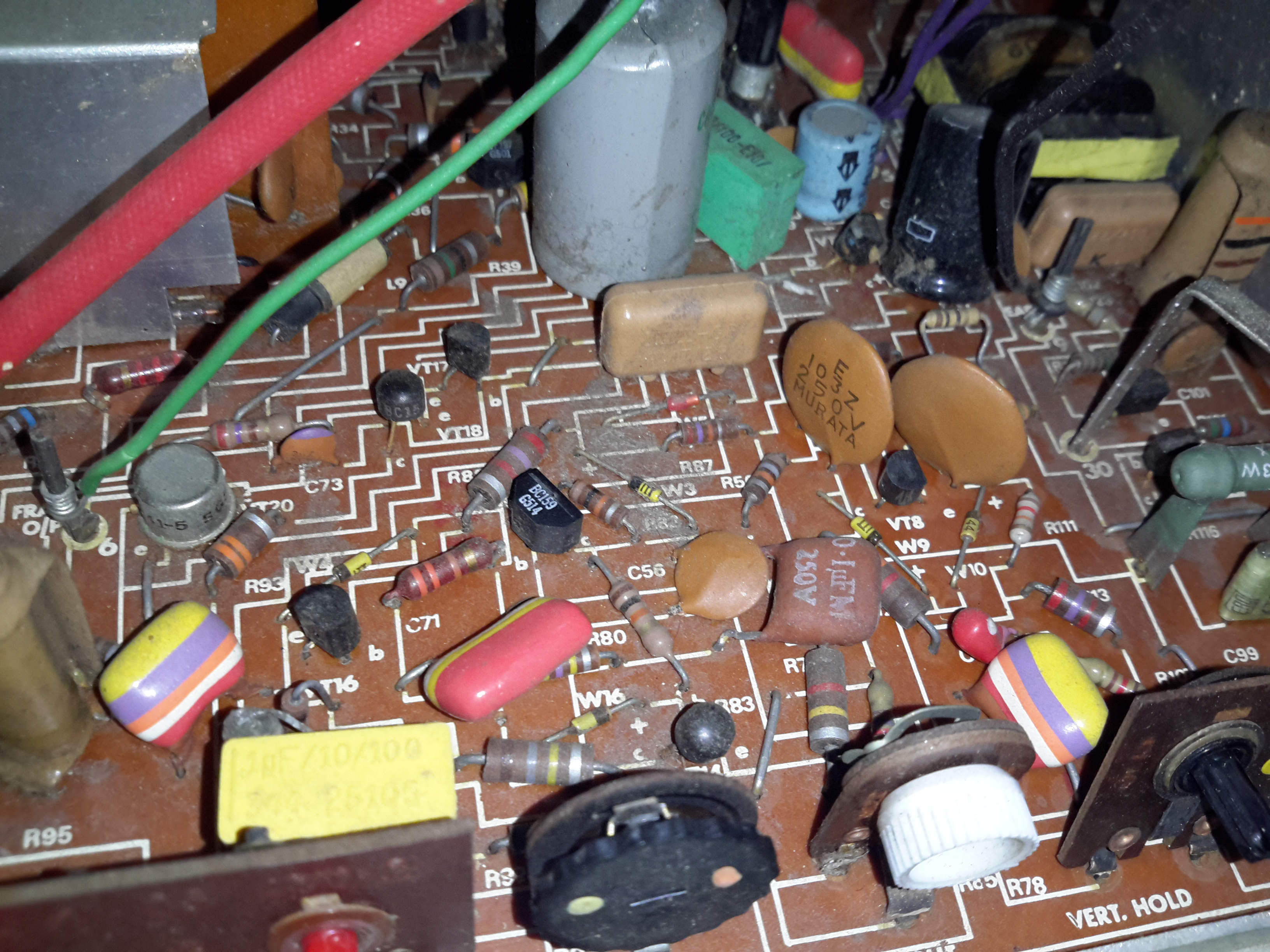
Main PCB
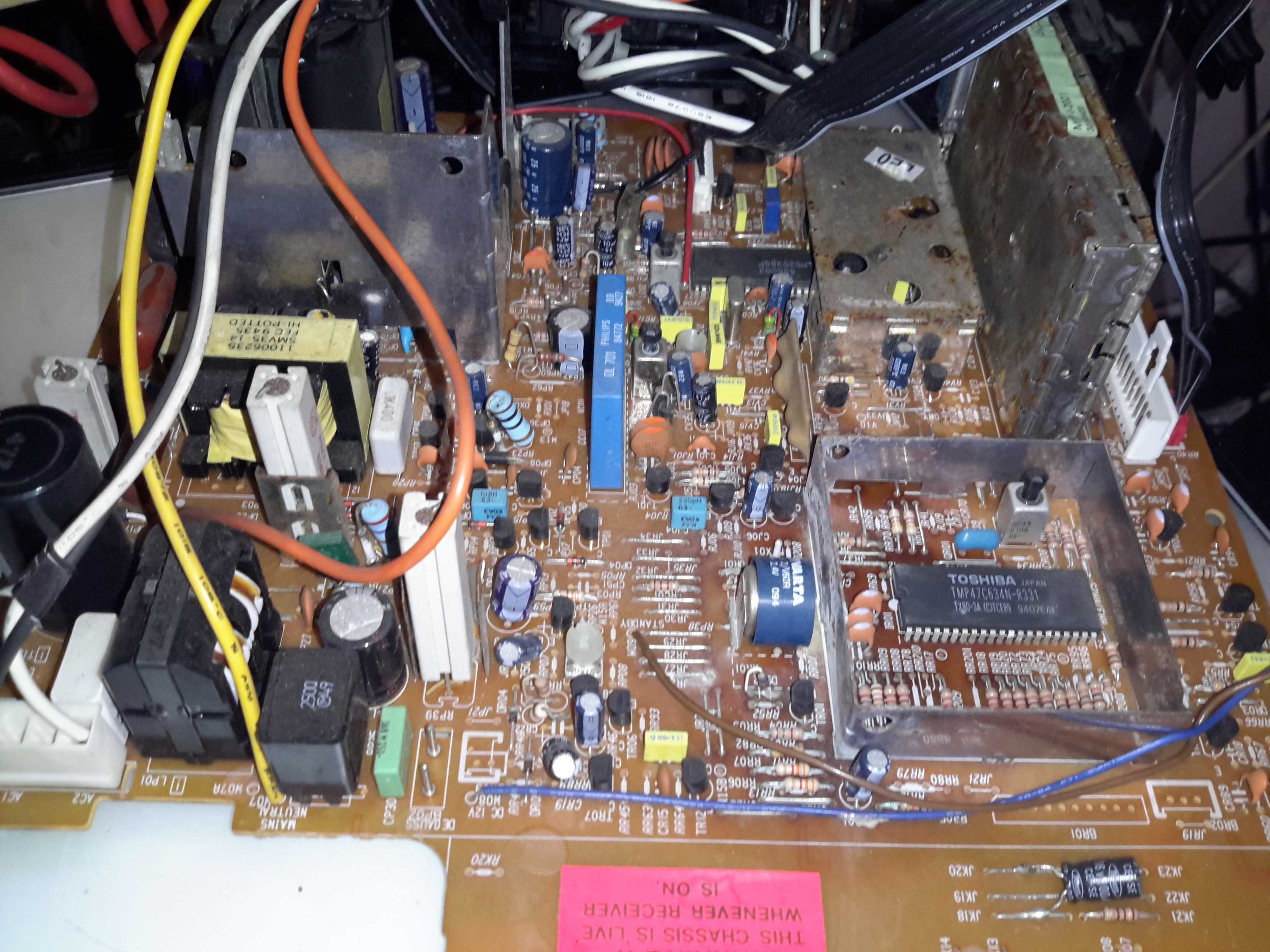
The main PCB is much more integrated in this newer TV, from the mid 90’s, everything is pretty much taken care of by silicon by this point.
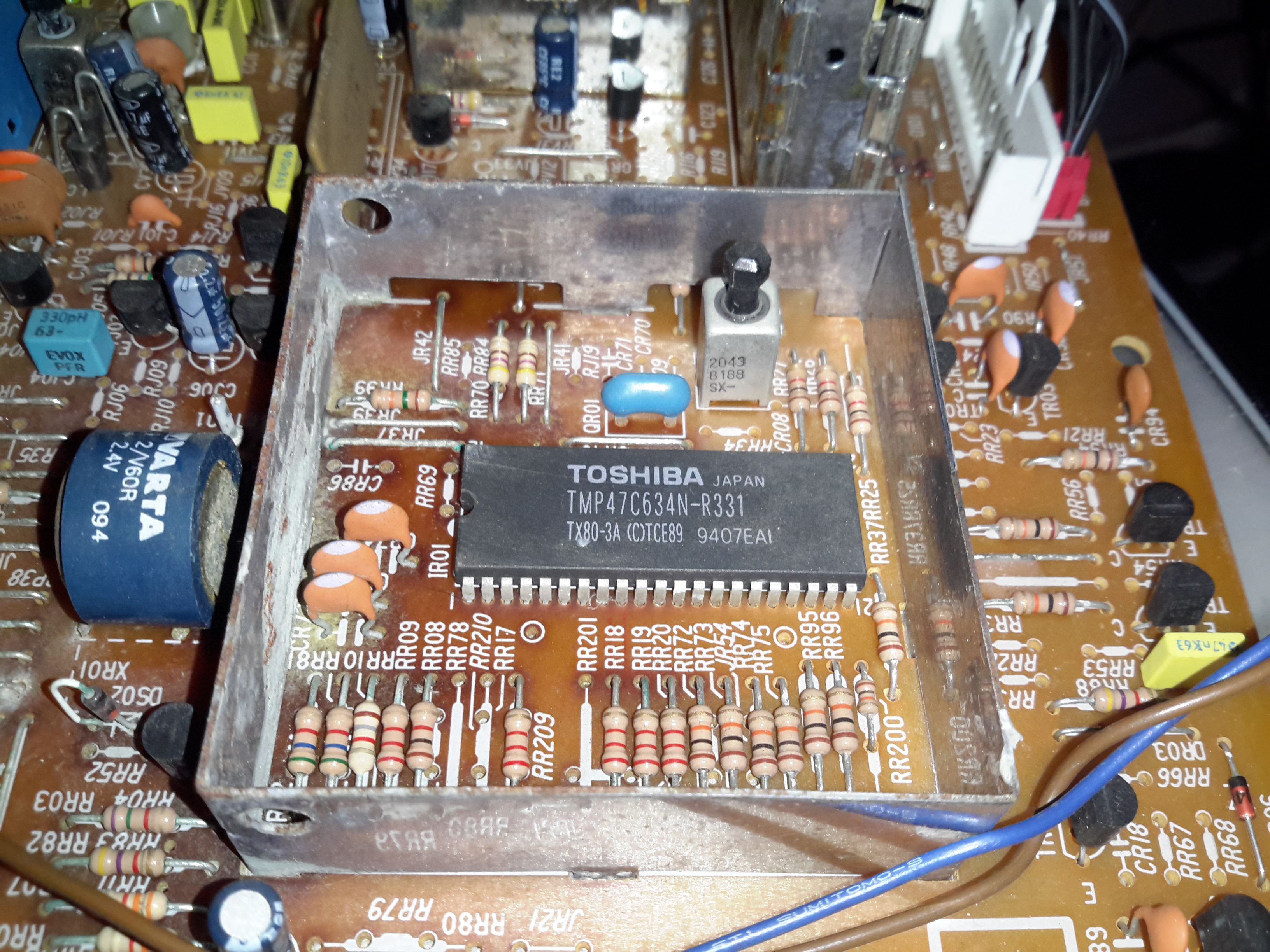
Main Microcontroller
This Toshiba µC takes care of channel switching & displaying information on the CRT. The tuner in this TV is electronically controlled.
PAL Signal Processor
The video signal is handled by this Mitsubishi IC, which is a PAL Signal Processor, this does Video IF, Audio IF, Chroma, & generates the deflection oscillators & waveforms to drive the yoke.
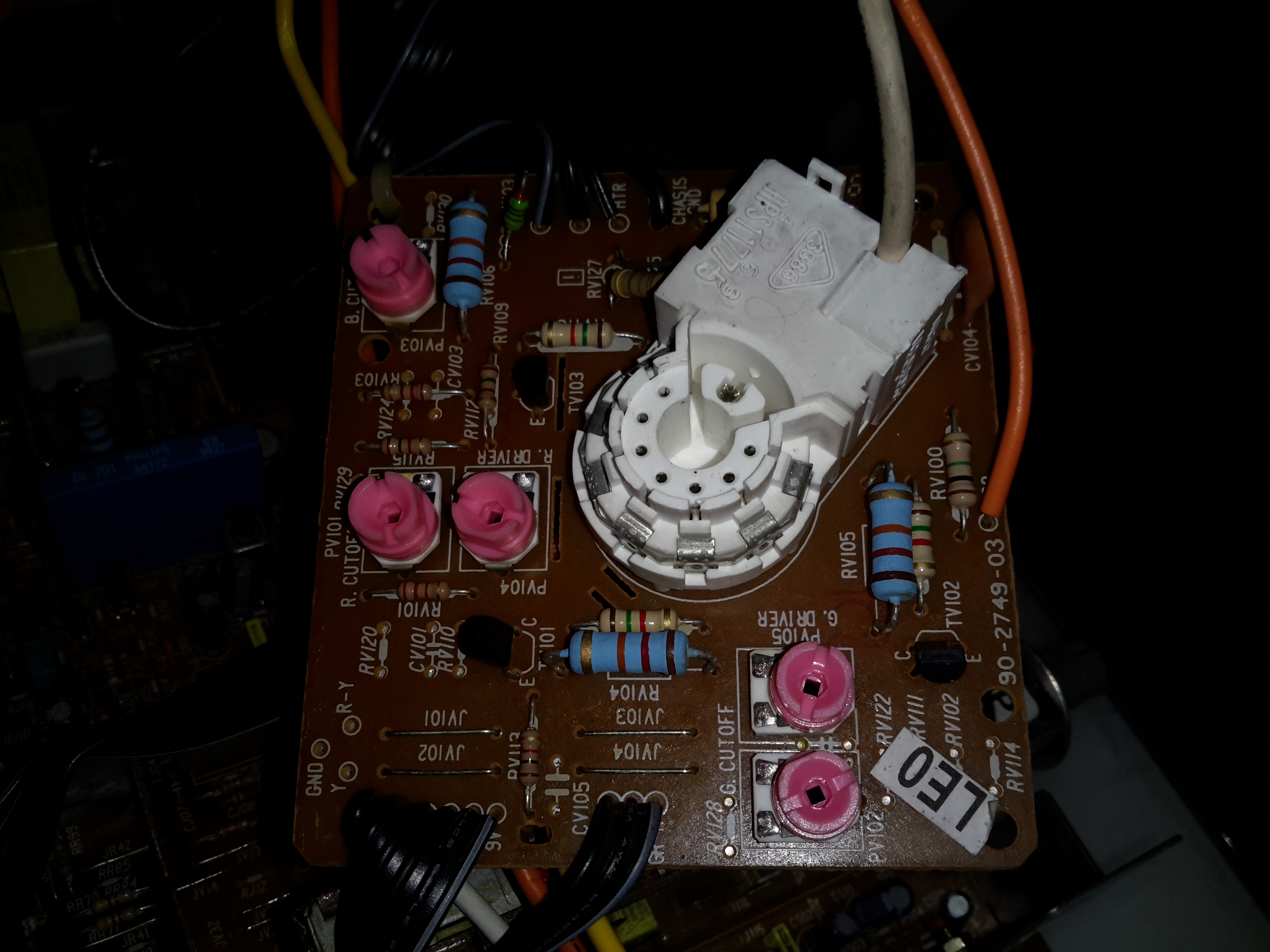
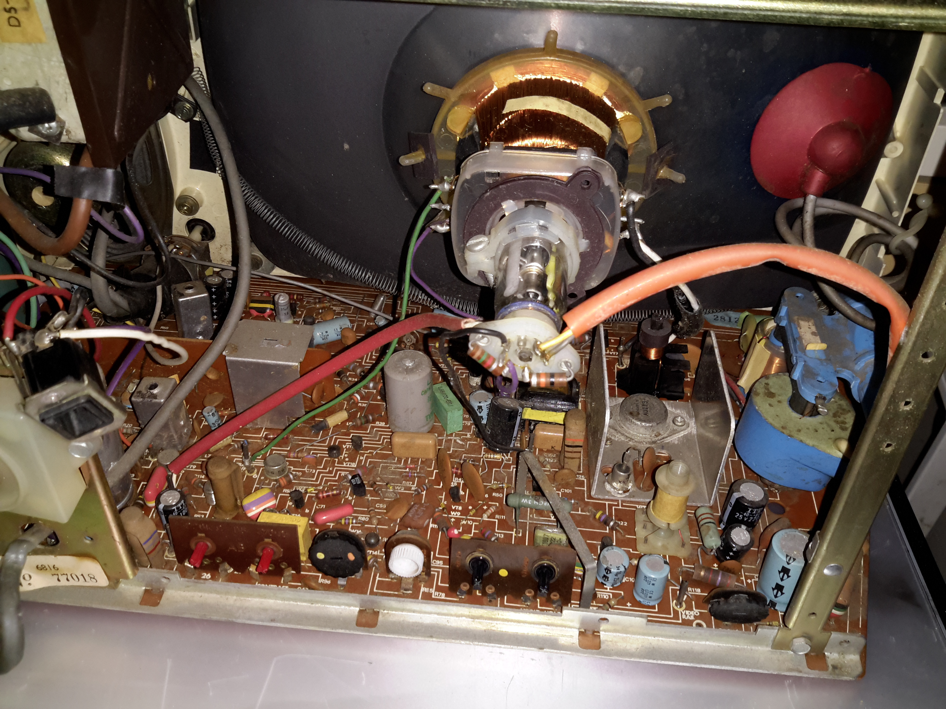
CRT Adjustments
There are some adjustments on the CRT neck board for RGB drive levels & cutoff levels. This board also had the final video amplifiers onboard, which drive the CRT cathodes.
The other day at the local canal-side waterpoint, this TV was dumped for recycling, along with another later model Colour TV. This is a 1970’s Black & White mains/battery portable made by Thorn. It’s based on a common British Radio Corporation 1590 chassis. Having received a soaking from rain, I didn’t expect this one to work very well.
Tuner
Being so old, there is no electronic control of the tuner in this TV, and only has the capability to mechanically store 4 different channels. The tuner itself is a cast box with a plastic cover.
Tuning Lever
The mechanical buttons on the front of the TV push on this steel bar, by different amounts depending on the channel setting. This bar is connected to the tuning capacitor inside the tuner.
Tuner Compartments
Unclipping the plastic cover, with it’s lining of aluminium foil for shielding reveals the innards of the tuner module.
Tuner Input Stage
Here’s the tuner front end RF transistor, which has it’s can soldered into the frame, this is an AF239 germanium UHF transistor, rated at up to 900MHz.
Tuner IF Mixer Stage
As the signal propagates through the compartments of the tuner, another transistor does the oscillator / IF mixing, an AF139 germanium, rated to 860MHz.
Tuning Capacitor
As the buttons on the front of the set are pushed, moving the lever on the outside, the tuning capacitor plates intermesh, changing the frequency that is filtered through the tuner. The outer blades of the moving plates are slotted to allow for fine tuning of the capacitance, and therefore transmitted frequency by bending them slightly.
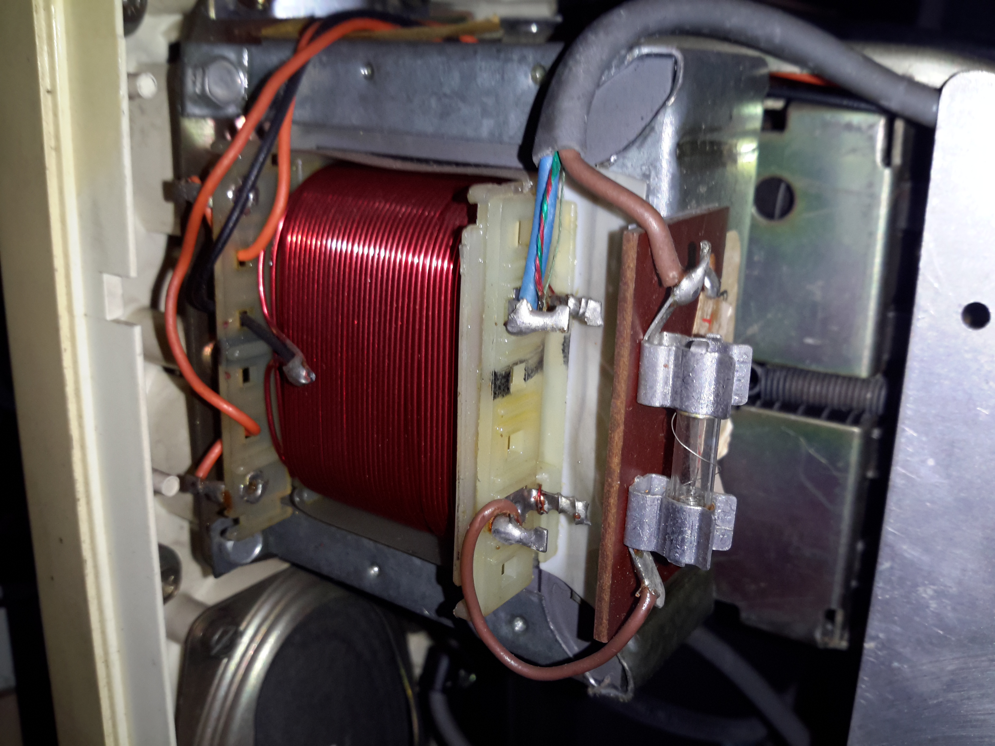
Mains Transformer
Being a dual supply TV that can operate on either 12v battery power or mains, this one has a large centre tapped mains transformer that generates the low voltage when on AC power. Full wave rectification is on the main PCB. The fuse of this transformer has clearly been blown in the past, as it’s been wound with a fine fuse wire around the outside to repair, instead of just replacing the fuse itself.
Chassis Rear
The back of the set has all the picture controls on the bottom edge, with the power input & antenna connections on the left just out of shot. The CRT in this model is an A31-120W 12″ tube, with a really wide deflection angle of 110°, which allows the TV to be smaller.
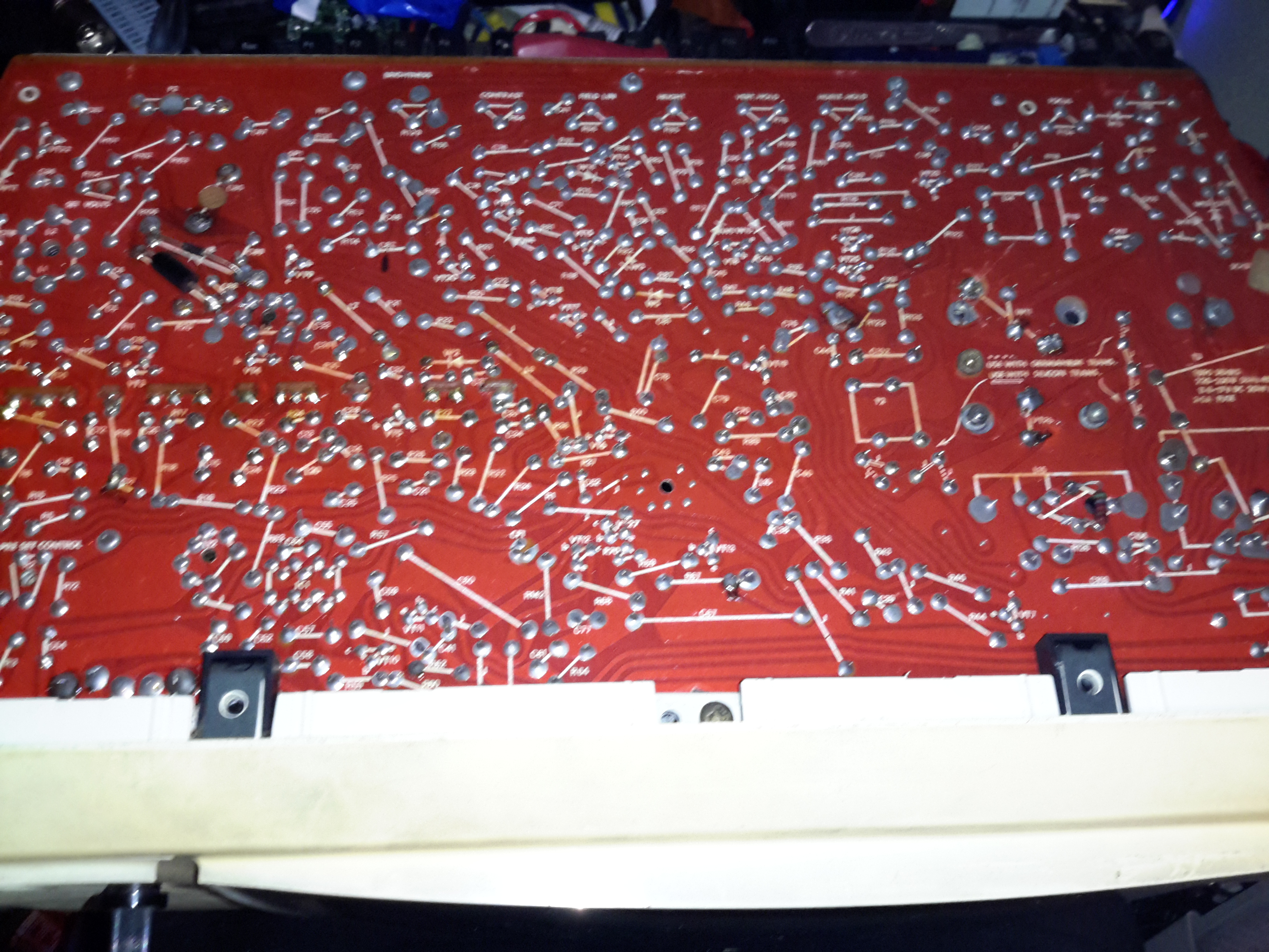
Main PCB
The bottom of the mainboard has all the silkscreen markings for the components above which certainly makes servicing easier 😉 This board’s copper tracks would have been laid out with tape, obviously before the era of PCB design software.
Components
The components on this board are laid out everywhere, not just in square grids. The resistors used are the carbon composition type, and at ~46 years old, they’re starting to drift a bit. After measuring a 10K resistor at 10.7K, all of these would need replacing I have no doubt. Incedentally, this TV could be converted to take a video input without the tuner, by lifting the ferrite beaded end of L9 & injecting a signal there.
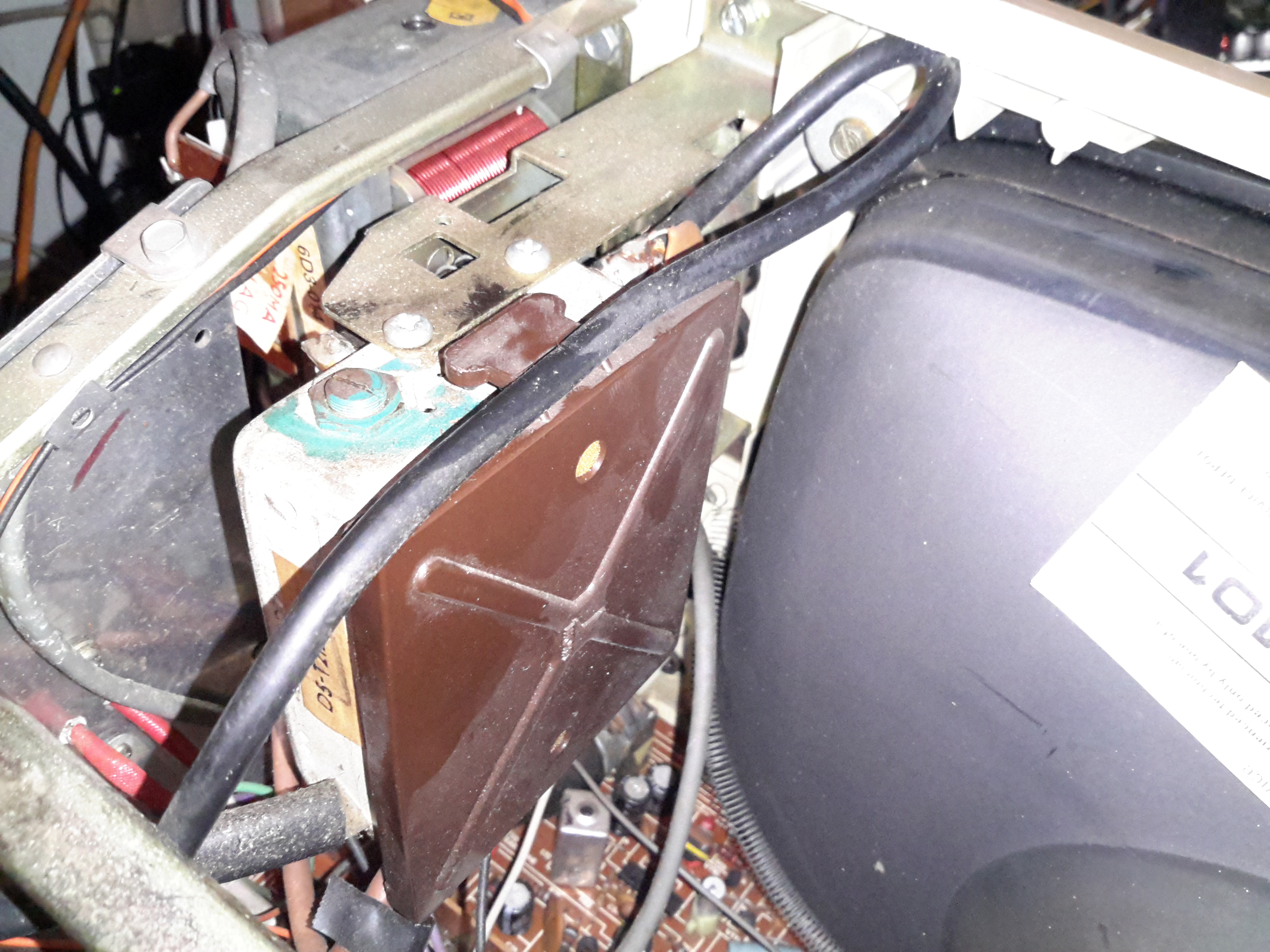
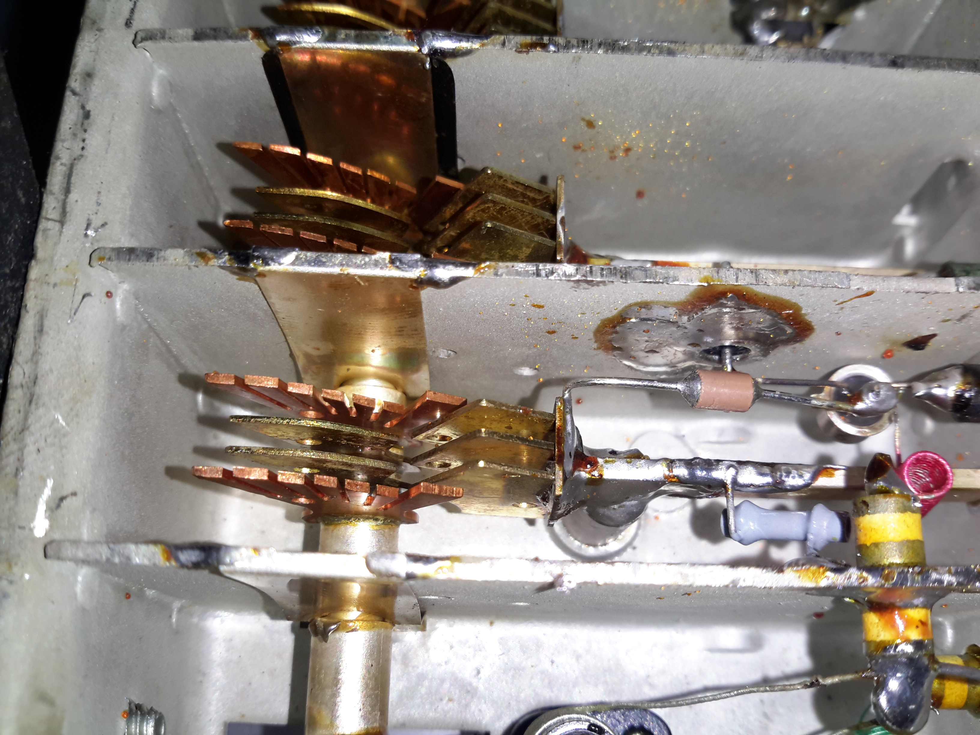
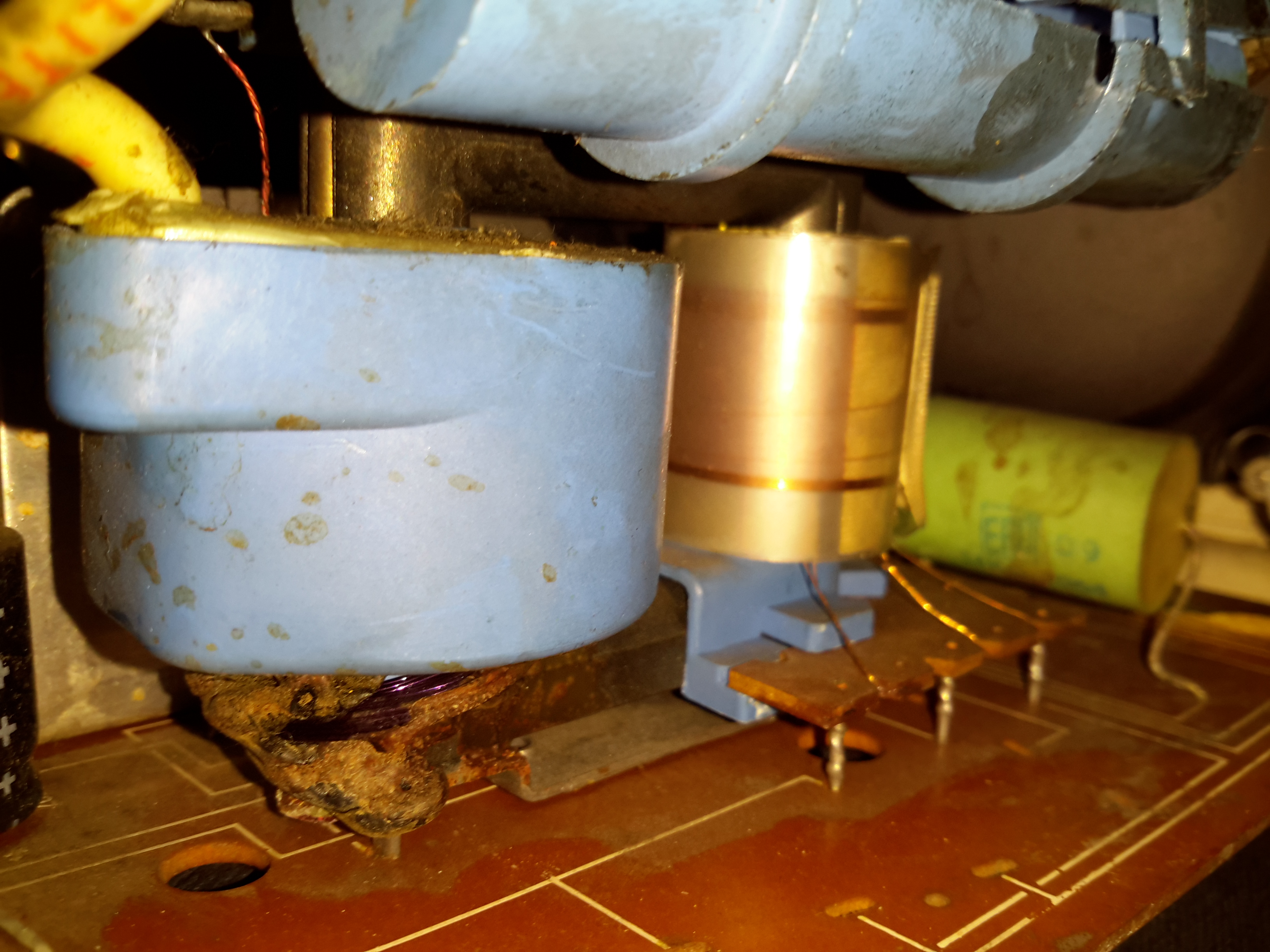
Flyback Primary Windings
The flyback (Line Output Transformer) is of the old AC type, with the rectifier stack on top in the blue tube, as opposed to more modern versions that have everything potted into the same casing. The primary windings are on the other leg of the ferrite core, making these transformers much more easily repairable. This transformer generates the 12kV required for the CRT final anode, along with a few other voltages used in the TV, for focussing, etc.
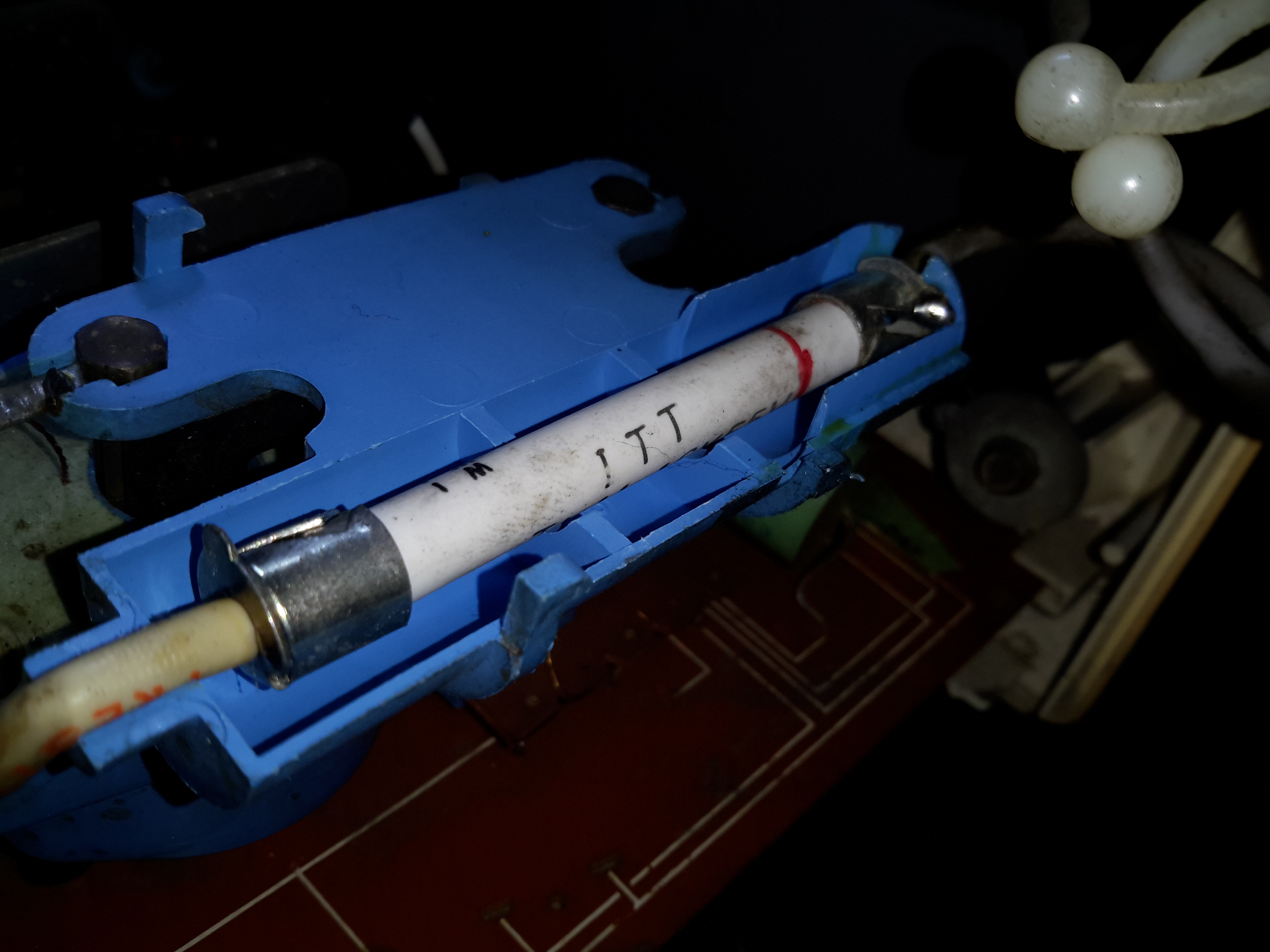
Rectifier Stack
The main EHT rectifier stack looks like a huge fuse, inside the ceramic tube will be a stack of silicon diodes in series, to withstand the high voltage present.
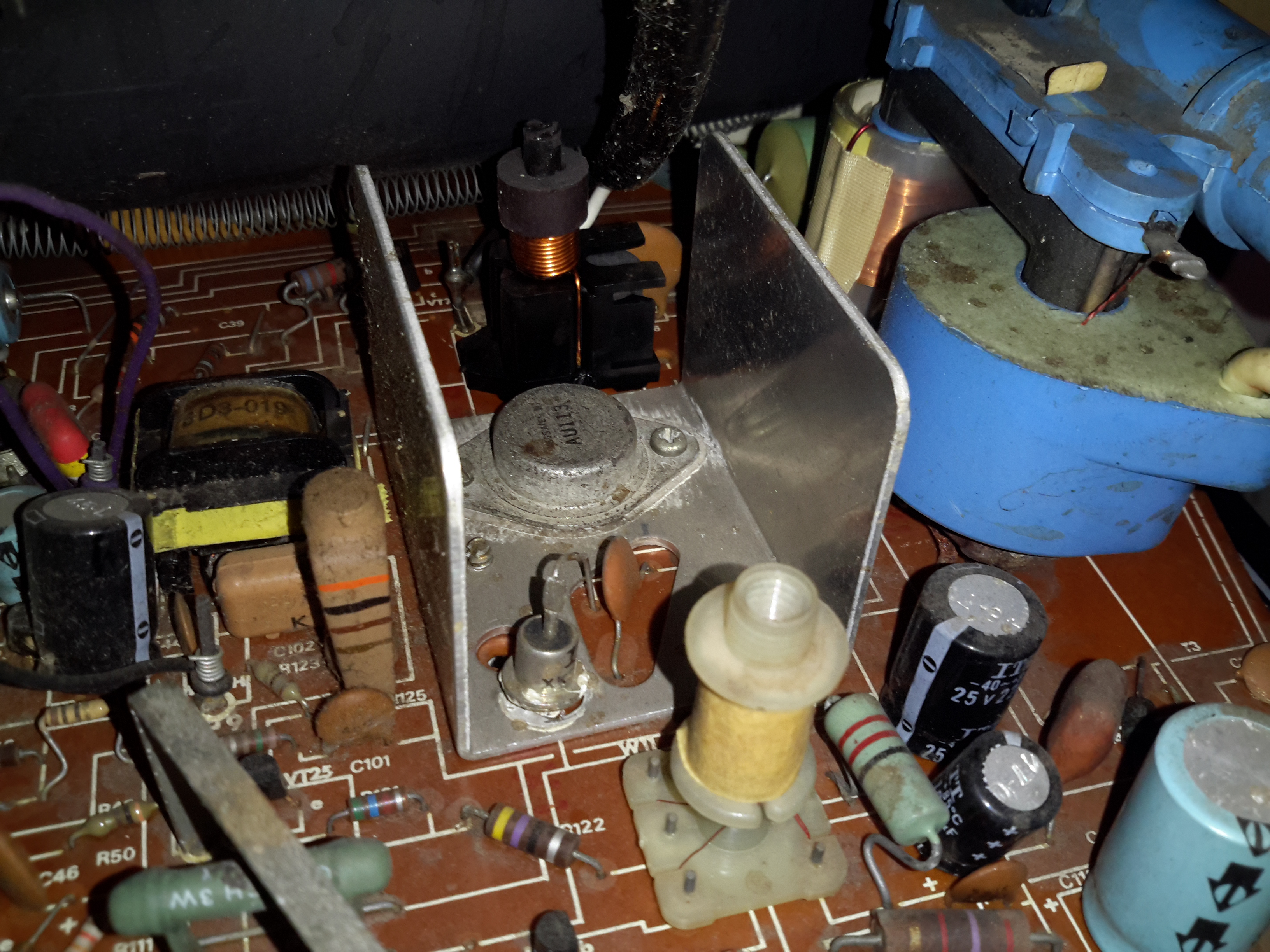
Horizontal Output Transistor
This is the main switching transistor that drives the flyback, the HOT. This is an AU113, another germanium type, rated at 250v 4A. The large diode next to the transistor is the damper.
I’ve managed to find all the service information for this set online, link below!
[download id=”5616″]
More to come if I manage to get this TV working!
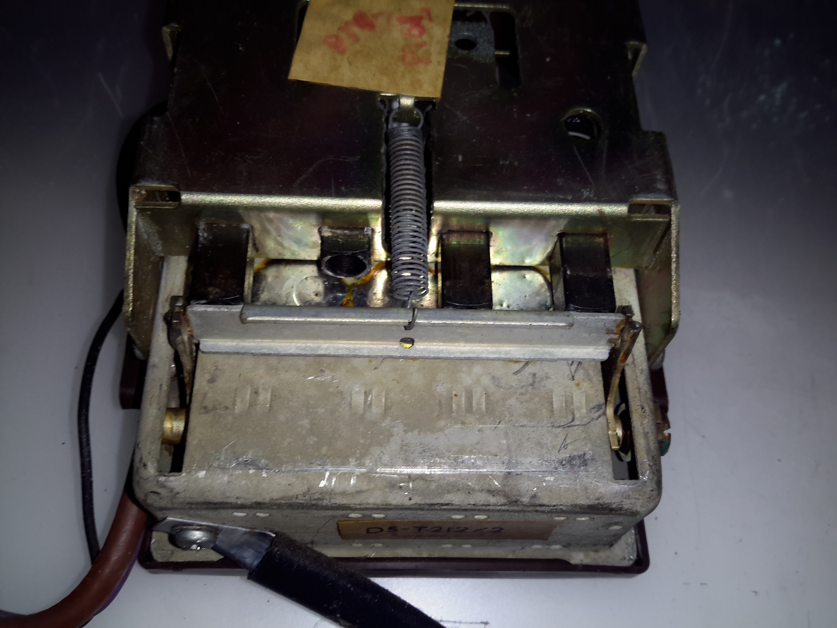
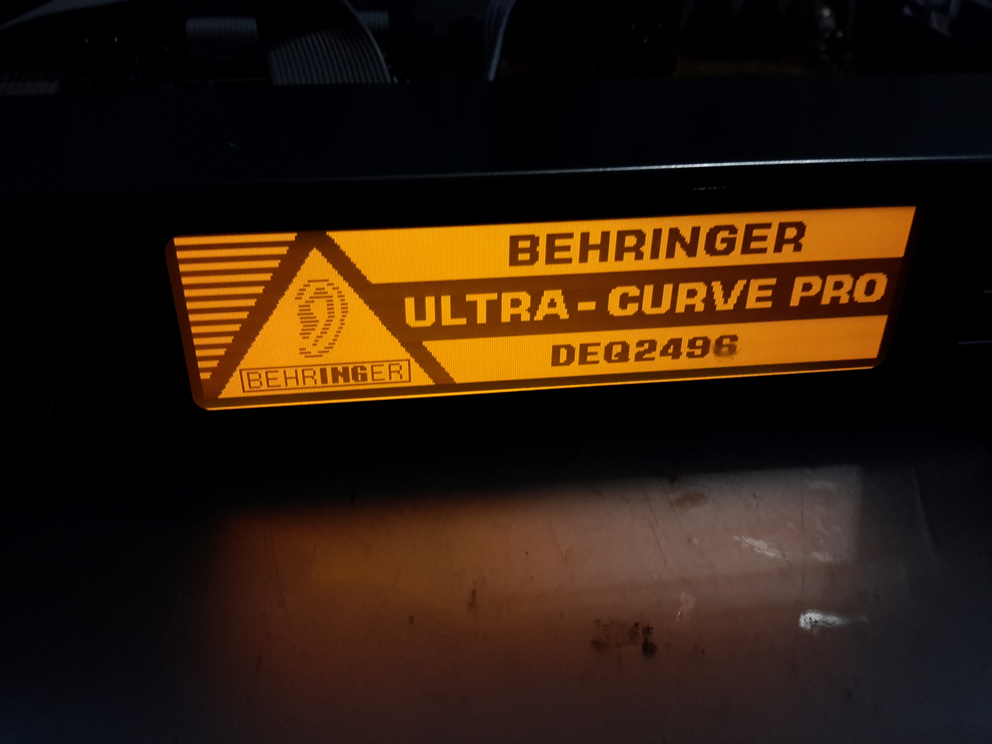
I was recently given this unit, along with another Behringer sound processor to repair, as the units were both displaying booting problems. This first one is a rather swish Mastering Processor, which has many features I’ll leave to Behringer to explain 😉
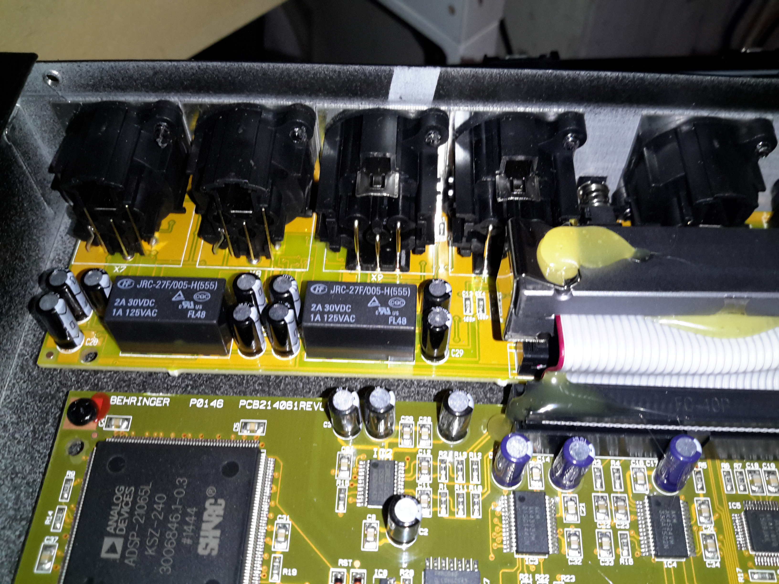
Input Board & Relays
All the inputs are on the back of this 19″ rackmount bit of kit, nothing much on this PCB other than the connectors & a couple of switching relays.
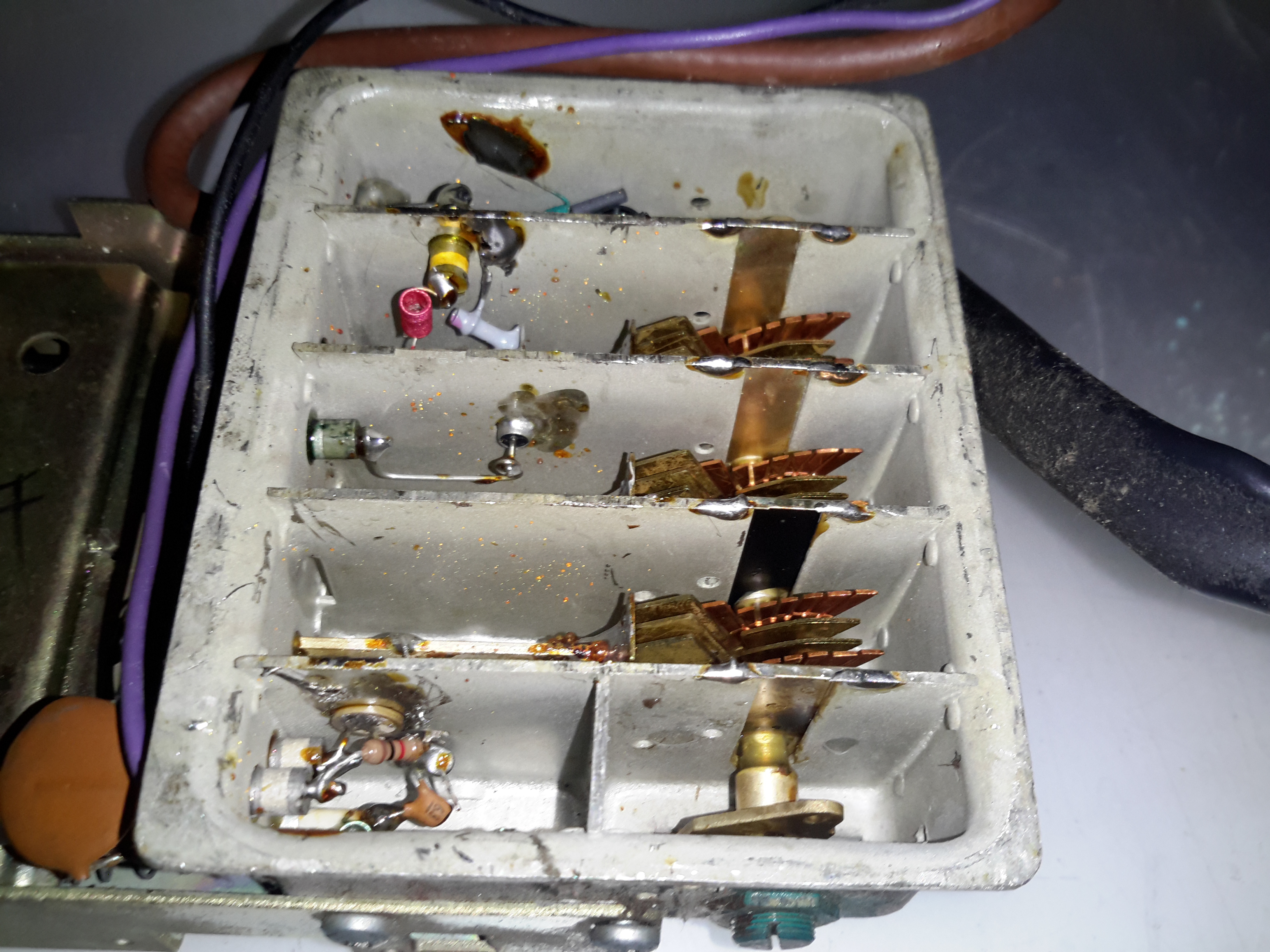
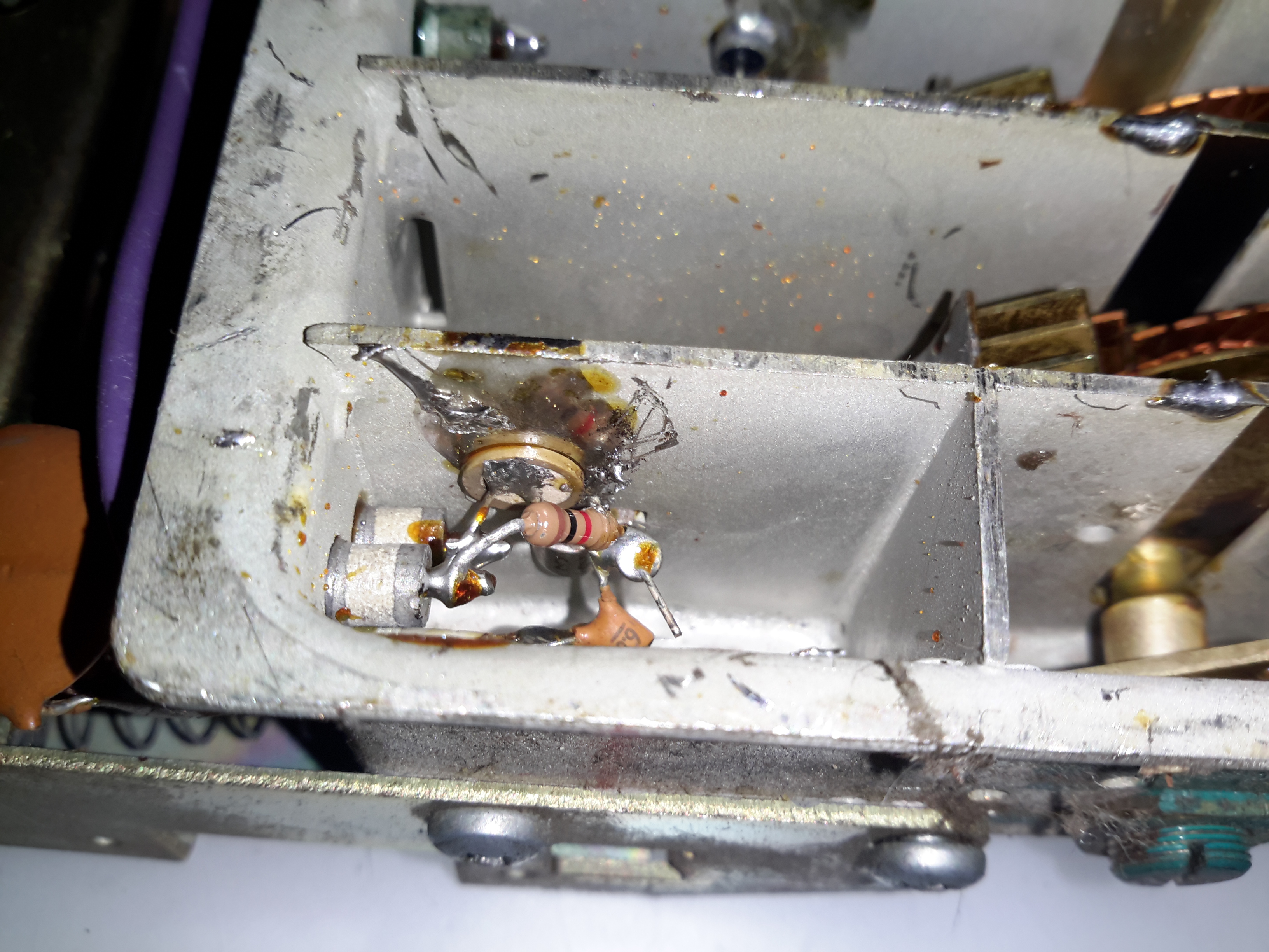
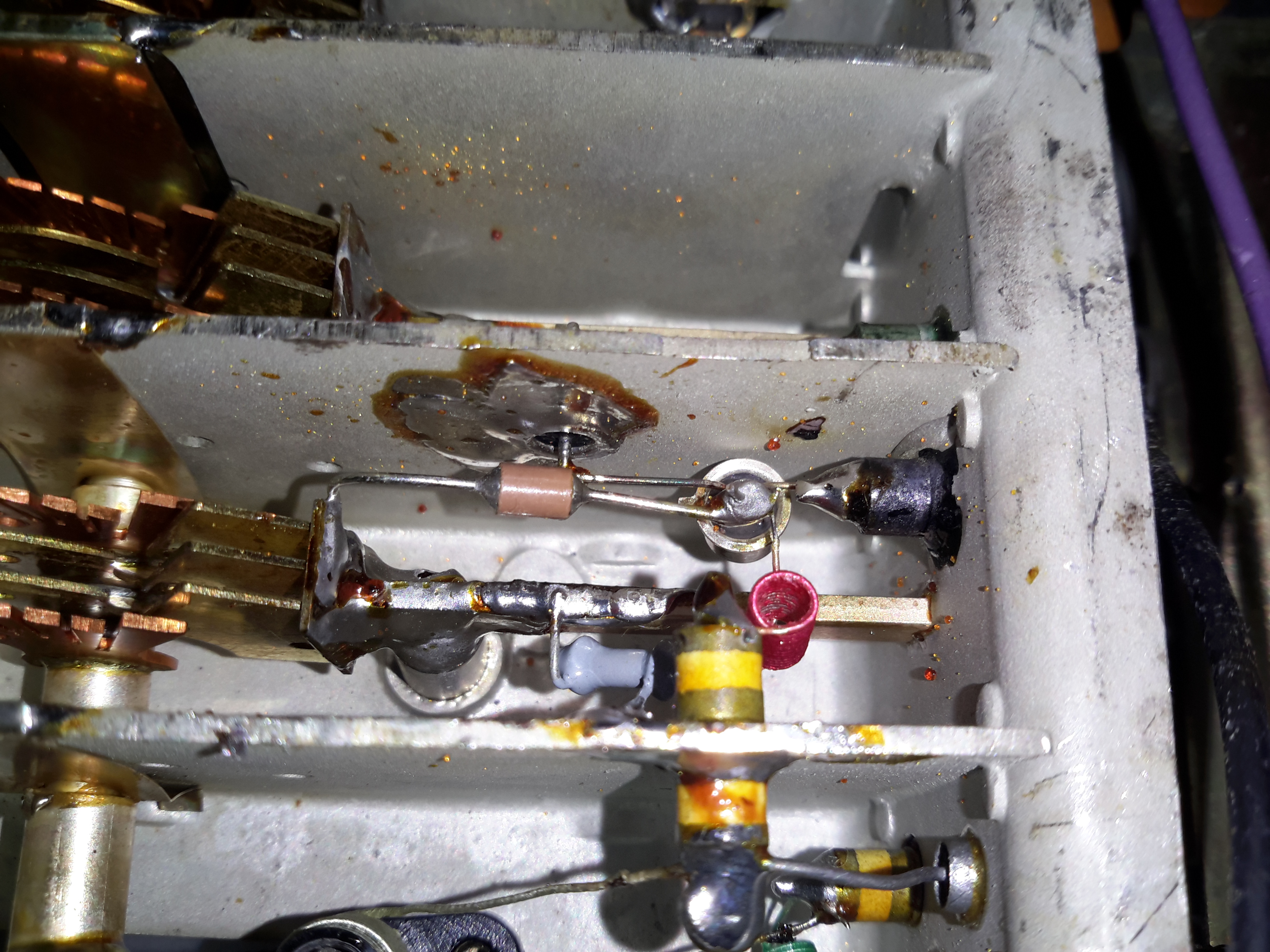
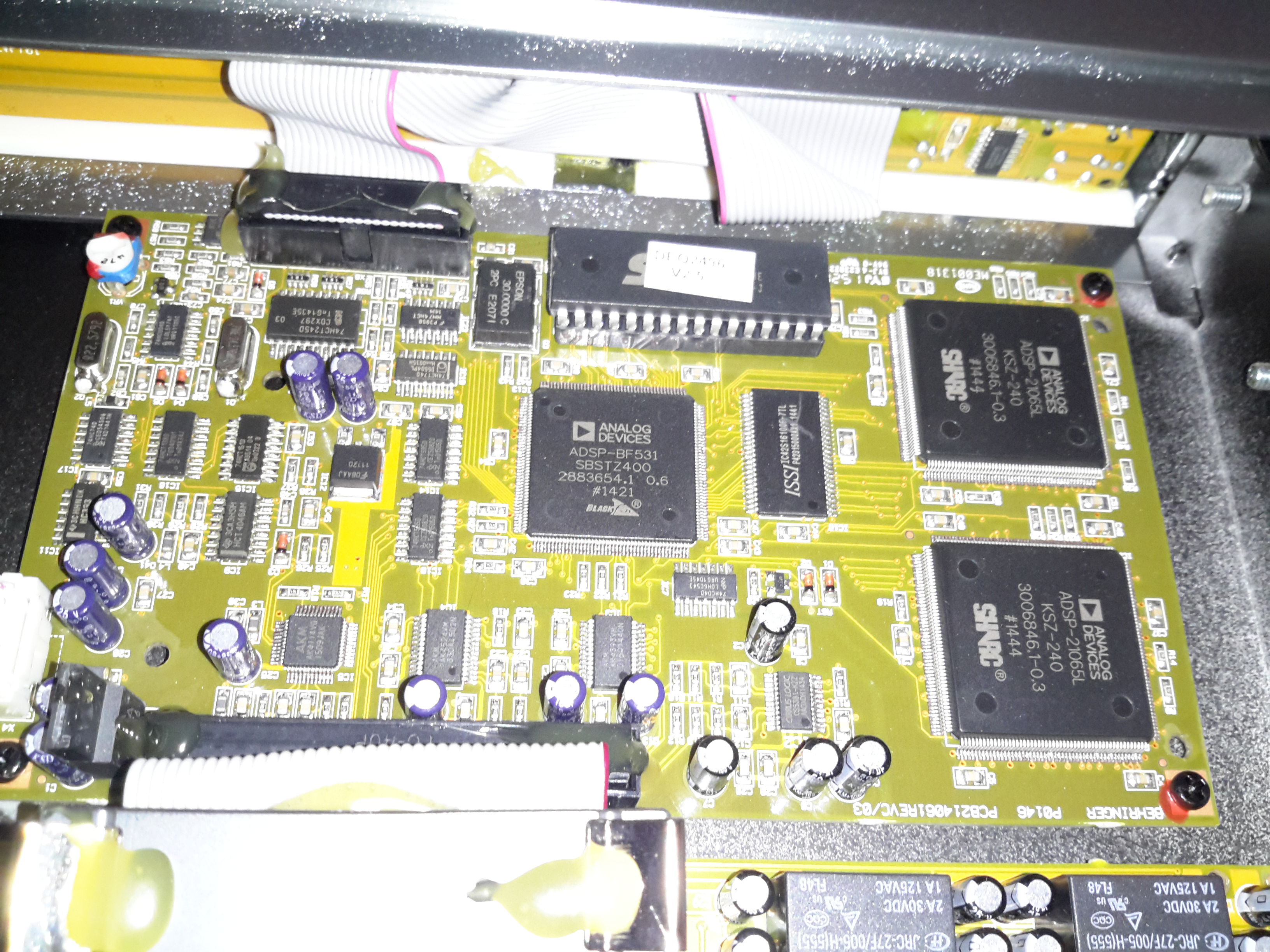
Main Processor PCB
All the magic is done on the main processor PCB, which is host to 3 Analog Devices DSP processors:
ADSP-BF531 BlackFin DSP. This one is probably handling most of the audio processing, as it’s the most powerful DSP onboard at 600Mhz. There’s a ROM on board above this for the firmware & a single RAM chip. On the right are a pair of ADSP-21065 DSP processors at a lower clock rate of 66MHz. To the left is some glue logic to interface the user controls & dot-matrix LCD.
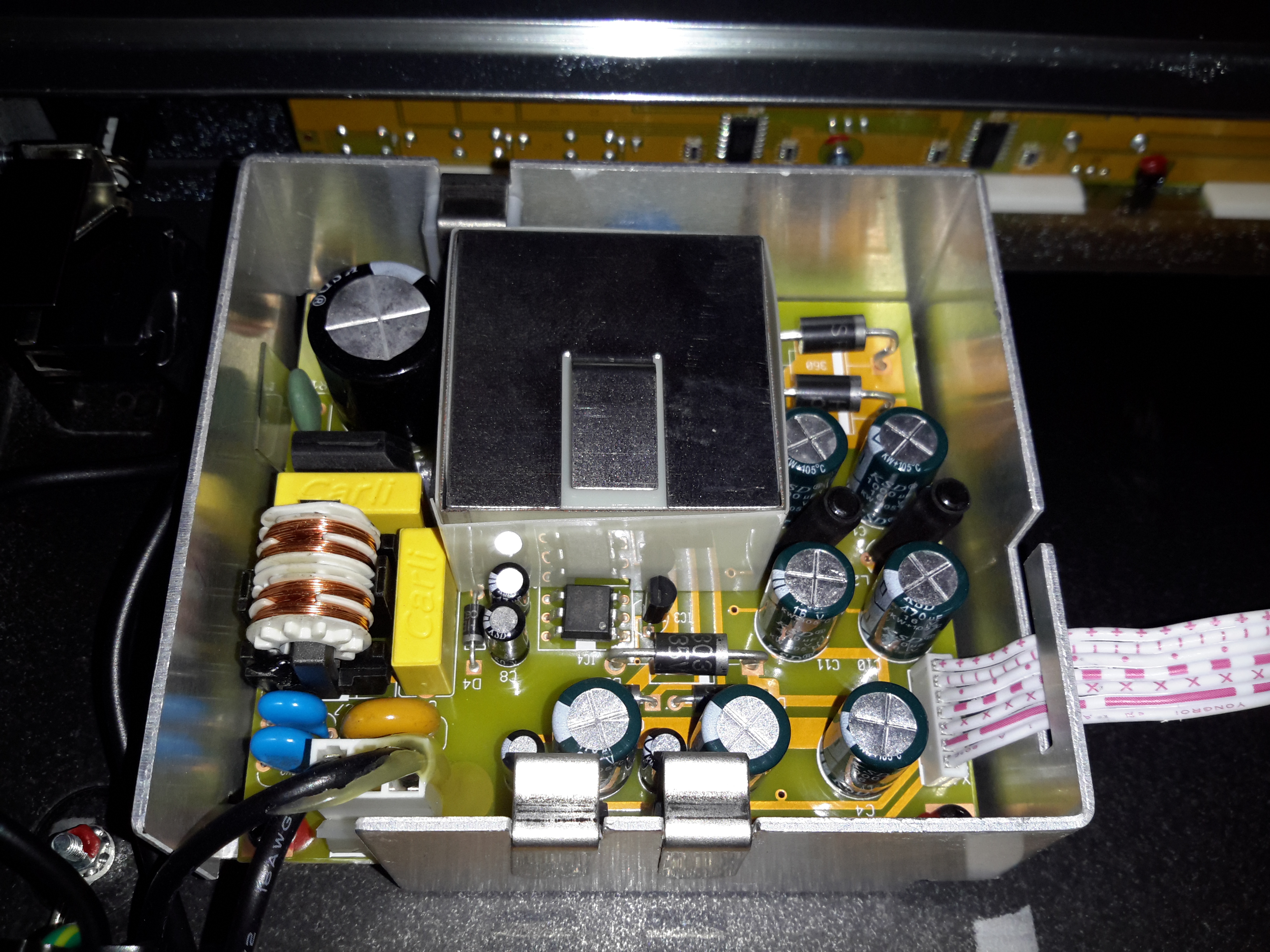
PSU Module
The PSU in this unit is a pretty standard looking SMPS, with some extra noise filtering & shielding. The main transformer is underneath the mu-metal shield in the centre of the board.
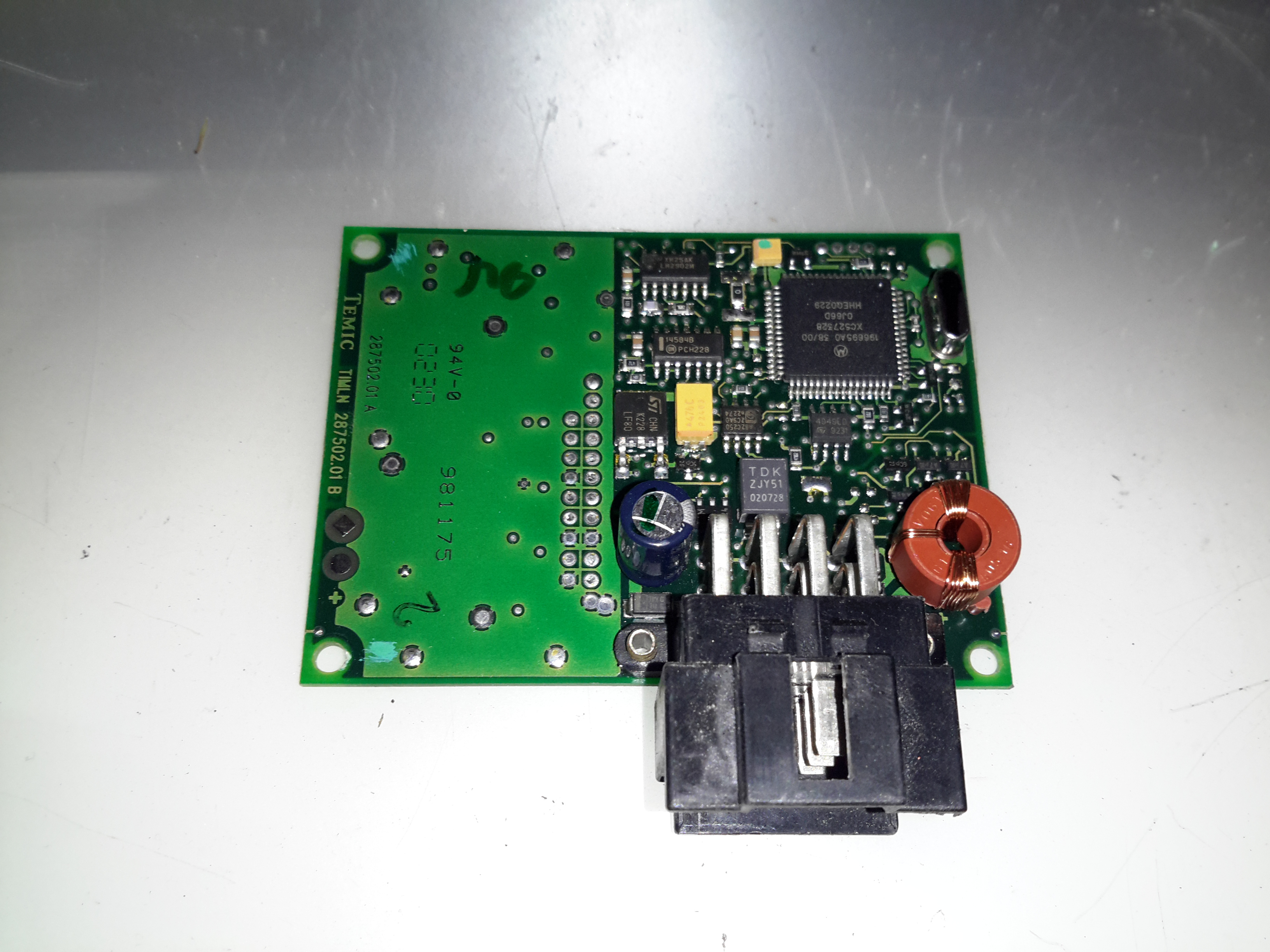
The other day I was given a random pile of car electronic parts from the scrap bin at the local garage, so I decided to do a few teardowns. This first one is a Temic Central Locking / Immobiliser module from a Mercedes van. Judging by the 125kHz stamped on the label, this also has RFID capability.
PCB
The casing just unclips, revealing the PCB. Surprisingly for an automotive module, there is no conformal coating on this (they’re usually heavily coated in protective lacquer to prevent moisture ingress).
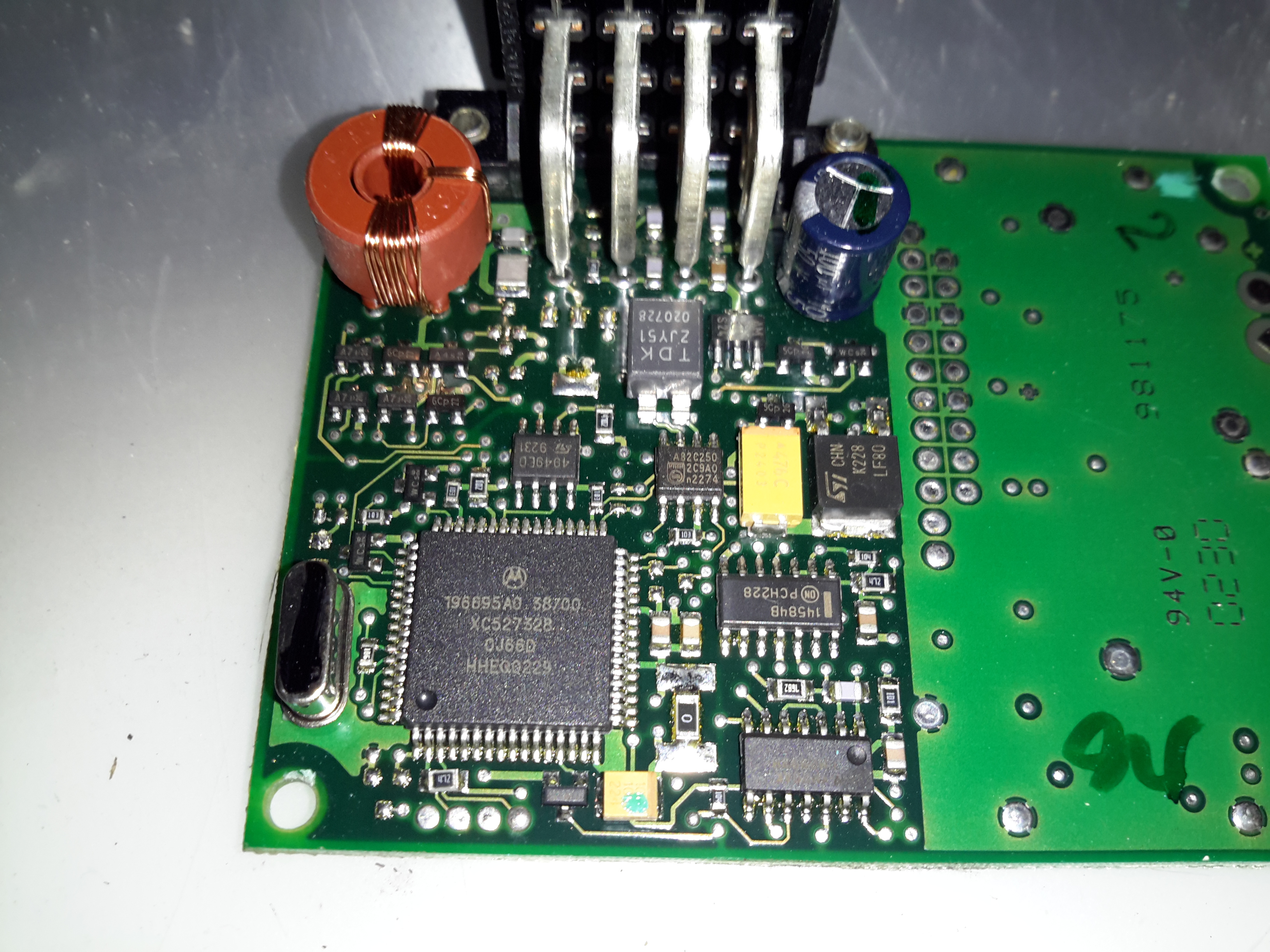
Microcontroller
The large IC from Motorola I’m assuming to be a microcontroller, but I didn’t manage to find anything from the markings. There’s not much else in here apart from some glue logic, and what I think is the 125Khz toroidal antenna in the top left corner.
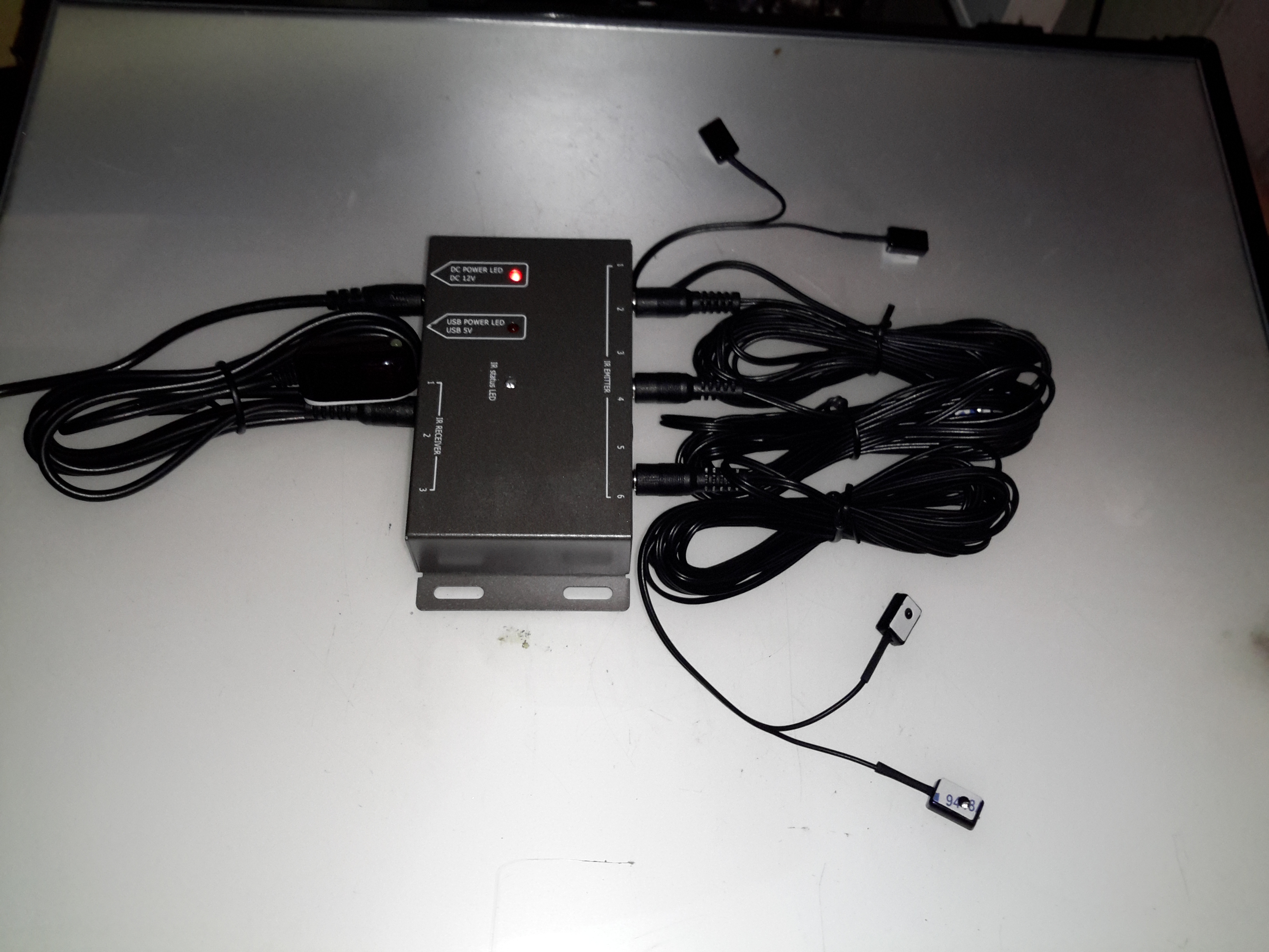
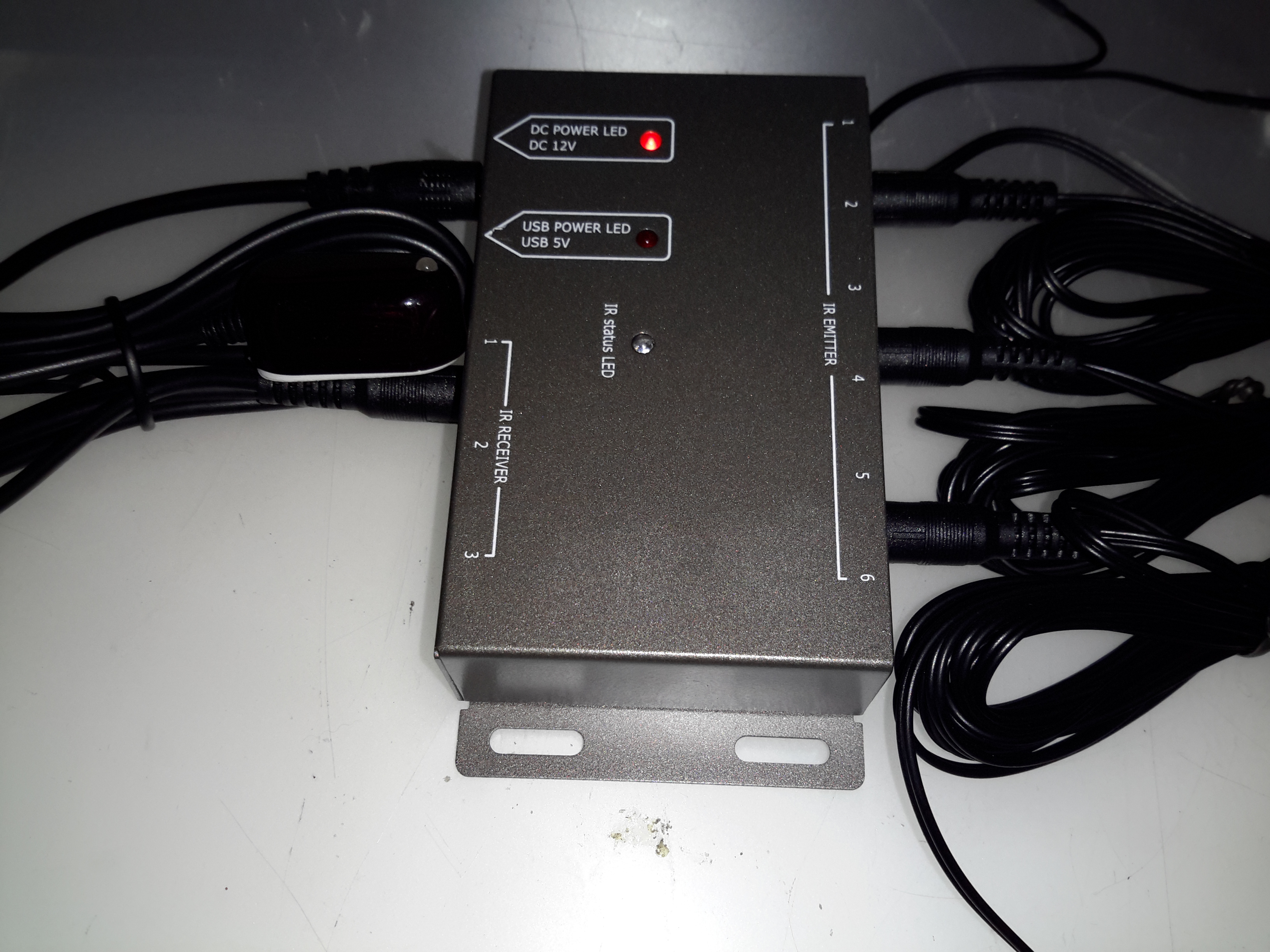
Here’s another random gadget for teardown, this time an IR remote control repeater module. These would be used where you need to operate a DVD player, set top box, etc in another room from the TV that you happen to be watching. An IR receiver sends it’s signal down to the repeater box, which then drives IR LEDs to repeat the signal.
Repeater Module
Not much to day about the exterior of this module, the IR input is on the left, up to 3 receivers can be connected. The outputs are on the right, up to 6 repeater LEDs can be plugged in. Connections are done through standard 3.5mm jacks.
Repeater PCB
Not much inside this one at all, there are 6 transistors which each drive an LED output. This “dumb” configuration keeps things very simple, no signal processing has to be done. Power is either provided by a 12v input, which is fed into a 7805 linear regulator, or direct from USB.
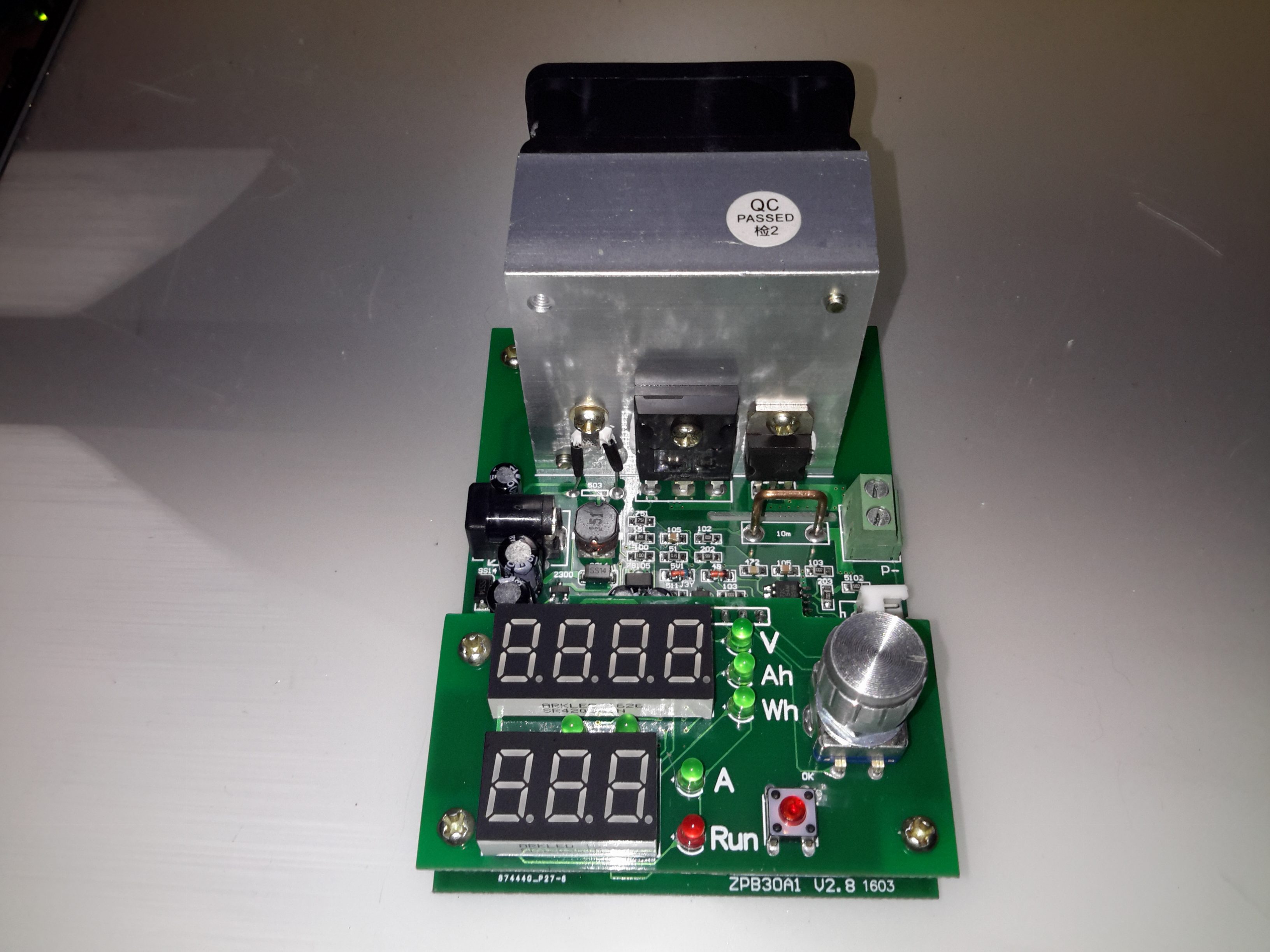
Here’s a useful tool for testing both power supplies & batteries, a dummy load. This unit is rated up to 60W, at voltages from 1v to 25v, current from 200mA to 9.99A.
This device requires a 12v DC power source separate from the load itself, to power the logic circuitry.
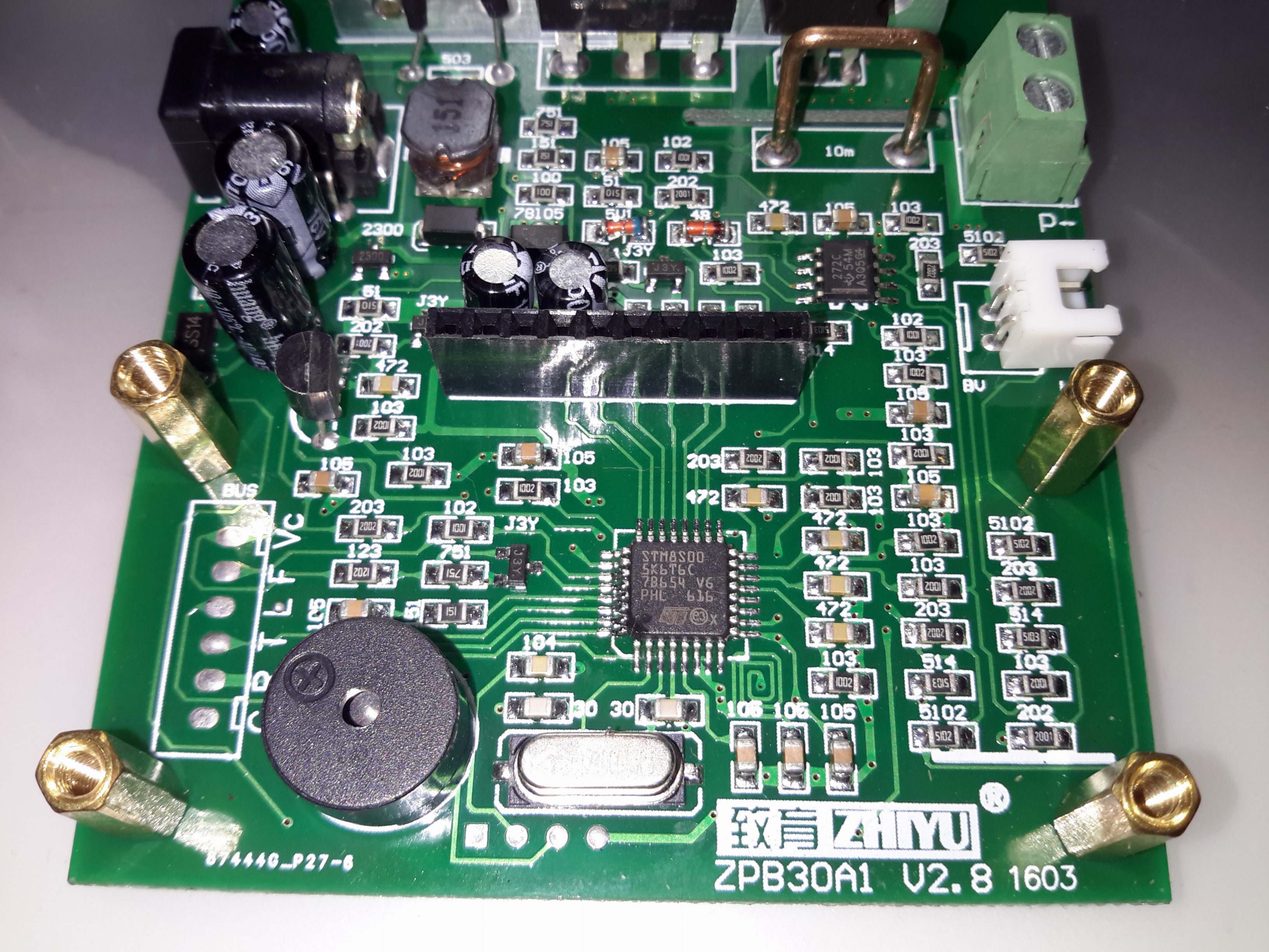
Microcontroller Section
Like many of these modules, the brains of the operation is an STM8 microcontroller. There’s a header to the left with some communication pins, the T pin transmits the voltage when the unit is operating, along with the status via RS232 115200 8N1. This serial signal is only present in DC load mode, the pin is pulled low in battery test mode. The 4 pins underneath the clock crystal are the programming pins for the STM8.
Serial CommsCooling Fan
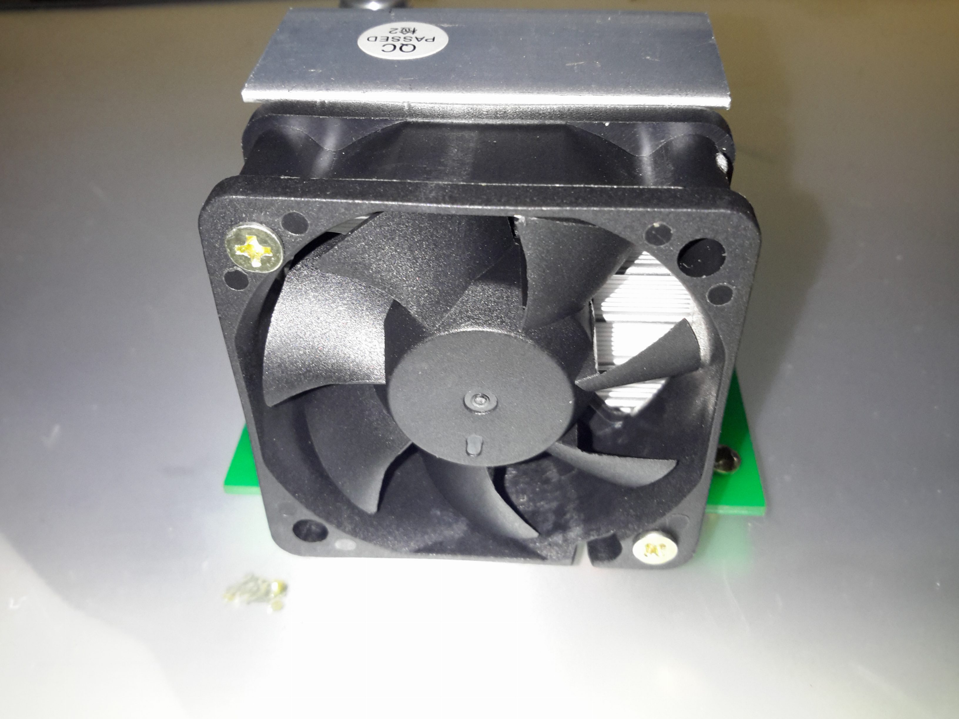
The main heatsink is fan cooled, the speed is PWM controlled via the microcontroller depending on the temperature.
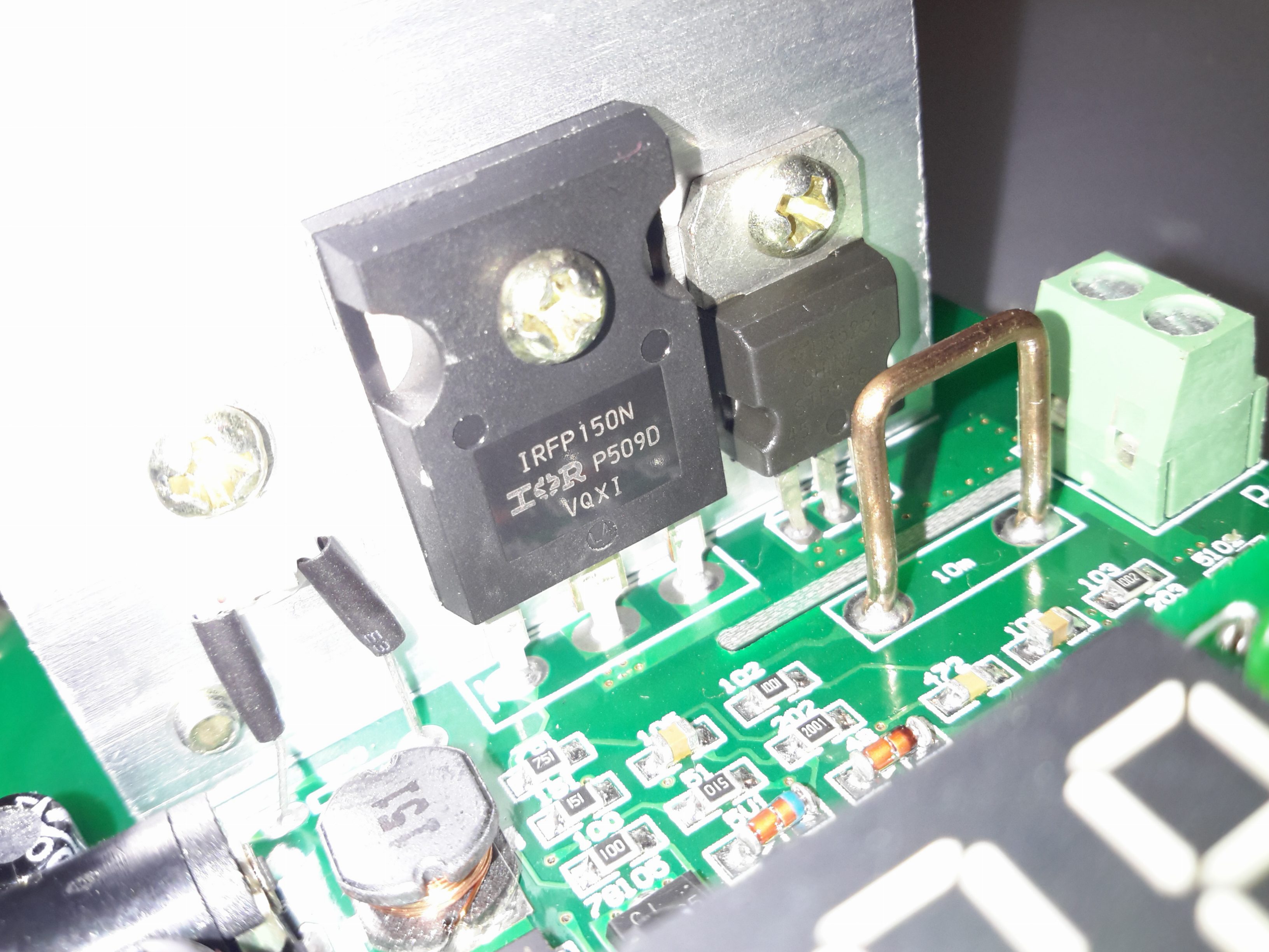
Main MOSFET
The main load MOSFET is an IRFP150N from Infineon. This device is rated at 100v 42A, with a max power dissipation of 160W. On the right is a dual diode for reverse polarity protection, this is in series with the MOSFET. On the left is the thermistor for controlling fan speed.
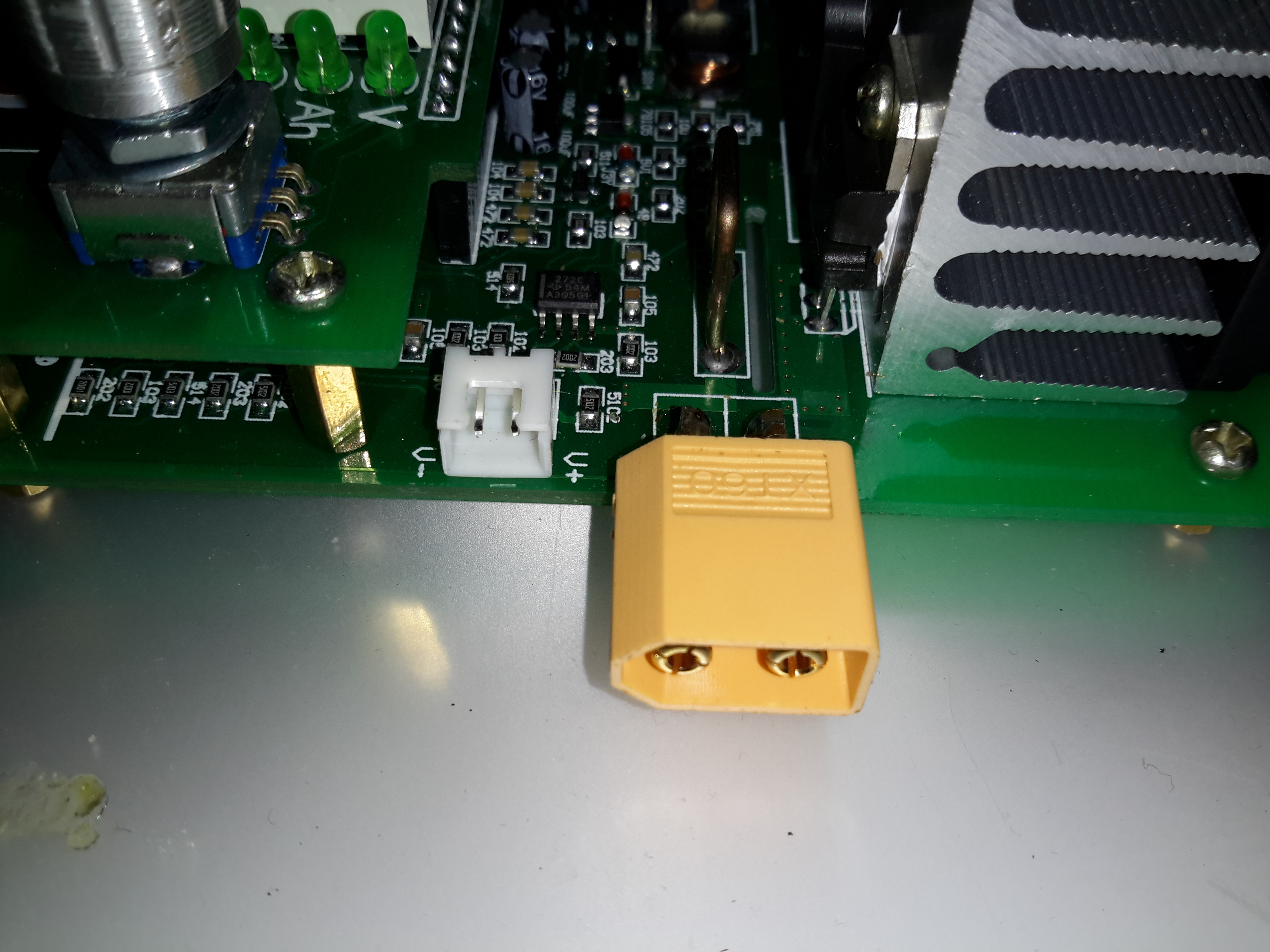
Load Terminals
The load is usually connected via a rising clamp terminal block. I’ve replaced it with a XT60 connector in this case as all my battery holders are fitted with these. This also removes the contact resistance of more connections for an adaptor cable. The small JST XH2 connector on the left is for remote voltage sensing. This is used for 4-wire measurements.
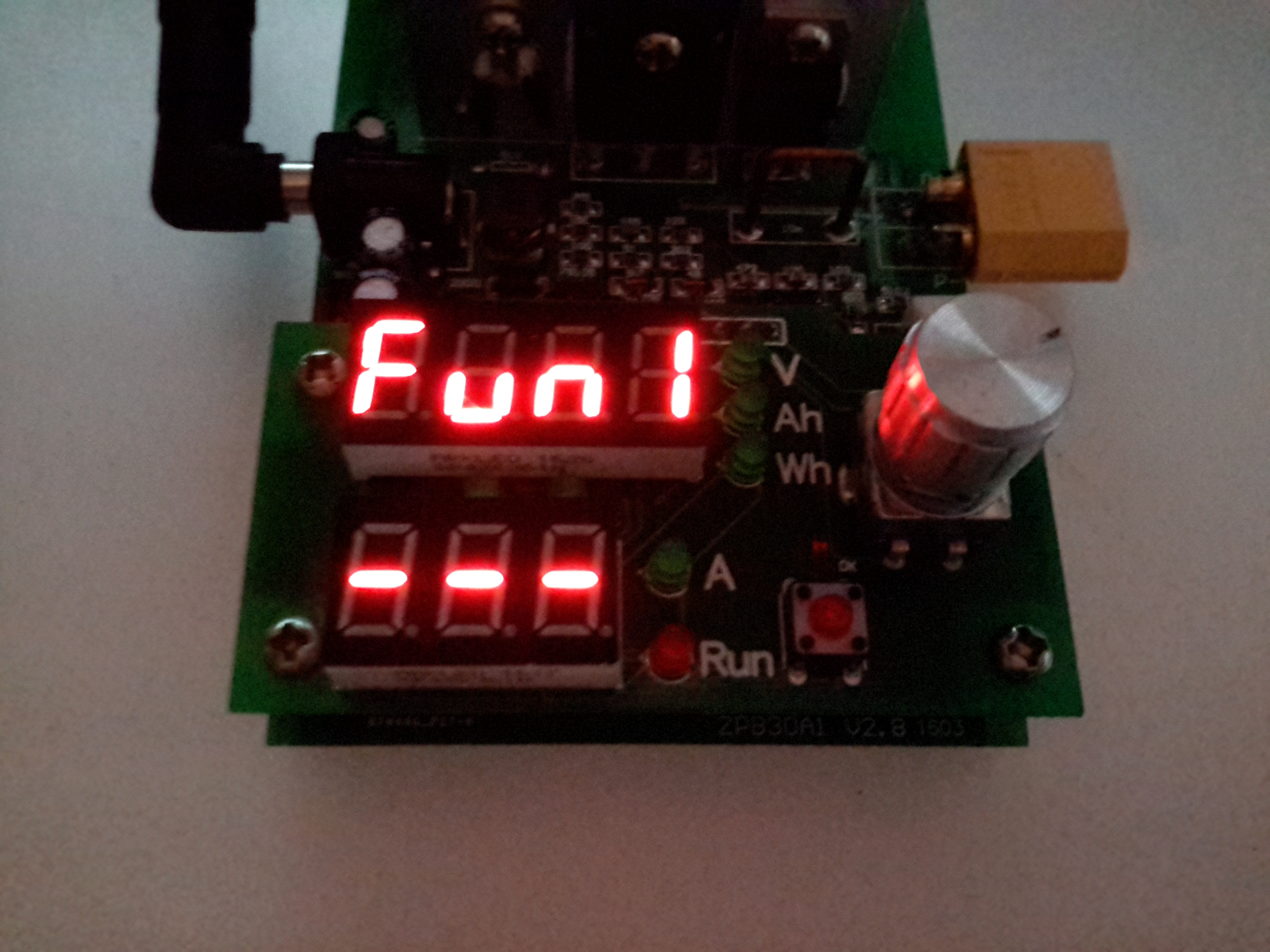
Function 1 – DC Load
Powering the device up while holding the RUN button gets you into the menu to select the operating modes. Function 1 is simple DC load.
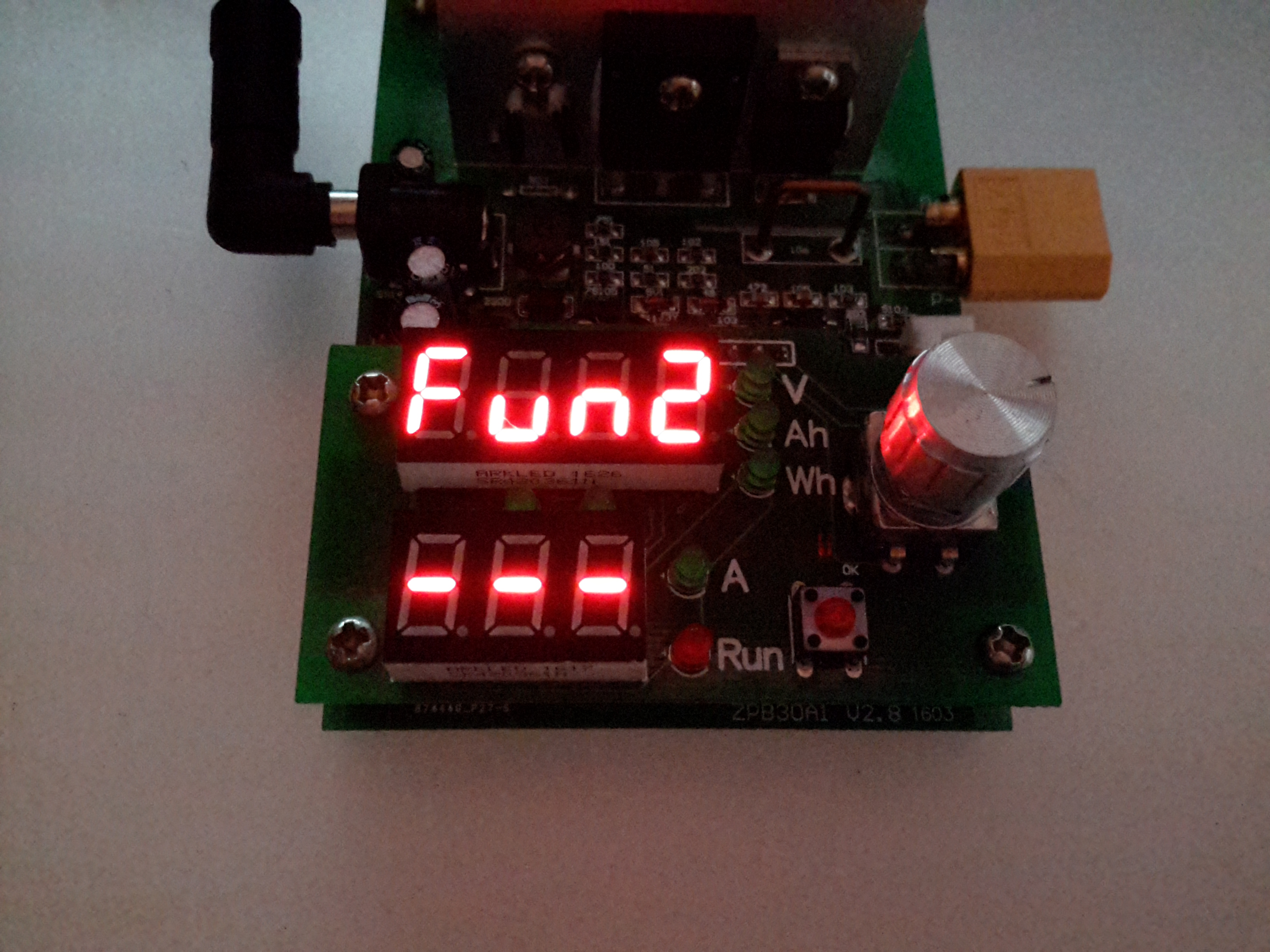
Function 2 – Battery Capacity Mode
The rotary encoder is used to select the option. Function 2 is battery capacity test mode.
Beeper Mode
After the mode is selected, an option appears to either turn the beeper on or off.
Amps Set
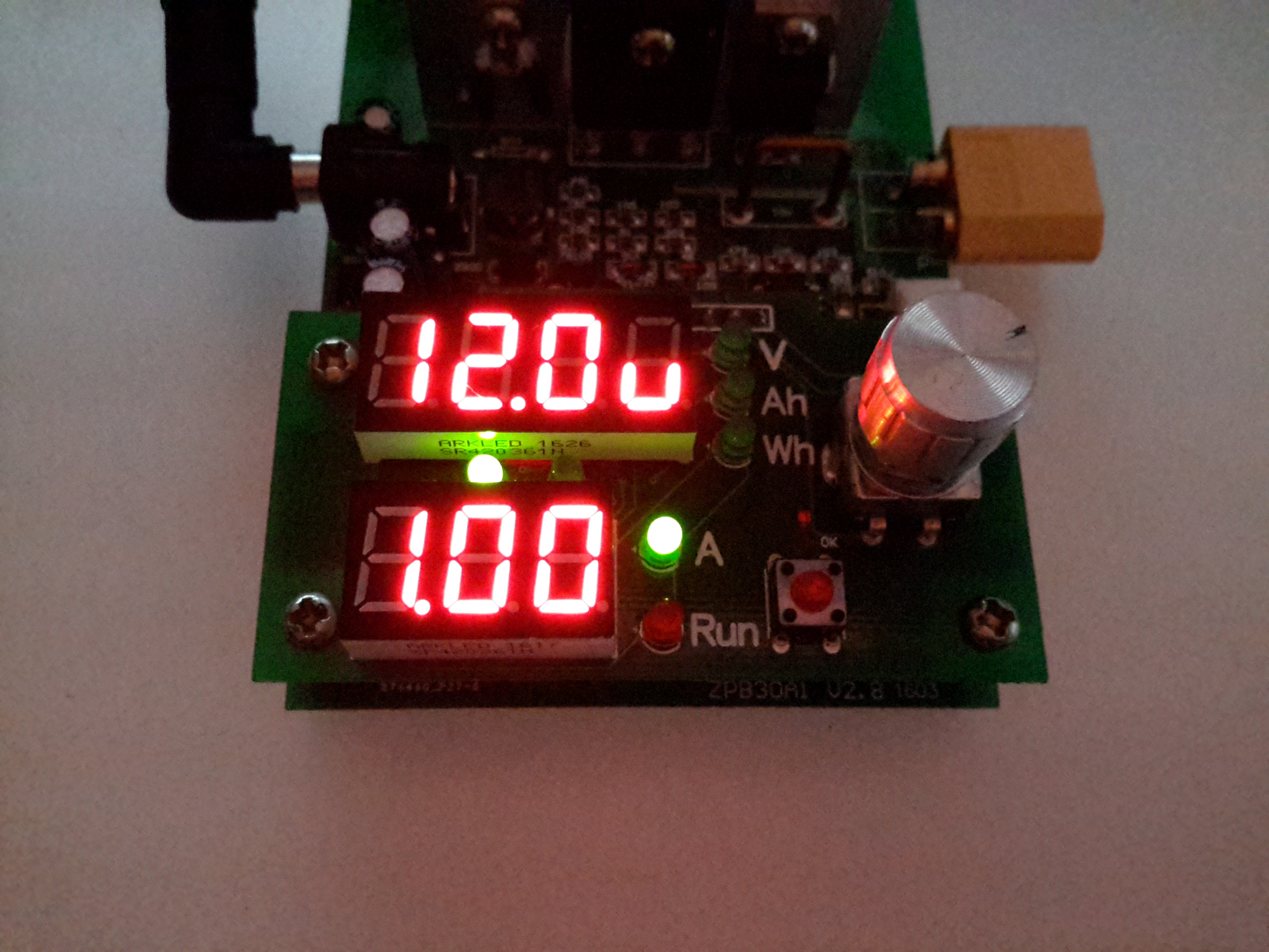
When in standby mode, the threshold voltage & the load current can be set. Here the Amps LED is lit, so the load current can be set. The pair of LEDs between the displays shows which digit will be changed. Pressing the encoder button cycles through the options.
Volts Set
With the Volts LED lit, the threshold voltage can be changed.
When in DC load mode (Fun1), the device will place a fixed load onto the power source until it’s manually stopped. The voltage setting in this mode is a low-voltage alarm. The current can be changed while the load is running.
When in battery discharge test mode (Fun2), the voltage set is the cutoff voltage – discharge will stop when this is reached. Like the DC load mode, the current can be changed when the load is running. After the battery has completed discharging, the capacity in Ah & Wh will be displayed on the top 7-segment. These results can be selected between with the encoder.
Below are tables with all the options for the unit, along with the error codes I’ve been able to decipher from the Chinese info available in various places online. (If anyone knows better, do let me know!).
Option
Function
Fun1
Basic DC Load
Fun 2
Battery Capacity Test
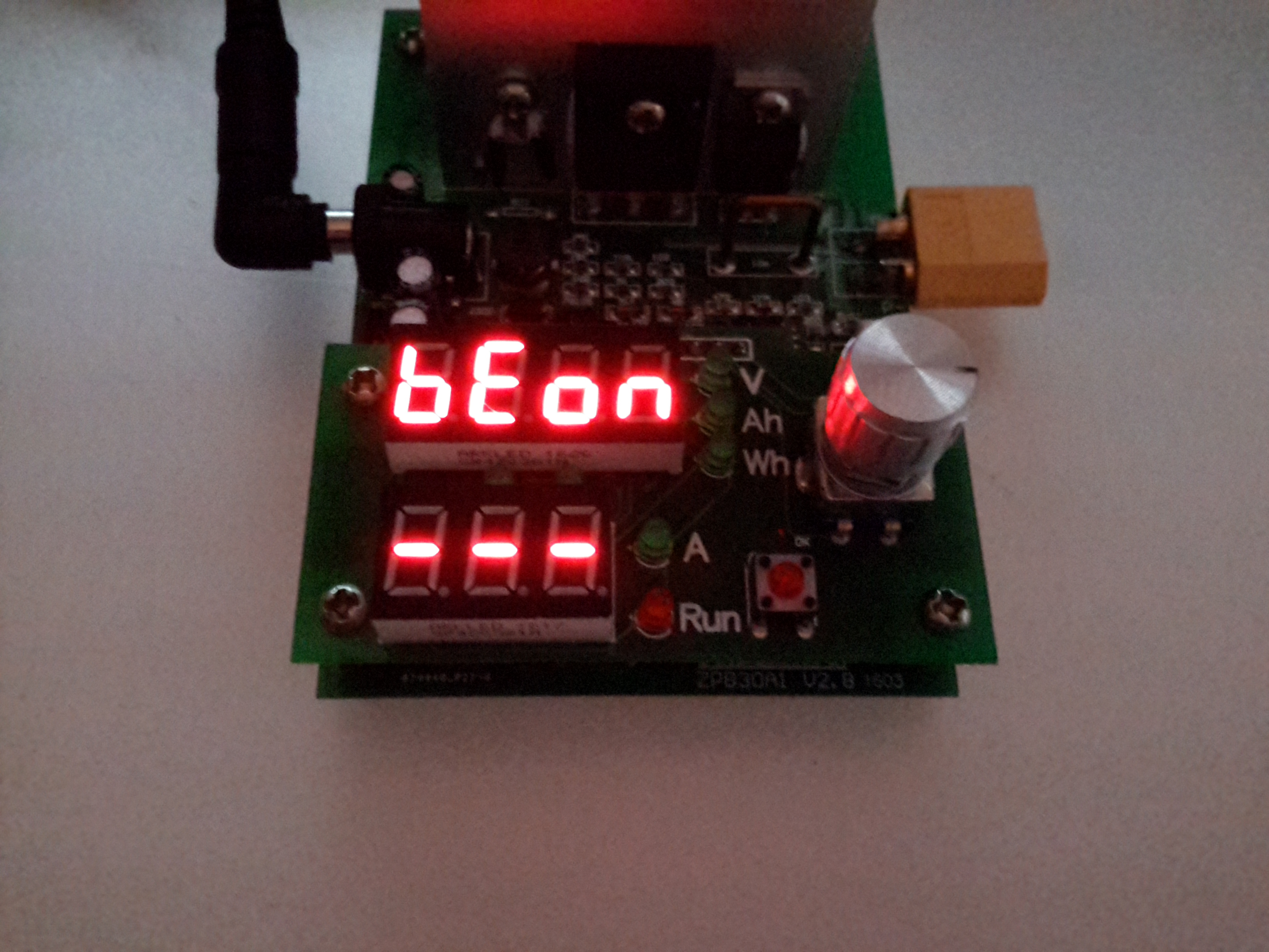
BeOn
Beeper On
BeOf
Beeper Off
Error Code
Meaning
Err1
Input Overvoltage
Err2
Low Battery Voltage / No Battery Present / Reverse Polarity
Err3
Battery ESR Too High / Cannot sustain selected discharge current
Err4
General Failure
Err6
Power Supply Voltage Too Low / Too High. Minimum 12v 0.5A.
I was recently given a pretty nice LED backlit 1080p LG monitor, with the instruction that it wouldn’t power on correctly. The monitor would power on as far as the standby light, but when fully powered on, would flash the backlight momentarily then shut down. A power supply issue was immediately suspected.
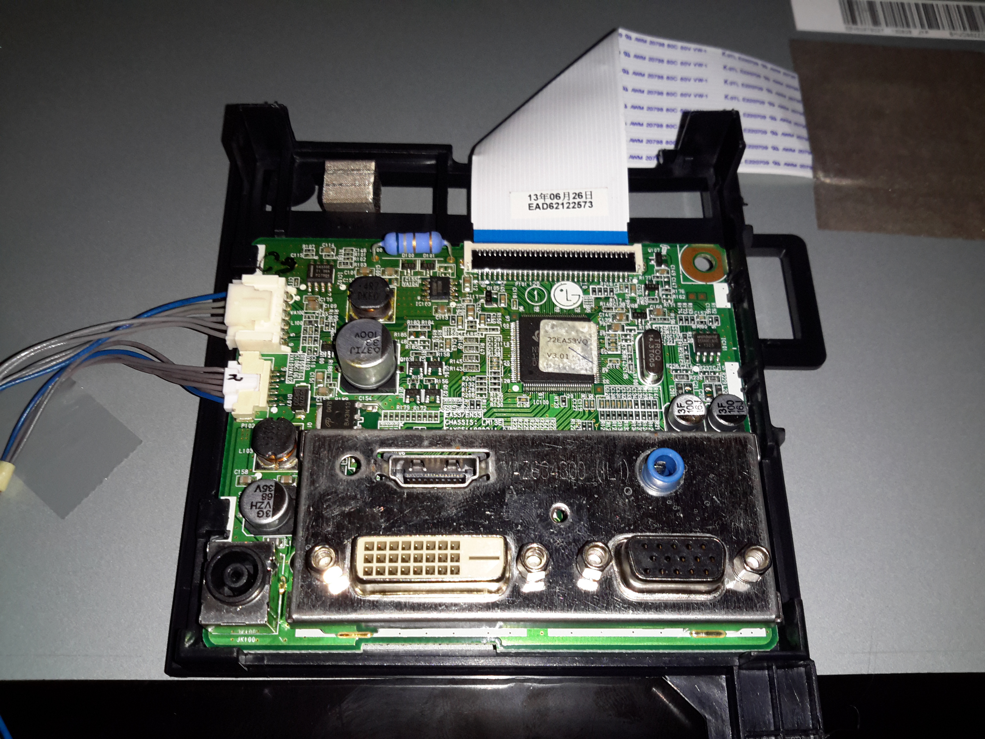
LCD Logic Board
I popped the covers off the monitor itself first, thinking that it was an electrolytic gone bad in the backlight DC-DC converter. Not to mention the fact that cracking into a wall-wart type of PSU is only occasionally possible without the use of anger & large hammers. (Cracking the glue with the handle of a screwdriver doesn’t work so well when the factory went a bit nuts with the glue/ultrasonic welder). As can be seen in the photo, there’s not much inside these monitors, the logic is a single-chip solution, the rest of the PCB is dedicated to supplying the power rails for the various circuits. On the left is the power input & the DC-DC converter for the backlight, along with the DC-DC converter supplying the logic circuits. None of the capacitors here are damaged, everything looks good.
I then measured the output of the PSU, which under no load was the correct 19v DC. However applying any load caused the output voltage to drop like a proverbial brick. Applying a full load of 1.3A saw the output voltage drop so severely that the PSU tripped on it’s UVLO.
200mA Load
At 200mA of load the factory PSU is already dropping to 18v, with a 5.3kHz switching frequency appearing.
500mA Load
At higher load the frequency increases to 11.5kHz & the output voltage has dropped to 11.86v!
750mA Load
750mA was as high as I could make the supply go without it tripping itself out – the UVLO circuit trips at 9v. 12.6kHz is now riding on the severely low DC at this point.
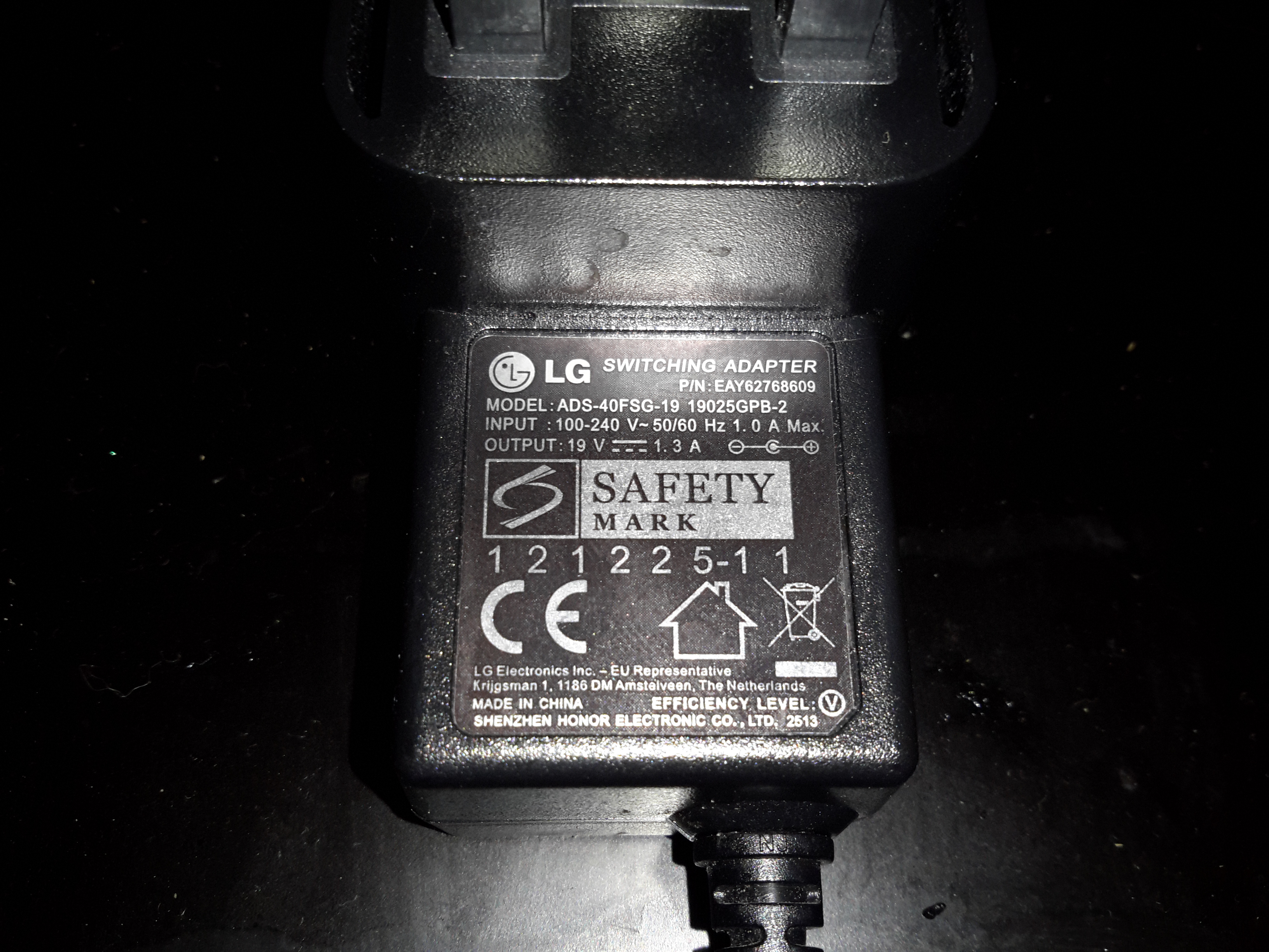
PSU Ratings
The power supply is supposed to be rated at 1.3A at 19v, however with this fault it’s getting nowhere near that. The LG brand is on this PSU but it’s contracted out to Shenzen Honor Electric Co. Ltd.
Output Electrolytic
Here’s the problem with this PSU. The output electrolytic has ballooned. I don’t have an ESR tester, but this cap has gone way past it’s sell-by date. It’s position right next to the heatsink with the output rectifier diodes has probably cooked it. The PSU isn’t that badly built for a Chinese one – there’s plenty of creepage distance on the PCB & even a couple of isolation slots.
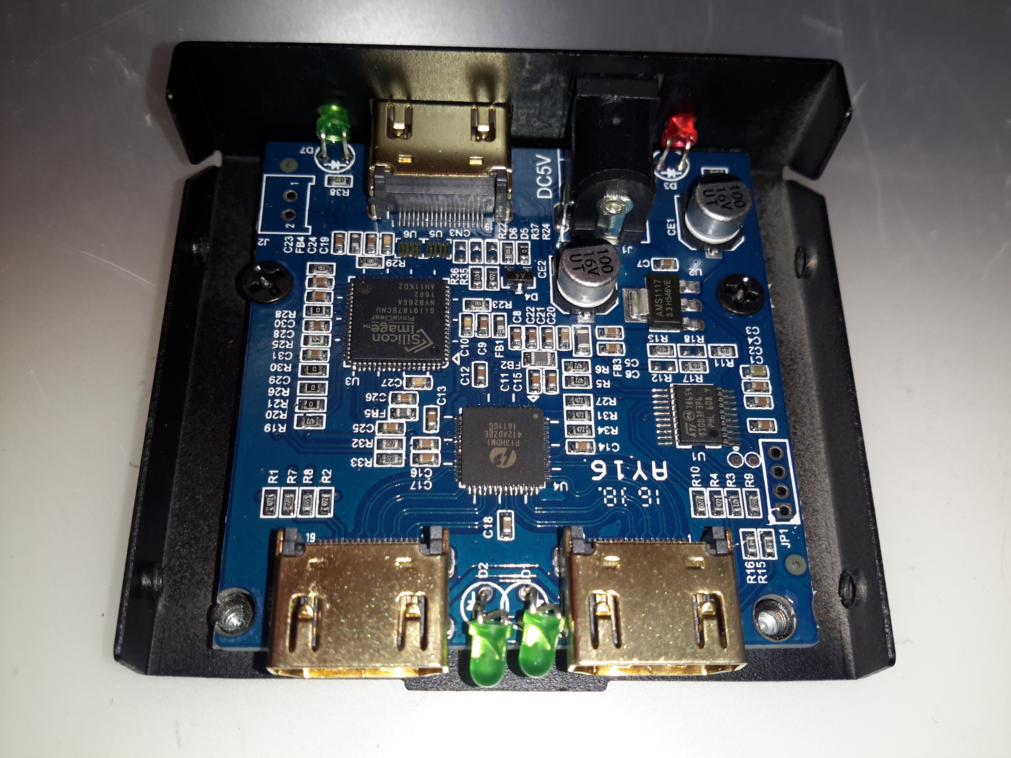
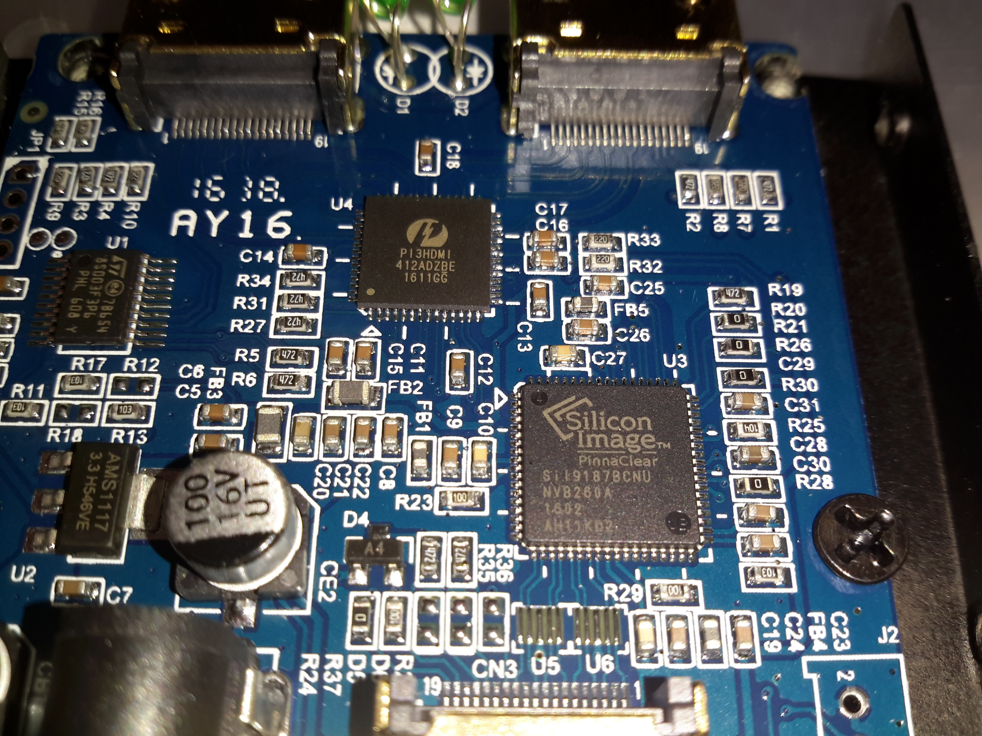
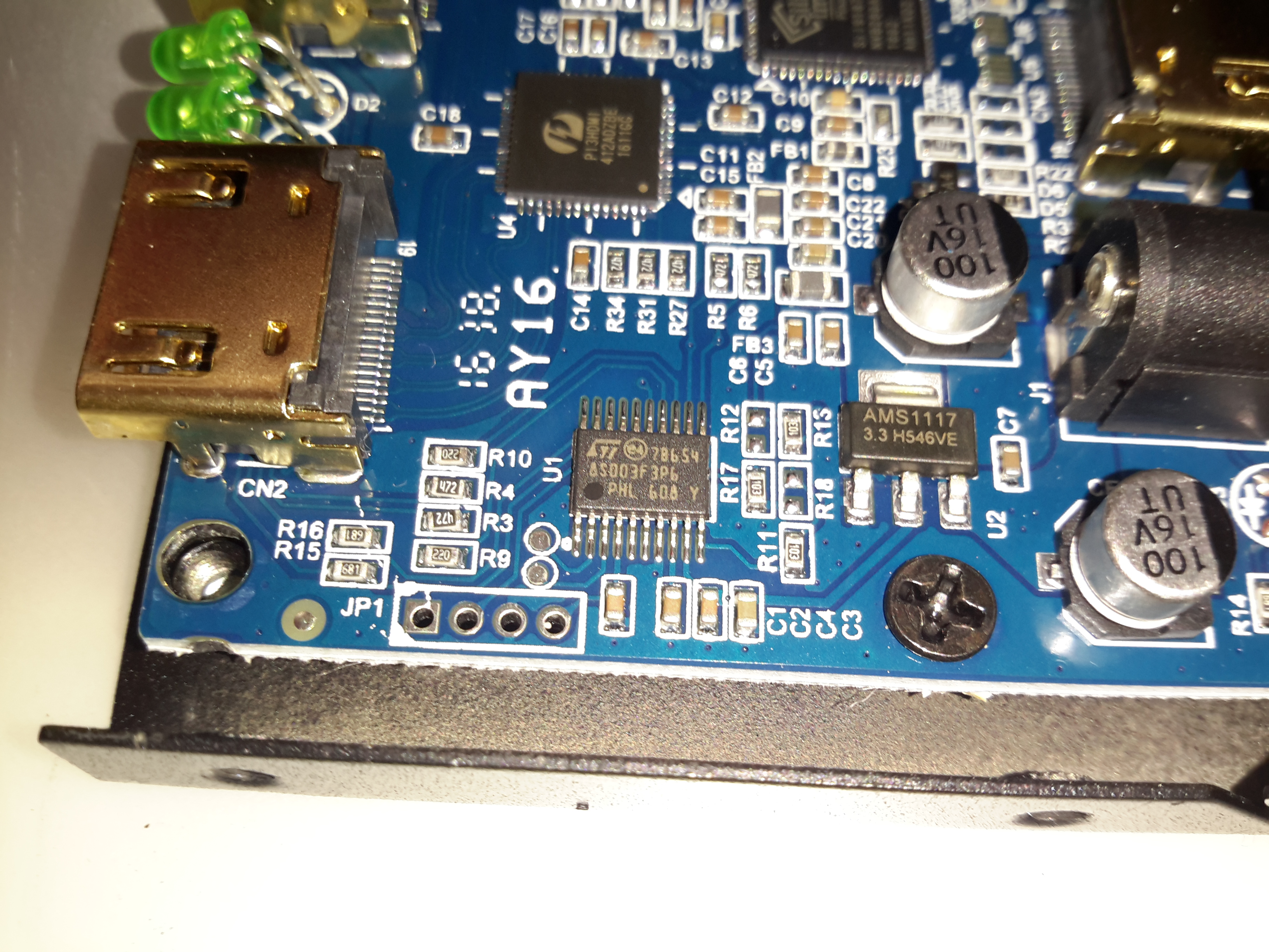
Time for another random teardown, a signal splitter for HDMI. These units are available very cheap these days on eBay. This one splits the incoming signal into two to drive more than one display from the same signal source.
Main PCB
The stamped alloy casing comes apart easily with the removal of a few screws. The PCB inside is rather densely packed with components.
Chipset
The main IC on the incoming signal is a Silicon Image Sil9187B HDMI Port Processor, with a single input & 4 outputs. In this case the chip is used as a repeater to amplify the incoming signal. the signal path then gets fed into a Pericom PI3HDMI412 HDMI Demux, which then splits the signal into two for the output ports.
Microcontroller
The main pair of ICs processing the video signals are controlled over I²C, with this STM32 microcontroller. The 4 pads to the lower left are for the STLink programmer. The main 3.3v power rail is provided by the LM1117 linear regulator on the right.
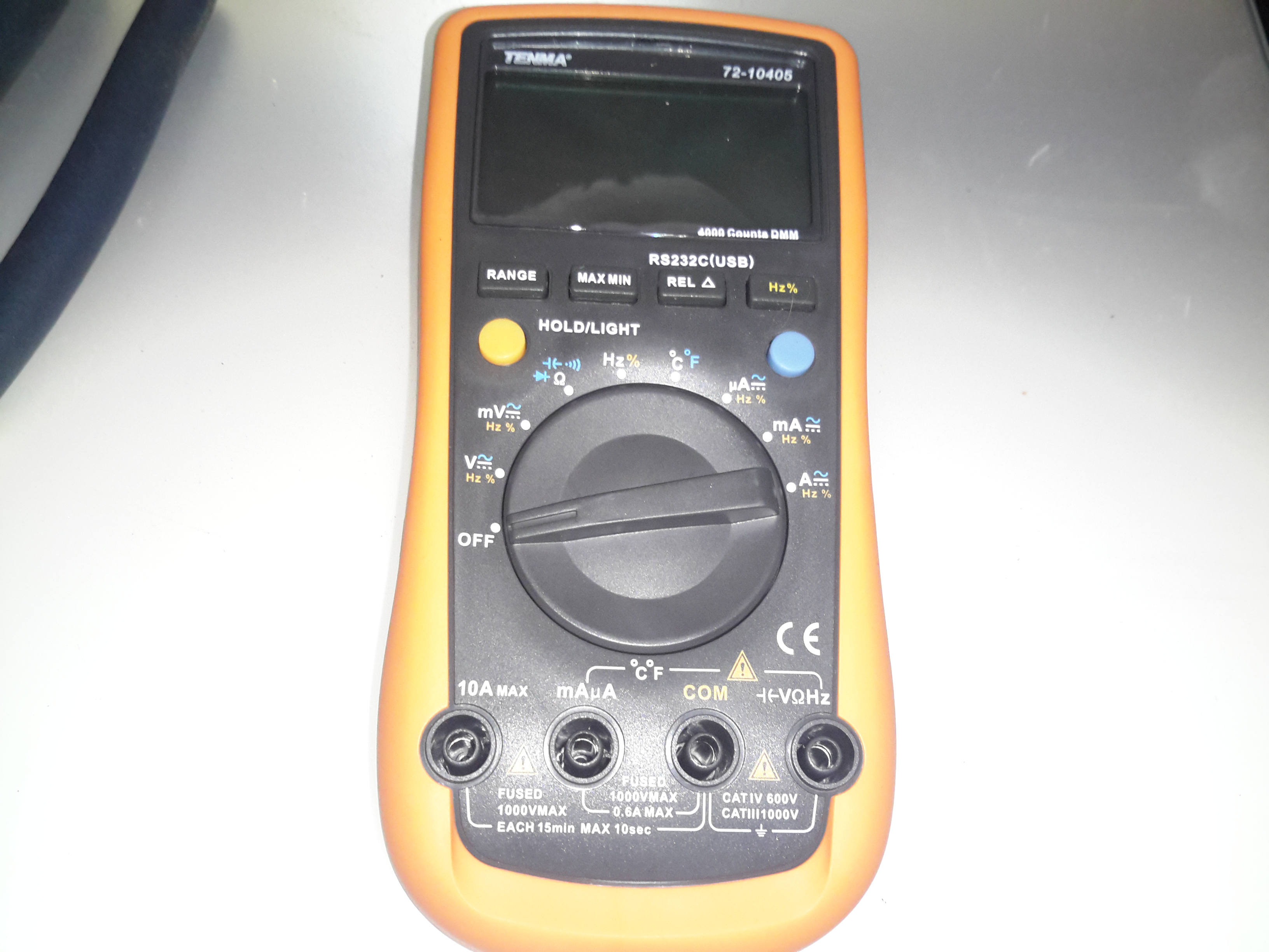
Well it’s time for a new DMM. After the last pair of eBay El-Cheapo Chinese meters just didn’t last very well, I decided a proper meter was required. This one is a Tenma 72-10405, stocked by Farnell for under £60. Not quite as many festures as the cheapo Chinese meters, but I expect this one to be a bit more reliable.
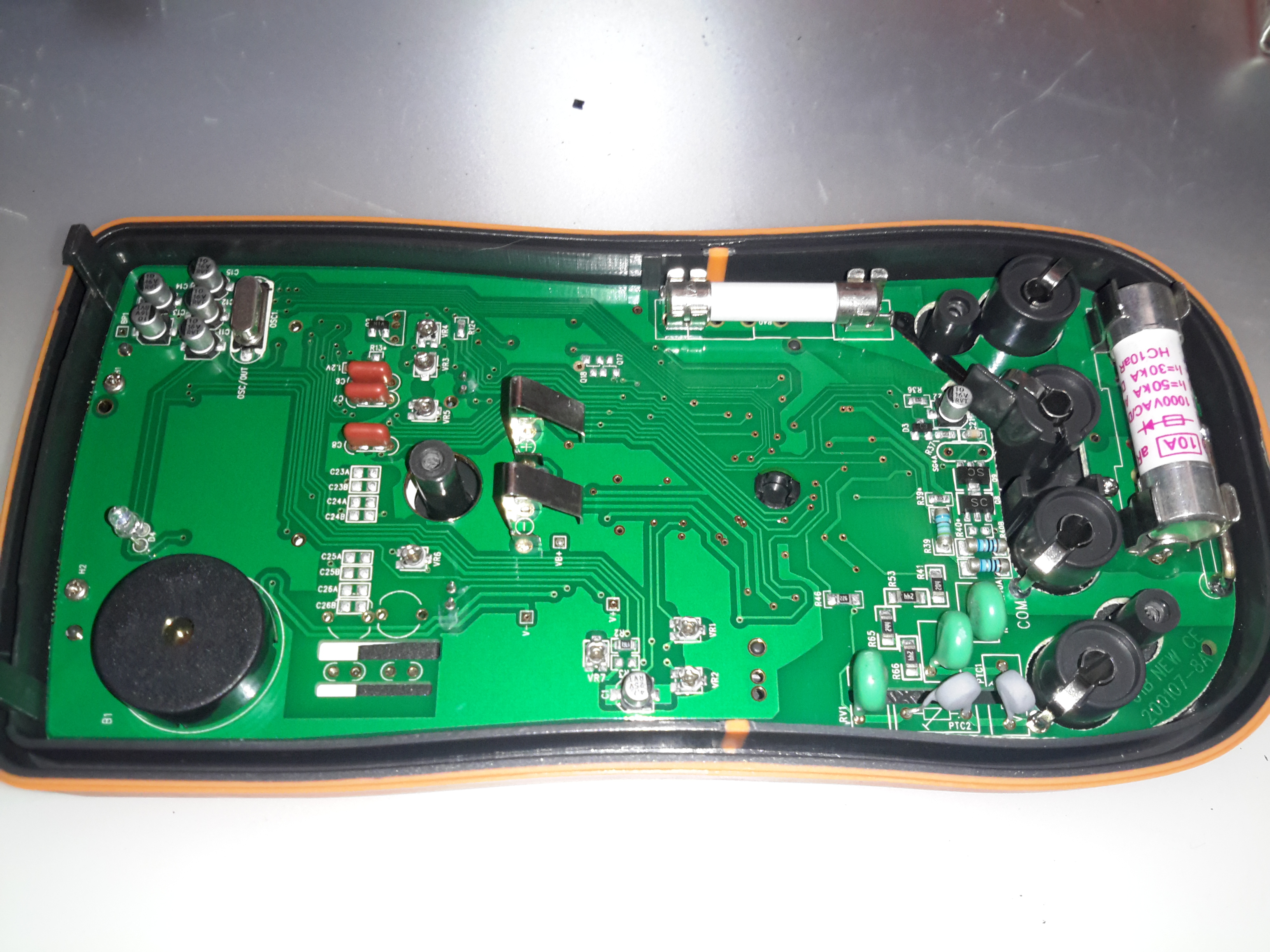
PCB Rear
Since I can’t have anything without seeing how it’s put together, here’s the inside of the DMM. (Fuse access is only possible by taking the back cover off as well. The 9v PP3 battery has a seperate cover).
PCB Rear Bottom
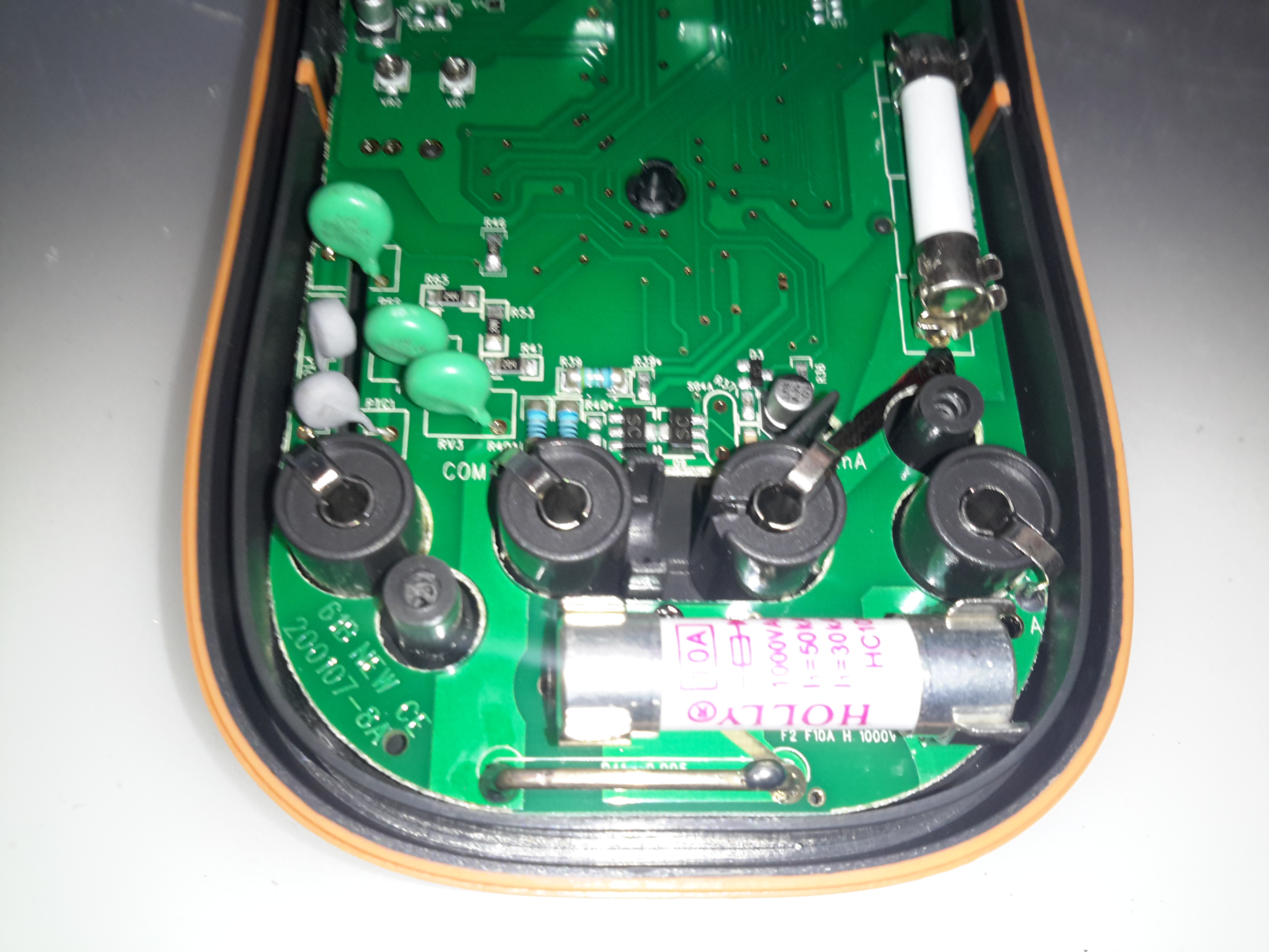
He’s the input section of the meter, with the 10A HRC fuse & current shunt for the high-amps range. The other fuse above is for the mA/µA ranges. The back cover has a wide lip around the edge, that slots into a recess in the front cover, presumably for blast protection if the meter should meet a sticky end. The HRC fuses are a definite improvement over the cheap DMMs, they only have 15mm glass fuses, and no blast protection built into the casing.
There are some MOVs for input protection on the volts/ohms jack, the jacks themselves are nothing more than stampings though.
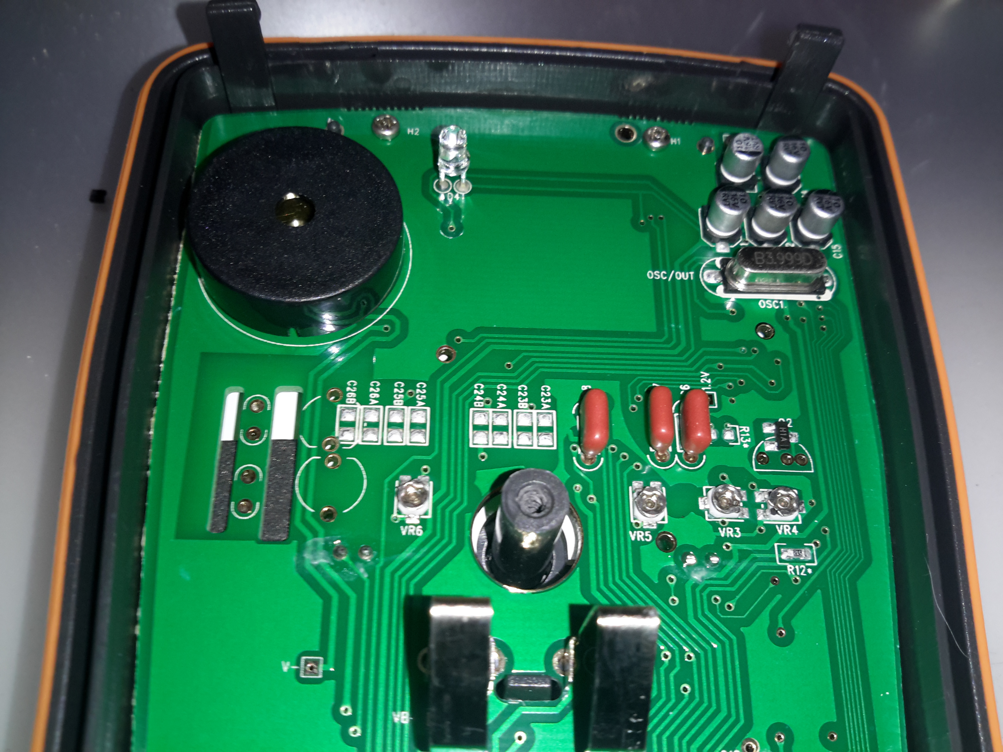
PCB Rear Top
Not much at the other side of the board, there’s the IR LED for the RS232 interface & the beeper.
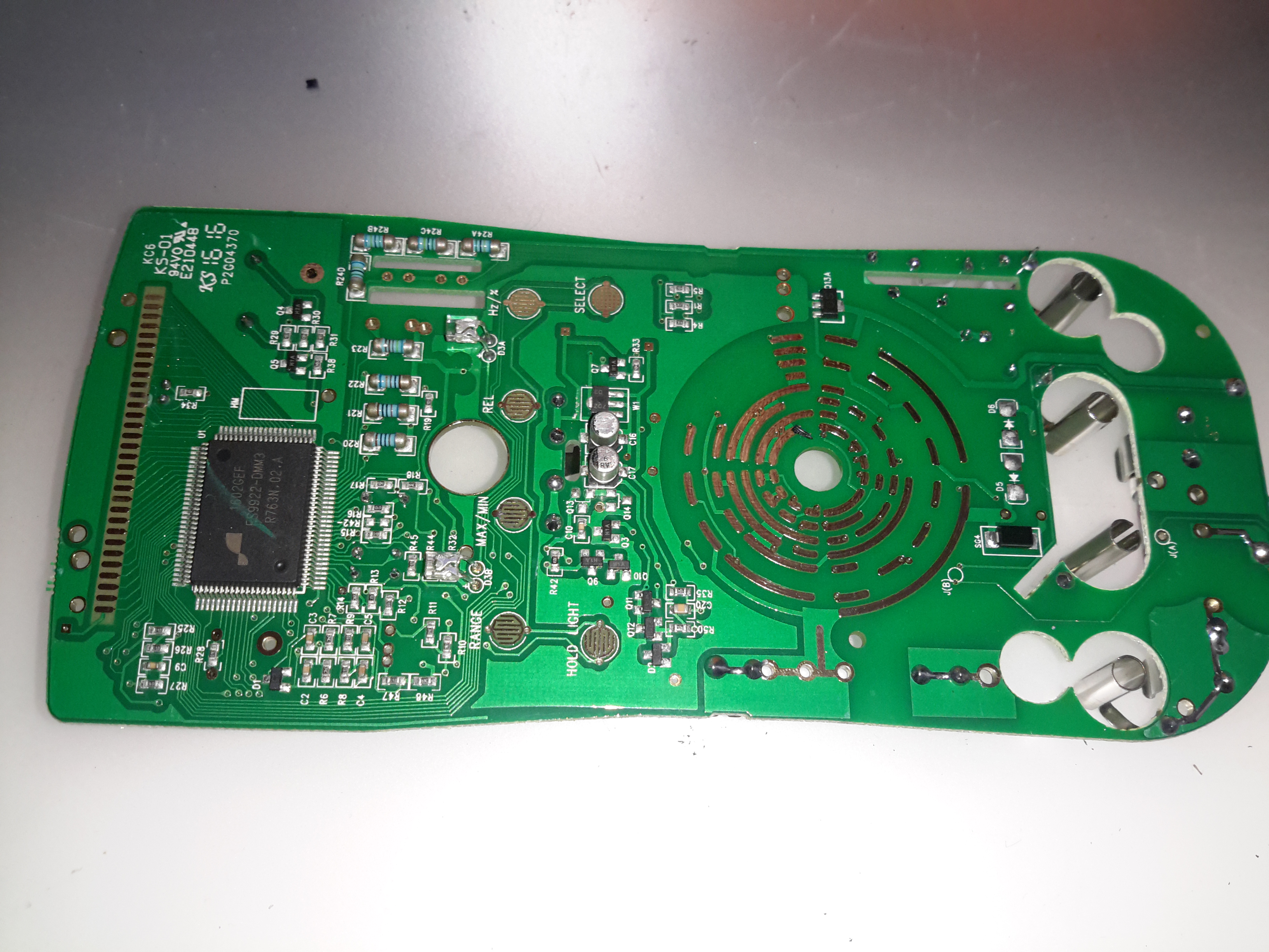
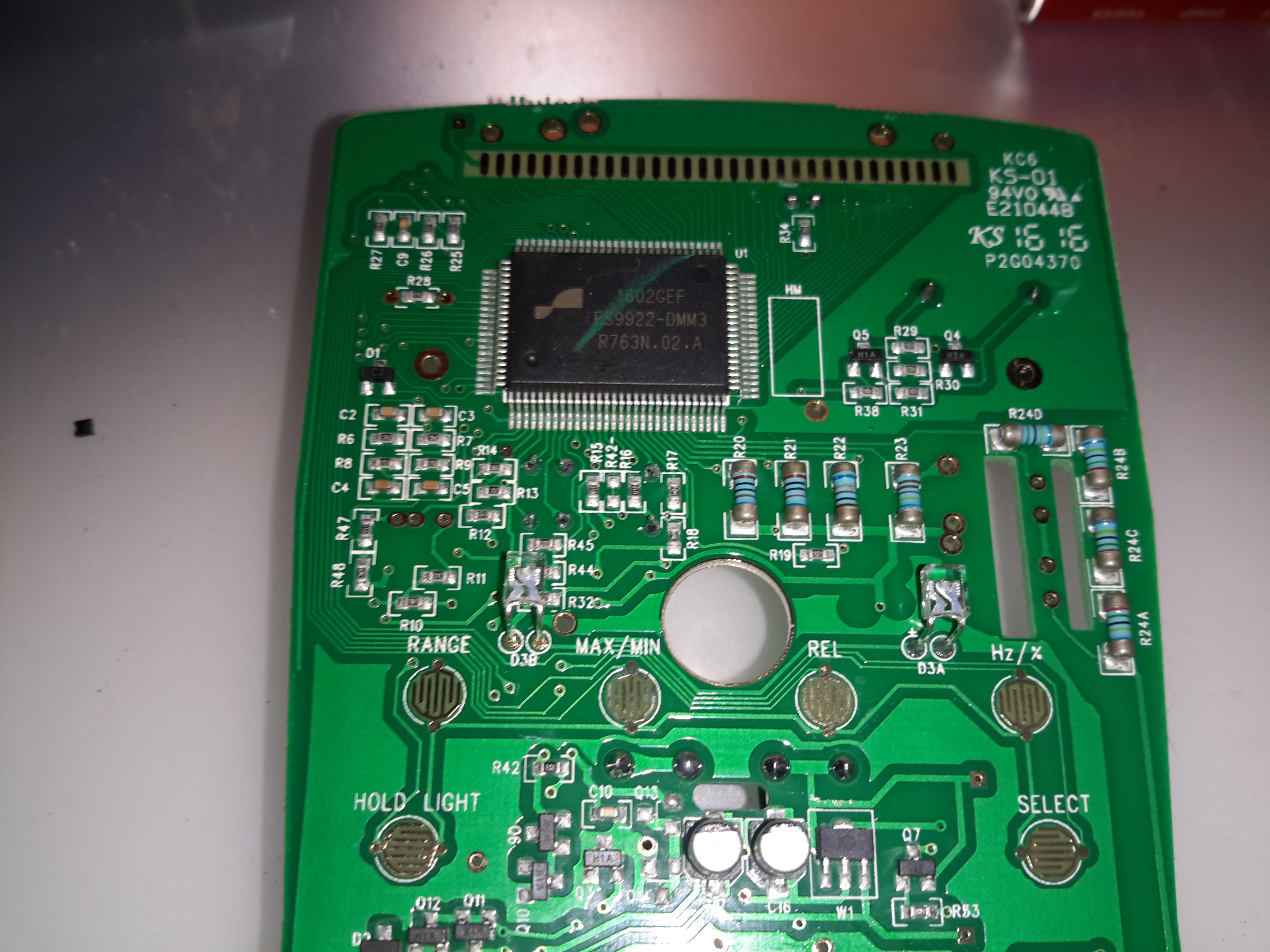
PCB Front
Most of the other components are on the other side of the PCB under the LCD display. The range switch is in the centre, while the main chipset is on the left.
DMM Chipset
The chipset of this meter is a FS9922-DMM3 from Fortune Semiconductor, this is a dedicated DMM chipset with built in ADCs & microcontroller.
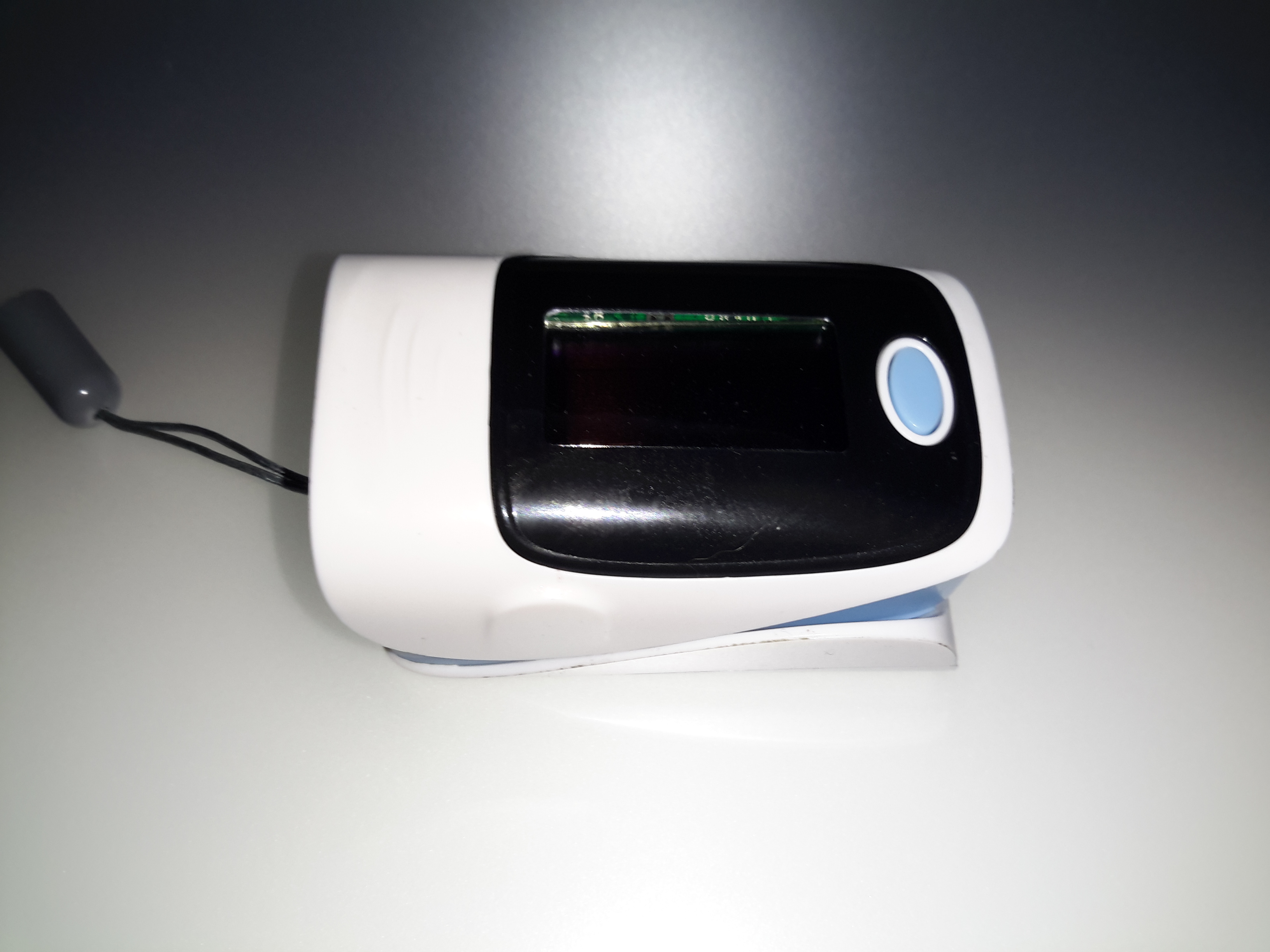
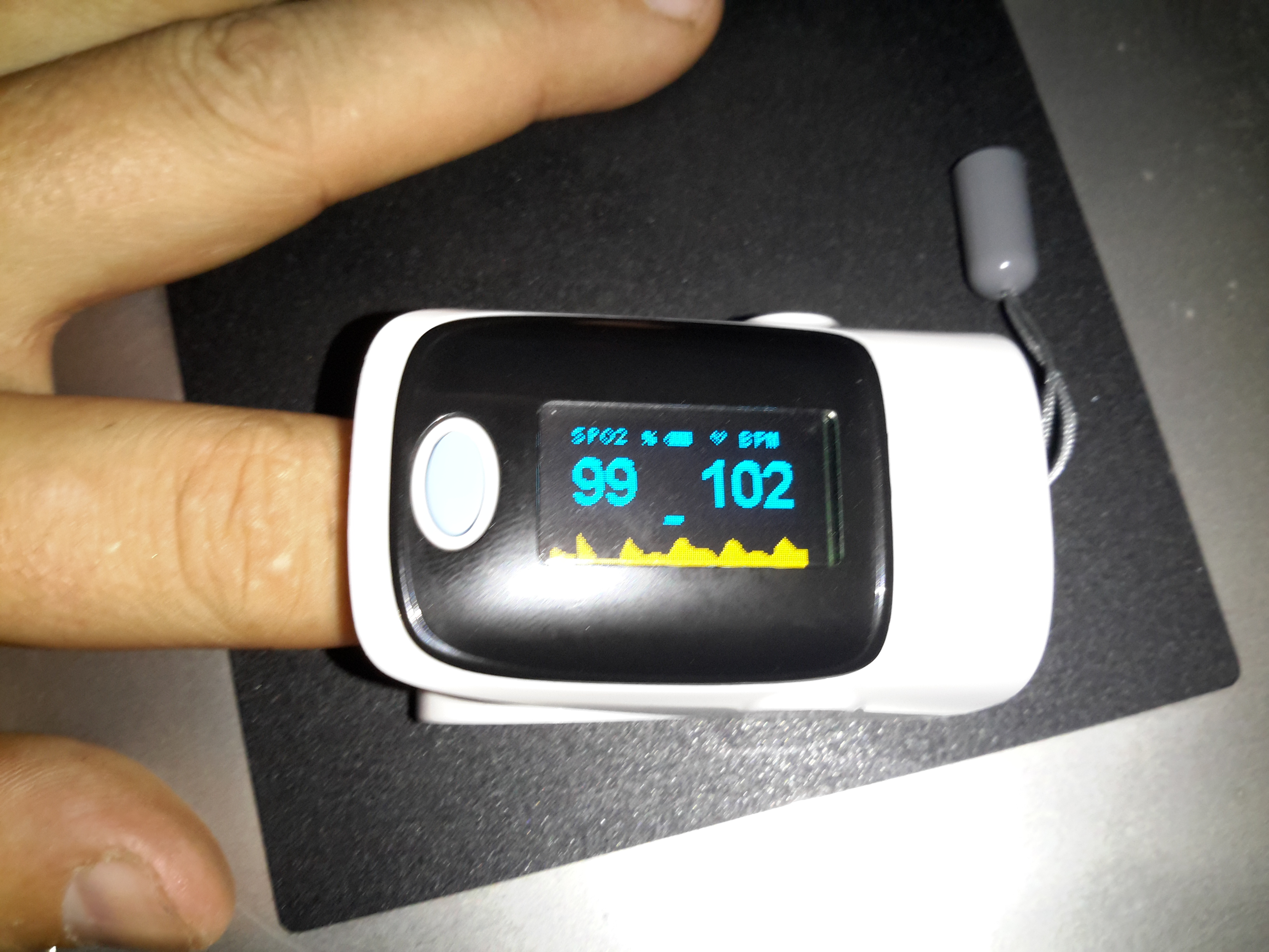
Here’s a piece of medical equipment that in recent years has become extremely cheap, – a Pulse Oximeter, used to determine the oxygen saturation in the blood. These can be had on eBay for less than £15.
Powered On
This one has a dual colour OLED display, a single button for powering on & adjusting a few settings. These cheap Oximeters do have a bit of a cheap plastic feel to them, but they do seem to work pretty well.
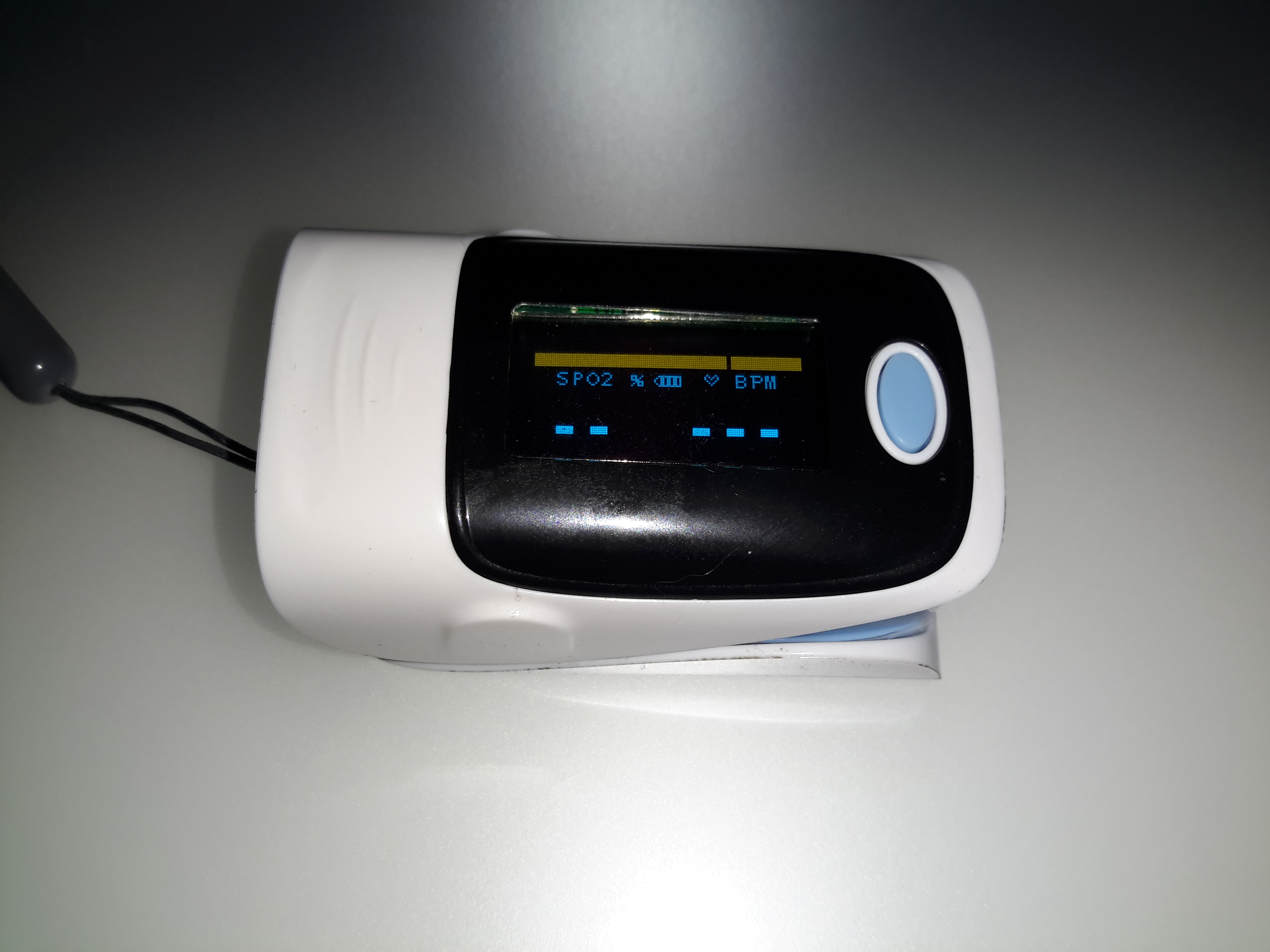
Pulse Oximeter
After a few seconds of being applied to a finger, the unit gives readings that apparently confirm that I’m alive at least. 😉 The device takes a few seconds to get a baseline reading & calibrate the sensor levels.
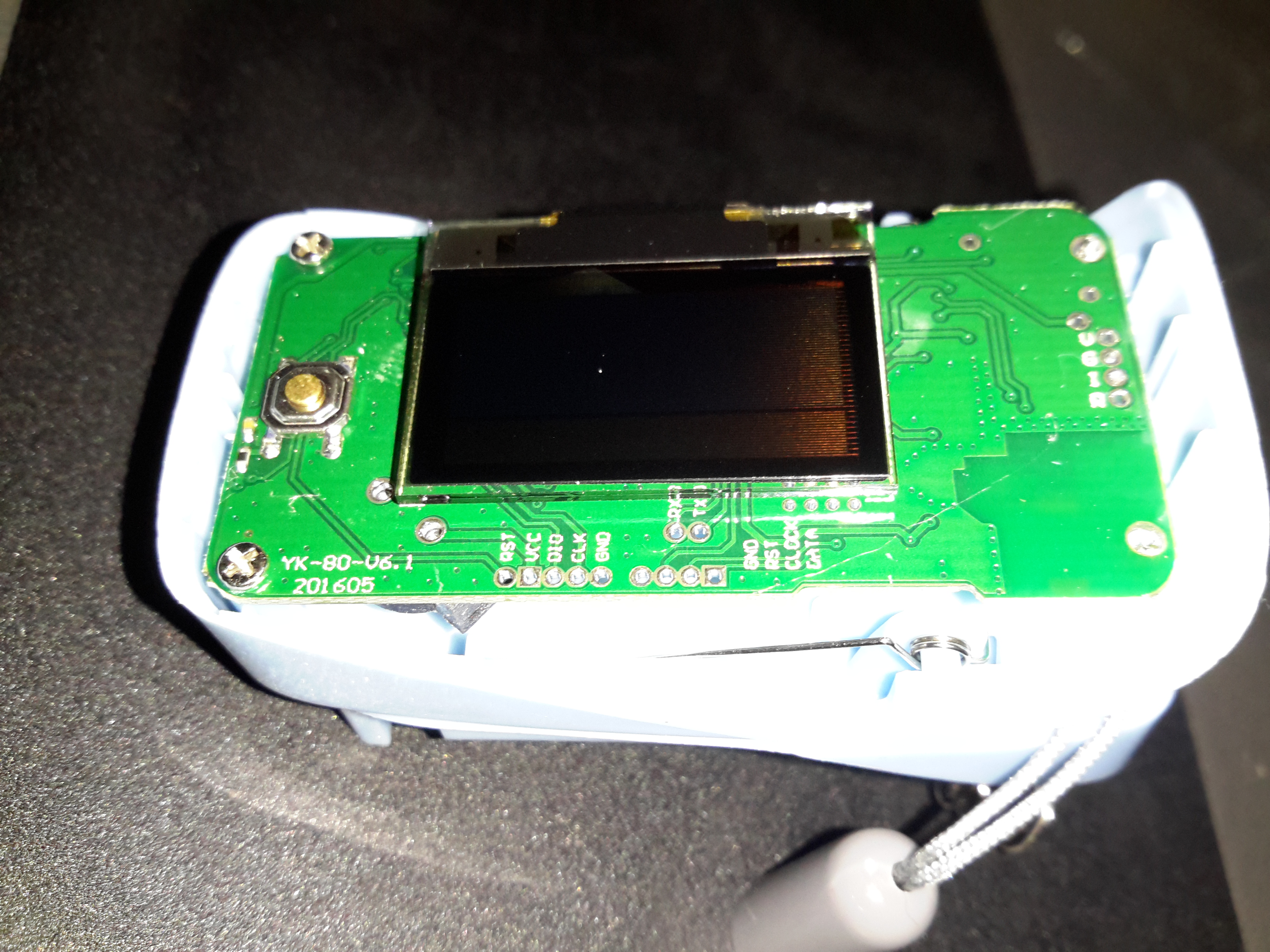
Main PCB Top
The plastic casing is held together with a few very small screws, but comes apart easily. here is the top of the main board with the OLED display panel. There appears to be a programming header & a serial port on the board as well. I’ll have to poke at these pads with a scope to see if any useful data is on the pins.
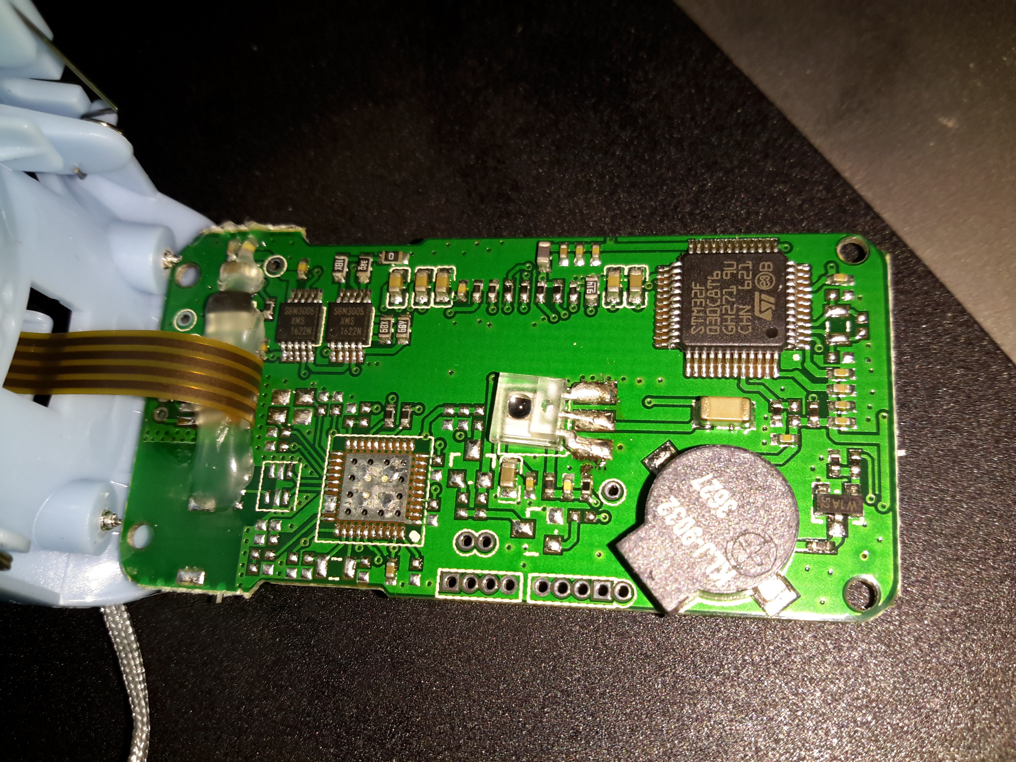
Main PCB Bottom
The bottom of the board has all the main components of the system. The microcontroller is a STM32F03C8T6, these are very common in Chinese gear these days. There’s a small piezo beeper & the main photodiode detector is in the centre.
There is an unpopulated IC space on the board with room for support components. I suspect this would be for a Bluetooth radio, as there’s a space at the bottom left of the PCB with no copper planes – this looks like an antenna mounting point. (The serial port on the pads is probably routed here, for remote monitoring).
At the top left are a pair of SGM3005 Dual SPDT analogue switches. These will be used to alternate the red & IR LEDs on the other side of the shell.
A 4-core FFC goes off to the other side of the shell, bringing power from the battery & supplying the sensing LEDs.
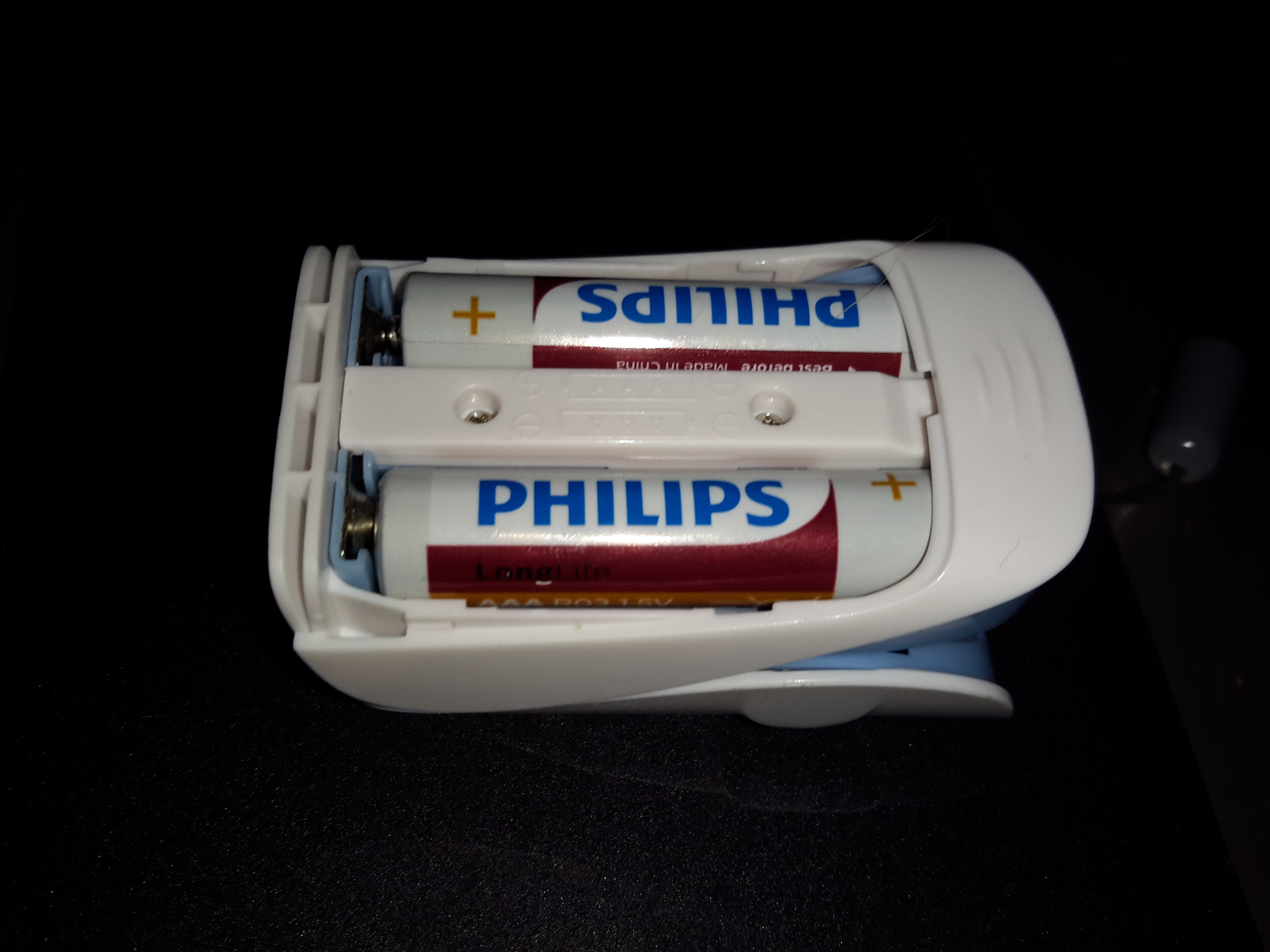
Battery Compartment
Power is supplied by a pair of AAA cells in the other shell.
Dual LED
The sensor LEDs are tucked in between the cells, this dual-diode package has a 660nm red LED & a 940nm IR LED.
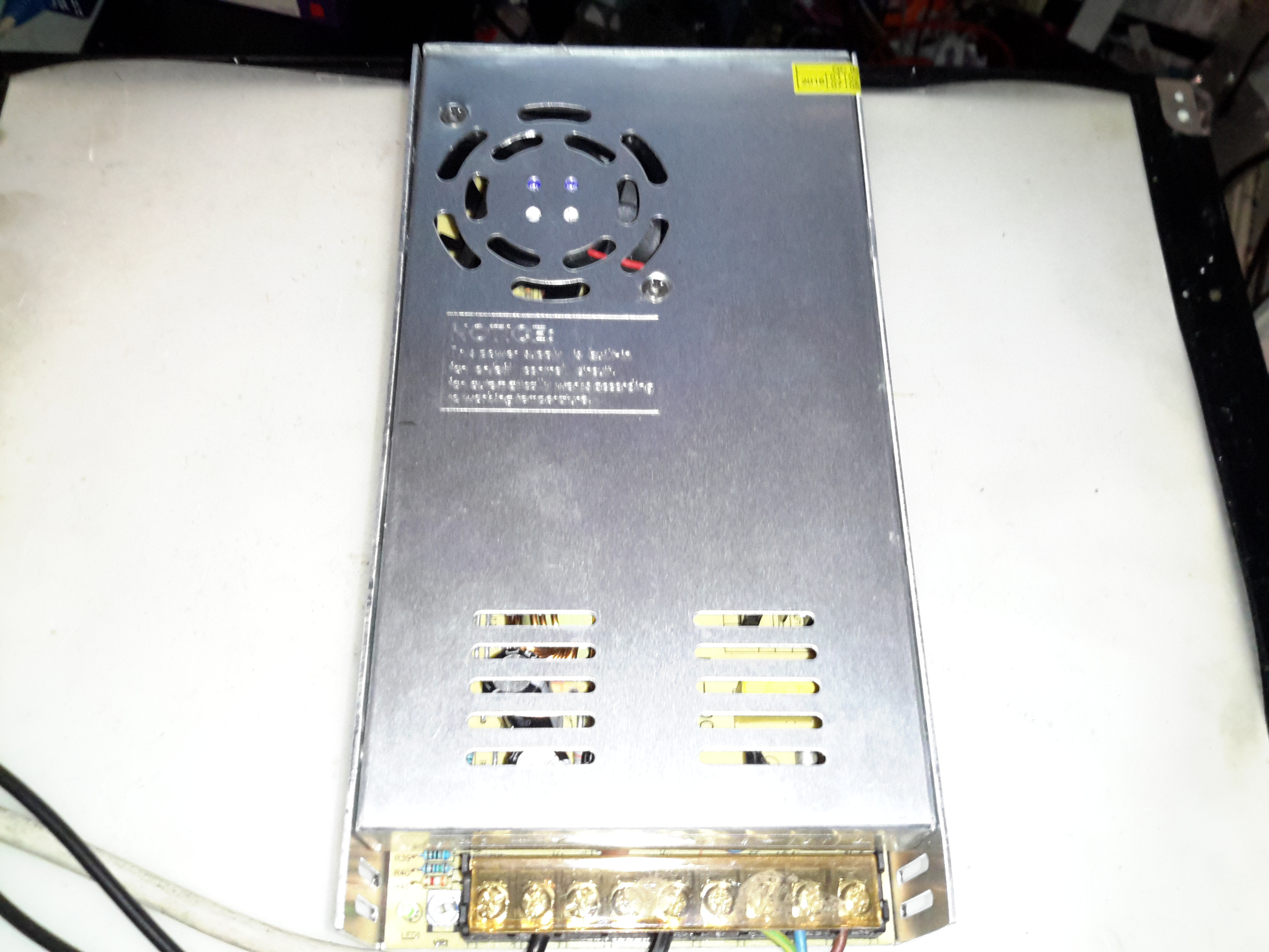
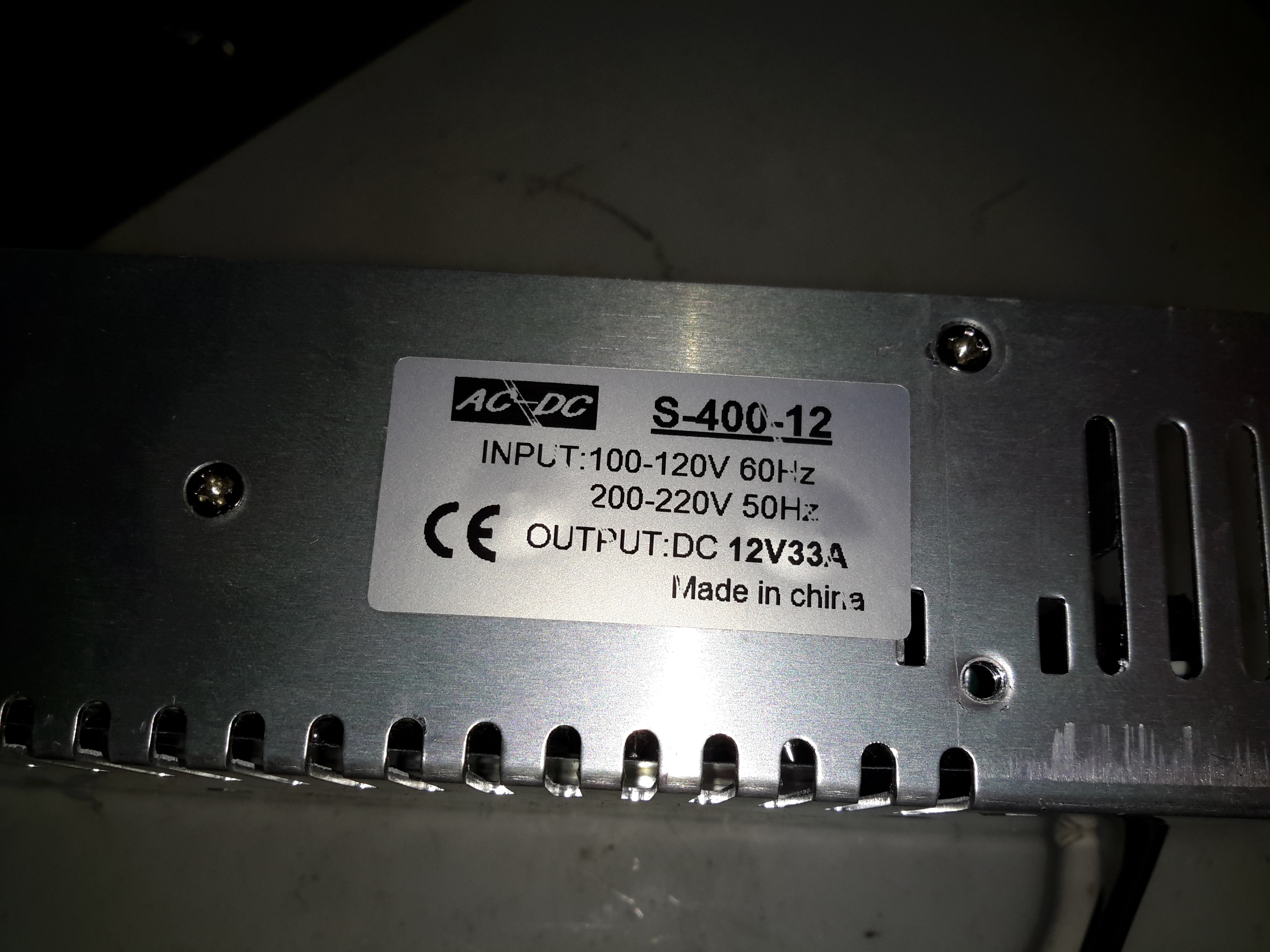
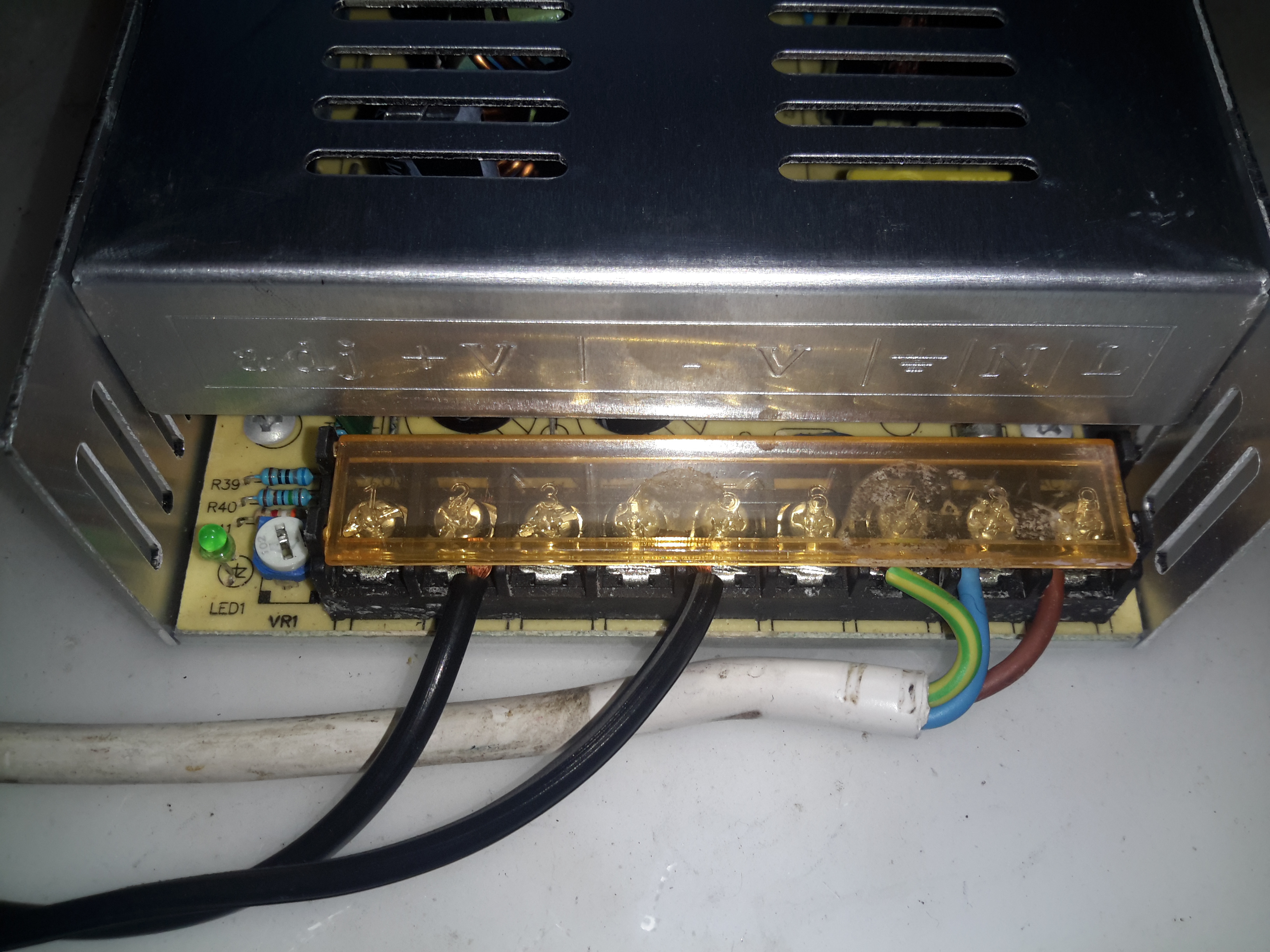
Here’s a cheap PSU from the treasure trove of junk that is eBay, rated at a rather beefy 400W of output at 12v – 33A! These industrial-type PSUs from name brands like TDK-Lambda or Puls are usually rather expensive, so I was interested to find out how much of a punishment these cheap Chinese versions will take before grenading. In my case this PSU is to be pushed into float charging a large lead acid battery bank, which when in a discharged state will try to pull as many amps from the charger as can be provided.
Rating Label
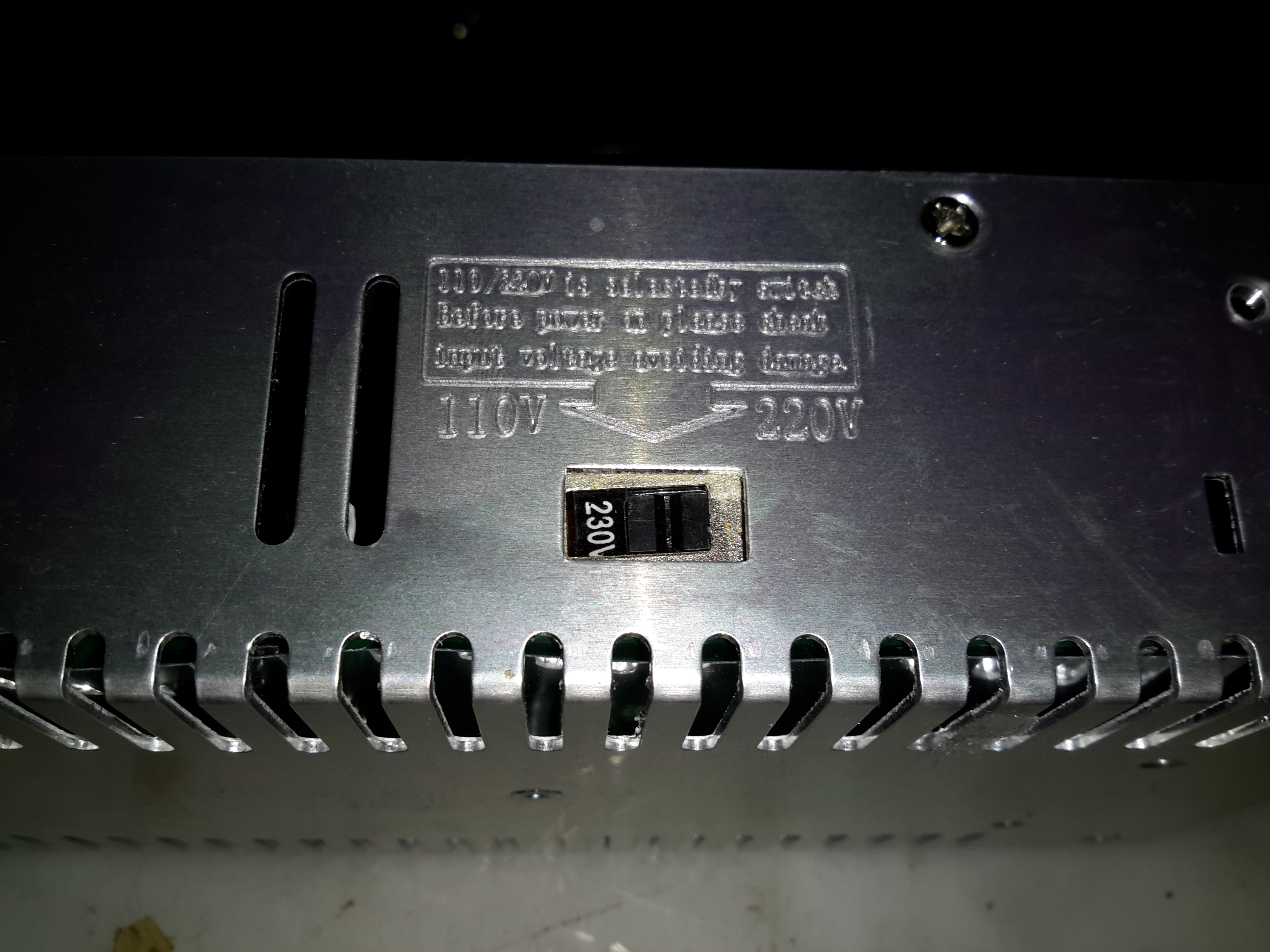
These PSUs are universal input, voltage adjustable by a switch on the other side of the PSU, below. The output voltage is also trimmable from the factory, an important thing for battery charging, as the output voltage needs to be sustained at 13.8v rather than the flat 12v from the factory.
Input Voltage SelectorMain Terminal Block
Mains connections & the low voltage outputs are on beefy screw terminals. The output voltage adjustment potentiometer & output indicator LED are on the left side.
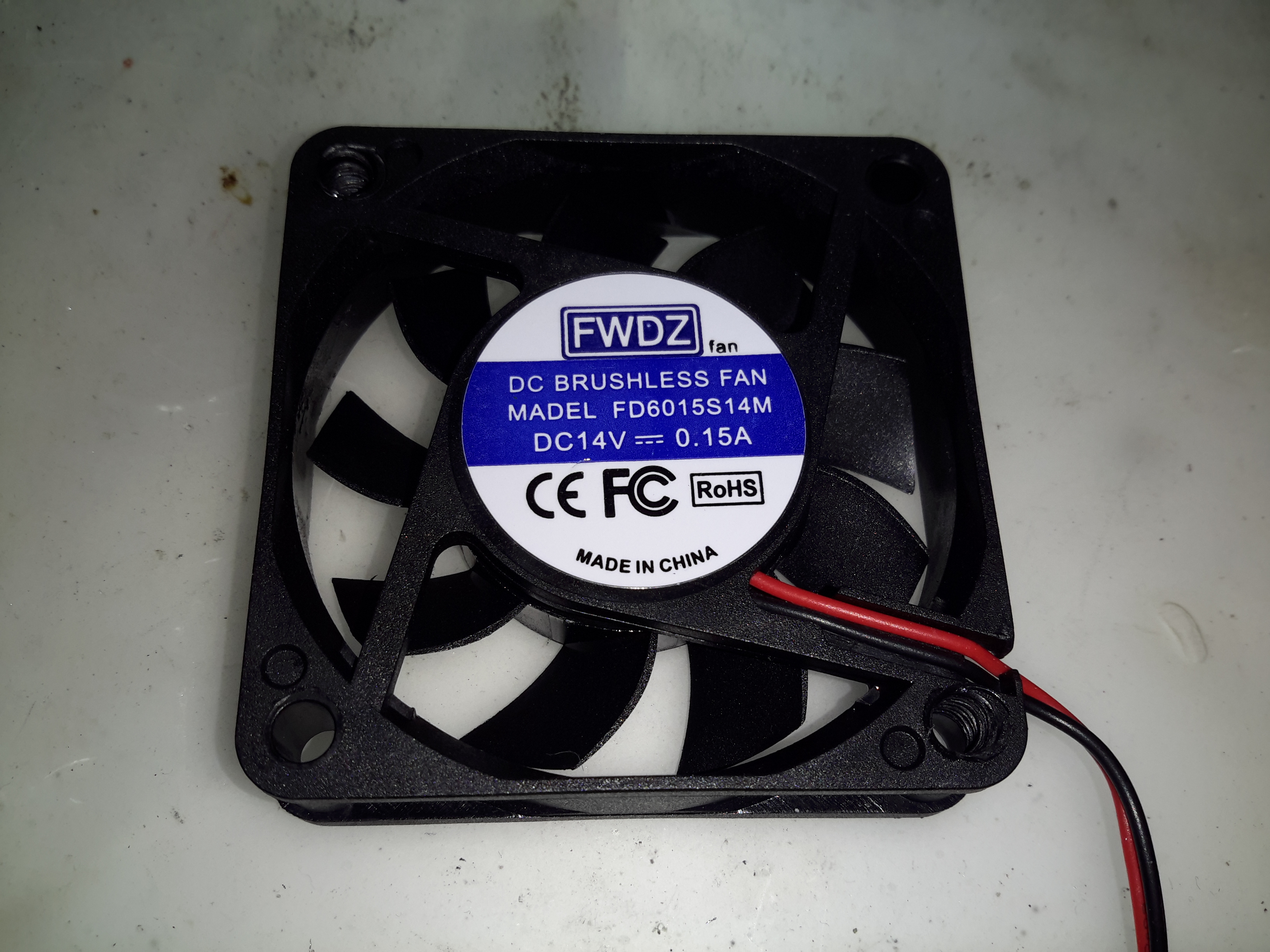
Cooling Fan
The cooling fan for the unit, which pulls air through the casing instead of blowing into the casing is a cheap sleeve bearing 60mm fan. No surprises here. I’ll probably replace this with a high-quality ball-bearing fan, to save the PSU from inevitable fan failure & overheating.
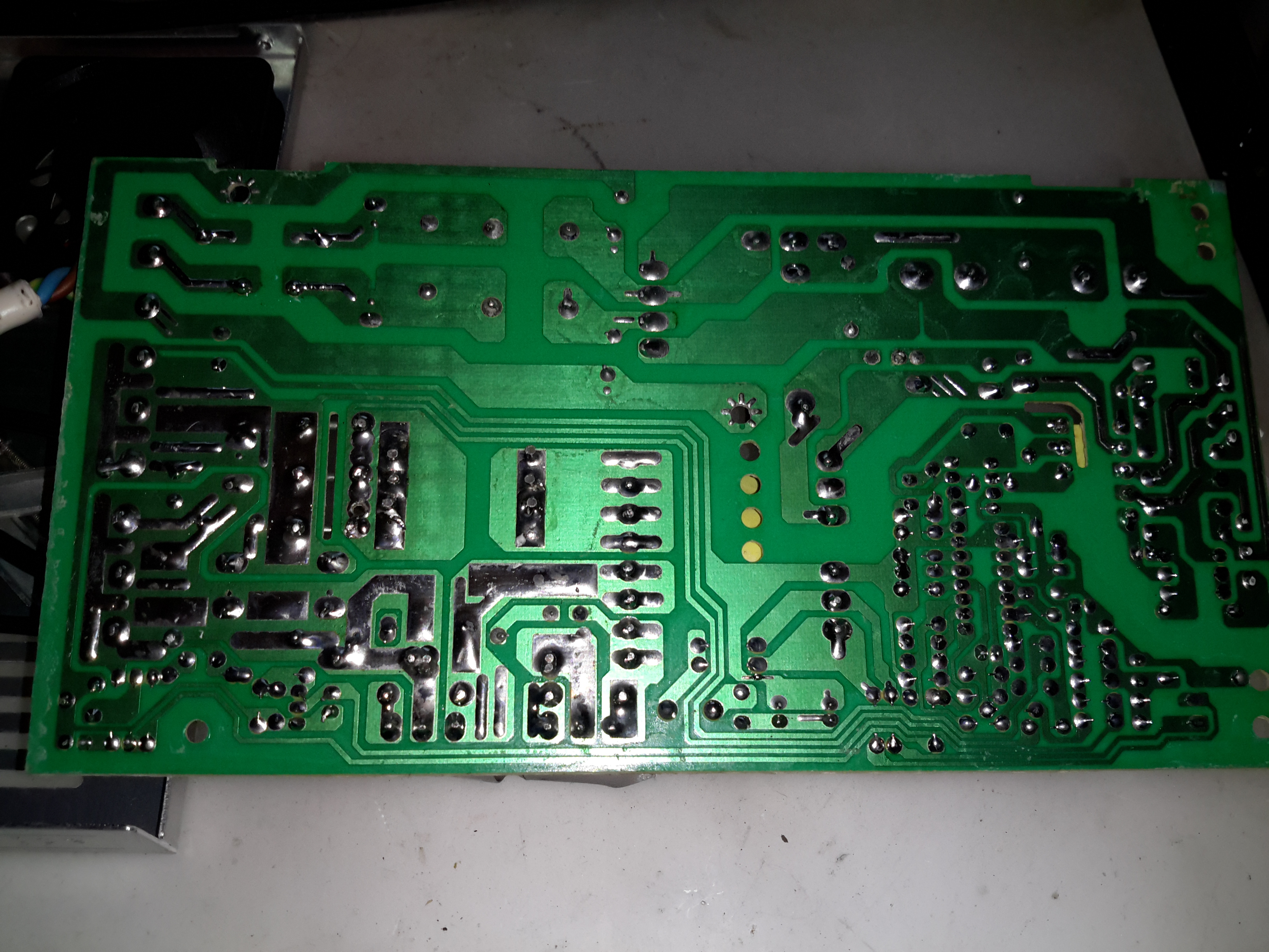
PCB Bottom
The PCB tracks are generously laid out on the high current output side, but there are some primary/secondary clearance issues in a couple of places. Lindsay Wilson over at Imajeenyus.com did a pretty thorough work-up on the fineries of these PSUs, so I’ll leave most of the in-depth stuff via a linky. There’s also a modification of this PSU for a wider voltage range, which I haven’t done in this case as the existing adjustment is plenty wide enough for battery charging duty.
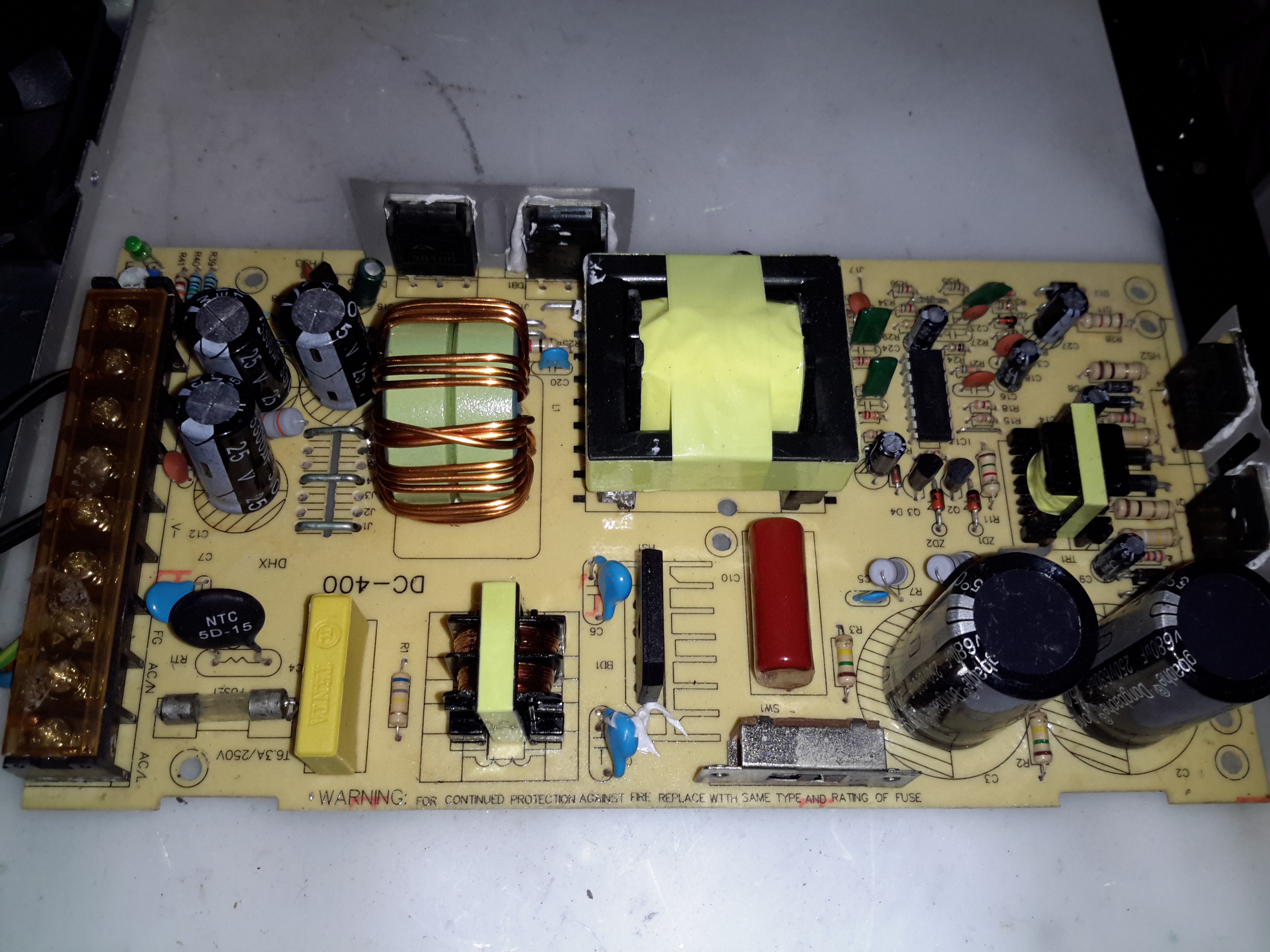
Bare PCB
The PCB is laid out in the usual fashion for these PSUs, with the power path taking a U-route across the board. Mains input is lower left, with some filtering. Main diode bridge in the centre, with the voltage selection switch & then the main filter caps. Power is then switched into the transformer by the pair of large transistors on the right before being rectified & smoothed on the top left.
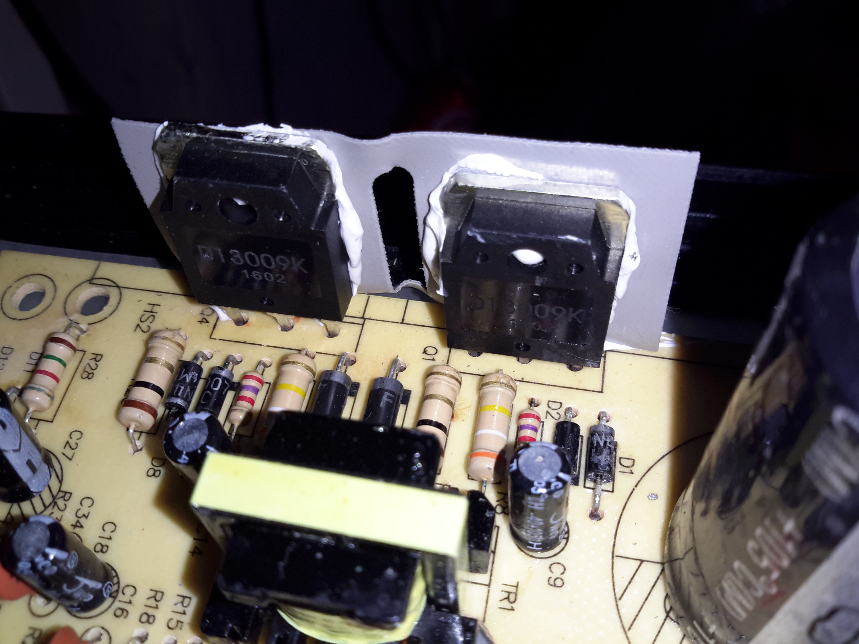
Main Switching Transistors
The pair of main switching devices are mounted to the casing with thermal compound & an insulating pad. To bridge the gap there’s a chunk of aluminium which also provides some extra heatsinking.
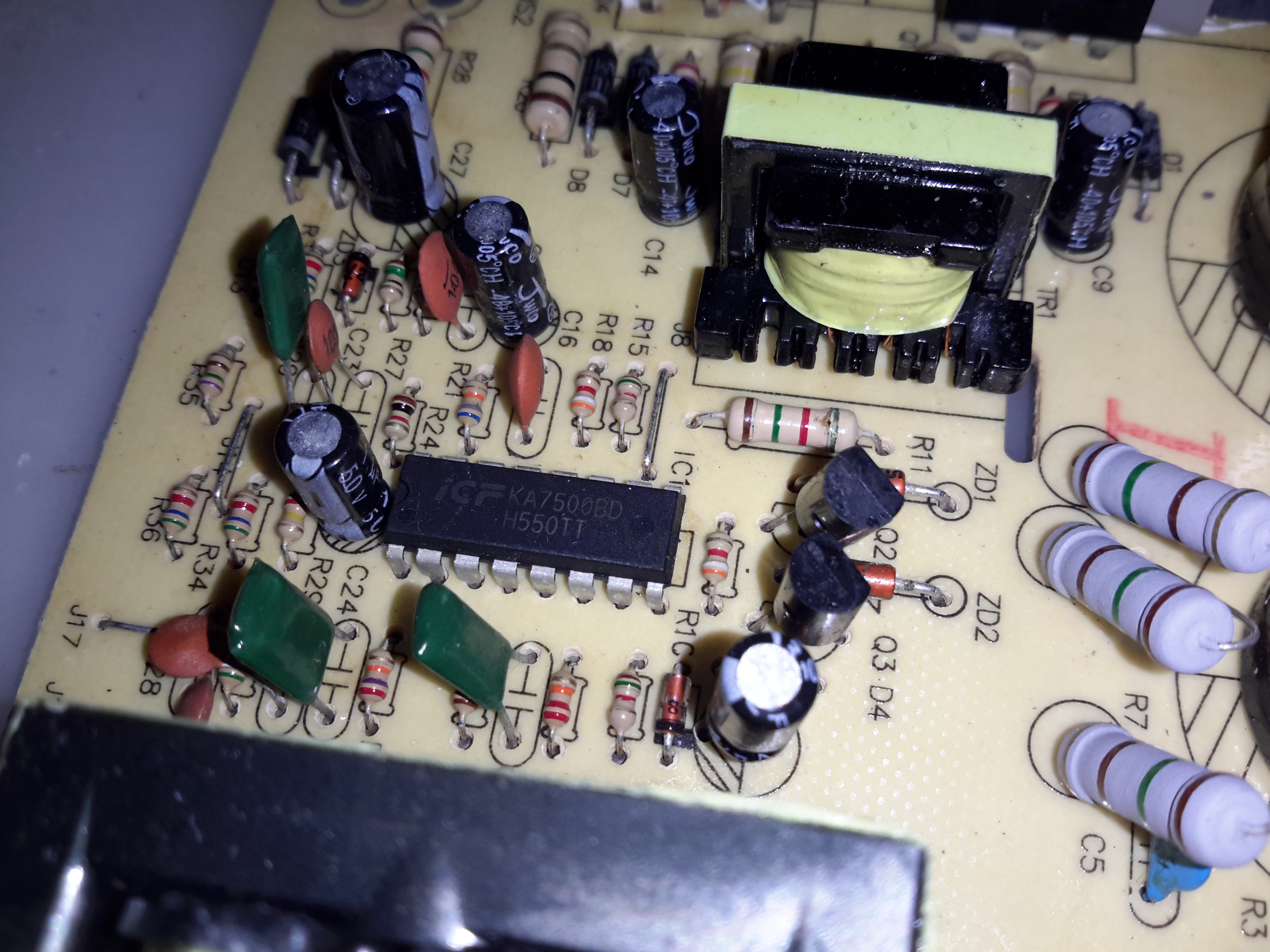
SMPS Drive IC & Base Drive Transformer
The PSU is controlled by a jelly-bean TL494 PWM controller IC. No active PFC in this cheap supply so the power factor is going to be very poor indeed.
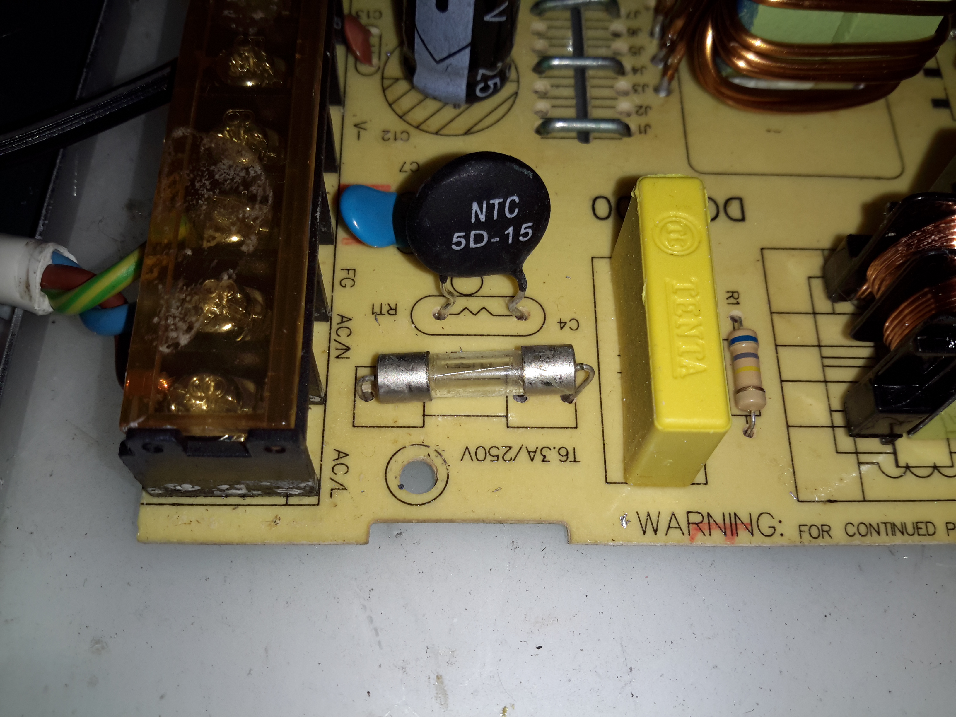
Input Protection
Input protection & filtering is rather simple with the usual fuse, MOV filter capacitor & common mode choke.
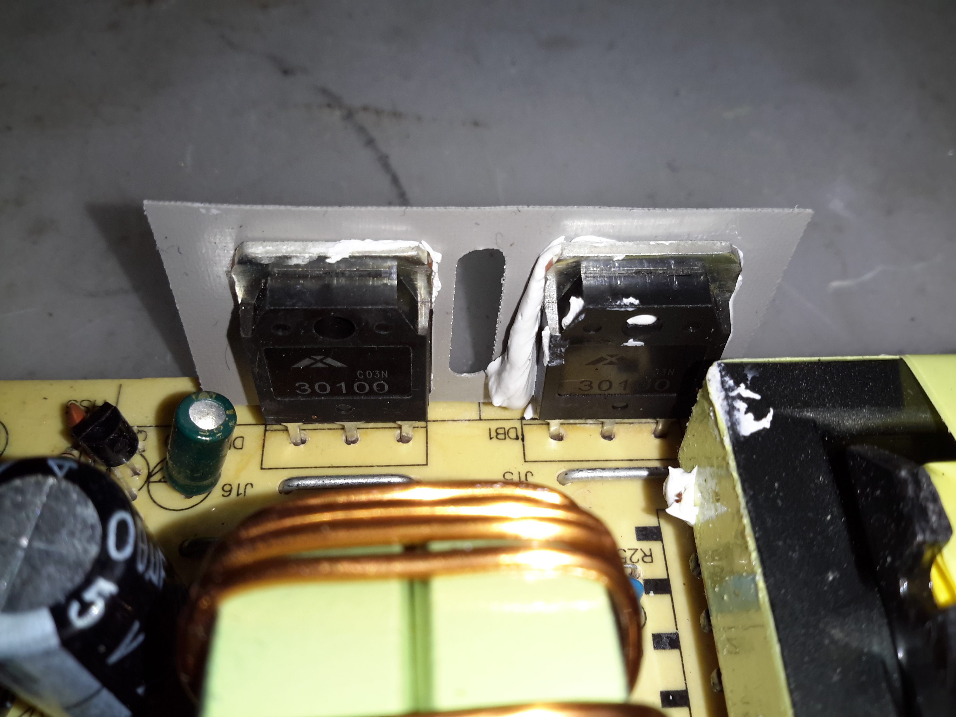
Main Output Rectifiers
Beefy 30A dual diodes on the DC output side, mounted in the same fashion as the main switching transistors.
Output Current Shunt
Current measurement is done by these large wire links in the current path, selectable for different models with different output ratings.
Hot Glue Support
The output capacitors were just floating around in the breeze, with one of them already having broken the solder joints in shipping! After reflowing the pads on all the capacitors some hot glue as flowed around them to stop any further movement.
This supply has now been in service for a couple of weeks at a constant 50% load, with the occasional hammering to recharge the battery bank after a power failure. at 13A the supply barely even gets warm, while at a load high enough to make 40A rated cable get uncomfortably warm (I didn’t manage to get a current reading, as my instruments don’t currently go high enough), the PSU was hot in the power semiconductor areas, but seemed to cope at full load perfectly well.
Tip Jar
If you’ve found my content useful, please consider leaving a donation by clicking the Tip Jar below!
All collected funds go towards new content & the costs of keeping the server online.