Having been a user of ownCloud for a long while, I decided to jump ship to the fork NextCloud for a few reasons, but the main one is that I never managed to get ownCloud to update itself (with the built-in updater app in the Admin panel) without completely shitting the bed, and as a result having to start from scratch & reupload all my files.
Nextcloud on the other hand has managed a major upgrade without any such problems, and the developers seem to be much more active than the ownCloud devs at present.
The one issue at the moment is that there are no packages for the Linux desktop client – it has to be built from scratch. This isn’t too difficult though, but to make things even easier I’ve thrown together a little bash script to automate the process. It’s tested to work under the latest version of Linux Mint (18.1), and does use a couple of commands that sudo won’t allow, so has to be run as root. It’s not polished in any way, but does work fine!
After the build process has completed, the client itself can be run from the Terminal, or made to run at system boot via the Startup Applications Editor in Linux Mint.
#!/bin/bash

echo "This script will compile & install Nextcloud Desktop Sync Client"
echo "Please be patient, this will take a while"

if [[ $EUID -ne 0 ]]; then
   echo "Root commands are used by this script, please run as root user to avoid errors"
   exit 1
fi

echo ""
echo "Installing Build Tools..."
echo ""
apt-get install cmake git-core -y

echo ""
echo "Cloning GitHub Repo..."
echo ""
git clone https://github.com/nextcloud/client_theming.git
cd client_theming
git submodule update --init --recursive

echo ""
echo "Adding Xenial Source Repos to /etc/apt/sources.list..."
echo ""

echo "deb-src http://archive.ubuntu.com/ubuntu/ xenial universe" >> /etc/apt/sources.list
echo "deb-src http://archive.ubuntu.com/ubuntu/ xenial-updates universe" >> /etc/apt/sources.list

echo ""
echo "Updating Apt & installing build dependencies..."
echo ""

apt-get update
apt build-dep owncloud-client -y

echo ""
echo "Compiling NextCloud Client..."
echo ""

mkdir build-linux
cd build-linux
cmake -D OEM_THEME_DIR=`pwd`/../nextcloudtheme ../client
make
make install

echo ""
echo "Adding Custom Library Directory Config..."
echo ""

echo "/usr/local/lib/x86_64-linux-gnu" >> /etc/ld.so.conf.d/x86_64-linux-gnu.conf
ldconfig

echo ""
echo "Nextcloud Client has been built & installed!"
echo ""
exit 0
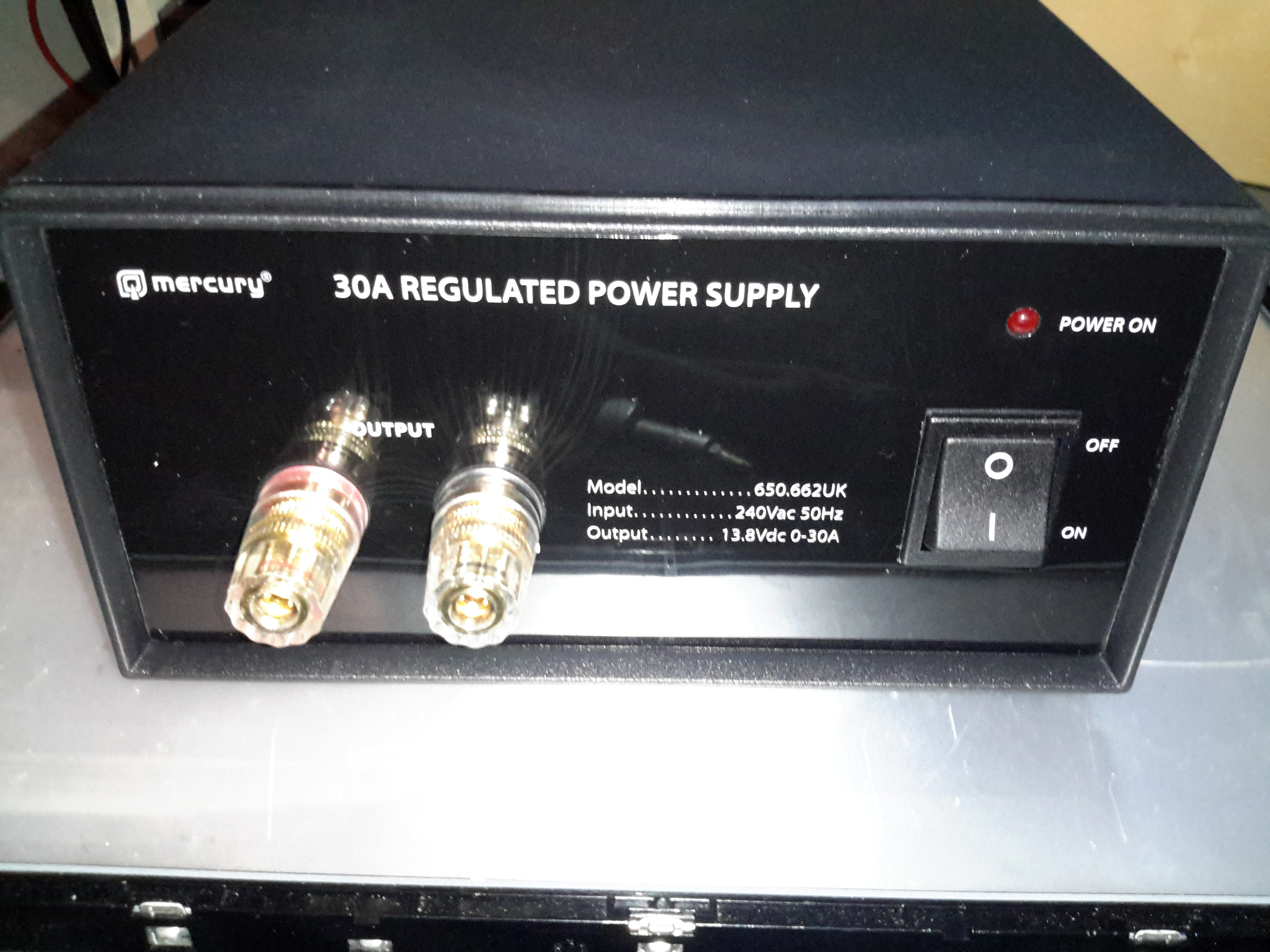
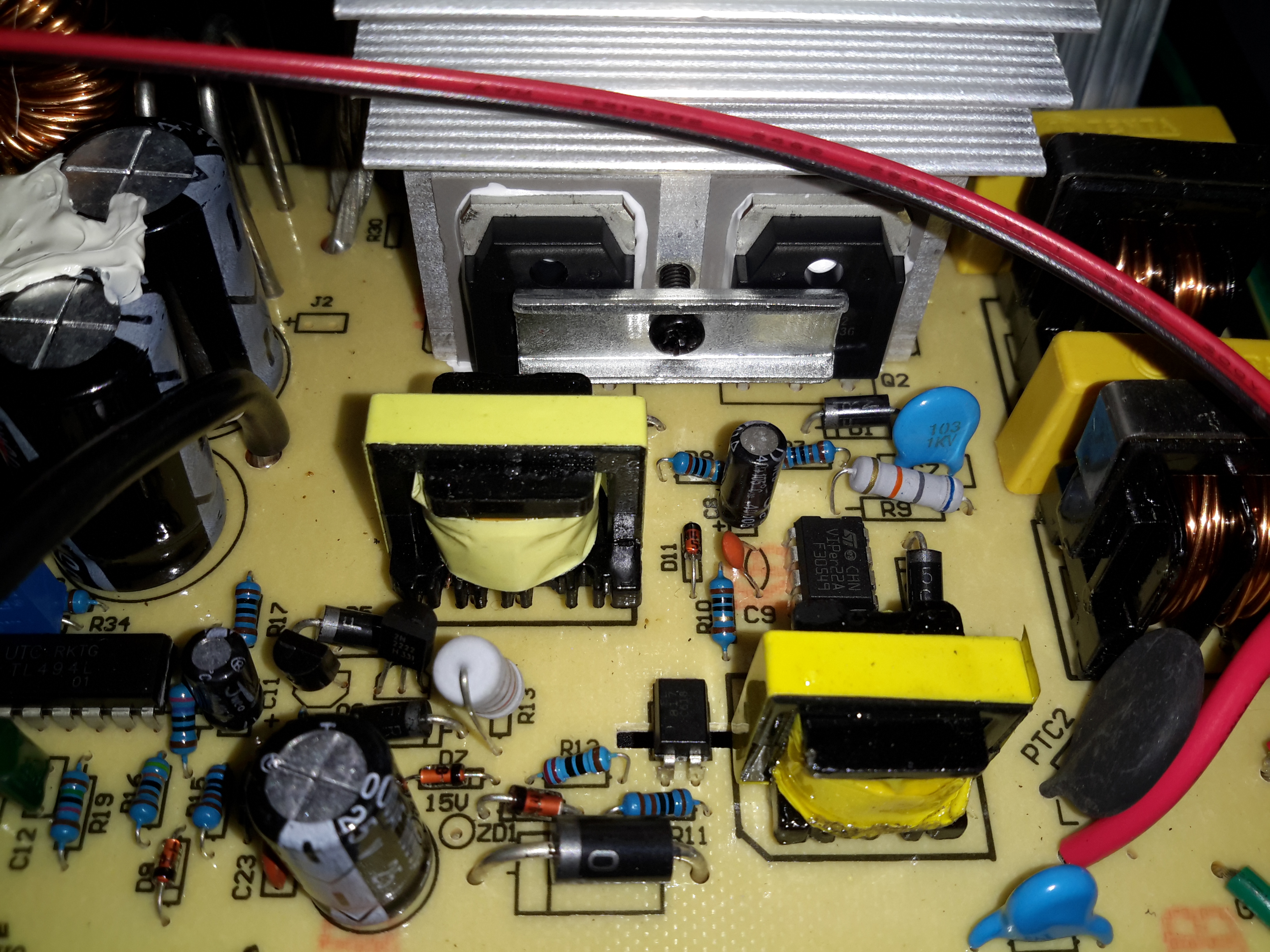
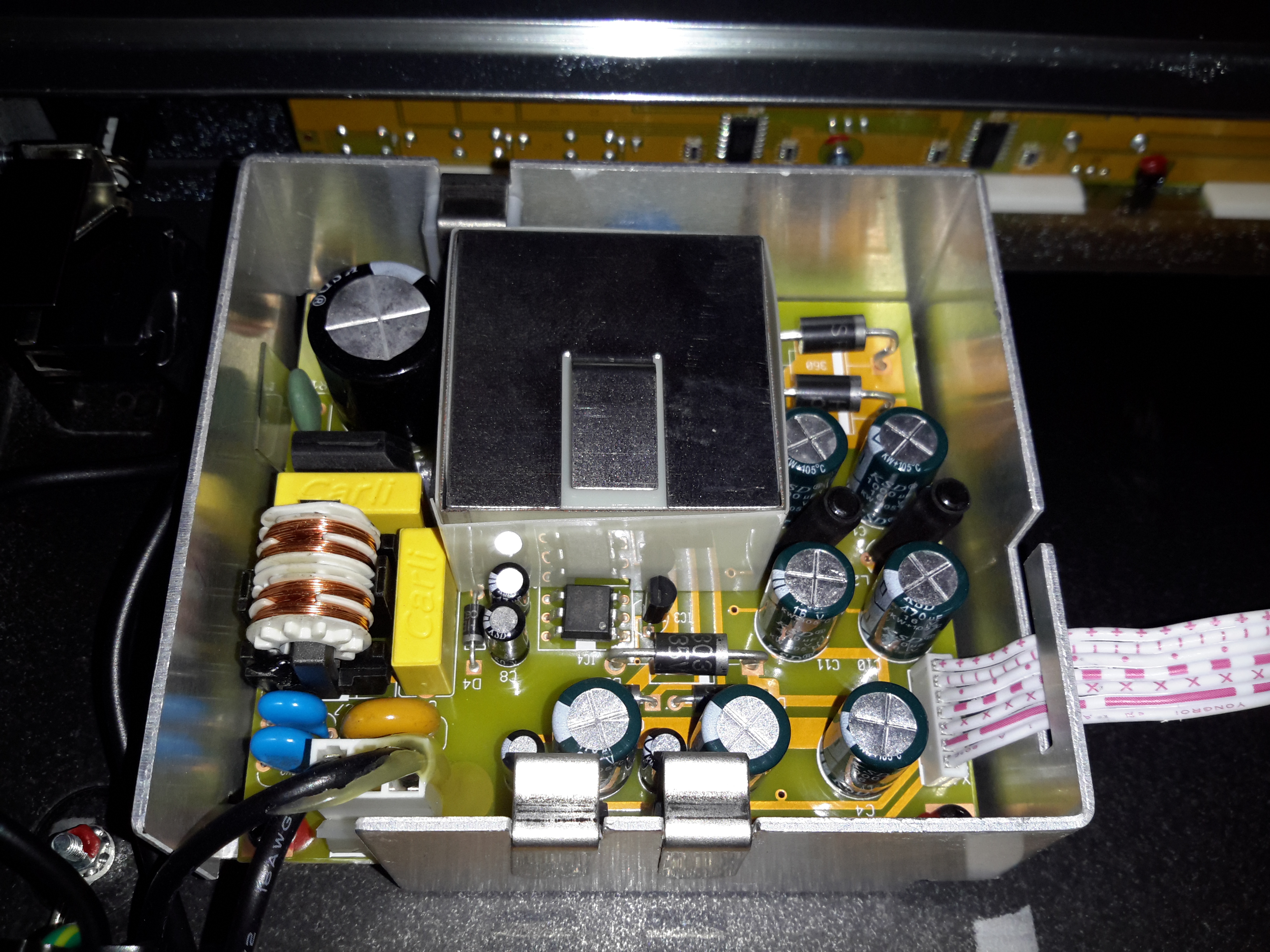
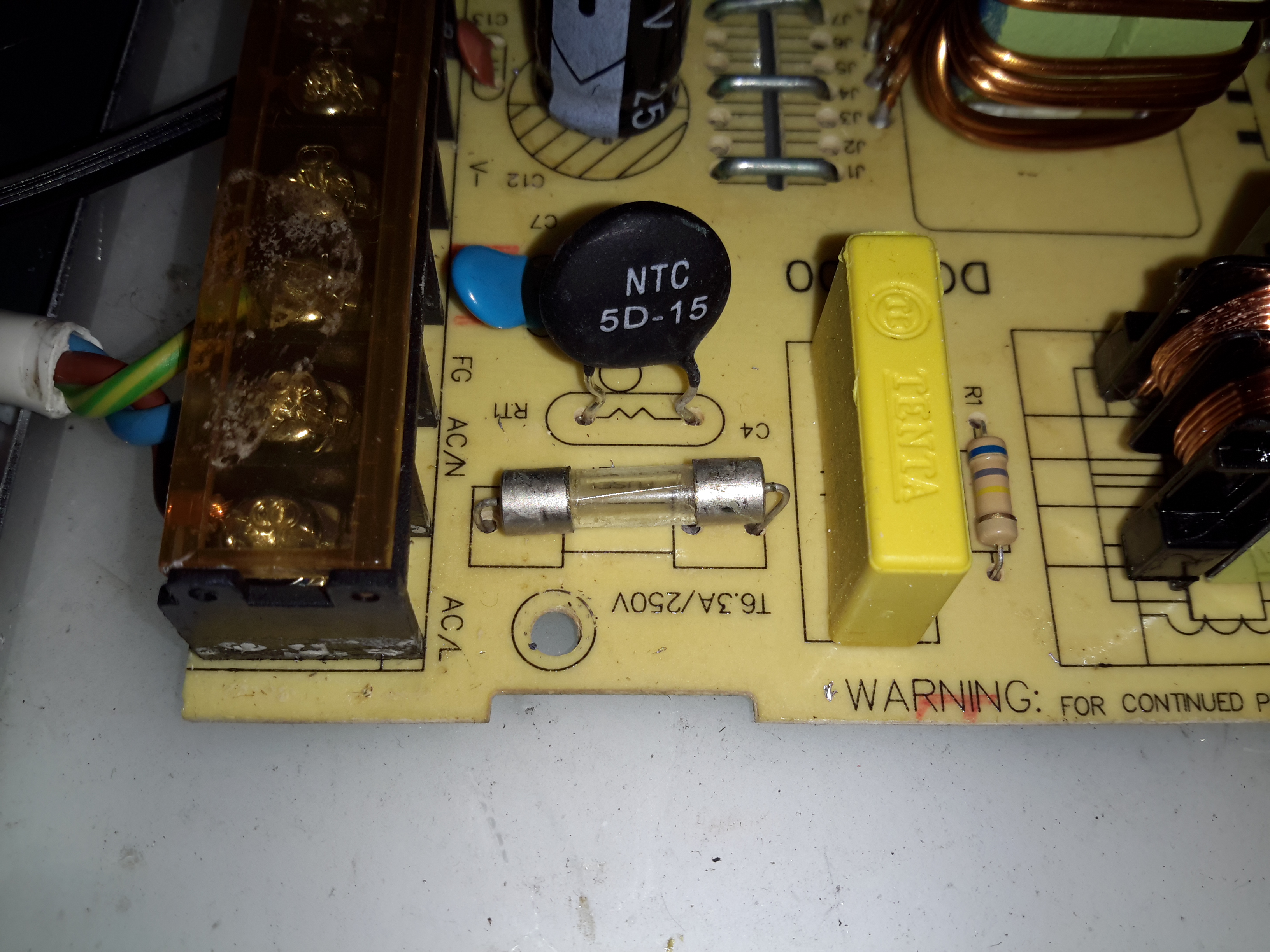
After having a couple of the cheap Chinese PSUs fail on me in a rather spectacular fashion, I decided to splash on a more expensive name-brand PSU, since constantly replacing PSUs at £15 a piece is going to get old pretty fast. This is the 30A model from Mercury, which seems to be pretty well built. It’s also significantly more expensive at £80. Power output is via the beefy binding posts on the front panel. There isn’t any metering on board, this is something I’ll probably change once I’ve ascertained it’s reliability. This is also a fixed voltage supply, at 13.8v.
Rear Panel
Not much on the rear panel, just the fuse & cooling fan. This isn’t temperature controlled, but it’s not loud. No IEC power socket here, the mains cable is hard wired.
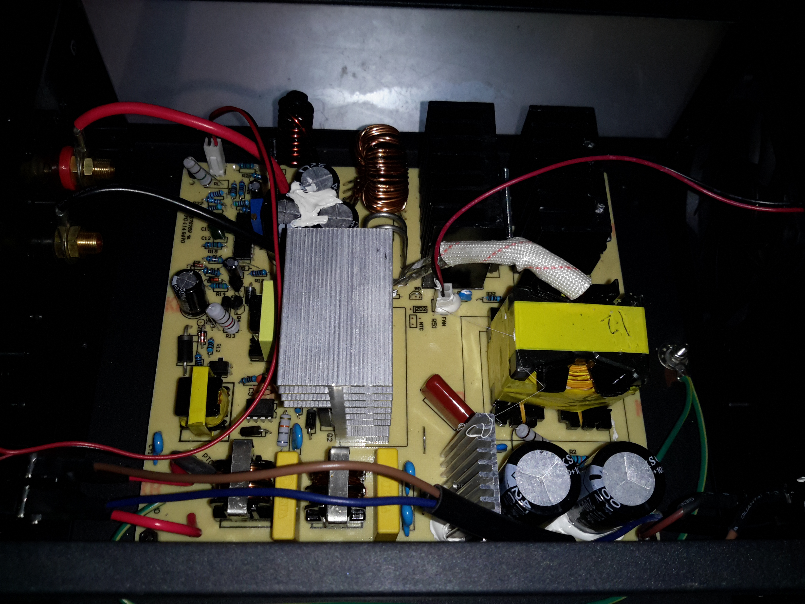
Main Board
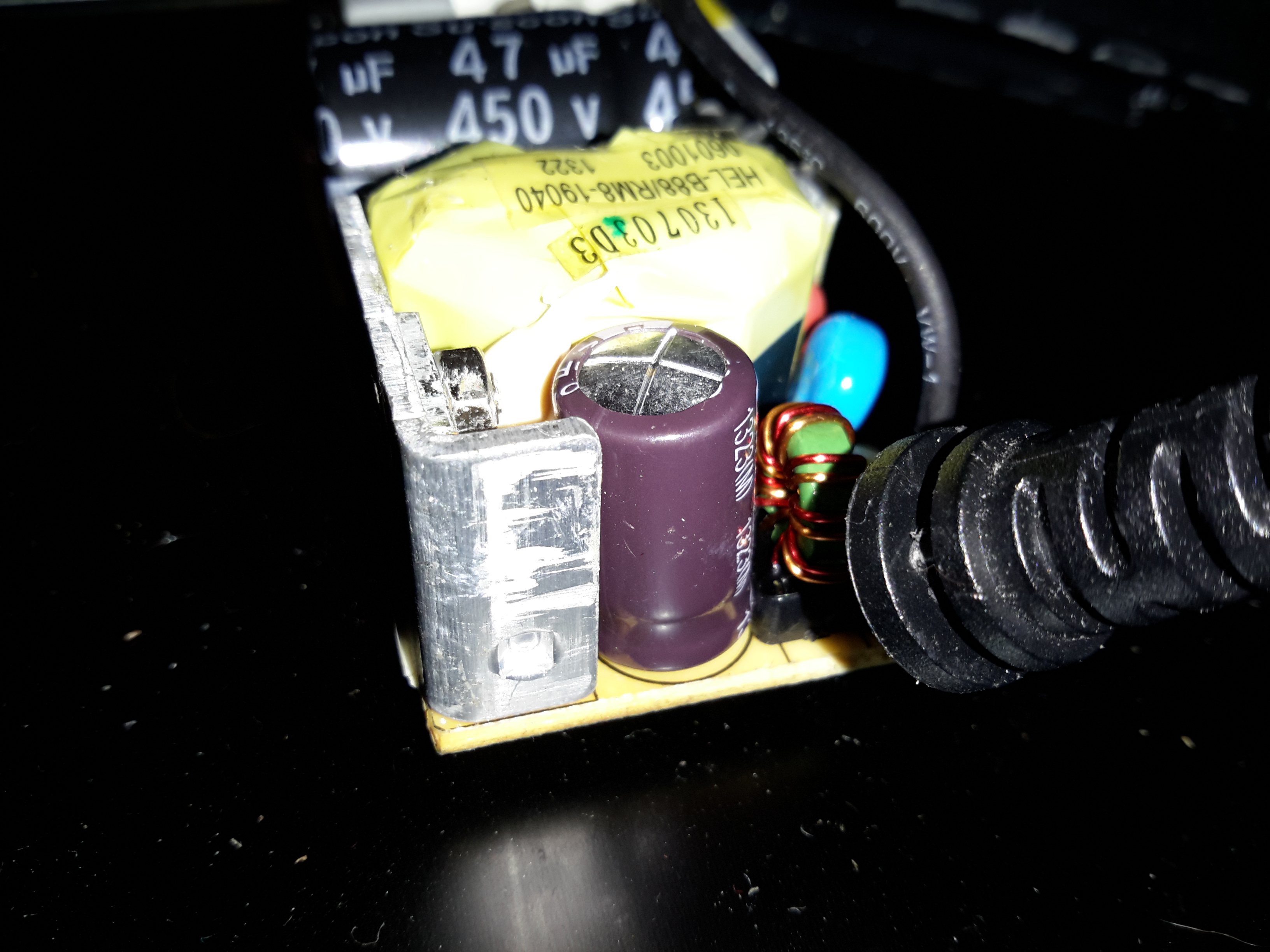
Removing some spanner-type security screws reveals the power supply board itself. Everything on here is enormous to handle the 30A output current at 13.8v. The main primary side switching transistors are on the large silver heatsink in the centre of the board, feeding the huge ferrite transformer on the right.
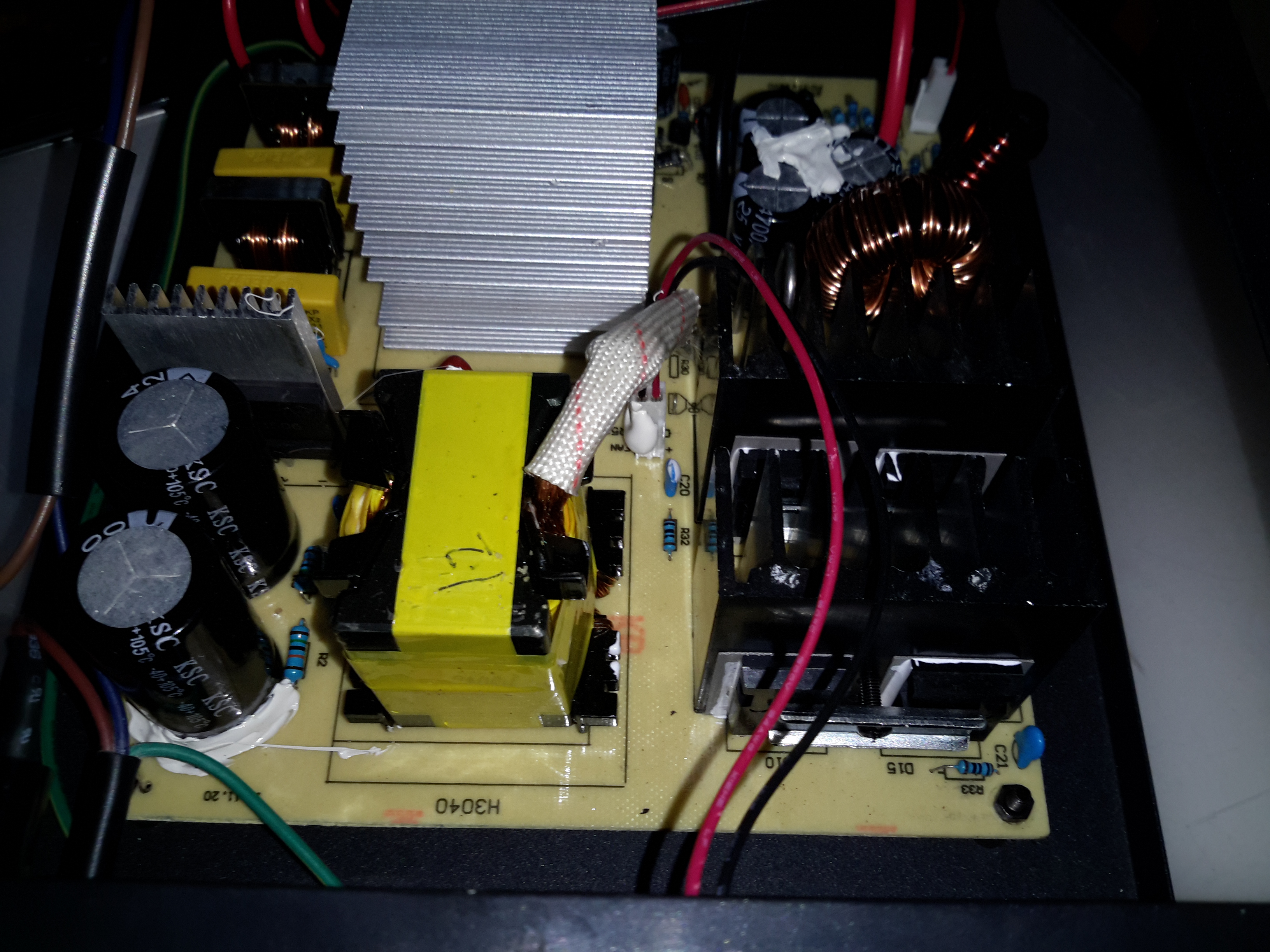
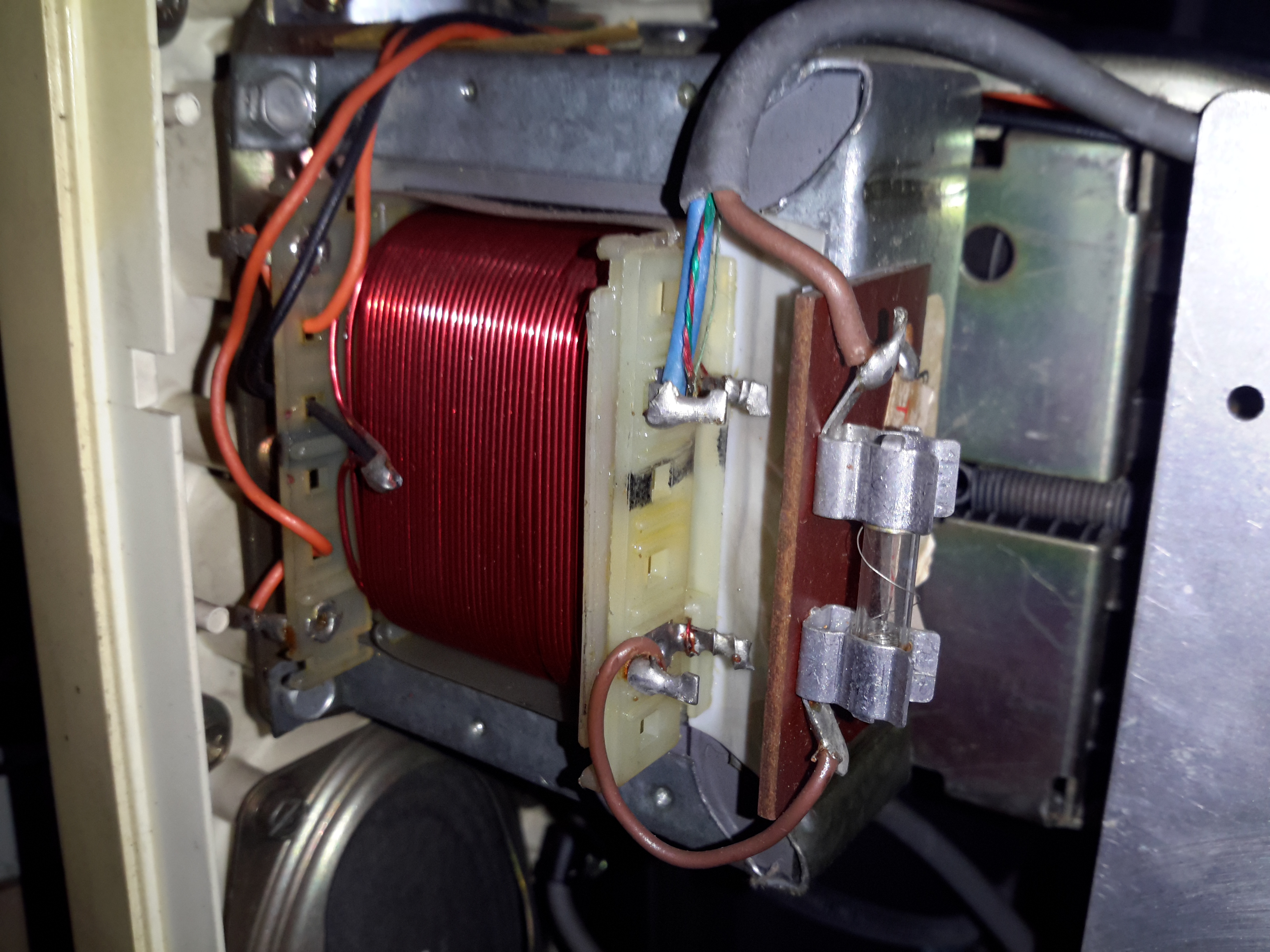
Transformer
The transformer’s low voltage output tap comes straight out instead of being on pins, due to the size of the winding cores. Four massive diodes are mounted on the black heatsinks for output rectification.
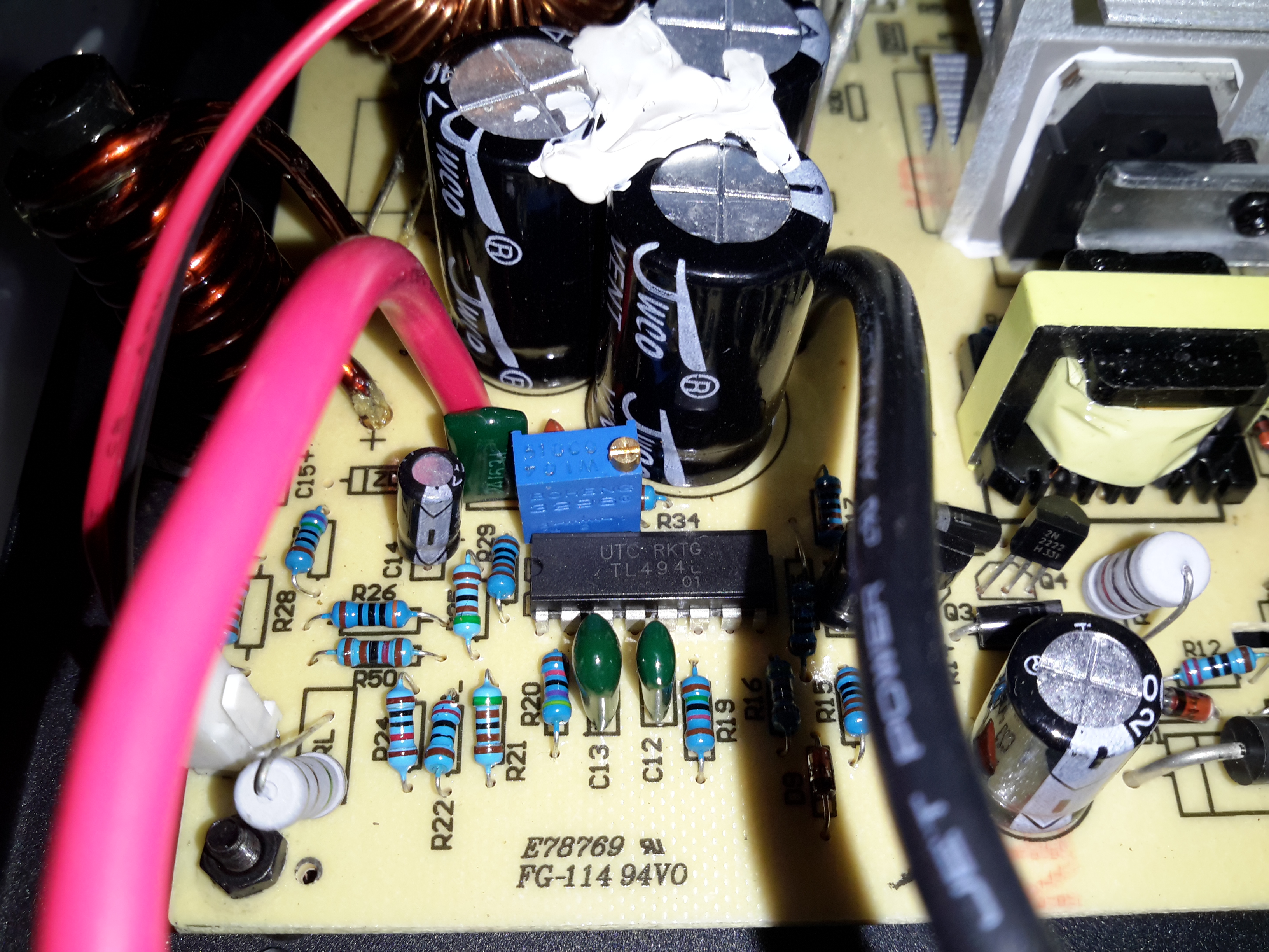
SMPS Controller
The supply is controlled via the jelly bean TL494 PWM controller IC. The multi-turn potentiometer doesn’t adjust the output voltage, more likely it adjusts the current limit.
Standby Supply
Power to initially start the supply is provided by a small SMPS circuit, with a VIPer22A Low Power Primary Switcher & small transformer on the lower right. The transformer upper left is the base drive transformer for the main high power supply.
In a word, no they aren’t any good. As usual, cheap doesn’t equal good, and in this case the cheapo clones are a total waste of money. Read on for the details!
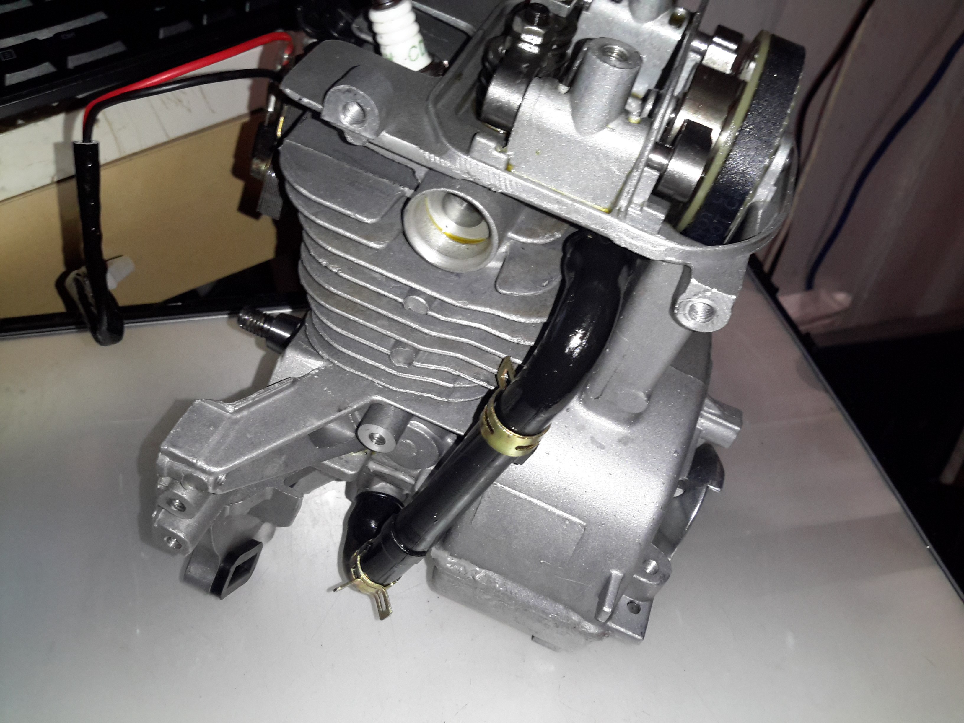
I’ve been looking into using a cheap Chinese clone Honda GX35 engine to drive an automotive alternator as a portable battery charging & power unit. These engines are available very cheaply on eBay, aimed at the mini-bike/go-kart market.
For those not in the know, the Honda GX25/35 4-strokes are strimmer-type engines that traditionally were always of 2-stroke construction. Honda worked out how to have a wet-sump engine without the need to keep the engine always in the “upright” position. They do not require mixing of oil into the fuel for lubrication as 2-strokes do, so should be much cleaner running.
So far I’ve had two of these cheap engines, as the first one died after only 4 hours run time, having entirely lost compression. At the time the engine was idling, no load, having been started from cold only a few minutes before. Having checked the valve clearances to make sure a valve wasn’t being held partially open, I deduced that the cause was broken piston rings. This engine was replaced by the seller, so I didn’t get a chance to pull it to bits to find out, but I decided to do a full teardown on the replacement to see where the cloners have cut corners.
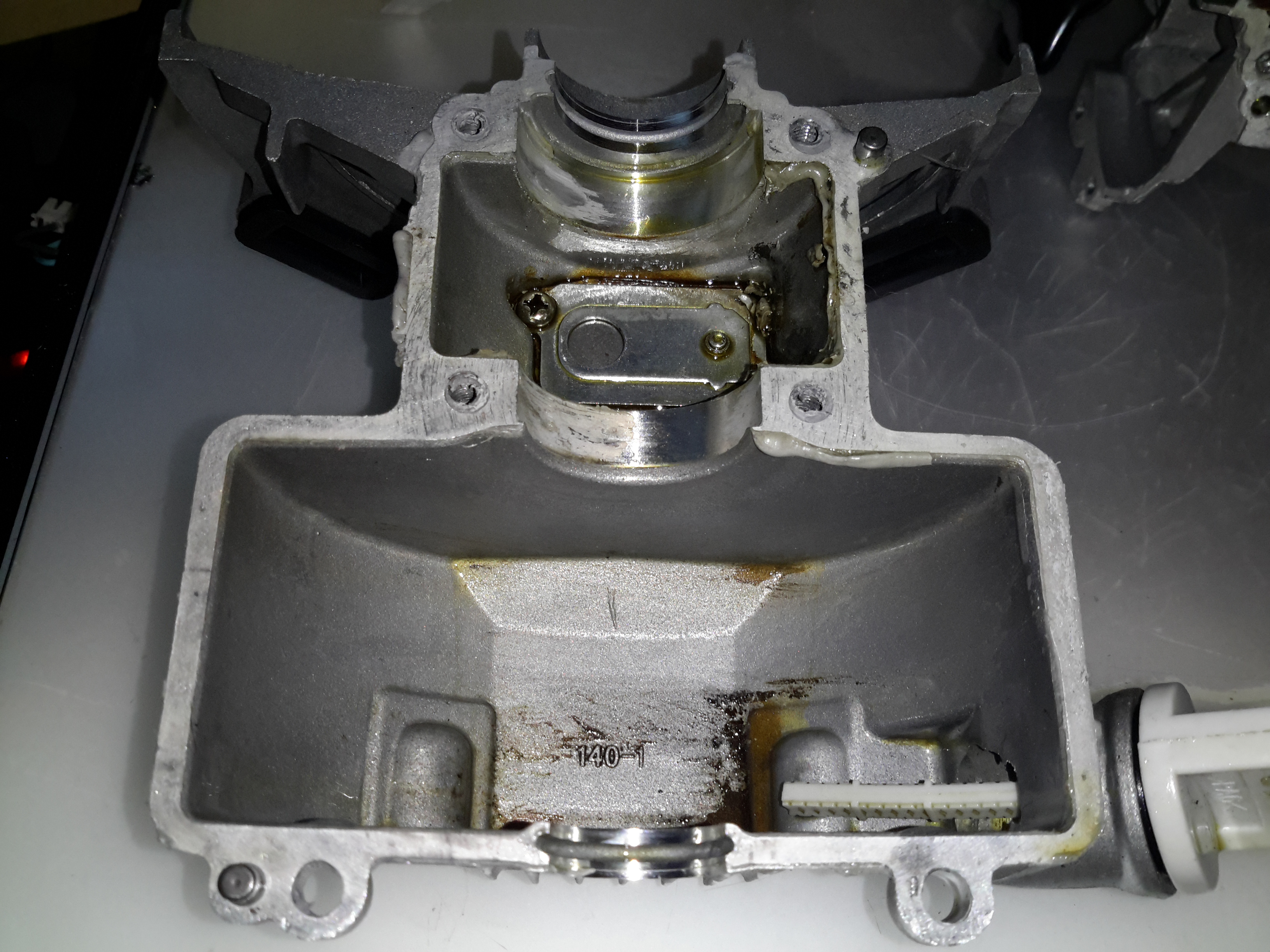
Oil Return Hose
I’ve already stripped off the ancillary components: exhaust, carburettor, fuel tank, cowlings, as these parts are standard to any strimmer engine. The large black hose here is the oil return feed back to the rocker cover from the crankcase. The oiling system in these engines is rather clever. The main engine block is made of light alloy, probably some permutation of Aluminium. There is much flashing left behind between the cylinder fins from the die-casting process, and not a single engine manufacturer’s logo anywhere. (From what I’ve read, the genuine Honda ones have their logo on the side of the crankcase).
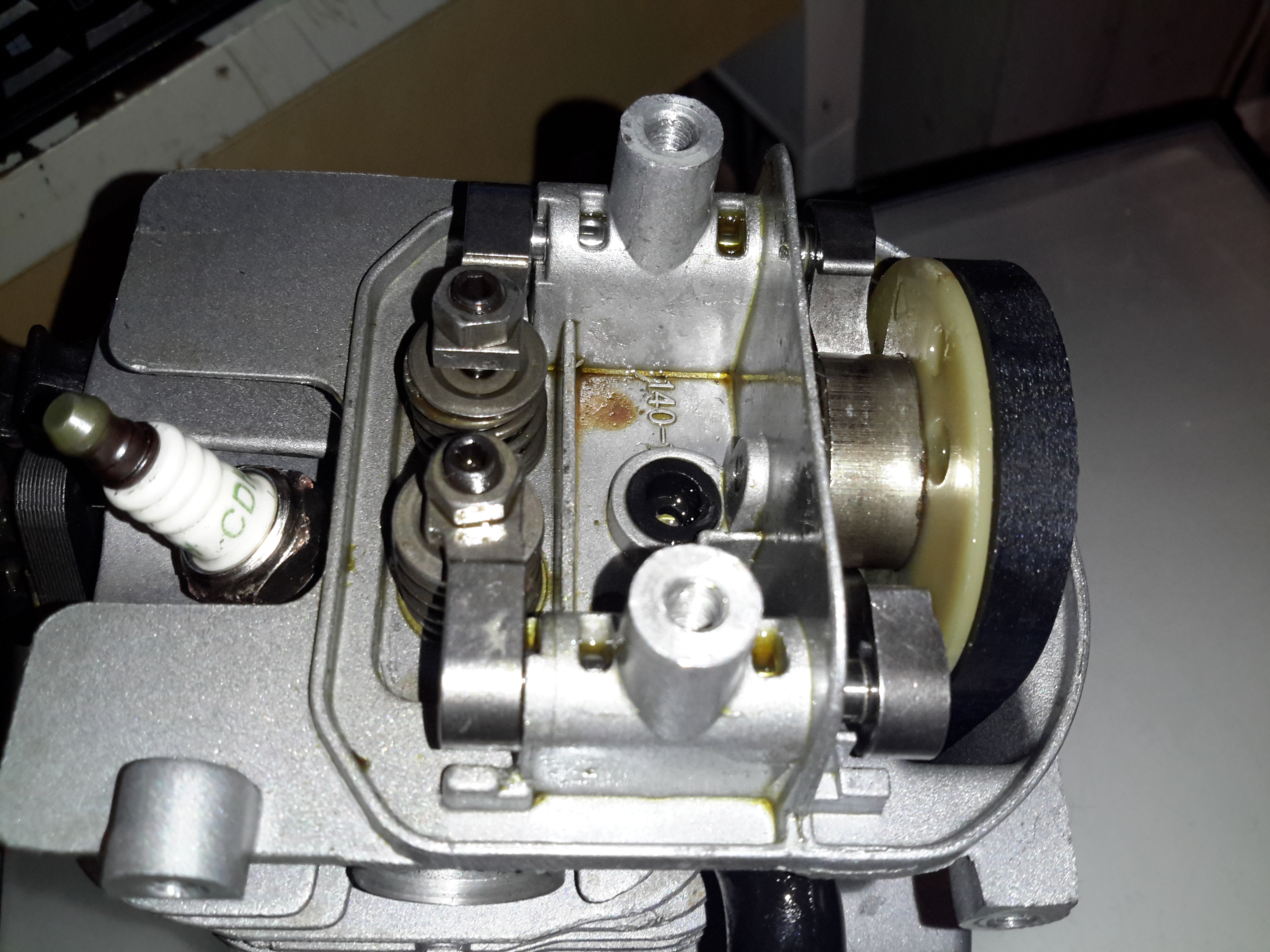
Rocker Box
Here’s the top of the engine with valves, rockers & camshaft. All the valve gear up here, minus the valves themselves & springs, are manufactured from sintered steel, there are no proper “bearings”, the steel shafts just run in the aluminium castings. The cam gear is of plastic, with the sintered steel cam pressed into place. The cam also has the bearing surface for the pin that the whole assembly rotates on. The timing belt runs in the oil & is supposed to last the life of the engine, and while I’d believe that in the original Honda, I certainly wouldn’t in this engine. The black grommet is the opening of the oil return gallery.
Cam
Here’s the cam on the back of the plastic pulley. A single cam is used for both intake & exhaust valves for space & simplicity.
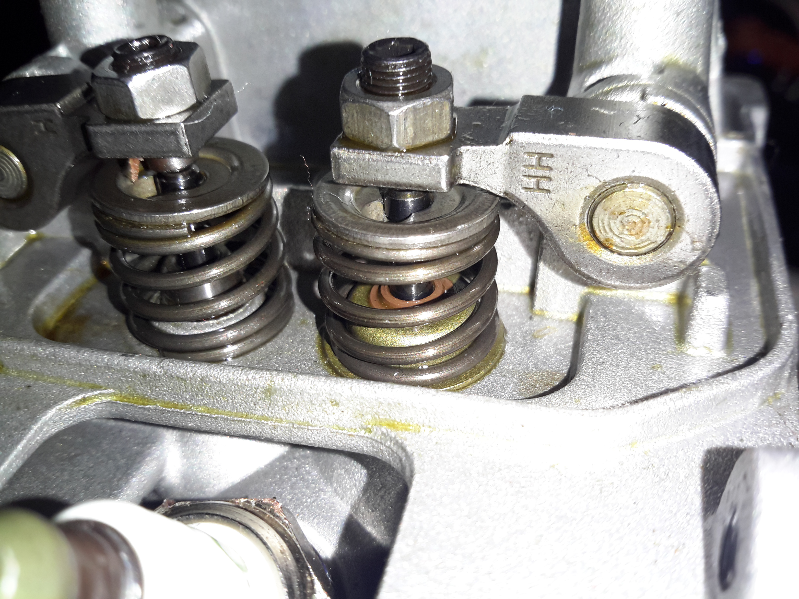
Intake Valve Stem Seal
Just visible under the intake valve spring is a simple stem seal, to hopefully prevent oil being sucked down the valve guide into the cylinder by intake vacuum. Running these cheap engines proves this seal to be ineffective, as they blow about as much blue oil smoke as a 2-stroke when they’re started cold. 😉
Starter Side
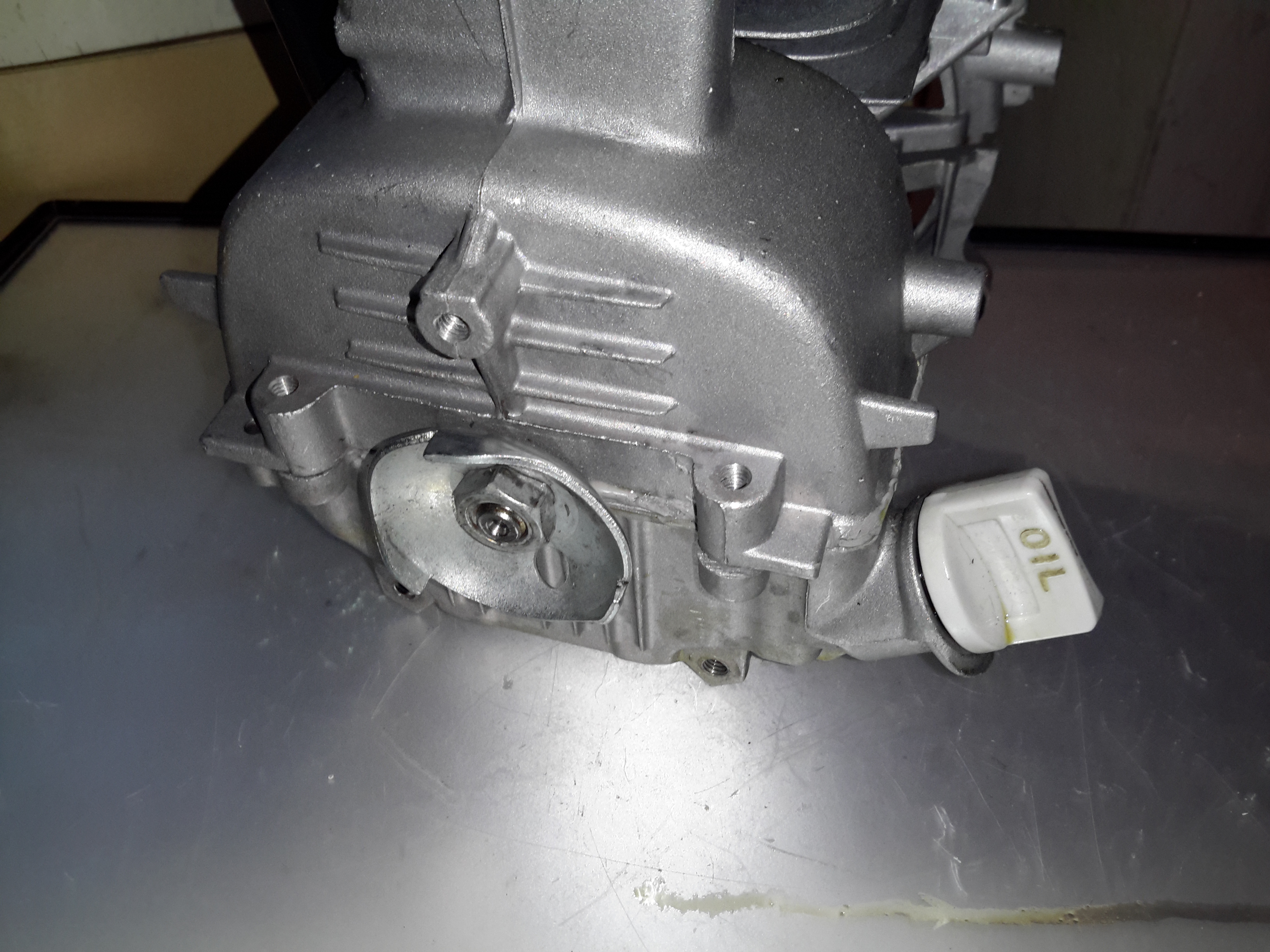
The starter side is where the oil sump is located on these engines, along with the dipstick.
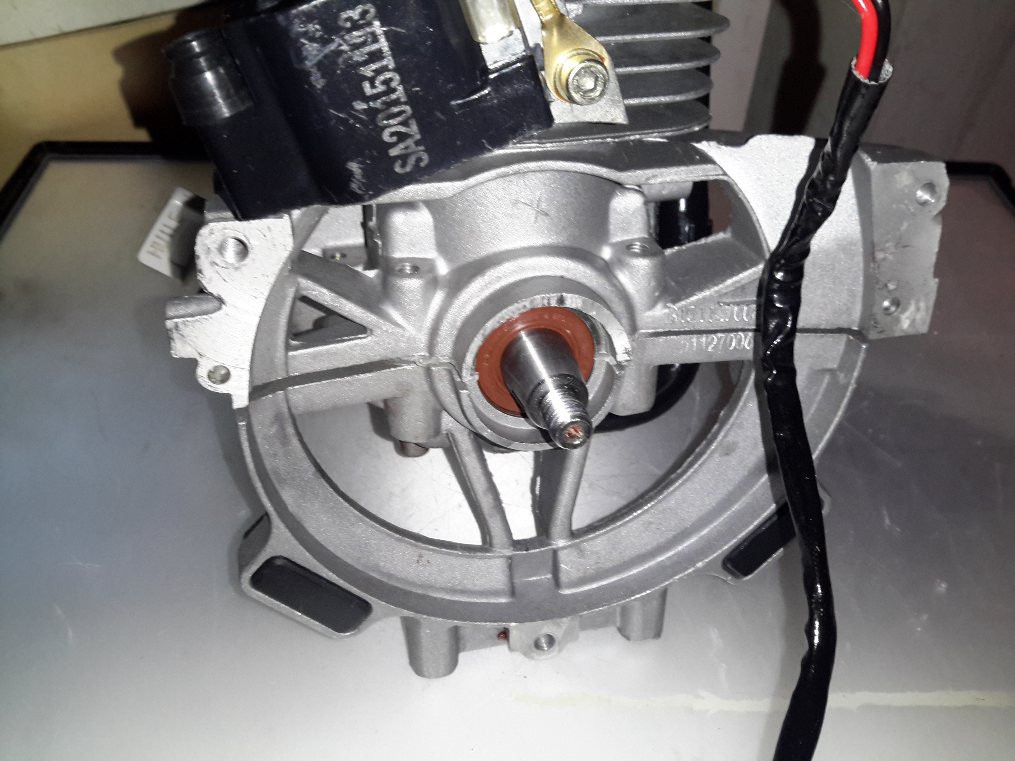
Flywheel Side
The flywheel end of the engine is the usual fare for small engines. Ignition is provided by a magneto, with a magnet in the flywheel. This is no different from the 2-stroke versions. As these ignitions fire on every revolution of the crankshaft, the spark plug fires both on compression, igniting the fuel for normal operation, and again into the exhaust stroke, where the spark is wasted.
One thing I have noticed about these engines is an almost total lack of cooling air coming through the cowling over the cylinder cooling fins. Plenty was flowing over the exhaust silencer side, I believe bad housing design would be what causes this problem. A lack of cooling certainly wouldn’t help engine longevity!
Engine “Sump”
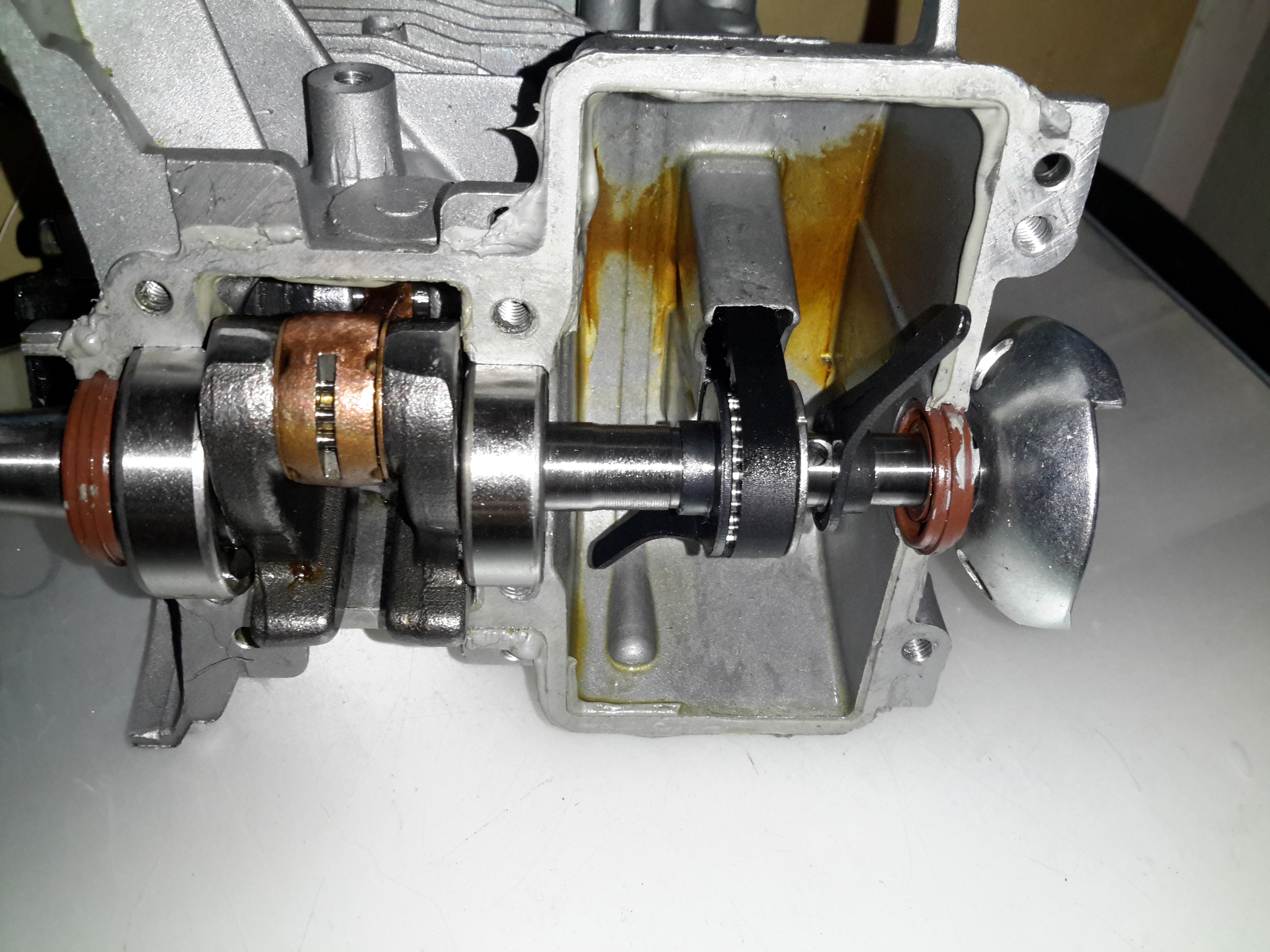
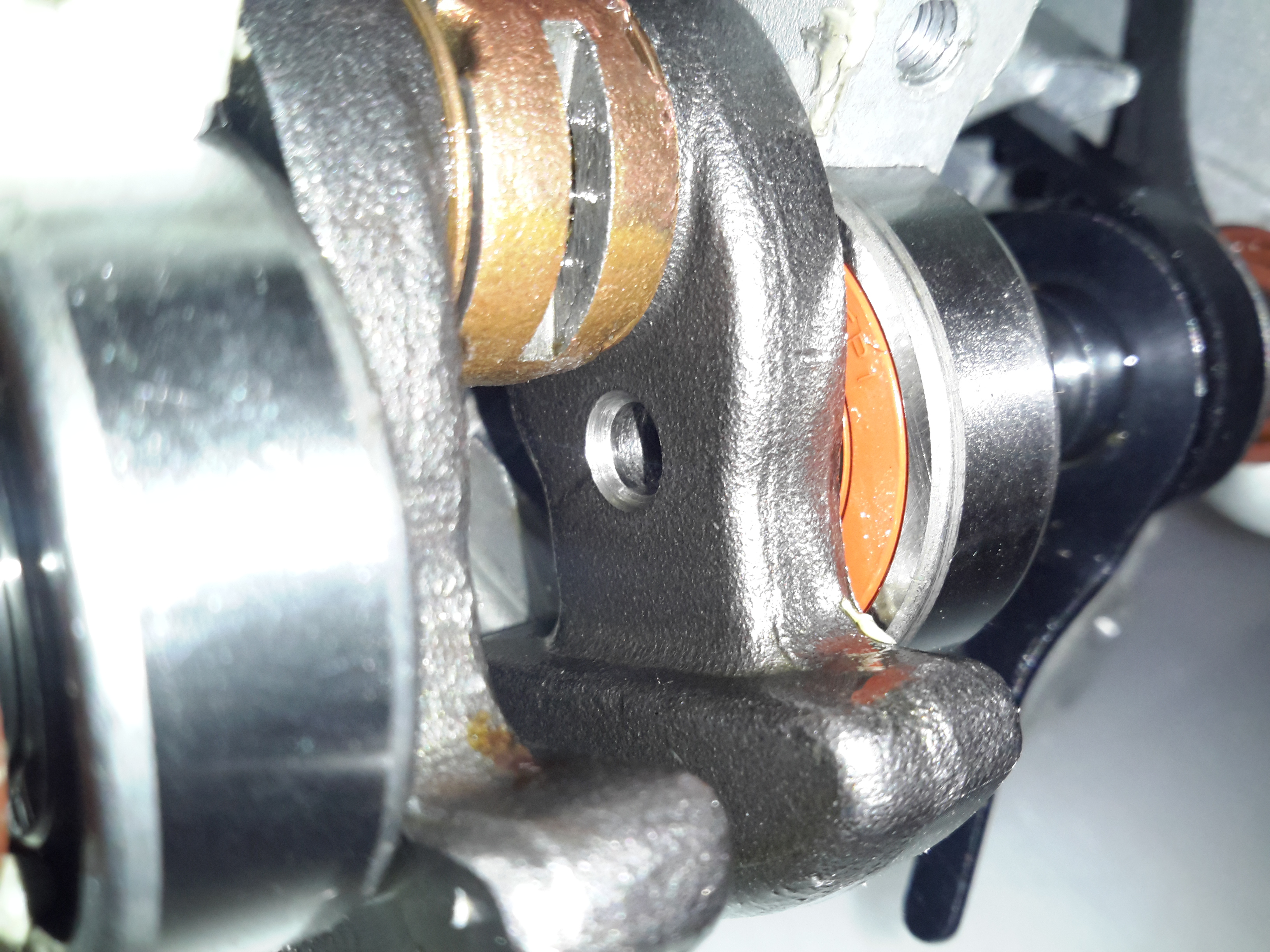
Separating the bottom of the engine was a little difficult, as there is a significant bead of sealant used instead of a gasket. Inside the sump of the engine are a pair of paddles, which stir up the oil into a mist. As the piston moves in the cylinder, it acts as a pump, creating alternating pulses of pressure & vacuum in the crankcase. Oil mist flows through a drilling in the crank from the sump, into the crankcase where it (hopefully) lubricates the bearings & the cylinder wall. Incidentally, the only main bearings are on the crankcase – the far end of the shaft that carries the oil paddles & timing belt is just flapping in the breeze, the only support being the oil seal in the outer housing. The crank itself isn’t hardened – a file easily removes metal from all parts that I could get at. The big end journal pin might be, but these cranks are pressed together so I can’t access that part.
Lubrication Gallery
The oil mist feeds into the crankcase through this hollow section of shaft, there’s a drilling next to the timing belt pulley to connect the two spaces together.
Lower Crankcase
The lower crankcase is just a simple die casting, there’s a check valve at the bottom under the crankshaft to transfer oil to the rocker cover, through the rubber tube on the outside of the engine. After the oil reaches the rocker box, it condenses & returns to the sump via the timing belt cavity.
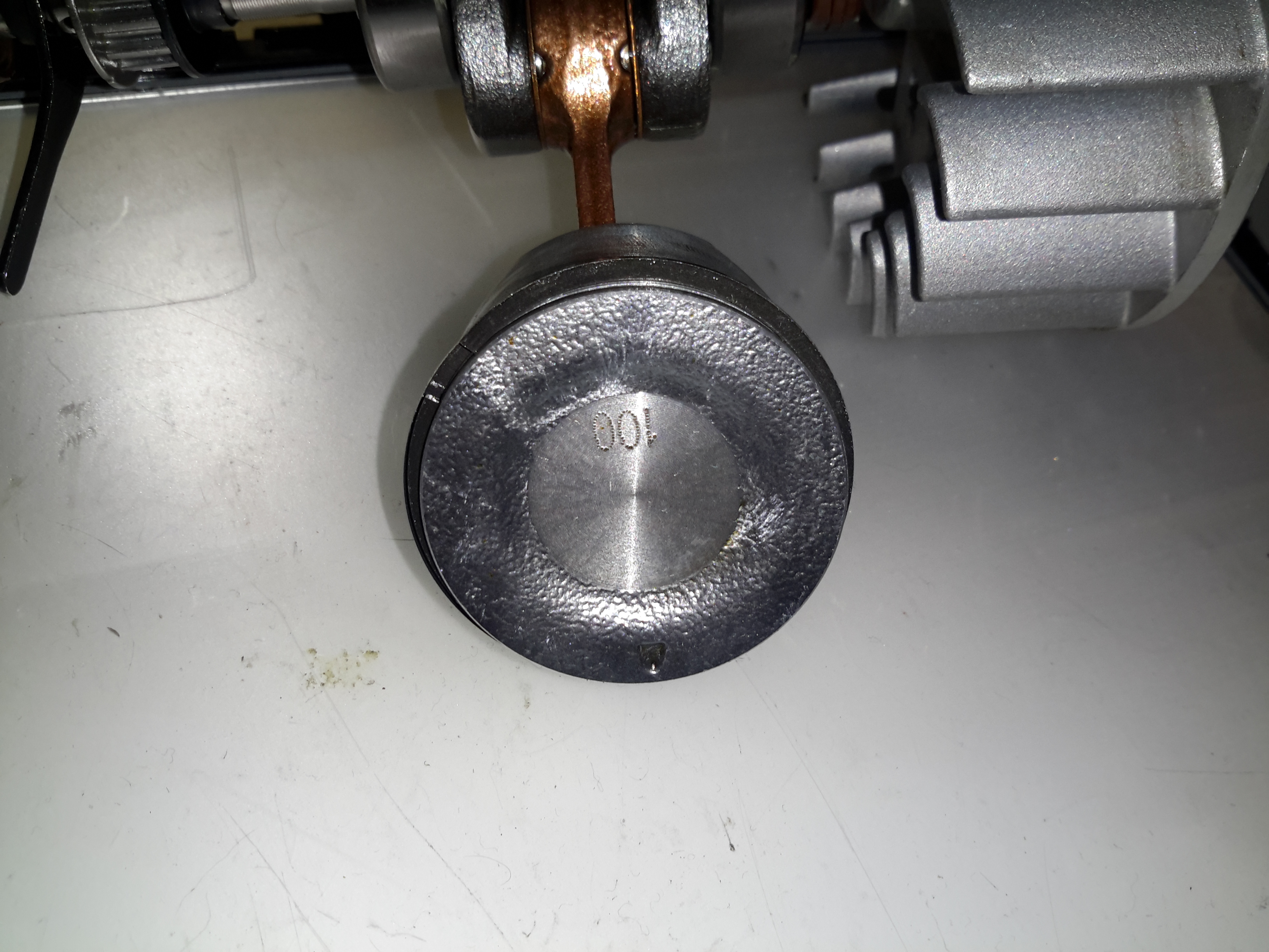
Piston Crown
Removing the crankshaft from the engine block gives me a look at the piston. The factory couldn’t even be arsed to machine the crown, it’s still got the rough finish from the hot-forging press. This bad finish will pick up much carbon from combustion, and would probably cause detonation once enough had accumulated to become incandescent in the heat of combustion. Only the centre is machined, just enough for them to stamp a number on.
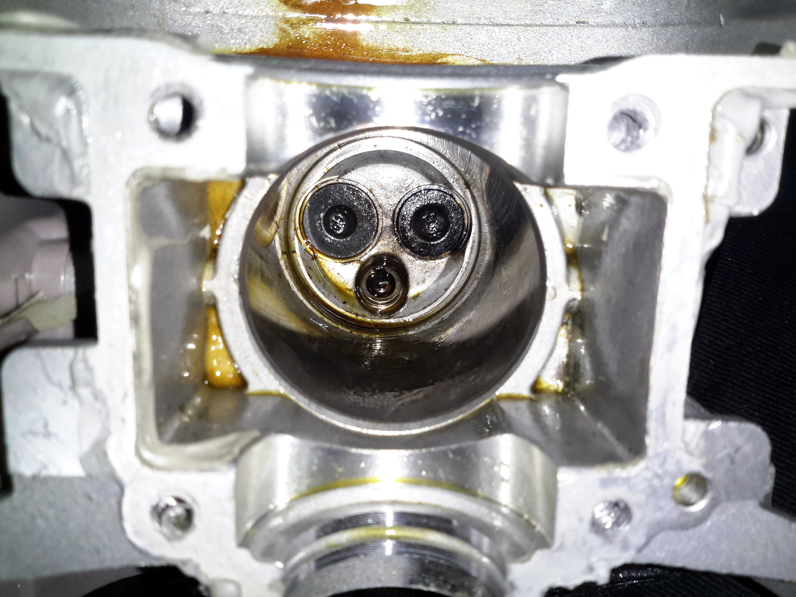
Cylinder Bore
A look up the cylinder bore shows the valves in the cylinder head. These engines, like their 2-stroke cousins have a single casting instead of a separate block & head, so getting at the valves is a little more of a pain. The cylinder bore itself is a cast-in iron liner and it’s totally smooth – like a mirror finish. There’s not a single sign of a crosshatch pattern from honing. If the first engine that died on me was the same – I’d be surprised if it wasn’t, this could easily cause ring breakage. The usual crosshatch pattern the cylinder hone produces holds oil, to better help lubricate the piston & rings. Without sufficient lubrication, the rings will overheat & expand far enough to close the end gap. Once this happens they will break.
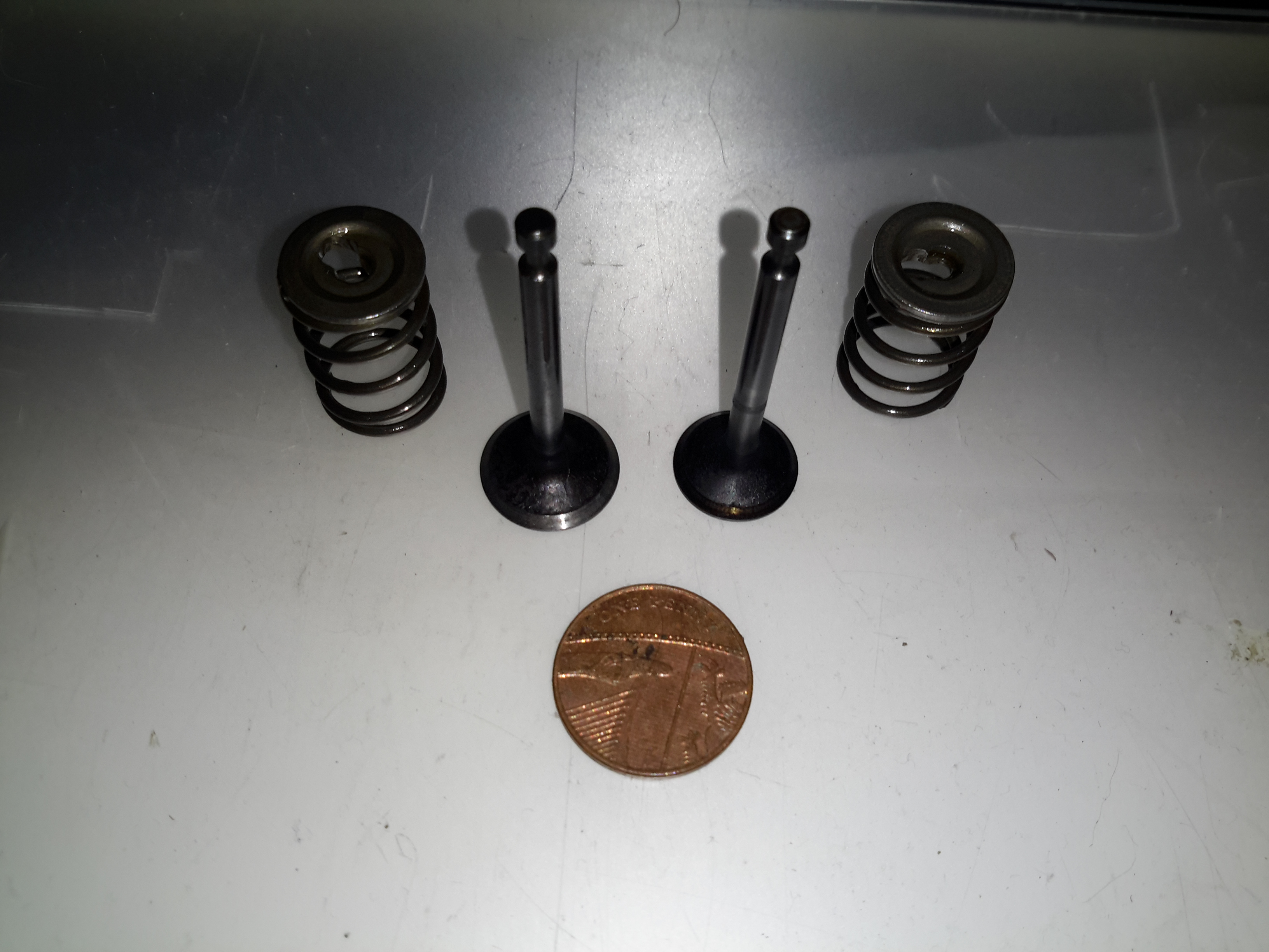
Engine Valves
Finally, here’s the valves with their springs removed from the cylinder. These are the smallest poppet valves I’ve ever seen, a British penny is provided for scale.
In all, these engines share many components with the older 2-stroke versions. The basic crankshaft & connecting rod setup is the same as I’ve seen in many old 2-strokes previous, the addition of the rather ingenious oiling system by Honda is what makes these tiny 4-strokes possible. I definitely won’t be trusting these very cheap copies in any of my projects, reliability is questionable at the least. The apparent lack of cooling air flow over the cylinder from the flywheel fan is concerning, along with the corner-cutting on the cylinder finishing process & piston crown, presumably to reduce factory costs.
I’ve been running my own VPN so I can access my home-based servers from anywhere with an internet connection (not to mention, in this day & age of Government snooping – personal privacy & increased security).
I’m on a pretty quick connection from Virgin Media here in the UK, currently the fastest they offer:
Virgin Media
To do these tests, I used the closest test server to my VPN host machine, in this case Paris. This keeps the variables to a minimum. Testing without the VPN connection gave me this:
Paris Server Speed
I did expect a lower general speed to a server further away, this will have much to do with my ISP’s traffic management, network congestion, etc. So I now have a baseline to test my VPN throughput against.
The problem I’ve noticed with OpenVPN stock configs are that the connections are painfully slow – running over UDP on the usual port of 1194 the throughput was pretty pathetic:
Stock Config Speed
I did some reading on the subject, the first possible solution being to change the send/receive buffers so they’re set to a specific value, rather than letting the system handle them. I also added options to get the server to push these values to the clients, this saving me the trouble of having to reissue all the client configurations.
Unfortunately just this option didn’t work as well as I’d like, downstream speeds jumped to 25Mb/s. In the stock config, the tunnel MTU & MSSFIX settings aren’t bothered with, some adjustment to set the tunnel MTU to lower than the host link MTU (in my case the standard 1500) prevents packet fragmentation, MSSFIX let’s the client TCP sessions know to limit the packet sizes it sends so that after OpenVPN has done the encryption & encapsulation, the packets do not exceed the set size. This also helps prevent packet fragmentation.
tun-mtu 1400
mssfix 1360
VPN Tweaked
After adjusting these settings, the download throughput over the VPN link has shot up to 136Mb/s. Upload throughput hasn’t changed as this is limited by my connection to Virgin Media. Some more tweaking is no doubt possible to increase speeds even further, but this is fine for me at the moment.
Here’s the other TV that was picked up from the local water point having been put of to be recycled. This one is much newer than the Thorn TV, a 10″ colour version from Ferguson.
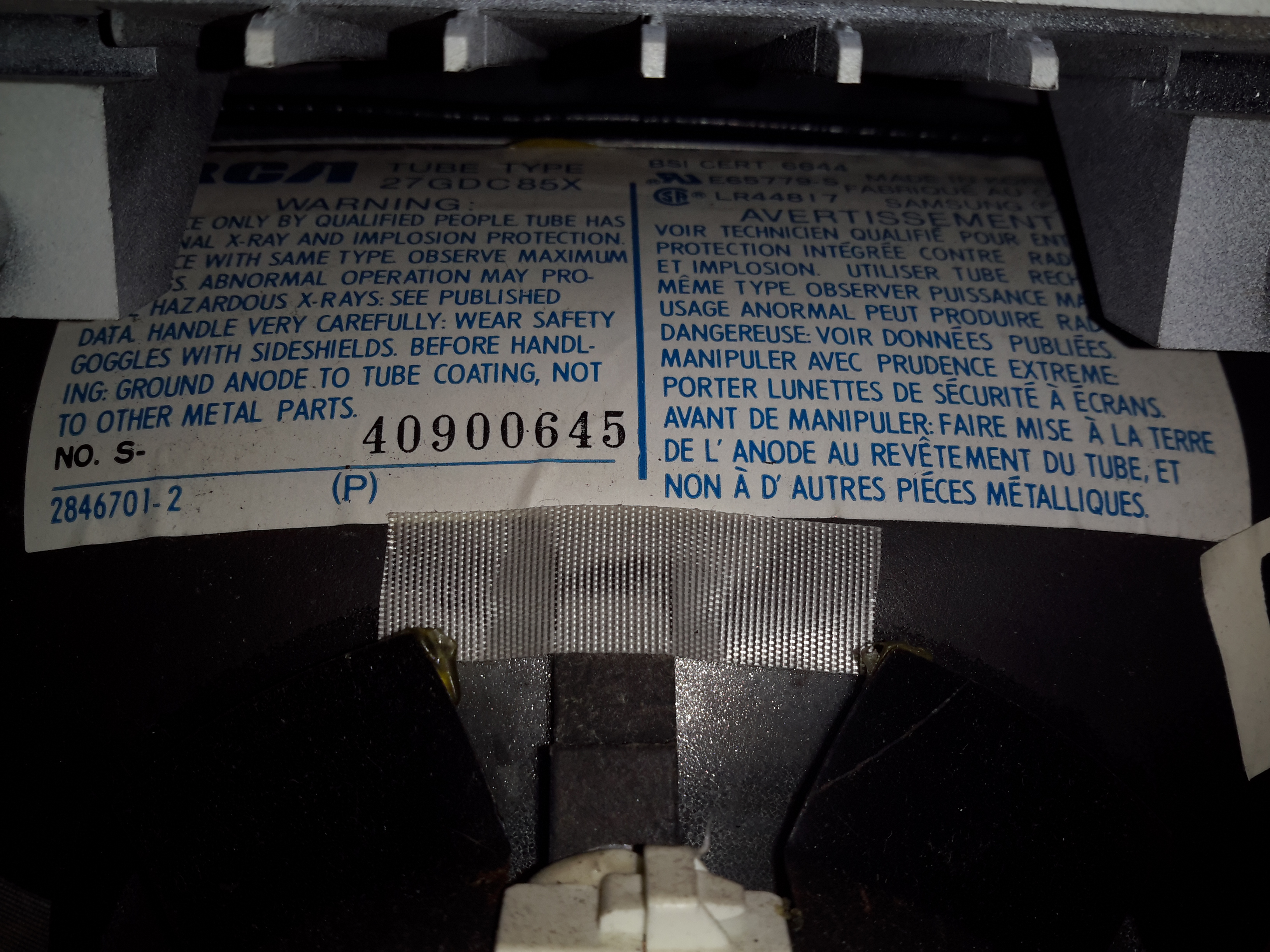
RCA 27GDC85X CRT
The colour CRT used is an RCA branded one, 27GDC85X.
Power Inputs
Like the other TV, this one is dual voltage input, mains 240v & 12v battery. This TV is a factory conversion of a standard 240v AC chassis though.
HV PSU
The 12v power first goes into this board, which looked suspiciously like an inverter. Measuring on the output pins confirmed I was right, this addon board generates a 330v DC supply under a load, but it’s not regulated at all, under no load the output voltage shoots up to nearly 600v!
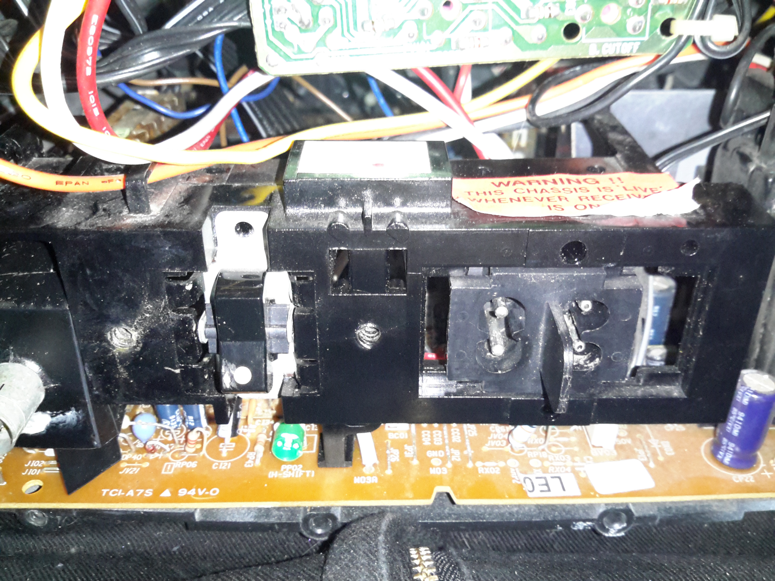
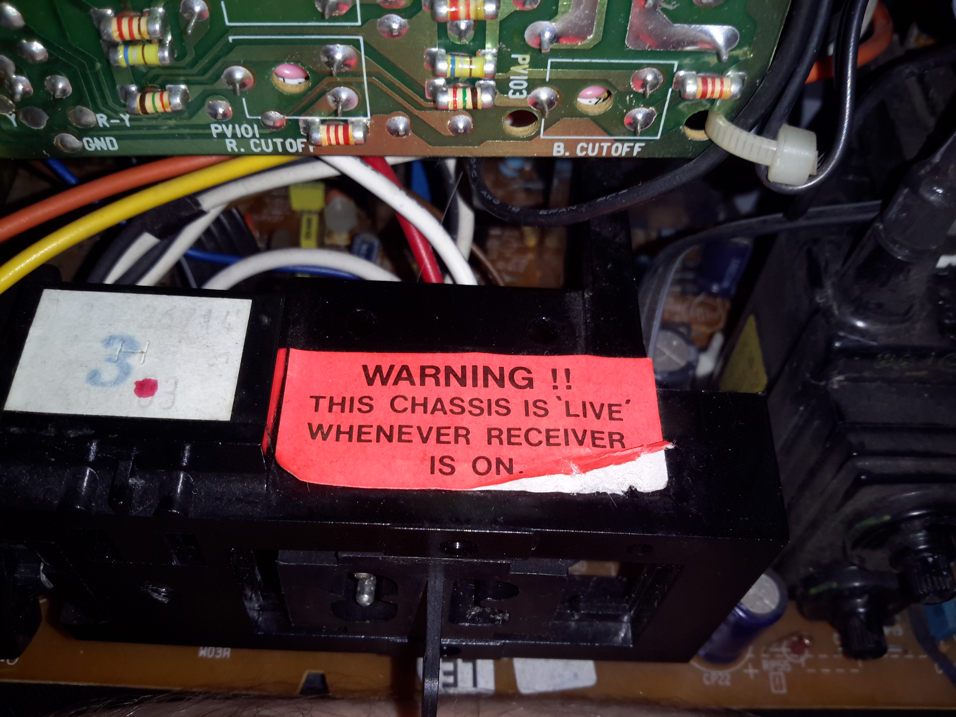
Live Chassis
I’ve not seen one of these labels on a TV for many years, when back in the very old TV sets the steel chassis would be used to supply power to parts of the circuitry, to save on copper. Although it doesn’t have a metal chassis to actually become live, so I’m not sure why it’s here.
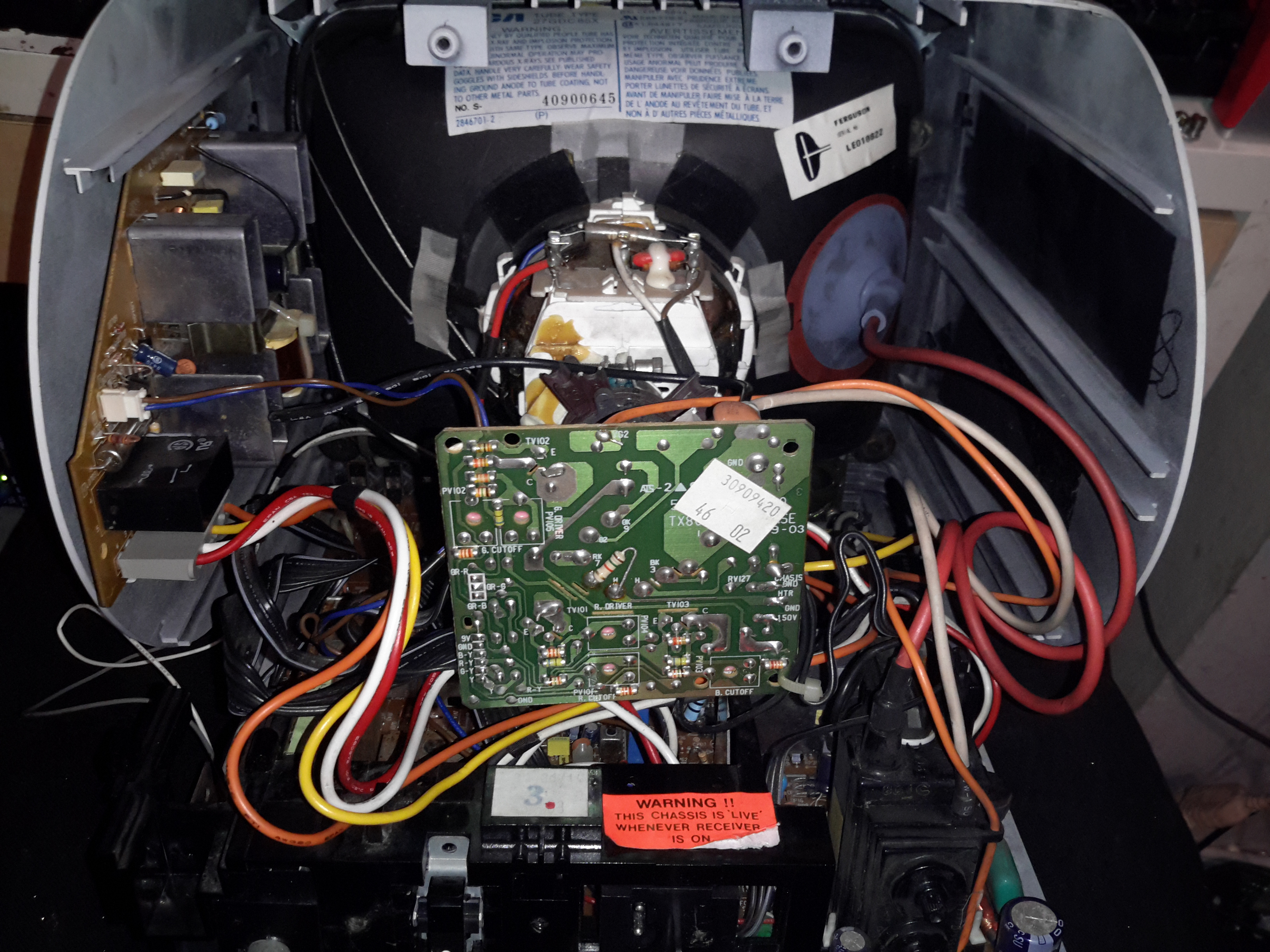
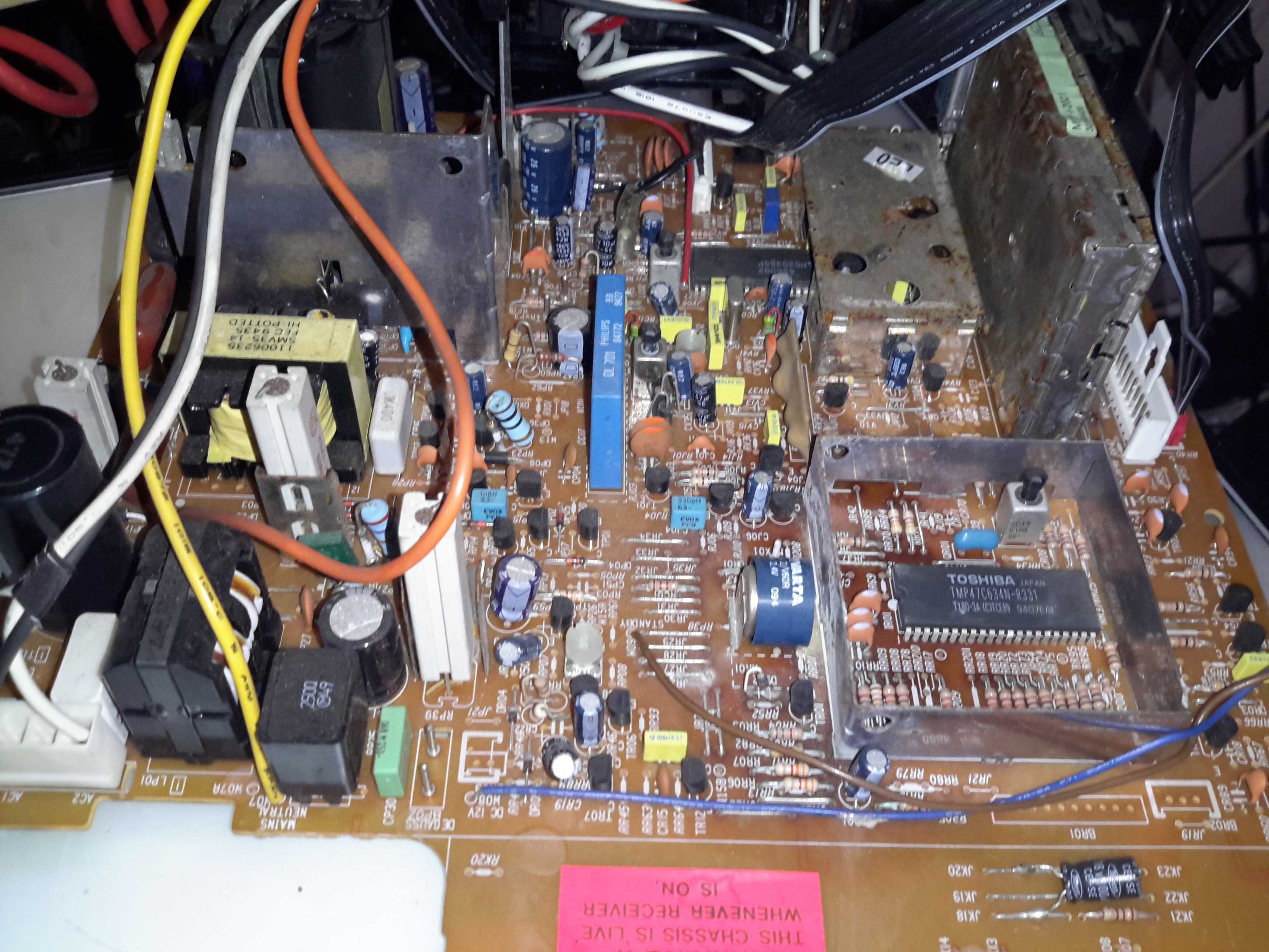
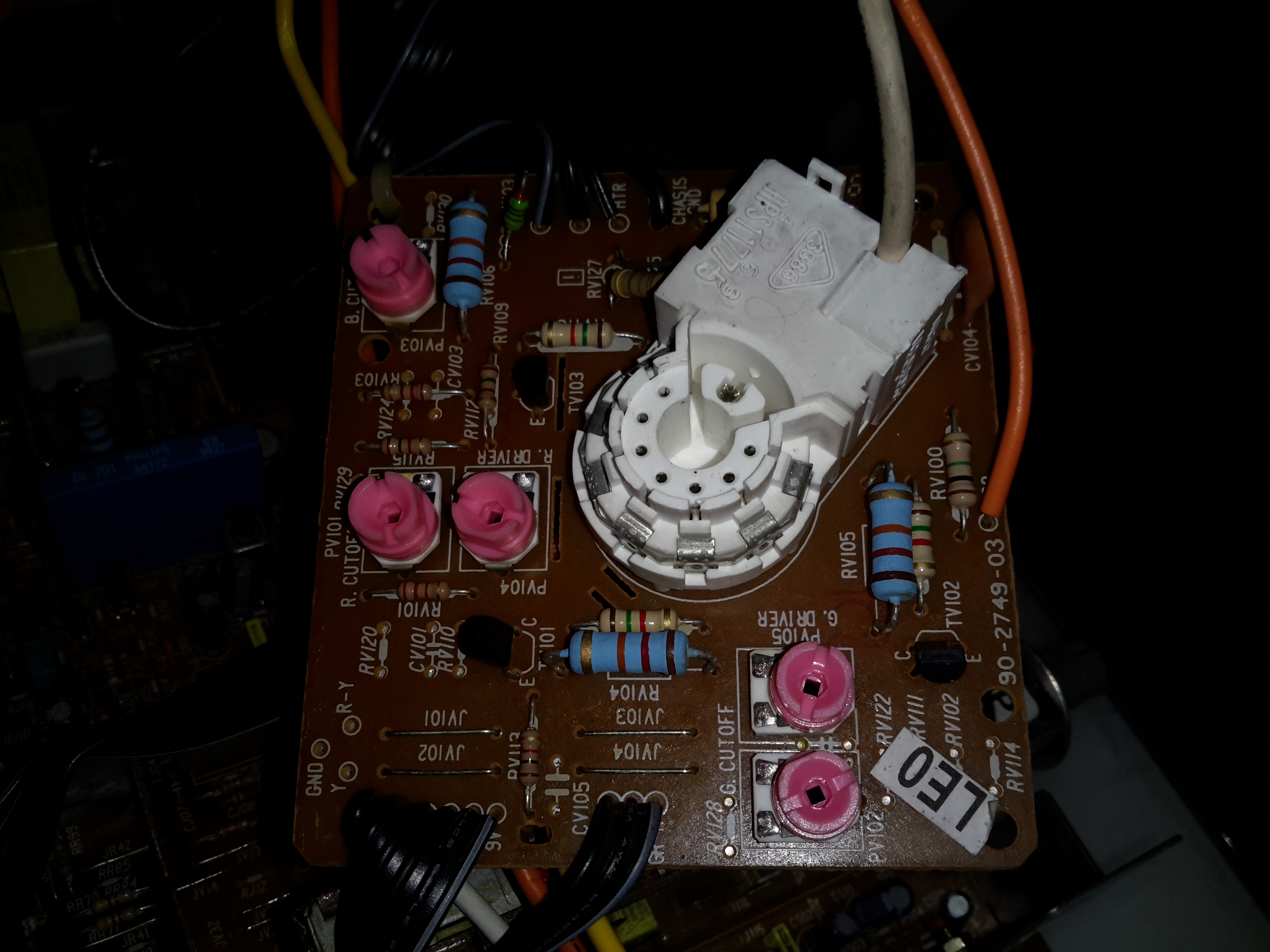
Main PCB
The main PCB is much more integrated in this newer TV, from the mid 90’s, everything is pretty much taken care of by silicon by this point.
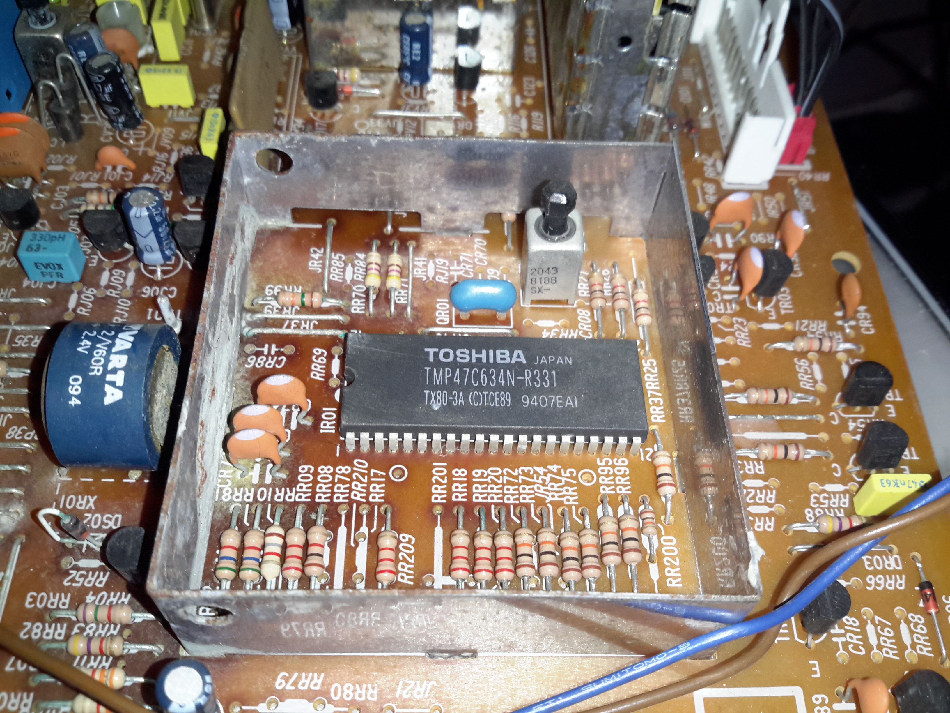
Main Microcontroller
This Toshiba µC takes care of channel switching & displaying information on the CRT. The tuner in this TV is electronically controlled.
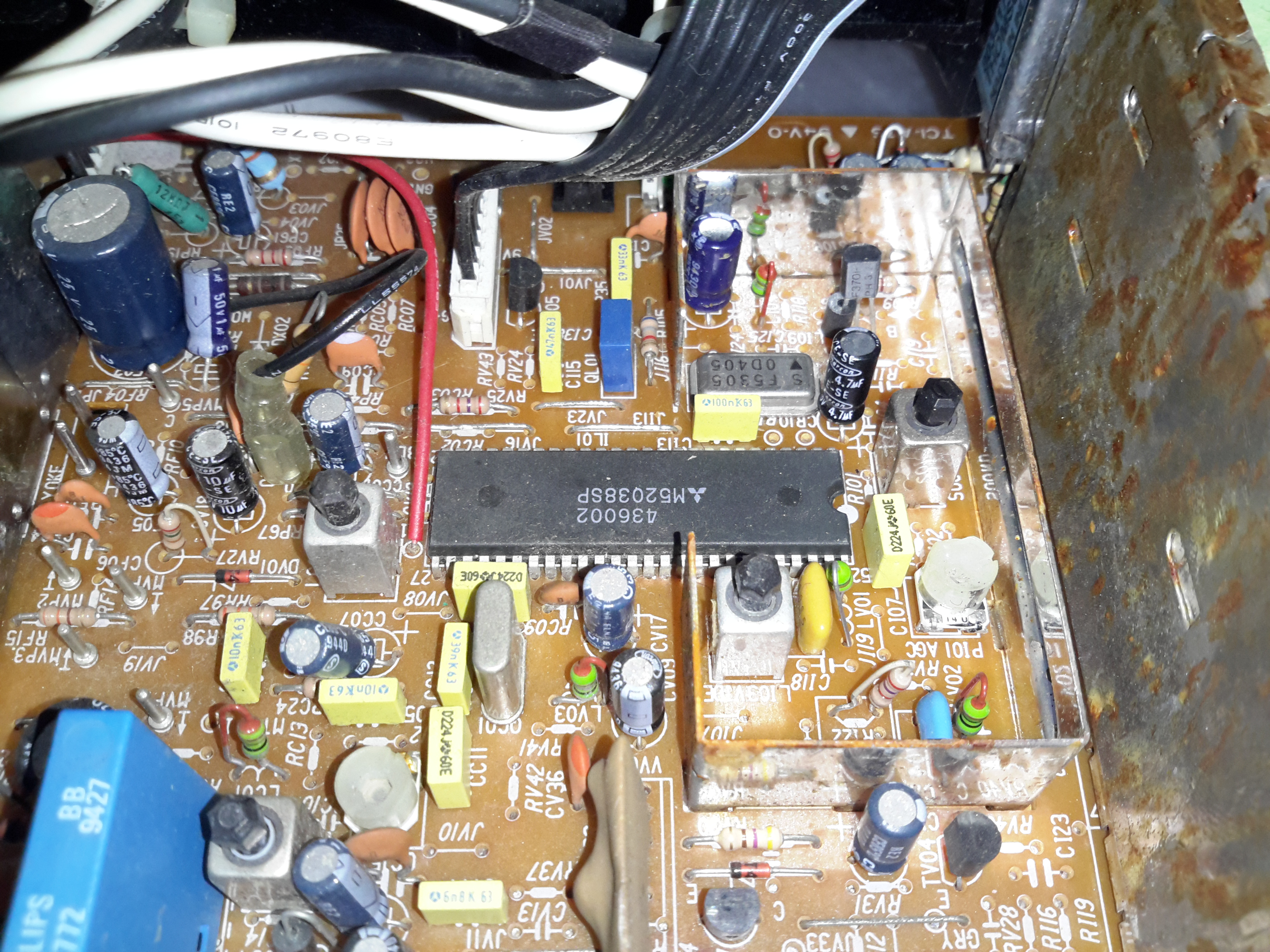
PAL Signal Processor
The video signal is handled by this Mitsubishi IC, which is a PAL Signal Processor, this does Video IF, Audio IF, Chroma, & generates the deflection oscillators & waveforms to drive the yoke.
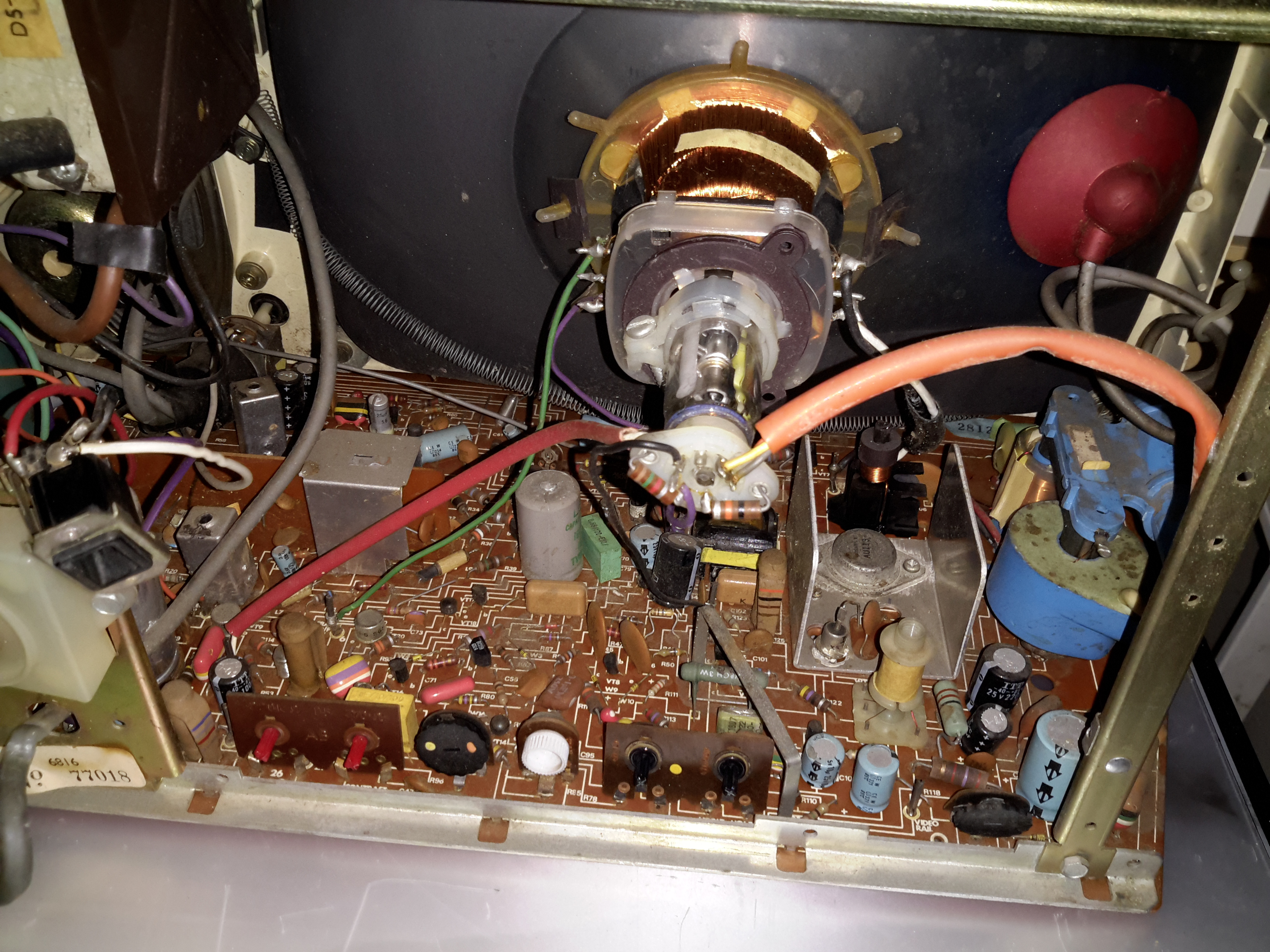
CRT Adjustments
There are some adjustments on the CRT neck board for RGB drive levels & cutoff levels. This board also had the final video amplifiers onboard, which drive the CRT cathodes.
The other day at the local canal-side waterpoint, this TV was dumped for recycling, along with another later model Colour TV. This is a 1970’s Black & White mains/battery portable made by Thorn. It’s based on a common British Radio Corporation 1590 chassis. Having received a soaking from rain, I didn’t expect this one to work very well.
Tuner
Being so old, there is no electronic control of the tuner in this TV, and only has the capability to mechanically store 4 different channels. The tuner itself is a cast box with a plastic cover.
Tuning Lever
The mechanical buttons on the front of the TV push on this steel bar, by different amounts depending on the channel setting. This bar is connected to the tuning capacitor inside the tuner.
Tuner Compartments
Unclipping the plastic cover, with it’s lining of aluminium foil for shielding reveals the innards of the tuner module.
Tuner Input Stage
Here’s the tuner front end RF transistor, which has it’s can soldered into the frame, this is an AF239 germanium UHF transistor, rated at up to 900MHz.
Tuner IF Mixer Stage
As the signal propagates through the compartments of the tuner, another transistor does the oscillator / IF mixing, an AF139 germanium, rated to 860MHz.
Tuning Capacitor
As the buttons on the front of the set are pushed, moving the lever on the outside, the tuning capacitor plates intermesh, changing the frequency that is filtered through the tuner. The outer blades of the moving plates are slotted to allow for fine tuning of the capacitance, and therefore transmitted frequency by bending them slightly.
Mains Transformer
Being a dual supply TV that can operate on either 12v battery power or mains, this one has a large centre tapped mains transformer that generates the low voltage when on AC power. Full wave rectification is on the main PCB. The fuse of this transformer has clearly been blown in the past, as it’s been wound with a fine fuse wire around the outside to repair, instead of just replacing the fuse itself.
Chassis Rear
The back of the set has all the picture controls on the bottom edge, with the power input & antenna connections on the left just out of shot. The CRT in this model is an A31-120W 12″ tube, with a really wide deflection angle of 110°, which allows the TV to be smaller.
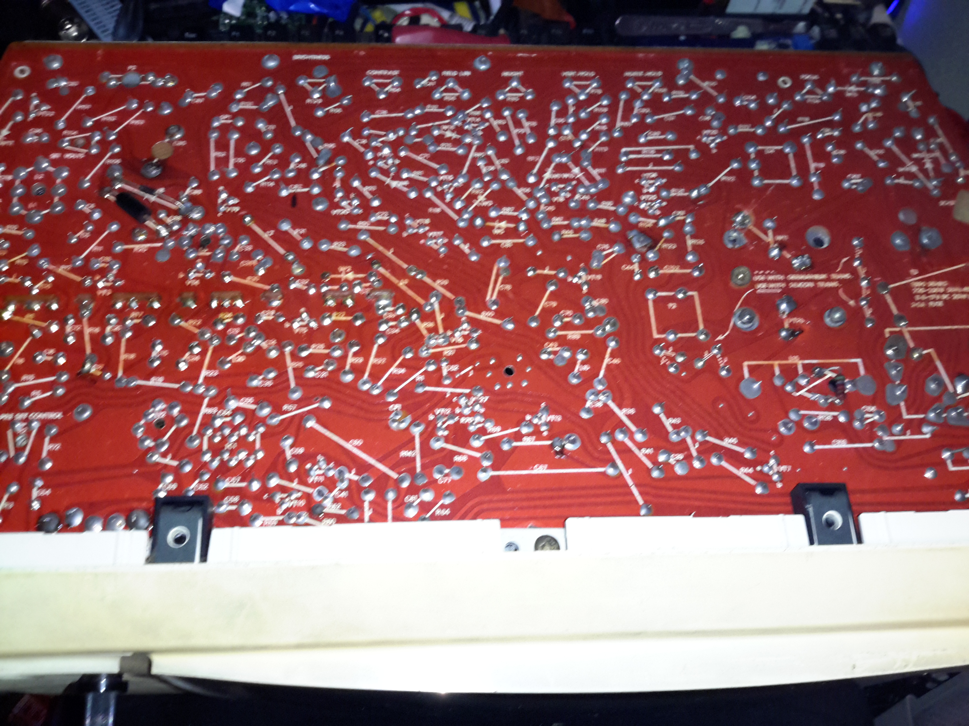
Main PCB
The bottom of the mainboard has all the silkscreen markings for the components above which certainly makes servicing easier 😉 This board’s copper tracks would have been laid out with tape, obviously before the era of PCB design software.
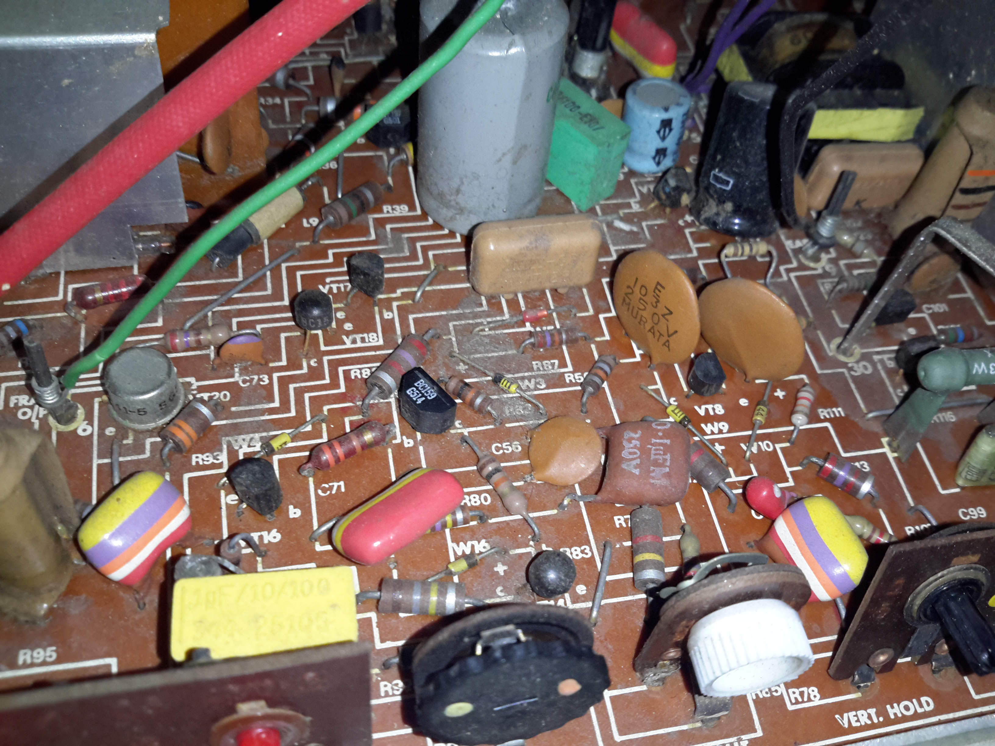
Components
The components on this board are laid out everywhere, not just in square grids. The resistors used are the carbon composition type, and at ~46 years old, they’re starting to drift a bit. After measuring a 10K resistor at 10.7K, all of these would need replacing I have no doubt. Incedentally, this TV could be converted to take a video input without the tuner, by lifting the ferrite beaded end of L9 & injecting a signal there.
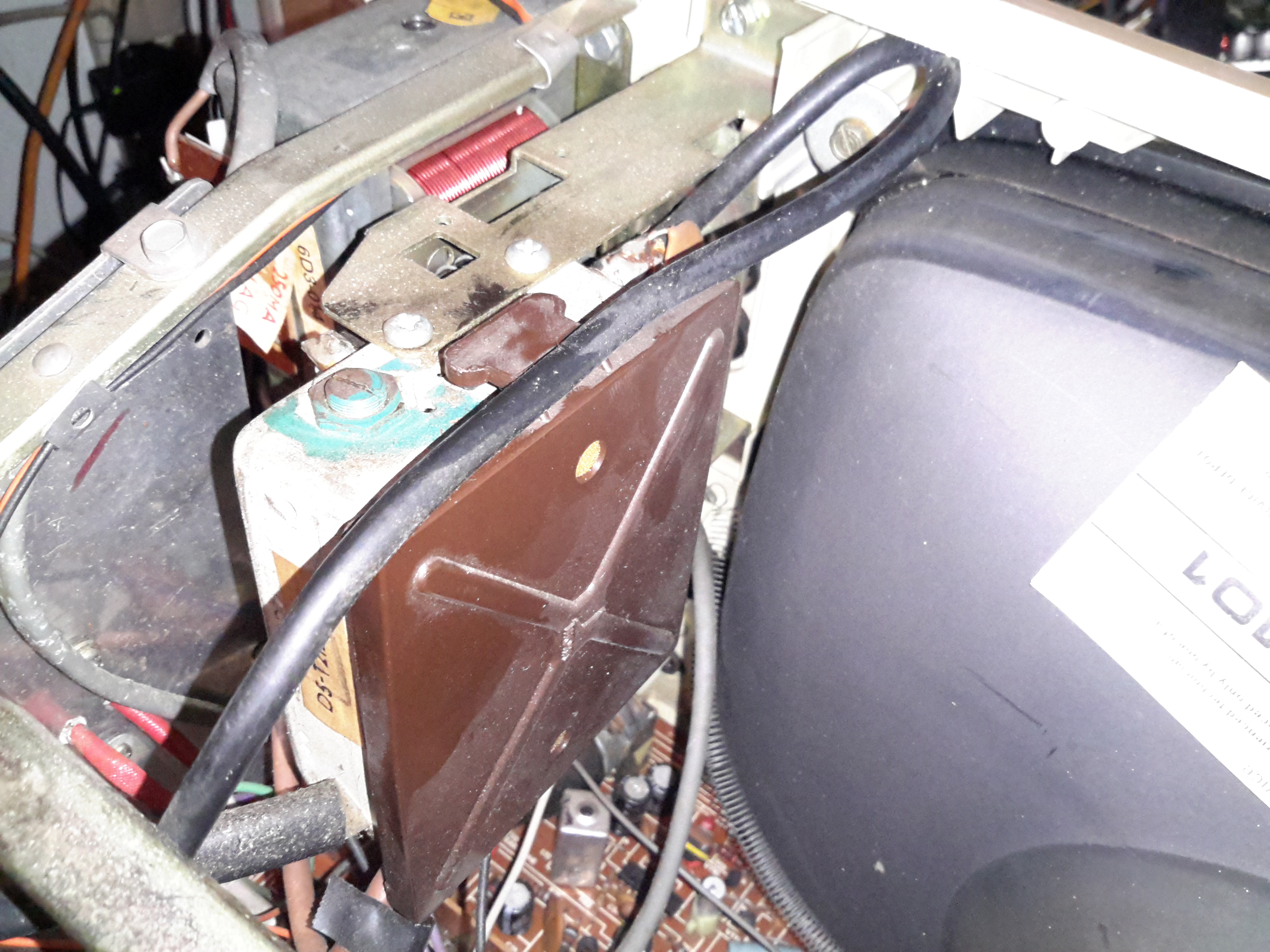
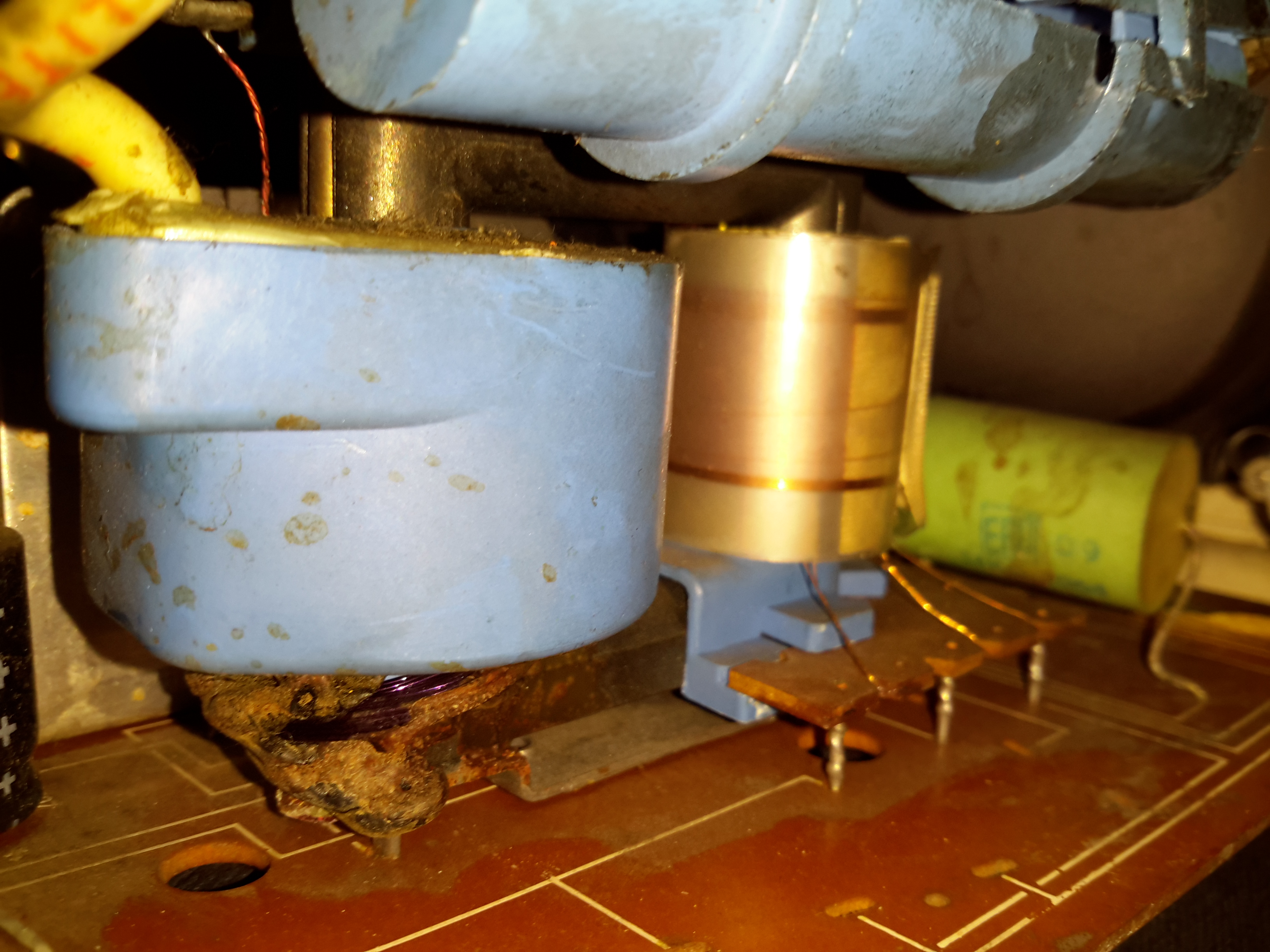
Flyback Primary Windings
The flyback (Line Output Transformer) is of the old AC type, with the rectifier stack on top in the blue tube, as opposed to more modern versions that have everything potted into the same casing. The primary windings are on the other leg of the ferrite core, making these transformers much more easily repairable. This transformer generates the 12kV required for the CRT final anode, along with a few other voltages used in the TV, for focussing, etc.
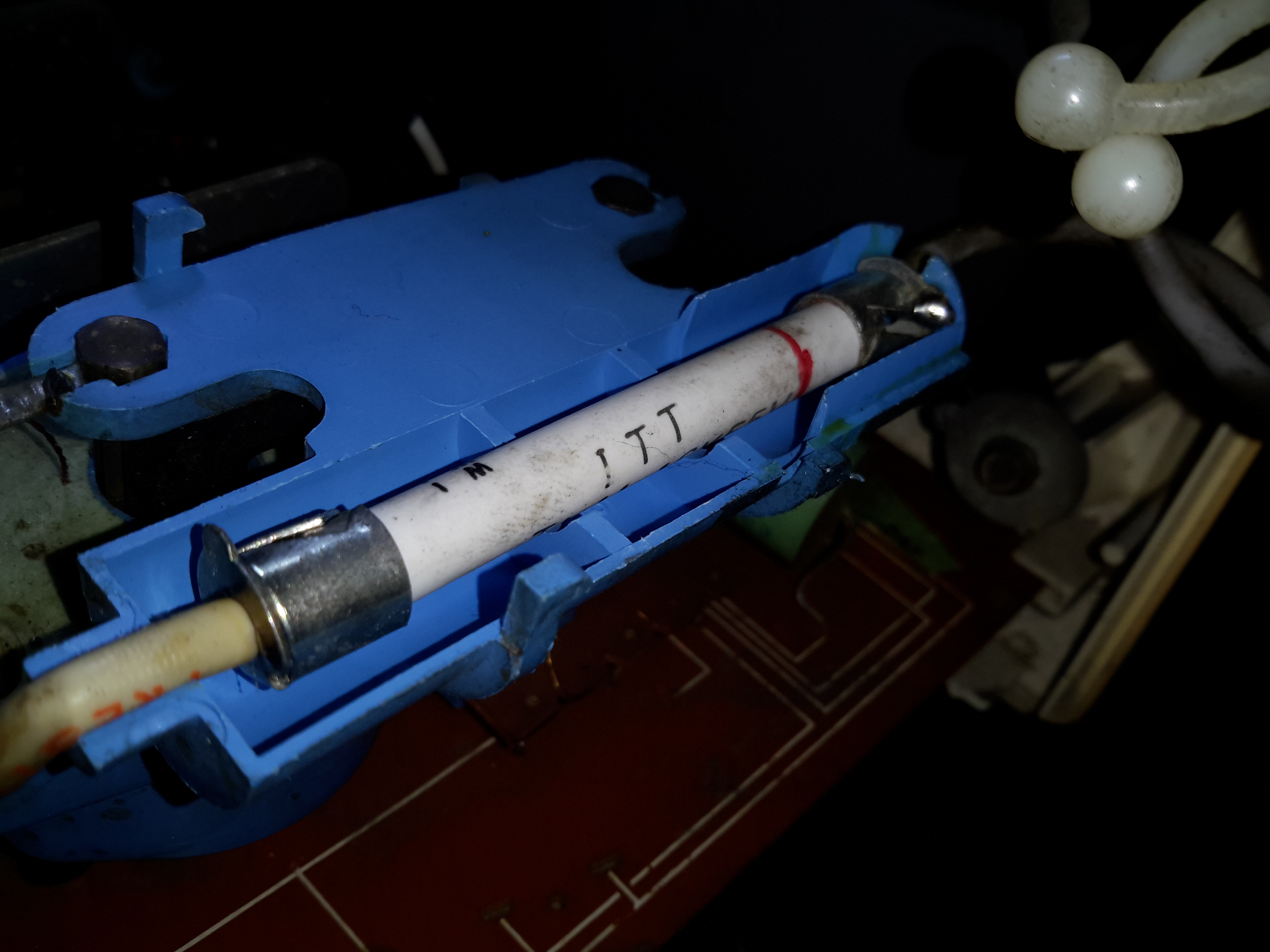
Rectifier Stack
The main EHT rectifier stack looks like a huge fuse, inside the ceramic tube will be a stack of silicon diodes in series, to withstand the high voltage present.
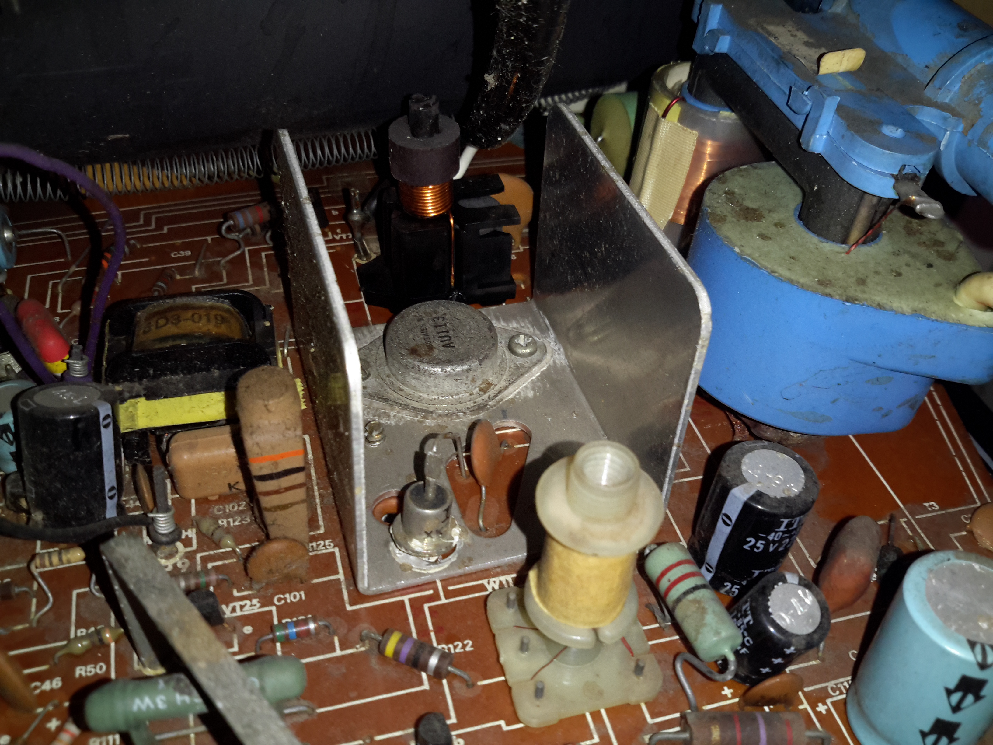
Horizontal Output Transistor
This is the main switching transistor that drives the flyback, the HOT. This is an AU113, another germanium type, rated at 250v 4A. The large diode next to the transistor is the damper.
I’ve managed to find all the service information for this set online, link below!
[download id=”5616″]
More to come if I manage to get this TV working!
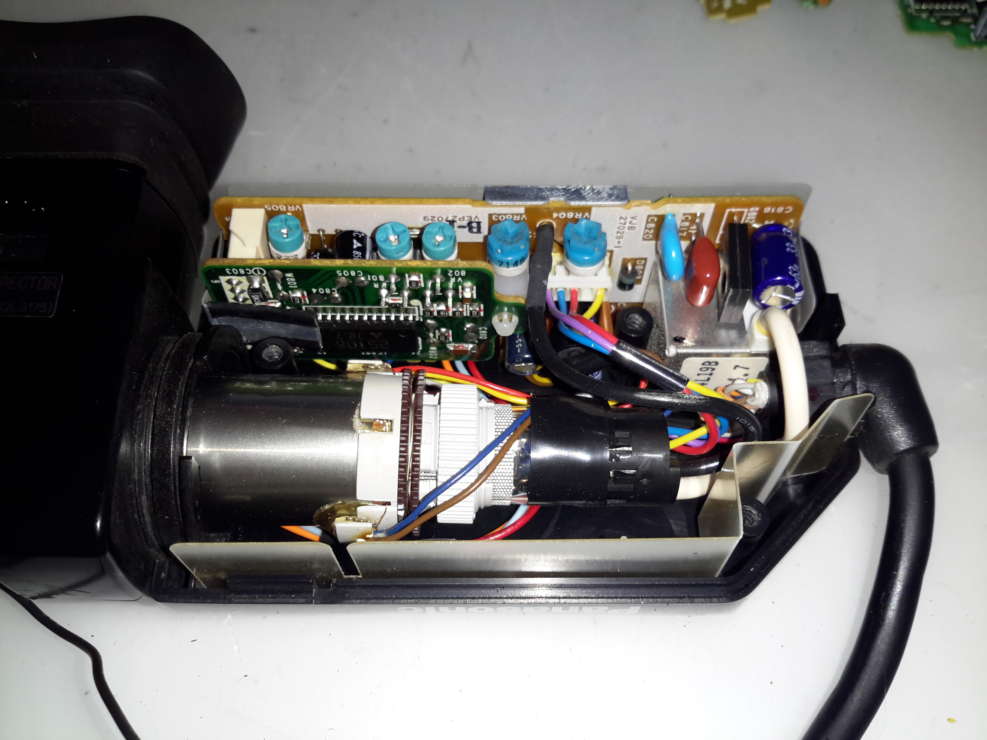
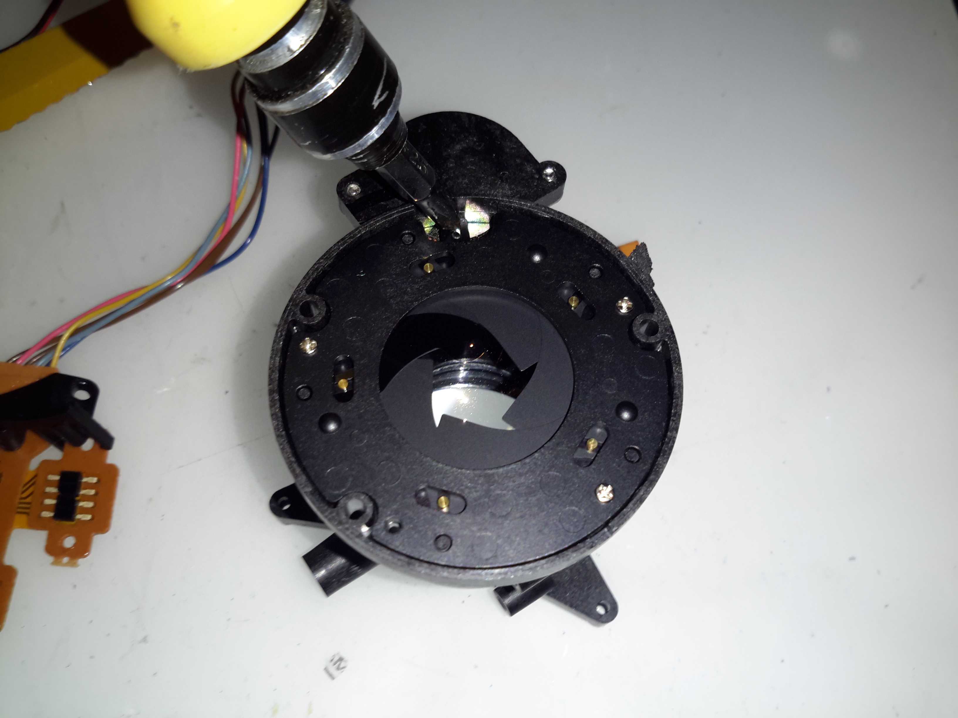
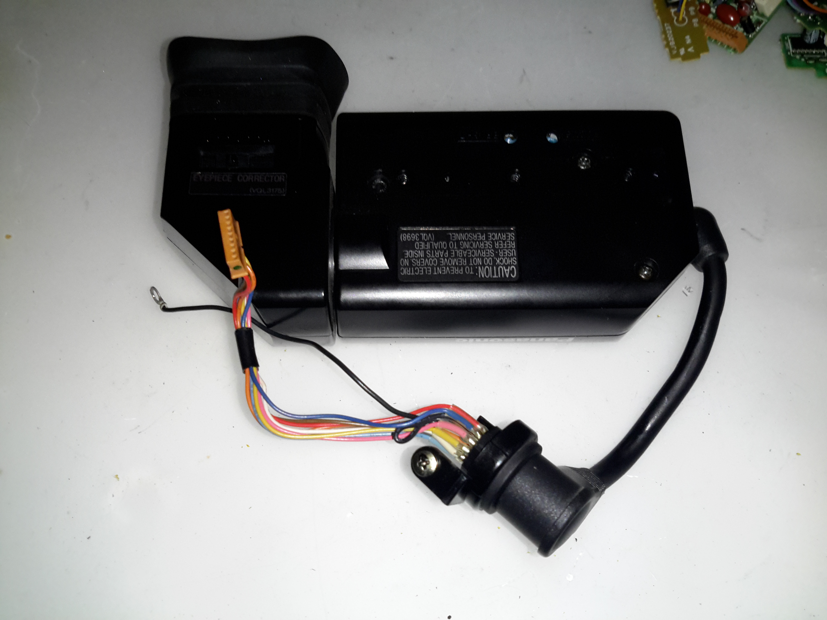
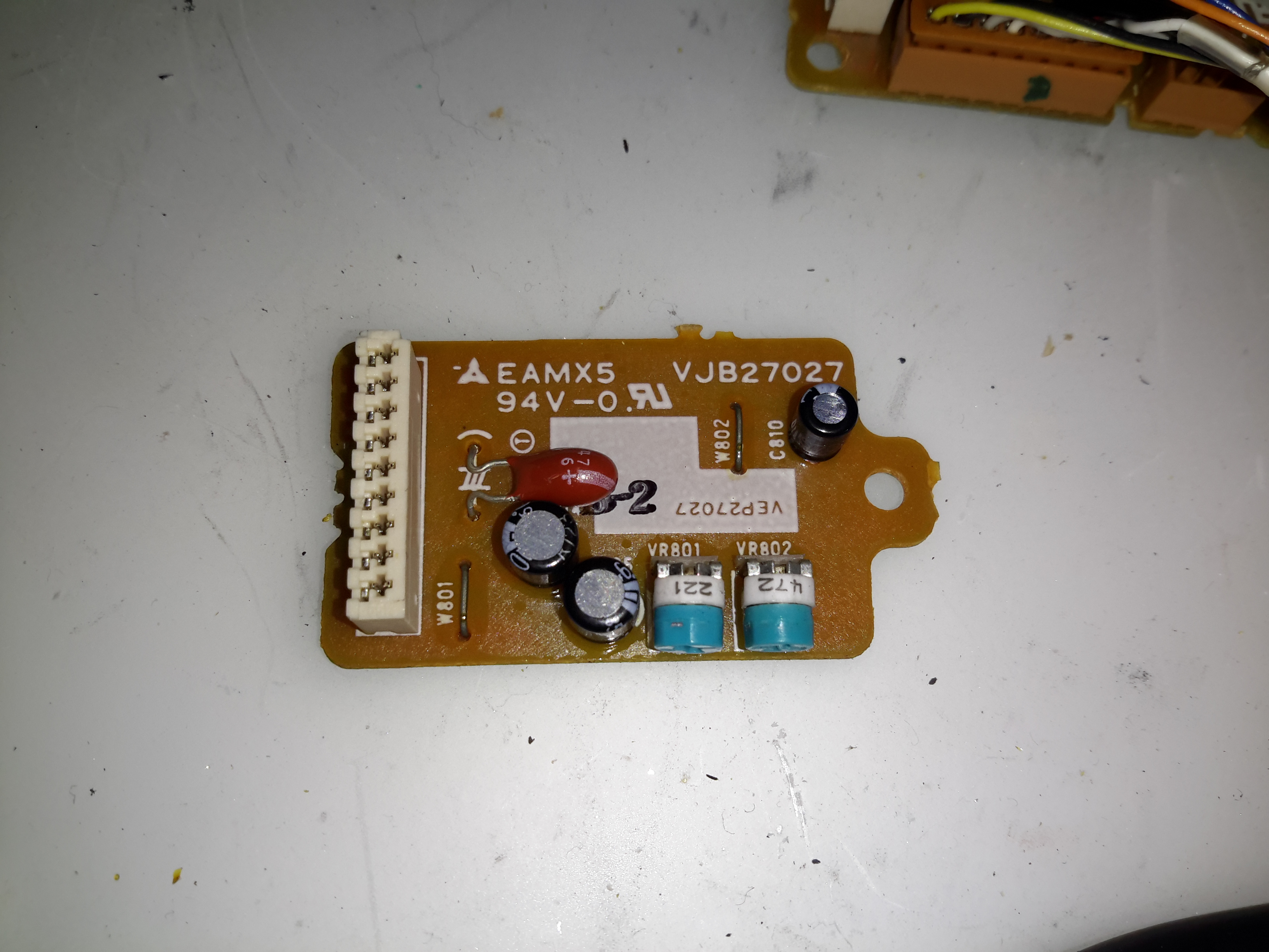
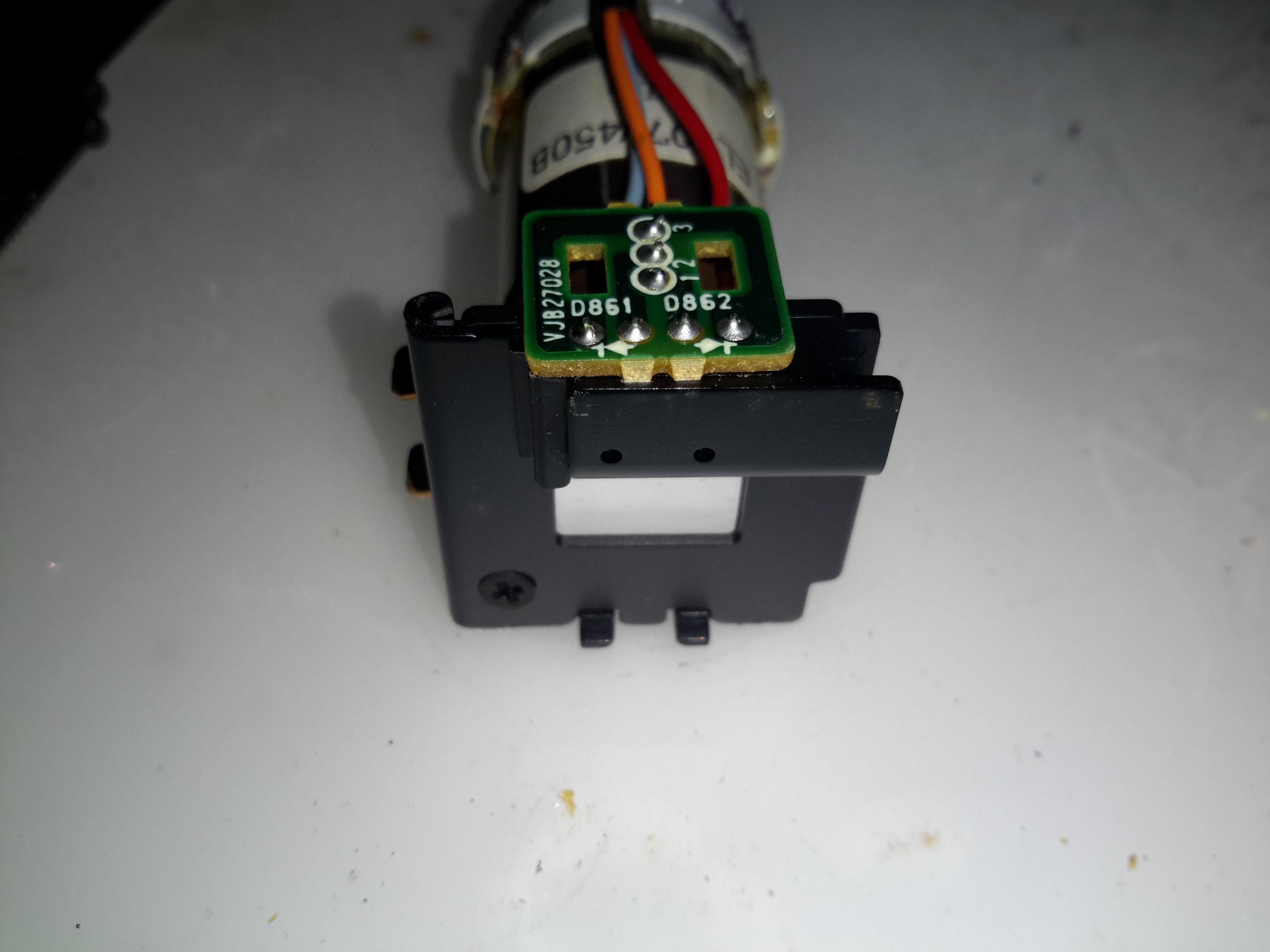
The old Panasonic NV-M5 has the standard for the time CRT based viewfinder assembly, which will happily take a composite video signal from an external source.
This viewfinder has many more connections than I would have expected, as it has an input for the iris signal, which places a movable marker on the edge of the display. This unit also has a pair of outputs for the vertical & horizontal deflection signals, I imagine for sync, but I’ve never seen these signals as an output on a viewfinder before.
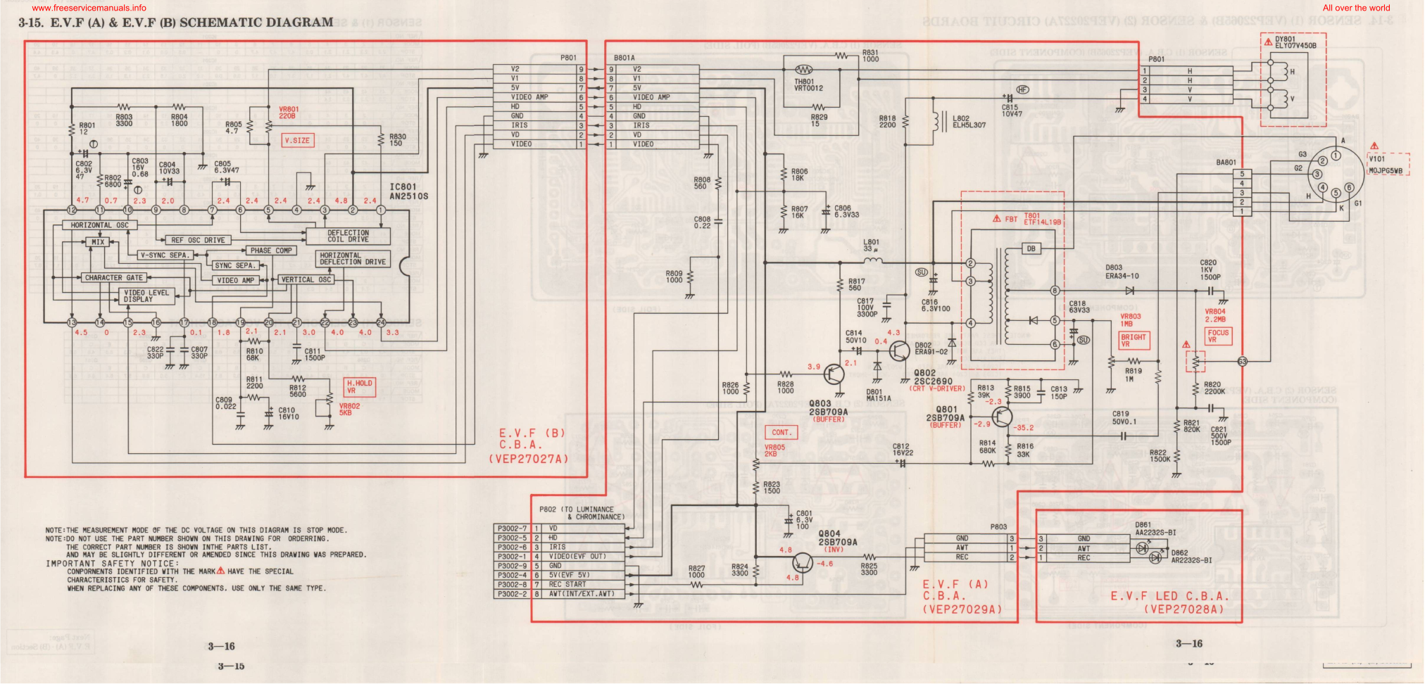
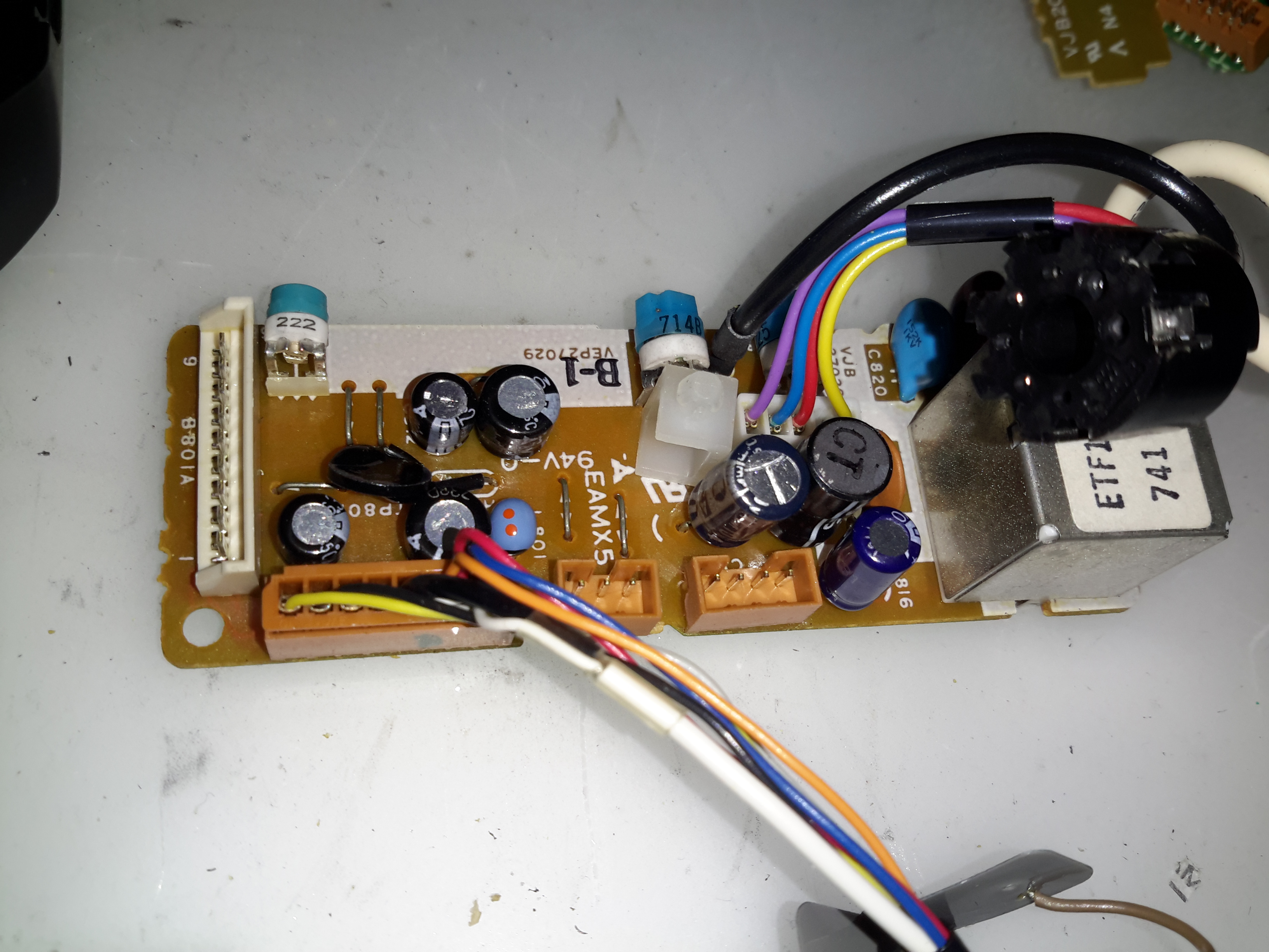
EVF Schematic
Luckily I managed to get a service manual for the camera with a full schematic.
This unit takes a 5v input, as opposed to the 8-12v inputs on previous cameras, so watch out for this! There’s also no reverse polarity protection either.
Pins
Making the iris marker vanish from the screen is easy, just put a solder bridge between pins 15 & 16 of the drive IC. The important pins on the interface connector are as follows:
Pin 3: GND
Pin 4: Video Input
Pin 5: Video GND
Pins 6: +5v Supply
I was recently given this unit, along with another Behringer sound processor to repair, as the units were both displaying booting problems. This first one is a rather swish Mastering Processor, which has many features I’ll leave to Behringer to explain 😉
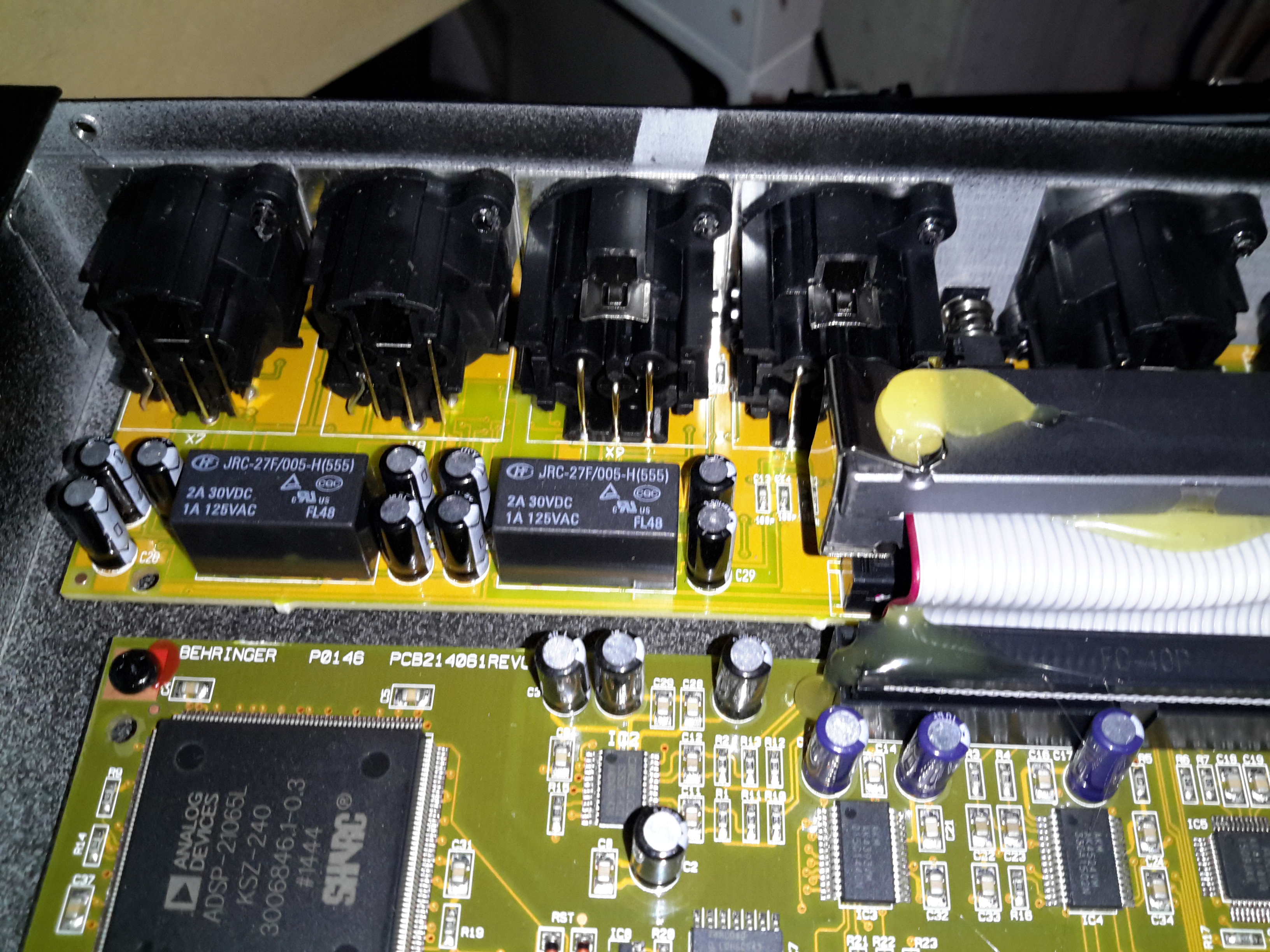
Input Board & Relays
All the inputs are on the back of this 19″ rackmount bit of kit, nothing much on this PCB other than the connectors & a couple of switching relays.
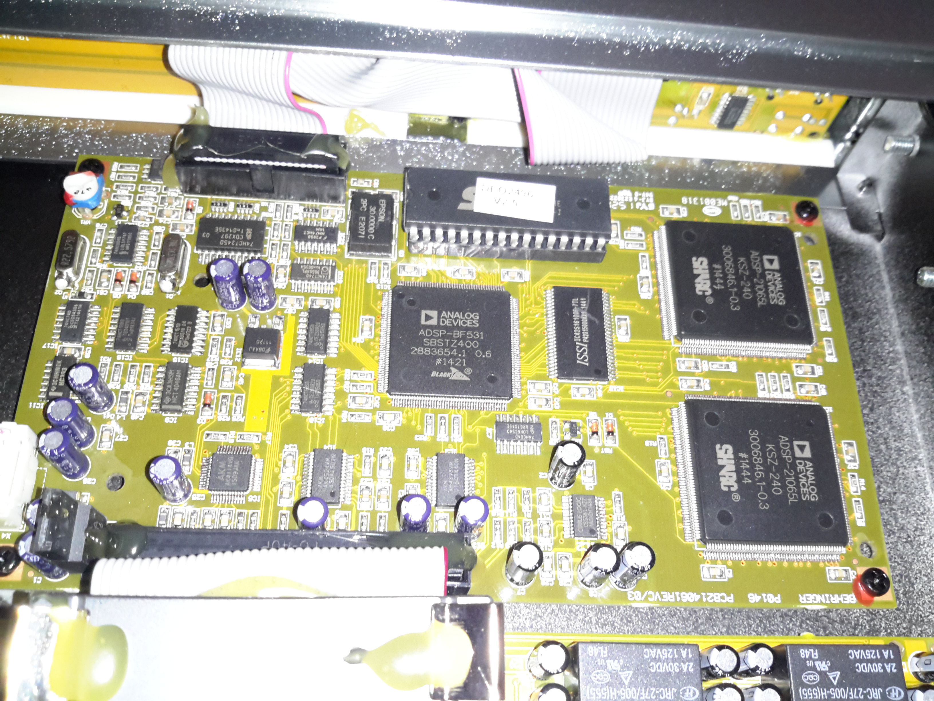
Main Processor PCB
All the magic is done on the main processor PCB, which is host to 3 Analog Devices DSP processors:
ADSP-BF531 BlackFin DSP. This one is probably handling most of the audio processing, as it’s the most powerful DSP onboard at 600Mhz. There’s a ROM on board above this for the firmware & a single RAM chip. On the right are a pair of ADSP-21065 DSP processors at a lower clock rate of 66MHz. To the left is some glue logic to interface the user controls & dot-matrix LCD.
PSU Module
The PSU in this unit is a pretty standard looking SMPS, with some extra noise filtering & shielding. The main transformer is underneath the mu-metal shield in the centre of the board.
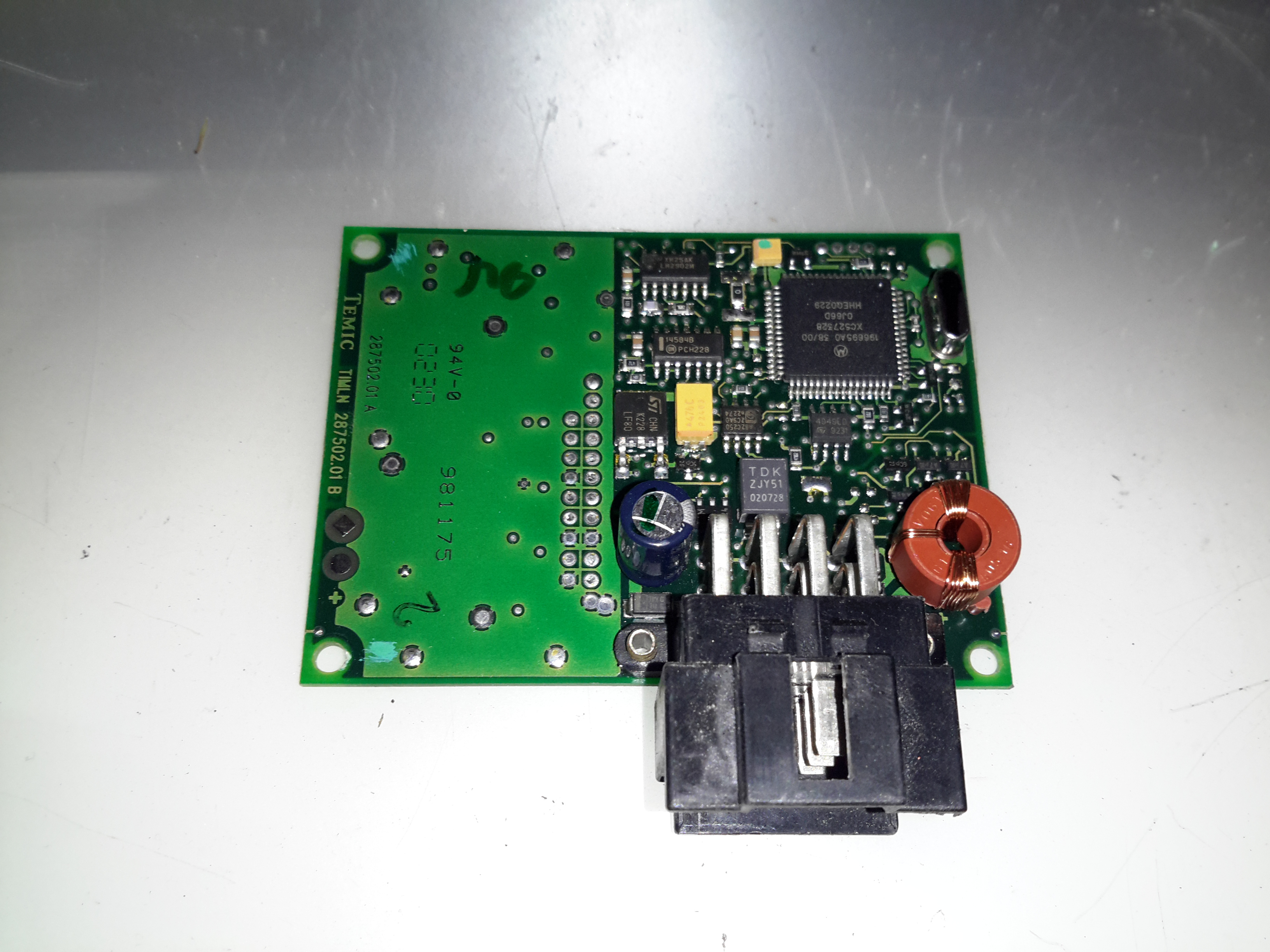
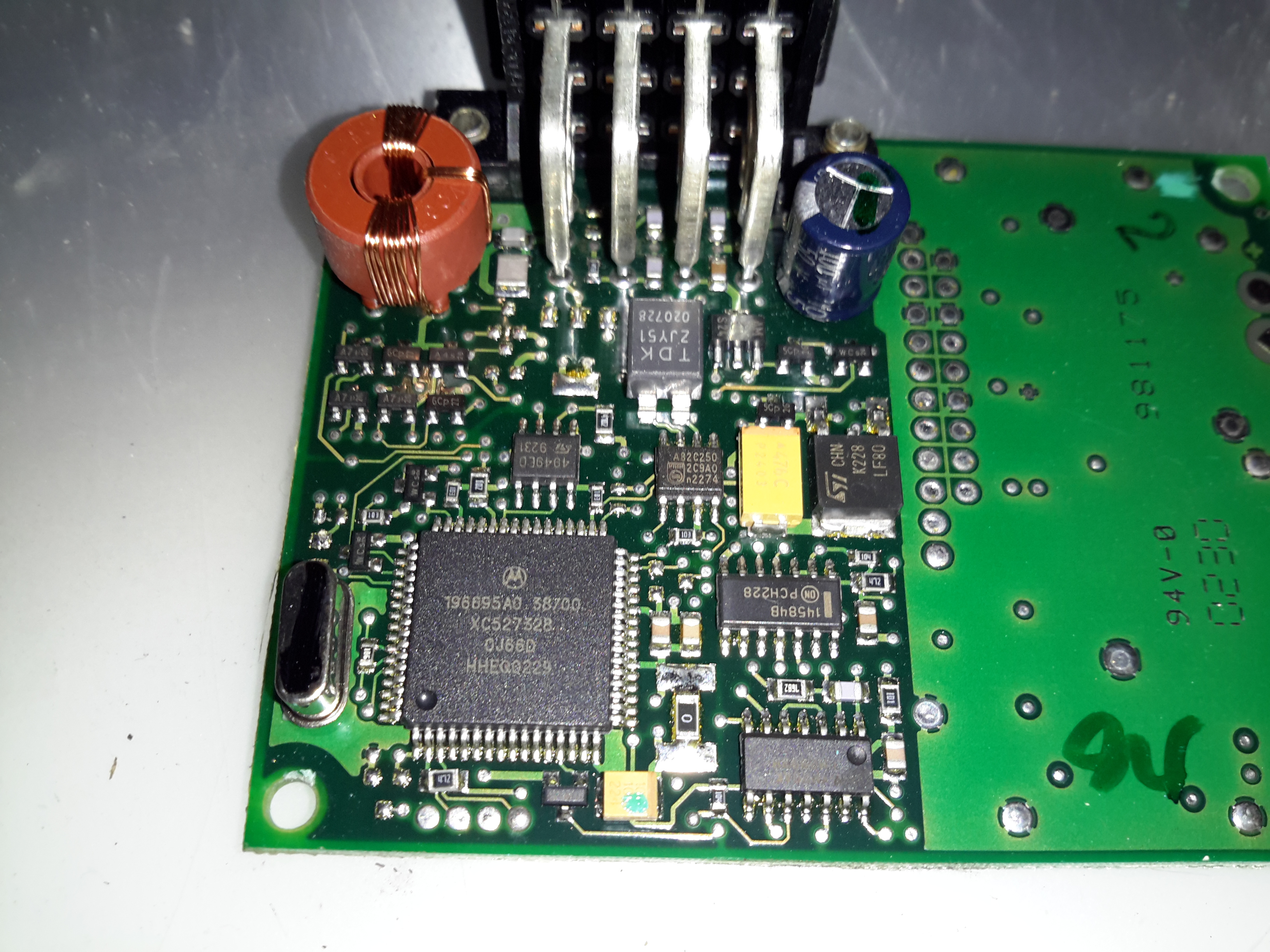
The other day I was given a random pile of car electronic parts from the scrap bin at the local garage, so I decided to do a few teardowns. This first one is a Temic Central Locking / Immobiliser module from a Mercedes van. Judging by the 125kHz stamped on the label, this also has RFID capability.
PCB
The casing just unclips, revealing the PCB. Surprisingly for an automotive module, there is no conformal coating on this (they’re usually heavily coated in protective lacquer to prevent moisture ingress).
Microcontroller
The large IC from Motorola I’m assuming to be a microcontroller, but I didn’t manage to find anything from the markings. There’s not much else in here apart from some glue logic, and what I think is the 125Khz toroidal antenna in the top left corner.
My new DMM I posted about a while back came with PC software & drivers for the RS-232 interface, on a CD. I haven’t used CDs for some time, so I had to dig out my USB drive.
The Tenma website doesn’t list the software for all their models, so to help others I’m posting an archive of all the supplied drivers here. The archive contains software & drivers for the following Tenma models:
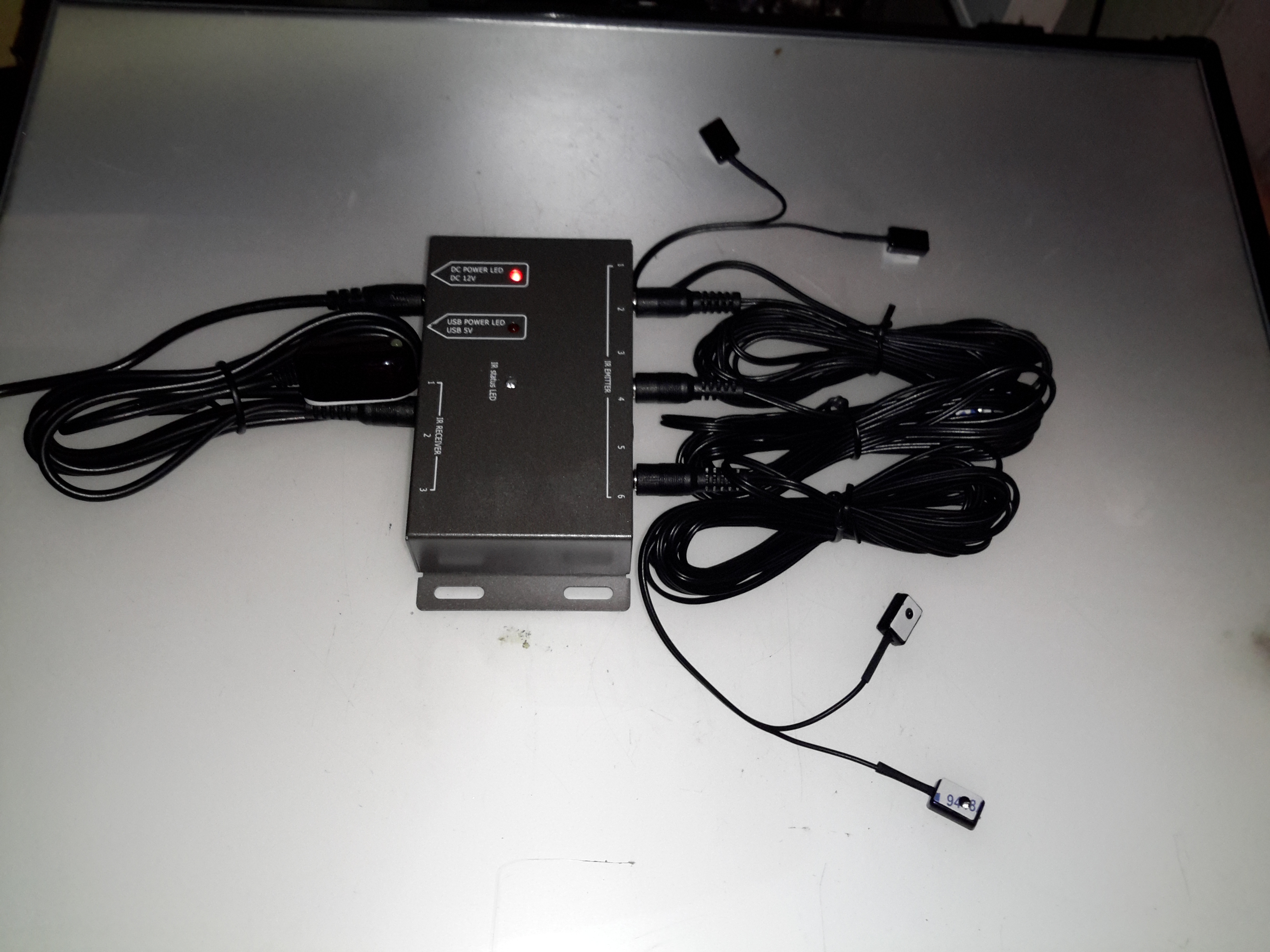
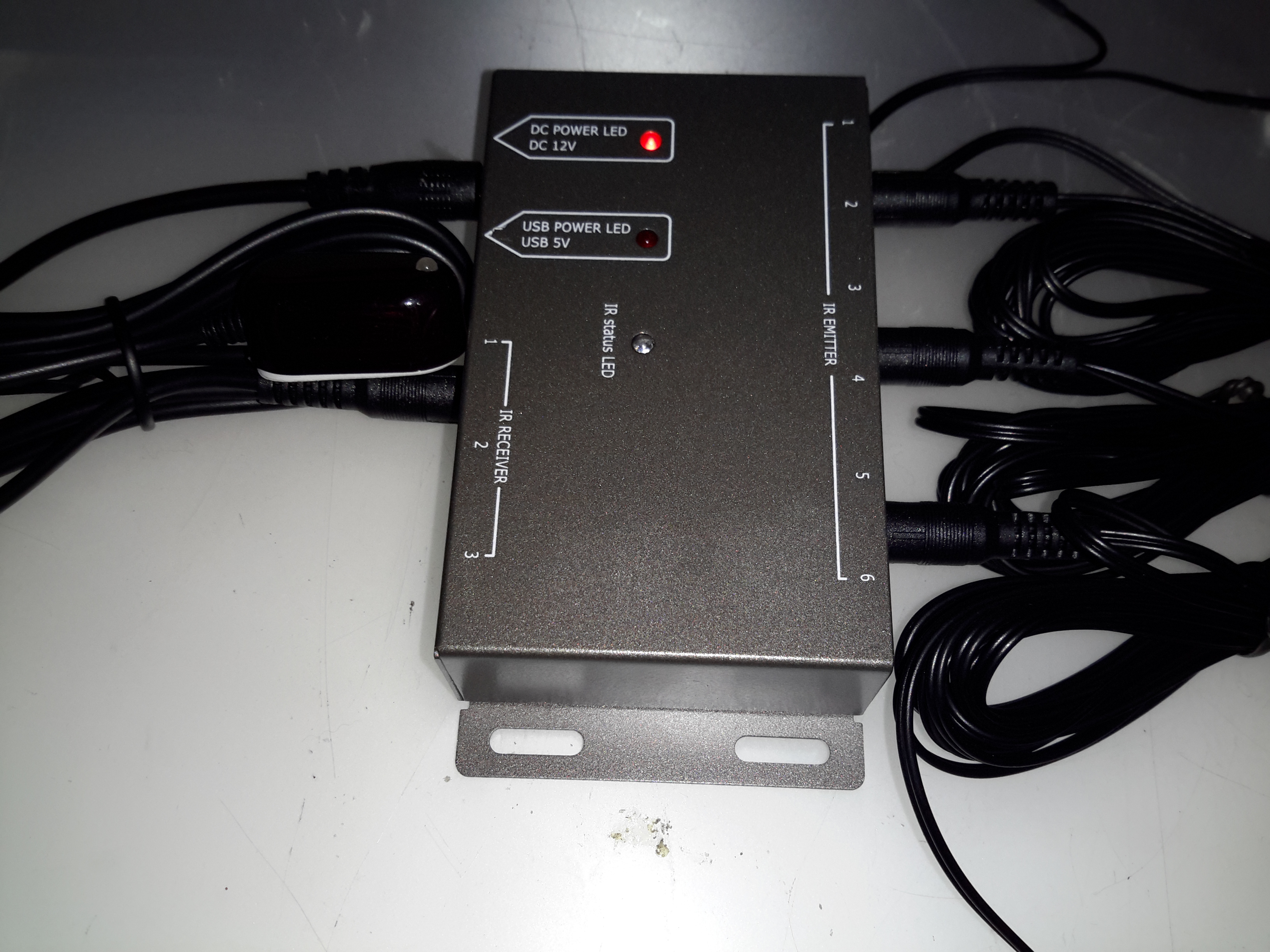
Here’s another random gadget for teardown, this time an IR remote control repeater module. These would be used where you need to operate a DVD player, set top box, etc in another room from the TV that you happen to be watching. An IR receiver sends it’s signal down to the repeater box, which then drives IR LEDs to repeat the signal.
Repeater Module
Not much to day about the exterior of this module, the IR input is on the left, up to 3 receivers can be connected. The outputs are on the right, up to 6 repeater LEDs can be plugged in. Connections are done through standard 3.5mm jacks.
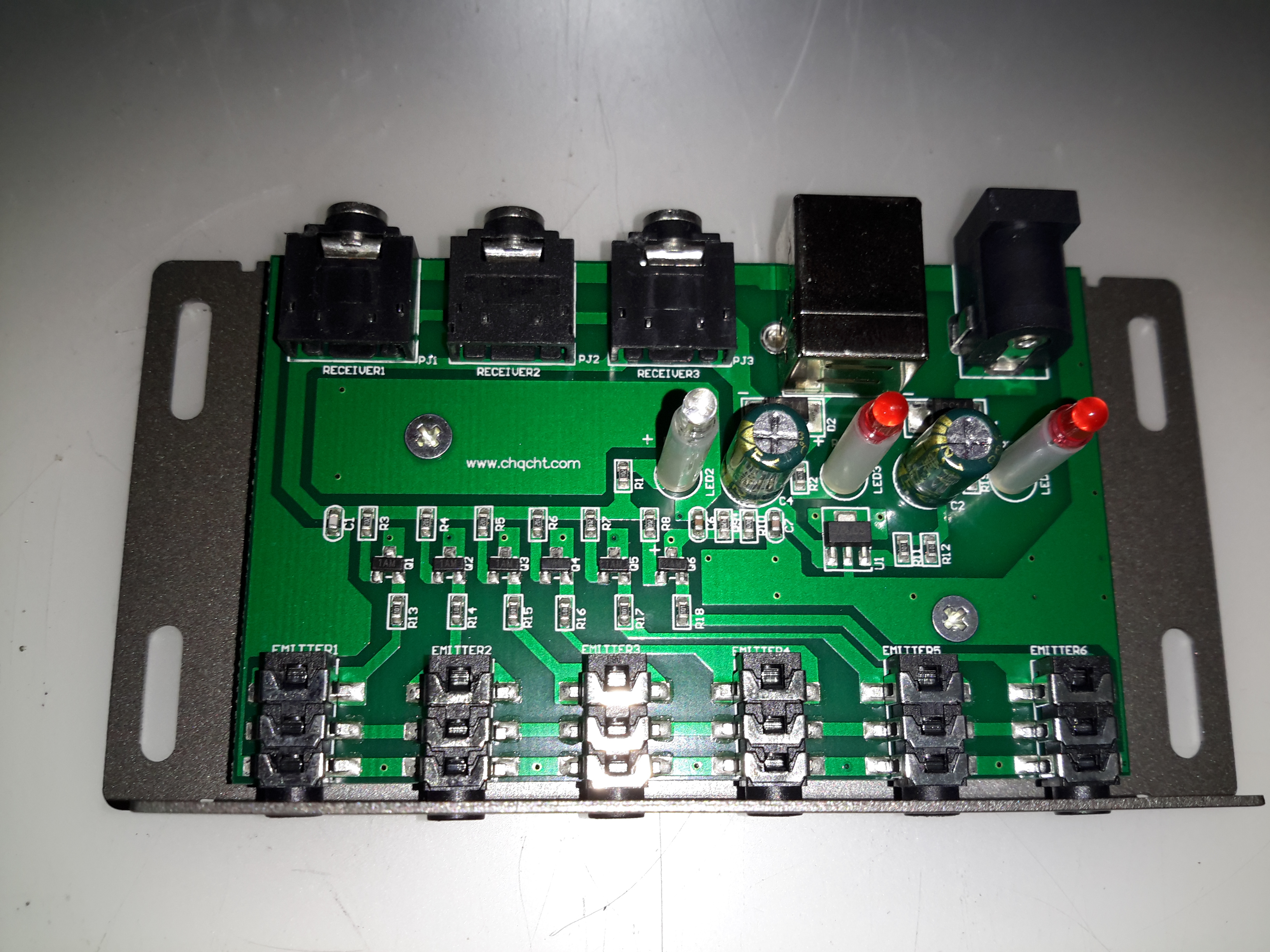
Repeater PCB
Not much inside this one at all, there are 6 transistors which each drive an LED output. This “dumb” configuration keeps things very simple, no signal processing has to be done. Power is either provided by a 12v input, which is fed into a 7805 linear regulator, or direct from USB.
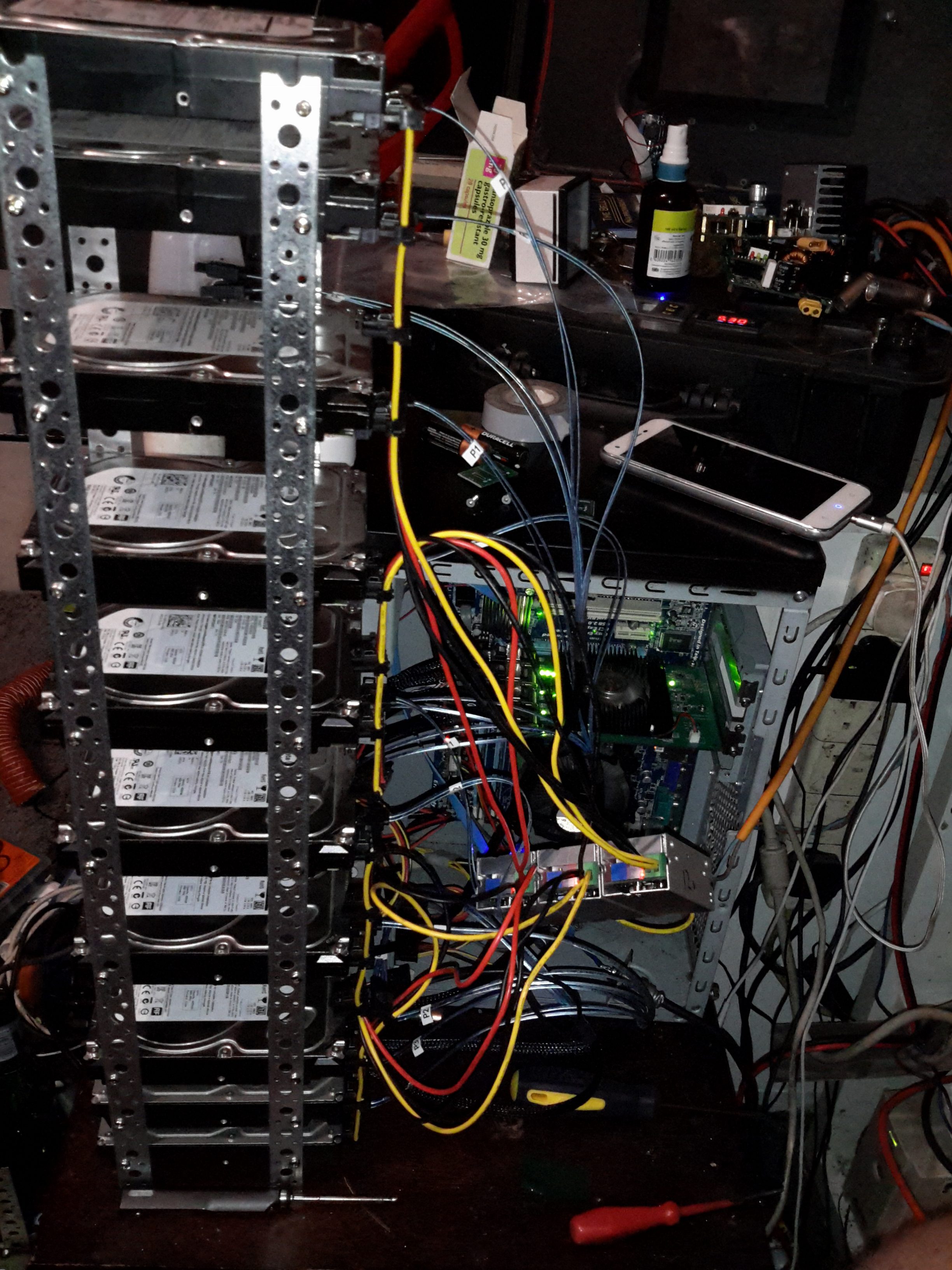
For some time now I’ve been running a large disk array to store all the essential data for my network. The current setup has 10x 4TB disks in a RAID6 array under Linux MD.
Up until now the disks have been running in external Orico 9558U3 USB3 drive bays, through a PCIe x1 USB3 controller. However in this configuration there have been a few issues:
Congestion over the USB3 link. RAID rebuild speeds were severely limited to ~20MB/s in the event of a failure. General data transfer was equally as slow.
Drive dock general reliability. The drive bays are running a USB3 – SATA controller with a port expander, a single drive failure would cause the controller to reset all disks on it’s bus. Instead of losing a single disk in the array, 5 would disappear at the same time.
Cooling. The factory fitted fans in these bays are total crap – and very difficult to get at to change. A fan failure quickly allows the disks to heat up to temperatures that would cause failure.
Upgrade options difficult. These bays are pretty expensive for what they are, and adding more disks to the USB3 bus would likely strangle the bandwidth even further.
Disk failure difficult to locate. The USB3 interface doesn’t pass on the disk serial number to the host OS, so working out which disk has actually failed is difficult.
To remedy these issues, a proper SATA controller solution was required. Proper hardware RAID controllers are incredibly expensive, so they’re out of the question, and since I’m already using Linux MD RAID, I didn’t need a hardware controller anyway.
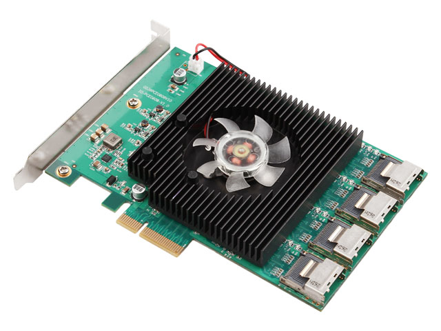
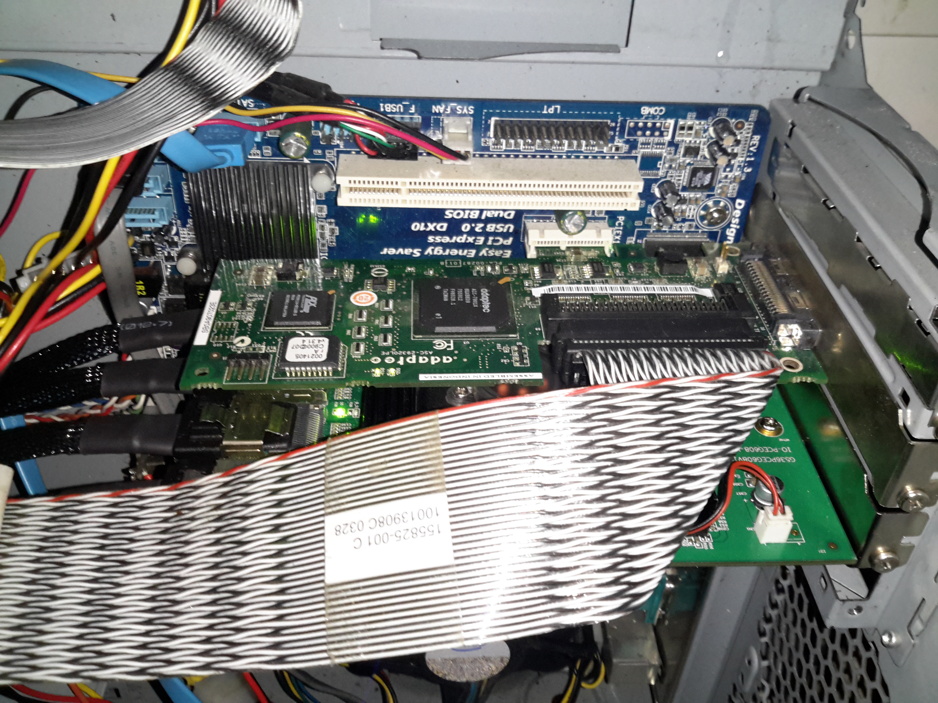
16-Port HBA
A quick search for suitable HBA cards showed me the IOCrest 16-port SATAIII controller, which is pretty low cost at £140. This card breaks out the SATA ports into standard SFF-8086 connectors, with 4 ports on each. Importantly the cables to convert from these server-grade connectors to standard SATA are supplied, as they’re pretty expensive on their own (£25 each).
This card gives me the option to expand the array to 16 disks eventually, although the active array will probably be kept at 14 disks with 2 hot spares, this will give a total capacity of 48TB.
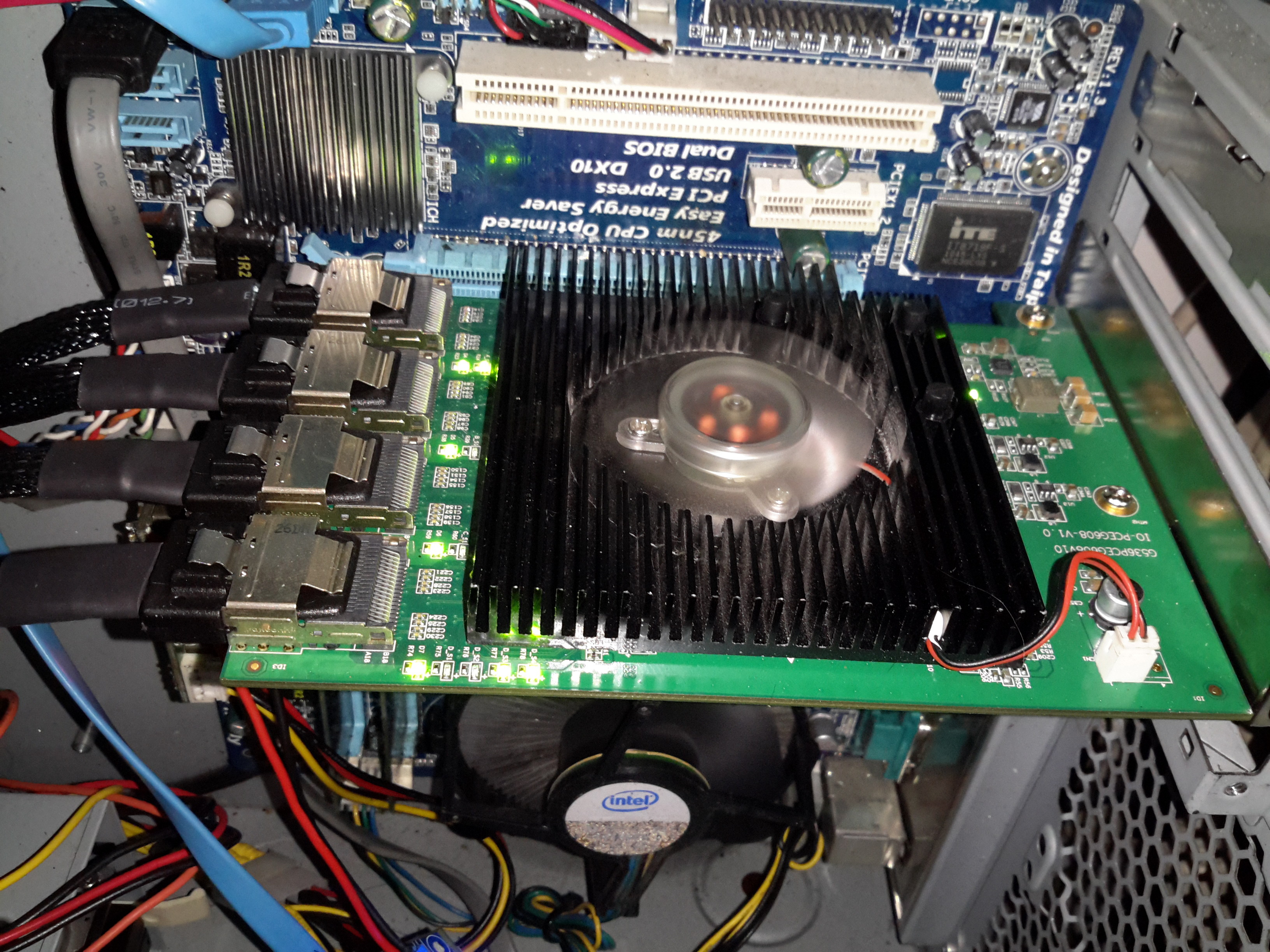
SATA HBA
Here’s the card installed in the host machine, with the array running. One thing I didn’t expect was the card to be crusted with activity LEDs. There appears to be one LED for each pair of disks, plus a couple others which I would expect are activity on the backhaul link to PCIe. (I can’t be certain, as there isn’t any proper documentation anywhere for this card. It certainly didn’t come with any ;)).
I’m not too impressed with the fan that’s on the card – it’s a crap sleeve bearing type, so I’ll be keeping a close eye on this for failure & will replace with a high quality ball-bearing fan when it finally croaks. The heatsink is definitely oversized for the job, with nothing installed above the card barely gets warm, which is definitely a good thing for life expectancy.
Update 10/02/17 – The stock fan is now dead as a doornail after only 4 months of continuous operation. Replaced with a high quality ball-bearing 80mm Delta fan to keep things running cool. As there is no speed sense line on the stock fan, the only way to tell it was failing was by the horrendous screeching noise of the failing bearings.
SCSI Controller
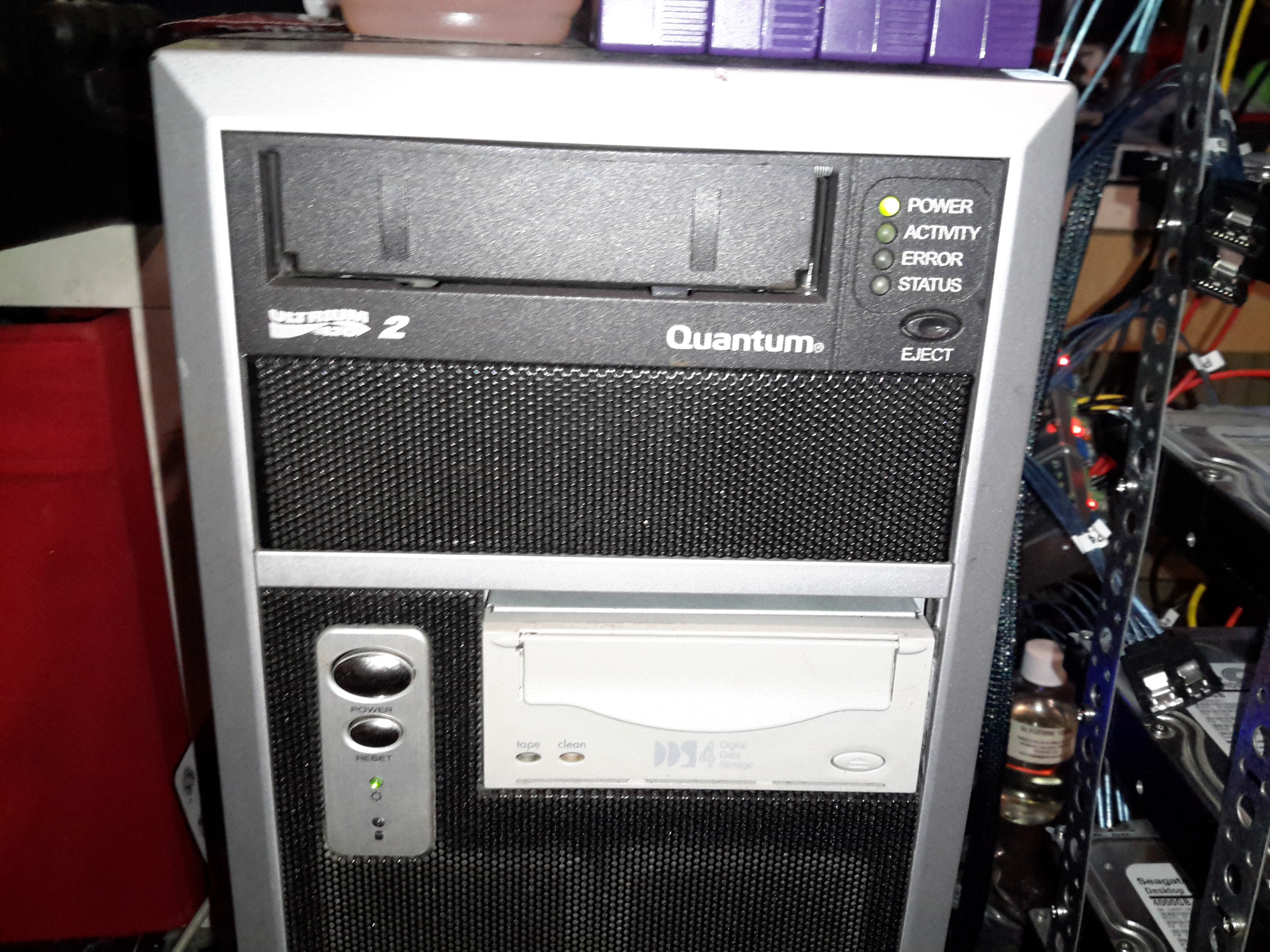
Above is the final HBA installed in the PCIe x1 slot above – a parallel SCSI U320 card that handles the tape backup drives. This card is very close to the cooling fan of the SATA card, and does make it run warmer, but not excessively warm. Unfortunately the card is too long for the other PCIe socket – it fouls on the DIMM slots.
Backup Drives
The tape drives are LTO2 300/600GB for large file backup & DDS4 20/40GB DAT for smaller stuff. These were had cheap on eBay, with a load of tapes. Newer LTO drives aren’t an option due to cost.
The main disk array is currently built as 9 disks in service with a single hot spare, in case of disk failure, this gives a total size after parity of 28TB:
/dev/md0:
        Version : 1.2
  Creation Time : Wed Mar 11 16:01:01 2015
     Raid Level : raid6
     Array Size : 27348211520 (26081.29 GiB 28004.57 GB)
  Used Dev Size : 3906887360 (3725.90 GiB 4000.65 GB)
   Raid Devices : 9
  Total Devices : 10
    Persistence : Superblock is persistent

  Intent Bitmap : Internal

    Update Time : Mon Nov 14 14:28:59 2016
          State : active
 Active Devices : 9
Working Devices : 10
 Failed Devices : 0
  Spare Devices : 1

         Layout : left-symmetric
     Chunk Size : 64K

           Name : Main-PC:0
           UUID : 266632b8:2a8a3dd3:33ce0366:0b35fad9
         Events : 773938

    Number   Major   Minor   RaidDevice State
       0       8       48        0      active sync   /dev/sdd
       1       8       32        1      active sync   /dev/sdc
       9       8       96        2      active sync   /dev/sdg
      10       8      112        3      active sync   /dev/sdh
      11       8       16        4      active sync   /dev/sdb
       5       8      176        5      active sync   /dev/sdl
       6       8      144        6      active sync   /dev/sdj
       7       8      160        7      active sync   /dev/sdk
       8       8      128        8      active sync   /dev/sdi

      12       8        0        -      spare   /dev/sda
The disks used are Seagate ST4000DM000 Desktop HDDs, which at this point have ~15K hours on them, and show no signs of impending failure.
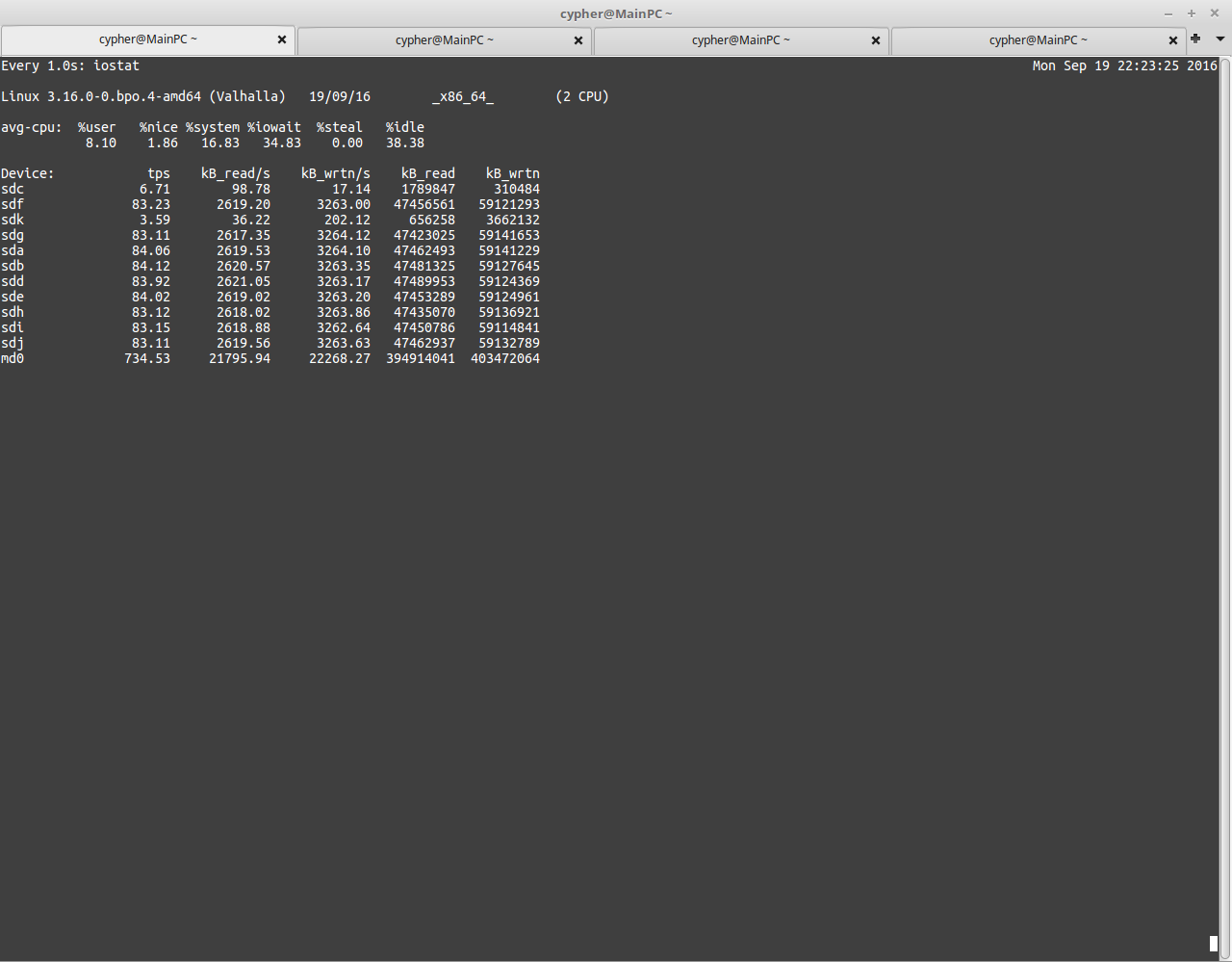
USB3 Speeds
Here’s a screenshot with the disk array fully loaded running over USB3. The aggregate speed on the md0 device is only 21795KB/s. Extremely slow indeed.
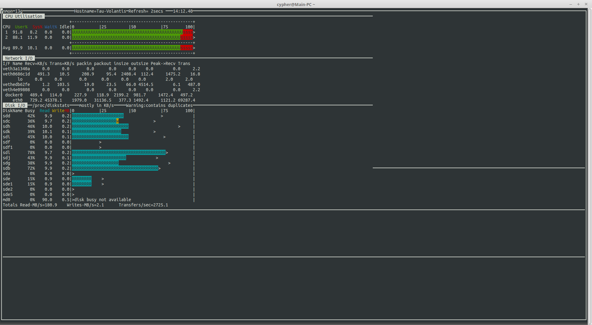
This card is structured similarly to the external USB3 bays – a PCI Express bridge glues 4 Marvell 9215 4-port SATA controllers into a single x8 card. Bus contention may become an issue with all 16 ports used, but as far with 9 active devices, the performance increase is impressive. Adding another disk to the active array would certainly give everything a workout, as rebuilding with an extra disk will hammer both read from the existing disks & will write to the new.
HBA Speeds
With all disks on the new controller, I’m sustaining read speeds of 180MB/s. (Pulling data off over the network). Write speeds are always going to be pretty pathetic with RAID6, as parity calculations have to be done. With Linux MD, this is done by the host CPU, which is currently a Core2Duo E7500 at 2.96GHz, with this setup, I get 40-60MB/s writes to the array with large files.
Disk Array
Since I don’t have a suitable case with built in drive bays, (again, they’re expensive), I’ve had to improvise with some steel strip to hold the disks in a stack. 3 DC-DC converters provides the regulated 12v & 5v for the disks from the main unregulated 12v system supply. Both the host system & the disks run from my central battery-backed 12v system, which acts like a large UPS for this.
The SATA power splitters were custom made, the connectors are Molex 67926-0001 IDC SATA power connectors, with 18AWG cable to provide the power to 4 disks in a string.
IDT Insertion Tool
These require the use of a special tool if you value your sanity, which is a bit on the expensive side at £25+VAT, but doing it without is very difficult. You get a very well made tool for the price though, the handle is anodised aluminium & the tool head itself is a 300 series stainless steel.
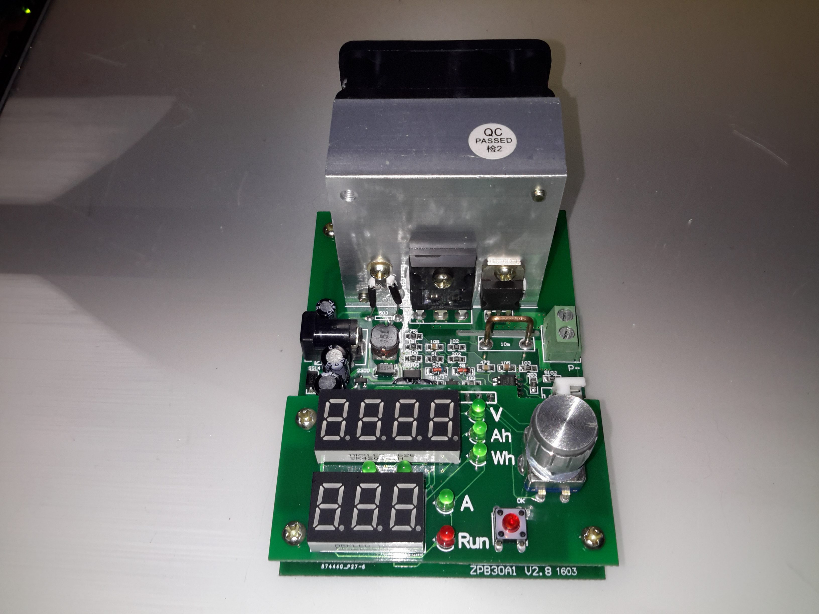
Here’s a useful tool for testing both power supplies & batteries, a dummy load. This unit is rated up to 60W, at voltages from 1v to 25v, current from 200mA to 9.99A.
This device requires a 12v DC power source separate from the load itself, to power the logic circuitry.
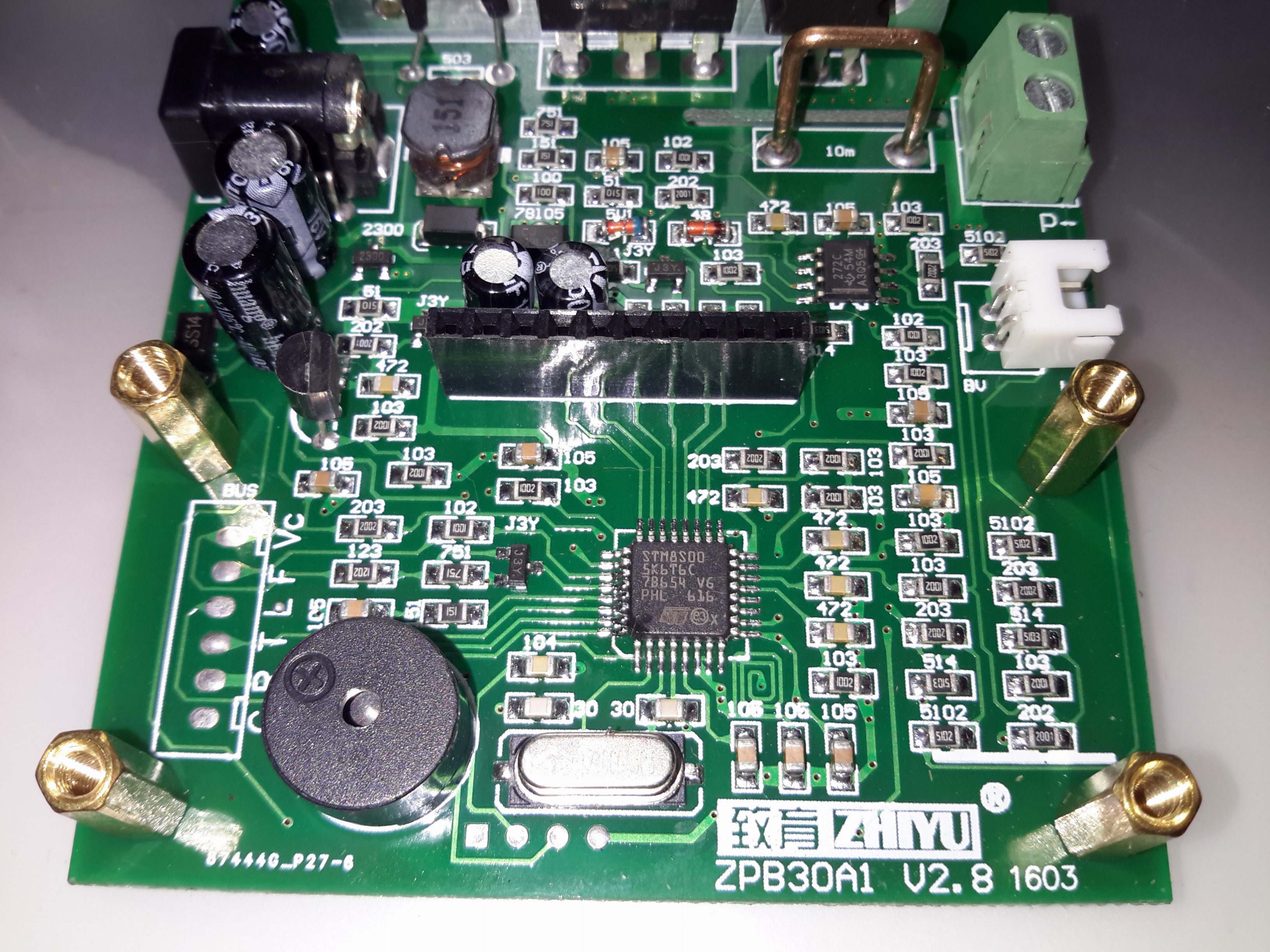
Microcontroller Section
Like many of these modules, the brains of the operation is an STM8 microcontroller. There’s a header to the left with some communication pins, the T pin transmits the voltage when the unit is operating, along with the status via RS232 115200 8N1. This serial signal is only present in DC load mode, the pin is pulled low in battery test mode. The 4 pins underneath the clock crystal are the programming pins for the STM8.
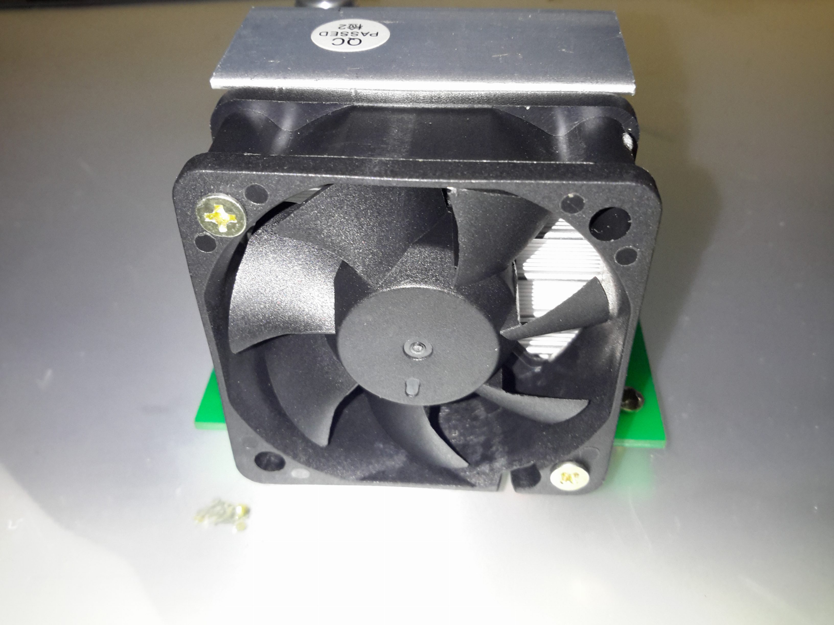
Serial CommsCooling Fan
The main heatsink is fan cooled, the speed is PWM controlled via the microcontroller depending on the temperature.
Main MOSFET
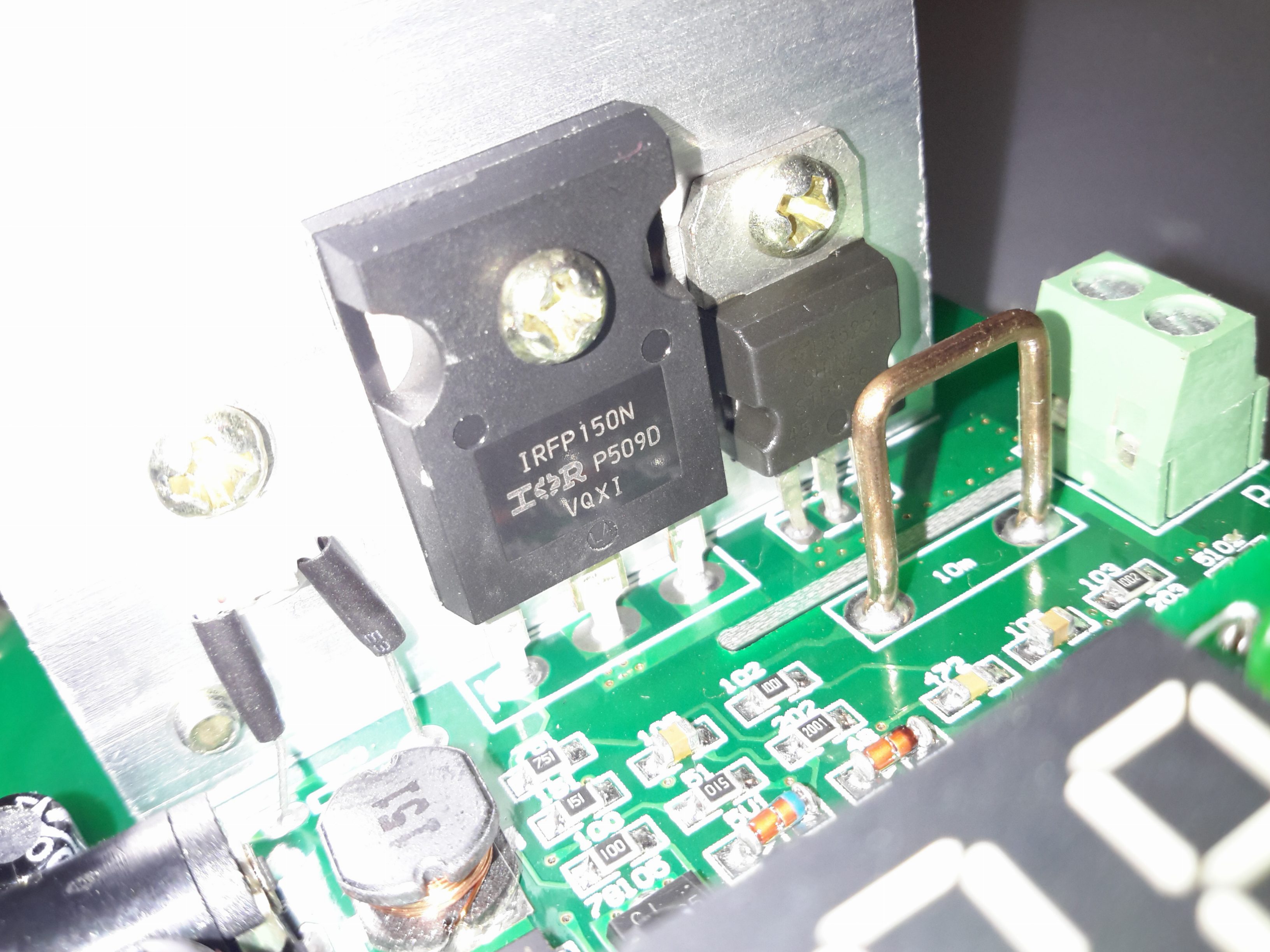
The main load MOSFET is an IRFP150N from Infineon. This device is rated at 100v 42A, with a max power dissipation of 160W. On the right is a dual diode for reverse polarity protection, this is in series with the MOSFET. On the left is the thermistor for controlling fan speed.
Load Terminals
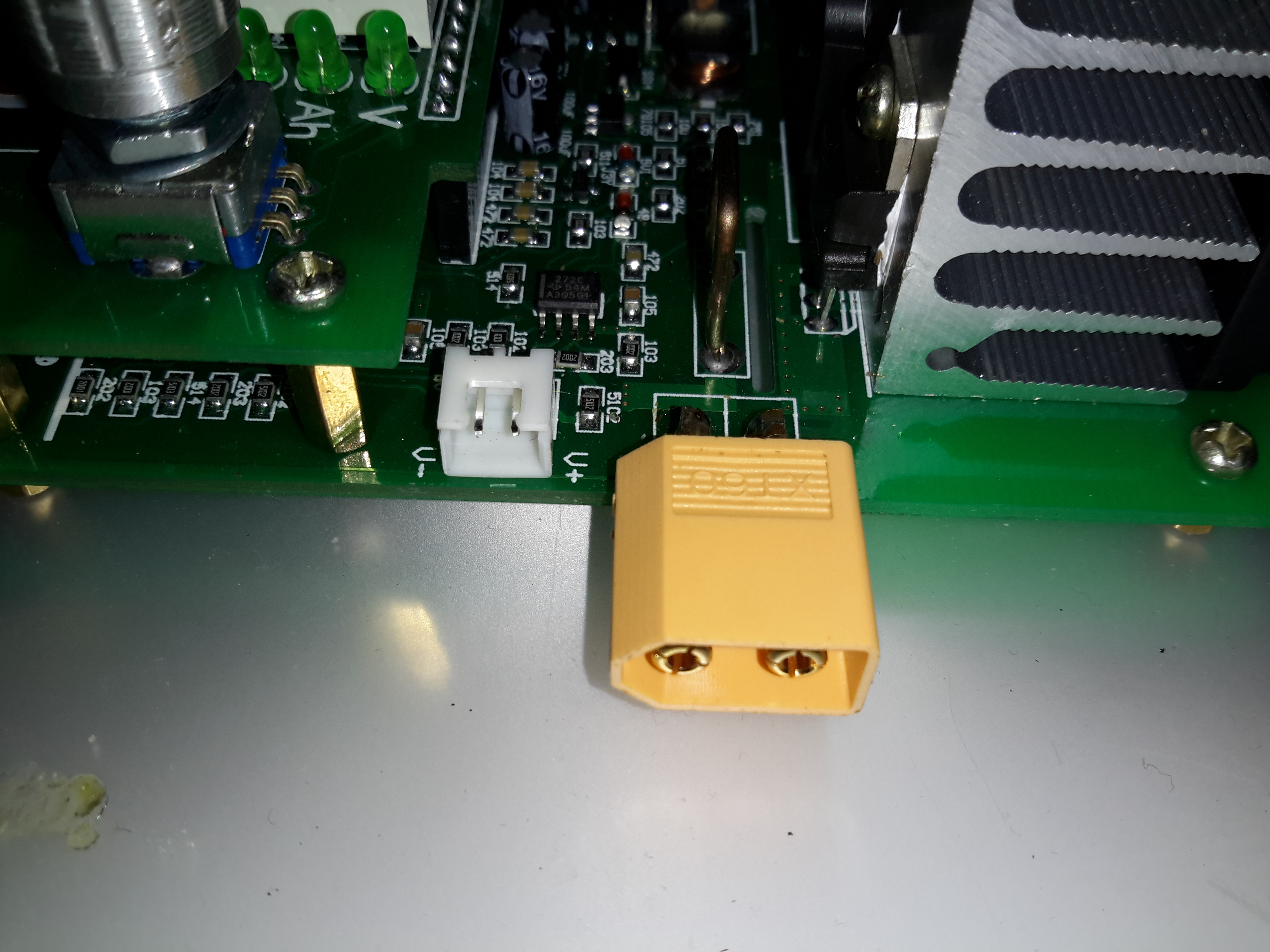
The load is usually connected via a rising clamp terminal block. I’ve replaced it with a XT60 connector in this case as all my battery holders are fitted with these. This also removes the contact resistance of more connections for an adaptor cable. The small JST XH2 connector on the left is for remote voltage sensing. This is used for 4-wire measurements.
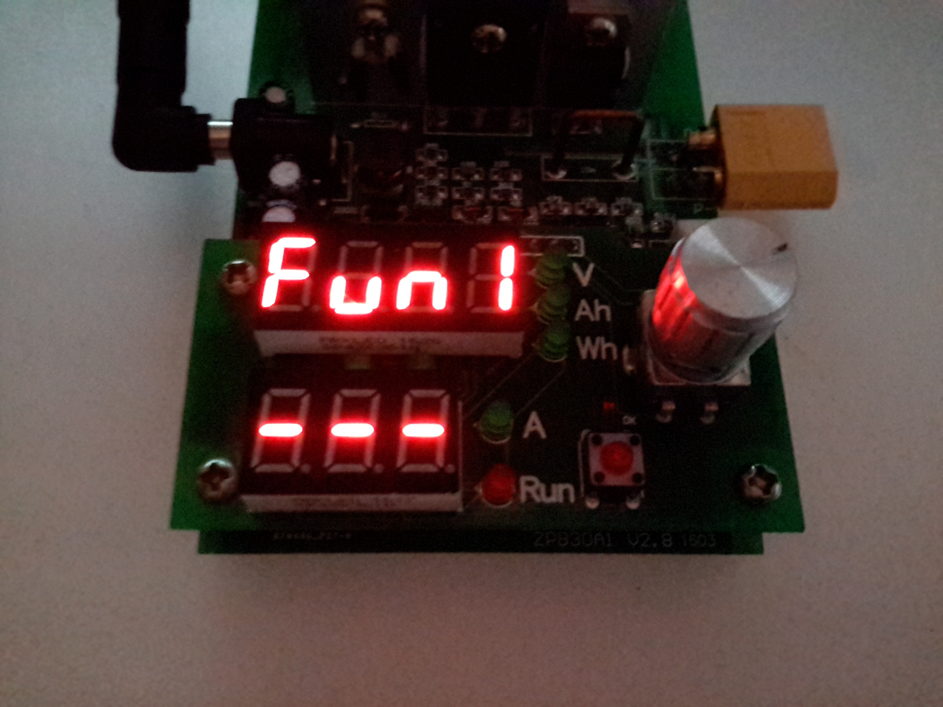
Function 1 – DC Load
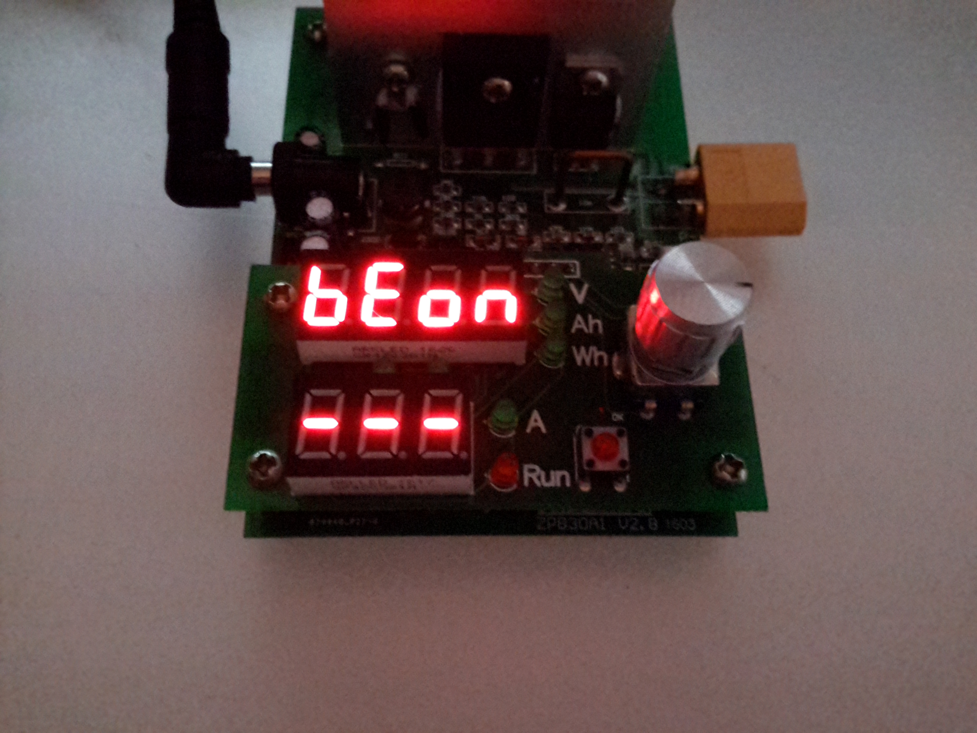
Powering the device up while holding the RUN button gets you into the menu to select the operating modes. Function 1 is simple DC load.
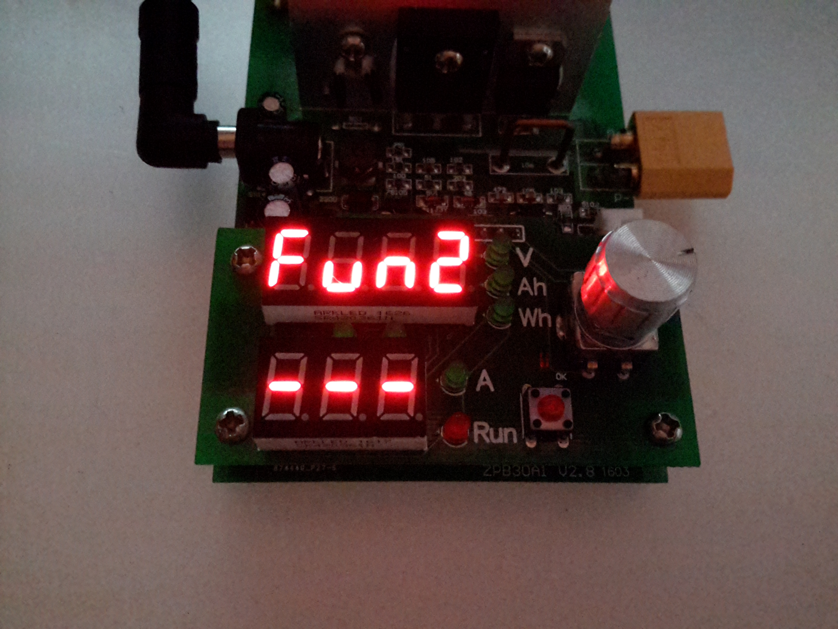
Function 2 – Battery Capacity Mode
The rotary encoder is used to select the option. Function 2 is battery capacity test mode.
Beeper Mode
After the mode is selected, an option appears to either turn the beeper on or off.
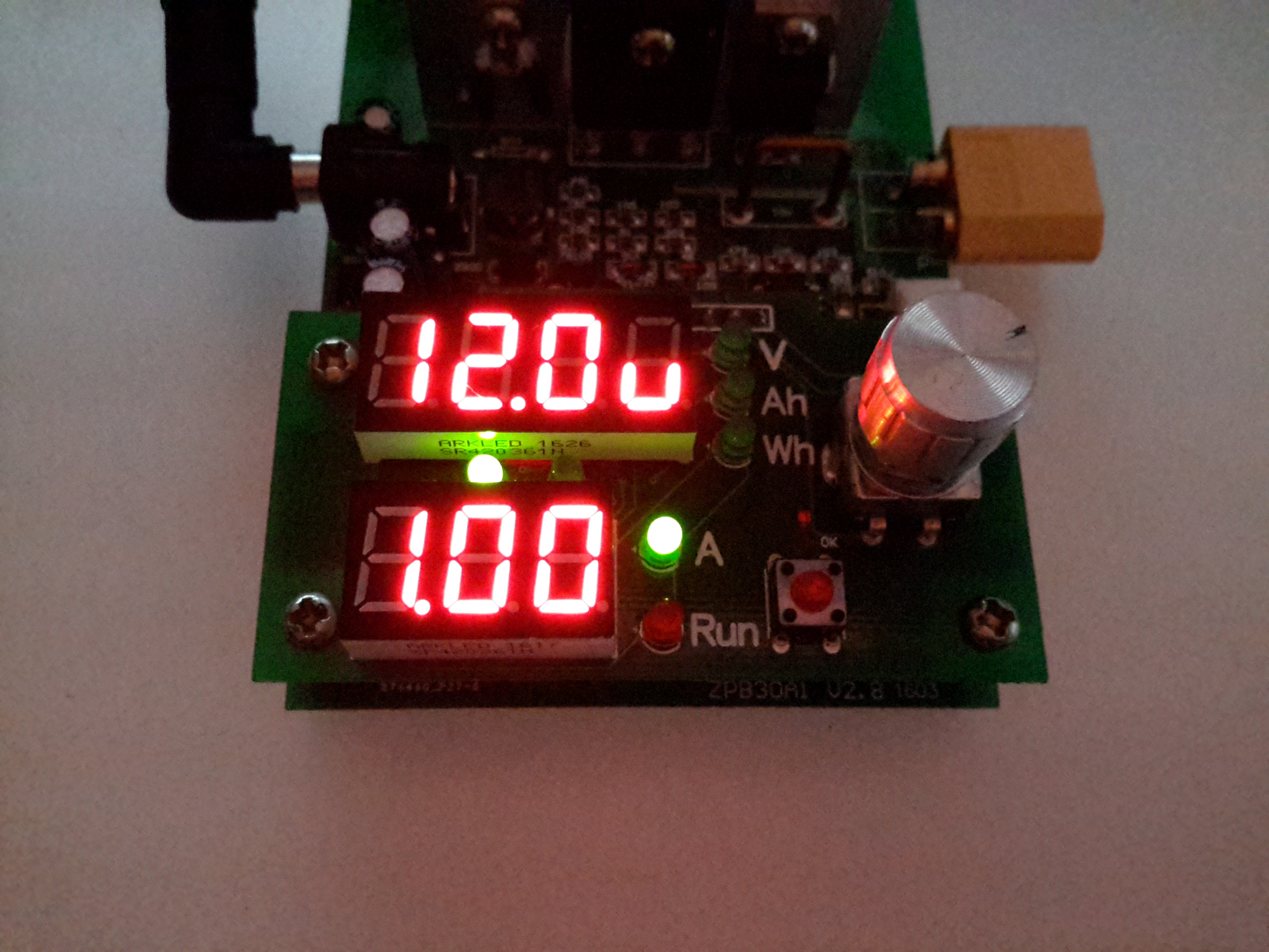
Amps Set
When in standby mode, the threshold voltage & the load current can be set. Here the Amps LED is lit, so the load current can be set. The pair of LEDs between the displays shows which digit will be changed. Pressing the encoder button cycles through the options.
Volts Set
With the Volts LED lit, the threshold voltage can be changed.
When in DC load mode (Fun1), the device will place a fixed load onto the power source until it’s manually stopped. The voltage setting in this mode is a low-voltage alarm. The current can be changed while the load is running.
When in battery discharge test mode (Fun2), the voltage set is the cutoff voltage – discharge will stop when this is reached. Like the DC load mode, the current can be changed when the load is running. After the battery has completed discharging, the capacity in Ah & Wh will be displayed on the top 7-segment. These results can be selected between with the encoder.
Below are tables with all the options for the unit, along with the error codes I’ve been able to decipher from the Chinese info available in various places online. (If anyone knows better, do let me know!).
Option
Function
Fun1
Basic DC Load
Fun 2
Battery Capacity Test
BeOn
Beeper On
BeOf
Beeper Off
Error Code
Meaning
Err1
Input Overvoltage
Err2
Low Battery Voltage / No Battery Present / Reverse Polarity
Err3
Battery ESR Too High / Cannot sustain selected discharge current
Err4
General Failure
Err6
Power Supply Voltage Too Low / Too High. Minimum 12v 0.5A.
I was recently given a pretty nice LED backlit 1080p LG monitor, with the instruction that it wouldn’t power on correctly. The monitor would power on as far as the standby light, but when fully powered on, would flash the backlight momentarily then shut down. A power supply issue was immediately suspected.
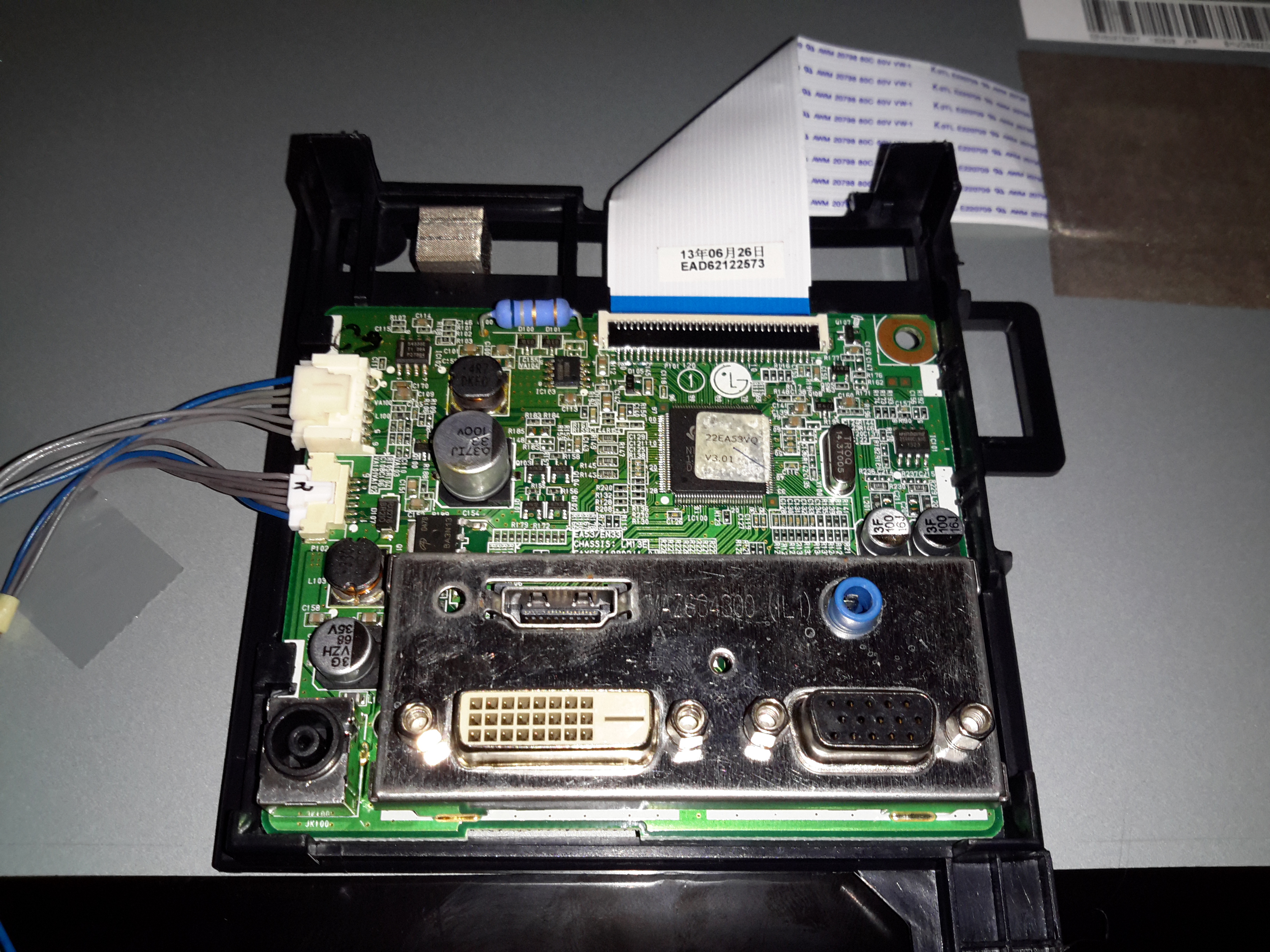
LCD Logic Board
I popped the covers off the monitor itself first, thinking that it was an electrolytic gone bad in the backlight DC-DC converter. Not to mention the fact that cracking into a wall-wart type of PSU is only occasionally possible without the use of anger & large hammers. (Cracking the glue with the handle of a screwdriver doesn’t work so well when the factory went a bit nuts with the glue/ultrasonic welder). As can be seen in the photo, there’s not much inside these monitors, the logic is a single-chip solution, the rest of the PCB is dedicated to supplying the power rails for the various circuits. On the left is the power input & the DC-DC converter for the backlight, along with the DC-DC converter supplying the logic circuits. None of the capacitors here are damaged, everything looks good.
I then measured the output of the PSU, which under no load was the correct 19v DC. However applying any load caused the output voltage to drop like a proverbial brick. Applying a full load of 1.3A saw the output voltage drop so severely that the PSU tripped on it’s UVLO.
200mA Load
At 200mA of load the factory PSU is already dropping to 18v, with a 5.3kHz switching frequency appearing.
500mA Load
At higher load the frequency increases to 11.5kHz & the output voltage has dropped to 11.86v!
750mA Load
750mA was as high as I could make the supply go without it tripping itself out – the UVLO circuit trips at 9v. 12.6kHz is now riding on the severely low DC at this point.
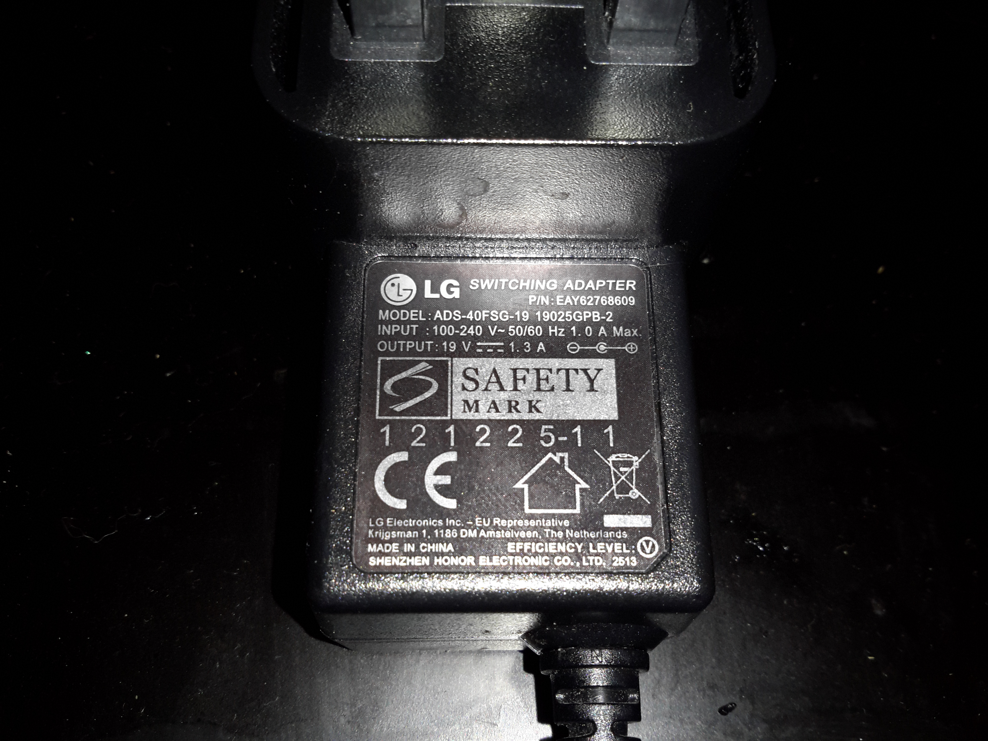
PSU Ratings
The power supply is supposed to be rated at 1.3A at 19v, however with this fault it’s getting nowhere near that. The LG brand is on this PSU but it’s contracted out to Shenzen Honor Electric Co. Ltd.
Output Electrolytic
Here’s the problem with this PSU. The output electrolytic has ballooned. I don’t have an ESR tester, but this cap has gone way past it’s sell-by date. It’s position right next to the heatsink with the output rectifier diodes has probably cooked it. The PSU isn’t that badly built for a Chinese one – there’s plenty of creepage distance on the PCB & even a couple of isolation slots.
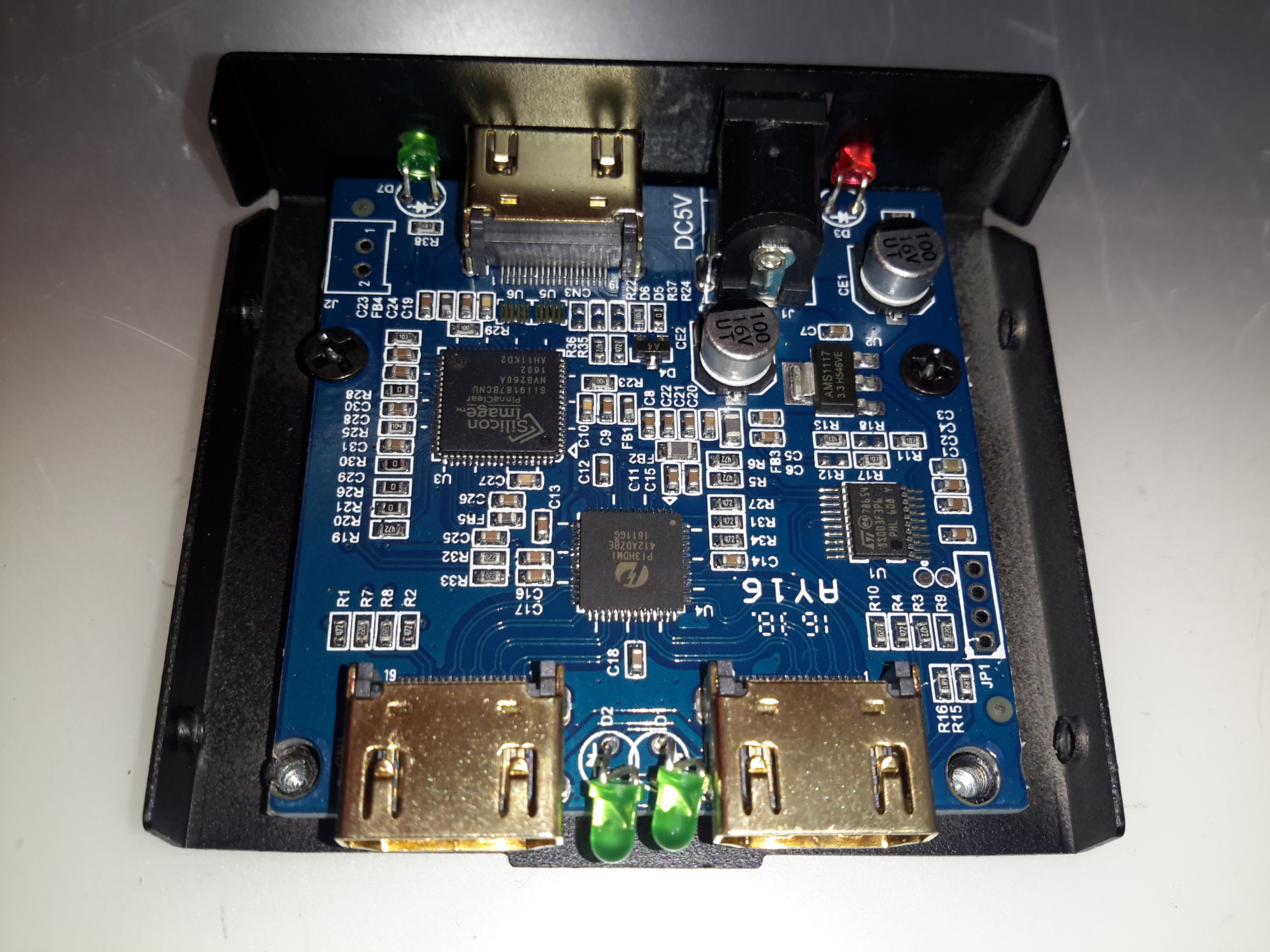
Time for another random teardown, a signal splitter for HDMI. These units are available very cheap these days on eBay. This one splits the incoming signal into two to drive more than one display from the same signal source.
Main PCB
The stamped alloy casing comes apart easily with the removal of a few screws. The PCB inside is rather densely packed with components.
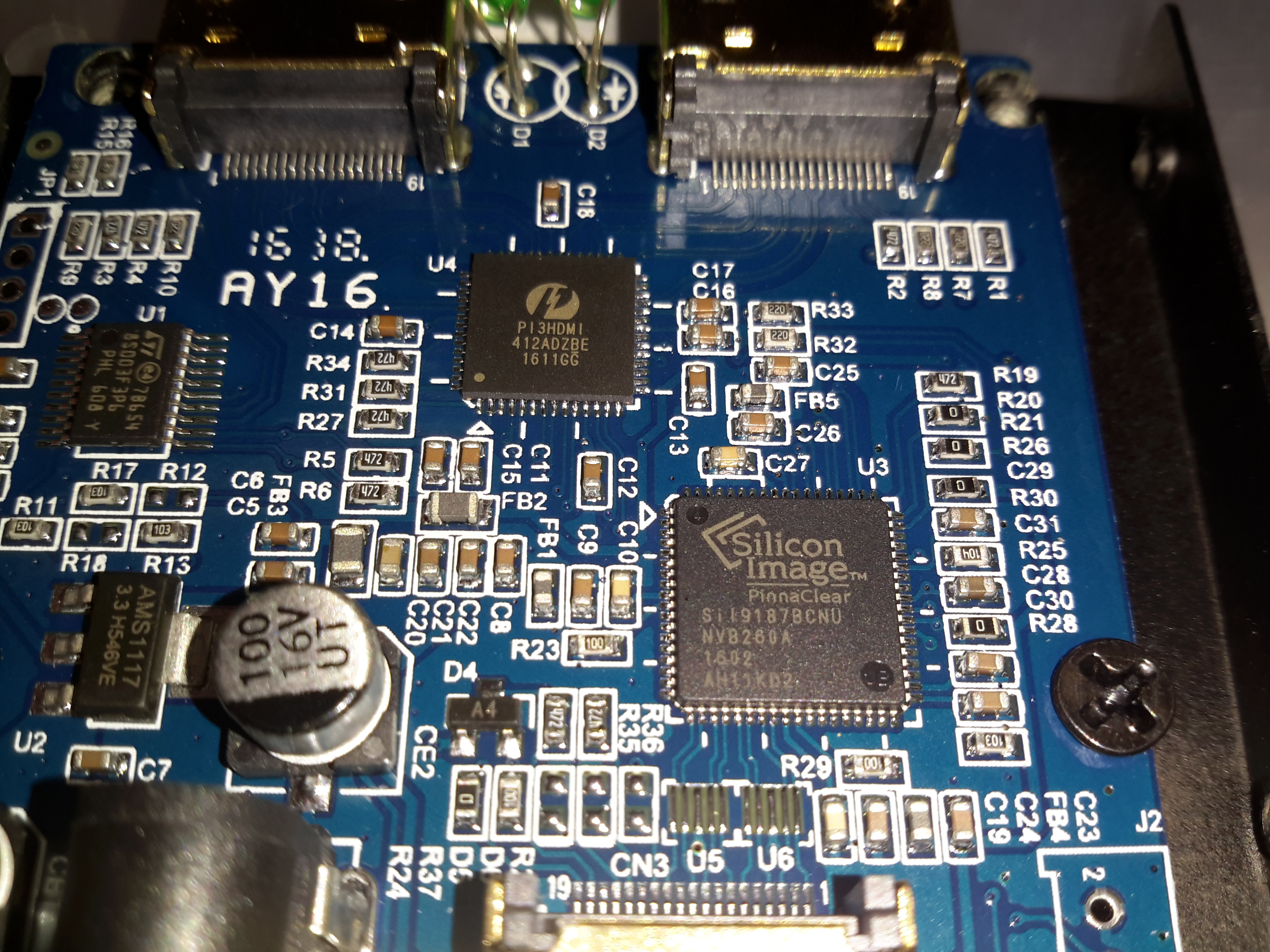
Chipset
The main IC on the incoming signal is a Silicon Image Sil9187B HDMI Port Processor, with a single input & 4 outputs. In this case the chip is used as a repeater to amplify the incoming signal. the signal path then gets fed into a Pericom PI3HDMI412 HDMI Demux, which then splits the signal into two for the output ports.
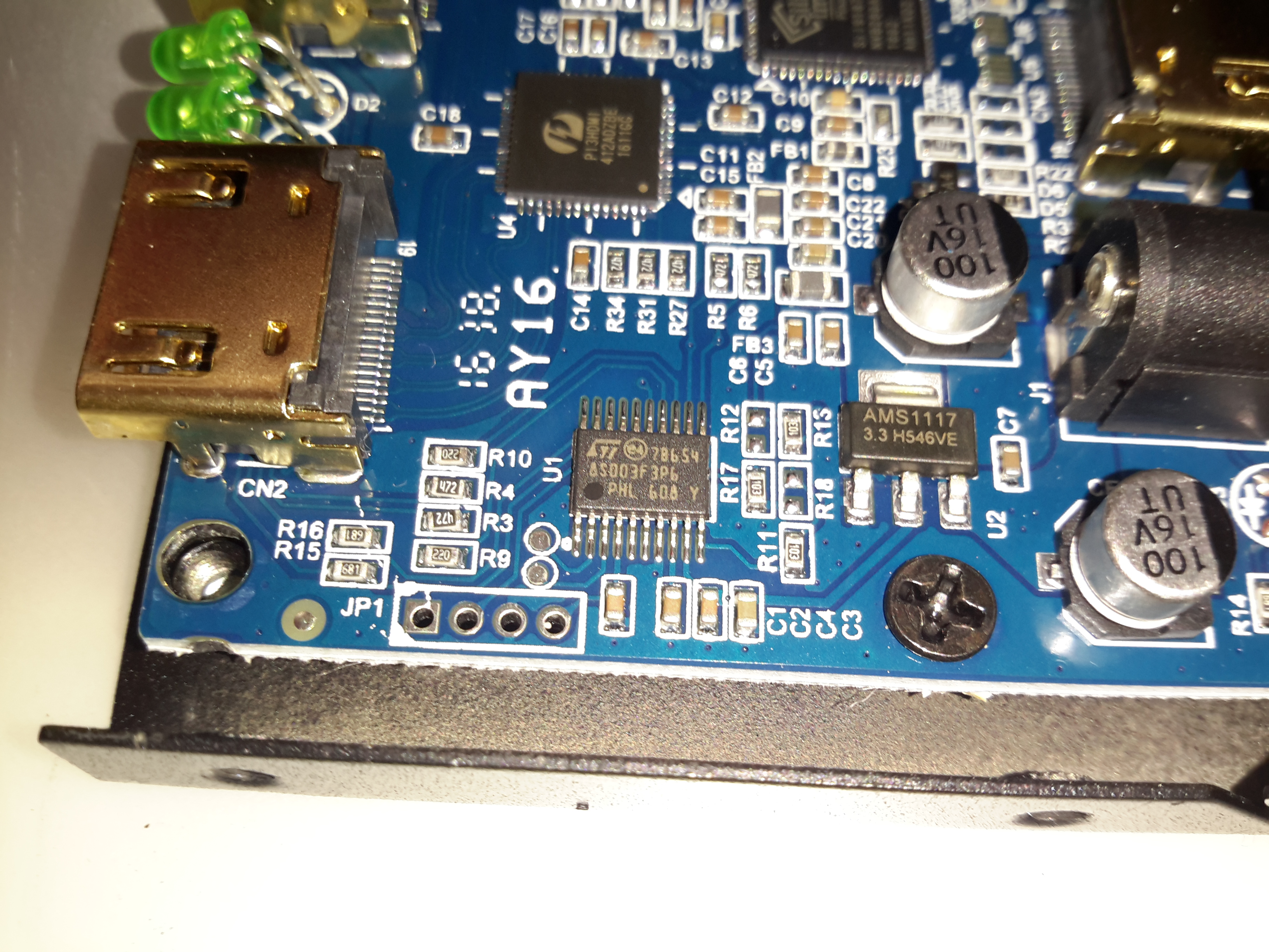
Microcontroller
The main pair of ICs processing the video signals are controlled over I²C, with this STM32 microcontroller. The 4 pads to the lower left are for the STLink programmer. The main 3.3v power rail is provided by the LM1117 linear regulator on the right.
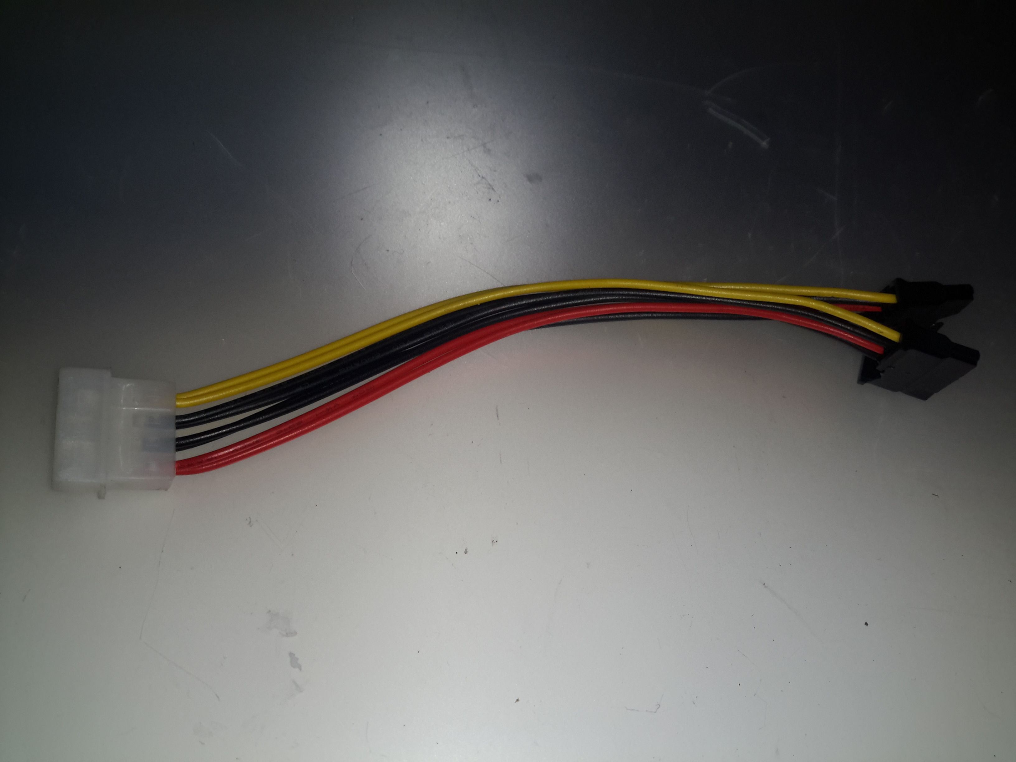
To do some upgrades to my NAS, I needed some SATA power adaptors, to split the PSU out to the planned 16 disk drives. eBay has these for very little money, however there’s a good reason for them being cheap.
Wire Marking
The marking on the wire tells me it’s 18AWG, which should be good for 9.5A at an absolute maximum. However these adaptors are extremely light.
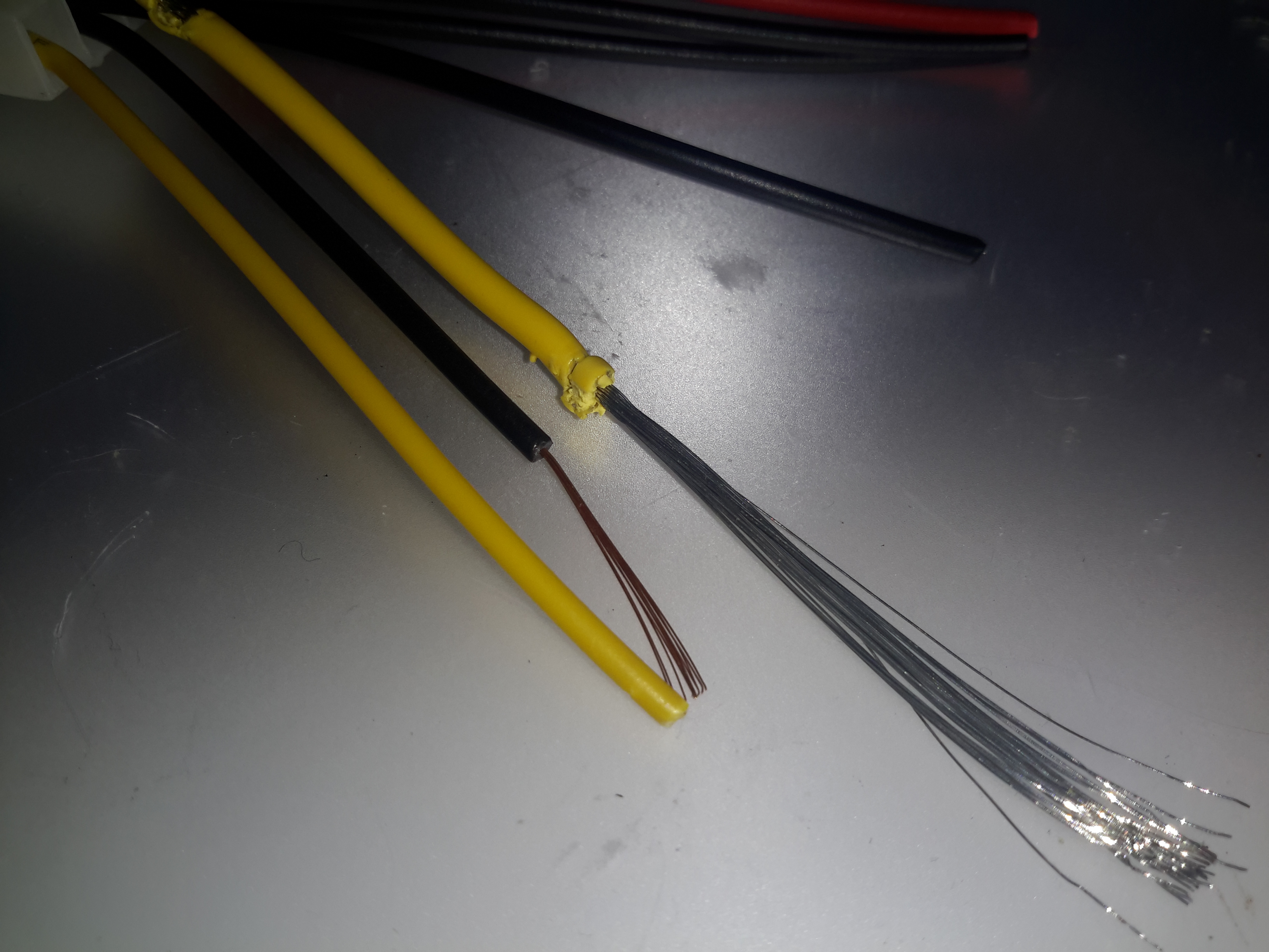
Wire Comparison
Here’s the cheapo eBay wire compared to proper 18AWG wire. The cores in the eBay adaptor are tiny, I’d guess about 24AWG, only good for about 3A. As disk drives pull about 2A from the +12v rail on startup to spin the platters up to speed, this thin wire is going to cause quite the volt drop & possibly prevent the disk from operating correctly.
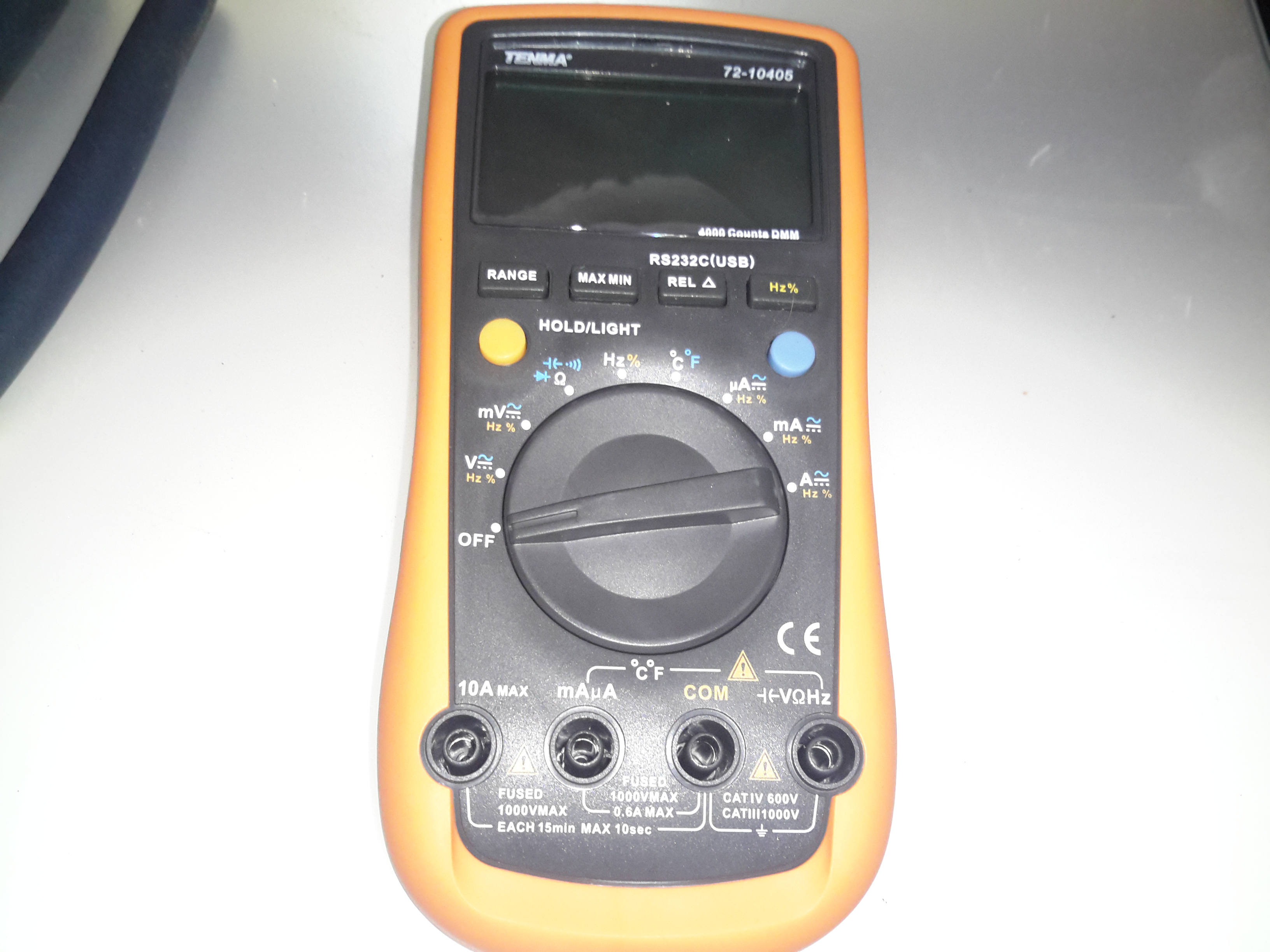
Well it’s time for a new DMM. After the last pair of eBay El-Cheapo Chinese meters just didn’t last very well, I decided a proper meter was required. This one is a Tenma 72-10405, stocked by Farnell for under £60. Not quite as many festures as the cheapo Chinese meters, but I expect this one to be a bit more reliable.
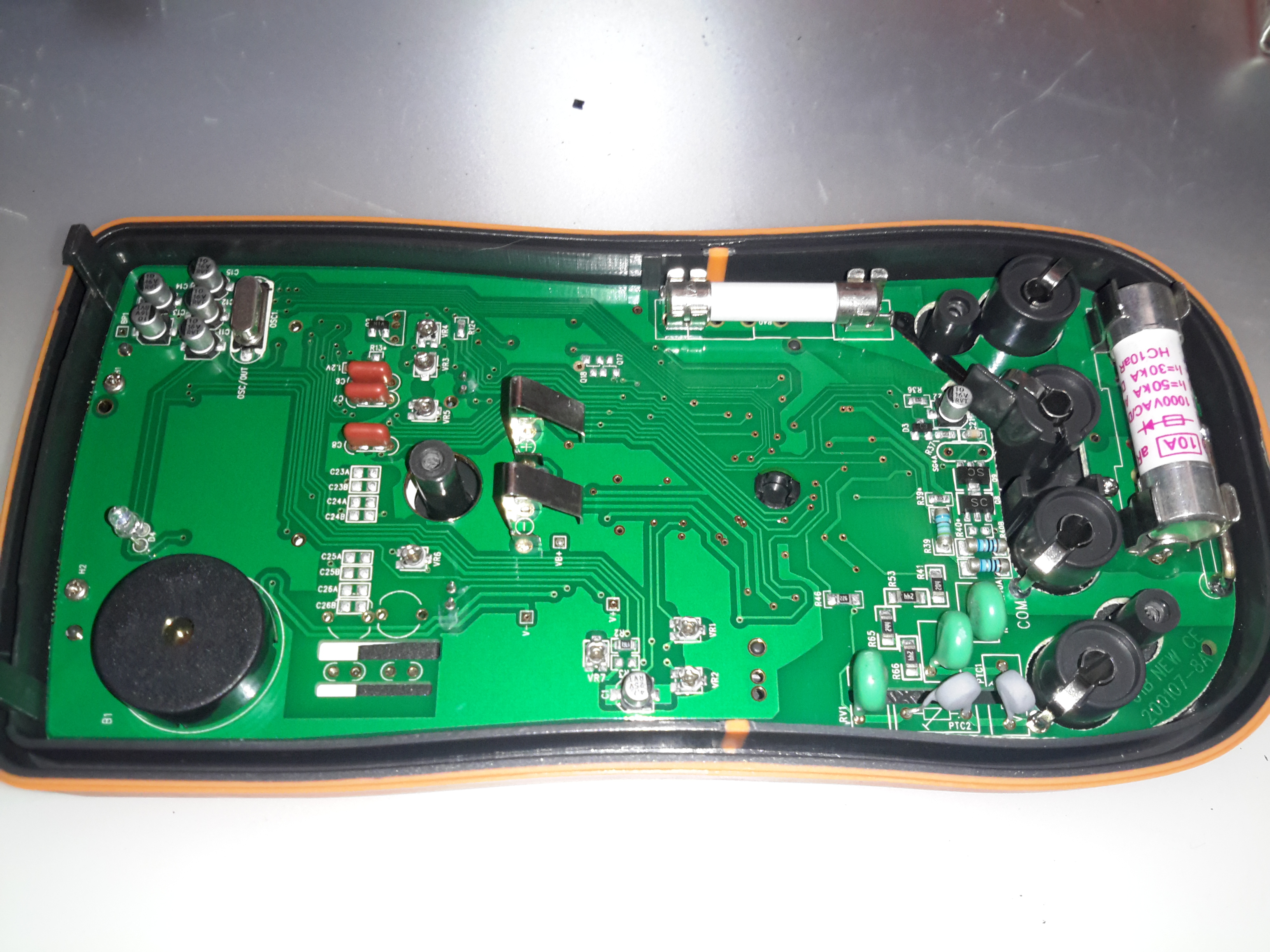
PCB Rear
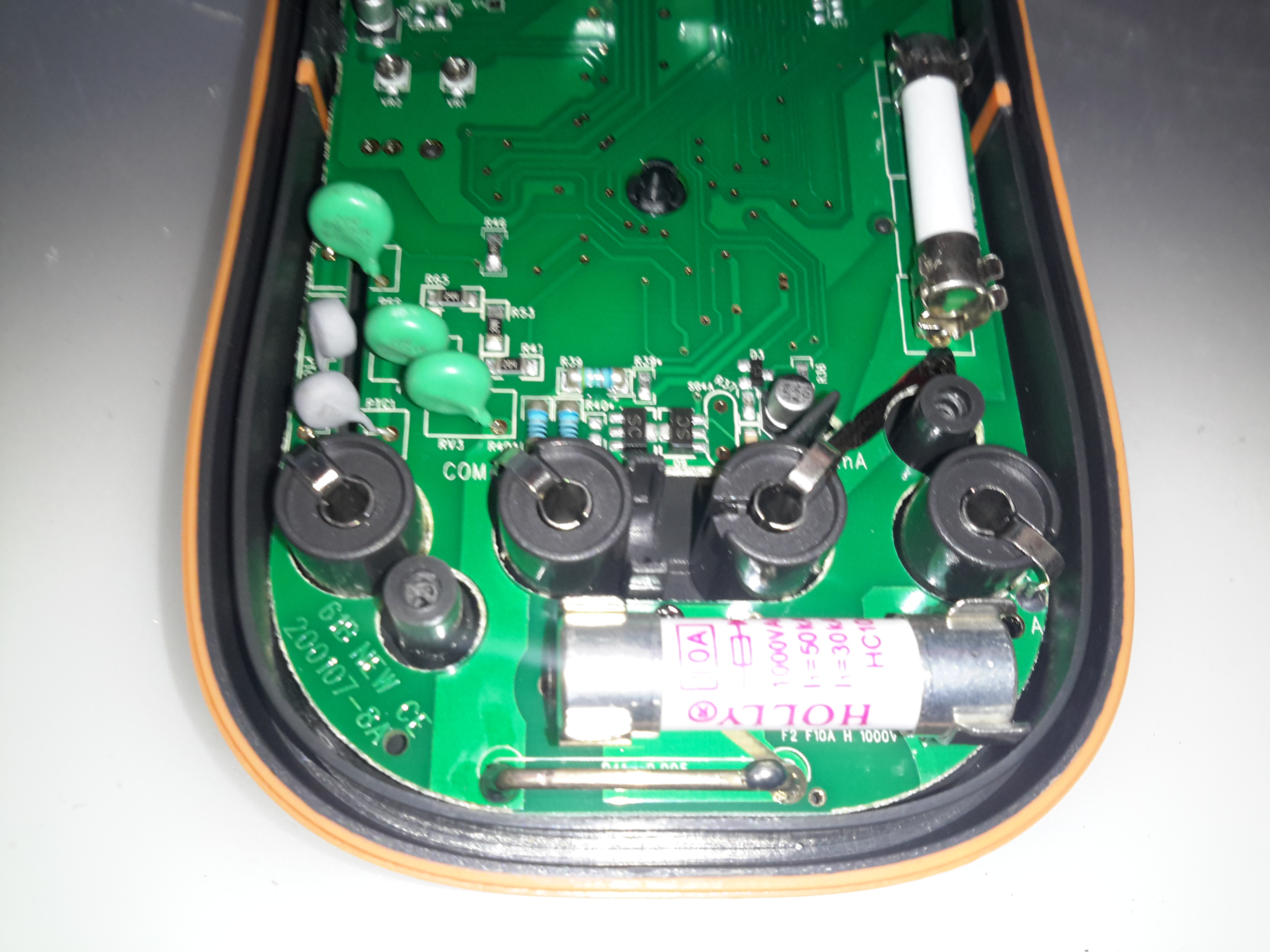
Since I can’t have anything without seeing how it’s put together, here’s the inside of the DMM. (Fuse access is only possible by taking the back cover off as well. The 9v PP3 battery has a seperate cover).
PCB Rear Bottom
He’s the input section of the meter, with the 10A HRC fuse & current shunt for the high-amps range. The other fuse above is for the mA/µA ranges. The back cover has a wide lip around the edge, that slots into a recess in the front cover, presumably for blast protection if the meter should meet a sticky end. The HRC fuses are a definite improvement over the cheap DMMs, they only have 15mm glass fuses, and no blast protection built into the casing.
There are some MOVs for input protection on the volts/ohms jack, the jacks themselves are nothing more than stampings though.
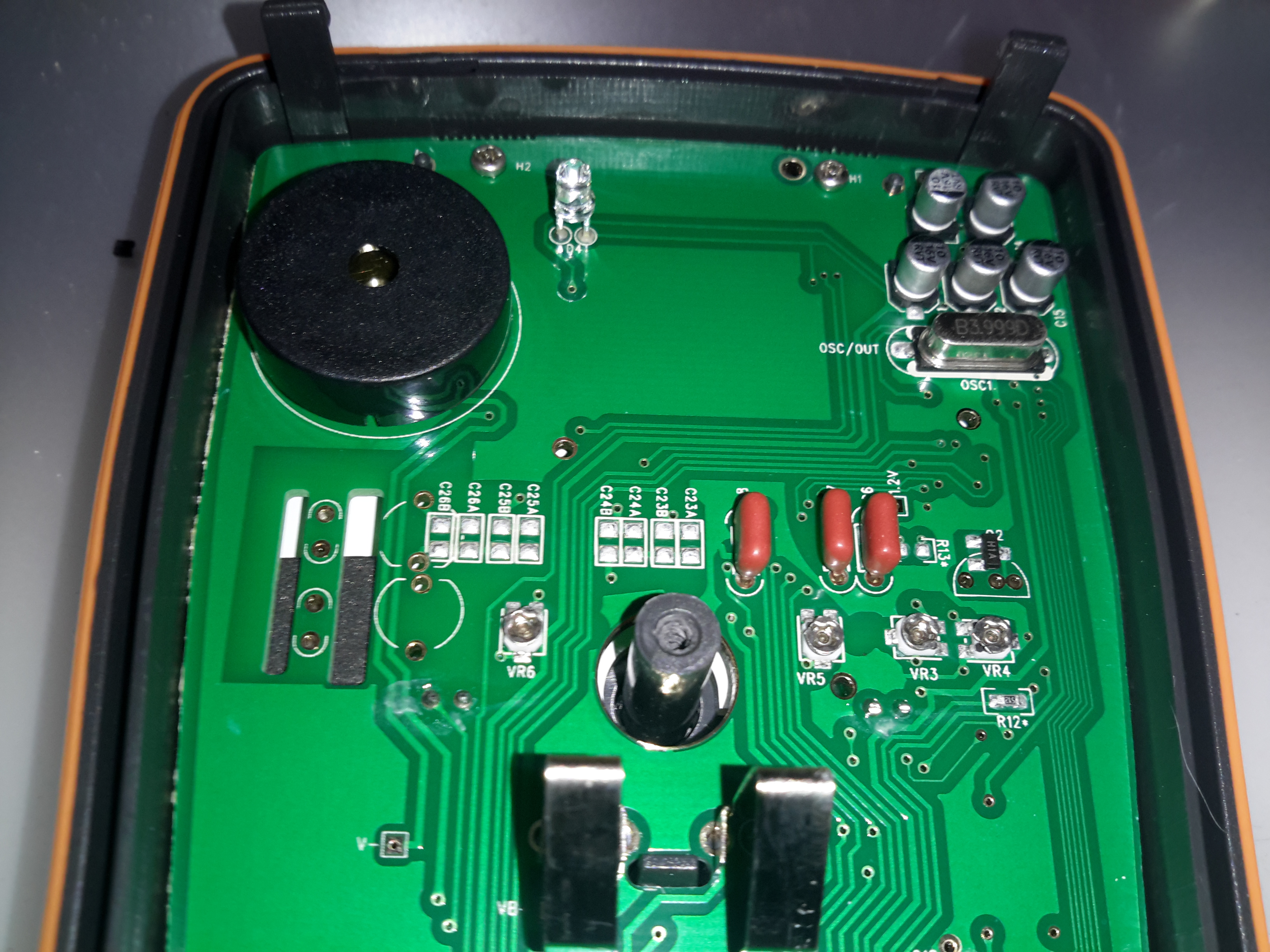
PCB Rear Top
Not much at the other side of the board, there’s the IR LED for the RS232 interface & the beeper.
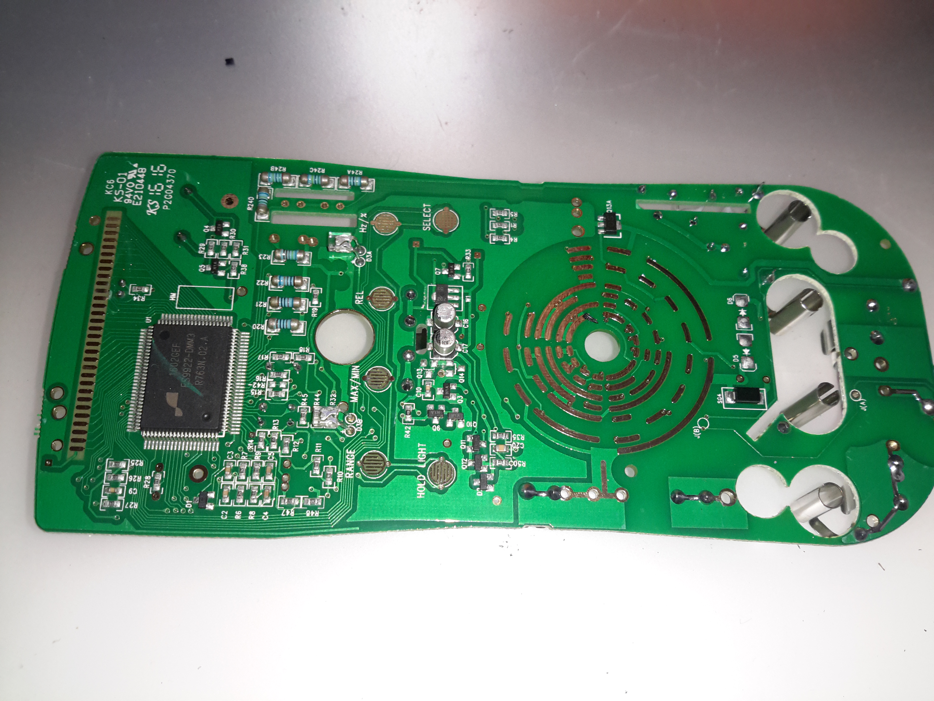
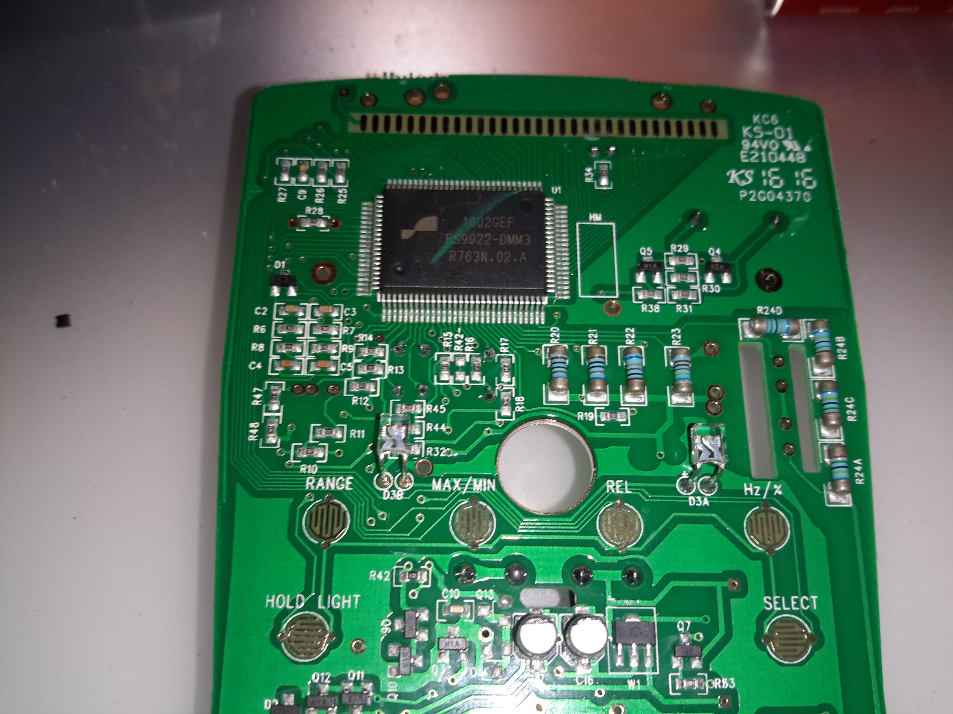
PCB Front
Most of the other components are on the other side of the PCB under the LCD display. The range switch is in the centre, while the main chipset is on the left.
DMM Chipset
The chipset of this meter is a FS9922-DMM3 from Fortune Semiconductor, this is a dedicated DMM chipset with built in ADCs & microcontroller.
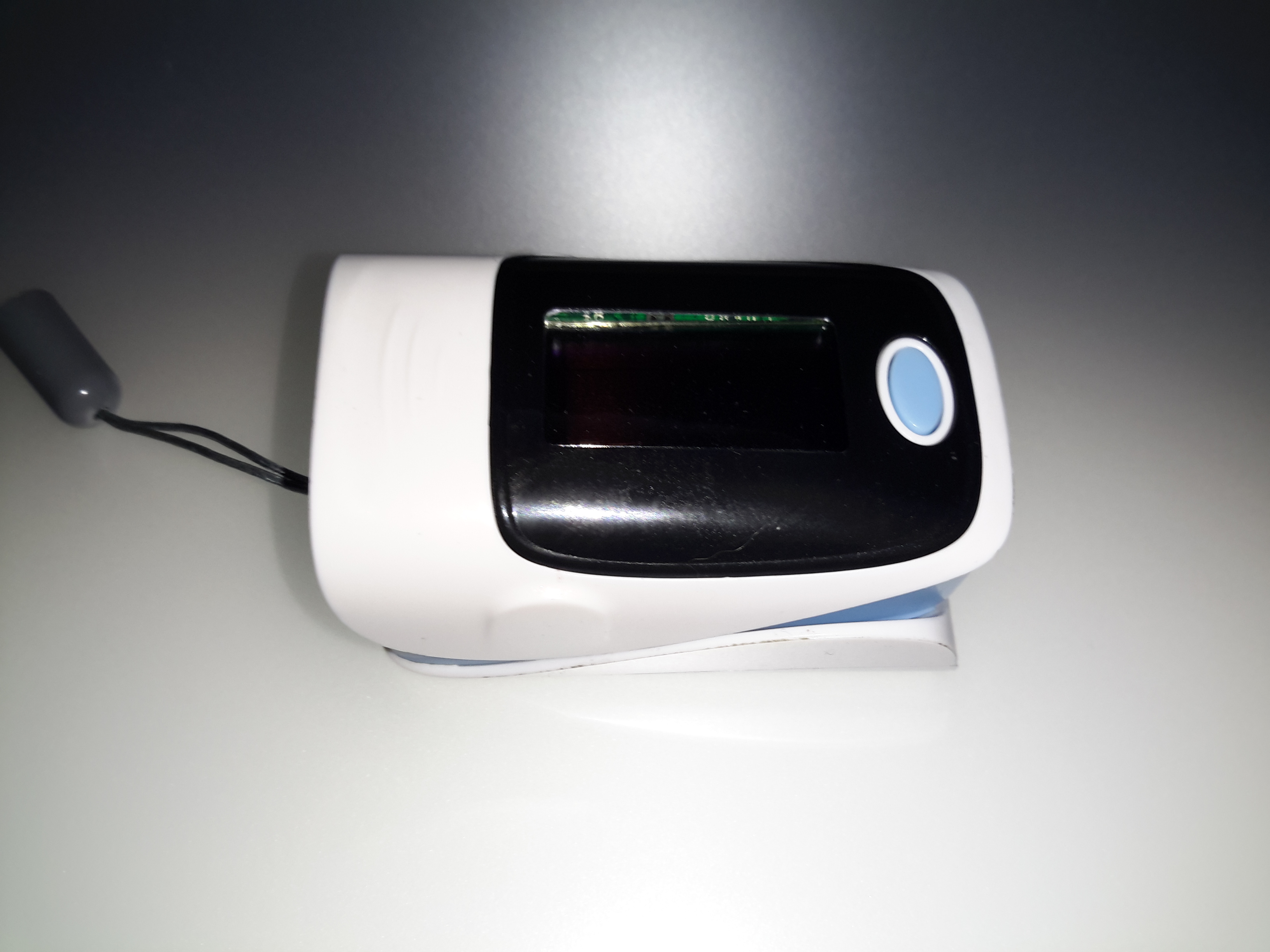
Here’s a piece of medical equipment that in recent years has become extremely cheap, – a Pulse Oximeter, used to determine the oxygen saturation in the blood. These can be had on eBay for less than £15.
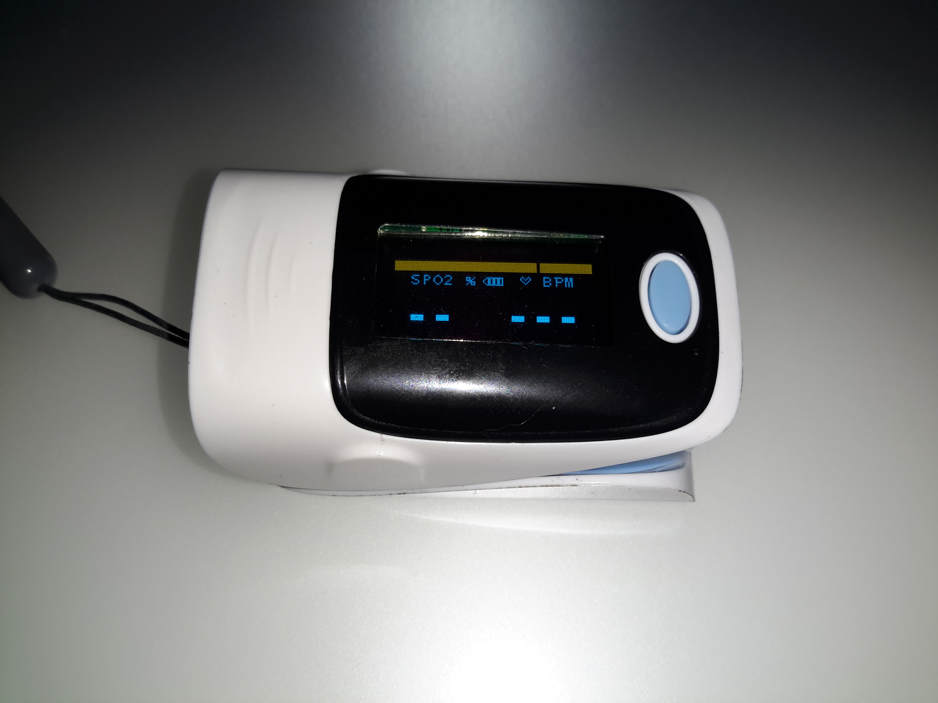
Powered On
This one has a dual colour OLED display, a single button for powering on & adjusting a few settings. These cheap Oximeters do have a bit of a cheap plastic feel to them, but they do seem to work pretty well.
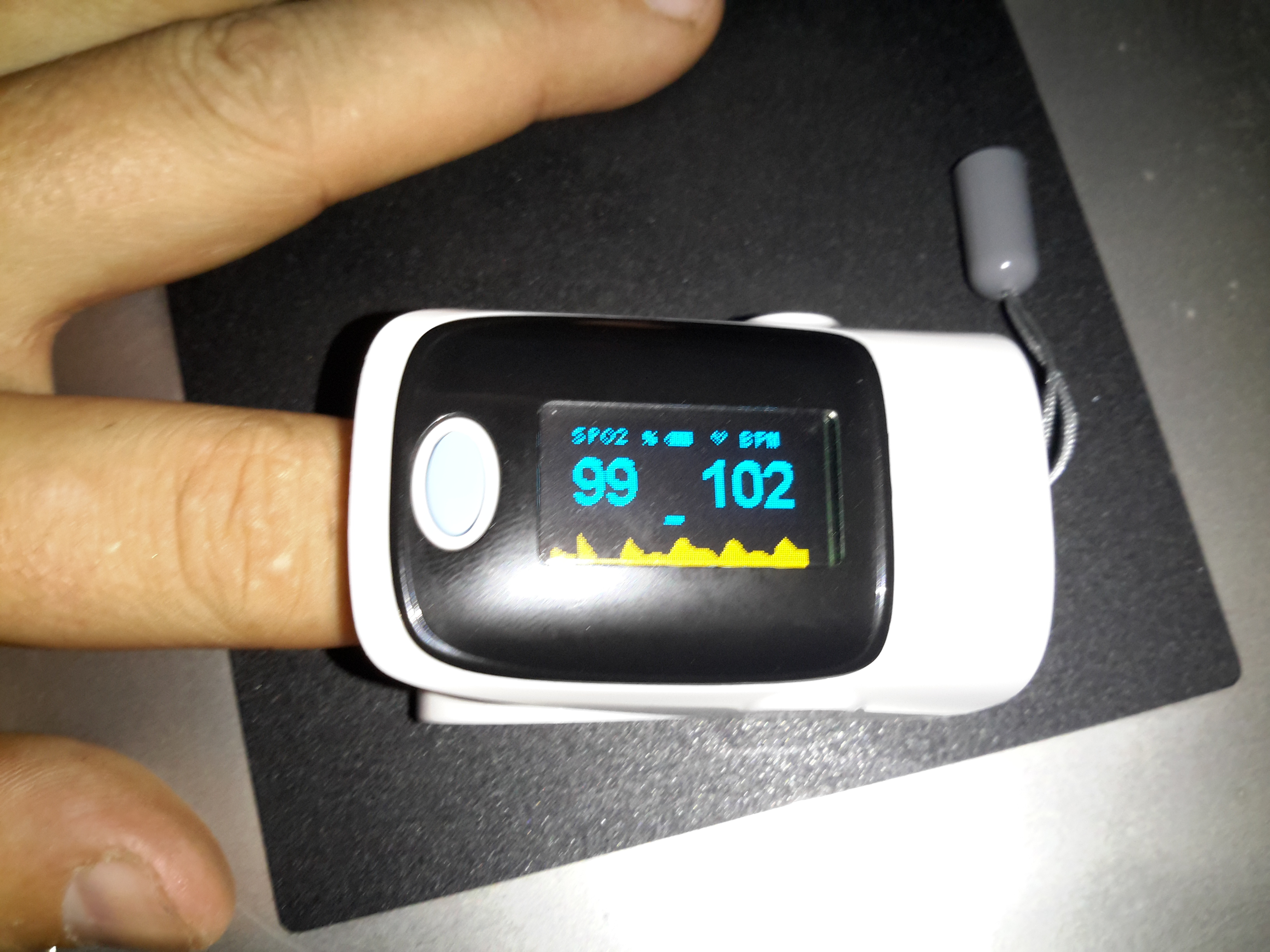
Pulse Oximeter
After a few seconds of being applied to a finger, the unit gives readings that apparently confirm that I’m alive at least. 😉 The device takes a few seconds to get a baseline reading & calibrate the sensor levels.
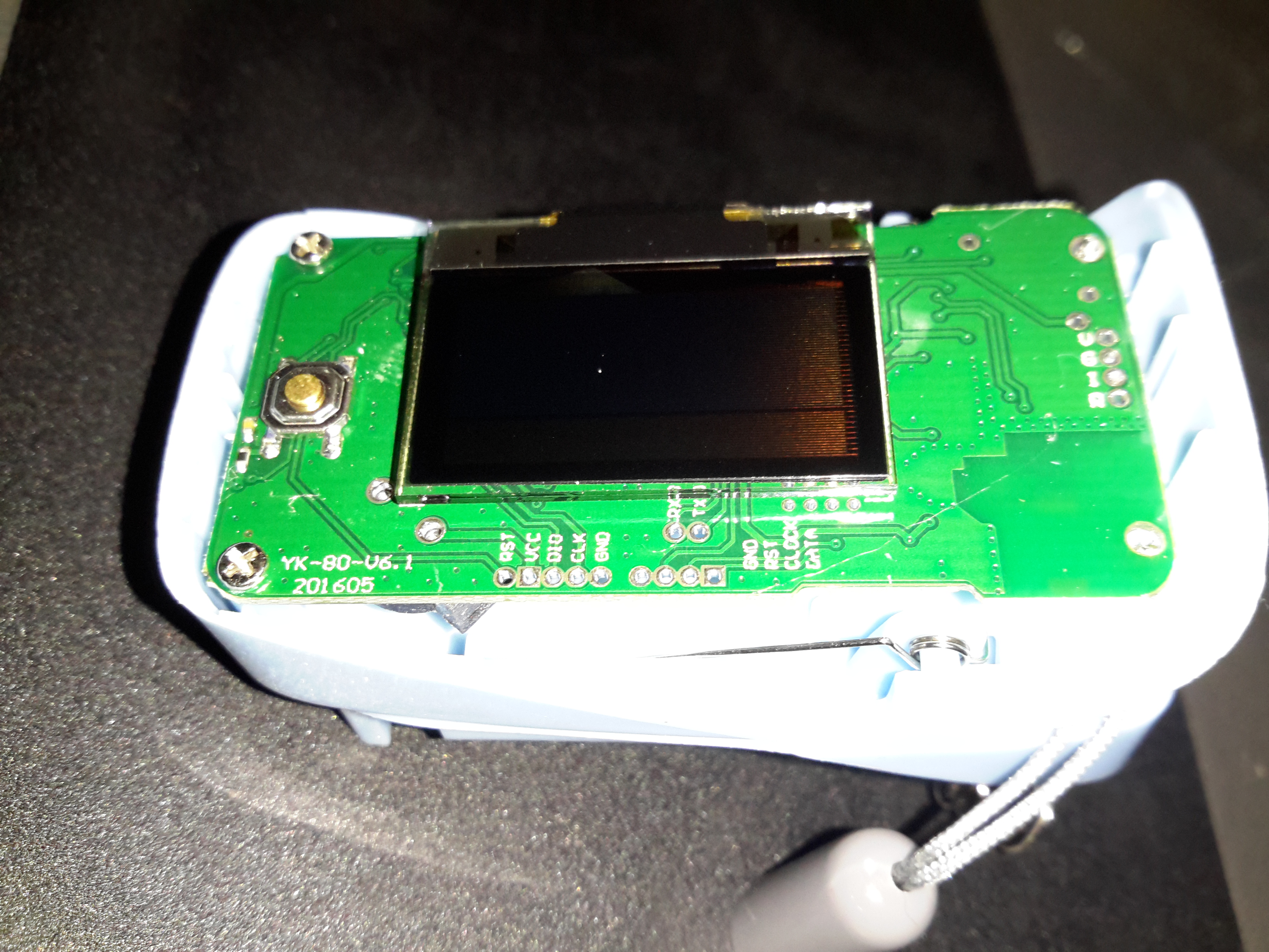
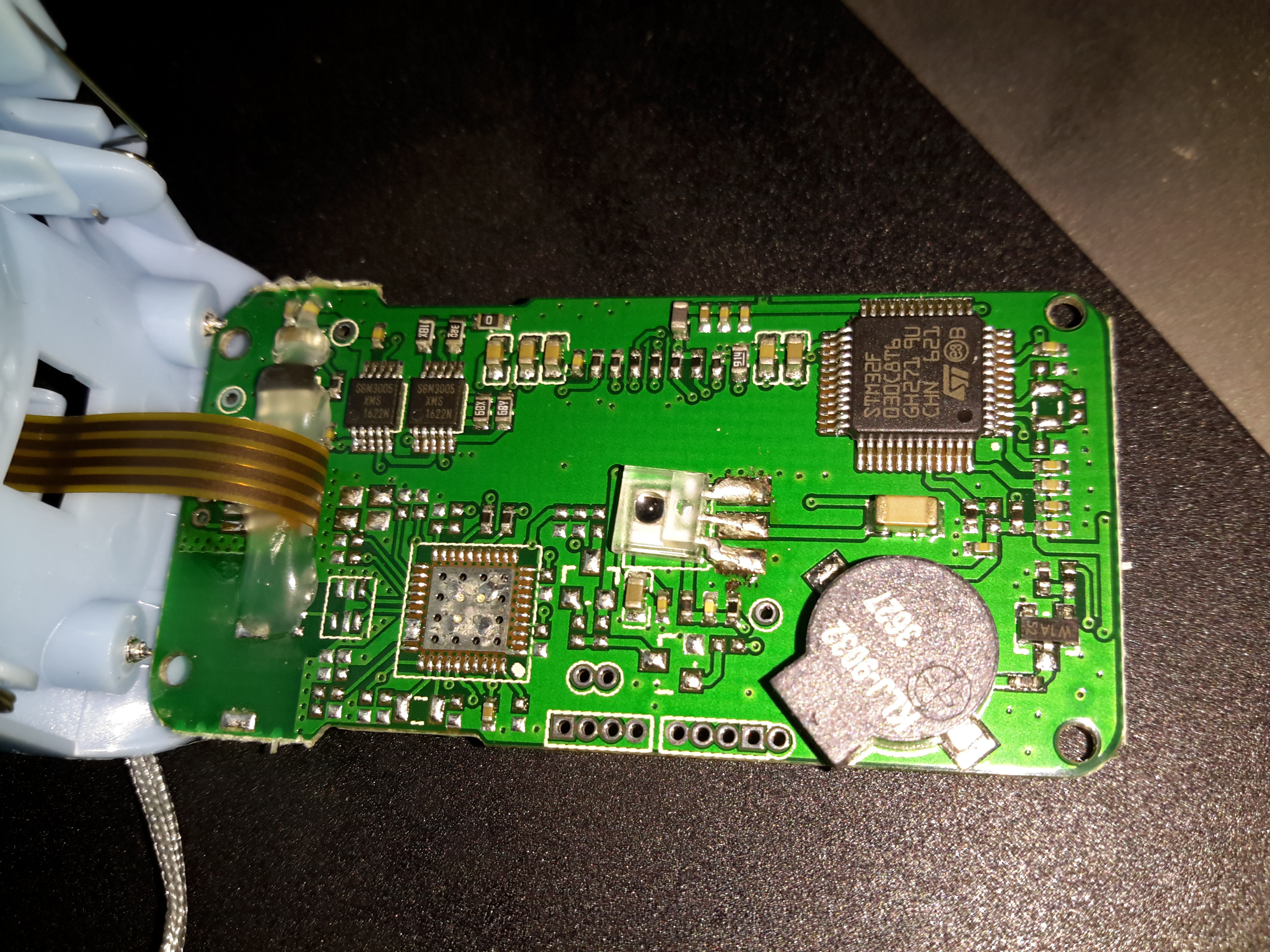
Main PCB Top
The plastic casing is held together with a few very small screws, but comes apart easily. here is the top of the main board with the OLED display panel. There appears to be a programming header & a serial port on the board as well. I’ll have to poke at these pads with a scope to see if any useful data is on the pins.
Main PCB Bottom
The bottom of the board has all the main components of the system. The microcontroller is a STM32F03C8T6, these are very common in Chinese gear these days. There’s a small piezo beeper & the main photodiode detector is in the centre.
There is an unpopulated IC space on the board with room for support components. I suspect this would be for a Bluetooth radio, as there’s a space at the bottom left of the PCB with no copper planes – this looks like an antenna mounting point. (The serial port on the pads is probably routed here, for remote monitoring).
At the top left are a pair of SGM3005 Dual SPDT analogue switches. These will be used to alternate the red & IR LEDs on the other side of the shell.
A 4-core FFC goes off to the other side of the shell, bringing power from the battery & supplying the sensing LEDs.
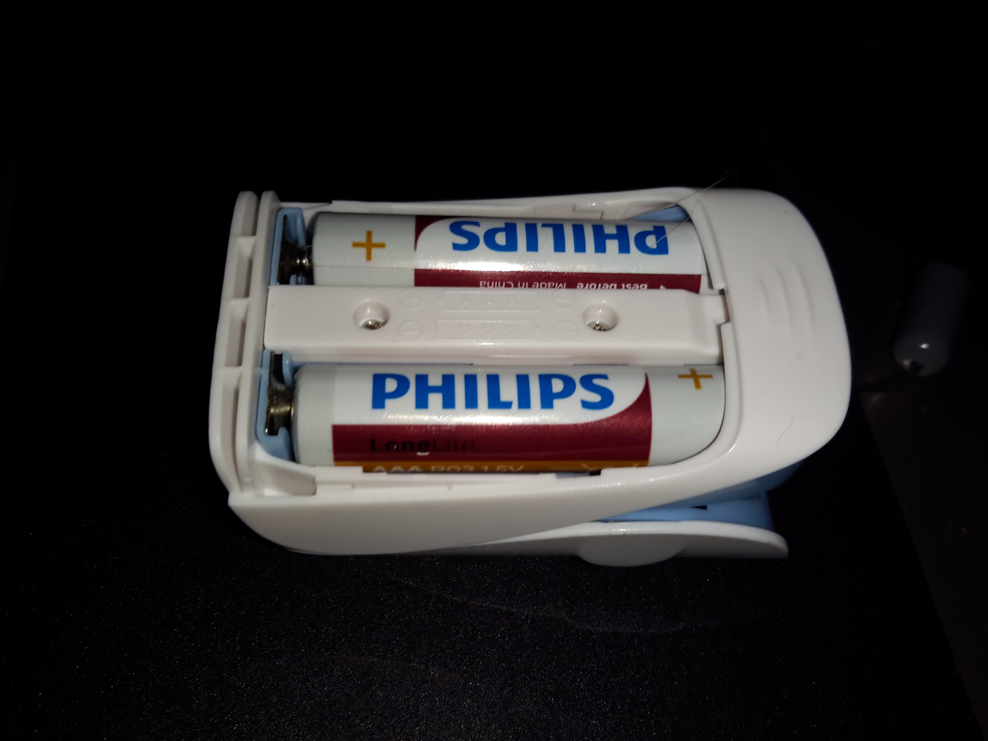
Battery Compartment
Power is supplied by a pair of AAA cells in the other shell.
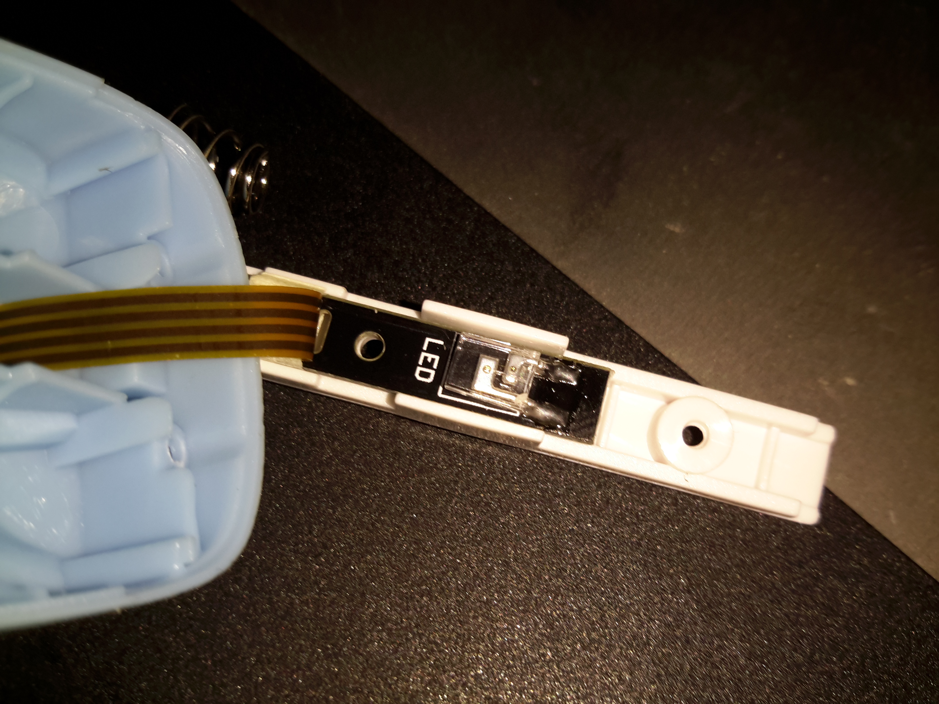
Dual LED
The sensor LEDs are tucked in between the cells, this dual-diode package has a 660nm red LED & a 940nm IR LED.
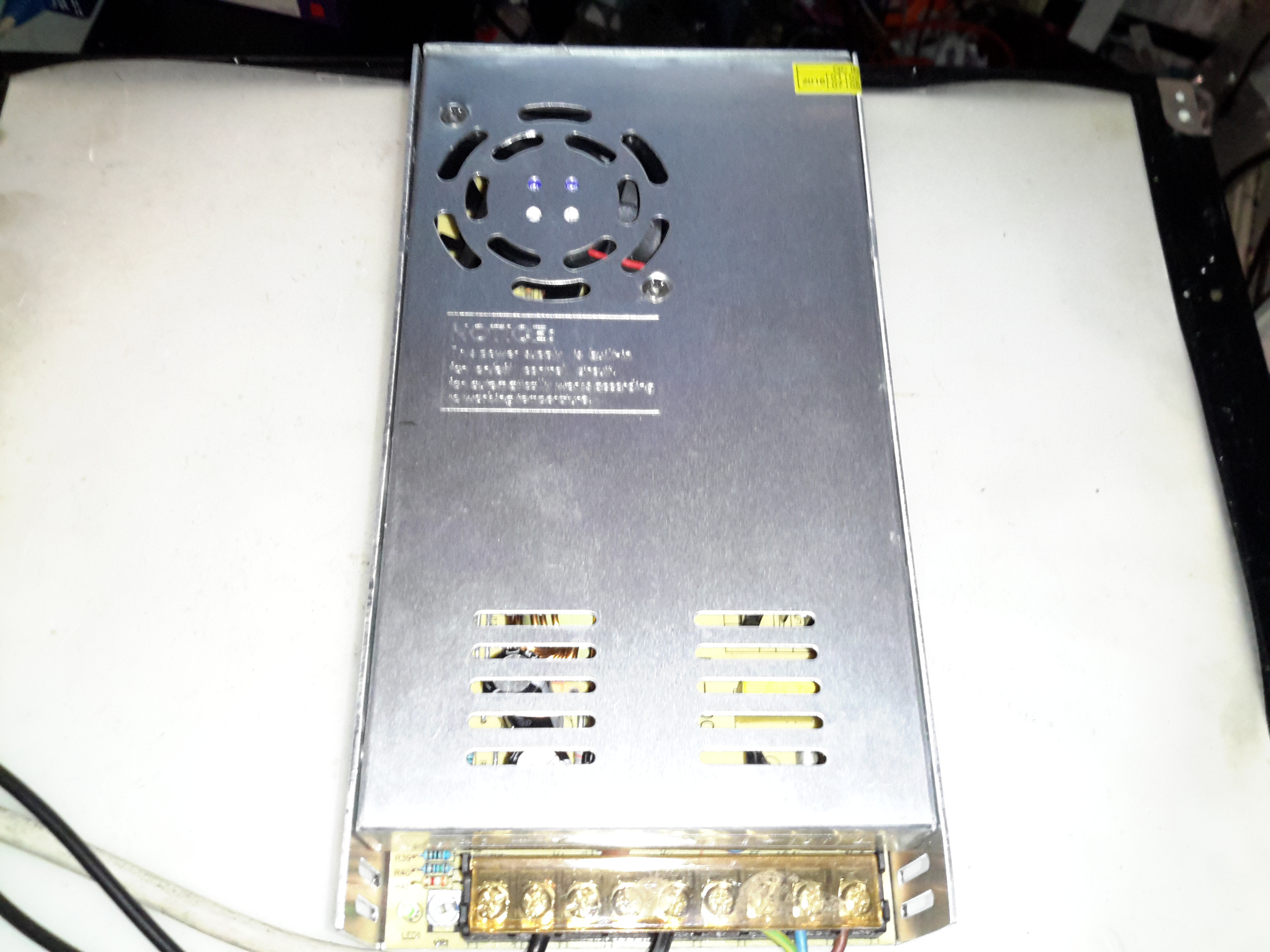
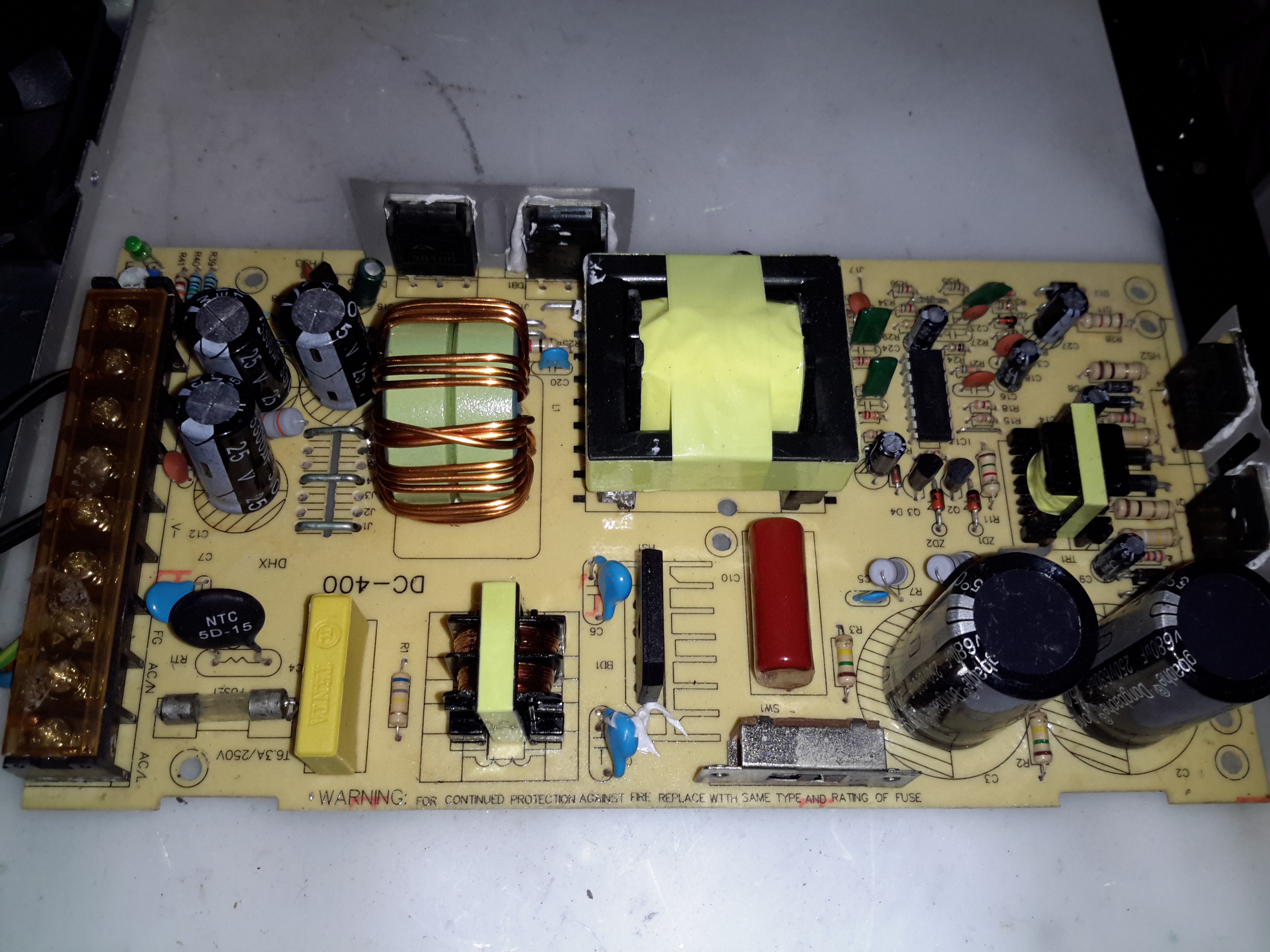
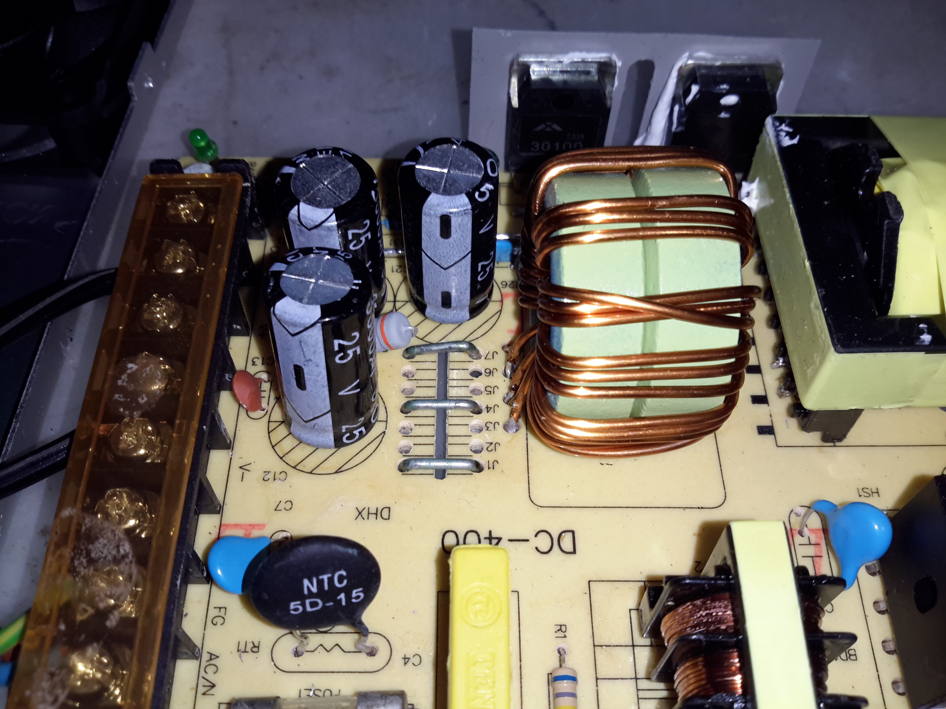
Here’s a cheap PSU from the treasure trove of junk that is eBay, rated at a rather beefy 400W of output at 12v – 33A! These industrial-type PSUs from name brands like TDK-Lambda or Puls are usually rather expensive, so I was interested to find out how much of a punishment these cheap Chinese versions will take before grenading. In my case this PSU is to be pushed into float charging a large lead acid battery bank, which when in a discharged state will try to pull as many amps from the charger as can be provided.
Rating Label
These PSUs are universal input, voltage adjustable by a switch on the other side of the PSU, below. The output voltage is also trimmable from the factory, an important thing for battery charging, as the output voltage needs to be sustained at 13.8v rather than the flat 12v from the factory.
Input Voltage SelectorMain Terminal Block
Mains connections & the low voltage outputs are on beefy screw terminals. The output voltage adjustment potentiometer & output indicator LED are on the left side.
Cooling Fan
The cooling fan for the unit, which pulls air through the casing instead of blowing into the casing is a cheap sleeve bearing 60mm fan. No surprises here. I’ll probably replace this with a high-quality ball-bearing fan, to save the PSU from inevitable fan failure & overheating.
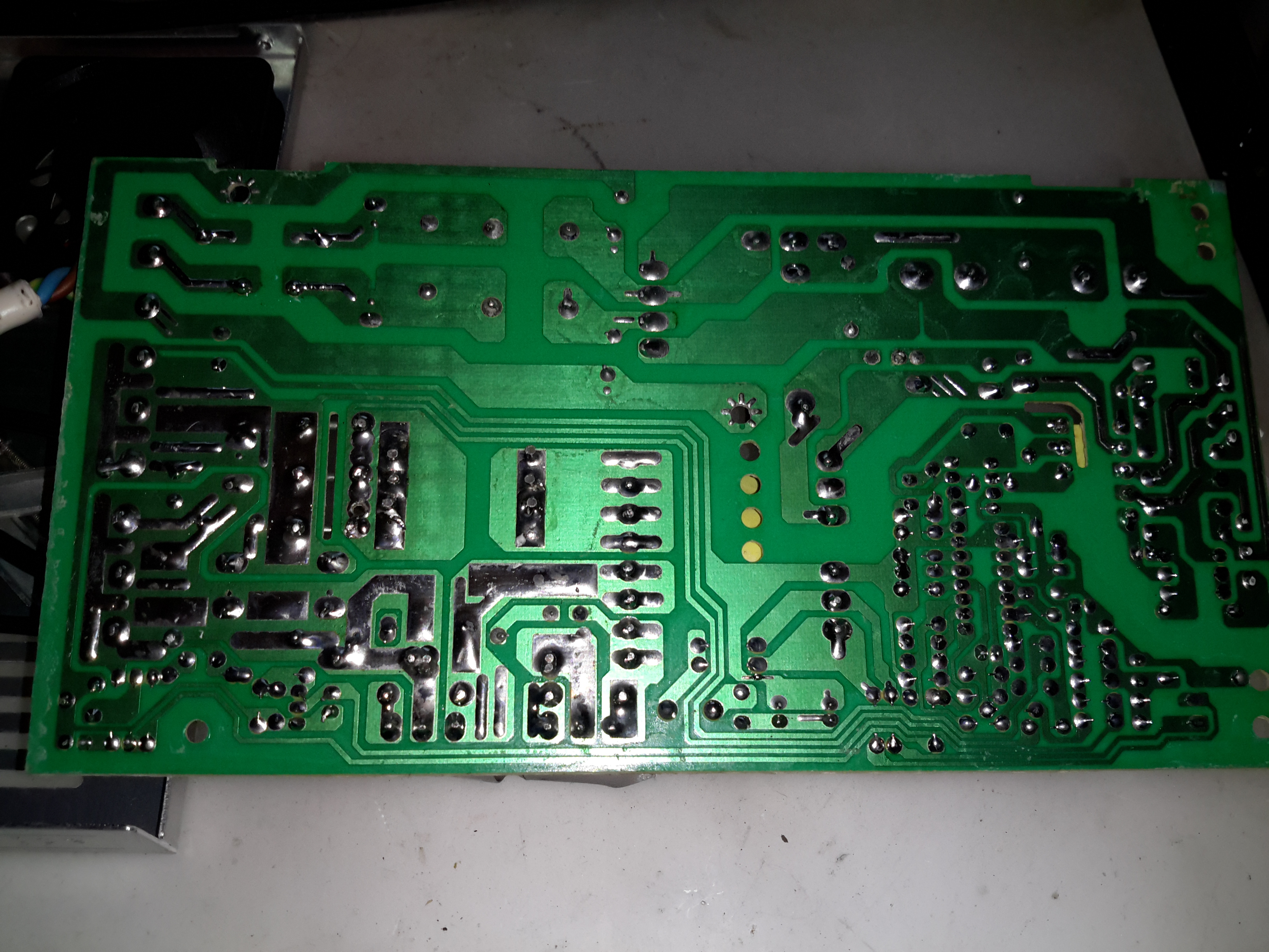
PCB Bottom
The PCB tracks are generously laid out on the high current output side, but there are some primary/secondary clearance issues in a couple of places. Lindsay Wilson over at Imajeenyus.com did a pretty thorough work-up on the fineries of these PSUs, so I’ll leave most of the in-depth stuff via a linky. There’s also a modification of this PSU for a wider voltage range, which I haven’t done in this case as the existing adjustment is plenty wide enough for battery charging duty.
Bare PCB
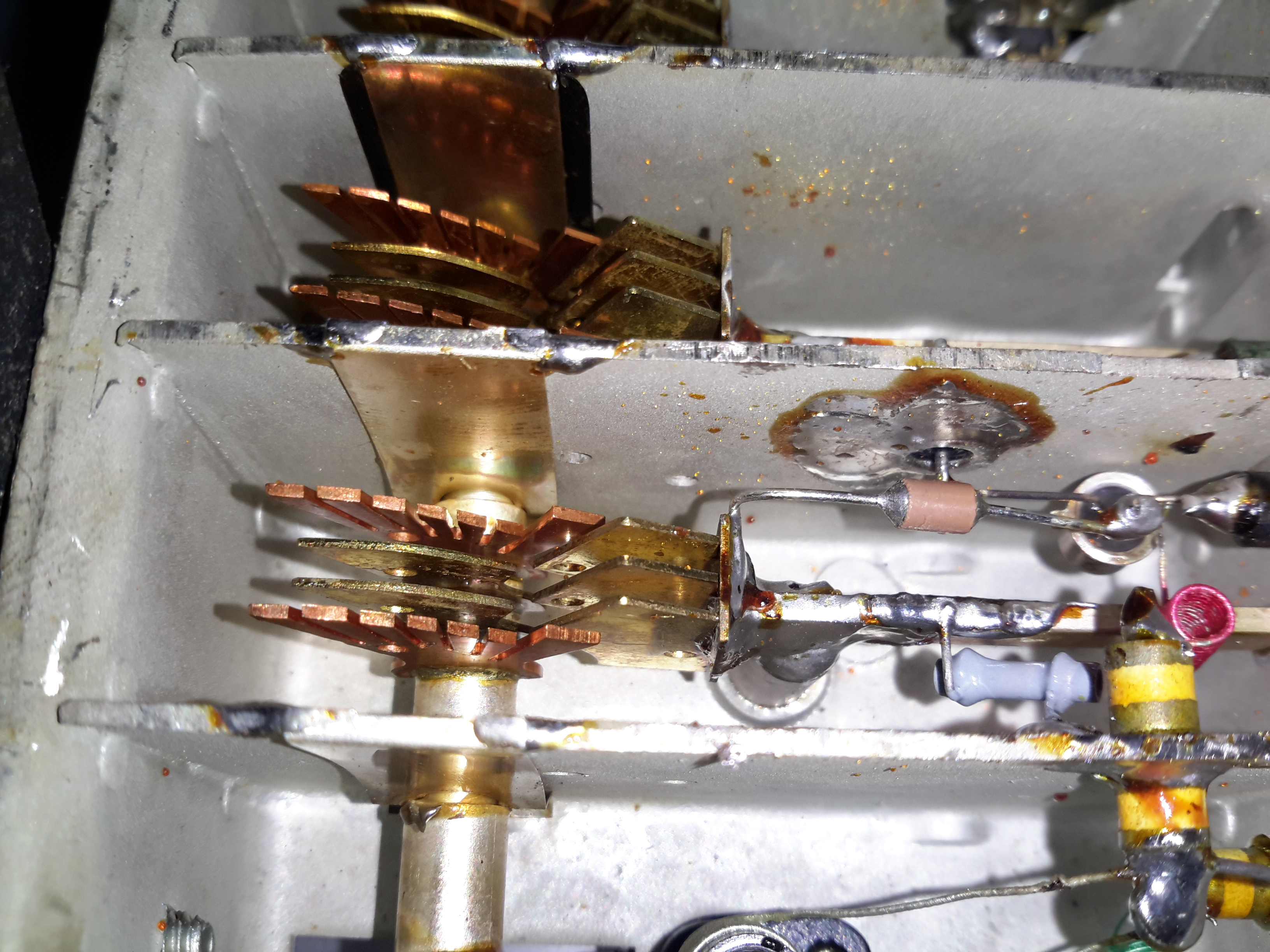
The PCB is laid out in the usual fashion for these PSUs, with the power path taking a U-route across the board. Mains input is lower left, with some filtering. Main diode bridge in the centre, with the voltage selection switch & then the main filter caps. Power is then switched into the transformer by the pair of large transistors on the right before being rectified & smoothed on the top left.
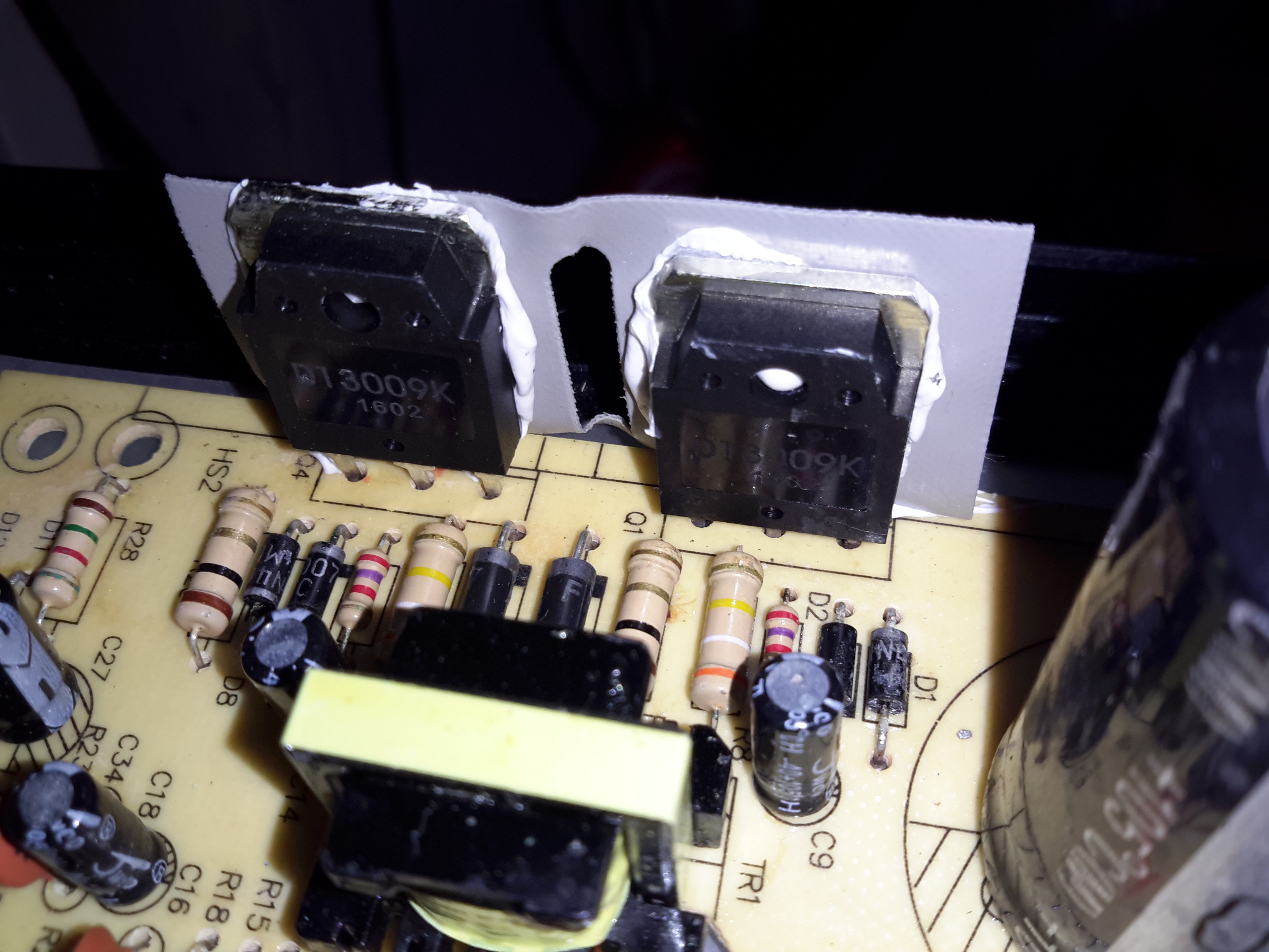
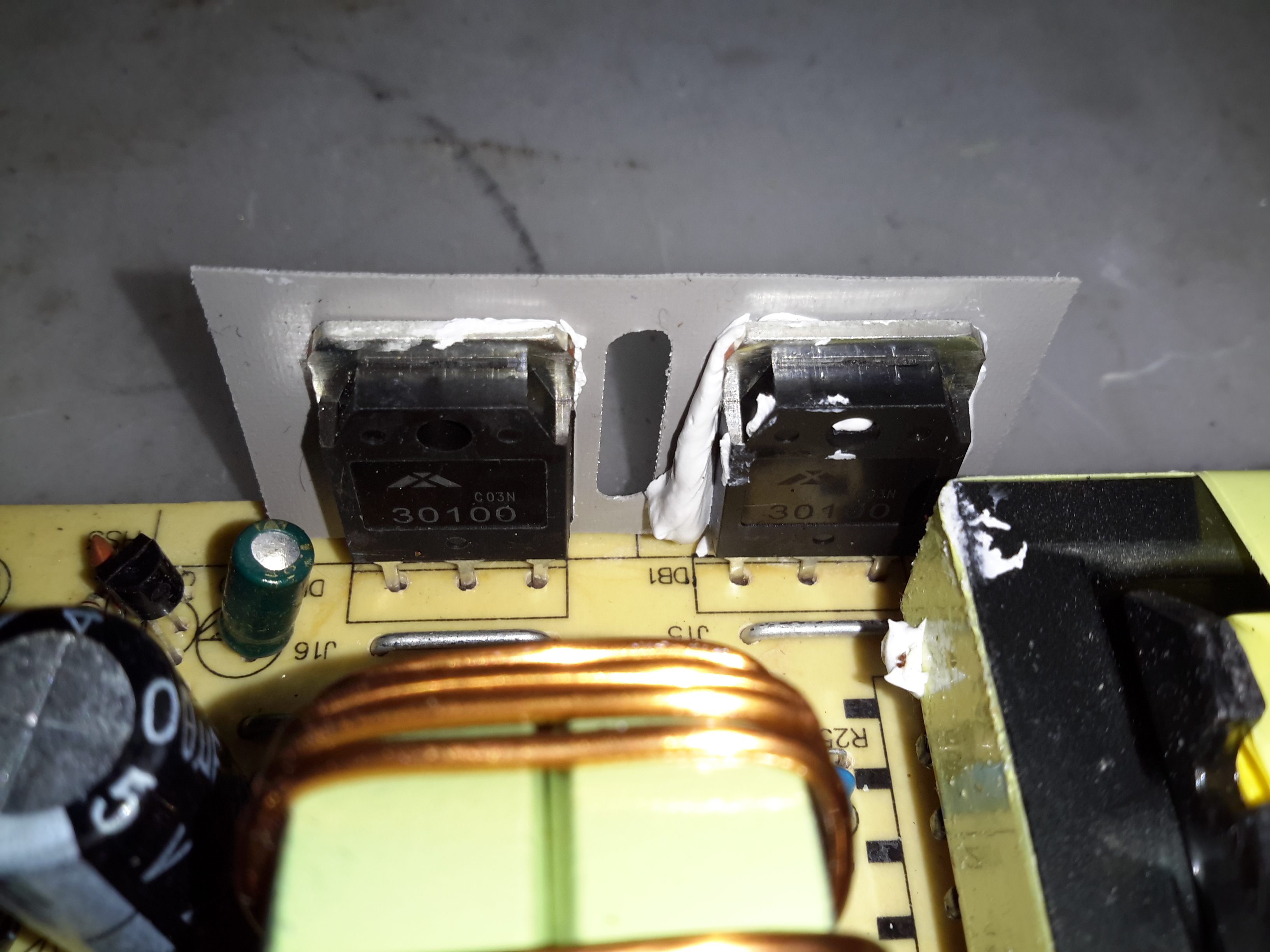
Main Switching Transistors
The pair of main switching devices are mounted to the casing with thermal compound & an insulating pad. To bridge the gap there’s a chunk of aluminium which also provides some extra heatsinking.
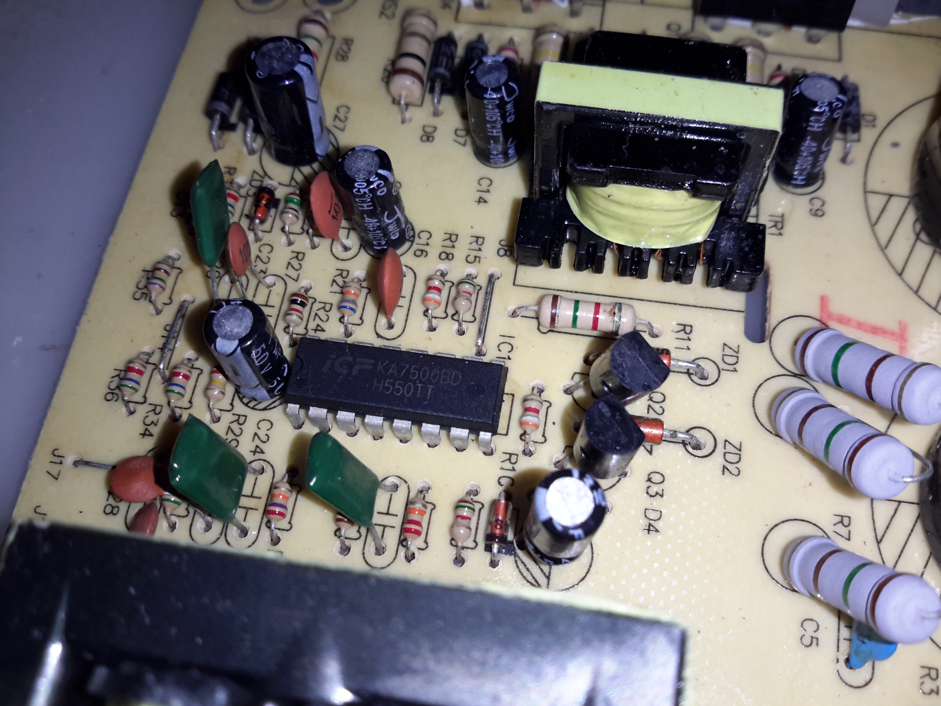
SMPS Drive IC & Base Drive Transformer
The PSU is controlled by a jelly-bean TL494 PWM controller IC. No active PFC in this cheap supply so the power factor is going to be very poor indeed.
Input Protection
Input protection & filtering is rather simple with the usual fuse, MOV filter capacitor & common mode choke.
Main Output Rectifiers
Beefy 30A dual diodes on the DC output side, mounted in the same fashion as the main switching transistors.
Output Current Shunt
Current measurement is done by these large wire links in the current path, selectable for different models with different output ratings.
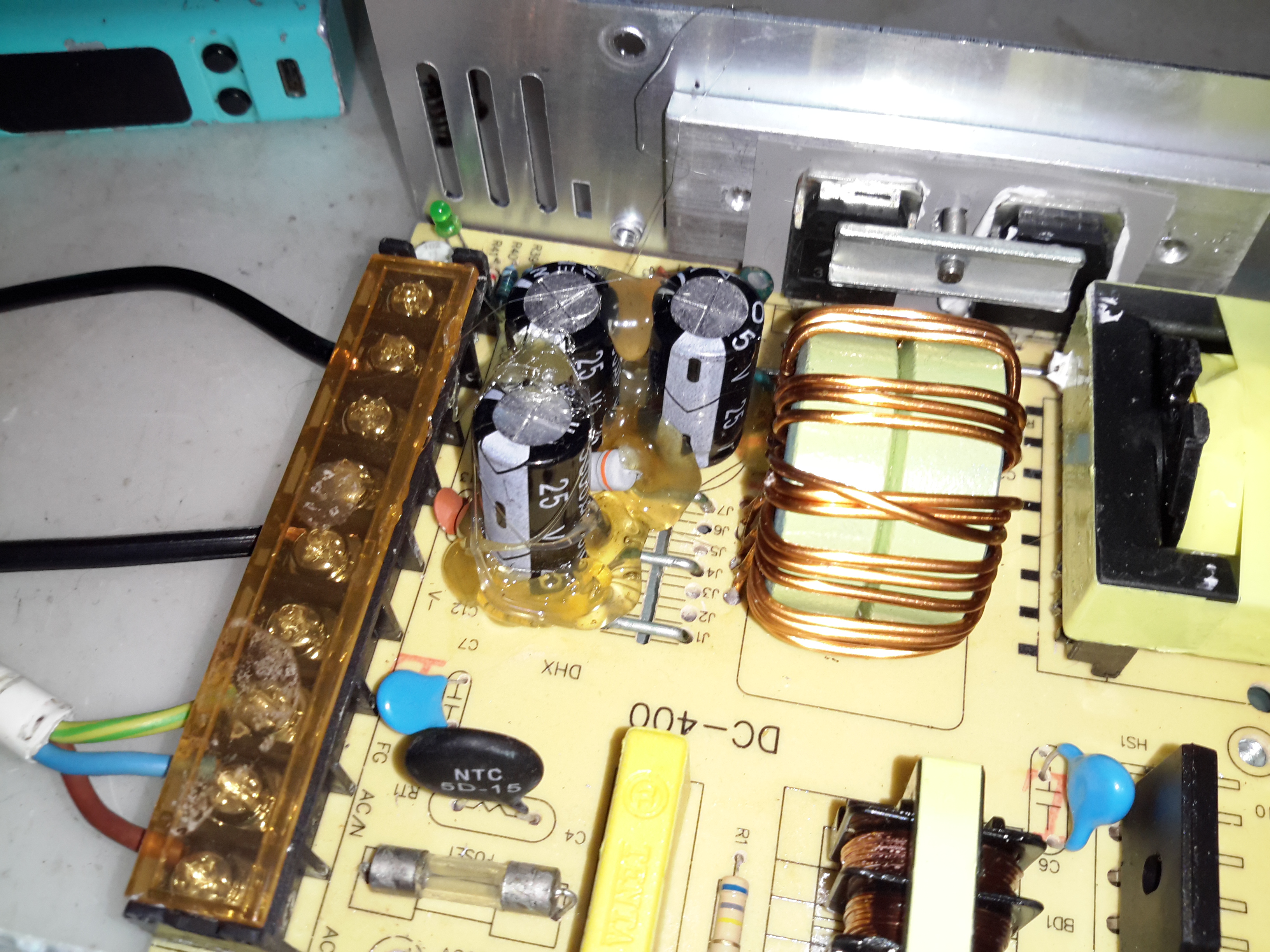
Hot Glue Support
The output capacitors were just floating around in the breeze, with one of them already having broken the solder joints in shipping! After reflowing the pads on all the capacitors some hot glue as flowed around them to stop any further movement.
This supply has now been in service for a couple of weeks at a constant 50% load, with the occasional hammering to recharge the battery bank after a power failure. at 13A the supply barely even gets warm, while at a load high enough to make 40A rated cable get uncomfortably warm (I didn’t manage to get a current reading, as my instruments don’t currently go high enough), the PSU was hot in the power semiconductor areas, but seemed to cope at full load perfectly well.
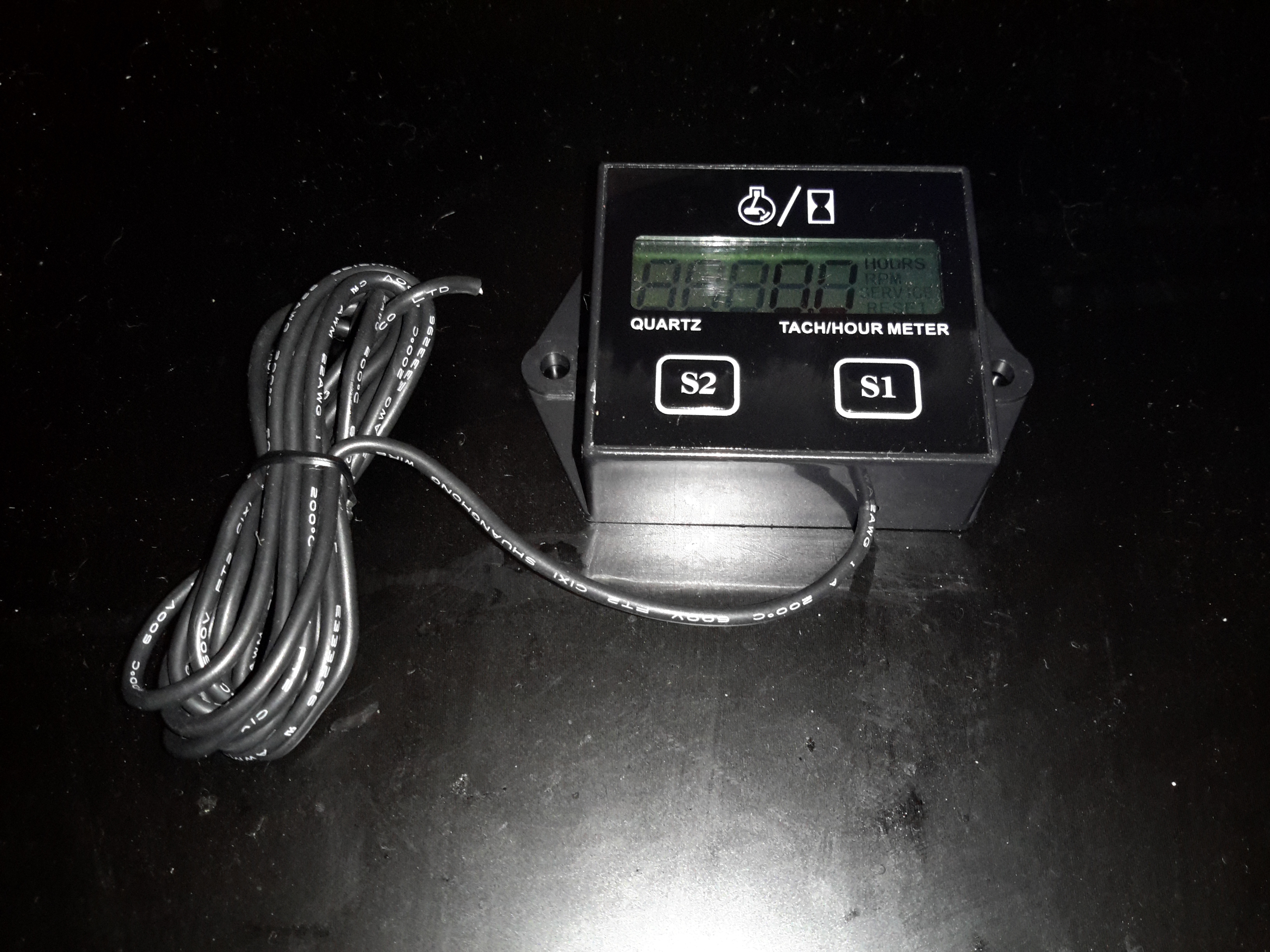
As one of my current projects involves a small petrol engine – a Honda GX35 clone, I figured an hour counter would be very handy to keep an eye on service intervals. (More to come on the engine itself later on). I found a device that would suit my needs on good old eBay.
Inductive Engine Monitor
These engine monitors are pretty cheap, at about £4. The sensing is done by a single heat-resistant silicone wire, that wraps around the HT lead to the spark plug. The unit can be set for different firing intervals via the buttons. In the case of most single-cylinder 4-stroke engines, the spark plug fires on every revolution – wasted-spark ignition. This simplifies the ignition system greatly, by not requiring the timing signal be driven from 1/2 crankshaft speed. The second “wasted” spark fires into the exhaust stroke, so has no effect.
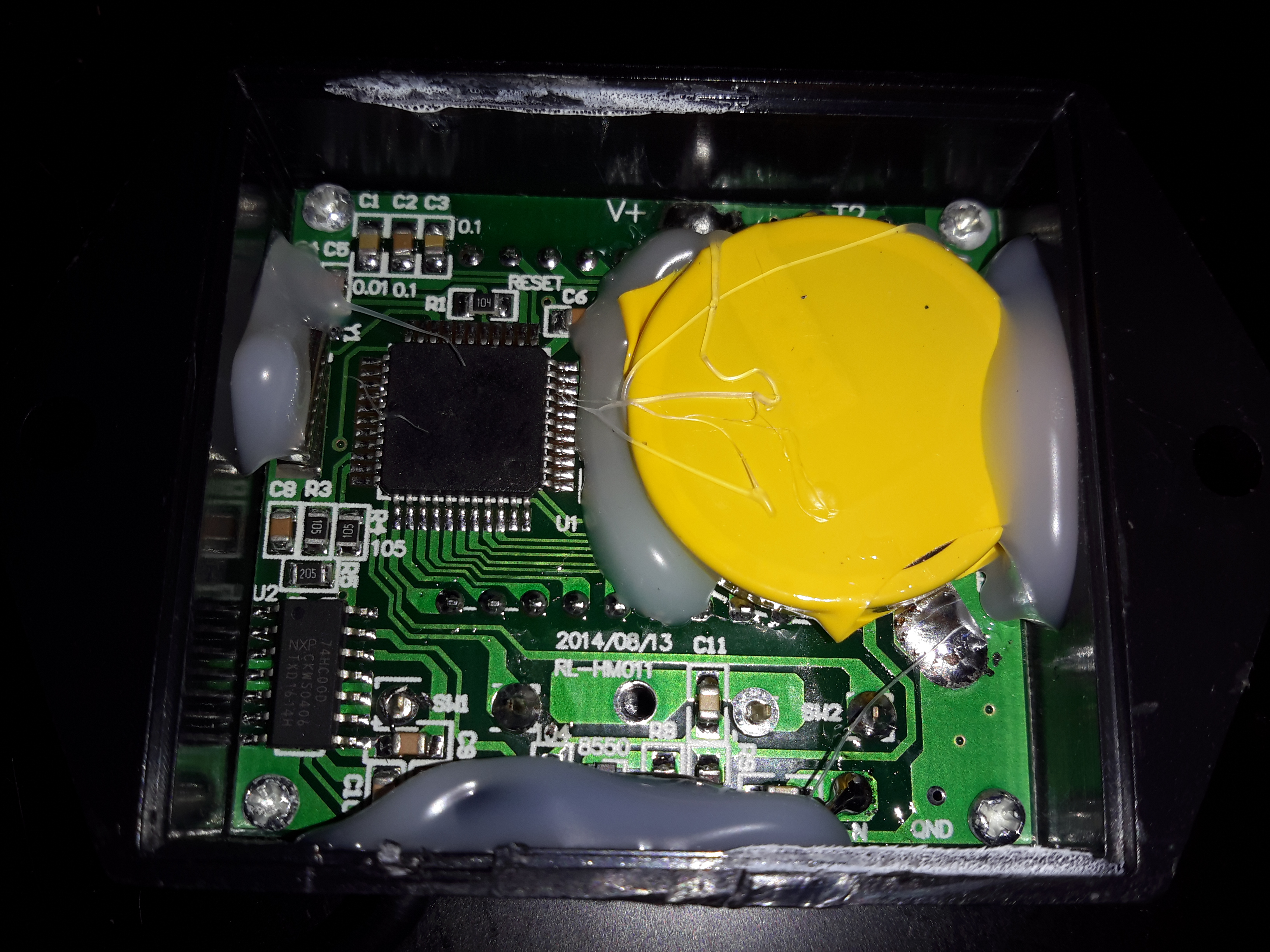
Internals
The back cover is lightly glued into place with a drop of cyanoacrylate in opposite corners, but easily pops off. The power is supplied by a soldered-in 3v Lithium cell. The main microcontroller has no number laser etched on to it at all – it appears it skipped the marking machine.
Input Filtering
The input from the sensing wire comes in through a coupling capacitor & is amplified by a transistor. It’s then fed into a 74HC00D Quad 2-Input NAND gate, before being fed into the microcontroller.
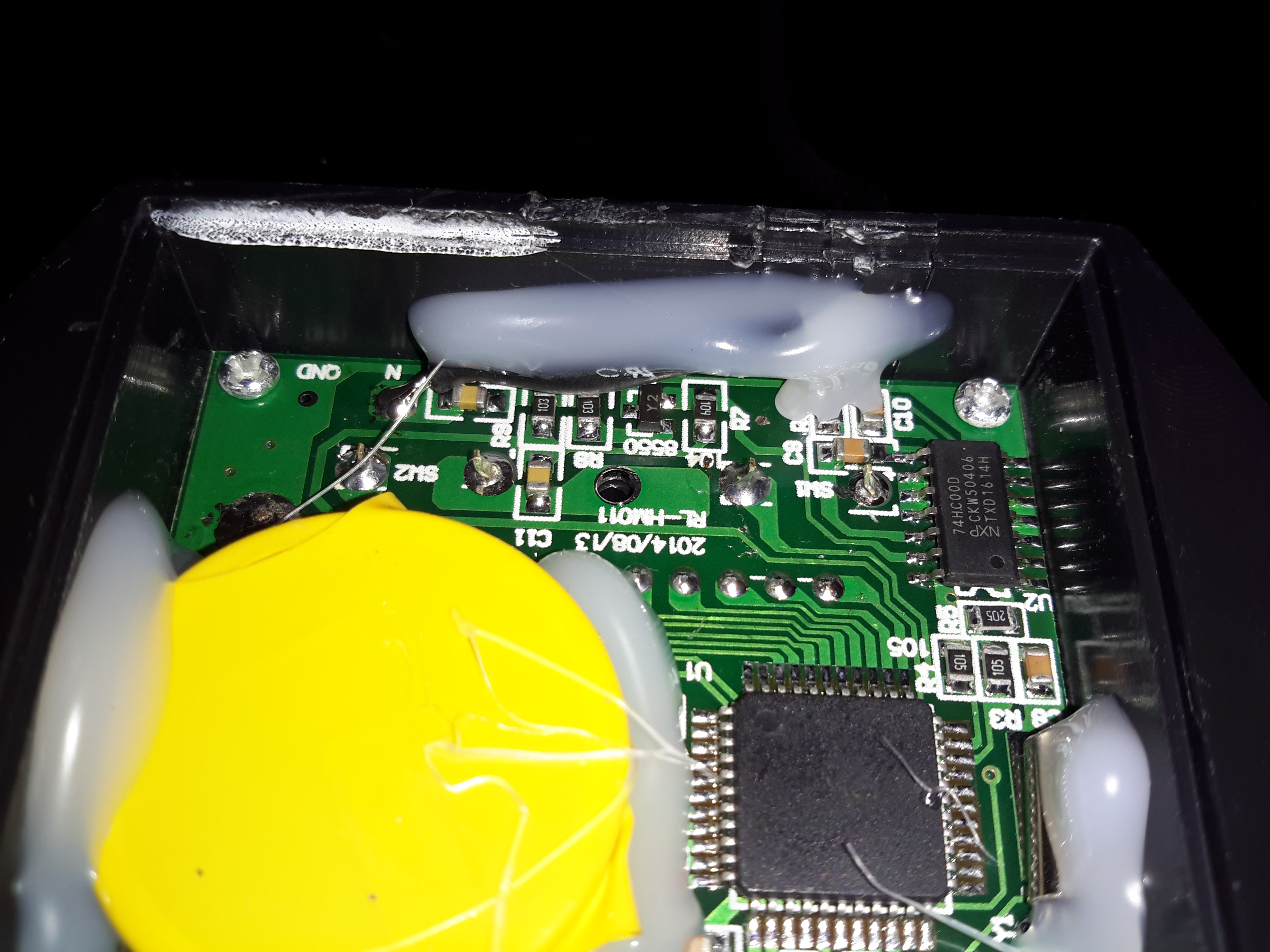
Pickup
The pickup wire is simply wound around the spark plug lead. I’ve held it in position here with some heatshrink tubing. Heat in this area shouldn’t be an issue as it’s directly in the airflow from the flywheel fan.
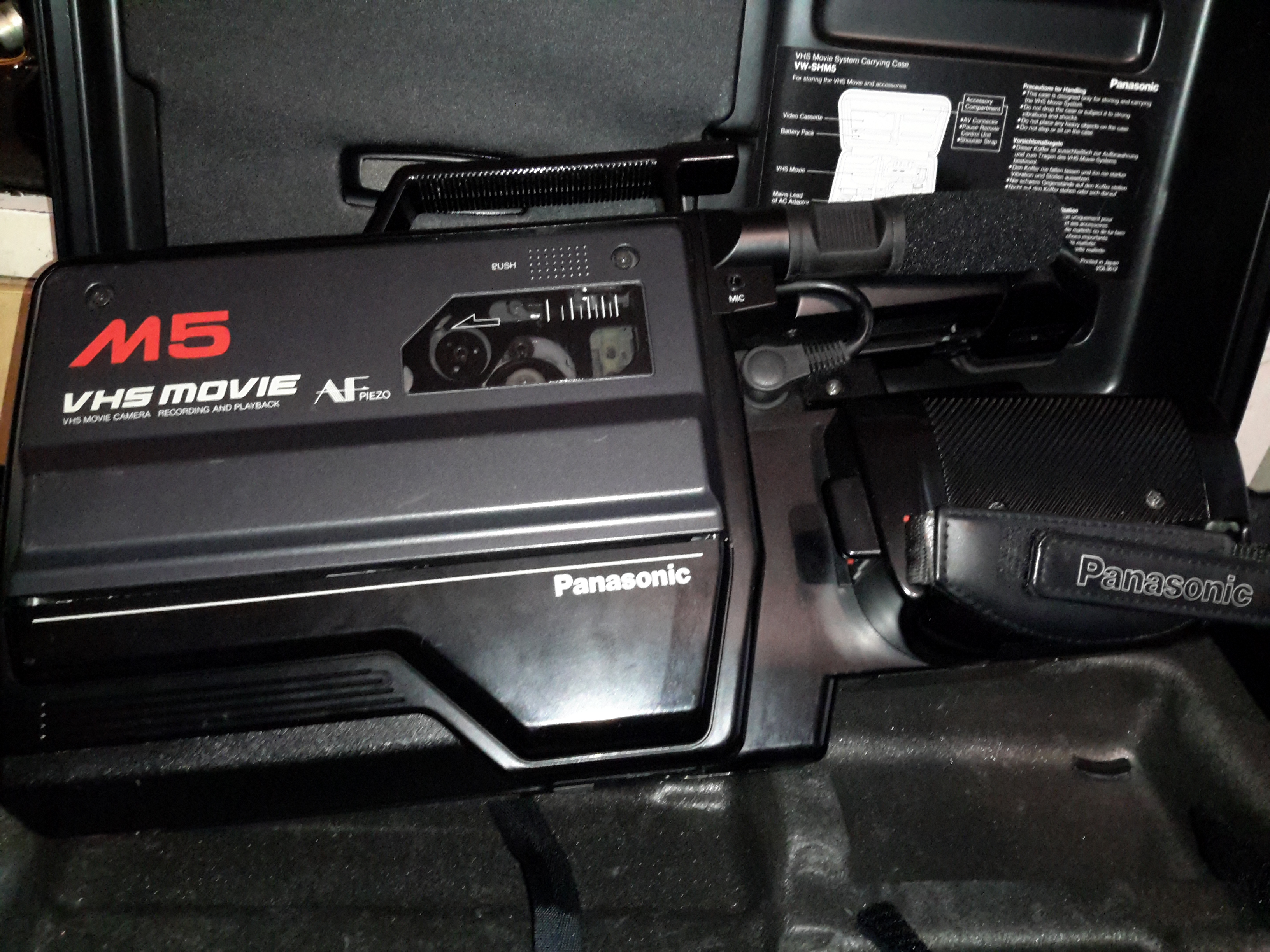
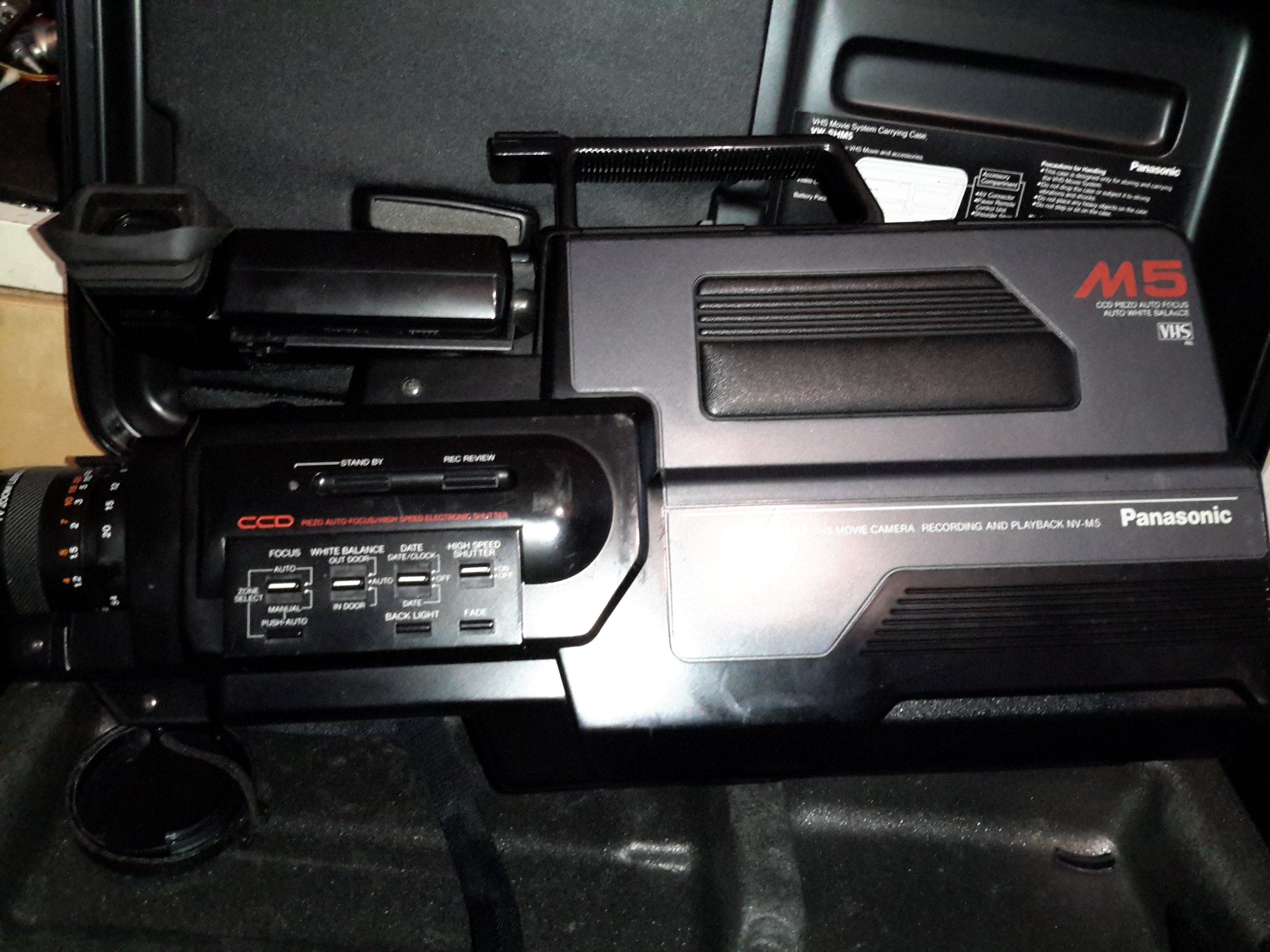
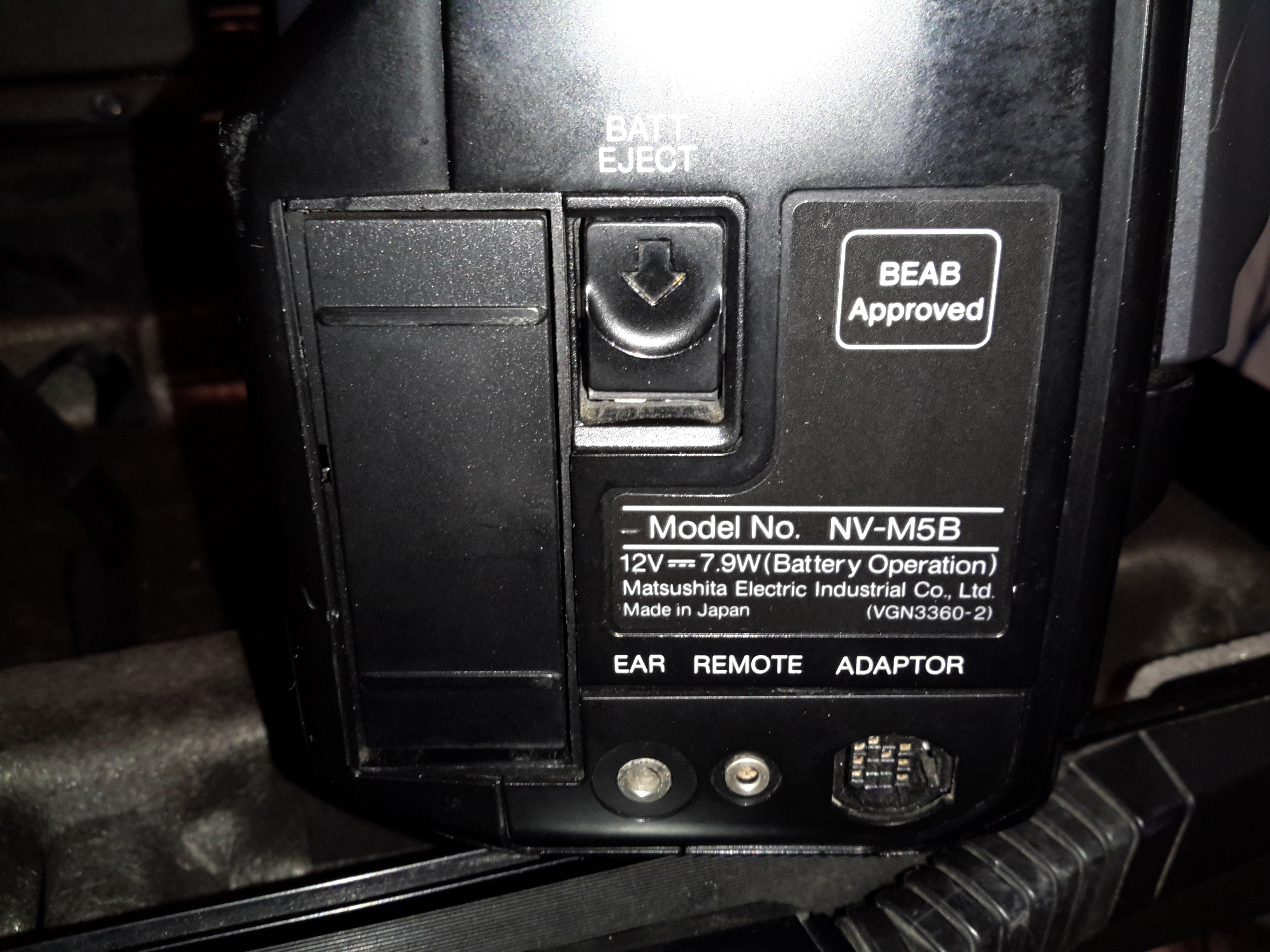
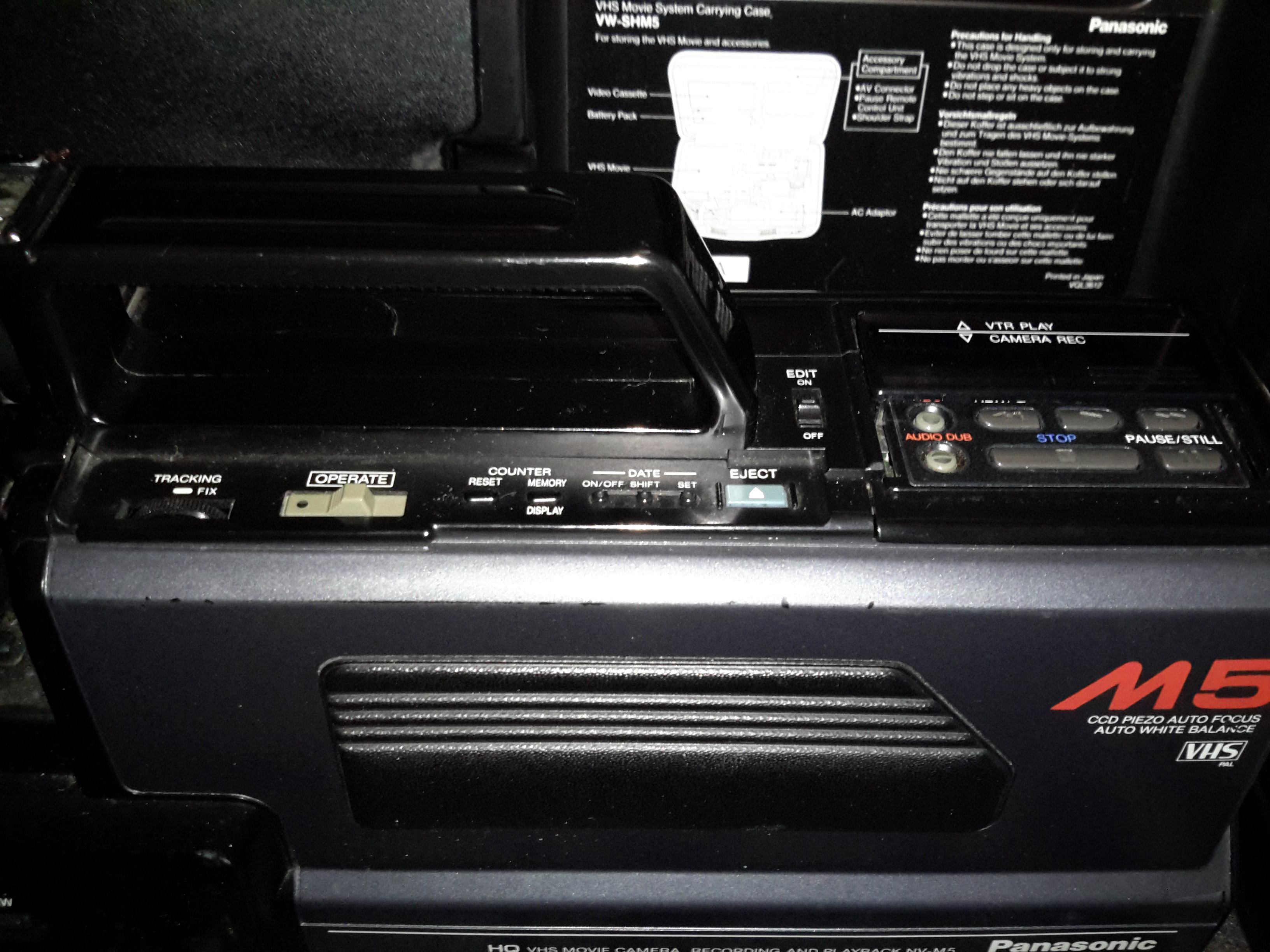
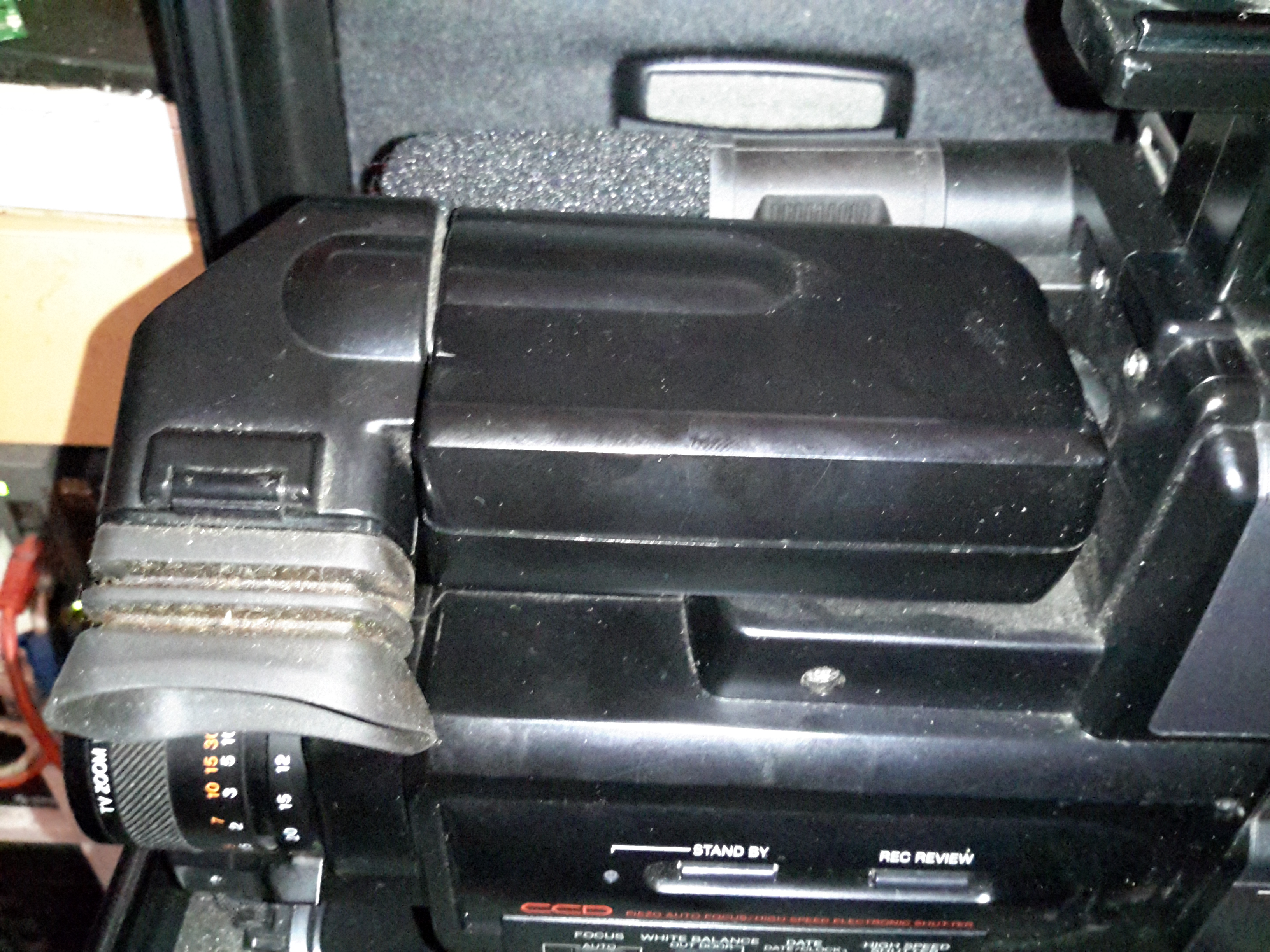
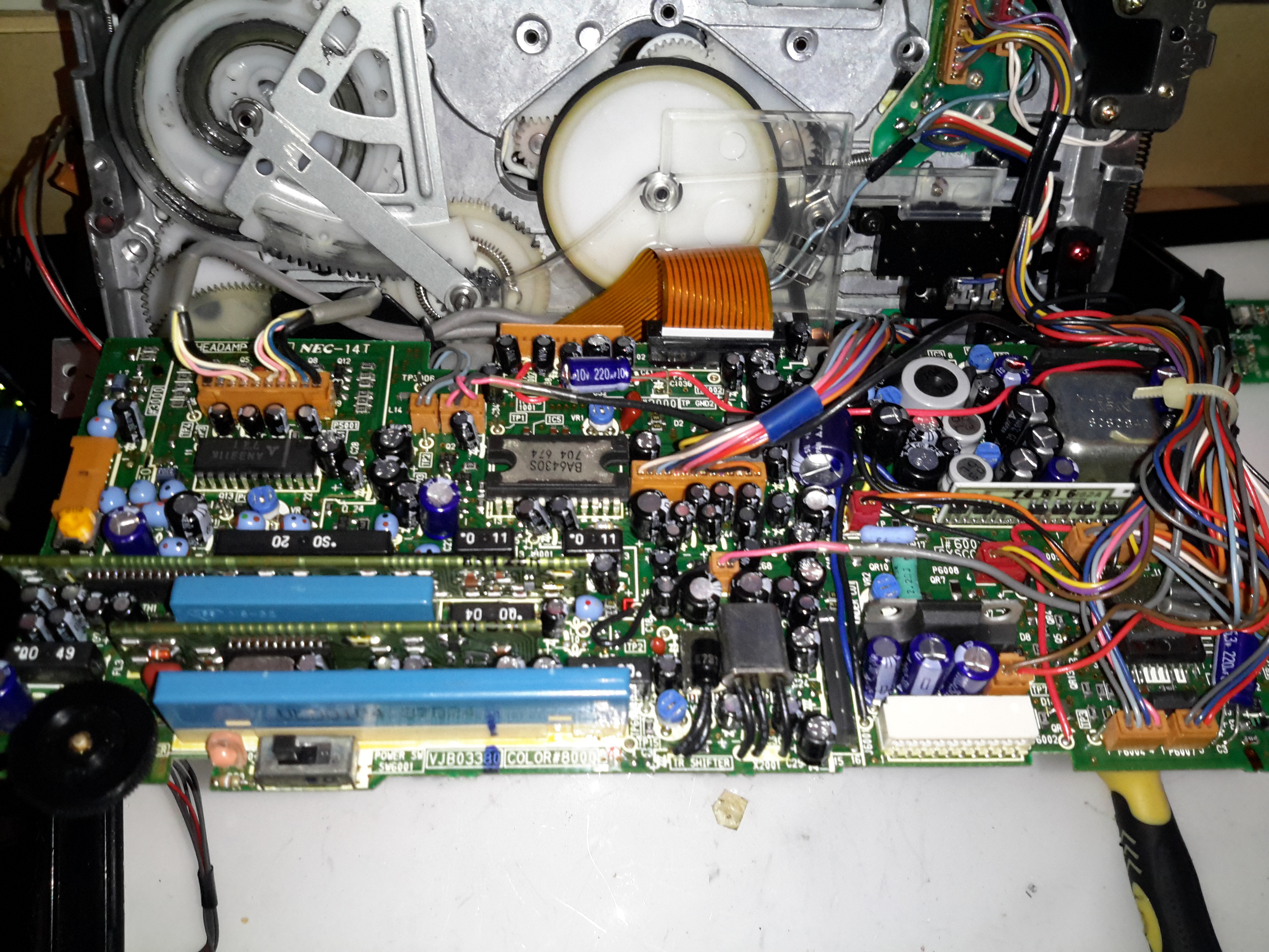
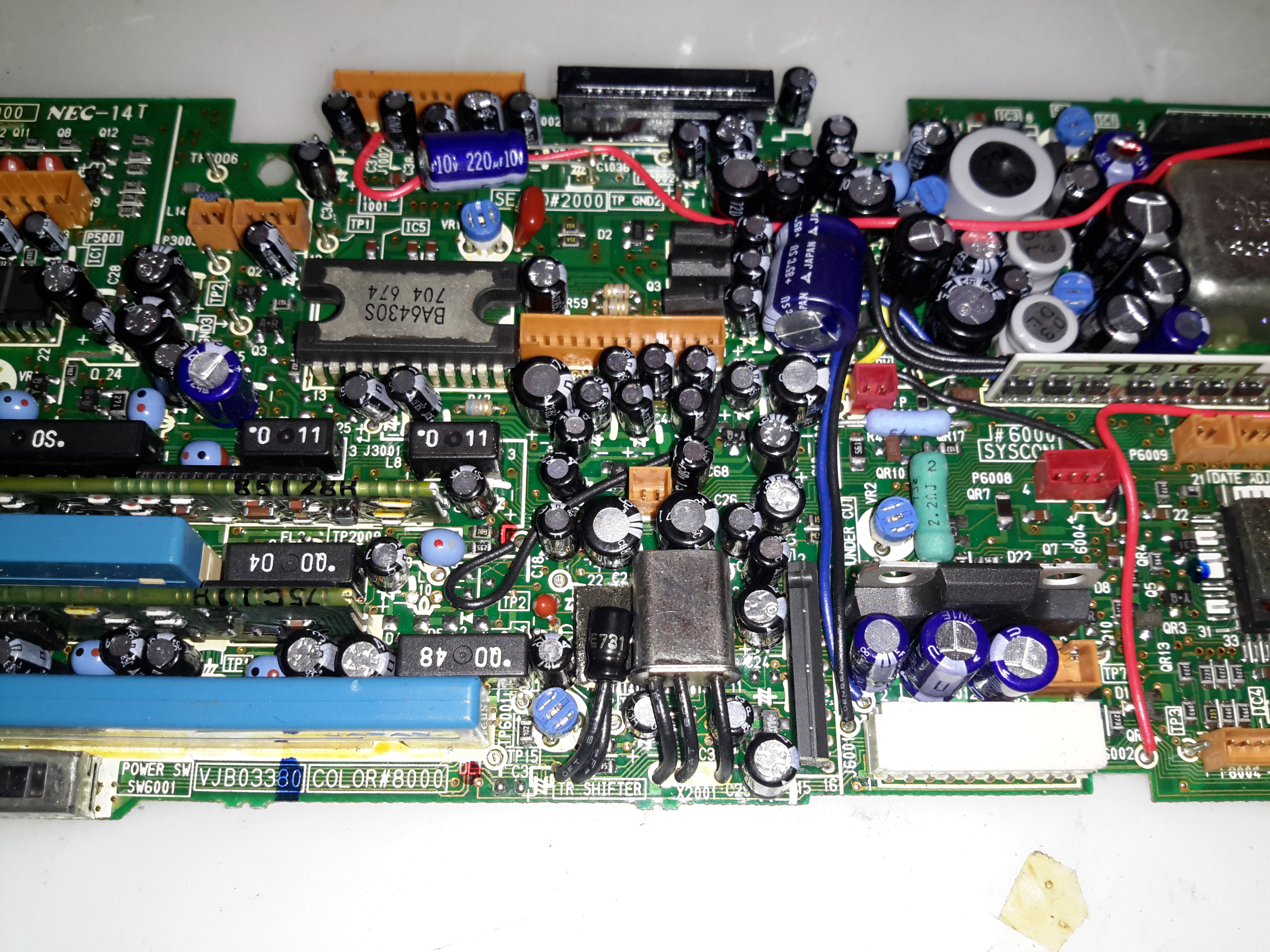
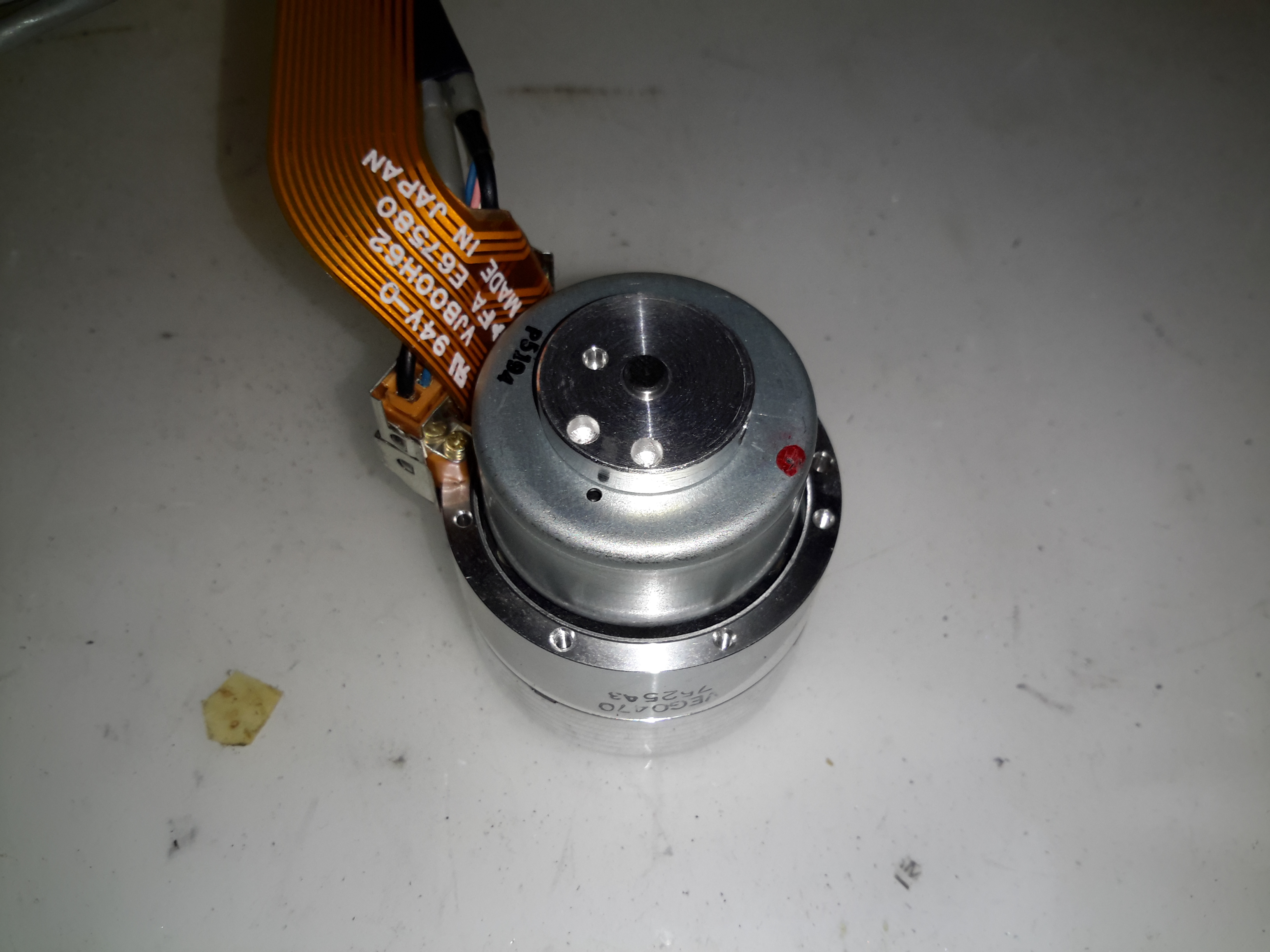
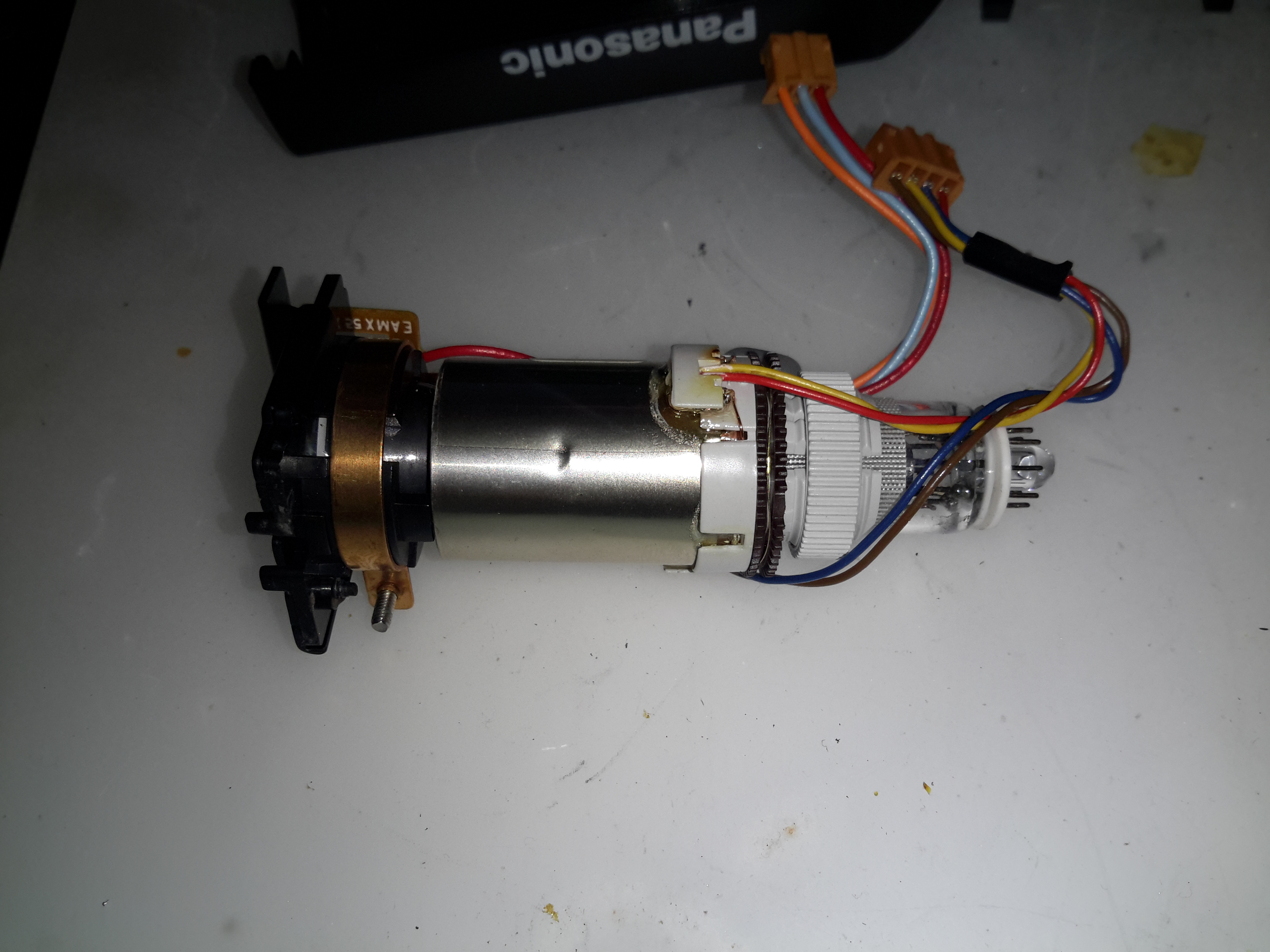
Time foe some more retro tech! This is a 1980’s vintage CCD-based VHS camcorder from Panasonic, the NV-M5. There are a lot of parts to one of these (unlike modern cameras), so I’ll split this post into several sections to make things easier to read (and easier to keep track of what I’m talking about :)).
Left Side
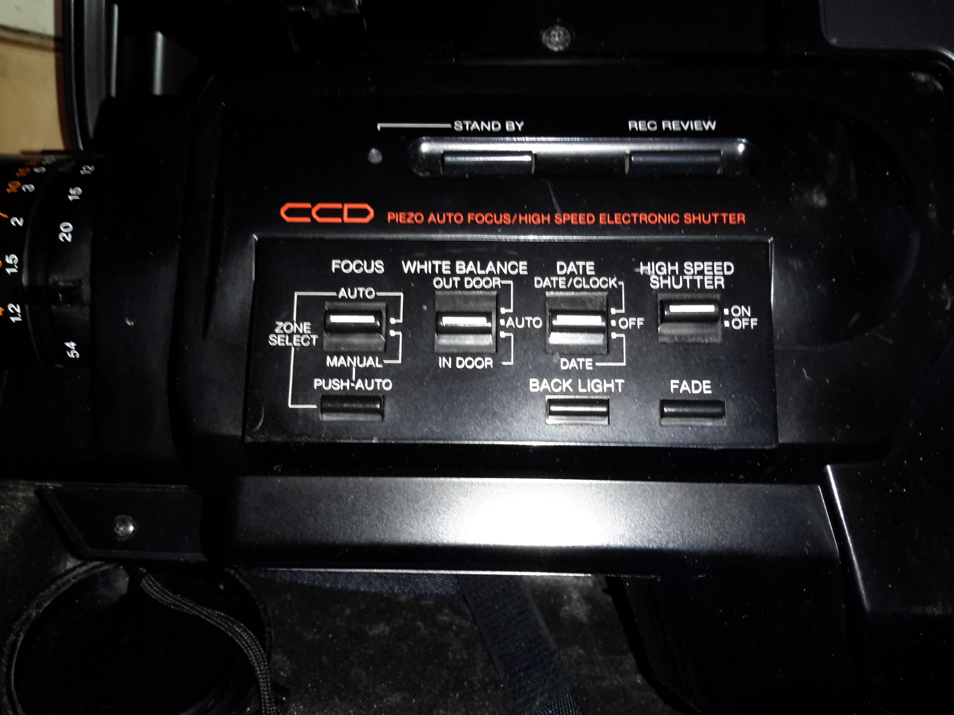
The left side of the camera holds the autofocus, white balance, shutter speed & date controls.
Left Side ControlsLens Adjustments
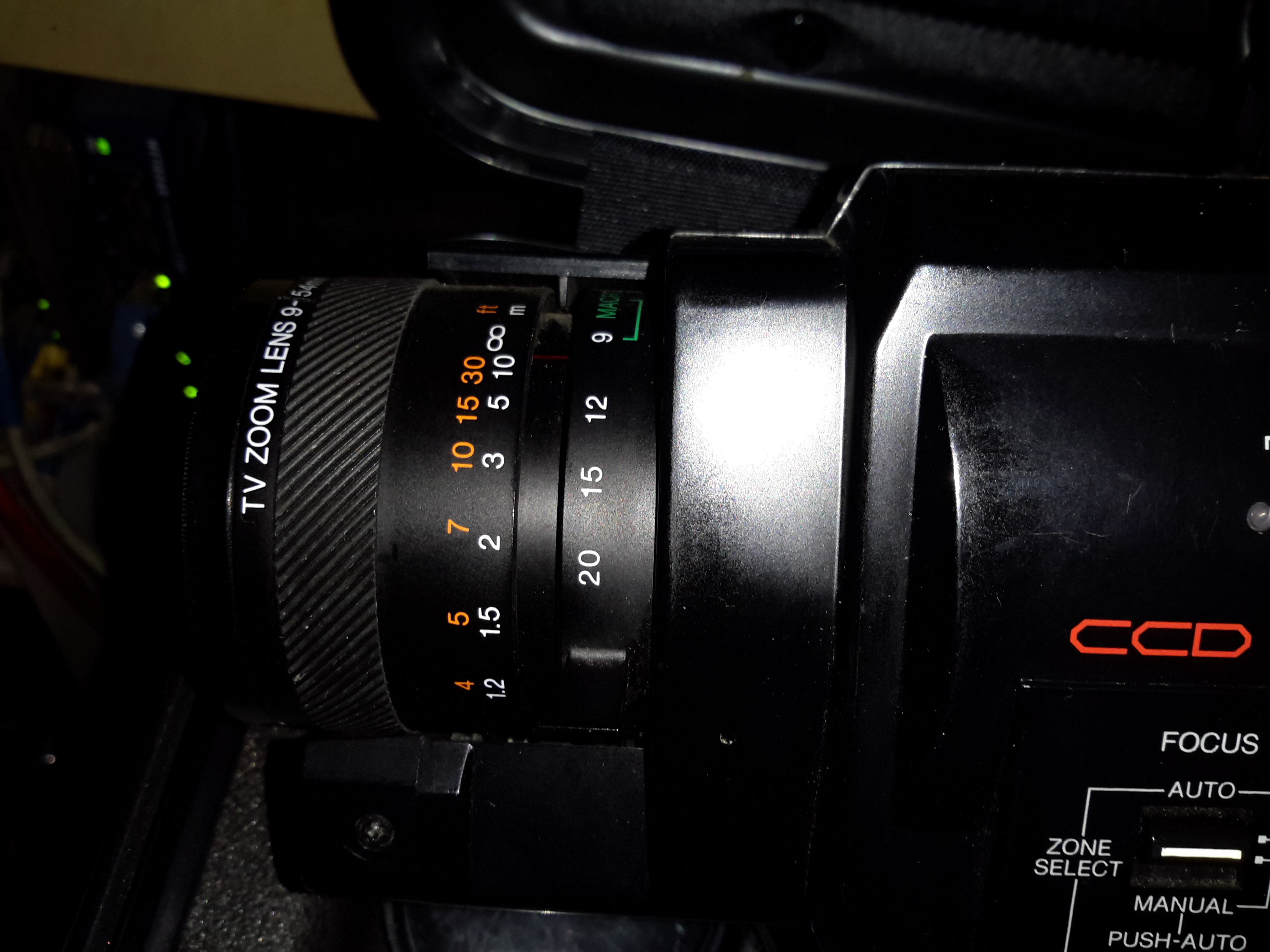
The lens is fully adjustable, with either manual or motorized automatic control.
Rear Panel
The back panel has the battery slot, a very strange looking DC input connector, remote control connector & the earphone jack.
Top Controls
The top panel of the camera holds the main power controls, manual tape tracking & the tape transport control panel.
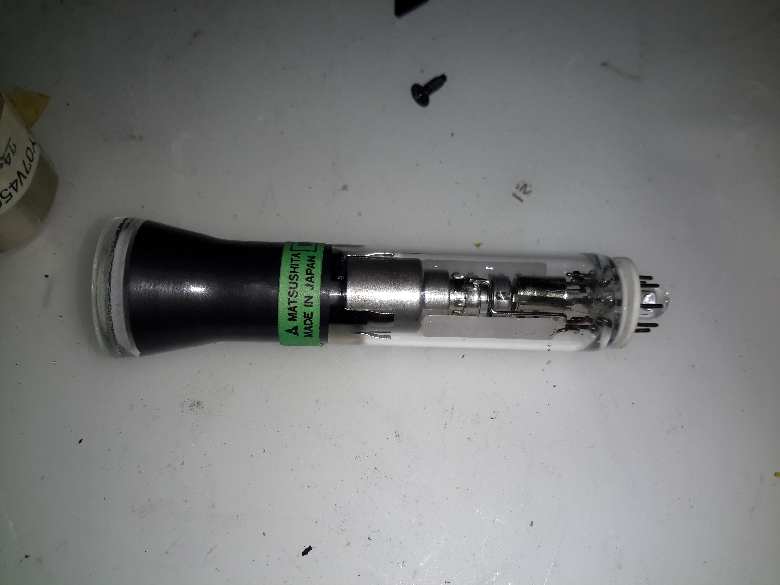
Viewfinder
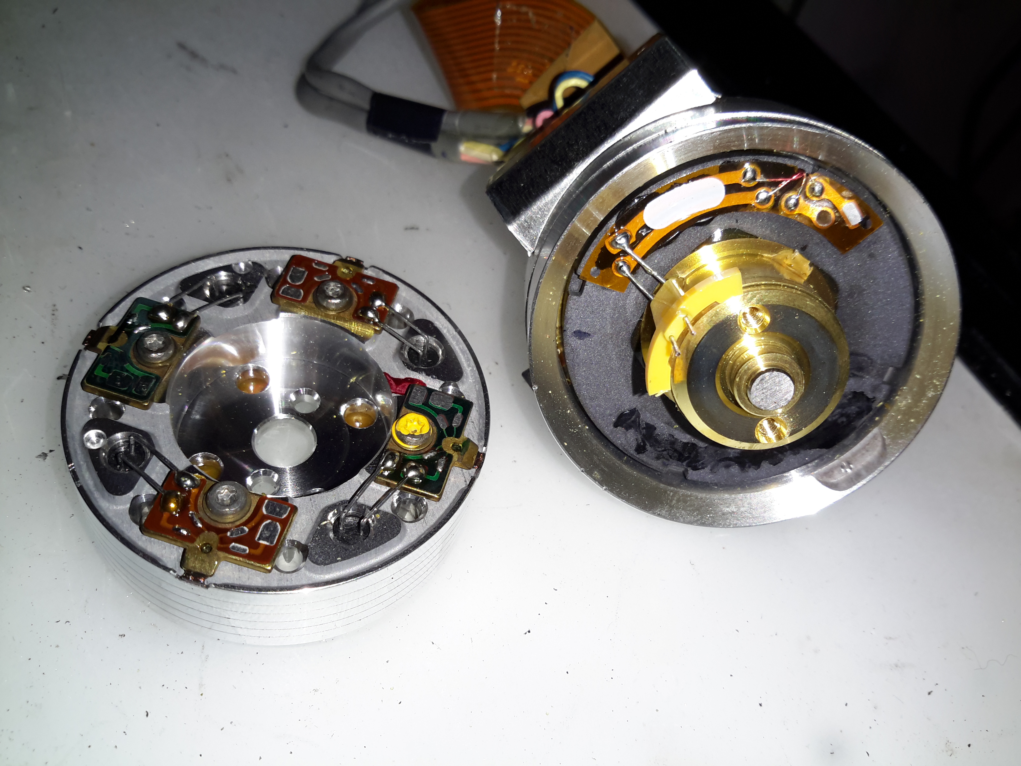
The viewfinder is mounted on a swivel mount. There’s a CRT based composite monitor in here. Hack ahoy!
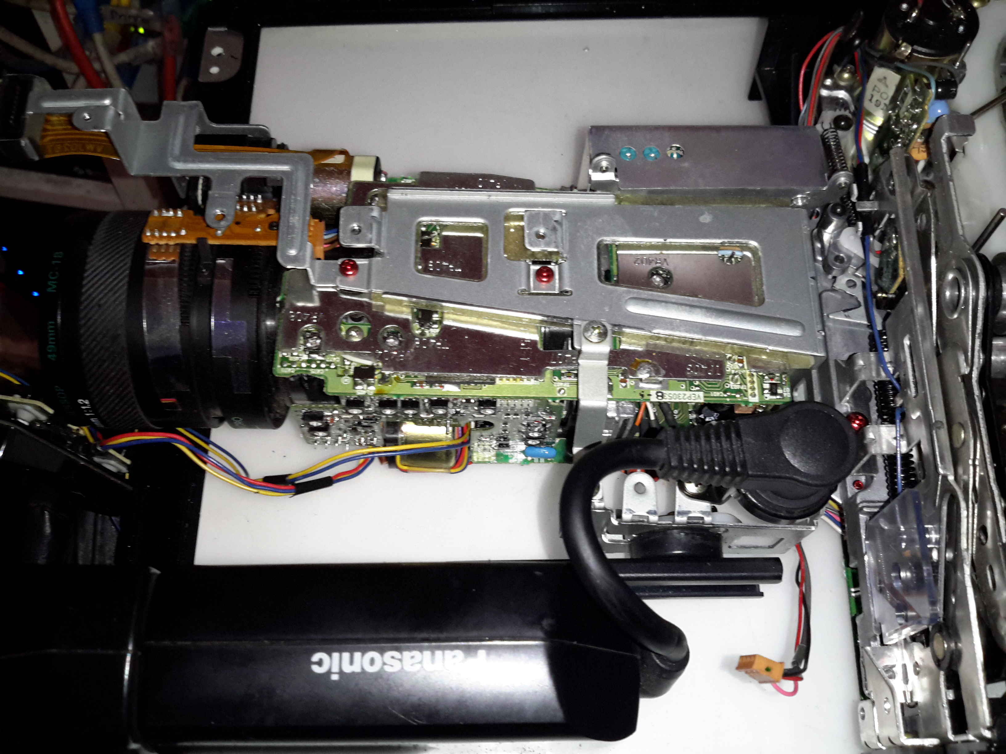
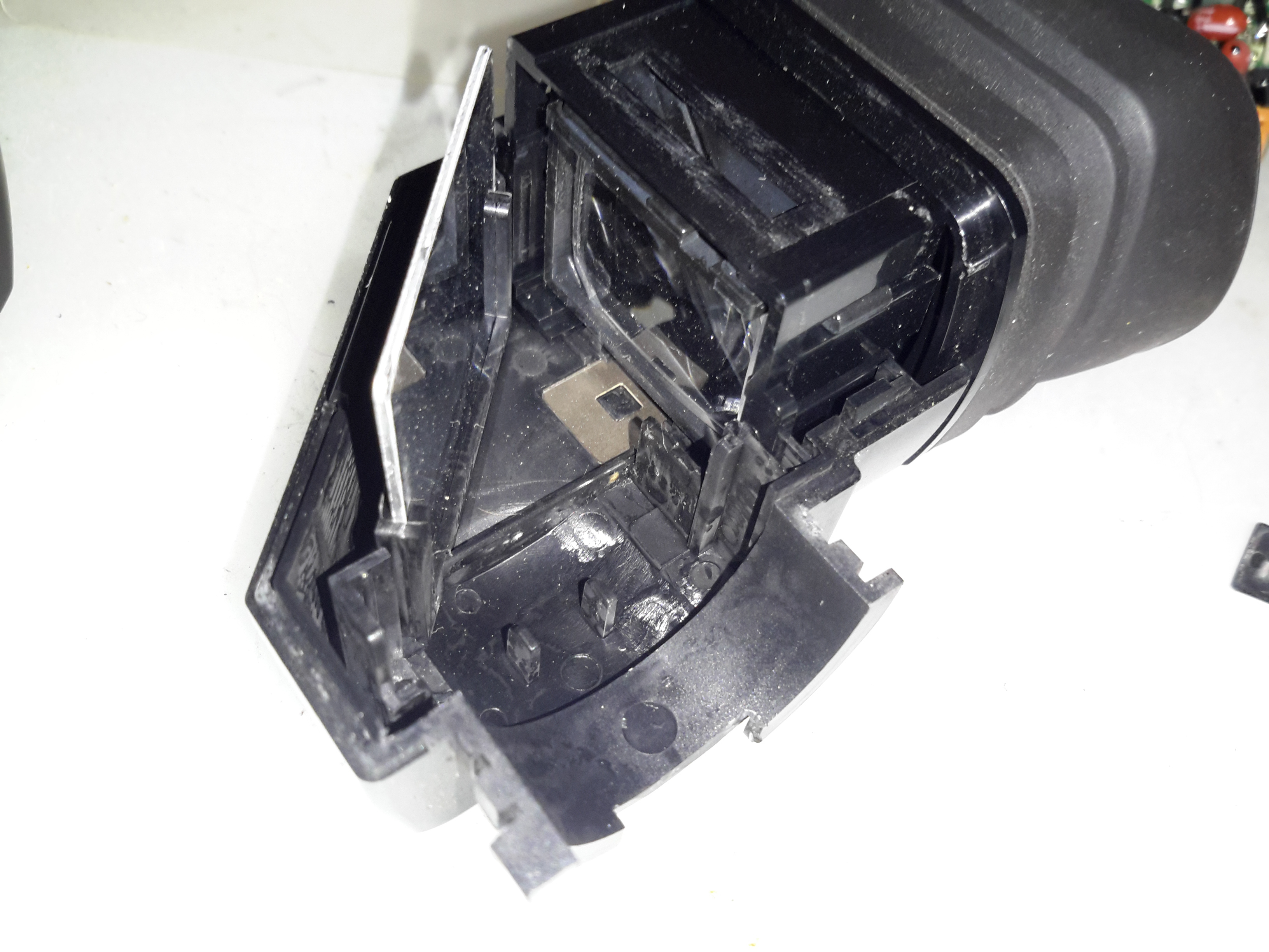
Camera Section
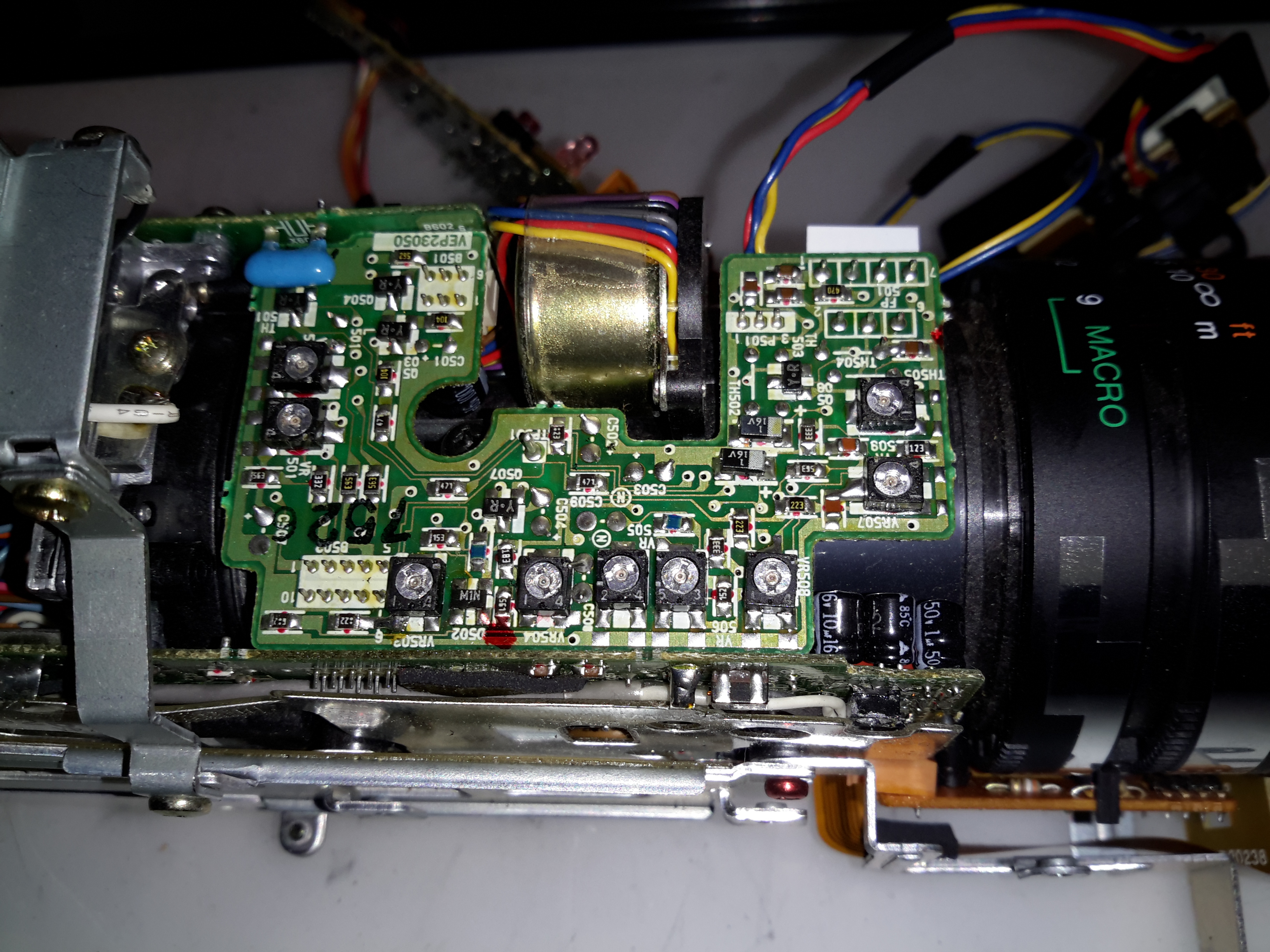
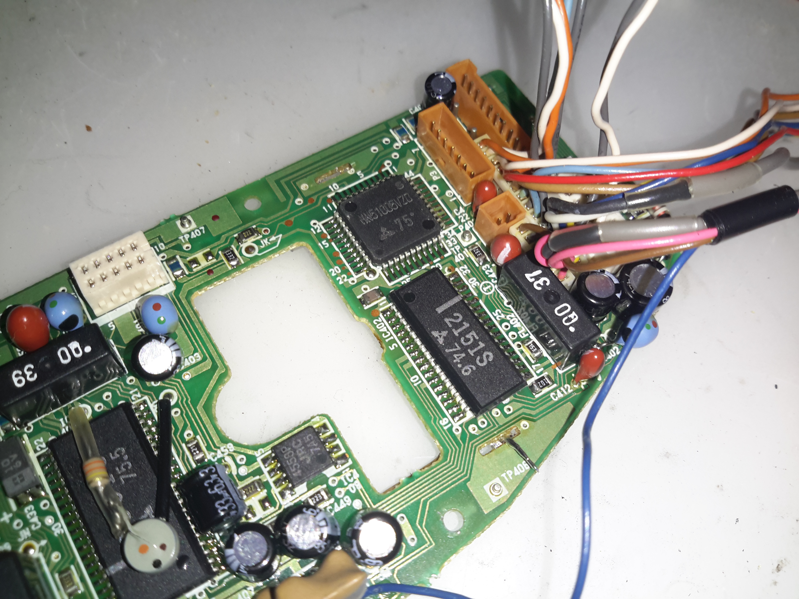
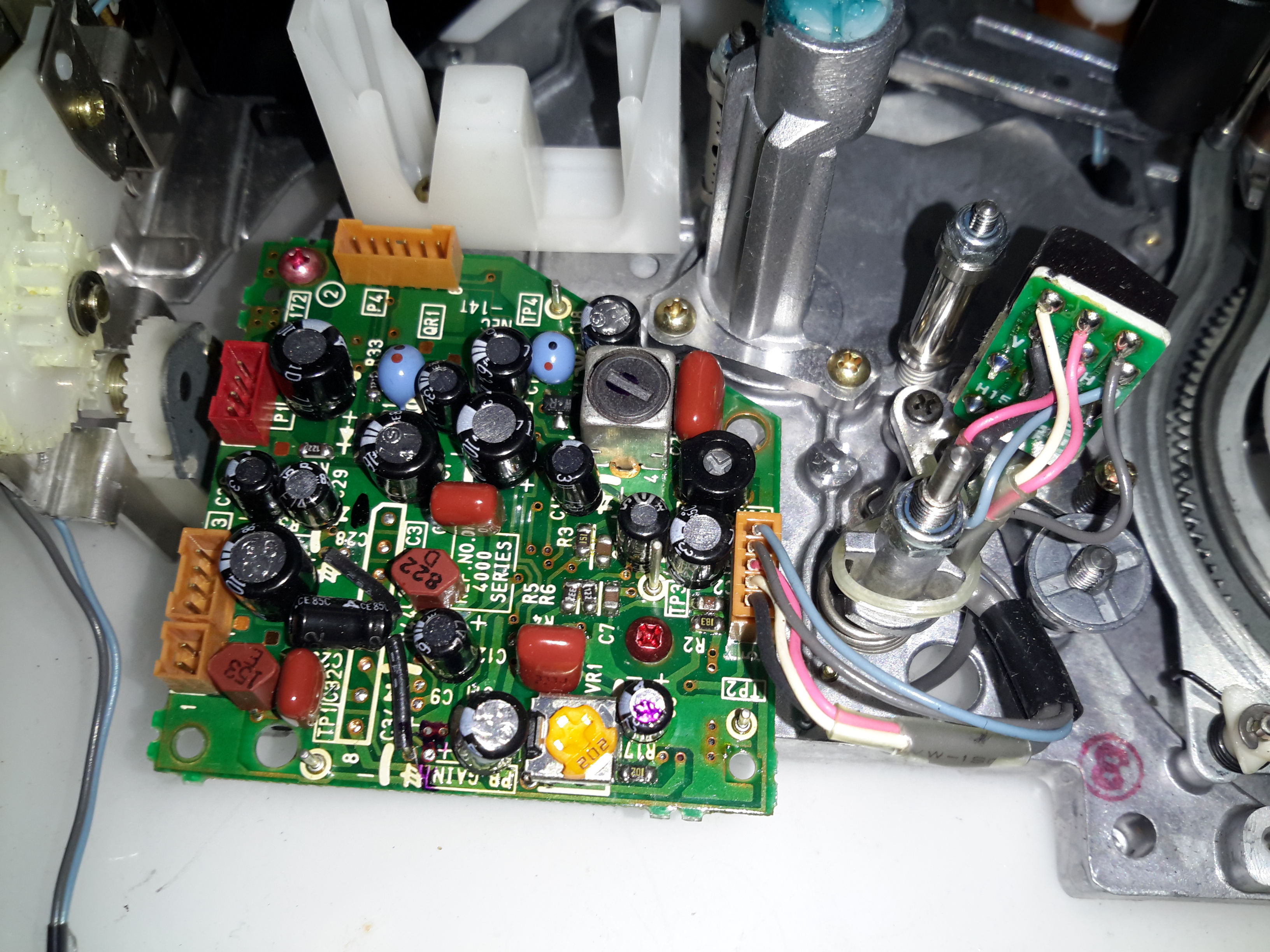
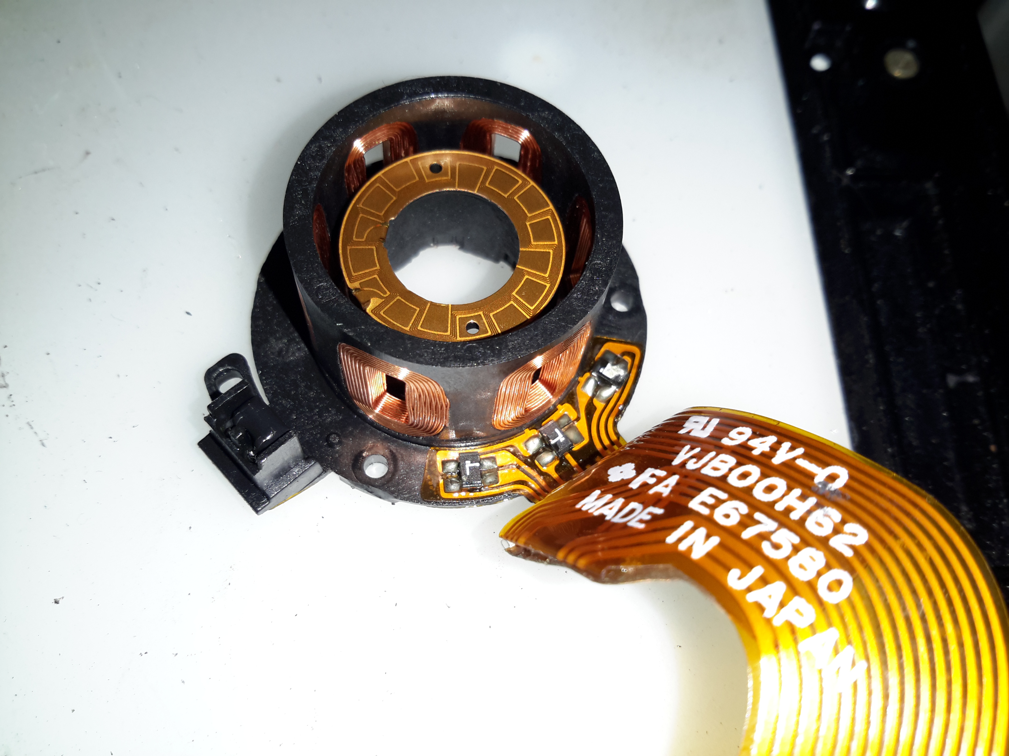
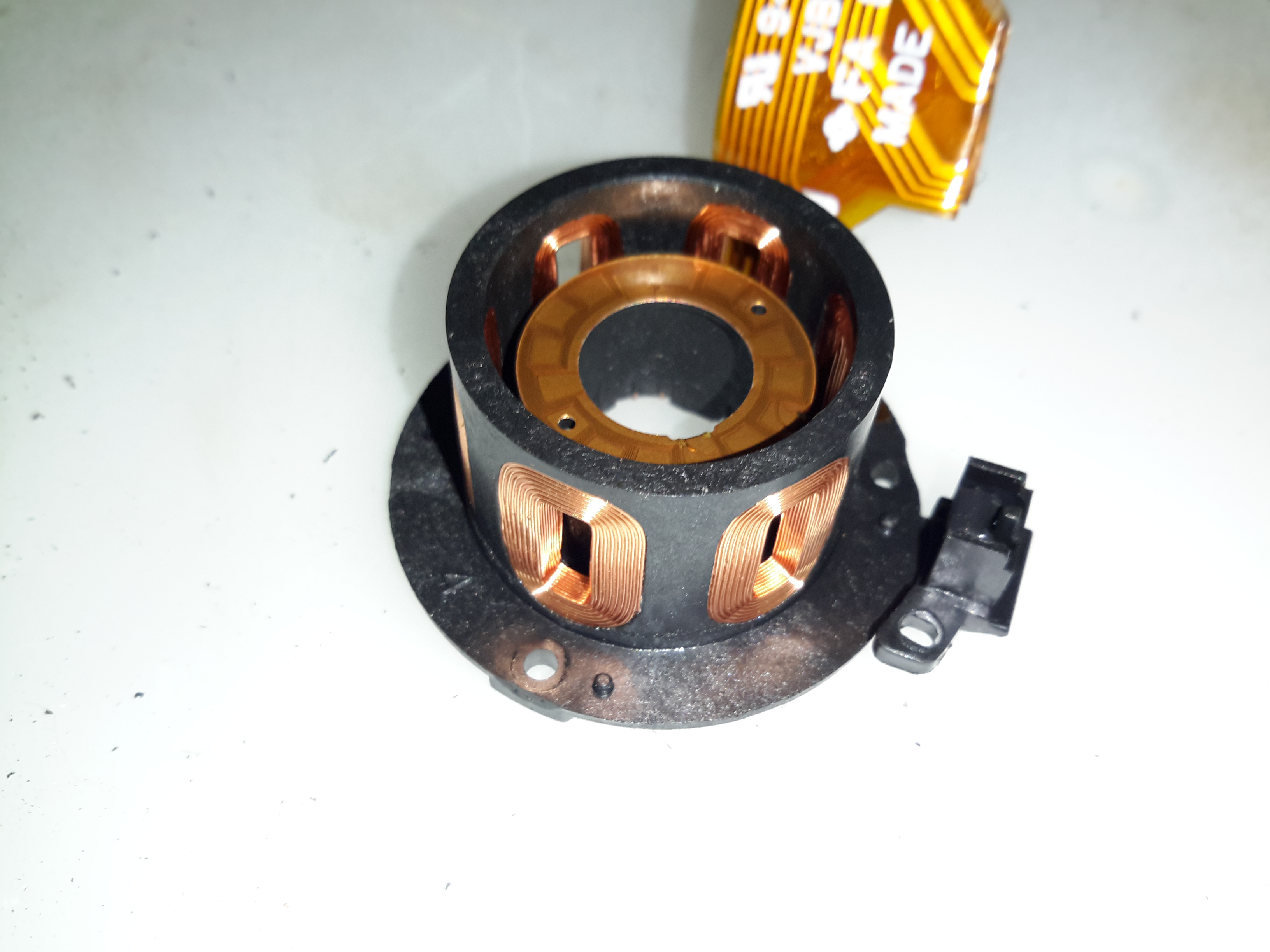
Process Board Assembly
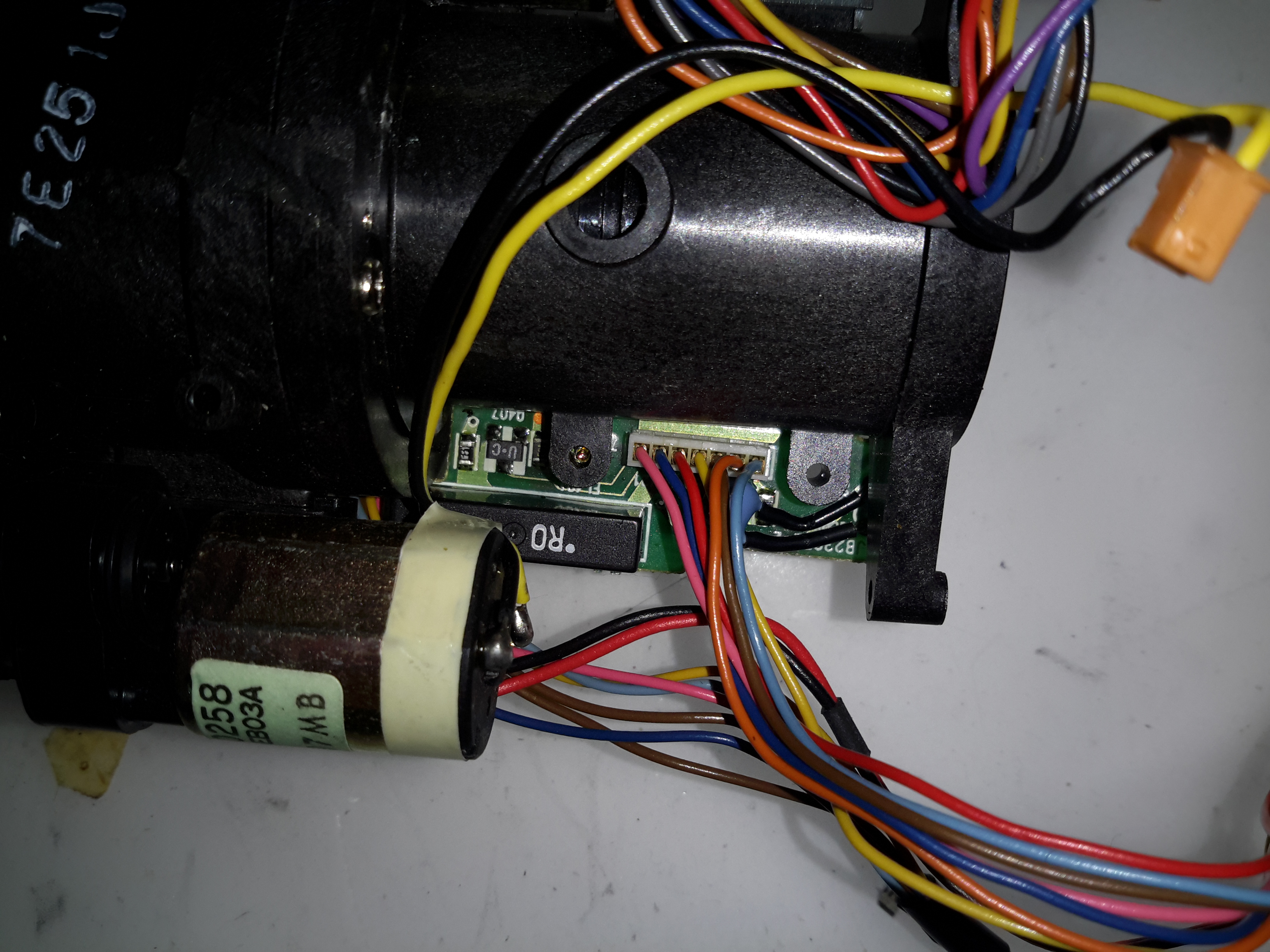
Here’s the camera section of the camcorder, and is totally packed with electronics! There’s at least half a dozen separate boards in here, all fitted together around the optics tube assembly.
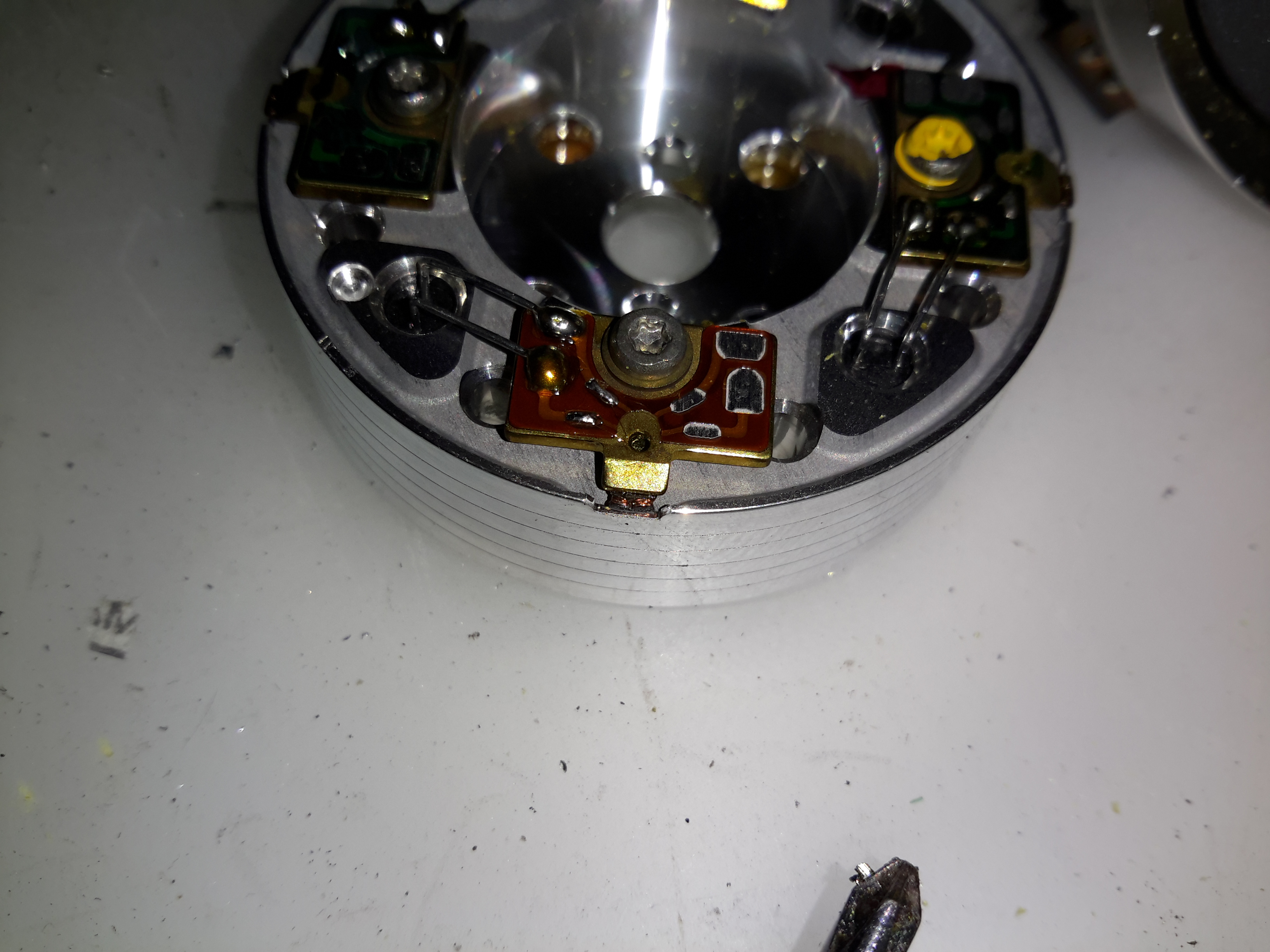
AWB PCB
On the top of the assembly is the Automatic White Balance PCB. Many adjustments here to get everything set right. Not much on the other side of this board other than a bunch of Op-Amps. The iris stepper motor is fitted in a milled opening in the PCB, this connects to one of the other PCBs in the camera module.
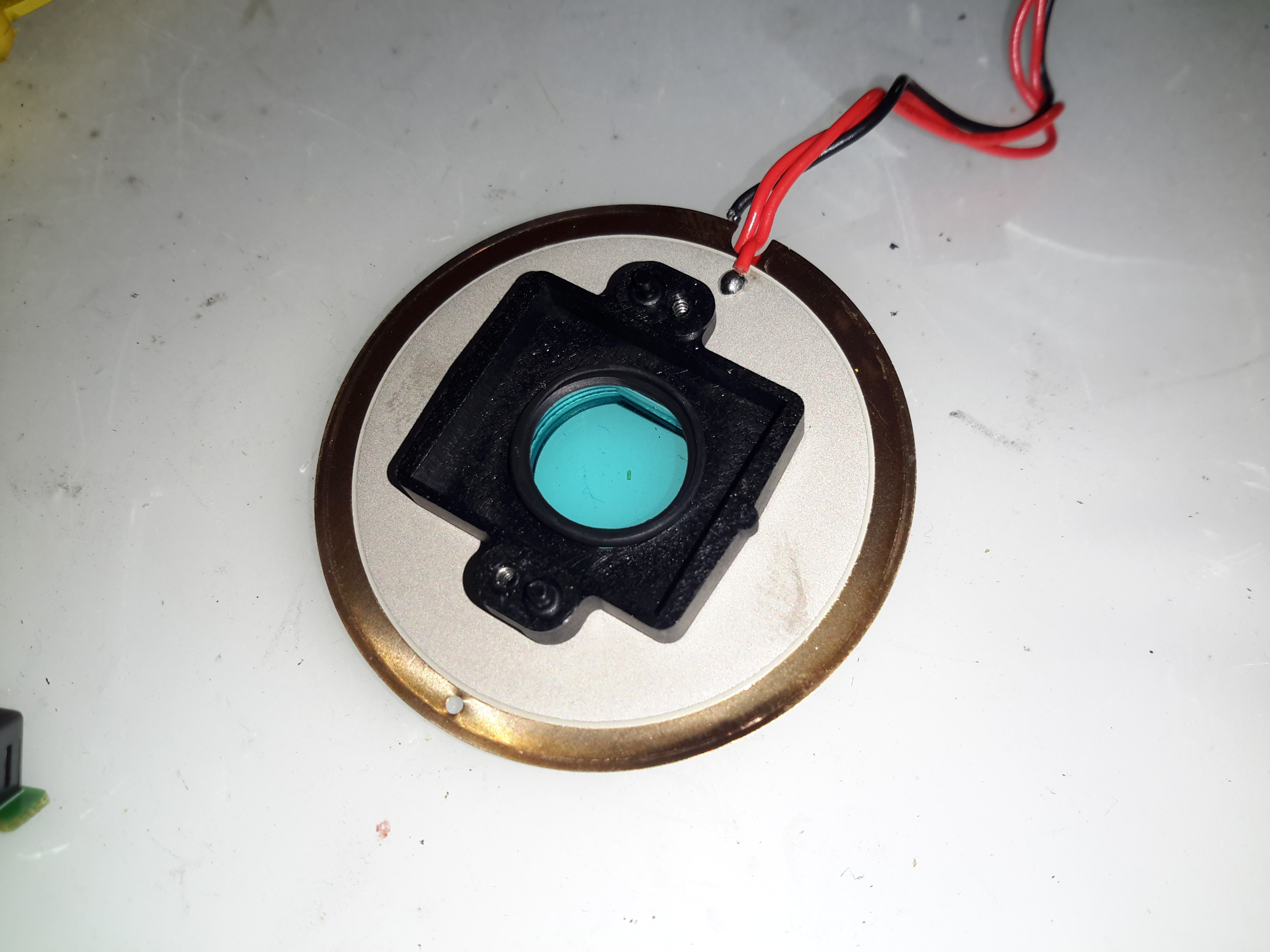
AWB Sensor
Here’s the AWB sensor, mounted next to the lens. I’m not all to certain how this works, but the service manual has the pinout, and there are outputs for all the colour channels, RGB. So it’s probably a trio of photodiodes with filters.
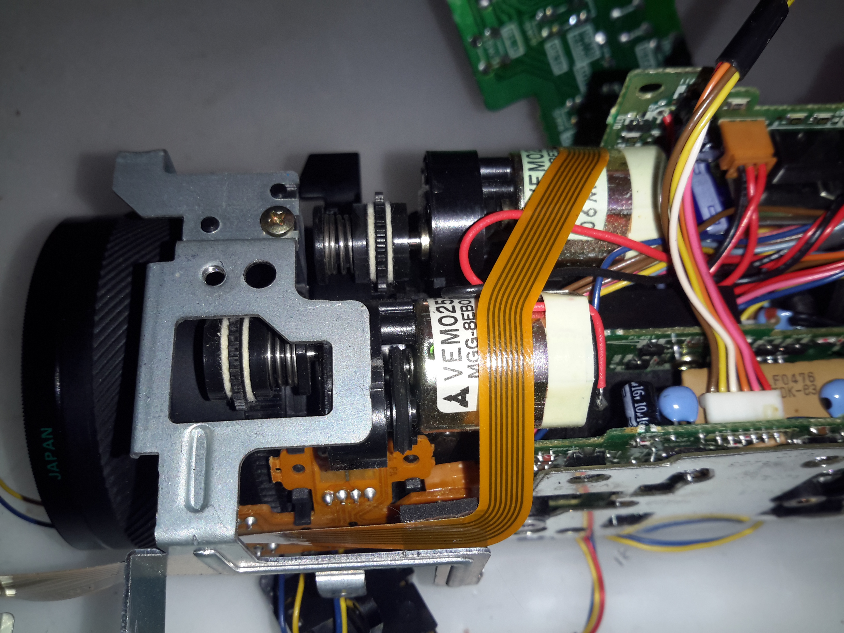
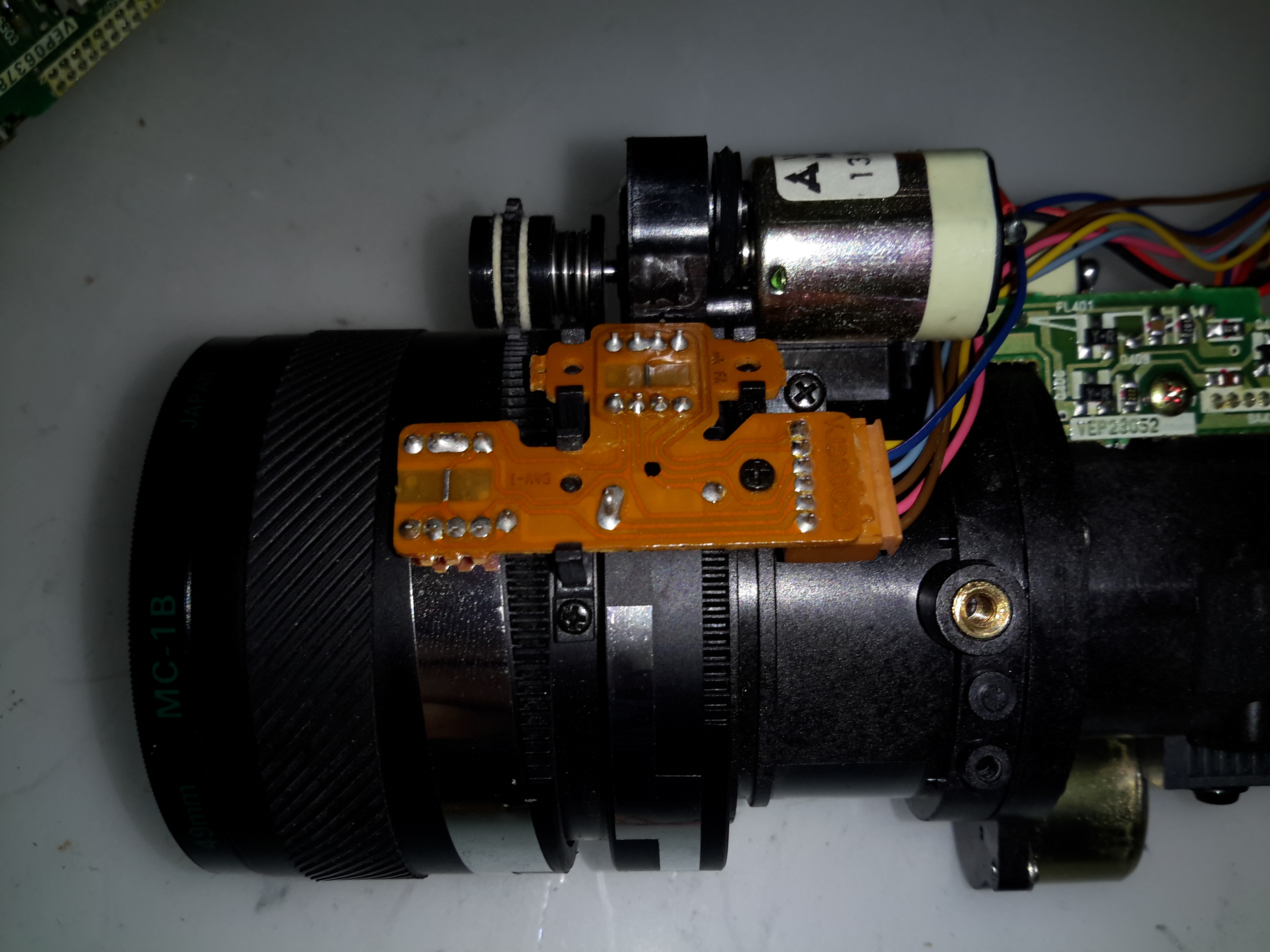
Focus & Zoom Motors
Focus & Zoom are controlled with a pair of DC gear motors. The manual operation is feasible through the use of slip clutches in the final drive pinion onto the lens barrel.
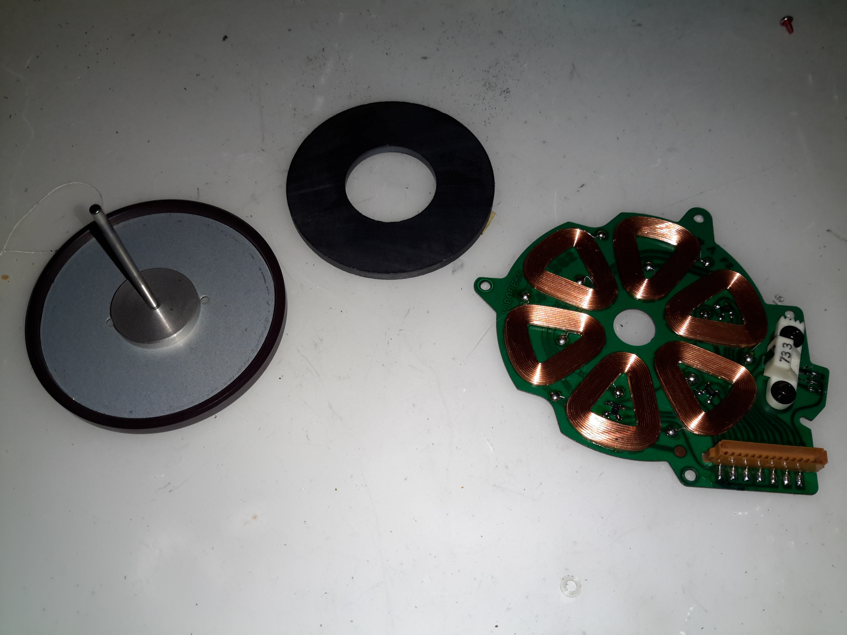
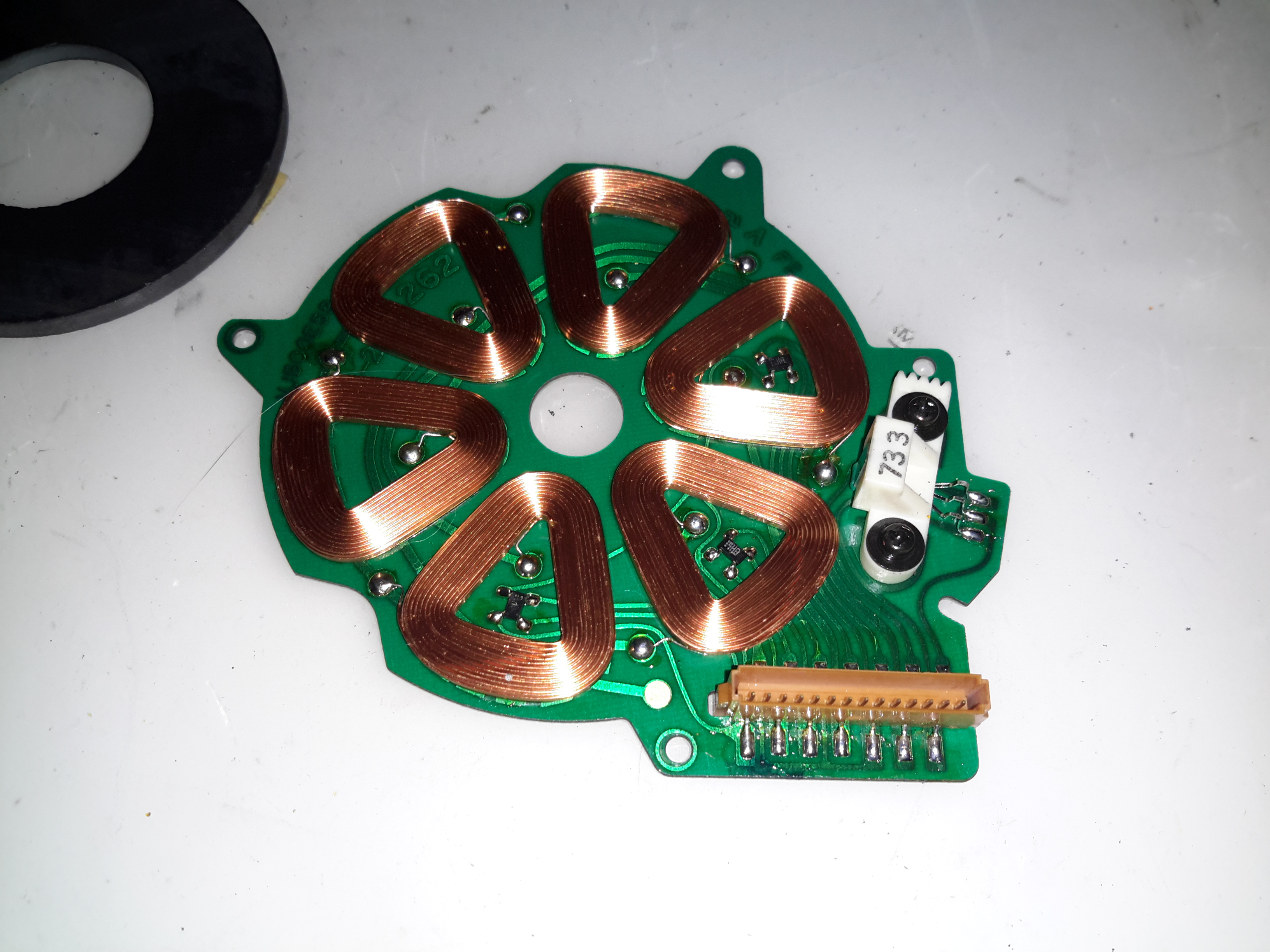
Process Board
The main camera section process board is above. This board does all the signal processing for the CCD, has the bias voltage supplies and houses the control sections for the motorized parts of the optics assembly. There are quite a few dipped Tantalum capacitors on pigtails, instead of being directly board mounted. This was probably done due to space requirements on the PCB itself.
Under the steel shield on this board is some of the main signal processing for the CCD.
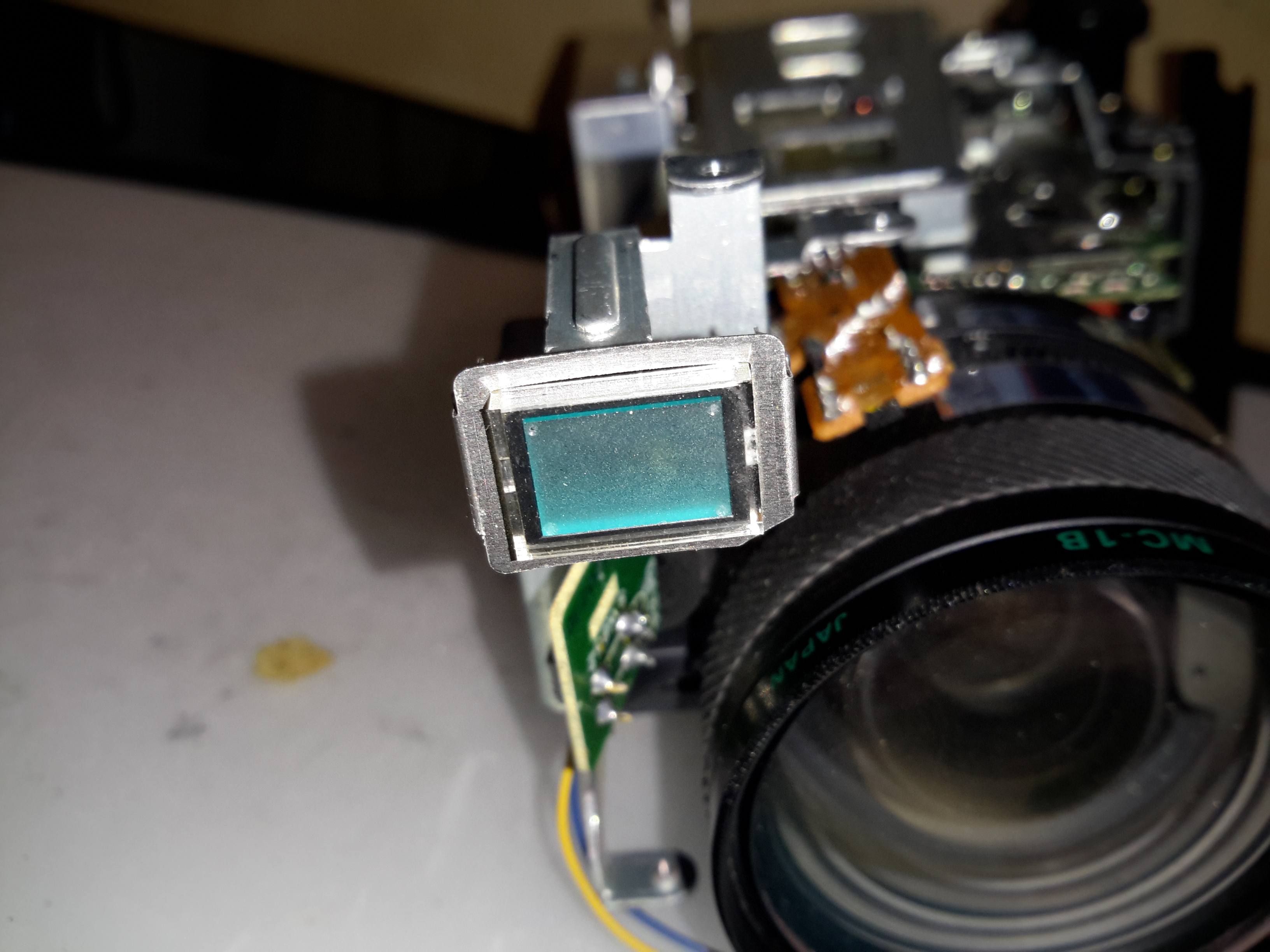
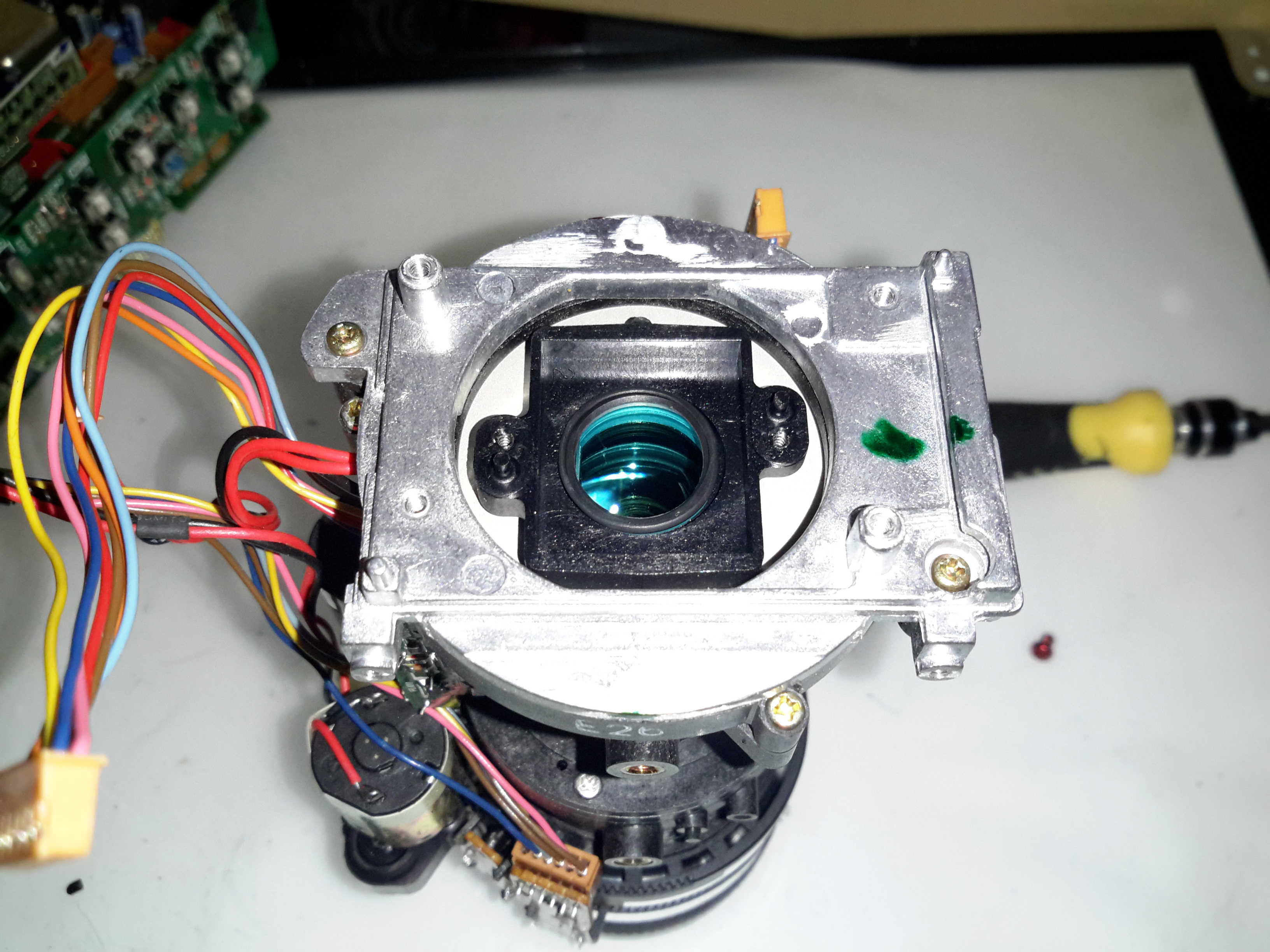
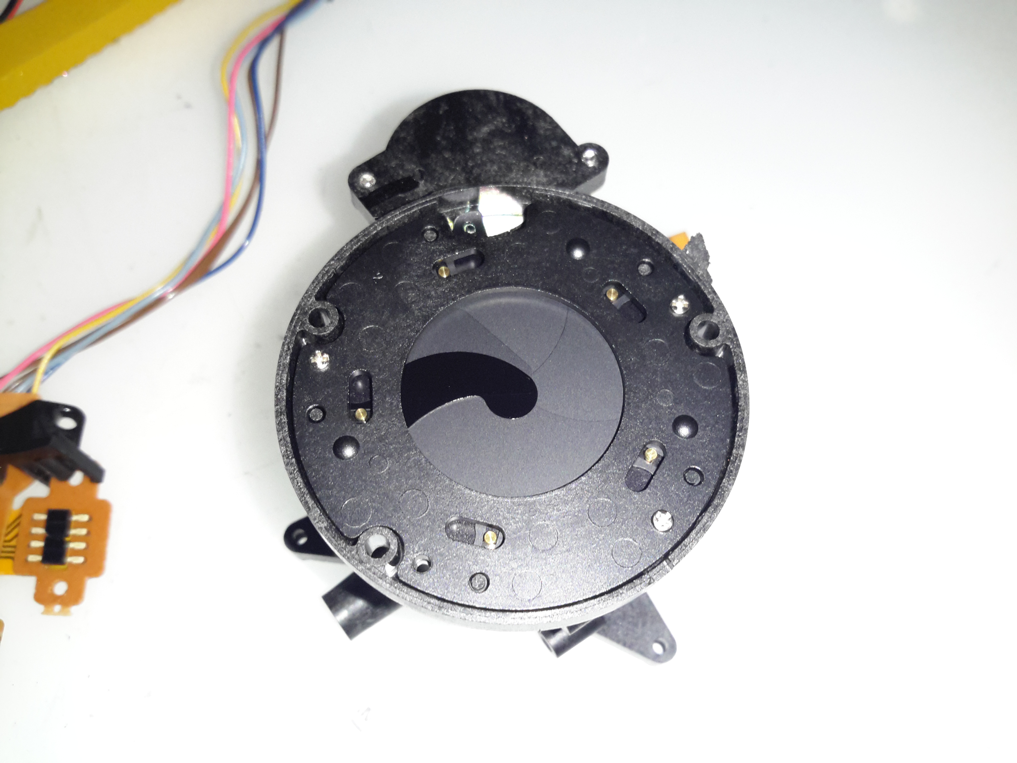
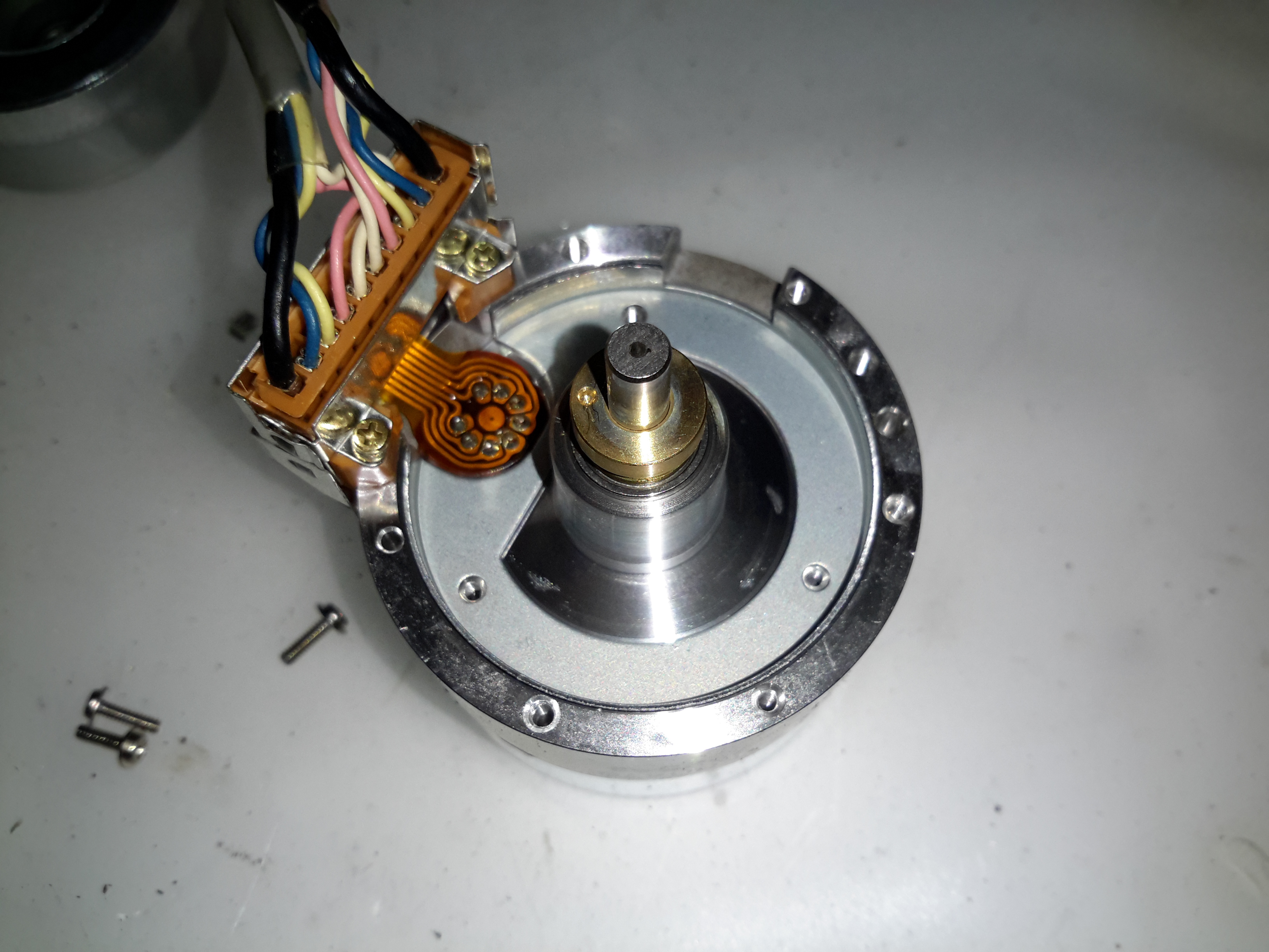
Optics Assembly
The back of the optics tube is a heavy casting, to supress vibration. This will be more clear later on.
Position Sensor Flex
The position of the lens elements is determined by reflective strips on the barrel & sensors on this flex PCB.
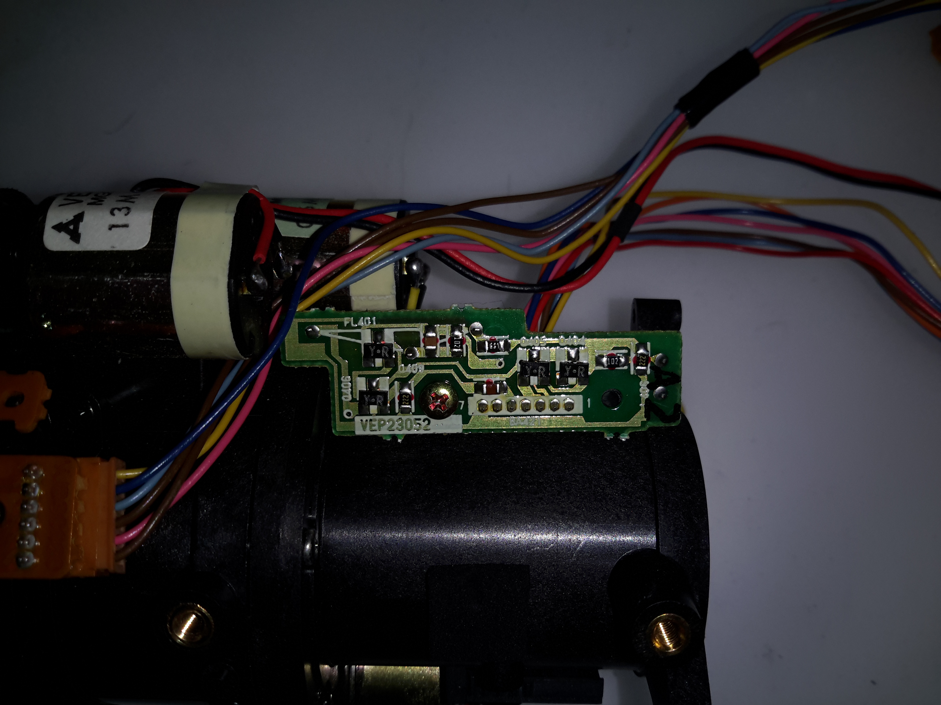
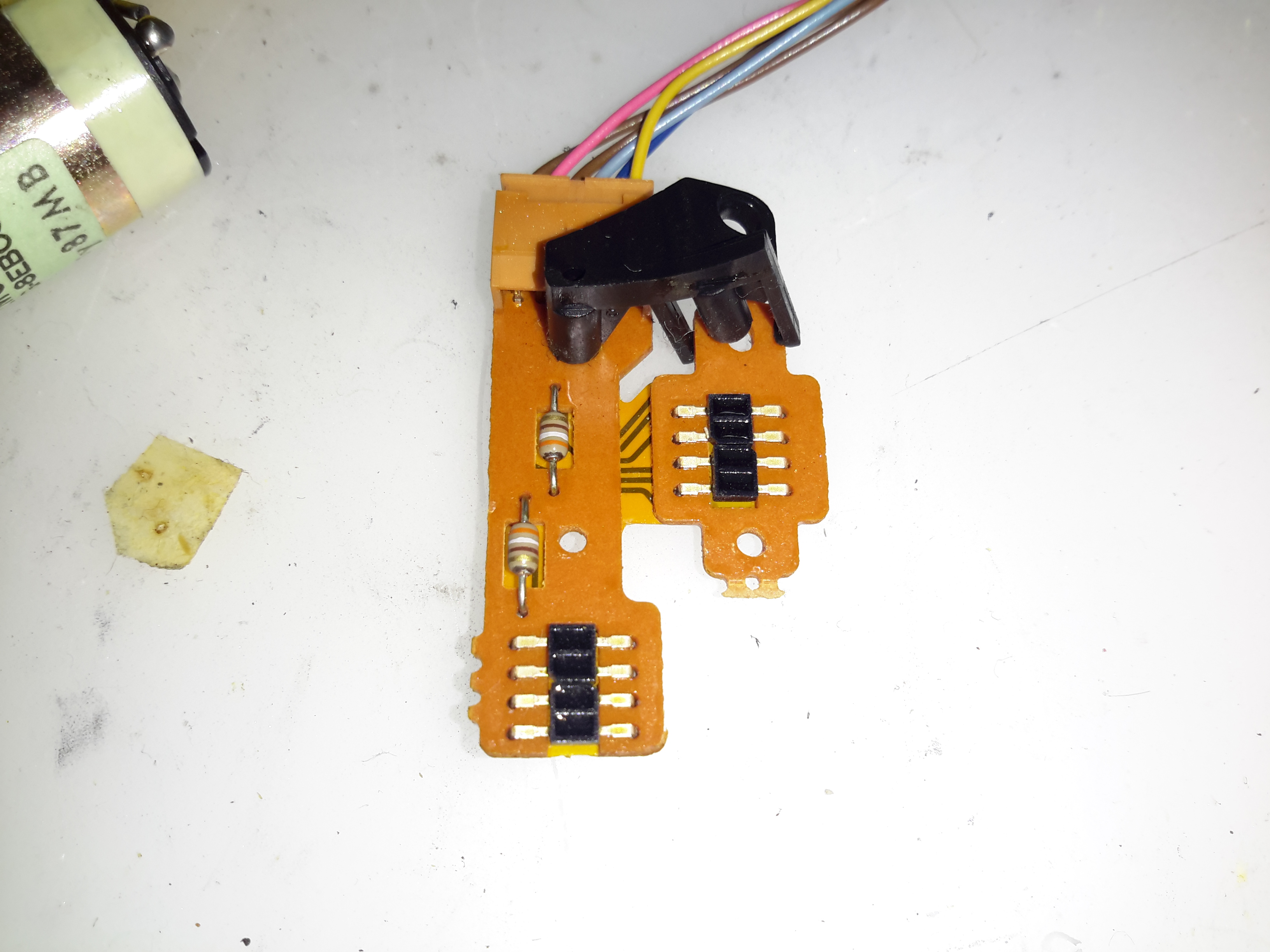
Sub Process Board
There’s another small board tucked into the side of the tube, this hooks into the process PCB.
Process Delay Line
According to the schematic, there’s nothing much on this board, just a delay line & a few transistors.
Piezo Focus Disc
Here’s the reason for the heavy alloy casing at the CCD mounting end of the optics: the fine focus adjustment is done with a piezoelectric disc, the entire CCD assembly is mounted to this board. Applying voltage to the electrodes moves the assembly slightly to alter the position of the CCD. The blue glass in the centre of the unit is the IR filter.
IR Relective Sensors
The barrel position sensors are these IR-reflective type.
Iris Assembly
The iris is mounted just before the CCD, this is controlled with a galvanometer-type device with position sensors incorporated.
Iris Opening
Pushing on the operating lever with the end of my screwdriver opens the leaves of the iris against the return spring.
Tape Transport & Main Control
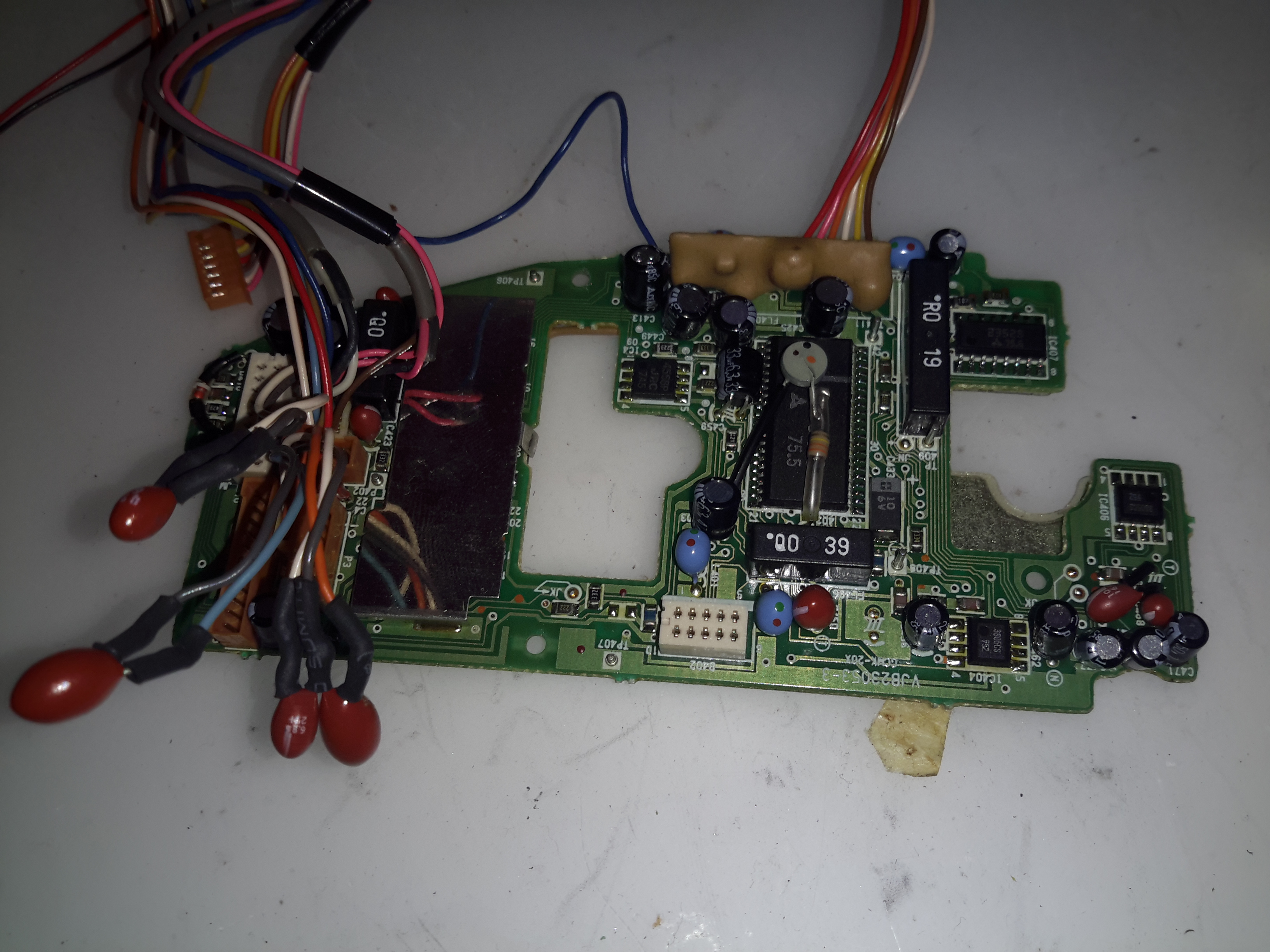
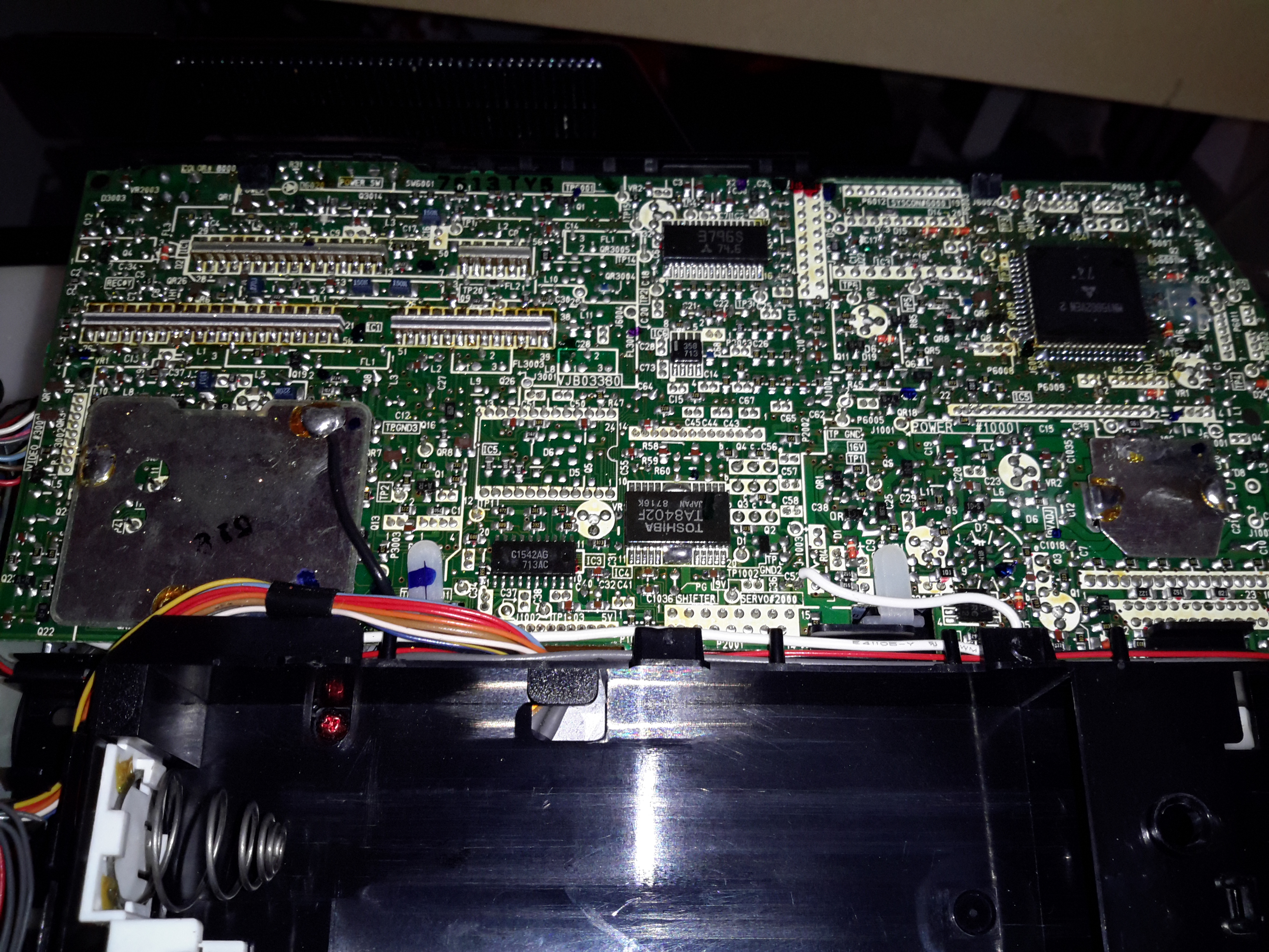
Main Control Board
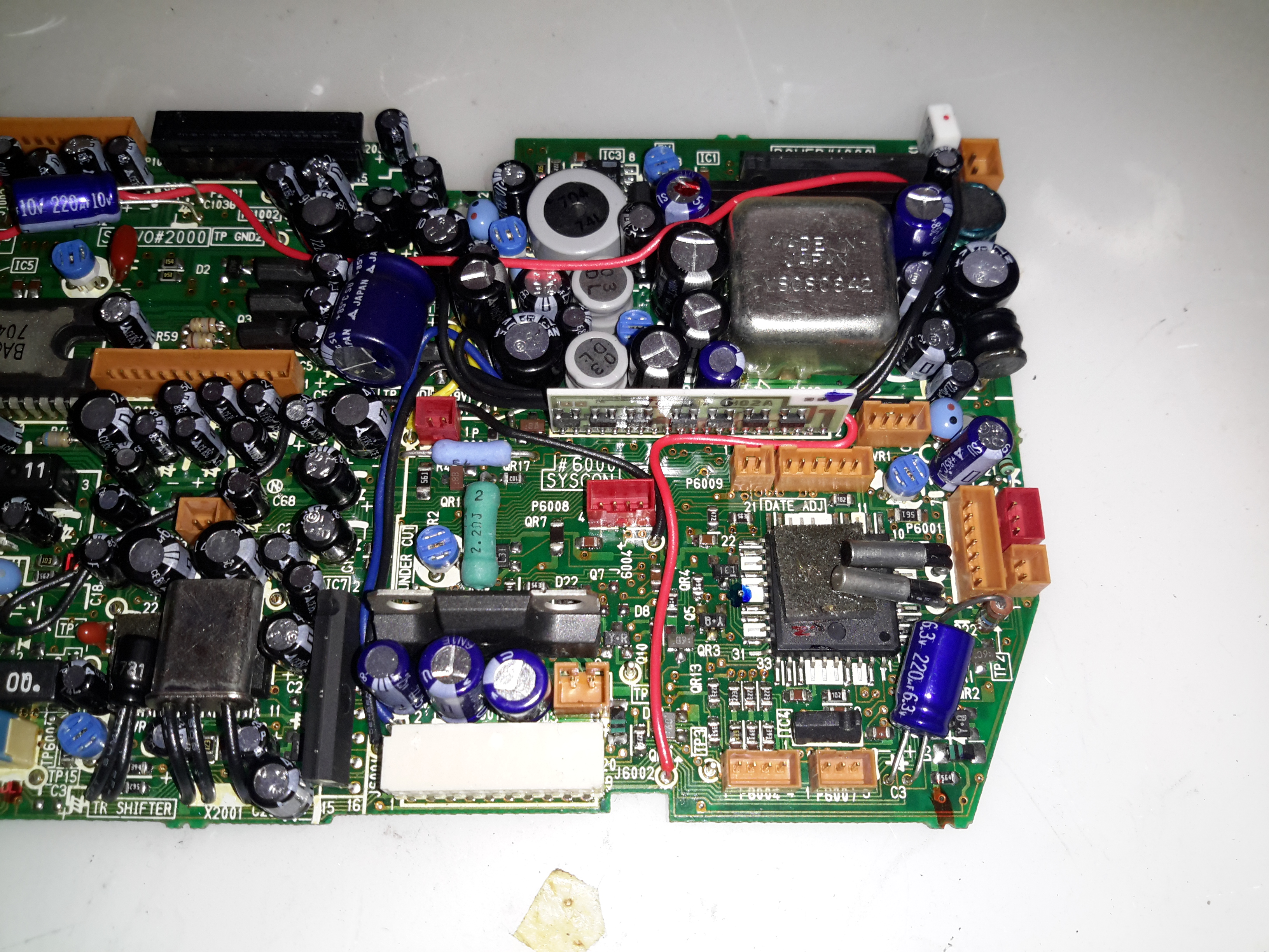
Tucked into the side of the main body of the unit is the main system control board. This PCB houses all the vital functions of the camera: Power Supply, Servo Control, Colour Control,Video Amplifiers, etc.
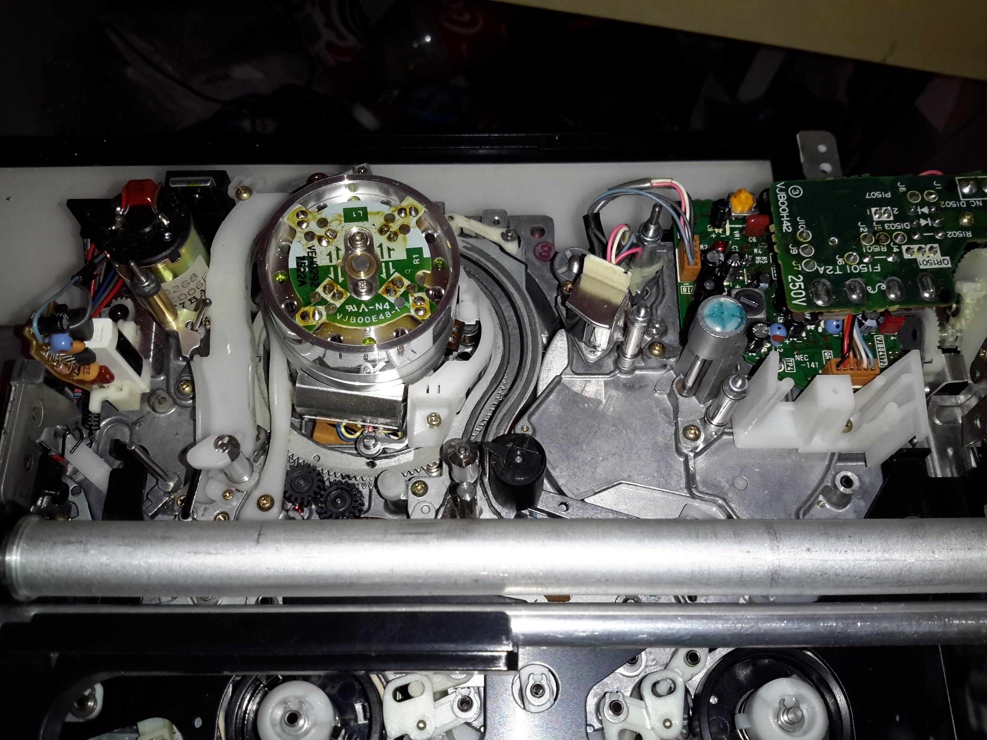
Tape Drum
Here’s the main tape transport mechanism, this is made of steel & aluminium stampings for structural support. The drum used in this transport is noticeably smaller than a standard VHS drum, the tape is wrapped around more of the drum surface to compensate.
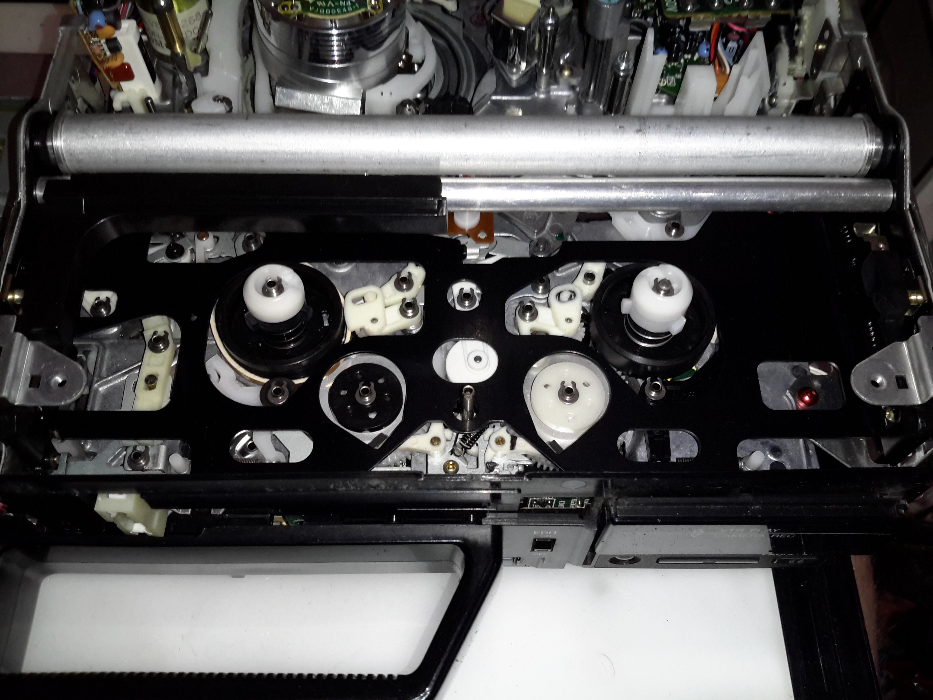
Tape Transport
The VHS tape sits in this carriage & the spools drive the supply & take up reels in the cartridge.
Main Control PCB
Here’s the component side of the main control PCB. This one is very densely packed with parts, I wouldn’t like to try & troubleshoot something like this!
Main PCB Left
The left side has the video head amp at the top, a Panasonic AN3311K 4-head video amp. Below that is video processing, the blue components are the analogue delay lines. There are a couple of hybrid flat-flex PCBs tucked in between with a couple of ICs & many passives. These hybrids handle the luma & chroma signals.
Top left is the capstan motor driver a Rohm BA6430S. The transport motors are all 3-phase brushless, with exception of the loading motor, which is a brushed DC type.
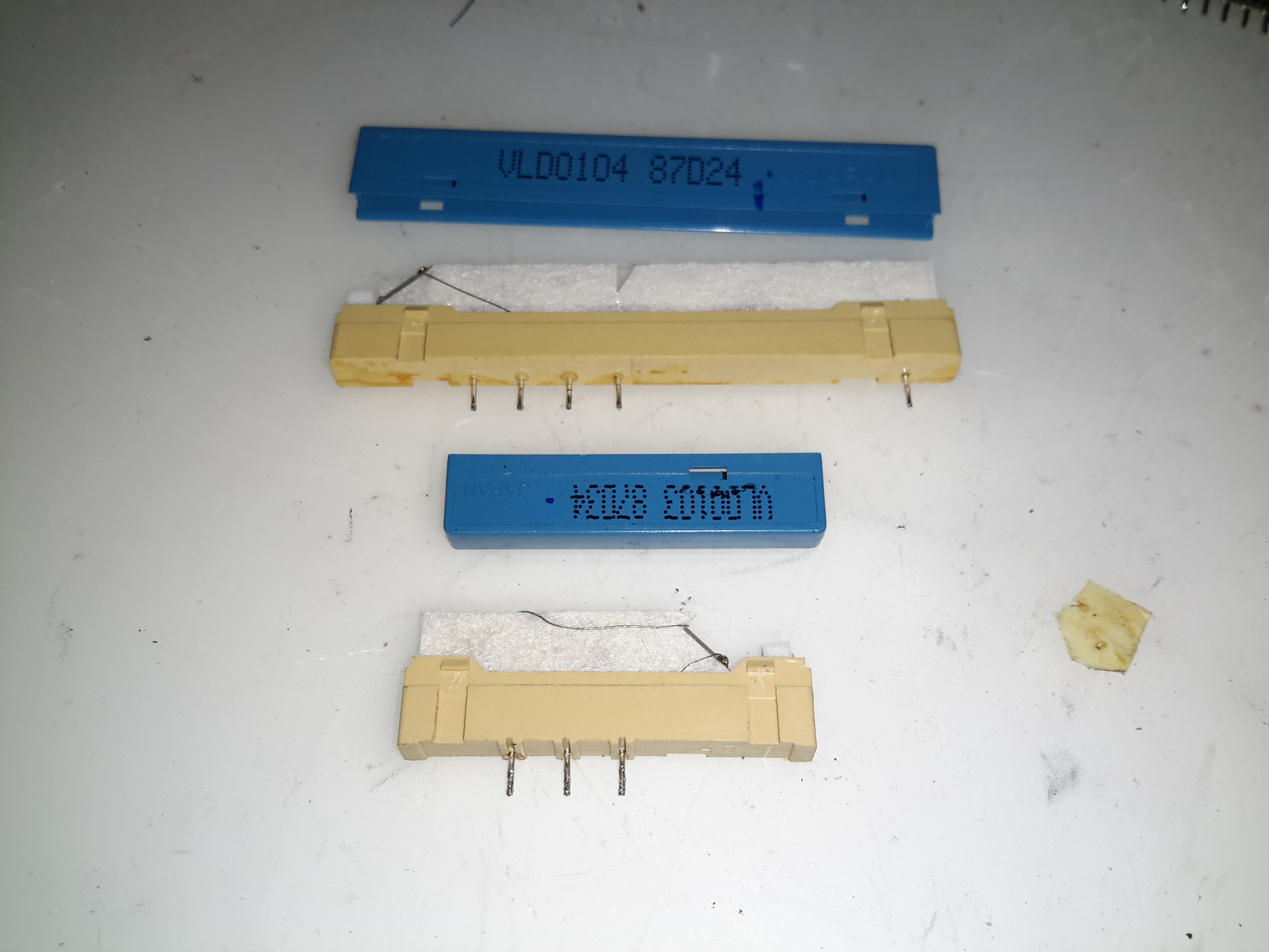
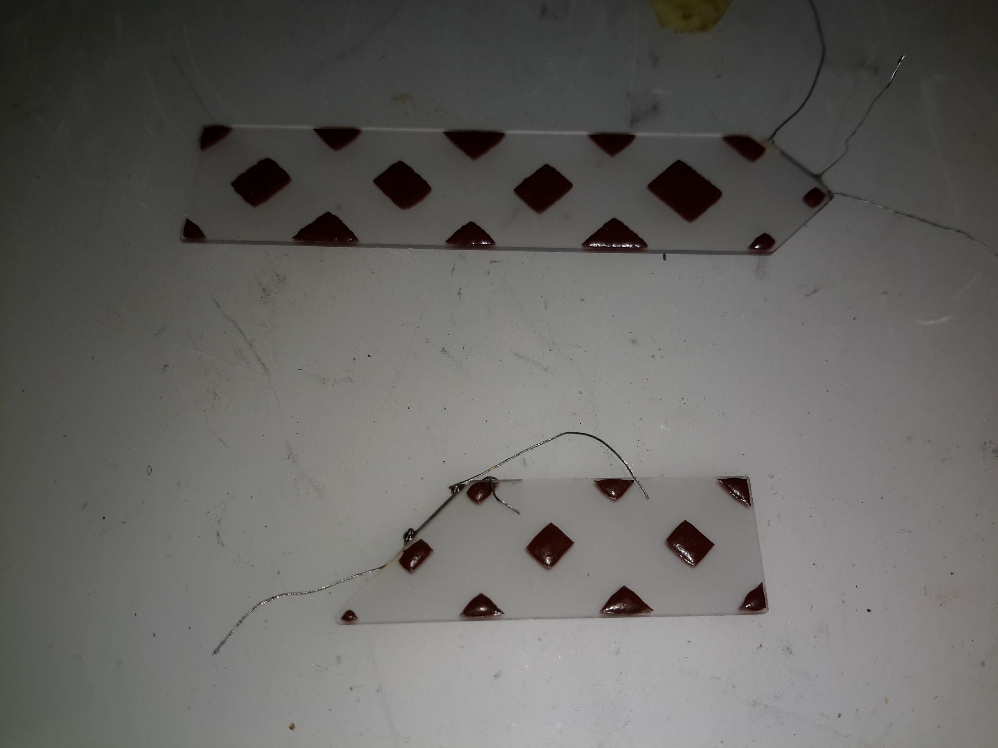
Delay Line
Here’s what is inside the delay lines for the analogue video circuits. The plastic casing holds a felt liner, inside which is the delay line itself.
Internal Glass
The delay is created by sending an acoustic signal through the quartz crystal inside the device by a piezoelectric transducer, bouncing it off the walls of the crystal before returning it to a similar transducer.
Main PCB Centre
Here’s the centre of the board, the strange crystal at bottom centre is the clock crystal for the head drum servo. Why it has 3 pins I’m not sure, only the two pins to the crystal inside are shown connected on the schematic. Maybe grounding the case?
The main servo controls for the head drum & the capstan motor are top centre, these get a control signal from the tape to lock the speed of the relative components.
Main PCB Right
Here’s the right hand side. The main power supply circuitry is at top right, with a large can containing 4 switching inductors & a ferrite pot core transformer. All these converters are controlled by a single BA6149 6-channel DC-DC converter controller IC via a ULN2003 transistor array.
The ceramic hybrid board next to the PSU has 7 switch transistors for driving various indicator LEDs.
The large tabbed IC bottom centre is the loading motor drive, an IC from Mitsubishi, the M54543. This has bidirectional DC control of the motor & built in braking functions. The large quad flat pack IC on the right is the MN1237A on-screen character generator, with the two clock crystals for the main microcontroller.
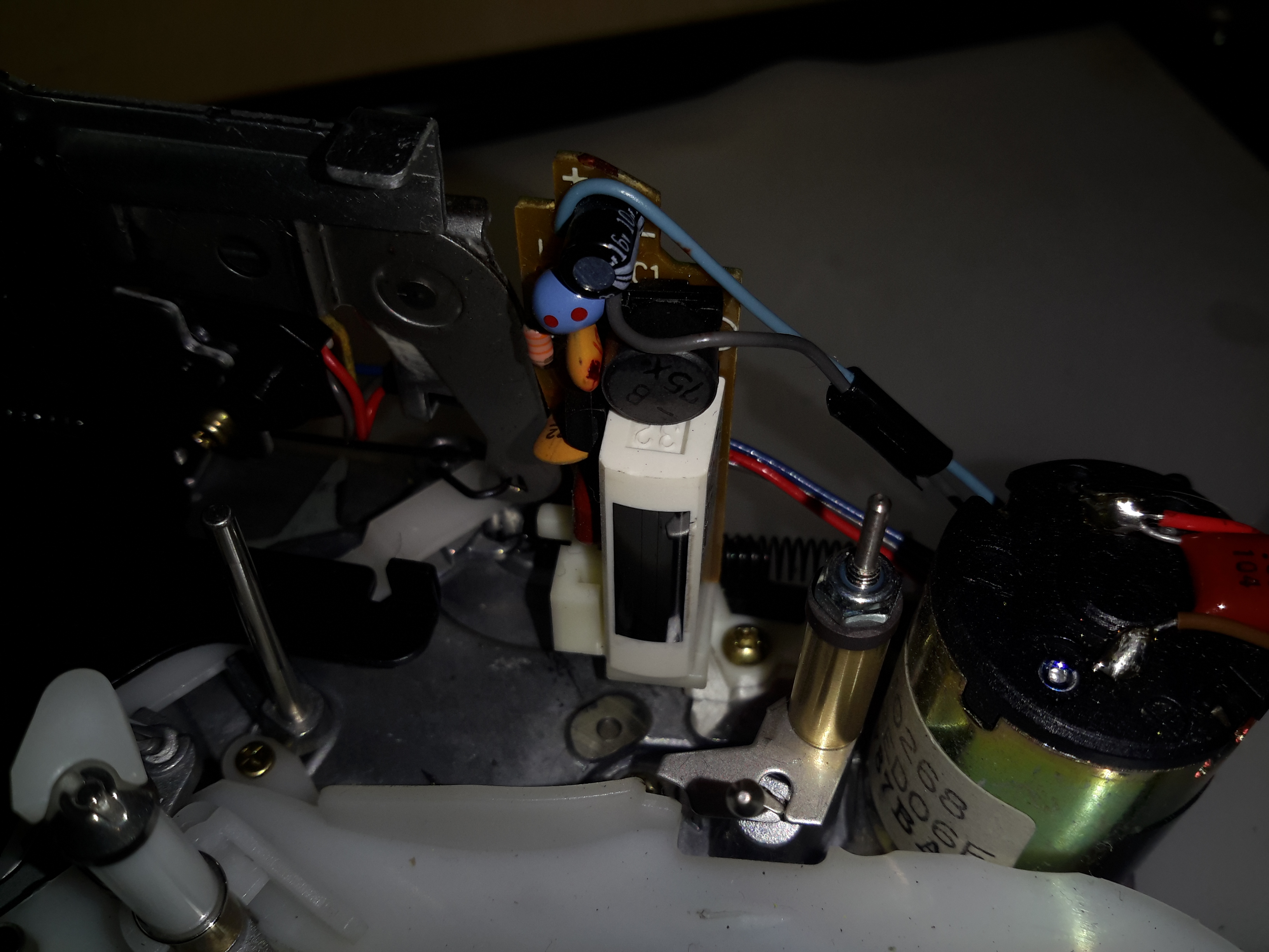
Erase Head
The full erase head has it’s power supply & oscillator on board, applying 9v to this board results in an AC signal to the head, which erases the old recording from the tape before the new recording is laid down by the flying heads on the drum.
Audio Control PCB
The Audio & Control head is connected to this PCB, which handles both reading back audio from the tape & recording new audio tracks. The audio bias oscillator is on this board, & the onboard microphone feeds it’s signal here. The control head is fed directly through to the servo section of the main board.
Drum Motor
The motor that drives the head drum is another DC brushless 3-phase type.
Hall Sensors
These 3 Hall sensors are used by the motor drive to determine the rotor position & time commutation accordingly.
Stator
The stator on this motor is of interesting construction, with no laminated core, the coils are moulded into the plastic holder. The tach sensor is on the side of the stator core. This senses a small magnet on the outside of the rotor to determine rotational speed. For PAL recordings, the drum rotates at 1500 RPM.
Motor Removed
Not much under the stator other than the bearing housing & the feedthrough to the rotary transformer.
Head Disc
The heads are mounted onto the top disc of the drum, 4 heads in this recorder. The signals are transmitted to the rotating section through the ferrite rotary transformer on the bottom section.
Head Chip
The tiny winding of the ferrite video head can just about be seen on the end of the brass mounting.
Capstan Motor Components
The capstan motor is similar to the drum motor, only this one is flat. The rotor has a ferrite magnet, in this case it wasn’t glued in place, just held by it’s magnetic field.
Capstan Motor Stator
The PCB on this motor has a steel backing to complete the magnetic circuit, the coils for the 3 motor phases are simply glued in place. The Hall sensors on this motor are placed in the middle of the windings though.
Again there is a tach sensor on the edge of the board that communicates the speed back to the controller. This allows the servo to remain locked at constant speed.
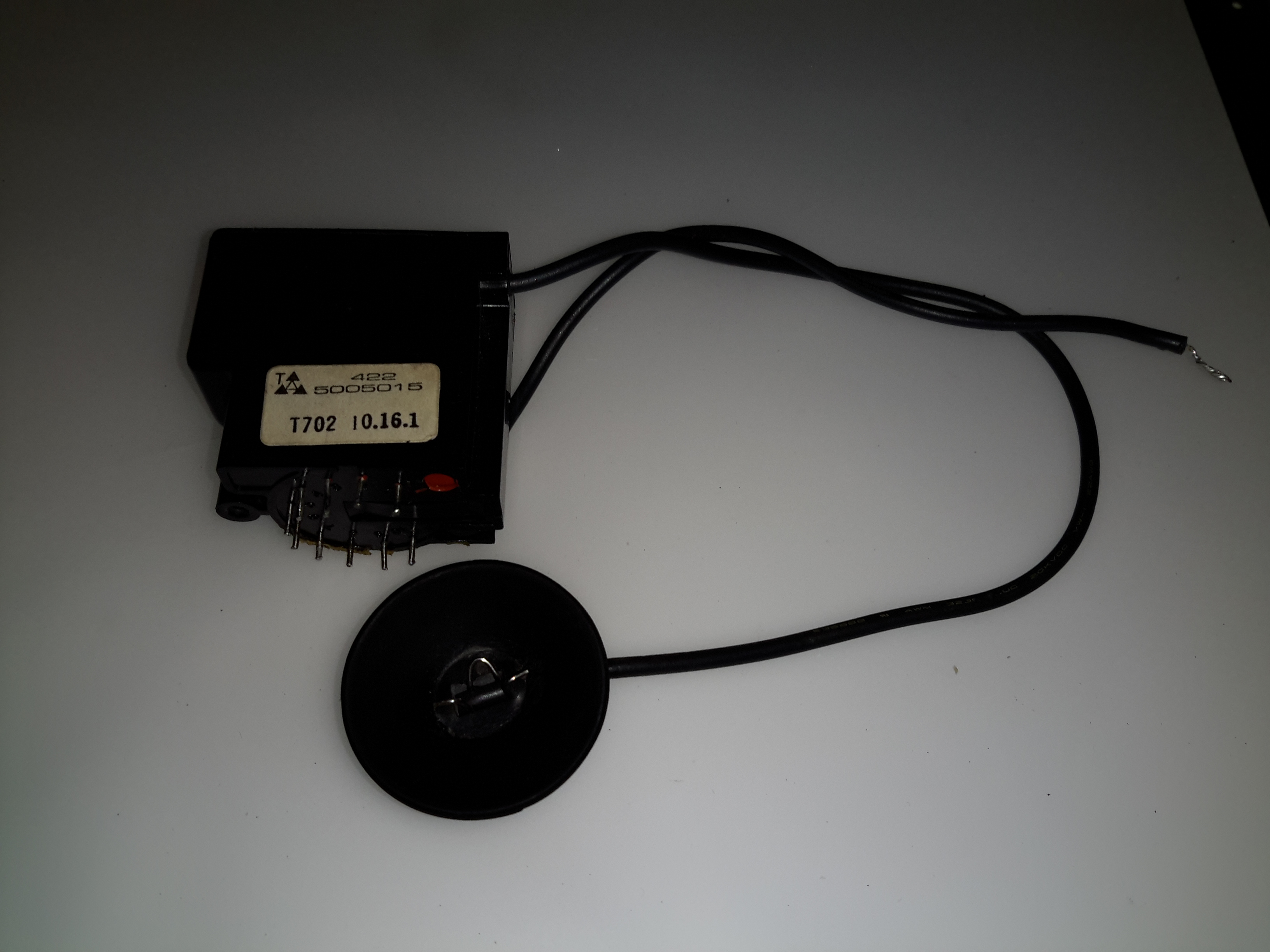
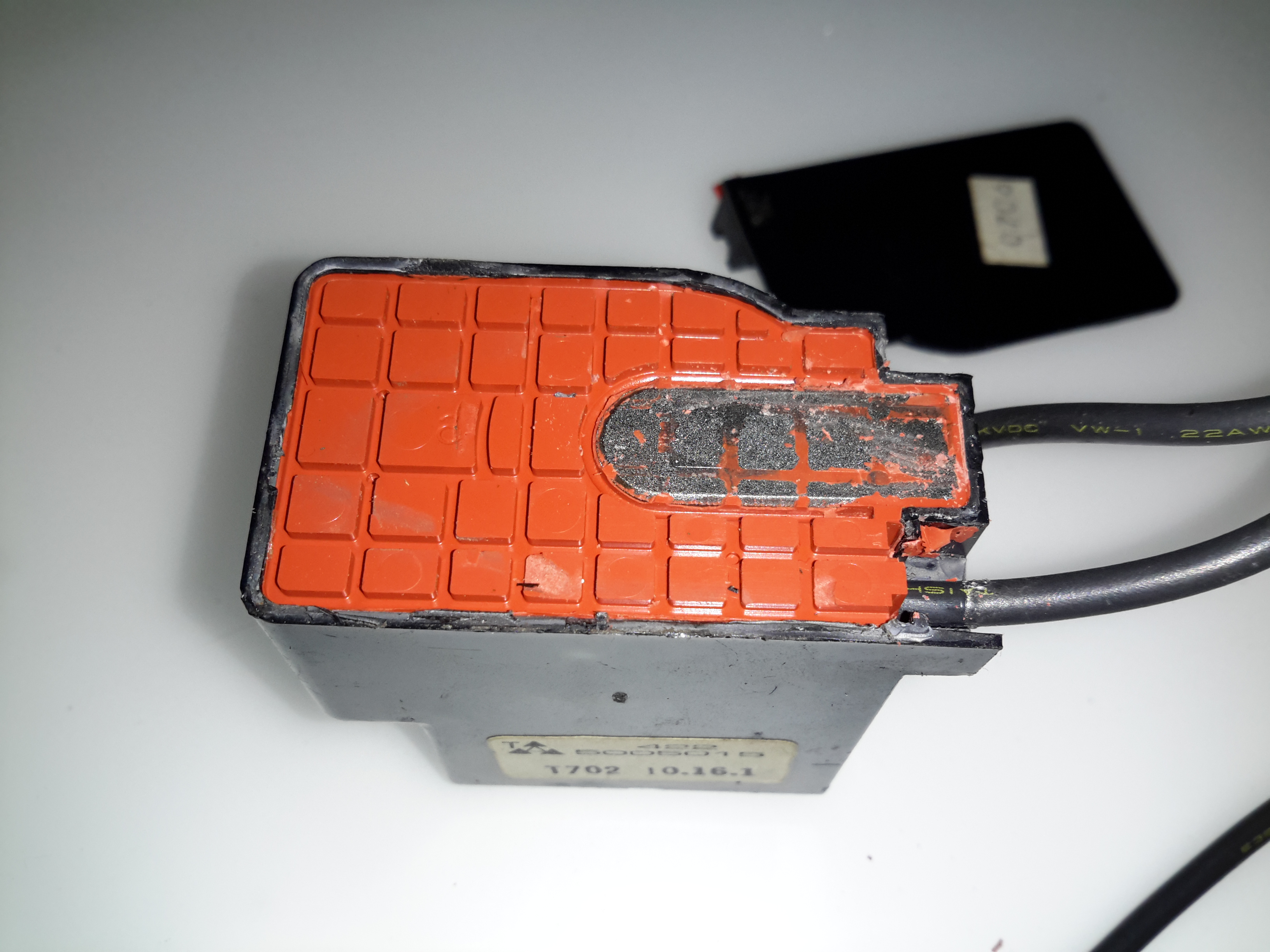
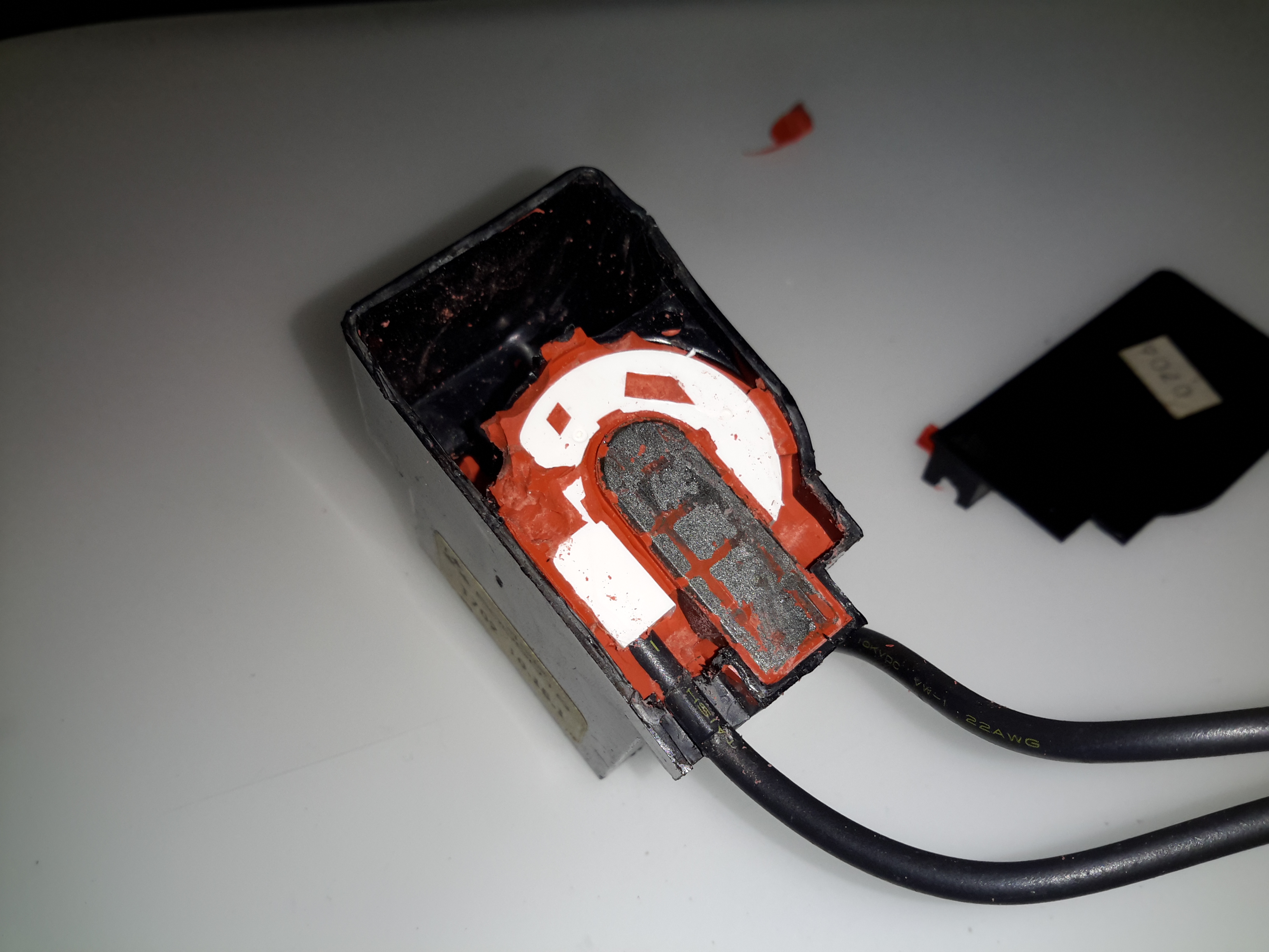
Viewfinder
Viewfinder Assembly
As usual with these cameras, this section is the CRT based viewfinder. These units take the composite signal from the camera to display the scene. This one has many more pins than the usual viewfinder. I’ll hack a manual input into this, but I’ll leave that for another post.
Viewfinder Circuits
Being an older camera than the ones I’ve had before, this one is on a pair of PCBs, which are both single-sided.
Main Viewfinder Board
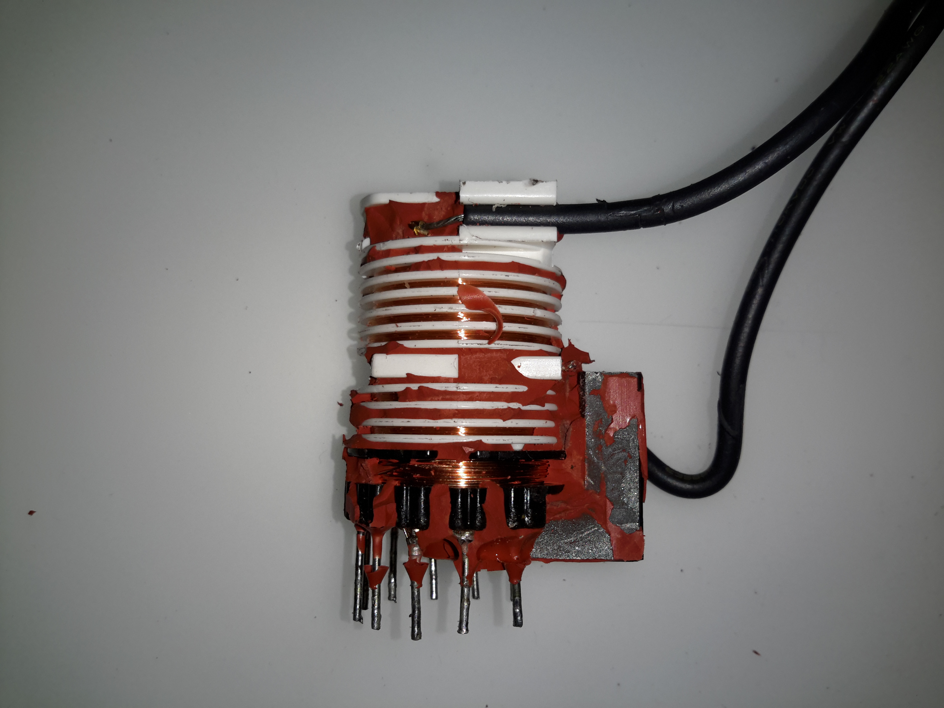
The main board has all the power components for driving the CRT & some of the adjustments. The main HV flyback transformer is on the right. This part creates both the final anode voltage for the tube & the focus/grid voltages.
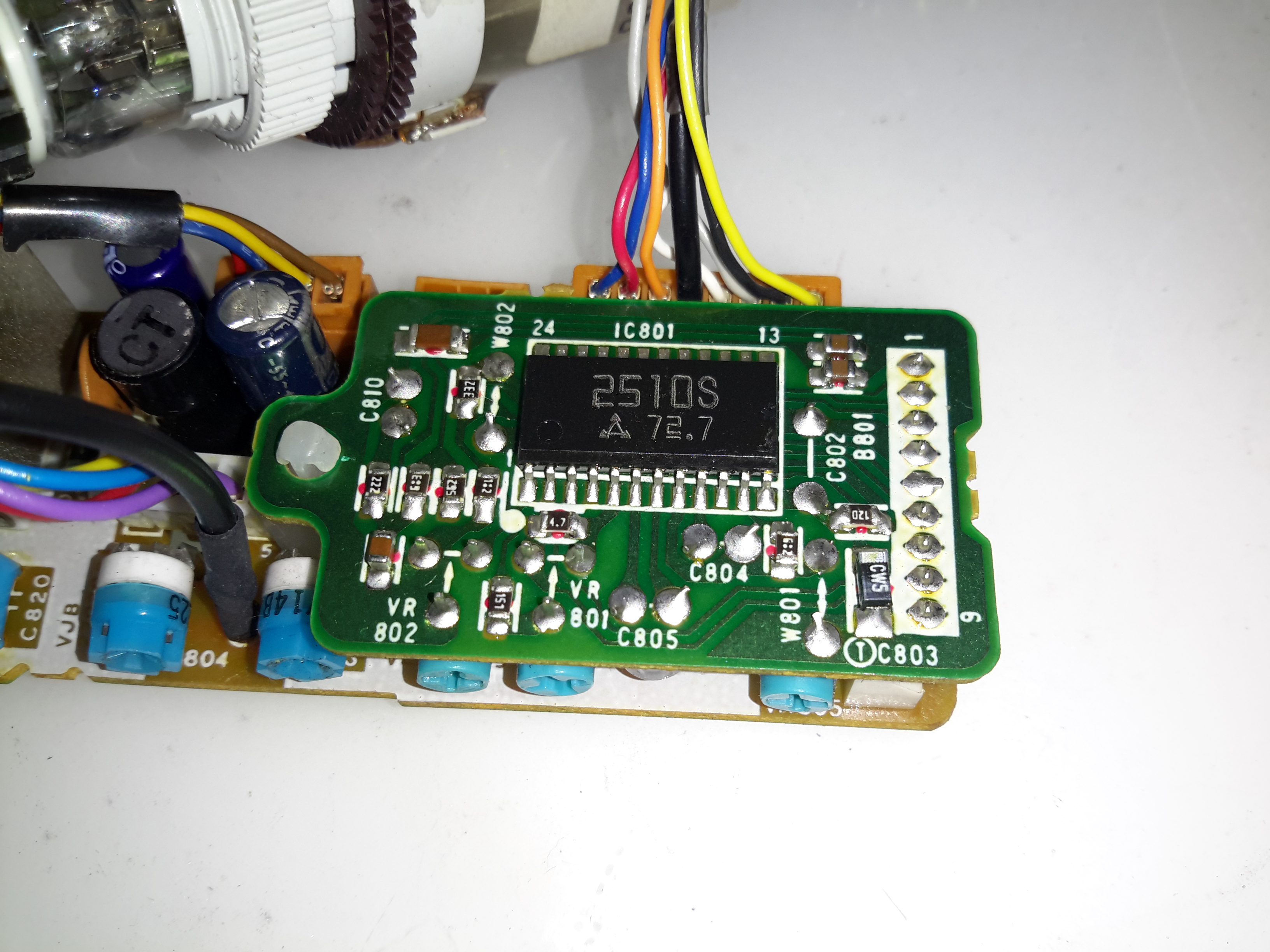
Viewfinder Control PCB Top
The viewfinder control IC is on a separate daughter board in this camera, with two more controls.
Control IC
The control IC is a Matsushita AN2510S, this has all the logic required to separate the sync pulses from the composite signal & generate an image on the CRT.
Viewfinder CRT Frame
The recording indicator LEDs are mounted in the frame of the CRT & appear above the image in the viewfinder.
Viewfinder CRT With Yoke
Here the CRT has been separated from the rest of the circuitry with just the deflection yoke still attached.
M01JPG5WB CRT
The electron gun in this viewfinder CRT is massive in comparison to the others that I have seen, and the neck of the tube is also much wider. These old tubes were very well manufactured.
Viewfinder Optics
A simple mirror & magnifying lens completes the viewfinder unit.
Here’s a small flyback / Line Output Transformer from a portable colour TV set. Usually these transformers are vacuum potted in hard epoxy resin & are impossible to disassemble without anything short of explosives. (There are chemical means of digesting cured epoxies, but none of them are pleasant). This one however, was potted in silicone, so with some digging, the structure of the transformer can be revealed.
Cap Removed
The cap was glued on to the casing, but this popped off easily. The top of the core is visible in the silicone potting material.
The Digging Starts
A small screwdriver was used to remove the potting material, while trying not to damage the winding bobbin & core too badly. The bulge in the casing that I originally thought might house a voltage multiplier turns out to be totally empty. The white plastic bobbin is becoming visible around the core.
Bobbin
After some more digging & a lot of mess later, the entire transformer is revealed. The primary & auxiliary secondaries are visible at the bottom of the transformer, next to the pins. These transformers have multiple windings, as they’re used not only for supplying the final anode voltage of several Kilovolts to the CRT, but many of the other associated voltages, for the heater, grids, focus electrodes, etc. These lower voltage windings are on the same part of the core as the primary.
Above those is the main high voltage secondary winding, which looks to be wound with #38-#40AWG wire (about the thinnest available, at 0.07mm diameter. This is wound in many sections of of a few hundred turns each to increase the insulation resistance to the high voltage. The main anode wire emerges from the top of the bobbin.
Output Rectifier
Hidden in a recess at the top is the main HV rectifier, which on this small transformer is a single device (it’s probably not internally, most likely a series stack of diodes to get the PIV rating required).
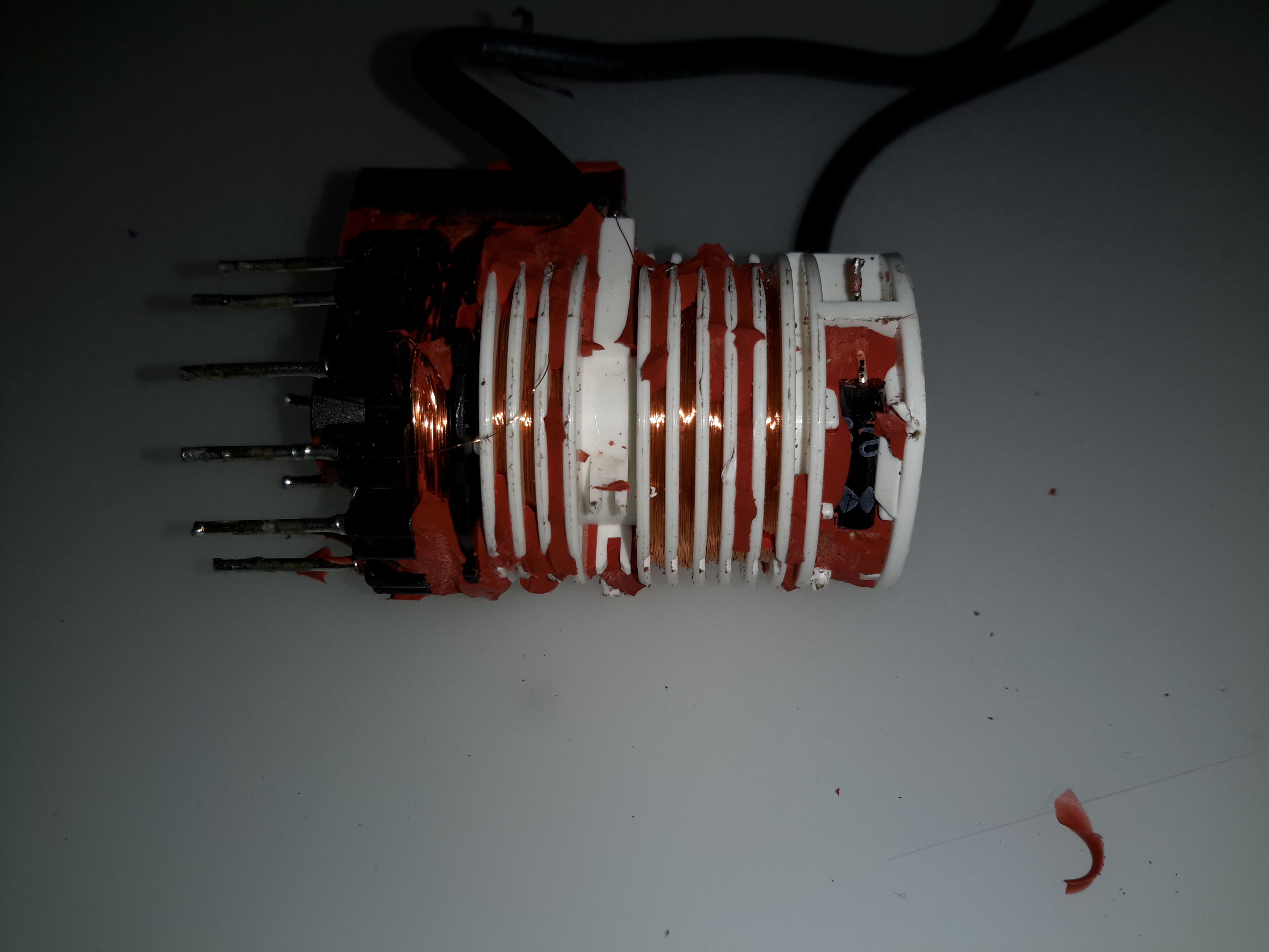
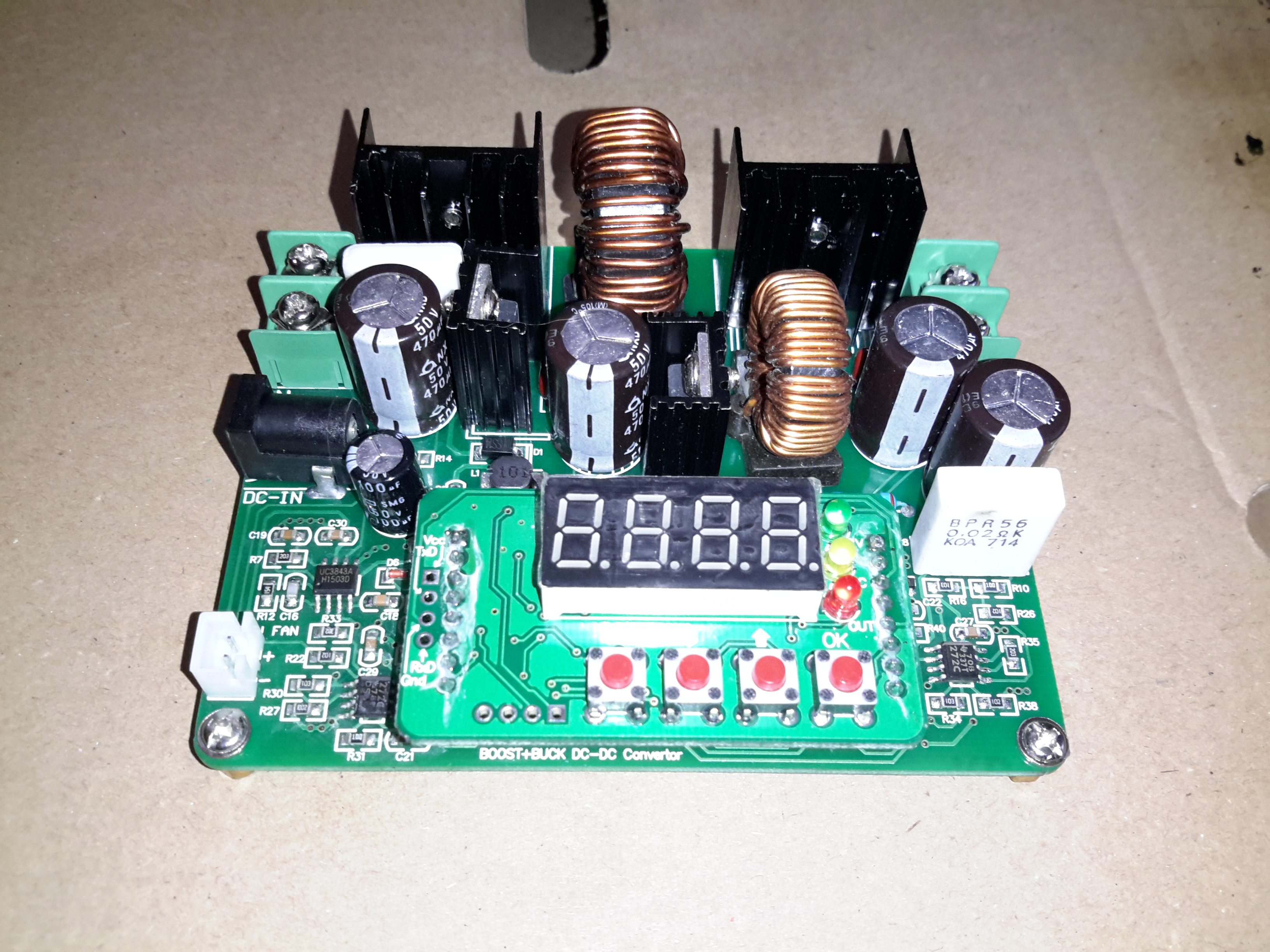
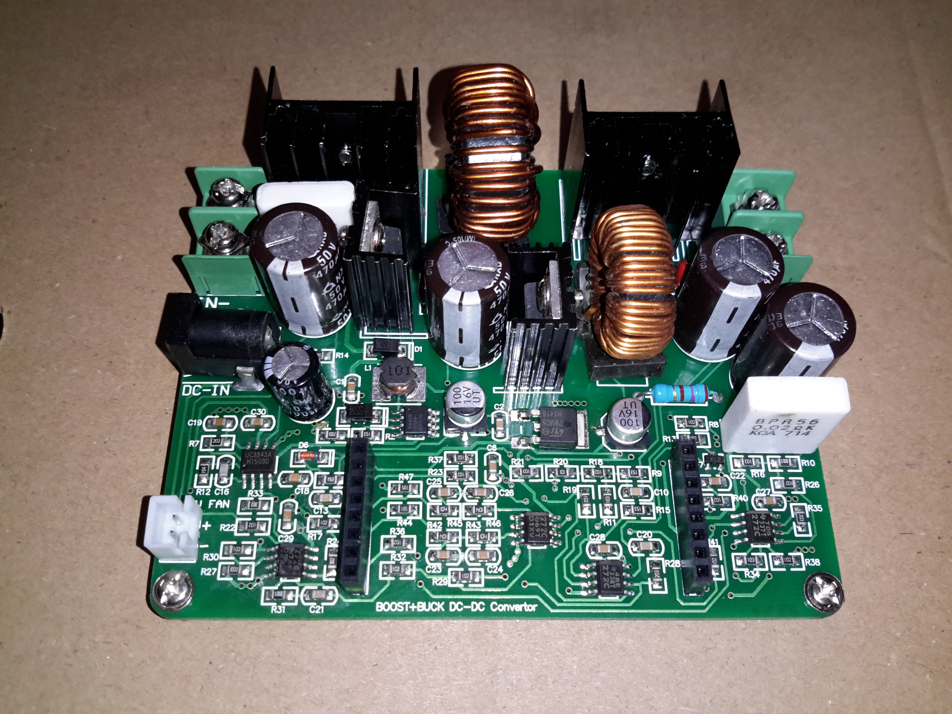
Here’s a useful buck-boost DC-DC converter from eBay, this one will do 36v DC at 6A maximum output current. Voltage & current are selected on the push buttons, when the output is enabled either the output voltage or the output current can be displayed in real time.
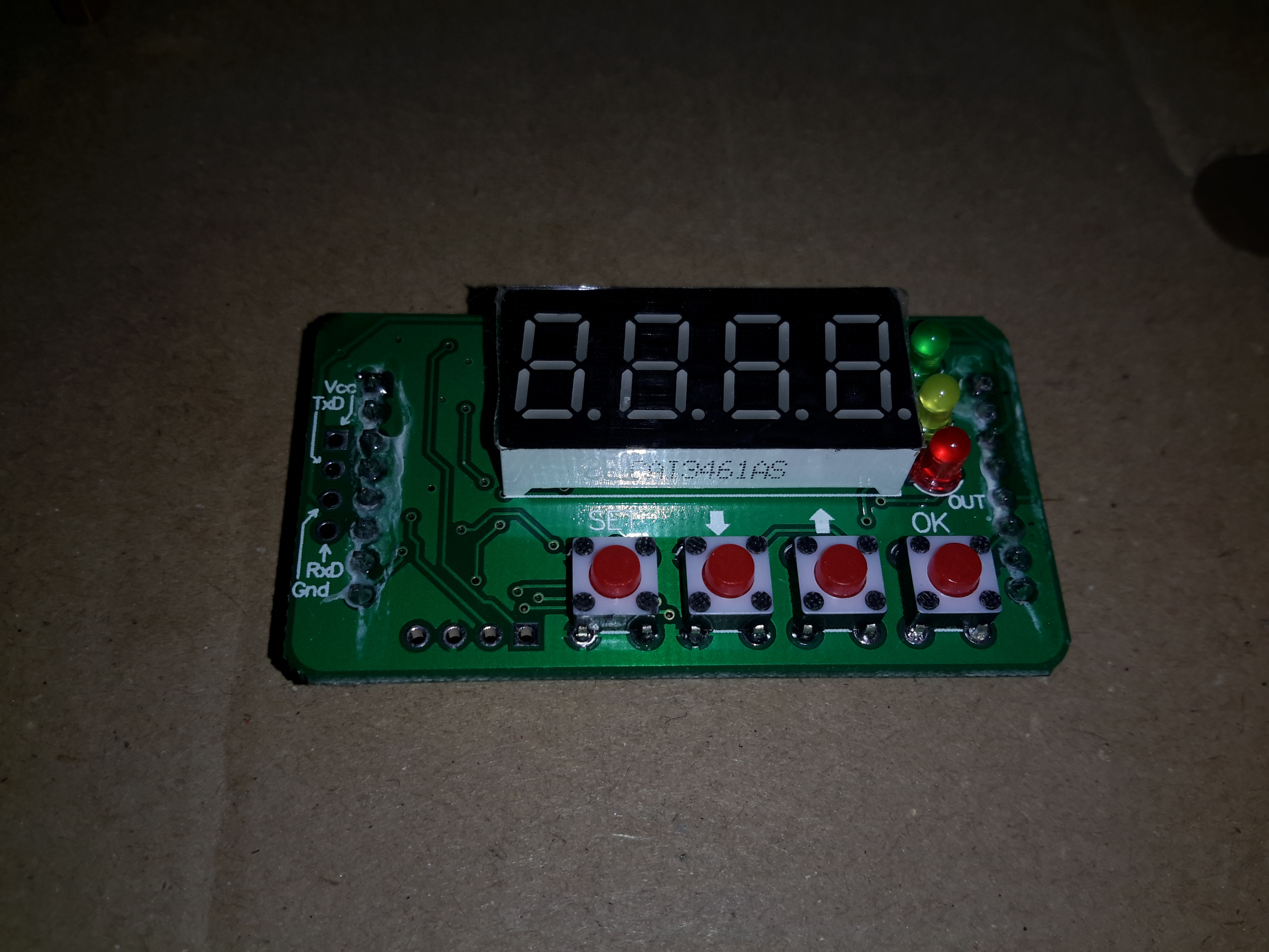
Display PCB
Here’s the display PCB, which also has the STM32 microcontroller that does all the magic. There appears to be a serial link on the left side, I’ve not yet managed to get round to hooking it into a serial adaptor to see if there’s anything useful on it.
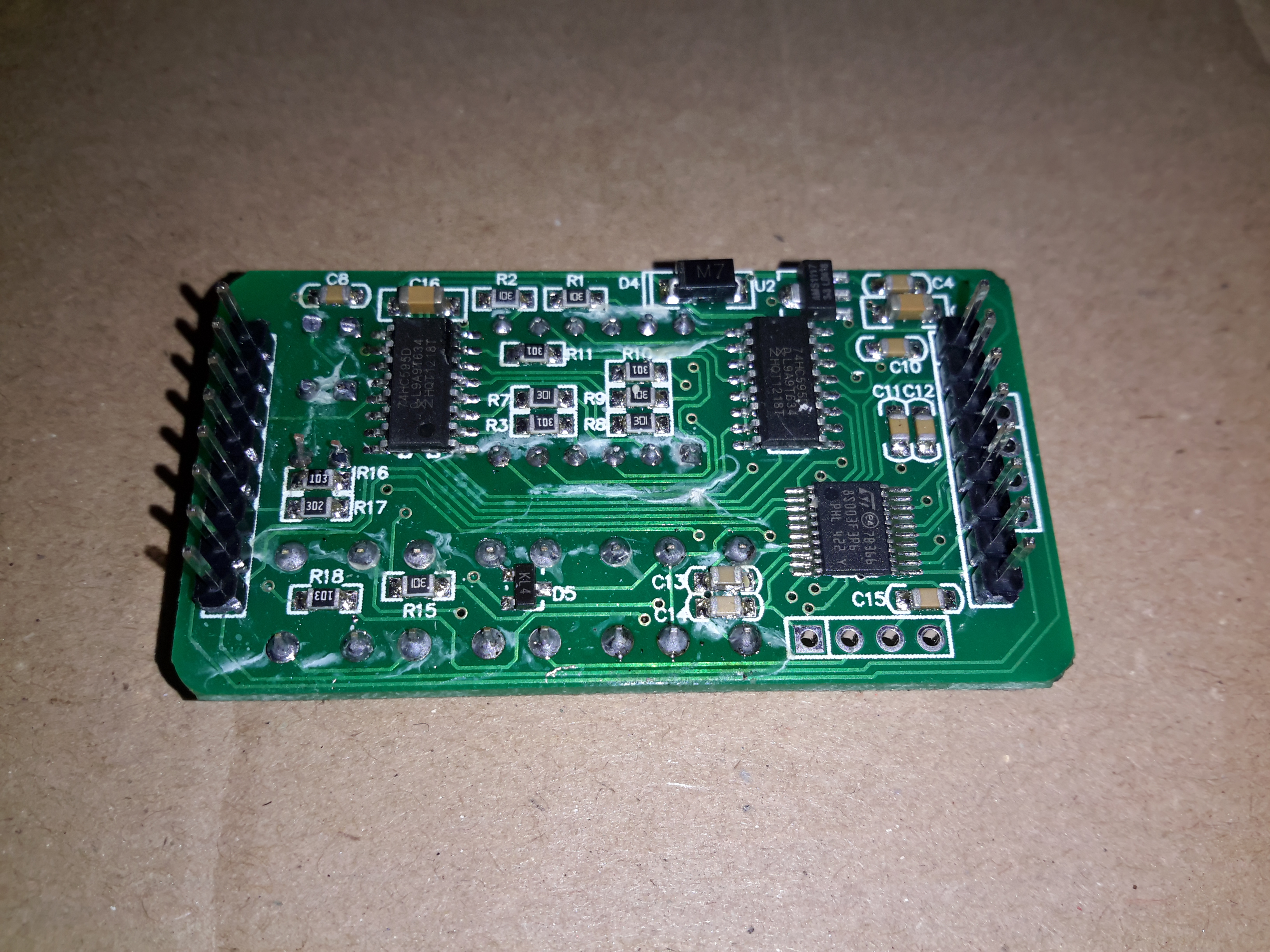
Display Drive & Microcontroller
The bottom of the board holds the micro & the display multiplexing glue logic.
Main PCB
Not much on the mainboard apart from the large switching inductors & power devices. There’s also a SMPS PWM controller, probably being controlled from the micro.
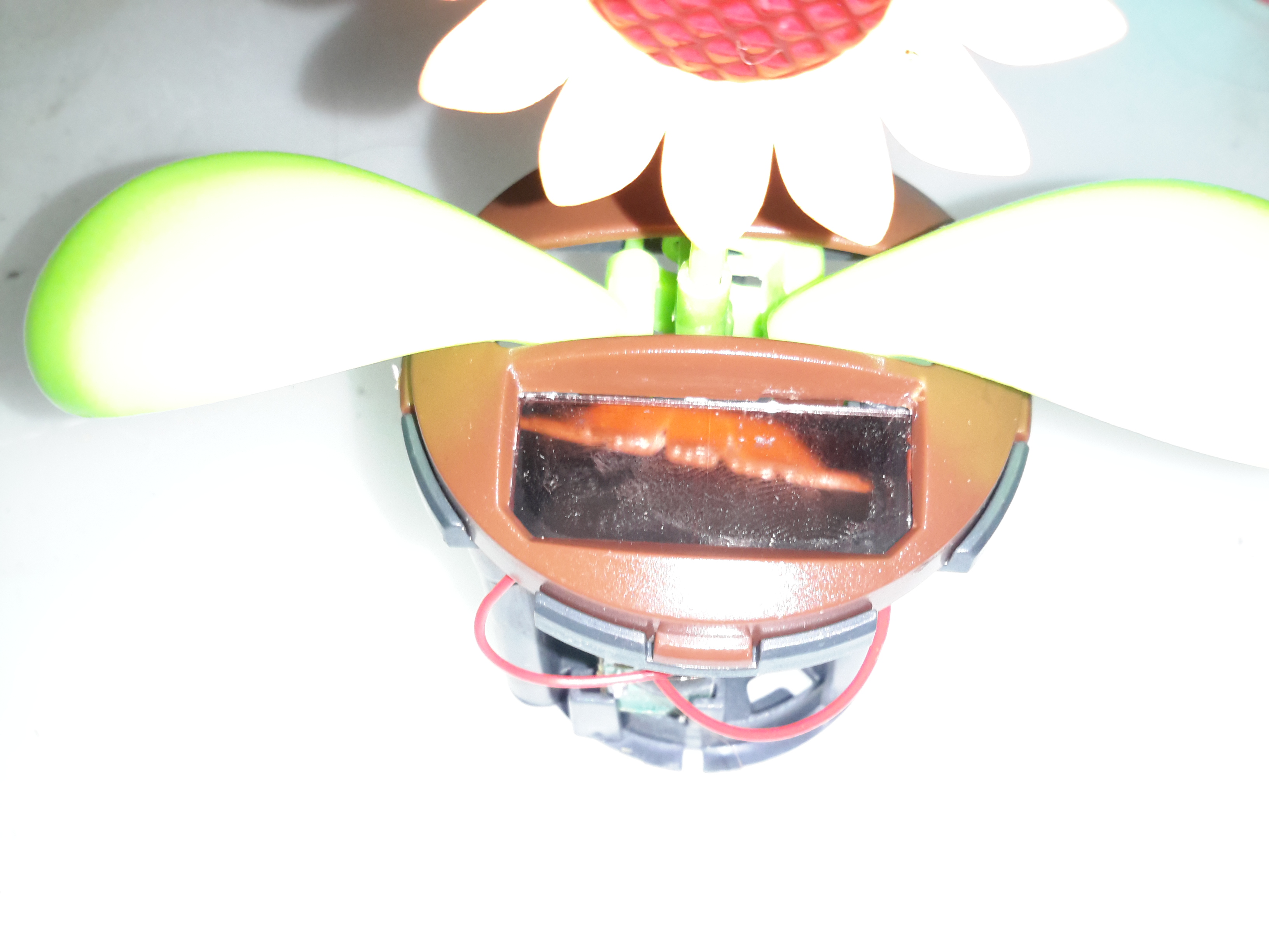
These solar flowers were being sold off at my local Tesco, a pair of them appeared thanks to my child 😉
They have a small solar panel on top, when they’re exposed to bright light, the flower & leaves move as if they’re being blown in a breeze.
Since one of them didn’t work, I figured I’d tear it down.
Solar Cell
The solar cell on the top is similar if not identical to that used on a cheap calculator.
Controller
Not much to the control PCB. Just an electrolytic for smoothing the DC coming from the solar cell & a COB IC.
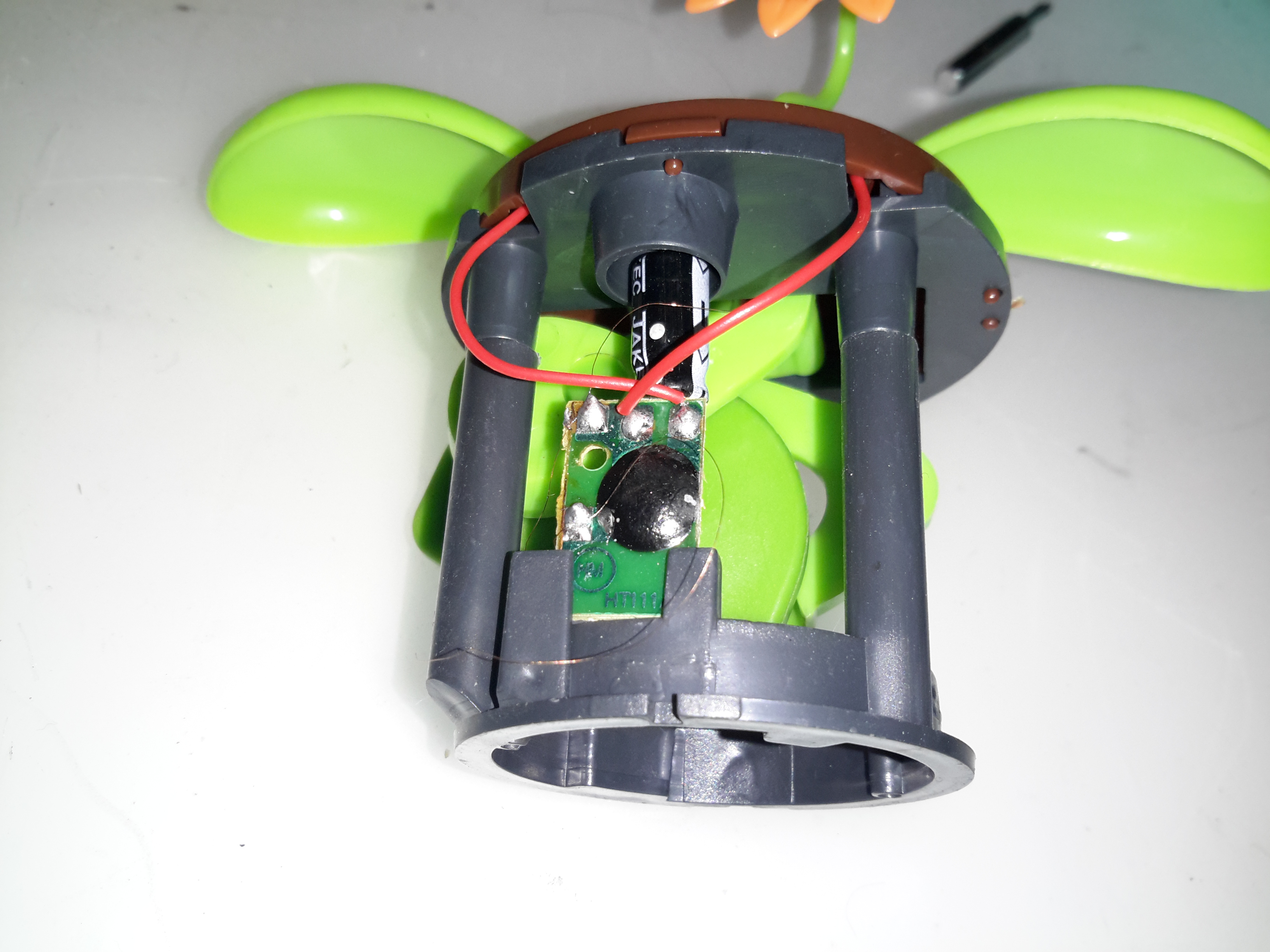
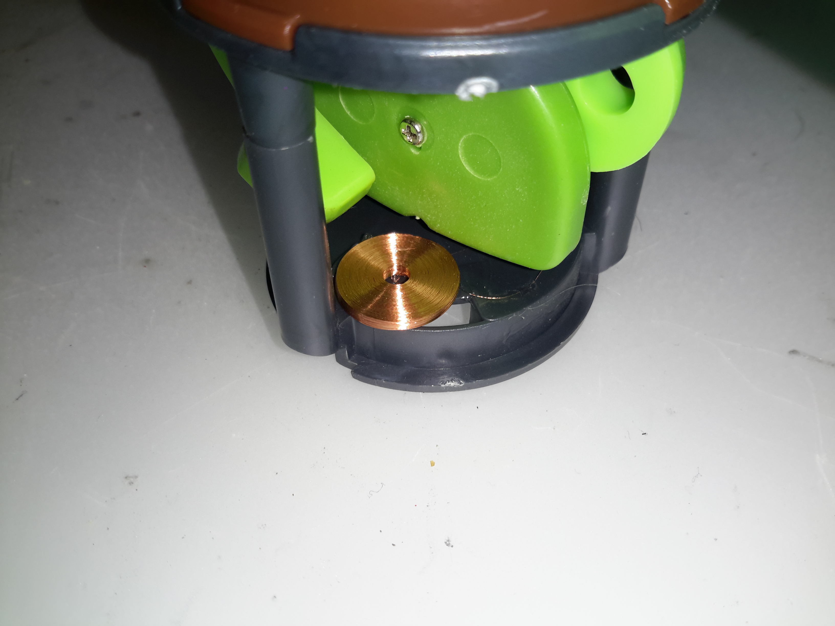
Electromagnet Coil
The IC drives this coil of extremely fine wire, glued to the base of the housing. Attached to the green plastic arm should be a magnet – this one has never worked as the magnet is missing. at 50p a piece, a magnet would cost me more than the whole device. So it’s the bin for this one.
I have found myself needing some more in the way of High Voltage supplies of late, with the acquisition of the new He-Ne laser tubes, so I went trawling eBay for something that would be suitable to run these tubes. (I currently only have a single He-Ne laser PSU brick, and they’re notoriously hard to find & rather expensive).
This supply is rated at 1kV-10kV output, at 35W power level. Unfortunately this supply isn’t capable of sustaining the discharge in a large He-Ne tube, the impedance of the supply is far too high. Still, it’s useful for other experiments.
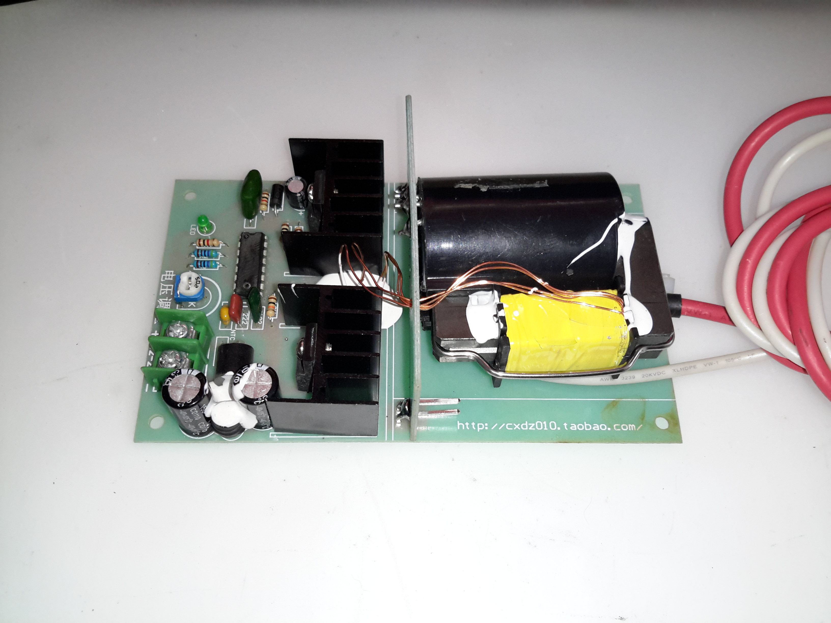
The flyback-type transformer clearly isn’t a surplus device from CRT manufacture, as there are very few pins on the bottom, and none of them connect to the primary side. The primary is separately wound on the open leg of the ferrite core.
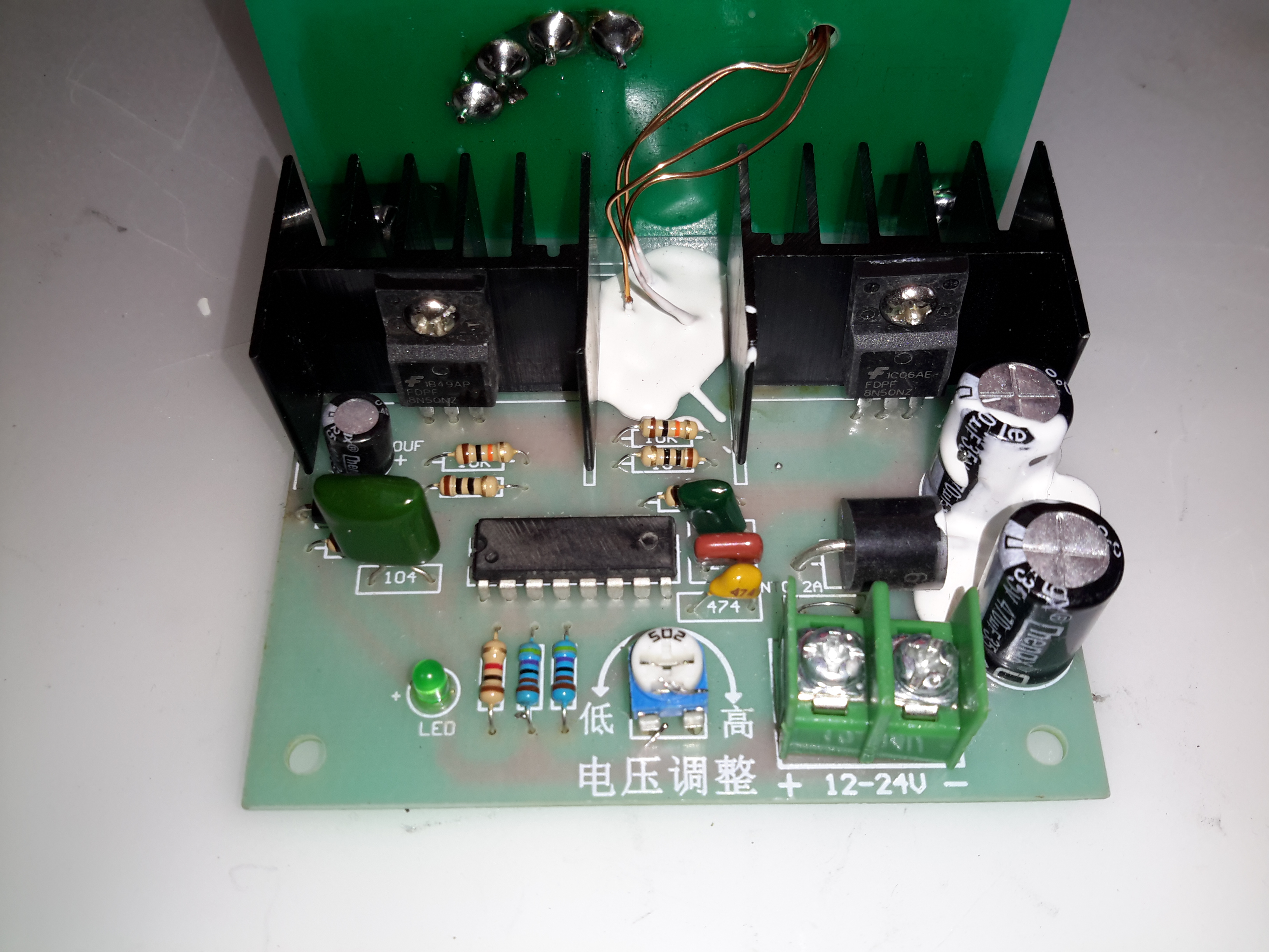
Drive Electronics
The drive electronics are pretty simple, there’s a controller IC (with the number scrubbed off – guessing it’s either a 556 dual timer or a SMPS controller), a pair of FDP8N50NZ MOSFETs driving the centre-tapped primary winding.
The drive MOSFETs aren’t anything special in this case: they’re rated at 500v 8A, 850mΩ on resistance. This high resistance does make them get rather hot even with no load on the output, so for high power use forced-air cooling from a fan would definitely be required.
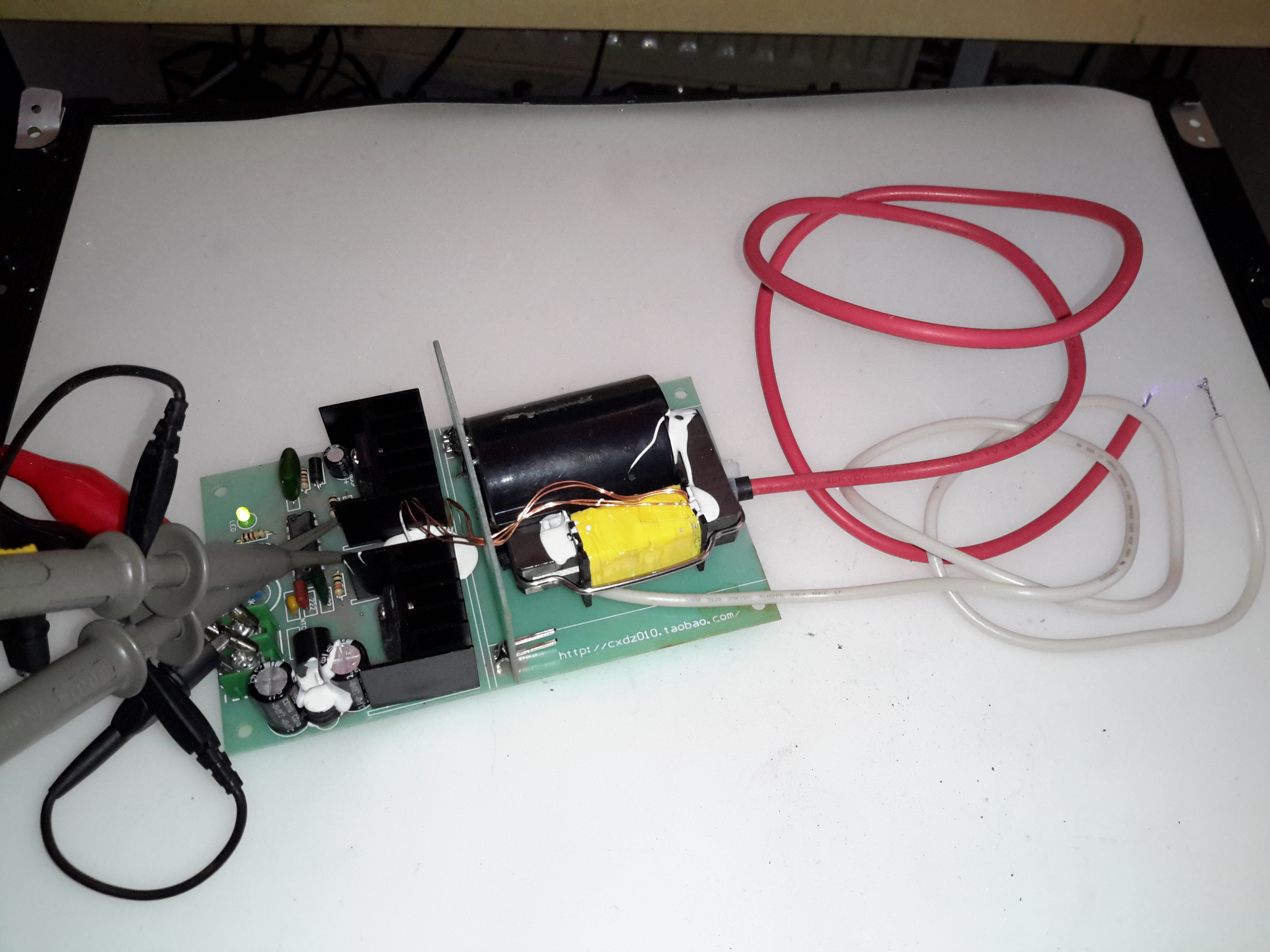
Test Setup
Here’s the supply on test, I’ve got the scope probes connected to the gate resistors of the drive MOSFETs.
Waveforms
On the scope the primary switching waveforms can be seen. The FETs operate in push-pull mode, there’s a bit of a ring on the waveform, but they’re pretty nice square waves otherwise.
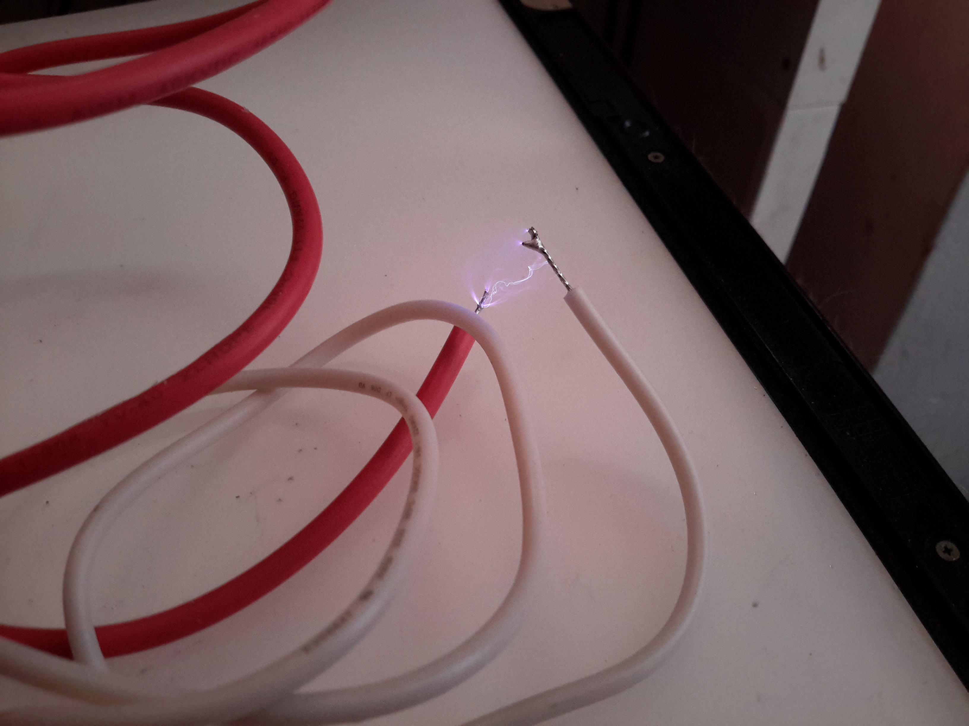
Arc
At maximum power on 12v input, about 25mm of gap is possible with an arc.
Tip Jar
If you’ve found my content useful, please consider leaving a donation by clicking the Tip Jar below!
All collected funds go towards new content & the costs of keeping the server online.