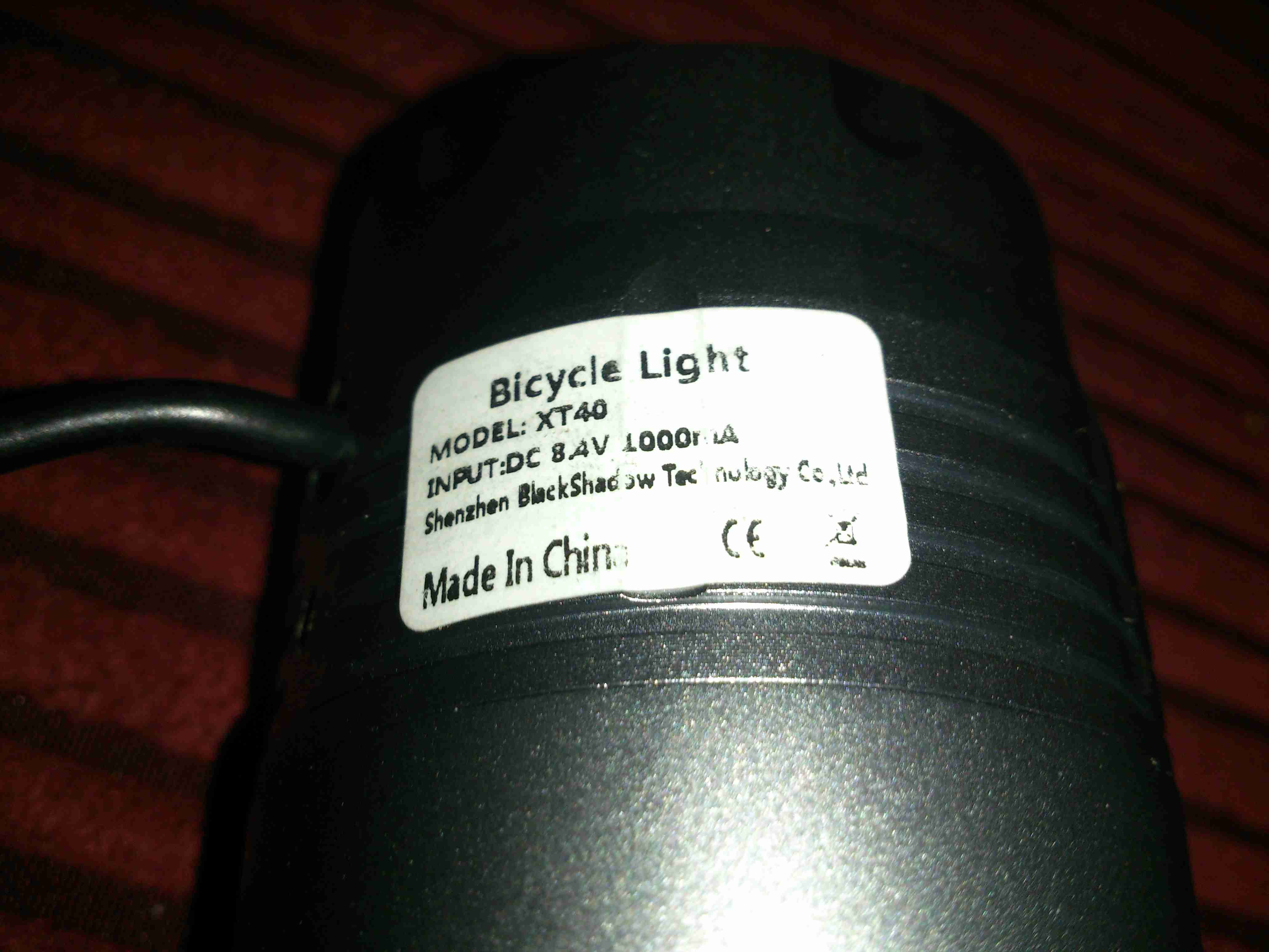
Here’s another torch from eBay, this time with 5 Cree XML-T6 LEDs.
Label
Having 5 Cree LEDs rated at up to 3A a piece, this light has the capacity to draw about 50W from it’s power supply. In this case though, current draw is about 1.5A at 12v input on the full brightness setting.
Cree LED Torch
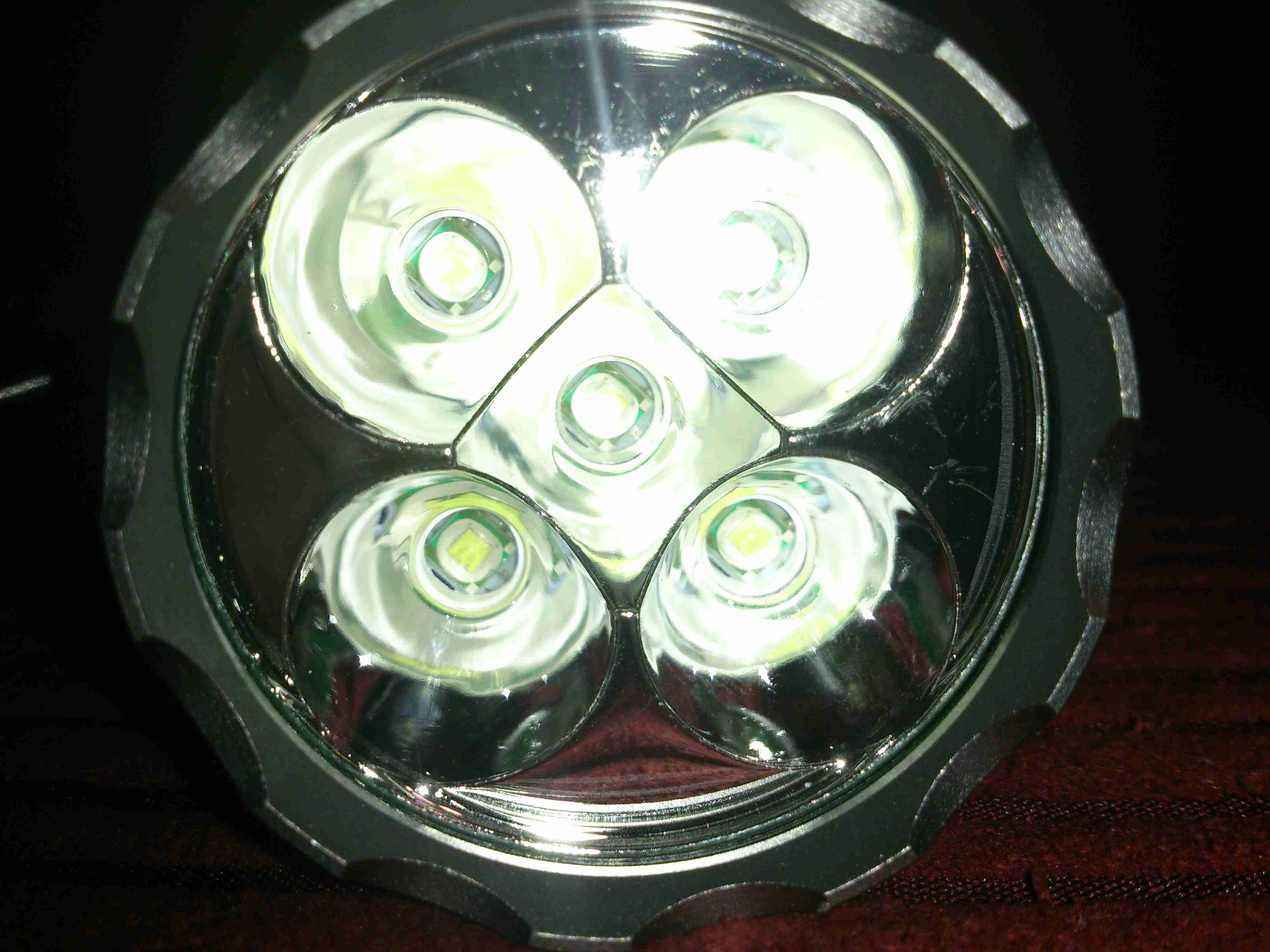
Here’s the LEDs mounted into the reflector. Fitting this many high power LEDs into a small space requires some serious heatsinking. The casing is made of machined aluminium.
LED Module
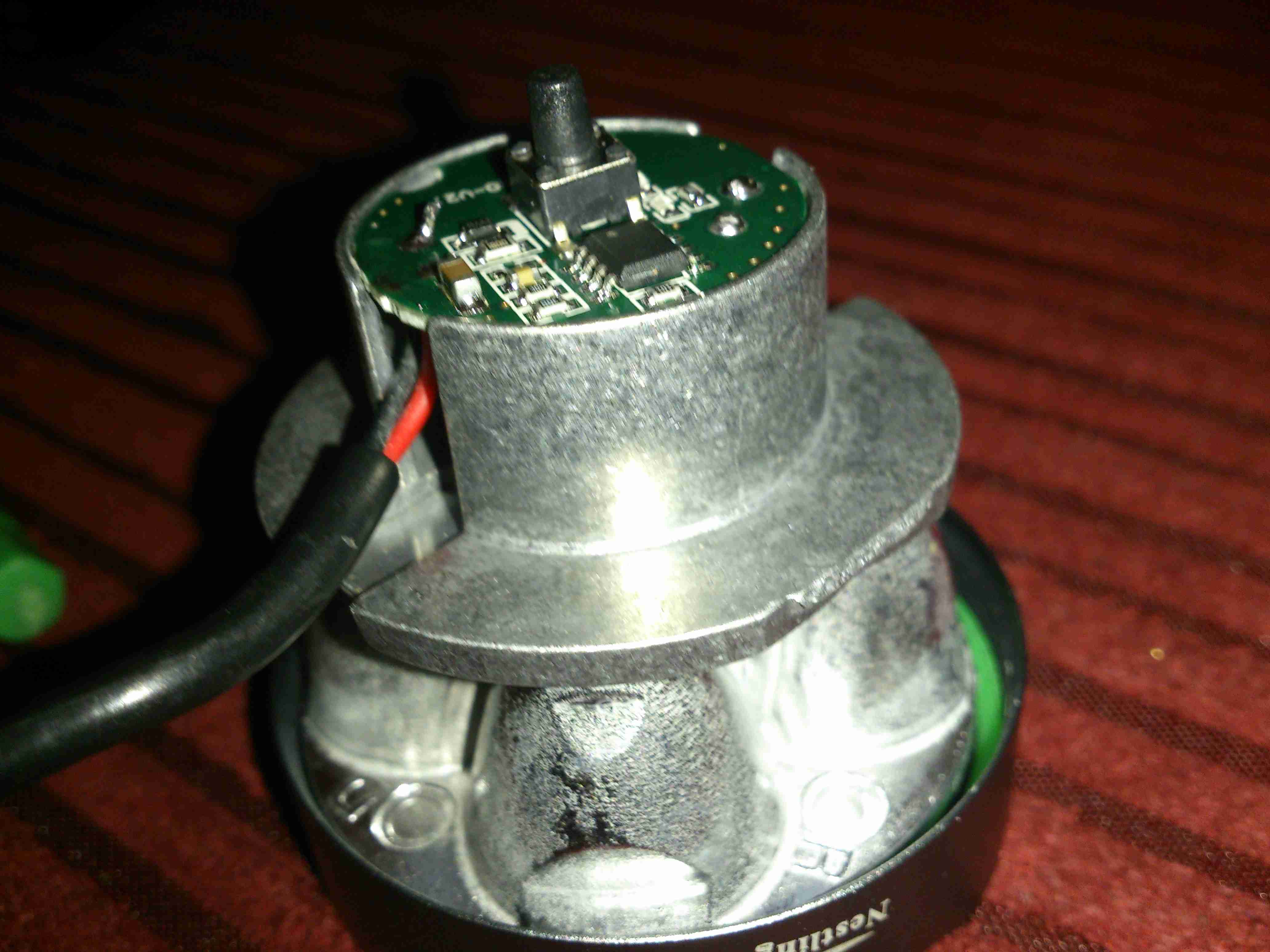
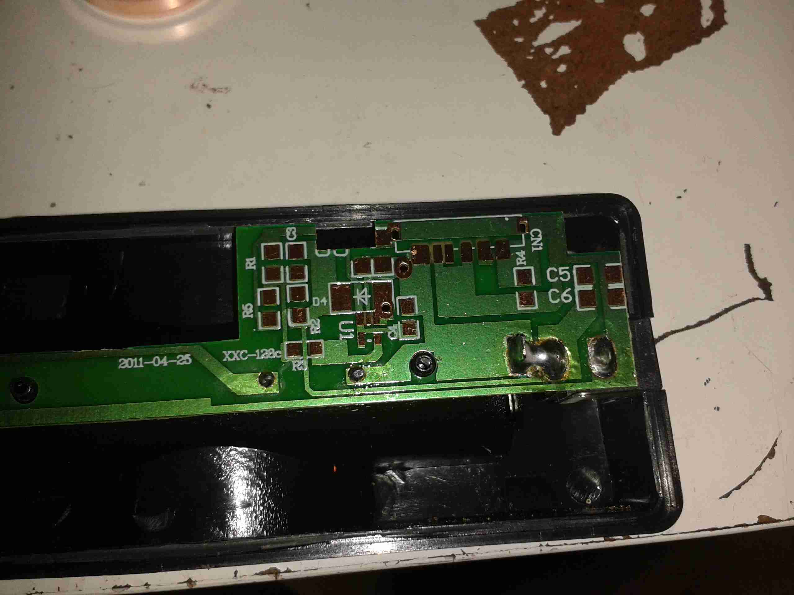
Unscrewing the front bezel allows the internals to come out. The core frame & reflector is all cast alloy as well, for heatsinking the LEDs. The controller PCB is mounted into a recess in the back of the LED mount.
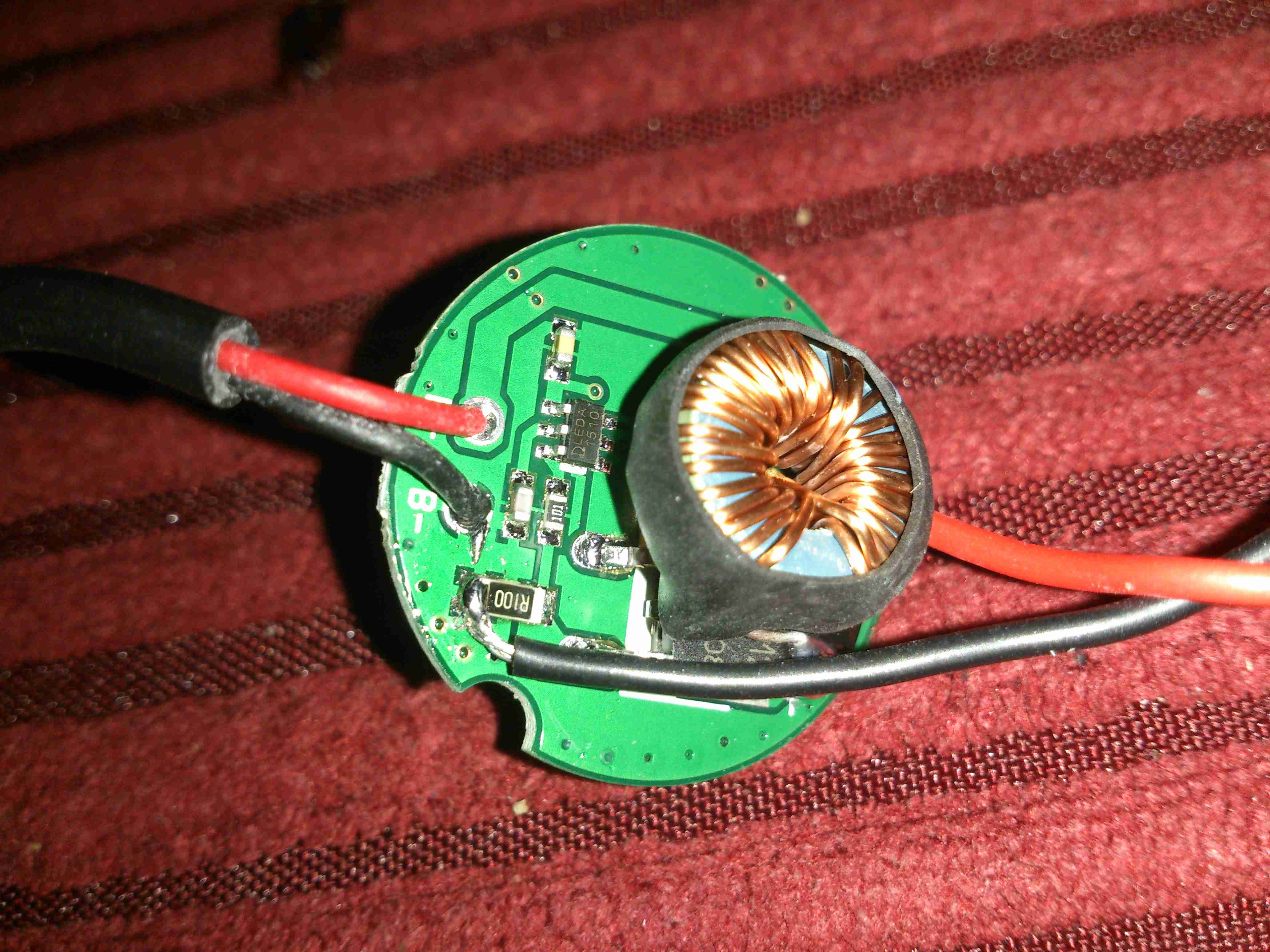
Controller
Here’s the controller itself. The usual small microcontroller is present, for the multiple modes, and handling the momentary power switch.
Switching Inductor
As all the LEDs on this torch are connected in series, their forward voltage is ~12-15v. The battery is an 8.4v Li-Ion pack, so some boost conversion is required. This is handled by the circuitry on the other side of the board, with this large power inductor.
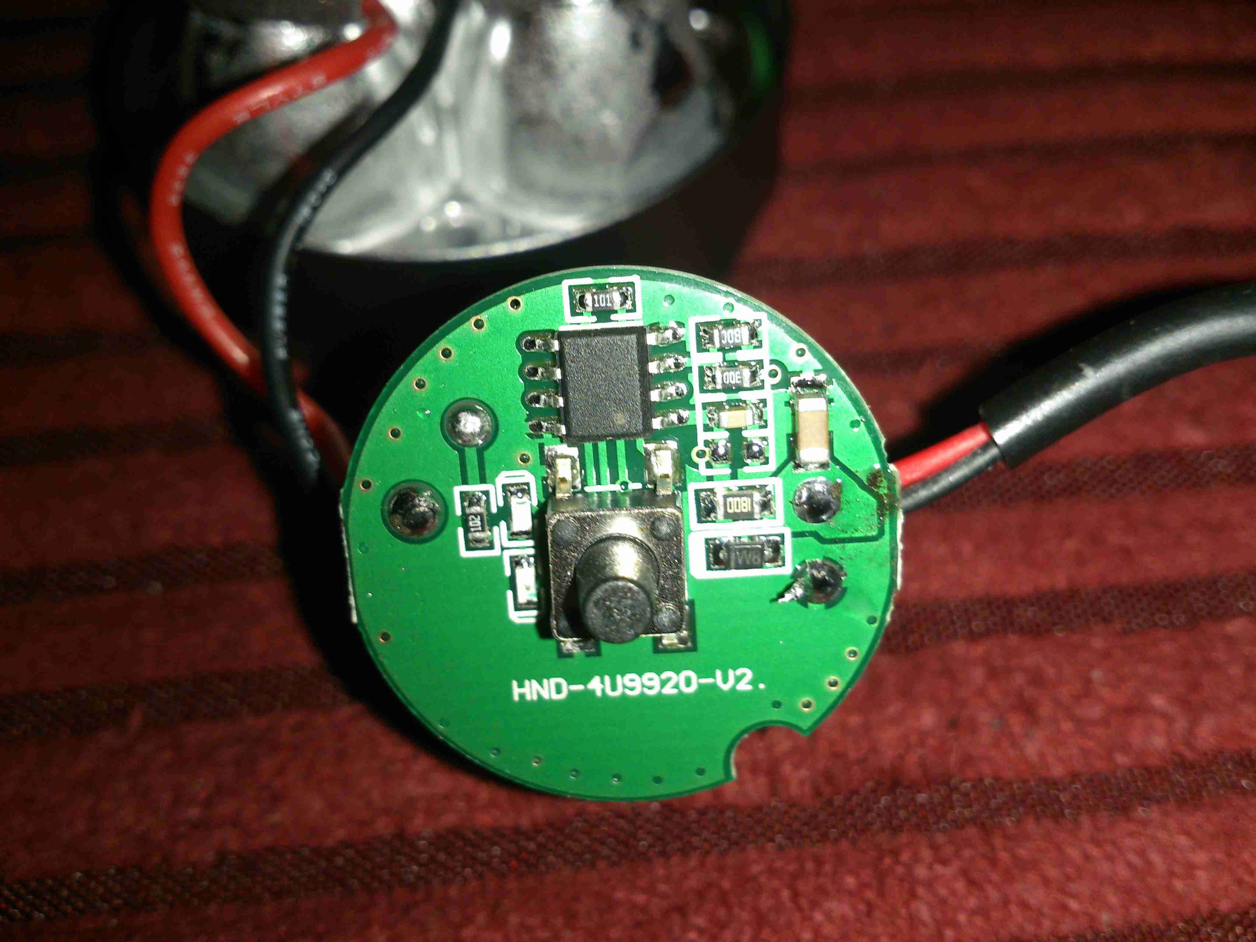
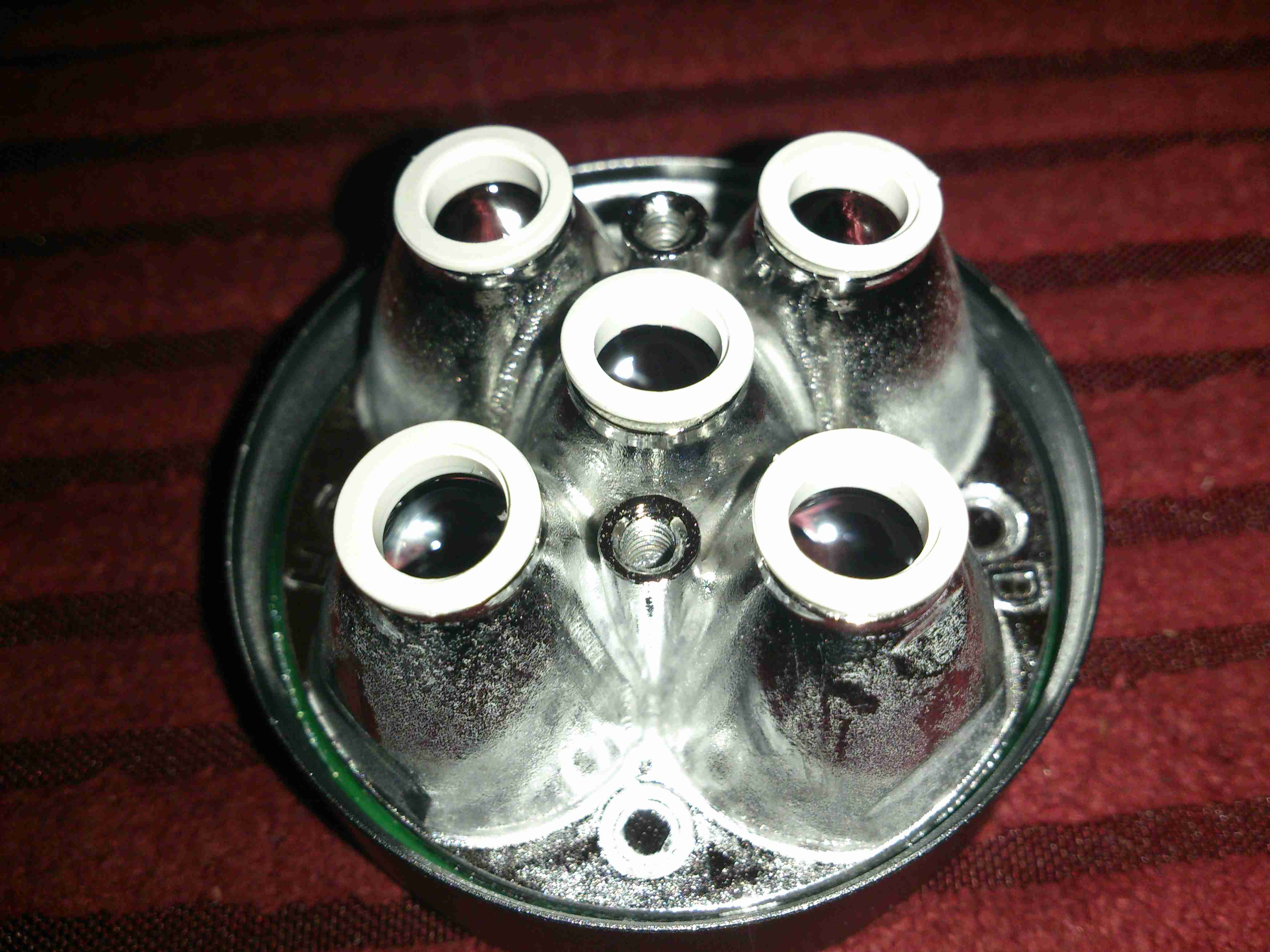
Reflector
The reflector screws onto the front of the LED array, centered in place with some plastic grommets around the LEDs themselves.
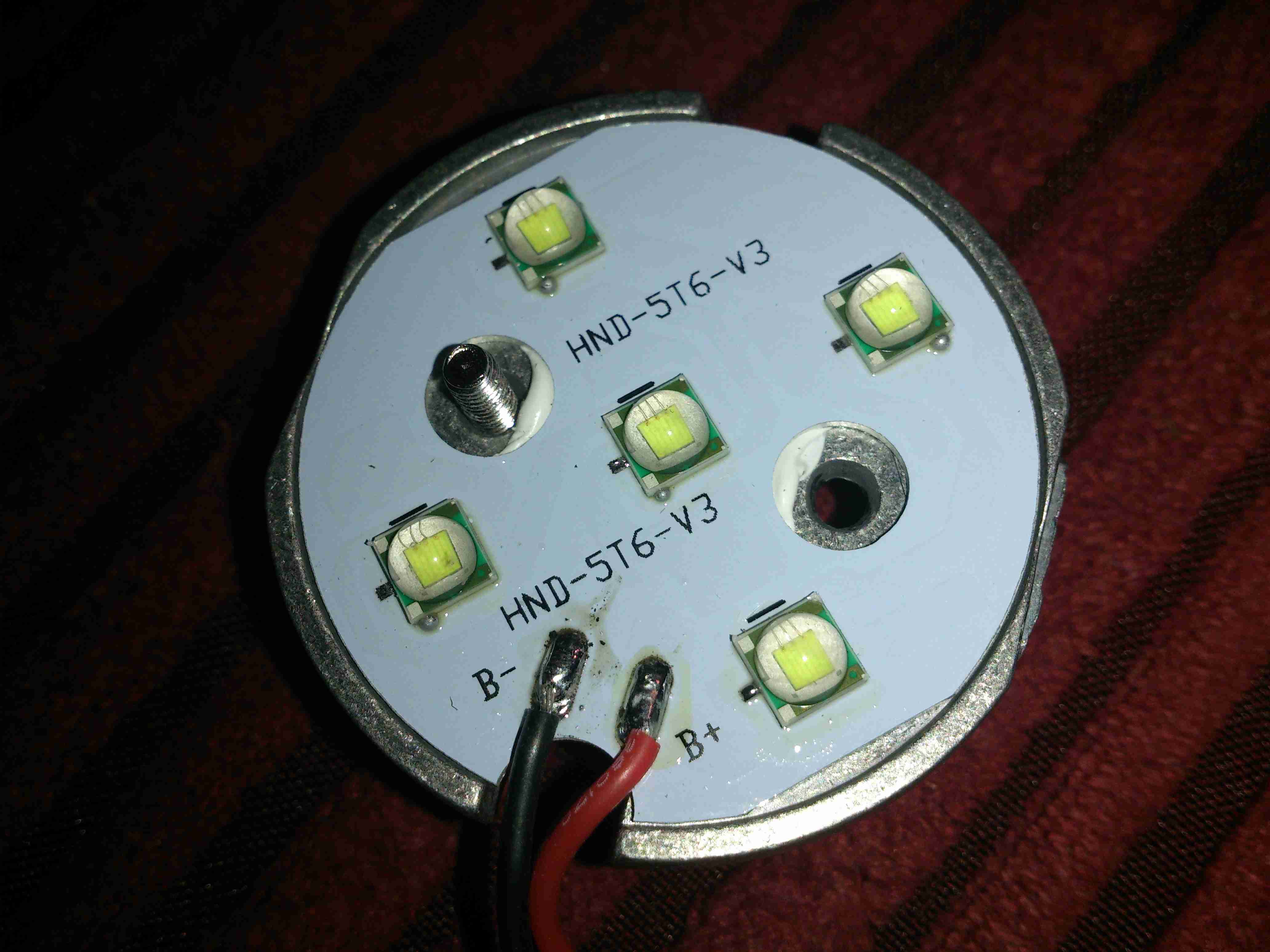
LED Array
Finally for the torch, the LED array itself. This is attached to the frame with some thermal adhesive, and the LEDs themselves are mounted on an aluminium-core PCB for better heat transfer.
This module unsurprisingly generates quite some heat, so I have improved the thermal transfer to the outer case with some thermal grease around the outer edge.
Charger
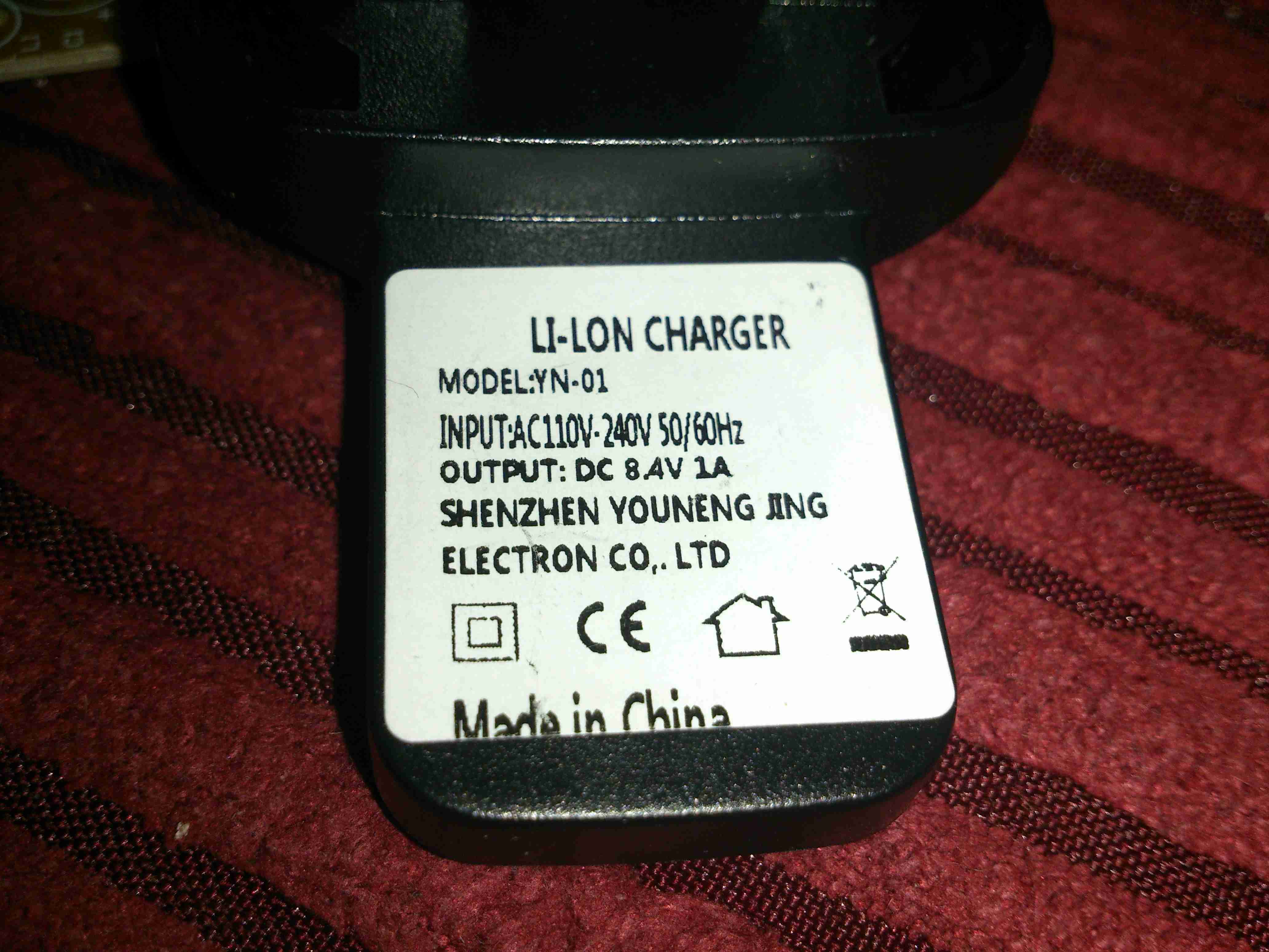
The supplied charger is the usual Chinese cheapy affair, claiming an output current of 1A at 8.4v. I never use these chargers, so they get butchered instead.
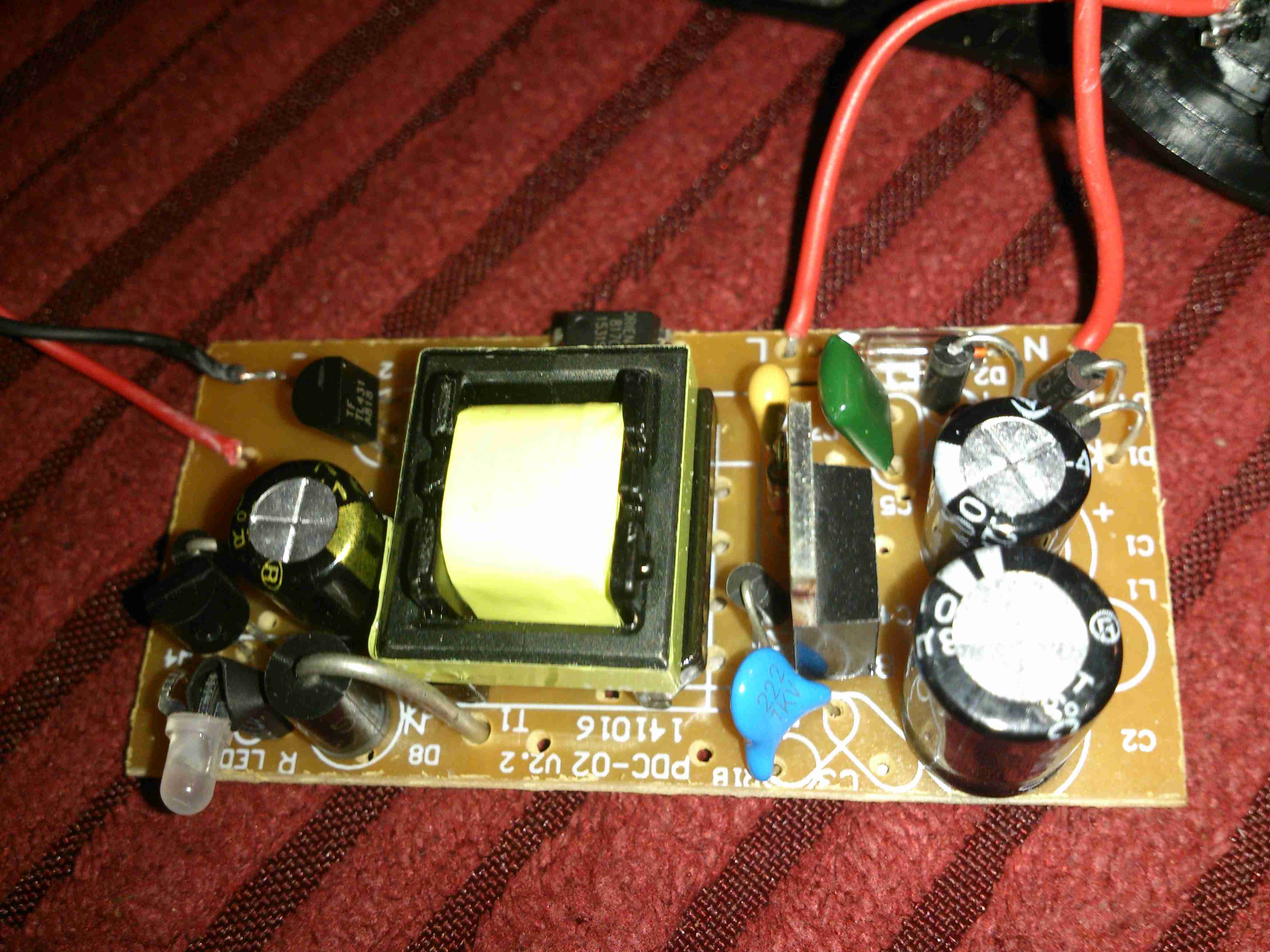
Charger PCB
Here’s the main PCB. Overall the construction isn’t that bad, the input mains is full-wave rectified, but there is little in the way of RFI filtering. The supply is fused, but with an absolutely tiny glass affair that I seriously doubt has the ability to clear a large fault current.
Like many cheap supplies, the output wiring is very thin, it’s capacity to carry 1A is questionable.
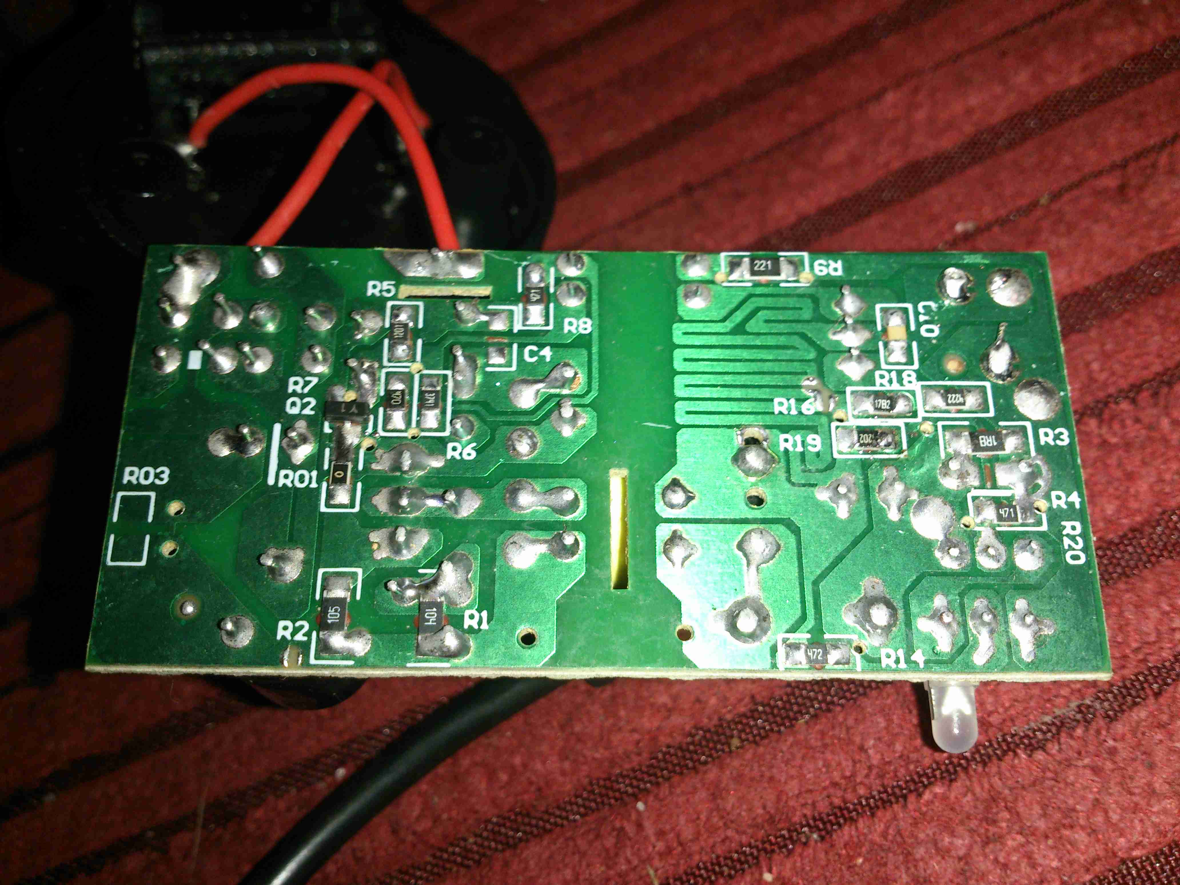
PCB Reverse
On the reverse side, there’s a nice large gap between the mains side & the low voltage output. There’s even an anti-tracking slot under the optoisolator.
I almost forgot about this bit of kit, that came with one of my LED torches as a Lithium Ion charger. As I never plug in anything that comes from China via eBay, here’s the teardown & analysis.
Another Lethal Charger?
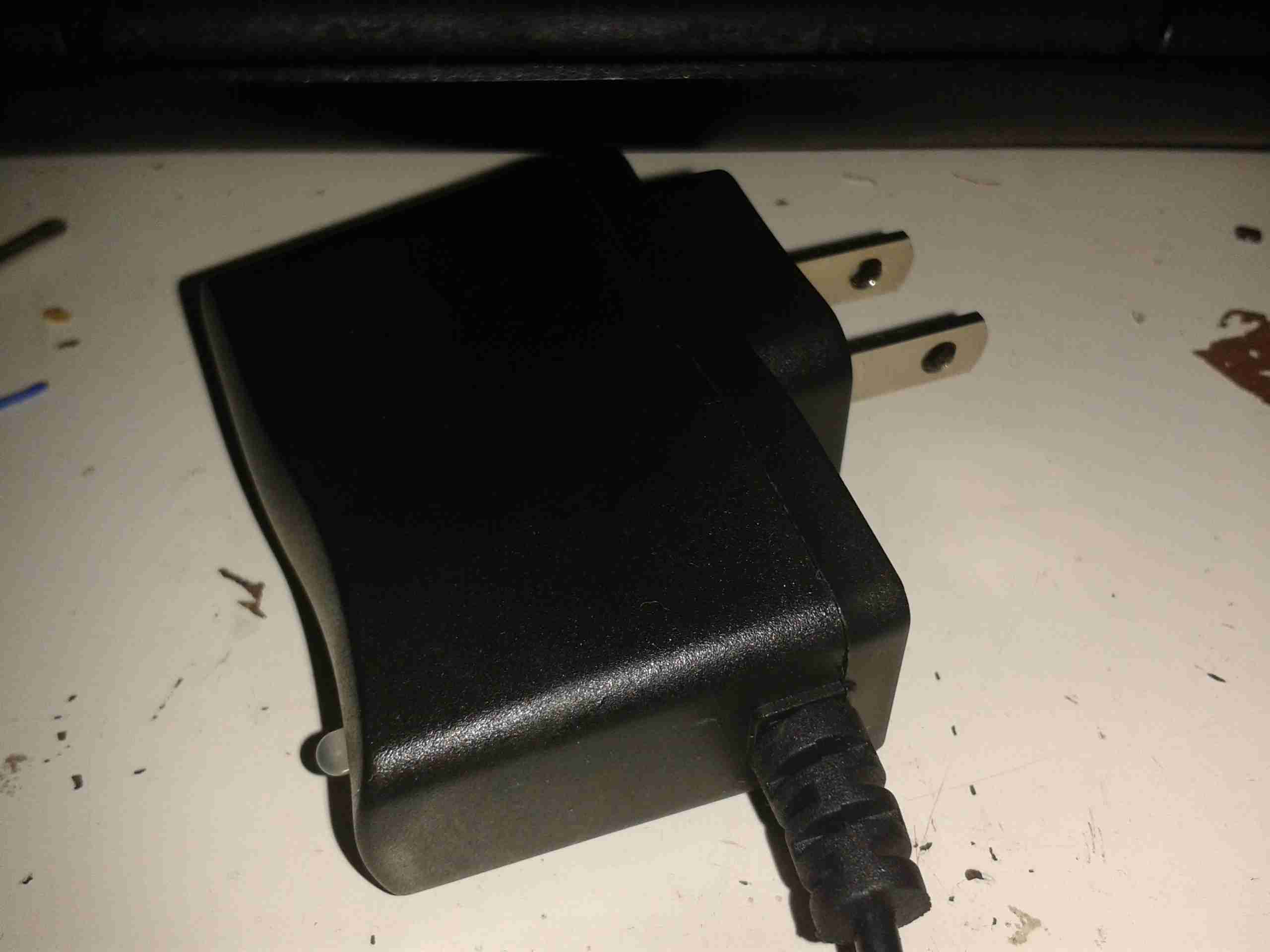
Here’s the unit itself. It’s very light, and is clearly intended for American NEMA power points.
Specs
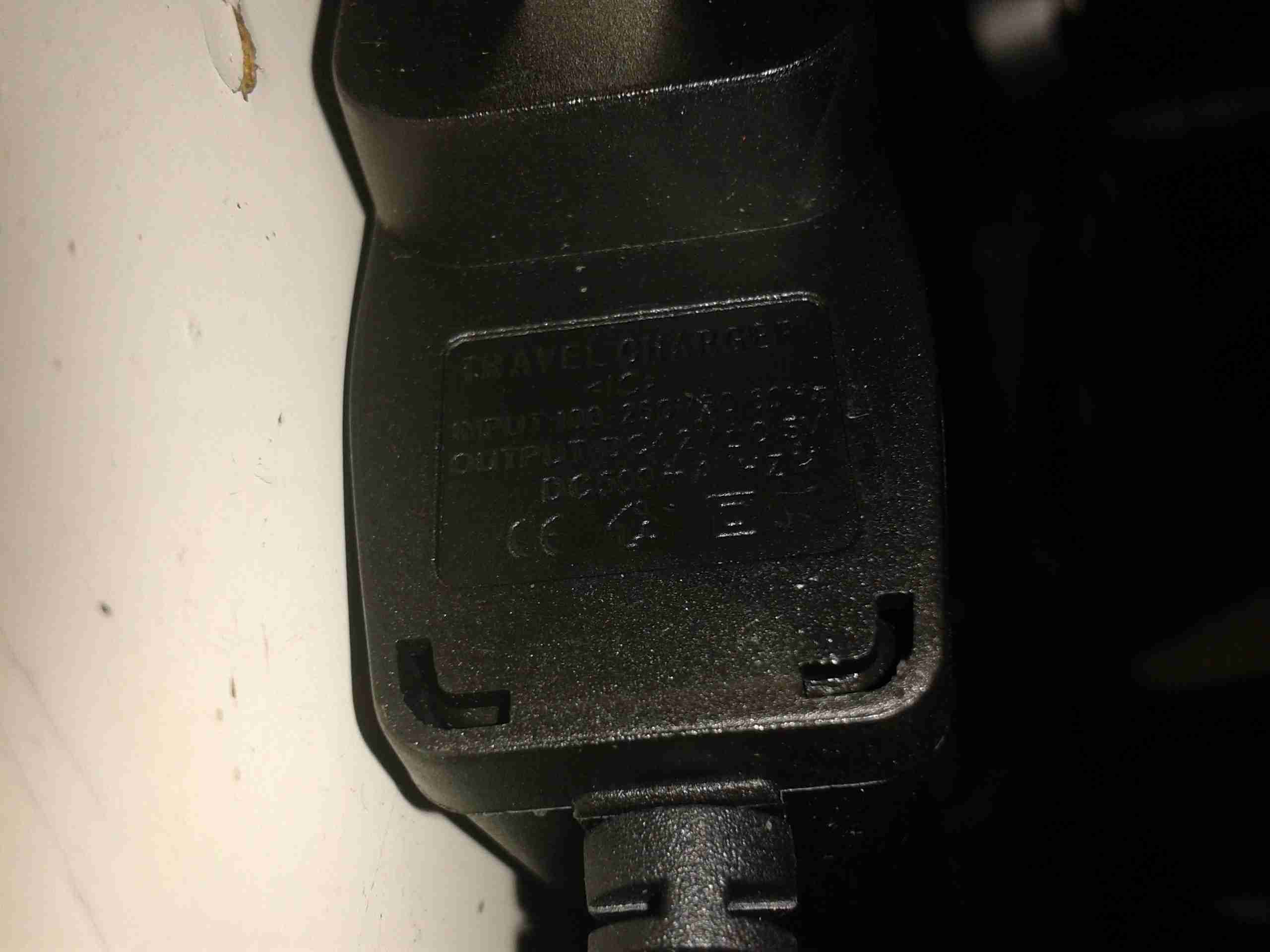
Claimed specifications are 100-240v AC input, making it universal, and 4.2v DC out ±0.5v at 500mA.
Considering the size of the output wire, if this can actually output rated voltage at rated current I’ll be surprised.
Opened
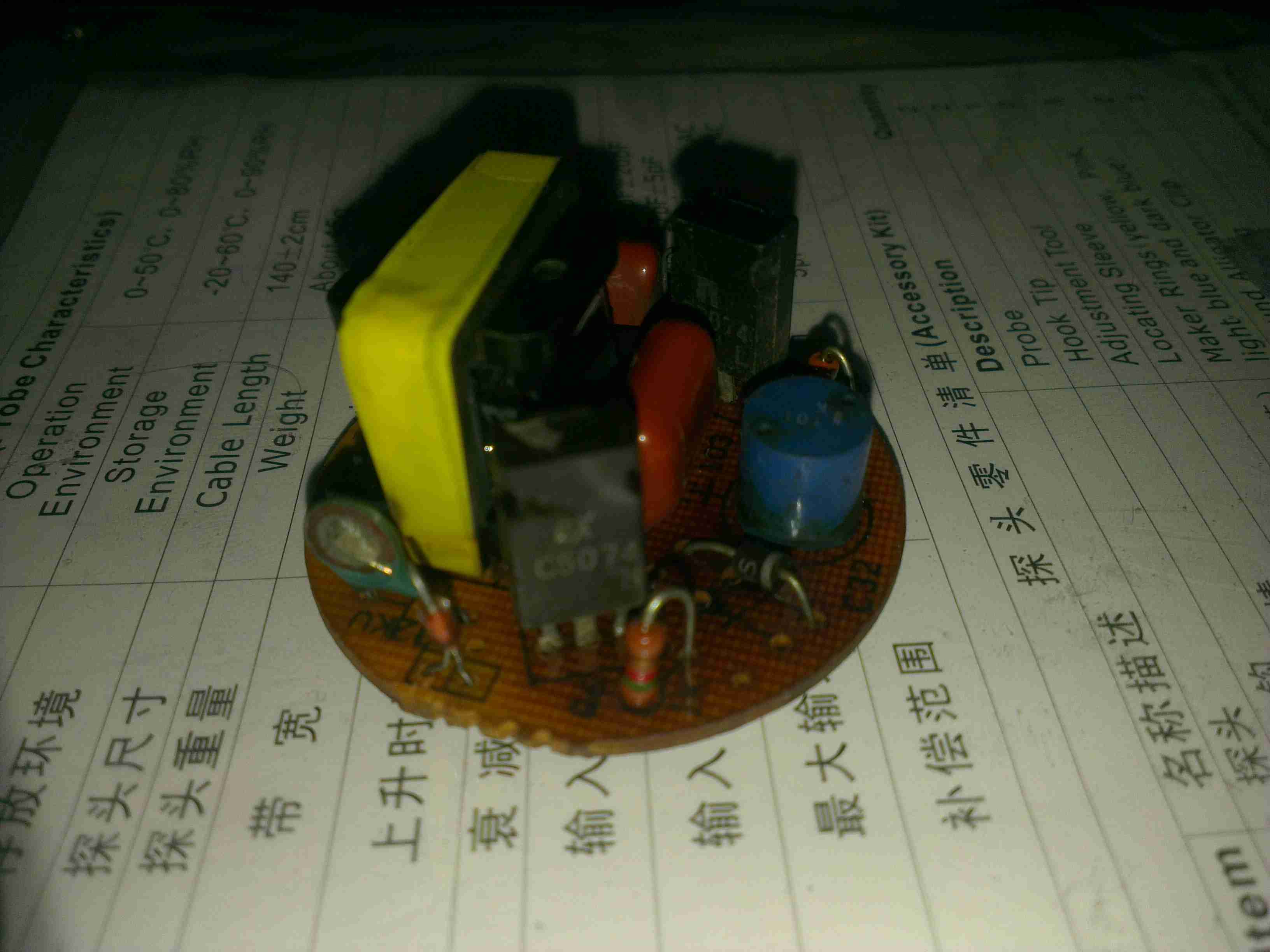
Here’s the adaptor opened up. There’s no mains wiring to speak of, the mains pins simply push into tags on the PCB.
PCB Top
Top of the SMPS PCB. As usual with Chinese gear, it’s very simple, very cheap and likely very dangerous. There’s no real fusing on the mains input, only half-wave rectification & no EMI filtering.
PCB Bottom
Here’s the bottom of the PCB. At least there’s a fairly sized gap between the mains & the output for isolation. The wiggly bit of track next to one of the mains input tags is supposed to be a fuse – I somehow doubt that it has the required breaking characteristics to actually pass any safety standards. Obviously a proper fuse or fusible resistor was far too expensive for these.
The output wiring on the left is thinner than hair, I’d say at least 28AWG, and probably can’t carry 500mA without suffering extreme volt drop.
A member of the family recently bought one of these torches from Maplin electronics, and the included chargers for the 18650 lithium-ion cells leave a lot to be desired.
Torch
Here’s what’s supplied. The torch itself is OK – very bright, and a good size. Me being cynical of overpriced Chinese equipment with lithium batteries, I decided to look in the charging base & the cigar-lighter adaptor to see if there was any actual charging logic.
Charger
Answer – nope. Not a single active component in here. It’s just a jack connected to the battery terminals. There’s all the space there to fit a proper charging circuit, but it’s been left out to save money.
OK then, is it inside the cigarette lighter adaptor?
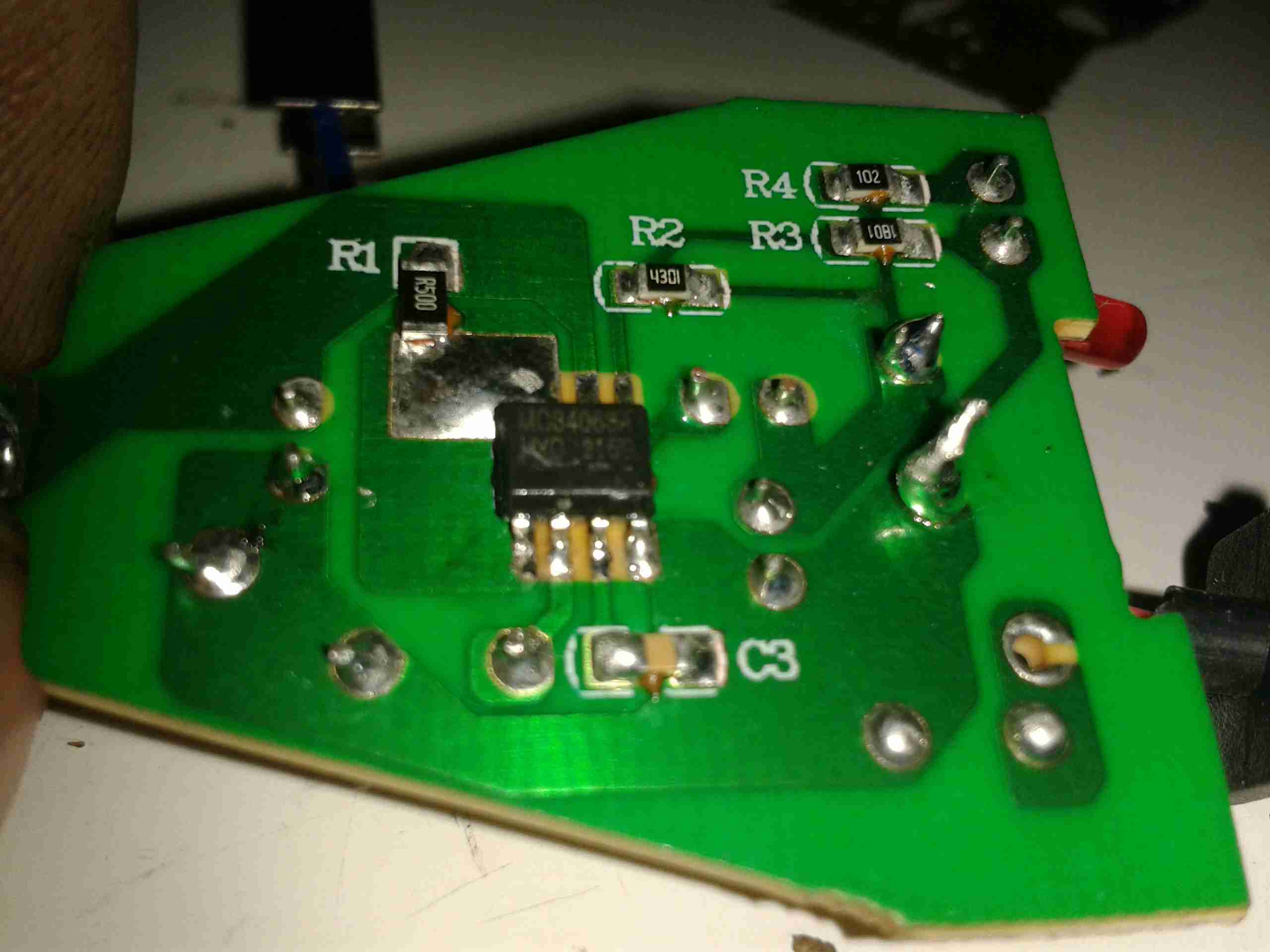
Lighter Adaptor
Nope. Not a single sign of anything resembling a Lithium-Ion charger IC. There’s a standard MC34063A 1.5A Buck converter IC on the bottom of the PCB, this is what’s giving the low voltage output for the torch.
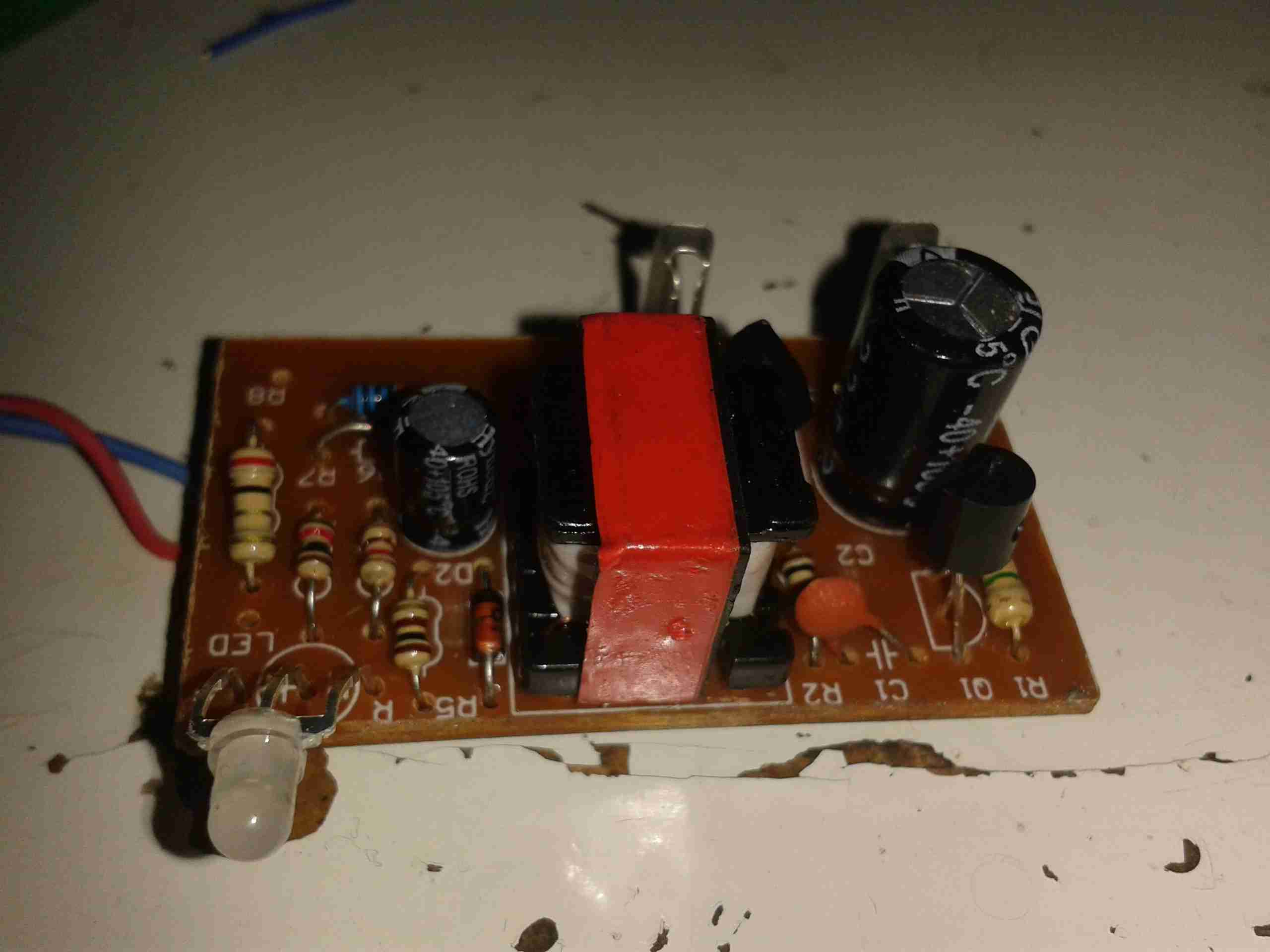
Charger Bottom
Here’s the IC – just a buck converter. The output voltage here is 4.3v. This is higher than the safe charging voltage of a lithium ion cell, of 4.2v.
The cells supplied are “protected” versions, having charge/discharge protection circuitry built onto the end of the cell on a small PCB, this makes the cell slightly longer than a bare 18650, so it’s easy to tell them apart.
The manufacturers in this case are relying on that protection circuit on the cell to prevent an overcharge condition – this isn’t the purpose they’re designed for, and charging this way is very stressful for the cells. I wouldn’t like to leave one of these units charging unattended, as a battery explosion might result.
More to come shortly when I build a proper charger for this torch, so it can be recharged without fearing an alkali metal fire!
I’m still on my crusade of removing every trace of 240v mains power from my shack, so next up are my computer monitors.
I have 4 Dell monitors, of various models, hooked up to my main PC.
The monitor here is a Dell E207WFPc 20″ widescreen model. There will be more when I manage to get the others apart to do the conversion. However I’m hoping that the PSU boards are mostly the same.
Panel Removed
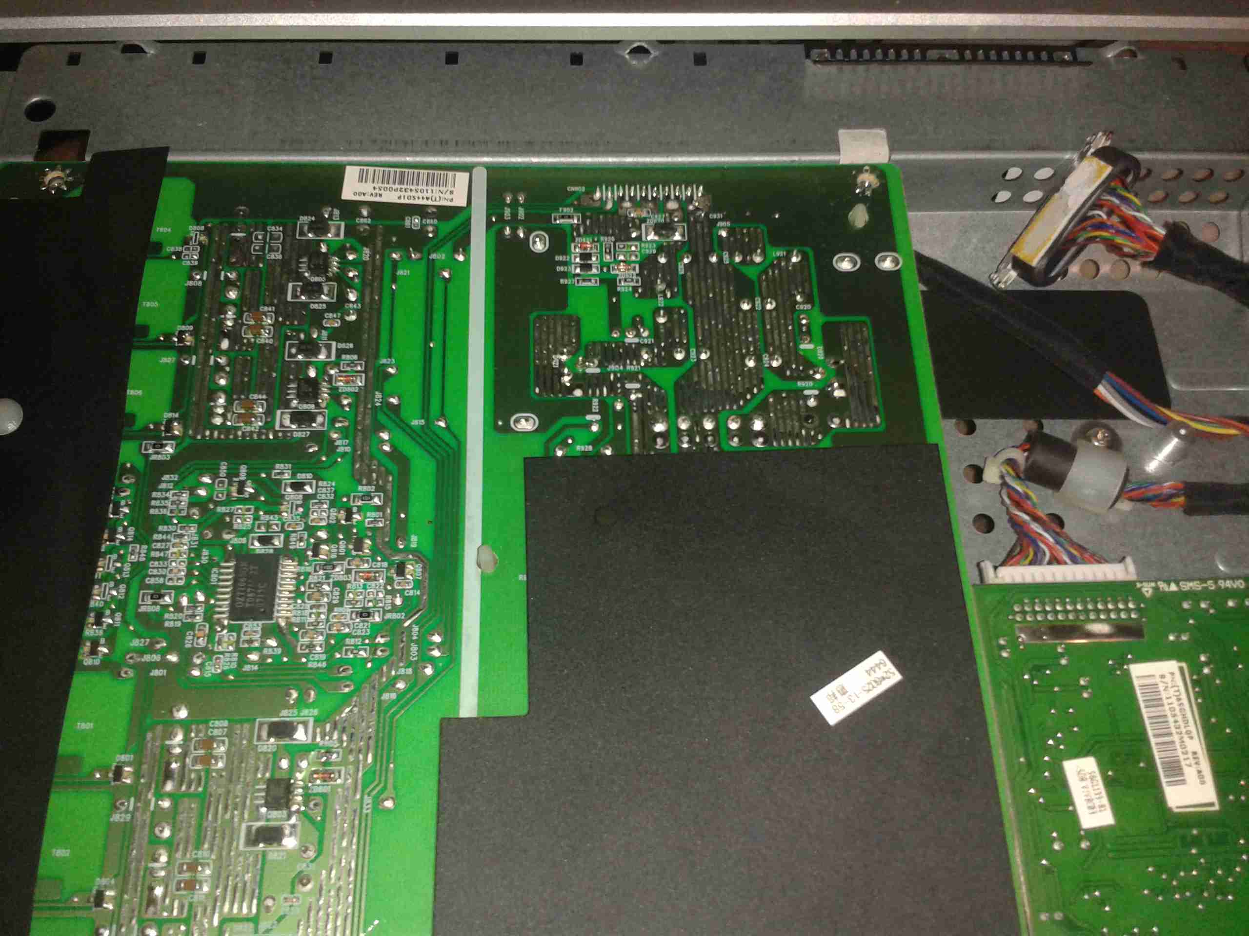
There are no screws holding these monitors together, the front bezel is simply clicked into place in the back casing, these clips are the only thing that holds the relatively heavy glass LCD panel & it’s supporting frame! The image above shows the panel removed. The large board on the left is the power supply & backlight inverter, the smaller one on the right is the interface board to convert the DVI or VGA to LVDS for the LCD panel itself.
PSU Board
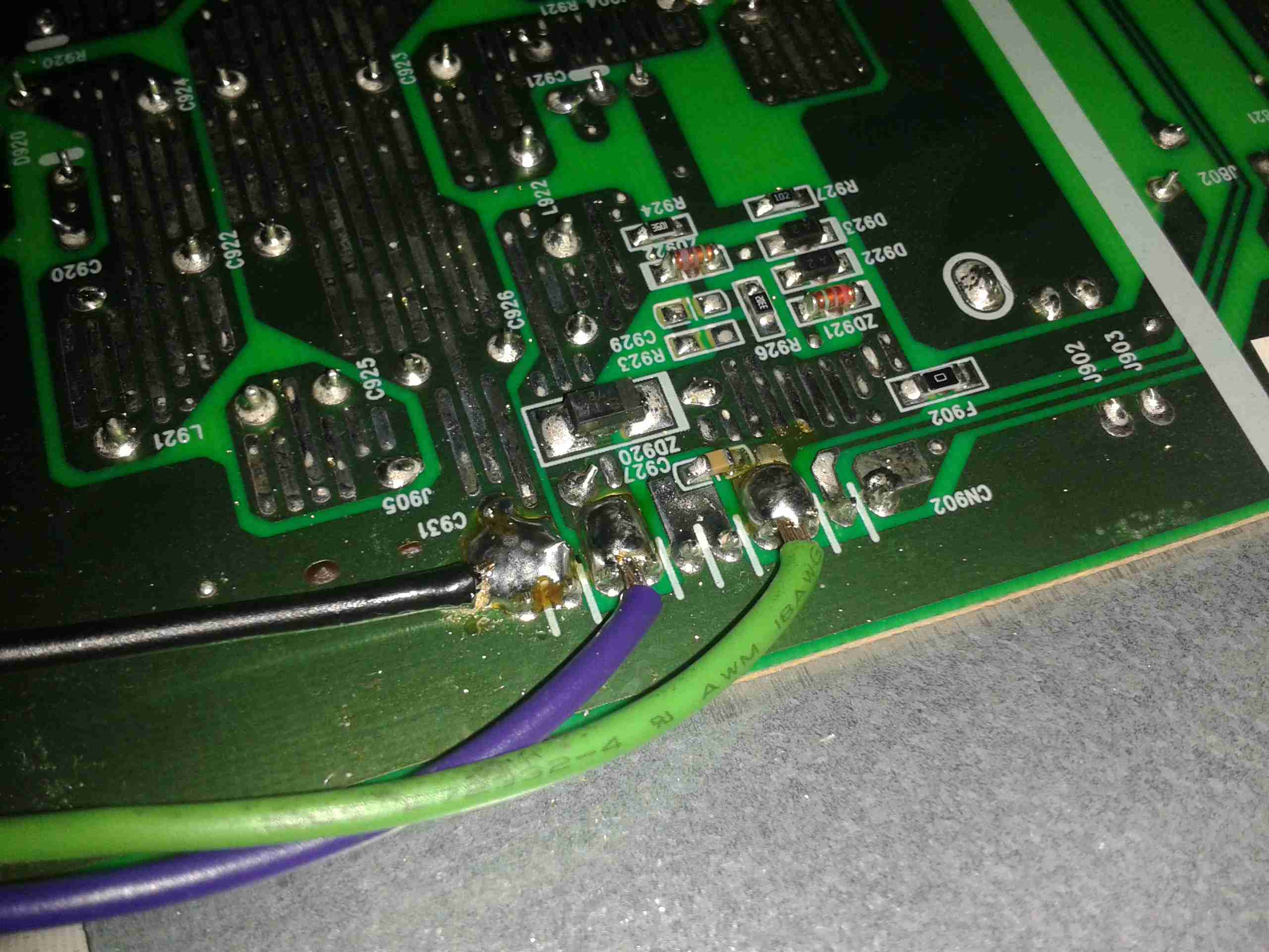
Here’s a closeup of the PSU board, the connector at centre right at the top of the PCB is the main power output, and also has a couple of signals to control the backlight inverter section of the PSU, on the left side. The PSU requirements for this monitor are relatively simple, at 14.5v for the backlight & 5v for the logic board.
PSU
Here’s the top of the PSU board, very simple with the mains supply on the right side, and the backlight inverter transformers on the left.
Hooked In
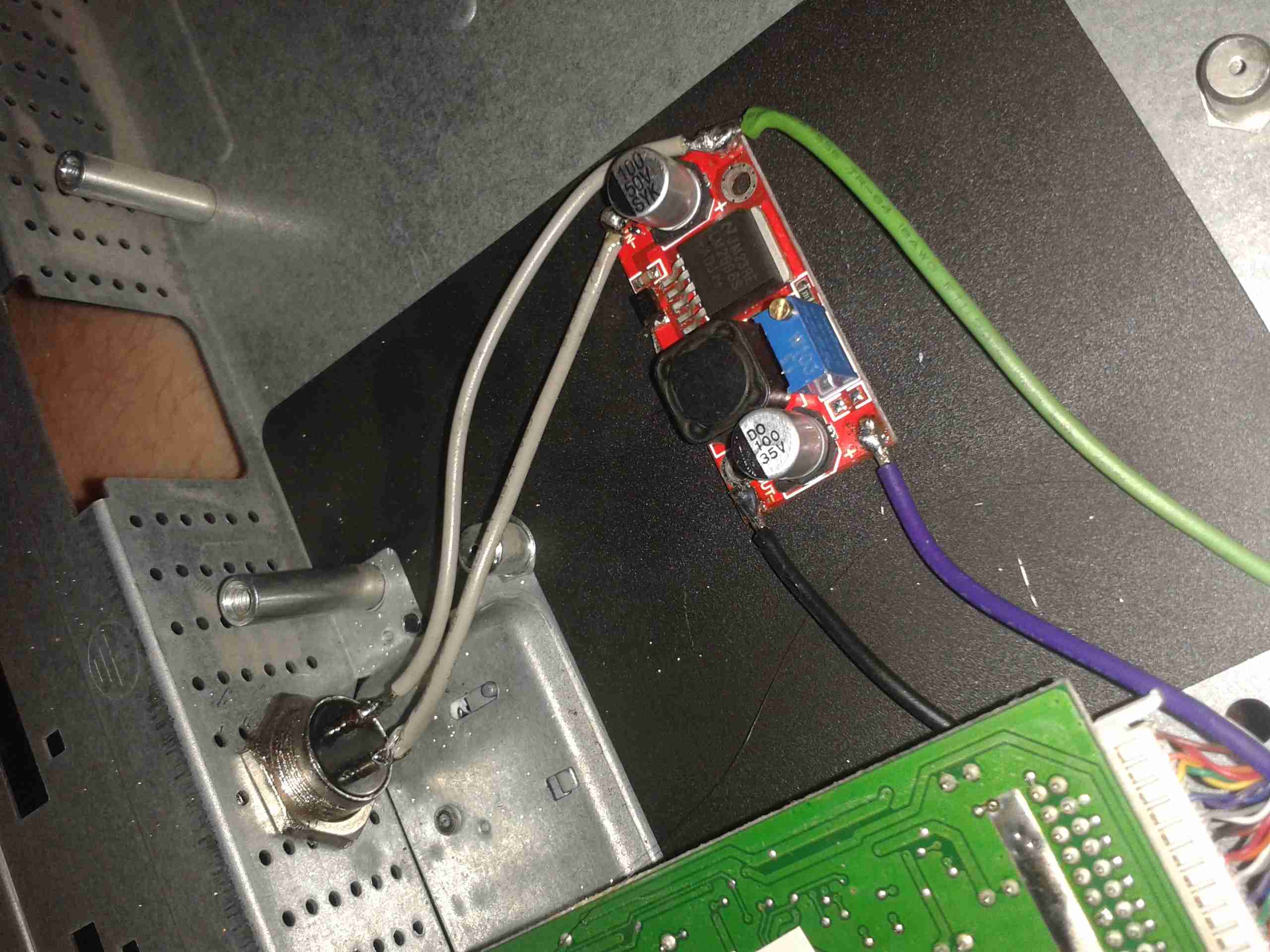
Here I’ve hooked into the power rails on the supply, to attach my own 12v regulators. The green wire is +14.5v, and the purple is +5v. Black is common ground.
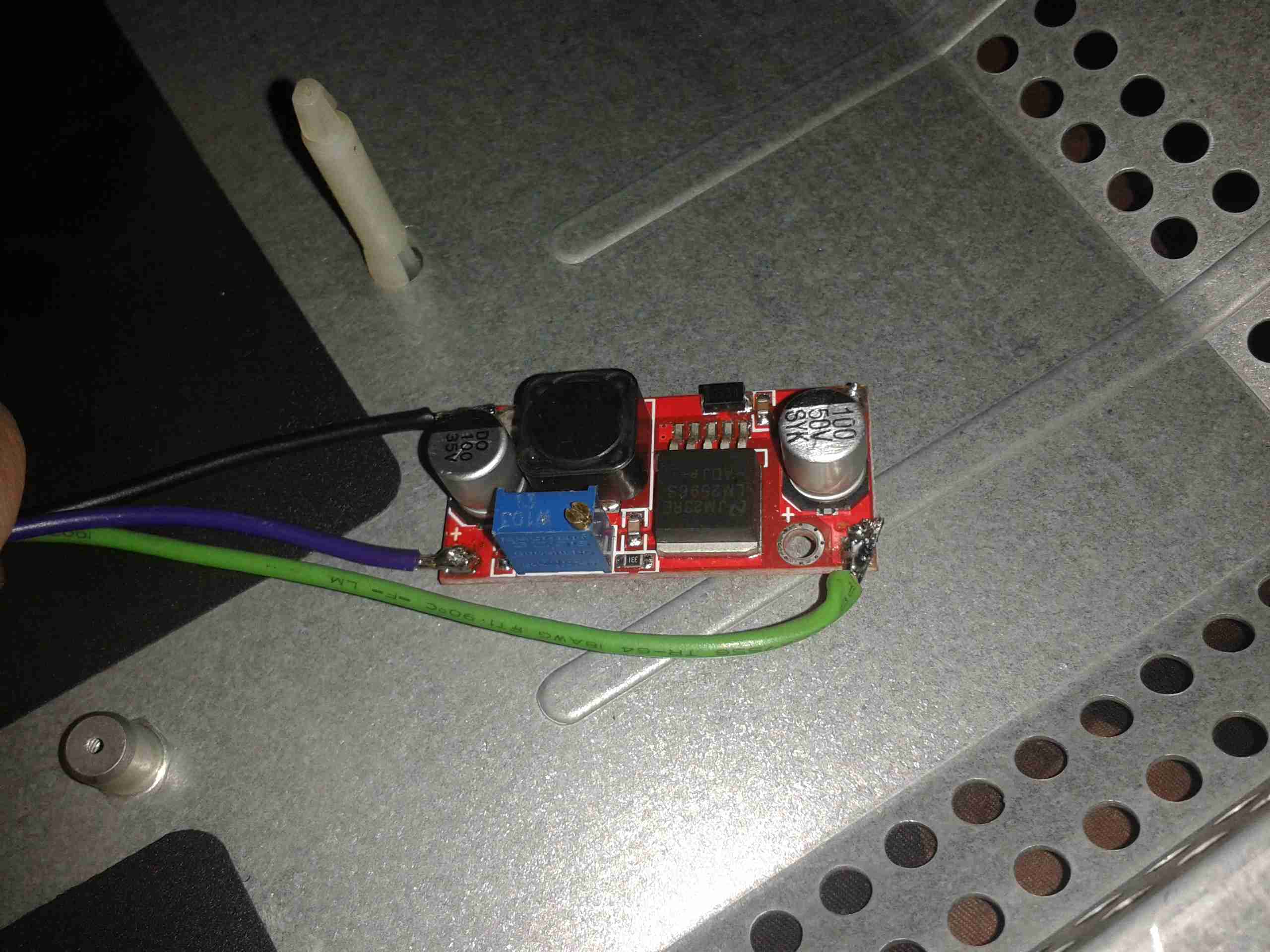
5v Regulator
On doing some testing, the backlight inverter section doesn’t seem to mind voltages between 11.5-14.5v, so a separate regulator isn’t required there. Even running off batteries that’s within the range of both charging & discharging. The only regulator required is a 5v one to reduce the input voltage for the logic PCB.
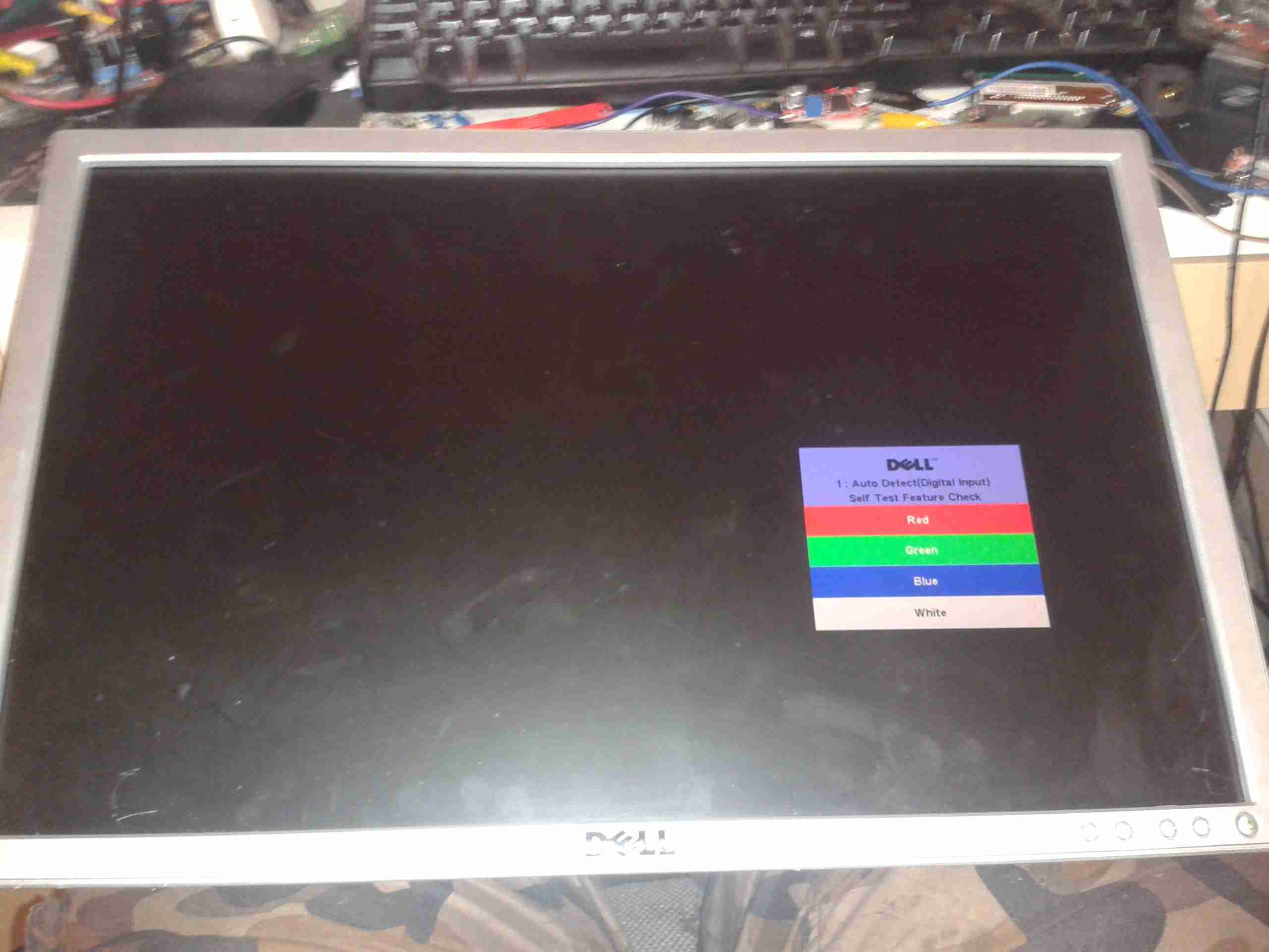
First Test
On applying some 12v power to the regulator input, we have light! Current draw at 12.5v is 2.65A for a power consumption of 33W.
12v Input
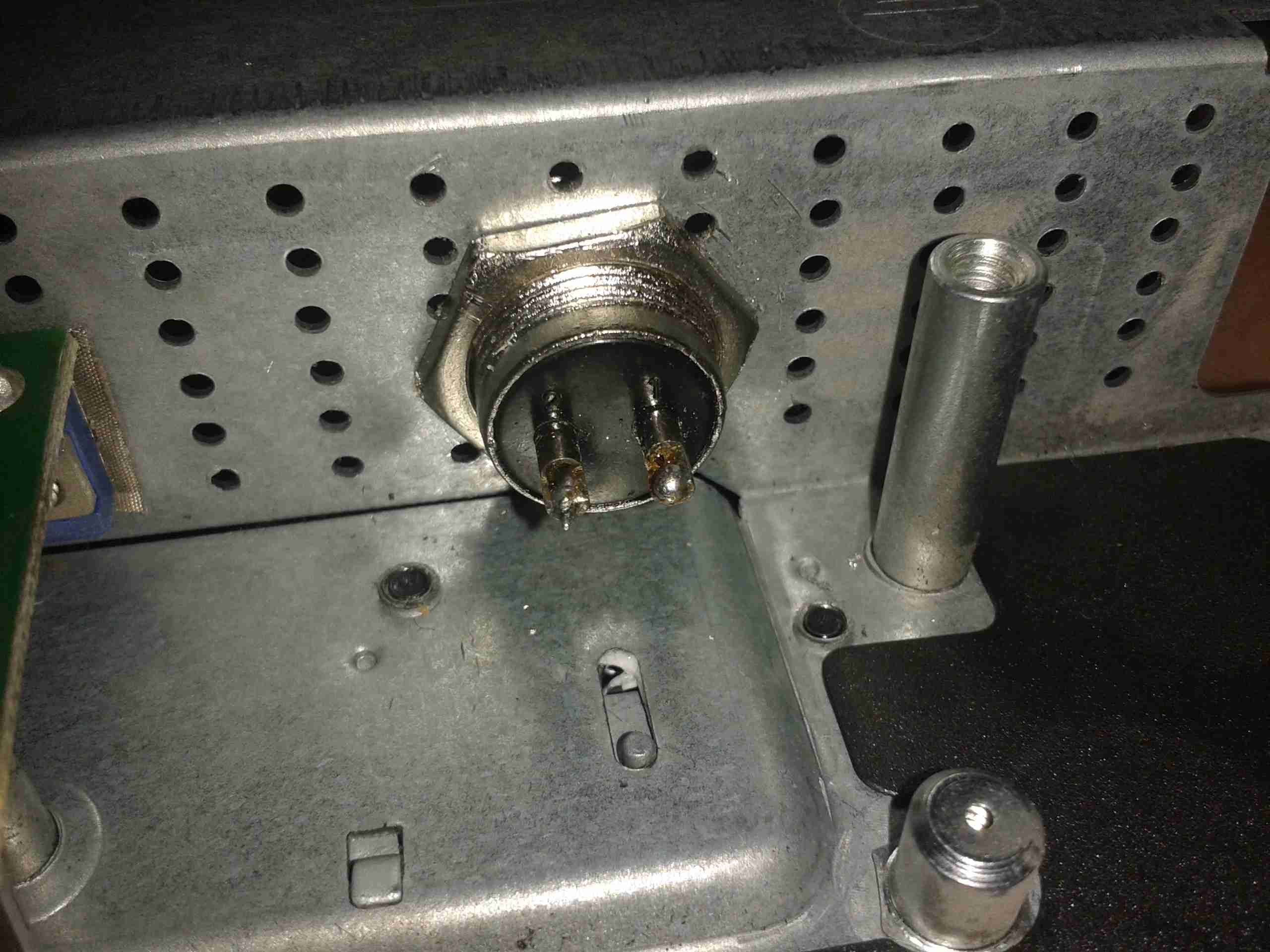
There’s plenty of room in the back casing to mount a 12v input socket, I have left the mains supply intact so it can be used on dual supply.
Final Wiring
Here’s the 5v regulator mounted on the back of the casing, all wired up & ready to go.
This is basically an industrial, rugged MP3 player, in an extruded aluminium case.
They are used in commercial settings for generating telephone hold music or continual playback of background music in shops.
USB1100
It’s quite a compact unit, in a nice aluminium case, designed for mounting into a comms setup. This unit will play any MP3 file, up to a maximum size of 11MB.
Connections
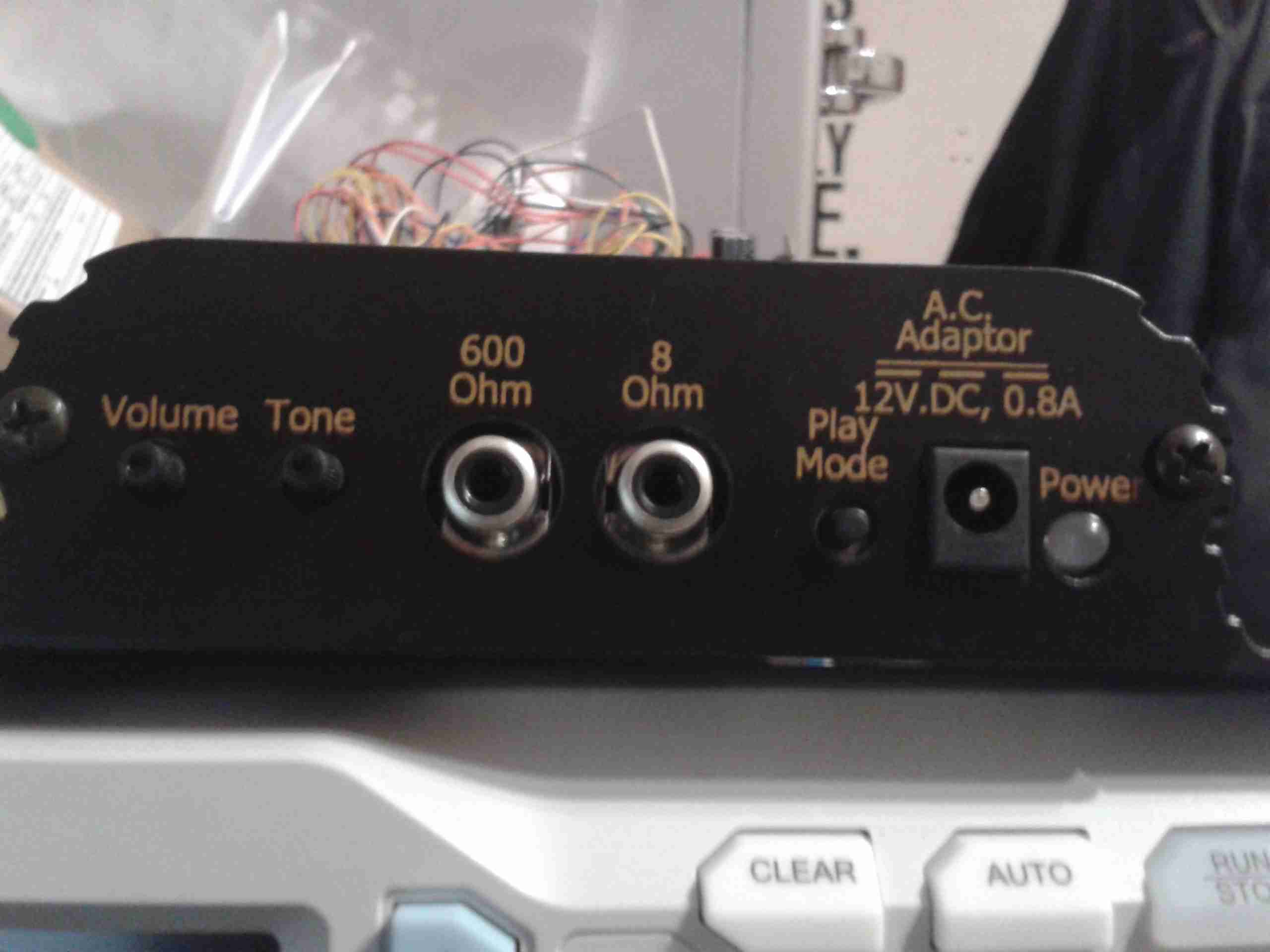
Here’s the user connections on the end of the unit. The device takes a standard 12v DC input, and has a single button for setup, user feedback is given through the multi-colour LED next to the power jack.
Both 8Ω & 600Ω audio outputs are provided for maximum compatibility. Volume & tone controls are also here.
On the other end of the unit is a single USB port for loading the audio files from a USB drive, and a reset button.
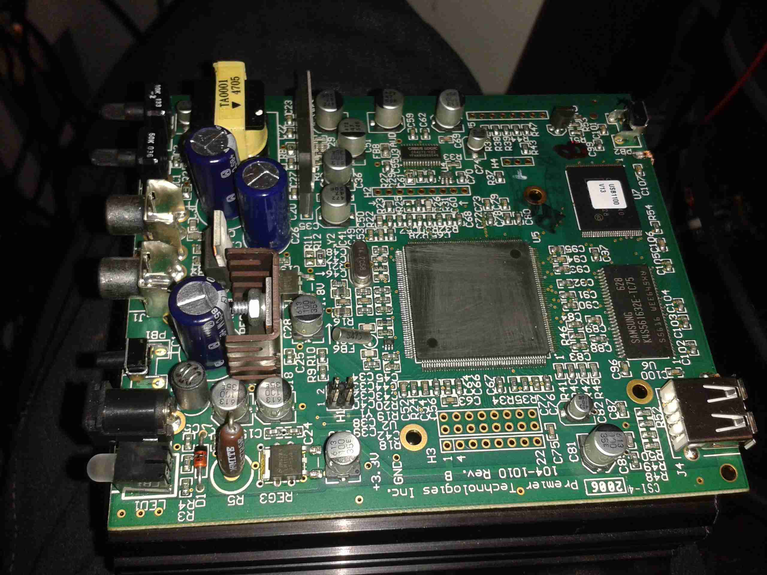
Main PCB
Here’s the single PCB removed from the casing. Unfortunately the main CPU has had it’s part number sanded off, and I can’t be bothered to try & find out what kind of processor it is at this point. To the right of the CPU are some flash ROM & SDRAM, along with the single USB port at bottom right.
The left side of the board is dedicated to audio output & voltage regulation, there are a fair few linear regulators in this unit.
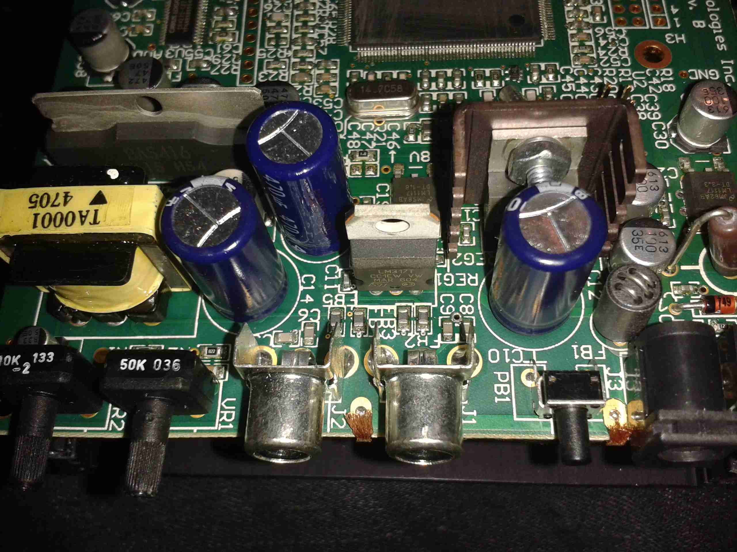
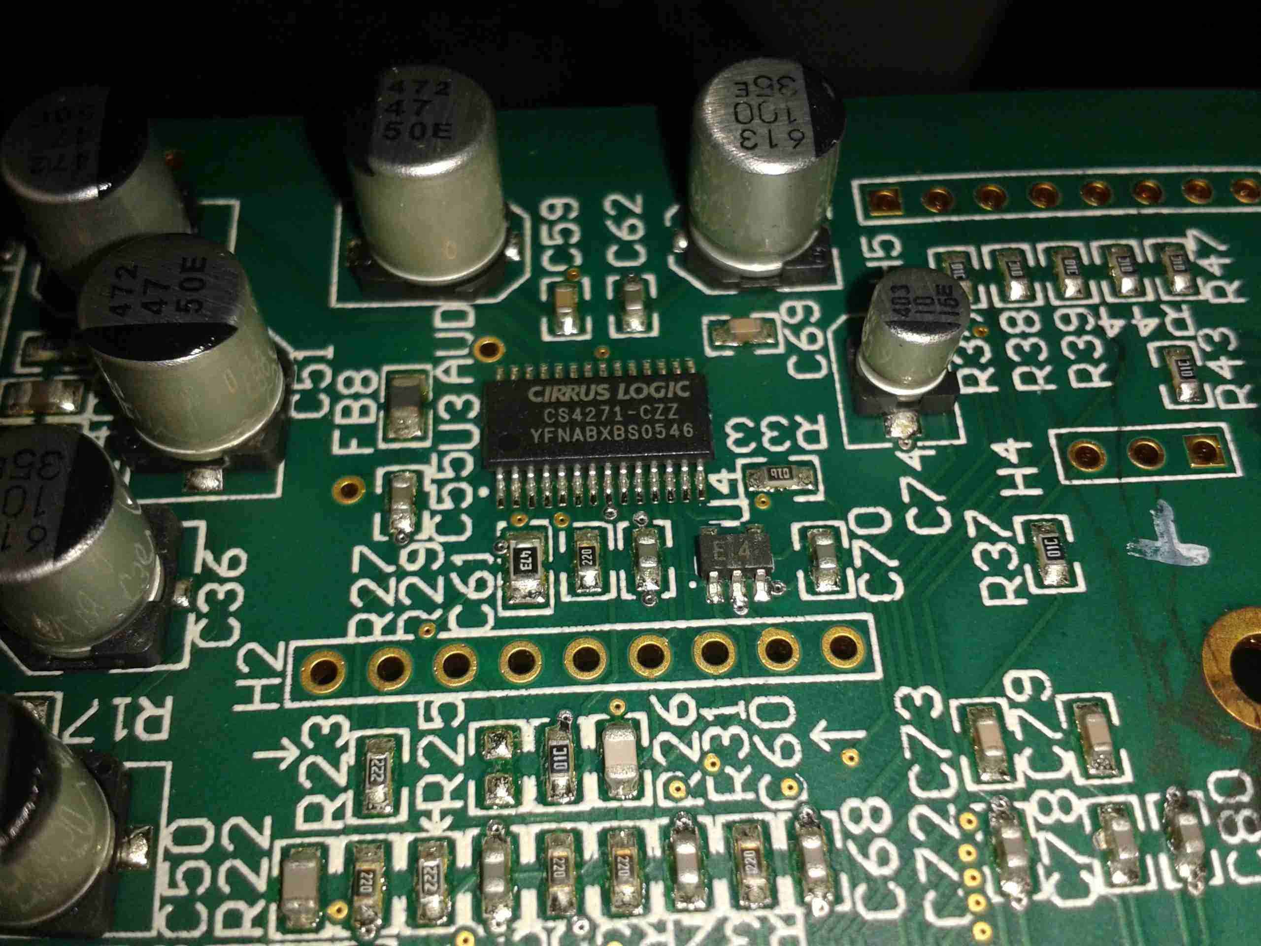
Audio End
Here’s the audio output side of the board, the transformer on the left is to provide the 600Ω output, the audio amplifier IC (BA5416) is just behind it. To the right are some of the main voltage regulators, a 5v one on the heatsink & a LM317.
Audio Codec
The audio codec is a CS4271 from Cirrus Logic, a really high quality part, 24-bit resolution, 192kHz Stereo codec. Considering this is for telephone & PA systems that aren’t that high fidelity, it’s well built!
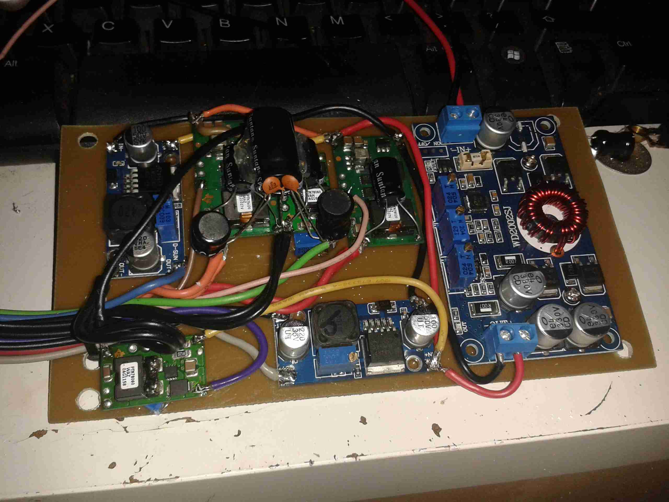
All of the parts I required to complete the supply arrived this morning. After several hours of building, here’s what I came up with:
12v Power Supply
I’ve mounted everything on a piece of FR4 PCB, with it’s copper plane grounded to the case. This backing board is the same size as the original PSU PCB to allow it to be screwed into the same location in the scope.
The power comes in via the converter on the right, which outputs a single 24v rail for the rest of the supplies. The other 6 supplies then generate the individual voltage rails that the scope requires. The use of a single input supply allows this system to operate at voltages up to 30v DC, so it’s good for both 12v & 24v systems.
Scope Ripple
At present the only issue is with some ripple on one of the supplies, this is showing up on the scope display with no input connected at the lowest volts/division. Parts are on order from Farnell to build some common mode filters to remove this from the DC output.
On a 13.8v supply, the scope draws about 1.5A total from the supply, giving a total power consumption of 20.7W. This is with all 4 channels enabled.
My wiring assignments & DC-DC converter ratings are in the table below
Connector Pin
PCB Pin
Signal
Mainboard
DC-DC Rating
Wire Colour
1
10
GND
GND
N/A
BLACK
2
2
+9v_GND
FAN --
NA
BLACK
3
8
+7.5V
6.3V
6A
ORANGE
4
14
-7.5V
-7.5V
2A
GREEN
5
1
NOT USED
AC_TRIG
N/A
NOT USED
6
4
+5V
5V5A
6A
RED
7
6
GND
GND
N/A
BLACK
8
7
GND
GND
N/A
BLACK
9
12
-17.5V
-17.5V
3A
PURPLE
10
9
+7.5V
6.3V
6A
ORANGE
11
3
+9V
FAN +
1A
GREY
12
11
17.5V
17.5V
3A
BLUE
13
5
+5V
5V5A
6A
RED
14
13
GND
GND
N/A
BLACK
Stay tuned for the final section of this build with the power supply filtering & main DC input connections!
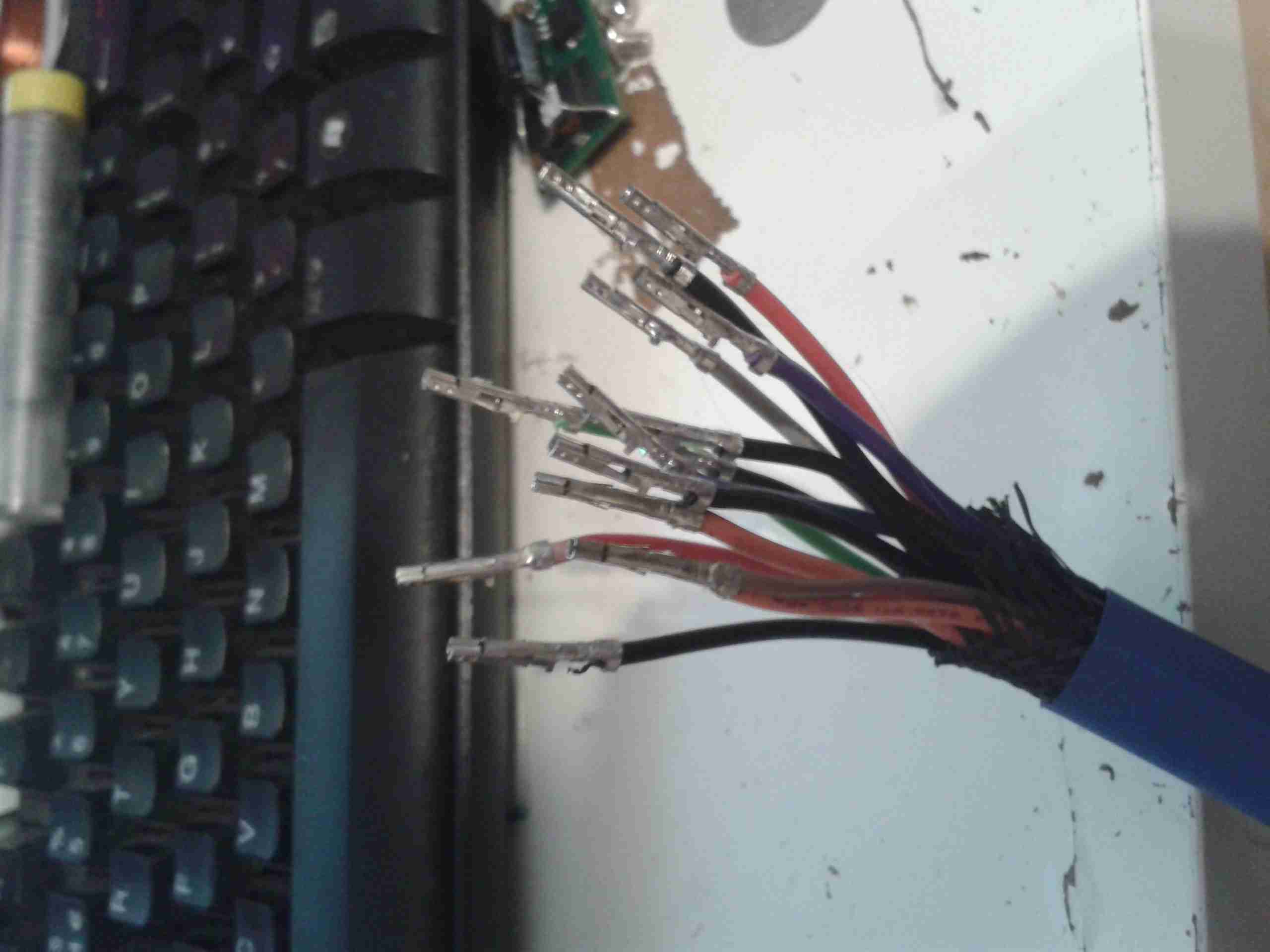
As the crimp tool for the PSU connector in the Rigol scope is a very expensive piece of hardware, I decided to use pre-crimped terminals, from an ATX power connector. (They’re the same type).
Wiring Loom
Here’s the partially completed loom, with the 13 cores for the power rails. The 14th pin is left out as that is for AC triggering, and this won’t be usable on a low voltage supply.
A couple of the pins have two wires, this is for voltage sensing at the connector to compensate for any voltage drop across the cable. The regulators I am using have provision for this feature.
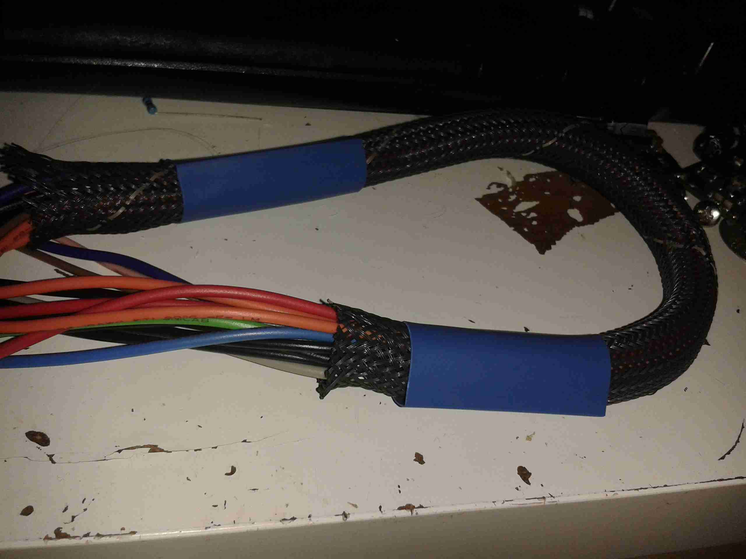
Sleeving
To keep the wiring tidy, I dug a piece of braided loom sleeving out of the parts bin, this will be finished off with the heatshrink once the pins are inserted into the connector shell.
The remaining parts for the loom have been ordered from Farnell & I expect delivery tomorrow.
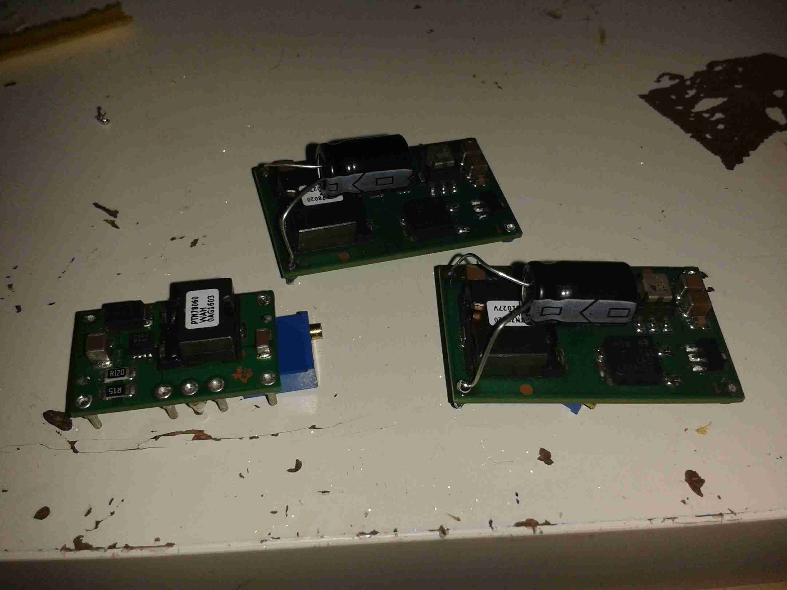
While searching around for regulators to convert my new scope to 12v power, I remembered I had some DC-DC modules from Texas Instruments that I’d got a while ago. Luckily a couple of these are inverting controllers, that will go down to -15v DC at 15W/3A capacity.
I’ve had to order a new module from TI to do the -17v rail, but in the meantime I’ve been getting the other regulators set up & ready to go.
The DC-DC module I’ve got for the -7.5v rail is the PTN78060A type, and the +7.5v & +5v rails will be provided by the PTN78020W 6A buck regulators.
These regulators are rated well above what the scope actually draws, so I shouldn’t have any issues with power.
DC-DC Modules
Here’s the regulators for the 5v, 7.5v & -7.5v rails, with multiturn potentiometers attached for setting the voltage output accurately. I’ve also attached a couple of electrolytics on the output for some more filtering. I’ll add on some more LC filters on the output to keep the noise down to an absolute minimum. These are set up ready with the exact same output voltage as the existing mains AC switching supply, when the final regulator arrives from TI I will put everything together & get some proper rail readings.
There won’t be a proper PCB for this, as I don’t have the parts in Eagle CAD, and I simply don’t have the energy to draw them out from the datasheets.
Since everything in my shack is run from 12v, I thought it would be handy to convert my new scope to 12v as well, as 99% of the places I find myself needing test gear are off grid, with no access to mains supplies.
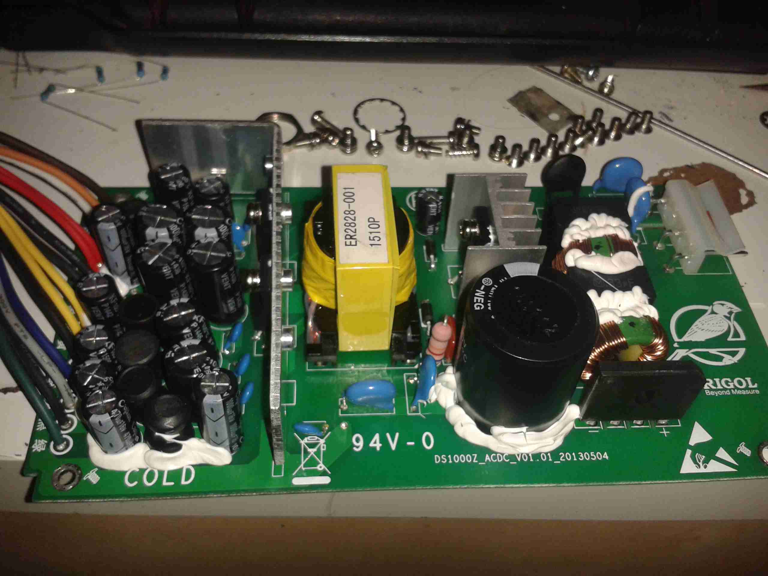
Mains PSU
Here’s the factory mains SMPS unit from the back of the scope. This is a nice multi-rail unit, with several different outputs, the table below details the wiring of the PSU.
Connector Pin
PCB Pin
Signal
Measured Voltage
Mainboard
Rectifier Rating
Wire Colour
5
1
AC_TRIG
N/A
AC_TRIG
N/A
BROWN
2
2
+9v_GND
N/A
FAN --
NA
ORANGE
11
3
+9V
10.16V
FAN +
2A
WHITE
6
4
+5V
5.1V
5V5A
20A
RED
13
5
+5V
5.1V
5V5A
20A
RED
7
6
GND
N/A
GND
N/A
BLACK
8
7
GND
N/A
GND
N/A
BLACK
3
8
+7.5V
6.9V
6.3V
20A
YELLOW
10
9
+7.5V
6.9V
6.3V
20A
YELLOW
1
10
GND
N/A
GND
N/A
BLACK
12
11
17.5V
17.51V
17.5V
2A
BLUE
9
12
-17.5V
-17.36V
-17.5V
2A
GREY
14
13
GND
N/A
GND
N/A
BLACK
4
14
-7.5V
-6.84V
-7.5V
2A
GREEN
The only feature I will lose if I make this switch is AC line triggering, but I never use that anyway, so it’s not a big issue for me.
Since I have been able to locate the connector, the plan is to design a replacement low voltage supply unit for the scope, with the same footprint as the original AC mains supply. This will allow me to do a direct swap without causing any damage or modifying the original supply.
This method will allow me to swap the 240v supply back into the scope if I ever come to need it.
I’m planning to use the LTC3863 DC-DC Controller from Linear Tech to generate the negative rails, this will go down to -150v on the output, so it’s pretty much perfect to generate them.
PSU Output Side
Here’s the output side of the mains PSU, it has a lot of filtering on the output rails, the two TO220 devices are the output rectifiers for the +5v & +7.5v rails, these are rated at 20A, 60V.
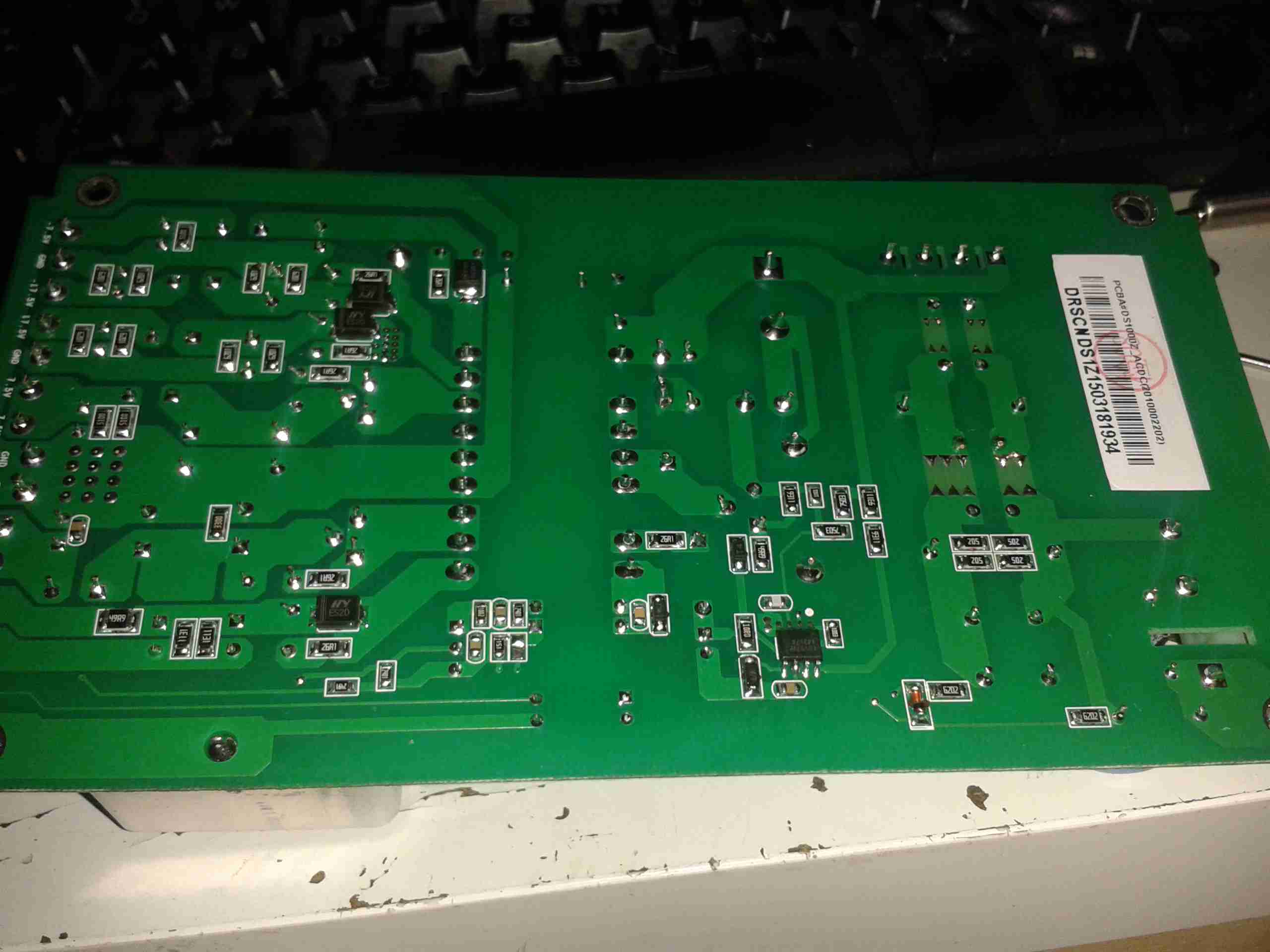
PCB Bottom
Here’s the bottom side of the PCB. It’s a really nicely designed PSU, massive isolation gap, spark gaps on the primary side & good filtering. The output side on the left has the rectifier diodes for the other voltage rails, these are only 2A rated, so designing the inverting supply to generate the negative rails will be pretty easy.
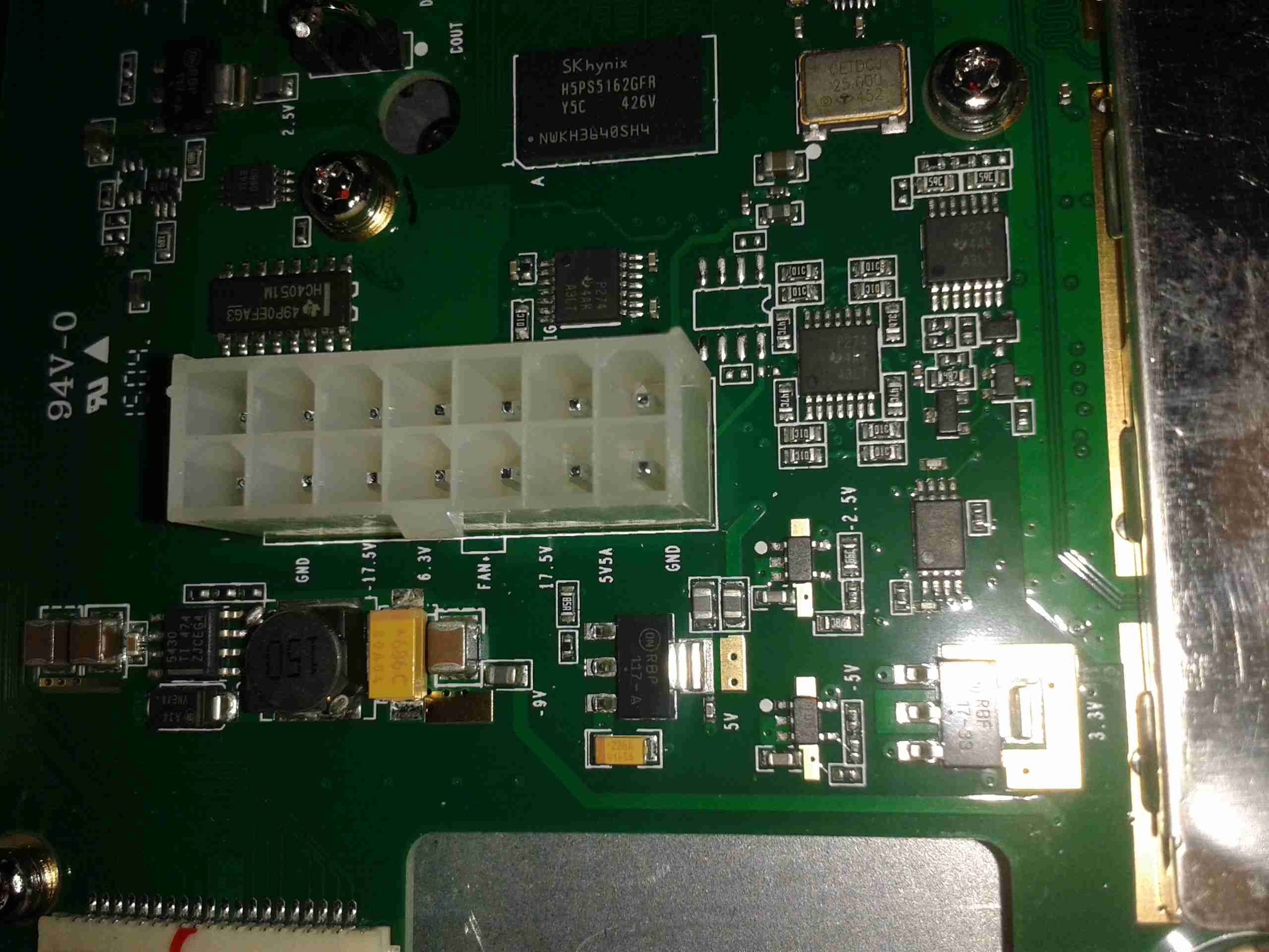
From looking at the PCB markings on both the mainboard & the PSU, the +9v rail seems to be used to drive the fan, both silkscreen markings indicate this.
The voltages marked on the PSU & the mainboard connector don’t quite match up though, there’s a small variation in the stated voltage between the two. This is most likely because all of the regulation of the supplies seems to be done on the mainboard, there are several linear regulators, and a few DC-DC switchers. Providing that the replacement supply isn’t noisy it should work fine.
This is backed up by the fact that the mains PSU only seems to regulate the +5v rail – on measuring the rails that’s the only one that’s close to spec.
Mainboard Power
Here’s the mainboard power connector, with it’s silkscreen labelling on the pins. (Very useful). As can be seen here, there’s at least 5 regulators, of both switching & linear types here, generating both positive & negative rails.
On the boat I have installed custom LED lighting almost everywhere, but we still use CFL bulbs in a standing lamp since they have a wide light angle, and brightness for the size.
I bought a couple of 12v CFLs from China, and the first of these has been running for over a year pretty much constantly without issue. However, recently it stopped working altogether.
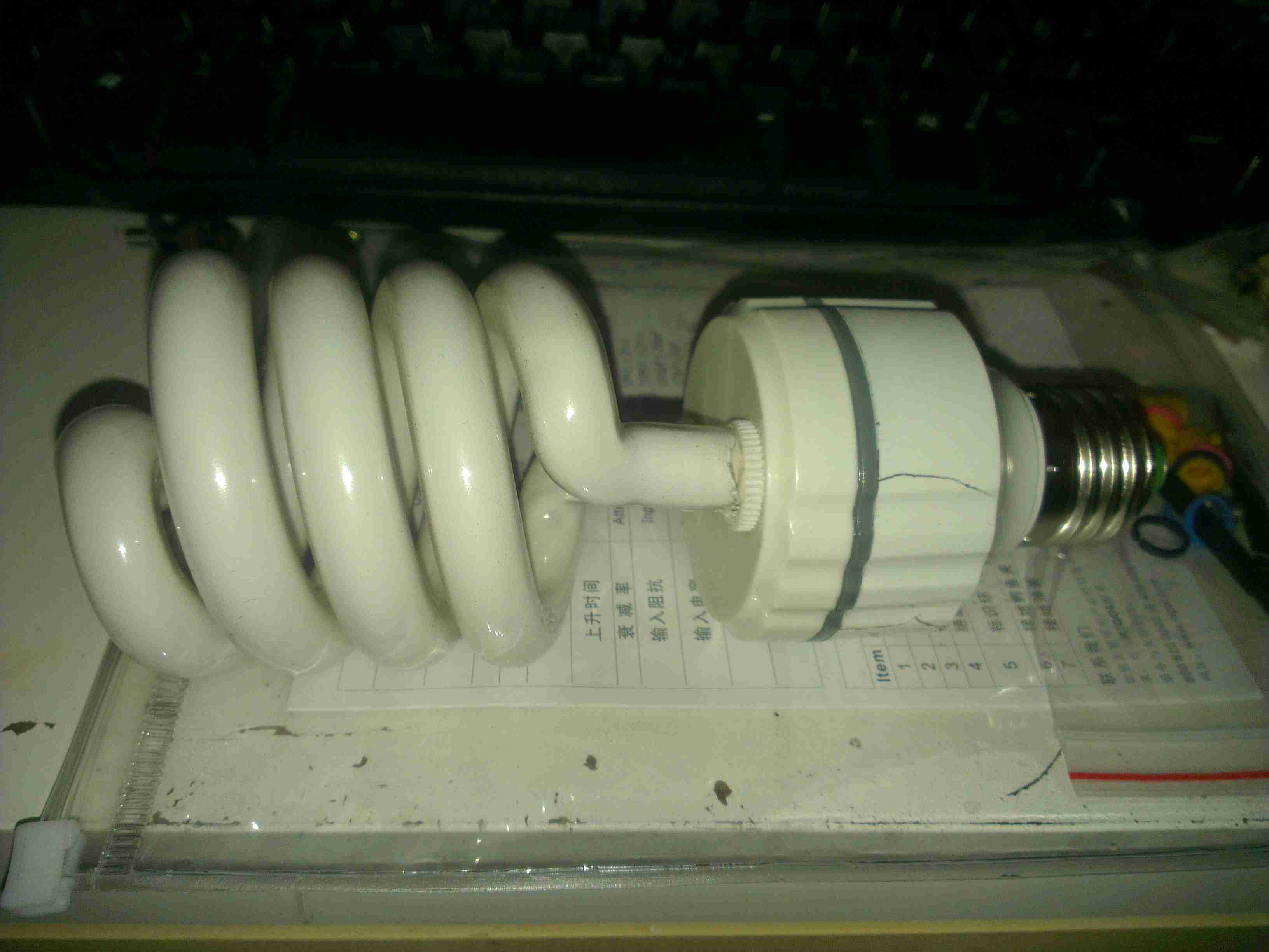
12v CFL
Here’s the lamp, exactly the same as the 240v mains versions, except for the design of the electronic ballast in the base. As can be seen here, the heat from the ballast has degraded the plastic of the base & it’s cracked. The tube itself is still perfectly fine, there are no dark spots around the ends caused by the electrodes sputtering over time.
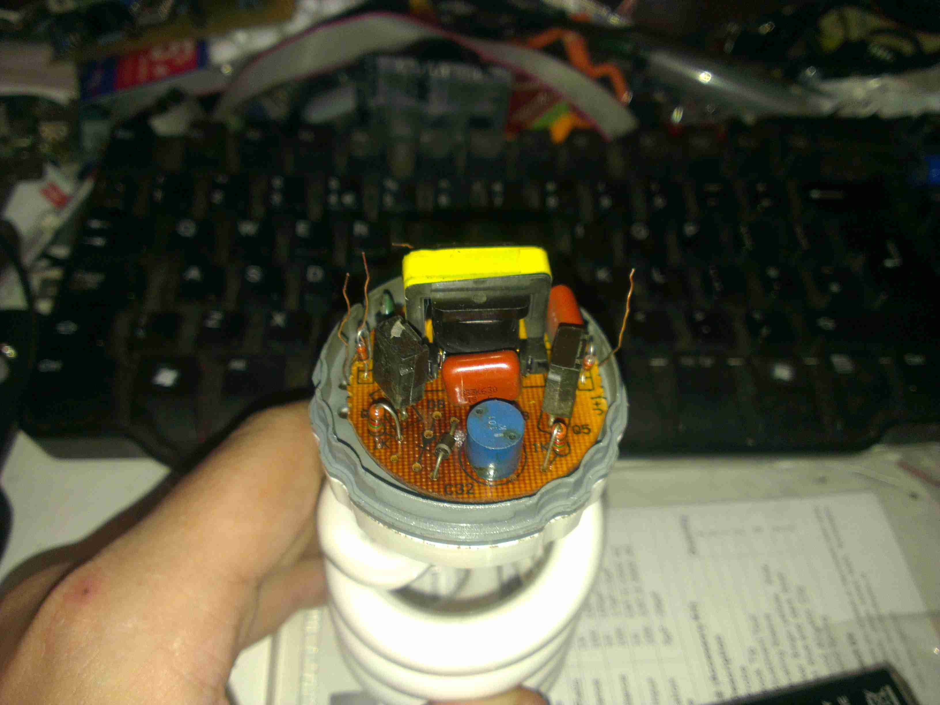
Ballast
Here’s the ballast inside the bottom of the lamp, a simple 2-transistor oscillator & transformer. The board has obviously got a bit warm, it’s very discoloured!
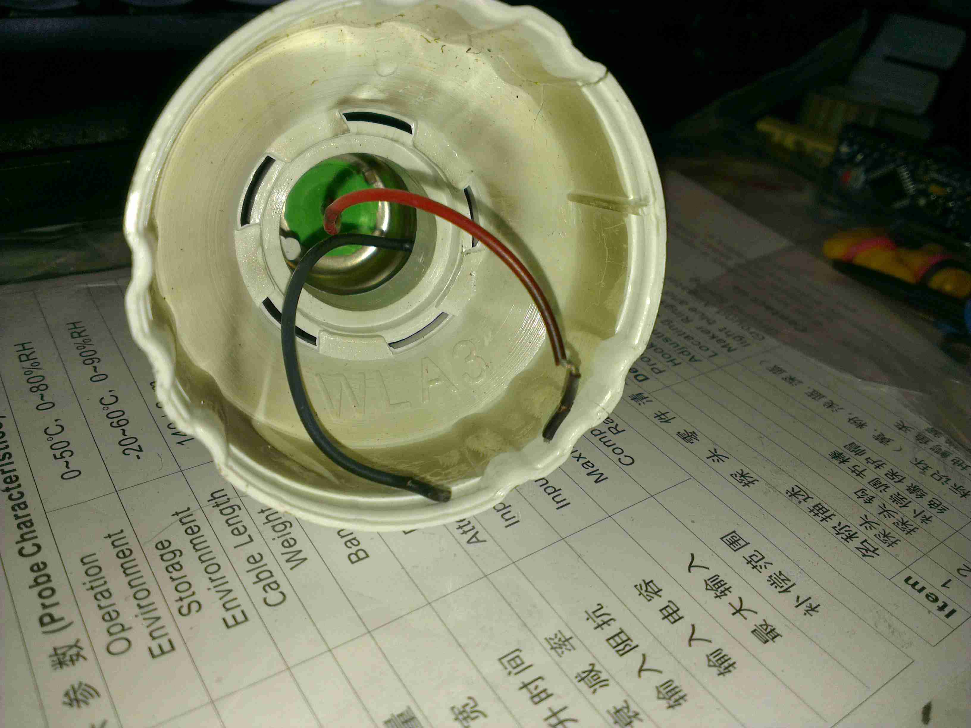
Failed Wiring
The failure mode in this case was cooked wiring to the screw base. The insulation is completely crispy!
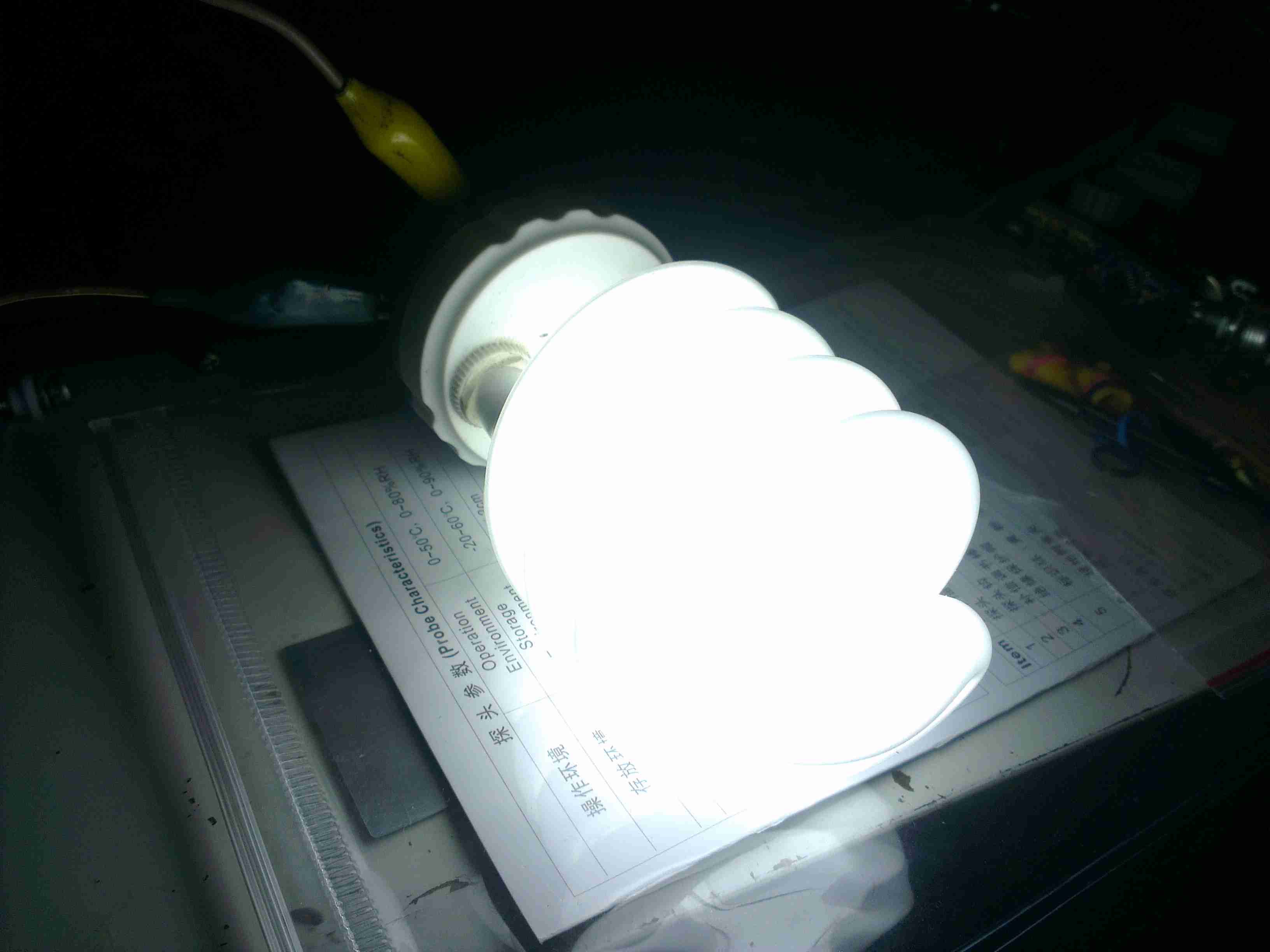
Direct Supply
On connection direct to a 12v supply, the lamp pops into life again! Current draw at 13.8v is 1.5A, giving a power consumption of 20.7W. Most of this energy is obviously being dissipated as heat in the ballast & the tube itself.
Ballast PCB
Here’s the ballast PCB removed from the case. It’s been getting very warm indeed, and the series capacitor on the left has actually cracked! It’s supposed to be 2.2nF, but it reads a bit high at 3nF. It’s a good thing there are no electrolytics in this unit, as they would have exploded long ago. There’s a choke on the DC input, probably to stop RFI, but it doesn’t have much effect.
Supply Waveform
Here’s the waveform coming from the supply, a pretty crusty sinewave at 71.4kHz. The voltage at the tube is much higher than I expected while running, at 428v.
RFI
Holding the scope probe a good 12″ away from the running bulb produces this trace, which is being emitted as RFI. There’s virtually no filtering or shielding in this bulb so this is inevitable.
Having now tested the supply I wrote about in my previous post, I can now say that it’s nameplate rating far exceeds it’s actual capability.
On running the supply under load, at 6.5A the operating frequency drops into the audible range, a big sign of overload. (It makes an irritating continuous chirping noise). The output voltage also drops to 10.5v.
The temperature of the unit while it’s been running under such a load is also questionable, the external casing gets hot enough to cause burns, I haven’t yet been able to stick a thermocouple into the case to see what the internal temperature is.
I’m currently talking with the eBay seller (wwwstation) regarding this, however they are arguing that the supply is only for LEDs & CCTV cameras.
However those two loads are very different, and the supply has no internal regulation for supplying LEDs. As a simple switchmode supply, any load is suitable, providing it’s within the load rating of the supply.
I would estimate that the supply is only capable of 5A as an upper limit.
They are requesting that I return the supply, but I’m yet to find out if they’re going to cover return postage. The item as listed is not as described, and I will escalate things if required.
I will update this post when I hear more back from the eBay seller.
A while ago I blogged about modifying the output voltage of some surplus Cisco switch power supplies to operate at 13.8v.
Since I was able to score a nice Hammond 1598DSGYPBK ABS project box on eBay, I’ve built one of the supplies into a nice bench unit.
Hammond ABS CaseSupply Unit
Above is the supply mounted into the box, I had to slightly trim one edge of the PCB to make everything fit, as it was just a couple of mm too wide. Luckily on the mains side of the board is some space without any copper tracks.
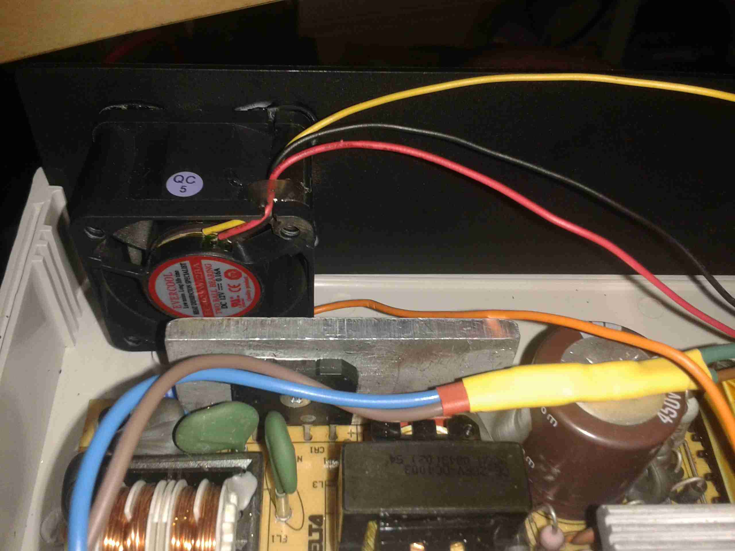
PSU Fan
These supplies are very high quality & very efficient, however they came from equipment that was force-air cooled. Running the PSU in this box with no cooling resulted in overheating. Because of this I have added a small 12v fan to move some air through the case. The unit runs much cooler now. To allow the air to flow straight through the case, I drilled a row of holes under the front edge as vents.
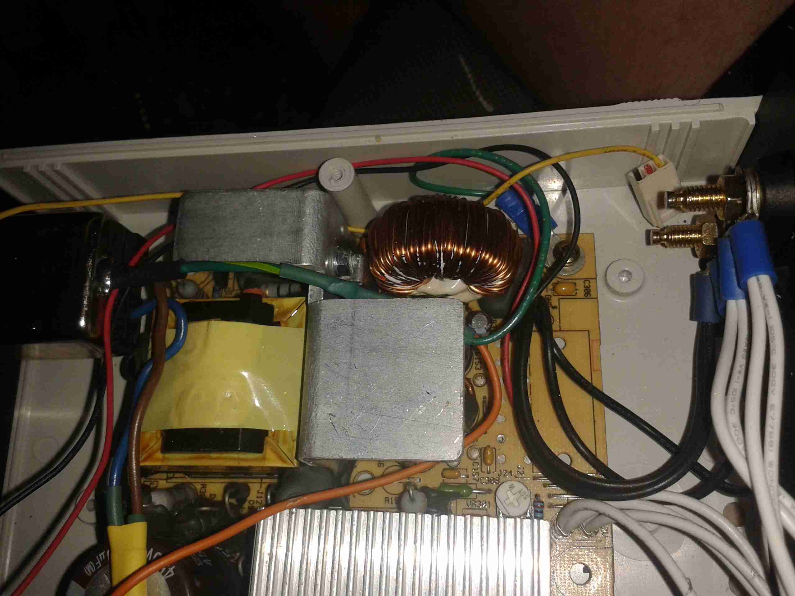
Output Side
Here is the output side of the supply, it uses standard banana jacks for the terminals. I have used crimp terminals here, but they are soldered on instead of crimped to allow for higher current draw. The negative return side of the output is mains earth referenced.
I have tried to measure output ripple on this supply, but with my 10X scope probe, and the scope set to 5mV/Div, the trace barely moves. The output is a very nice & stable DC.
This supply is now running my main radio in the shack, and is small enough to be easily portable when I move my station.
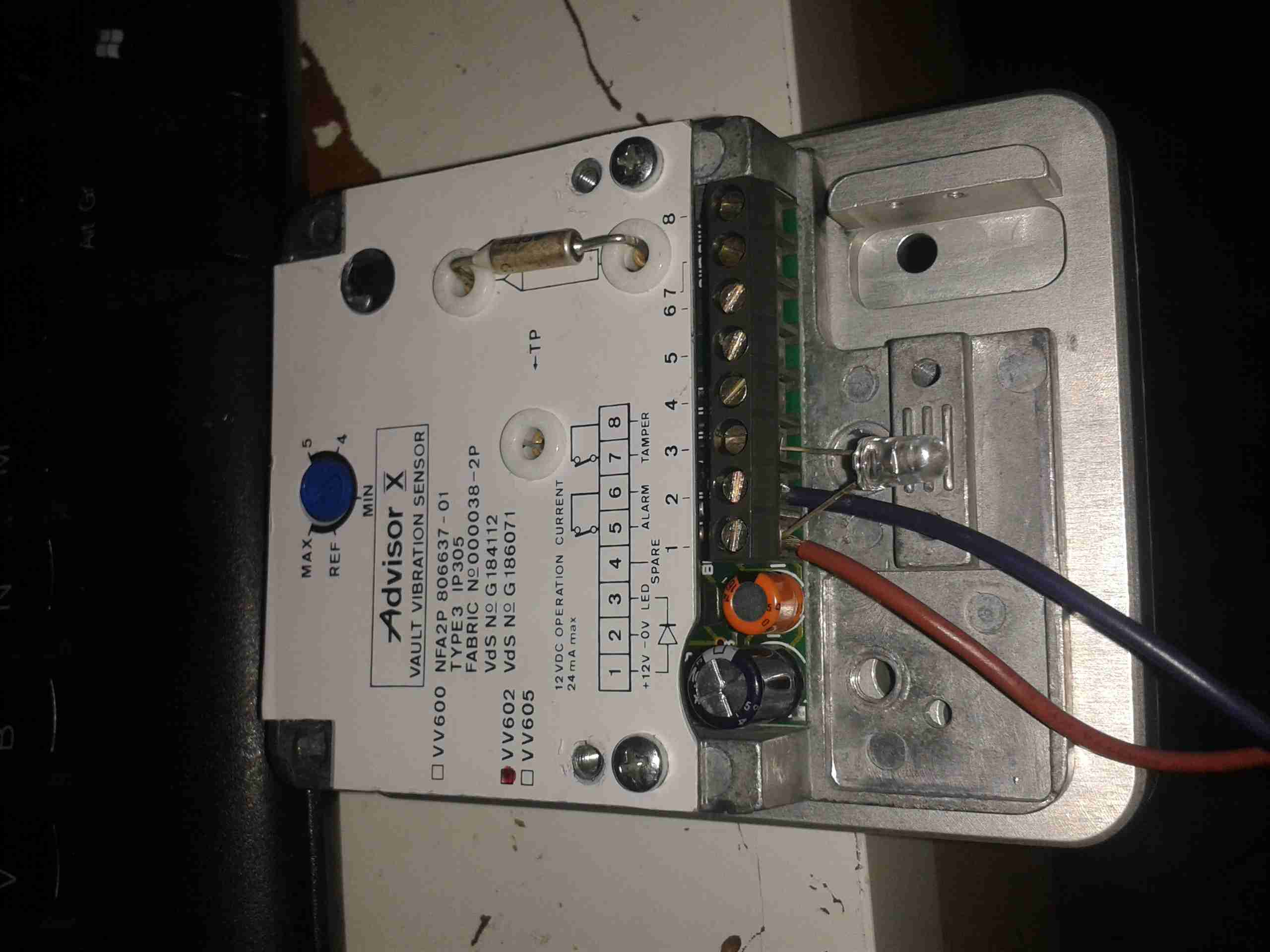
Here’s a rather unique device for protecting safes & vaults from attack by thefts.
It’s an Aritech VV602 seismic detector, based on piezoelectric sensors. Not surprisingly, this unit is covered in tamper sensors as well. There are several different sensor types in use:
Piezoelectric vibration sensing
Thermal sensing
Magnetic sensing
Manual Tamper Switches
Sensor Unit
Above is the main unit, with the thermal sensor. This is just a thermal fuse, very commonly used in everything from room heaters to hairdryers. This one triggers at 84°C. The adjustment pot is also visible here.
Mounting Plate
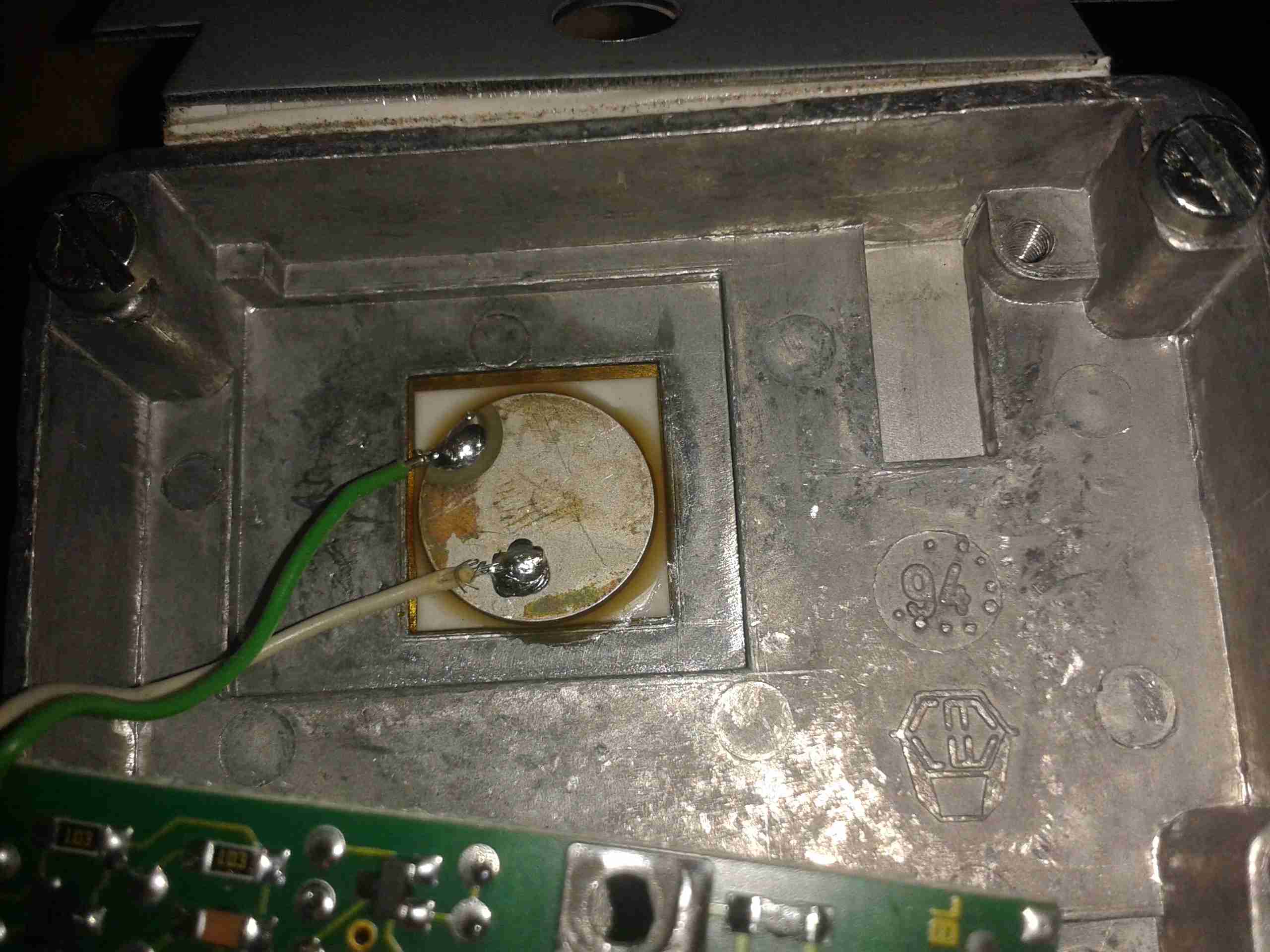
Above is the magnetic mounting plate used to attach the device to the safe. These units are apparently mounted over the keyhole of the safe to protect the lock, so they need to be easily removable to access the safe. This is a very strong magnet & it isn’t possible to pull it from a metal object without triggering the sensor.
Piezo Sensor
Above is the piezo vibration sensor, bonded to the backplate. When the unit receives vibration or shock, this transducer generates a voltage, which is fed to the control logic below.
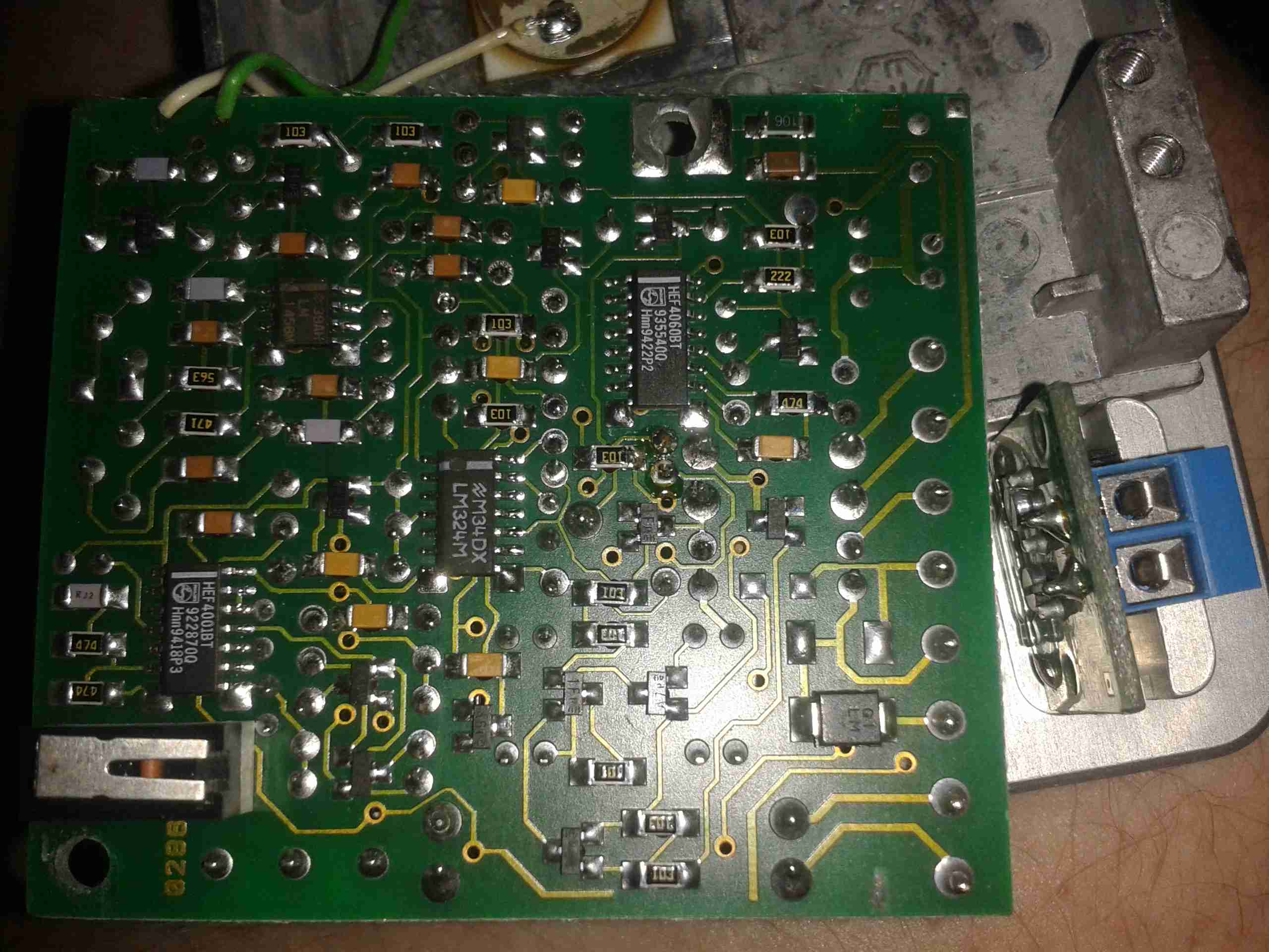
Control Logic
Here’s the reverse of the main PCB with the control logic ICs. These are basic logic gates, with a couple of comparators. One of the tamper switches is in the bottom left corner.
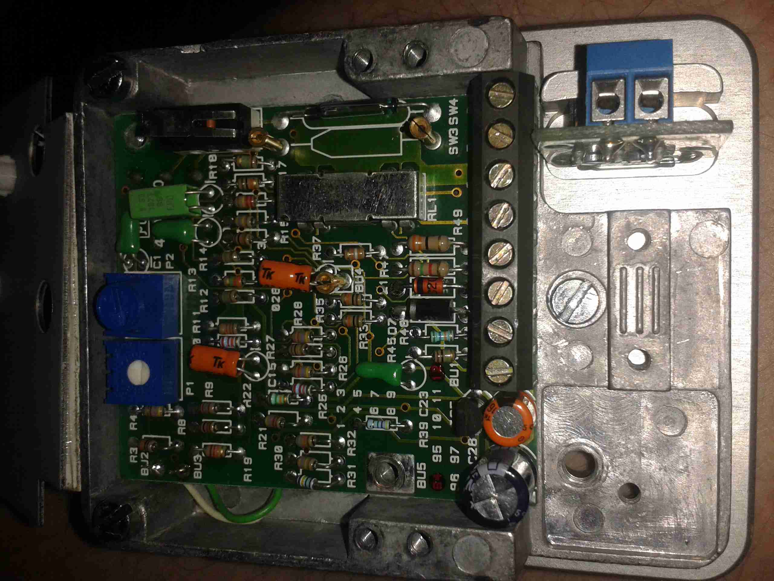
Main PCB
Main PCB with the connection terminals. Another tamper switch is in the top left corner, the solid-state relay is under the shield, next to the magnetic tamper switch. (Reed switch).
Some adjustment is provided for sensitivity. I’ve not found much of a difference in sensitivity though when it’s set to different levels.
Reed Tamper
Magnetic reed switch tamper on the right. Main output solid-state relay on the left under the shield.
This unit was given to me after it apparently went faulty. But on applying power it seems to work fine. Must be those experts again 😉
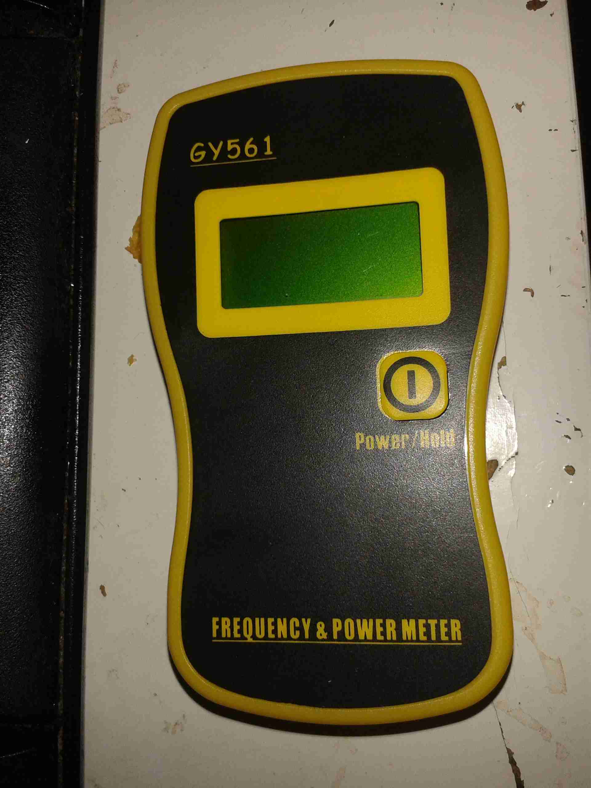
The latest addition to my radio shack is the GY561 frequency & power meter, which has already come in useful for measuring the output power of all my radios.
GY561
It’s a small device, roughly the same size & weight as a stock UV-5R. Power is provided by 3 AAA cells.
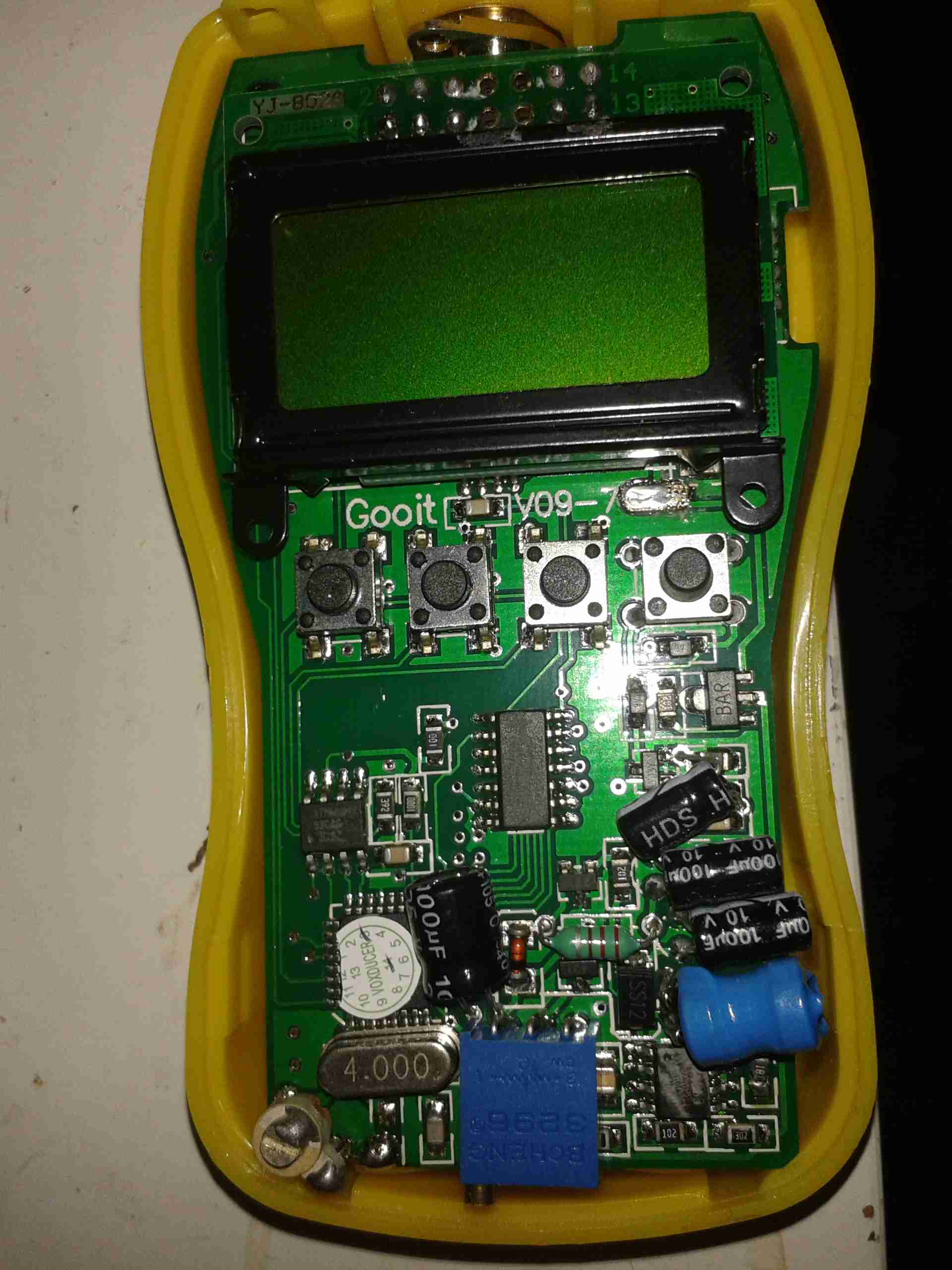
Display
The display is a standard HD44780 8×2 module. The display on this unit isn’t backlit, so no operating in the dark.
Cover Removed
The cover pops off easily to allow access to the internals, without having to remove any screws!
The 4 screws on the back of the unit hold the heatsink plate for the 50W 50Ω dummy load resistor.
Removing the cover reveals a couple of adjustments, for frequency & RF power calibration.
There are also 3 tactile switches that aren’t on the front panel. According to the manual (which in itself is a masterpiece of Chinglish), they are used to software calibrate the unit if an accurate RF power source is available. I will attempt to do a reasonable translation when time allows.
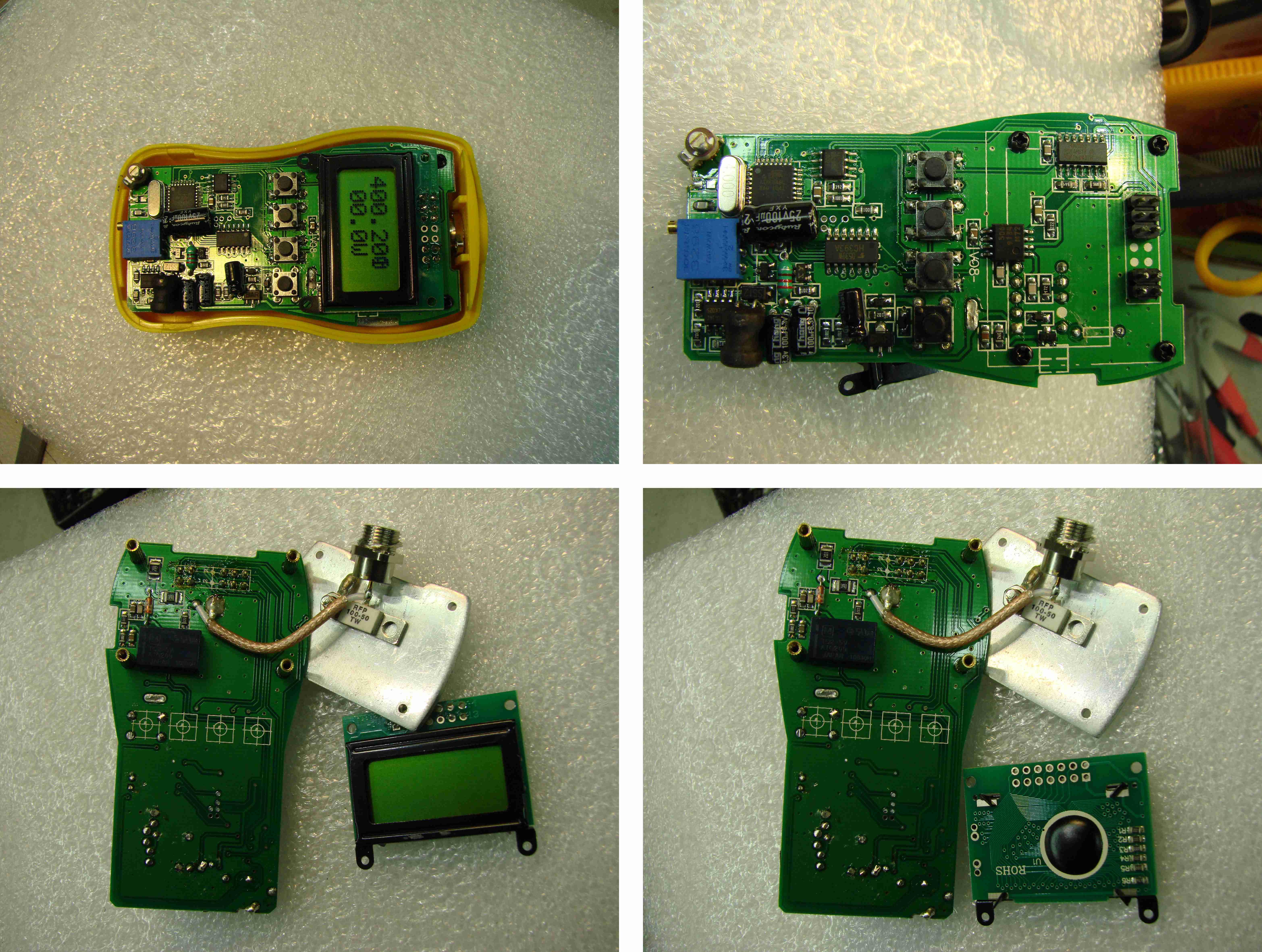
Disassembly further than this involves some desoldering in awkward places, so a search of the internet revealed an image of the rest of the internal components. In the case of my meter, all the part numbers have been scrubbed off the ICs in an attempt to hide their purpose. While it’s possible to cross-reference IC databooks & find the part numbers manually, this process is a time consuming one. Luckily the image I managed to locate doesn’t have the numbers scrubbed.
Total Disassembly
Under the LCD is some 74HC series logic, and a prescaler IC as seen in the previous frequency counter post. However in this unit the prescaler is a MB506 microwave band version to handle the higher frequencies specified.
In this case however the main microcontroller is an ATMEGA8L.
This is complemented by a SN54HC393 4-bit binary counter for the frequency side of things. This seems to make it much more usable down to lower frequencies, although the manual is very generous in this regard, stating that it’s capable of reading down to 1kHz. In practice I’ve found the lowest it reliably reads the frequency input is 10MHz, using my AD9850 DDS VFO Module as a signal source.
It did however read slightly high on all readings with the DDS, but this could have been due to the low power output of the frequency source.
Just like the other frequency counter module, this also uses a trimmer capacitor to adjust the microcontroller’s clock frequency to adjust the calibration.
The power supply circuitry is in the bottom left corner of the board, in this case a small switching supply. The switching regulator is needed to boost the +4.5v of the batteries to +5v for the logic.
Also, as the batteries discharge & their terminal voltage drops, the switching regulator will allow the circuit to carry on functioning. At present I am unsure of the lower battery voltage limit on the meter, but AAA cells are usually considered dead at 0.8v terminal voltage. (2.4v total for the 3 cells).
When turned on this meter draws 52mA from the battery, and assuming 1200mAh capacity for a decent brand-name AAA cell, this should give a battery life of 23 hours continuous use.
On the back of the main PCB is a 5v relay, which seems to be switching an input attenuator for higher power levels, although I only managed to trigger it on the 2m band.
Finally, right at the back attached to an aluminium plate, is the 50Ω dummy load resistor. This component will make up most of the cost of building these, at roughly £15.
On my DVM, this termination reads at about 46Ω, because of the other components on the board are skewing the reading. There are a pair of SMT resistors, at 200Ω & 390Ω in series, and these are connected across the 50Ω RF resistor, giving a total resistance of 46.094Ω.
This isn’t ideal, and the impedance mismatch will probably affect the calibration of the unit somewhat.
The heatsinking provided by the aluminium plate is minimal, and the unit gets noticeably warm within a couple of minutes measuring higher power levels.
High power readings should definitely be limited to very short periods, to prevent overheating.
The RF is sampled from the dummy load with a short piece of Teflon coax.
There’s a rubber duck antenna included, but this is pretty useless unless it’s almost in contact with the transmitting antenna, as there’s no input amplification. It might be handy for detecting RF emissions from power supplies, etc.
For the total cost involved I’m not expecting miracles as far as accuracy is concerned, (the manual states +/-10% on power readings).
The frequency readout does seem to be pretty much spot on though, and the ability to calibrate against a known source is handy if I need some more accuracy in the future.
I’ve also done an SWR test on the dummy load, and the results aren’t good.
At 145.500 MHz, the SWR is 3:1, while at 433.500 it’s closer to 4:1. This is probably due to the lower than 50Ω I measured at the meter’s connector.
These SWR readings also wander around somewhat as the load resistor warms up under power.
I’ll probably also replace the AAA cells with a LiPo cell & associated charge/protection circuitry, to make the unit chargeable via USB. Avoiding disposable batteries is the goal.
Following on from the earlier power tests on my Baofeng HTs, here’s the readings from the Wouxun KG-UV950P. Power is a little lower than specified, but this is probably due to the supply voltage being a bit less than 13.8v. These readings were taken at a supply voltage of 12.88v.
The same frequencies were used, 145.500 & 433.500 for the VHF/UHF tests. For the 6/10m tests 27MHz & 50MHz were used.
The power meter was connected with 1 metre of RG58 dual-screened cable with N-type connectors.
I’ve noticed that the RF power output from the Chinese radios can be quite variable from model to model, and even from individual radios of the same model & batch.
I’ve bought an RF Power meter (GY561) to do some tests on the HTs I have at present.
All tests were performed with the radio fully charged & still on the charging base, to make sure the supply voltage remained constant at 8.4v throughout the tests.
Frequencies used were 145.500 & 433.500 for VHF & UHF respectively.
The power meter was connected with ~8″ of RG174 Coax.
Recently I decommissioned some networking equipment, and discovered the power supplies in some switches were single rail 12v types, with a rather high power rating. I figured these would be very good for powering my Ham radio gear.
They’re high quality Delta Electronics DPSN-150BP units, rated at a maximum power output of 156W.
Label
These supplies have an adjustment pot for the output voltage regulation, but unfortunately it just didn’t have quite enough range to get from 12.0v to 13.8v. The highest they would go was ~13.04v.
After taking a look at the regulator circuit, I discovered I could further adjust the output voltage by changing a single resistor to a slightly lower value.
Firstly though, a little background on how switched mode power supplies operate & regulate their output voltage.
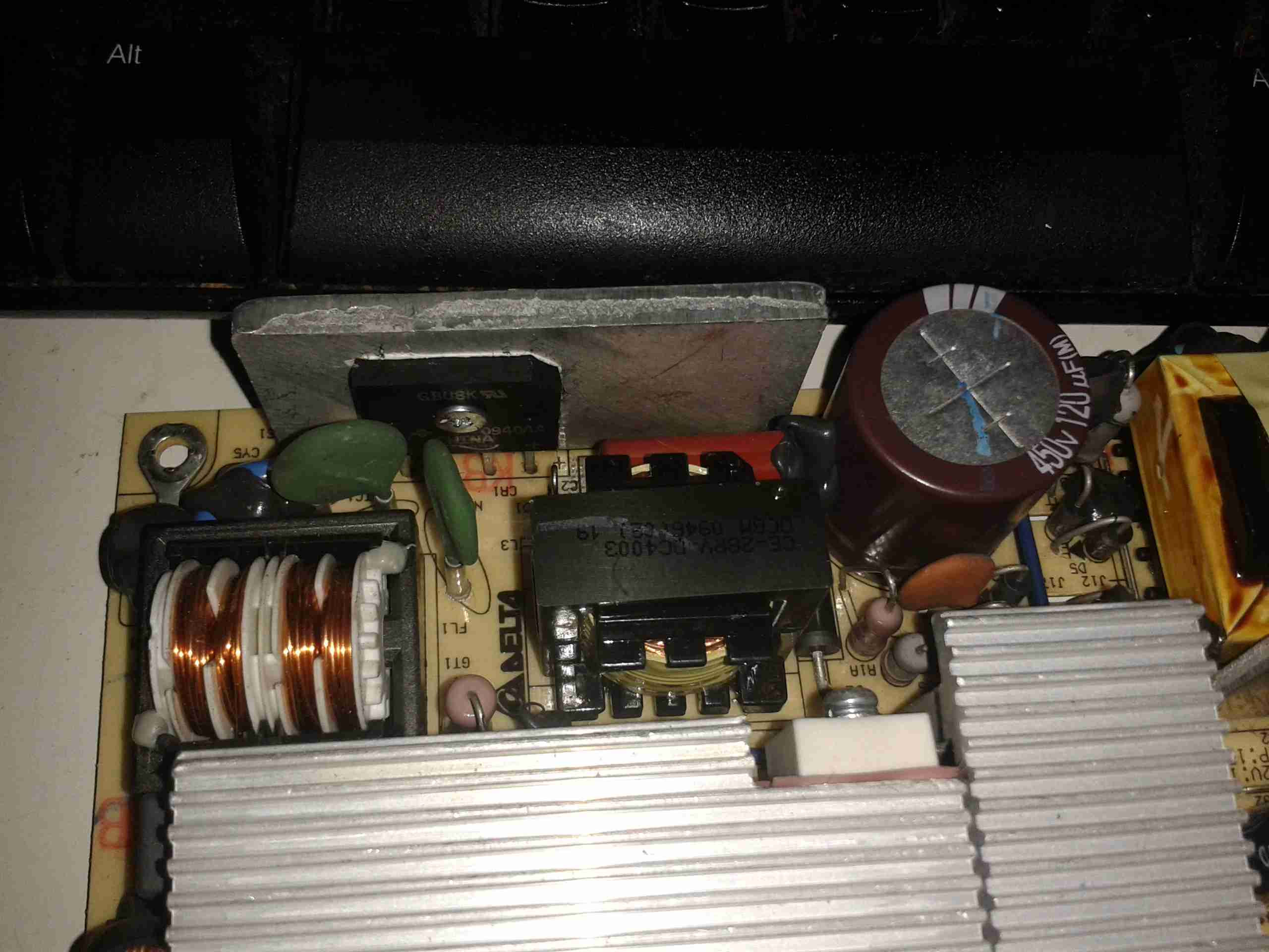
SMPS
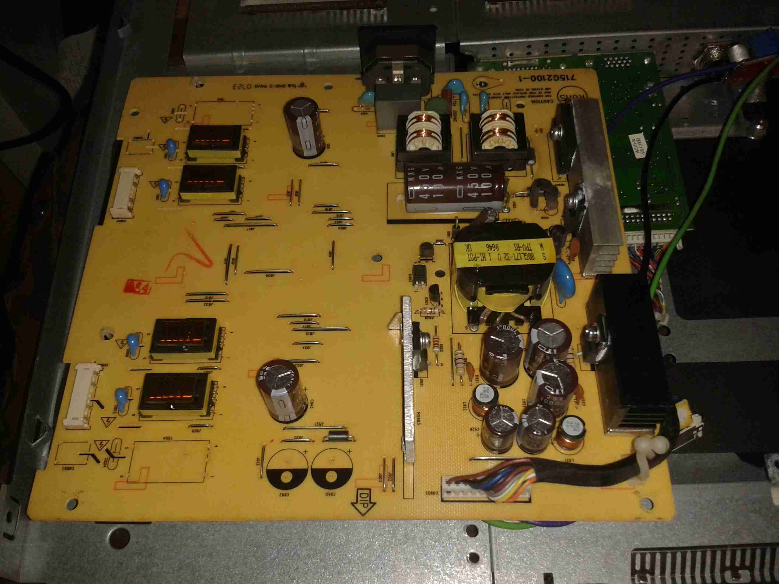
Here’s the supply. It’s mostly heatsink, to cool the large power switching transistors.
The first thing a SMPS does, is to rectify the incoming mains AC with a bridge rectifier. This is then smoothed by a large electrolytic capacitor, to provide a main DC rail of +340v DC (when on a 240v AC supply).
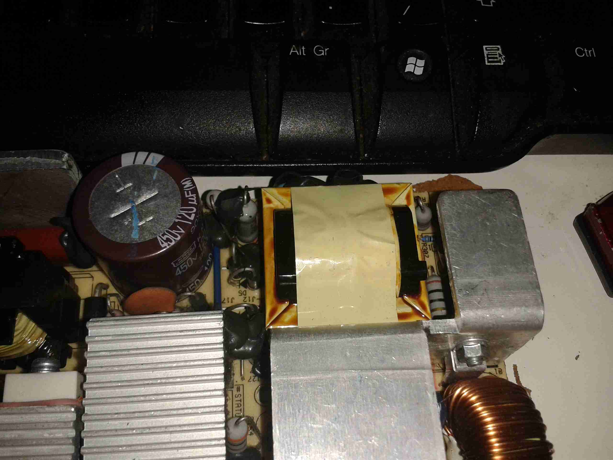
Mains Input
Above is the mains input section of the PSU, with a large common-mode choke on the left, bridge rectifier in the centre, and the large filter capacitor on the right. These can store a lot of energy when disconnected from the mains, and while they should have a discharge resistor fitted to safely drain the stored energy, they aren’t to be relied on for safety!
Once the supply has it’s main high voltage DC rail, this is switched into the main transformer by a pair of very large transistors – these are hidden from view on the large silver heatsinks at the bottom of the image. These transistors are themselves driven with a control IC, in the case of this supply, it’s a UC3844B. This IC is hidden under the large heatsink, but is just visible in the below photo. (IC5).
Control ICMain Switching Transformer
Here’s the main switching transformer, these can be much smaller than a conventional transformer due to the high frequencies used. This supply operates at 500kHz.
After the main transformer, the output is rectified by a pair of Schottky diodes, which are attached to the smaller heatsink visible below the transformer, before being fed through a large toroidal inductor & the output filter capacitors.
All this filtering on both the input & the output is required to stop these supplies from radiating their operating frequency as RF – a lot of cheap Chinese switching supplies forego this filtering & as a result are extremely noisy.
After all this filtering the DC appears at the output as usable power.
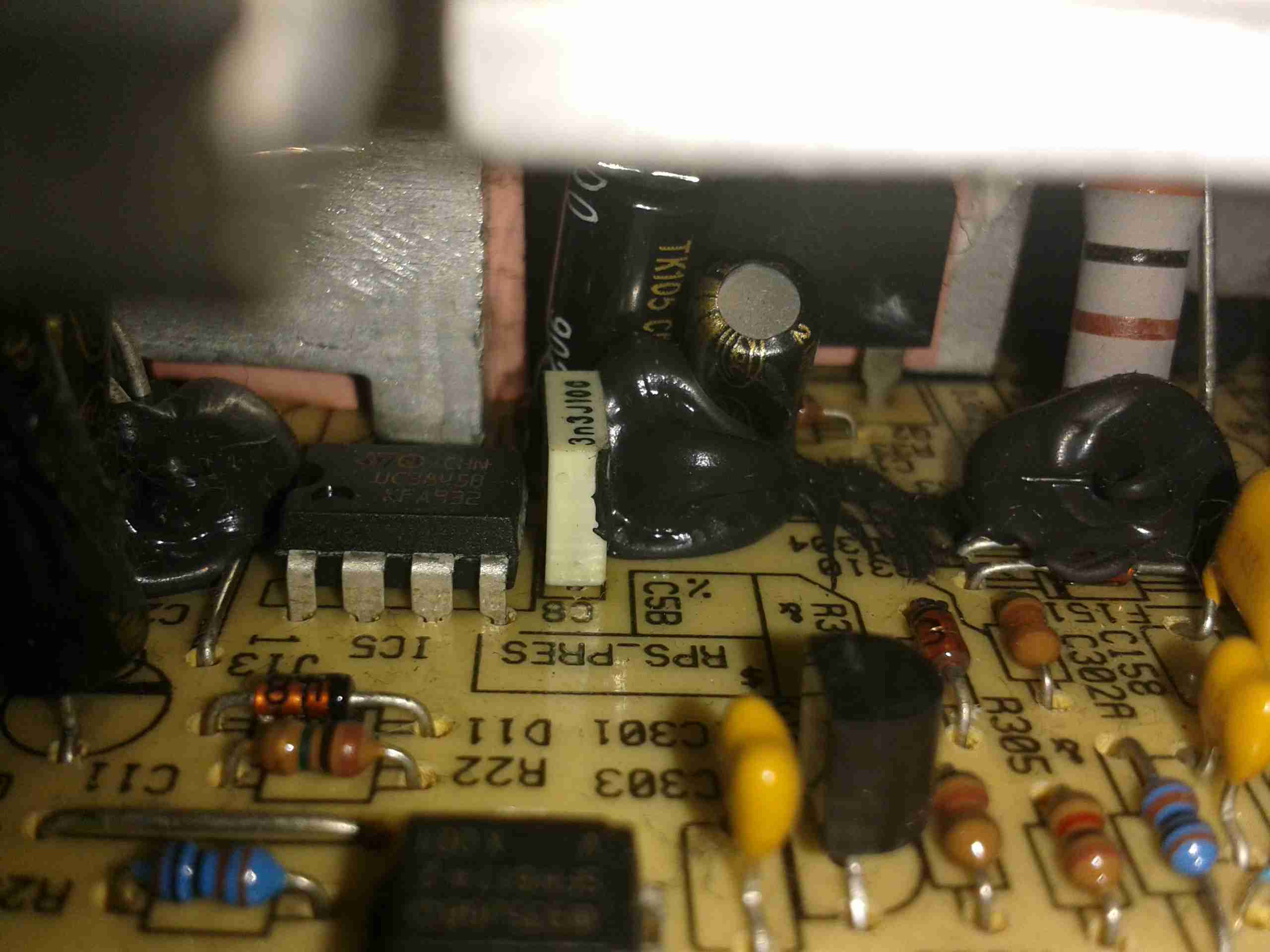
Getting back to regulation, these supplies read the voltage with a resistor divider & feed it back to the mains side control IC, through an opto-isolator. (Below).
Feedback Loop
The opto isolators are the black devices at the front with 4 pins.
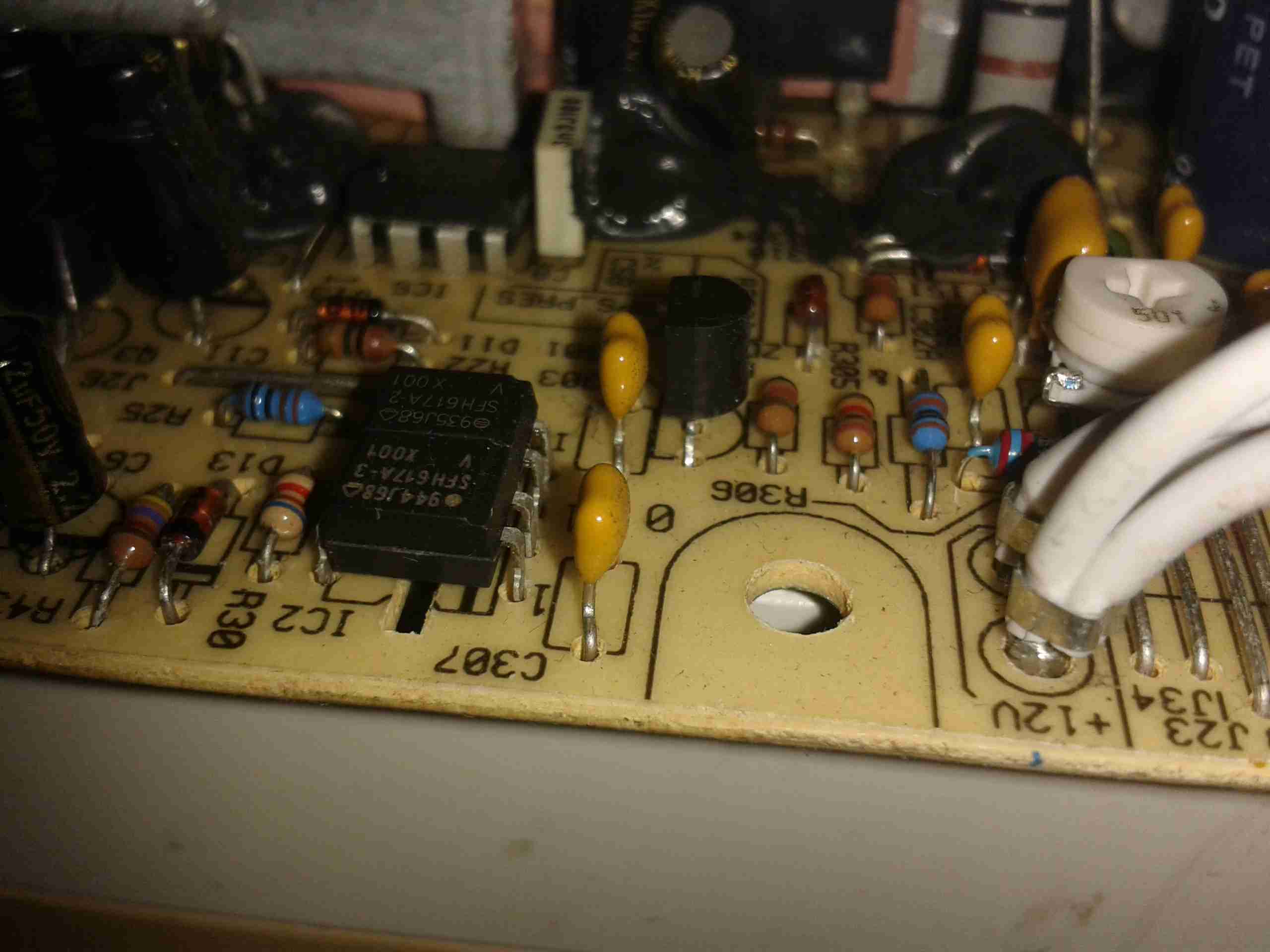
Regulator Adjustment
For a more in-depth look at the inner workings of SMPS units, there’s a good article over on Hardware Secrets.
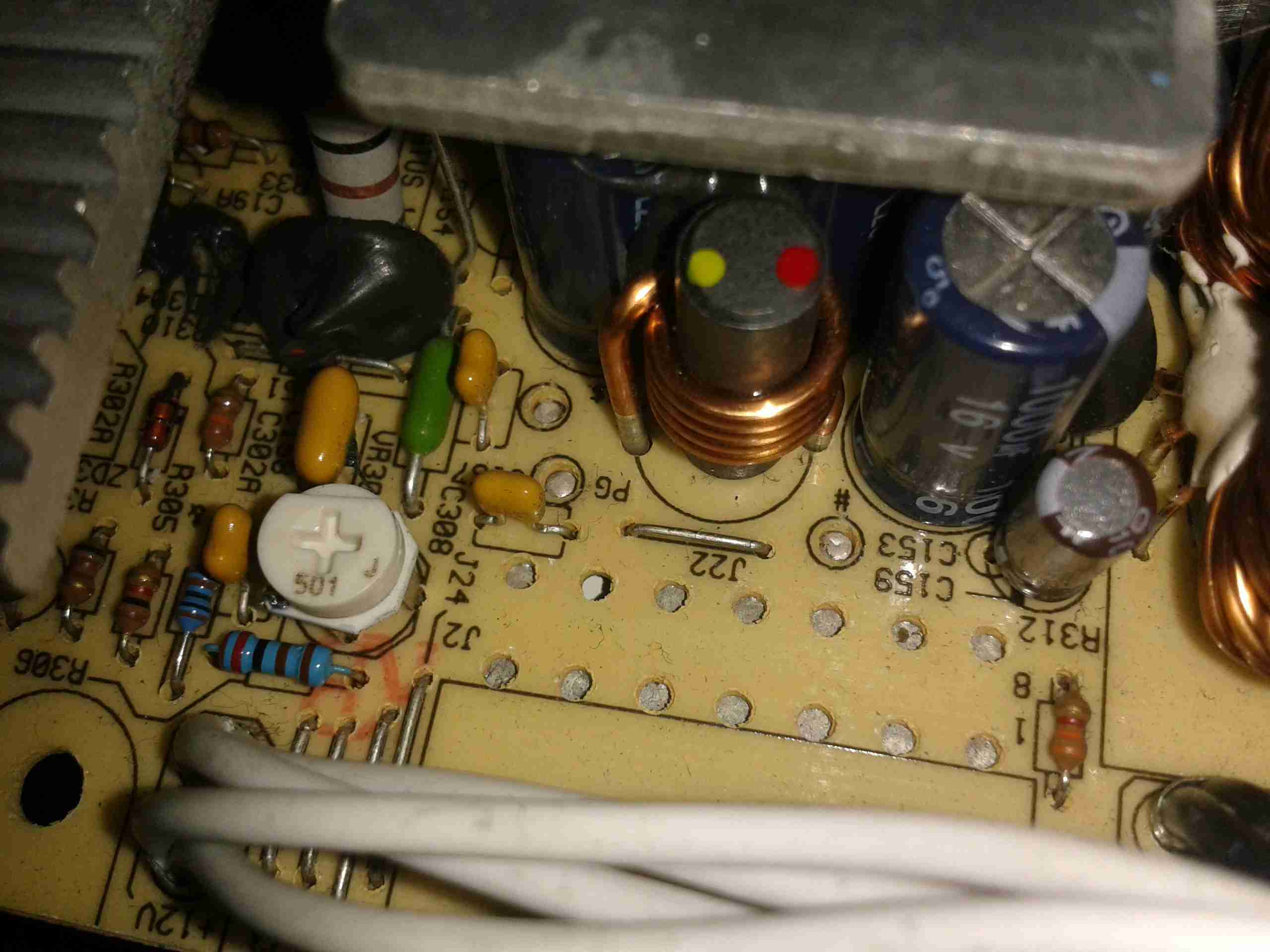
My modification is simple. Replacing R306 (just below the white potentiometer in the photo), with a slightly smaller resistor value, of 2.2KΩ down from 2.37KΩ, allows the voltage to be pulled lower on the regulator. This fools the unit into applying more drive to the main transformer, and the output voltage rises.
It’s important to note that making too drastic a change to these supplies is likely to result in the output filter capacitors turning into grenades due to overvoltage. The very small change in value only allows the voltage to rise to 13.95v max on the adjuster. This is well within the rating of 16v on the output caps.
Now the voltage has been sucessfully modified, a new case is on the way to shield fingers from the mains. With the addition of a couple of panel meters & output terminals, these supplies will make great additions to my shack.
I recently posted about a small analog SWR/Power meter I got from eBay, and figured it needed some improvement.
After some web searching I located a project by ON7EQ, an Arduino sketch to read SWR & RF power from any SWR bridge.
The Arduino code is on the original author’s page above, his copyright restrictions forbid me to reproduce it here.
I have also noticed a small glitch in the code when it is flashed to a blank arduino: The display will show scrambled characters as if it has crashed. However pushing the buttons a few times & rebooting the Arduino seems to fix this. I think it’s related to the EEPROM being blank on a new Arduino board.
I have run a board up in Eagle for testing, shown below is the layout:
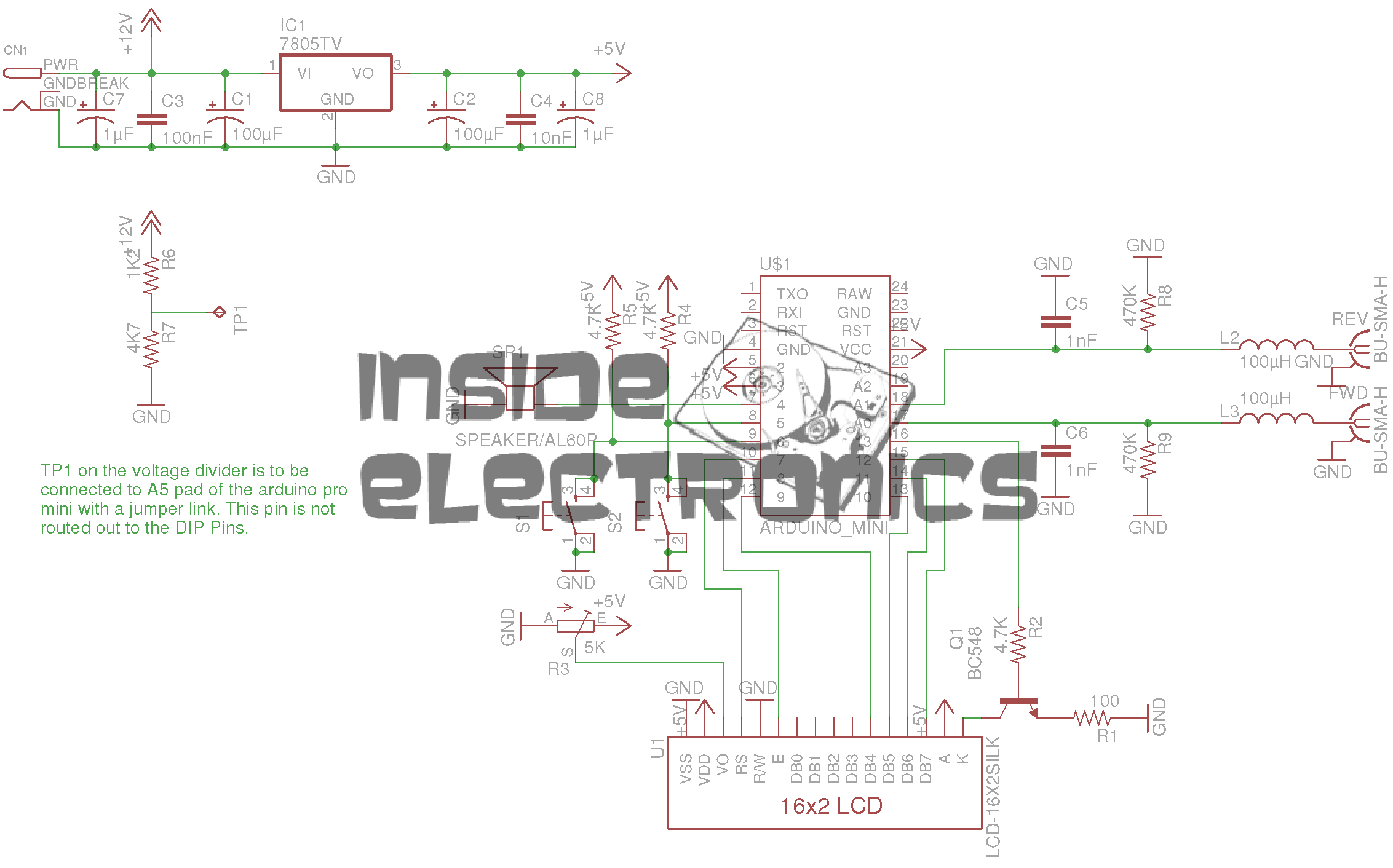
SWR Meter SCH
The Schematic is the same as is given on ON7EQ’s site. Update: ON7EQ has kindly let me know I’ve mixed up R6 & R7, so make sure they’re switched round when the board is built ;). Fitting the resistors the wrong way around may damage the µC with overvoltage.
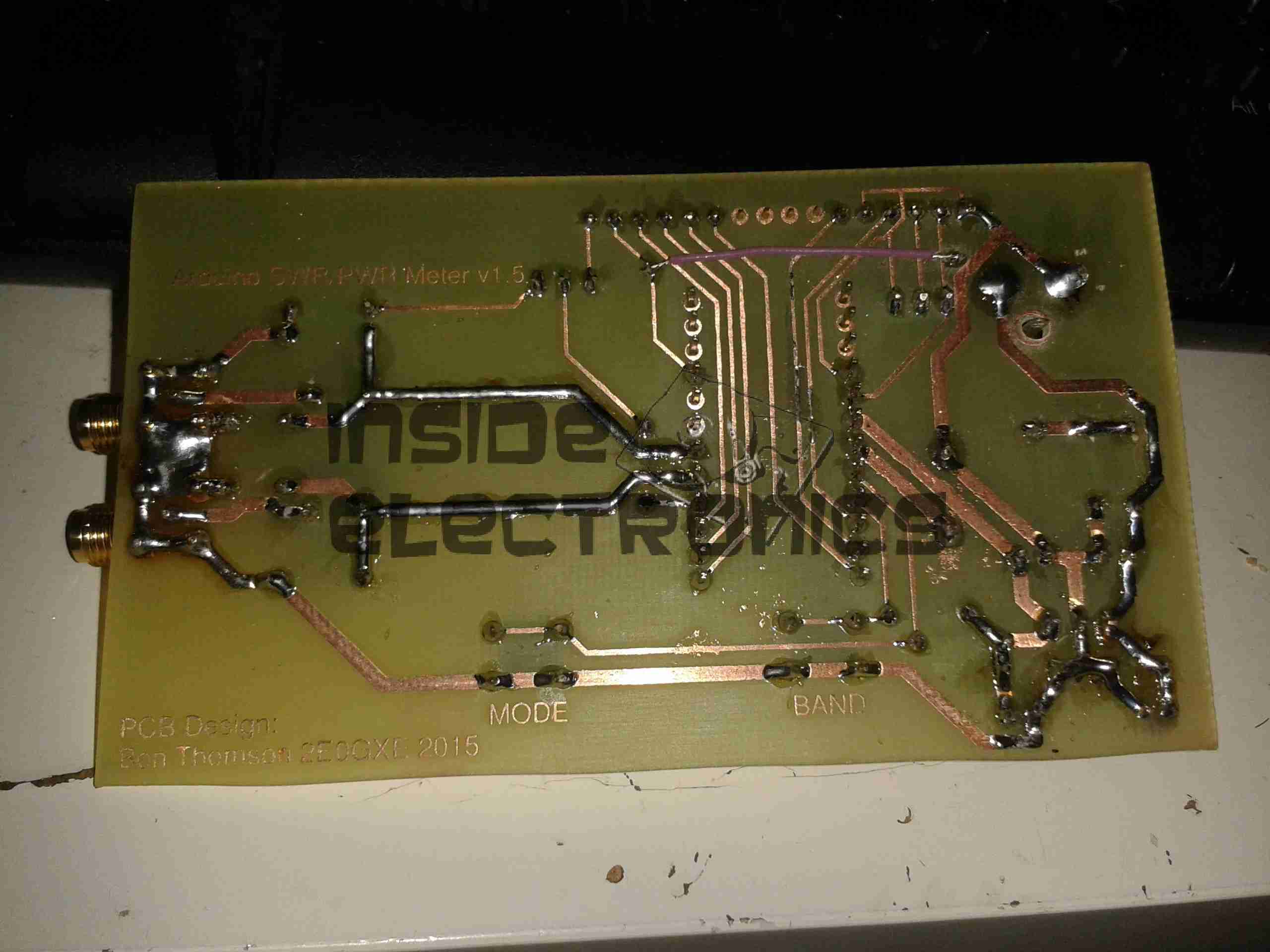
SWR Meter PCB
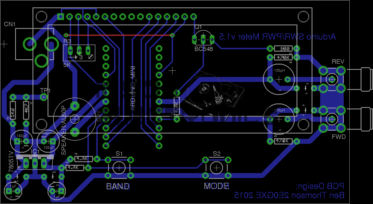
Here’s the PCB layout. I’ve kept it as simple as possible with only a single link on the top side of the board.
PCB Top
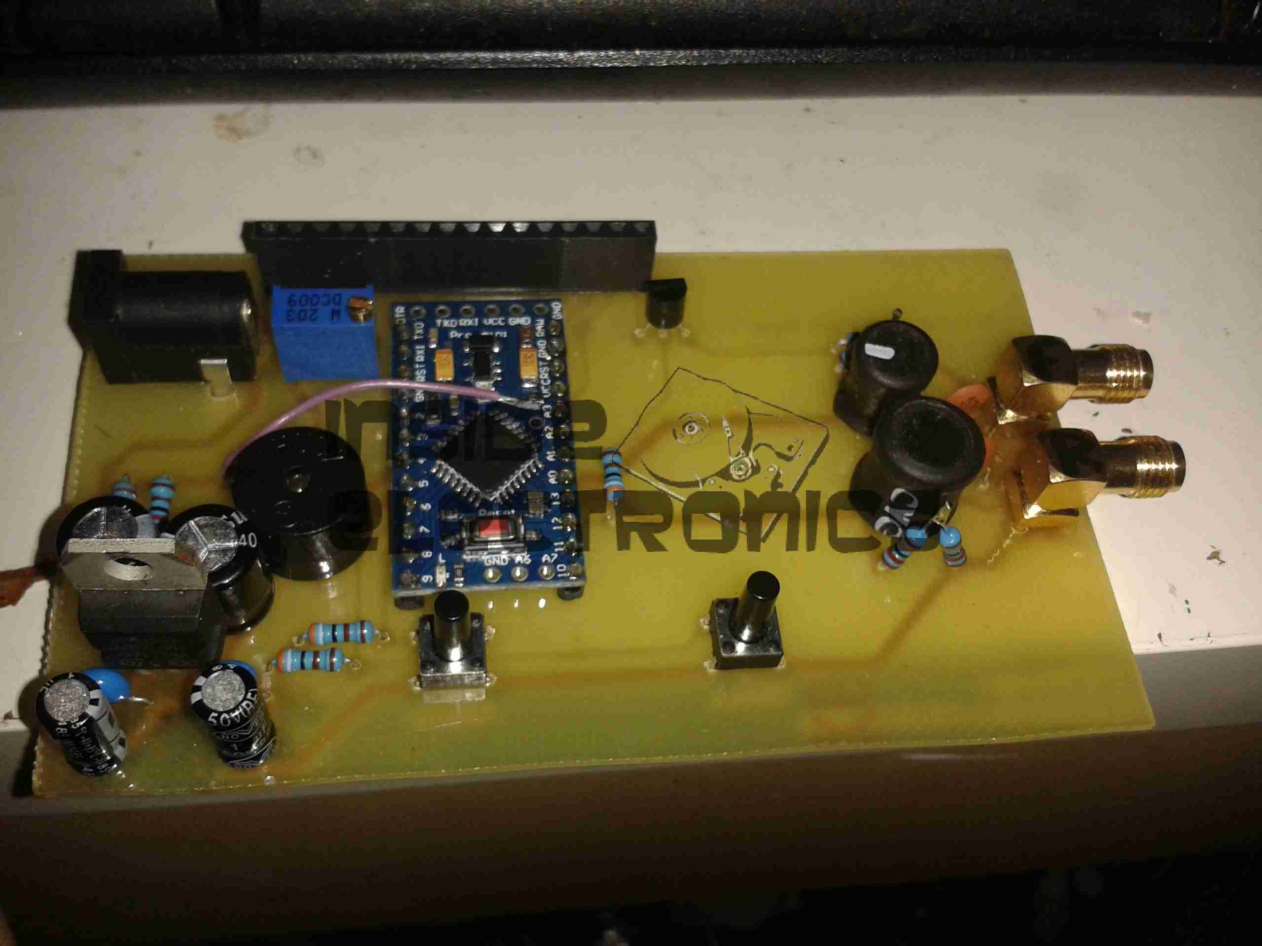
Here’s the freshly completed PCB ready to rock. Arduino Pro mini sits in the center doing all the work.
The link over to A5 on the arduino can be seen here, this allows the code to detect the supply voltage, useful for battery operation.
On the right hand edge of the PCB are the pair of SMA connectors to interface with the SWR bridge. Some RF filtering is provided on the inputs.
PCB Bottom
Trackside view of the PCB. This was etched using my tweaked toner transfer method.
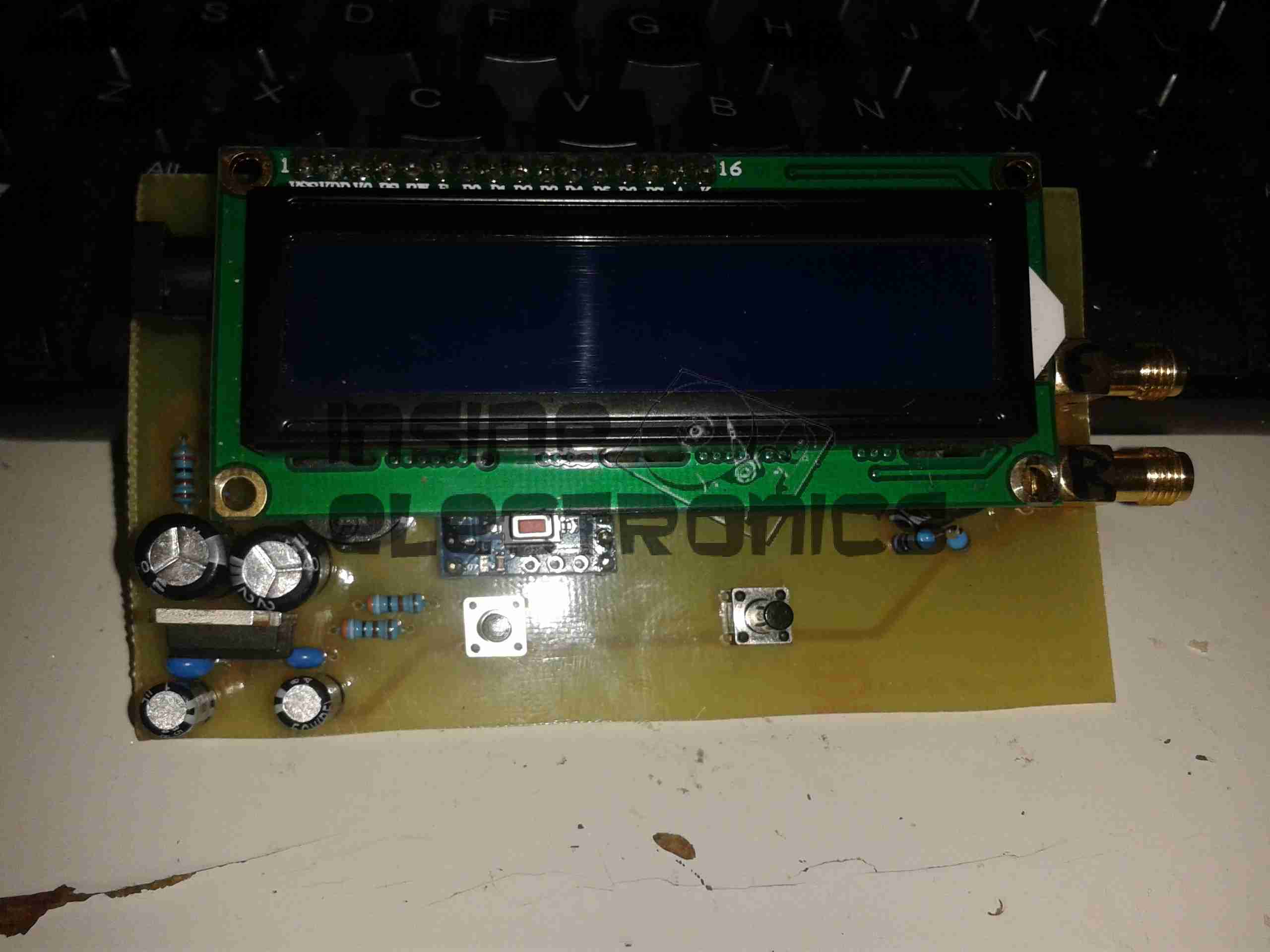
LCD Fitted
Here the board has it’s 16×2 LCD module.
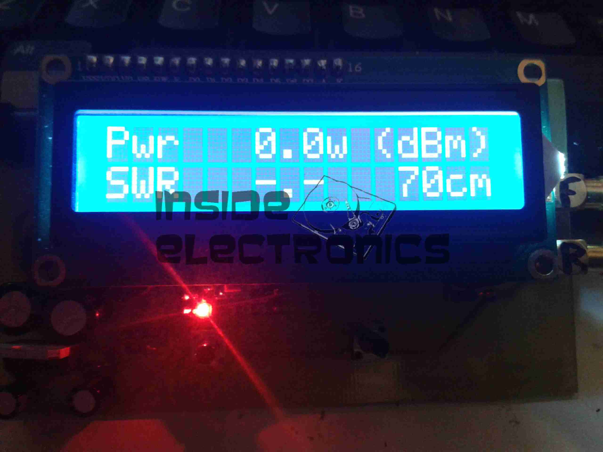
Online
Board powered & working. Here it’s set to the 70cm band. The pair of buttons on the bottom edge of the board change bands & operating modes.
As usual, the Eagle layout files are available below, along with the libraries I use.
[download id=”5585″]
[download id=”5573″]
More to come on this when some components arrive to interface this board with the SWR bridge in the eBay meter.
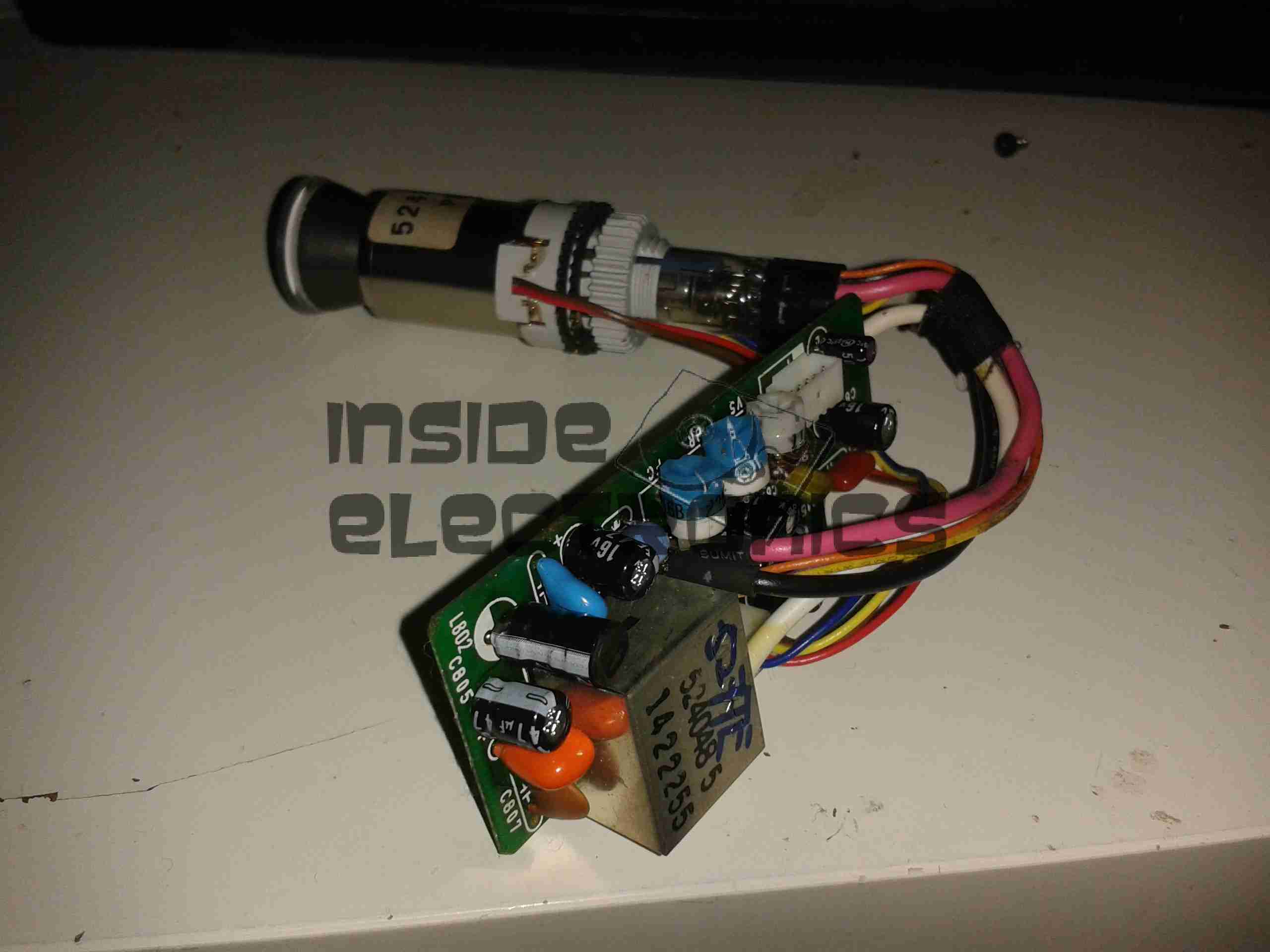
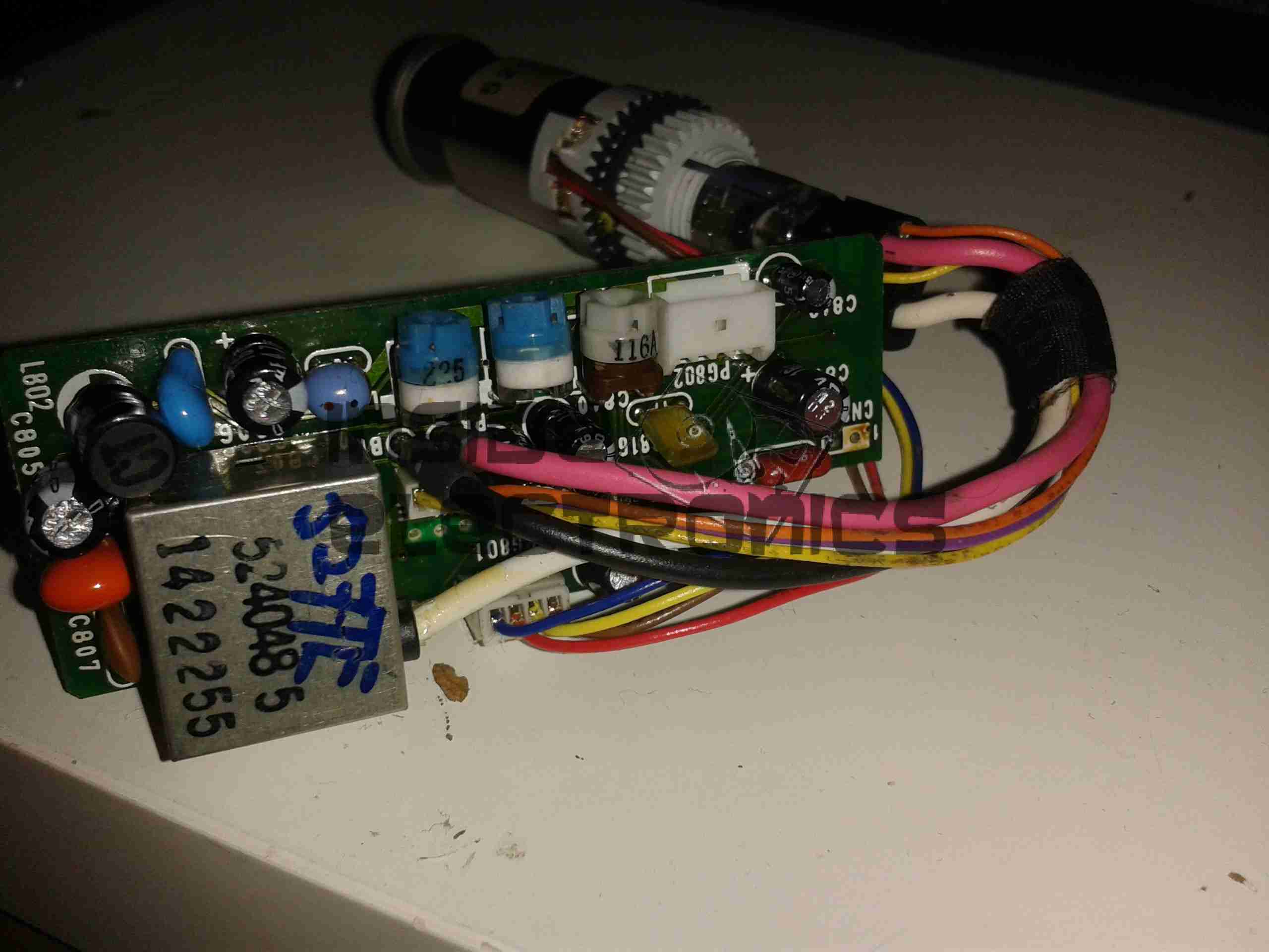
Here’s another viewfinder CRT, removed from a 1980’s vintage VHS camera I managed to get cheap from eBay.
This unit is very similar to the last one I posted about, although there are a few small differences in the control circuitry.
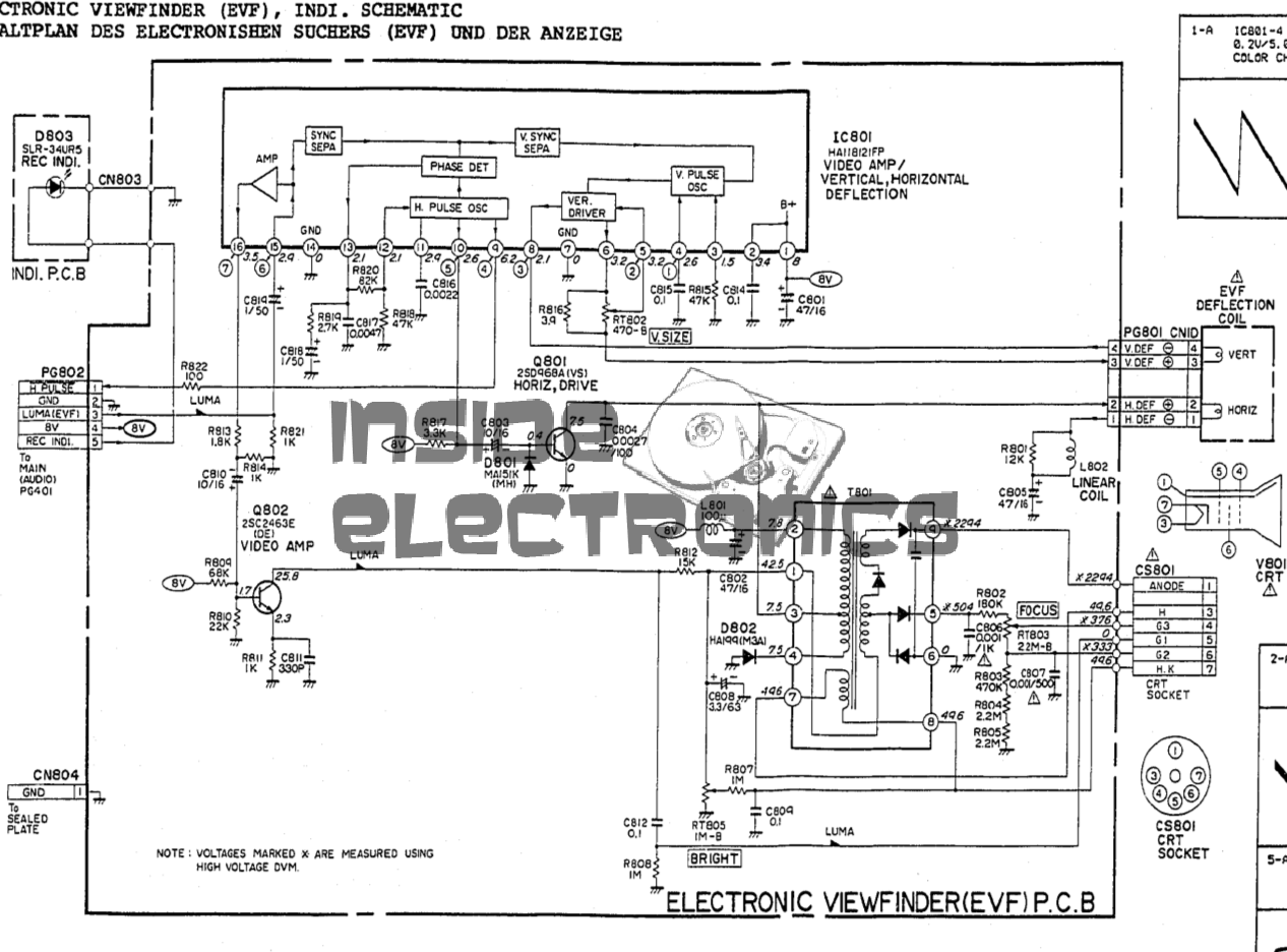
Viewfinder Schematic – Click to Embiggen
Here’s the schematic, showing all the functional blocks of the viewfinder circuitry. An integrated viewfinder IC is used, which generates all the required scan waveforms for the CRT.
On the left is the input connector, with the power & video signals. Only pins 2 (GND), 3 (Composite video), & 4 (+8v) are needed here. Pin 1 outputs a horizontal sync signal for use elsewhere in the camera, while pin 5 fed the recording indicator LED.
To make connection easier, I have rearranged the wires in the input connector to a more understandable colour scheme:
Input Connector
Red & Blue for power input, & a coax for the video. For the video GND connection, I have repurposed the Rec. LED input pin, putting a shorting link across where the LED would go to create a link to signal ground. Keeping this separate from the power GND connection reduces noise on the CRT.
Viewfinder CRT Assembly
Here’s the complete assembly liberated from it’s plastic enclosure.
PCB Closeup
Closeup of the control PCB. The 3 potentiometers control the CRT brightness, focus & vertical size.
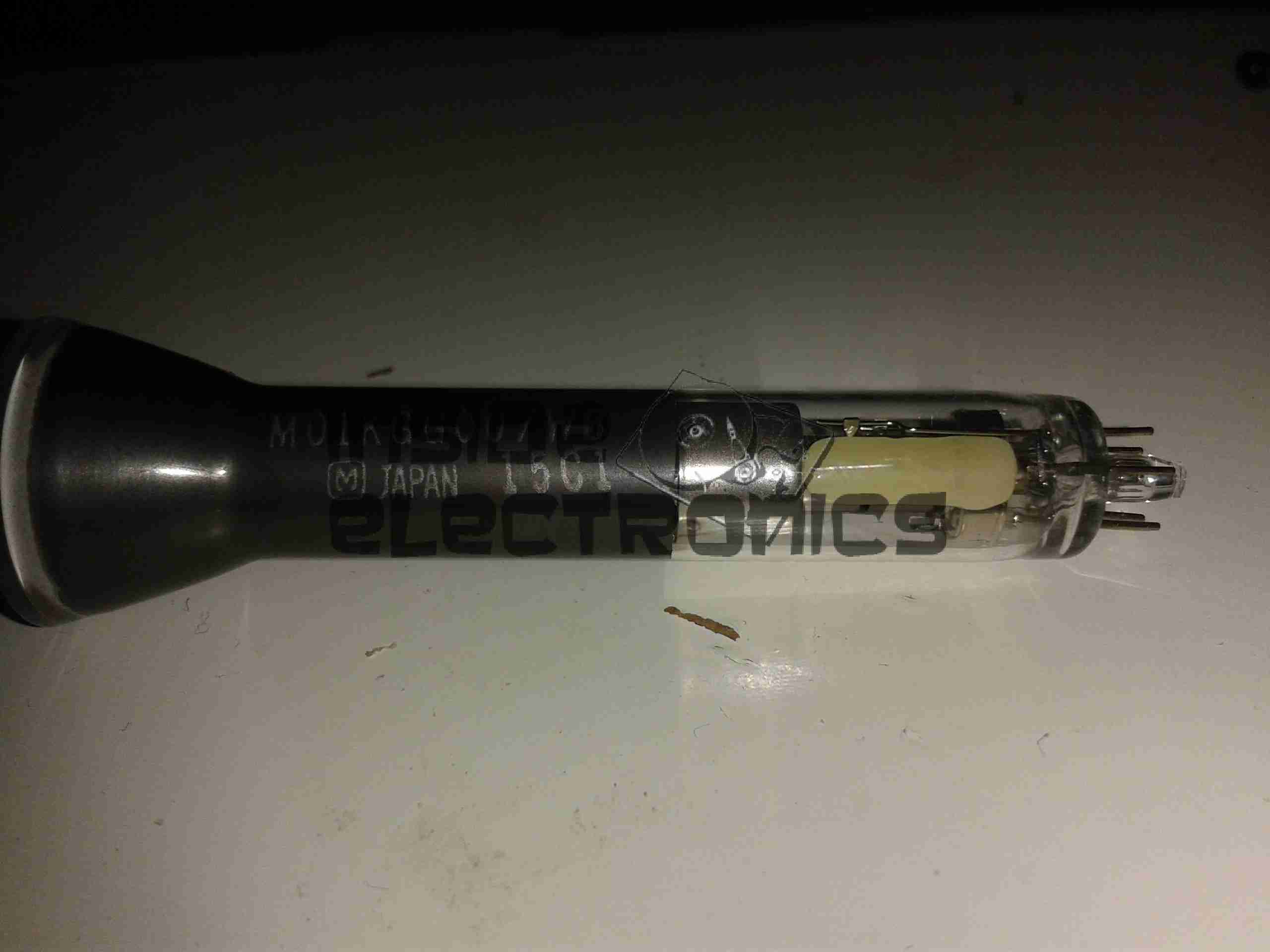
M01KGG007WB CRT
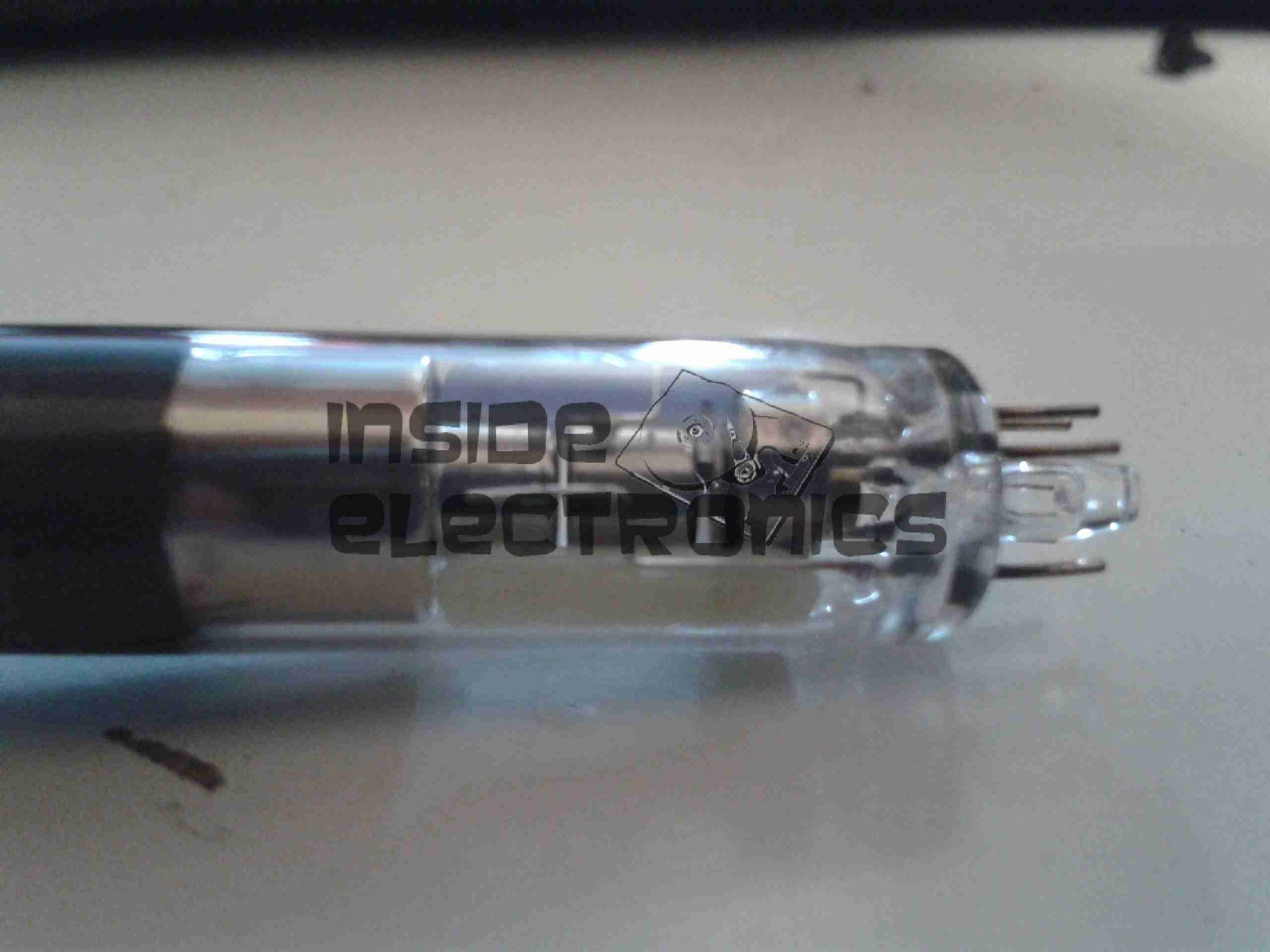
The tiny CRT. Only ~60mm in length, with an 18mm screen size. This tube runs on +2294v final anode voltage. Much higher than I expected.
Electron Gun Closeup
The electron gun assembly, with the cathode, focus & final anode cups.
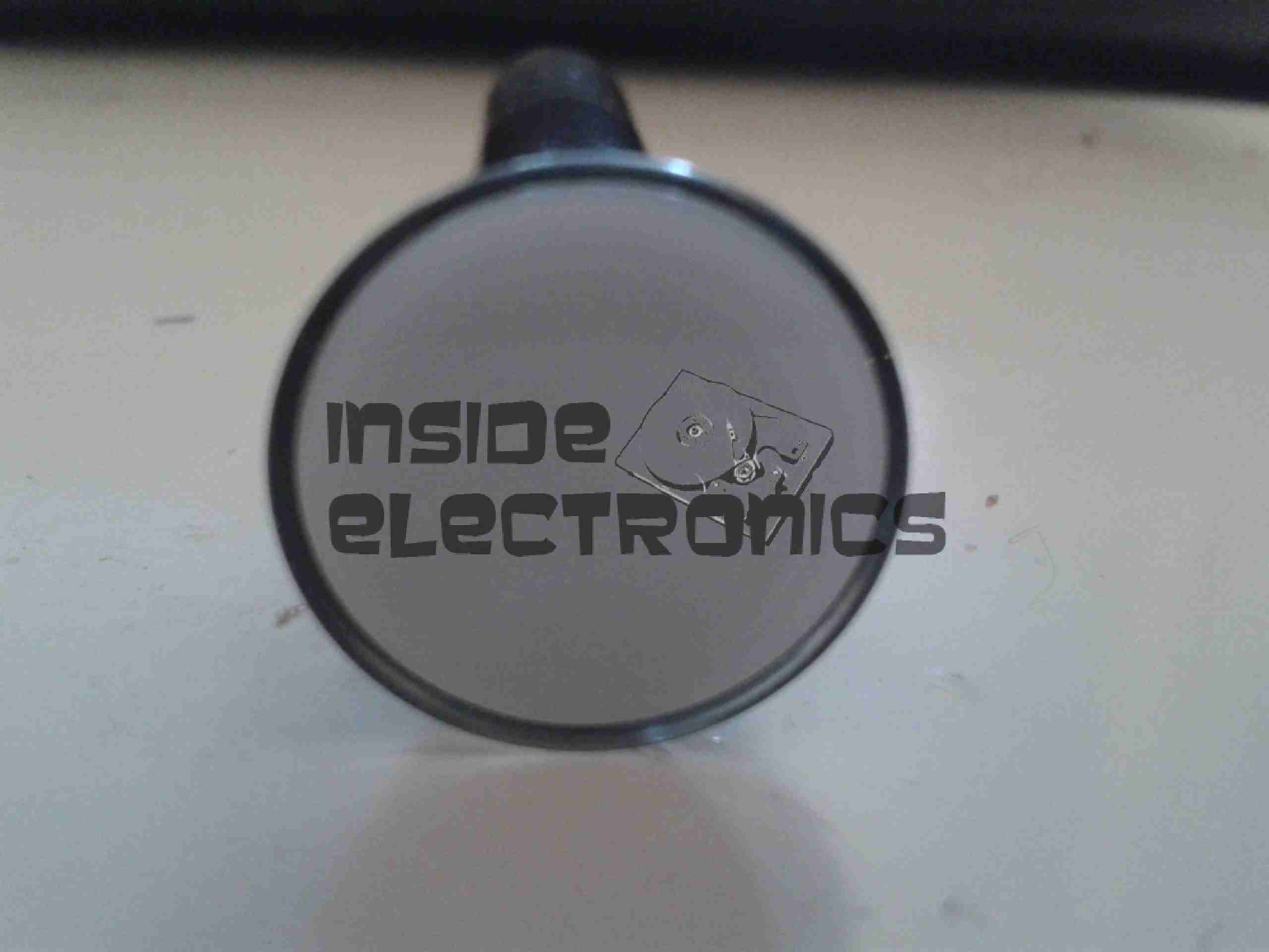
Phosphor Screen
This screen is just a little bigger than a UK 5p piece! A marvel of precision engineering.
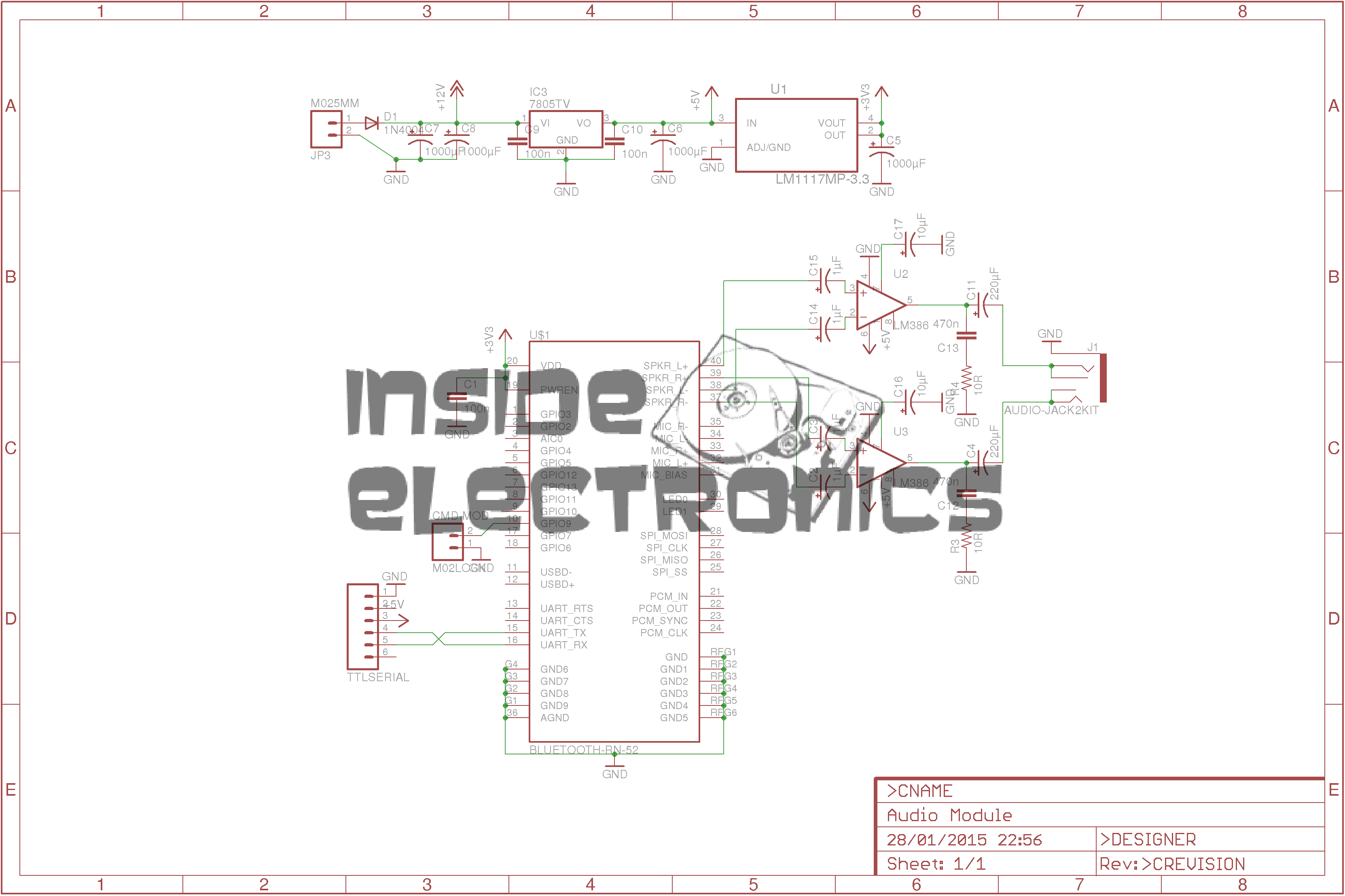
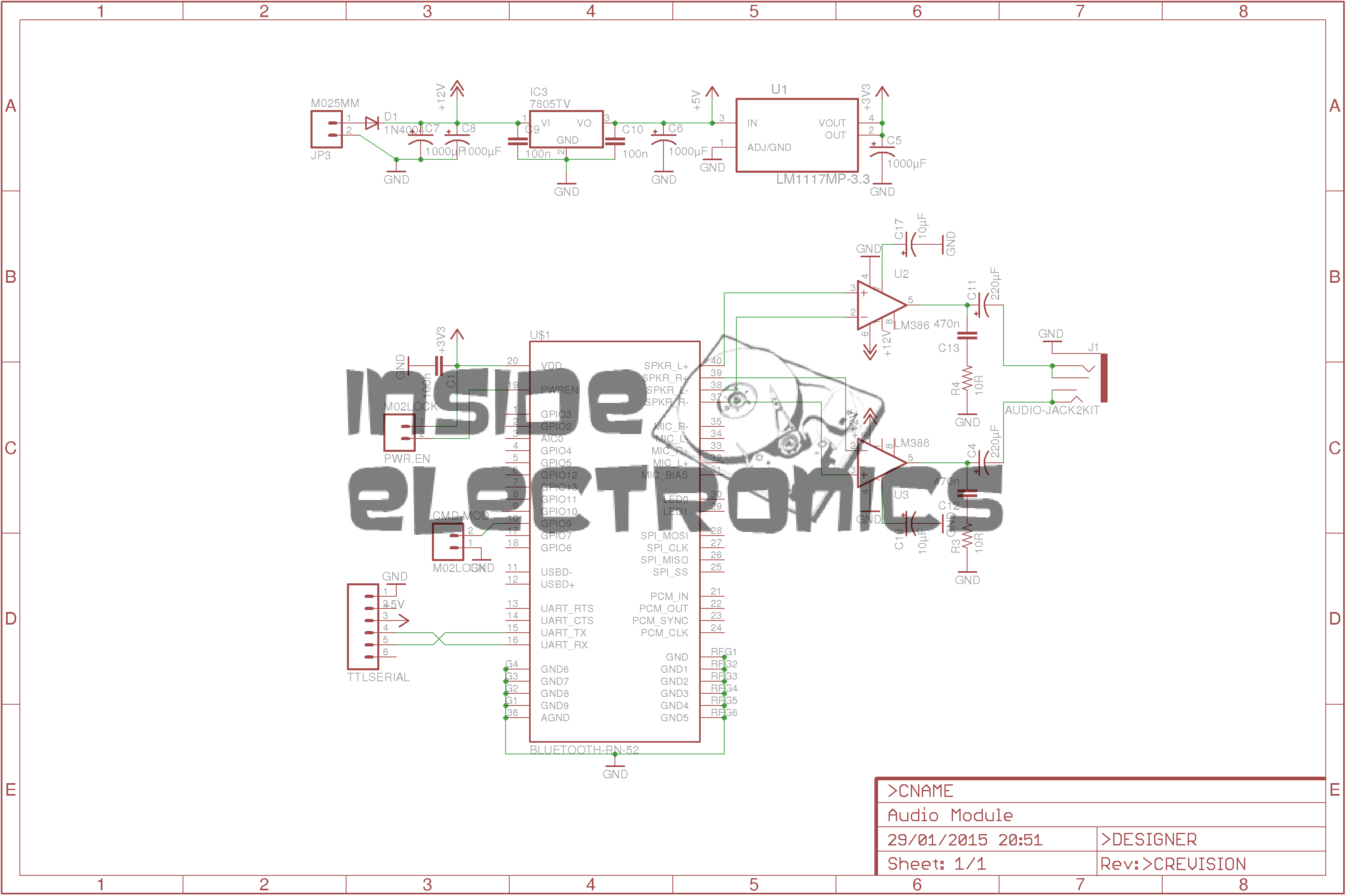
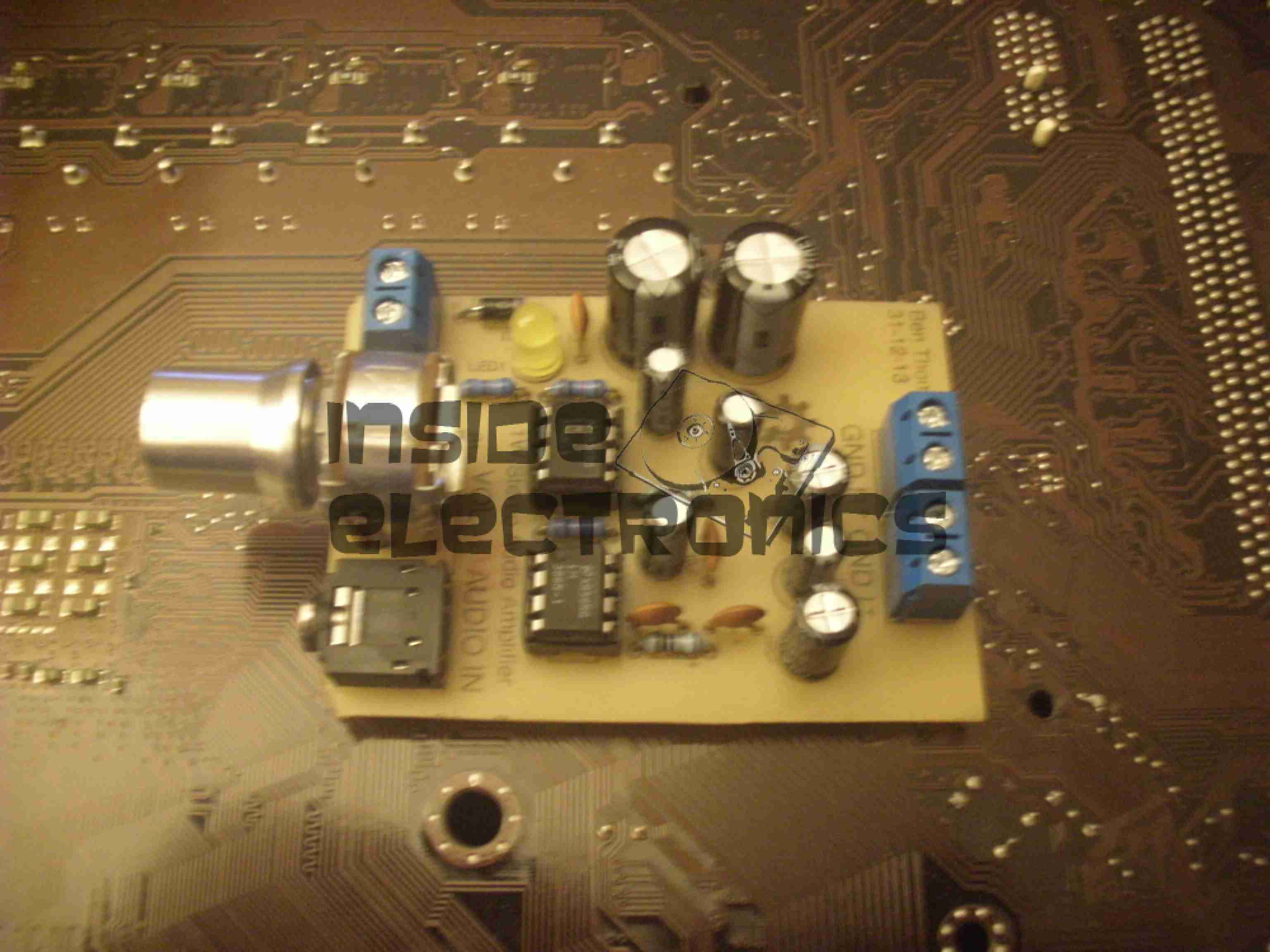
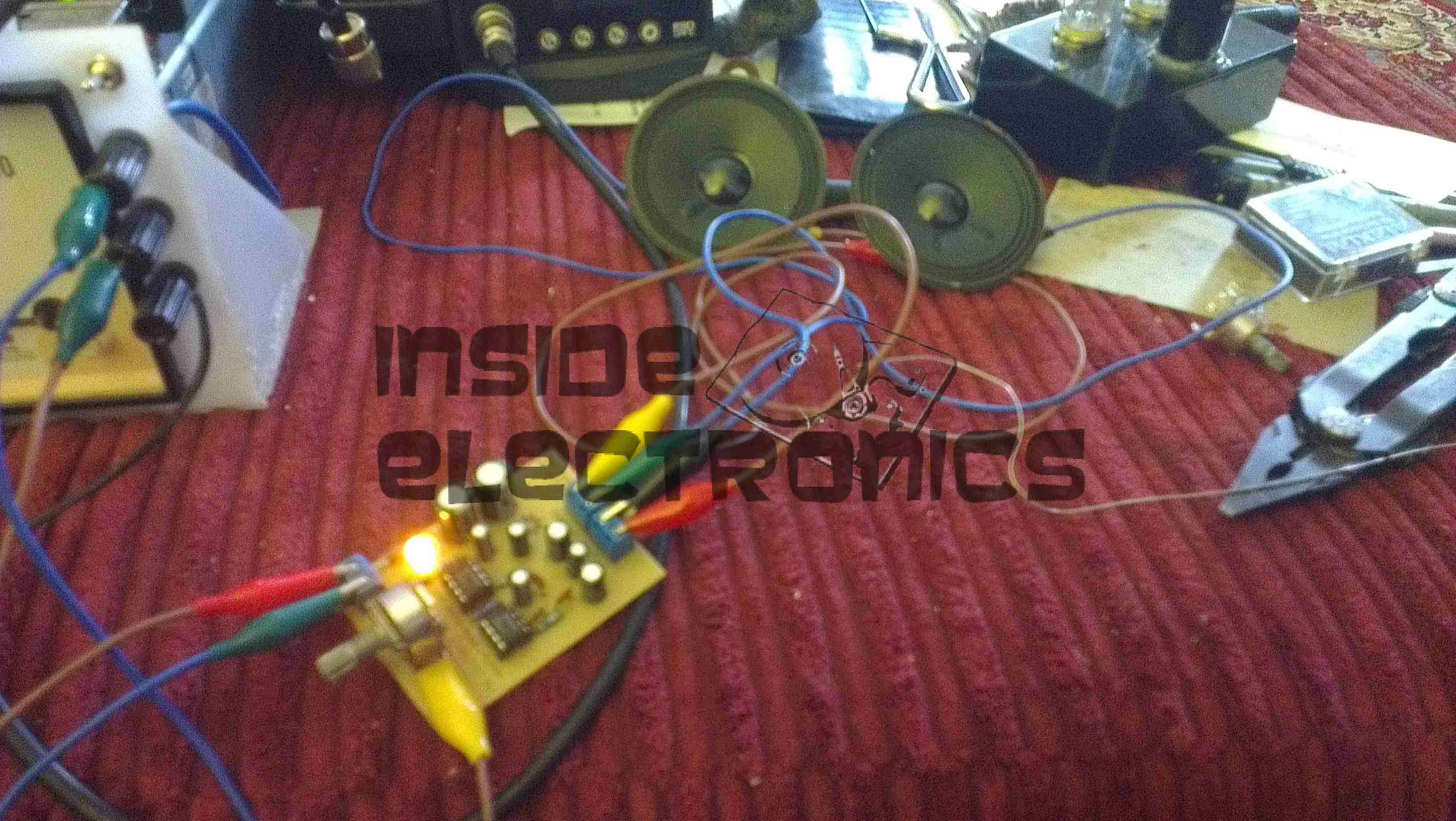
I’ve been doing some tinkering with the RN-52 Bluetooth Audio module from Roving Networks, in prep for building a portable wireless speaker system, & thought I’d share my designs.
Initially I was having some issues with RF noise on the audio output from the RN-52, as I was only using the outputs single-ended. The module didn’t like this treatment, with all the RF whine coming straight out of the speakers.
To fix this issue I have used a pair of jellybean LM386 audio power amplifiers, running in differential input mode. This solves the high-pitched whine when the audio is enabled, & also allows the module to directly drive a set of 32Ω headphones at a reasonable level.
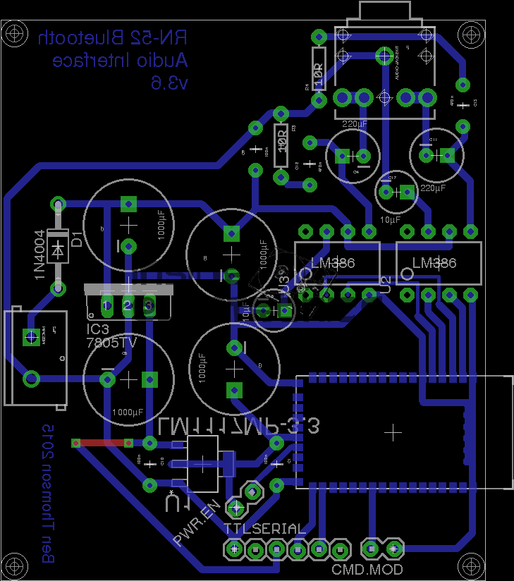
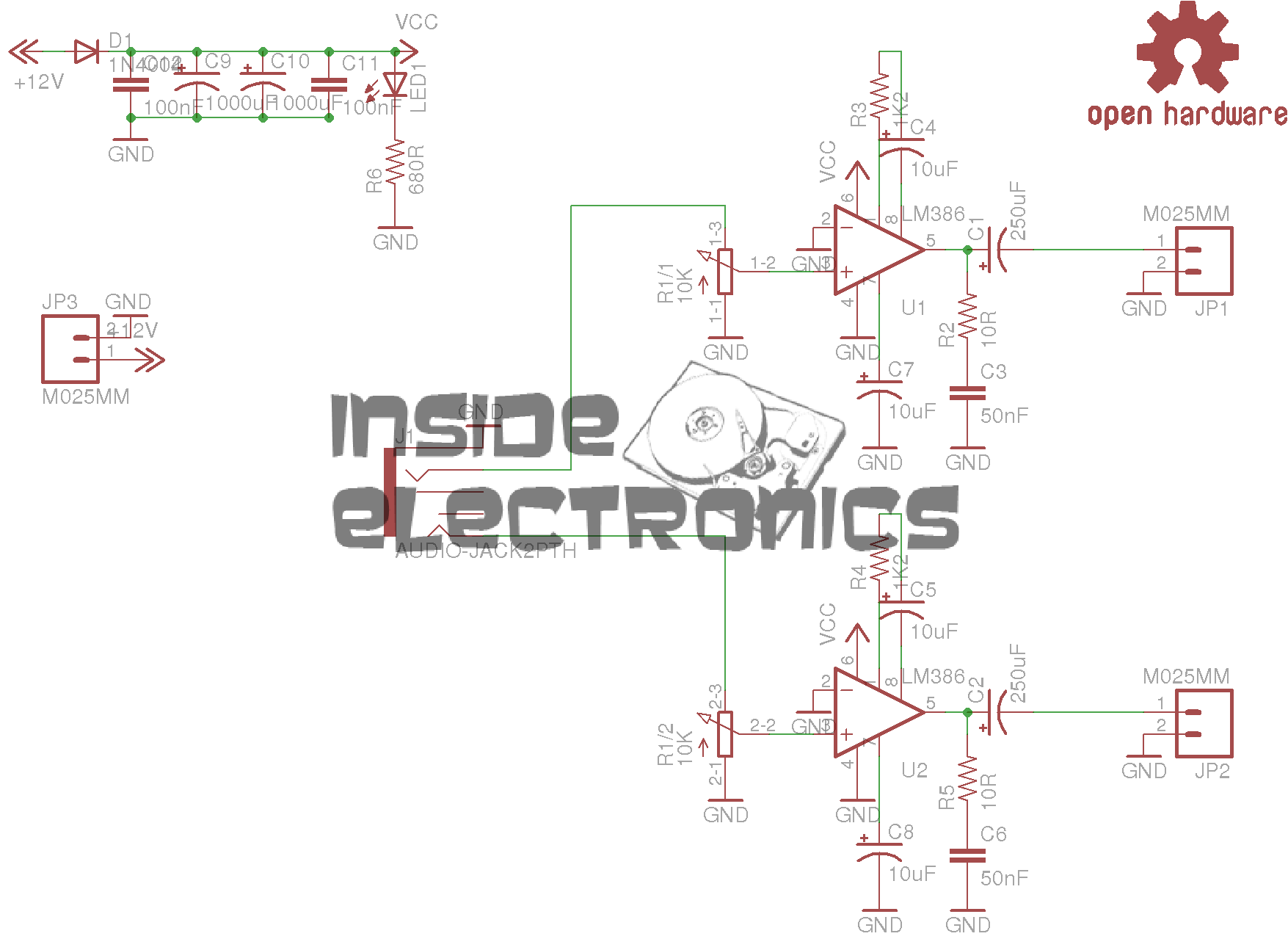
In Eagle I have designed a simple board, routing only the audio output, serial TTL & command mode pins out, along with the supporting power supply circuitry to operate from 12v DC.
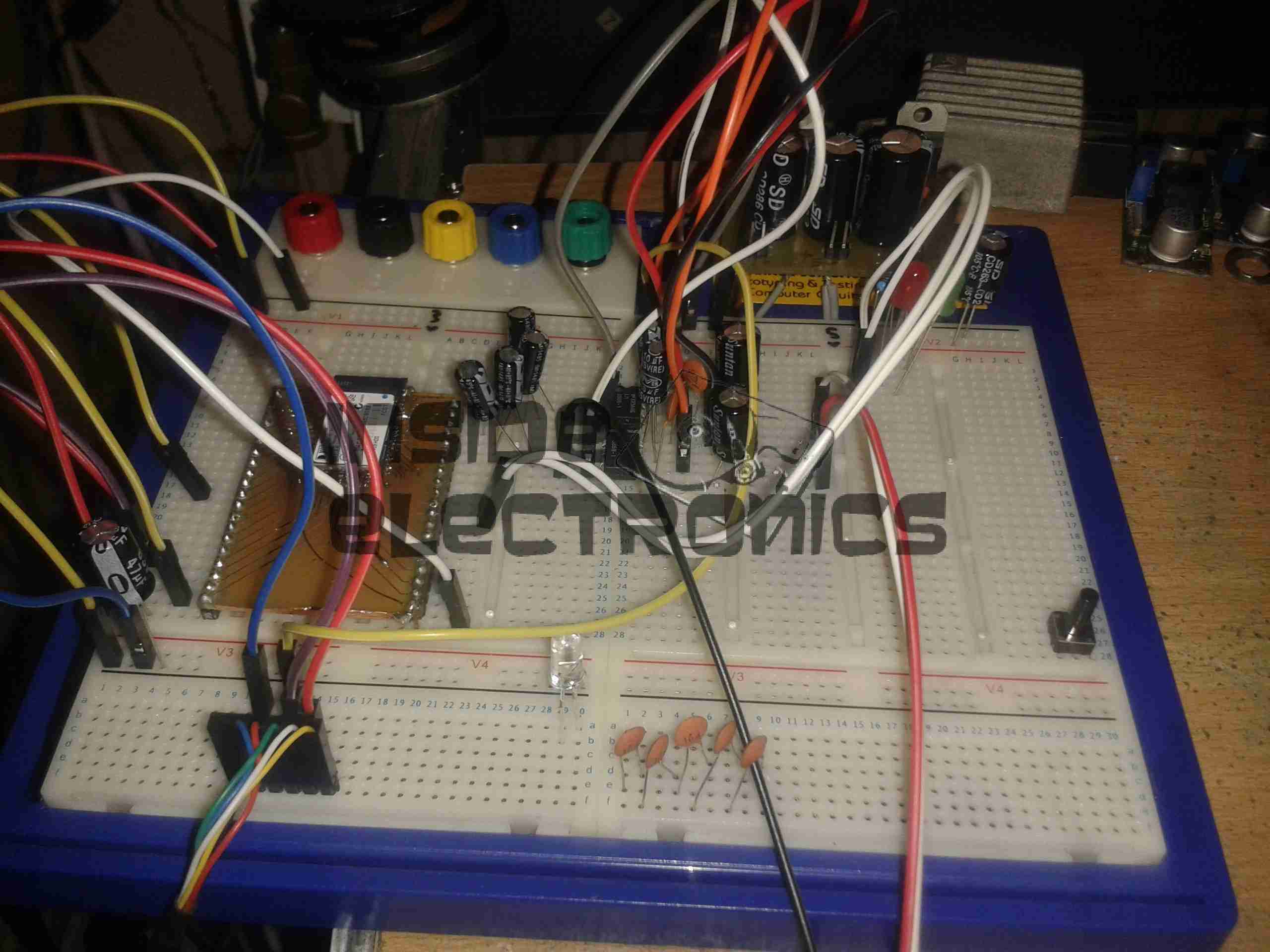
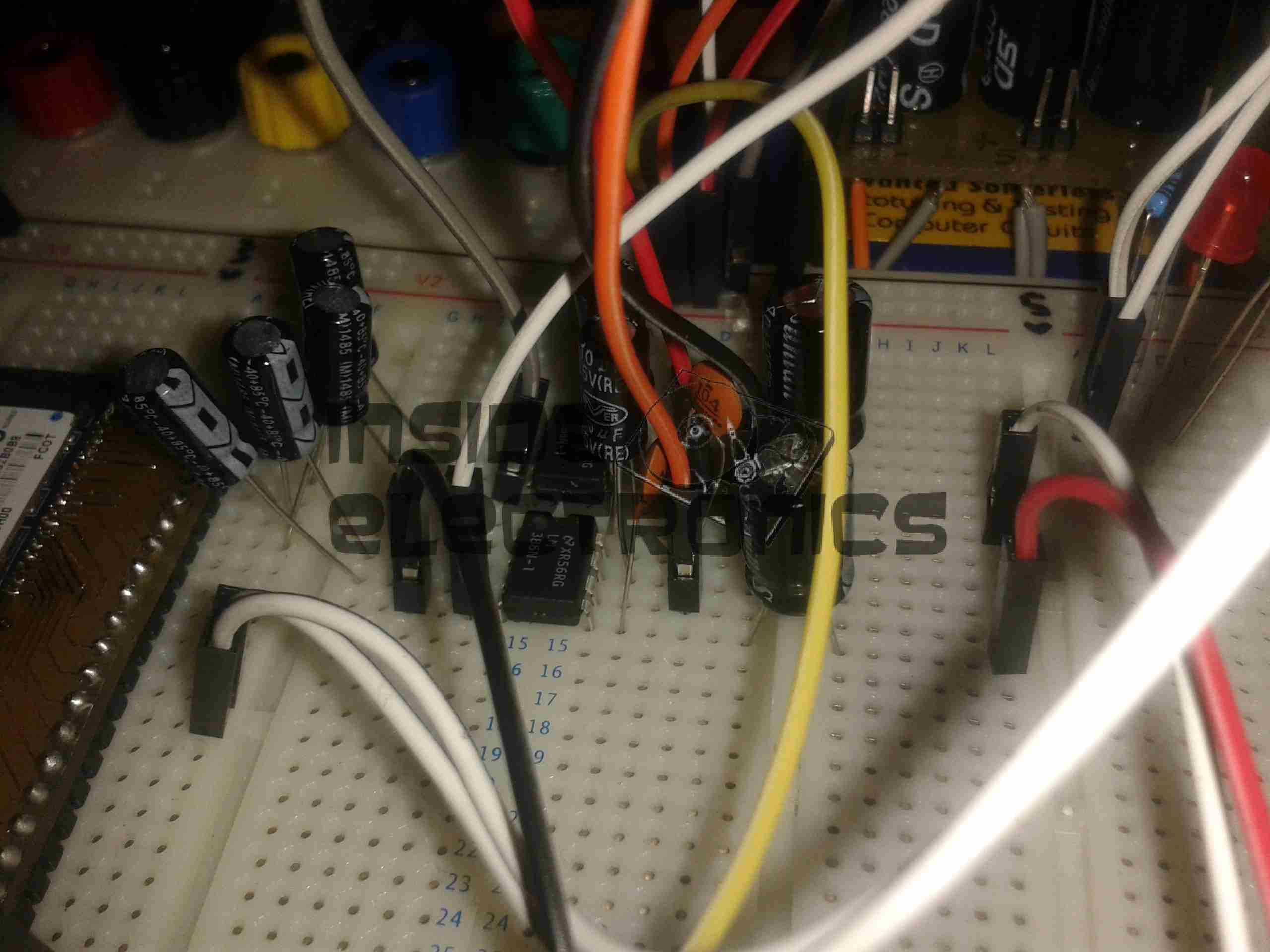
RN-52 Breadboard
Above is the current incarnation of the circuit on the breadboard. The RN-52 is on the left, audio power stage in the centre & headphone output on the right.
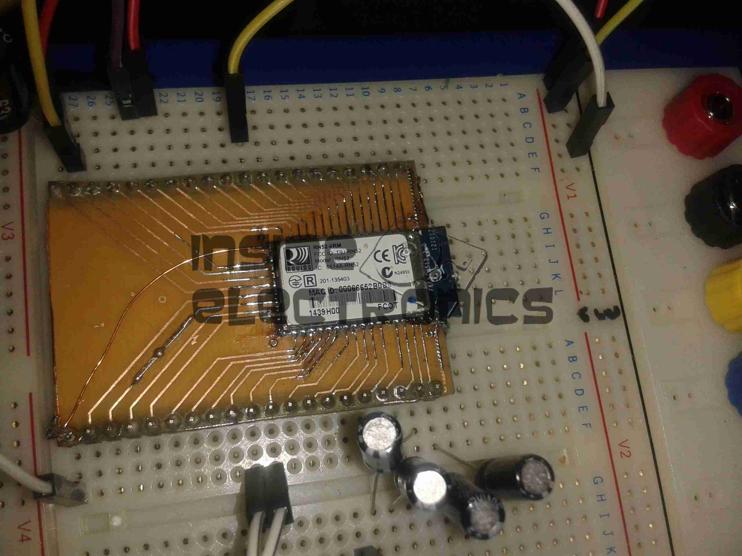
RN-52 Breakout
The bluetooth module on a breakout board. I was cheap in this case & etched my own board. I’m not paying Sparkfun, (as much as I like them), an extra ~£10 for a small PCB with the pins broken out. Much cheaper to spend 15 minutes with the laser printer & the iron, & do a toner transfer PCB.
As this board is single sided, I added a ground plane on the underside with copper foil, to help with the RF issues. Breadboards really aren’t all that good at rejecting noise induced when there’s a 2.4GHz transceiver mounted on them.
LM386 Amplifier
The LM386 audio power stage. The differential inputs from the module are capacitively coupled with 1µF electrolytics. This setup remarkably reduced the noise on the output. I left these at their default gain of 20, as I’ll be connecting another high power amplifier stage to drive large speakers.
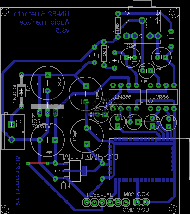
RN-52 Eagle Layout
Here’s the circuit laid out in Eagle, ready for PCB.
RN-52 Eagle PCB
And here’s the PCB layout. Only one link required for the +5v line from the TTL serial port.
As always, the Eagle PCB & Schematic layout files are available at the bottom of the article.
*Update 29-01-15*
Rerouted a few things:
Moved the audio power stage to the +12v rail to improve sound response. – As the LM386 has a max input voltage of 12v (absolute maximum 15v), a regulated supply is recommended. The LM386-N4 variant has a higher voltage range, up to 18v. This should be suitable for an unregulated supply.
Removed 1µF coupling capacitors to reduce distortion & amplifier hiss. The capacitors appeared to cause some instability on the amplifier, causing random distortion. Removing them has cured this. No signal hiss has also been reduced to a very low level.
Reversed input polarity on input of one of the amplifiers – this appears to produce better audio.
Added PWR.EN header to allow connection of power button. Saves hassle of cycling power to the board when the RN-52 goes into sleep mode.
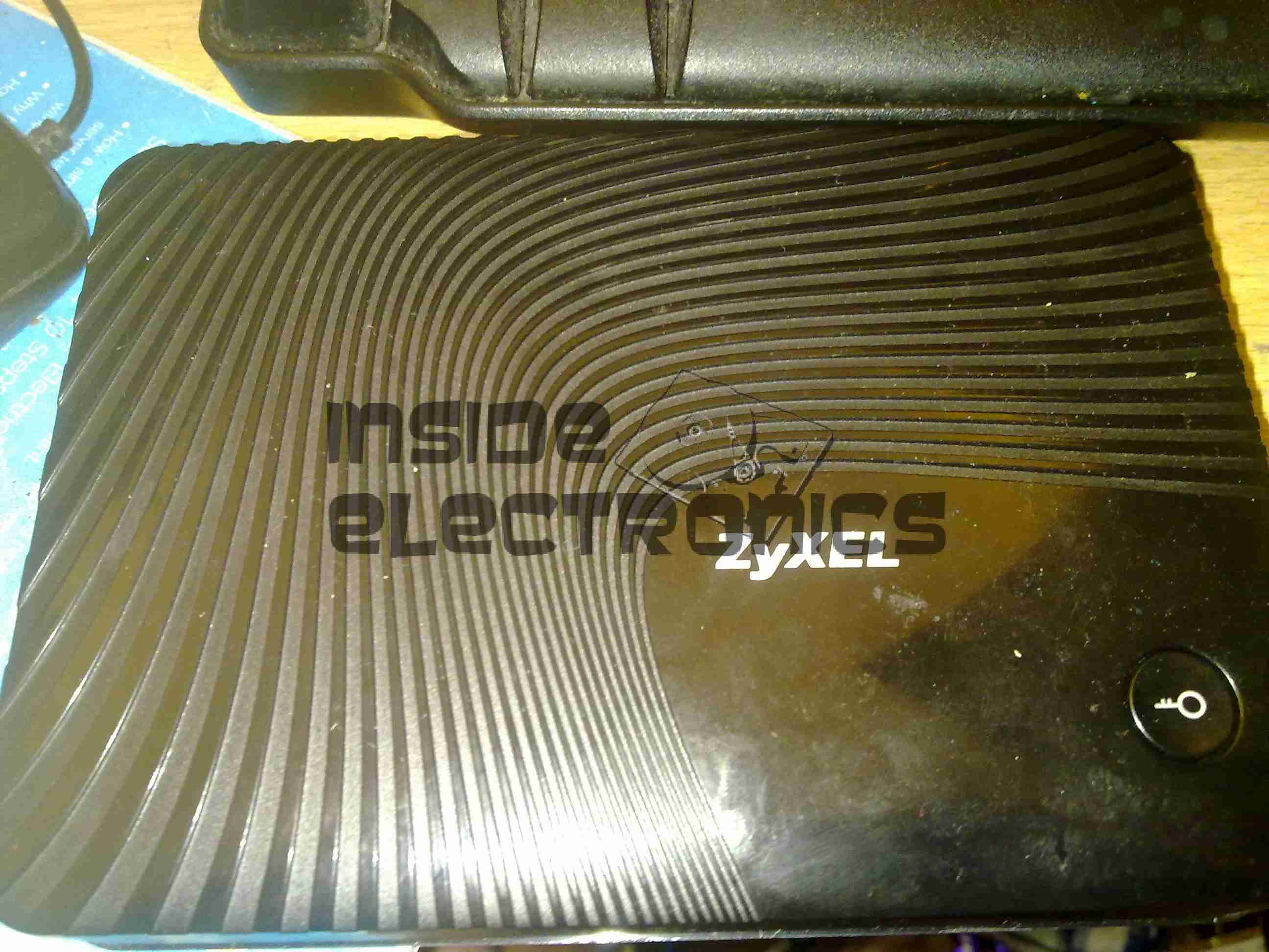
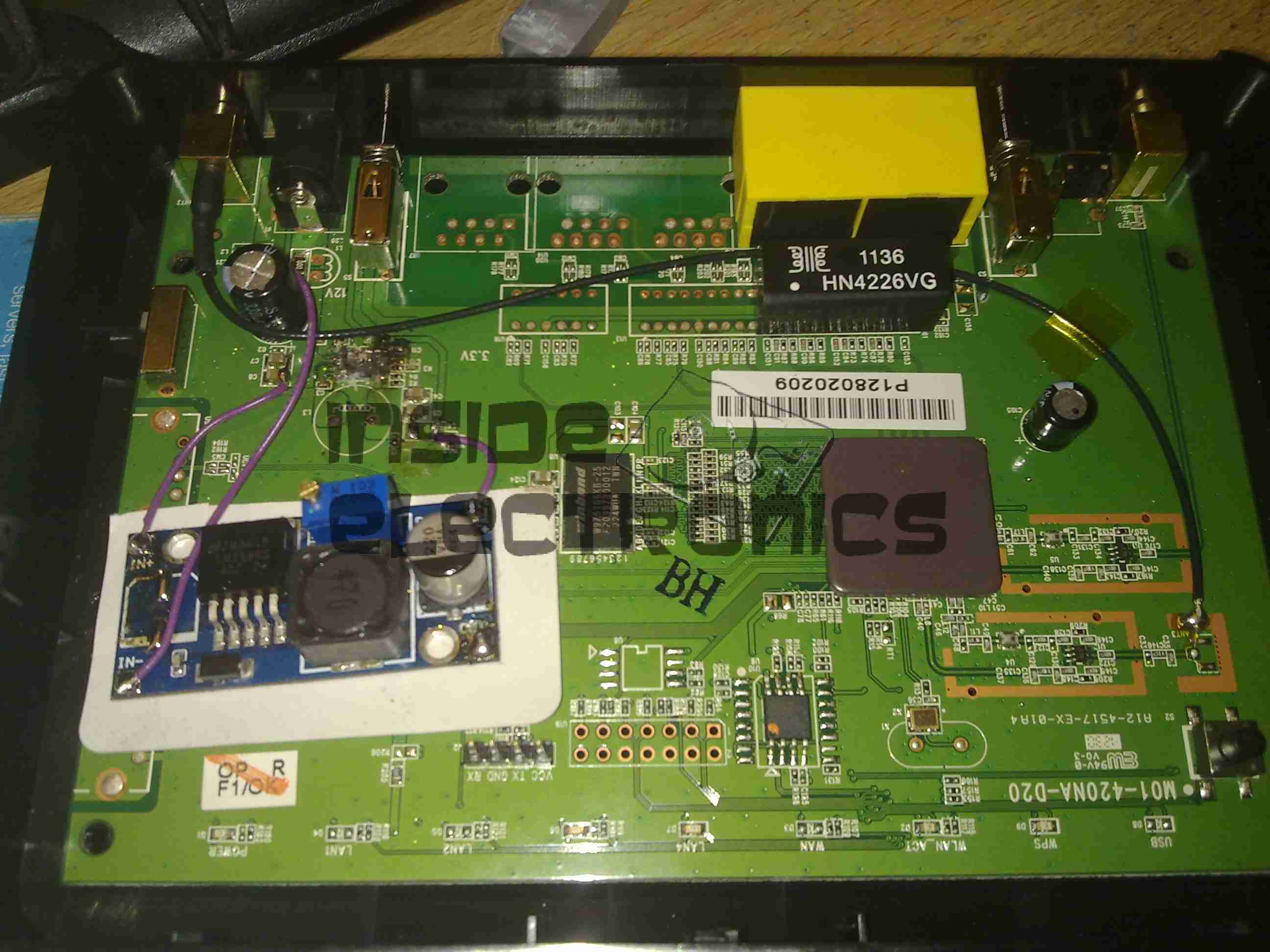
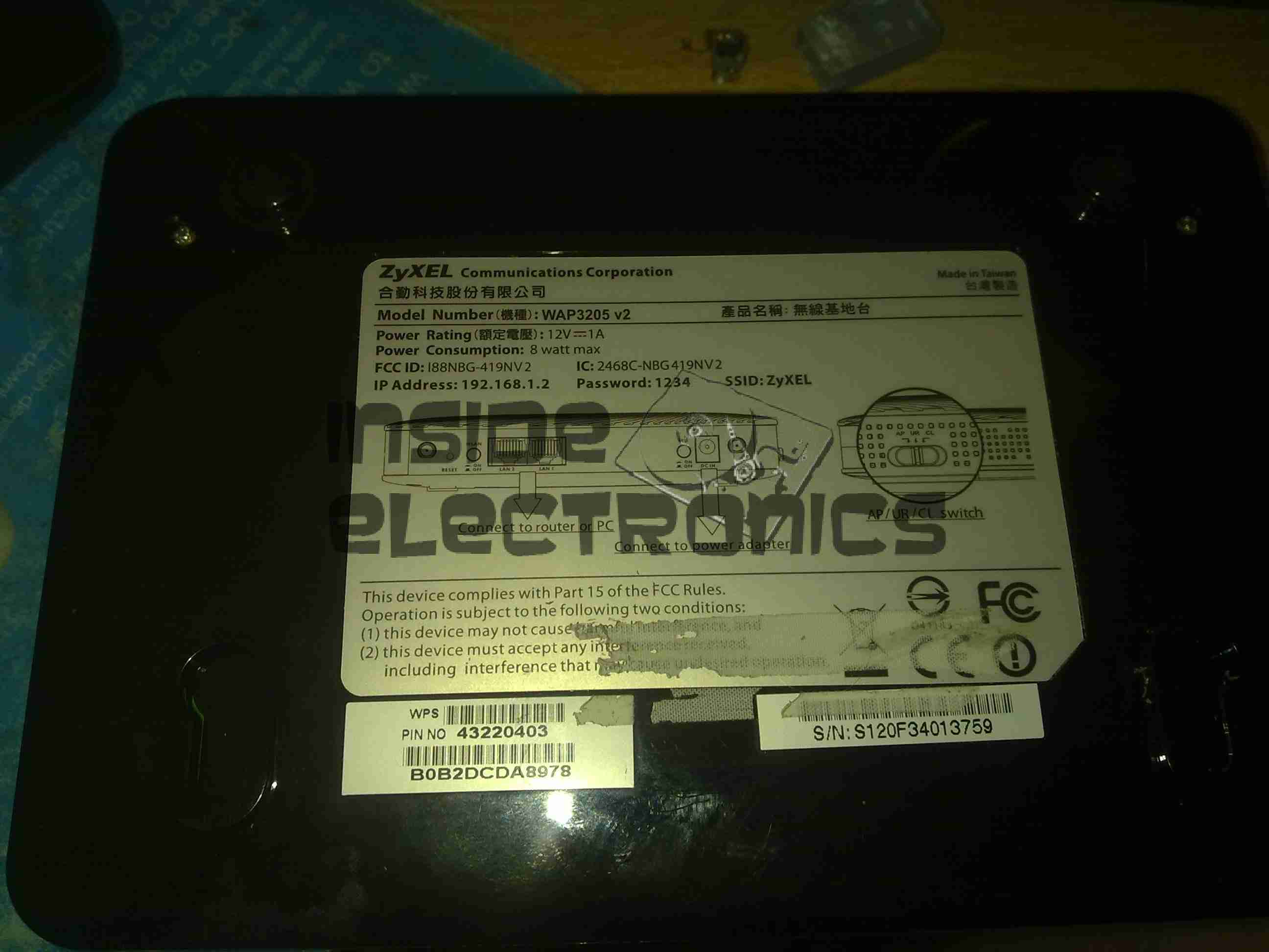
Here is a ZyXel WAP3205 WiFi Access Point that has suffered a reverse polarity event, due to an incorrect power supply being used with the unit.
ZyXEL WAP3205
While most electronic gadgets are protected against reverse polarity with a blocking diode, this unit certainly wasn’t. Applying +12v DC the wrong way round resulted in this:
Blown Switchmode IC (Fuzzy Focus)
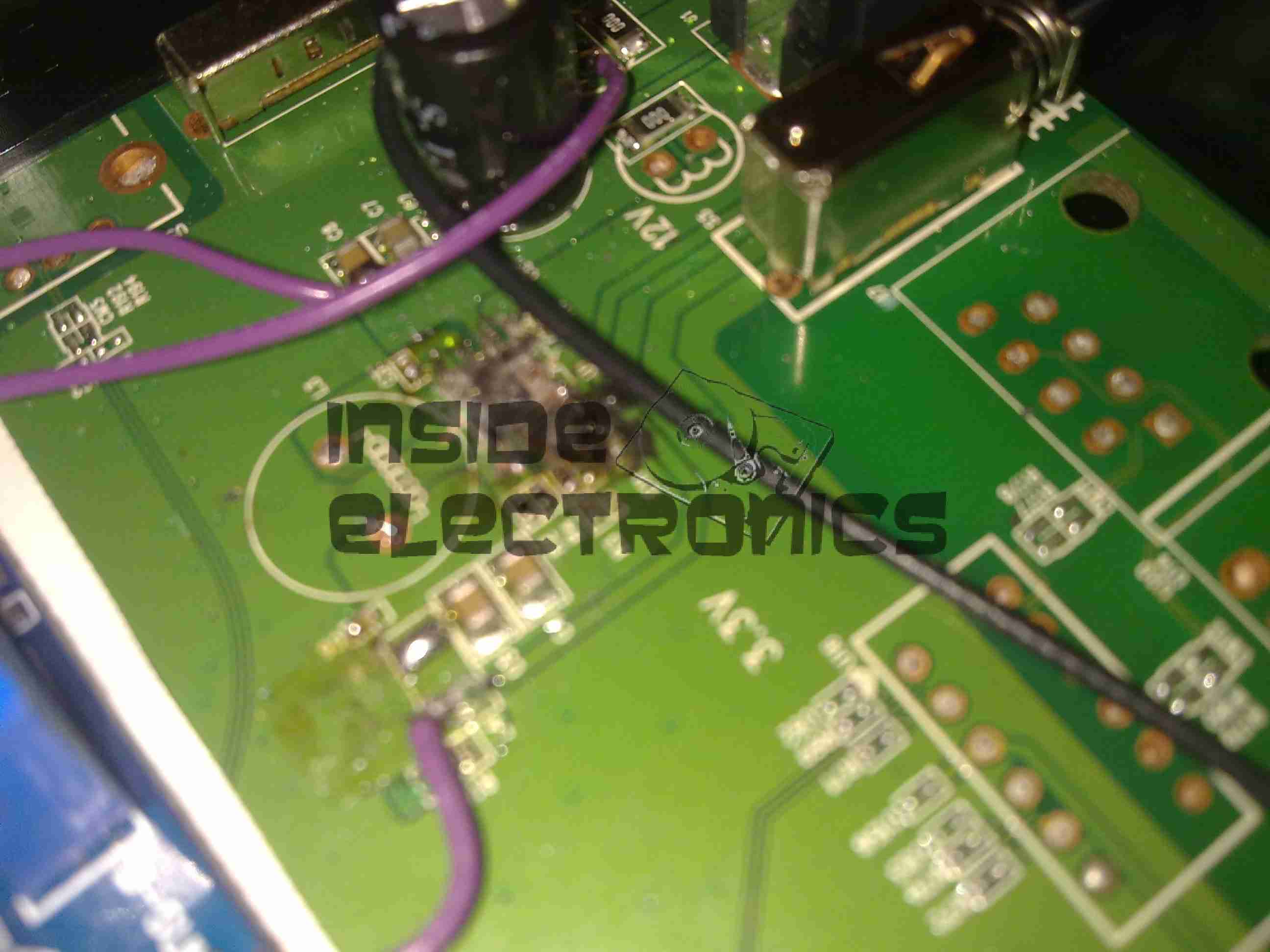
That is the remains of the 3.3v regulator IC, blown to smithereens & it even attempted an arson attack. Luckily this was the only damaged component, & I was able to repair the unit by replacing the switching IC with a standalone regulator. (Replacing the IC would have been preferable, if there was anything left of it to obtain a part number from).
I scraped away the pins of the IC to clear the short on the input supply, removed the switching inductor, & tacked on an adjustable regulator module set to 3.3v. Luckily the voltage of the supply is handily marked on the PCB next to the circuit.
Replacement PSU
Replacement SMPS in place on top of the PCB. The output of the supply is connected to one of the pads of L4 (on my unit just an 0 ohm link), the +12v input is connected to the + rail side of C8 & C7 & the final ground connection is hooked in to the back of the barrel jack.
After this replacement, the unit booted straight up as if nothing had happened. All the logic is undamaged!
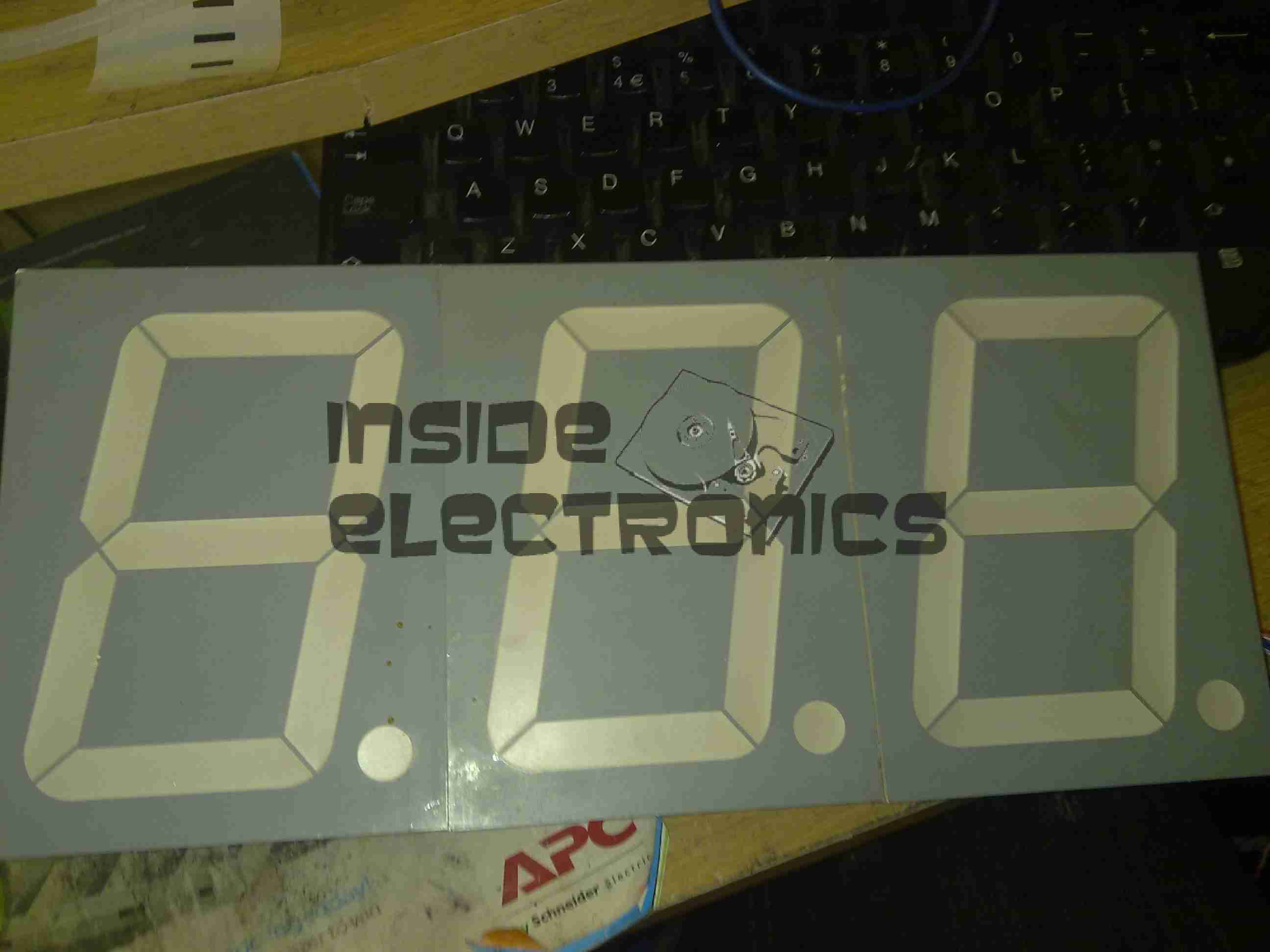
I was recently given some 4″ 7-Segment displays, Kingbright SC40-19EWA & of course, I needed to find a use for them.
I only have three, so a clock isn’t possible…
4″ 7-Segment Display
As these displays are common cathode, & have a ~9v forward voltage on the main segments, some driver circuity is required to run multiplexed from an Arduino.
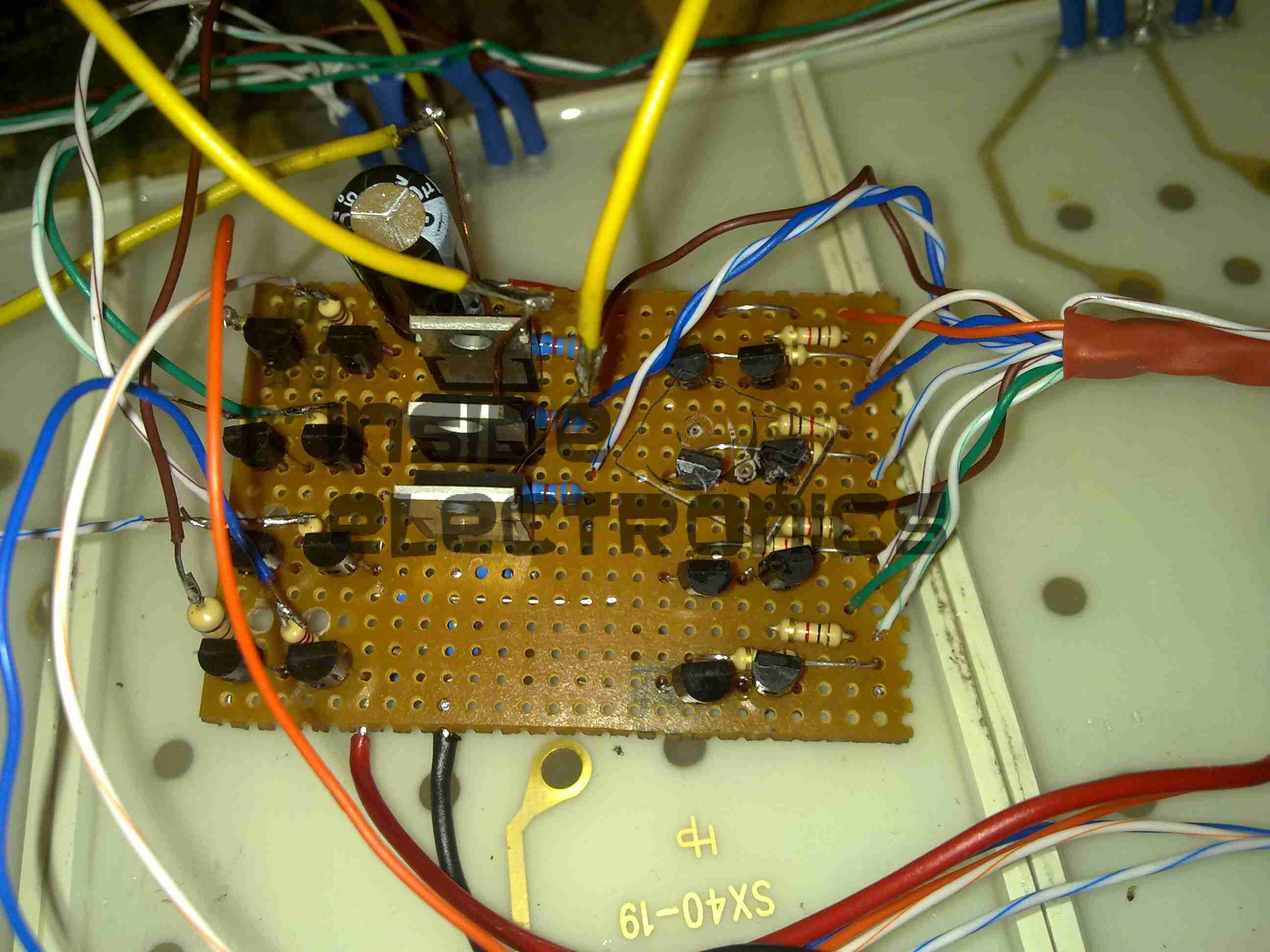
Driver Transistors
Driver circuit built on Veroboard, PNP segment transistors on the left, cathode NPN transistors in the centre, level-shifting NPN array on the right.
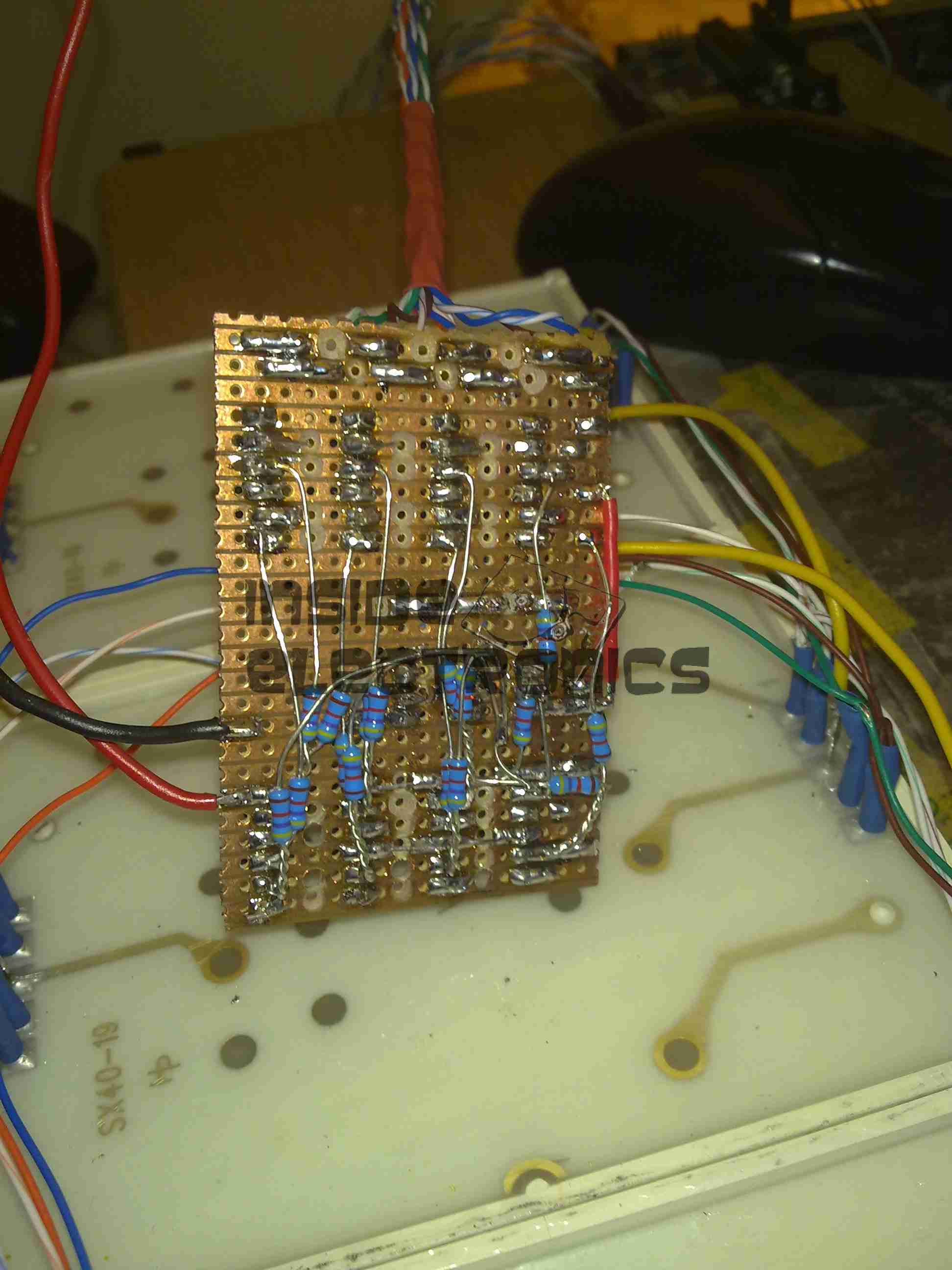
Base Bias Resistor Network
Base bias resistors on the back of the board to bias the bases of the segment drive transistors correctly.
Display Rear
Board soldered into the pins of the displays, which have been multiplexed.
Schematic to come along with some Arduino code to run a room thermometer, with an LM35 sensor
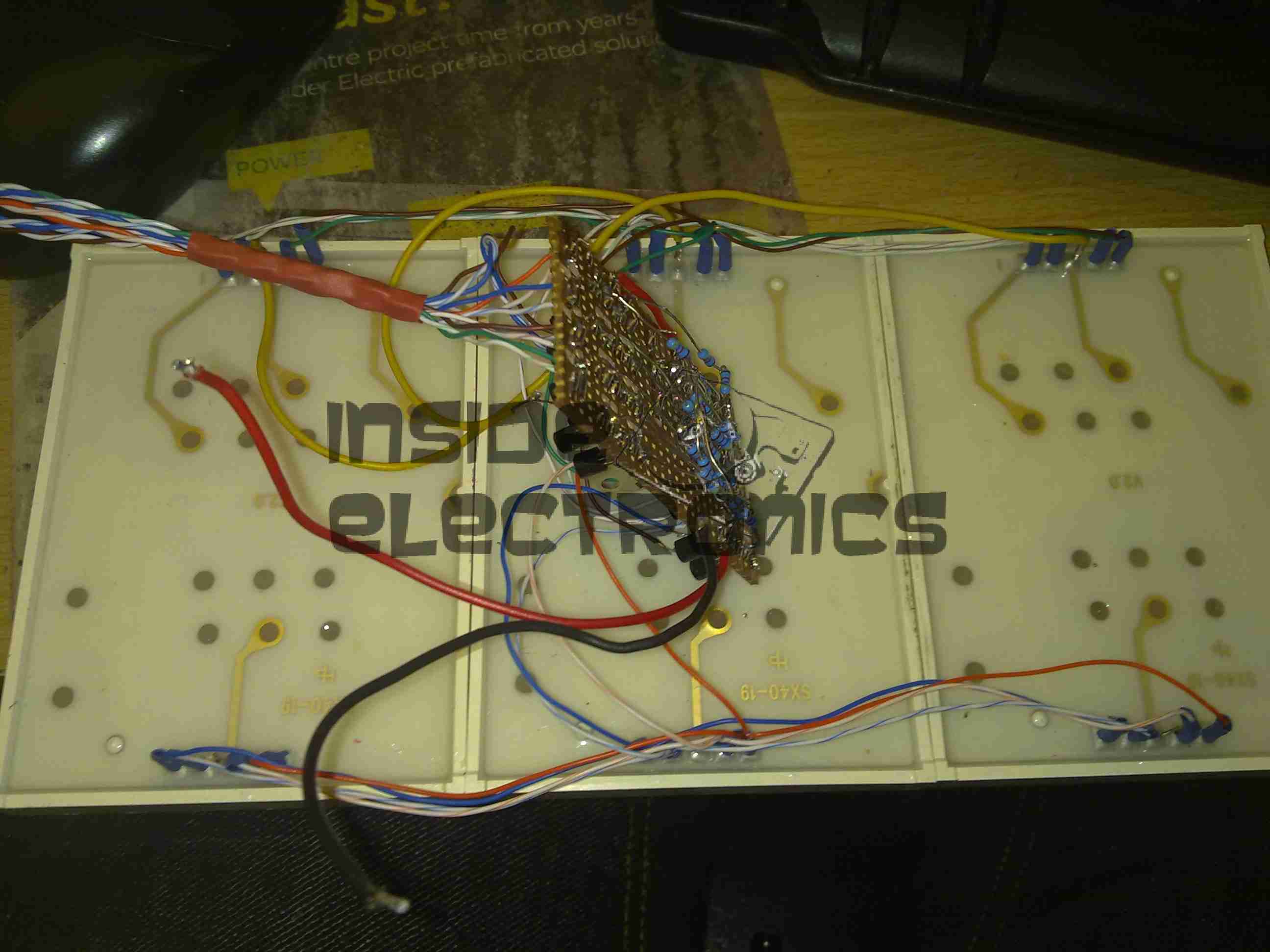
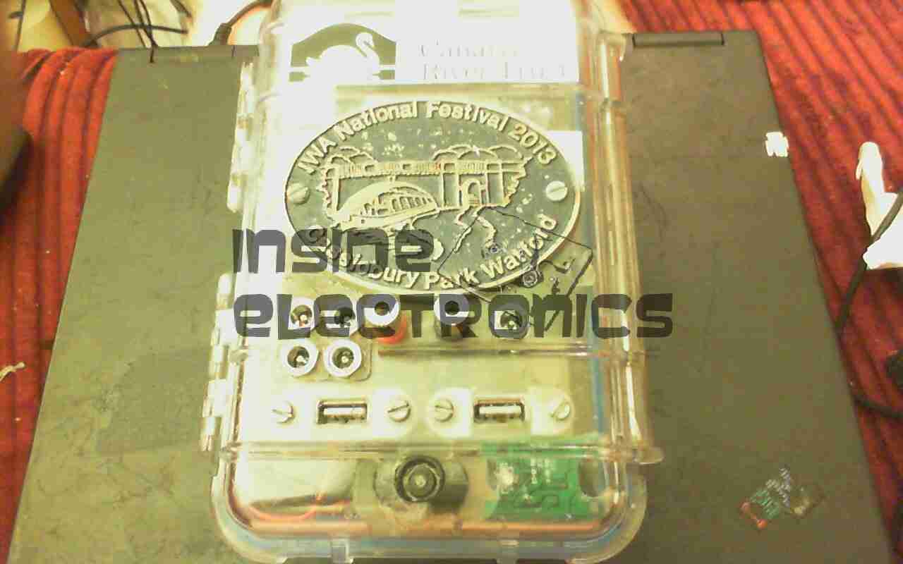
After 13 months of very heavy use at various events, festivals & boat trips, the Li-Po battery pack at the heart of my portable power supply has died.
What initially started as one cell inflating spread to the other cells in the pack over a period of about 3 months, so I have completely replaced the pack with a larger unit.
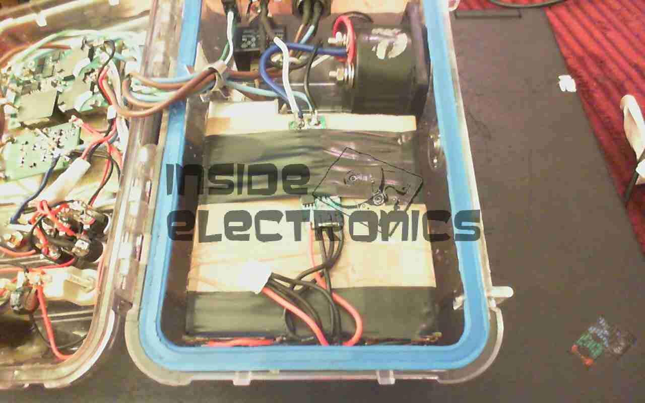
New Pack
The old pack was an 8.8Ah unit at 12.6v. By using smaller burst capacity cells, I have managed to squeeze in a total of 13.2Ah, still leaving space to spare for an extra 3 cell string along the top.
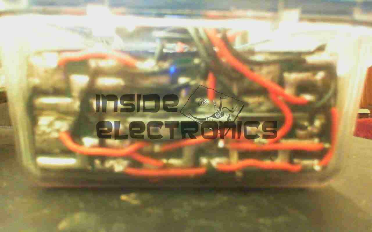
Cell Interconnects
Here is the end of the battery pack, with all the cell interconnects. There are 3 2.2Ah cells in series to give the 12.6v terminal voltage, with 6 of those strings in parallel to give the total Ah rating.
A new charging circuit will be implemented to better handle the volatile chemistry of Li-Po cells, hopefully this will result in the pack lasting longer than a year!
The new higher capacity will hopefully help with power requirements at future events, still being charged during the day by a 24W solar panel, but at night will have to cope with charging two smartphones, two eCigs & running a few watts of LED lighting.
The trial-by-fire will be this year’s Download Festival in June, when I will be operating off-grid for 6 days.
The quickest project from inception to working PCB yet:
From inception to a working PCB took only 4 hours!
LM386 Amplifier
This is a miniature stereo audio amplifier, 0.5W per channel, that can be run from any voltage between 4-12v DC.
As usual, all the Eagle project files are available for download below & kits/bare PCBs will be available for sale for those that cannot etch boards.
In Operation
Here is the circuit driving a pair of 3W 8Ω speakers from a line level audio source. The gain of this circuit is set at 50 with the components specified.
Schematic
As can be seen from the schematic, this is a pair of single LM386 ICs for each channel.
I received this USB supply with a laser module from China that I purchased on eBay. I have heard of these nasty copies of Apple chargers going around, but I’d never received one this bad with a piece of Chinese electronics.
Label
Model No. A1265, so definitely an Apple clone. Apparently capable of +5v DC 1A output. Notice the American NEMA pins. This wouldn’t have been any use to me in the first instance since I am resident in the UK & our mains plugs are significantly different, not to mention significantly safer.
Manufacturer is marked as Flextronics.
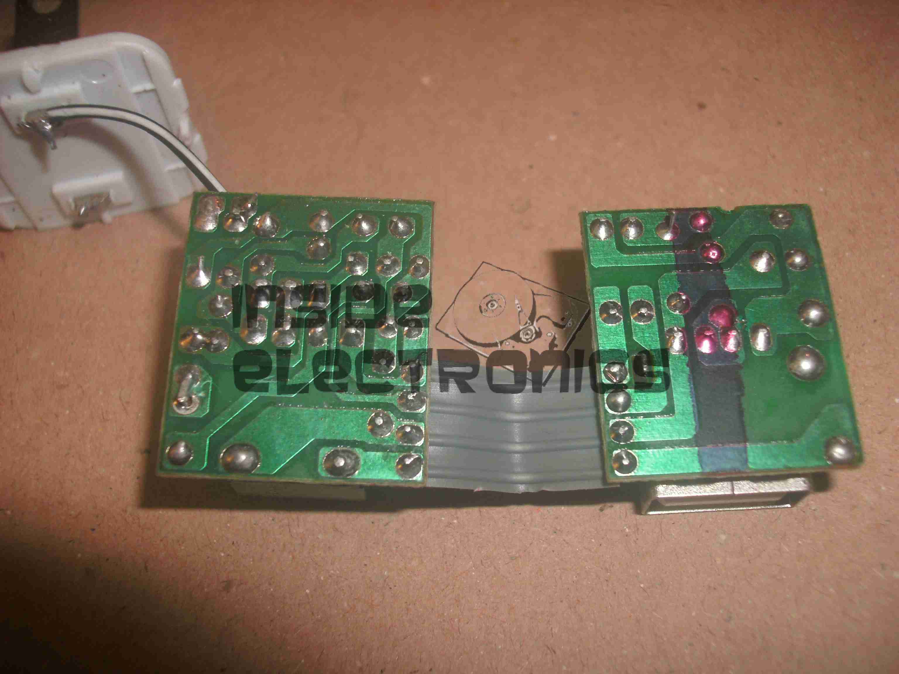
Top Of Boards
Here is the charger disassembled. Inside the case these two boards are folded together, creating an alarmingly small isolation gap between the mains side of the supply & the 5v output. Both the low voltage output & the feedback loop for the supply runs over the 4-core ribbon cable.
The mains wiring from the board is as thin as hair, insulation included, so there is a big possibility of shorts all over the place from this part of the circuit alone.
Bottom Of Boards
Bottom of the PCB assemblies. Good luck finding any creepage distance here. There simply isn’t any at all. traces on the +350v DC rail on the mains side of the transformer are no more than 1mm away from the supposedly isolated low voltage side.
Plugging one of these devices into anything is just asking for electrocution.
Tip Jar
If you’ve found my content useful, please consider leaving a donation by clicking the Tip Jar below!
All collected funds go towards new content & the costs of keeping the server online.