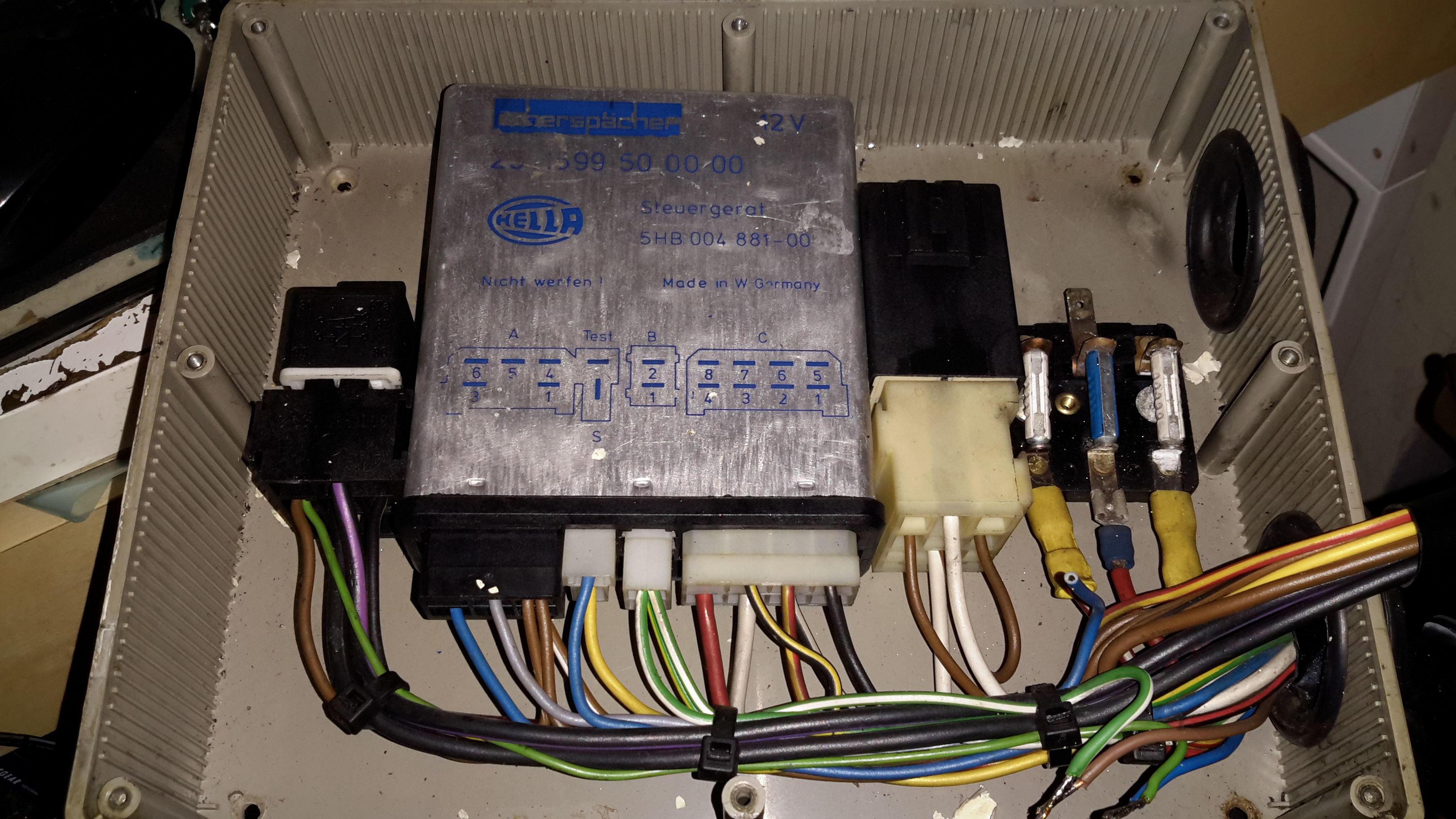
Here’s another Eberspacher control unit, this time from an ancient D5W 5kW water heater. The system in this case is just flaky – sometimes the heater will start without fault & run perfectly, then suddenly will stop working entirely.
The error codes are read on these very old units via an indicator lamp connected to a test terminal. In this case the code was the one for Overheat Shutdown.
Considering this fault occurs when the heater is stone cold, I figured it was either a fault with the sensor itself or the ECU.
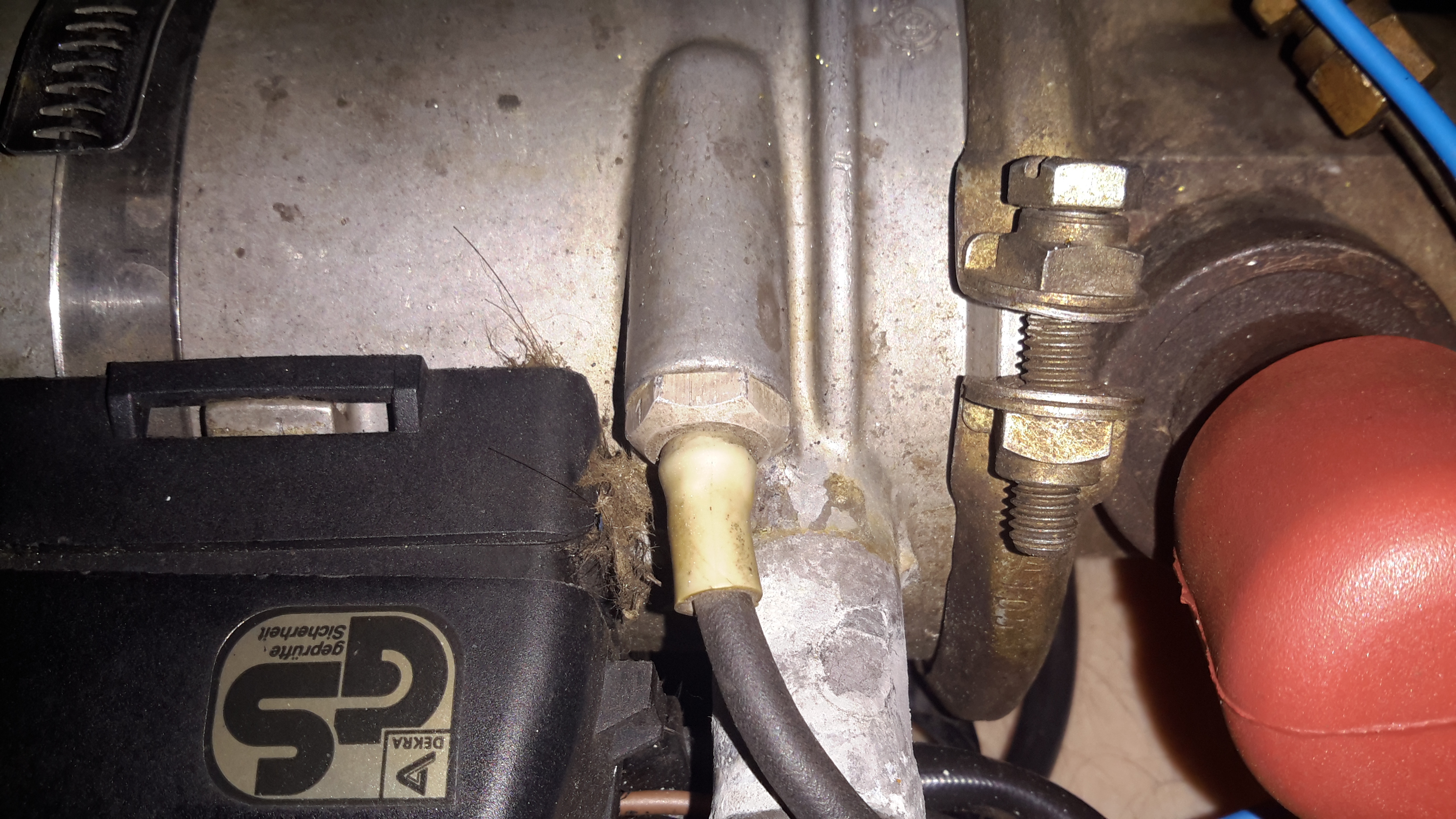
Temperature Sensor
The temperature sensor is located on the heat exchanger, right next to the hot water outlet fitting. I’m not sure what the spec is, but it reads exactly 1KΩ at room temperature.
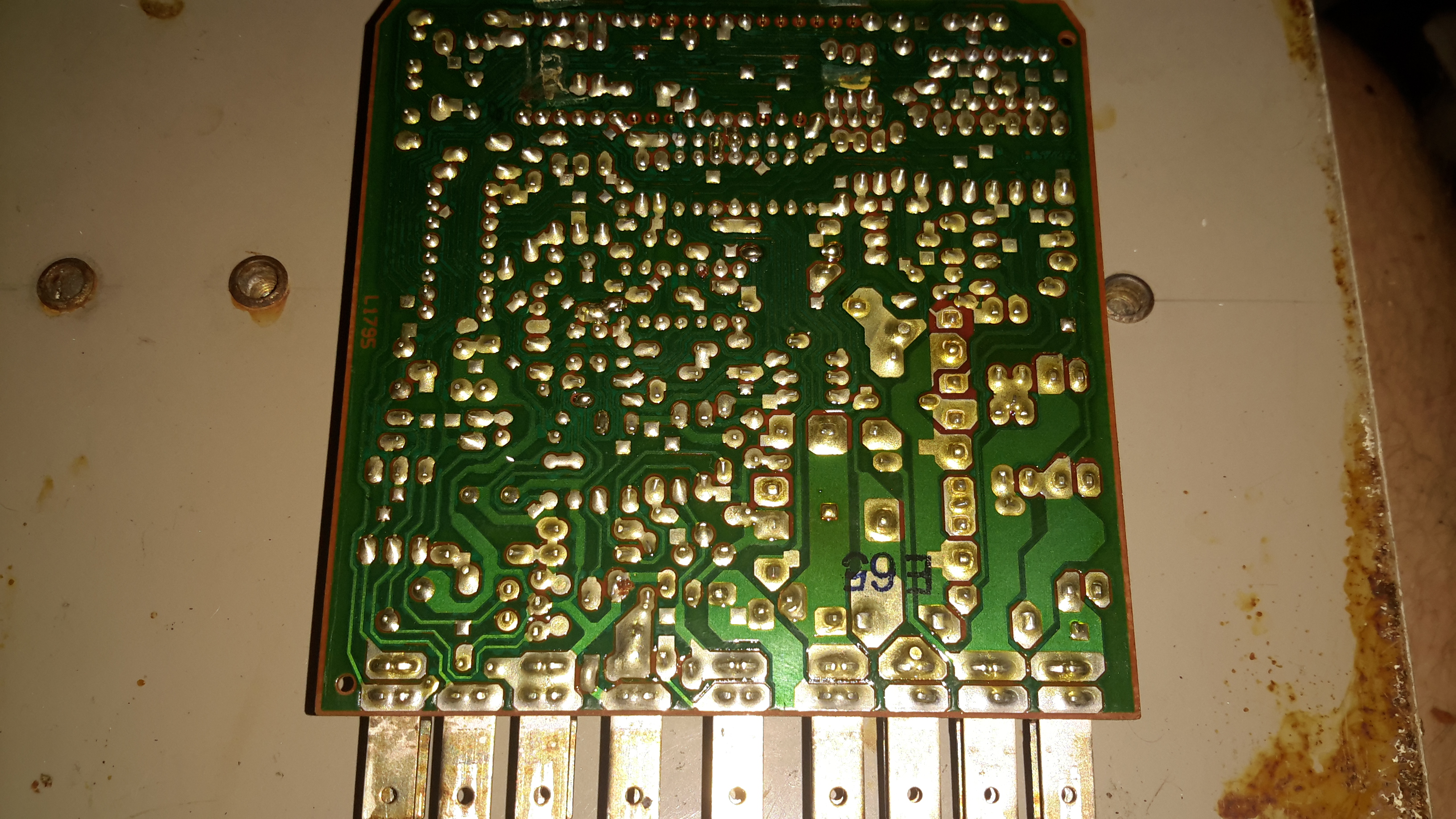
ECU PCB
The PCB is held into the aluminium can by means of crimps around the edge that lock into the plastic terminal cover. Inserting a screwdriver & expanding the crimps allows the PCB to be slid out.
Casing Crimps
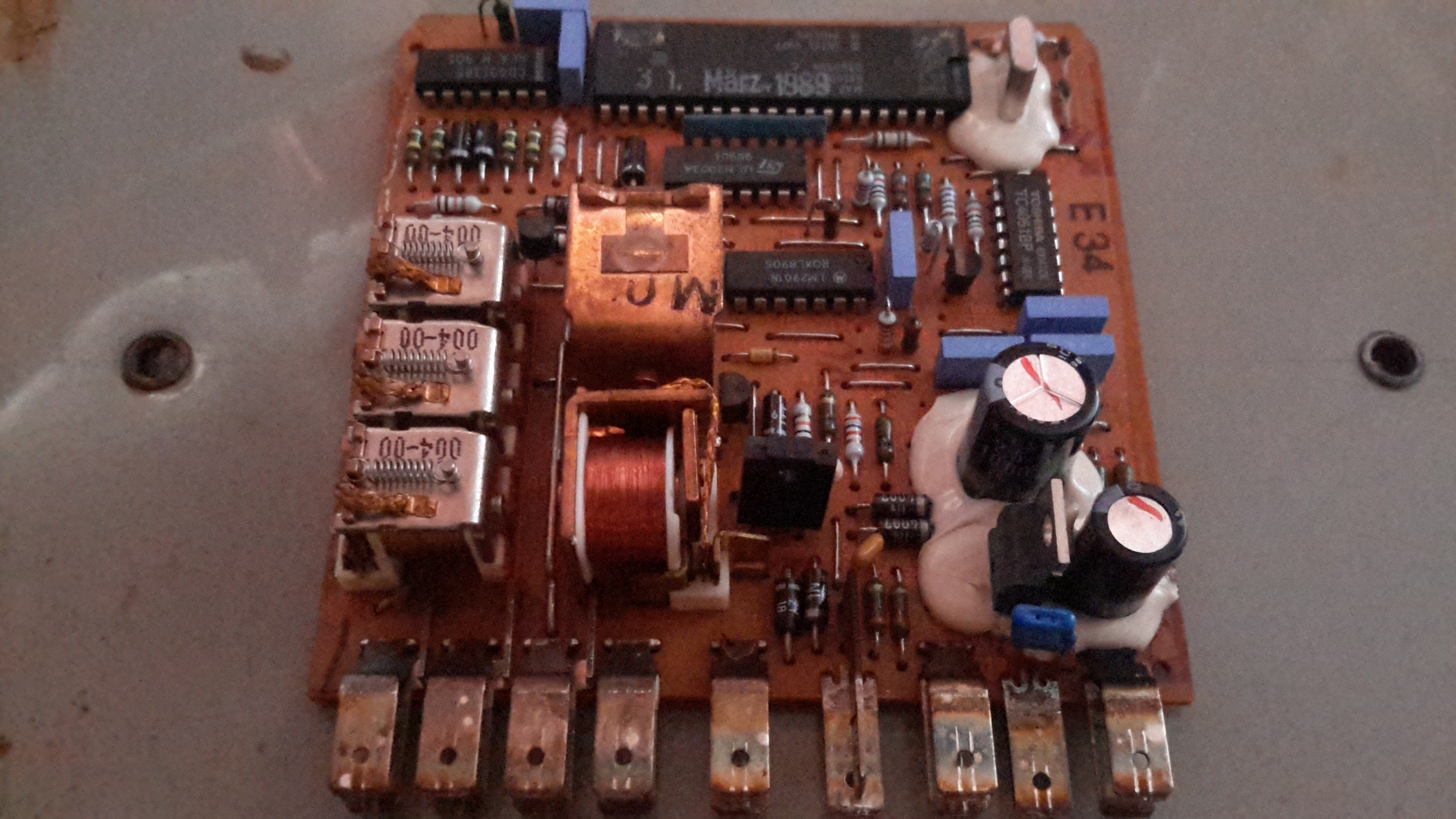
The factory date stamp on the microcontroller dates this unit to March 1989 – considerably older than I expected!
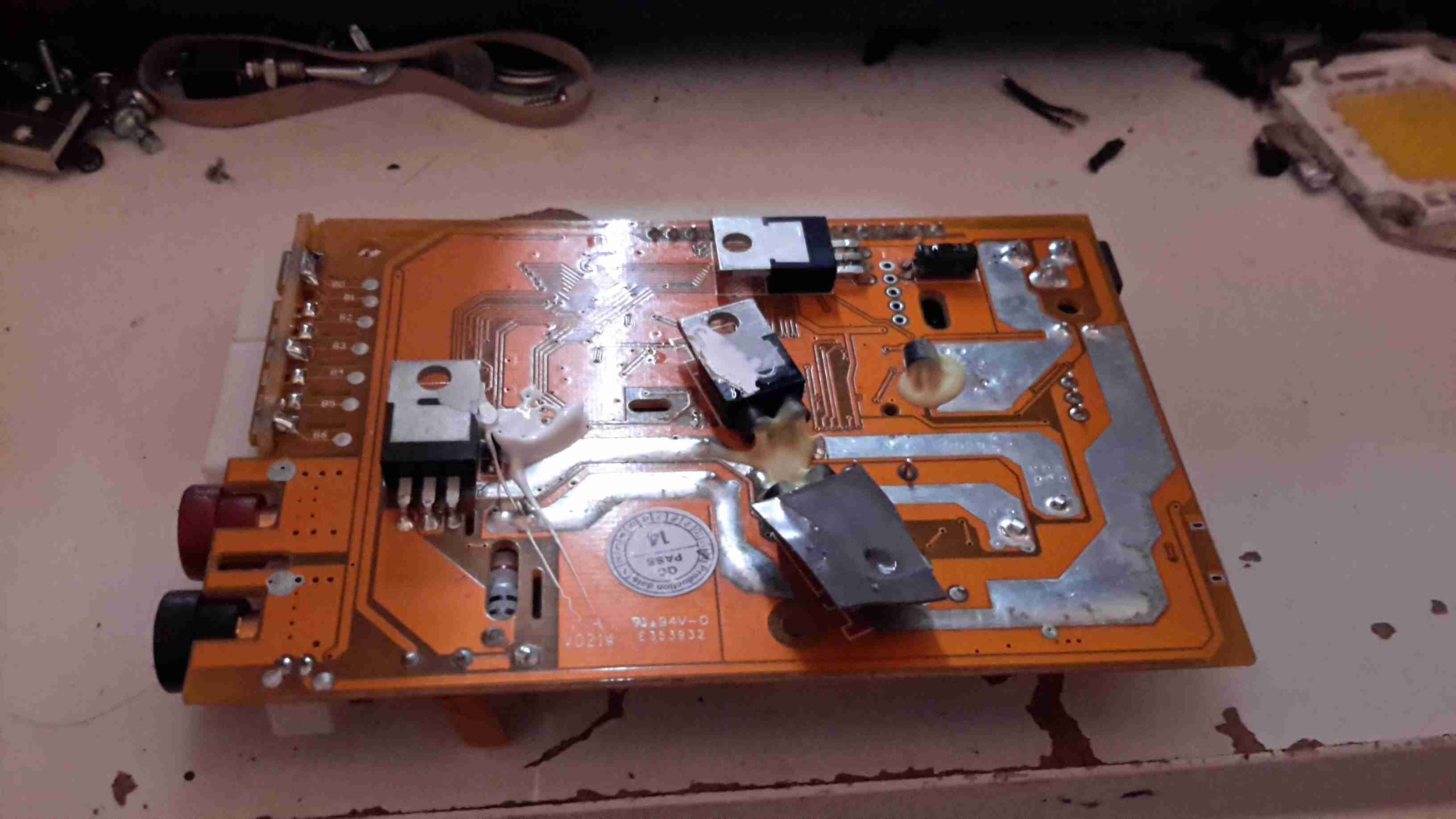
Unlike the newer versions that use transistors, this ECU has a bunch of PCB relays to do the high current switching of the water pump motor, fan motor & glowplug.
Overall the board looks to be solidly constructed, with silicone around all the larger components.
ECU PCB Solder Side
Here’s the solder side of the PCB, which has a generous coating of sealant to keep moisture out.
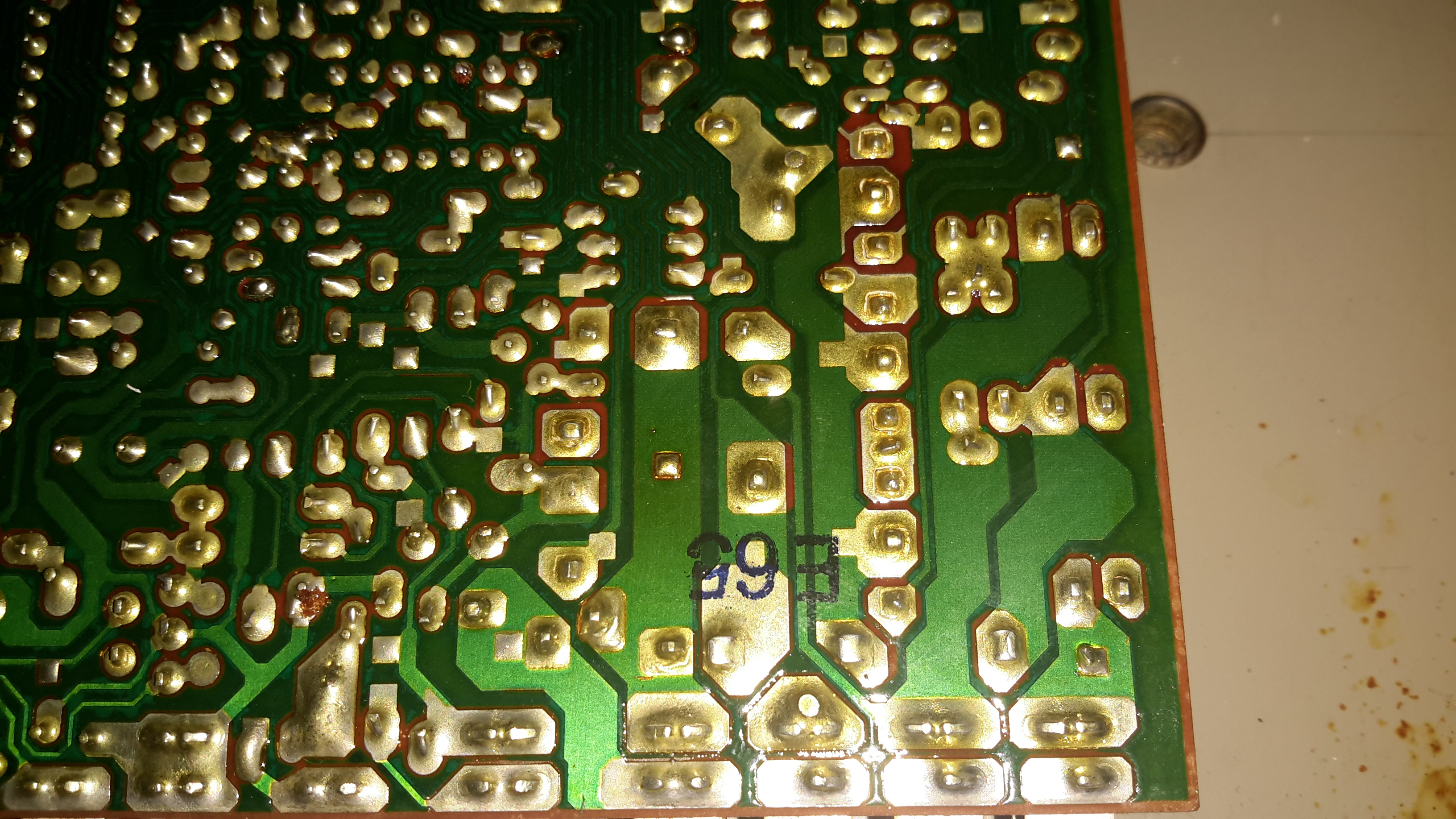
Bad Joint Closeup
Looking at the solder joints for the row of relays on the top side of the PCB, it looks like that there’s some dry joints here.
I suspect that years of vibration has taken it’s toll, as the relays are otherwise unsupported. It wouldn’t be possible to use silicone to secure these devices as they are completely open – any sealant would likely stop them from operating.
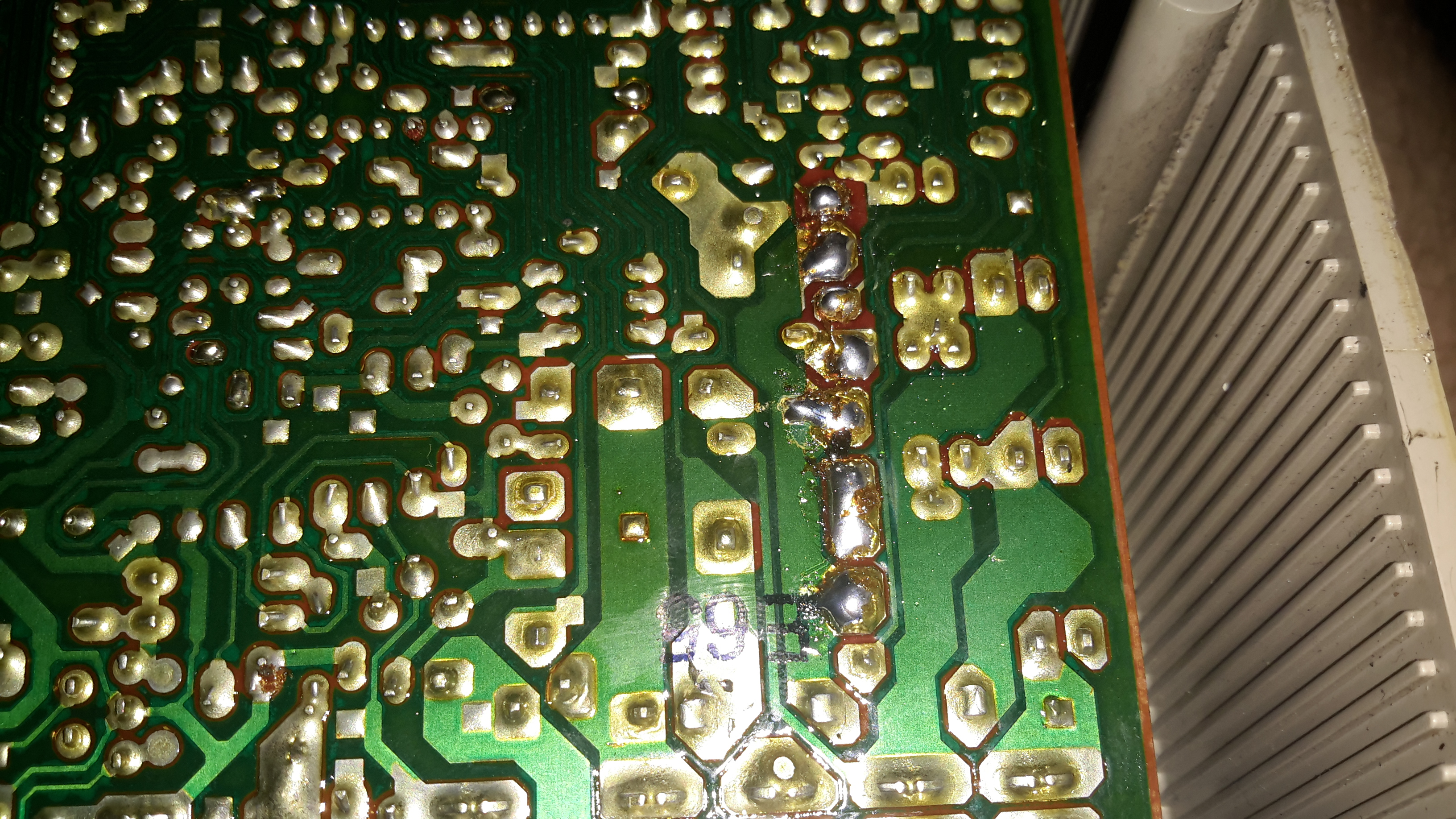
Resoldered Joints
Using a very hot soldering iron I managed to get the joints to reflow properly, using lots of flux to make sure the conformal coating didn’t interfere with the reflow.
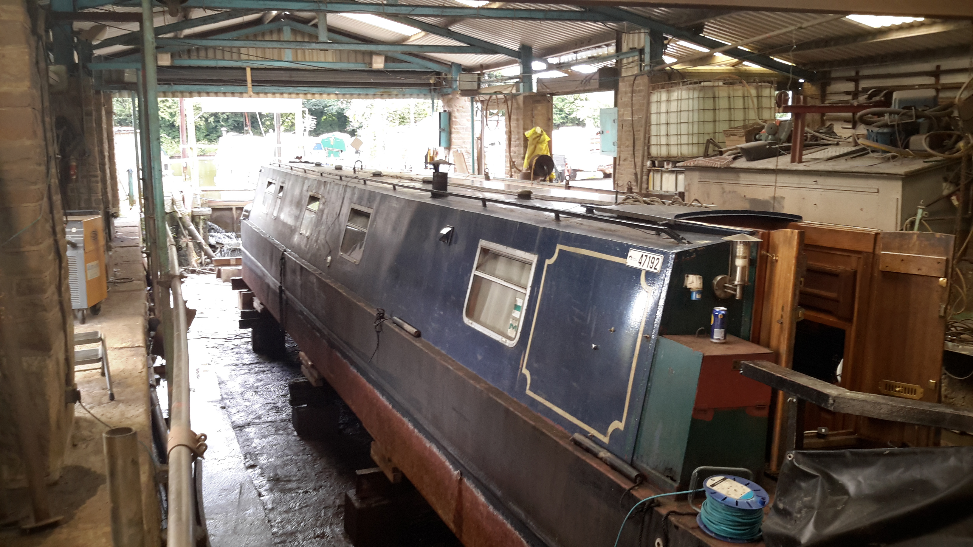
It’s that time again, so the boat is out of the water for it’s 3-yearly maintenance. Some things over the past few months have been bugging me, namely a pronounced vibration in the running gear while underway. (Issue was easy to spot here!).
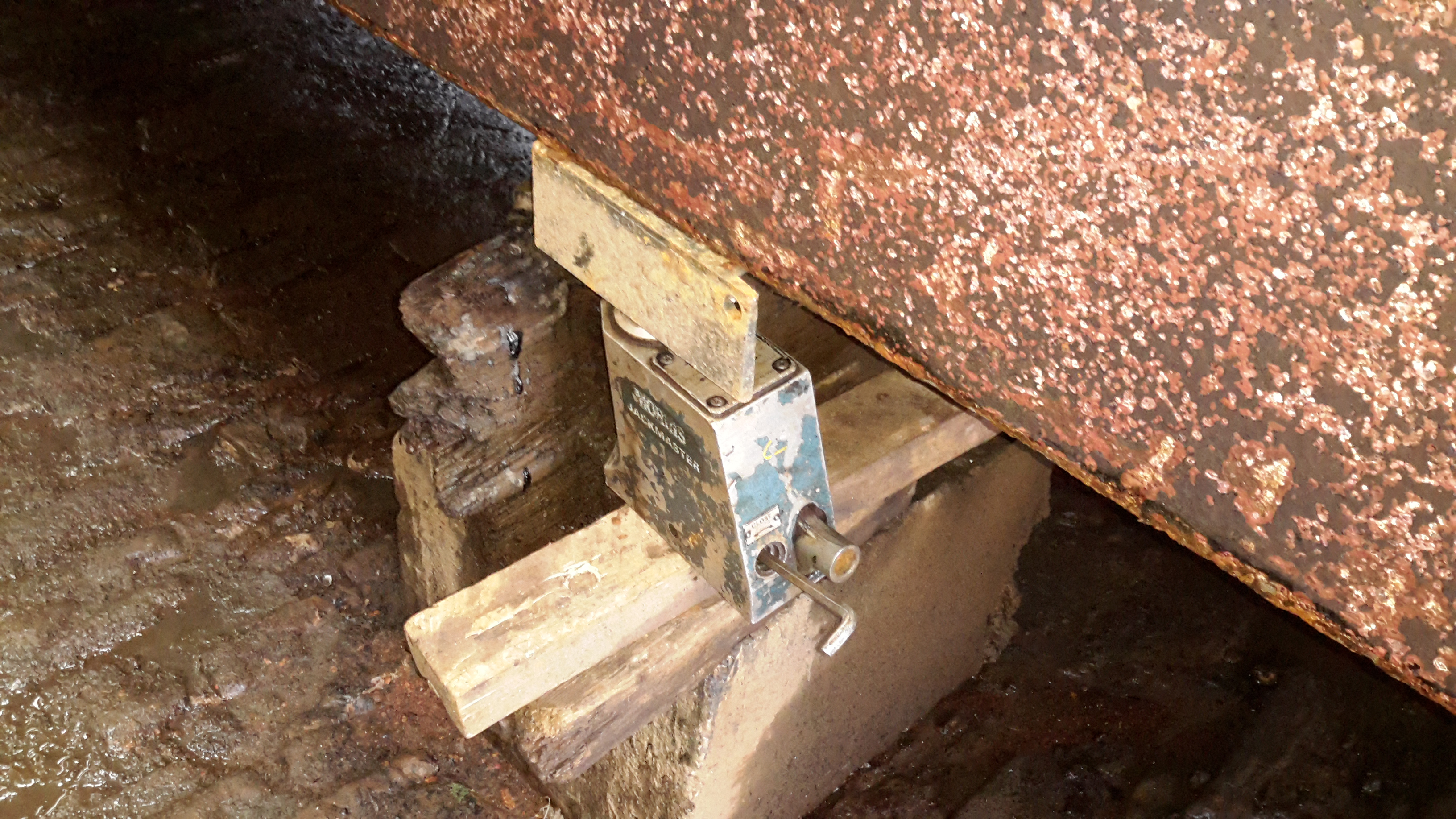
10-Ton Jack
nb Tanya Louise being a very odd vessel, she has quite a significant keel, so once the dock was drained, some manual jacking was required to get her level on the blocks. Without this extra work there is such a pronounced heel that it’s impossible to do anything on board.
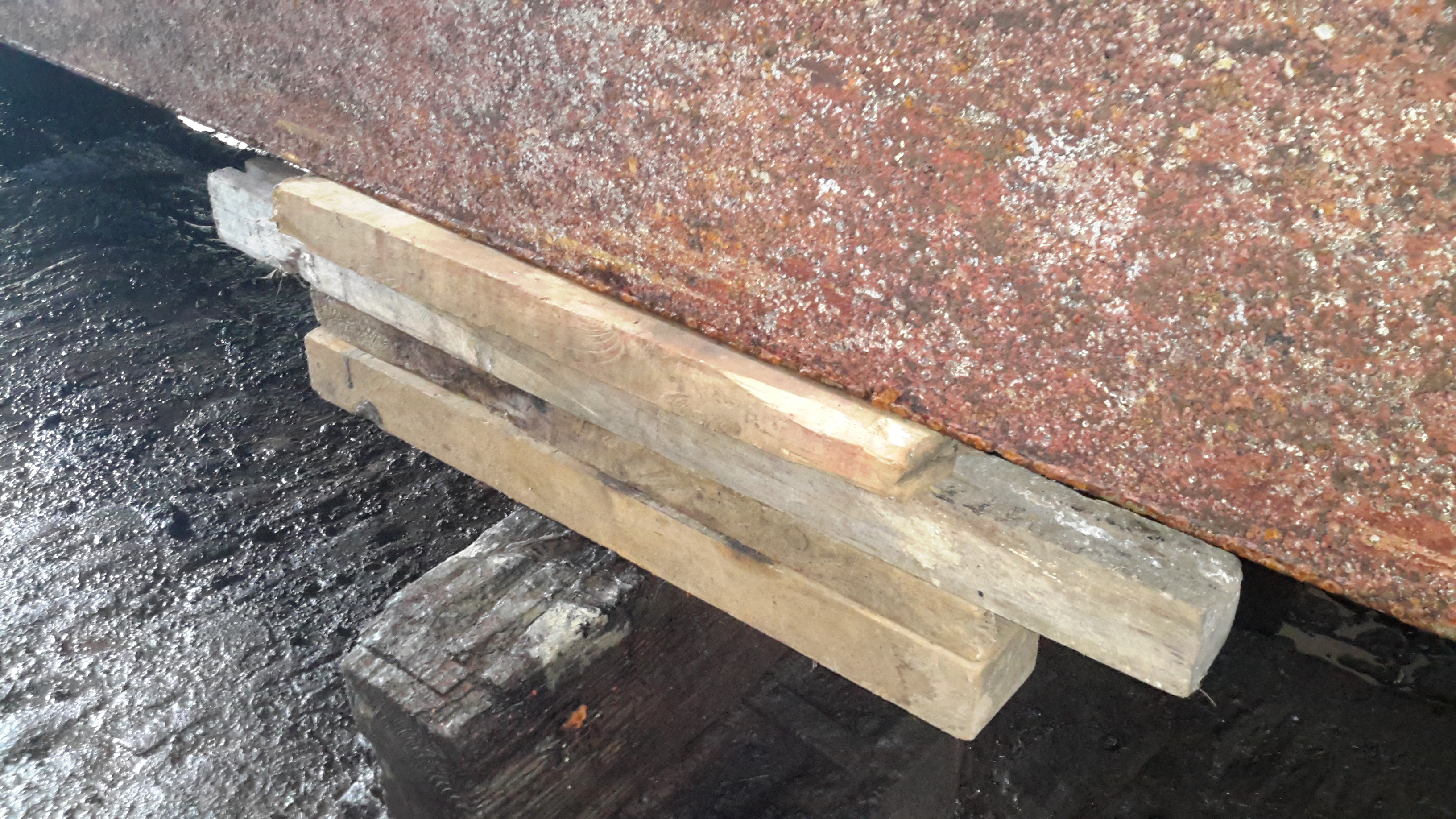
Chocks
On the opposite side, wooded blocks are placed for the bottom of the hull to rest against. Jacking up a 58-ft 25-ton boat by hand onto some timbers was nerve-wracking to say the very least!
The bottom of the hull has already been jet-washed to remove 3-year’s worth of slime, weed growth & the old blacking. First job is to get a fresh coat of paint on.
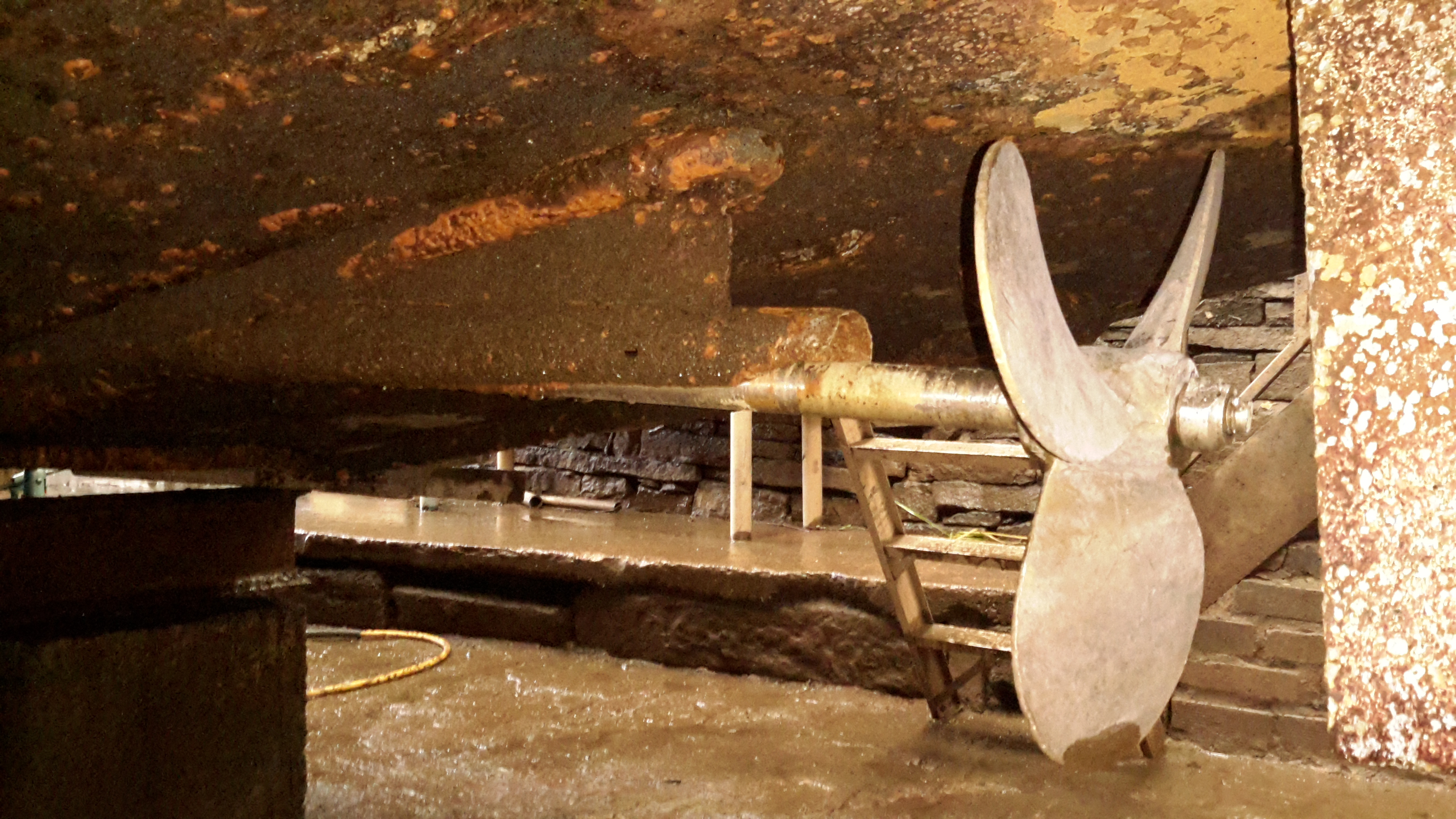
Running Gear
Looking under the hull shows the reason for the high level of vibration – the prop shaft has actually *worn through* the bearing & stern tube, to the extent that there’s not much left of the assembly! The only thing holding the shaft in place at this stage is the stuffing box inside the boat & the shaft coupling to the hydraulic motor.
, stern tube,
A replacement standard-issue Cutless bearing will be fitted, after the remains of the old tube are cut back to make room. To facilitate mounting the bearing, a custom stainless P bracket is being made at a local engineers, for me to weld onto the bottom of the hull.
(Surprised we didn’t lose the shaft, lucky that I kept pestering to get her out of the water!).
To solve some engine oil overheating problems on board nb Tanya Louise, we decided to replace the air-over-oil cooler, with an water-over-oil cooler, with separate cooling drawn straight from the canal, as the skin tanks are already overloaded with having to cope with not only cooling the engine coolant, but also the hydraulic system oil as well.
These units aren’t cheap in the slightest, but the construction quality & engineering is fantastic.
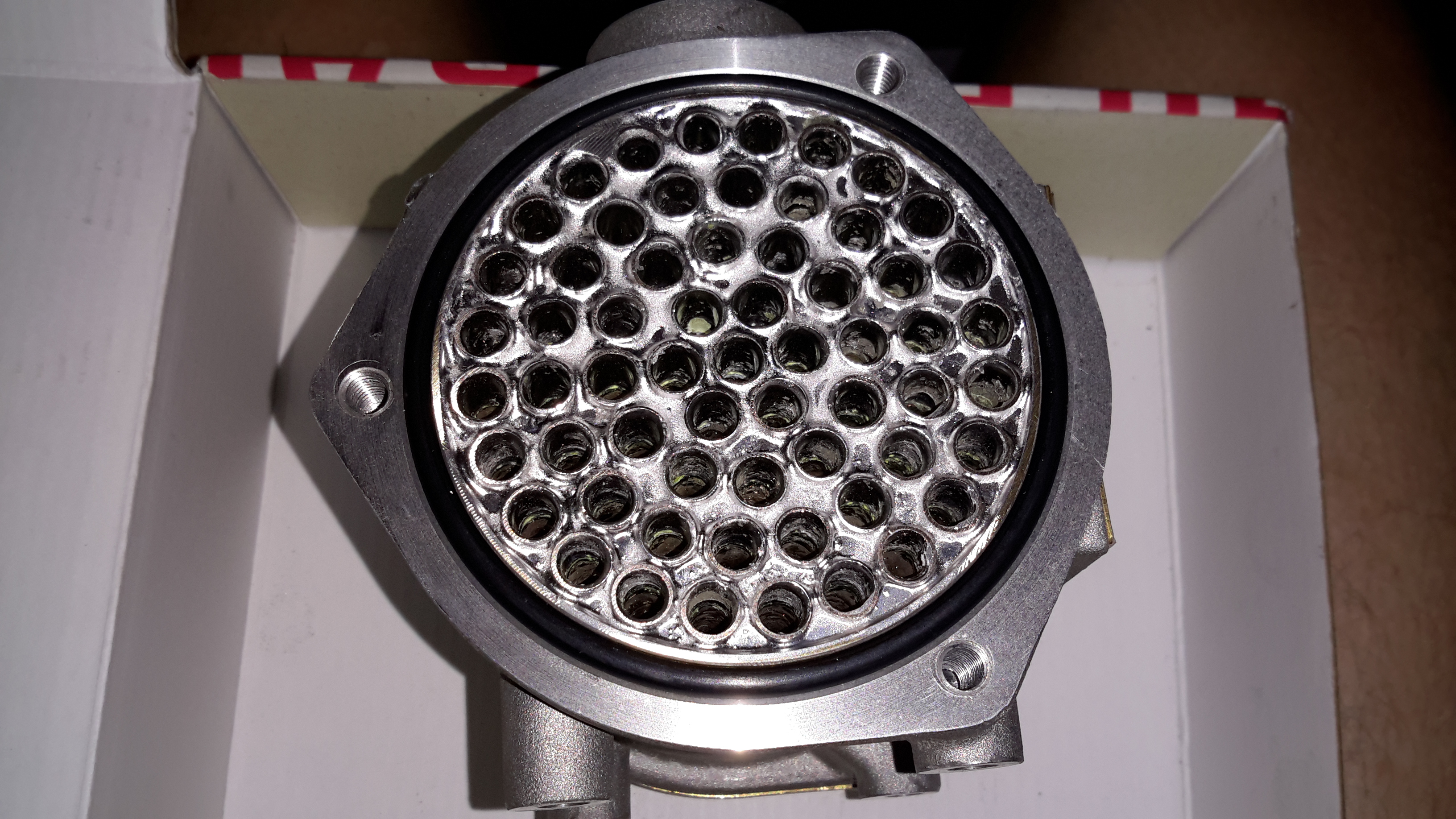
Tube End Plate
Unbolting the end cover reveals the brass tube end plate, soldered to all the core tubes in the cooler. An O-Ring at each end seals both the end cover & the interface between the tube plate & the outer casing.
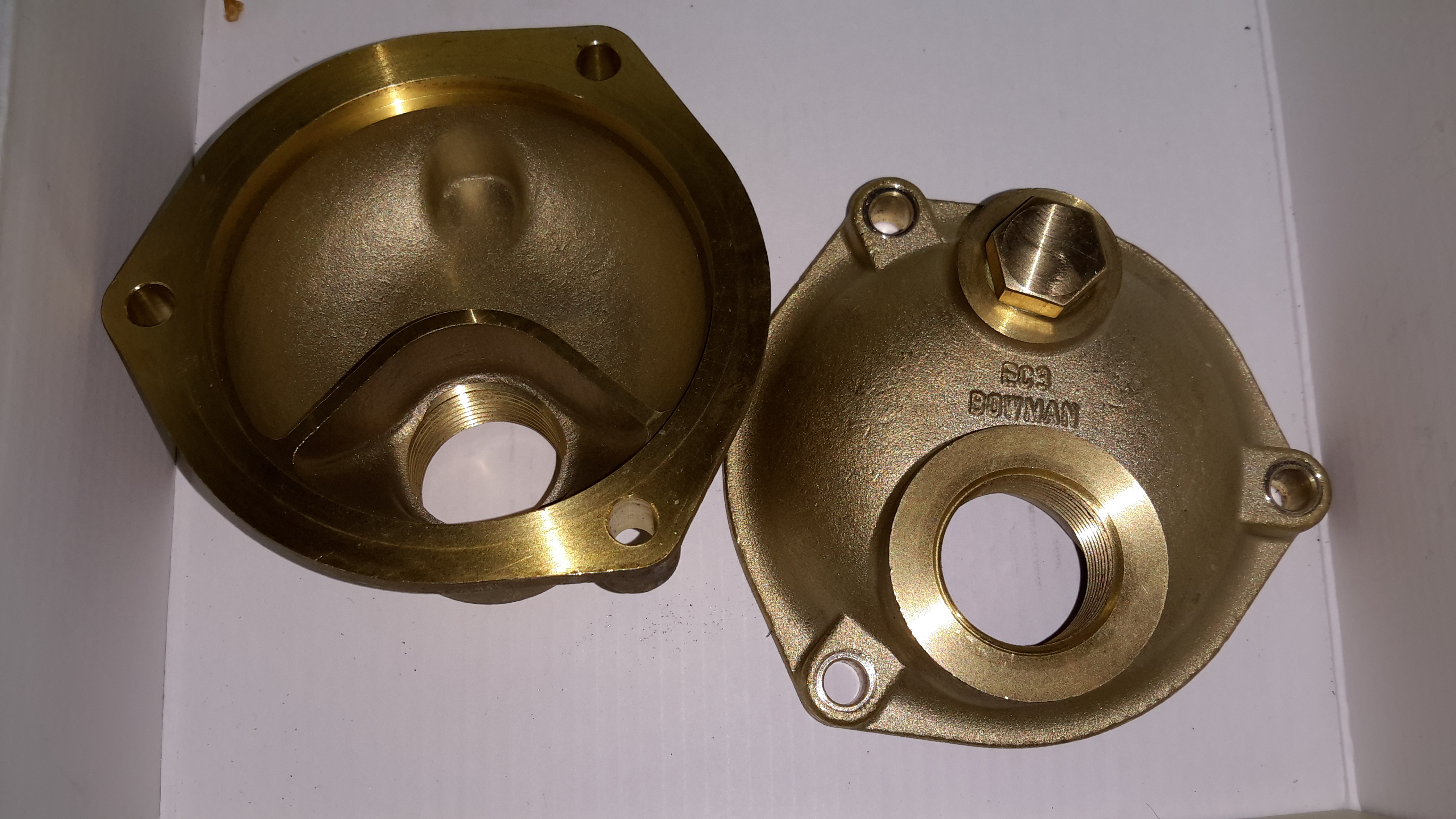
End Caps
The end caps have baffles cast in to direct the cooling water in a serpentine path, so the oil gets the best chance at dissipating it’s heat to the water.
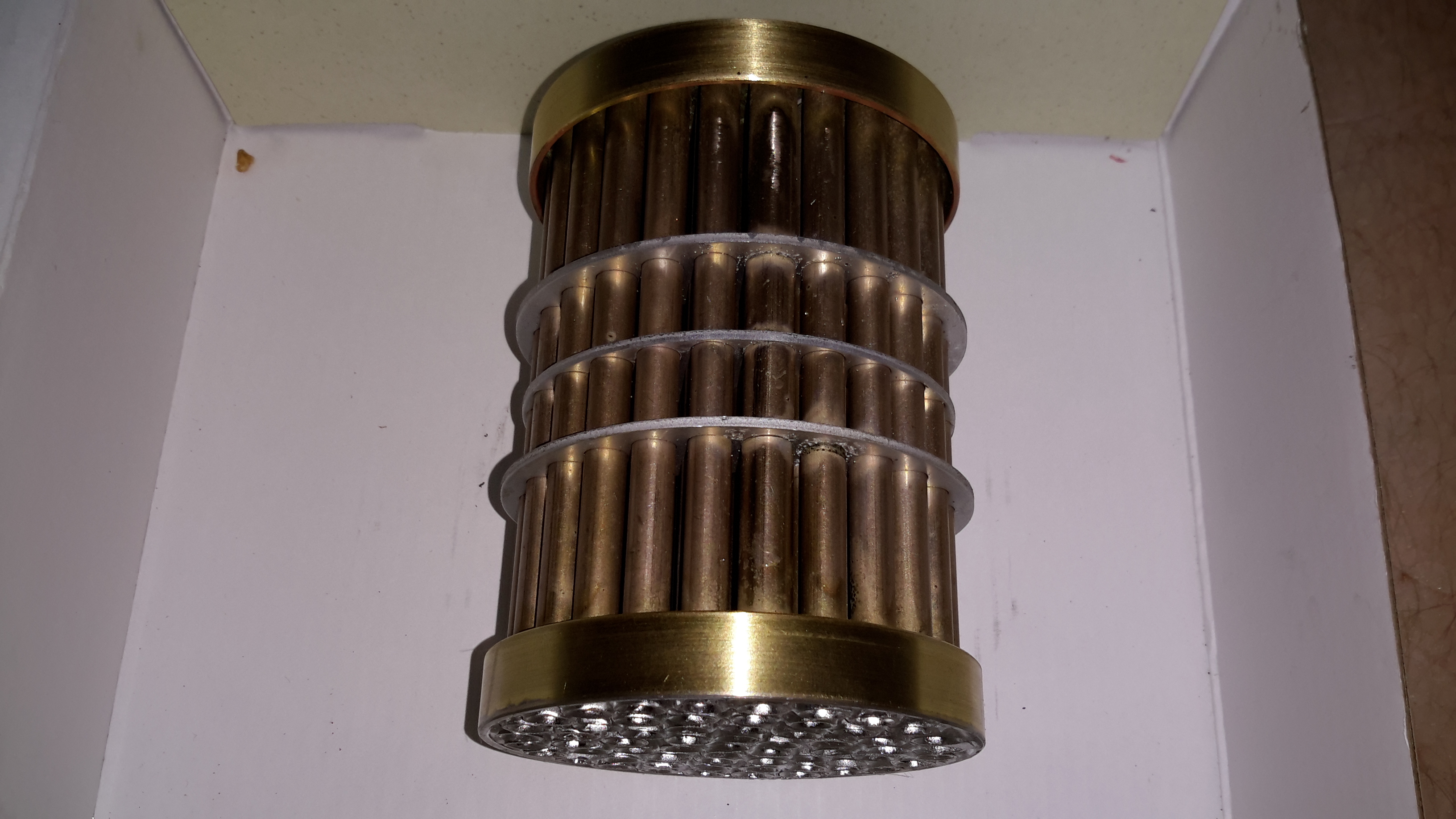
Tube Stack
The oil side of the system is on the outside of the tubes, again baffles placed along the stack direct the oil over the highest surface area possible.
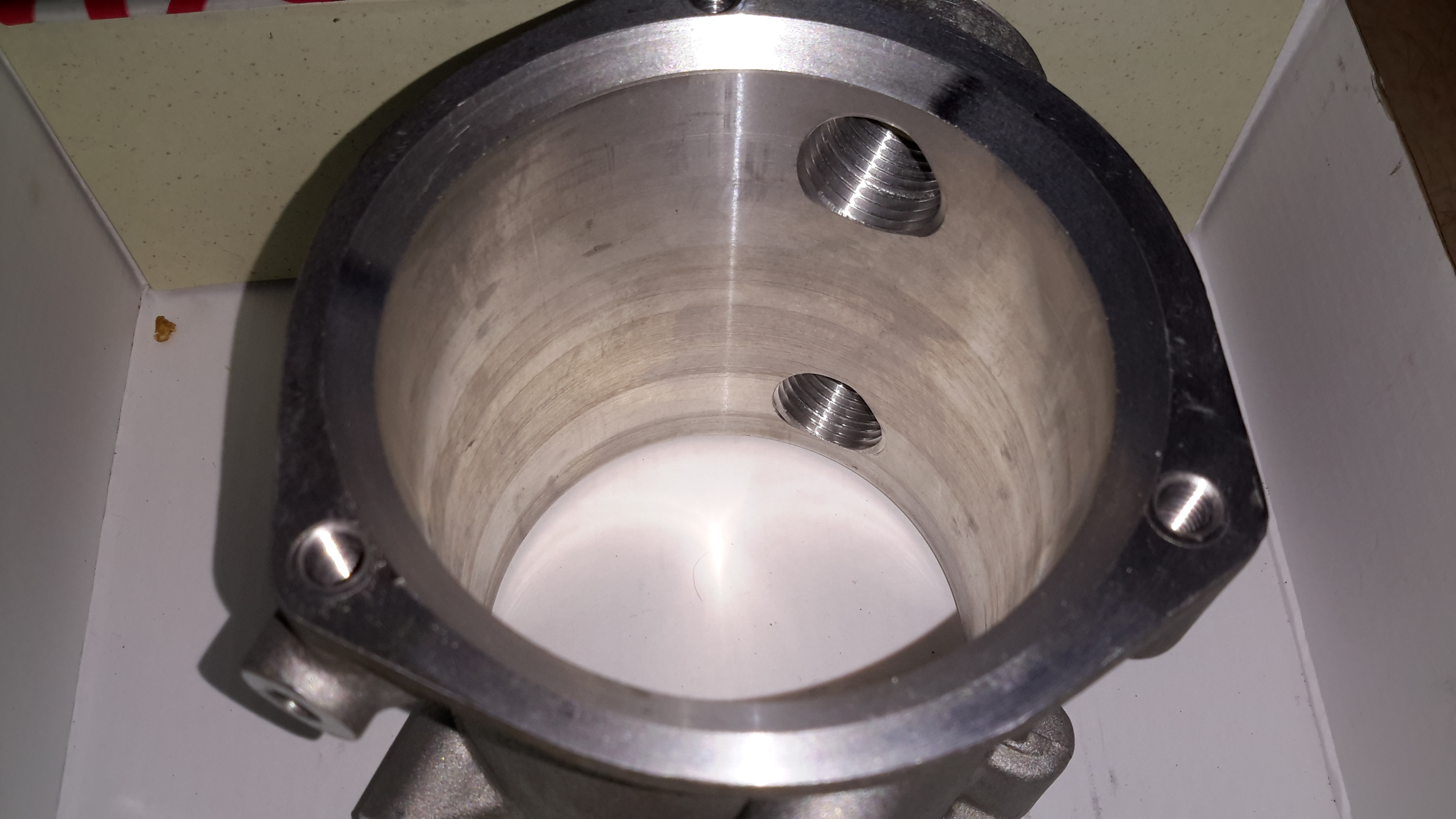
Outer Shell
The outer shell is just a machined alloy casting, with no internal features.
Magnetic tape is the medium of choice for my offline backups & archives, as it’s got an amazing level of durability when in storage. (LTO Has a 30 year archival rating).
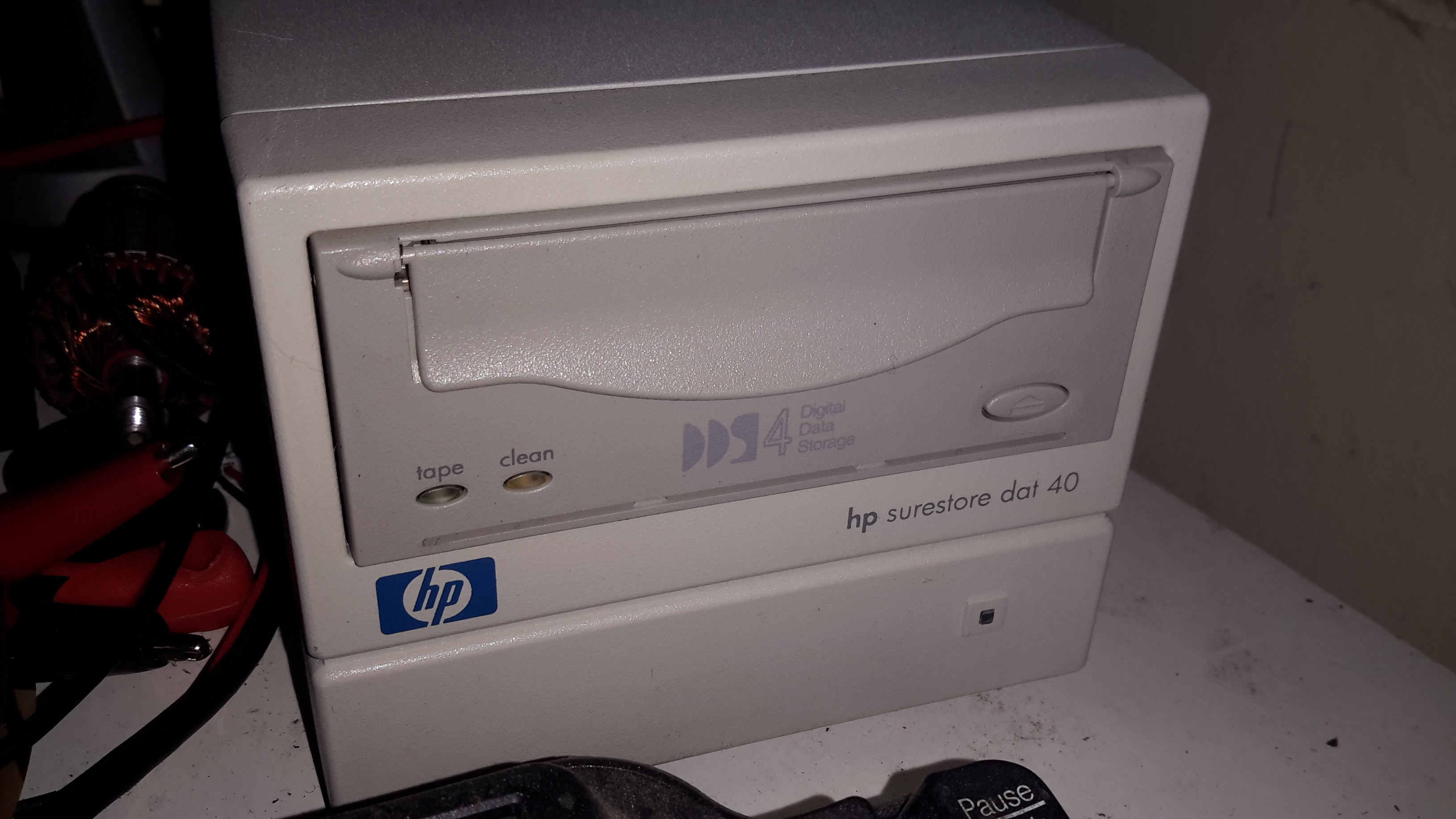
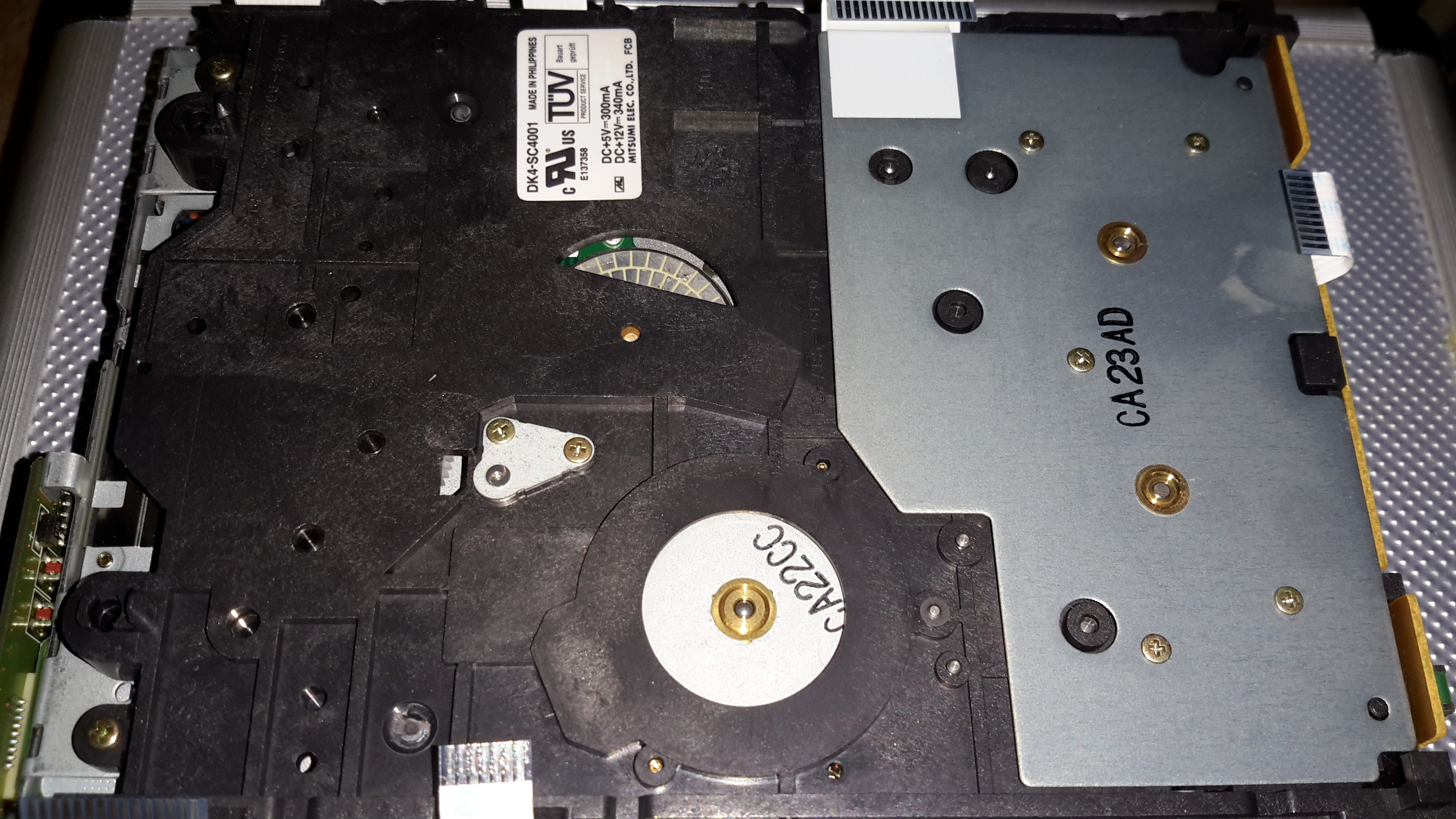
For the smaller stuff, like backing up the web server this very site runs on, another format seemed to suit better. Above is a HP DDS4 tape drive, which will store up to 40GB on a cassette compressed.
I picked this format since I already had some tapes, so it made sense.
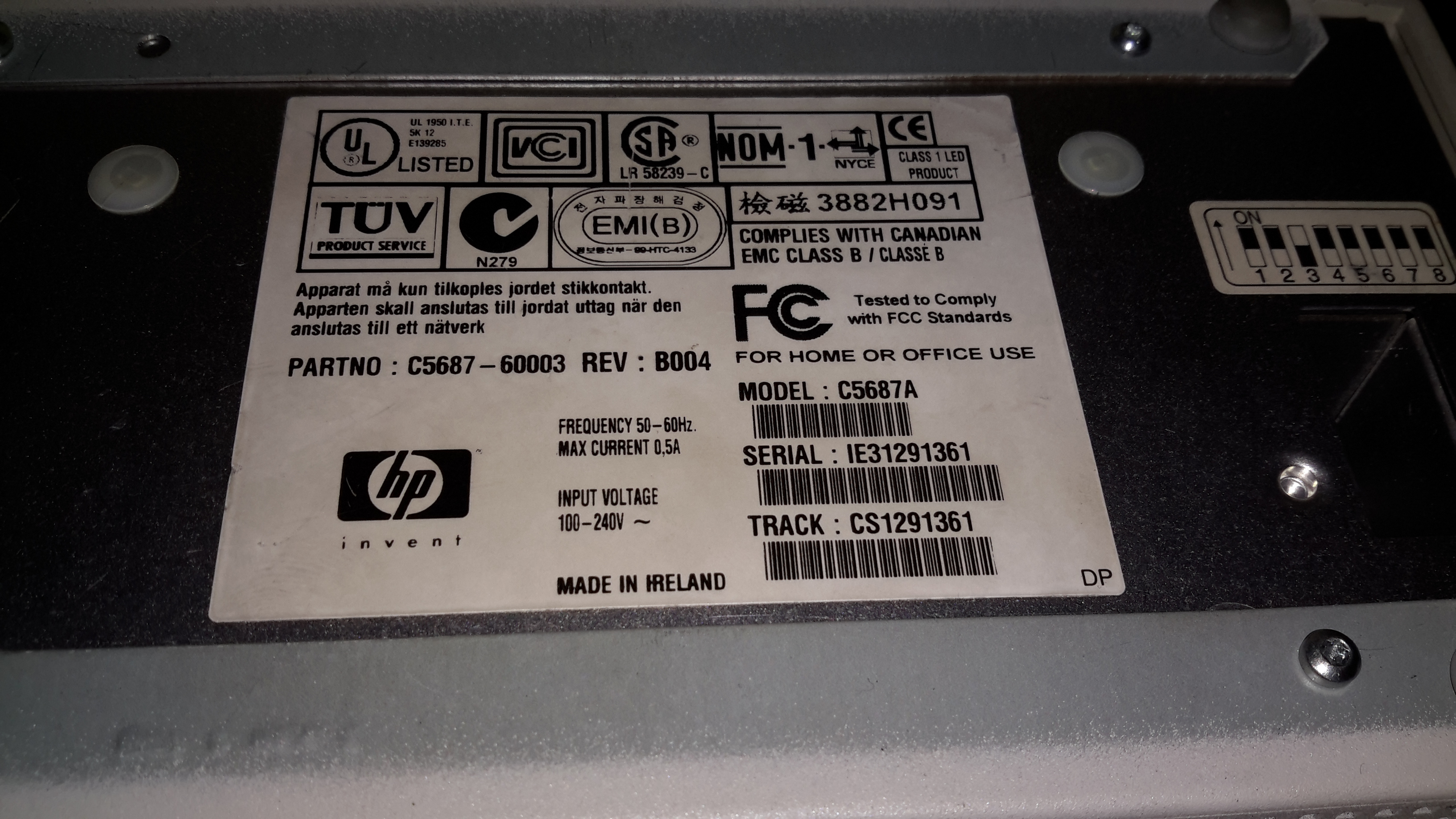
Data Plate
Here’s the info for those who want to know. It’s an older generation drive, mainly since the current generation of tape backup drives are hideously expensive, while the older ones are cheap & plentiful. Unfortunately the older generation of drives are all parallel SCSI, which can be a expensive & awkward to set up. Luckily I already have other parallel SCSI devices, so the support infrastructure for this drive was already in place.
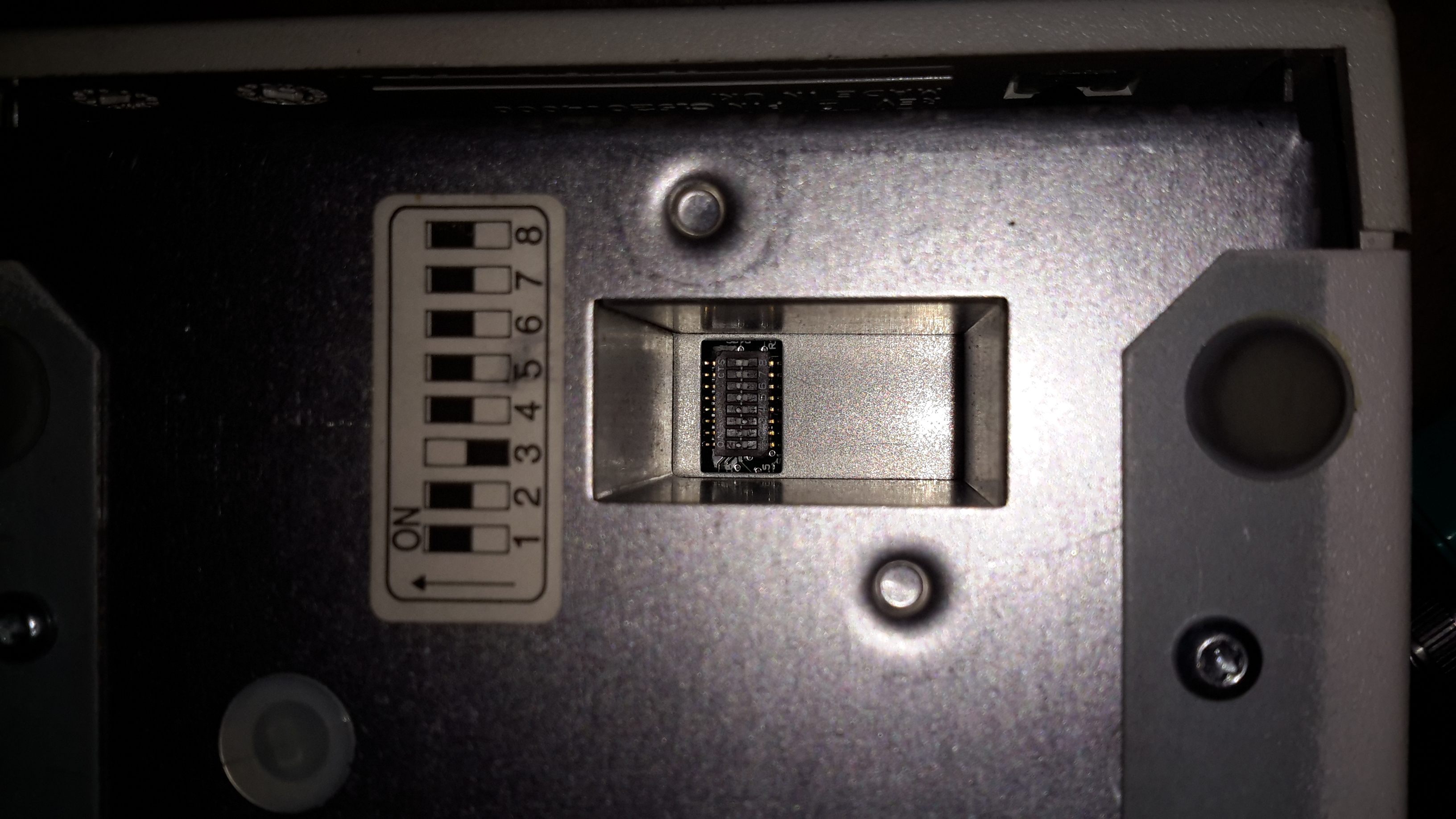
Option Switches
On the bottom of the drive is a bank of DIP switches, according to the manual these are for setting the drive for various flavours of UNIX operating systems. However it doesn’t go into what they actually change.
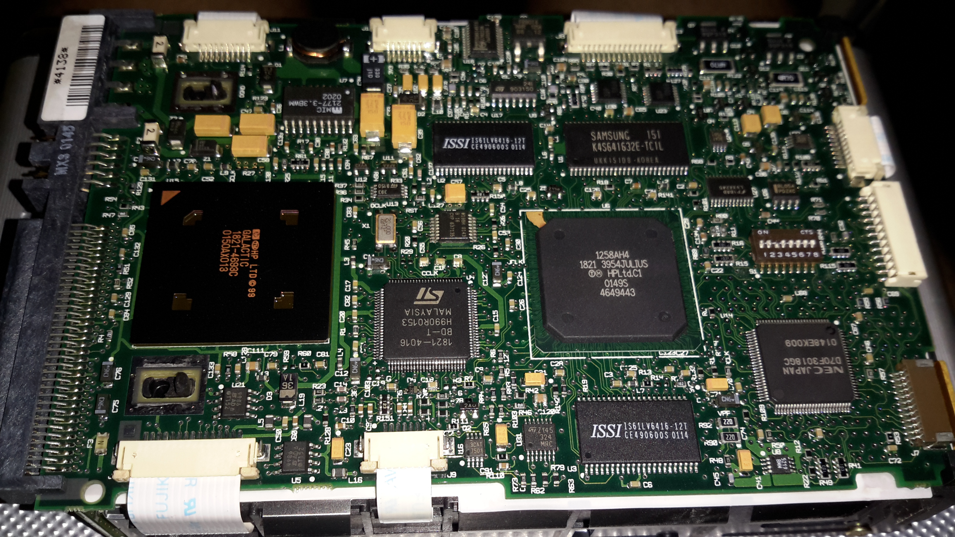
Controller PCB
The bottom of the drive has the control PCB. The large IC on the left is the SCSI interface, I’ve seen this exact same chip on other SCSI tape drives. Centre is a SoC, like so many of these, not much information available.
Drive Frame
Removing the board doesn’t reveal much else, just the bottom of the frame with the tape spool motors on the right, capstan motor bottom centre. The bottom of the head drum motor is just peeping through the plastic top centre.
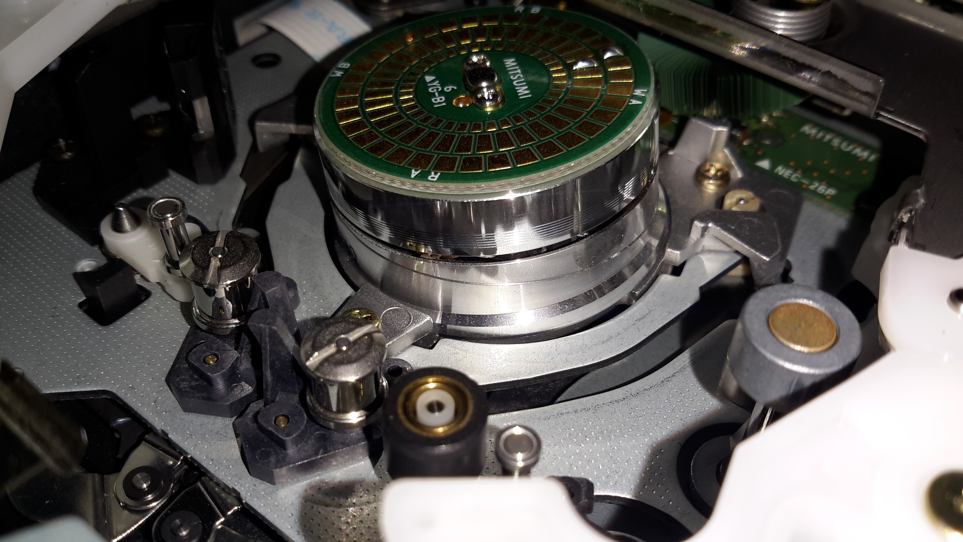
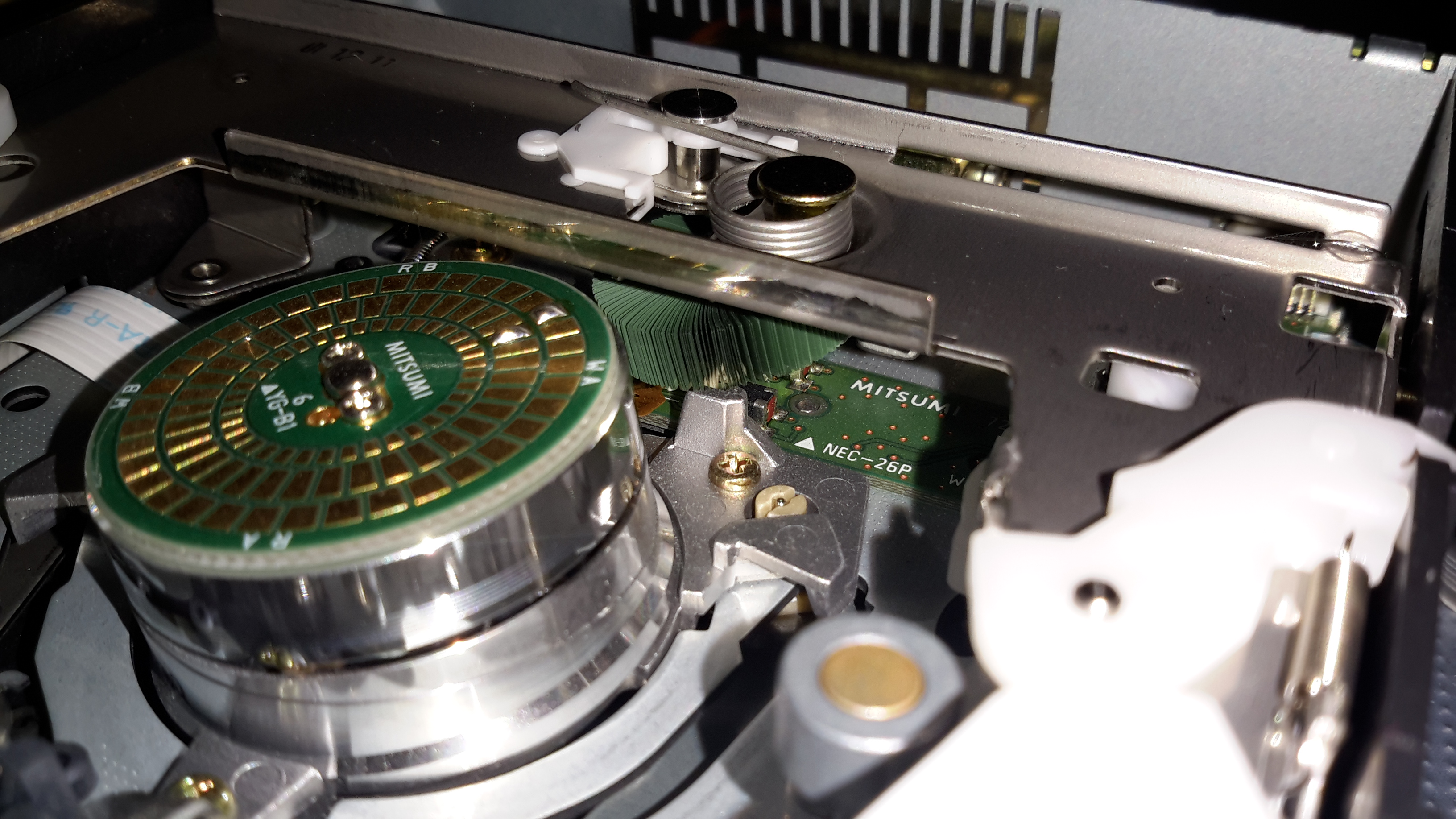
Head Drum
Here’s the head drum itself. These drives use a helical-scan flying head system, like old VHS tape decks. The top of the capstan motor is on the bottom right.
Cleaning Brush
Hidden just under the tape transport frame is the head cleaning brush. I’m not sure exactly what this is made of, but it seems to be plastic.
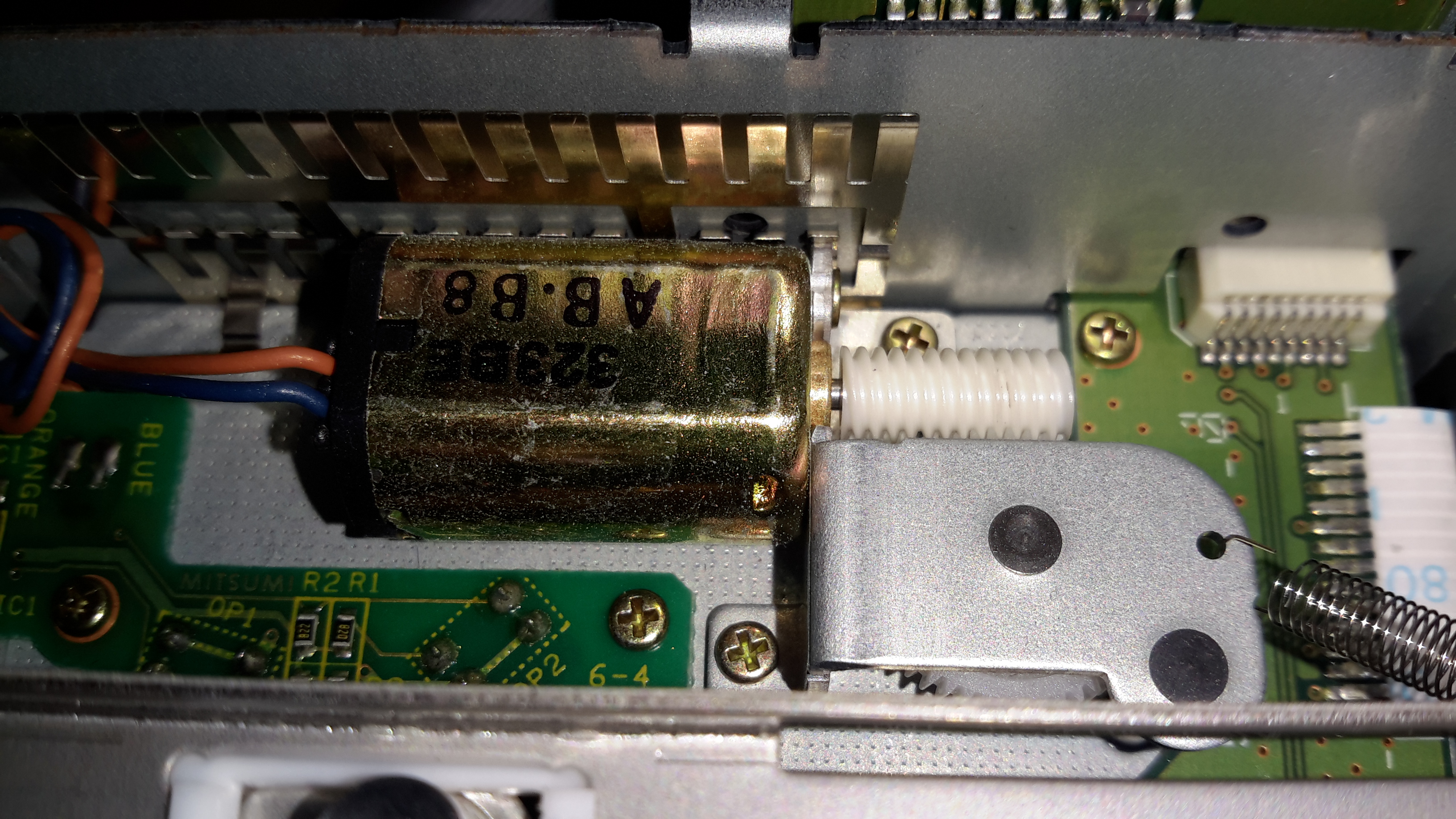
Loading Motor
A single small DC motor with a worm drive handles all tape loading tasks. The PCB to the bottom left of the motor holds several break-beam sensors that tell the drive what position the transport is in.
Tape Transport Mech
Here’s the overall tape transport. The PCB on top of the head drum is a novel idea: it’s sole purpose in life is to act as a substrate for solder blobs, used for balancing. As this drum spins at 11,400RPM when a DDS4 tape is in the drive, any slight imbalance would cause destructive vibration.
Tape Transport
Here’s the drive active & writing a tape. (A daily backup of this web server actually). The green head cleaning brush can be better seen here. The drive constantly reads back what it writes to the tape, and if it detects an error, applies this brush momentarily to the drum to clean any shed oxide off the heads. The tape itself is threaded over all the guides, around the drum, then through the capstan & pinch roller.
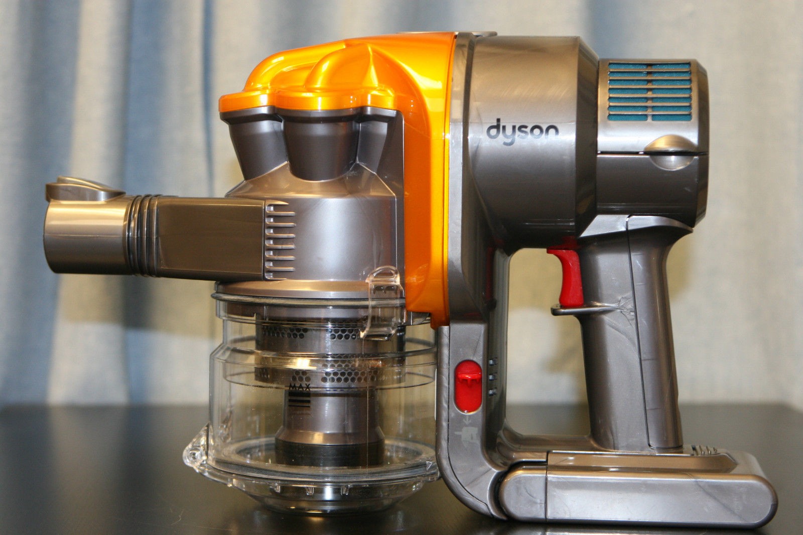
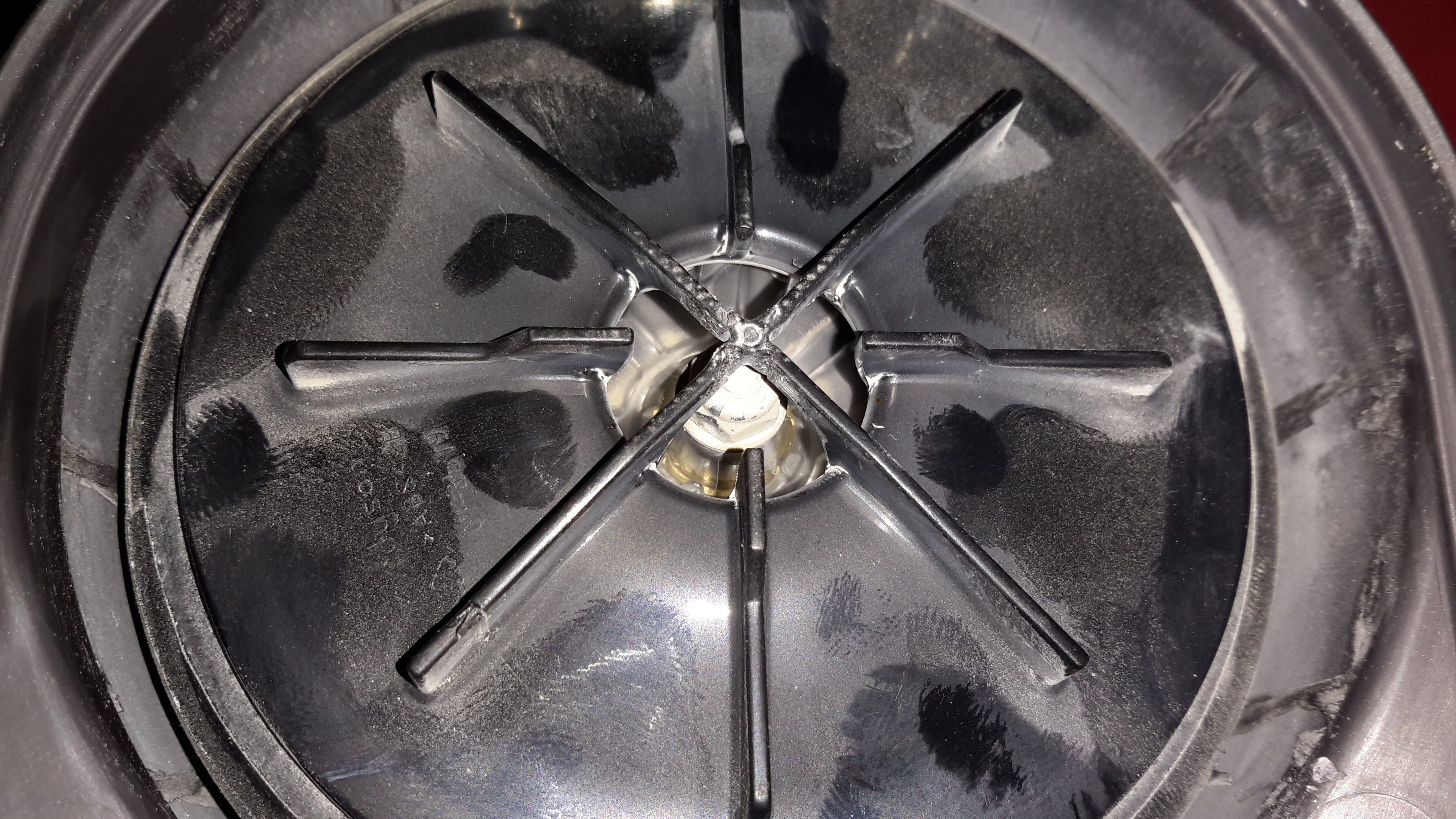
The Dyson DC16 is one of the older handheld vacuums, before the introduction of the “Digital Motor”. (Marketing obviously didn’t think “Switched Reluctance Motor” sounded quite as good).
These vacuums have a very large DC brush motor driving the suction turbine instead, the same as would be found in a cordless power tool.
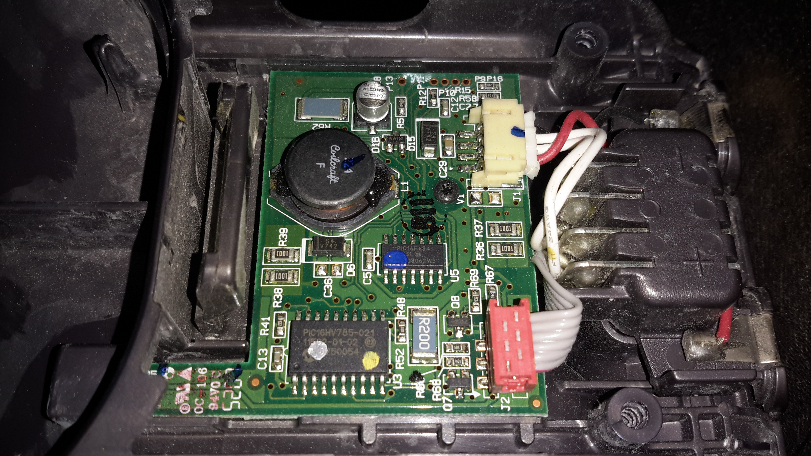
Control PCB
Popping the front cap off with the ID label, reveals the brains of the vacuum. The two large terminals at the right are for charging, which is only done at 550mA (0.5C). There are two PIC microcontrollers in here, along with a large choke, DC-DC converter for supplying the logic most likely. The larger of the MCUs, a PIC16HV785, is probably doing the soft-start PWM on the main motor, the smaller of the two, a PIC16F684 I’m sure is doing battery charging & power management. The motor has a PCB on it’s tail end, with a very large MOSFET, a pair of heavy leads connect directly from the battery connector to the motor.
Just out of sight on the bottom left edge of the board is a Hall Effect Sensor, this detects the presence of the filter by means of a small magnet, the vacuum will not start without a filter fitted.
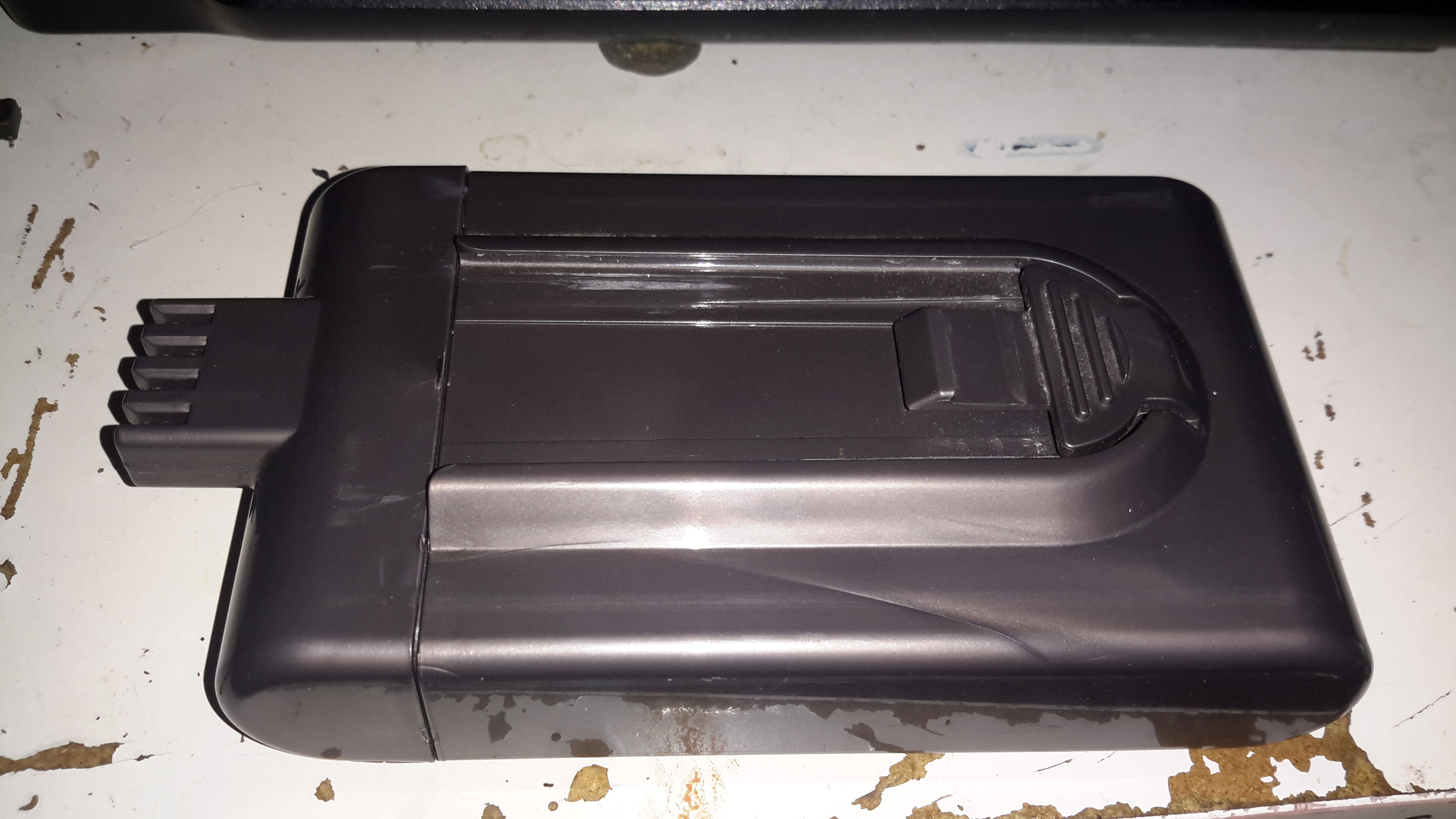
Battery Pack
The battery pack is a large custom job, obviously. 4 terminals mean there’s slightly more in here than just the cells.
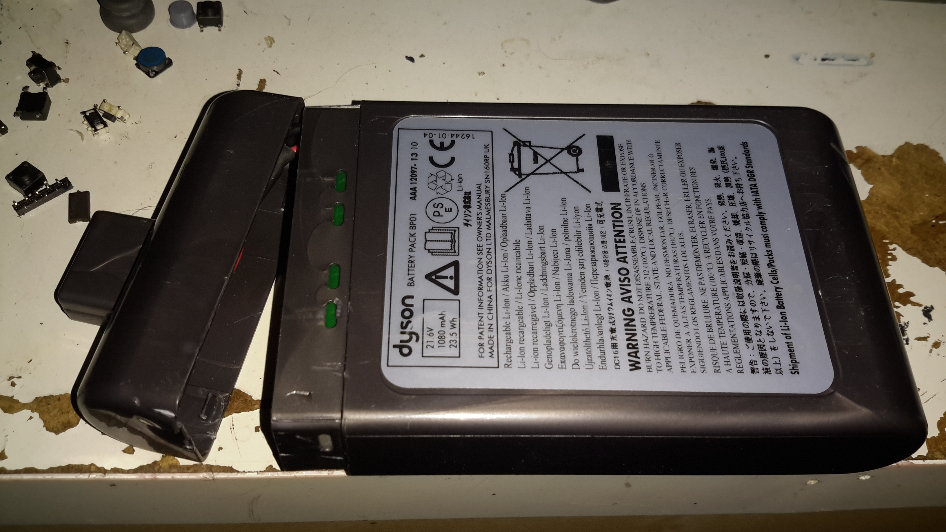
Battery Cracked
Luckily, instead of ultrasonic or solvent welding the case, these Dyson batteries are just snapped together. Some mild attack with a pair of screwdrivers allows the end cap to be removed with minimal damage.
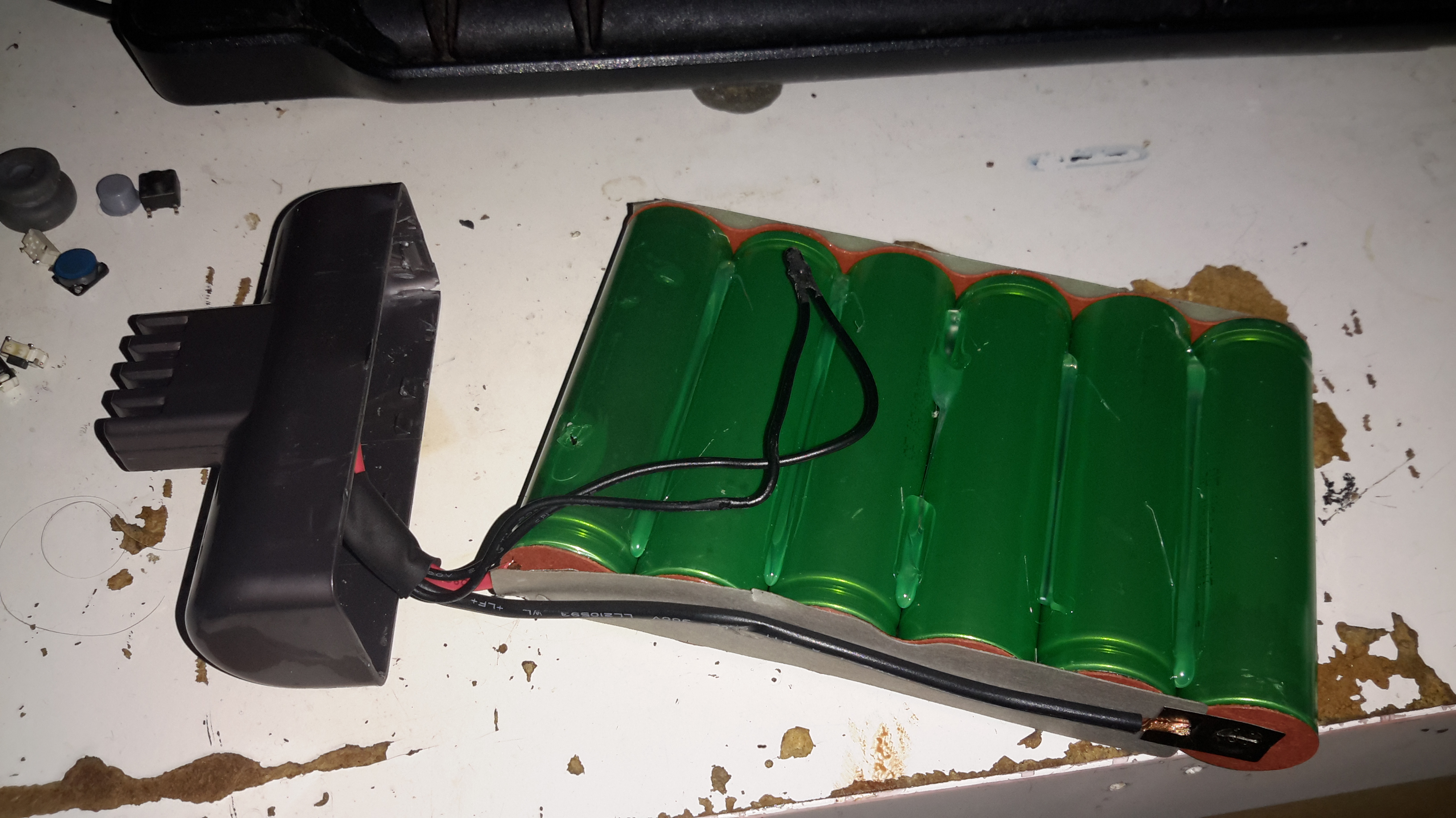
Cells
The cells were lightly hot-glued into the shell, but that can easily be solved with a drop of Isopropanol to dissolve the glue bond. The pack itself is made up of 6 Sony US18650VT High-Drain 18650 Li-Ion cells in series for 21.6v nominal. These are rated at a max of 20A discharge current, 10A charge current, and 1.3Ah capacity nominal.
There’s no intelligence in this battery pack, the extra pair of terminals are for a thermistor, so the PIC in the main body knows what temperature the pack is at – it certainly gets warm while in use due to the high current draw.
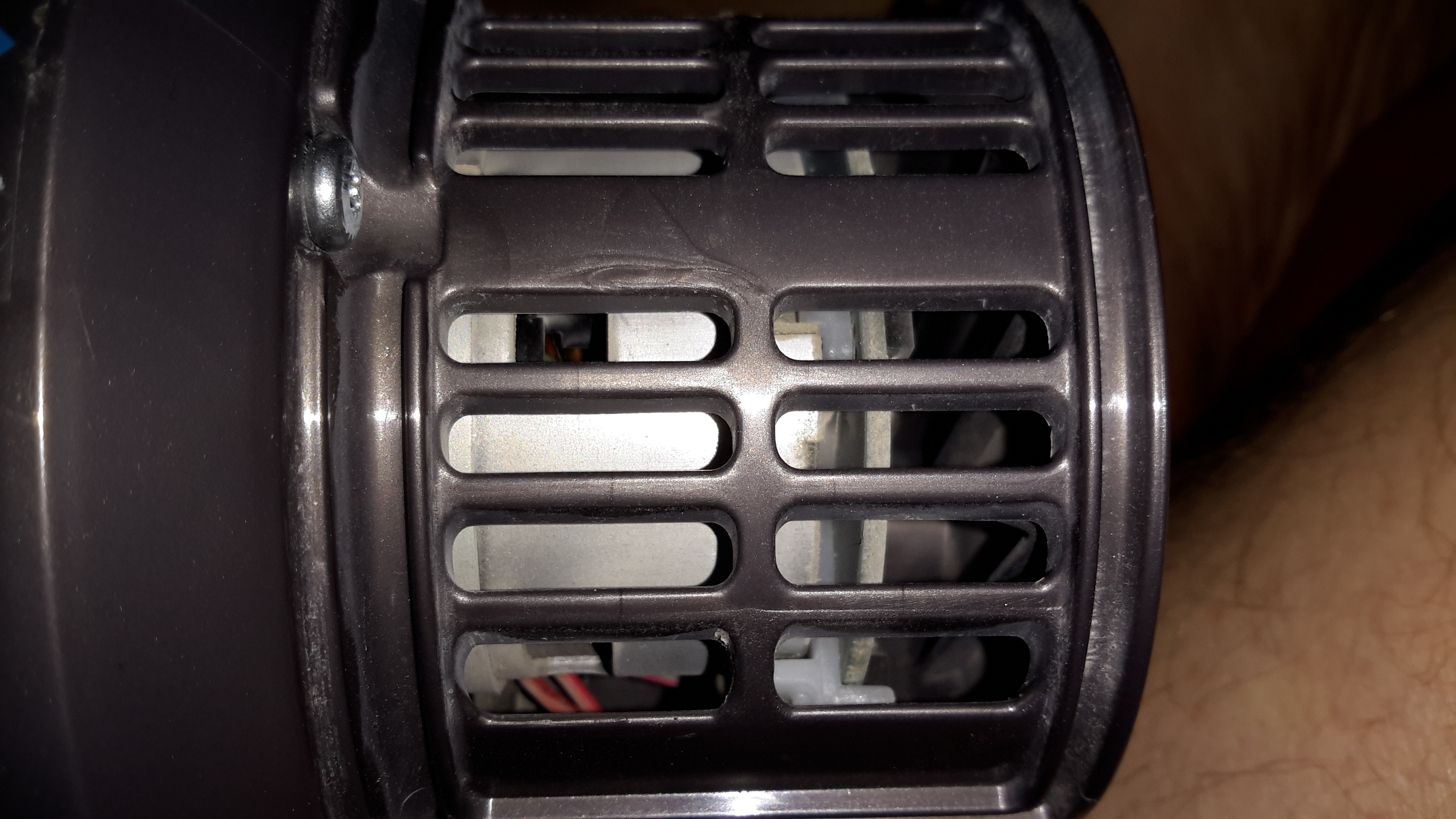
Motor
Hidden in the back side of the main body is the motor. Unfortunately I wasn’t able to get this out without doing some damage, as the wiring isn’t long enough to free the unit without some surgery.
Turbine
The suction is generated by a smaller version of the centrifugal high-speed blowers used in full size vacuums. Not much to see here.
Unofficial Charger
Since I got this without a charger, I had to improvise. The factory power supply is just a 28v power brick, all the charging logic is in the vacuum itself, so I didn’t have to worry about such nasties as over-charging. I have since fitted the battery pack with a standard Li-Po balance cable, so it can be used with my ProCell charger, which will charge the pack in 35 minutes, instead of the 3 hours of the original charger.
I recently came across these on eBay, so I thought I’d grab one to see how they function, with all the metrics they display, there’s potential here for them to be very useful indeed.
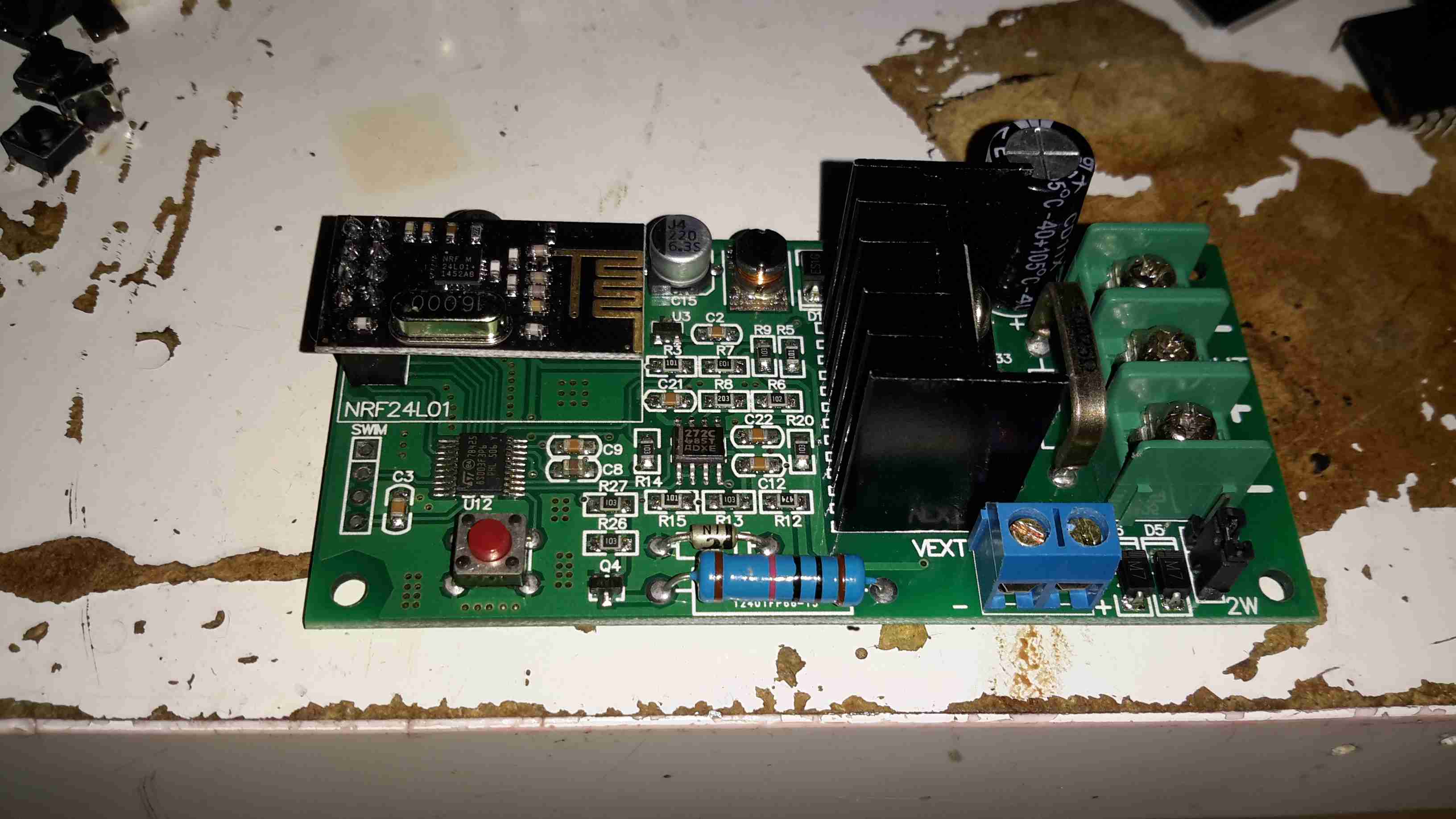
One of the best parts is that no wiring is required between the sensor board & the LCD head unit – everything is transmitted over a 2.4GHz data link using NRF24L01 modules.
Above is the display unit, with it’s colour LCD display. Many features are available on this, & they appear to be designed for battery powered systems.
Monitor PCB
Another PCB handles the current & voltage sensing, so this one can be mounted as close to the high current wiring as possible.
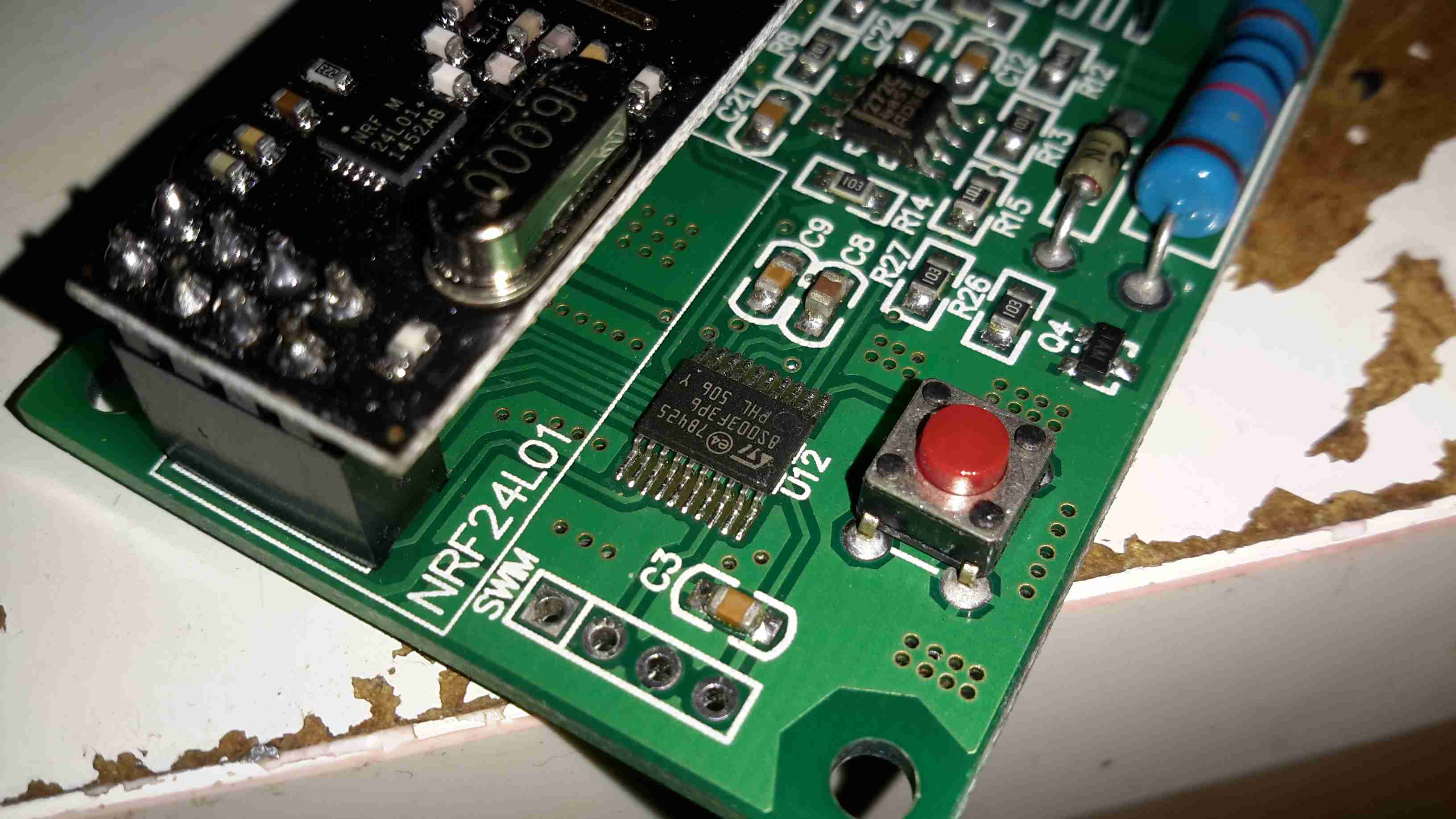
Monitor PCB Microcontroller
The transmitter PCB is controlled with an STM8S003F3 microcontroller from ST Microelectronics. This is a Flash based STM with 8KB of ROM, 1KB of RAM & 10-bit ADC. The NRF24L01 transceiver module is just to the left.
There’s only a single button on this board, for pairing both ends of the link.
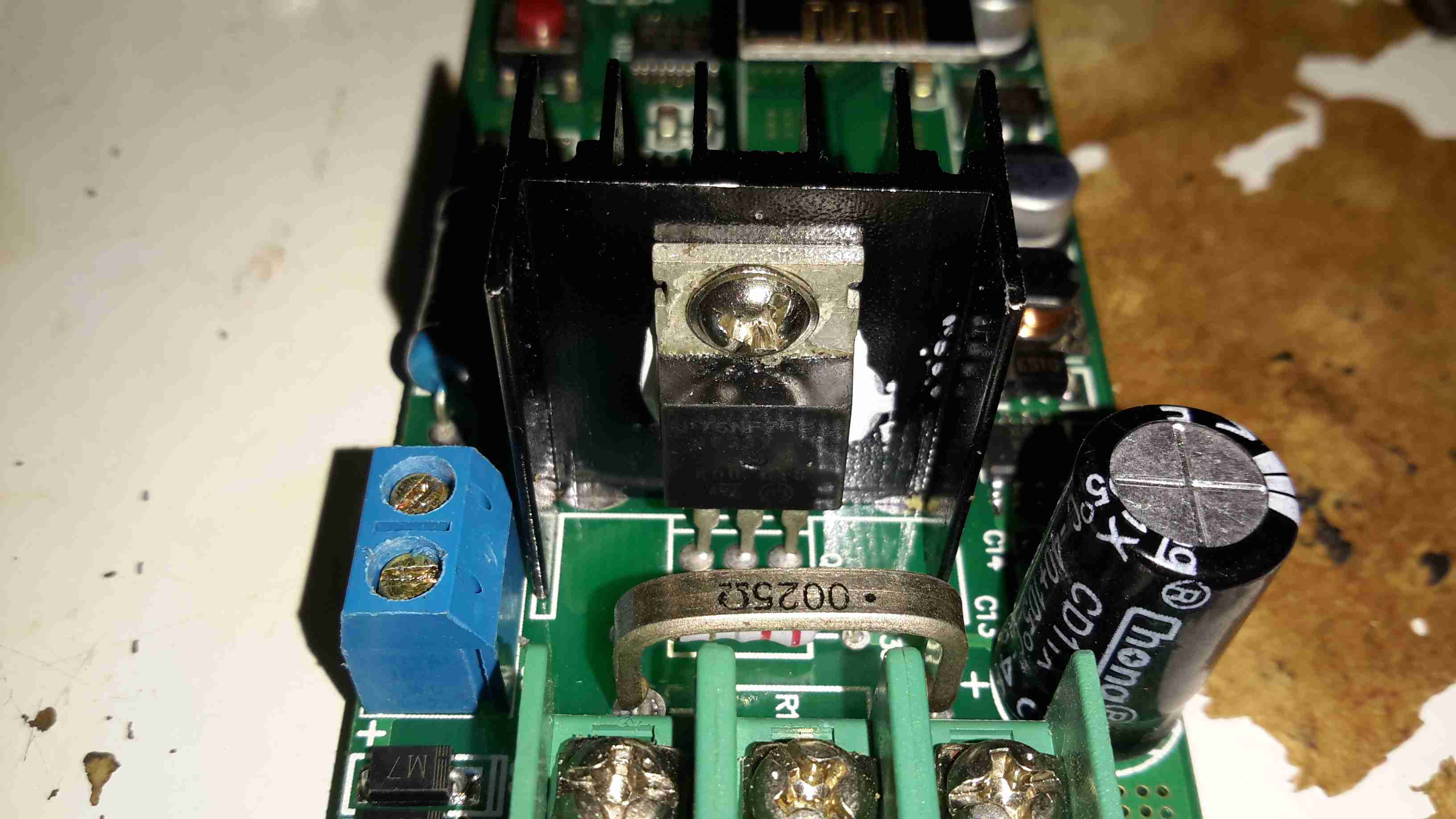
Output MOSFET
The high current end of the board has the 0.0025Ω current shunt & the output switch MOSFET, a STP75NF75 75v 75A FET, also from ST Microelectronics. A separate power source can be provided for the logic via the blue terminal block instead of powering from the source being measured.
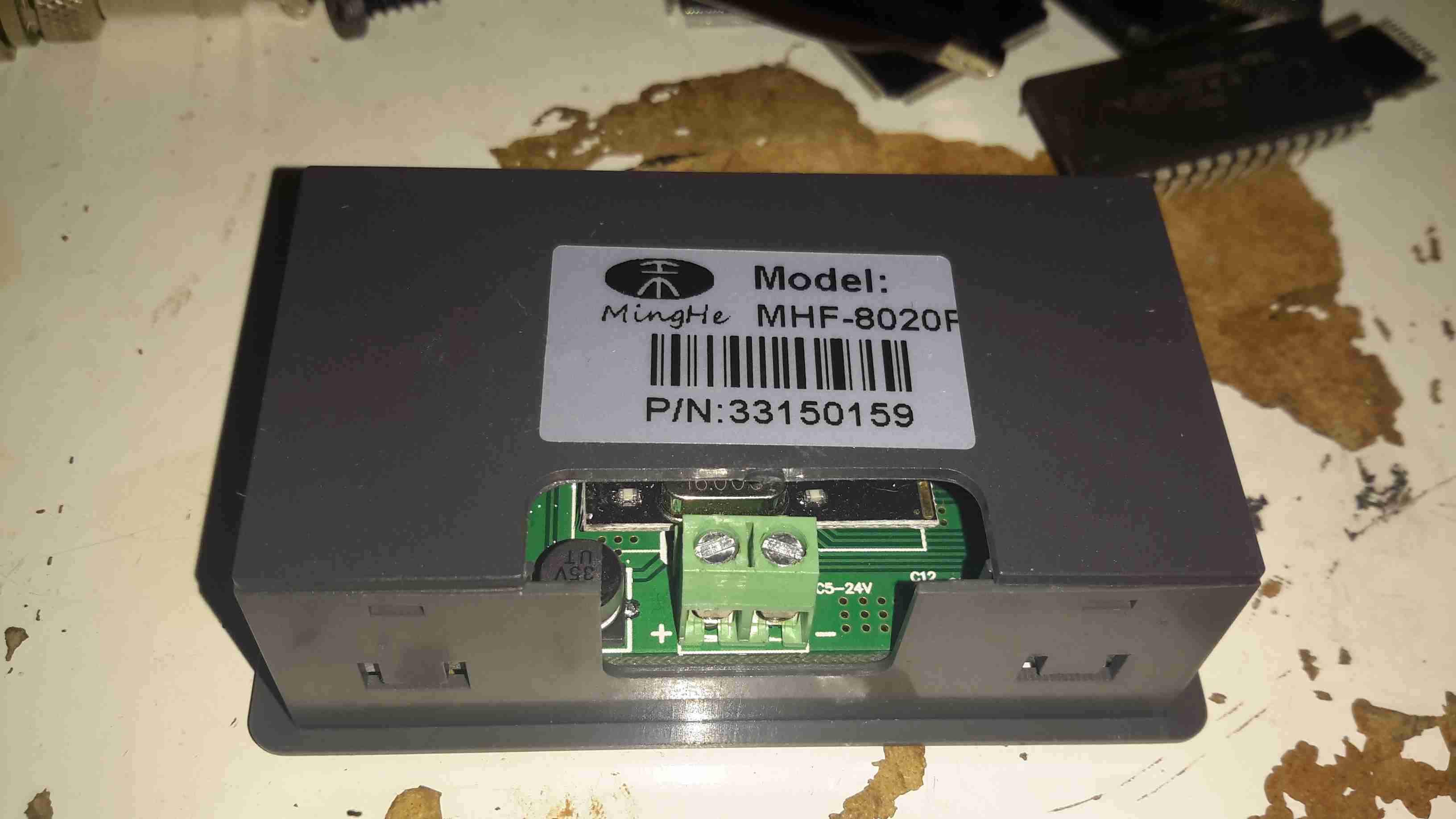
LCD Unit Rear
Here’s the display unit, only a pair of power terminals are provided, 5-24v wide-range input is catered for.
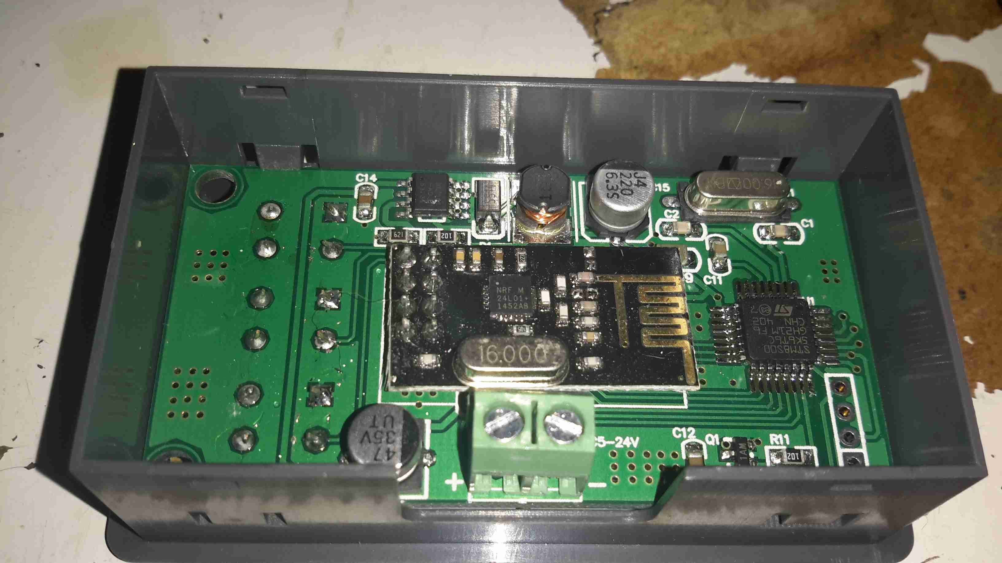
LCD Unit PCB
Unclipping the back of the board reveals the PCB, with another 2.4GHz NRF24L01 module, and a STM8S005K6 microcontroller in this case. The switching power supply that handles the wide input voltage is along the top edge of the board.
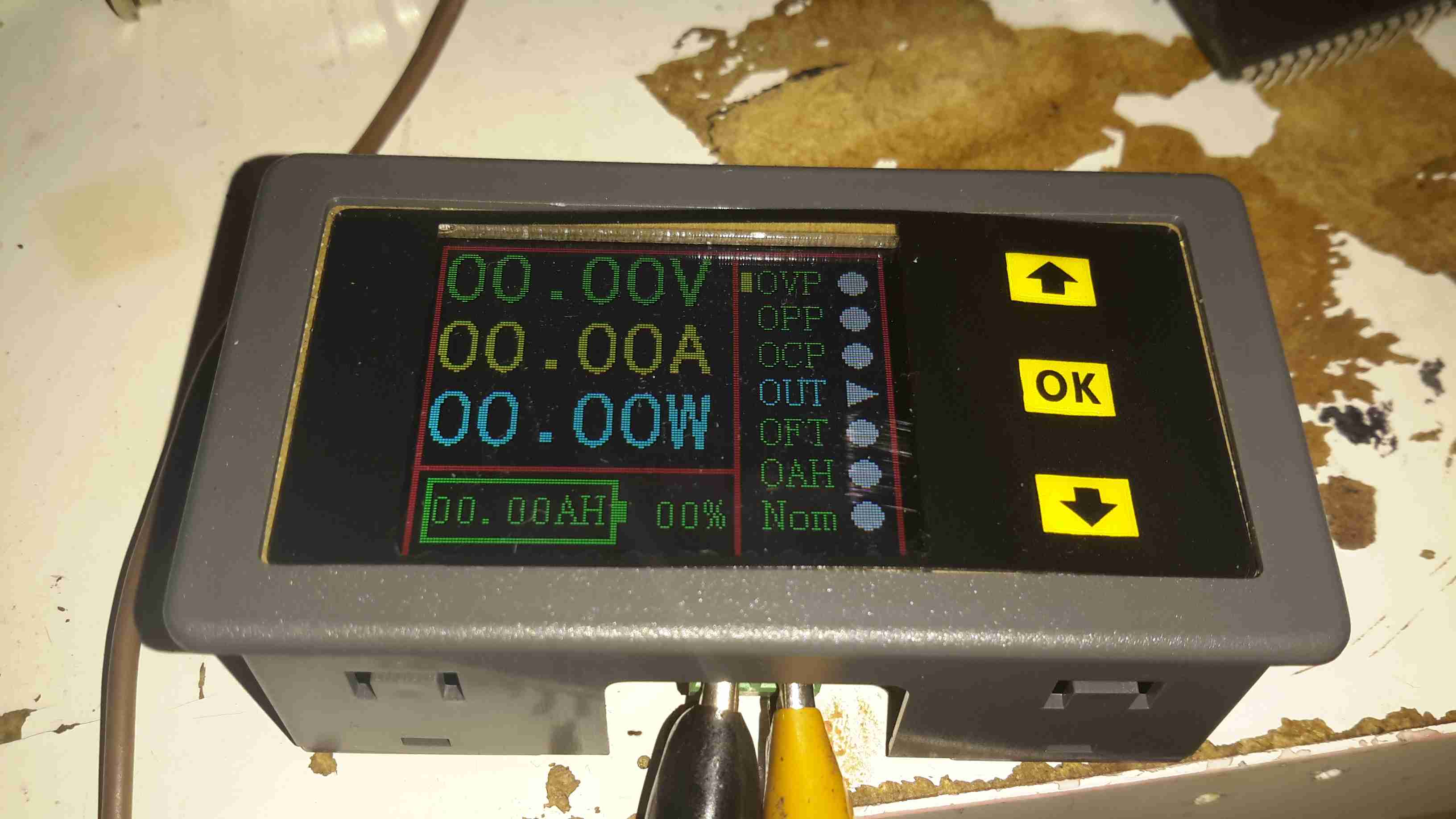
Unfortunately I didn’t get any instruction manual with this, so some guesswork & translation of the finest Chinglish was required to get my head round the way everything works. To make life a little easier for others that might have this issue, here’s a list of functions & how to make them work.
LCD Closeup
On the right edge of the board is the function list, a quick press of the OK button turns a function ON/OFF, while holding it allows the threshold to be set.
When the output is disabled by one of the protection functions, turning that function OFF will immediately enable the output again.
The UP/DOWN buttons obviously function to select the desired function with the cursor just to the left of the labels. Less obviously though, pressing the UP button while the very top function is selected will change the Amp-Hours display to a battery capacity icon, while pressing DOWN while the very bottom function is selected will change the Watts display to Hours.
The round circle to the right displays the status of a function. Green for OK/ON Grey for FAULT/OFF.
OVP: Over voltage protection. This will turn off the load when the measured voltage exceeds the set threshold.
OPP: Over power protection. This function prevents a load from pulling more than a specified number of watts from the supply.
OCP: Over current protection. This one’s a little more obvious, it’ll disable the output when the current measured exceeds the specified limit.
OUT: This one is the status of the output MOSFET. Can also be used to manually enable/disable the output.
OFT: Over time protection. This one could be useful when charging batteries, if the output is enabled for longer than the specified time, the output will toggle off.
OAH: Over Amp-Hours protection. If the counted Amp-Hours exceeds the set limit, the output will be disabled.
Nom: This one indicates the status of the RF data link between the modules, and can be used to set the channel they operate on.
Pairing is achieved by holding the OK button, selecting the channel on the LCD unit, and then pressing the button on the transmitter board. After a few seconds, (it appears to scan through all addresses until it gets a response) the display will resume updating.
This function would be required if there are more than a single meter within RF range of each other.
I’ve not yet had a proper play with all the protection functions, but a quick mess with the OVP setting proved it was very over-sensitive. Setting the protection voltage to 15v triggered the protection with the measured voltage between 12.5v-13.8v. More experimentation is required here I think, but as I plan to just use these for power monitoring, I’ll most likely leave all the advanced functions disabled.
This camera has now been retired after many years of heavy use. Exposure to a 3-year old has caused severe damage to the lens mechanism, which no longer functions correctly.
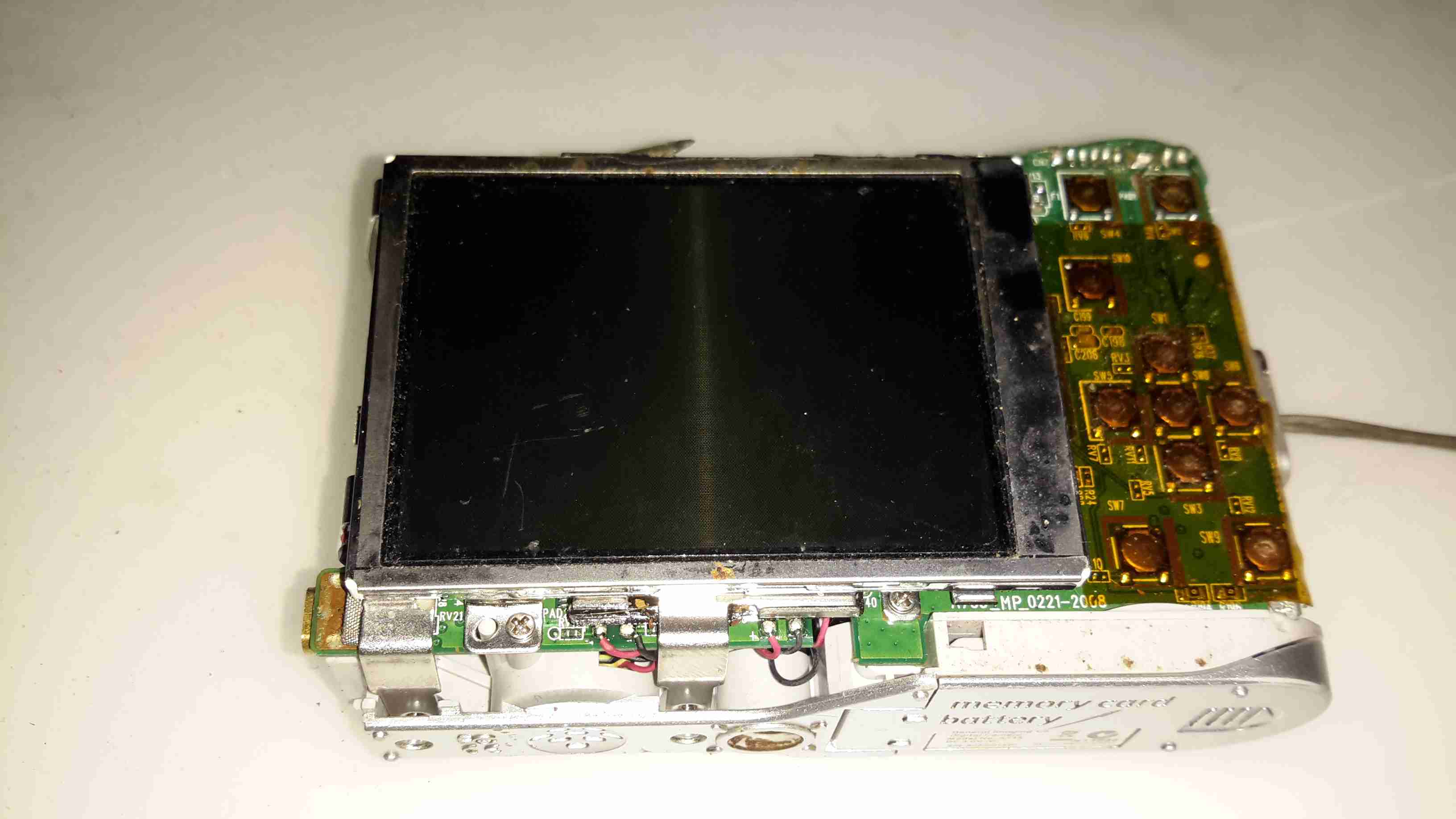
Rear Panel
Pretty much standard interface for a digital camera, with a nice large LCD for it’s time.
Front Cover Removed
With the front cover removed, the lens assembly & battery compartment is exposed.
Rear Cover Removed
Removing the rear cover exposes the LCD module & the main PCB, the interface tactile switches are on the right under a protective layer of Kapton tape.
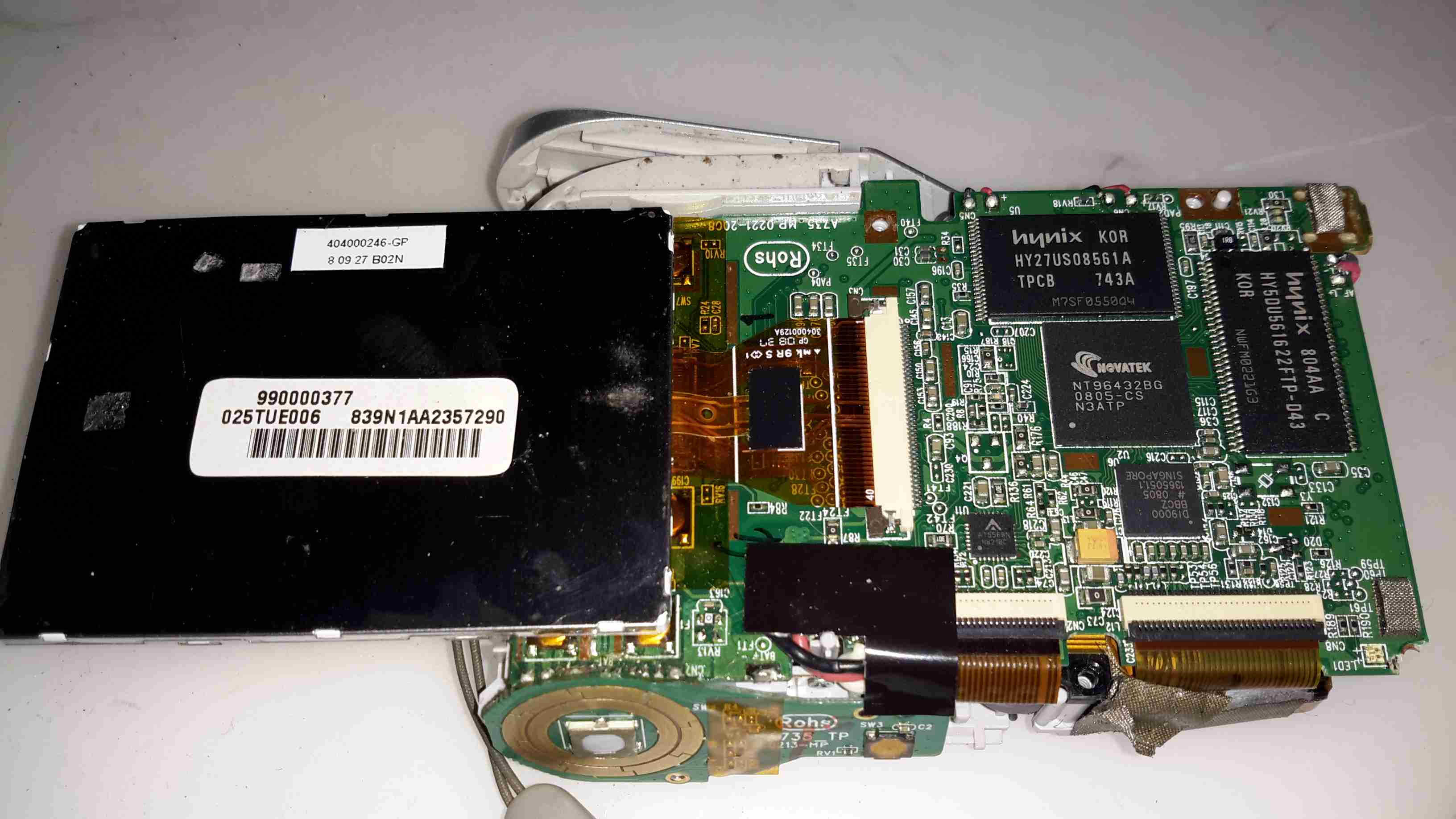
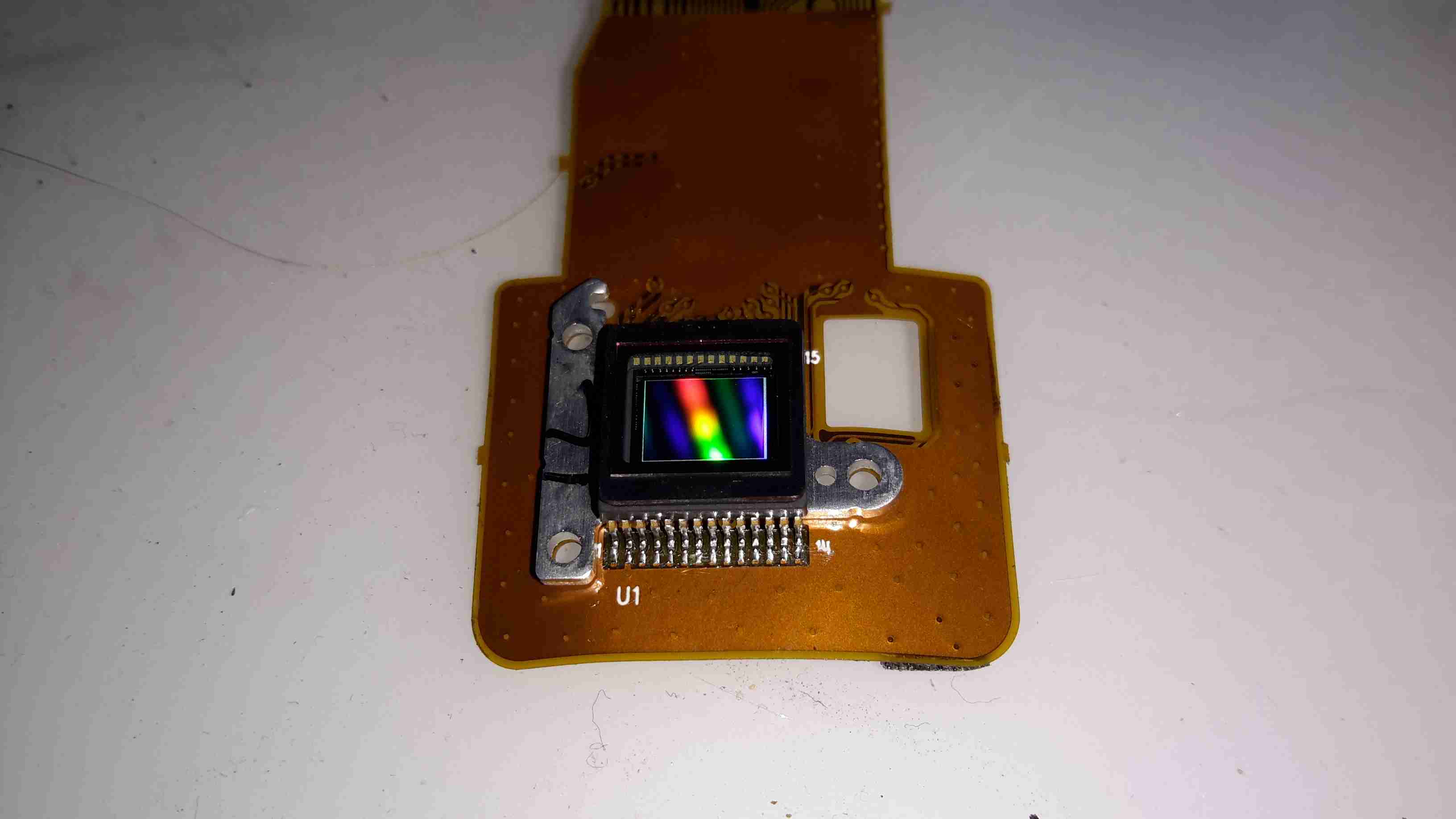
Main Chipset
Flipping the LCD out of it’s mounting bracket reveals the main camera chipset. The CPU is a NovaTek NT96432BG, no doubt a SoC of some kind, but I couldn’t find any information. Firmware & inbuilt storage is on a Hynix HY27US08561A 256MBit NAND Flash, with a Hynix HY5DU561622FTP-D43 256Mbit DRAM for system memory.
I couldn’t find any info on the other two chips on this side of the board, but one is probably a motor driver for the lens, while the other must be the front end for the CCD sensor input to the SoC.
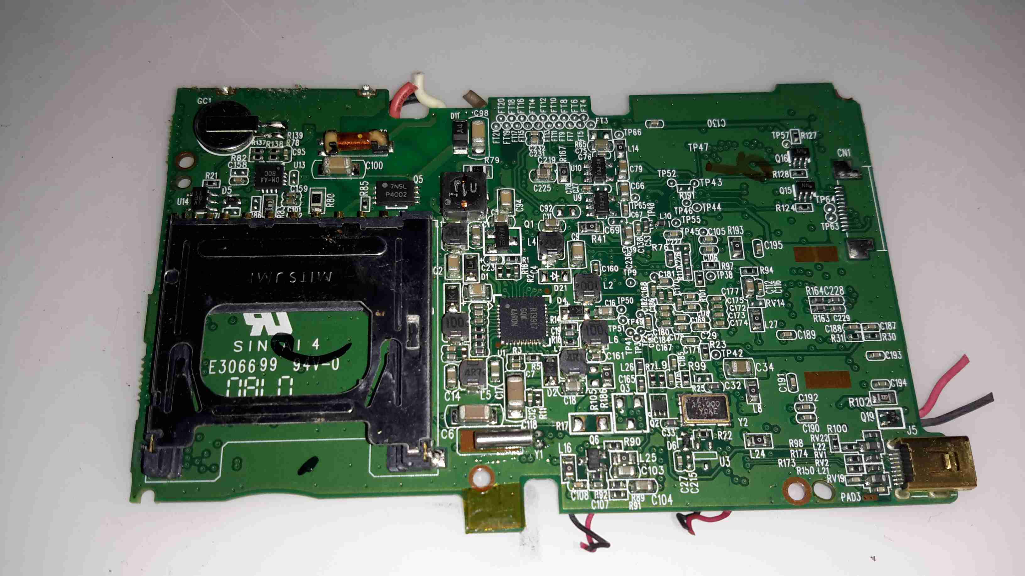
Main PCB Reverse
The other side of the PCB handles the SD card slot & power management. All the required DC rails are provided for by a RT9917 7-Channel DC-DC converter from RichTek, an IC designed specifically for digital camera applications.
Top left above the SD card slot is the trigger circuitry for the Xenon flash tube & the RTC backup battery.
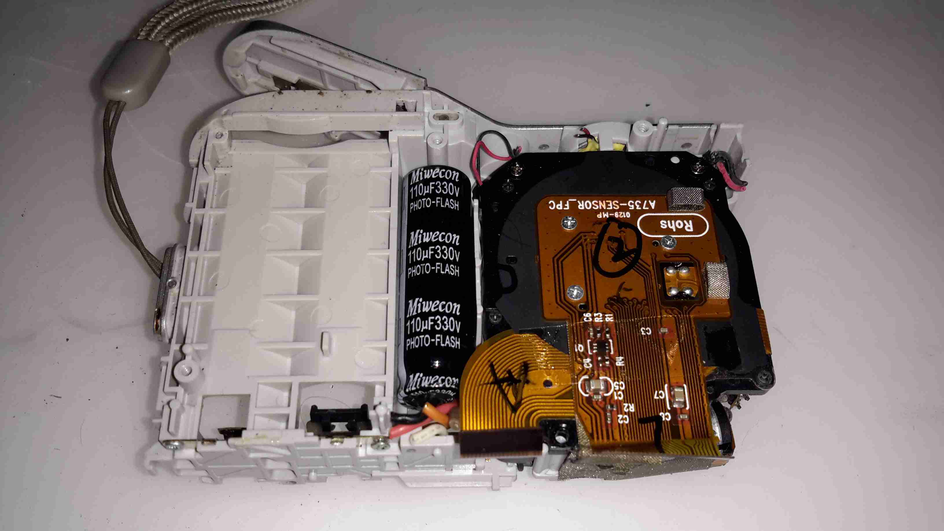
Main PCB Removed
Once the main PCB is out of the frame, the back of the lens module with the CCD is accessible. Just to the left is the high-voltage photoflash capacitor, 110µF 330v. These can give quite the kick when charged! Luckily this camera has been off long enough for the charge to bleed off.
Sensor
Finally, here’s the 7-Megapixel CCD sensor removed from the lens assembly, with it’s built in IR cut filter over the top. I couldn’t find any make or model numbers on this part, as the Aluminium mounting bracket behind is bonded to the back of the sensor with epoxy, blocking access to any part information.
Die images of the chipset to come once I get round to decapping them!
As I’ve been posting some photos of decapped ICs lately, I thought I’d share the process I use personally for those that might want to give it a go 😉
The usual method for removing the epoxy package from the silicon is to use hot, concentrated Nitric Acid. Besides the obvious risks of having hot acids around, the decomposition products of the acid, namely NO² (Nitrogen Dioxide) & NO (Nitrogen Oxide), are toxic and corrosive. So until I can get the required fume hood together to make sure I’m not going to corrode the place away, I’ll leave this process to proper labs ;).
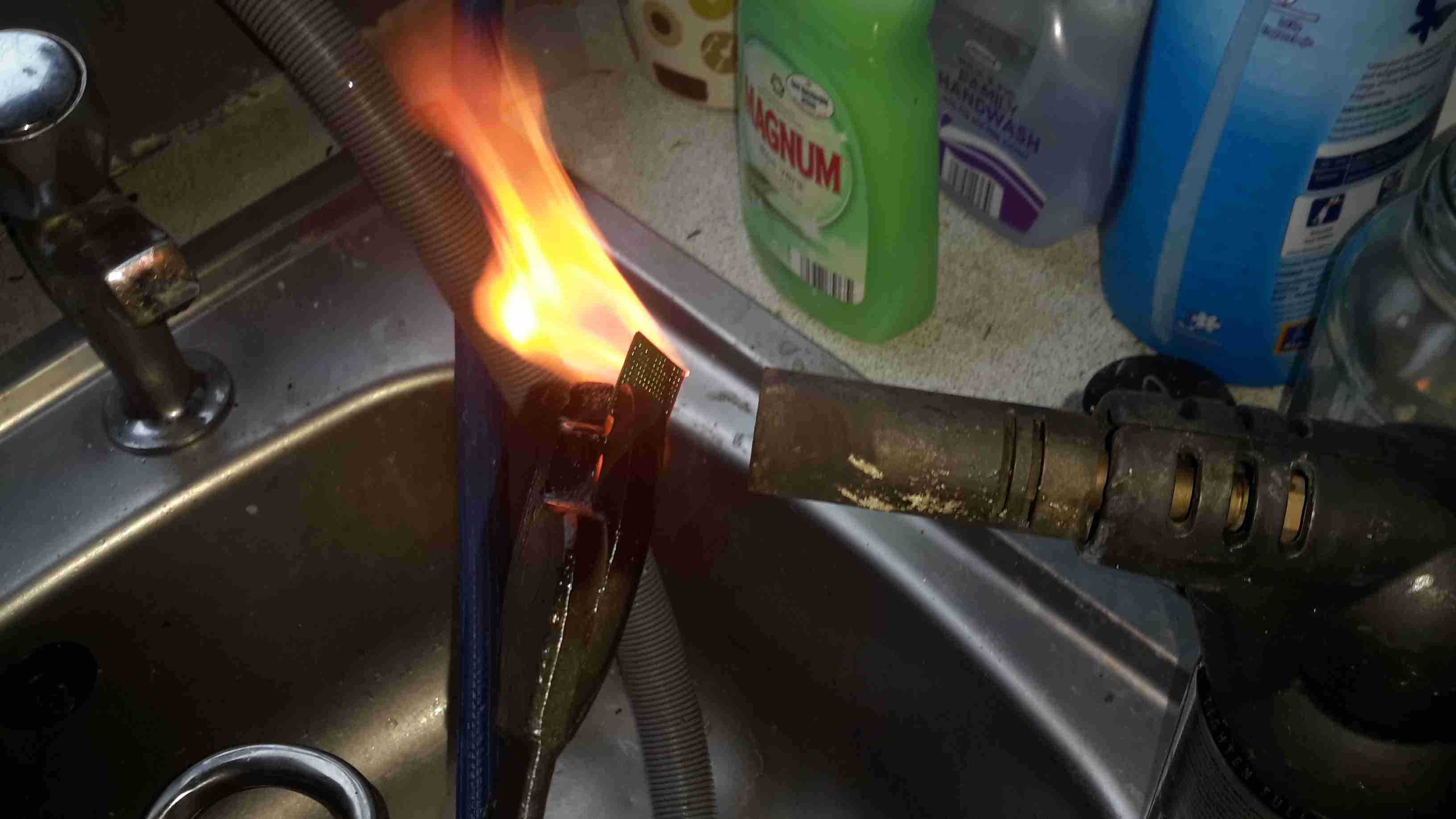
The method I use is heat based, using a Propane torch to destroy the epoxy package, without damaging the Silicon die too much.
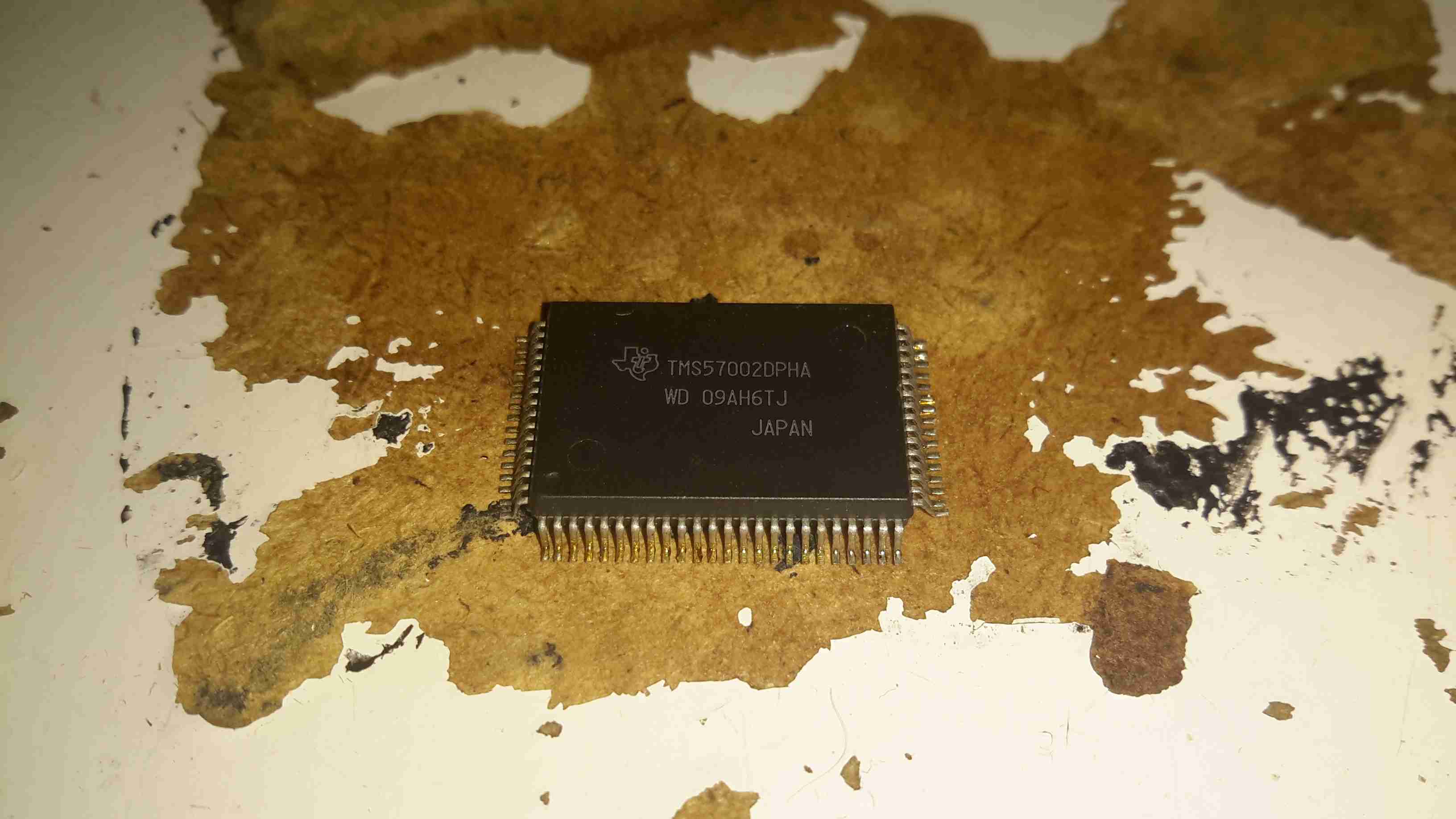
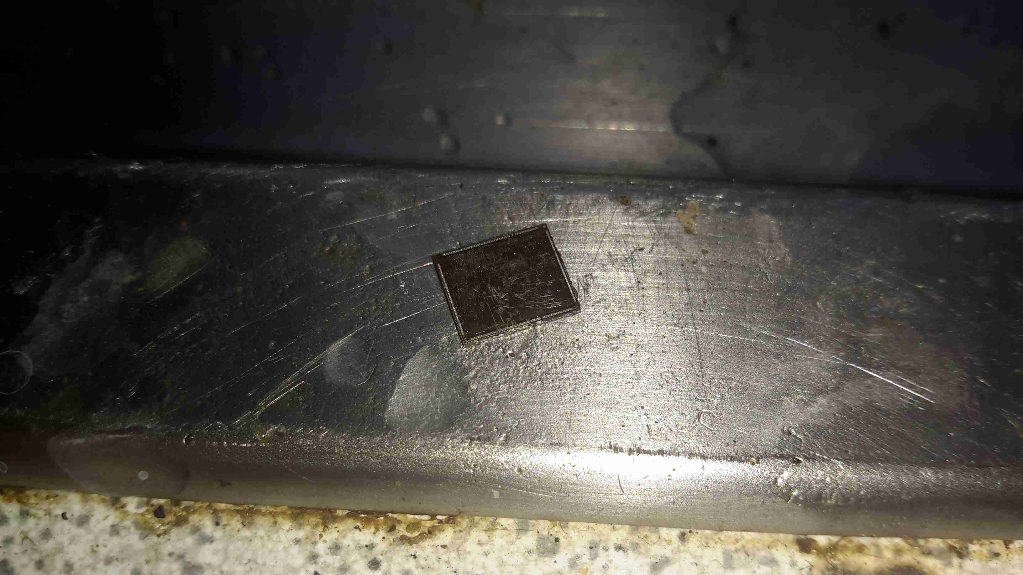
TMS57002 Audio DSP
I start off, obviously, with a desoldered IC, the one above an old audio DSP from TI. I usually desolder en-masse for this with a heat gun, stripping the entire board in one go.
FLAMES!
Next is to apply the torch to the IC. A bit of practice is required here to get the heat level & time exactly right, overheating will cause the die to oxidize & blacken or residual epoxy to stick to the surface.
I usually apply the torch until the package just about stops emitting it’s own yellow flames, meaning the epoxy is almost completely burned away. I also keep the torch flame away from the centre of the IC, where the die is located.
Breathing the fumes from this process isn’t recommended, no doubt besides the obvious soot, the burning plastic will be emitting many compounds not brilliant for Human health!
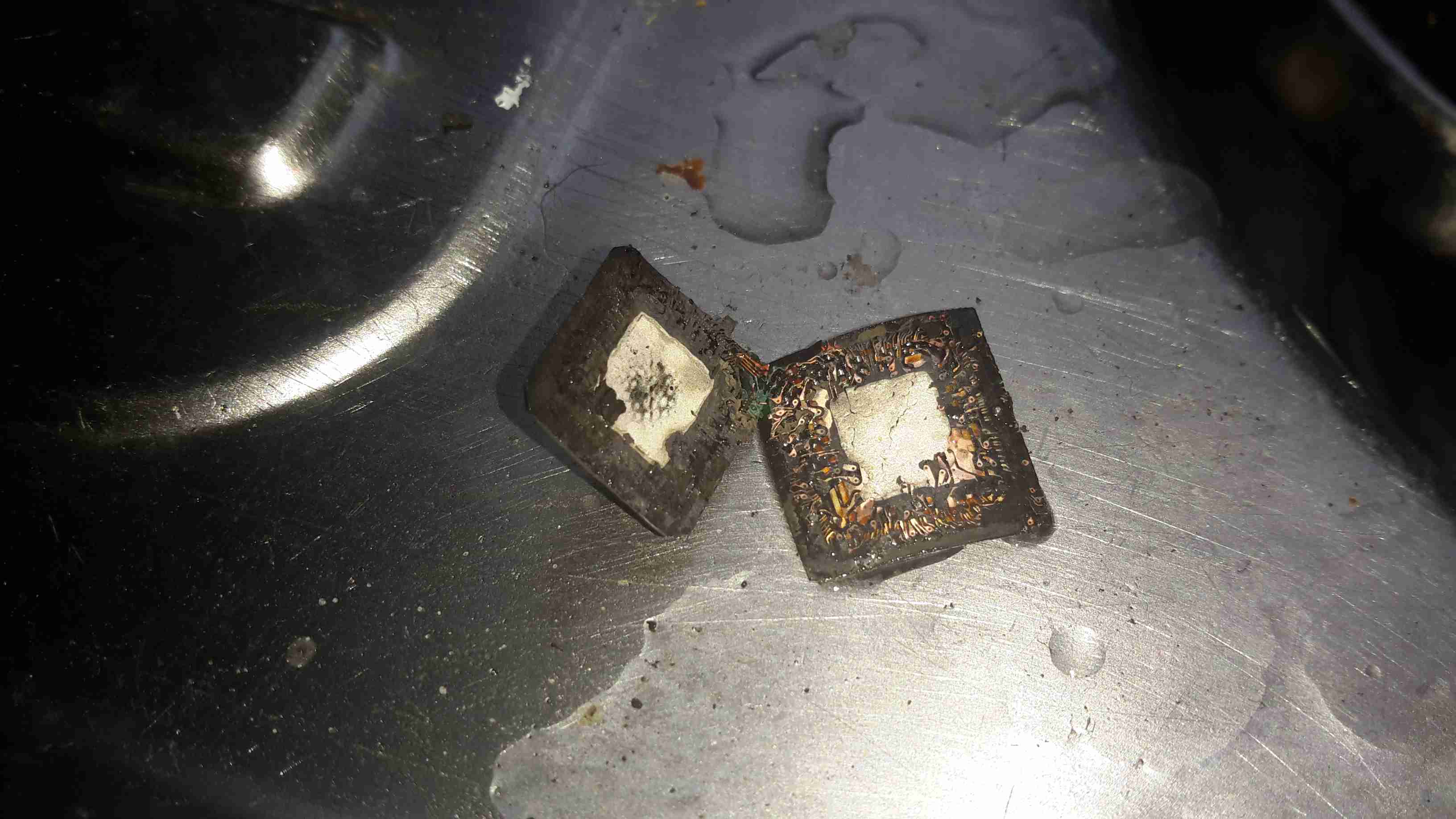
Once the IC is roasted to taste, it’s quenched in cold water for a few seconds. Sometimes this causes such a high thermal shock that the leadframe cracks off the epoxy around the die perfectly.
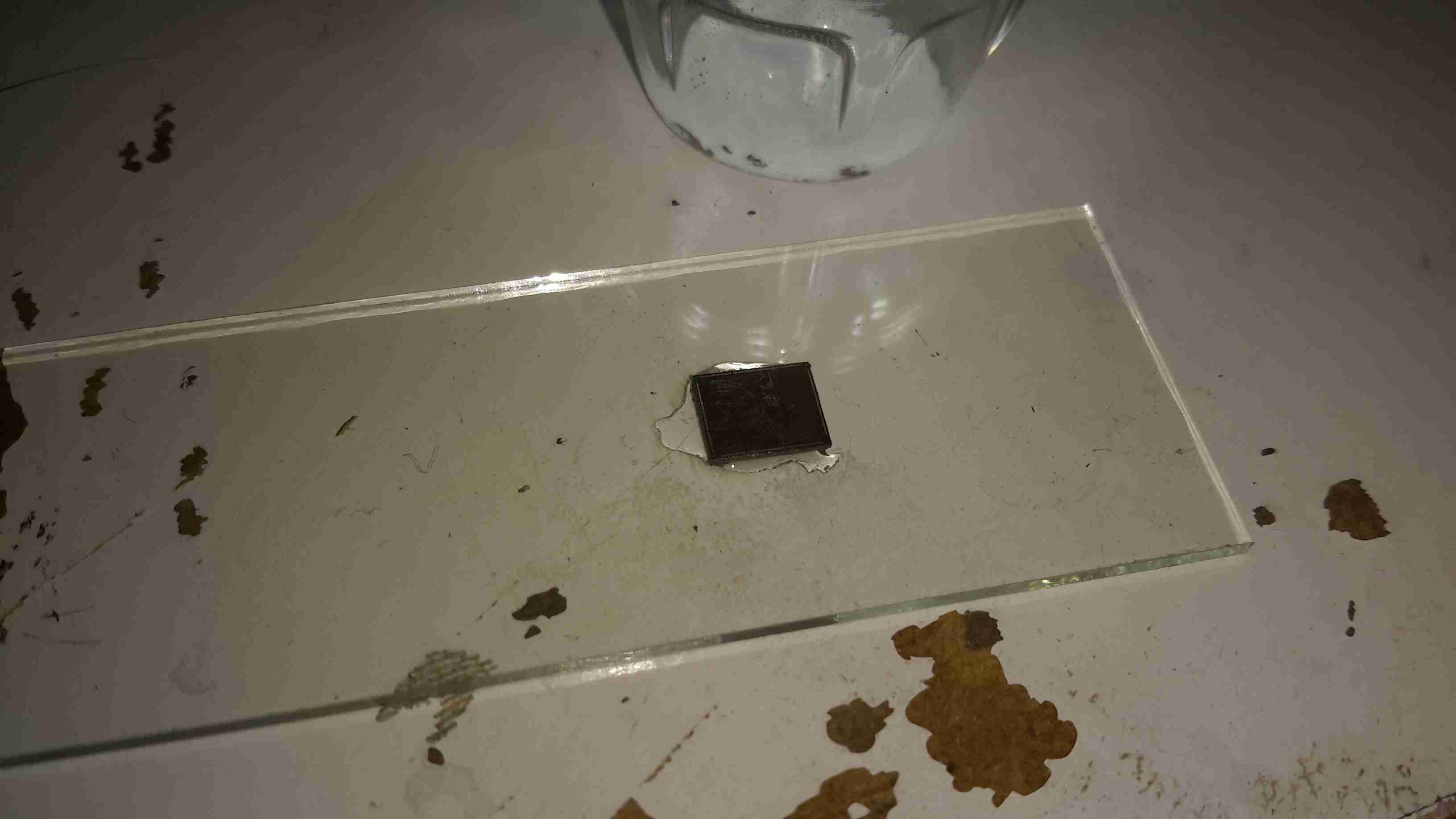
All Your Die Belong To Us
Now that the epoxy has been destroyed, it breaks apart easily, and is picked away until I uncover the die itself. (It’s the silver bit in the middle of the left half). The heat from the torch usually destroys the Silver epoxy holding the die to the leadframe, and can be removed easily from the remaining package.
Decapped
BGA packages are usually the easiest to decap, flip-chip packages are a total pain due to the solder balls being on the front side of the die, I haven’t managed to get a good result here yet, I’ll probably need to chemically remove the first layer of the die to get at the interesting bits 😉
Slide
Once the die has been rinsed in clean water & inspected, it’s mounted on a glass microscope slide with a small spot of Cyanoacrylate glue to make handling easier.
Some dies require some cleaning after decapping, for this I use 99% Isopropanol & 99% Acetone, on the end of a cotton bud. Any residual epoxy flakes or oxide stuck to the die can be relatively easily removed with a fingernail – turns out fingernails are hard enough to remove the contamination, but not hard enough to damage the die features.
Once cleaning is complete, the slide is marked with the die identification, and the photographing can begin.
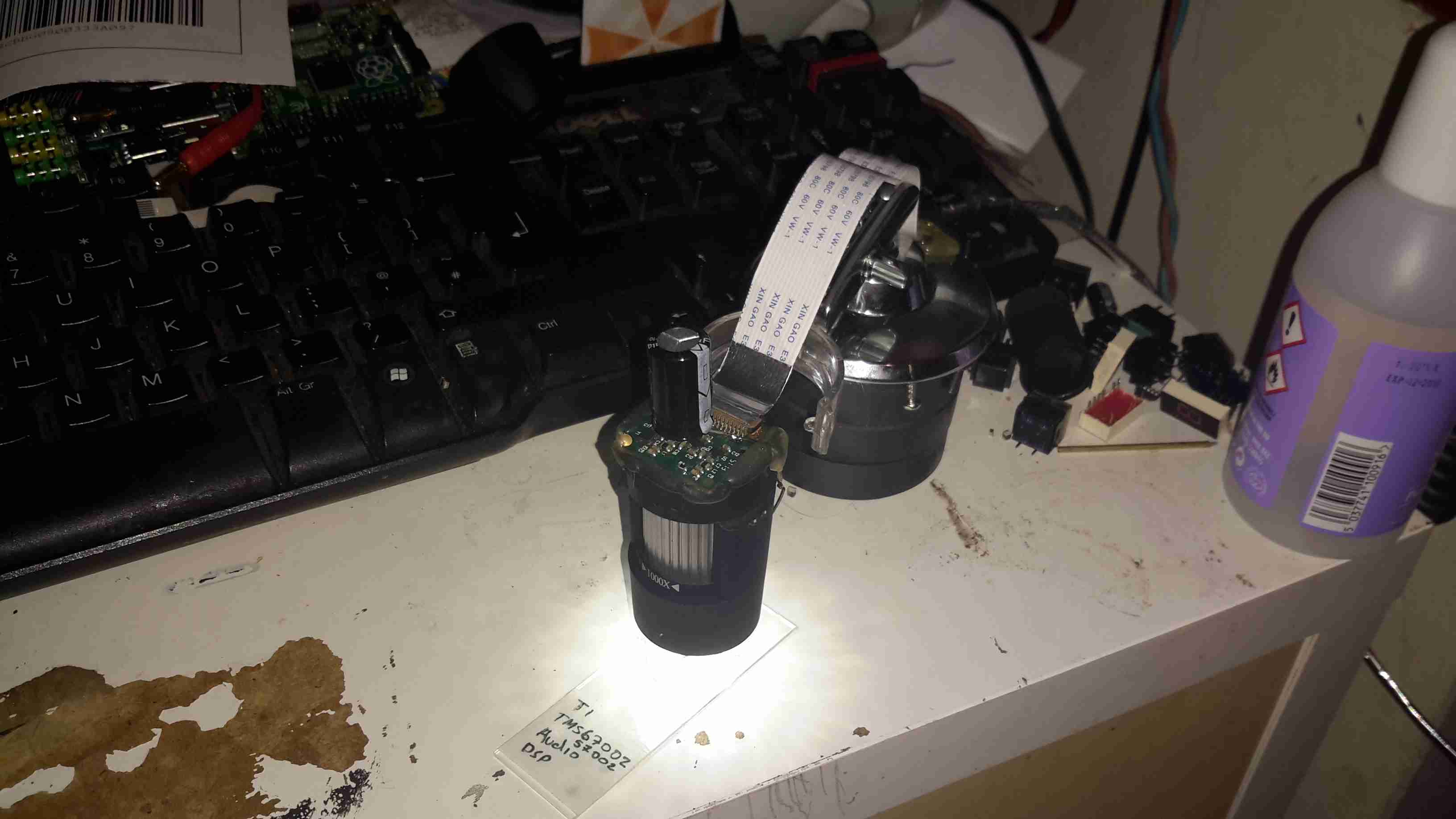
Microscope Mods
I had bought a cheap eBay USB microscope to get started, as I can’t currently afford a proper metallurgical microscope, but I found the resolution of 640×480 very poor. Some modification was required!
Modified Microscope
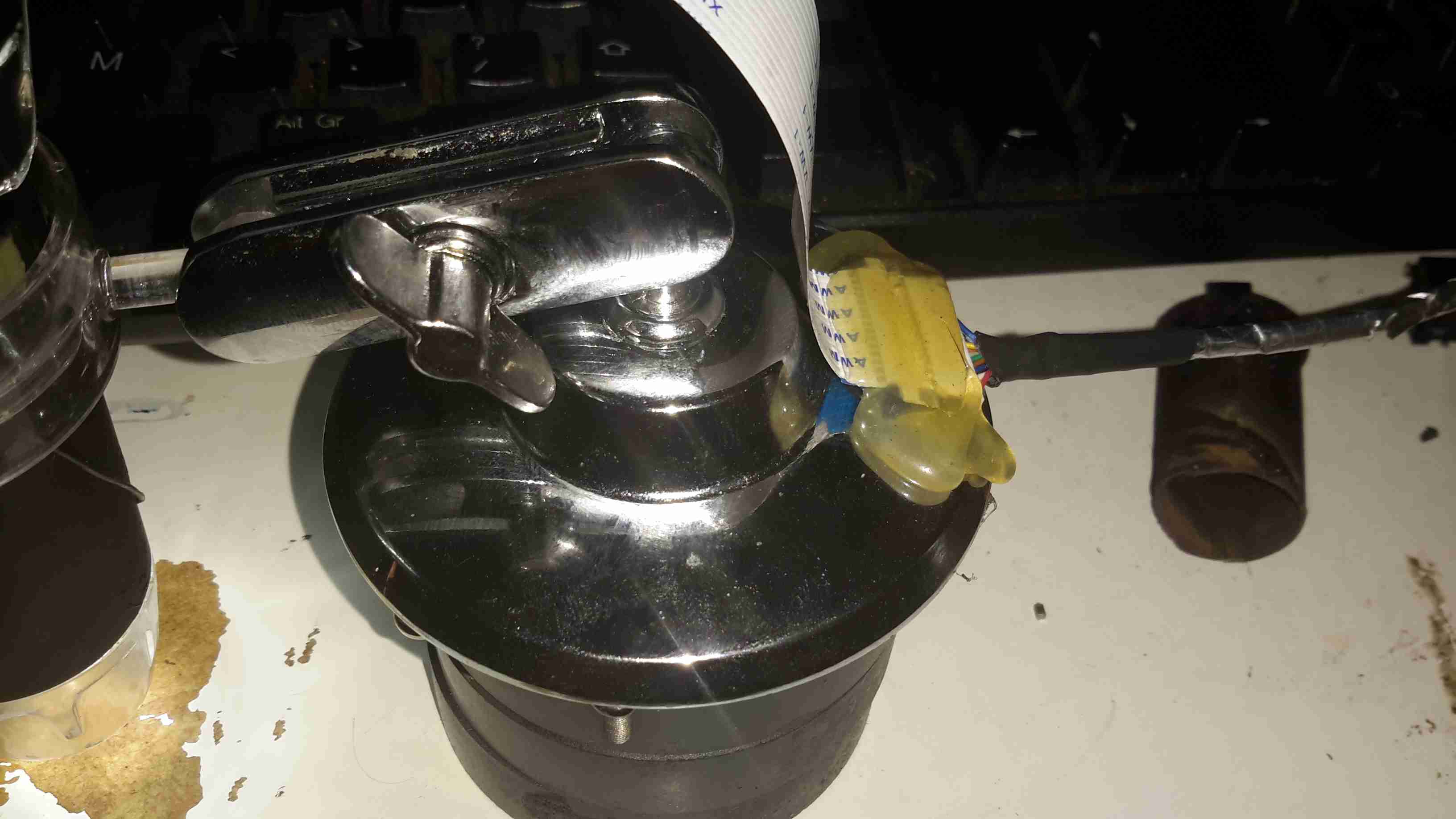
I’ve removed the original sensor board from the back of the optics assembly & attached a Raspberry Pi camera board. The ring that held the original sensor board has been cut down to a minimum, as the Pi camera PCB is slightly too big to fit inside.
The stock ring of LEDs is run direct from the 3.3v power rail on the camera, through a 4.7Ω resistor, for ~80mA. I also added a 1000µF capacitor across the 3.3v supply to compensate a bit for the long cable – when a frame is captured the power draw of the camera increases & causes a bit of voltage drop.
The stock lens was removed from the Pi camera module by careful use of a razor blade – being too rough here *WILL* damage the sensor die or the gold bond wires, which are very close to the edge of the lens housing, so be gentle!
Mounting Base
The existing mount for the microscope is pretty poor, so I’ve used a couple of surplus ceramic ring magnets as a better base, this also gives me the option of raising or lowering the base by adding or removing magnets.
To get more length between the Pi & the camera, I bought a 1-meter cable extension kit from Pi-Cables over at eBay, cables this long *definitely* require shielding in my space, which is a pretty aggressive RF environment, or interference appears on the display. Not surprising considering the high data rates the cable carries.
The FFC interface is hot-glued to the back of the microscope mount for stability, for handheld use the FFC is pretty flexible & doesn’t apply any force to the scope.
Die Photography
Since I modified the scope with a Raspberry Pi camera module, everything is done through the Pi itself, and the raspistill command.
Pi LCD
The command I’m currently using to capture the images is:
raspistill -ex auto -awb auto -mm matrix -br 62 -q 100 -vf -hf -f -t 0 -k -v -o CHIPNAME_%03d.jpg
This command waits between each frame for the ENTER key to be pressed, allowing me to position the scope between shots. Pi control & file transfer is done via SSH, while I use the 7″ touch LCD as a viewfinder.
The direct overhead illumination provided by the stock ring of LEDs isn’t ideal for some die shots, so I’m planning on fitting some off-centre LEDs to improve the resulting images.
Image Processing
Obviously I can’t get an ultra-high resolution image with a single shot, due to the focal length, so I have to take many shots (30-180 per die), and stitch them together into a single image.
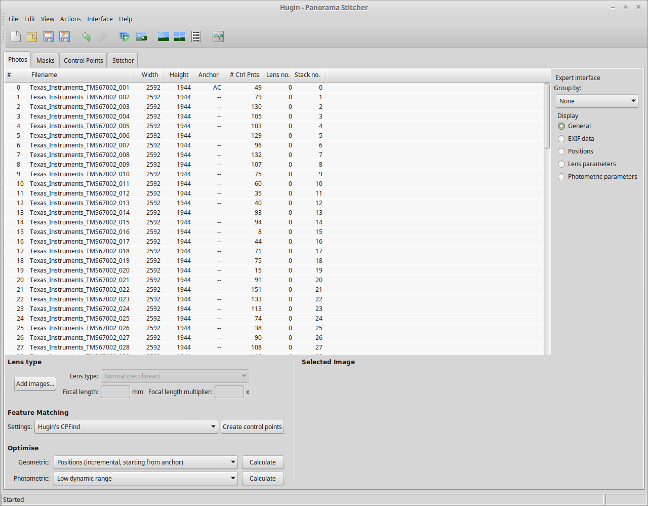
For this I use Hugin, an open-source panorama photo stitching package.
Hugin
Here’s Hugin with the photos loaded in from the Raspberry Pi. To start with I use Hugin’s built in CPFind to process the images for control points. The trick with getting good control points is making sure the images have a high level of overlap, between 50-80%, this way the software doesn’t get confused & stick the images together incorrectly.
Optimiser
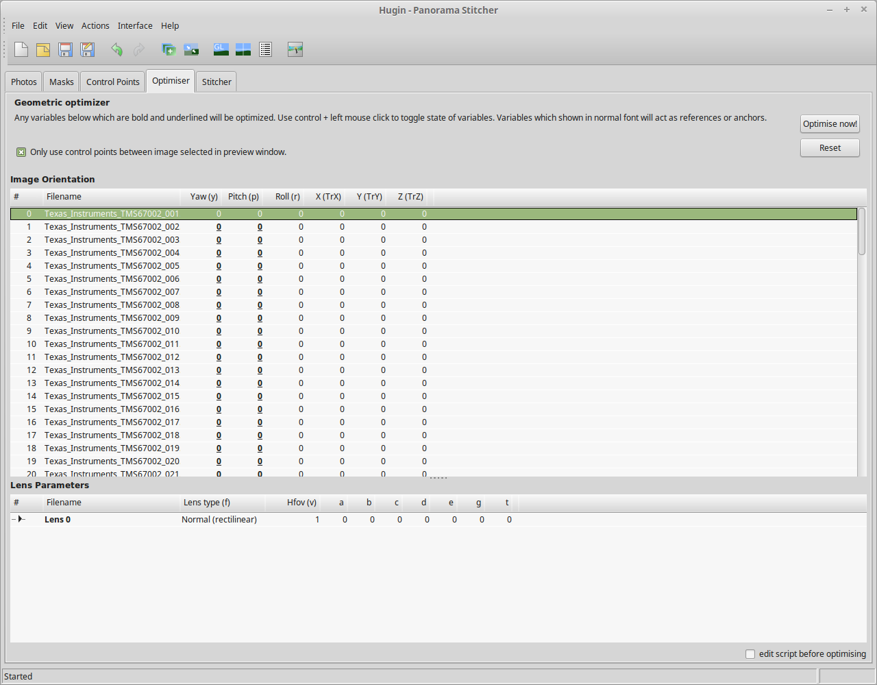
After the control points are generated, which for a large number of high resolution images can take some time, I run the optimiser with only Yaw & Pitch selected for all images.
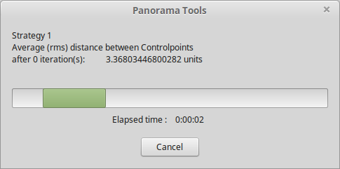
Optimising
If all goes well, the resulting optimisation will get the distance between control points to less than 0.3 pixels.
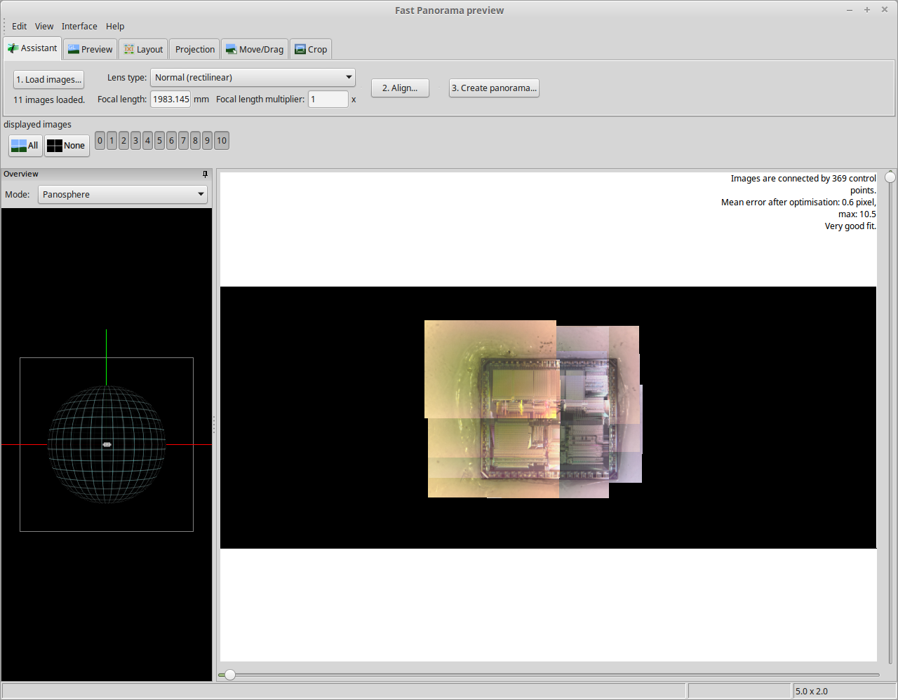
Panorama Preview
After the control points & optimisation is done, the resulting image can be previewed before generation.
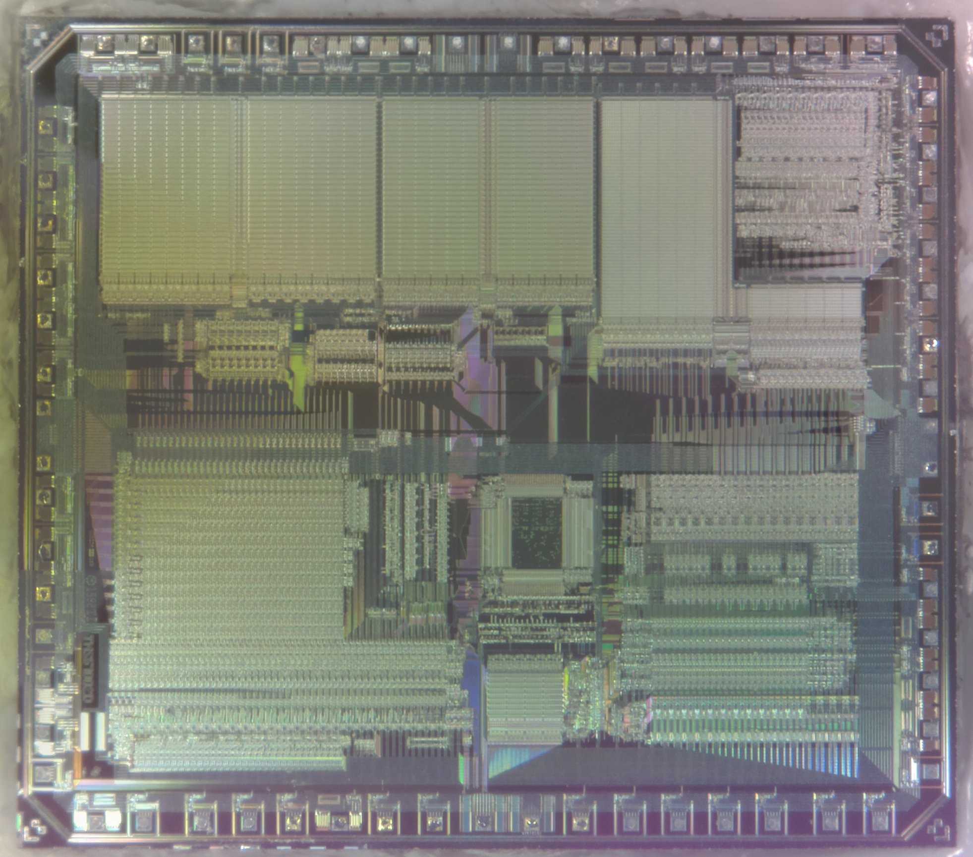
Texas Instruments TMS67002
After all the image processing, the resulting die image should look something like the above, with no noticeable gaps.
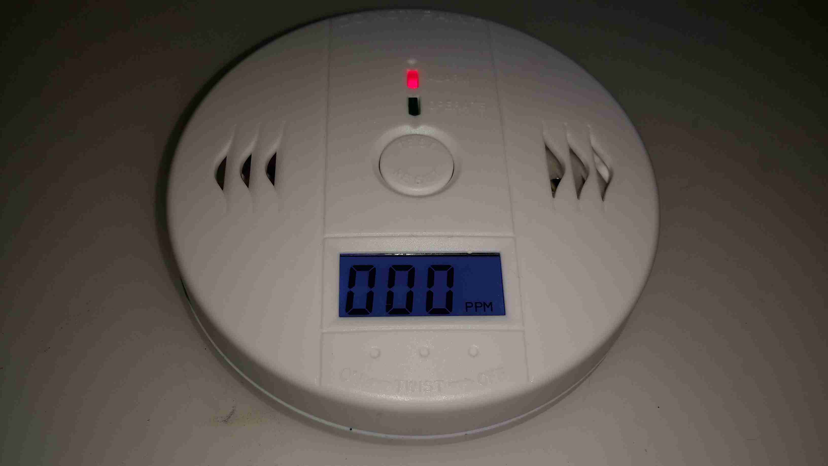
I was looking around eBay for decent deals on a branded CO alarm, and came across these for next to no money, so I thought I’d grab one just to see how bad they could be.
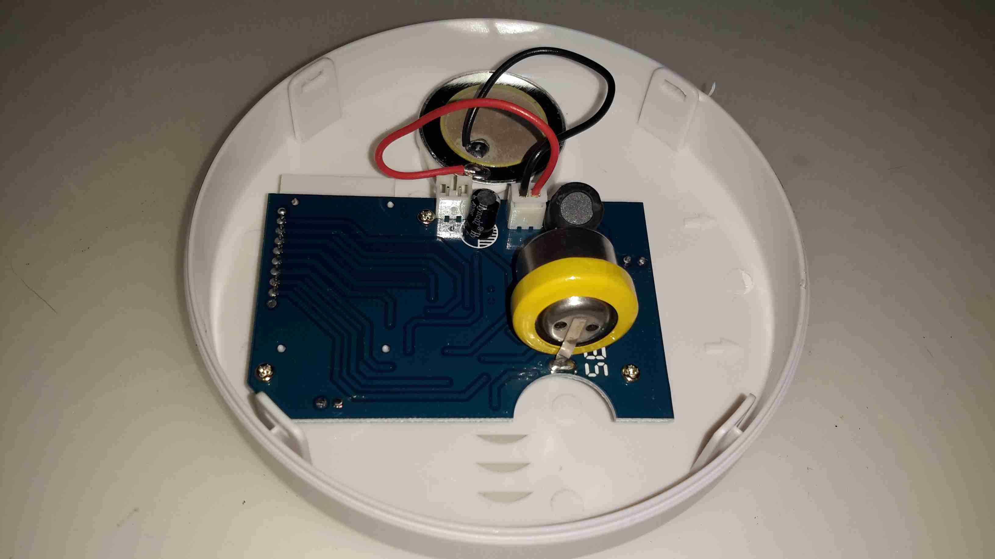
Alarm Opened
Popping the casing open shows the very small circuit board inside, with the CO sensor cell on the right. I can’t find any manufacturer information on this cell, nor can I find a photo of anything similar on the intertubes, so no specifications there. The other parts are pretty standard, a Piezo sounder & it’s associated step-up transformer to increase the loudness.
Sensor Closeup
The sensor cell has the usual opening in the end to allow entry of gas.
Main PCB
The other side of the board doesn’t reveal much, just an LCD, a couple of LEDs, a pair of transistors, Op-Amp for the sensor & a main microcontroller.
MCU
The microcontroller isn’t marked unfortunately. It’s not had the number scrubbed off, it’s just never been laser marked with a part number. Above the micro is a SOT-23 LM321 low-power Op-Amp which does the signal conditioning for the CO sensor.
I tried to make this alarm trigger with the exhaust from the Eberspacher heater, which on a well-made branded alarm registered a reading of 154ppm after a few minutes. In the case of this alarm though, I couldn’t make it trigger at all, no matter how long I exposed it to hydrocarbon exhaust gases. I won’t be trusting this one then!
Nothing quite like a piece of safety equipment that doesn’t work correctly from new!
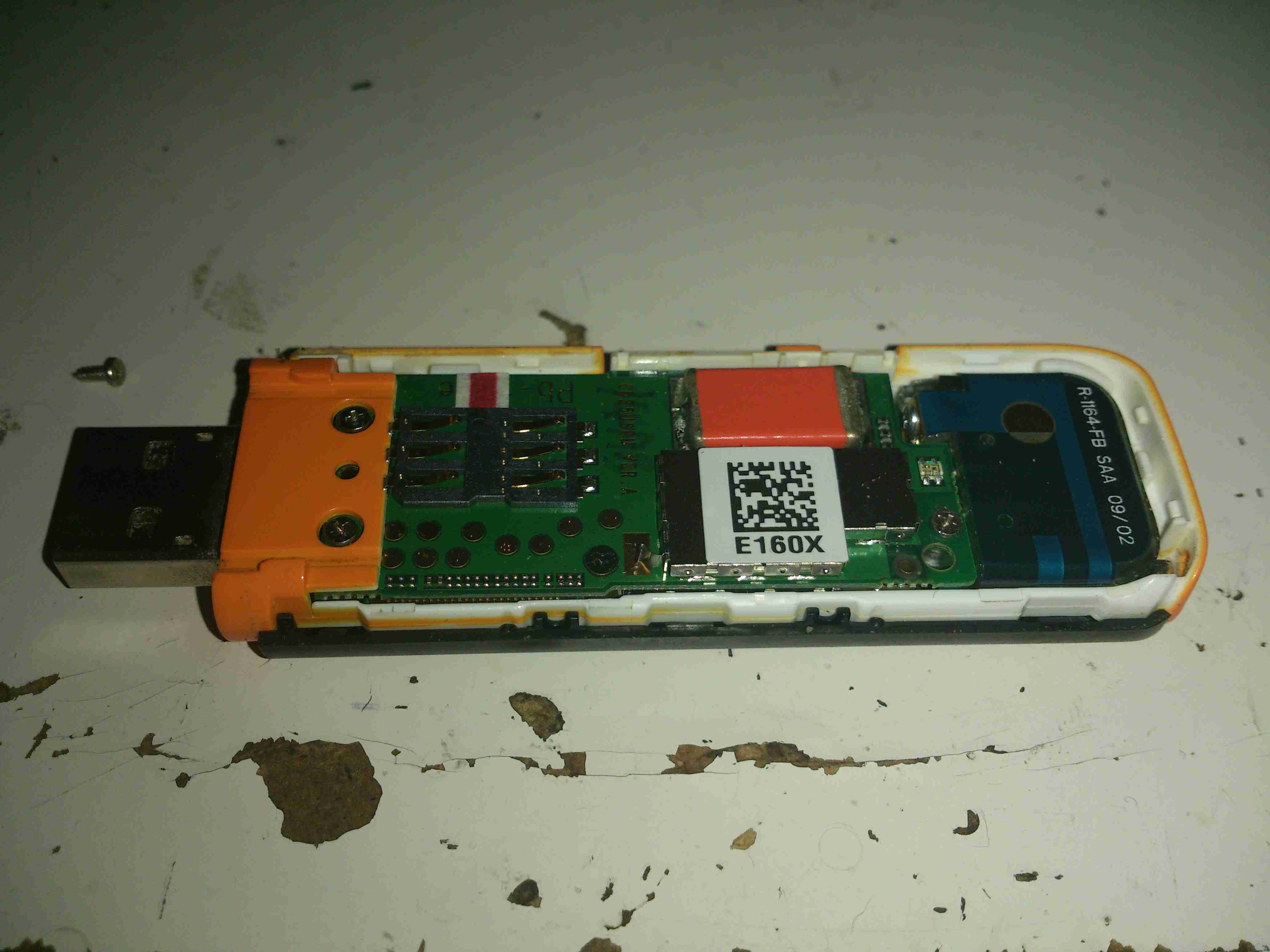
Here’s an old HDSPA 3G USB modem stick that I got with a mobile phone contact many years ago. As it’s now very old tech, and I have a faster modem, not to mention that I’m no longer with Orange (Robbing <expletive>), here’s a teardown of the device!
Cover Removed
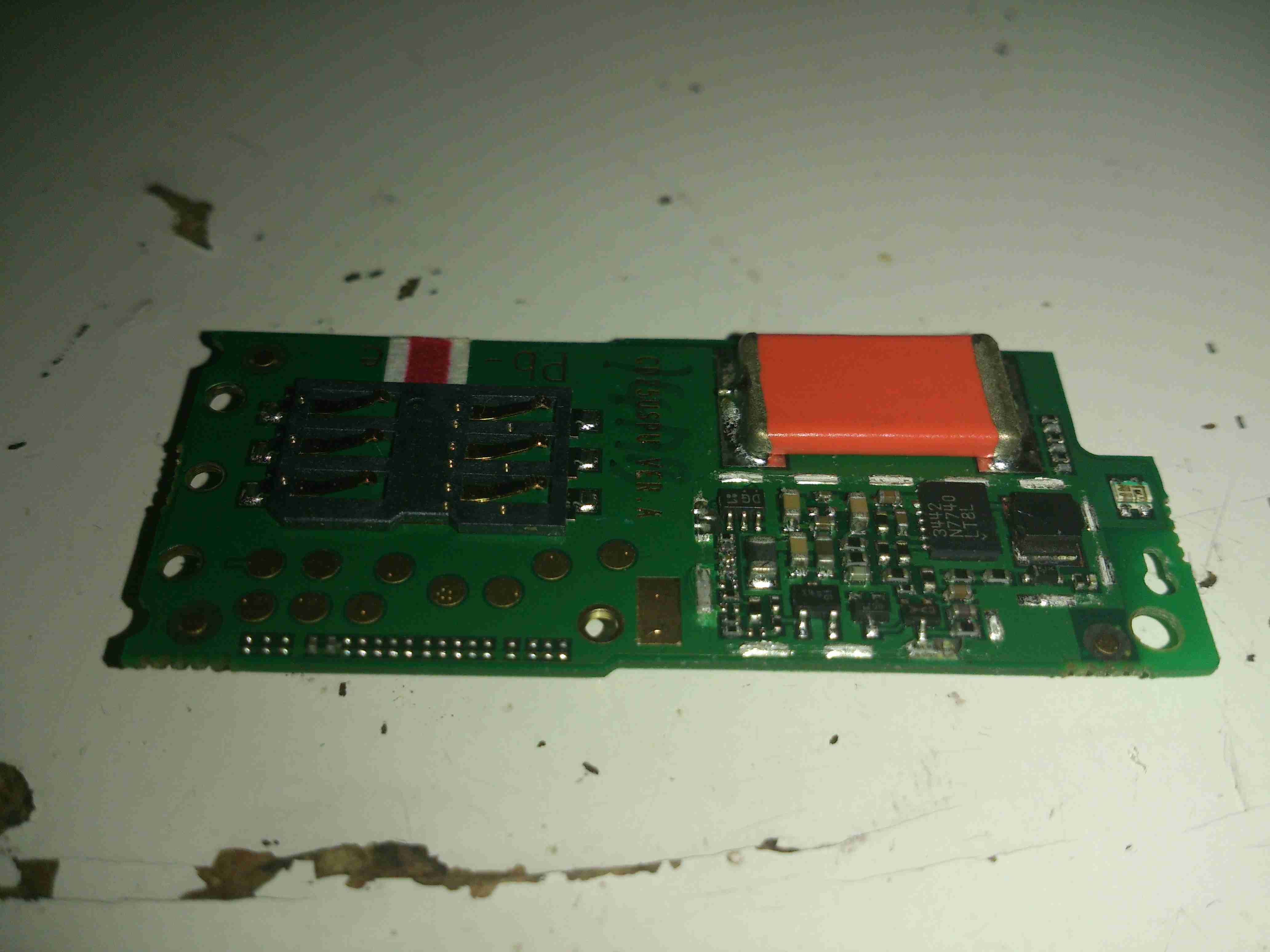
The top shell is just clipped into place, while a pair of very small screws hold down the orange piece at left to hold the PCB stack in the casing. Not much to see here, but it’s clear that there’s a lot crammed into a very small space.
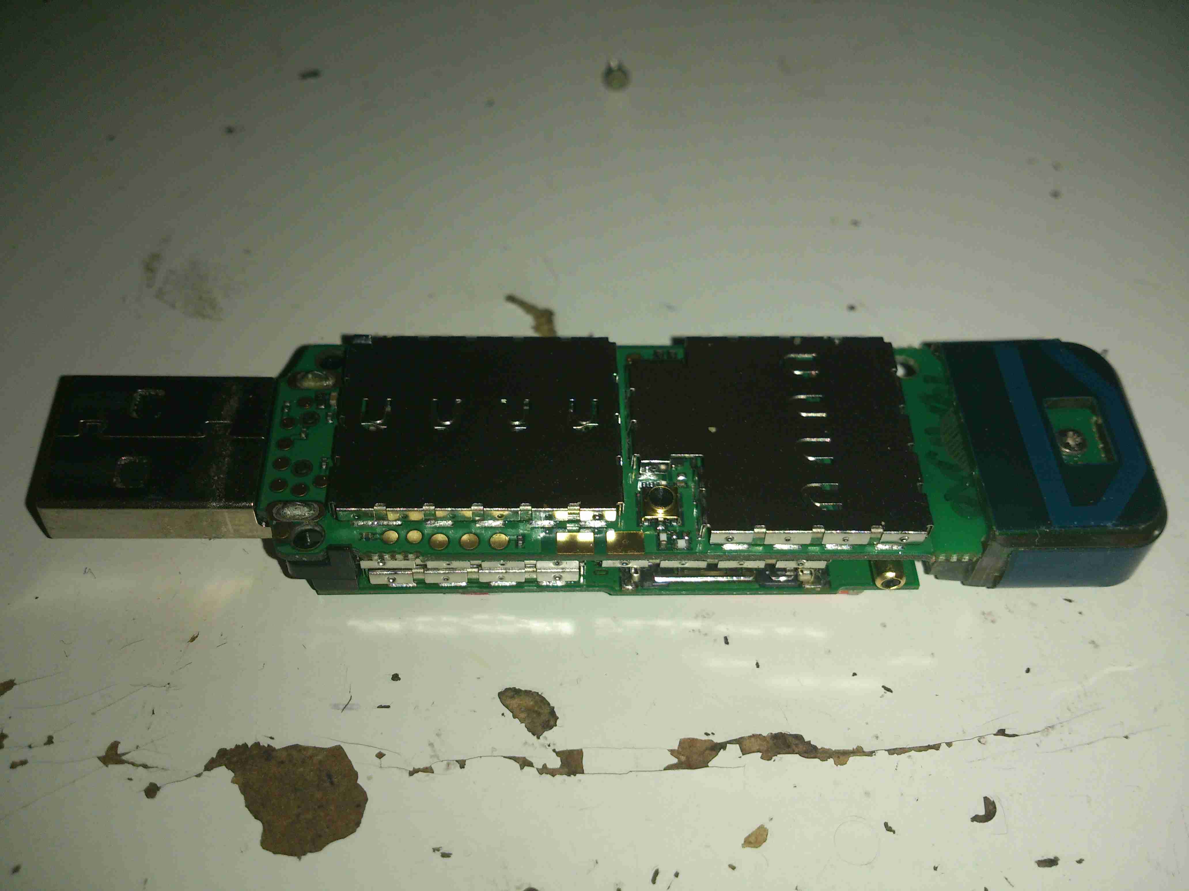
PCB Assembly
Here’s the PCB stack removed from the outer casing. The main antenna is on the right, attached with another small screw. Every IC on the boards is covered with an RF can. No problems there, pliers to the rescue!
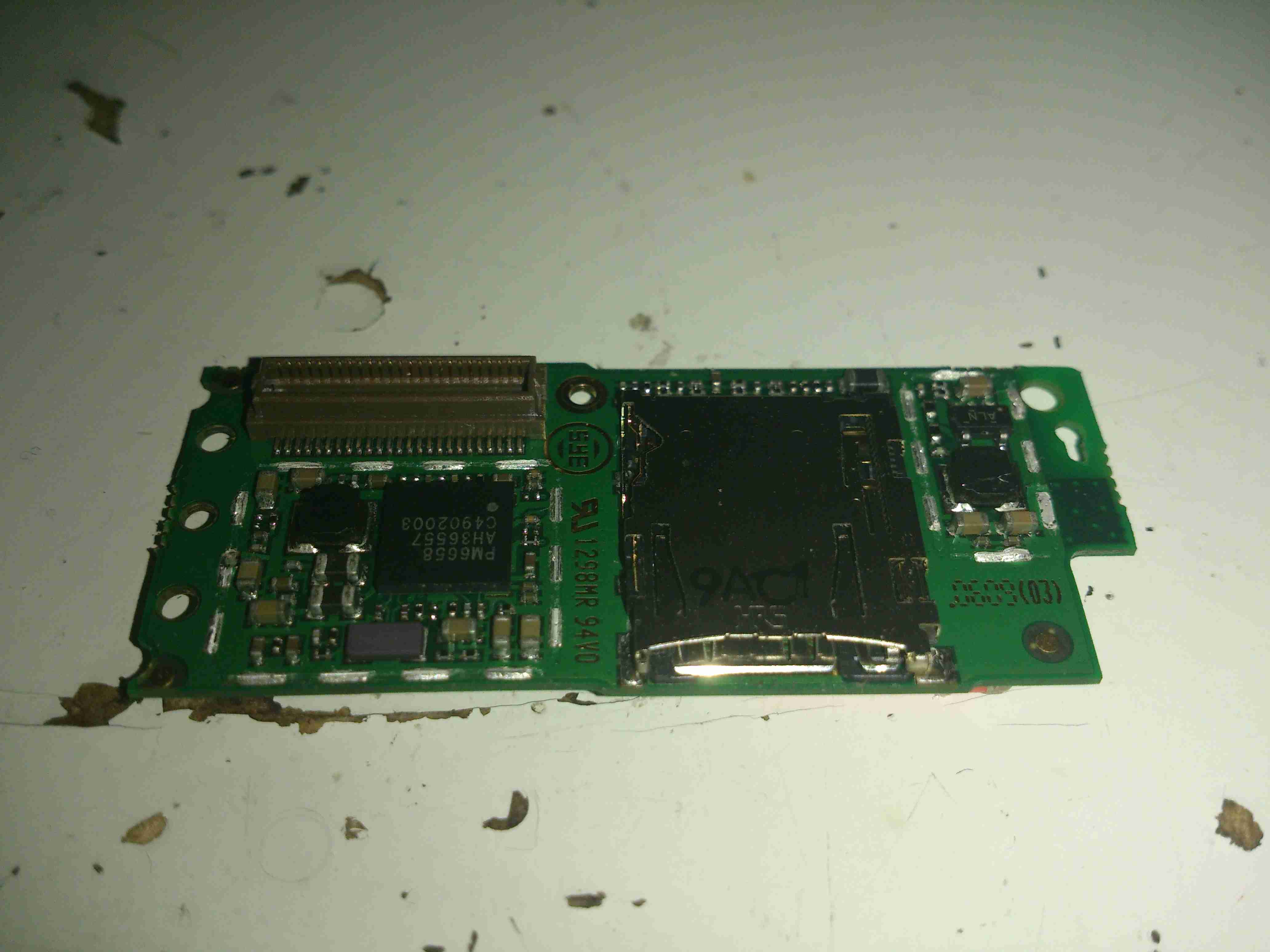
SD Card Slot
Here’s the top PCB, all the shields have been removed. On the left is a Qualcomm PM6658 Power Management IC with integrated USB transceiver. This is surrounded by many of the power management circuits.
The integrated SD Card slot is on the right side. with what looks to be a local switching regulator for supply voltage. This might also provide the SIM card with it’s power supply.
PSU & SIM Contacts
The other side of the top board reveals more power management, with another switching regulator, and a truly massive capacitor at the top edge. I’m guessing this is a solid Tantalum.
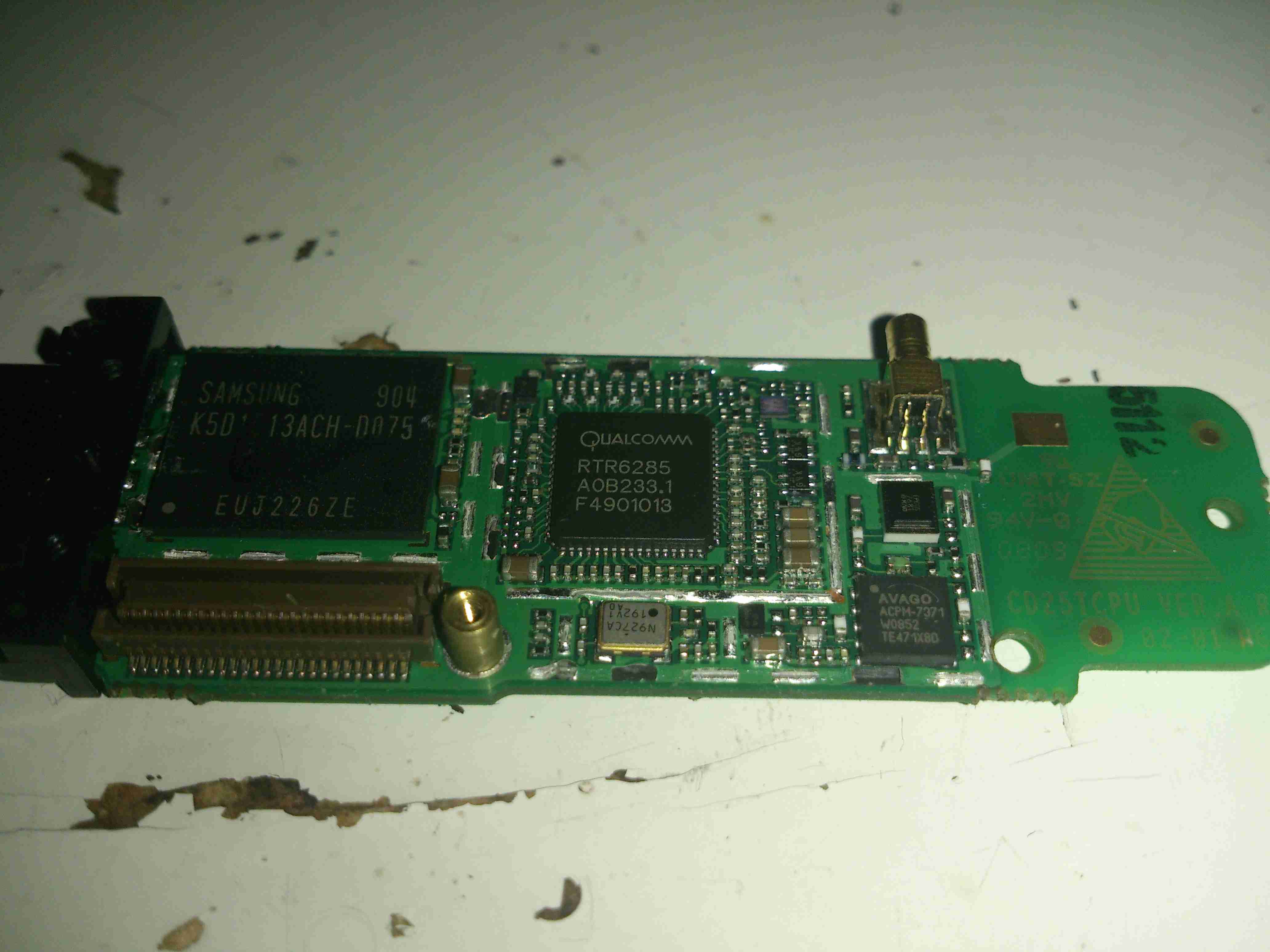
Main Chipset PCB
The other PCB holds the main chipset & RF circuits. On the left here is a Samsung MCP K5D1G13ACH IC. This one is a multiple chip package, having 1Gbit of NAND Flash & 512Mbit of mobile SDRAM.
To it’s right is a Qualcomm RTR6285 RF Transceiver. This IC supports multiband GSM/EDGE/UMTS frequencies & also has a GPS receive amplifier included.
At bottom right is an Avago ACPM7371 Wide-Band 4×4 CDMA Power Amplifier. The external antenna connector is top right.
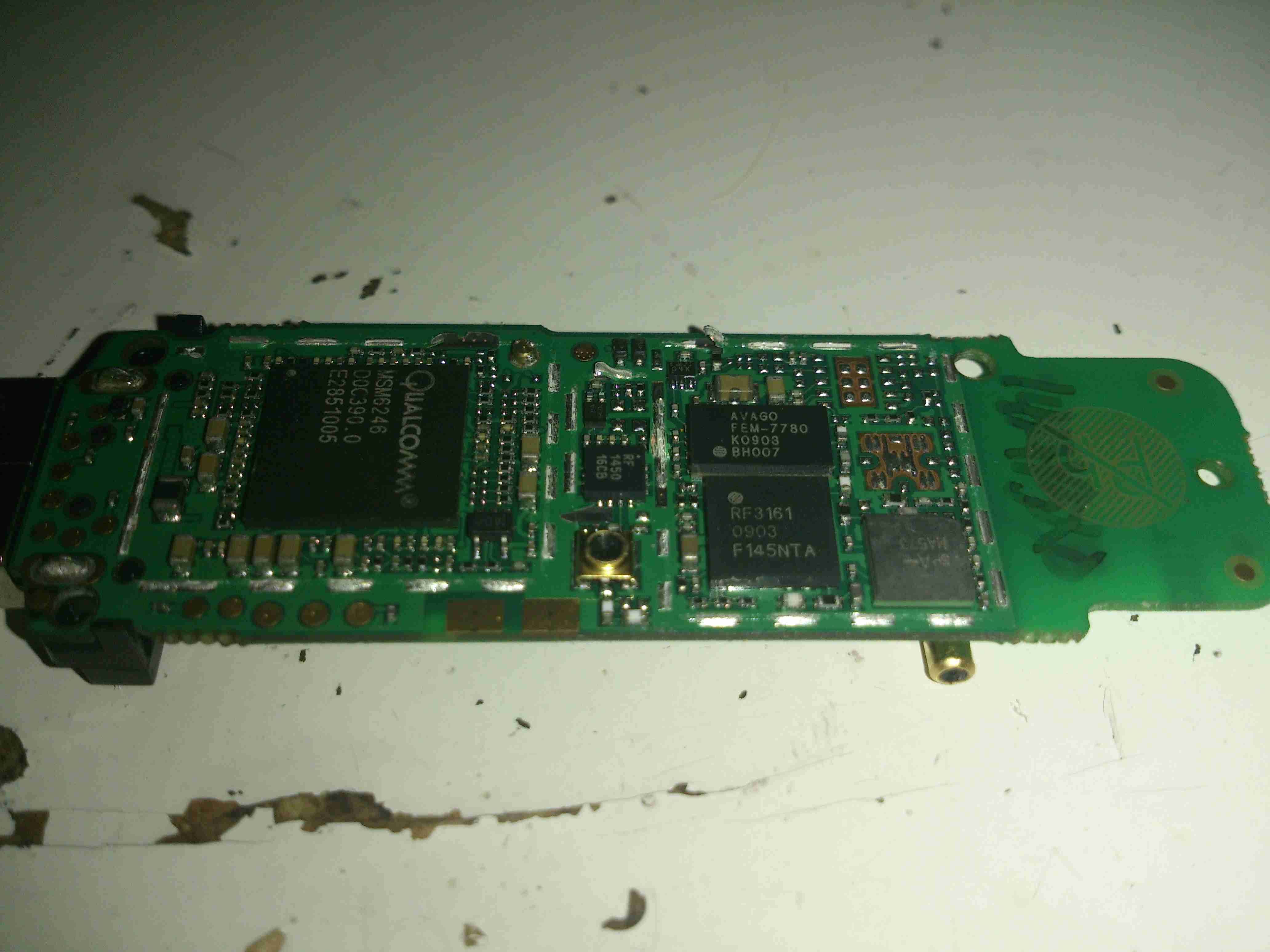
Main Chipset PCB Reverse
On the other side of the main PCB is a Qualcomm MSM6246 Baseband processor. Not sure about this one as I can’t find anything resembling a datasheet. Another micro-coax connector is in the centre, probably for factory test purposes, as it’s not accessible from the outside.
Just above the coax connector is a Qorvo RF1450 SP4T (single-pole 4-throw) High Power (34.5dBm) GSM RF Switch.
Upper right is an Avago FEM-7780 UMTS2100 4×7 Front End Module.
Under that is an RFMD RF3163 Quad-Band RF Power Amplifier Module.
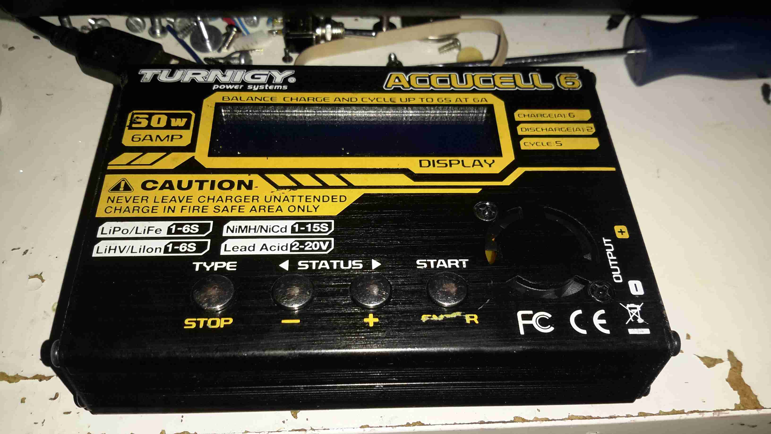
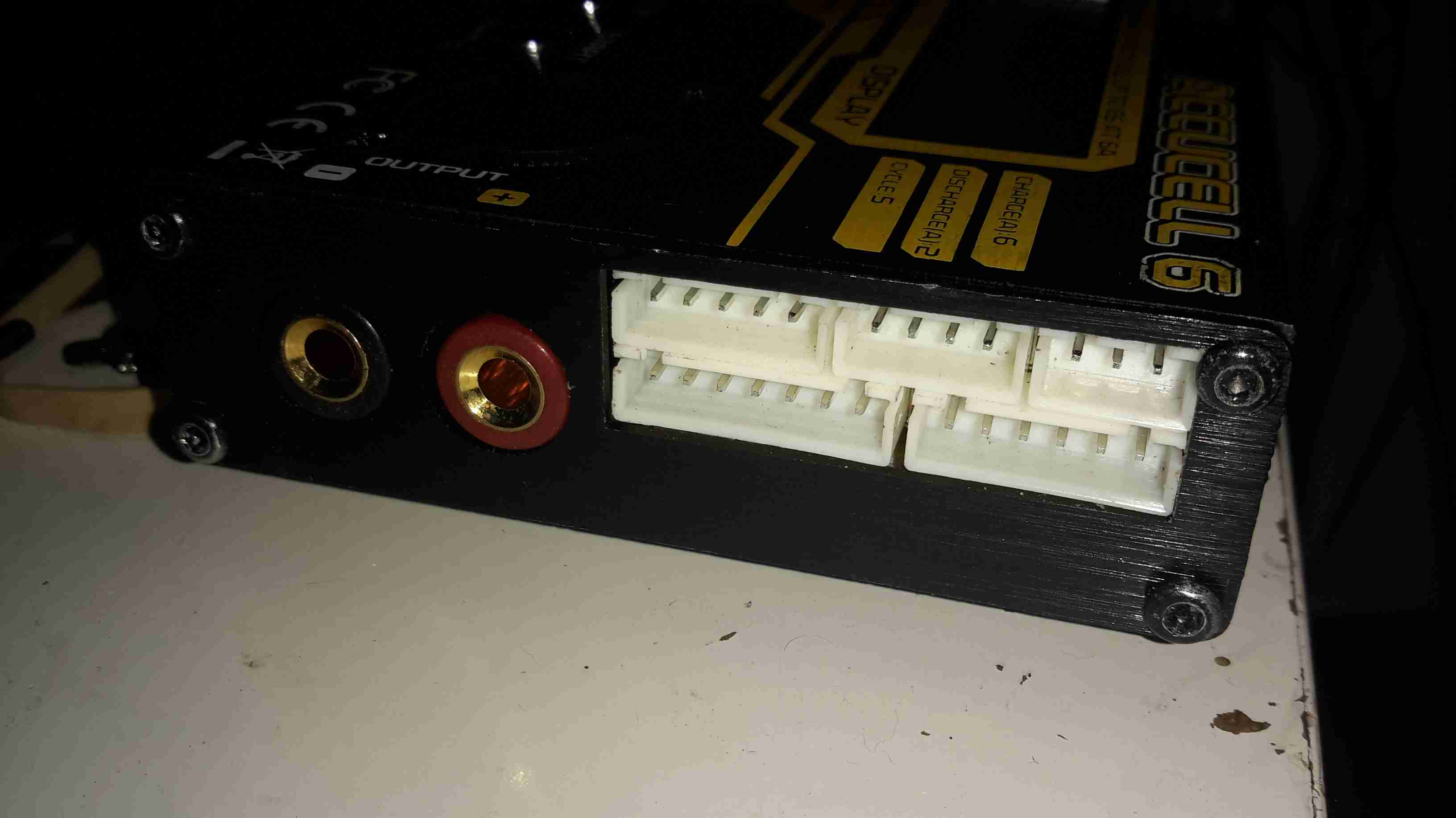
A lot of the electronics I use & projects I construct use batteries, mainly of the lithium variety. As charging this chemistry can be a little explosive if not done correctly, I decided a proper charger was required. This charger is capable of handling packs up to 6 cells for Lithium, and up to 20v for lead-acids.
External Connections
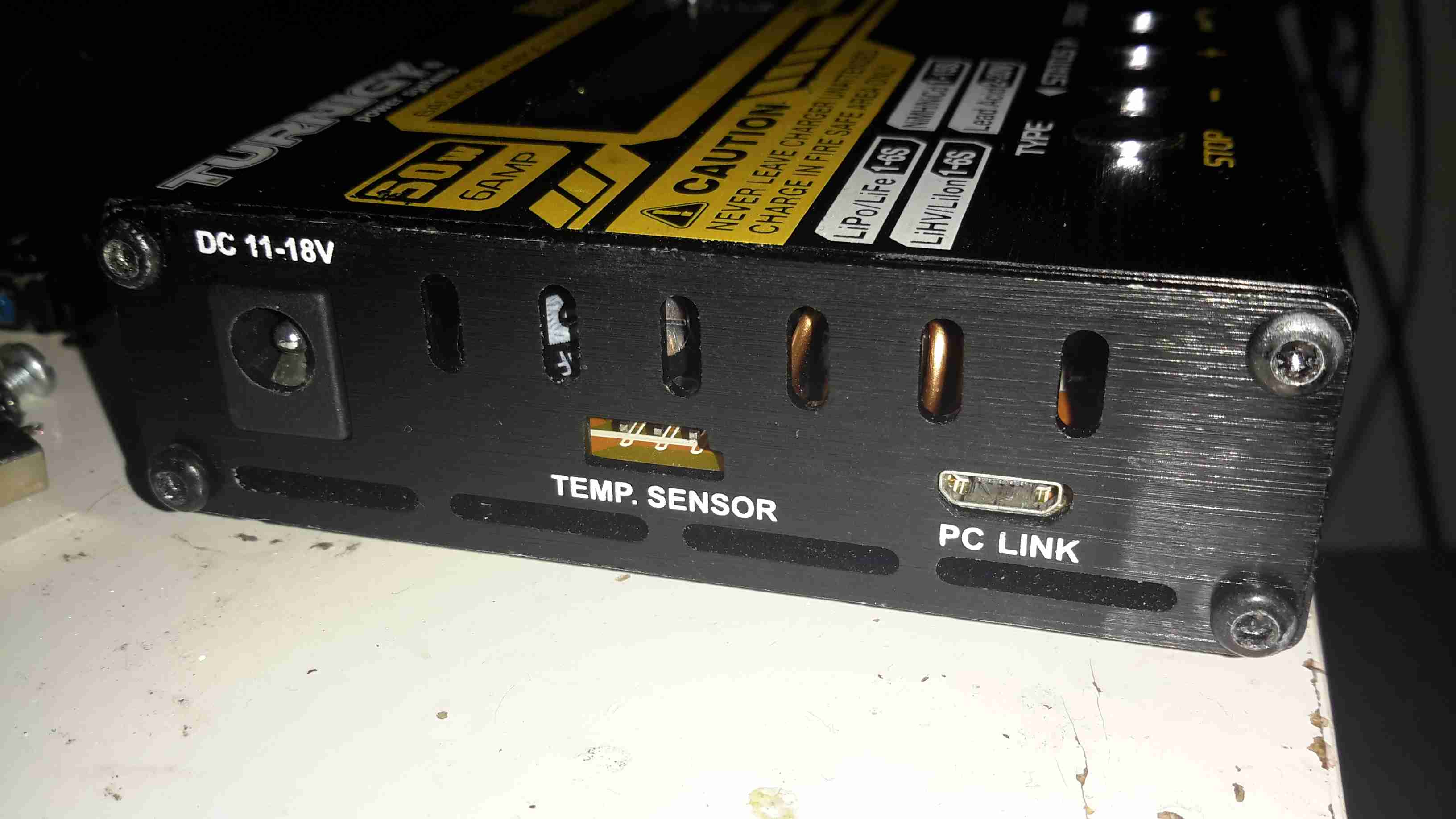
The usual DC input barrel jack on the left, with an external temp sensor for fast charging NiCd/NiMH chemistry batteries. The µUSB port registers under Linux as USB HID, probably so drivers aren’t required. Unfortunately the software is Windows only, but it doesn’t provide anything handy like charging graphs or stats. Just a way to alter settings & control charging from a PC. On other versions of this charger there’s a setting to change the temp sensor port into a TTL serial output, which would be much handier.
Output & Balance
The other side of the charger has the main DC output jacks & the pack balancing connections.
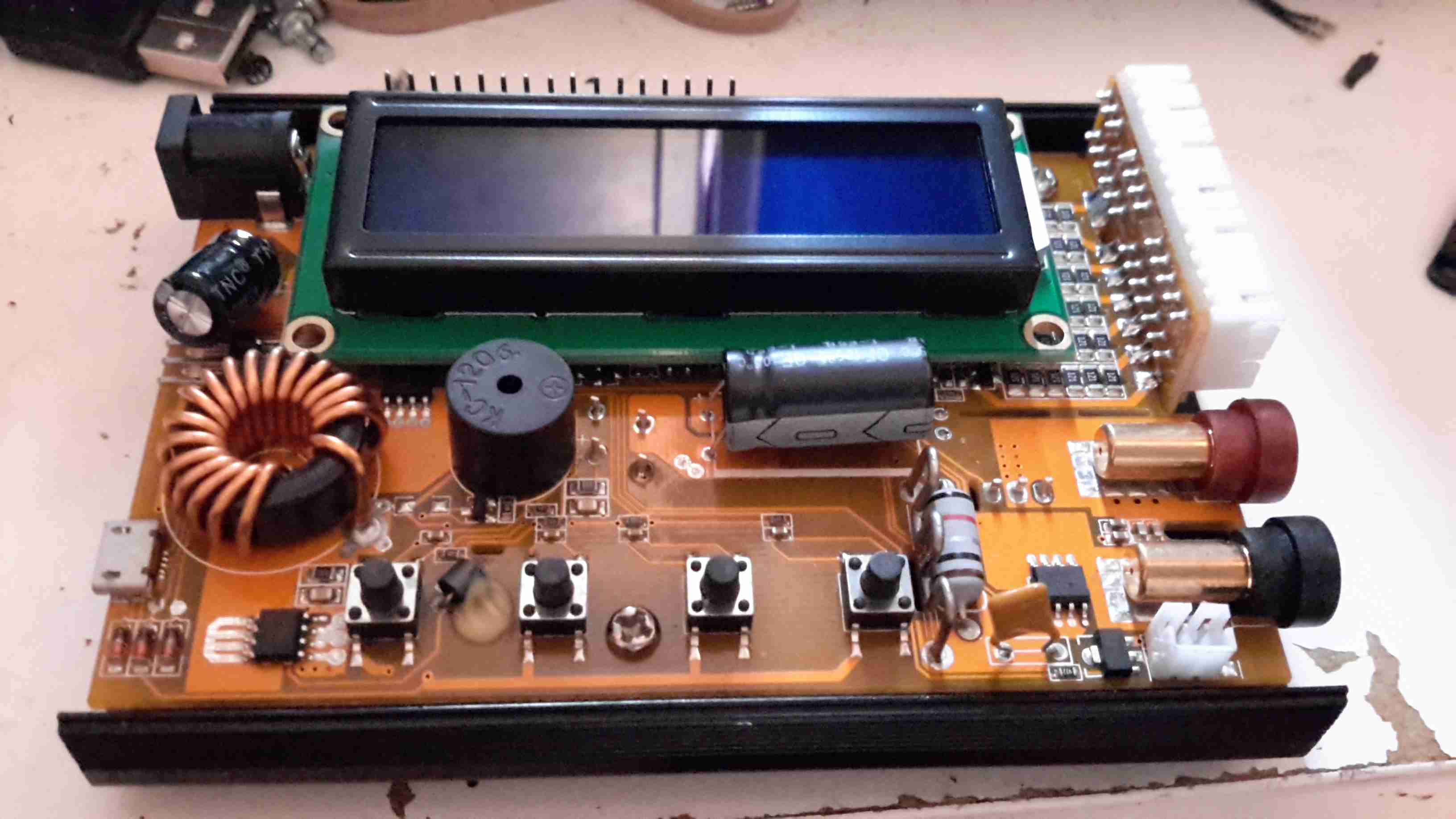
Cover Removed
Here’s the top cover removed from the charger, showing most of the internals. A standard HD44780 LCD provides the user interface, the CPU & it’s associated logic is hidden under there somewhere.
The PCB has nice heavy tracks to handle the 6A of current this charger is capable of.
Balancing Network
The output side of the board. Here the resistive pack balancing network can be seen behind the vertical daughter board holding the connectors, along with the output current shunt between the DC output banana jacks & the last tactile button.
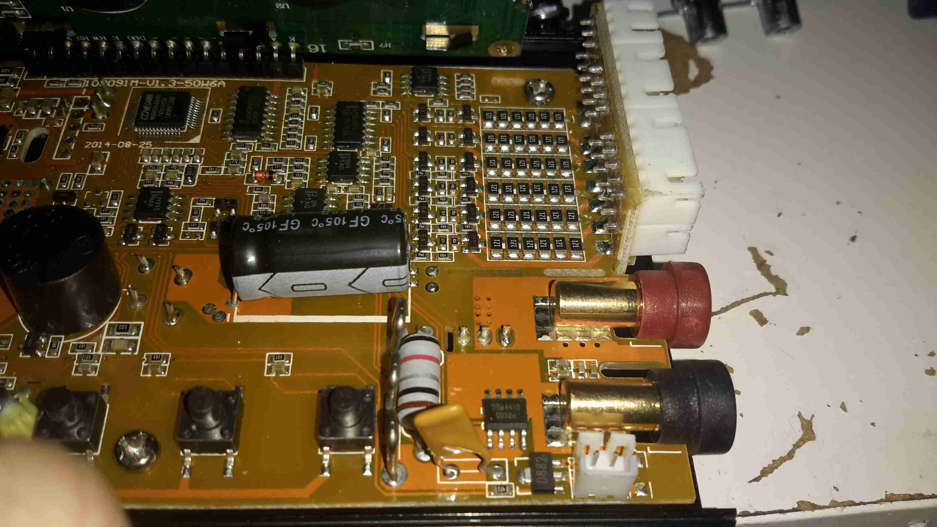
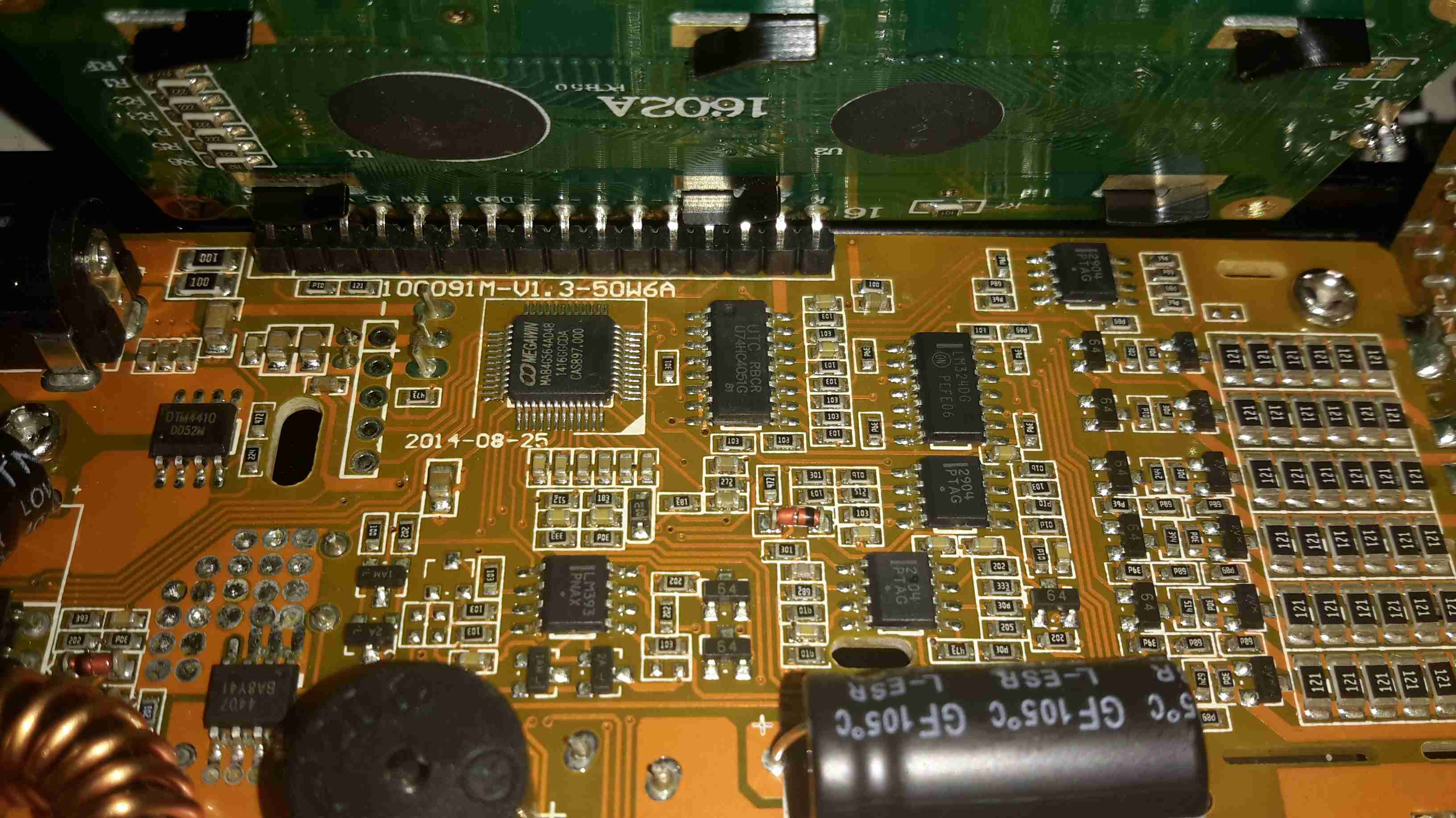
Main Logic
Unfortunately the LCD is soldered directly to the board, and my desoldering tool couldn’t quite get all the solder out, so time to get a bit violent. I’ve gently bent the header so I could see the brains of the charger. The main CPU is a Megwin MA84G564AD48, which is an Intel 8081 clone with USB support. Unfortunately I was unable to find a datasheet for this part, and the page on Megwin’s site is Chinese only.
I was hoping it was an ATMega328, as I have seen in other versions of this charger, as there are custom firmwares available to increase the feature set of the charger, but no dice on this one. I do think the µUSB port is unique to this version though, so avoiding models with that port probably would get a hackable version.
There’s some glue logic for controlling the resistor taps on the balancing network, and a few op-amps for voltage & current readings.
Power Switching Devices
All the power diodes & switching FETs for the DC-DC converter are mounted on the bottom of the PCB, and clamped against the aluminium casing when the PCB is screwed down. Not the best way to ensure great contact, but Chinese tech, so m’eh.
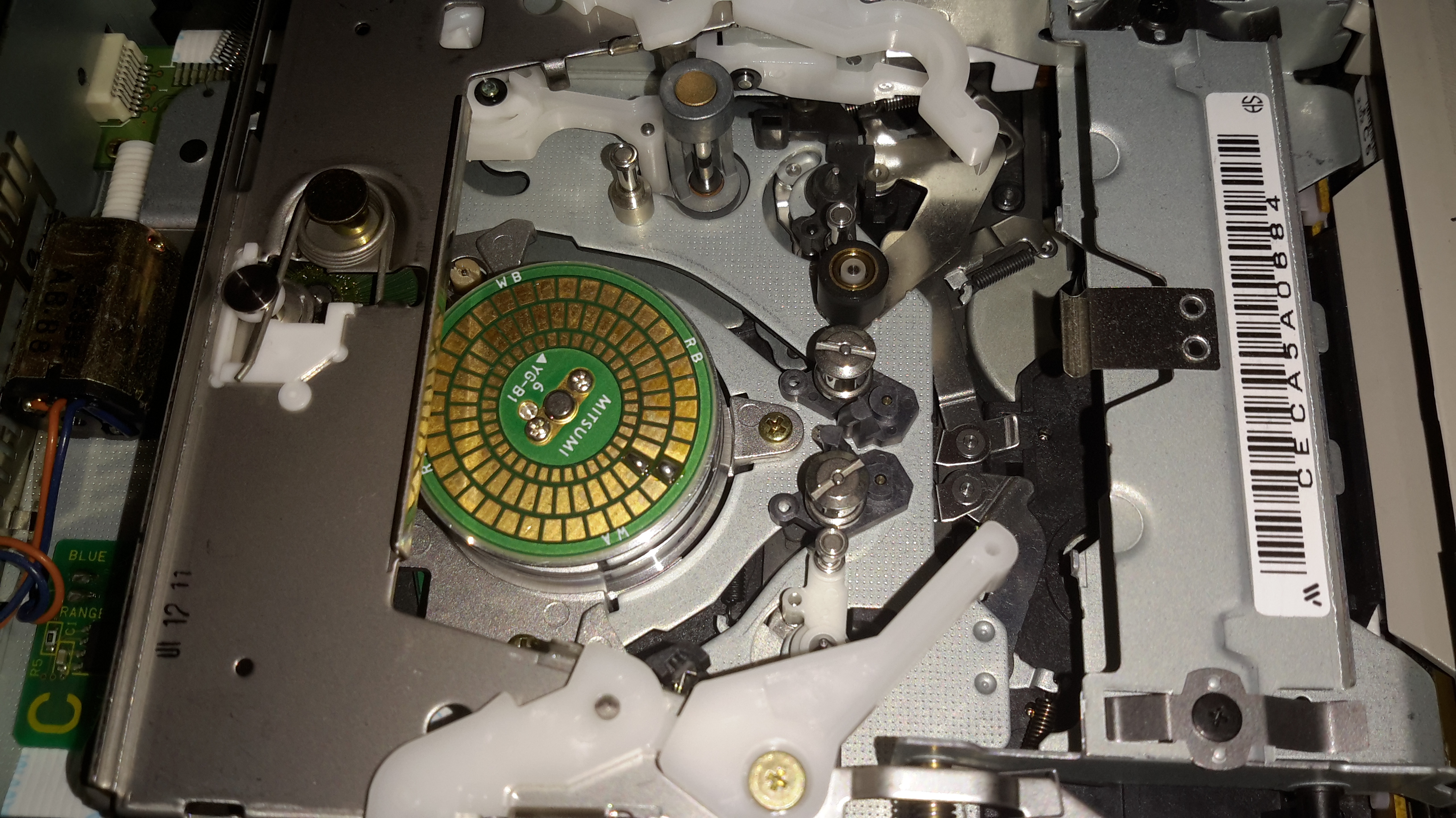
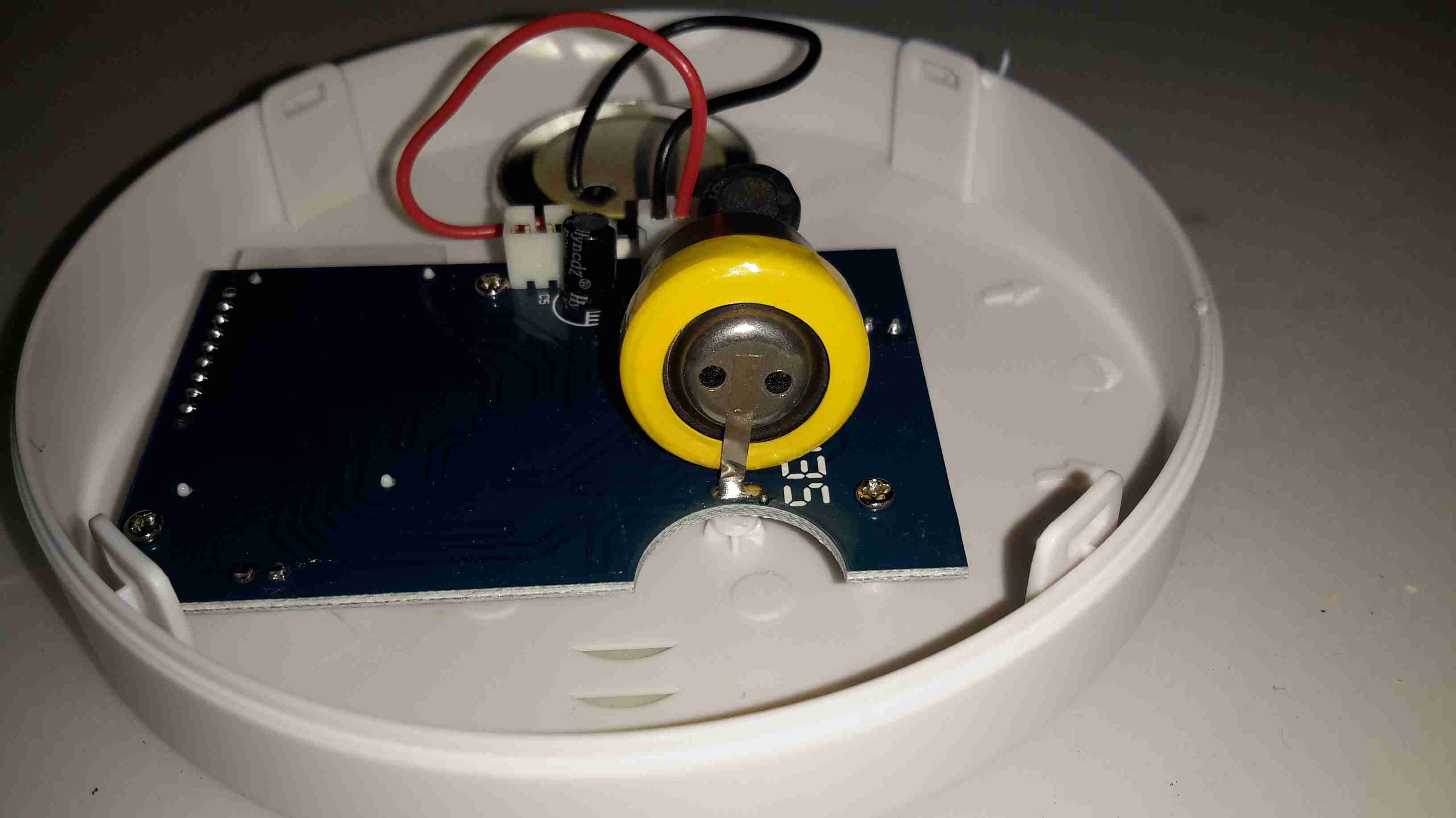
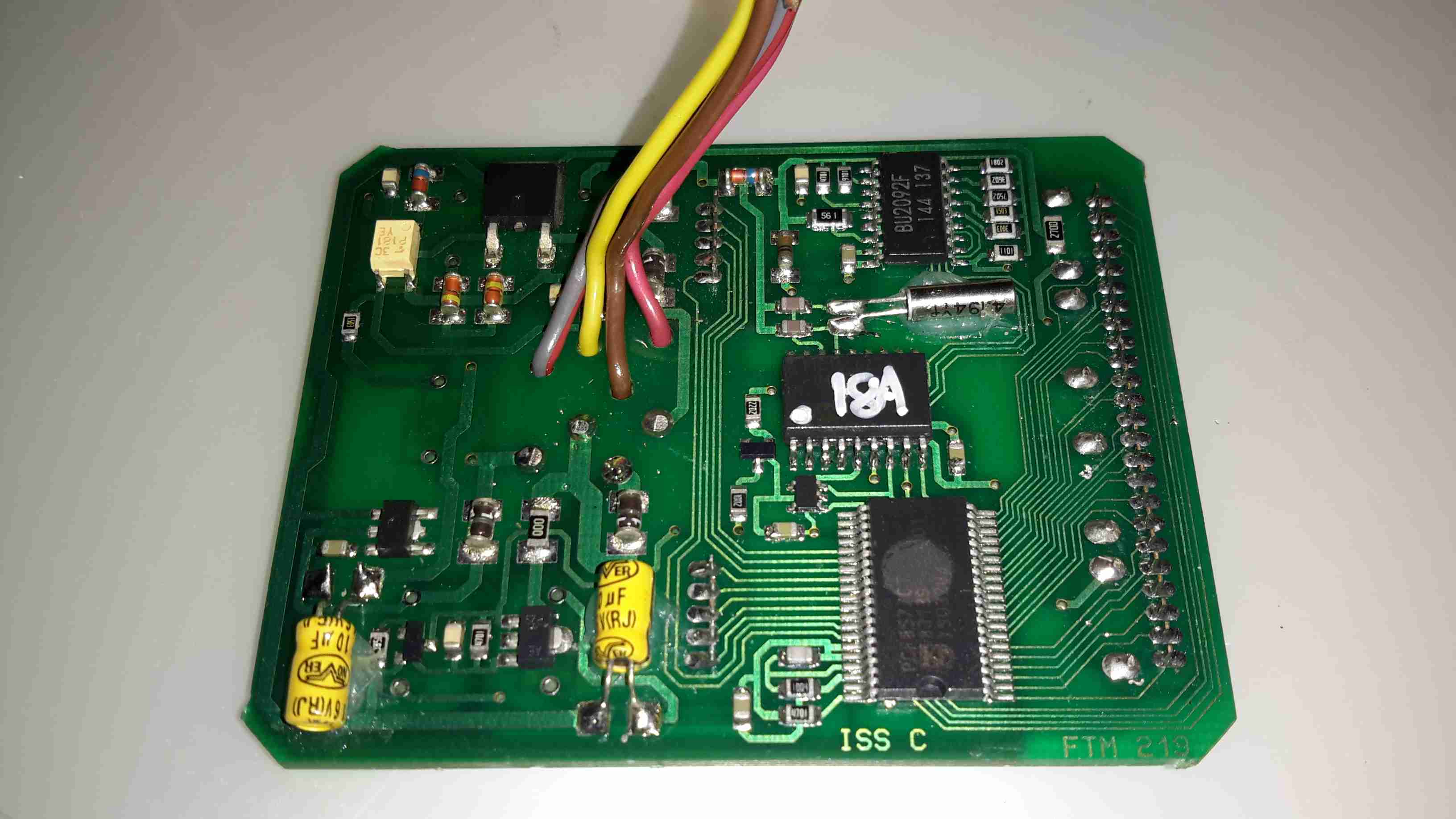
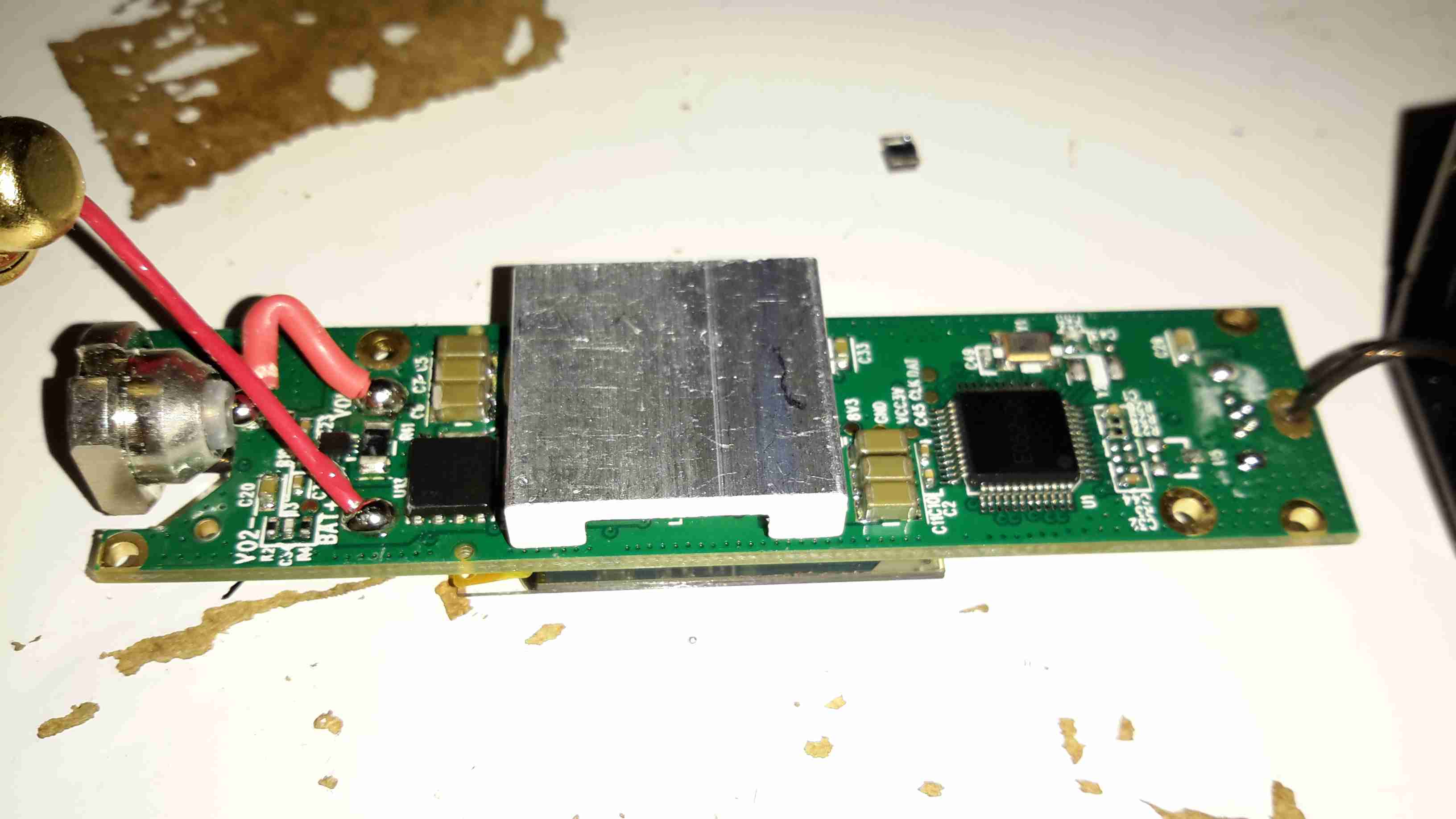
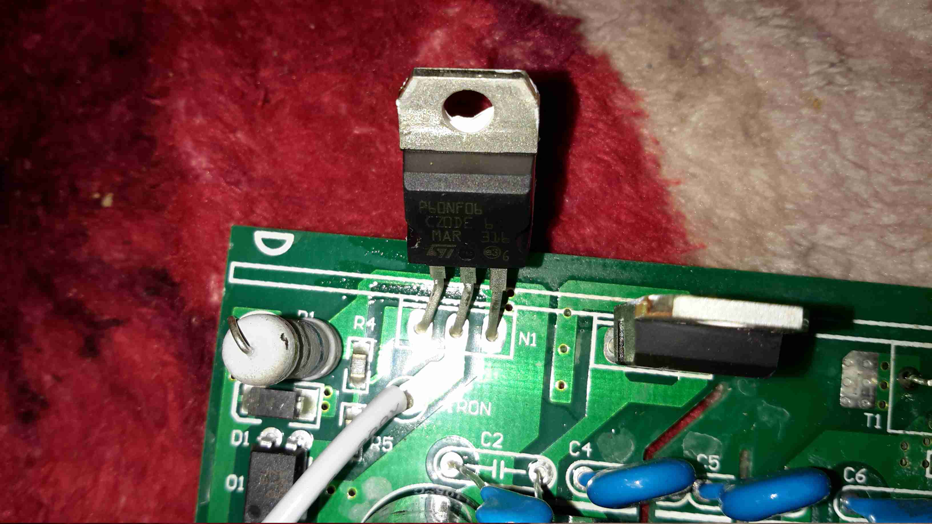
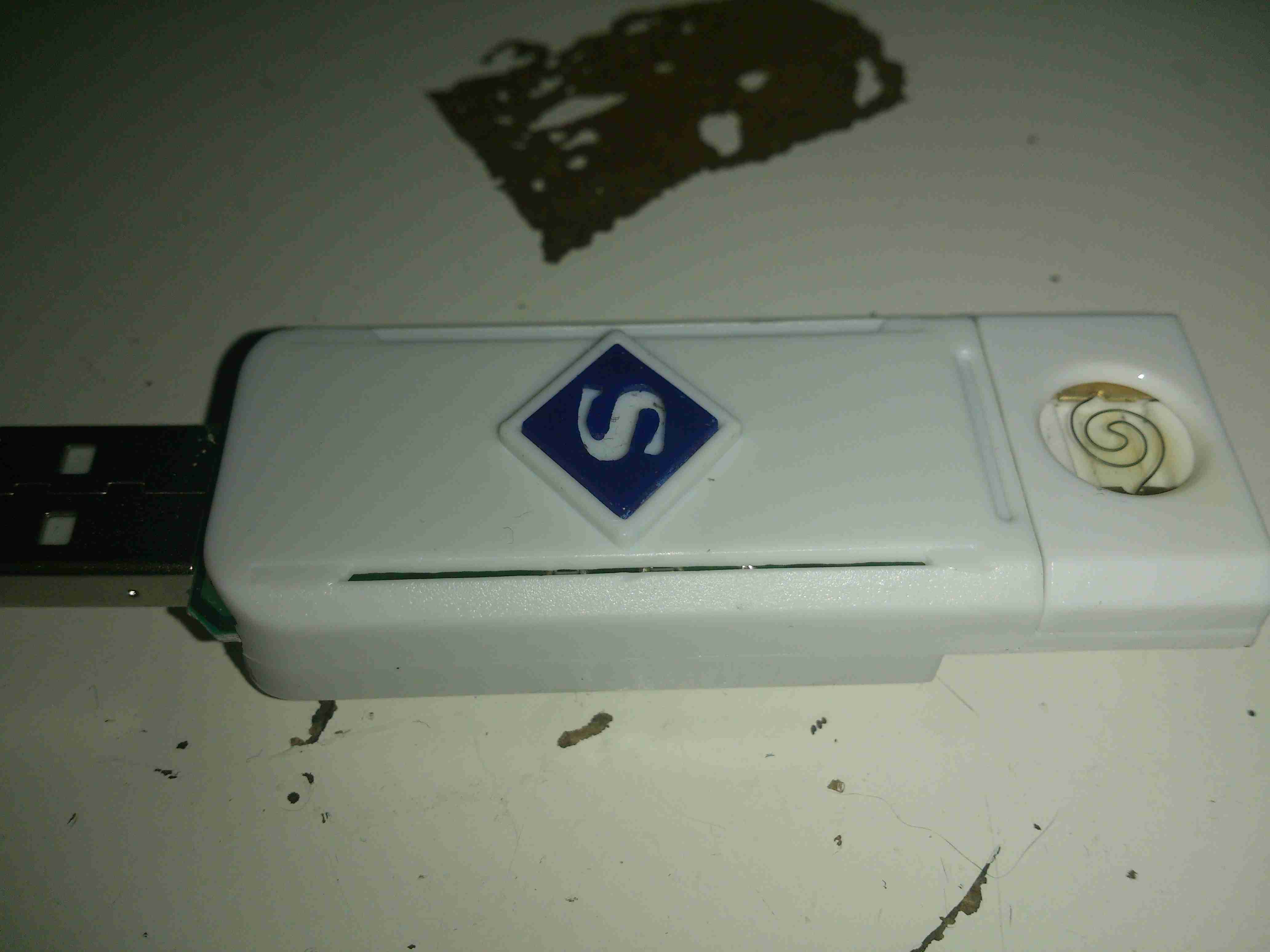
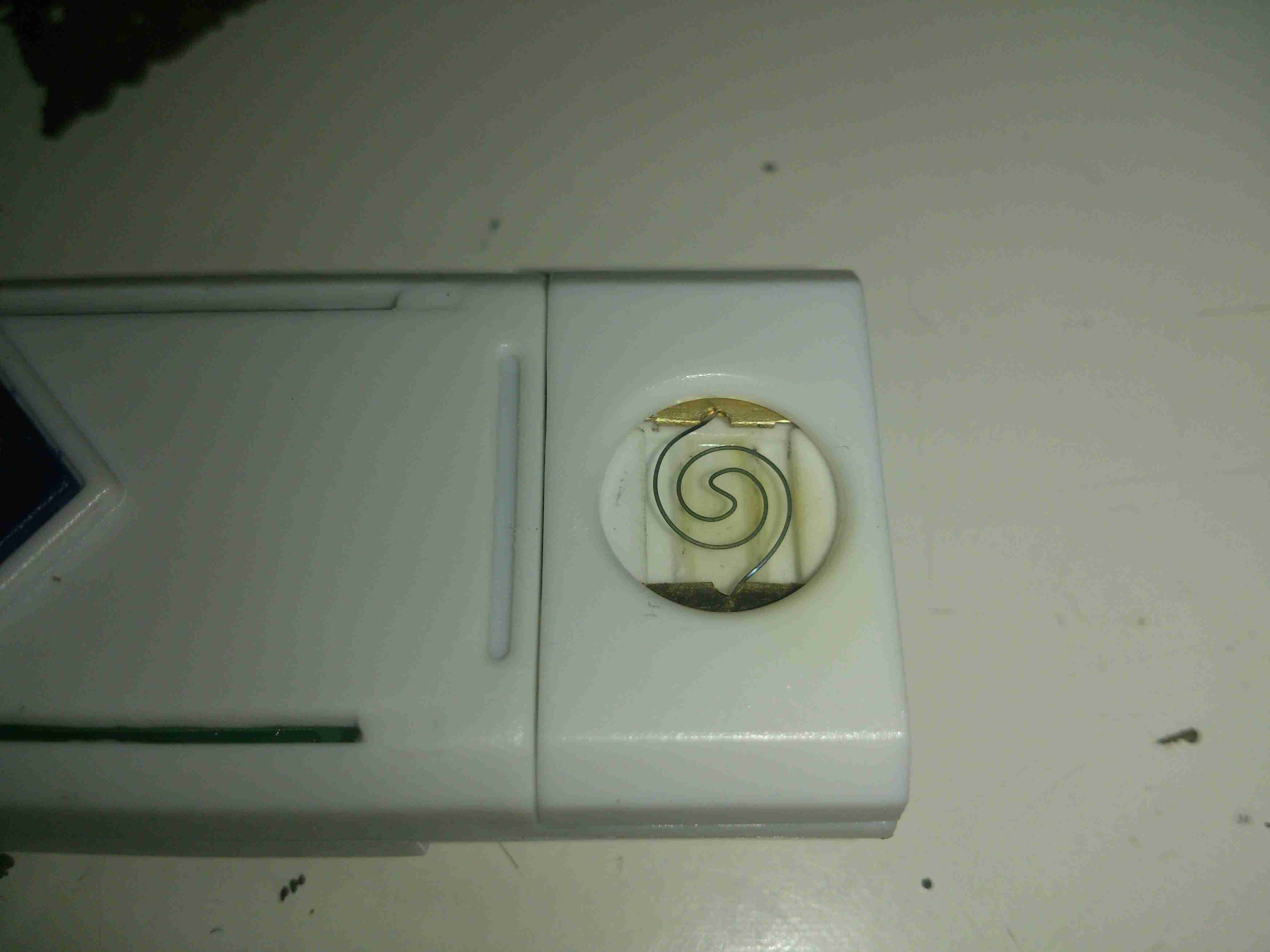
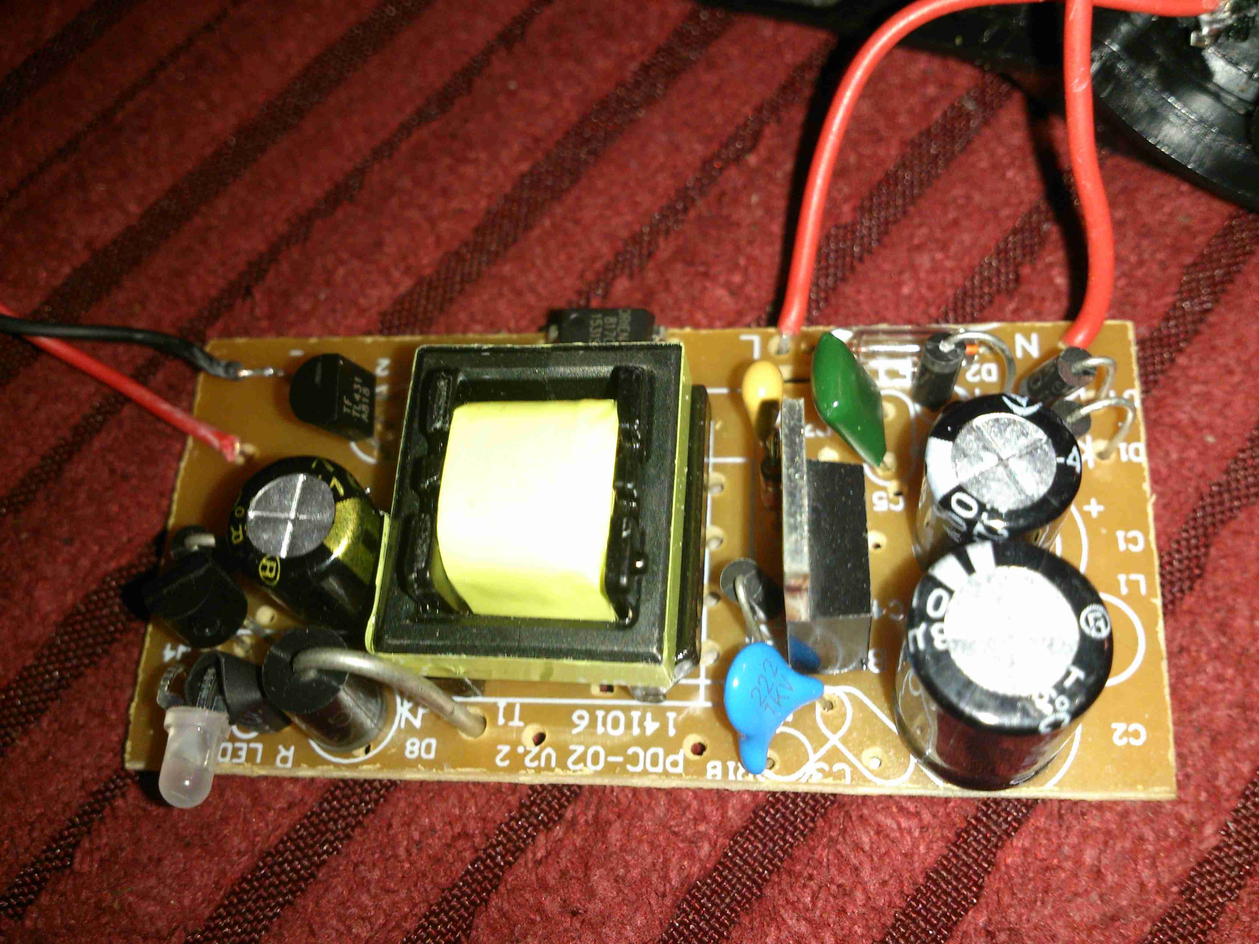
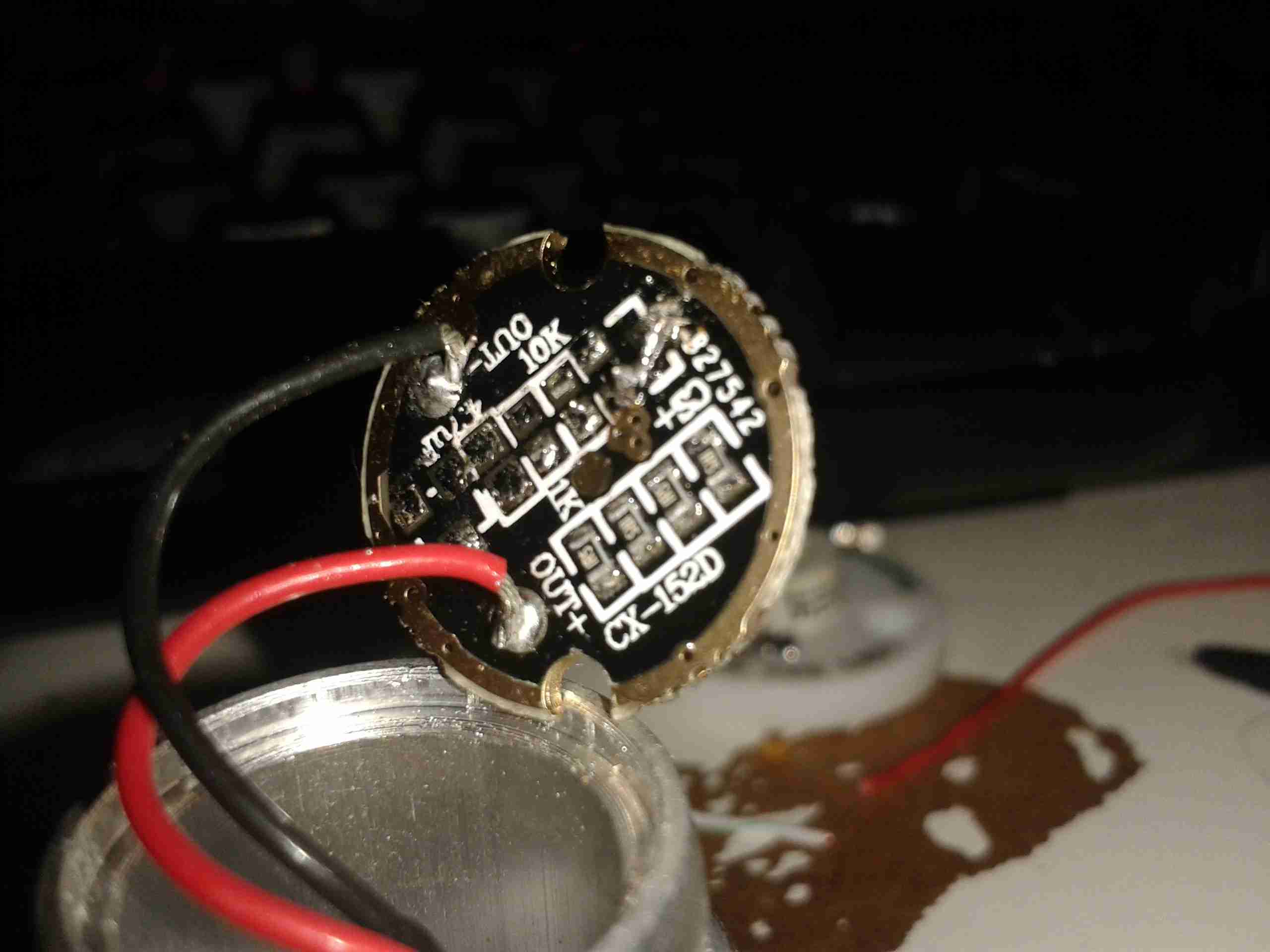
It’s well known that there are two versions of the 701 type controller available for Eberspacher heaters, the version with the blue logo is the official un-restricted model, while the version with the white logo is a version built for BT that restricts the heater to 1 hour runtime & has no diagnostics built in.
As these devices are microcontroller driven, I assumed that the hardware would be the same, only the code running in the micro being the bit that Eberspacher changed. This option would certainly have been the lowest cost.
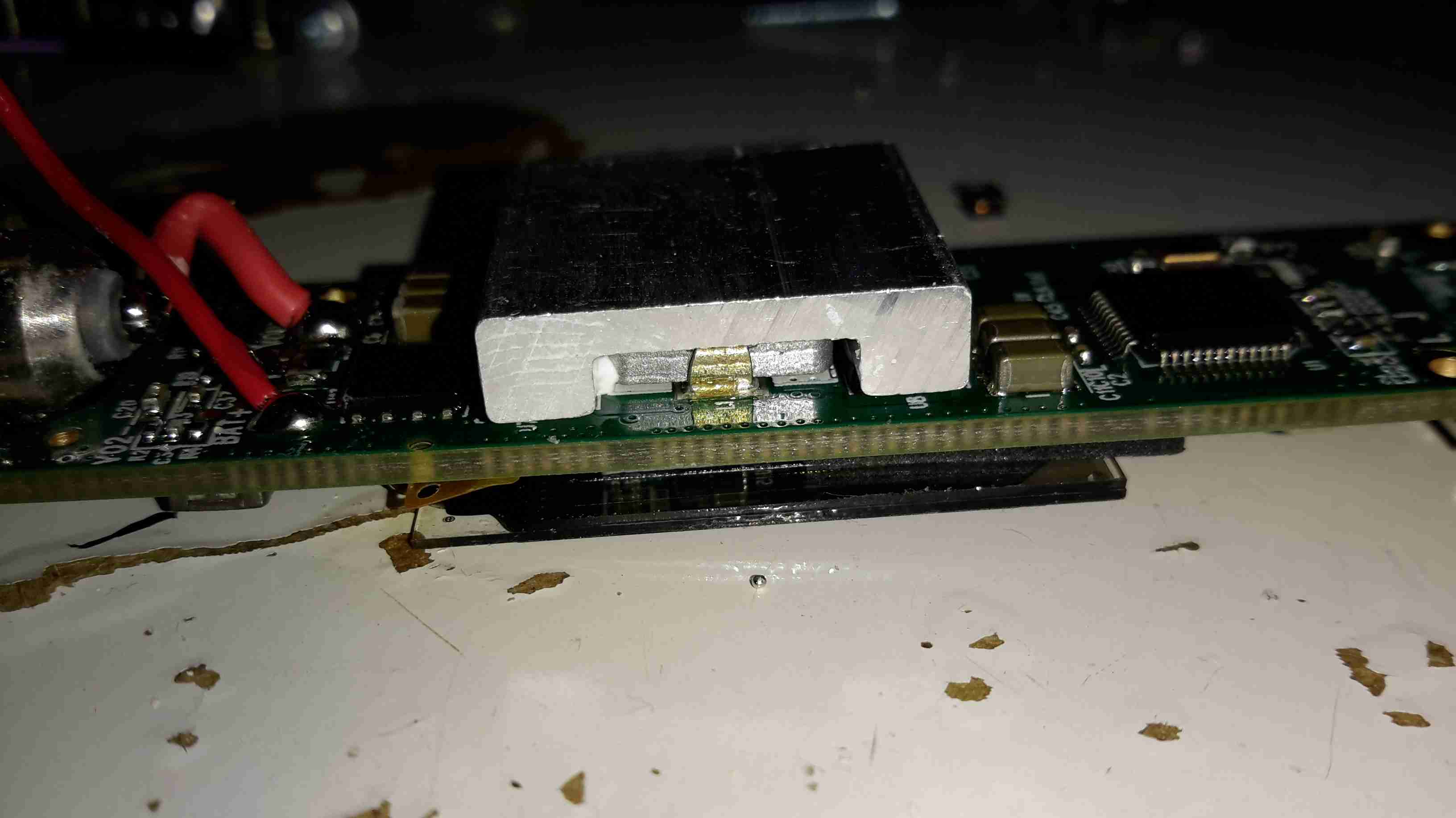
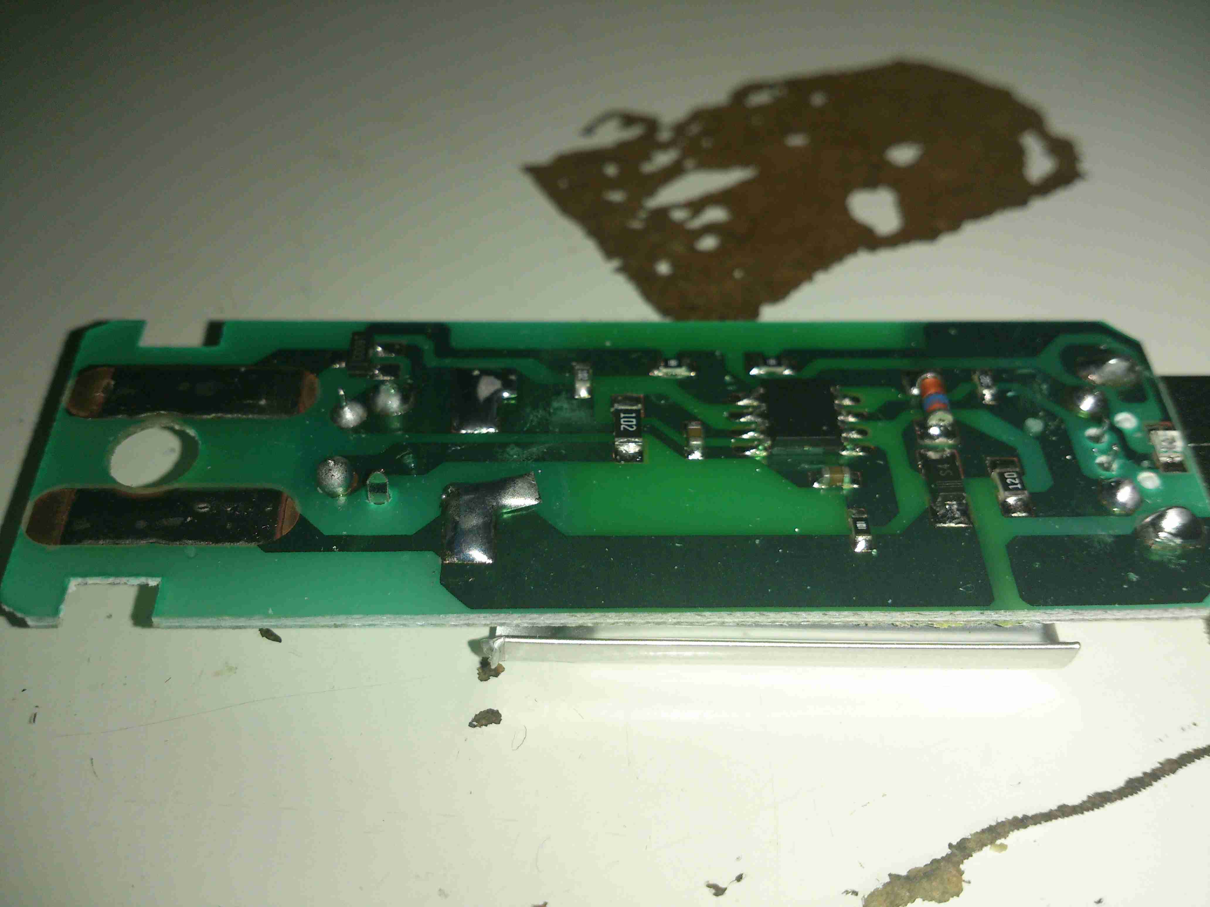
Controller PCB Rear
Here’s the PCB removed from the plastic housing. There are definitely some differences that I can tell. As the un-restricted version has an extra wire for the diagnostic serial interface, and this board has no unpopulated parts, the PCB is definitely a different version.
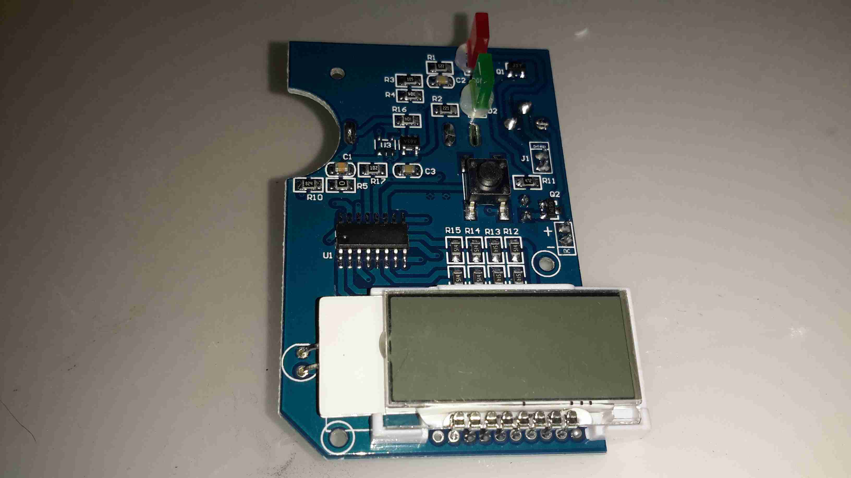
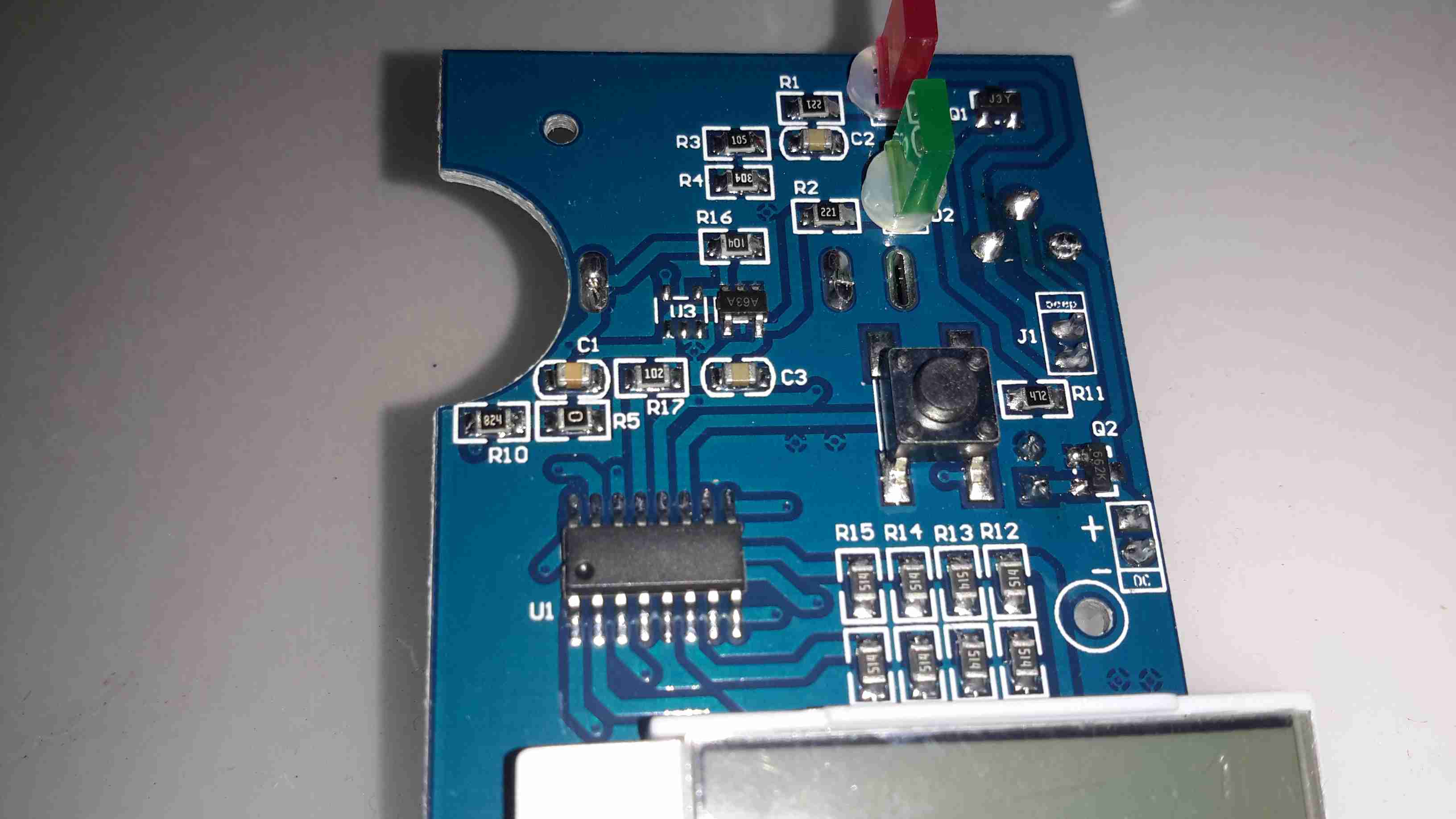
In the centre is a Microchip PIC16C622 microcontroller, the OTP version in this case for cost reductions. (I may try reading the binary from this chip in the future, chances are it’s code protected though).
Below the micro is an NXP PCF8577C 32-segment LCD controller, this has an I²C interface to the PIC.
The temperature control function on these heaters is done via applying a resistance to one of the control lines, between 1750Ω-2180Ω, ±80Ω. (Very odd values these, not to mention no standard components can create this range easily, bloody engineers >_<). This is accomplished in hardware with a BU2092F I²C shift register from Rohm, which is connected to a bank of resistors. The microcontroller will switch combinations of these into the circuit to get the range of resistances required.
The rest of the circuit is local power regulation & filtering.
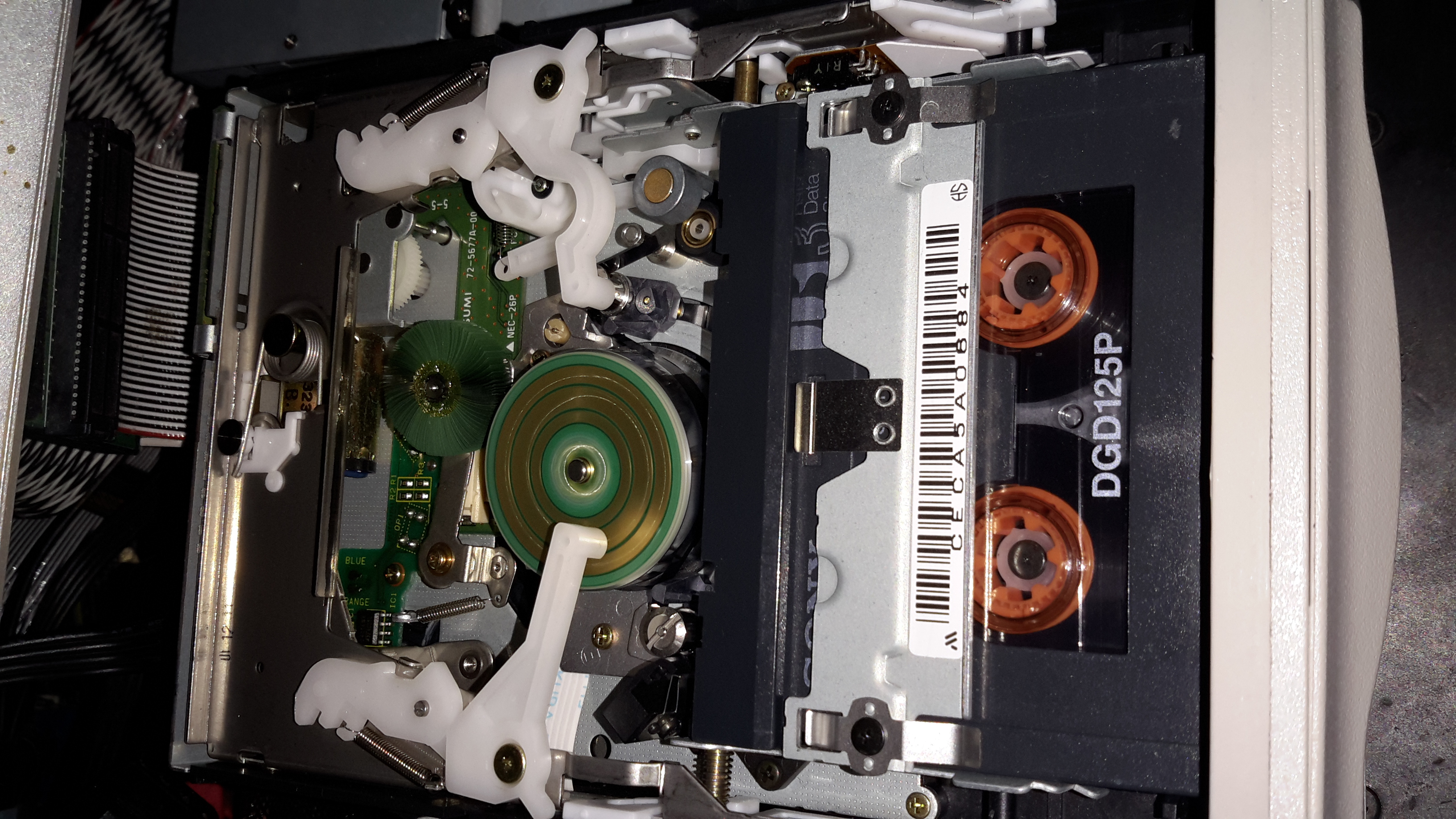
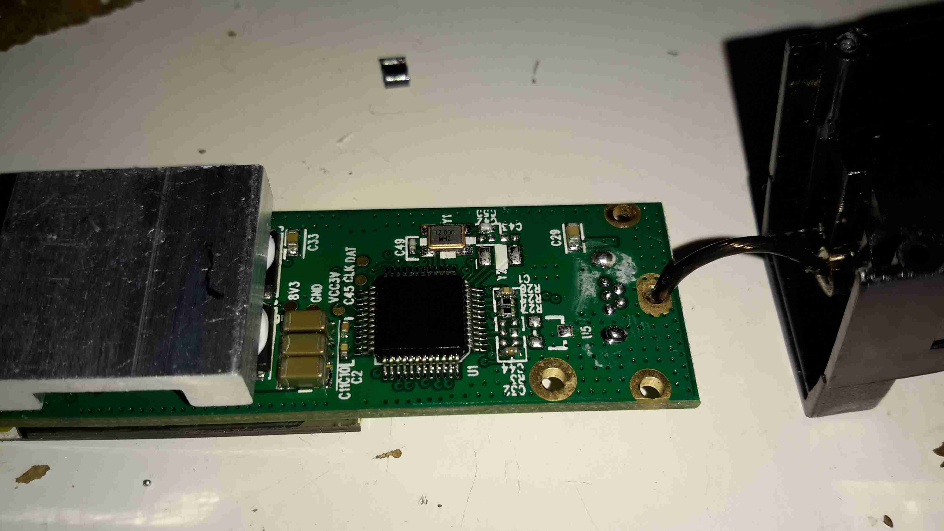
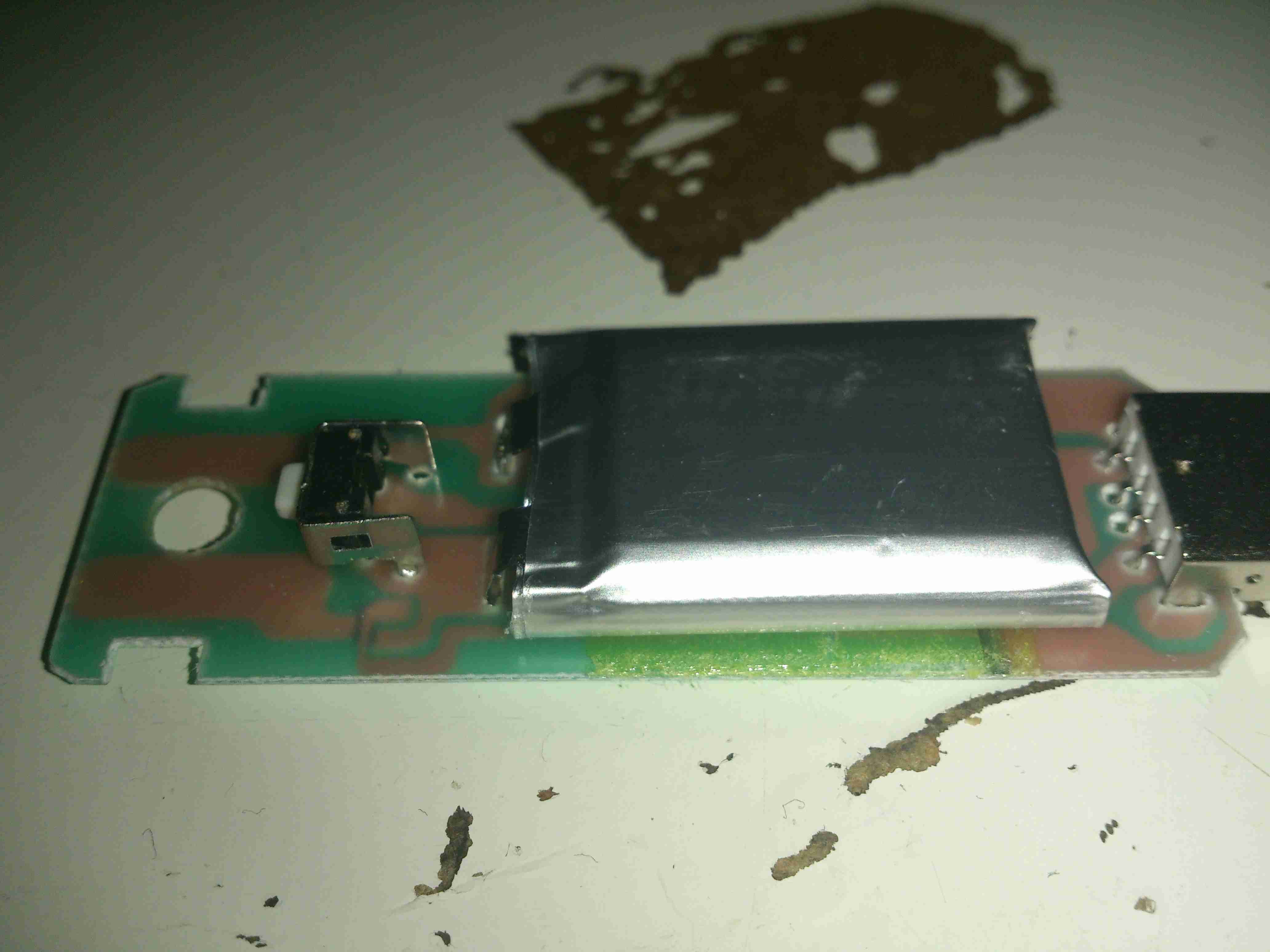
Controller PCB Front
There’s not much on the other side of the PCB, just the LCD itself & the contacts for the buttons.
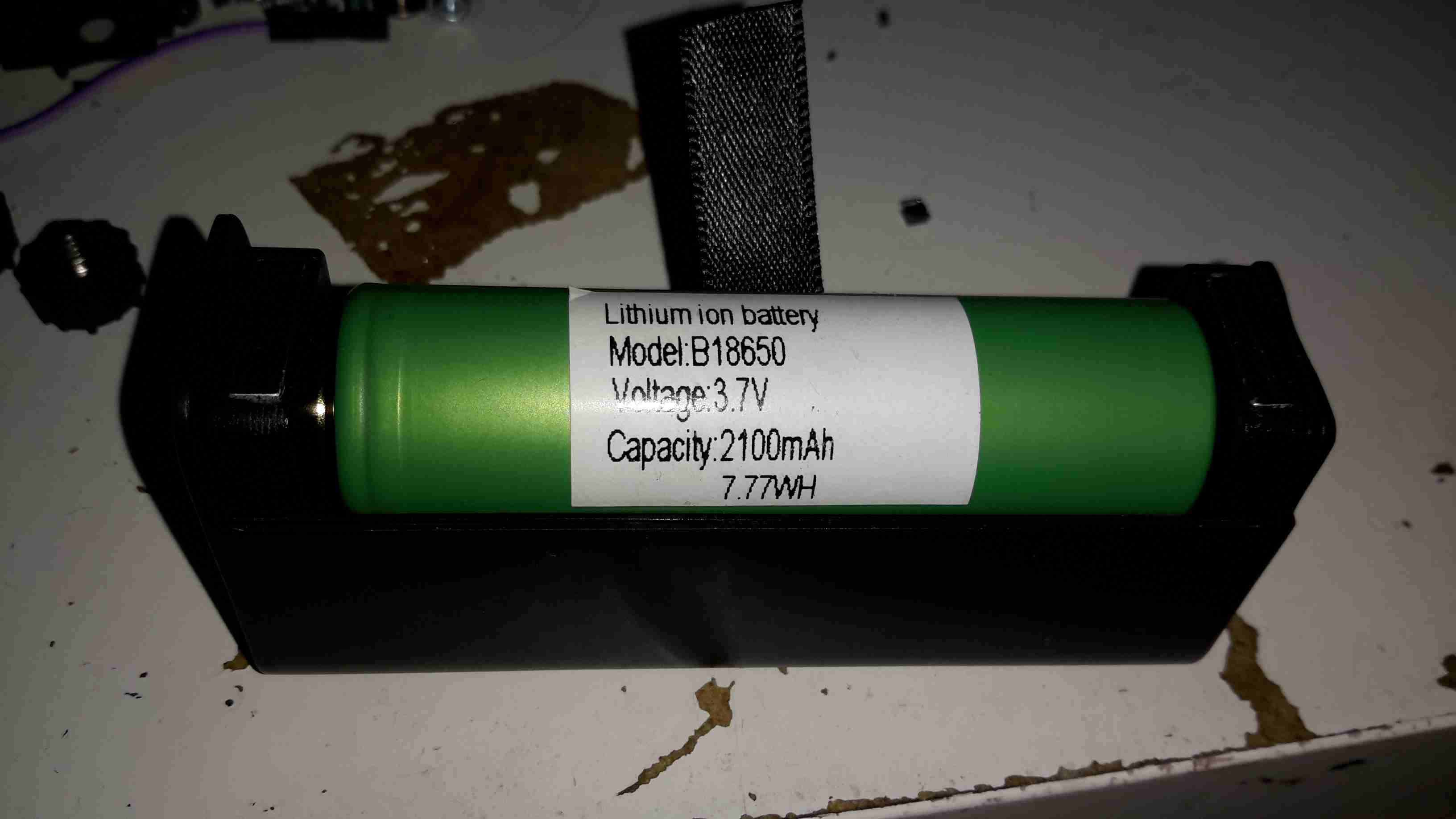
I’ve been a vaper now for many years, after giving up the evil weed that is tobacco. Here’s my latest acquisition in the vaping world, the JoyeTech eVIC 60W. This one is branded by Totally Wicked as the Forza VT60.
18650 Cell
Powered by a single 18650 Li-Ion cell, this one is a Sony VTC4 series, 2100mAh.
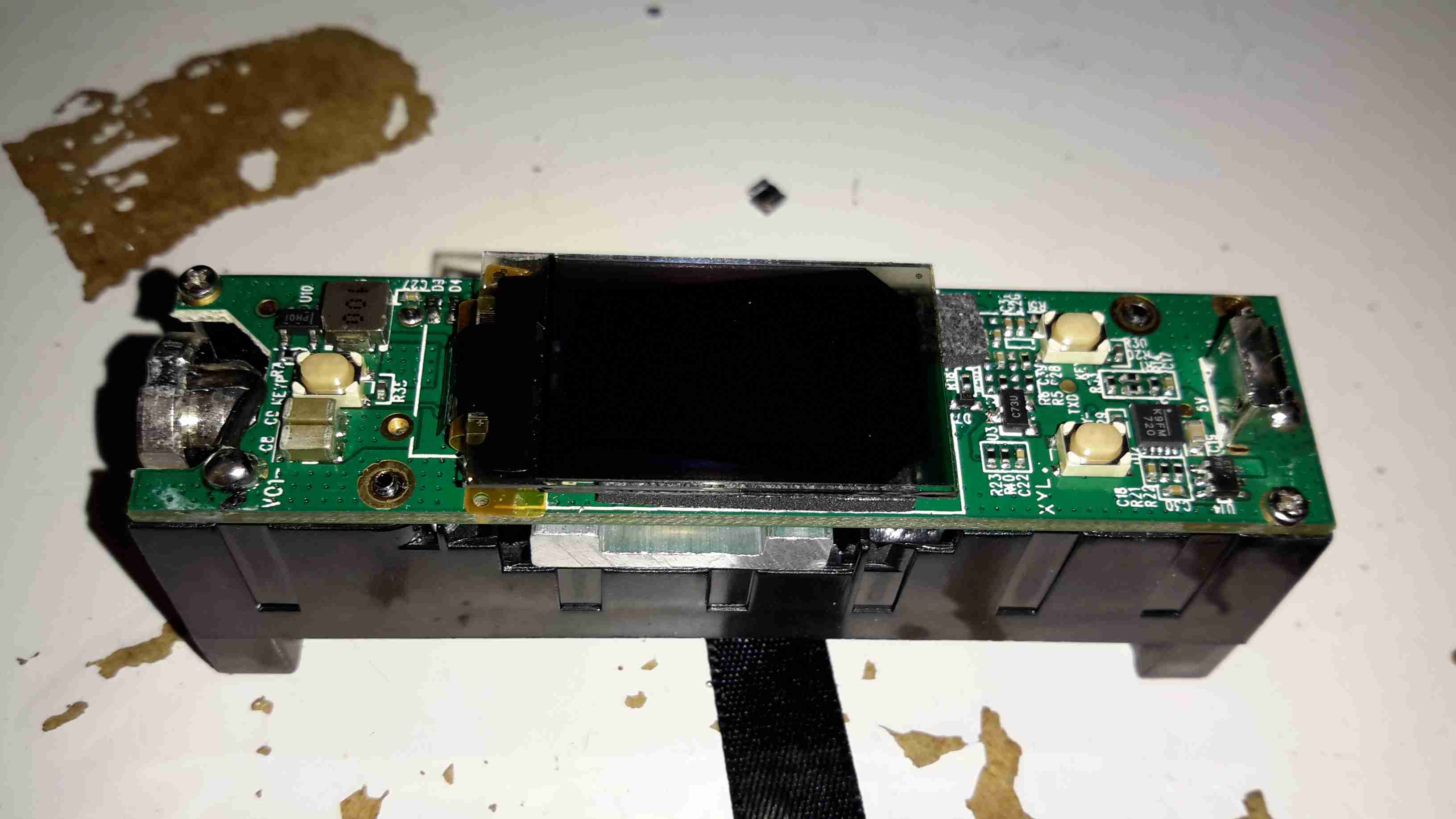
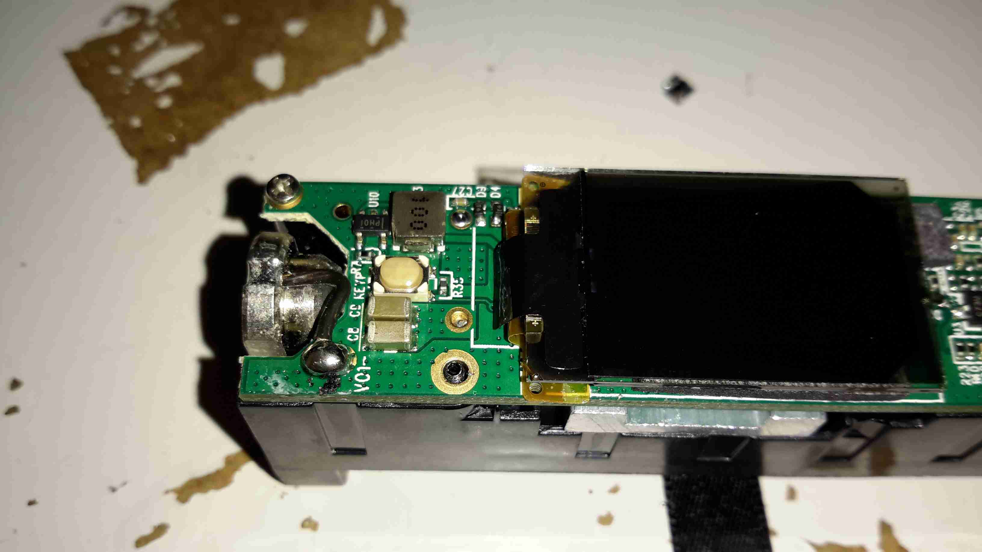
Under the battery a pair of screws hold the electronics in the main cast alloy casing.
OLED Display
After removing the screws, the entire internal assembly comes out of the case, here’s the top of the PCB with the large OLED display in the centre.
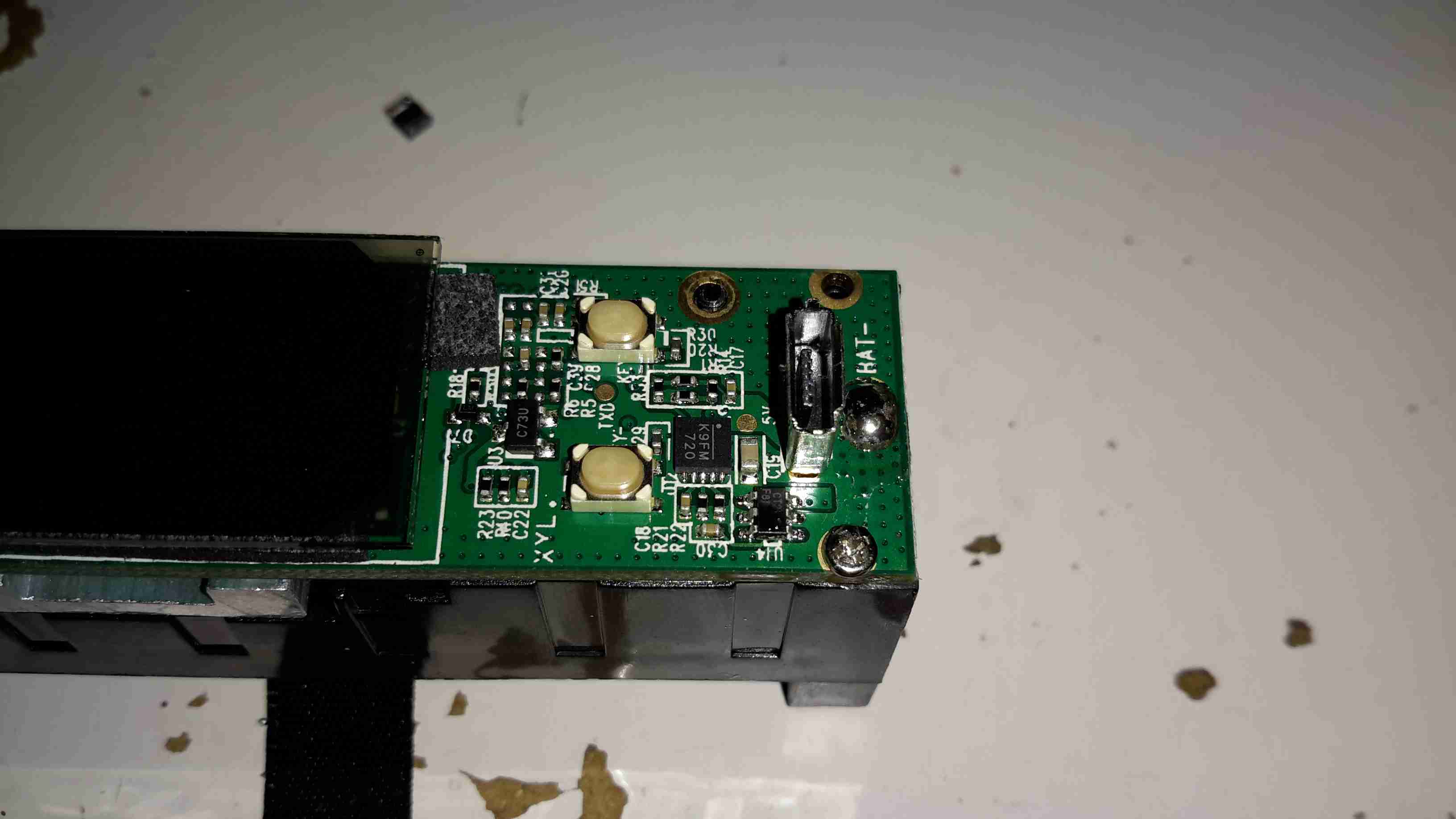
USB Jack
On the right side of the board is the USB jack for charging & firmware updates. The adjustment buttons are also at this end.
Output
On the left side of the board is the main output connector & the fire button. Unlike many eCigs I’ve torn down before, the wiring in this one is very beefy – it has to be to handle the high currents used with some atomizers – up to 10A.
PCB Reverse
Removing the board from the battery holder shows the main power circuitry & MCU. The aluminium heatsink is thermally bonded to the switching MOSFETs, a pair under each end. The switching inductor is under the gap in the centre of the heatsink.
DC-DC Converter
A close up of the heatsink shows the very slim inductor under the heatsink.
Microcontroller
The main MCU in this unit has a very strange part number, which I’ve been unable to find information on, but it’s probably 8081 based.
Inkeeping with everything else in my shack being low voltage operated, I had planned from the outset to convert the desoldering station to 12v operation. It turns out this has been the easiest tool to convert in my shack so far.
PSU Outputs
The factory SMPS is a fairly straightforward 18v 12A unit, with only a single small oddity: the desoldering gun’s heating element is controlled from inside the supply.
Iron MOSFET
Next to the output rectifier on the heatsink is a large MOSFET, in this case a STP60NF06 from ST Micro. This is a fairly beefy FET at 60v & 60A capacity, RDS On of <0.016Ω.
This is driven via an opto-isolator from the main logic board. I’ve not yet looked at the waveform on the scope, but I suspect this is also being PWM’d to control temperature better when close to the set point.
Iron Element Controller
Rather than fire up the soldering iron & build a new element controller circuit (Lazy Mode™), I opted to take a saw to the original power supply. I cut the DC output section of the PCB off the rest of the supply & attached this piece back to the frame of the base unit. I also added a small heatsink to the MOSFET to make sure it stays cool.
12v Power Supply
Since the fan & vacuum pump are both already 12v rated, those are connected directly to the DC input socket, that I’ve installed in place of the original IEC mains socket. The 18v for the heating element is generated by a 10A DC-DC converter, again from eBay.
Oddly, the iron itself is rated at 24v 80W, but the factory supply is only rated to 18v. I’m not sure why they’ve derated the system, but as the station already draws up to 10A from a 13.8v supply, increasing the voltage any further would start giving my DC supplies a problem, so it can stay at 18v for now.
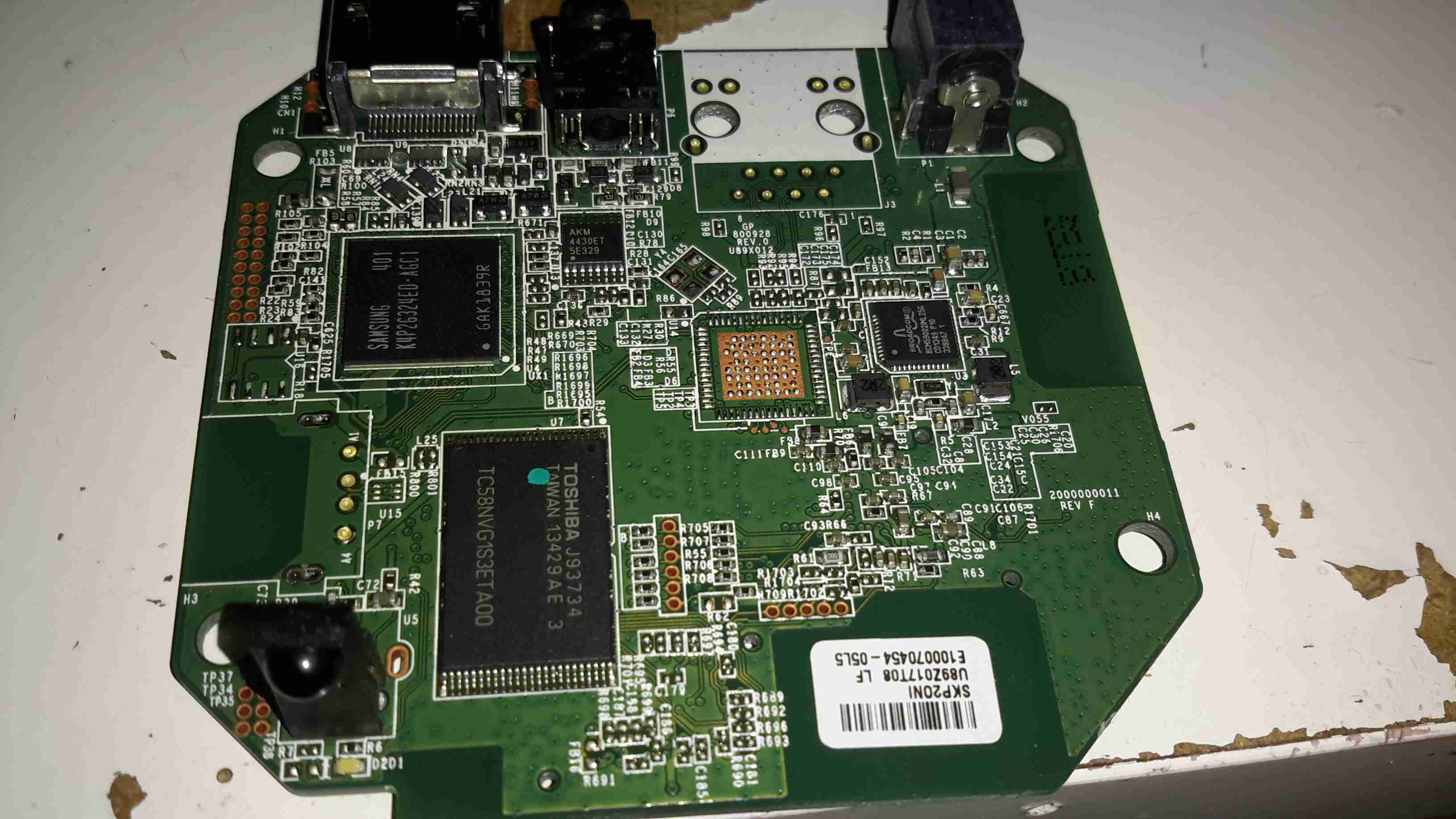
Here’s another retired piece of tech that we used to route media from the NAS to the main TV. It was retired since it’s inability to support XBMC/Kodi & having some crashing issues.
Main PCB
After attacking the case with the screwdriver (Torx in this case), the main board comes out. The CPU in this looks *very* familiar, being a PoP device. There are unpopulated places for an ethernet interface & USB port here.
Flash & CPU
After a little digging is turns out the CPU in this device is a BCM2835, with 256MB of RAM stacked on top. It’s a Raspberry Pi! Even the unpopulated part for Ethernet is the same SMSC LAN9512!
There’s 32MB of Flash for the software below the CPU.
On the far right of the board is a Broadcom BCM59002IML Mobile Power Management IC.
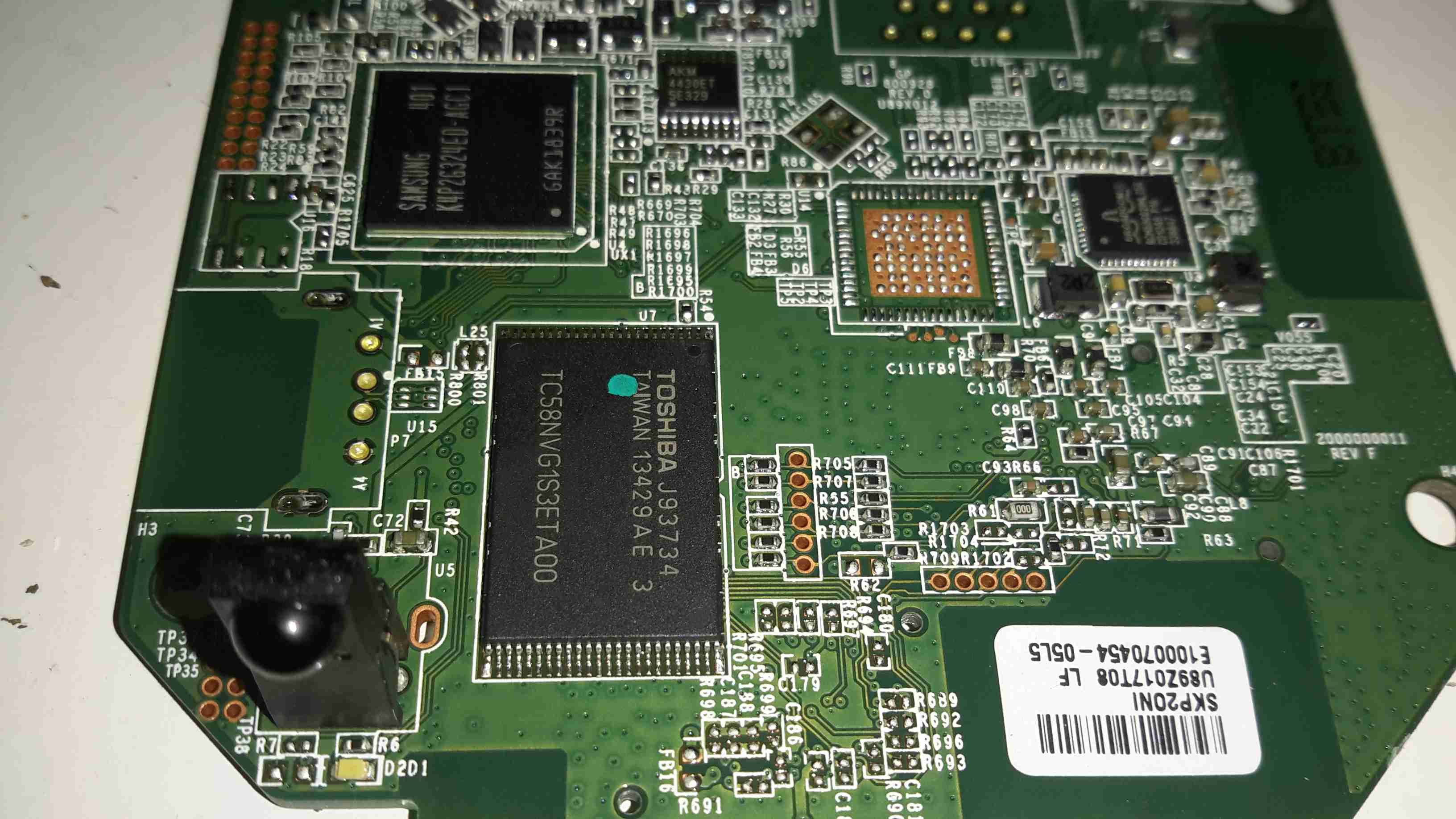
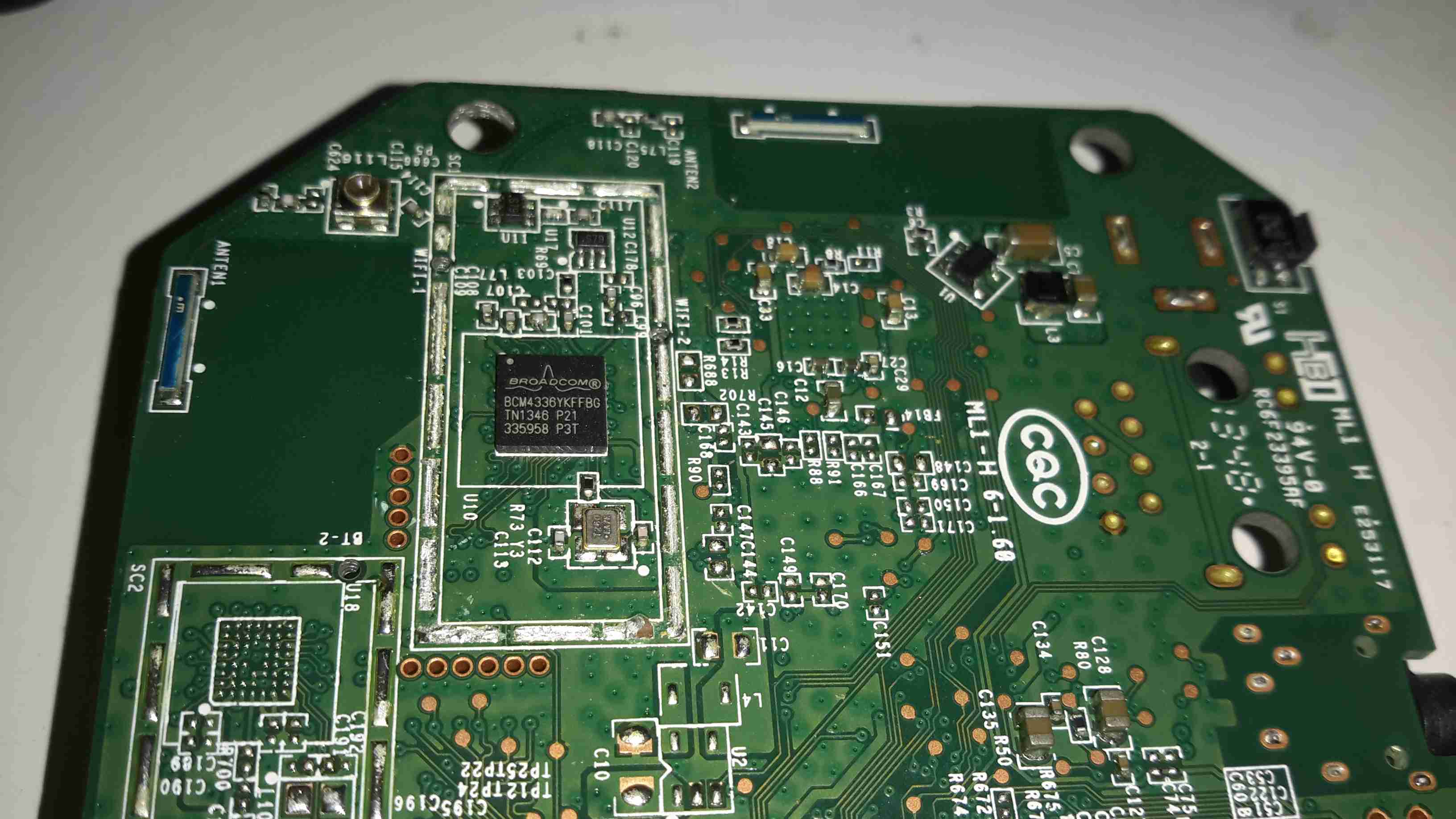
WiFi Chipset
On the bottom of the PCB is the WiFi chipset, a Broadcom BCM4336, this most likely communicates with the CPU via SDIO. There’s also a section below for a Bluetooth chipset.
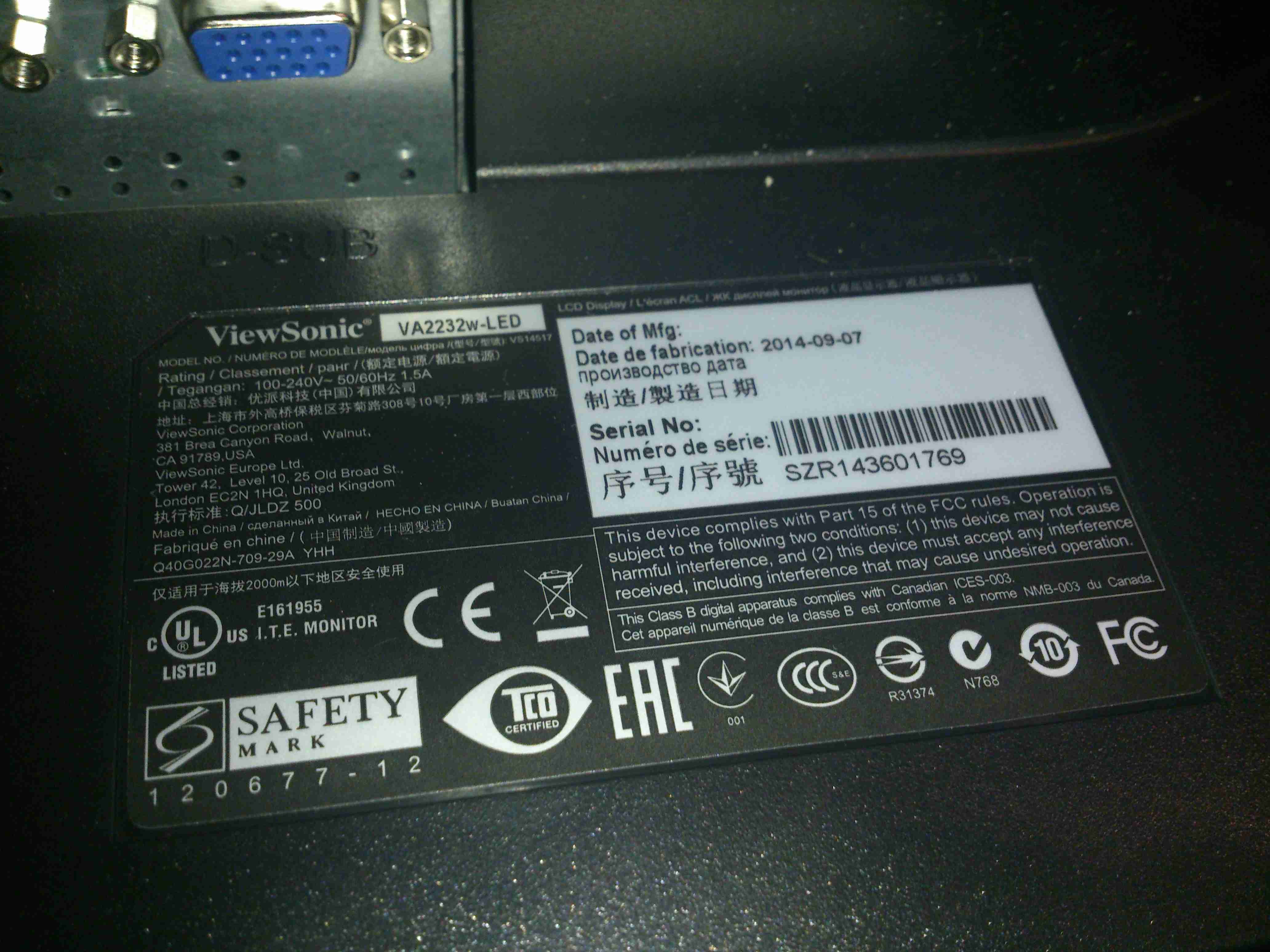
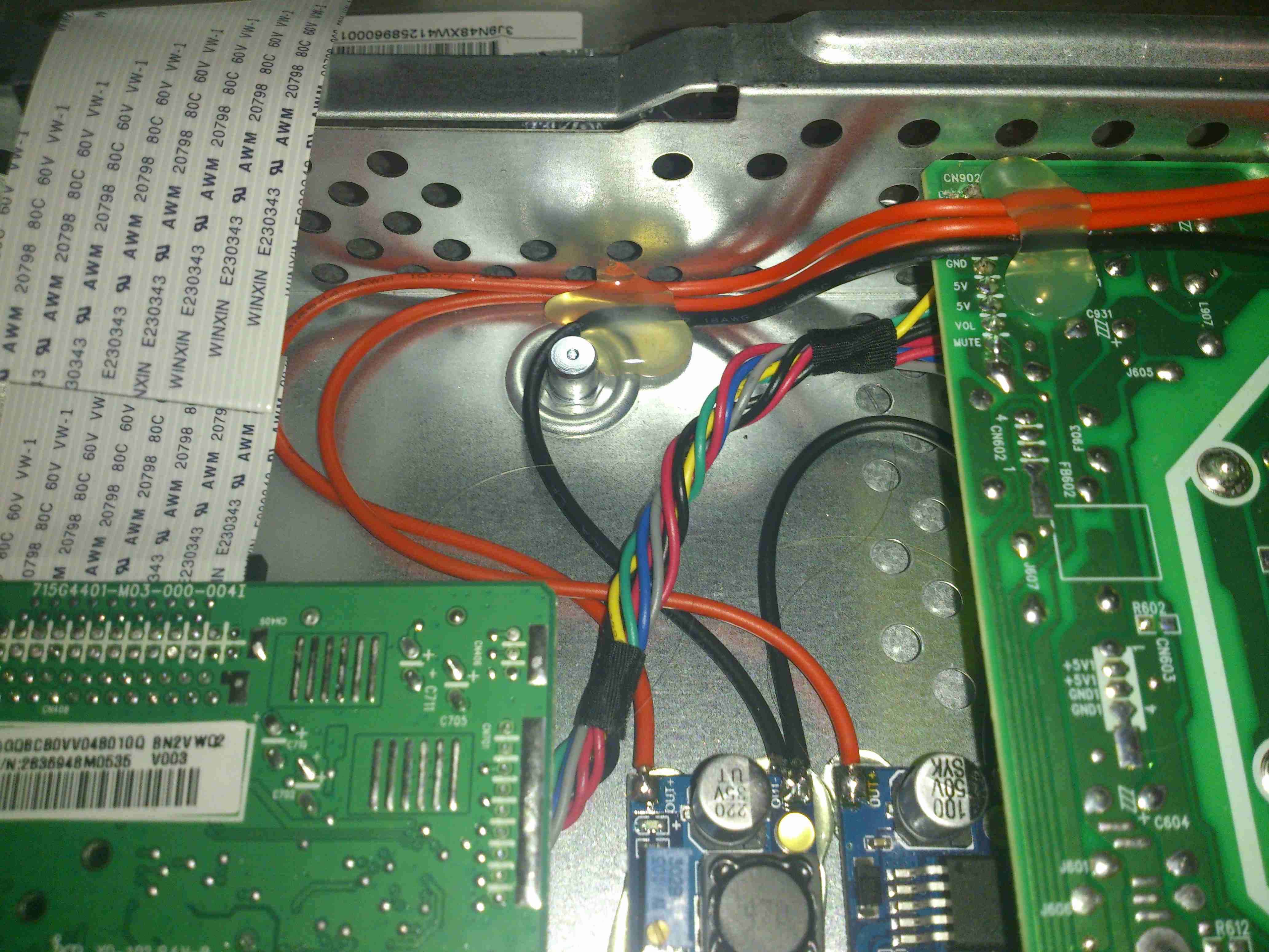
On the quest to get things on board replaced that are heavy users of power, the monitor in the main cabin was next. The original CCFL-backlit monitor was very heavy on 12v power, at 5A. This meant falling asleep watching TV would result in severely flattened batteries.
Replacement with a suitable LED-backlit monitor was definitely required. The cheapest on eBay was a ViewSonic VA2232W-LED, so I took to work converting it from 240v to 12v operation.
Back Cover Removed
There are no screws holding these monitors together, so a spudger & frequent swearing got the back off. The shield holding the circuitry is also not screwed down, only attached to the back of the LCD panel with aluminium shielding tape.
Power PCB Trackside
Once the tape has been cut, the main power board is accessible. The large IC on the left is the main backlight LED driver.
In this case the monitor requires a pair of rails from the supply, 18.5v for the backlight circuitry & 5v for the logic.
DC-DC Regulators
A pair of DC-DC converters has been fitted in the small space between the power & control boards.
PCB Connection Points
To save me some work & keep maximum compatibility, I’ve not modified the existing supply, just attached the new DC-DC converter outputs onto the corresponding outputs of the factory PSU. The 12v input leads are routed out of the same gap as the mains IEC connector, with some hot glue over the mains input solder points to provide some more insulation.
Wiring Tidied
The wiring is tidied up with hot glue so the back cover will go back on.
With a recent order from a Chinese seller on eBay, this little gadget was included in the package as a freebie:
Electronic Lighter
I’ve not smoked for a long time, so I’m not too sure what use I’m going to find for this device, but it’s an electronic lighter!
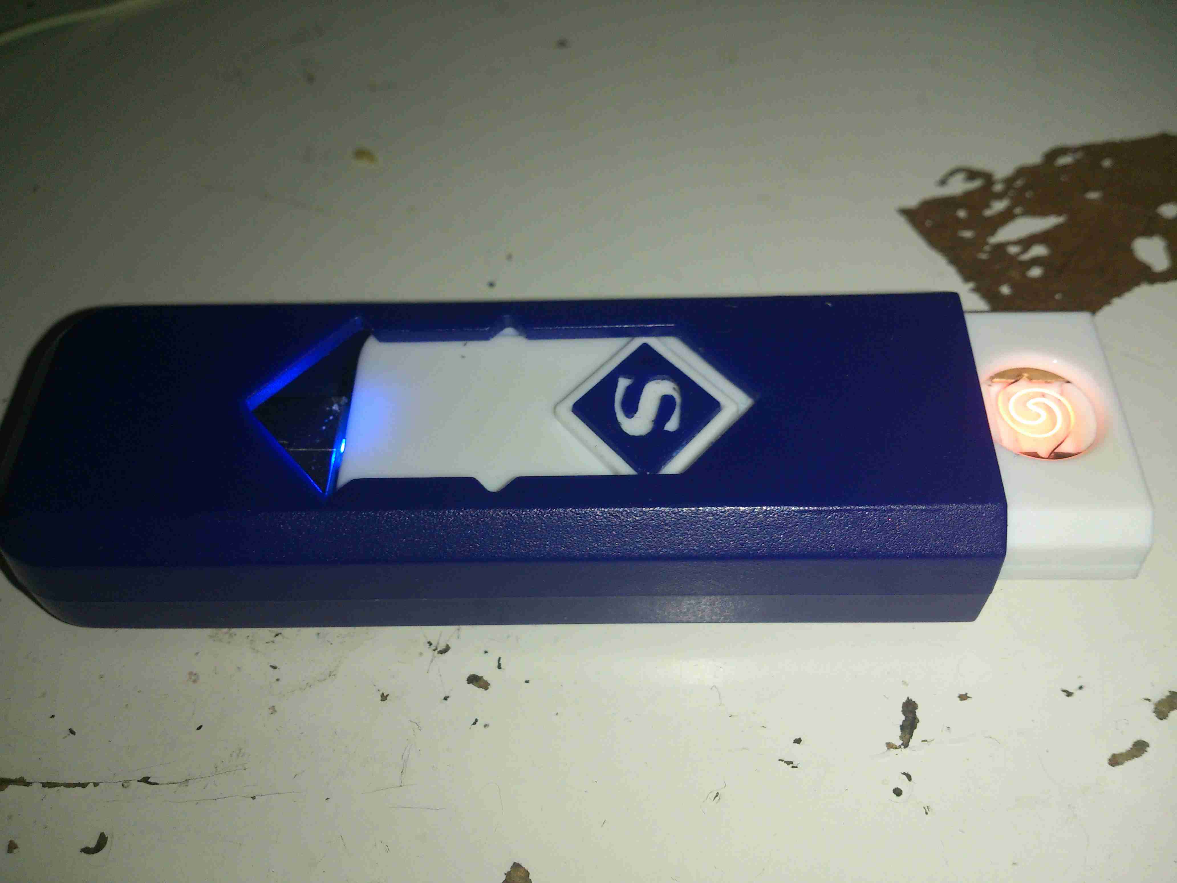
Pyromaniac Mode
Pushing the slider forward reveals a red-hot heater, mounted in the plastic (!) frame.
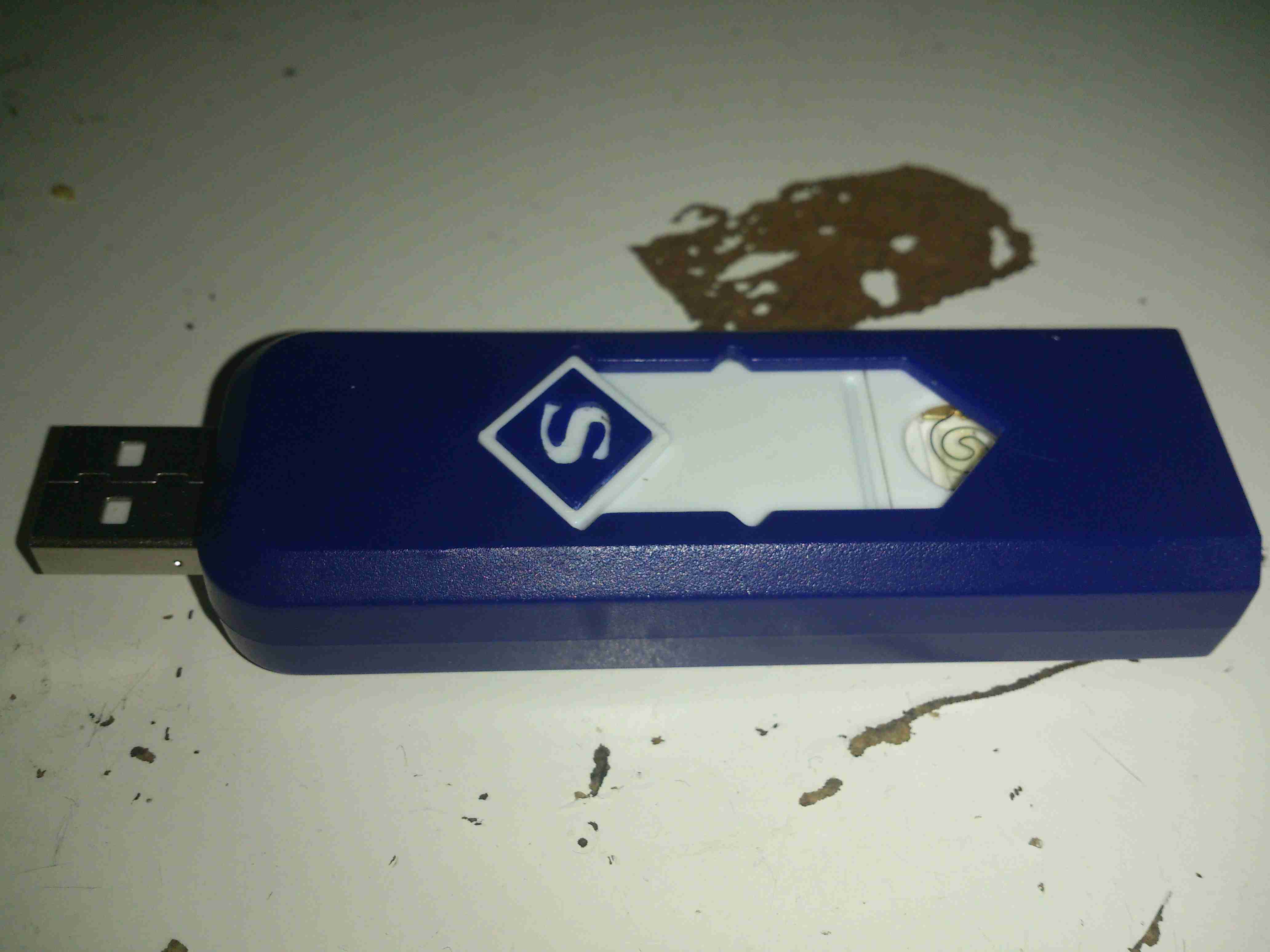
Charging Mode
Pushing the other way reveals a USB port to charge the internal battery.
Core Removed
A couple of screws releases the end cap from the cover & the entire core unit slides out. Like all Chinese toys it’s made of the cheapest plastic imaginable, not such a good thing when heat is involved.
Heating Element
The element itself is a simple coil of Nichrome wire, crimped to a pair of brass terminals. The base the heater & it’s terminals are mounted to is actually ceramic – the surround though that this ceramic pill clips into is just the same cheap plastic. Luckily, the element only remains on for a few seconds on each button push, there’s no way to keep it on & start an in-pocket fire, as far as I can see.
Main PCB
The main PCB clips out of the back of the core frame, the large pair of tinned pads on the left connect to the heater, the control IC has no numbering of any kind, but considering the behaviour of the device it’s most likely a standard eCig control IC.
LiPo Cell
The other side of the board has the USB port on the right, the Lithium Polymer cell in the centre, and the power button on the left. The cell itself also has no marking, but I’m guessing a couple hundred mAh from the physical size.
Compressed air is a rather useful power source, especially when all maintenance is done by the on board crew instead of by boatyards.
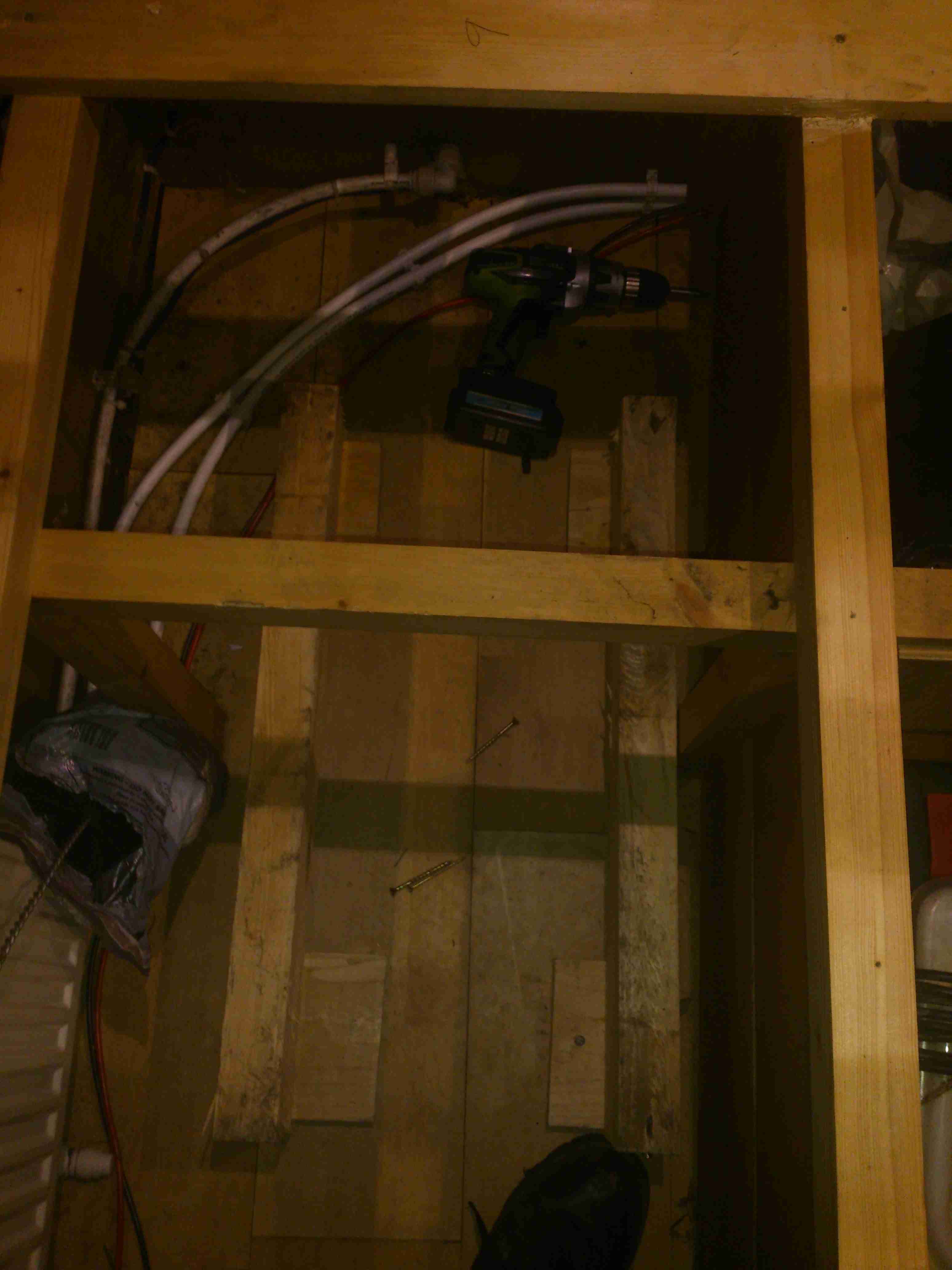
Screwfix had a good deal on a 50L 3.5CFM air compressor, to save space this has been permanently mounted in a free space & air will be piped to where it is needed from a central point.
Because of the total height of the machine, the compressor itself has been unbolted from the tank, a copper line connecting the two back together at a larger distance.
Bearers
In one of the very few free spaces available, under a bunk. A pair of timbers has been screwed to the floor to support the tank.
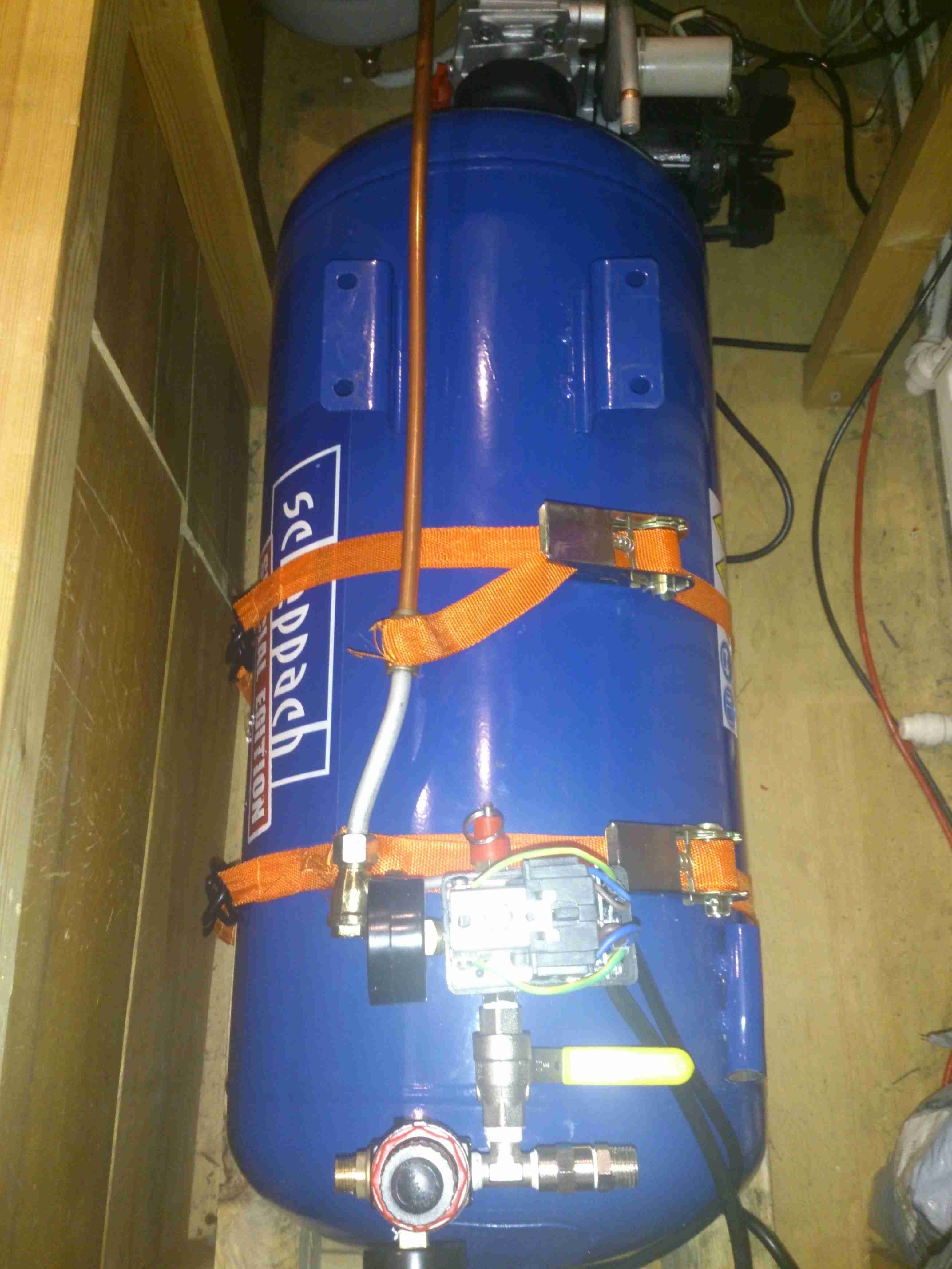
Tank Installed
The tank is strapped to the wooden supports with a pair of ratchet straps, the compressor itself can be seen just behind the tank. The copper line on the top of the tank is going back to be connected to the compressor outlet.
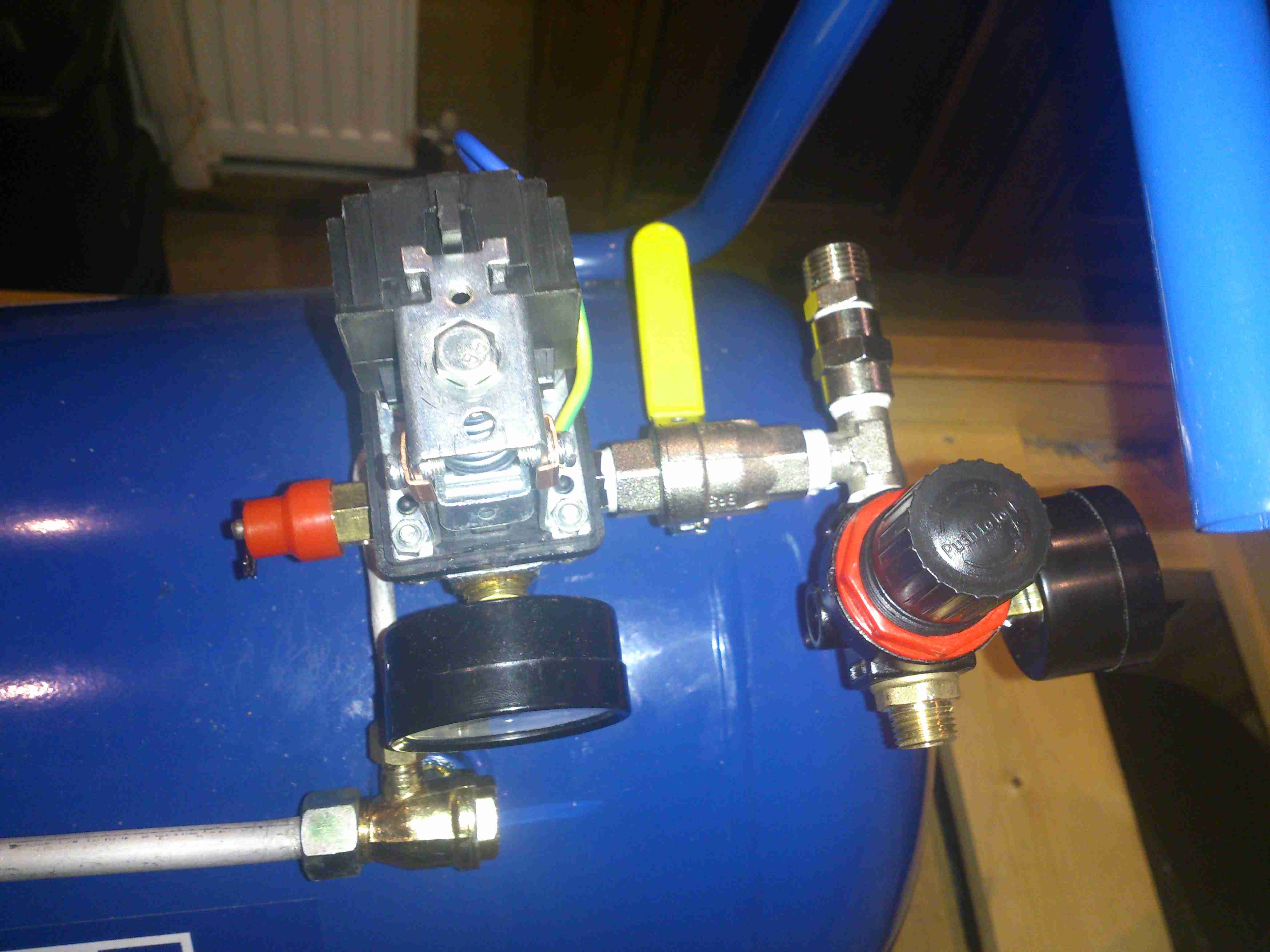
Air Fittings
Compressor control remains on top of the tank, the pressure switch & relief valve centre. After an isolation valve, the feed splits, the regulator installed will be feeding the air horn with 20PSI, replacing the existing automotive-style 12v air pump. The currently open fitting will be routed to a quick connect on the bulkhead. This will be accessible from the front deck, an air hose can be fitted to get a supply anywhere on board.
More to come when the rest of the system gets installed!
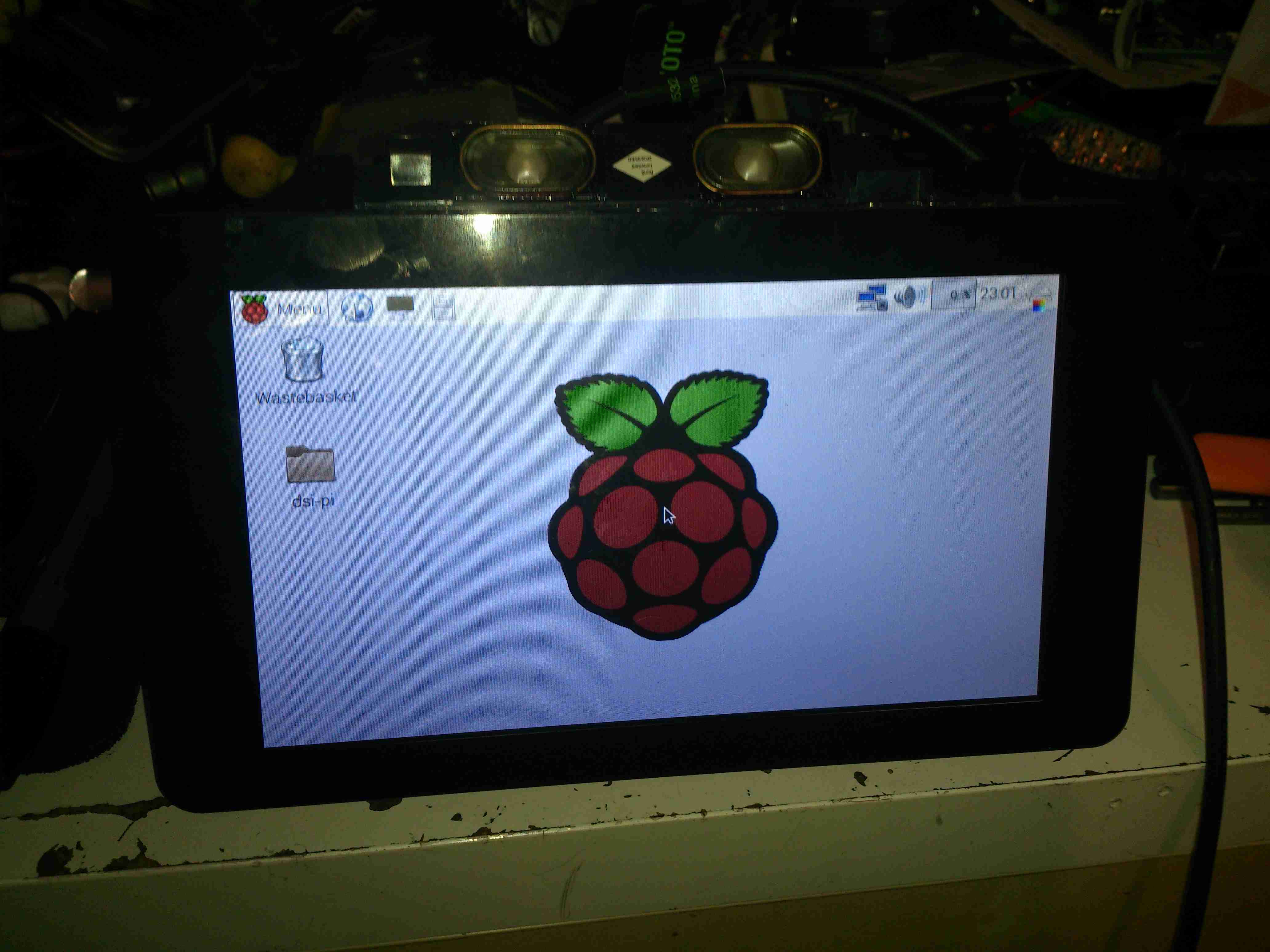
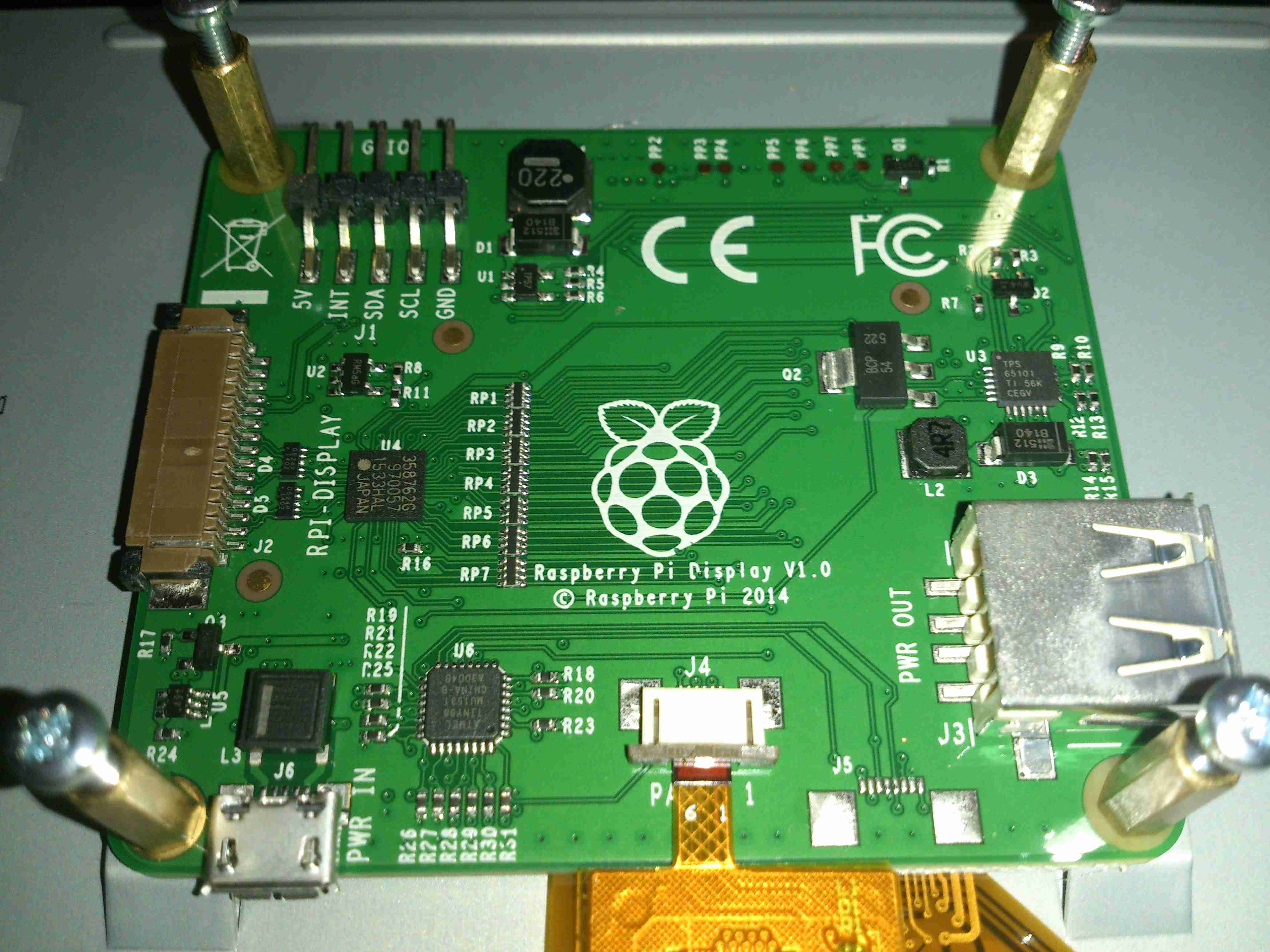
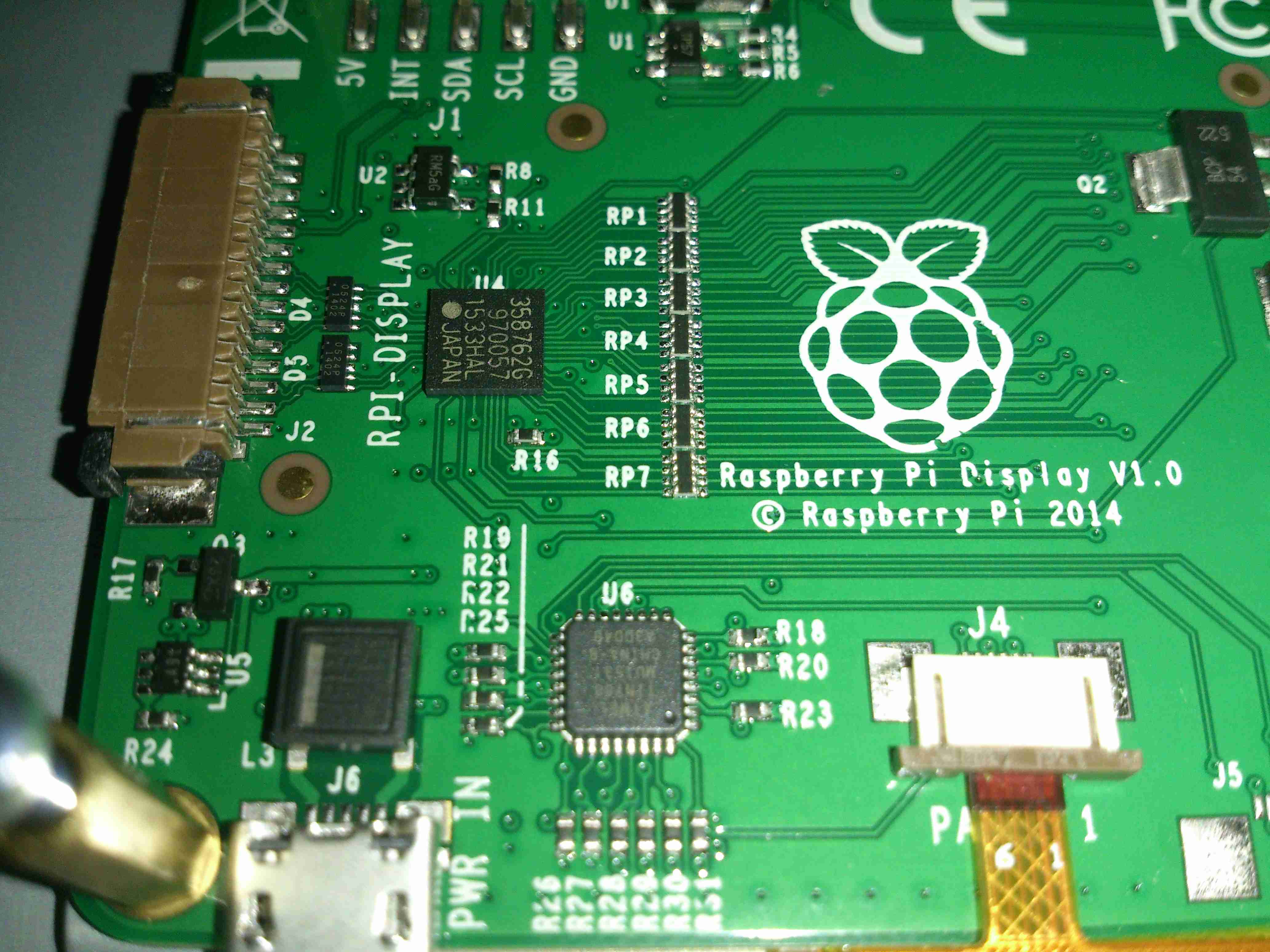
Finally the Raspberry Pi Foundation have released an official LCD for the DSI connector on the Pi. When these were announced, I placed an order straight away, but due to demand it’s taken quite a while for it to arrive in the post.
Interface PCB
The LCD itself is an RGB panel, to interface the Pi via the MIPI DSI port, some signal conversion is required. A small PCB is mounted on the back of the LCD to do this conversion. It also handles the power supply rails required by the LCD itself & interfacing the touch screen.
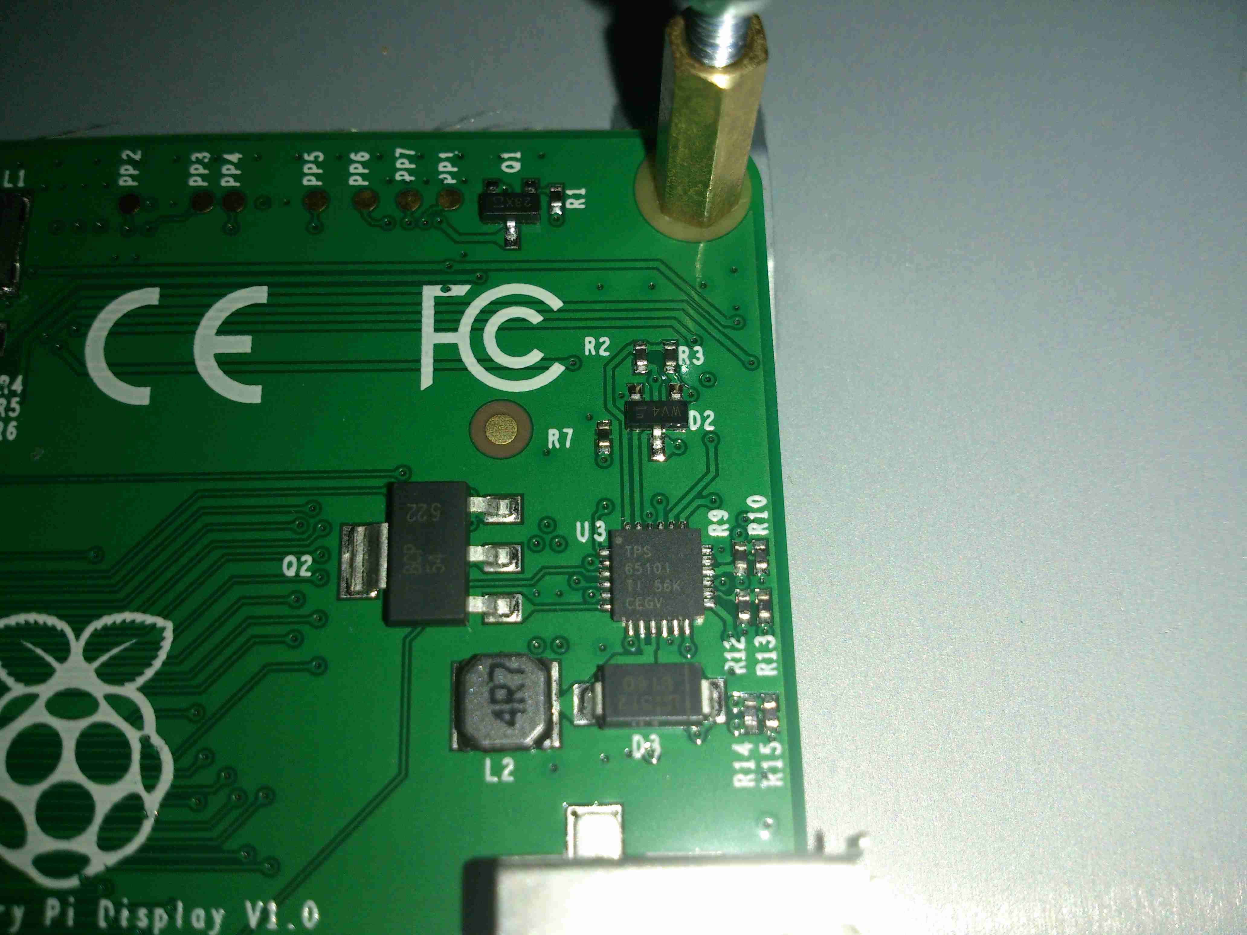
LCD Power Supply
Taking care of the power supply is a Texas Instruments TPS65101 triple output LCD power supply IC. This also has a built in linear regulator to supply 3.3v for the rest of the circuitry on board. The large transistor to the left of the IC is the pass transistor for this regulator.
Main Controller
The video signal comes in on the FFC connector on the left, into the BGA IC. I’ve not managed to identify this component, but it’s doing the conversion from serial video from the Pi to parallel RGB for the LCD.
There’s also an Atmel ATtiny88 on the board below the main video conversion IC, not sure what this is doing.
The touch controller itself is mounted on the flex of the LCD, in this case it’s a FT5406.
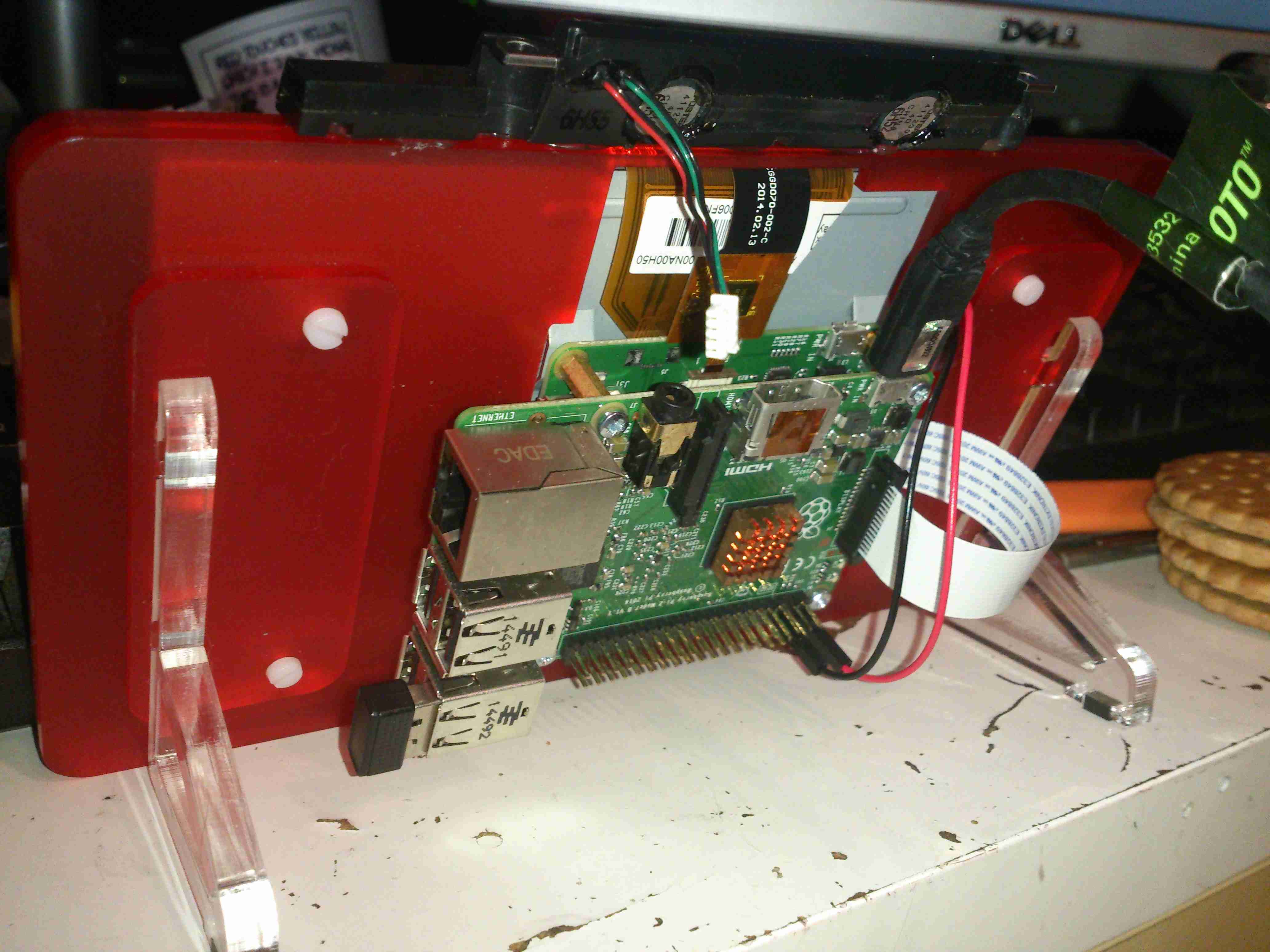
Raspberry Pi LCD
Here’s the LCD in operation. It’s not the highest resolution out there, but it leaves the GPIO & HDMI ports free for other uses.
Pi Mounted
The Pi screws to the back of the LCD & is connected with a flat flex cable & a pair of power jumpers. I’ve added a couple of small speakers to the top edge of the LCD to provide sound. (More to come on this bit).
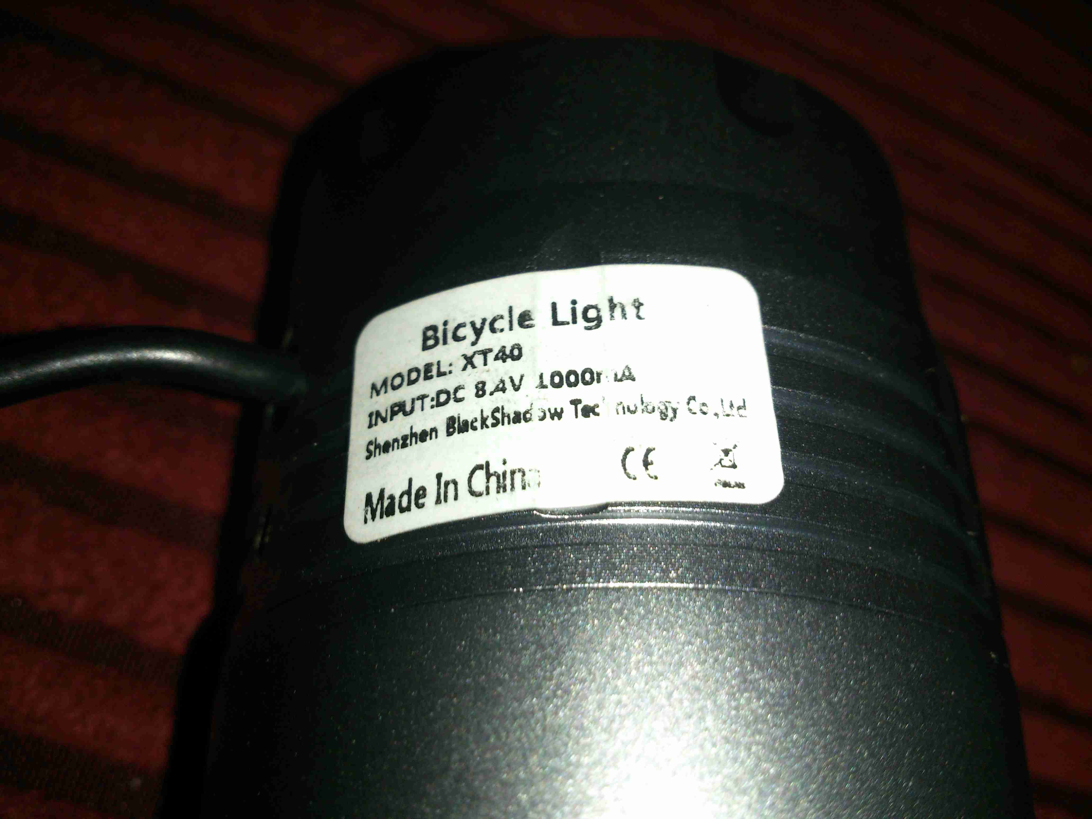
Here’s another torch from eBay, this time with 5 Cree XML-T6 LEDs.
Label
Having 5 Cree LEDs rated at up to 3A a piece, this light has the capacity to draw about 50W from it’s power supply. In this case though, current draw is about 1.5A at 12v input on the full brightness setting.
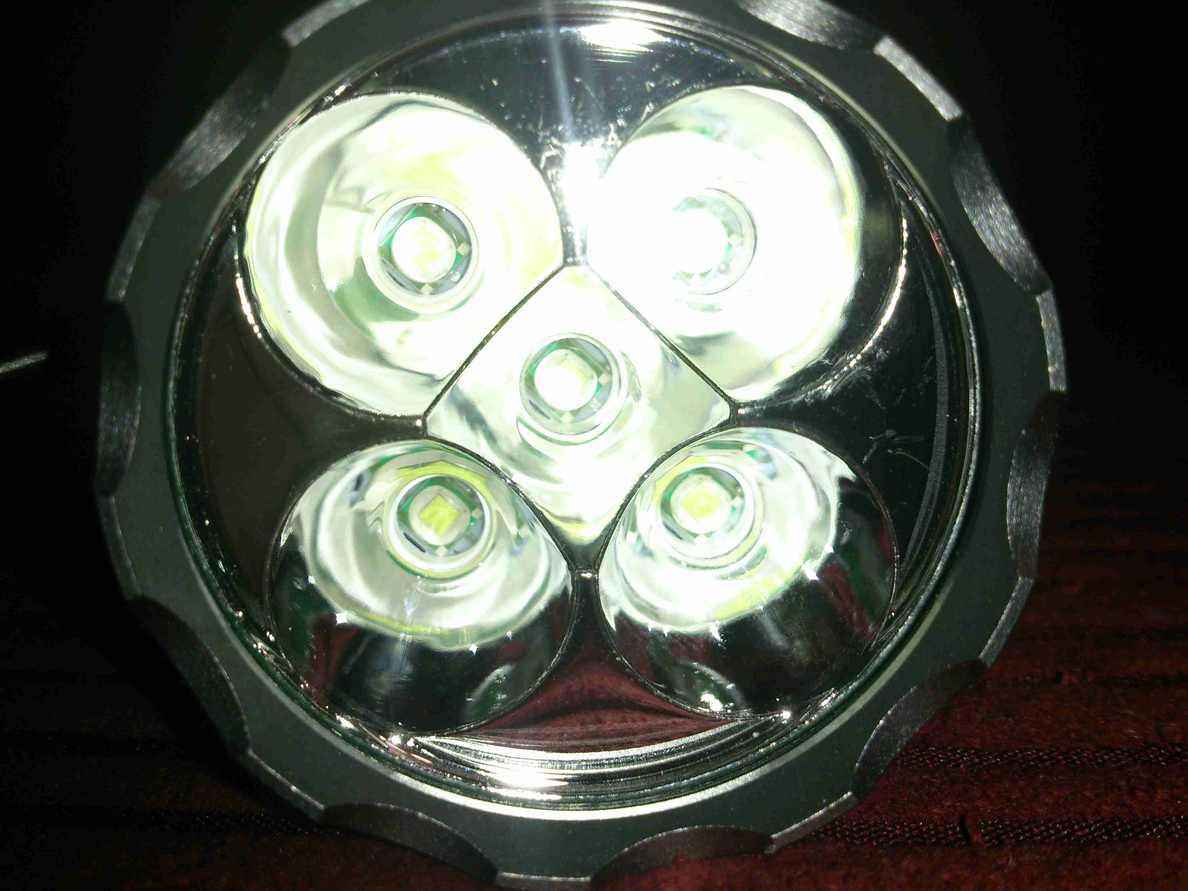
Cree LED Torch
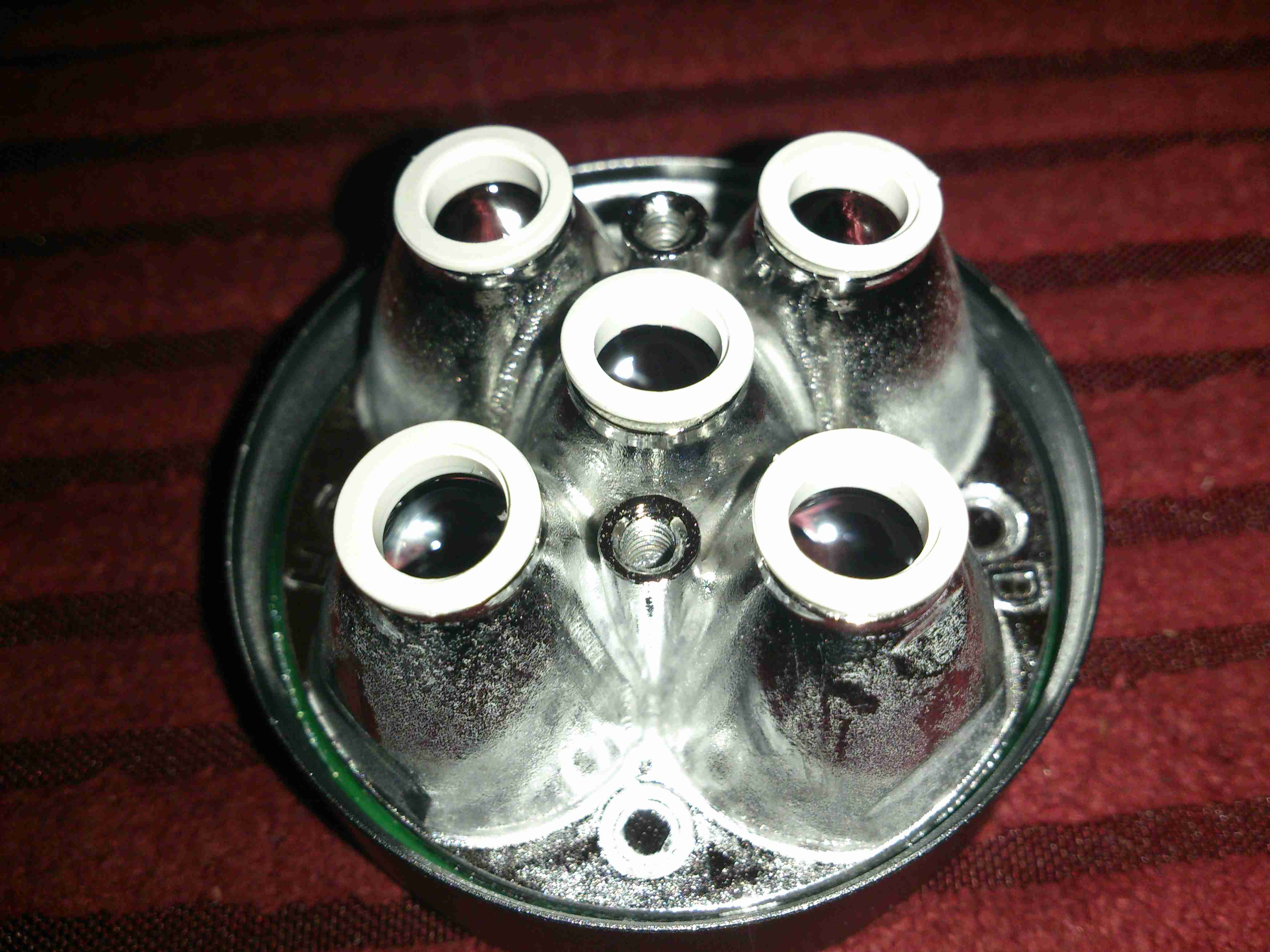
Here’s the LEDs mounted into the reflector. Fitting this many high power LEDs into a small space requires some serious heatsinking. The casing is made of machined aluminium.
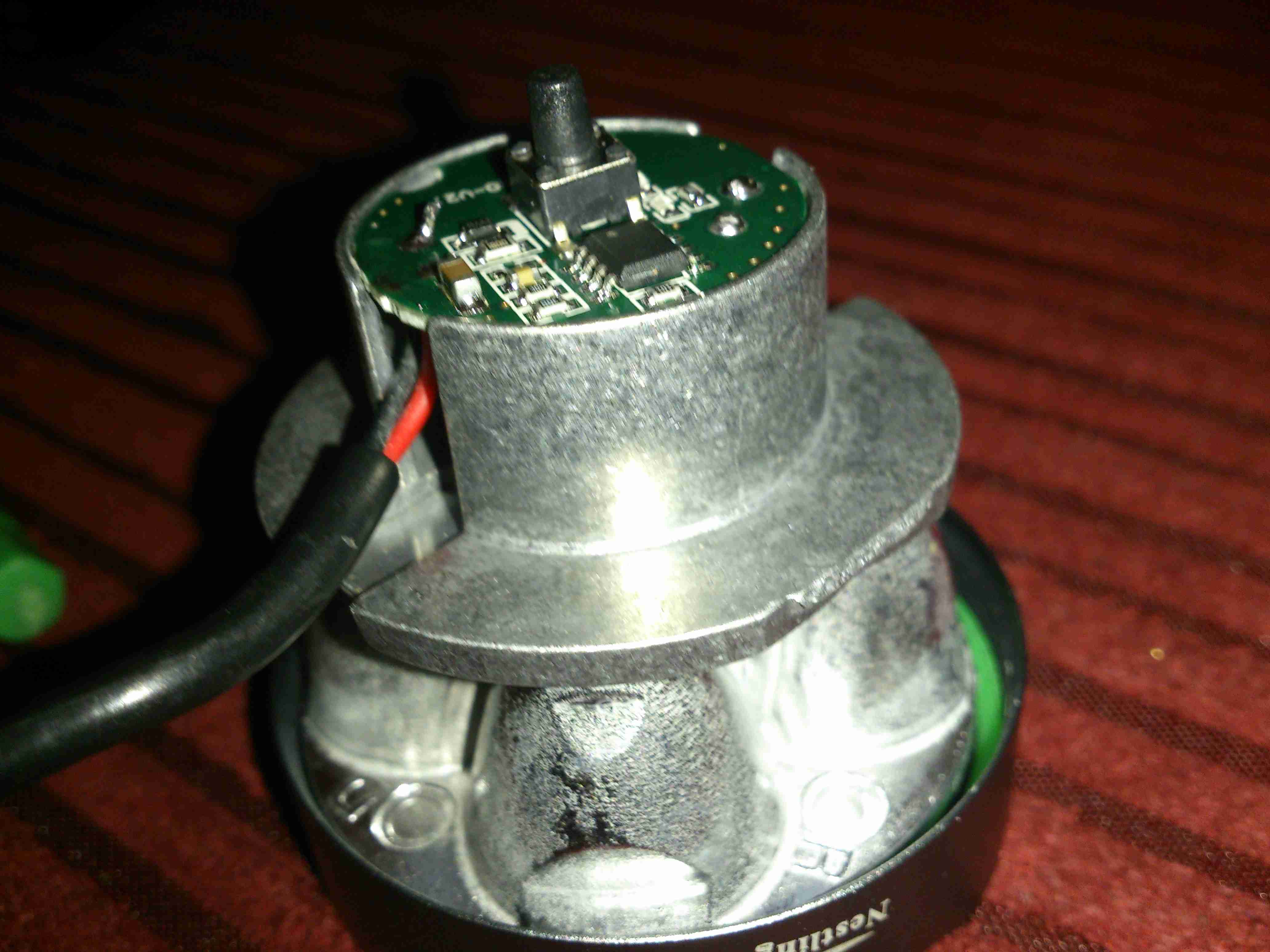
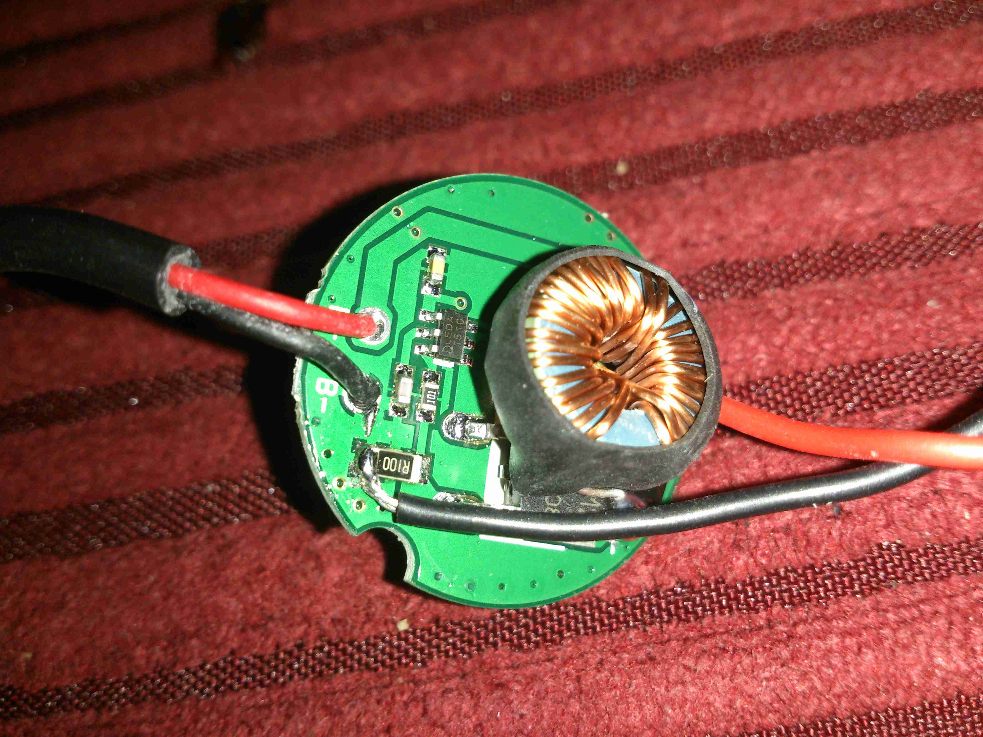
LED Module
Unscrewing the front bezel allows the internals to come out. The core frame & reflector is all cast alloy as well, for heatsinking the LEDs. The controller PCB is mounted into a recess in the back of the LED mount.
Controller
Here’s the controller itself. The usual small microcontroller is present, for the multiple modes, and handling the momentary power switch.
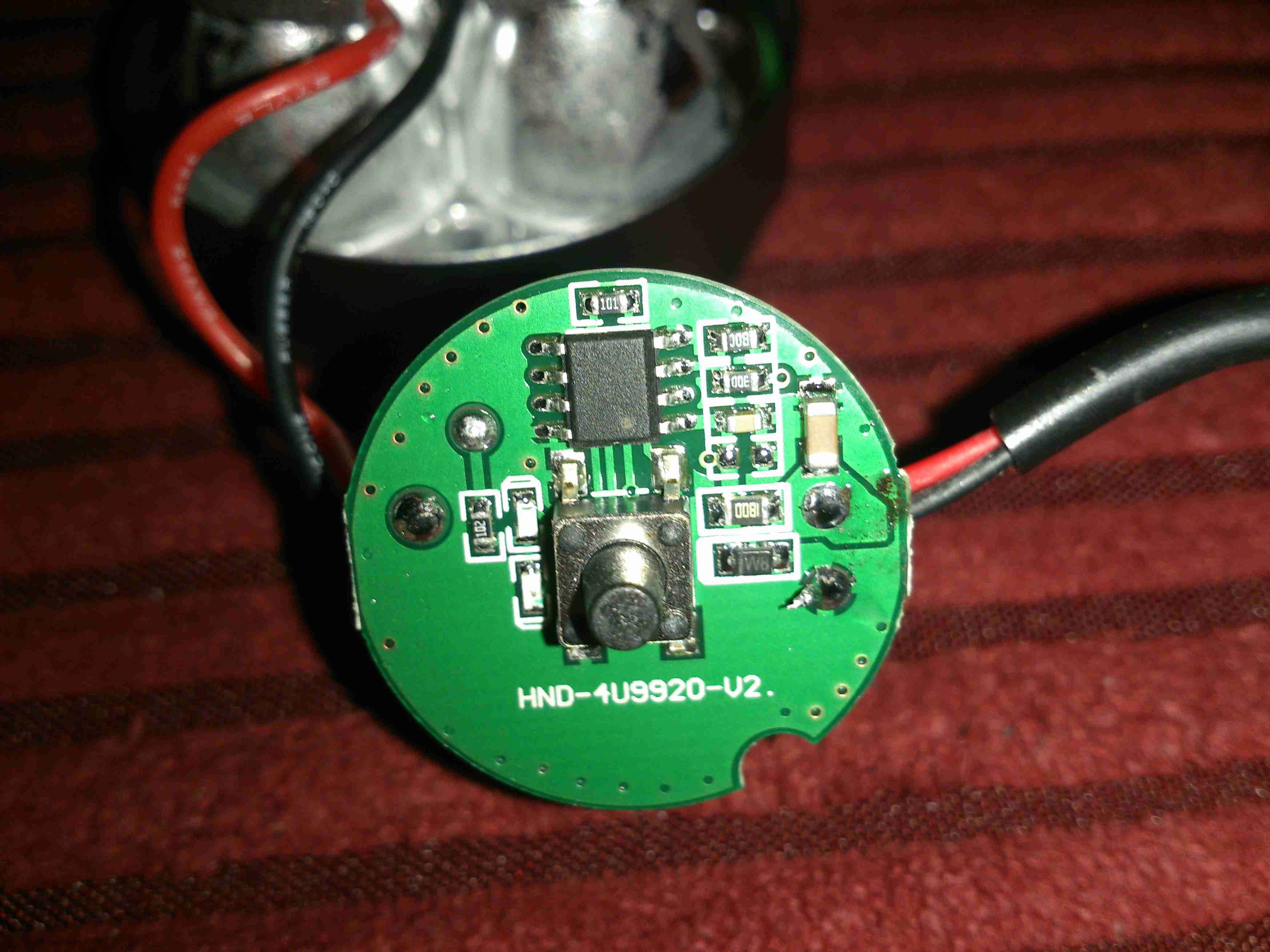
Switching Inductor
As all the LEDs on this torch are connected in series, their forward voltage is ~12-15v. The battery is an 8.4v Li-Ion pack, so some boost conversion is required. This is handled by the circuitry on the other side of the board, with this large power inductor.
Reflector
The reflector screws onto the front of the LED array, centered in place with some plastic grommets around the LEDs themselves.
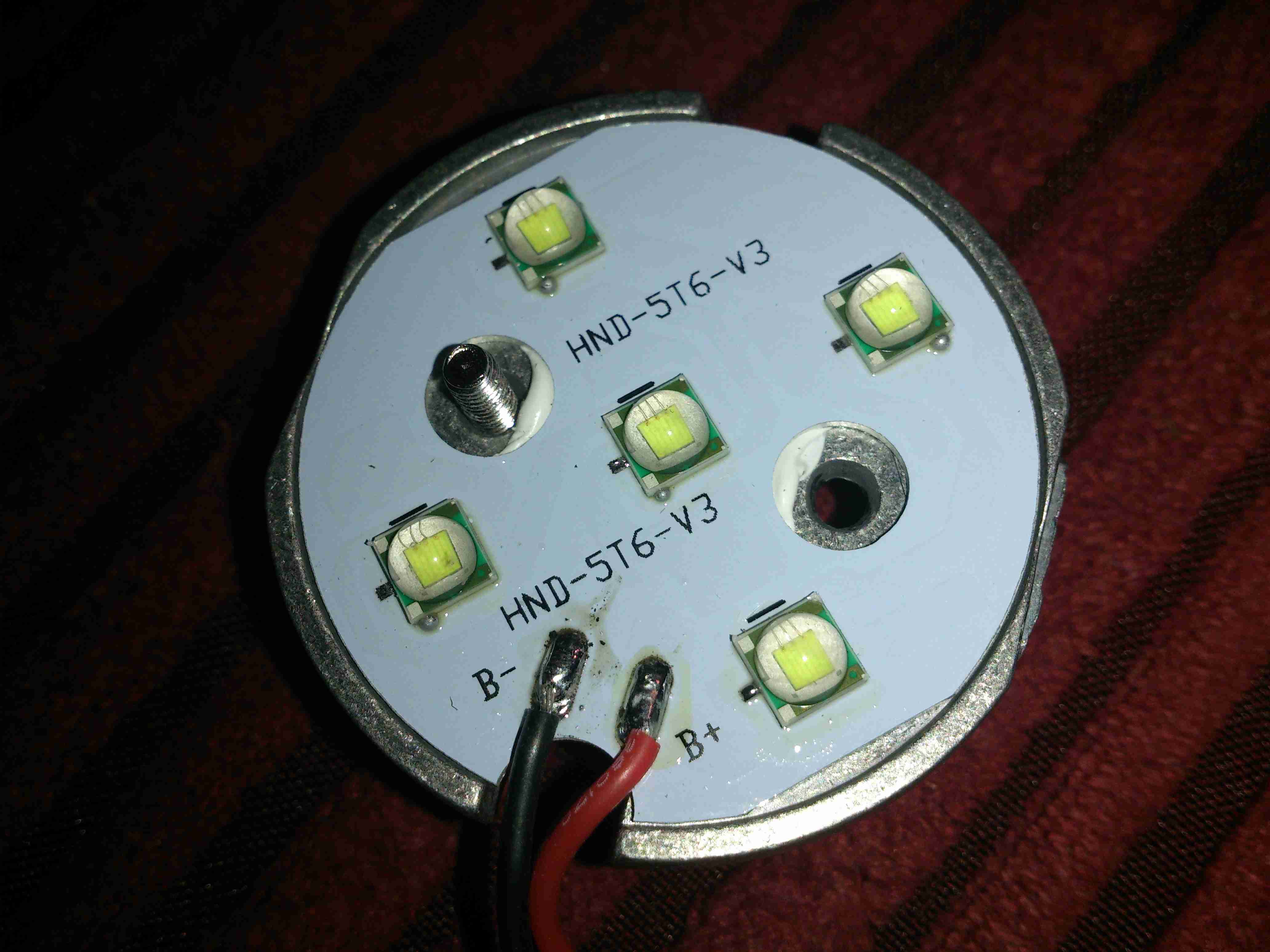
LED Array
Finally for the torch, the LED array itself. This is attached to the frame with some thermal adhesive, and the LEDs themselves are mounted on an aluminium-core PCB for better heat transfer.
This module unsurprisingly generates quite some heat, so I have improved the thermal transfer to the outer case with some thermal grease around the outer edge.
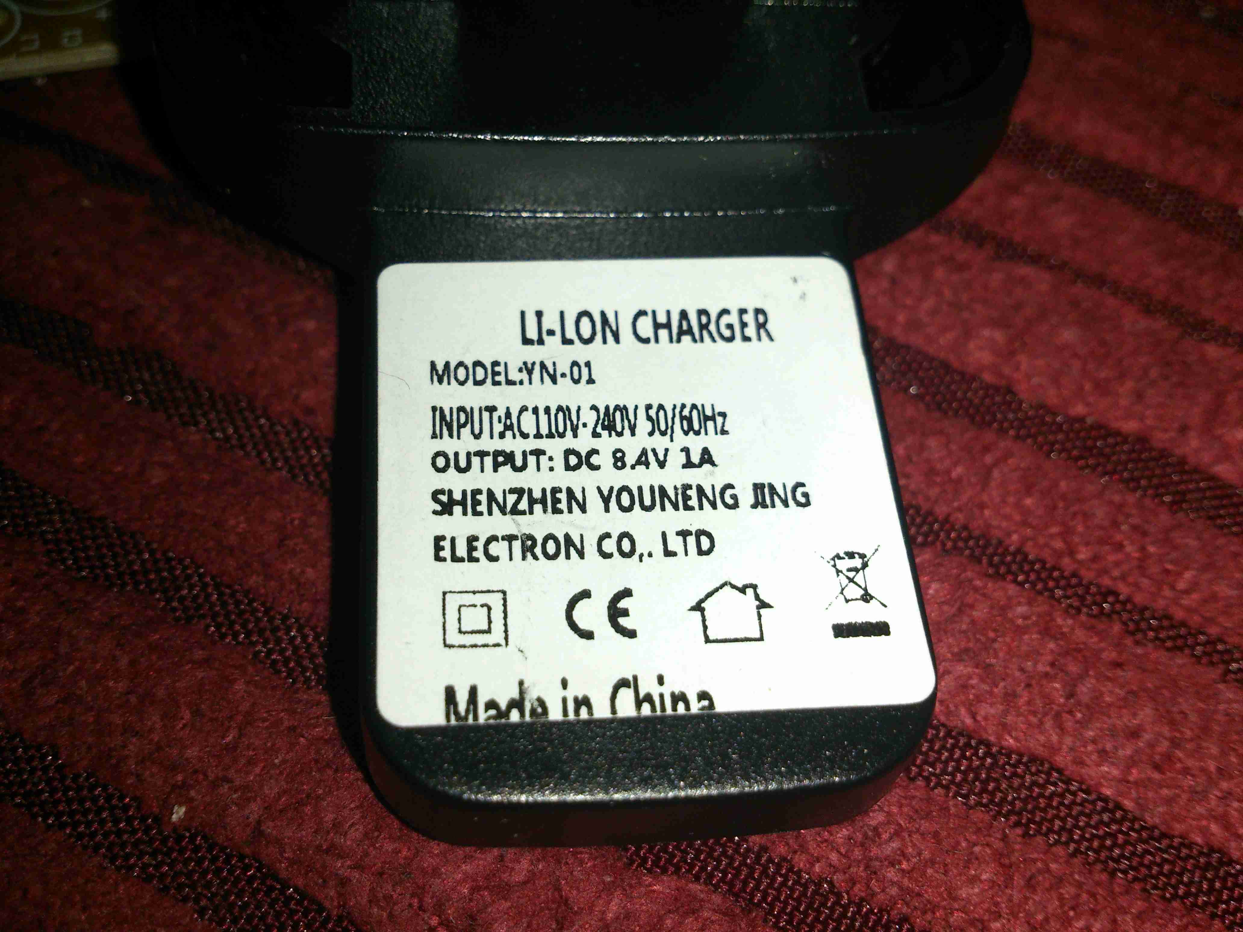
Charger
The supplied charger is the usual Chinese cheapy affair, claiming an output current of 1A at 8.4v. I never use these chargers, so they get butchered instead.
Charger PCB
Here’s the main PCB. Overall the construction isn’t that bad, the input mains is full-wave rectified, but there is little in the way of RFI filtering. The supply is fused, but with an absolutely tiny glass affair that I seriously doubt has the ability to clear a large fault current.
Like many cheap supplies, the output wiring is very thin, it’s capacity to carry 1A is questionable.
PCB Reverse
On the reverse side, there’s a nice large gap between the mains side & the low voltage output. There’s even an anti-tracking slot under the optoisolator.
During the replacement of the networking onboard nb Tanya Louise with gigabit, the main 8-port distribution switch was also changed. Here’s a quick teardown of the old one.
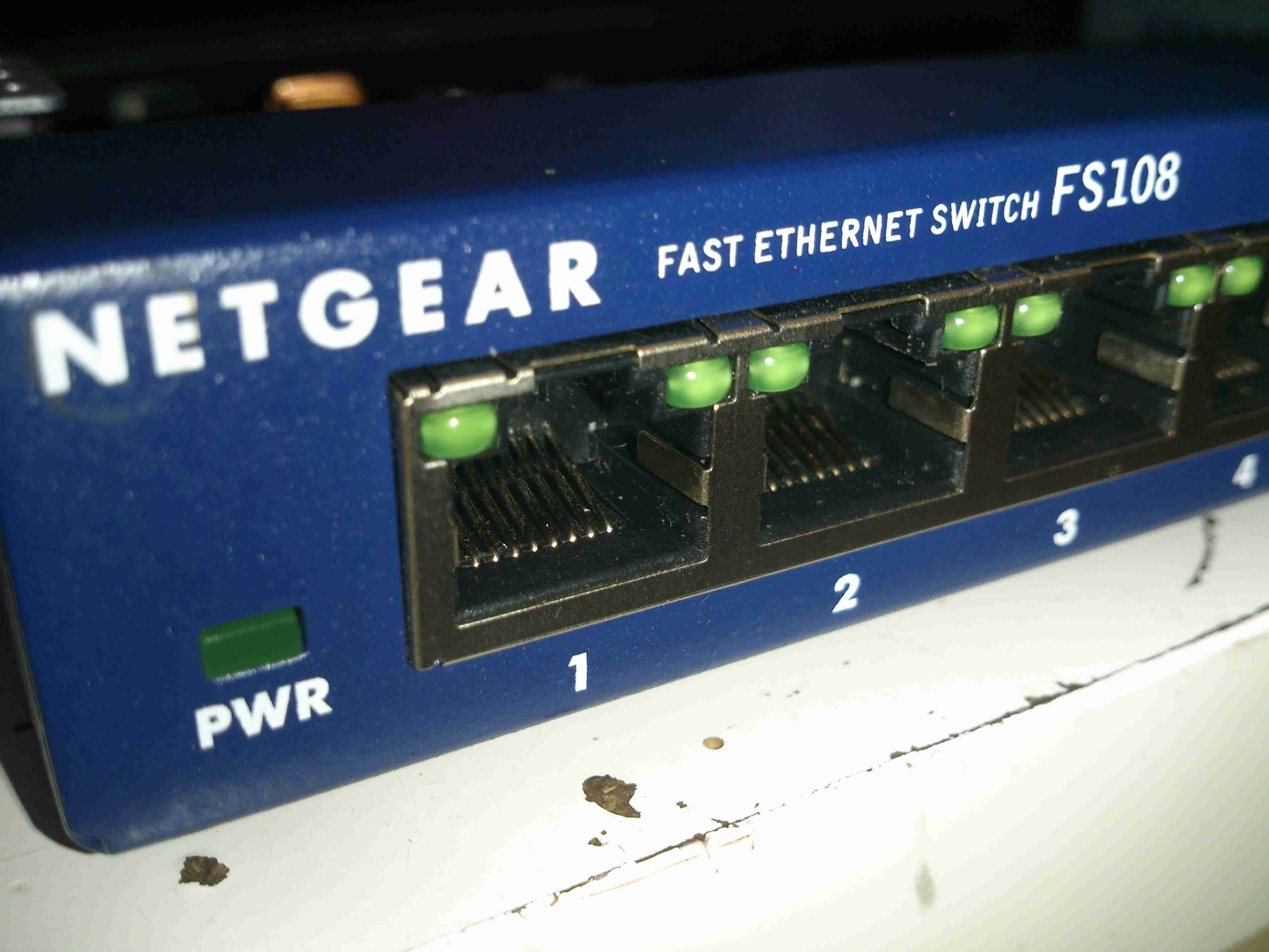
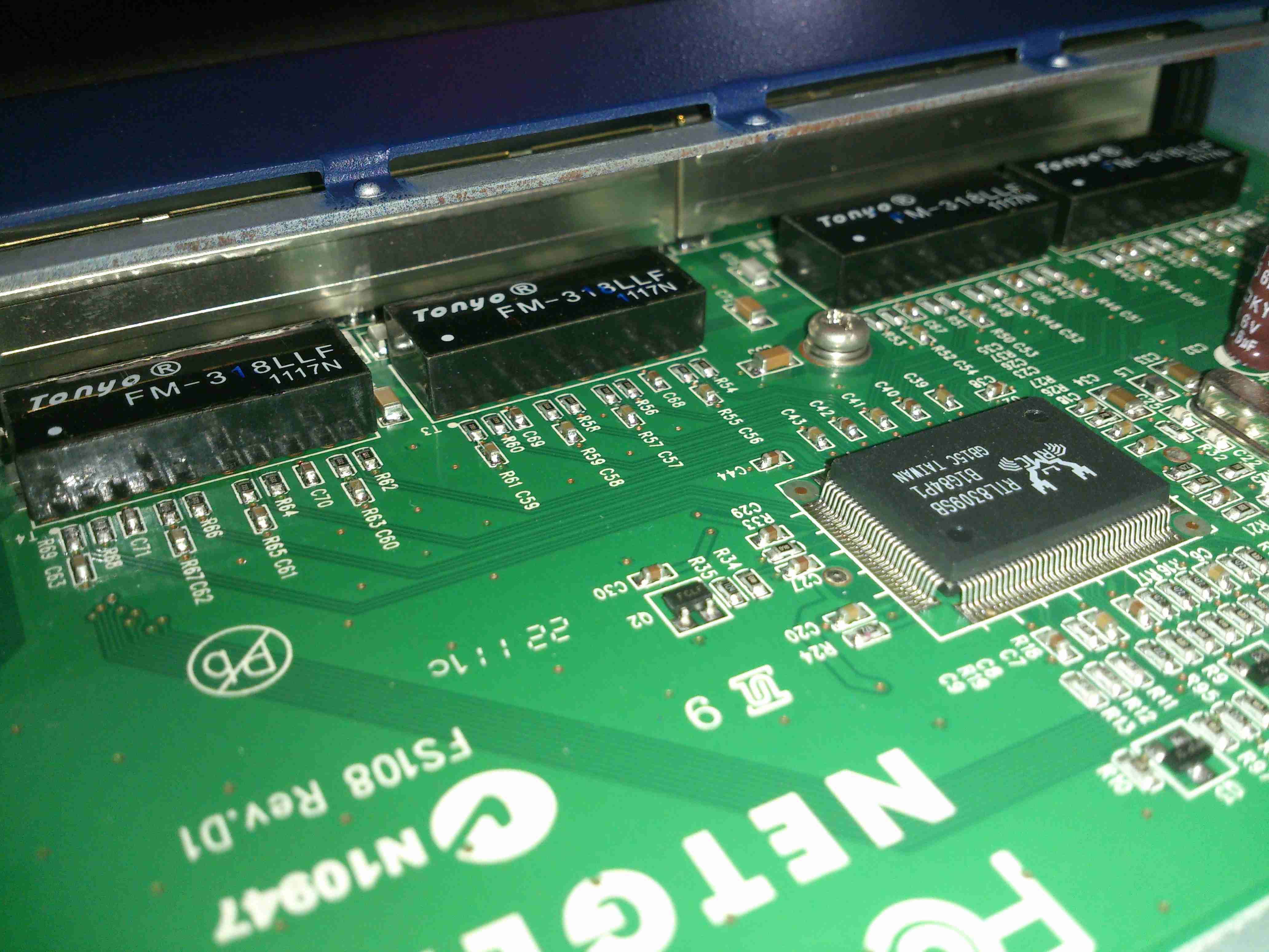
Netgear FS108
This has been quite a reliable switch for the internal networking on board, but the time has come to switch over to something a little faster. This switch will be getting repurposed for the slower devices on my network, such as the radiation monitor & the raspberry Pi systems.
Cover Removed
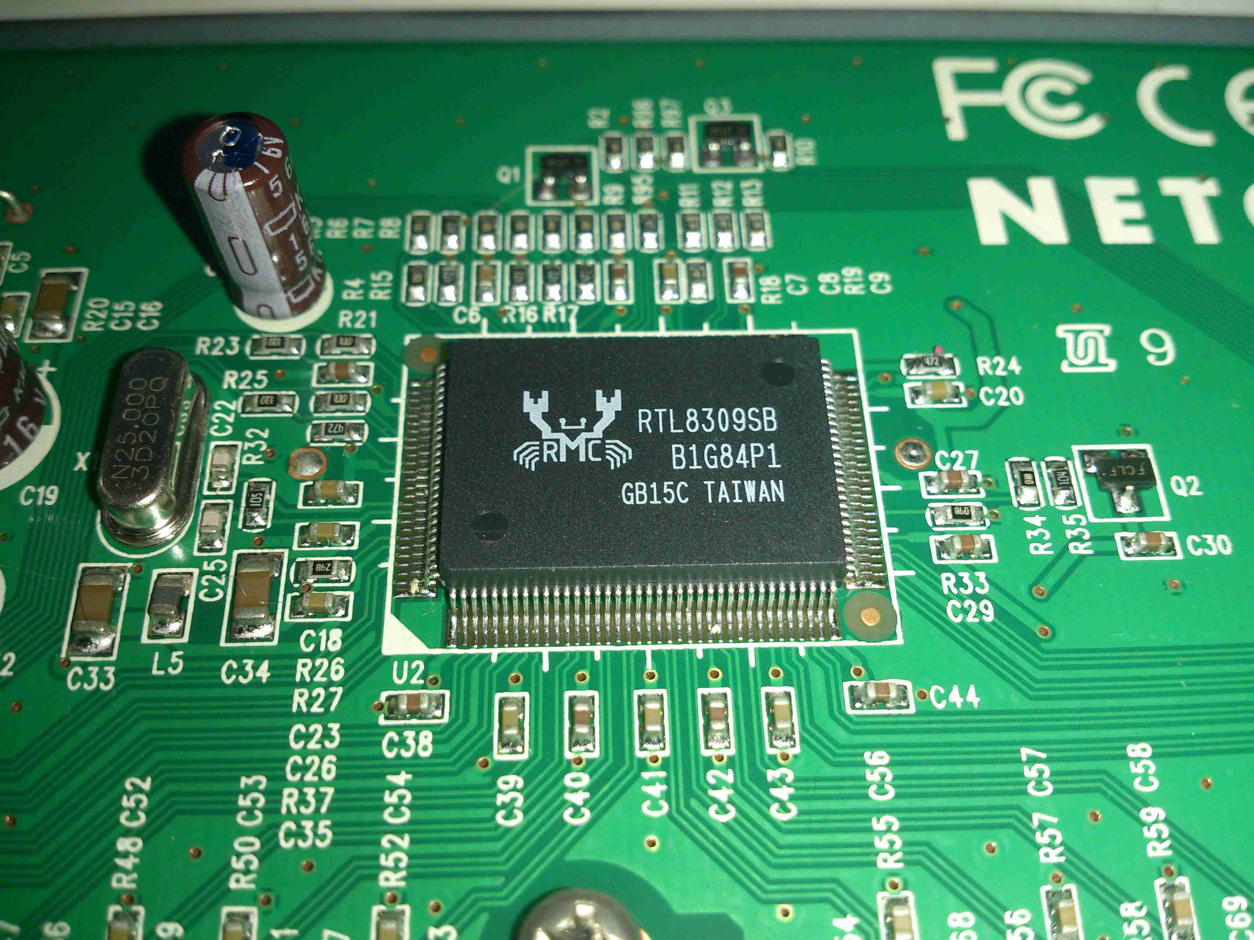
Here’s the top removed from the switch. It’s a very simple construction, with a small power supply section & the main switch IC in the centre.
Main Switch IC
All the magic happens in this main IC, a Realtek RTL8309SB Fast Ethernet switch. This is a feature-packed IC, with support for VLAN tagging, but being in a small unmanaged switch the extra features aren’t used.
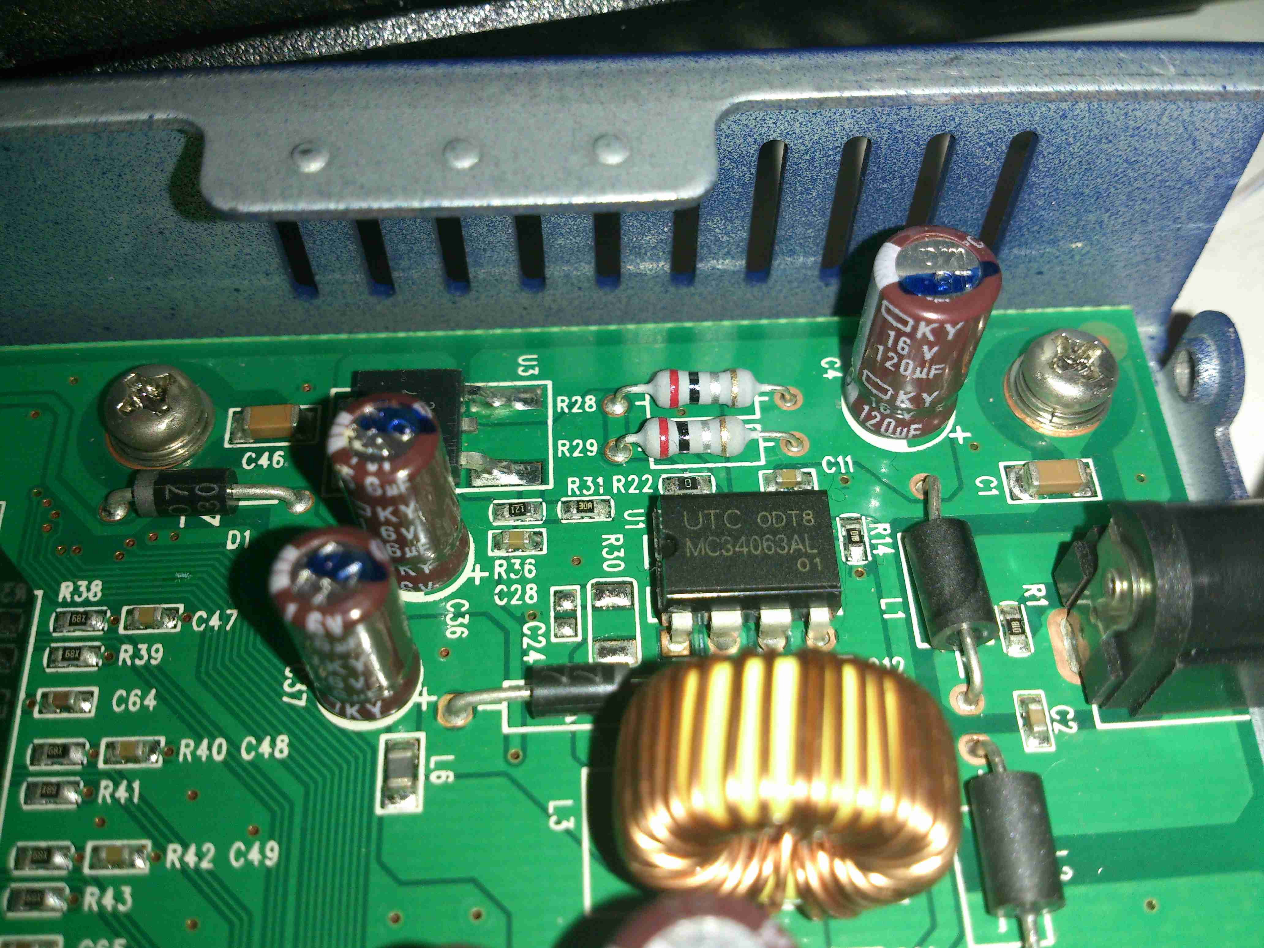
Power Supply
Main power supply is provided by a jelly bean MC34063 DC-DC converter, and an adjustable LM1117 linear regulator. Nothing much special here.
Ethernet Magnetics
The only other parts are the magnetics for the ethernet interfaces, behind the ports themselves.
Since the boat was still running it’s internal network on 10/100M speeds, an upgrade was decided on, the internal WiFi signal strength was also pretty poor further than a few feet from the NOC.
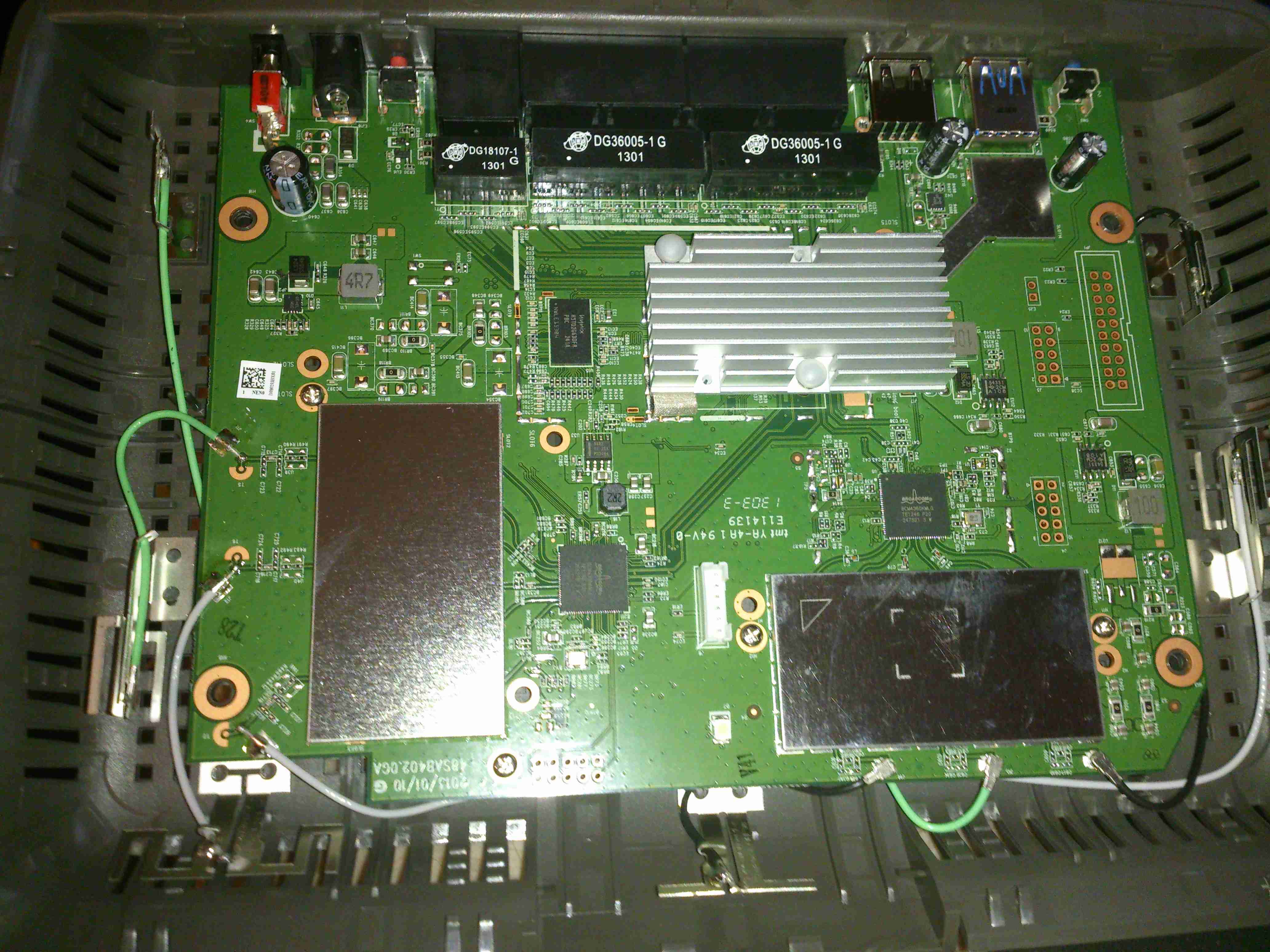
The new router is a Cisco/Linksys AC1750 model, with gigabit networking, and full 802.11ac 2.4/5GHz Wireless. This router also has a built in media server, print server, USB3 & USB2.
PCB Overview
Teardown time! Here’s the router with the cover removed. Most of the fun stuff is hidden under the shields, but these aren’t fully soldered down & the covers are removable. The 6 antennas can be seen spaced around the edge of the housing, the main CPU is under the large heatsink upper centre. The radio power amplifier stages are underneath the shields, while the main RF transceivers are just outside the shields.
2.4GHz Transceiver
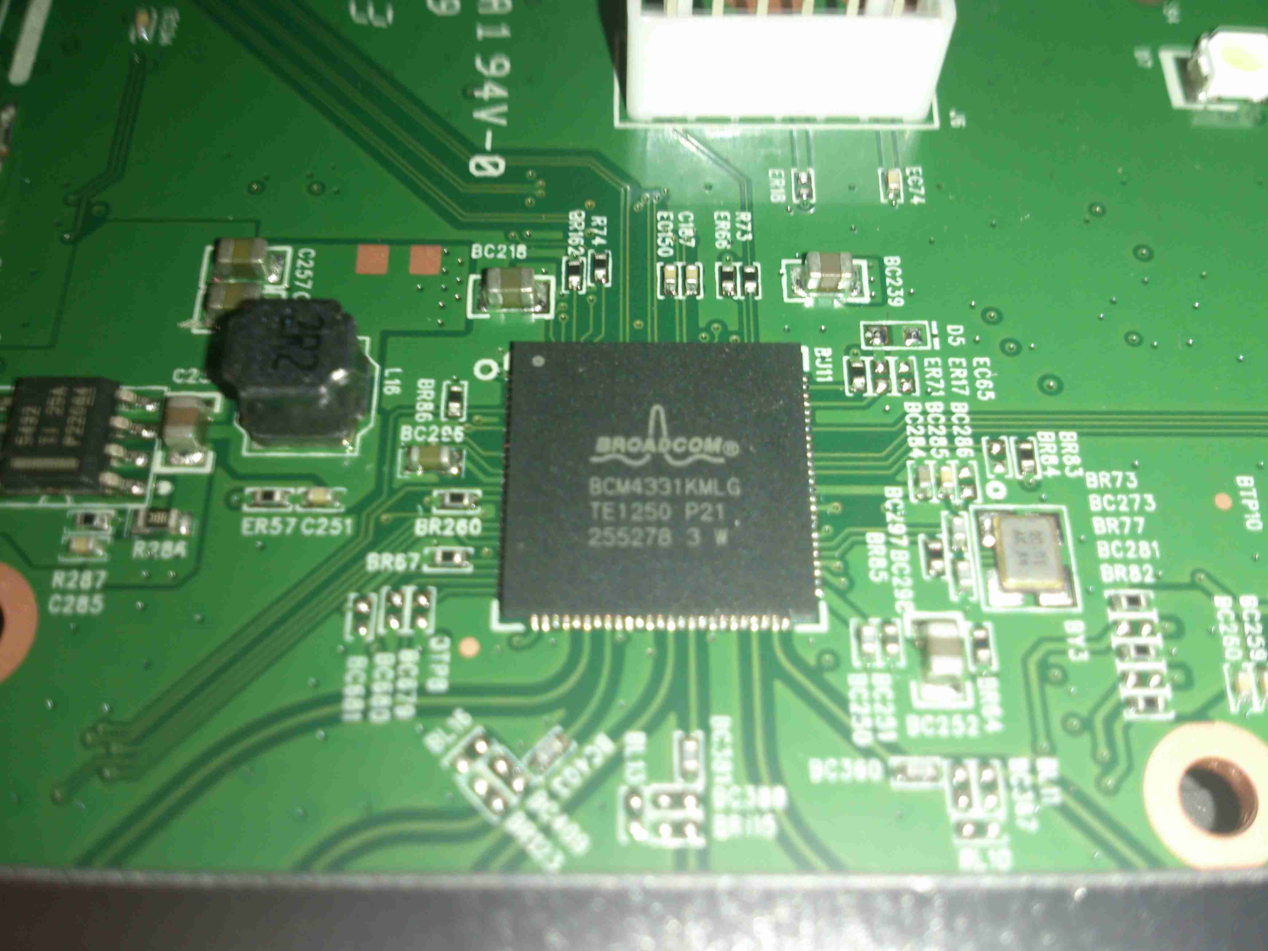
Wireless N is provided by a Broadcom BCM4331, this provides full dual-band 3×3 802.11n support. Being 3×3 it is actually 3 separate transceivers in a single package, to get much higher throughput rates of 600Mbit/s.
5GHz Transceiver
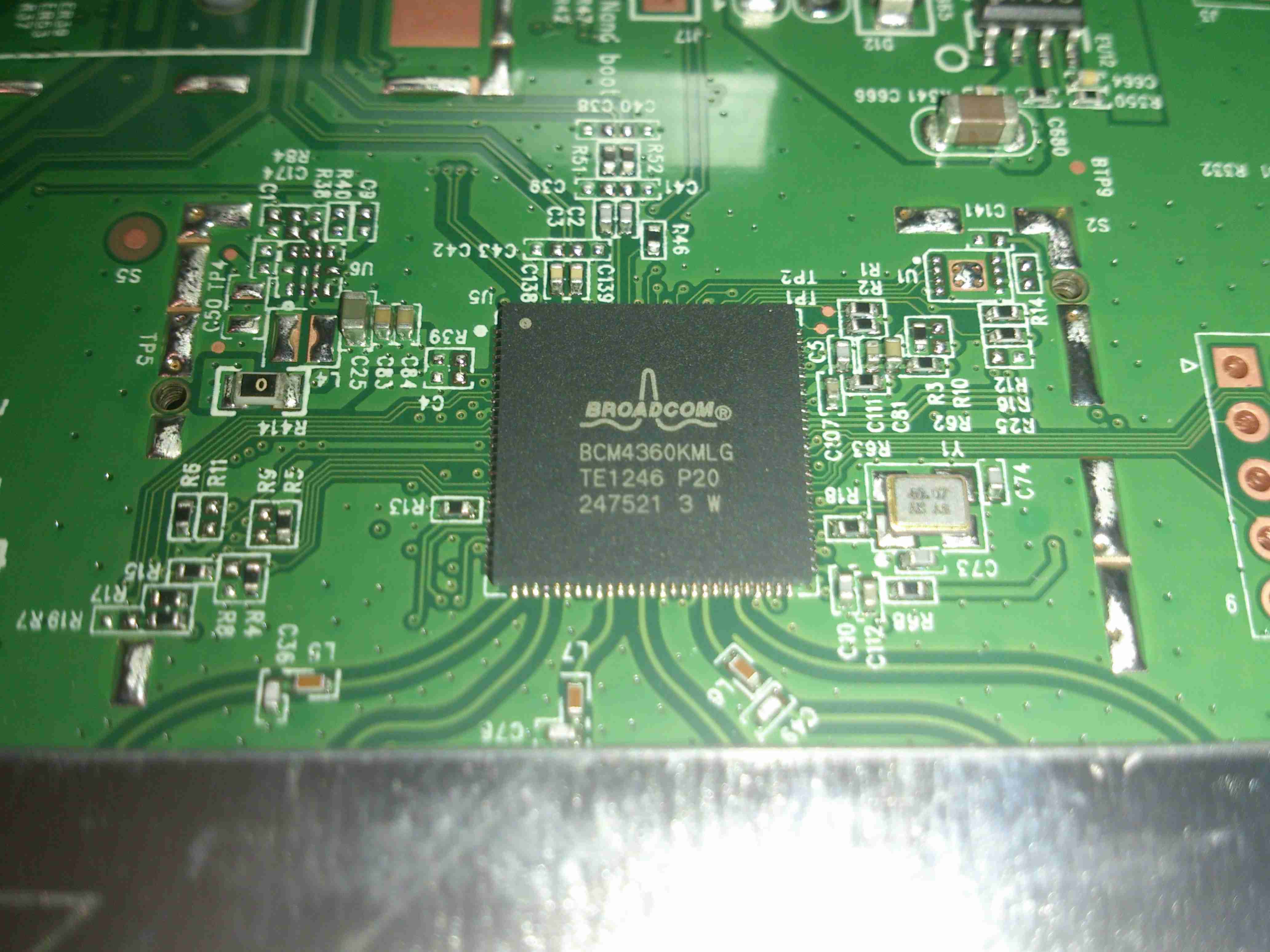
Wireless AC is provided by it’s sister IC, the BCM4360, with throughput speeds of 1.3Gbit/s. Both of these transceiver ICs connect back to the main CPU via PCI Express.
5GHz Power Amplifiers
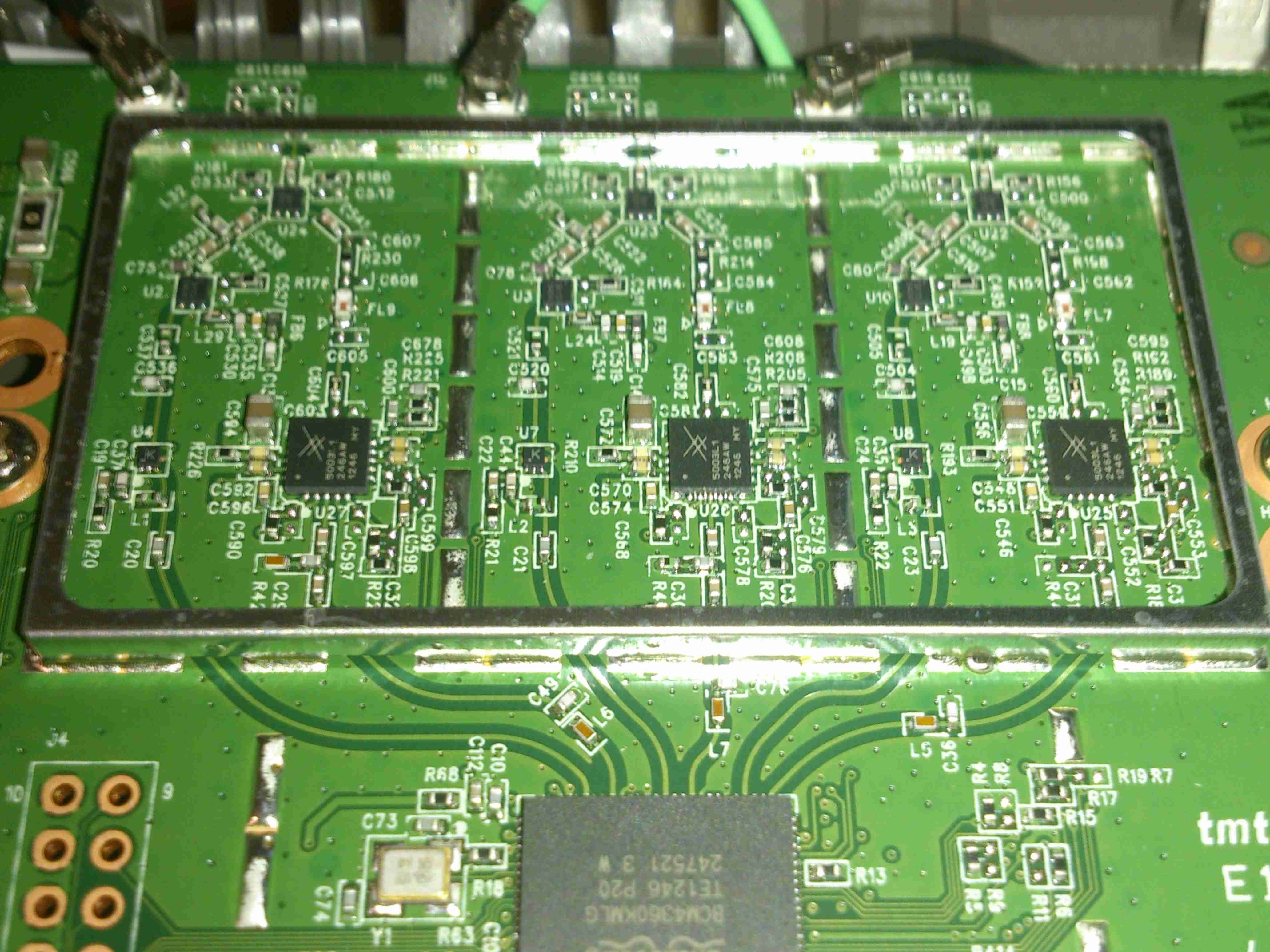
To get increased range, there are a trio of Skyworks SE5003L +23dBm 5GHz power amplifier ICs under the shield, along with the TX/RX switching & antenna matching networks. Heatsinking for these is provided by a sink screwed to the bottom side of the PCB. The outputs to the antennas can be seen at the top of the image.
2.4GHz Power Amplifiers
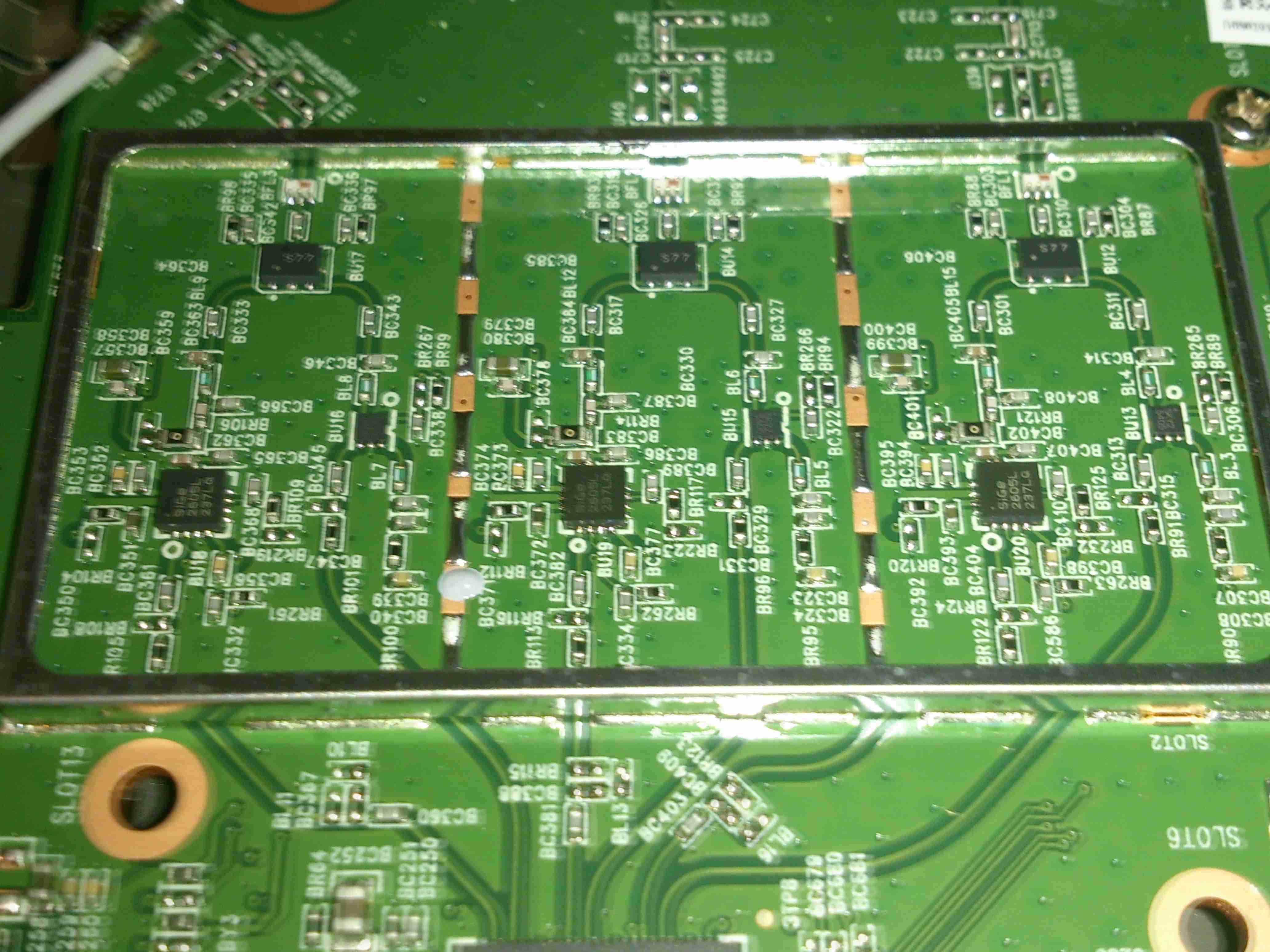
The 2.4GHz section is fitted with a trio of Skyworks SE2605L +23dBm 2.4GHz power amplifiers, with a similar heatsink arrangement under the board. Unlike the 5GHz section, the 2.4GHz antenna feeds are soldered to the PCB here instead of using connectors.
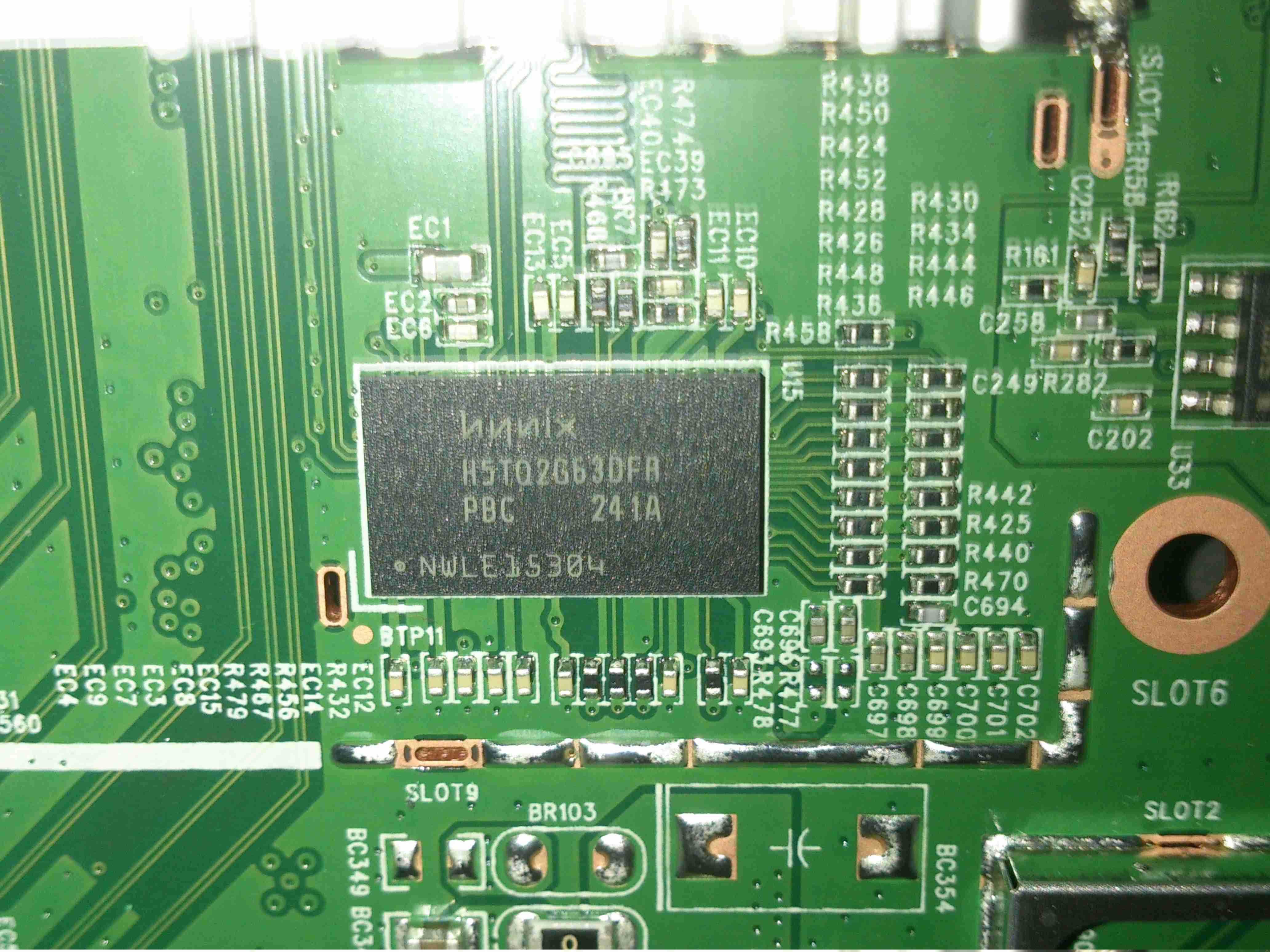
Main CPU
The main CPU is a BCM4708 Communications Processor from Broadcom, as for the other Broadcom chips in this router, very little information is available unless under NDA, but I do know it’s a dual core ARM Cortex A9 running at 1GHz, with built in 5-port gigabit ethernet switch.
CPU RAM
Working RAM for the processor is a Hynix H5TQ2G63DFA 256MB part.
More to come on the installation of the new networking, with it’s associated 4G mobile gateway connection system.
The multimode dimming/flashing modes on Chinese torches have irritated me for a while. If I buy a torch, it’s to illuminate something I’m doing, not to test if people around me have photosensitive epilepsy.
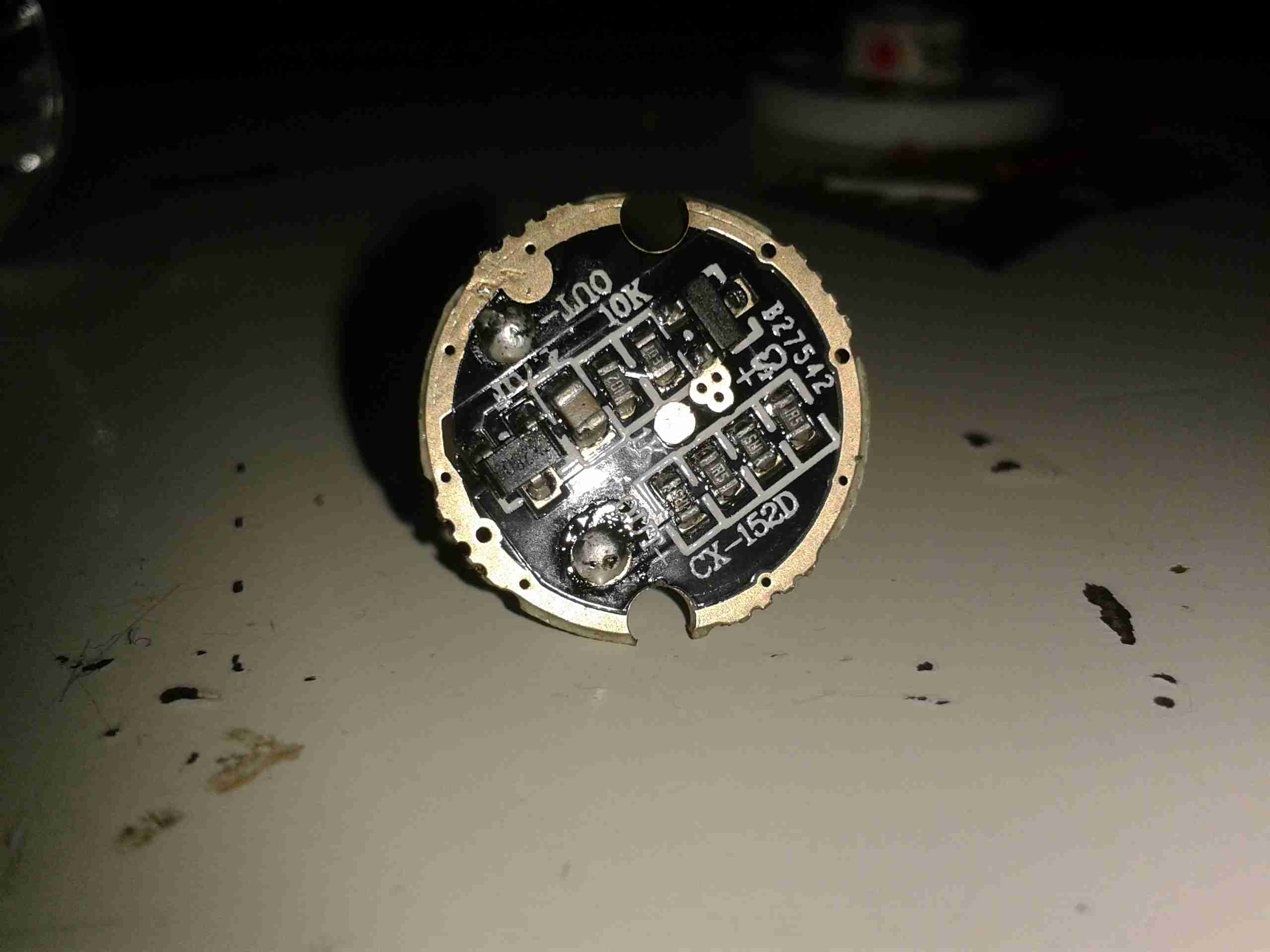
Looking at the PCB in the LED module of the torch, a couple of components are evident:
LED Driver PCB
There’s not much to this driver, it’s simply resistive for LED protection (the 4 resistors in a row at the bottom of the board).
The components at the top are the multimode circuitry. The SOT-23 IC on the left is a CX2809 LED Driver, with several modes. The SOT-23 on the right is a MOSFET, for switching the actual LED itself. I couldn’t find a datasheet for the IC itself, but I did find a schematic that seems to match up with what’s on the board.
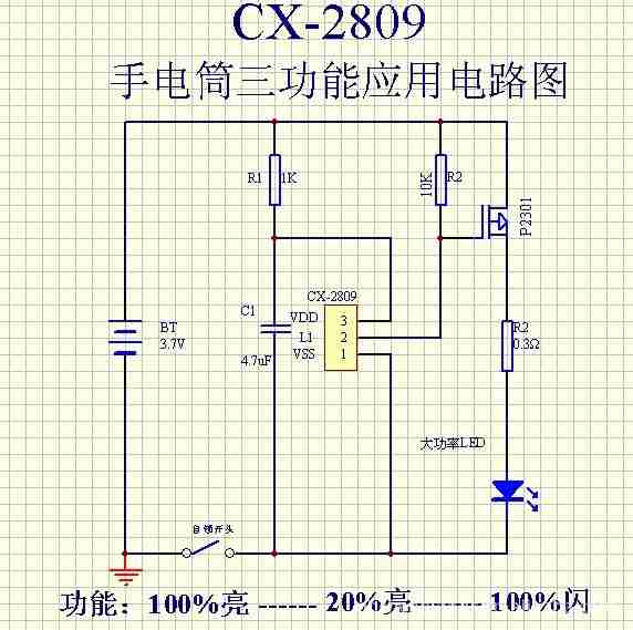
Schematic
Here’s that schematic, the only thing that needs to be done to convert the torch to single mode ON/OFF at full brightness, is to bridge out that FET.
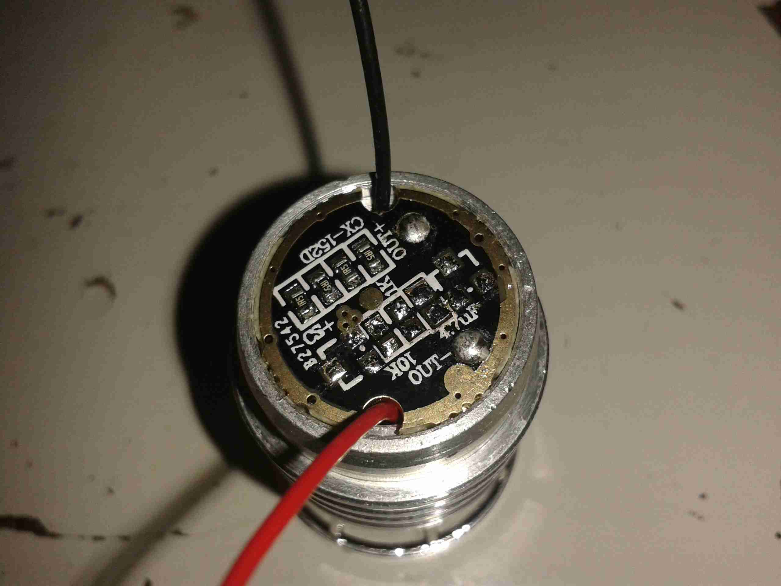
Components Desoldered
To help save the extra few mA the IC & associated circuitry will draw from the battery, I have removed all of the components involved in the multimode control. This leaves just the current limiting resistors for the LED itself.
Jumper Link
The final part above, is to install a small link across the Drain & Source pads of the FET. Now the switch controls the LED directly with no silly electronics in between. A proper torch at last.
Now the controllers have arrived, I can rejig the supplies to have proper thermal control on their cooling.
Changes Overview
Here’s the top off the PSU. The board has been added to the back panel, getting it’s 12v supply from the cable that originally fed the fan directly. Luckily there was just enough length on the temperature probe to fit it to the output rectifier heatsink without modification.
To connect to the standard 4-pin headers on the controller, I’ve spliced on a PC fan extension cable, as these fans spent their previous lives in servers, with odd custom connectors.
Fan Controller
Here’s the controller itself, the temperature probe is inserted between the main transformer & the rectifier heatsink.
I’ve set the controller to start accelerating the fan at 50°C, with full speed at 70°C.
Full Load Test
Under a full load test for 1 hour, the fan didn’t even speed up past about 40% of full power. The very high airflow from these fans is doing an excellent job of keeping the supply cool. Previously the entire case was very hot to the touch, now everything is cool & just a hint of warm air exits the vents. As the fan never runs at full speed, the noise isn’t too deafening, and immediately spools back down to minimum power when the load is removed.
In my previous post, I mentioned I’d be replacing the factory supplied charging gear with something that actually charges lithium chemistry cells correctly.
Charging Base
Here’s the base as supplied, with an indicator LED on the right hand side. This LED indicates nothing other than power being applied to the charging base. It’s just connected across the power input with a resistor. This also means that any battery left in the charger while it’s unplugged will discharge itself through this LED over time. Great design there China!
PCB Removed
Here I’ve removed the PCB – there’s no need for it to be taking up any space, as it’s just a complete waste of copper clad board in the first place. The battery tabs have been desoldered & hot snot used to secure them into the plastic casing.
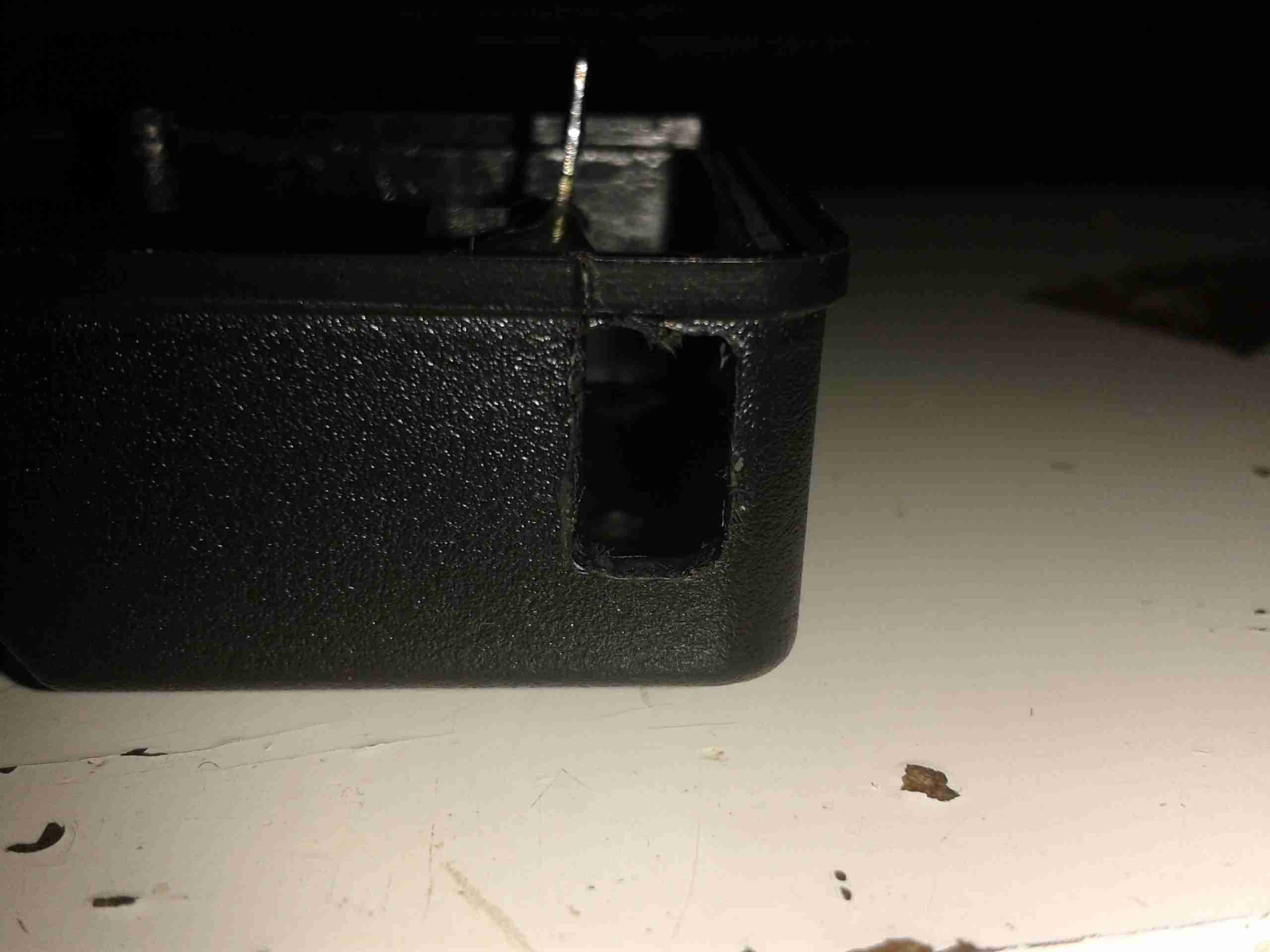
USB Hole
The charger modules I use are USB powered, so a small hole has been routed out in the casing to allow access to the port.
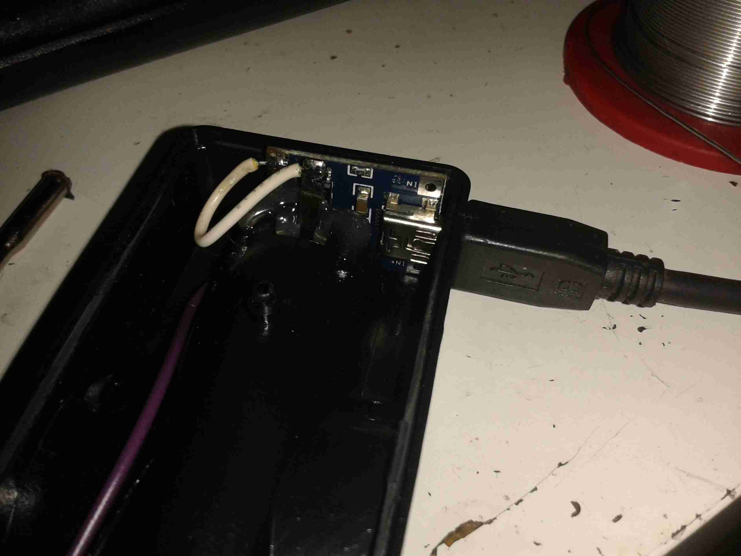
Charging Module
Here the charging module has been installed & wired to the battery tabs. Output is now a nice 4.18v, and will automatically stop charging when the cell is full.
Safety has been restored!
73s for now folks!
Tip Jar
If you’ve found my content useful, please consider leaving a donation by clicking the Tip Jar below!
All collected funds go towards new content & the costs of keeping the server online.