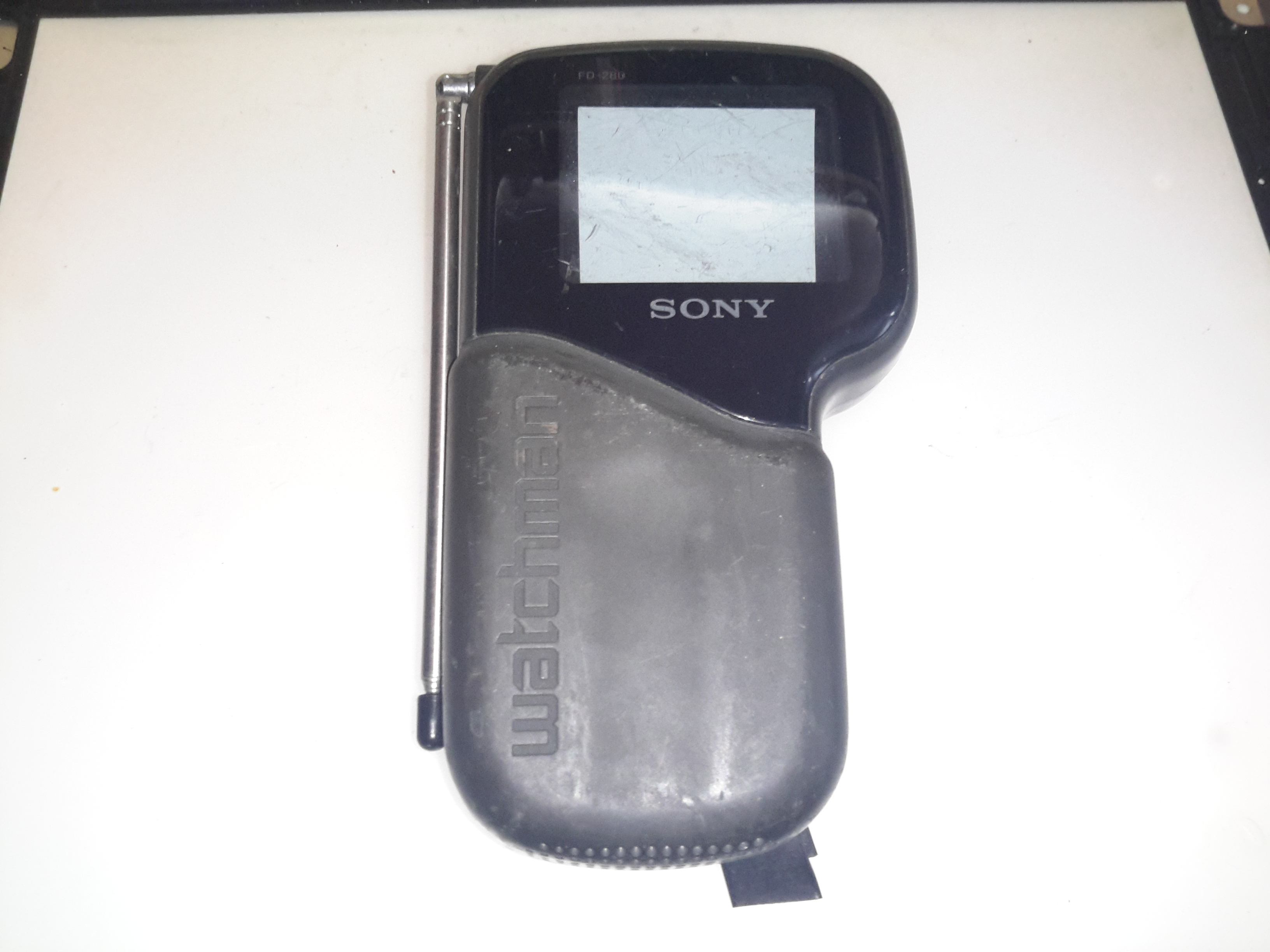
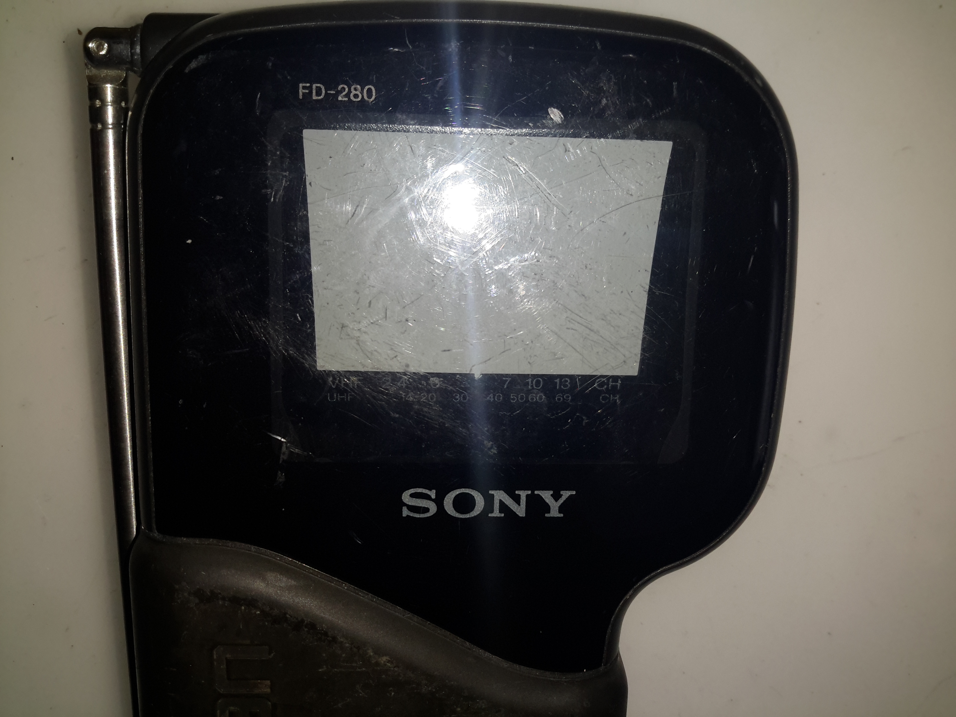
Here’s another Sony Flat CRT TV, the FD0280. This one was apparently the last to use CRT technology, later devices were LCD based. This one certainly doesn’t feel as well made as the last one, with no metal parts at all in the frame, just moulded plastic.
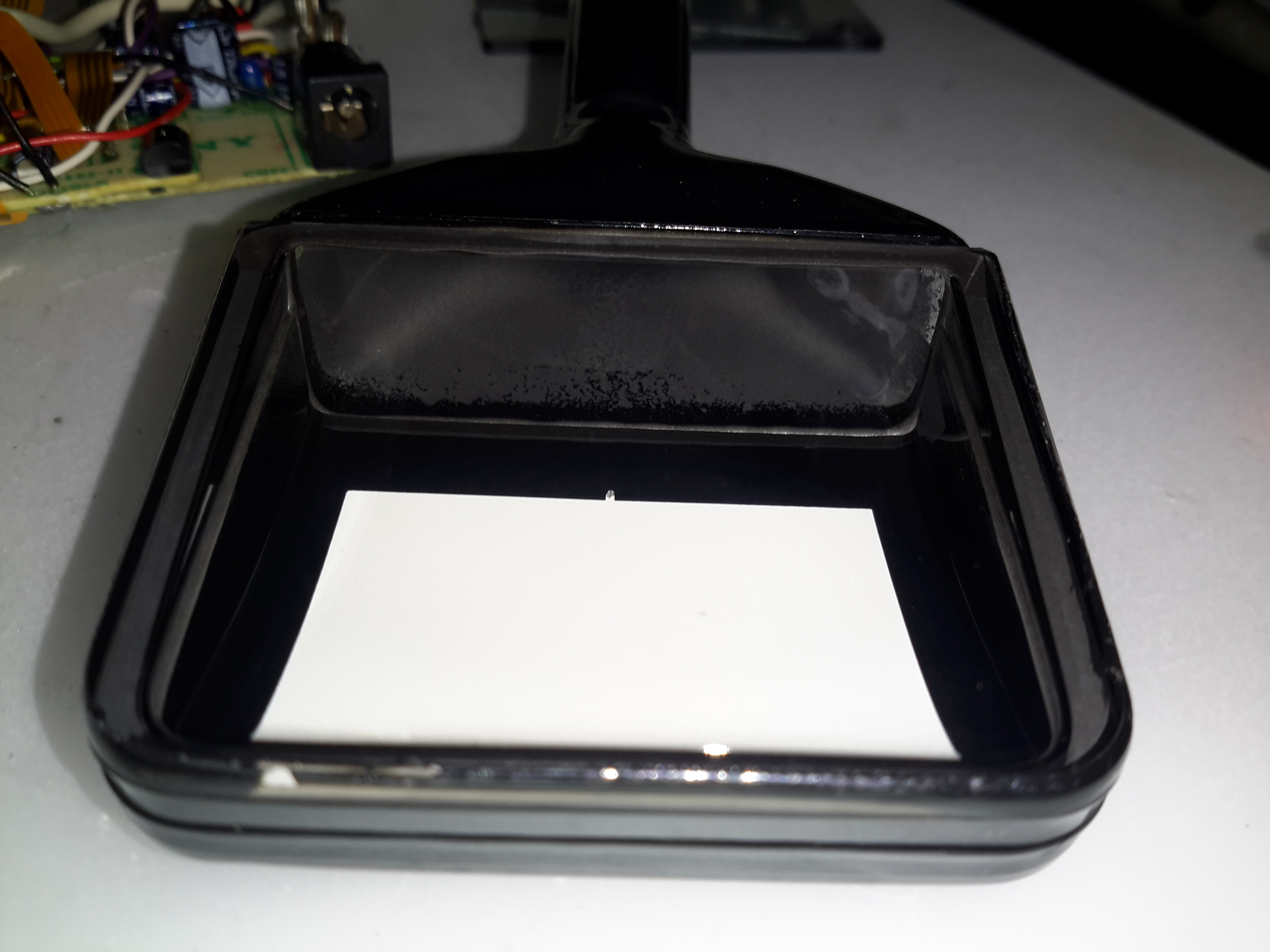
CRT Screen
Being a later model, this one has a much larger screen.
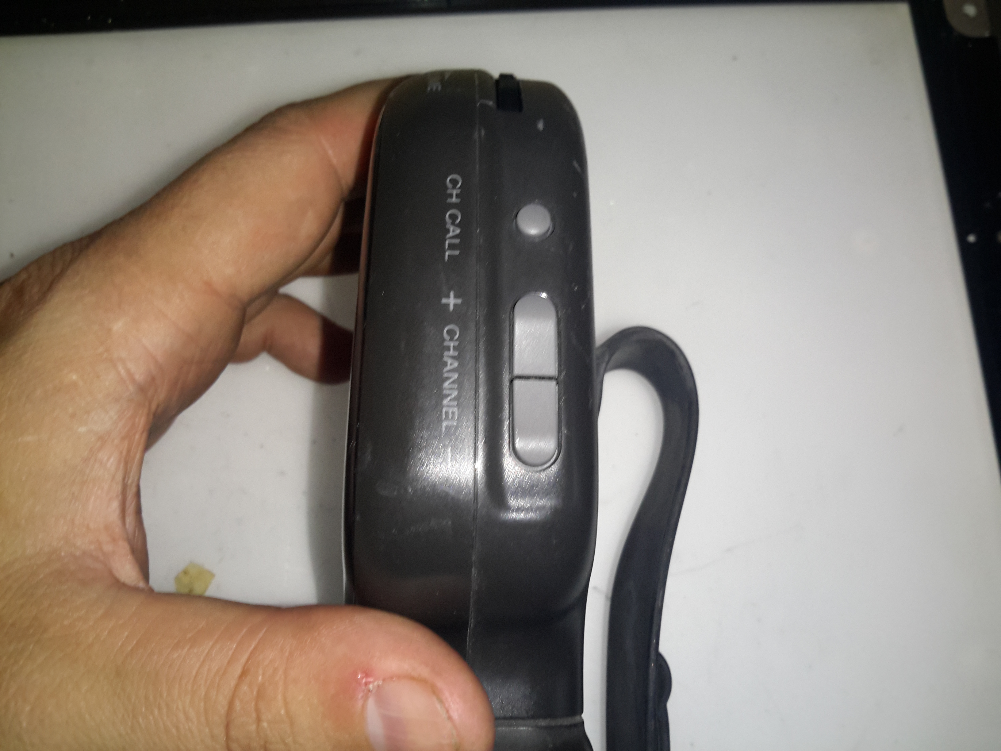
Autotuning
Instead of the manual tuner of the last Watchman, this one has automatic tuning control, to find the local stations.
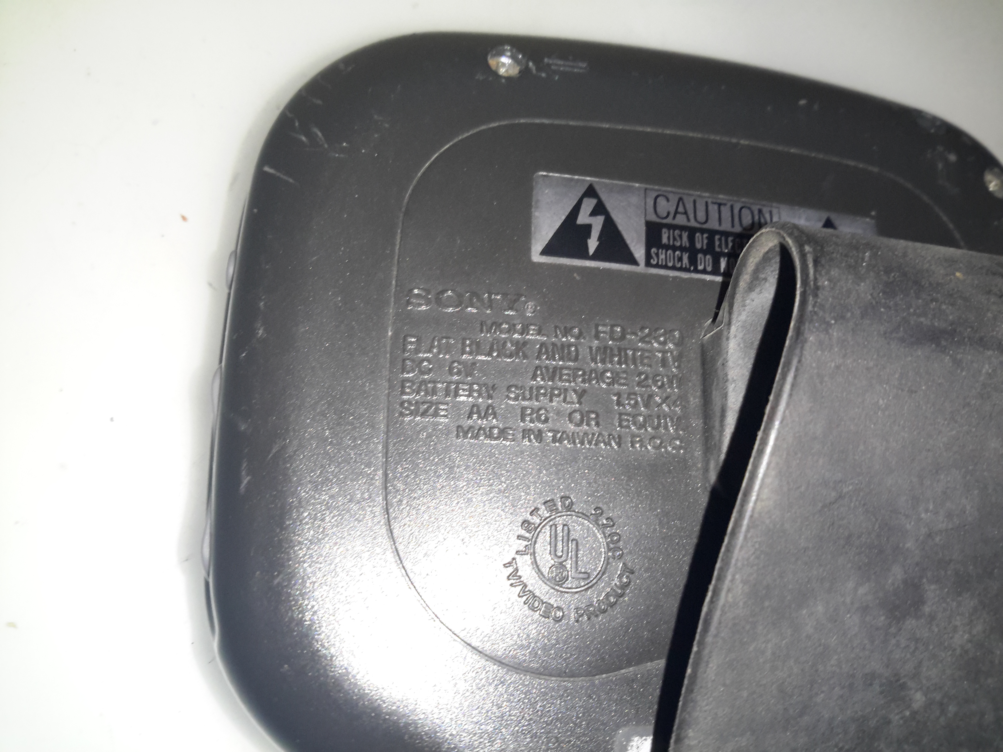
Spec Label
The spec puts the power consumption a little higher than the older TV, this isn’t surprising as the CRT screen is bigger & will require higher voltages on the electrodes.
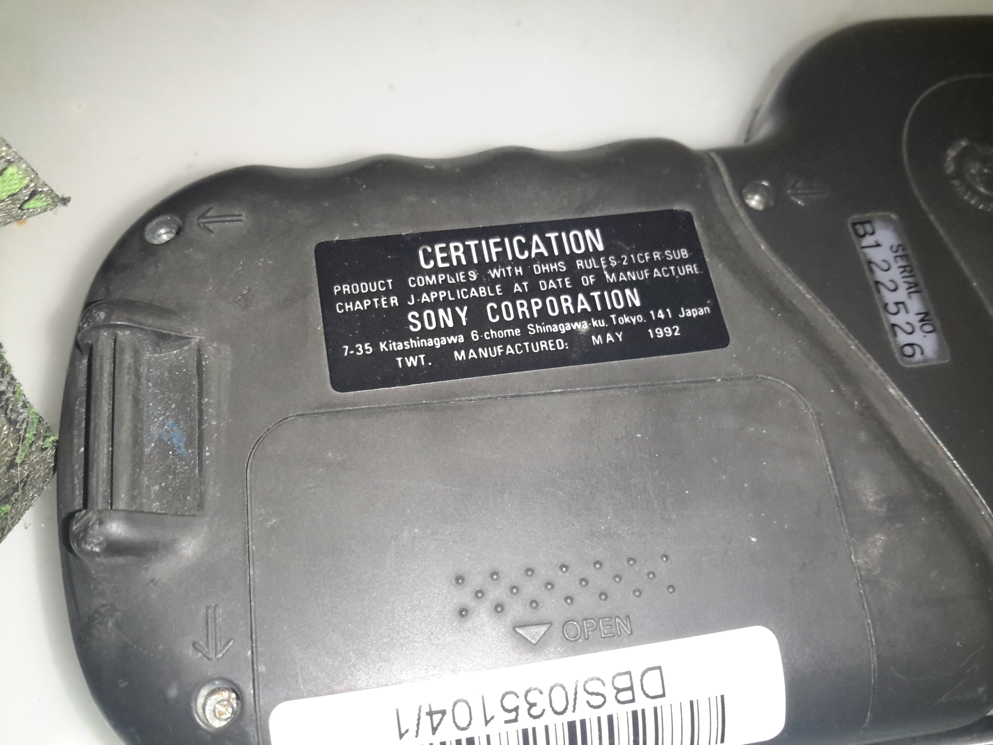
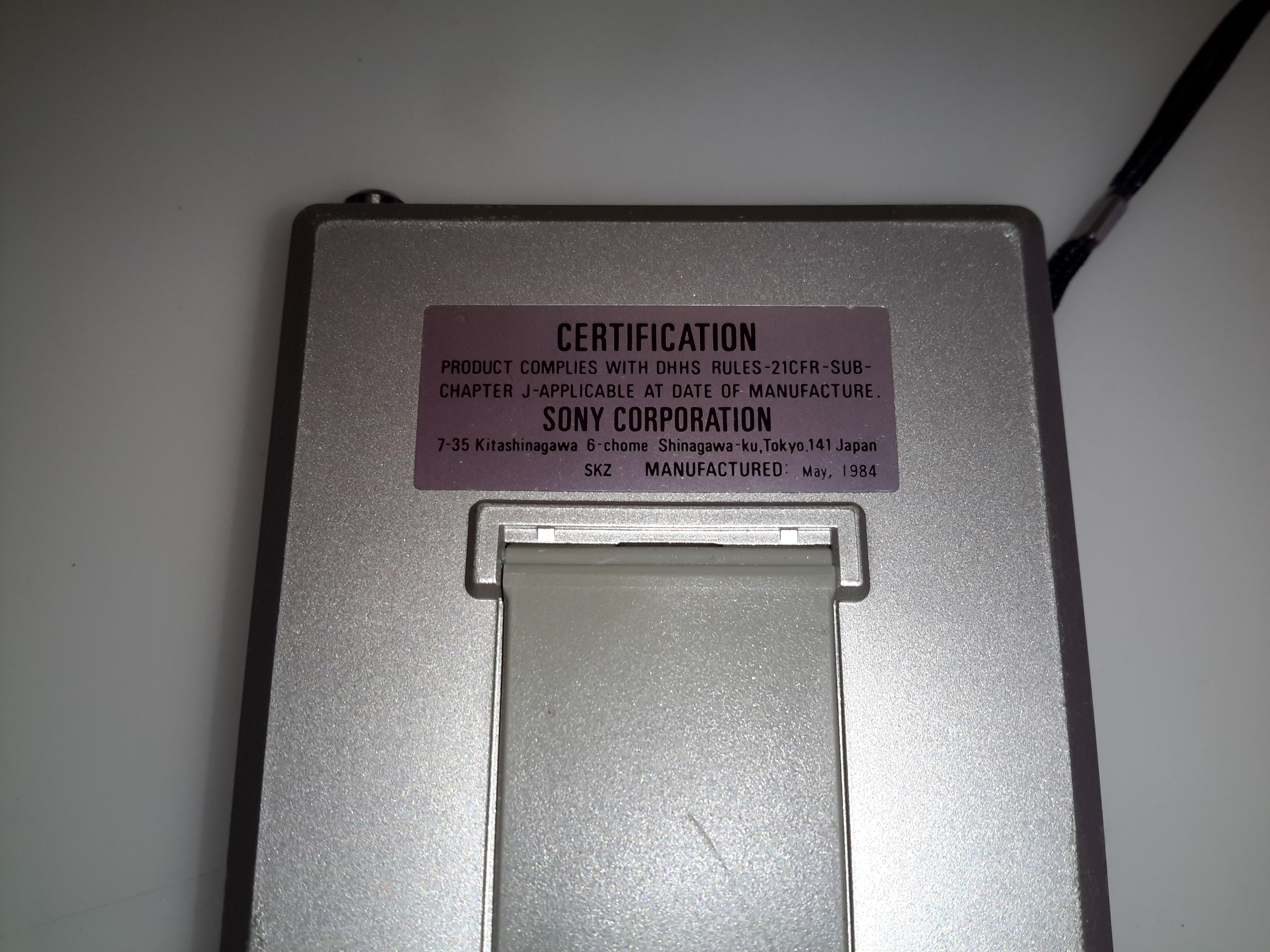
Certification Label
The certification label dates this model to May 1992.
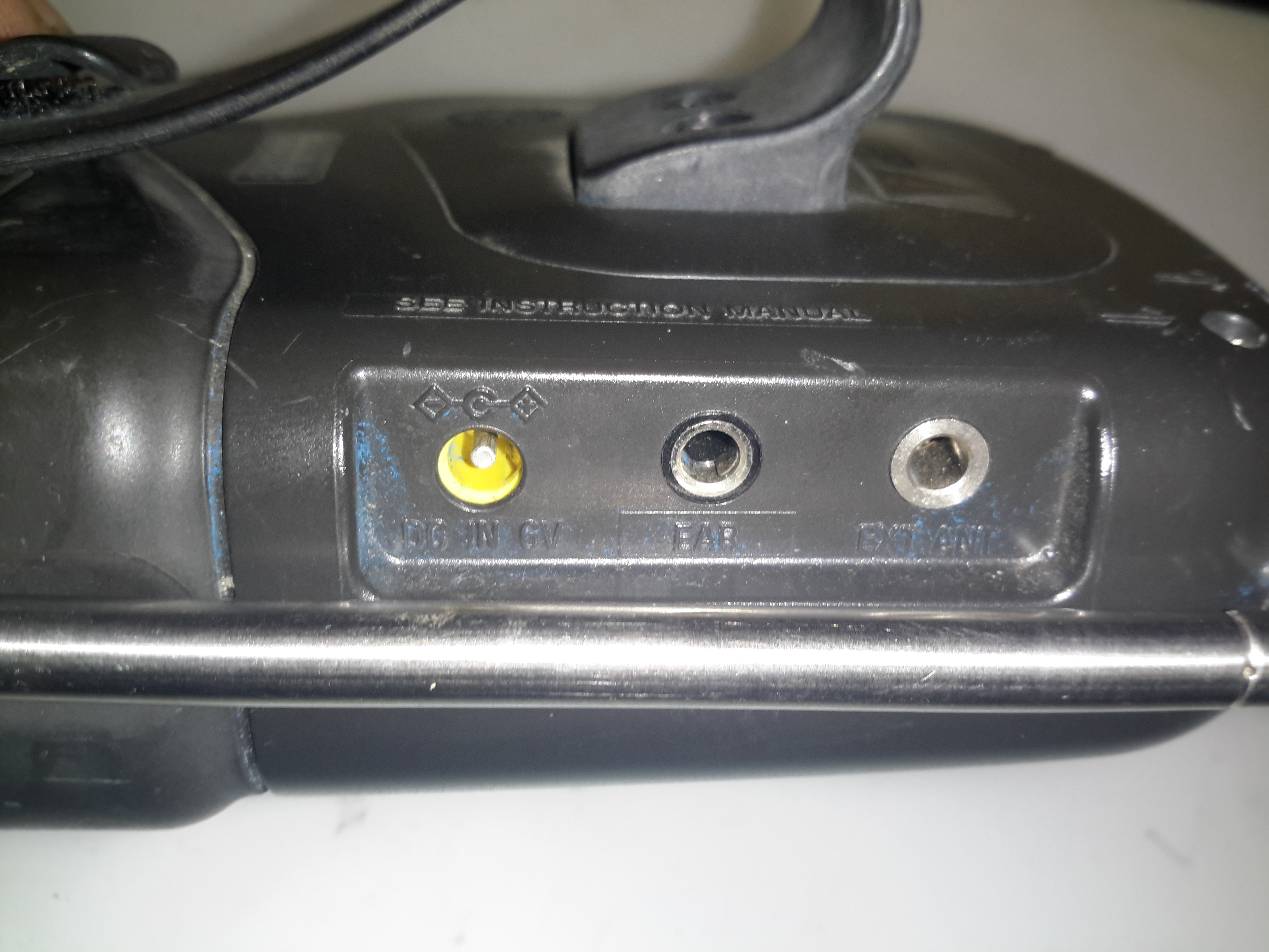
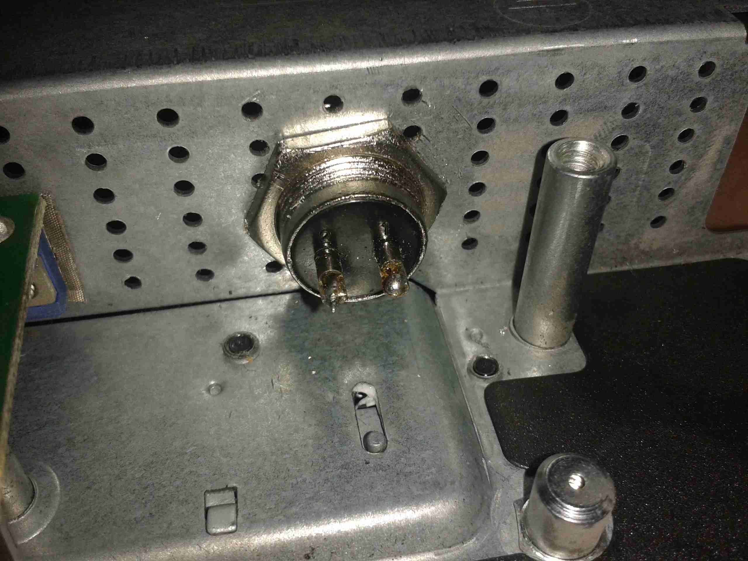
External Inputs
Still not much in the way of inputs on this TV. There’s an external power input, external antenna input & a headphone jack. No composite from the factory. (Hack incoming ;)).
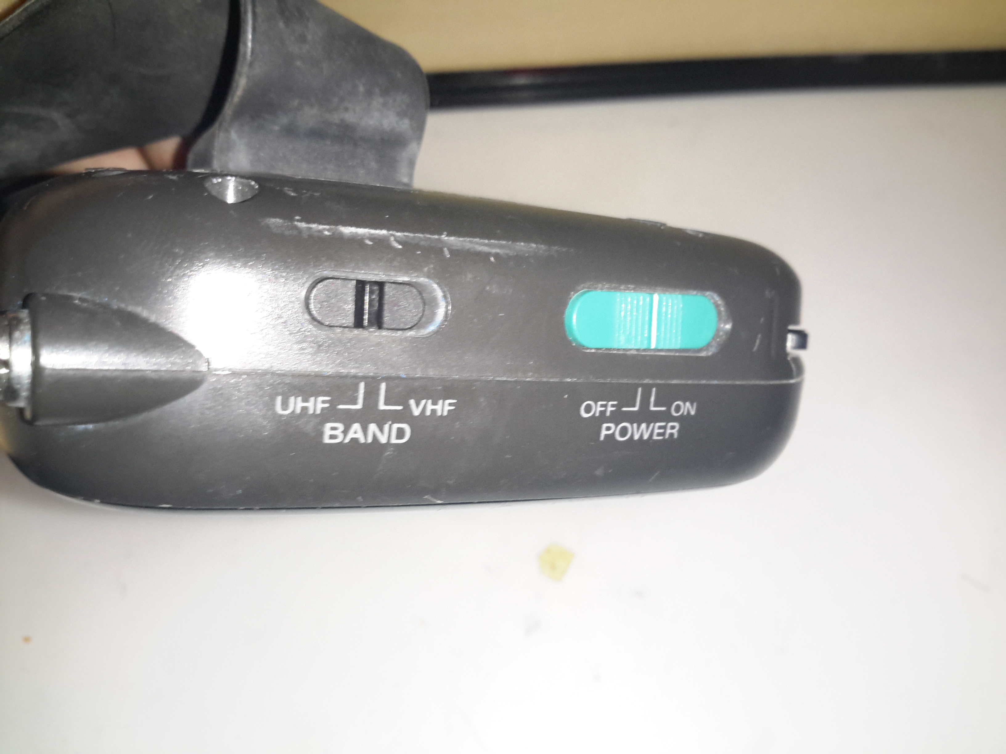
Power / Band
The UHF/VHF & power switches are on the top of this model.
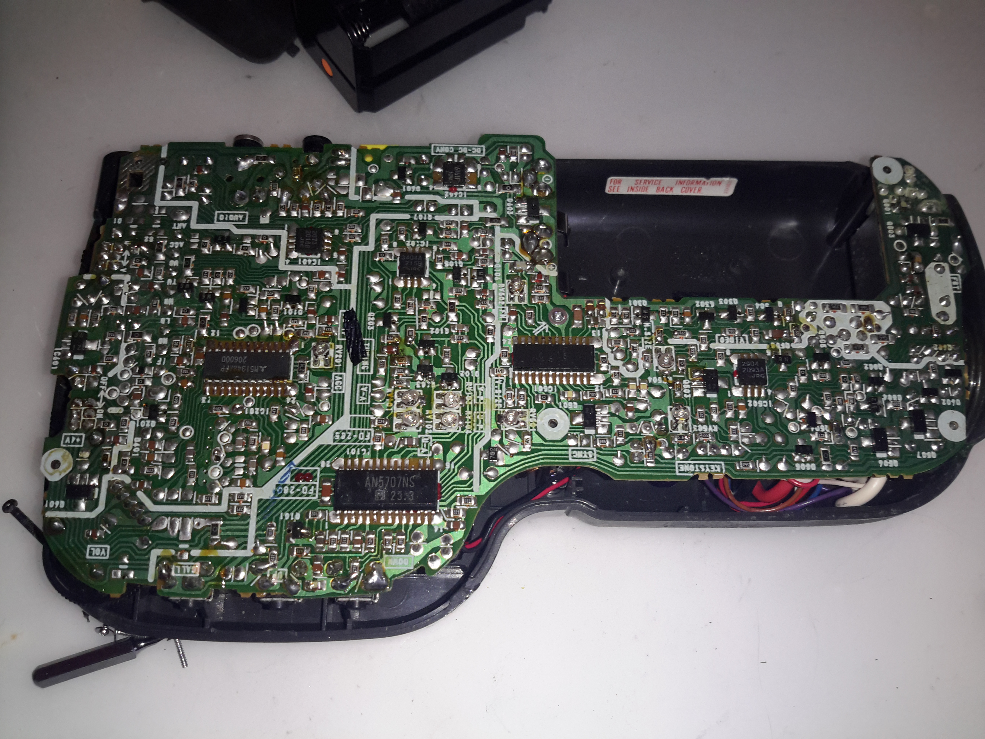
Back Cover Removed
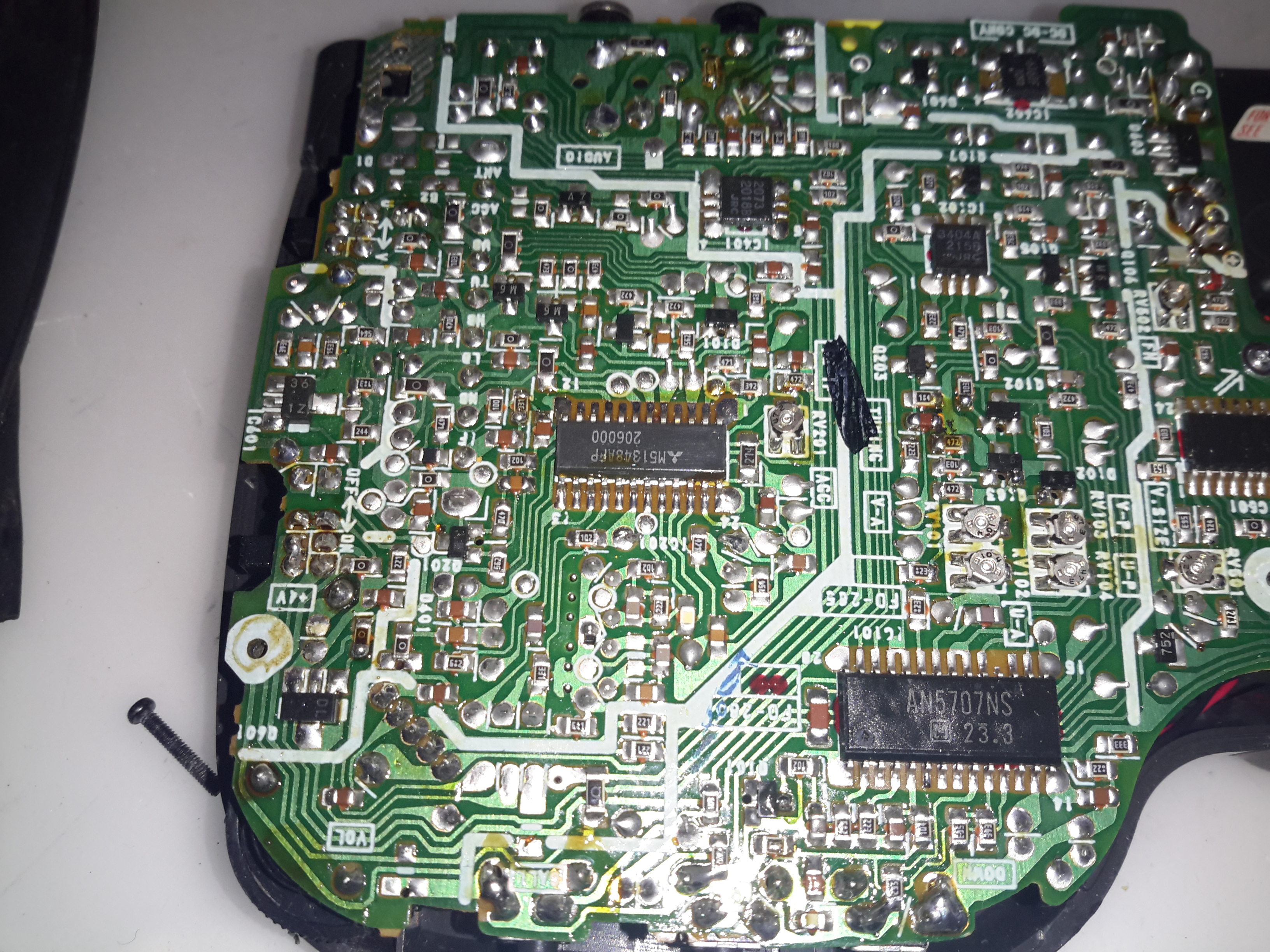
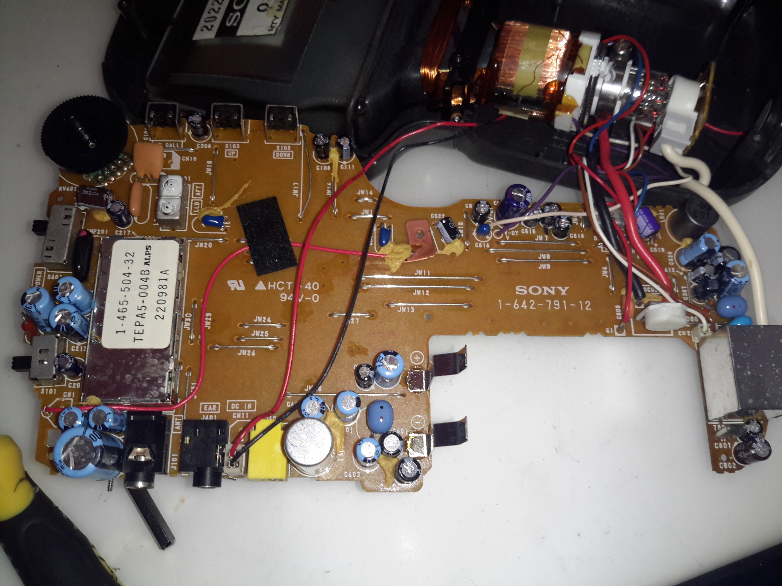
Removing some very tiny screws allows the back to be removed. There’s significant difference in this model to the last, more of the electronics are integrated into ICs, nearly everything is SMD.
RF Section
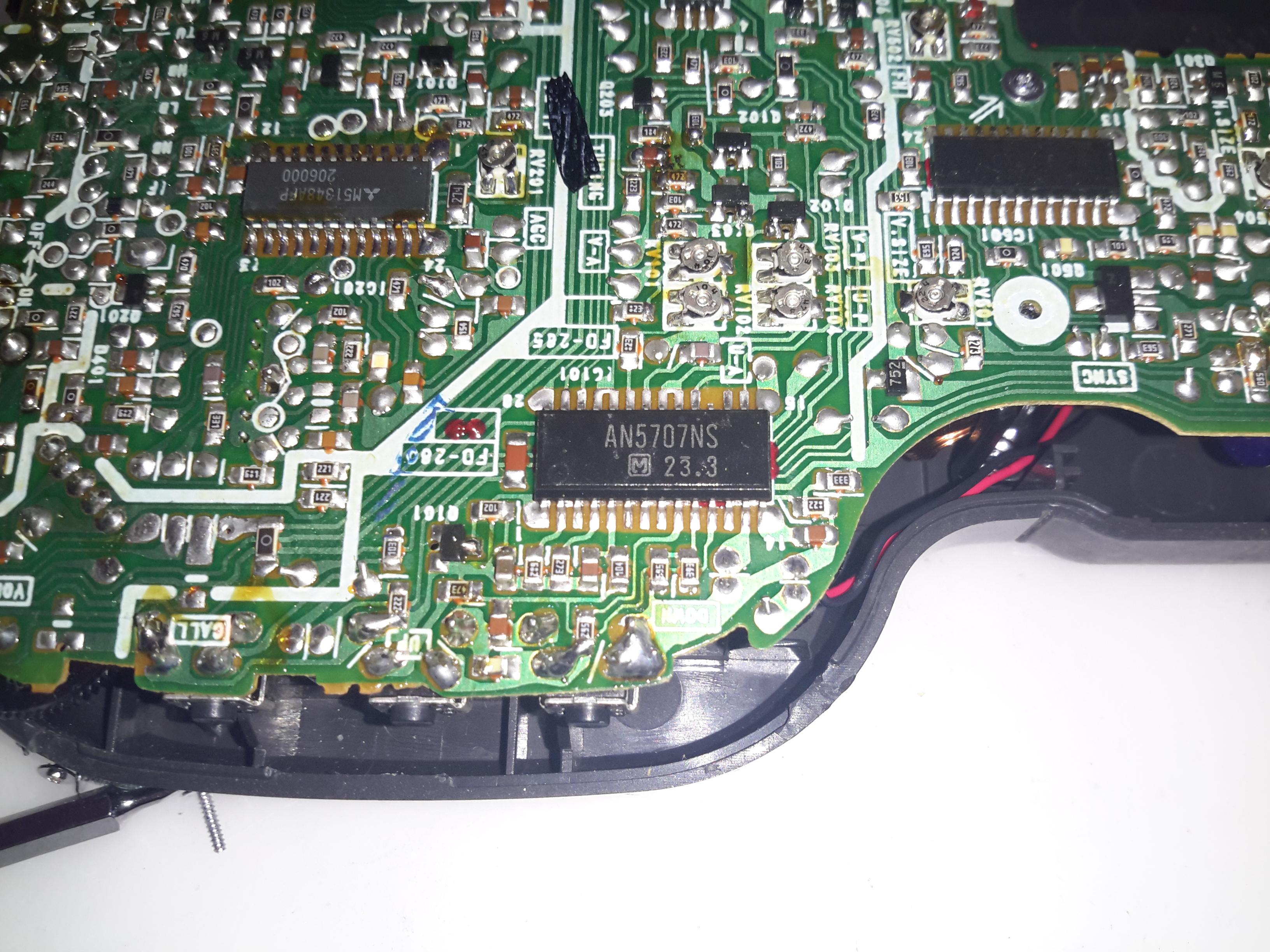
There’s the usual RF tuner section & IF, in this case the VIF/SIF is a Mitsubishi M51348AFP.
Tuner Controller
The digital control of the tuner is perfomed by this Panasonic AN5707NS.
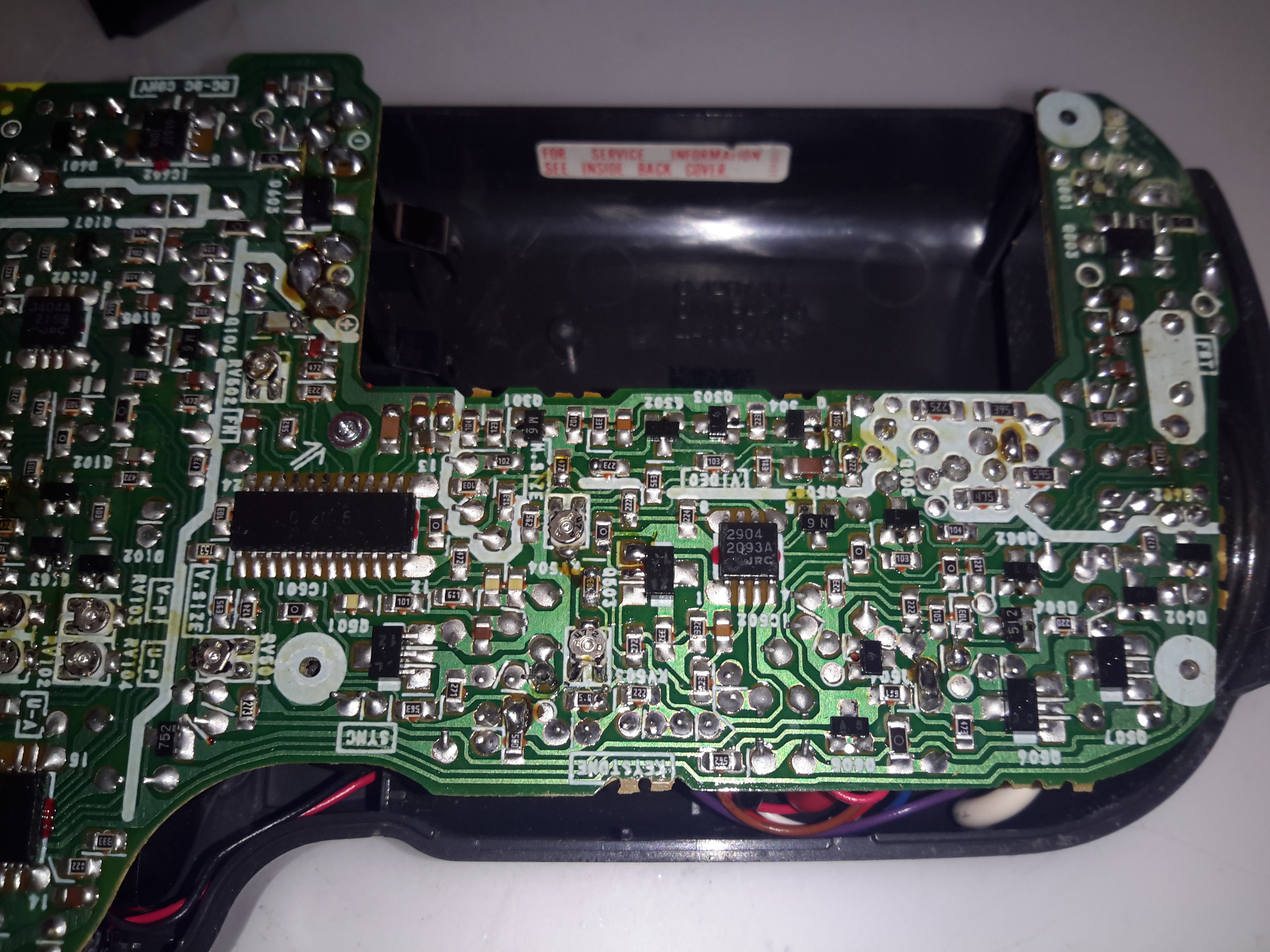
Deflection / Sync
The deflection & sync functions appear to be controlled by a single Sony branded custom IC, the CX20157. Similar to many other custom Sony ICs, a datasheet for this wasn’t forthcoming.
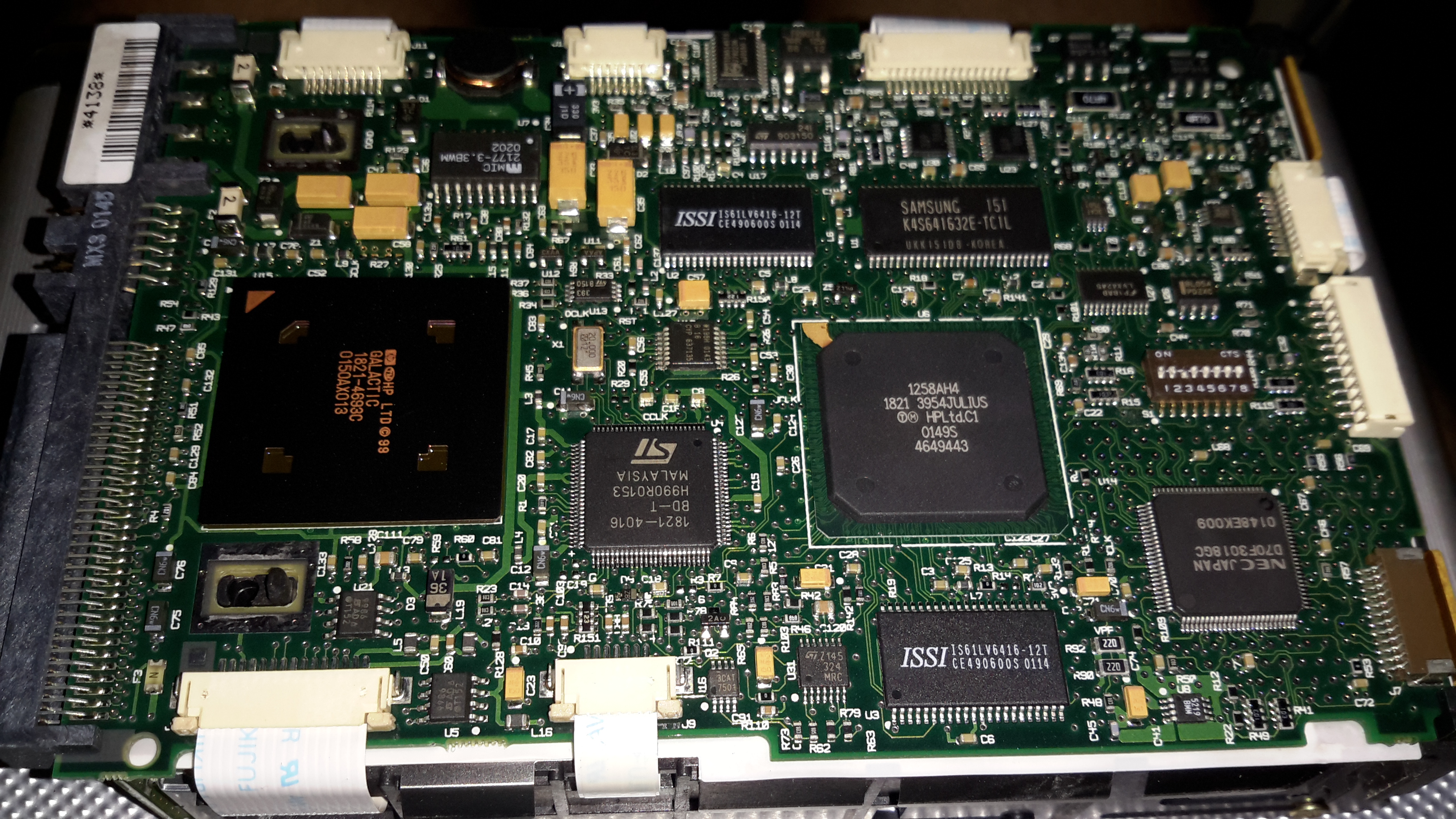
PCB Top
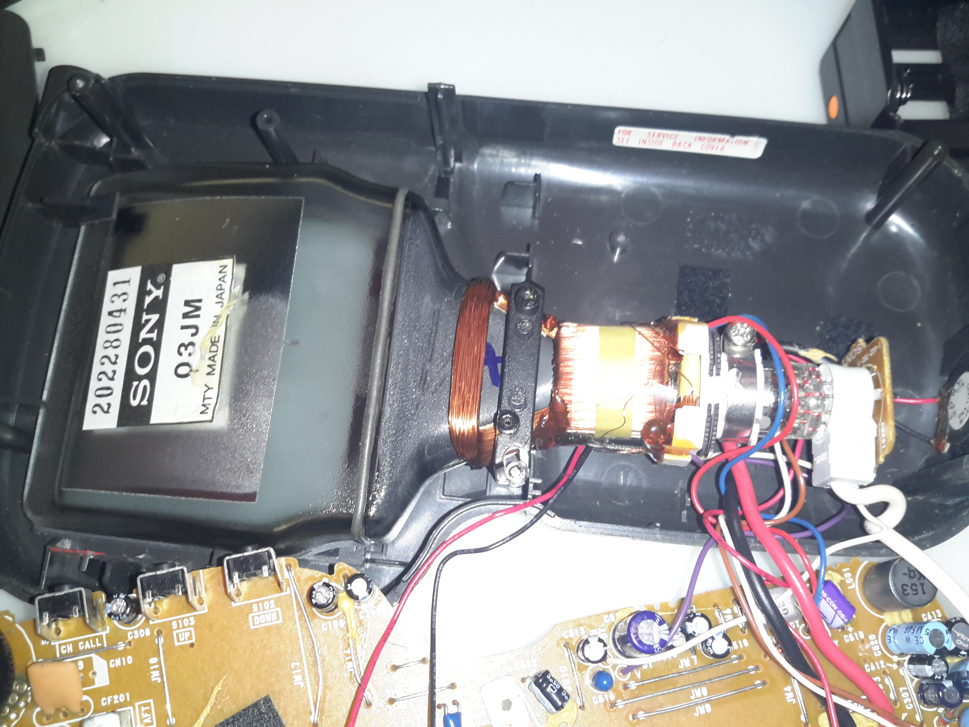
There’s very little on the top side of the board, the RF section is on the left, there’s a DC-DC converter bottom centre next to the battery contacts. This DC-DC converter has a very unusual inductor, completely encased in a metal can. This is probably done to prevent the magnetic field from interfering with the CRT.
CRT
Here’s the CRT itself, the Sony 03-JM. The back of this CRT is uncoated at the bottom, the tuning scale was taped to the back so it lined up with the tuning bar displayed on the screen.
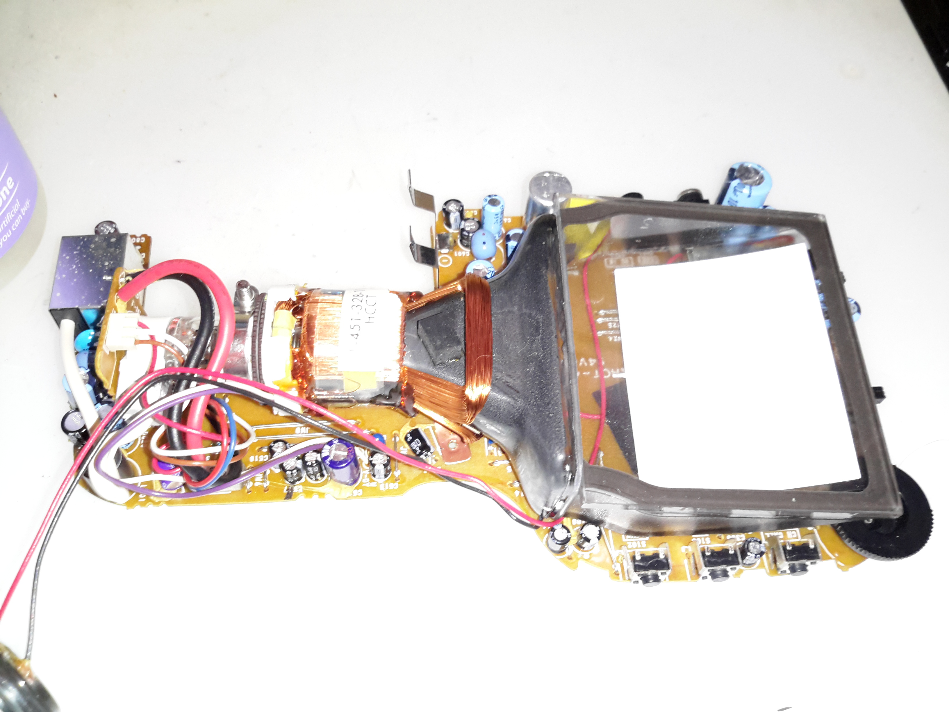
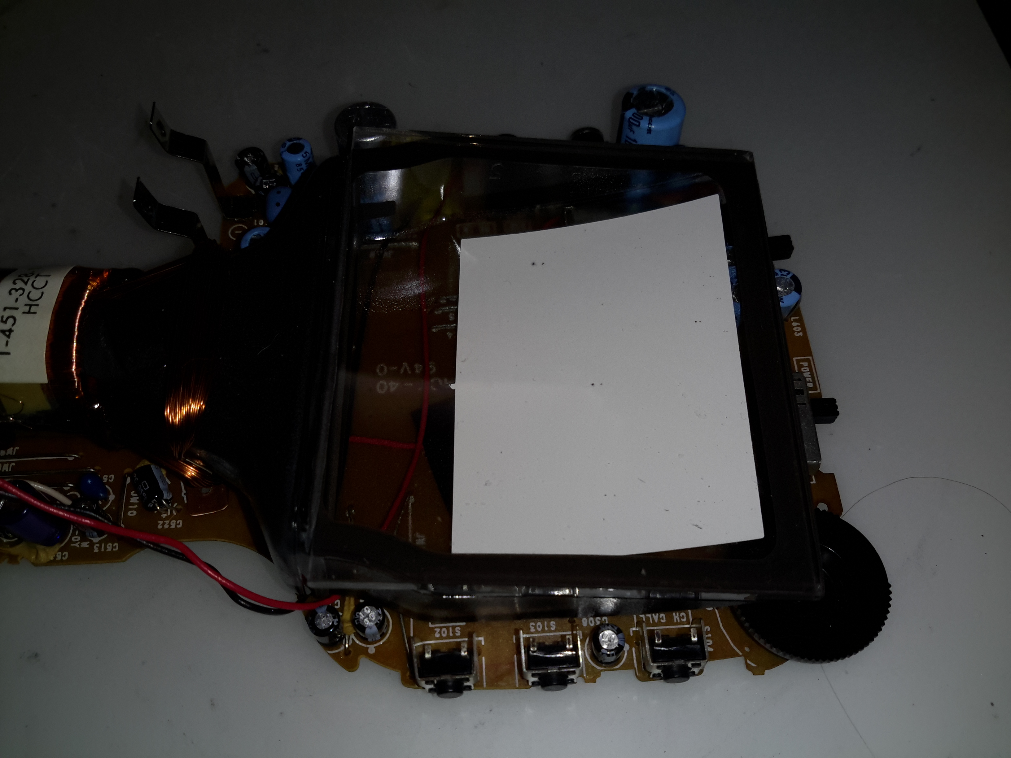
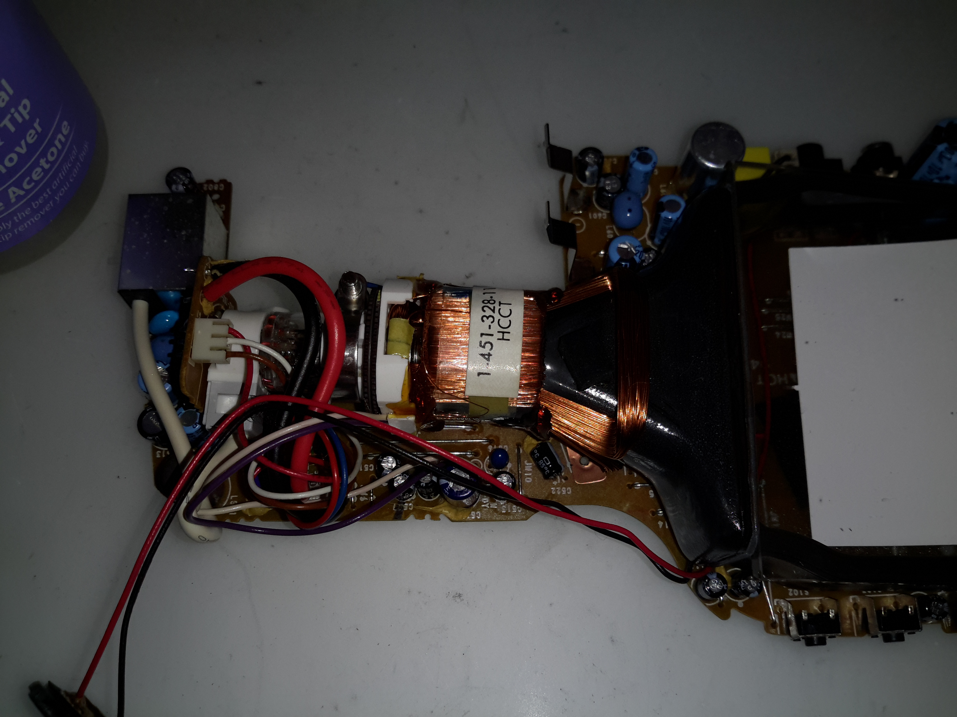
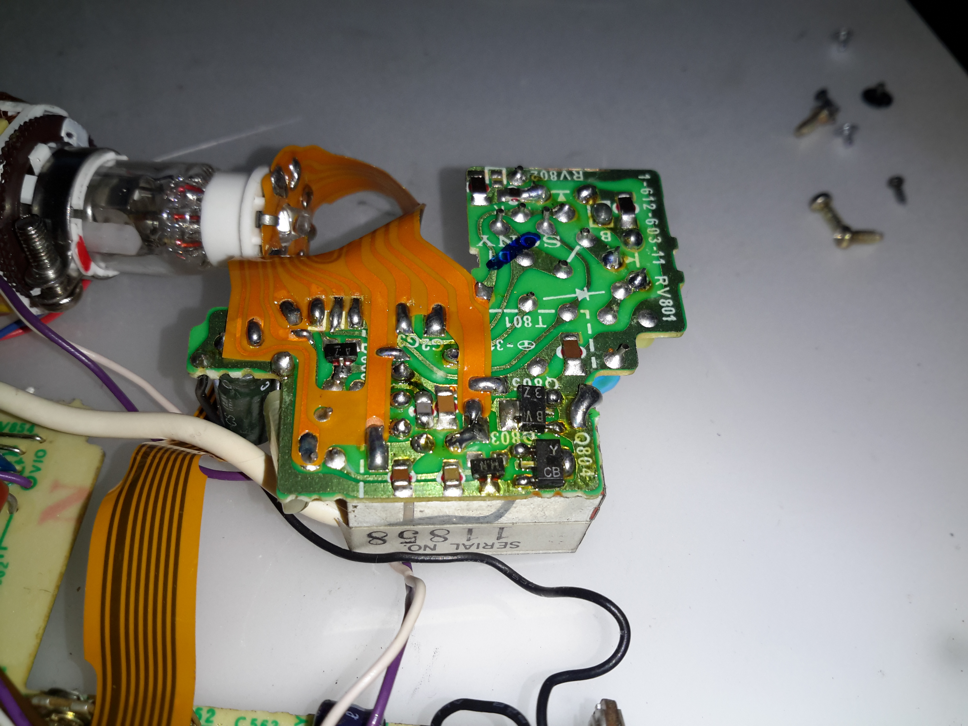
Electronics
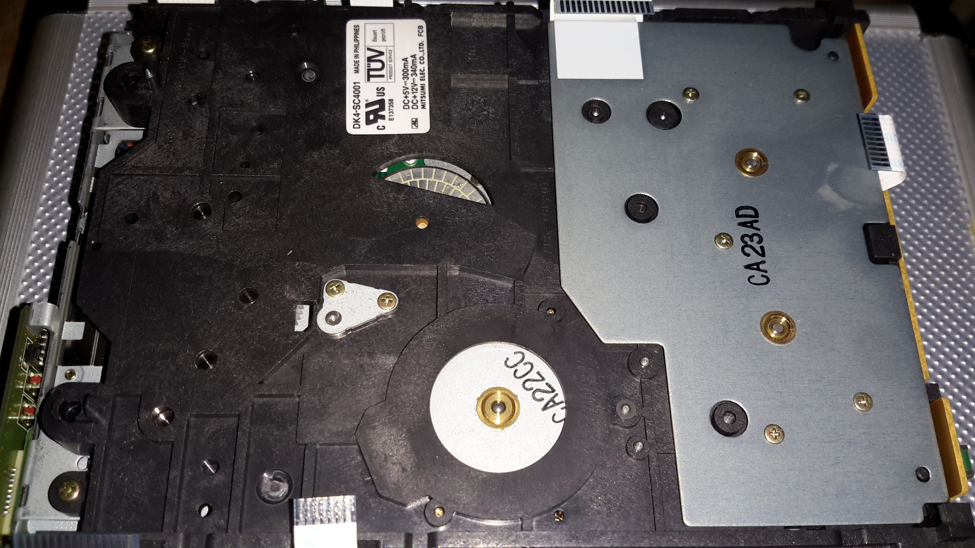
Here’s the electronics completely removed from the shell. There’s much more integration in this model, everything is on a single PCB.
Phosphor Screen
The curve in the phosphor screen can clearly be seen here. This CRT seems to have been cost-reduced as well, with the rough edges on the glass components having been left unfinished.
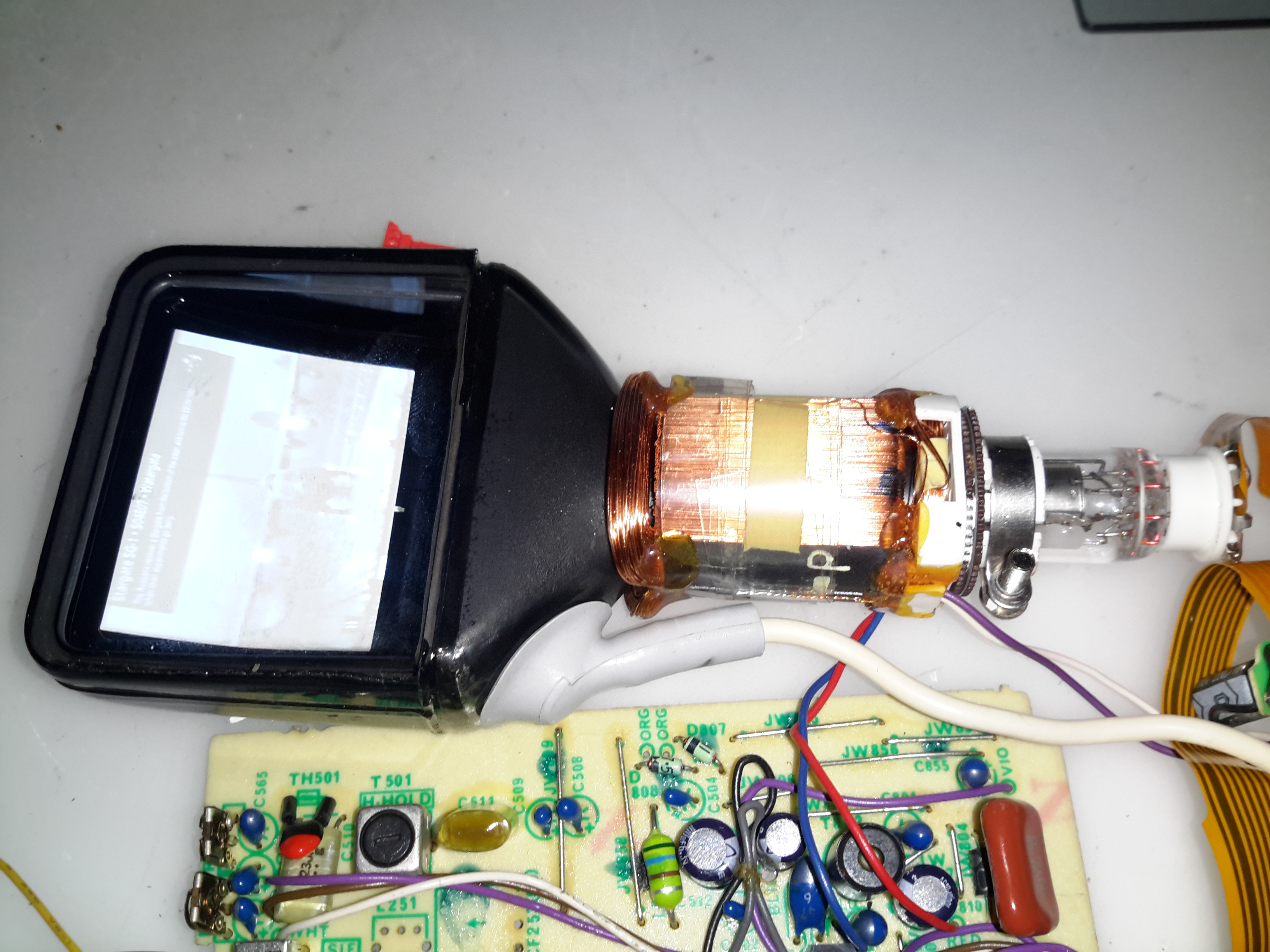
Electron Gun
Here’s the electron gun end of the tube. There isn’t a separate final anode connection to the bell of the tube unlike the previous model. Instead the final anode voltage is on a pin of the electron gun itself. This keeps all the wiring to the tube at one end & shortens the high voltage cable.
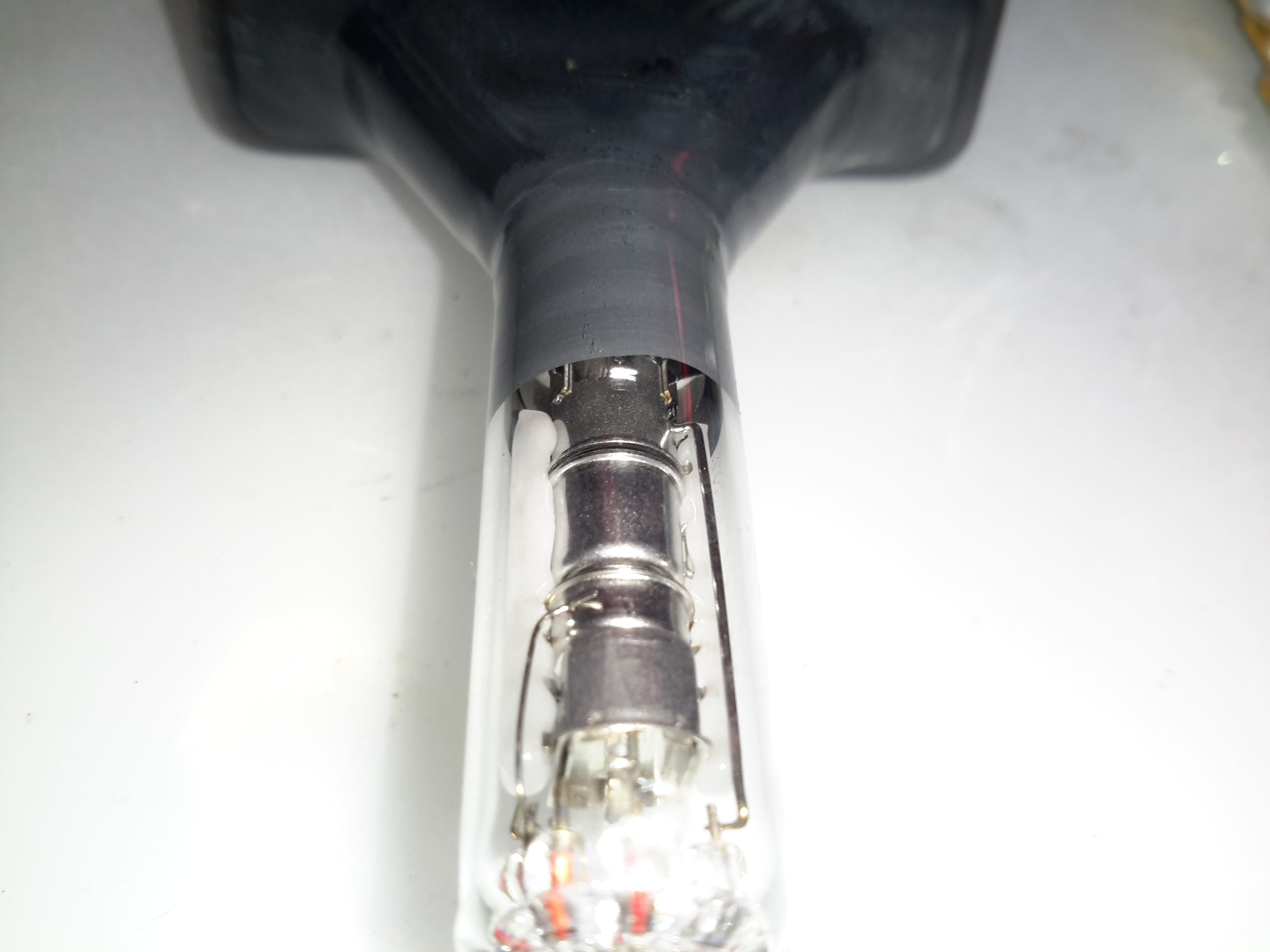
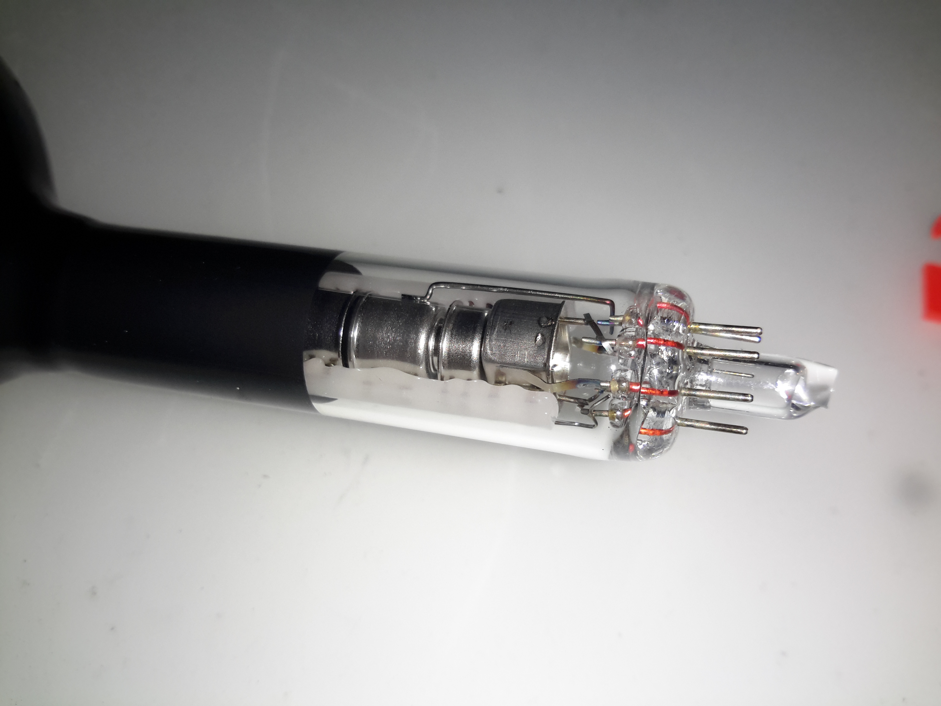
Electron Gun
Here’s the gun in the neck of the tube. Again this is pretty much standard fare for CRT guns. It’s more similar to a viewfinder tube in that the anode connection is running from the pins at the back. (It’s the line running up the right side of the tube). I’m guessing the anode voltage is pretty low for this to work without the HV flashing over, probably in the 2-4kV range.
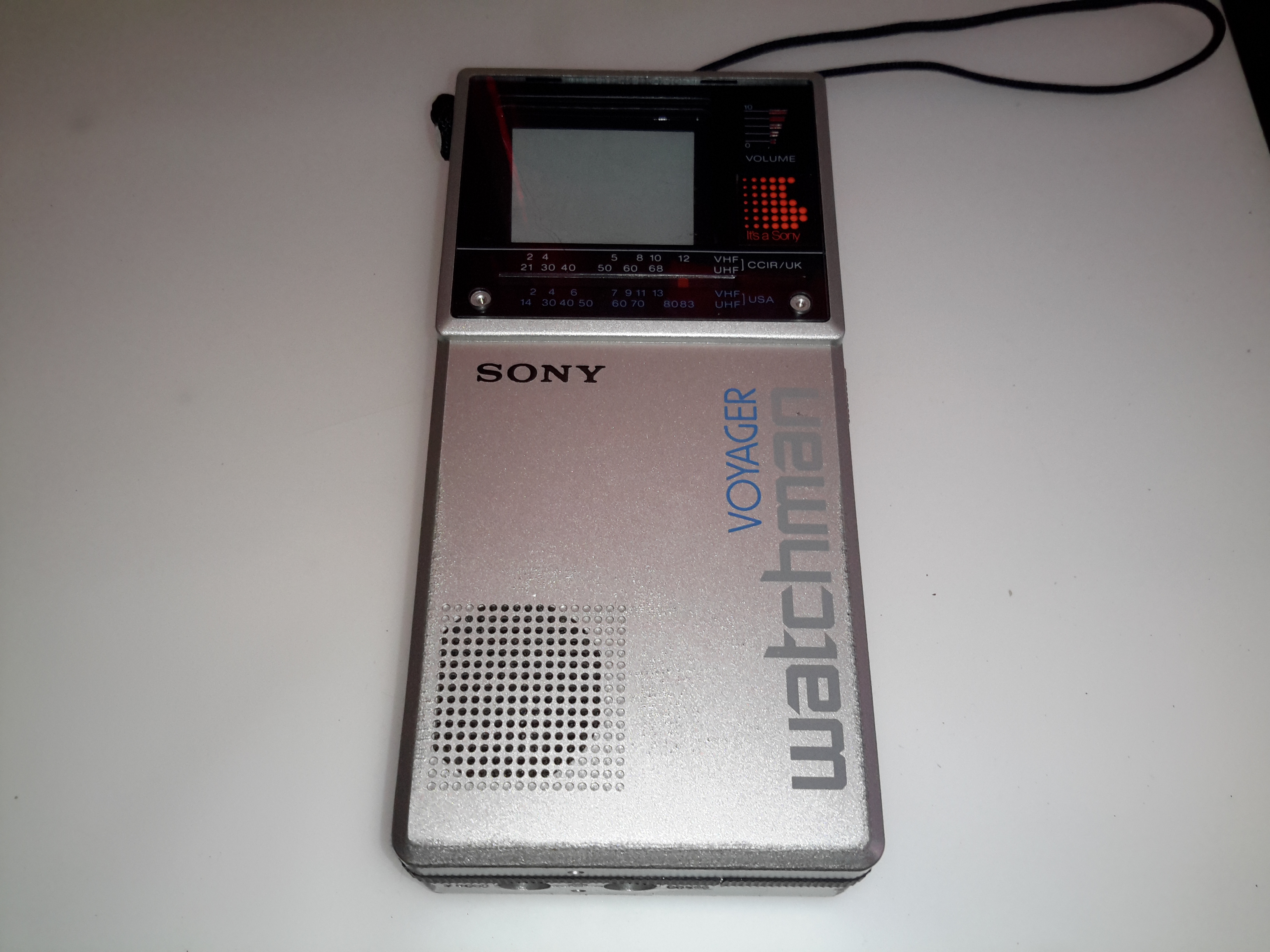
Here’s an oddity from the 1980’s – a CRT-based portable TV, with a very strangely shaped tube. Sony produced many types of flat CRTs back in the 80’s, with the electron gun at 90° to the curved phosphor screen.
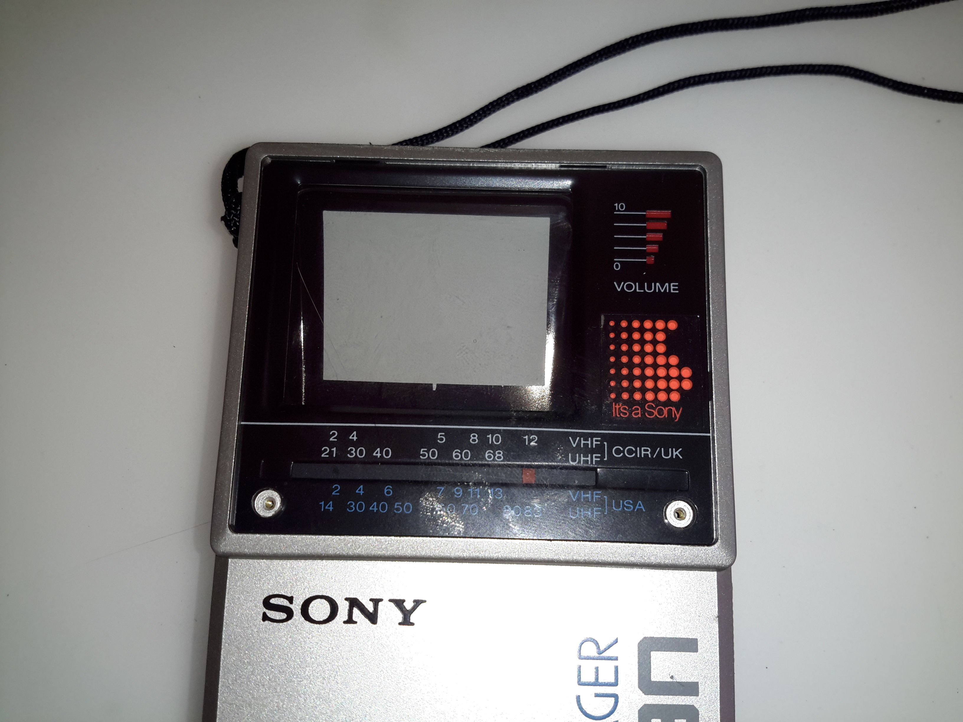
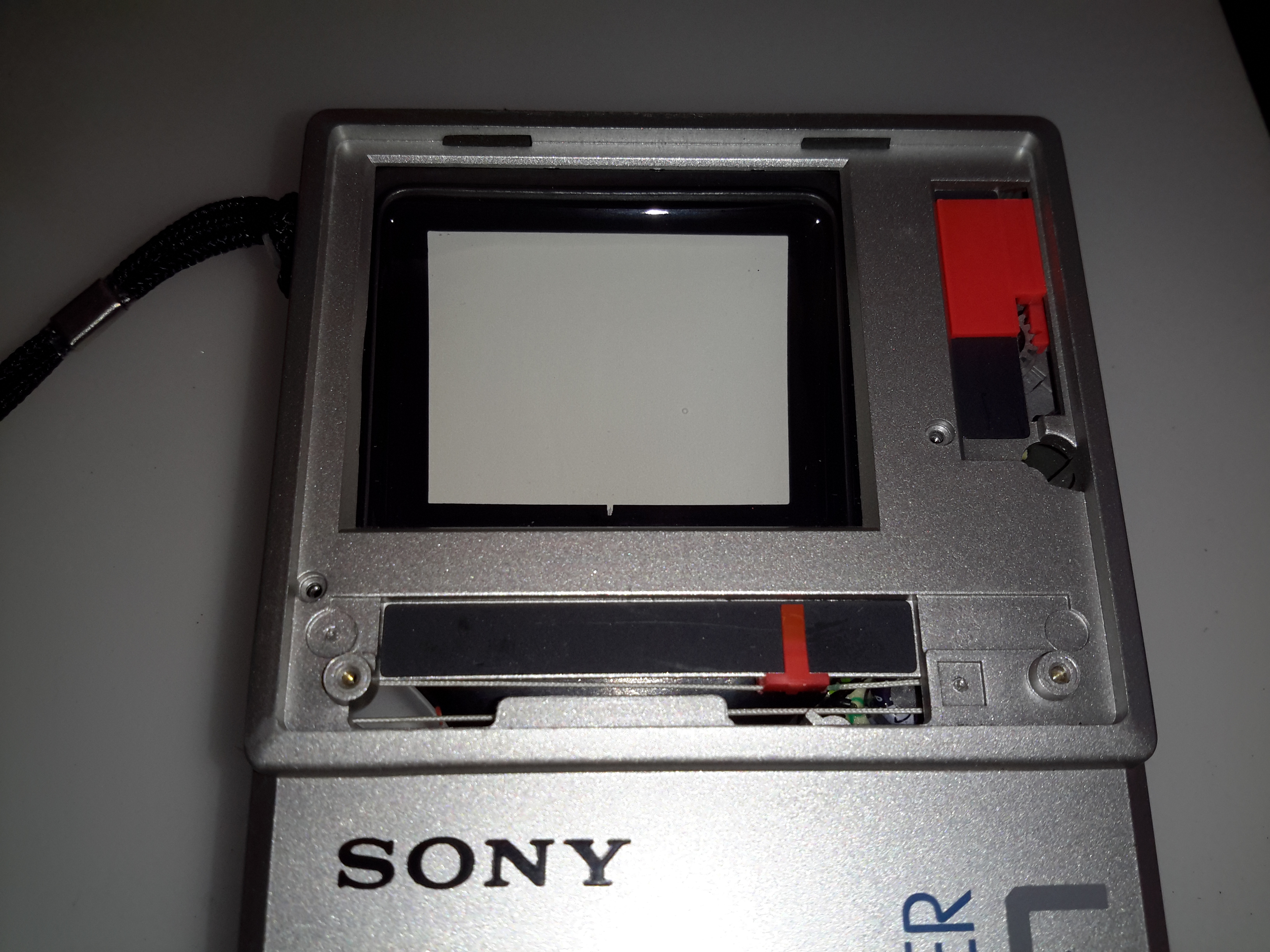
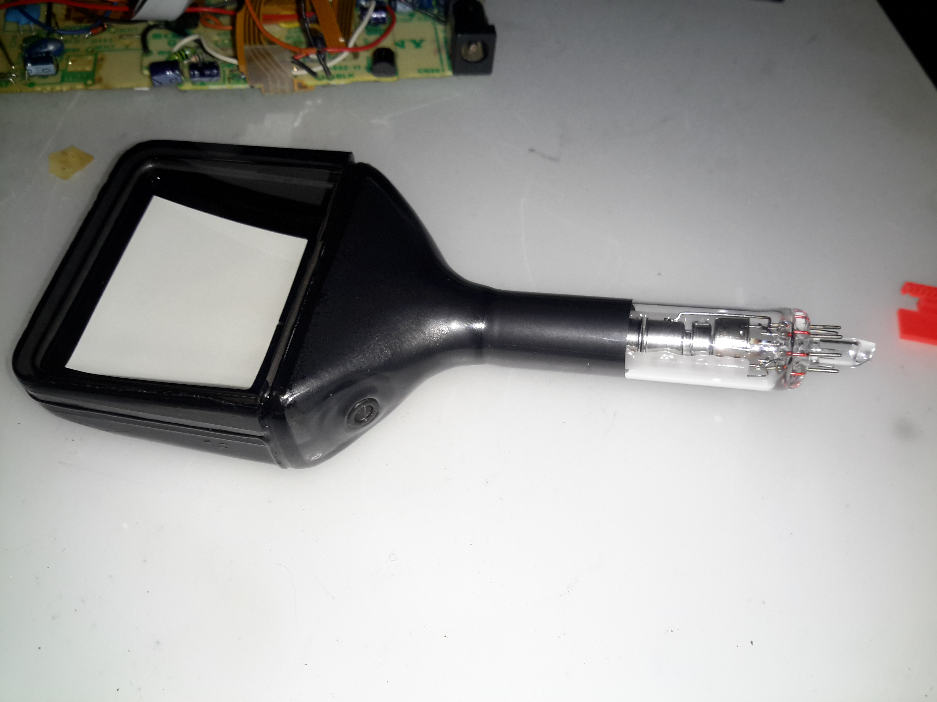
Front Panel
The front panel has the display window, along with the tuning & volume indicators. Unfortunately since analogue TV transmissions have long been switched off, this unit no longer picks up any transmissions off the air, but it can be modified to accept a composite video input.
Back Panel
The back panel has the battery compartment & the tilt stand.
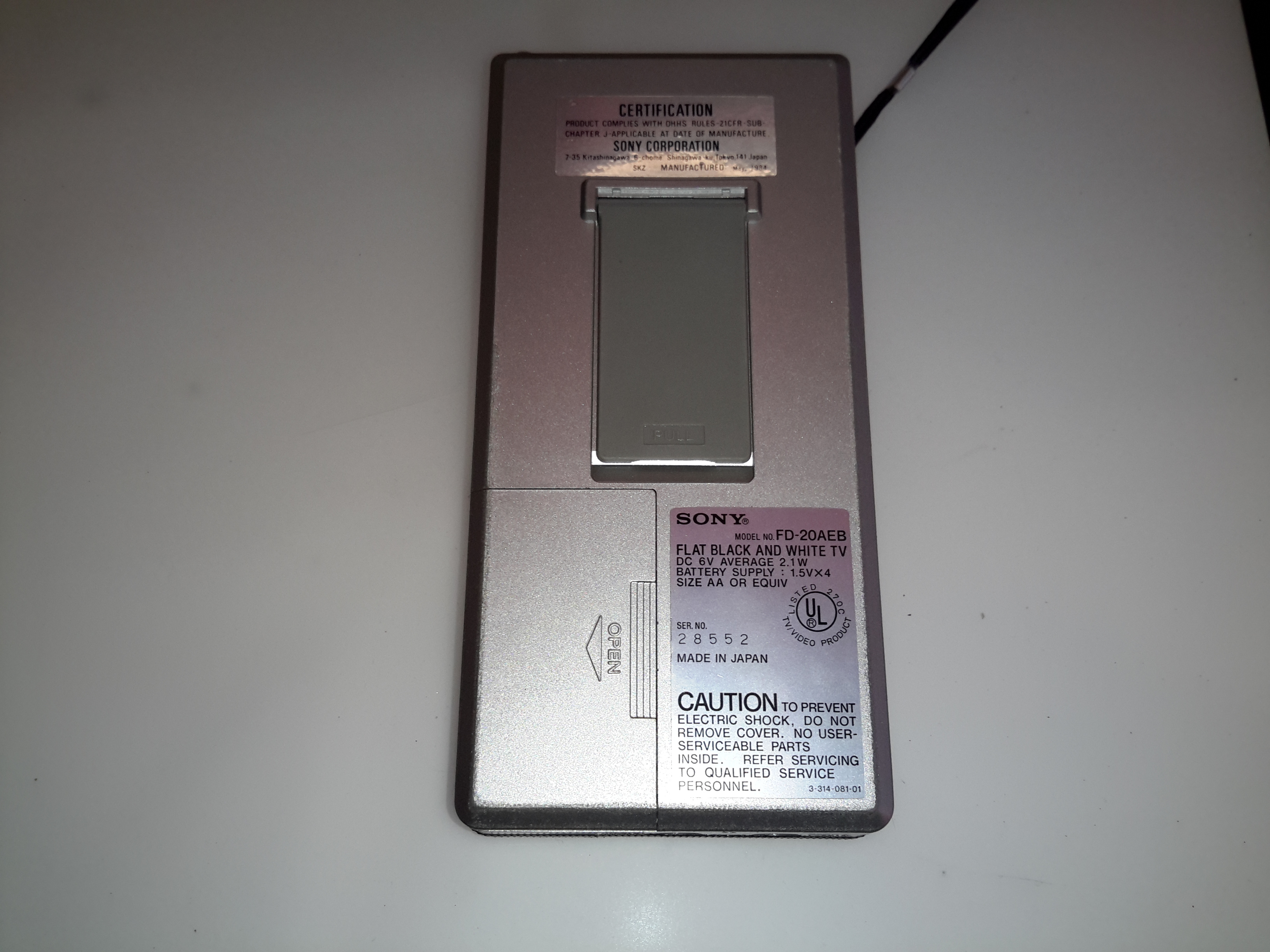
Certification
The certification label reveals this unit was manufactured in May 1984, 32 years ago!
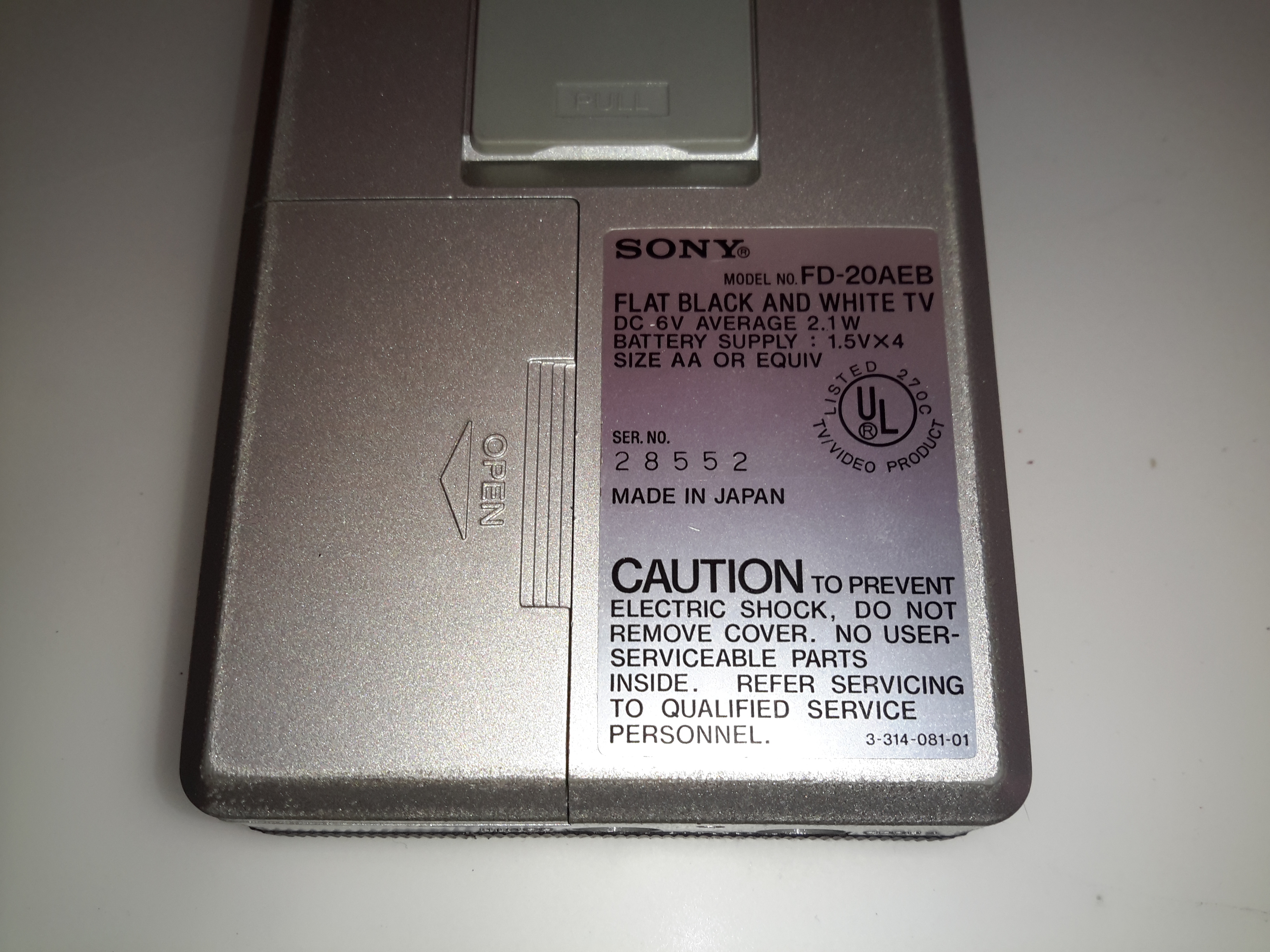
Spec. Label
Rated at 6v, ~2.1W this device uses surprisingly little power for something CRT based.
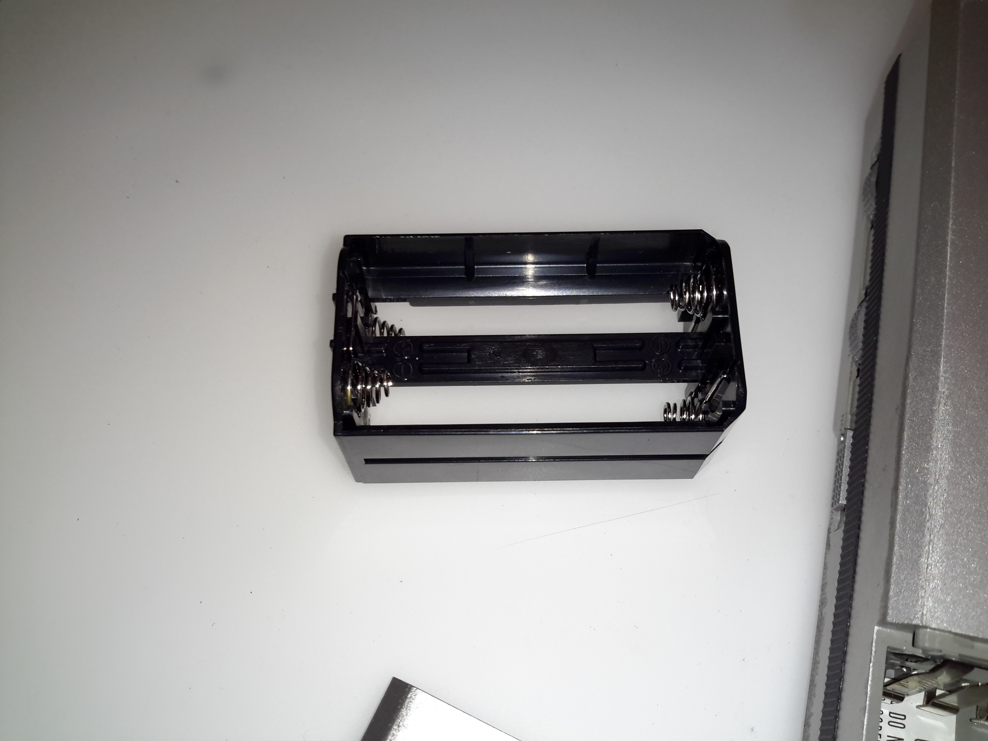
Battery Holder
The battery holder is a little unique, this plastic frame holds 4 AA cells, for a 6v pack.
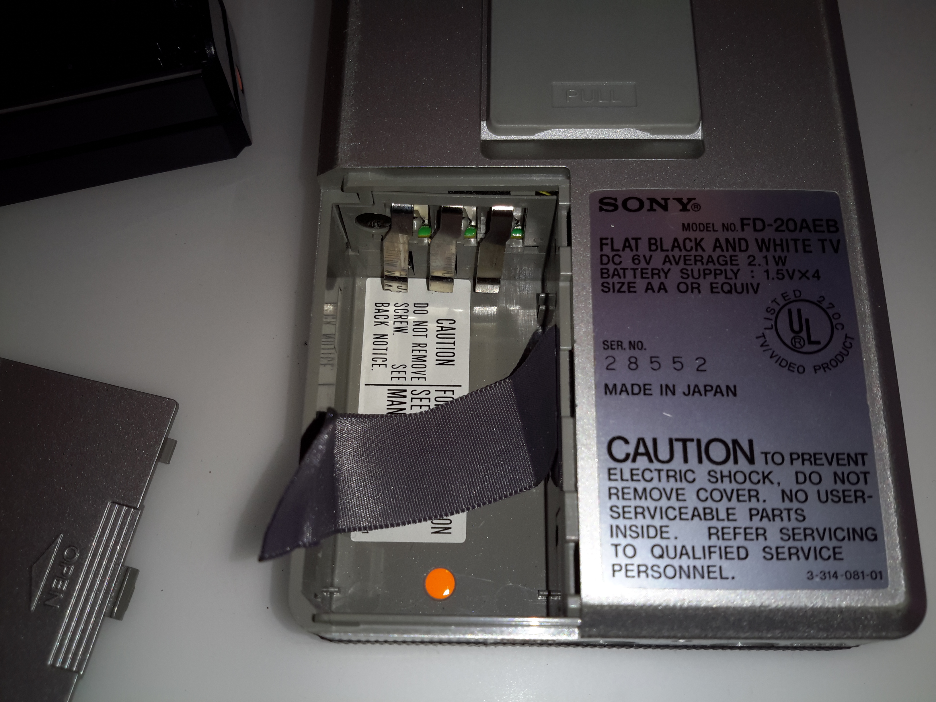
Battery Compartment
The battery holder slots into the back of the TV, there’s also an extra contact that the service manual mentions is for charging, so I assume a rechargeable 6v battery pack was also available.
Front Panel Removed
Removing a pair of pin-spanner type screws allows the front glass & screen printed CRT surround to be removed. Not much more under here other than the pair of screws that retain the CRT in the front frame.
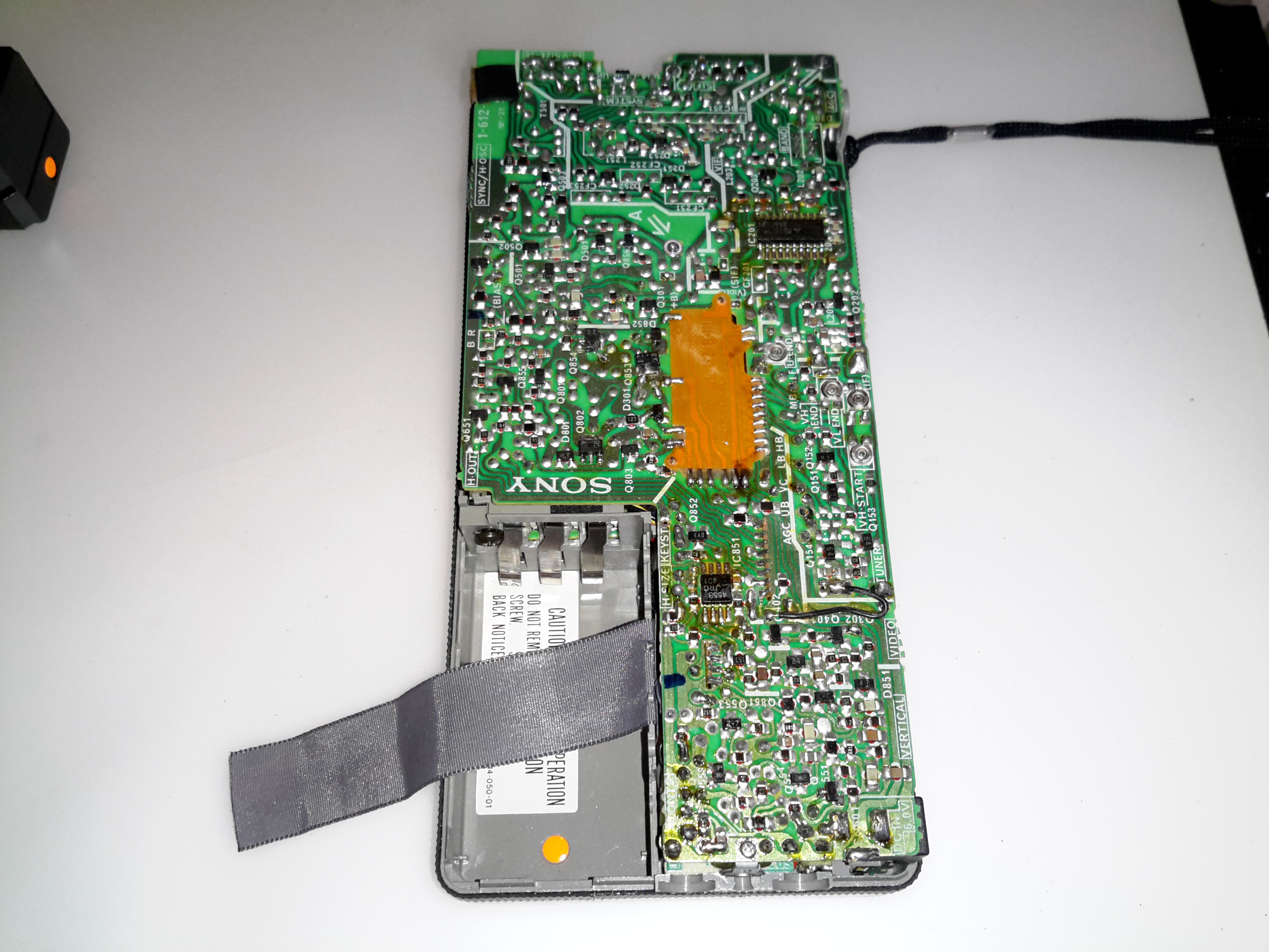
Back Cover Removed
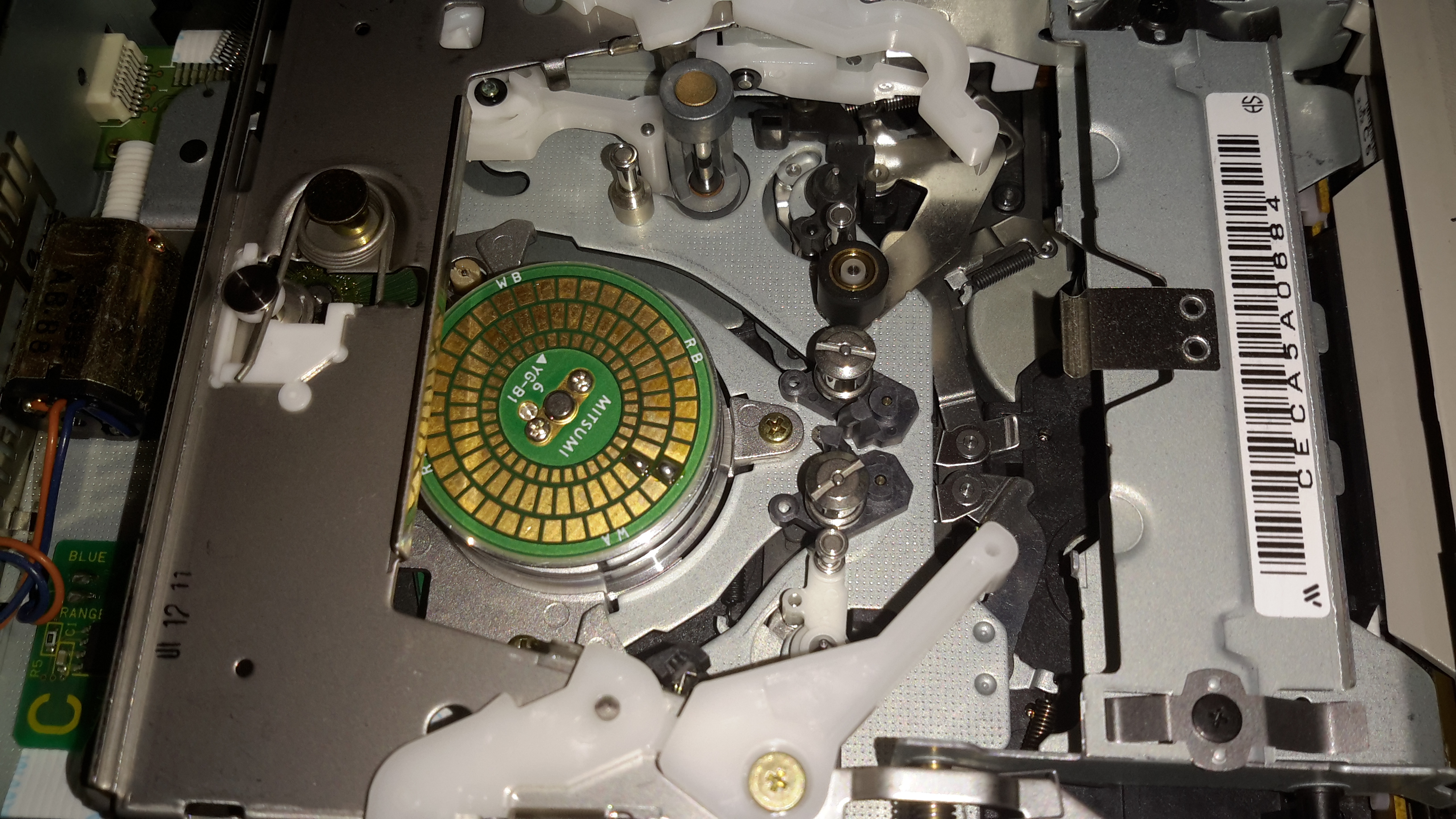
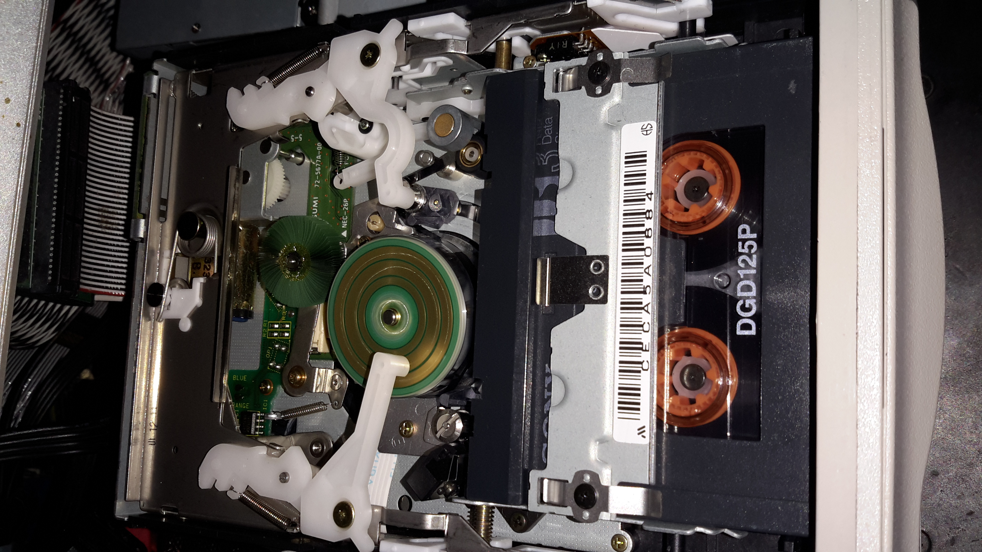
Here’s the back cover removed, after unscrewing some very small screws. As per usual with Sony gear, the electronics is extremely compacted, using many flat flex cables between the various PCBs. The main PCB is visible at the back, this has all the deflection circuitry, RF tuner, Video IF, Audio IF, video amplifier & composite circuitry.
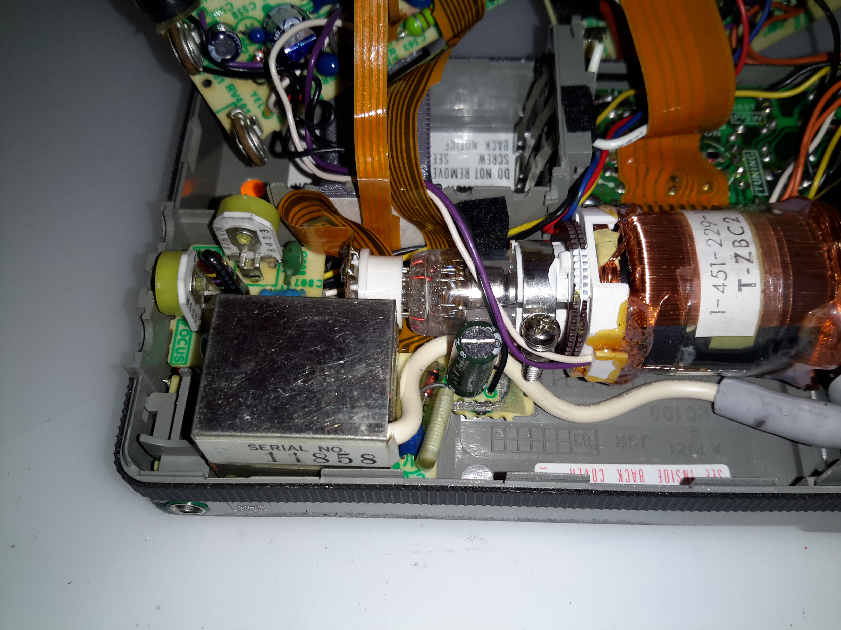
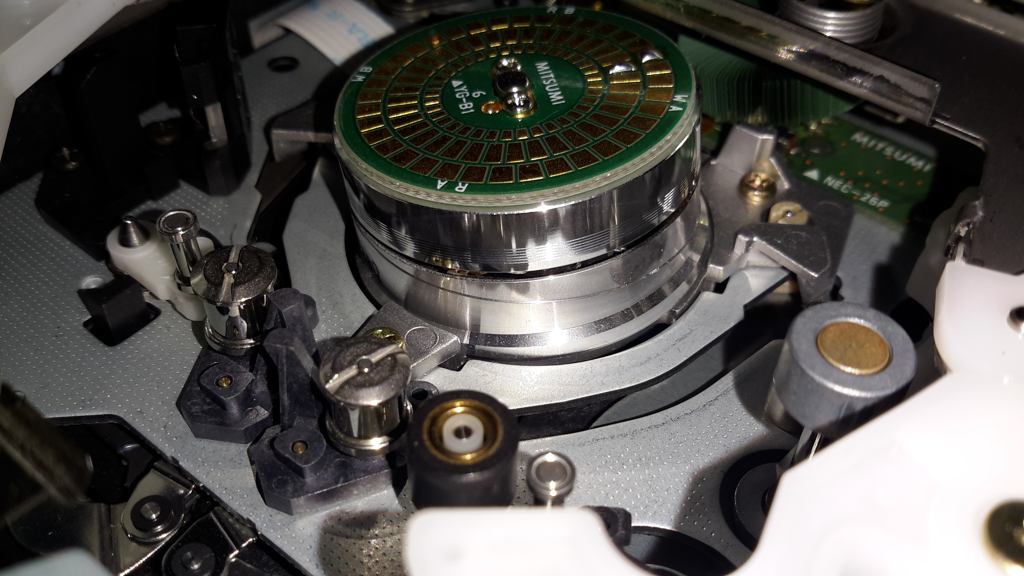
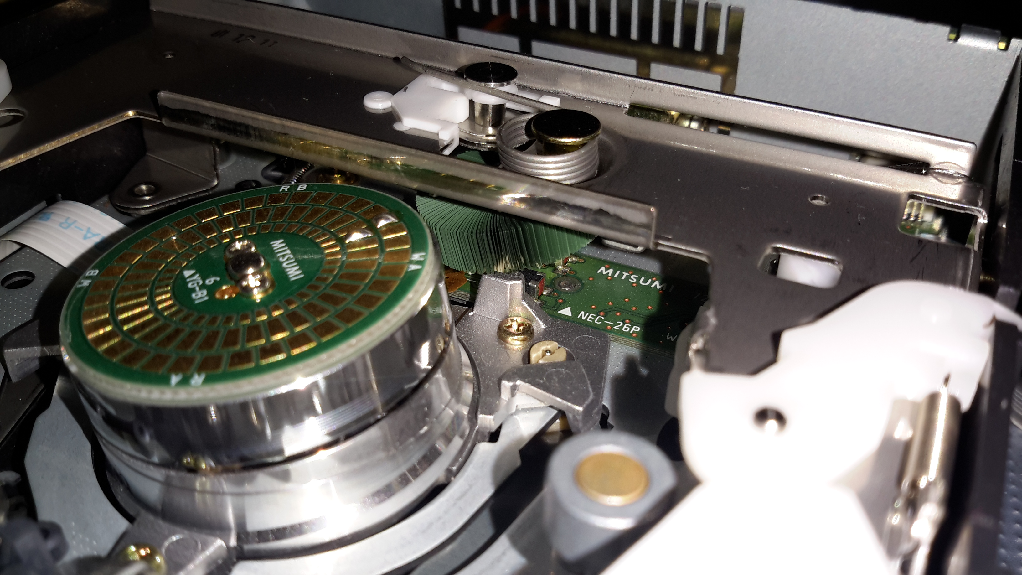
CRT Electron Gun & Flyback Transformer
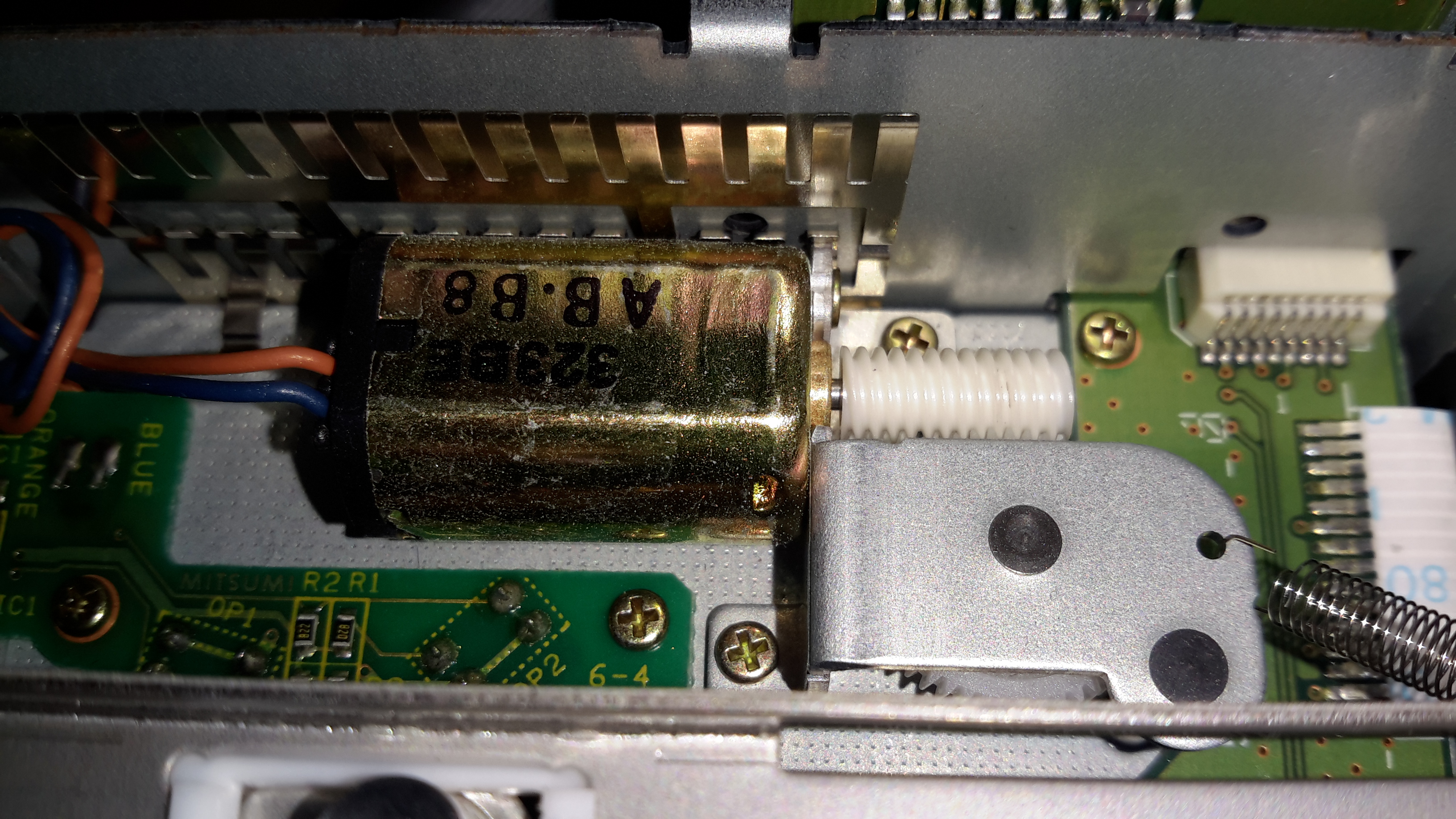
Lifting up the main board reveals more PCBs – the high voltage section for the CRT with the flyback transformer, focus & brightness controls is on the left. The loudspeaker PCB is below this. The CRT electron gun is tucked in behind the flyback transformer, it’s socket being connected to the rest of the circuitry with a flat flex cable.
CRT Rear
Here’s the back of the CRT, the phosphor screen is on the other side of the curved glass back. These tubes must require some additional deflection complexity, as the geometry will change as the beam scans across the screen. There’s a dynamic focus circuit on the schematics, along with extensive keystone adjustments.
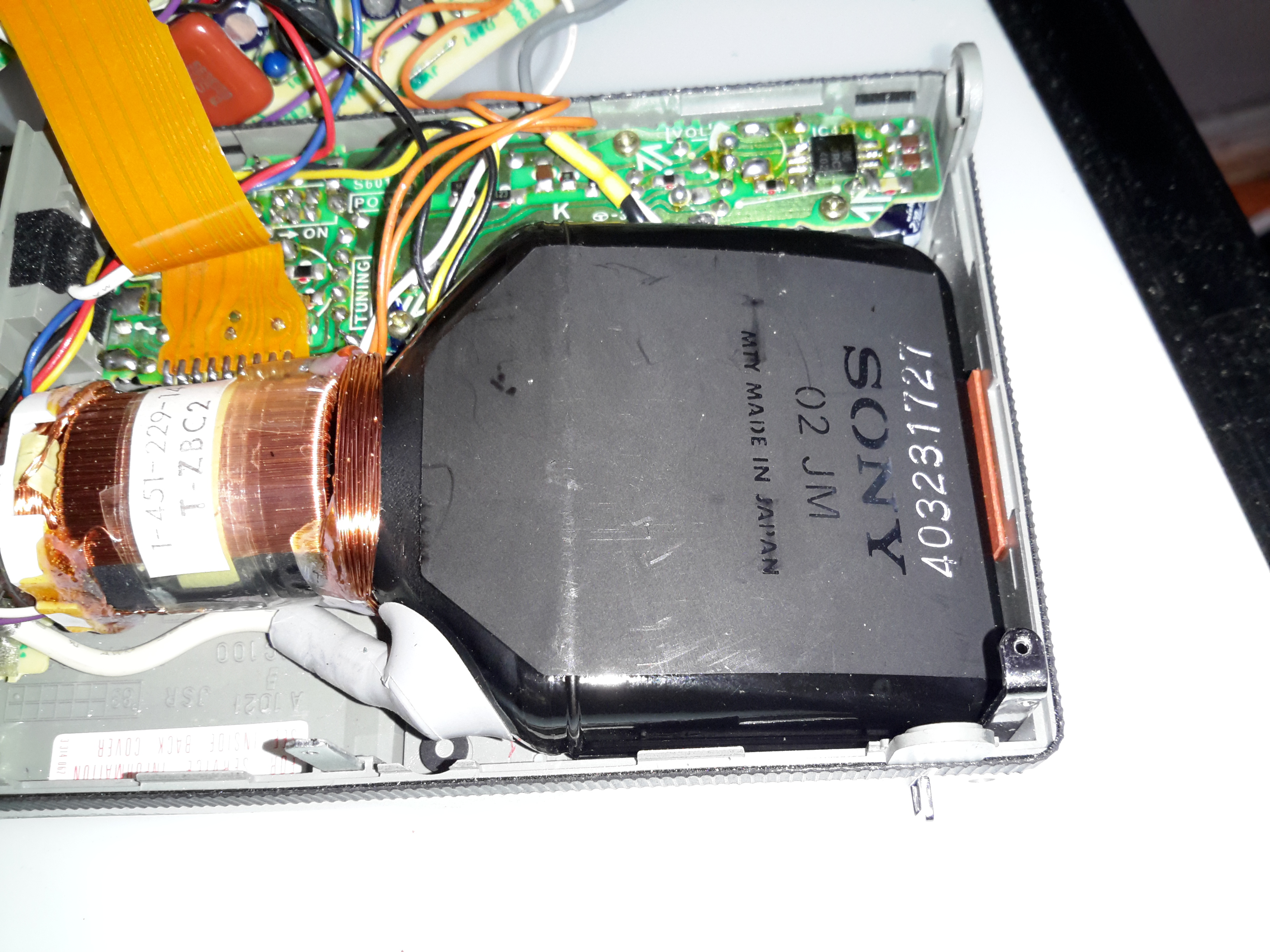
Sony 02-JM Flat CRT
Here’s the tube entirely extracted from the chassis. The EHT connection to the final anode is on the side of the tube bell, the curved phosphor screen is clearly visible. The one thing I can’t find in this CRT is a getter spot, so Sony may have a way of getting a pure enough vacuum that one isn’t required.
I’d expect the vertical deflection waveforms to be vastly different on this kind of CRT, due to the strange screen setup. Not much of a beam movement is required to move the spot from the top to the bottom of the screen.
HV Module
No doubt to keep the isolation gaps large, all the high voltages are kept on a separate small PCB with the flyback transformer. This board generates the voltages for the electron gun filament, focus grid & the bias to set the beam current (brightness) as well.
Bare CRT
Here the deflection yoke has been removed from the CRT, showing the very odd shape better. These tubes are constructed of 3 pieces of glass, the bell with electron gun, back glass with phosphor screen & front viewing window glass. All these components are joined with glass frit.
Electron Gun
The electron gun in the neck looks to be pretty much standard, with all the usual electrodes.
Viewing Window
Here’s a view from the very top of the CRT, the curve in the screen is very obvious here. The electron beam emerges from the bell at the back.
FD-20 Schematic
Here’s the full schematic of the entire TV, I extracted this from a service manual I managed to find online.
More to come on hacking this unit to accept a standard composite video input, from something such as a Raspberry Pi!
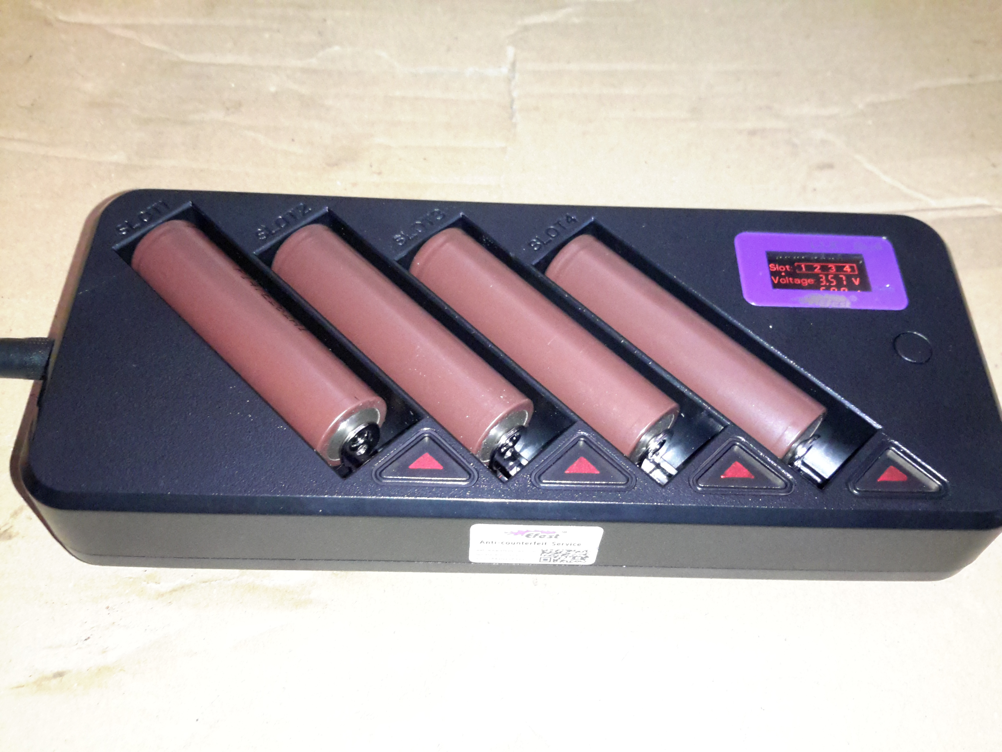
Here’s another battery charger designed for lithium chemistry cells, the BLU4. This charger doesn’t display much on it’s built in LCD, apart from basic cell voltage & charging current limits, as it has a built in Bluetooth module that will link into an Android or iOS app.
Above the charger is operating with 4 brand new cells, at a current of 500mA per cell. If only a pair of cells is being charged, the current can be increased to 1A per cell.
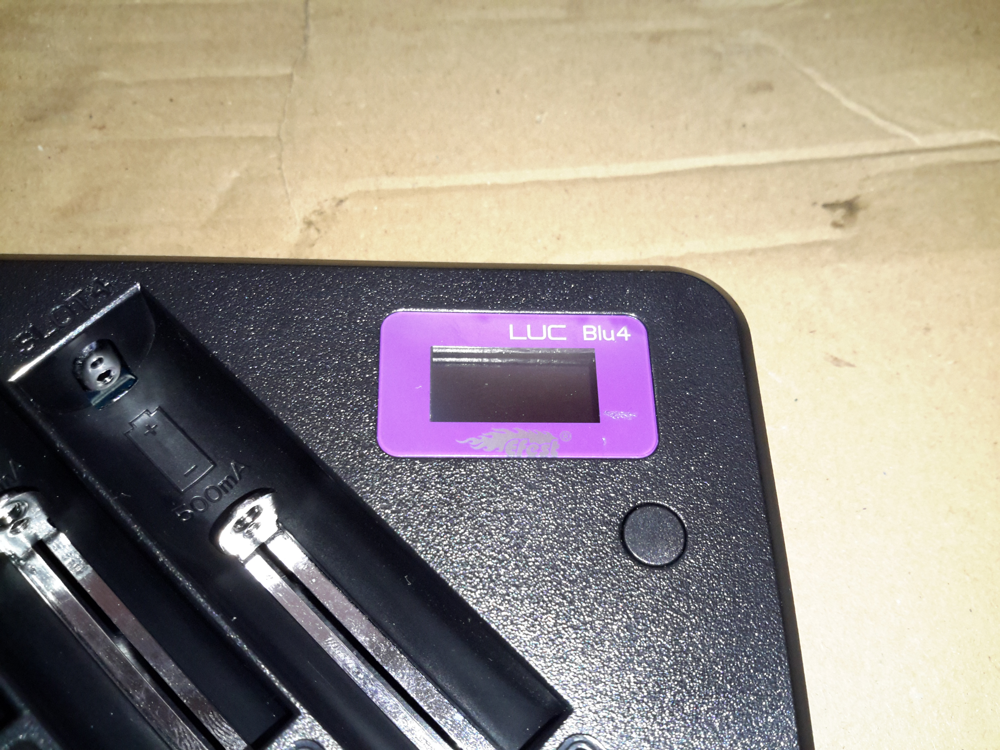
LCD
Not much in the way of user interface on the charger, a tiny LCD & single button for cycling through the display options.
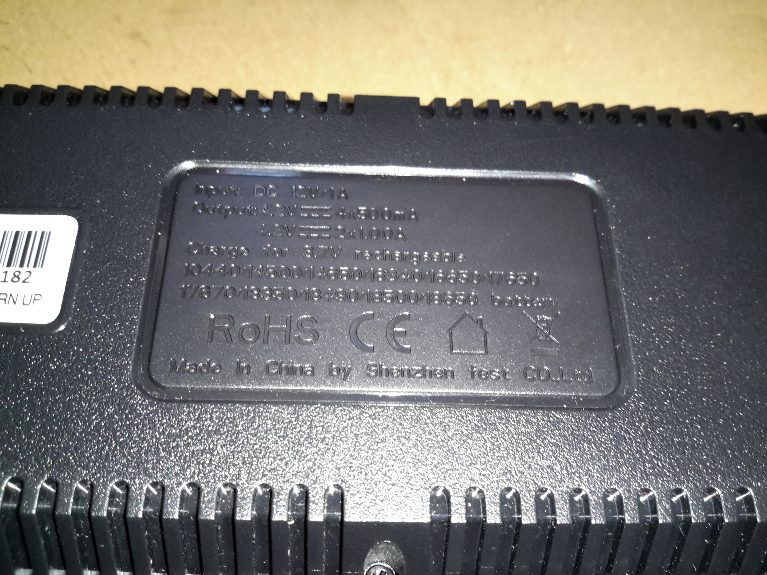
Dataplate
The usual stuff on the data plate, the charger accepts an input of 12v DC at 1A.
Bottom Cover Removed
Removing the 6 screws on the bottom of the casing allows the board to be seen. Not much on the bottom, the 4 cell negative connections can be seen, with their springs for adjusting for cell length.
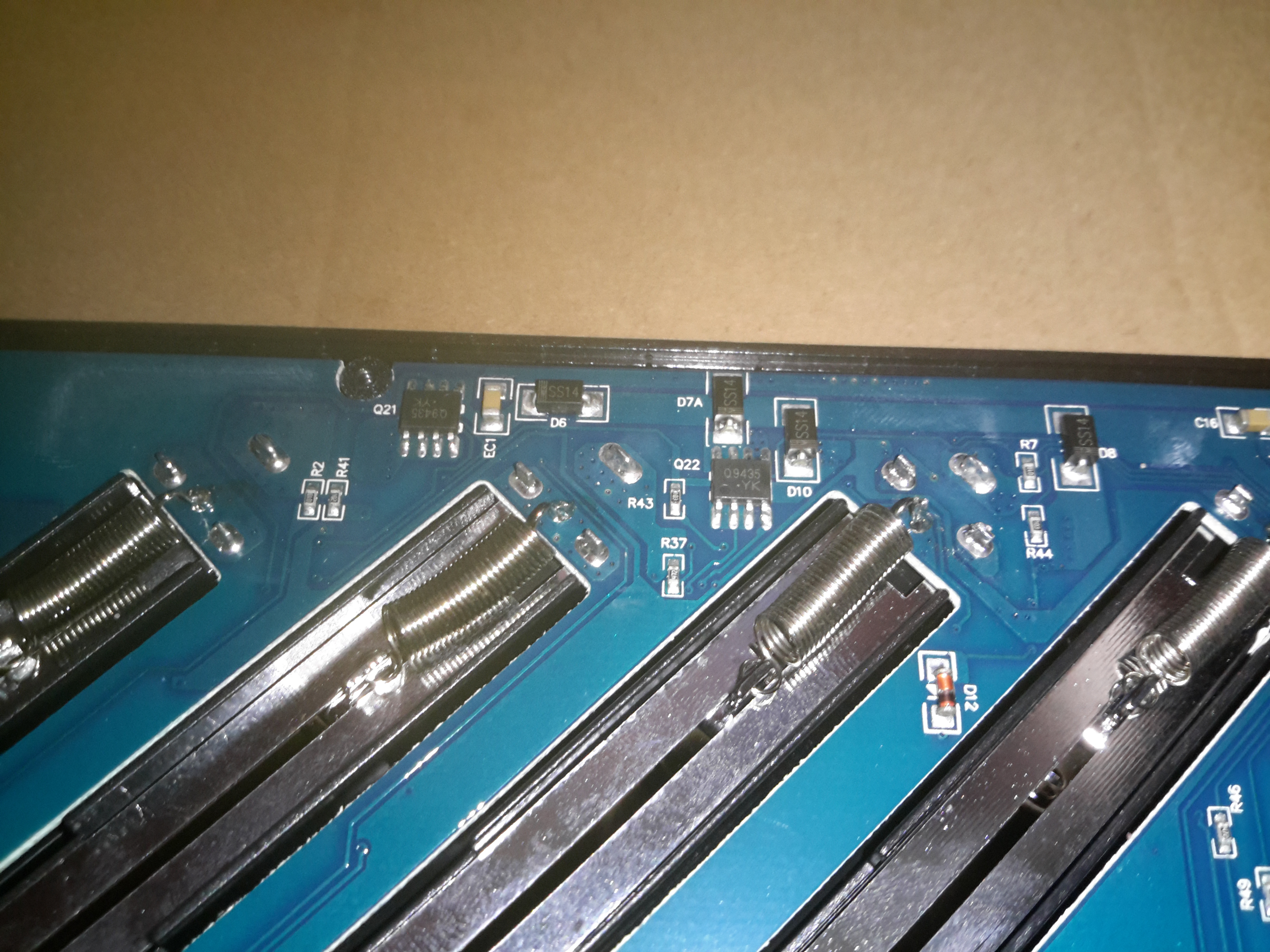
MOSFETs
There’s a couple of P-Channel FETs on the bottom side for the charging circuits, along with some diodes.
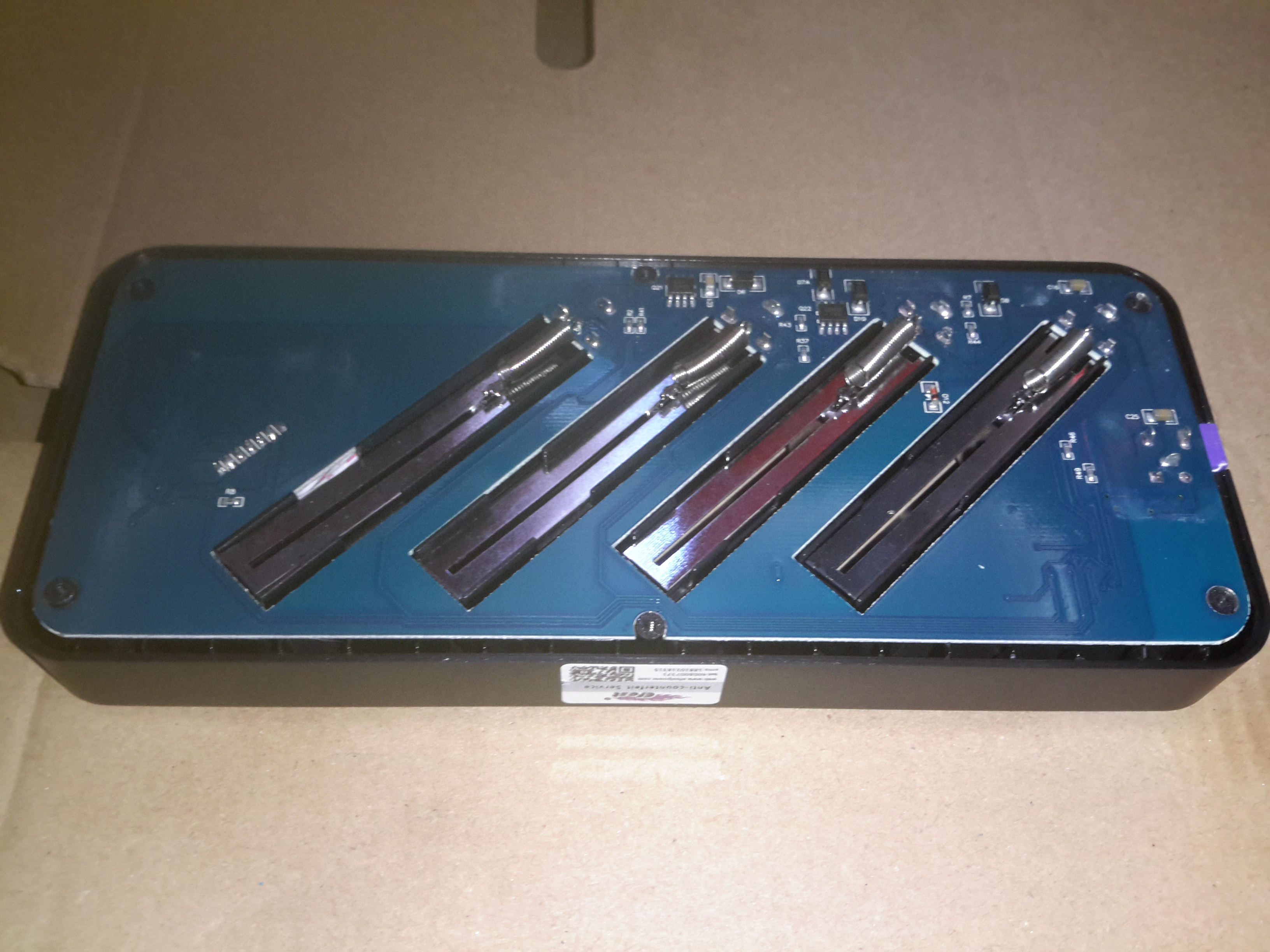
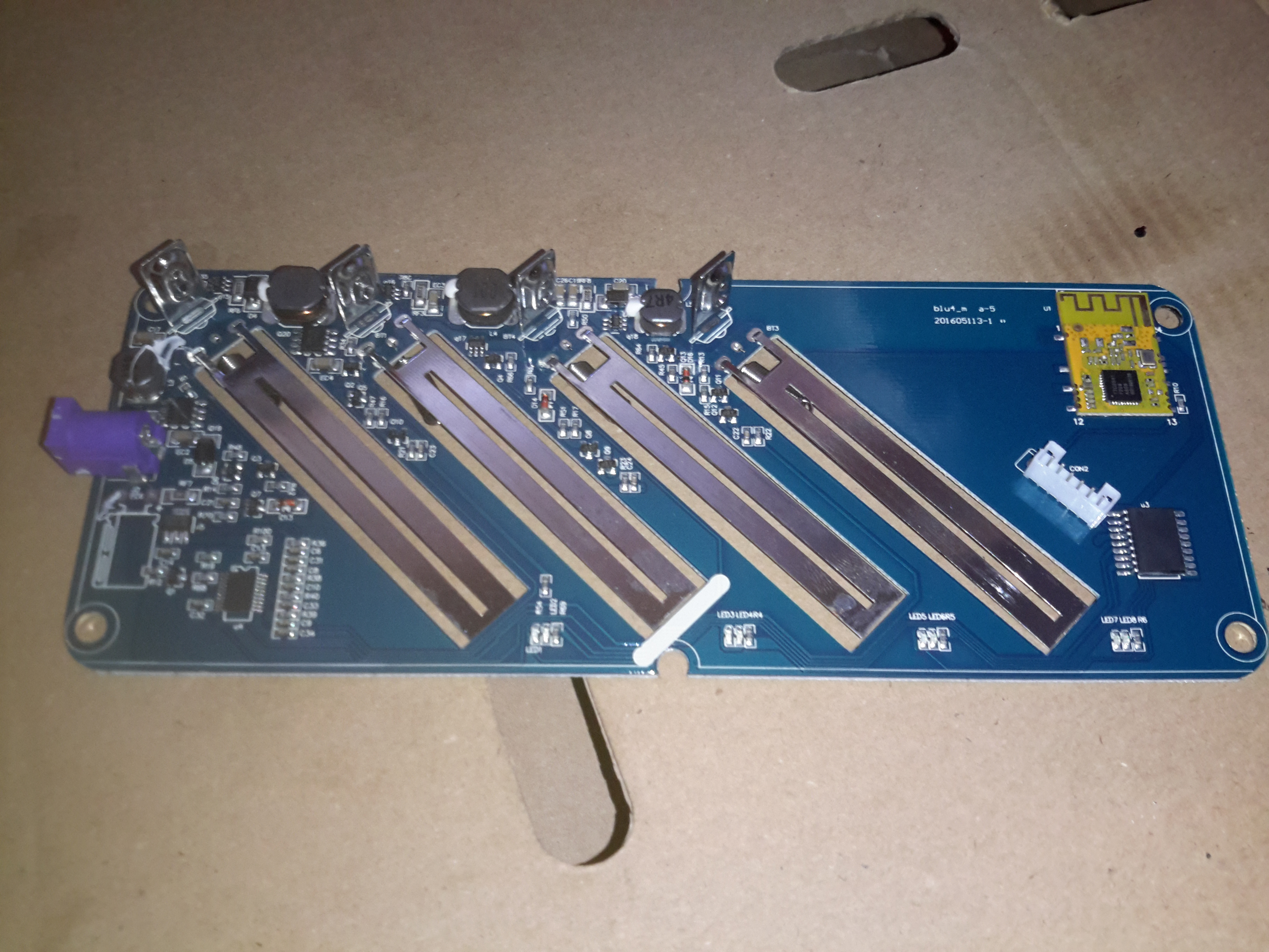
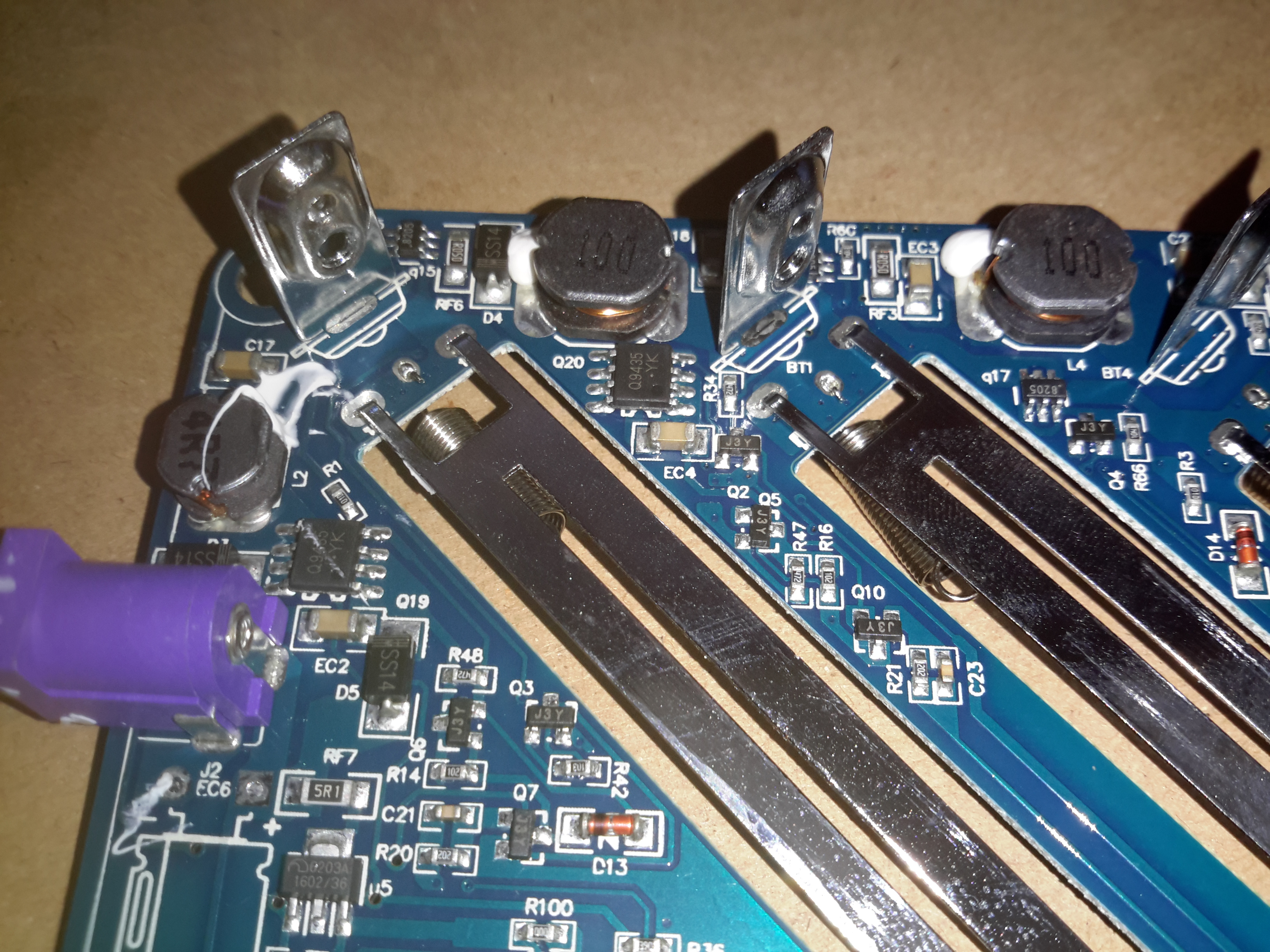
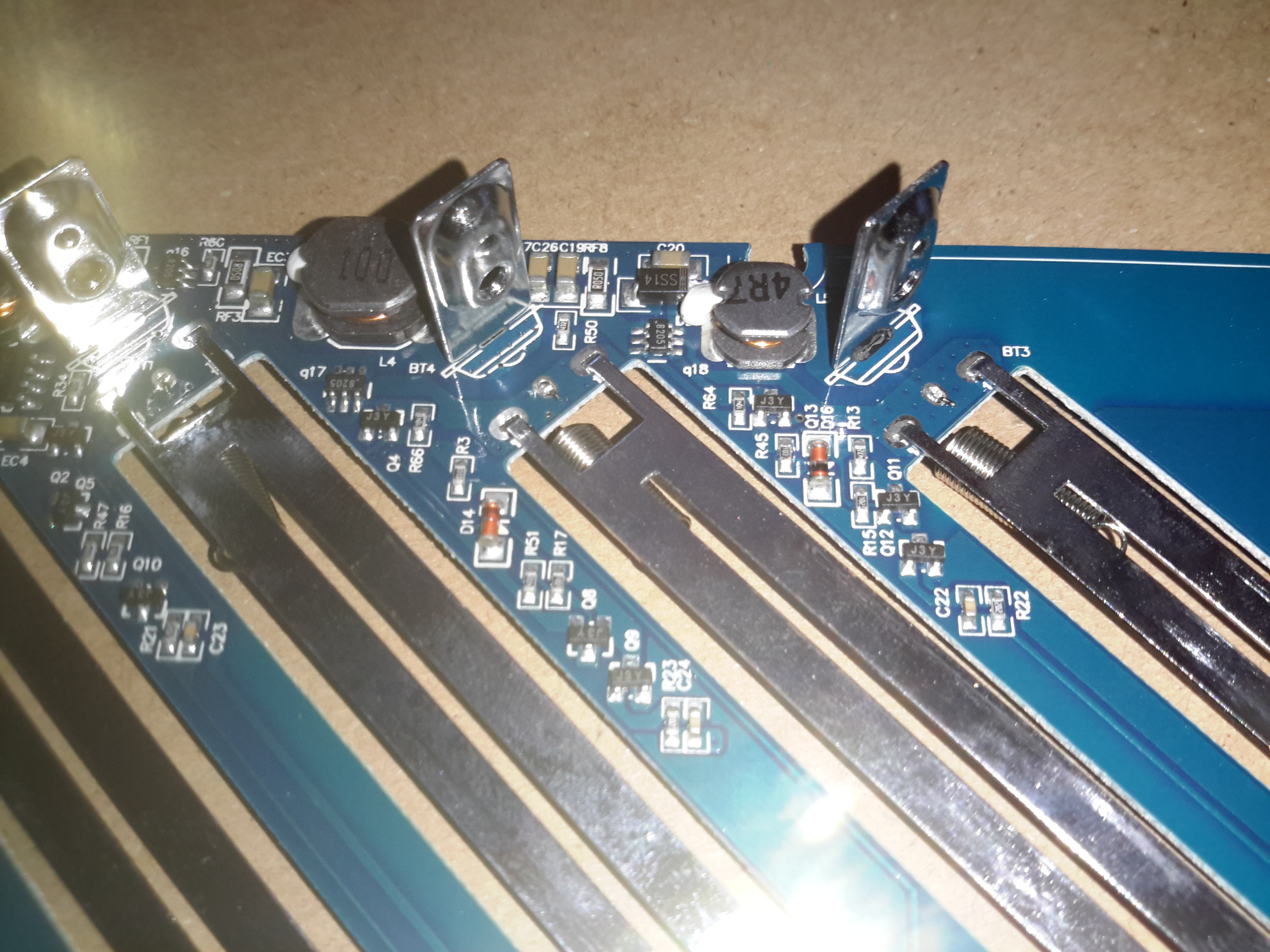
Main PCB
The main PCB is easily removed after the springs are unhooked from the terminals. Most of the power circuitry is located on the top side near the power input. There are 4 DC-DC converters on board for stepping the input 12v down to the 4.2v required to charge a lithium cell.
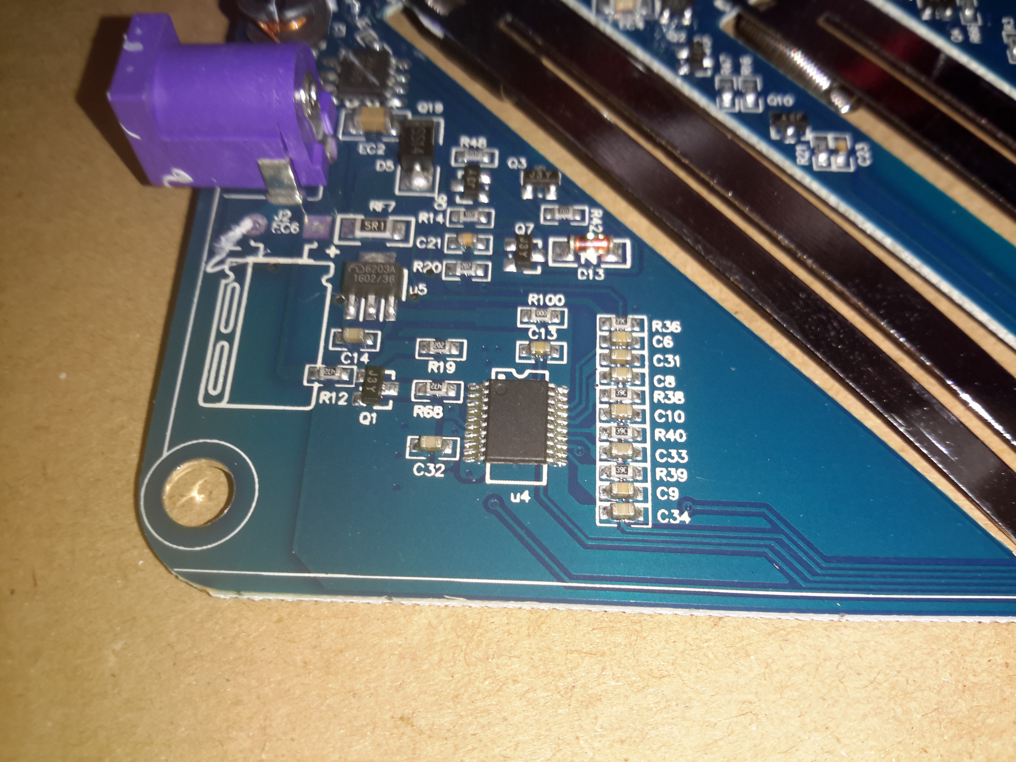
Second Controller
Not entirely sure what this IC is in the bottom corner, as it’s completely unmarked. I’m guessing it’s a microcontroller though.
DC Input Side
The top left of the board is crammed with the DC-DC converters, all the FETs are in SO8 packages.
DC-DC Converters
One pair of DC-DC inductors is larger than the other pair, for reasons I’m unsure of.
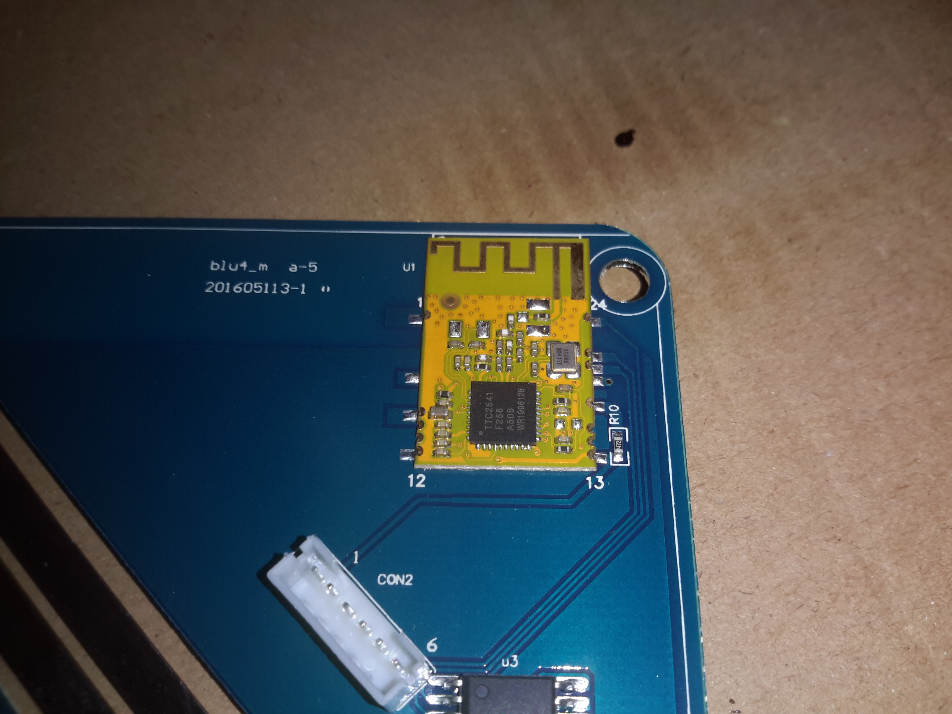
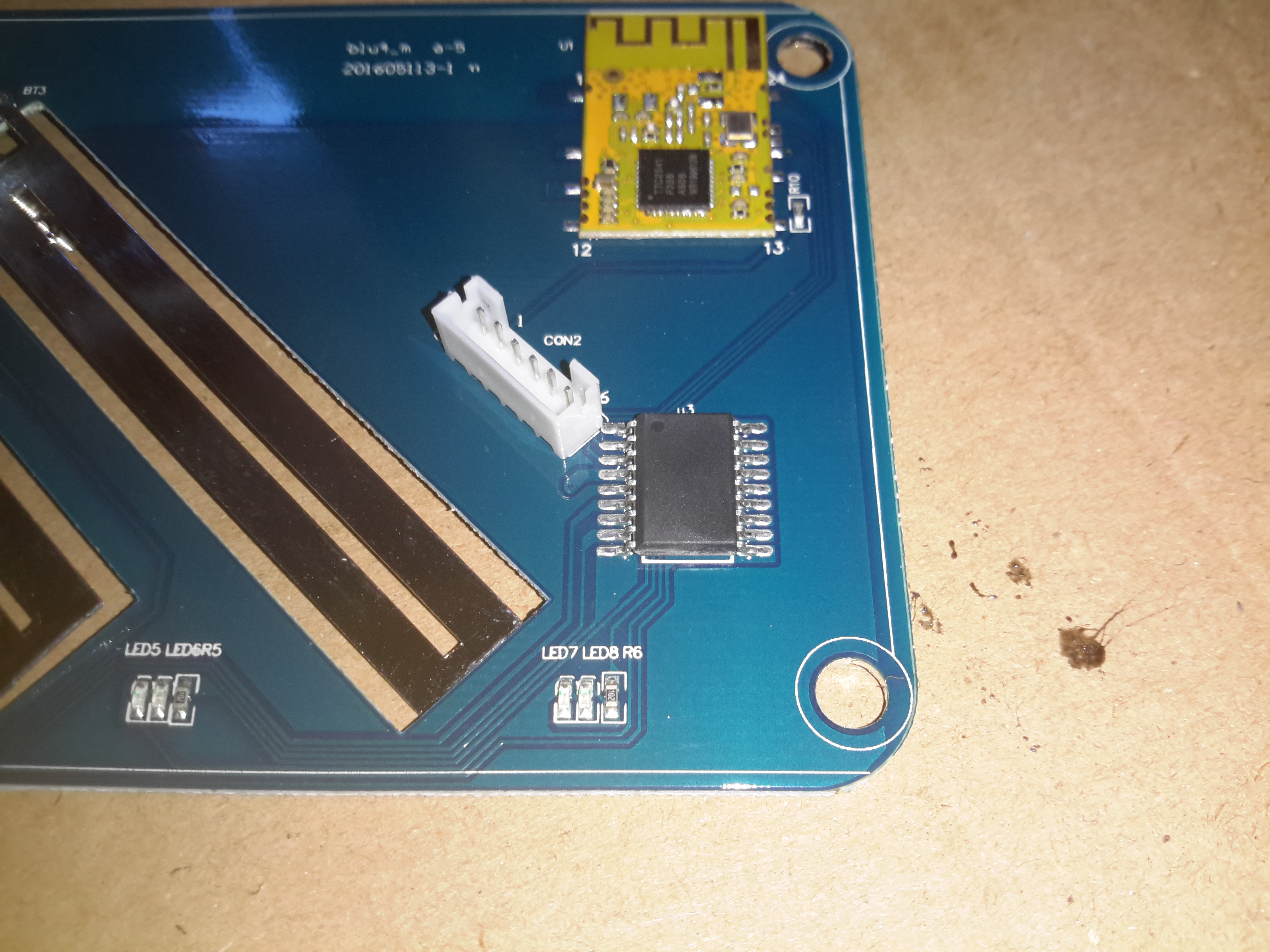
Bluetooth Module
Bluetooth connectivity is provided by this module, which is based around a TTC2541 BLE IC.
Microcontroller
Below the Bluetooth module is yet another completely unmarked IC, the direct link to the BLE interface probably means it’s another microcontroller. The Socket to the left of the IC is the connector for the front panel LCD & button.
LCD PCB
There’s not much to the LCD itself, so I won’t remove this board. The LCD controller is a COB type device, from the number of connections it most likely communicates with the micro via serial.
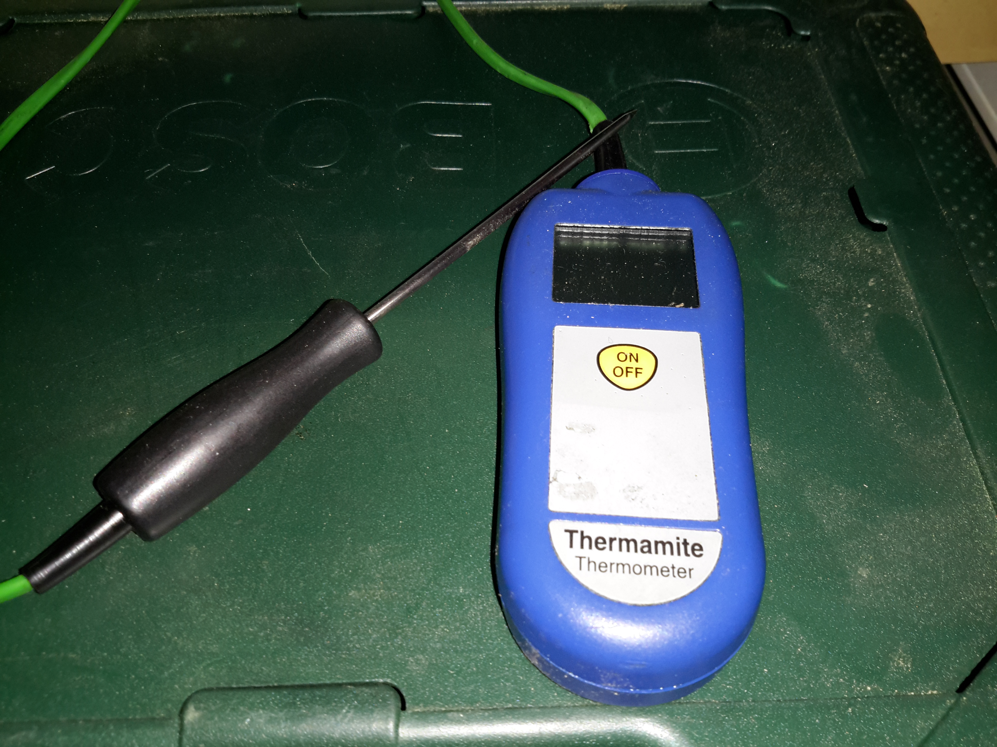
Here’s another bit of commercial gear, a catering thermometer. These are used to check the internal temperature of foods such as meat, to ensure they’re cooked through.
This was given to me with some damage, the battery cover is missing & the plastic casing itself is cracked.
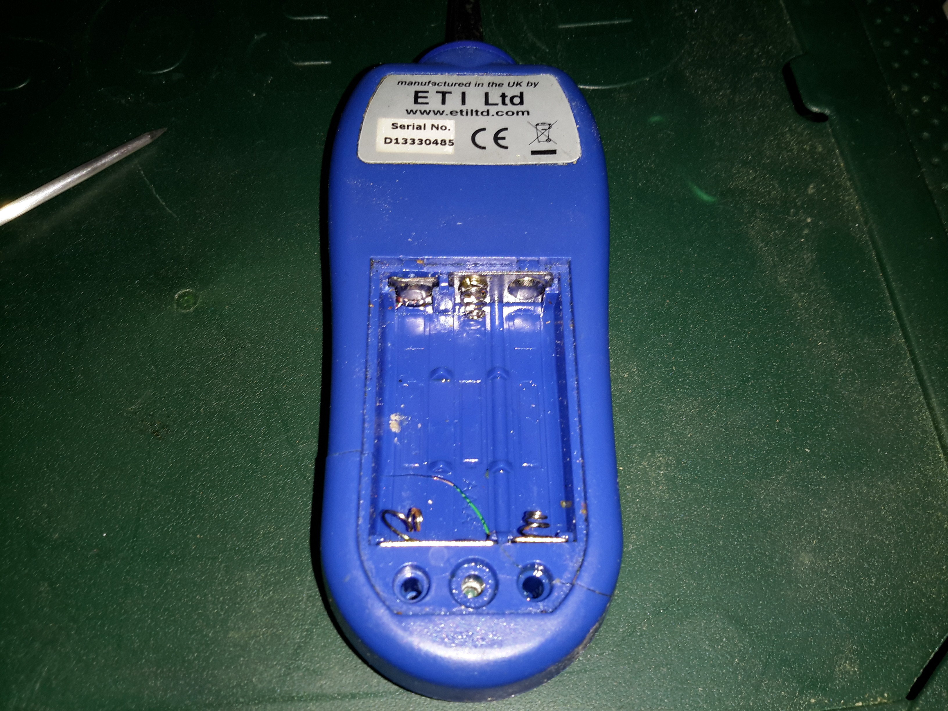
Battery Compartment
Power is provided by 3 AAA cells, for 4.5v
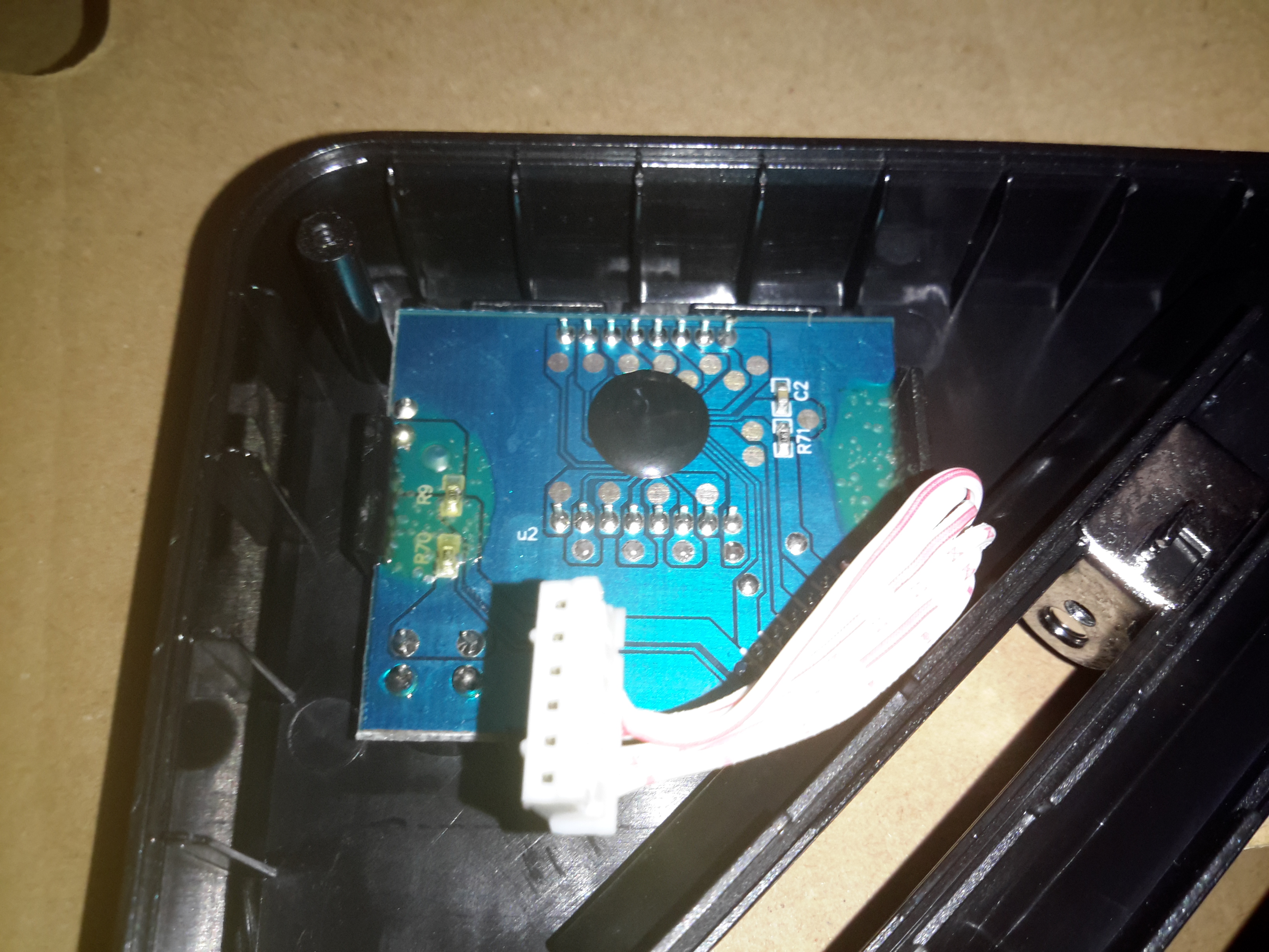
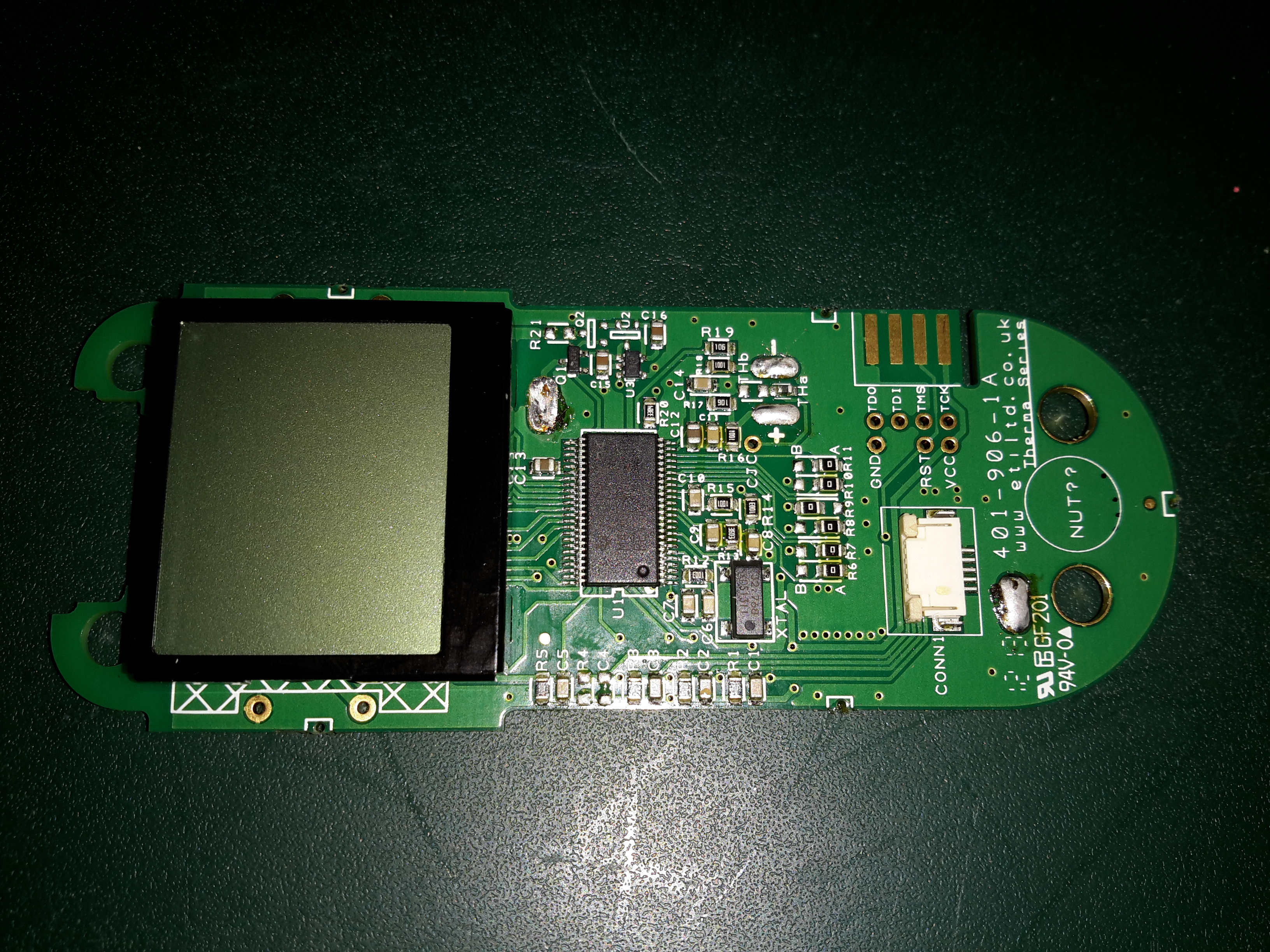
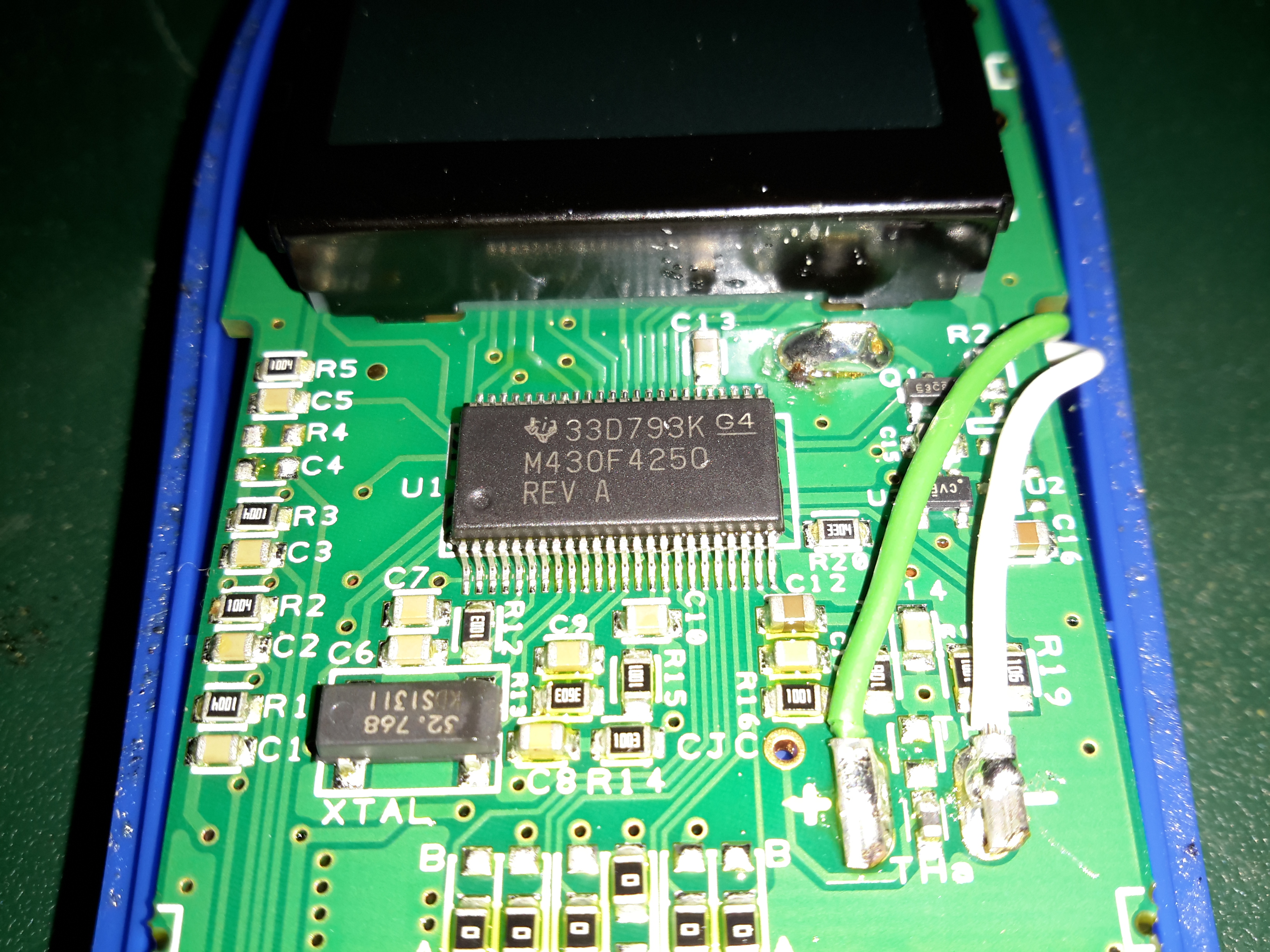
Main PCB
There’s not much to these units, the large LCD at the top is driven by the IC in the centre. A programming header is also present on the board near the edge.
Microcontroller
The core logic is taken care of with a Texas Instruments M430F4250 MSP430 Mixed-Signal Microcontroller. This MCU has onboard 16-bit Sigma-Delta A/D converter, 16-bit D/A converter & LCD driver. Clock is provided by a 32.768kHz crystal.
The probe itself is just a simple thermistor bonded into a stainless steel rod.
SG-HM2 is a modular He-Ne laser power supply based on IC-HI1 with some minor enhancements. The first version is for laser tubes up to approximately 1 mW (2 mW with trivial modifications) but it should be straightforward to go to 5 mW or even higher power tubes by replacing the SG-HM2 HV Module (HVM2-1) with one with a higher voltage and current rating, along with a higher power MOSFET and minor component value changes to the Control Module (suggestions below). I have added an adjustment for tube current, a current limiting resistor and Zener to protect against output short circuits, an enable input (ground to turn on), a bleeder resistor to virtually eliminate the shock hazard after the power supply is turned off, and power and status LEDs.
Get the schematic for SG-HM2 (1 mW version) in PDF format: [download id=”5610″]
Modifying SG-HM2 for Higher Power He-Ne Laser Tubes
The following are guidelines for modifying SG-HM2 to drive various power He-Ne lasers. The PCB layout below with two versions of the HV Module should accommodate He-Ne laser tubes up to 10 mW. All assume input of around 12 V though a higher power system can generally run lower power lasers at reduced input voltage. If operation at rated power on another input voltage is desired, the number of turns on the inverter transformer can be adjusted accordingly. As noted above, the 1 mW HV Module (HVM2-1) should run tubes up to about 2 mW, though increasing the µF values of some of the HV capacitors may be desirable to reduce ripple at the higher tube current. Minor changes may also be needed in the components on the SG-HM2 Control Module including using a higher power MOSFET for Q1 and reducing the values of R7 and/or R8 for the higher tube current. Or, just populate the Control Module with Q1 being an IRF644, R7 being 150 ohms, and R8 being 750 ohms for compatibility with all the HV modules. For that matter, the HVM2-5 PCB HV Module should be usable with lower power lasers.
   Laser Power       1 mW         2 mW         5 mW         10 mW
-----------------------------------------------------------------------
   Voltage           1200 V       1500 V       2300 V       3500 V
   Current           2-4mA        3-5mA        5-7mA        5-7mA

 SG-HM2 HV Module:

   PCB Version       HVM2-1       HVM2-1       HVM2-5       HVM2-5

   T101
    Core (DxH)       18x11 mm     18x11 mm     26x16 mm     26/16 mm
    Primary          9T,#28       9T,#28       9T,#26       9T,#26
    Secondary        450T,#40     450T,#40     600T,#40     900T,#40
     Res. (Est)      60 ohms      60 ohms      (90 ohms)    (120 ohms)

   D101-106          2kV          2kV          3kV          5kV

   C101-104          1nF,3kV      2nF,3kV      2nF,6kV      2nF,6kV
   C105              47pF,3kV     47pF,3kV     100pF,6kV    100pF,6kV
   C106              3nF,10kV     5nF,10kV     6nF,15kV     6nF,15kV

   R102              10K,1/2W     10K,1/2W     10K,1W       10K,1W
   R103              200M,10kV    200M,10kV    200M,15kV    200M,15kV
   R106-107 (total)  10M          10M          15M          20M

 SG-HM2 Control Module:

   Q1              IRF630       IRF630       IRF640       IRF644
   R7              300          250          150          150
   R8              500          250          100          100
SG-HM2 Inverter Transformer
The inverter transformer for HVM2-1 is wound on a ferrite pot core with a small air-gap (about 0.005″). It is 18 mm in diameter by 11 mm high. While specified to use a 9 turn primary and 450 turn secondary, these values can be adjusted somewhat to handle various input and output requirements. Don’t go much lower on the primary as this may result in core saturation. The 9/450 transformer should be fine for 1 to 2 mW He-Ne laser tubes running on 8 to 15v DC input. With 9/300, it will operate on about 12 to 20v DC. Increasing the number of secondary turns (e.g., 9/600) may result in operation on a slightly lower input voltage, but probably not by much. The 9/450 transformer may even run He-Ne laser tubes larger than 2 mW but I haven’t yet tested this since I haven’t built a prototype of HVM2-5 as yet.
It doesn’t matter very much whether the primary (P) is wound first or the secondary (S) is wound first though the former appears to work slightly better, running the tube at about 8v DC input instead of 9v DC input for the same 9/450 transformer. P over S is slightly easier to wind since the primary doesn’t get in the way and increase the lumpiness of the secondary layers. However, with S over P, insulation is somewhat less critical since the HV lead is out away from anything else. With the P over S, additional insulation is needed between them. Also, since the primary coil is larger diameter, it will have more resistance and there will be greater inter-winding capacitance (though probably not significant). The secondary should be constructed as multiple layers of about 50 or 60 turns each, with insulating tape between layers. Each should be wound in as close to a single layer as possible with alternating layers staggered to prevent arc-over. This doesn’t have to be perfect but try to go gradually from one side to the other to keep wires at high relative potential away from each other. Make sure the HV output leads (particularly the one away from the dot) are well insulated as they exit the transformer. And, as noted, if the primary is over the secondary, there must be high voltage insulation between them. The peak output voltage when the MOSFET turns off (the flyback pulse) may be more than 5 times higher than what would be expected from the DC input voltage and the turns-ratio alone – several kV and this *will* try to find a path to ground! There are more detailed transformer construction instructions in the next section.
Note that this transformer is slightly larger physically than the one from IC-HI1. This is for two reasons: (1) It is easier to wind with more space and a larger wire size for the secondary, and (2) continuous operation should be possible with 2 mW laser tubes, which might have been marginal with the original transformer used in IC-HI1. A by-product of the larger core is that its 9 turn primary should be roughly equivalent to the 12 turn primary of the smaller core in terms of inductance and core saturation limitations.
Interestingly, a similar transformer found in a different commercial power supply, had no insulating tape anywhere. It would appear that with very precise machine-wound HV secondary, done first, the voltage is distributed so uniformly that this is unnecessary.
I’ve now built and tested several transformers in IC-HI1, removing the original transformer and installing socket pins so either the original or an adapter board can be plugged in. This setup is then equivalent to SG-HM2 with the HVM2-1 HV Module. The minimum input voltage values that follow are when driving a 0.5 mW He-Ne laser tube:
           Turns        Pot Core   Vin (VDC)
   ID   P/S    Order    (DxH mm)   Min  Max           Comments
 ------------------------------------------------------------------------------
   1* 12/600  S over P    14x8     7.5  15   Original IC-HI1 transformer
   2  12/350  S over P    18x11    14   22   First prototype, described above
   3   9/350  S over P    18x11    11   18   #2 with 3 P T added out-of-phase
   4   9/425  P over S    18x11     9   16
   5   9/450  P over S    18x11     9   16
   6   9/450  S over P    18x11     8   15
   7  12/500  P over S    26x16     8   15
*The number of turns on the original (#1) is not really known exactly and may be lower or higher by up to 25 percent based on the measured secondary resistance (45 ohms) and estimated wire size (somewhere between #38 and #40. (Even with the larger wire, the amount of bobbin area taken up by the wire is less than 50 percent so it should fit even with many layers of insulating tape. The transformer is Epoxy impregnated and likely to be impossible to disassemble into any form that can be analyzed!)
All of these transformers will drive He-Ne laser tubes of up to at least 2.5mW using the equivalent of the HVM2-1 HV Module which is part of IC-HI1. Even with the 2.5mW tube, the minimum operating voltage was only about 0.5v higher than for the 0.5mW tube. There is a good chance they would drive even larger He-Ne laser tubes (though possibly at a slightly higher input voltage) but I don’t dare try using the existing HV circuitry as it might not survive for long. I suspect that transformers #4, #5, and #6 would run on an input voltage of less than 8v DC but the salvaged cores I am using have a larger air-gap than might be optimal and I don’t have anything to reduce it without heavy losses. They attempt to start the tube at around 6v DC but are unable to maintain it and flicker rapidly. (#2 and #3, which use the same style core, would also benefit somewhat.) Operation using #1 and #5 is virtually identical, with the original running at perhaps 0.5v DC less input. I expect they would be even more identical if the air-gap on #5 were smaller, and #6 with its smaller air-gap does indeed run at the lower input voltage. I haven’t actually confirmed that anything blows up above the maximum voltages listed above, which were arbitrarily chosen. But I am guessing that bad things might happen at some point. 🙂
I have also constructed a transformer which will need to be used with HVM2-5: 12/1200, P over S, on a 30×19 pot core. I will also construct a 9/900. S over P, on a 30×19 pot core (or on a 26×16 if I can find one). Testing of these will have to await an HVM2-5 prototype.
SG-HM2 Transformer Construction
Here are details on construction of the inverter transformer for SG-HM2. With all parts and tools on hand, it takes about an hour start to finish. Only a small portion of this time is in the actual winding (at least if a coil winding machine is used). Most of the time is spent in adding the insulation tape and terminating the leads. After constructing a few of these, it does go quicker. 🙂
Step-by-step instructions are provided for the HVM2-1 transformer. The changes needed for HVM2-5 are summarized at the end of this section. Some sort of coil winding machine is almost essential as #40 wire is extremely thin and easy to break. (Anything larger than #40 will not fit on the bobbin.) It doesn’t have to be fancy. Mine is probably 50 years old of the type that is (used to be?) advertised in the back of electronics magazines. However, a couple of spindles – one that is fixed or free to rotate for the wire supply and the other which can be turned for the coil being wound – are really all that are needed. Don’t use any sort of powered approach though (unless you have a *real* professional coil winder!) as it is all too easy to break the wire if there is no tactile feedback to detect snags.
Parts required for T101 of HVM2-1:
18×11 mm (1811) ferrite pot core with a small air-gap (no more than 0.005″) or no air-gap, and a single section bobbin. These are available from several manufacturers but surplus or salvaged cores may be easier to obtain. Radio Shack used to have a “ferrite kit” which included a variety of sizes of cores (only 1 each though so you’d have to buy two kits and there were no bobbins!). I doubt the kit still exists though.
Approximately 1.5 feet of #28 magnet wire for the primary (9 turns wound first) and approximately 60 feet of #40 magnet wire for the secondary (450 turns wound on top of the primary). I found both these size wire in various solenoids and relays I’ve discombobulated. 🙂 Wire sizes aren’t critical but these are known to fit and the #40 can be handled with a reasonable chance of not breaking.
Sleeving to protect the primary wires where they leave transformer. I used approximately 2″ of insulation (each lead) from the individual wires in some 25 pair phone cable.
Wirewrap wire or other thin insulated wire to terminate the secondary wires where they leave the transformer.
Insulating tape. 1 mil Mylar or similar is desirable. However, I’ve found that thin clear (non-reinforced) packing tape does an adequate job, though it probably doesn’t have as much dielectric strength as real insulating tape so additional layers are required. It will also likely not stand up to overheating too well. Electrical tape is way too thick and would prevent enough turns from fitting.
A piece of Perf. board with holes on 0.1″ centers, 0.8″x0.8″. There should be 7 rows of holes each way so that one hole lines up in the center.
A Nylon 4-40 screw and nut to fasten the transformer to the board.
Four (4) machined-type IC socket pins or something similar to use as terminals.
Wind the primary:
Slip a piece of sleeving over the start of the primary wire and position the sleeving so it extends about 1/2 turn inside the bobbin on the left side.
Wrap exactly 9 turns of this wire clockwise around the bobbin, left to right. The wires should enter and exit on the same angular position (slot) of the bobbin on opposite sides.
Slip another piece of sleeving over the wire end exiting the bobbin so that it too is about 1/2 turn inside the bobbin.
Wrap 1.5 to 2 turns of tape tightly over the primary winding to secure and insulate it.
Wind the secondary:
Strip 1/8″ or so from the end of a 2″ piece of wire-wrap wire and solder the start of the wire for the secondary winding to it. Make sure the insulation on the fine magnet wire has been removed – usually just heating it while soldering will do this. Leave an inch or so of the magnet wire extending from the connection so that continuity can be confirmed with a multimeter, then snip it off. Install this in the opposite slot of the bobbin also on the left side with about 1/4″ of insulation inside the bobbin against the side and separated from the primary. Leave a little slack in the fine secondary wire so that slight motion won’t break it. Add a small piece of tape to protect and insulate this connection.
Using your coil winding machine (you do have one, correct?), build up the secondary in layers of about 50 to 75 turns in a counter-clockwise direction (bobbin being rotated clockwise). A single layer of wire won’t fit in the 1/8″ or so available (in the 18×11 mm core bobbin) so there will have to be some overlap. But, do this several times across the layer so that any given wire won’t be next to one with a much different voltage. In other words, wind a few turns and back up so that there will in essence be multiple sub-windings of 5 or 10 turns, repeated several times across the layer. Keep the wire at least 1/32″ away from either edge of the bobbin.
After each full layer or wire, add just over 1 layer of insulating tape making sure it covers the entire width of the bobbin. There should be just enough overlap to assure there is at least 1 layer of insulation but not much more as excessive tape will end up taking up too much space.The entire 450 turn winding will then require 6 to 9 full layers. Add another layer of insulating tape over the last winding layer leaving the wire end exposed.
Terminate the end of the secondary winding with another piece of thin wire by soldering as above. Confirm continuity with a multimeter. For the 450 turn secondary, the resistance should be about 60 ohms. Add a piece of thicker sleeving over this at the HV end if space is available. Else, use some bits of tape to insulate the wirewrap wire lead from the core and exposed inner layers that it may come near as it exits out the side of the bobbin. Add another layer of tape to secure the lead in place.
Add several more layers of insulating tape to complete the bobbin assembly.
Prepare the mounting board:
Widen the center hole to 7/64″ to accommodate a 4-40 nylon screw.
Widen the holes at the 4 corners of the board to accept the 4 IC socket pins (if used) as a press-fit or glue them in place with 5 minute Epoxy or SuperGlue.
Final assembly:
Install the ferrite pot core halves to the bobbin taking care not to crunch any of the wires. Orient it so that the primary and secondary leads are conveniently located with respect to the 4 pins, e.g., primary start: bottom left; primary end: top left, secondary start: bottom right; and primary end: top right.
Use the nylon 4-40 screw and nut to *gently* secure the transformer to the mounting board. The head of the 4-40 screw should be underneath the board. Don’t over-tighten or it may crack the core, especially if it has an air-gap in the middle.
Carefully remove the insulation from the ends of the wires. The secondary wires will still be fragile even with the wirewrap wire terminations. For the magnet wire, the easiest way to remove the insulation is to burn it off with a match or hot soldering iron and then clean with fine sandpaper.
Push the wires into their respective socket pins. (The wirewrap wires are too thin to be secure but they will make adequate contact for testing.)
Use a multimeter to confirm continuity of the primary (close to 0 ohms) and secondary (about 50 to 75 ohms).
Testing:
Install the transformer in you HV Module. Attach a He-Ne laser tube and ballast resistor.
Power up on an variable DC power supply and check for reliable starting and stable operation. Adjust the core gap if needed. A smaller gap may result in more operating power available at a given input voltage. A larger gap will result in attempts to start on a lower input voltage. Somewhere around 0.005″ is probably a good compromise.
After testing the transformer (and adjusting the core gap if needed), use some adhesive to secure the pot core sections and to protect the transformer leads. Solder the leads into the socket pins.
The final result is shown on an adapter below:
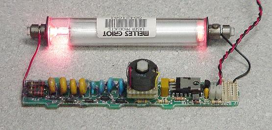
Photo of SG-HM2 HVM2-1 Transformer being Tested in IC-HI1
The instructions for winding the HVM2-5 transformer are similar except for the dimensions, wire sizes and lengths, and number of turns for the primary and secondary:
Differences in parts list for T501 of HVM2-5 compared to T101 of HVM2-1:
26×16 mm (2616) ferrite pot core with a small air-gap (no more than 0.005″) or no air-gap, and a single section bobbin.
Approximately 2.0 feet of #26 magnet wire for the primary (12 turns wound first) and approximately 75 to 120 feet of #40 magnet wire for the secondary (600 or 900 turns wound on top of the primary).
A piece of Perf. board with holes on 0.1″ centers, 1.0″x1.0″. There should be 9 rows of holes each way so that one hole lines up in the center.
A Nylon 10-32 screw and nut to fasten the transformer to the board.
Since the peak voltage on the HVM2-5 secondary may be 2 to 3 times higher than for HVM2-1, extra insulation and clearances will be required on the secondary.
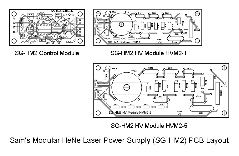
SG-HM2 Printed Circuit Board Layout
A printed circuit board layout is also available. The Control Module is 2″x1.2″. The HV Modules are 3.6″x1.2″ and 4.5″x1.8″ for the 1 mW (HVM2-1) and 5 mW (HVM2-5), respectively. The Control and HV Modules are connected by a 2 pin cable for transformer drive and a 3 pin cable for current sensing from the laser tube. The two boards can easily be merged if desired.
The layout of the 3 PCBs may be viewed as a GIF file (draft quality) as below:
Sam’s Modular He-Ne Laser Power Supply 2 PCB Layout
.
A complete PCB artwork package for SG-HM2 (all PCBs on one sheet) may be downloaded in standard (full resolution 1:1) Gerber PCB format (zipped) as [download id=”5612″]
The Gerber files include the component side copper, soldermask, and silkscreen; solder side copper and soldermask, and drill control artwork. The original printed circuit board CAD files and netlist (in Tango PCB format) are provided so that the circuit layout can be modified or imported to another system if desired. The text file ‘sghm2.doc’ (in sghm2grb.zip) describes the file contents in more detail.
Note: The netlist does NOT include wiring for the HVM2-5 HV Module. Also, part numbers on the HVM2-5 PCB actually begin with a “5” instead of a “1” since Tango PCB will not allow duplicate part numbers on the same layout.
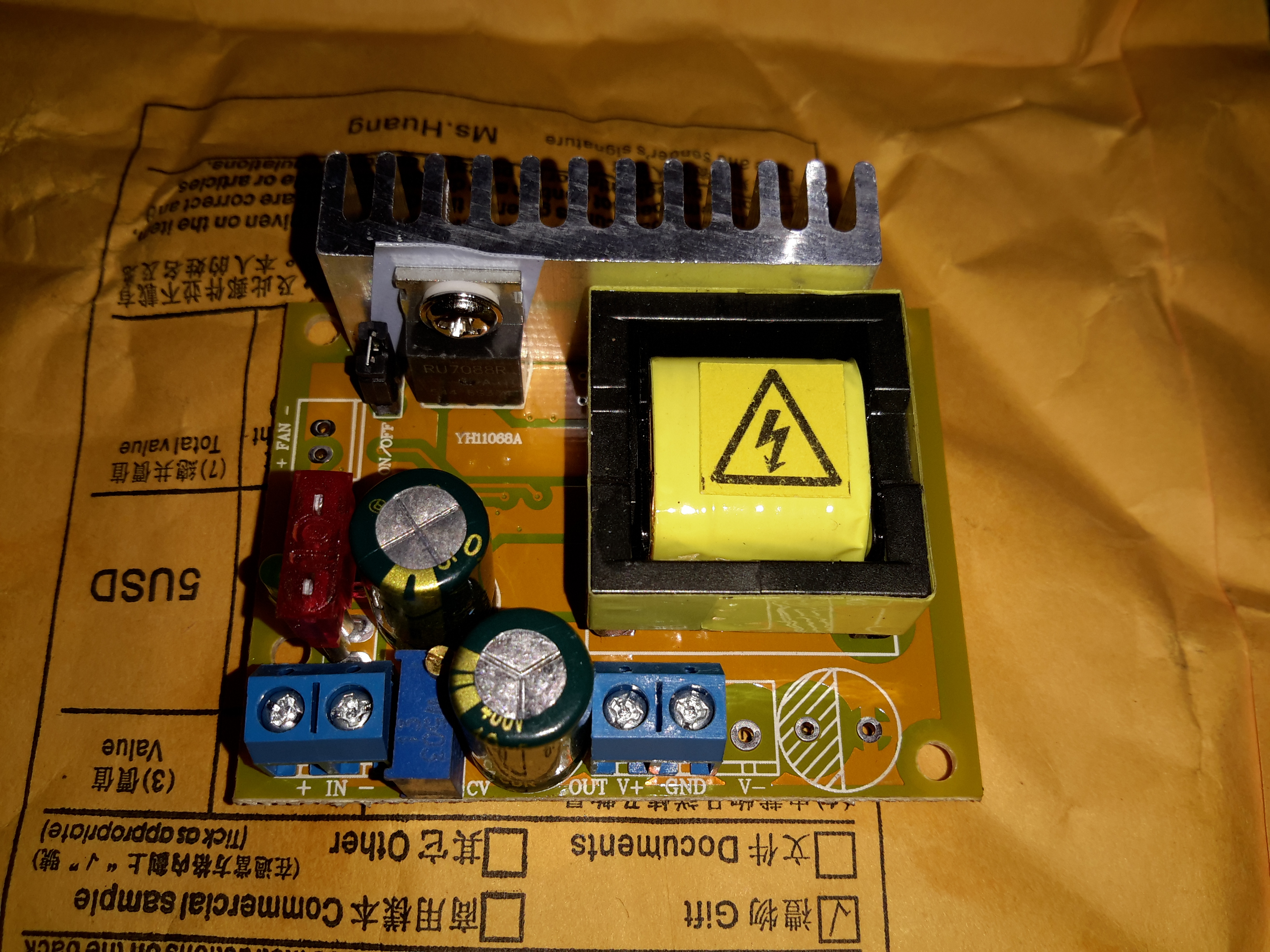
Going through eBay recently looking for parts for a couple of CRT-based projects, I came across these DC-DC converters.
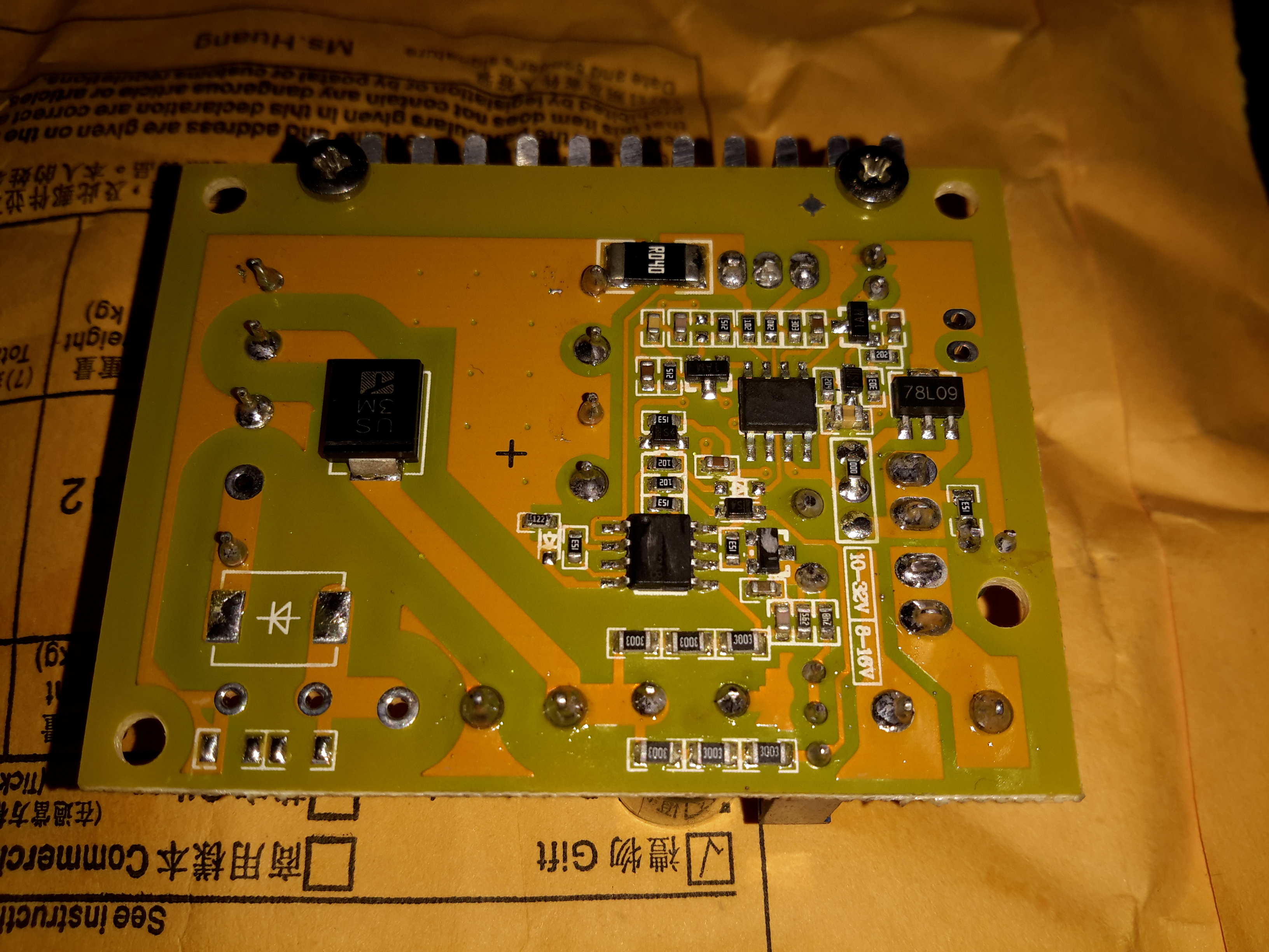
Apparently rated from 45-390v DC output at 200mA, these should be ideal for driving some of the electrodes (focus, screen, grid) in a CRT.
Above is the top of the board, input voltage header on the left, output voltage adjust in the centre & output voltage header on the right.
This module has a mini-automotive fuse, at 10A for input protection.
On the heatsink is mounted the main switching MOSFET, a RU7088R from Ruichips. This FET is fairly heavily rated at 70v 80A, with 6.5mΩ on-resistance.
PCB Bottom
The bottom of the board has the control components, with a pair of ICs. Unfortunately the numbers have been scrubbed off, so no identification here. The output from the transformer is rectified with a single large SMD diode on the left side of the board.
There’s also plenty of isolation gap between the HV output trace & the low voltage logic side of the circuit, the two being bridged only by a resistive divider for output voltage measurement.
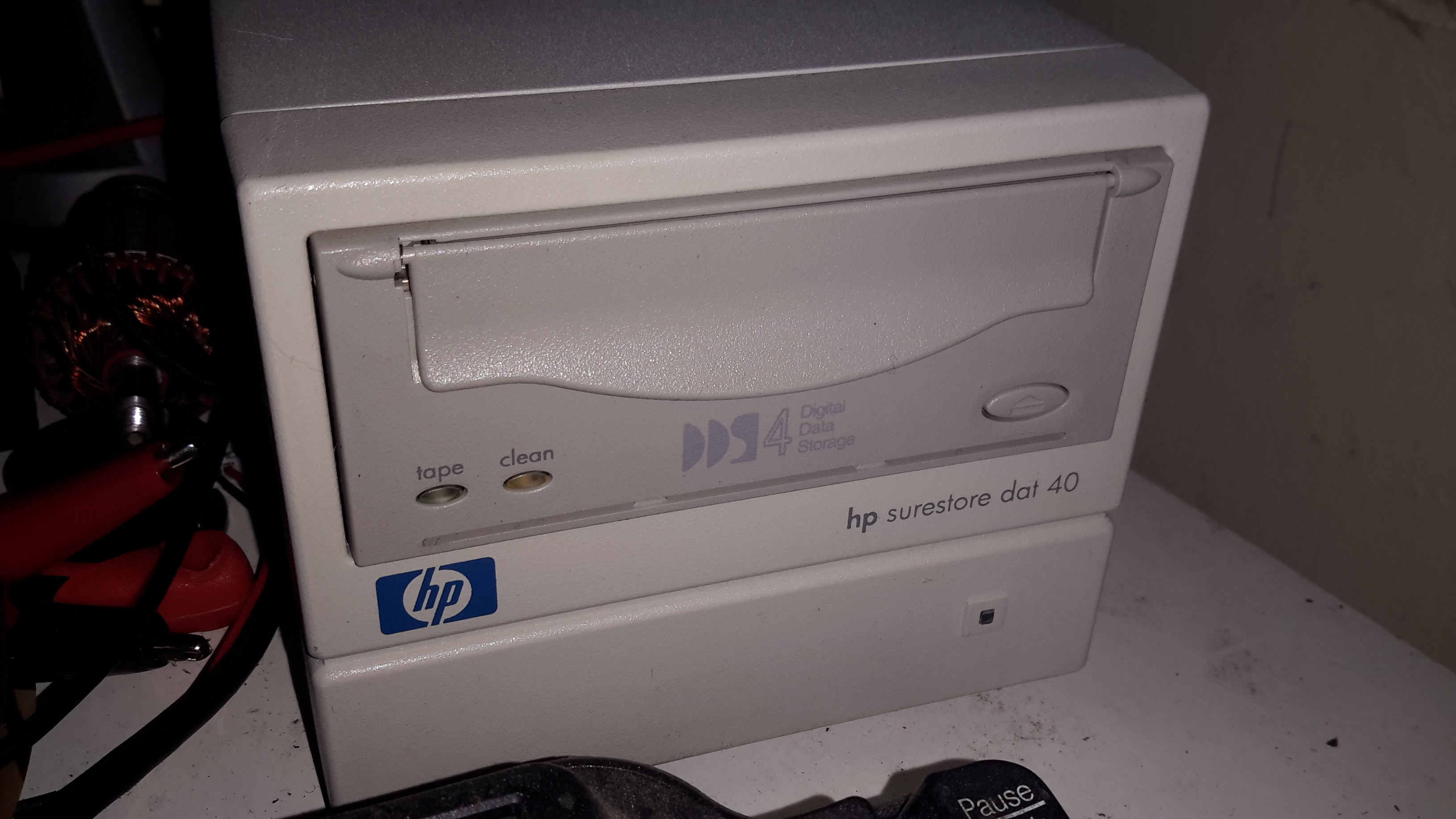
Magnetic tape is the medium of choice for my offline backups & archives, as it’s got an amazing level of durability when in storage. (LTO Has a 30 year archival rating).
For the smaller stuff, like backing up the web server this very site runs on, another format seemed to suit better. Above is a HP DDS4 tape drive, which will store up to 40GB on a cassette compressed.
I picked this format since I already had some tapes, so it made sense.
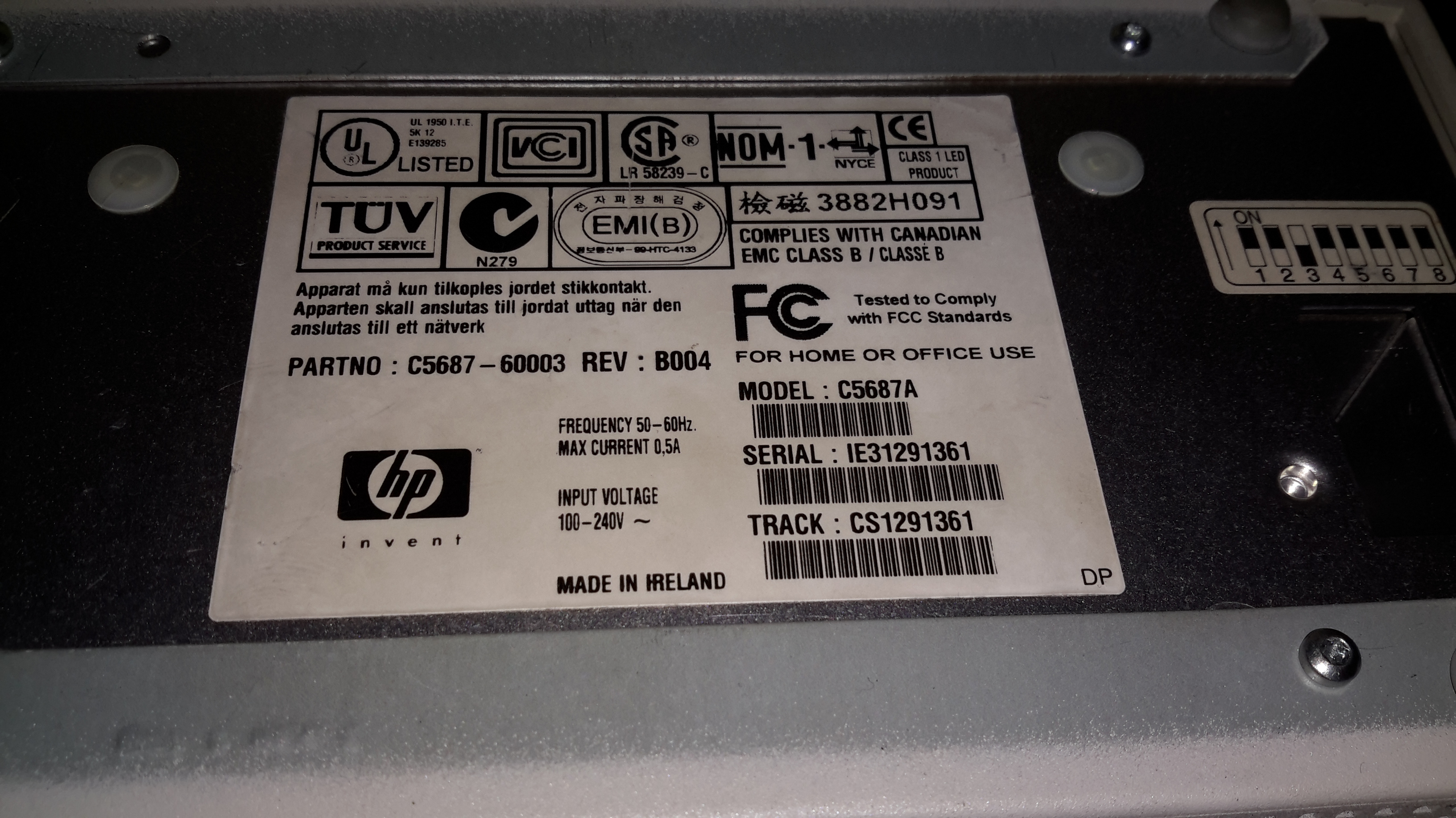
Data Plate
Here’s the info for those who want to know. It’s an older generation drive, mainly since the current generation of tape backup drives are hideously expensive, while the older ones are cheap & plentiful. Unfortunately the older generation of drives are all parallel SCSI, which can be a expensive & awkward to set up. Luckily I already have other parallel SCSI devices, so the support infrastructure for this drive was already in place.
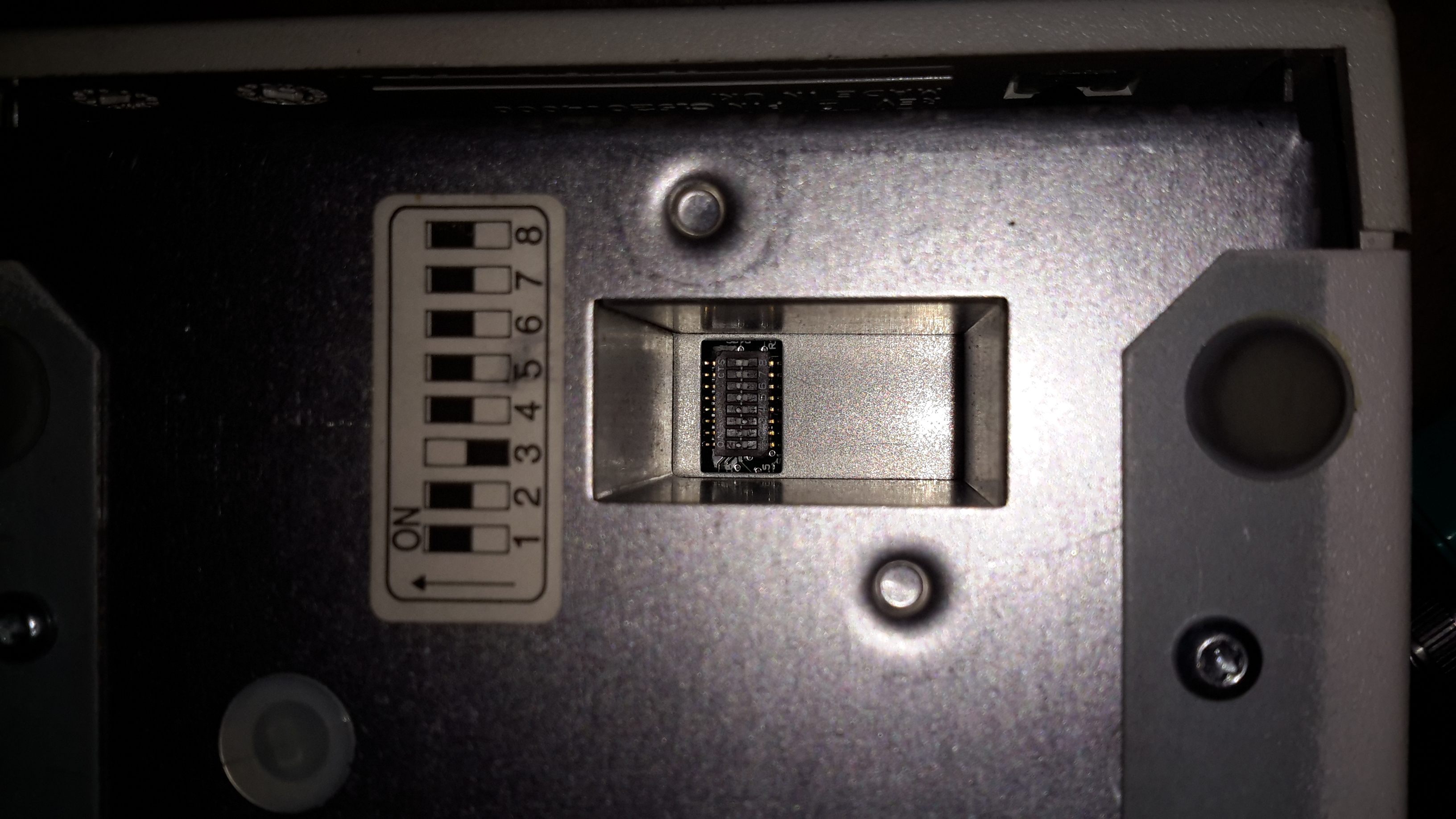
Option Switches
On the bottom of the drive is a bank of DIP switches, according to the manual these are for setting the drive for various flavours of UNIX operating systems. However it doesn’t go into what they actually change.
Controller PCB
The bottom of the drive has the control PCB. The large IC on the left is the SCSI interface, I’ve seen this exact same chip on other SCSI tape drives. Centre is a SoC, like so many of these, not much information available.
Drive Frame
Removing the board doesn’t reveal much else, just the bottom of the frame with the tape spool motors on the right, capstan motor bottom centre. The bottom of the head drum motor is just peeping through the plastic top centre.
Head Drum
Here’s the head drum itself. These drives use a helical-scan flying head system, like old VHS tape decks. The top of the capstan motor is on the bottom right.
Cleaning Brush
Hidden just under the tape transport frame is the head cleaning brush. I’m not sure exactly what this is made of, but it seems to be plastic.
Loading Motor
A single small DC motor with a worm drive handles all tape loading tasks. The PCB to the bottom left of the motor holds several break-beam sensors that tell the drive what position the transport is in.
Tape Transport Mech
Here’s the overall tape transport. The PCB on top of the head drum is a novel idea: it’s sole purpose in life is to act as a substrate for solder blobs, used for balancing. As this drum spins at 11,400RPM when a DDS4 tape is in the drive, any slight imbalance would cause destructive vibration.
Tape Transport
Here’s the drive active & writing a tape. (A daily backup of this web server actually). The green head cleaning brush can be better seen here. The drive constantly reads back what it writes to the tape, and if it detects an error, applies this brush momentarily to the drum to clean any shed oxide off the heads. The tape itself is threaded over all the guides, around the drum, then through the capstan & pinch roller.
I recently came across these on eBay, so I thought I’d grab one to see how they function, with all the metrics they display, there’s potential here for them to be very useful indeed.
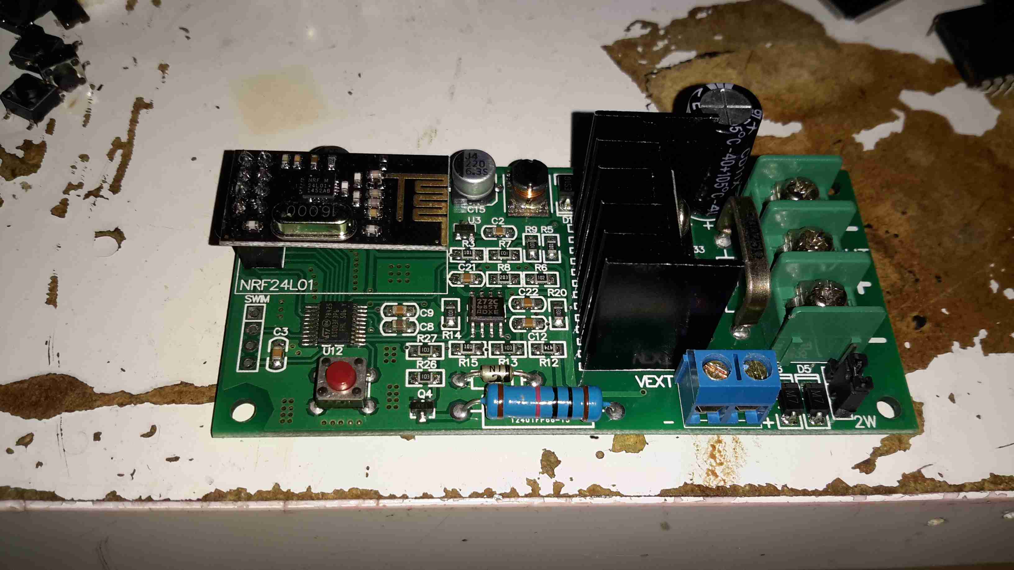
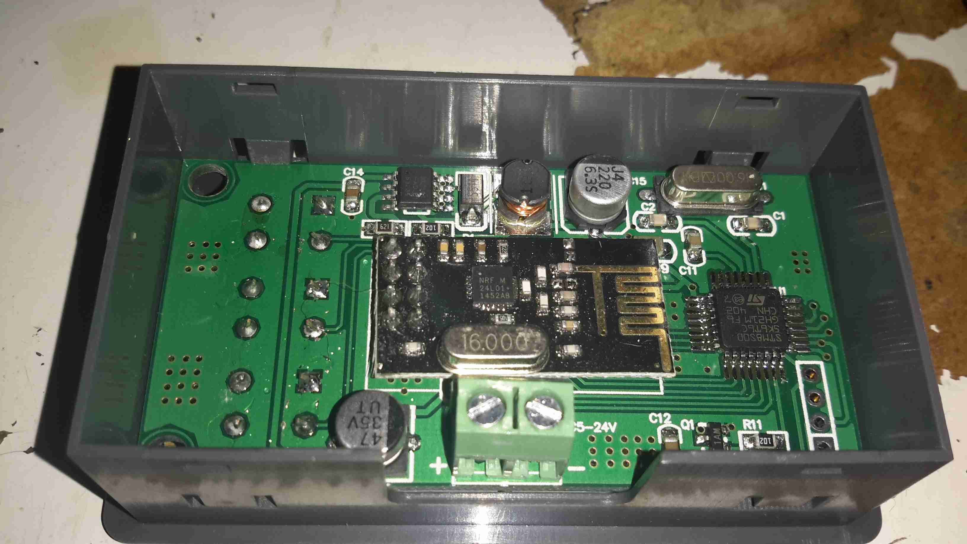
One of the best parts is that no wiring is required between the sensor board & the LCD head unit – everything is transmitted over a 2.4GHz data link using NRF24L01 modules.
Above is the display unit, with it’s colour LCD display. Many features are available on this, & they appear to be designed for battery powered systems.
Monitor PCB
Another PCB handles the current & voltage sensing, so this one can be mounted as close to the high current wiring as possible.
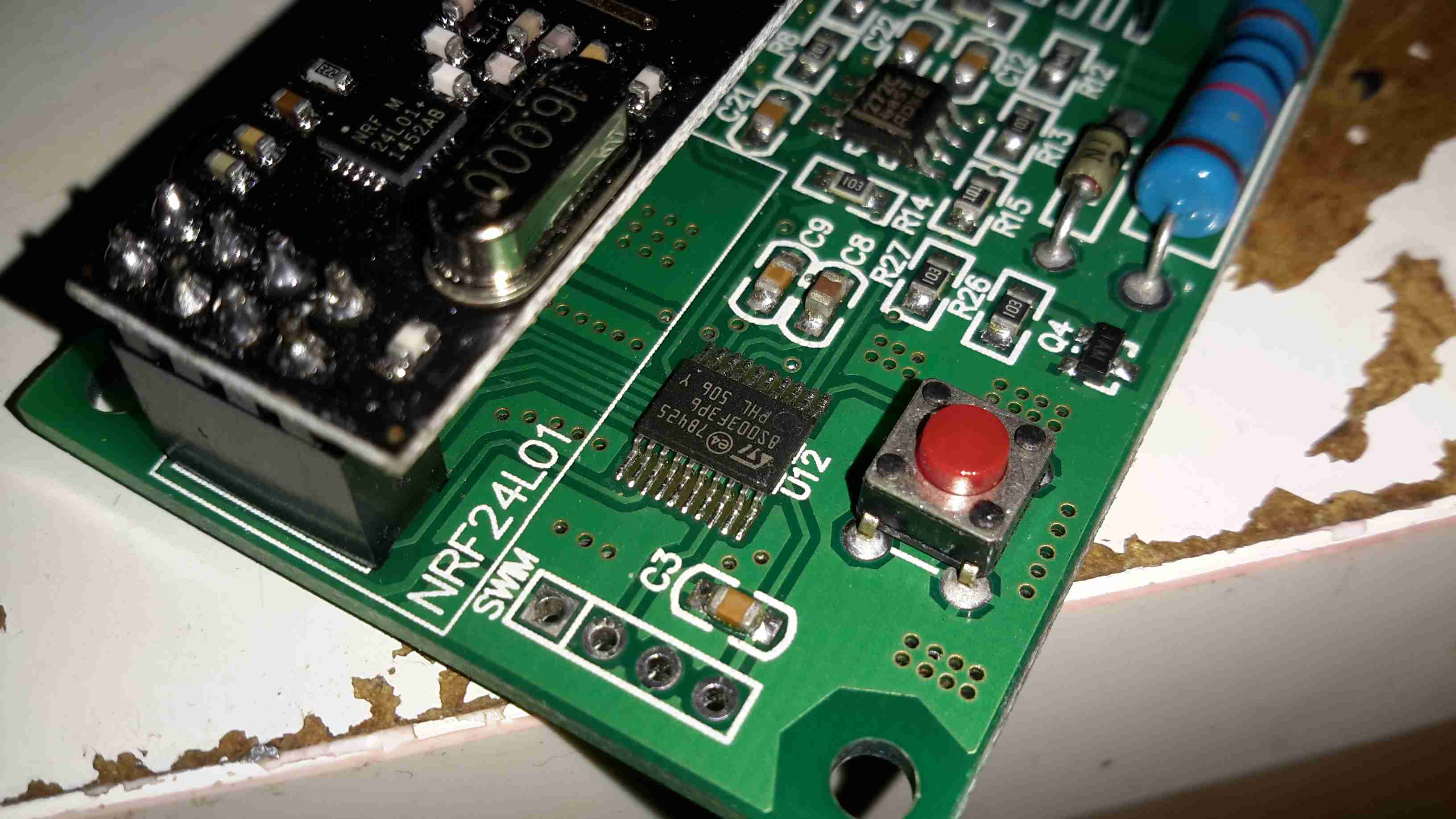
Monitor PCB Microcontroller
The transmitter PCB is controlled with an STM8S003F3 microcontroller from ST Microelectronics. This is a Flash based STM with 8KB of ROM, 1KB of RAM & 10-bit ADC. The NRF24L01 transceiver module is just to the left.
There’s only a single button on this board, for pairing both ends of the link.
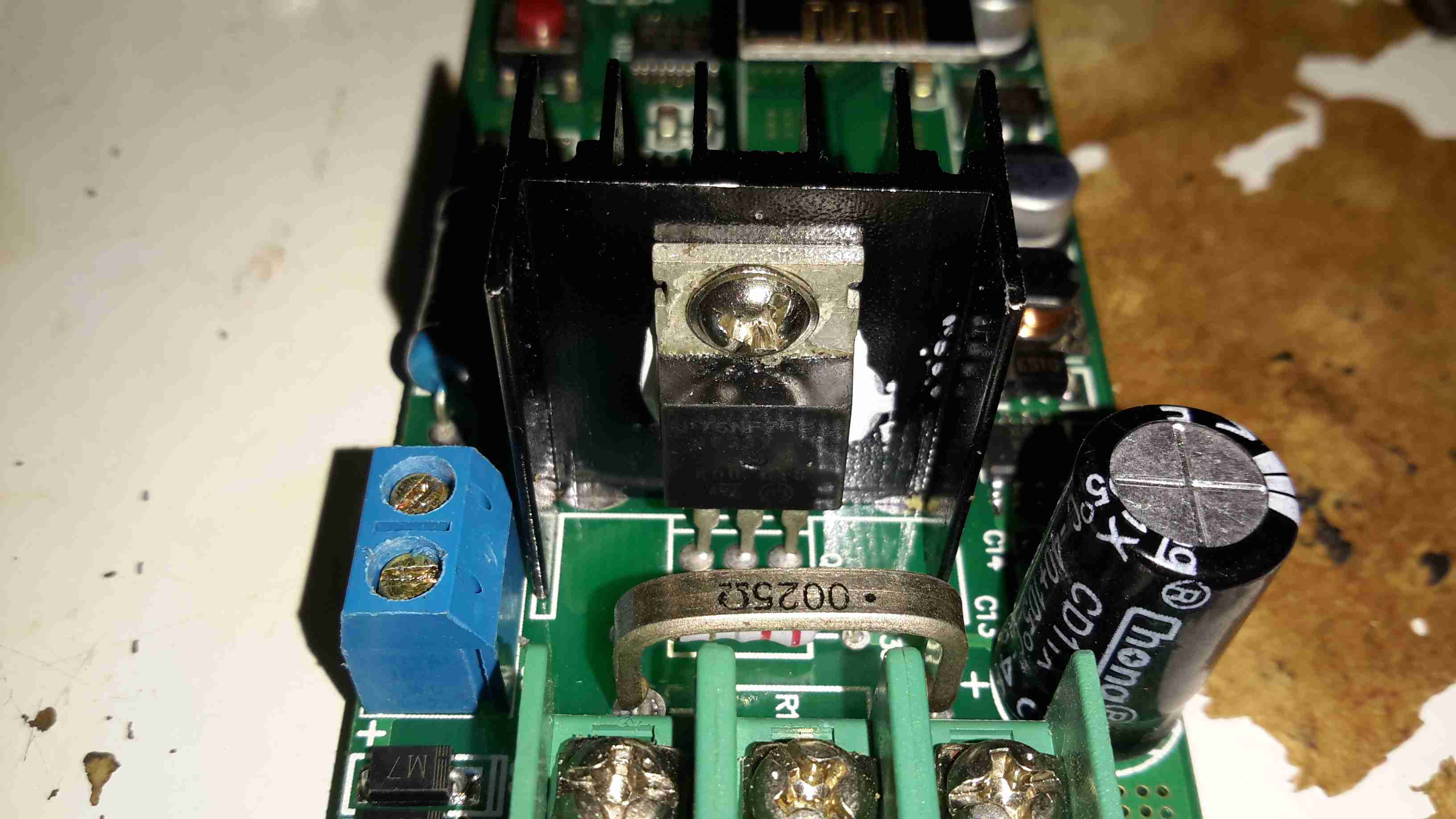
Output MOSFET
The high current end of the board has the 0.0025Ω current shunt & the output switch MOSFET, a STP75NF75 75v 75A FET, also from ST Microelectronics. A separate power source can be provided for the logic via the blue terminal block instead of powering from the source being measured.
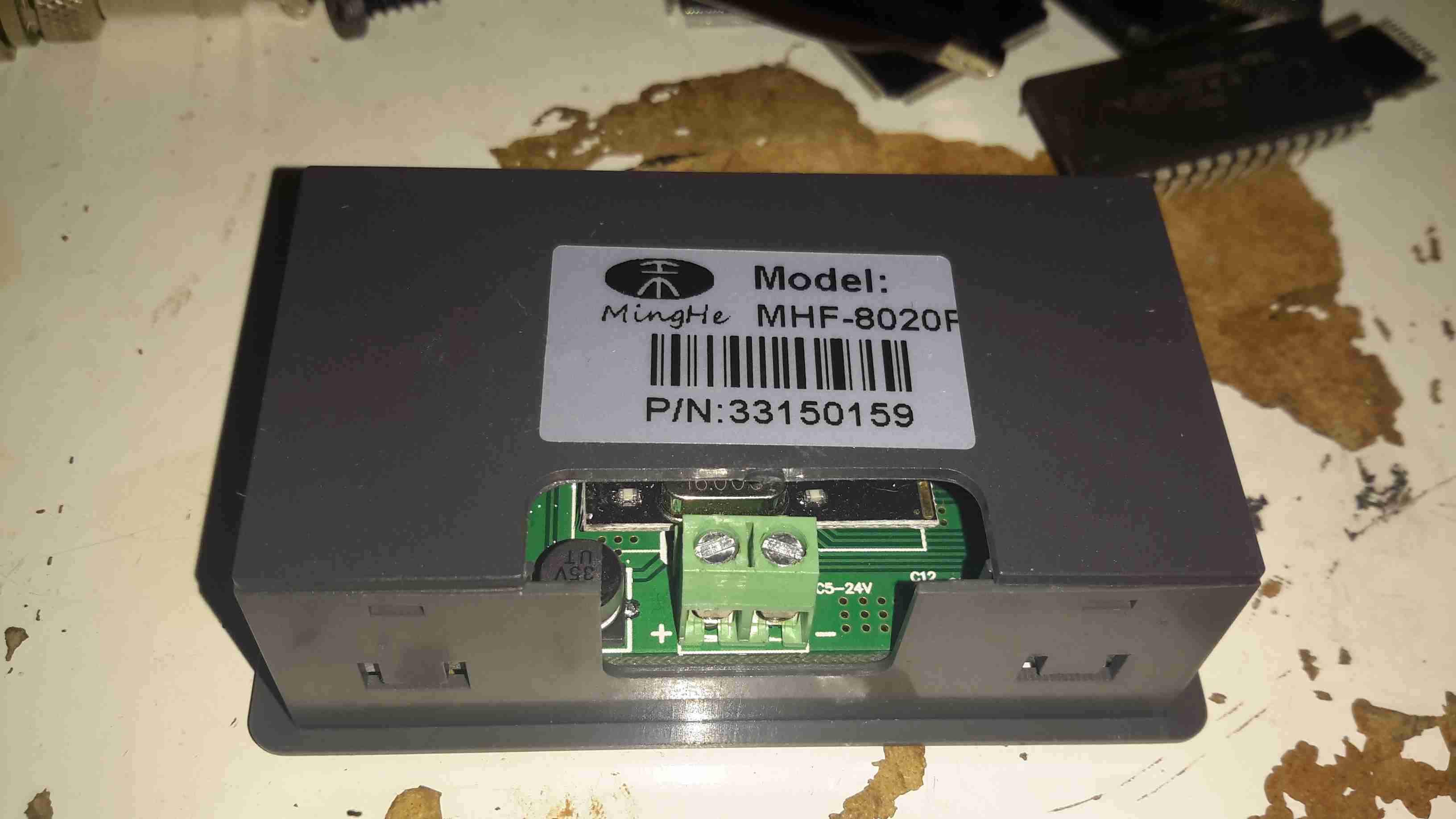
LCD Unit Rear
Here’s the display unit, only a pair of power terminals are provided, 5-24v wide-range input is catered for.
LCD Unit PCB
Unclipping the back of the board reveals the PCB, with another 2.4GHz NRF24L01 module, and a STM8S005K6 microcontroller in this case. The switching power supply that handles the wide input voltage is along the top edge of the board.
Unfortunately I didn’t get any instruction manual with this, so some guesswork & translation of the finest Chinglish was required to get my head round the way everything works. To make life a little easier for others that might have this issue, here’s a list of functions & how to make them work.
LCD Closeup
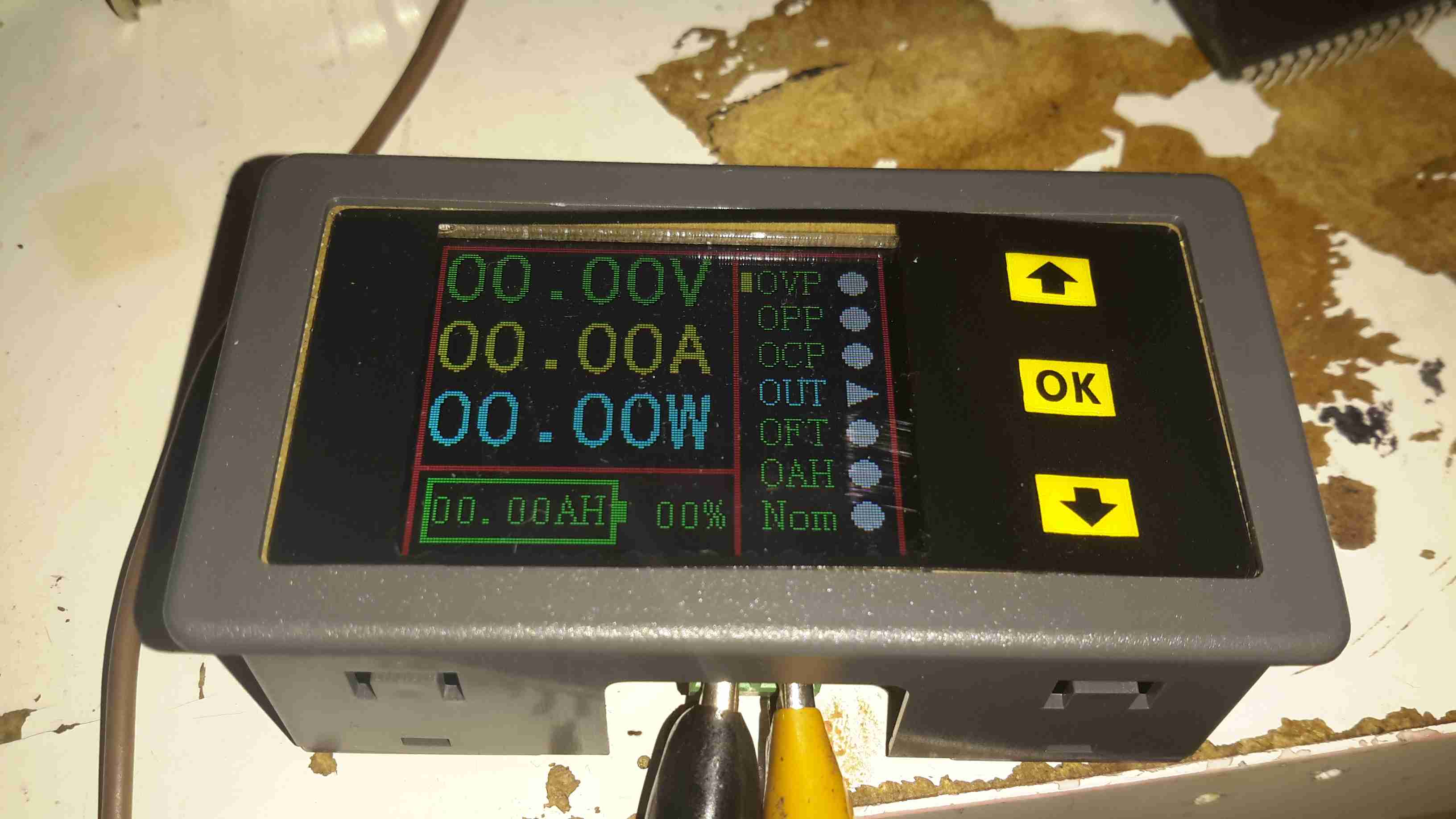
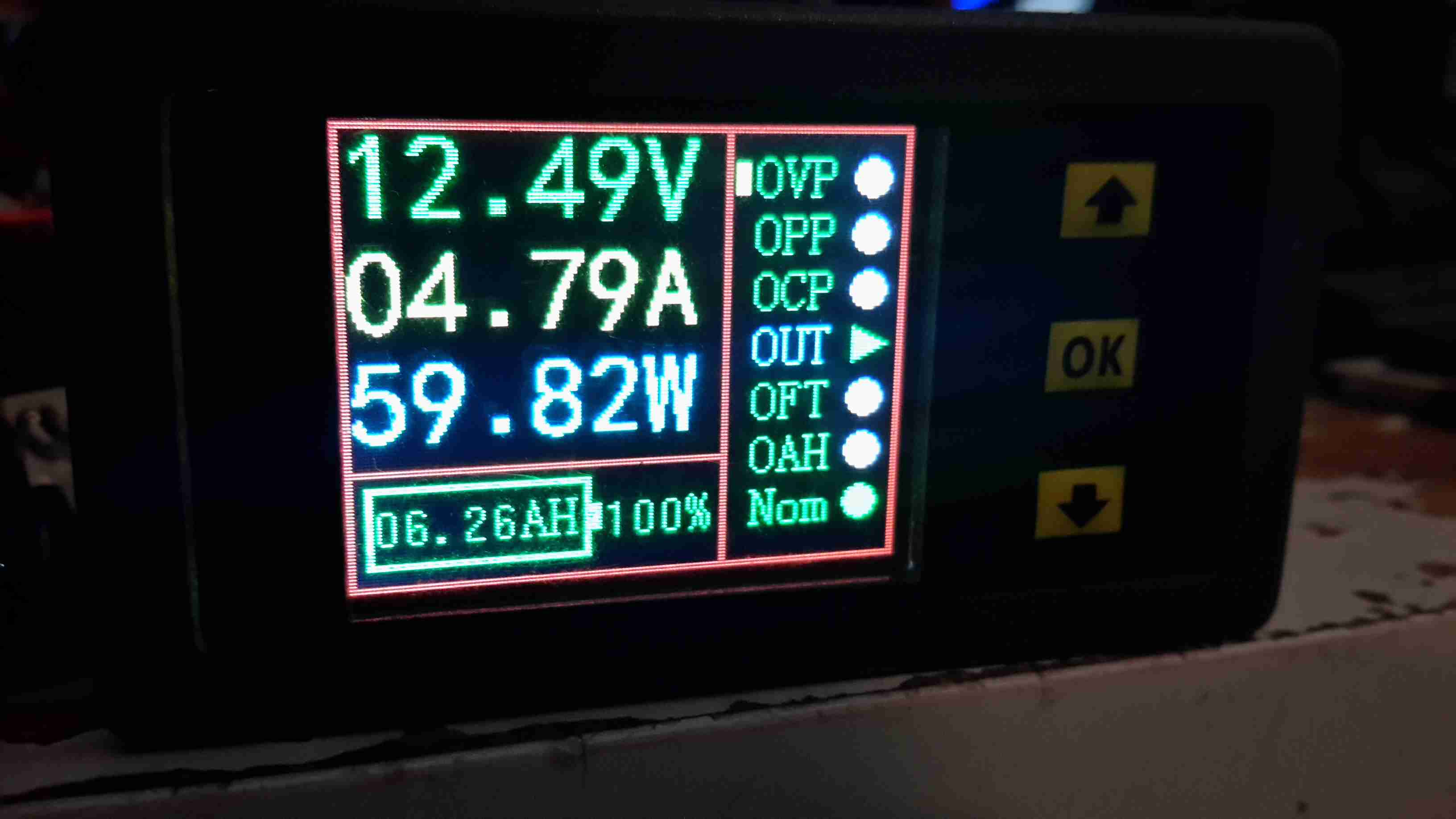
On the right edge of the board is the function list, a quick press of the OK button turns a function ON/OFF, while holding it allows the threshold to be set.
When the output is disabled by one of the protection functions, turning that function OFF will immediately enable the output again.
The UP/DOWN buttons obviously function to select the desired function with the cursor just to the left of the labels. Less obviously though, pressing the UP button while the very top function is selected will change the Amp-Hours display to a battery capacity icon, while pressing DOWN while the very bottom function is selected will change the Watts display to Hours.
The round circle to the right displays the status of a function. Green for OK/ON Grey for FAULT/OFF.
OVP: Over voltage protection. This will turn off the load when the measured voltage exceeds the set threshold.
OPP: Over power protection. This function prevents a load from pulling more than a specified number of watts from the supply.
OCP: Over current protection. This one’s a little more obvious, it’ll disable the output when the current measured exceeds the specified limit.
OUT: This one is the status of the output MOSFET. Can also be used to manually enable/disable the output.
OFT: Over time protection. This one could be useful when charging batteries, if the output is enabled for longer than the specified time, the output will toggle off.
OAH: Over Amp-Hours protection. If the counted Amp-Hours exceeds the set limit, the output will be disabled.
Nom: This one indicates the status of the RF data link between the modules, and can be used to set the channel they operate on.
Pairing is achieved by holding the OK button, selecting the channel on the LCD unit, and then pressing the button on the transmitter board. After a few seconds, (it appears to scan through all addresses until it gets a response) the display will resume updating.
This function would be required if there are more than a single meter within RF range of each other.
I’ve not yet had a proper play with all the protection functions, but a quick mess with the OVP setting proved it was very over-sensitive. Setting the protection voltage to 15v triggered the protection with the measured voltage between 12.5v-13.8v. More experimentation is required here I think, but as I plan to just use these for power monitoring, I’ll most likely leave all the advanced functions disabled.
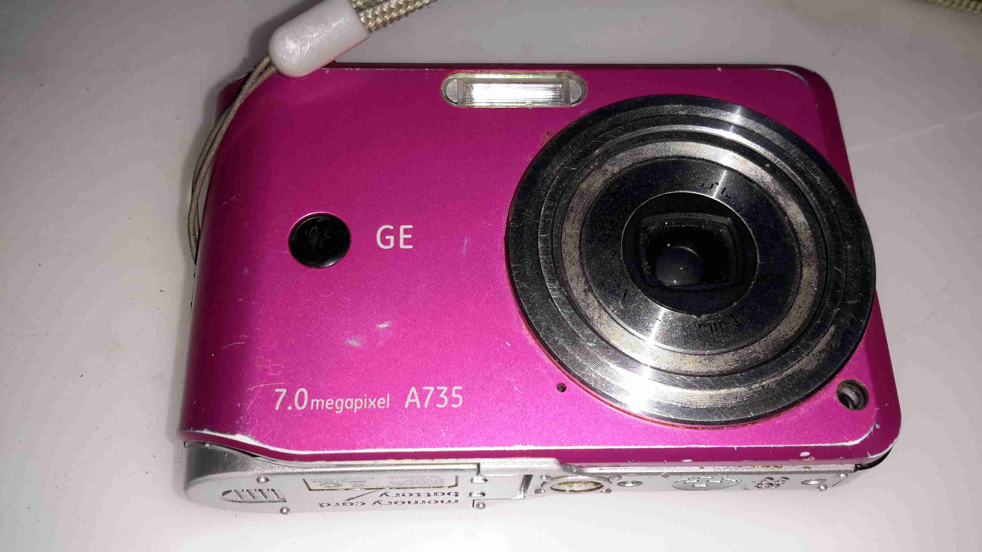
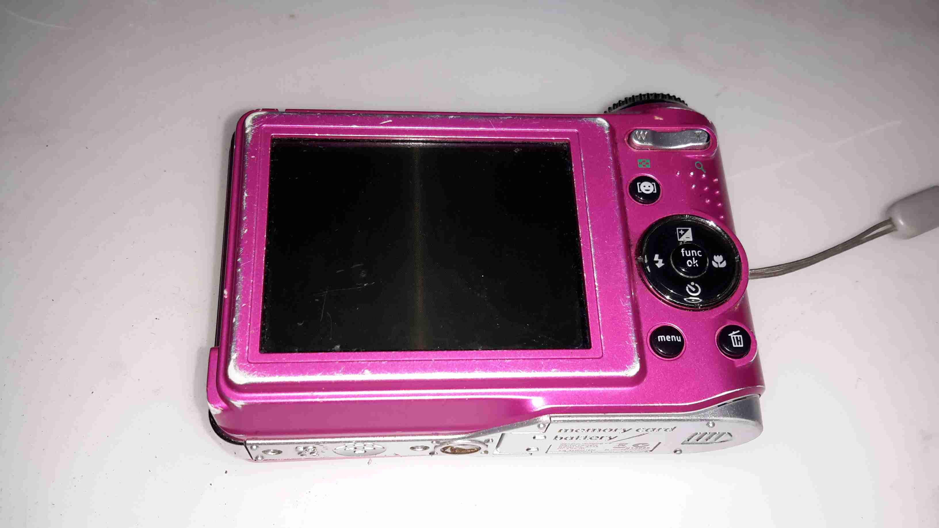
This camera has now been retired after many years of heavy use. Exposure to a 3-year old has caused severe damage to the lens mechanism, which no longer functions correctly.
Rear Panel
Pretty much standard interface for a digital camera, with a nice large LCD for it’s time.
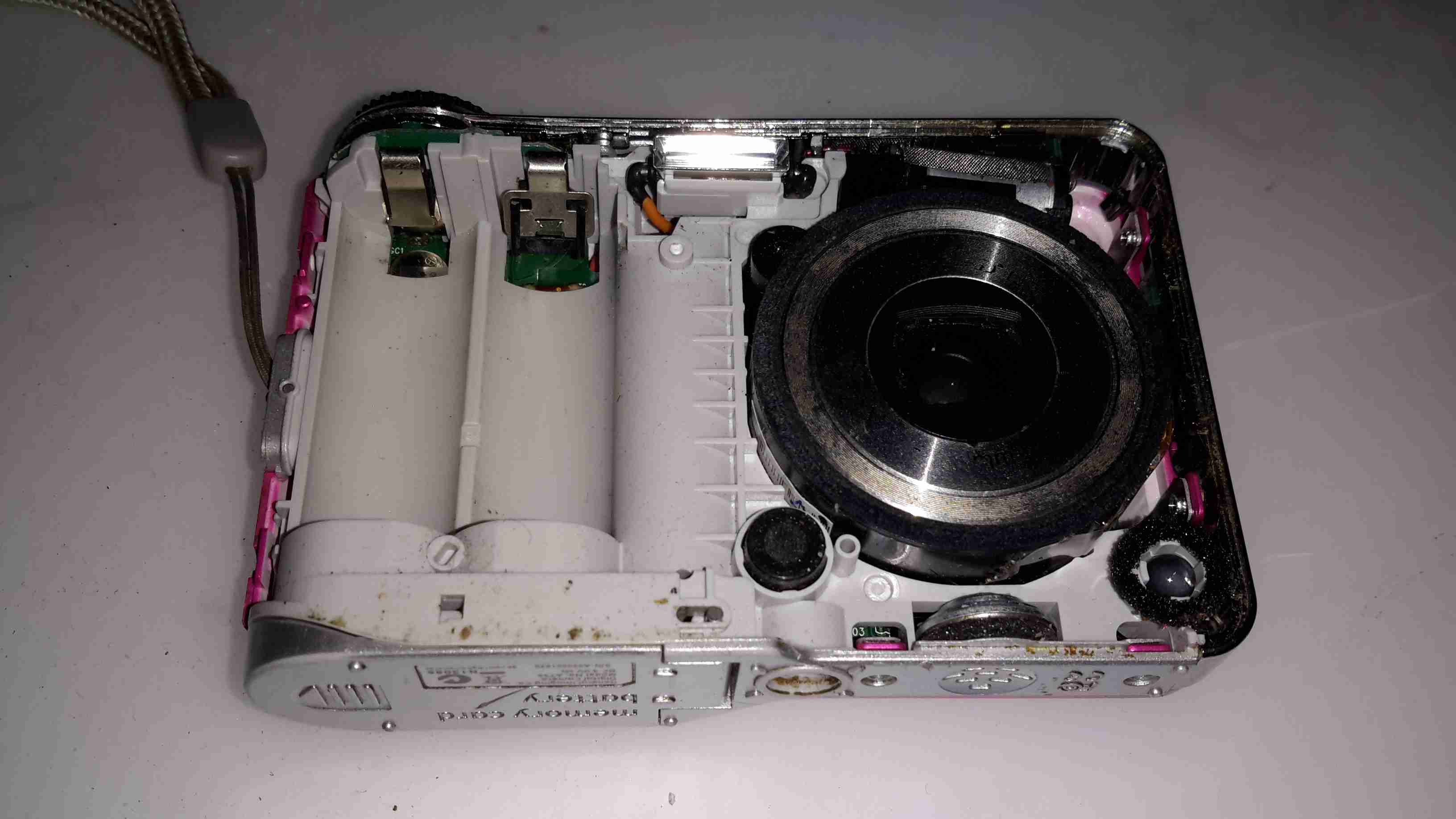
Front Cover Removed
With the front cover removed, the lens assembly & battery compartment is exposed.
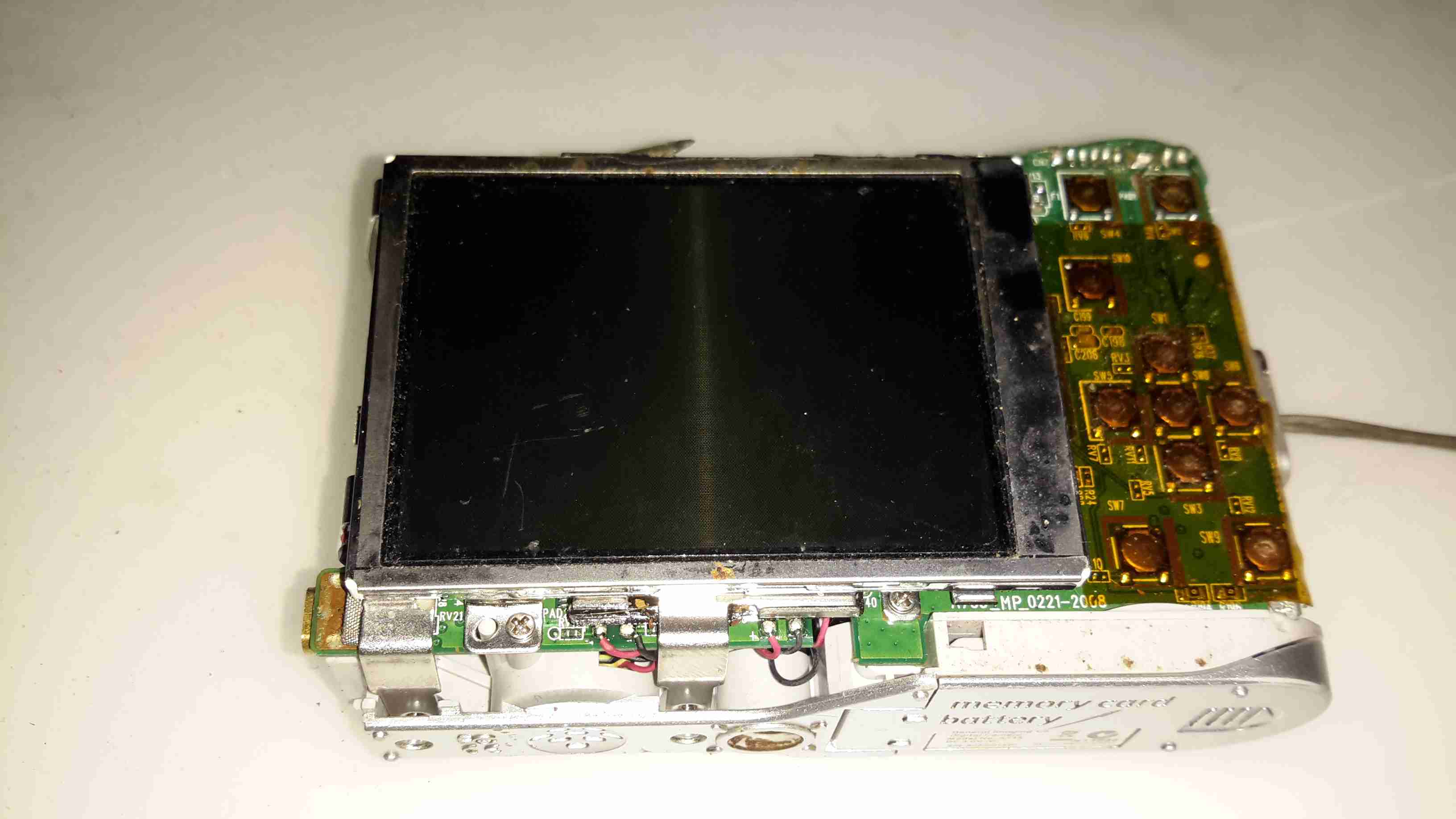
Rear Cover Removed
Removing the rear cover exposes the LCD module & the main PCB, the interface tactile switches are on the right under a protective layer of Kapton tape.
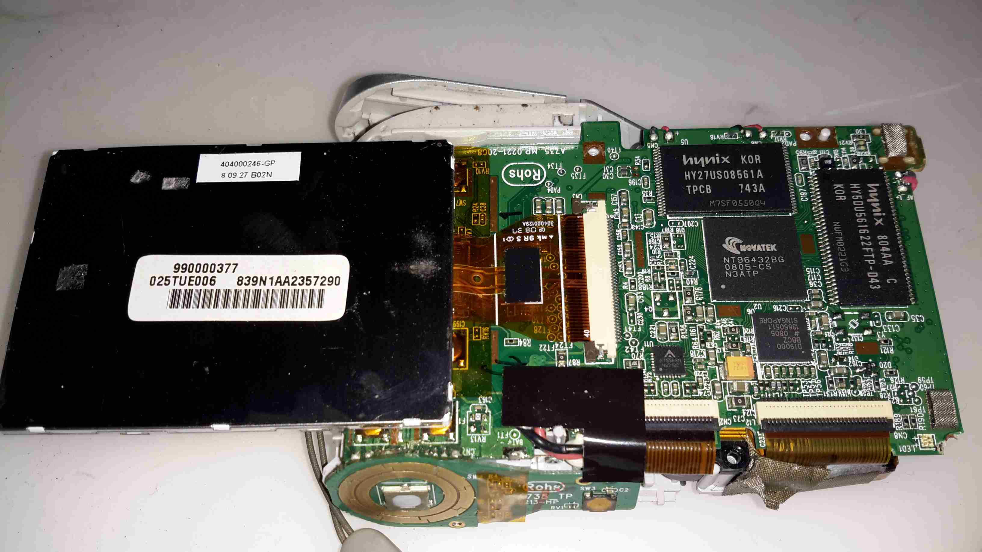
Main Chipset
Flipping the LCD out of it’s mounting bracket reveals the main camera chipset. The CPU is a NovaTek NT96432BG, no doubt a SoC of some kind, but I couldn’t find any information. Firmware & inbuilt storage is on a Hynix HY27US08561A 256MBit NAND Flash, with a Hynix HY5DU561622FTP-D43 256Mbit DRAM for system memory.
I couldn’t find any info on the other two chips on this side of the board, but one is probably a motor driver for the lens, while the other must be the front end for the CCD sensor input to the SoC.
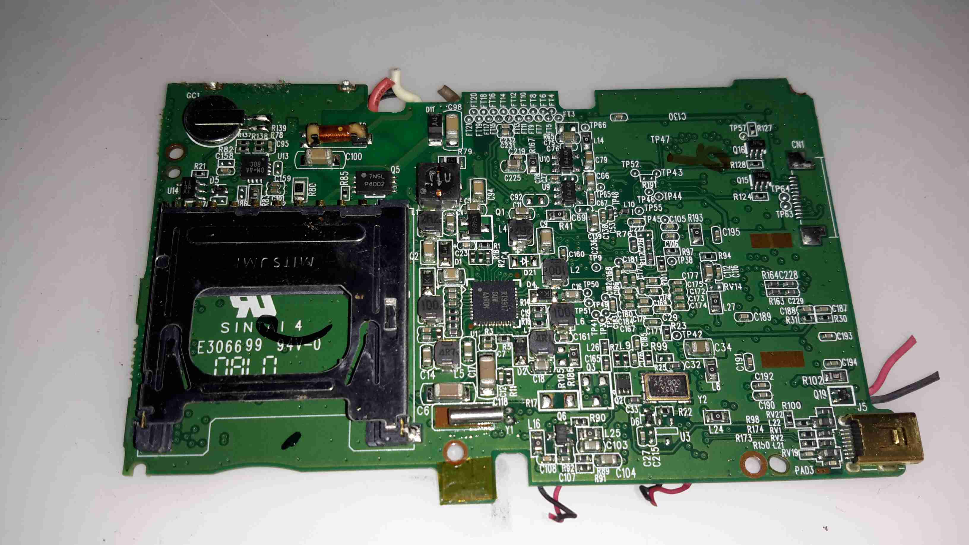
Main PCB Reverse
The other side of the PCB handles the SD card slot & power management. All the required DC rails are provided for by a RT9917 7-Channel DC-DC converter from RichTek, an IC designed specifically for digital camera applications.
Top left above the SD card slot is the trigger circuitry for the Xenon flash tube & the RTC backup battery.
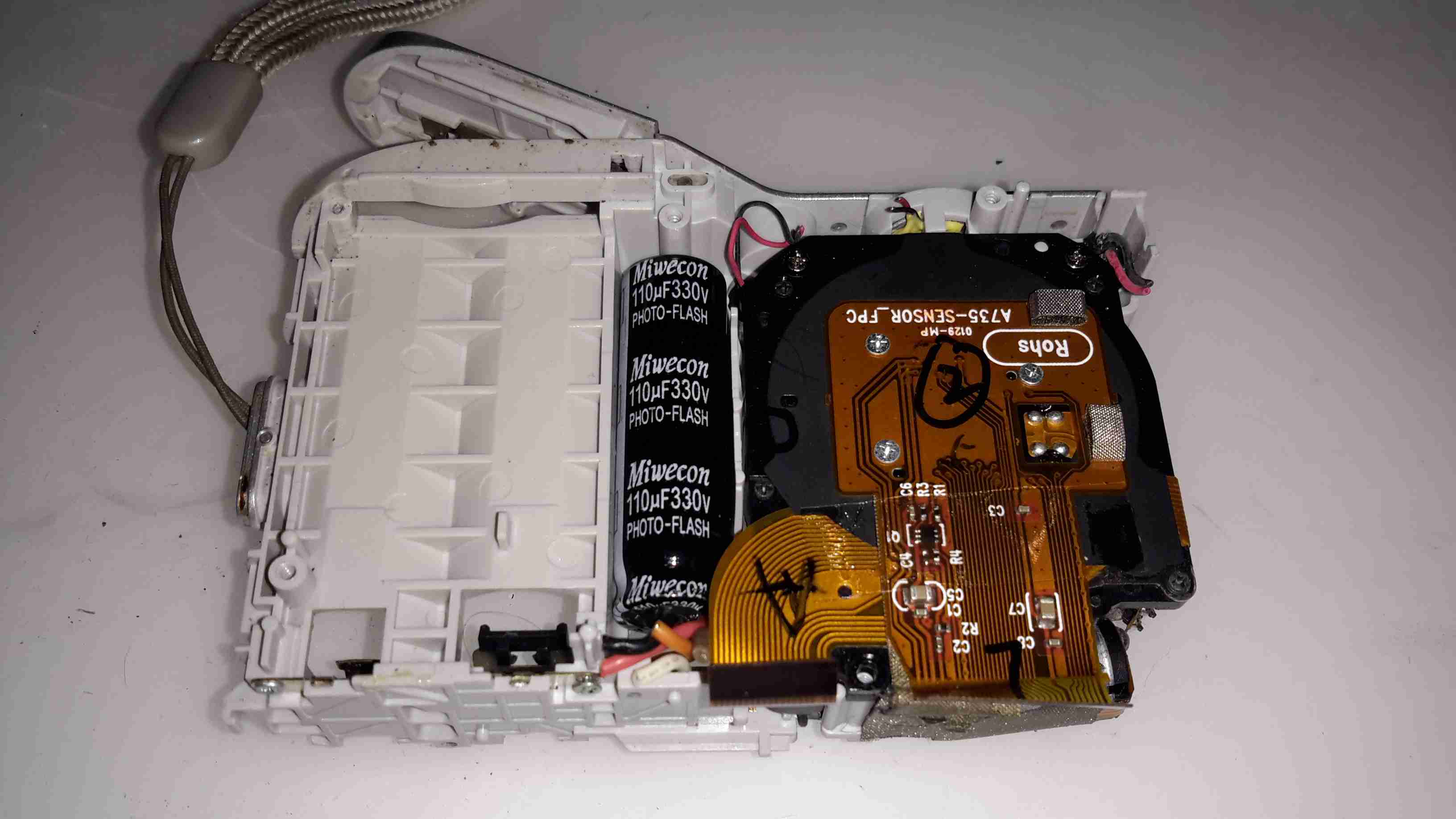
Main PCB Removed
Once the main PCB is out of the frame, the back of the lens module with the CCD is accessible. Just to the left is the high-voltage photoflash capacitor, 110µF 330v. These can give quite the kick when charged! Luckily this camera has been off long enough for the charge to bleed off.
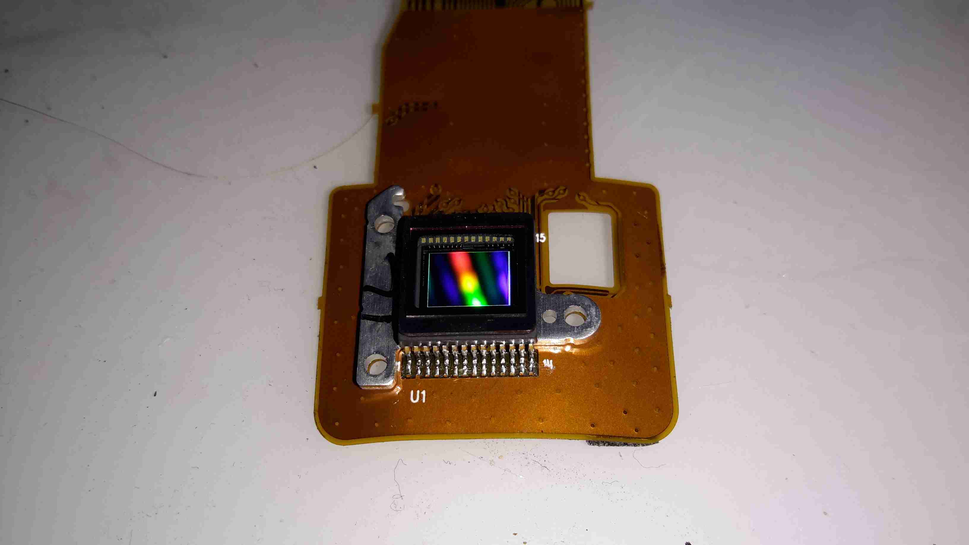
Sensor
Finally, here’s the 7-Megapixel CCD sensor removed from the lens assembly, with it’s built in IR cut filter over the top. I couldn’t find any make or model numbers on this part, as the Aluminium mounting bracket behind is bonded to the back of the sensor with epoxy, blocking access to any part information.
Die images of the chipset to come once I get round to decapping them!
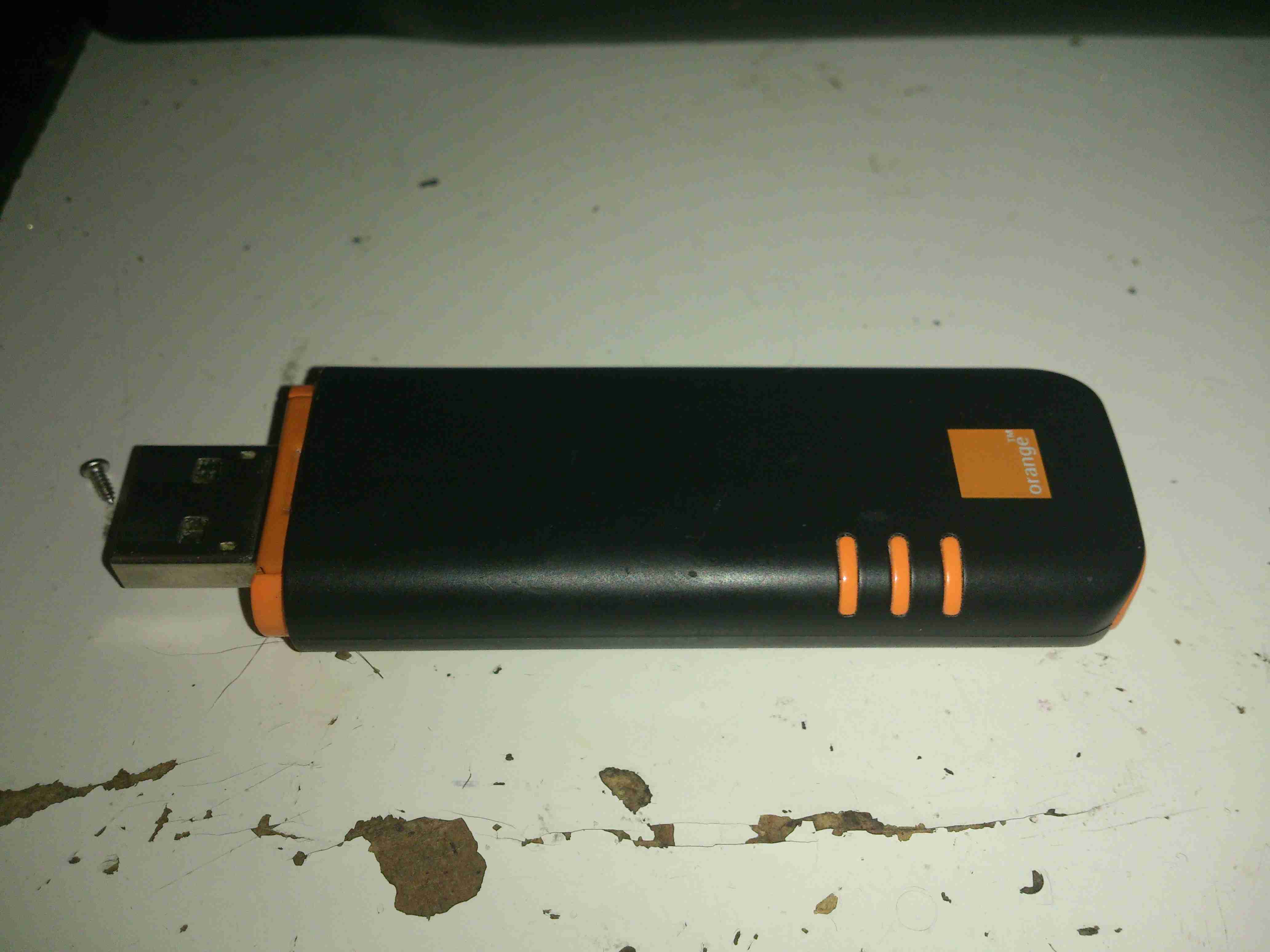
Here’s an old HDSPA 3G USB modem stick that I got with a mobile phone contact many years ago. As it’s now very old tech, and I have a faster modem, not to mention that I’m no longer with Orange (Robbing <expletive>), here’s a teardown of the device!
Cover Removed
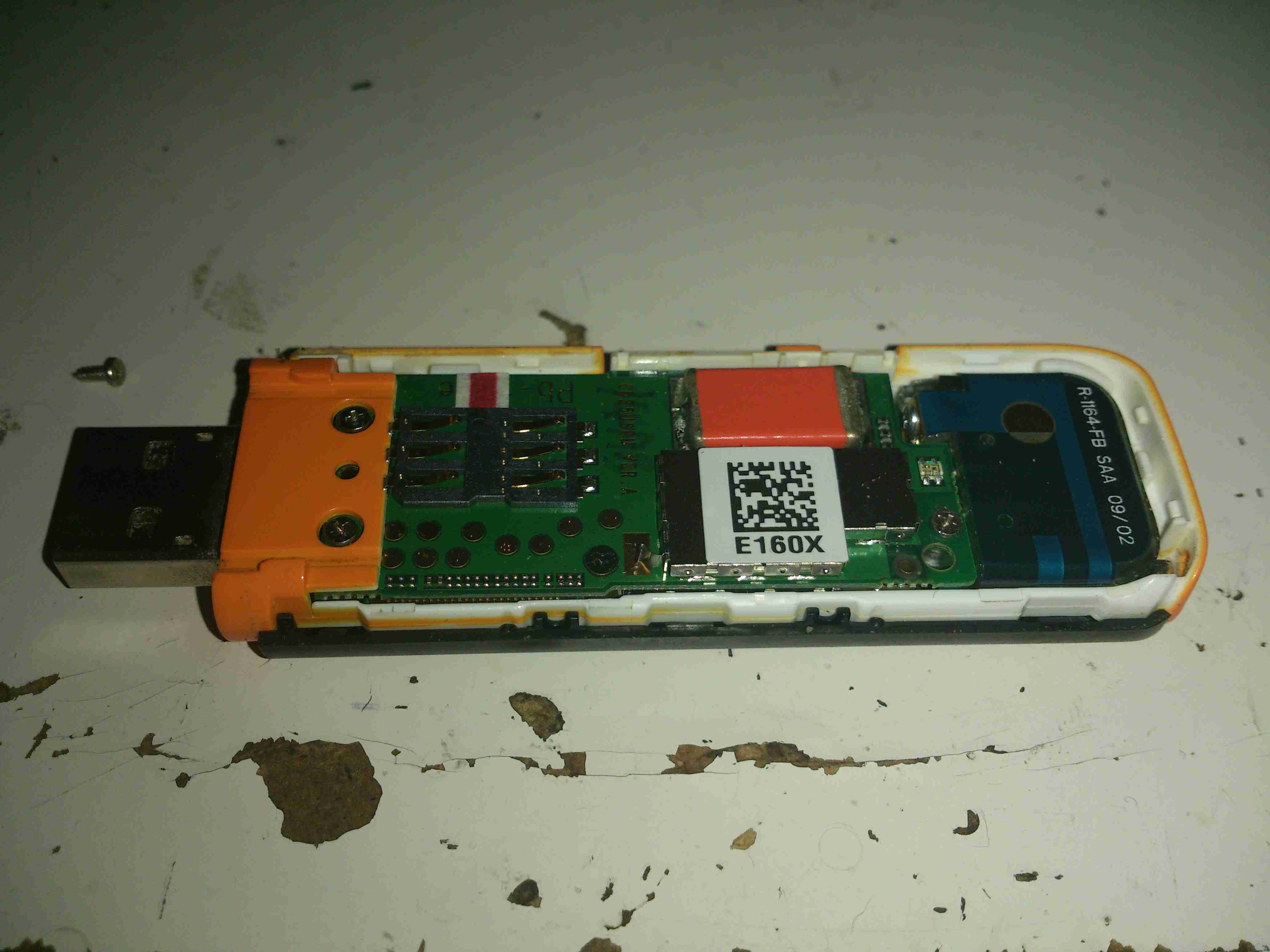
The top shell is just clipped into place, while a pair of very small screws hold down the orange piece at left to hold the PCB stack in the casing. Not much to see here, but it’s clear that there’s a lot crammed into a very small space.
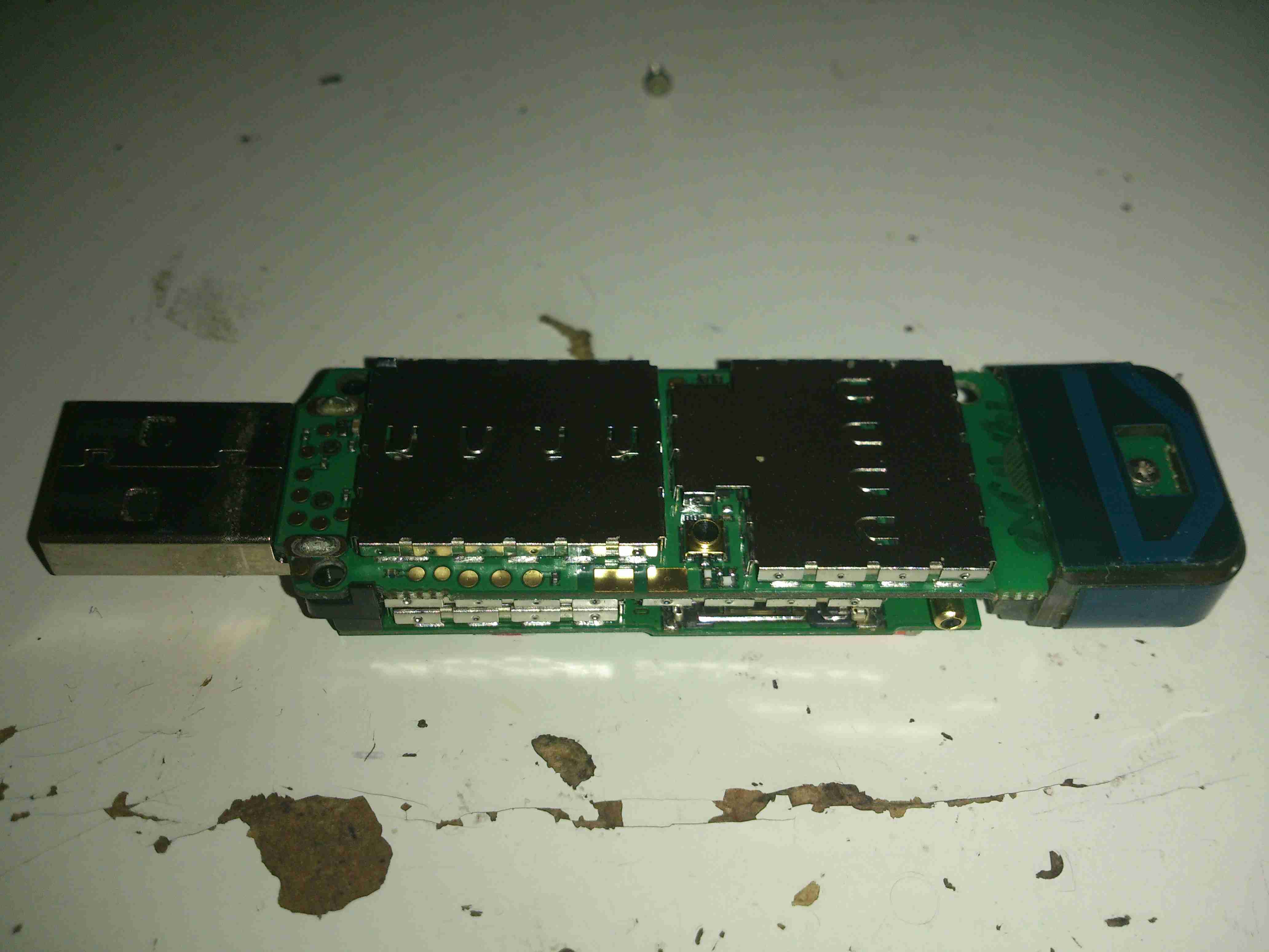
PCB Assembly
Here’s the PCB stack removed from the outer casing. The main antenna is on the right, attached with another small screw. Every IC on the boards is covered with an RF can. No problems there, pliers to the rescue!
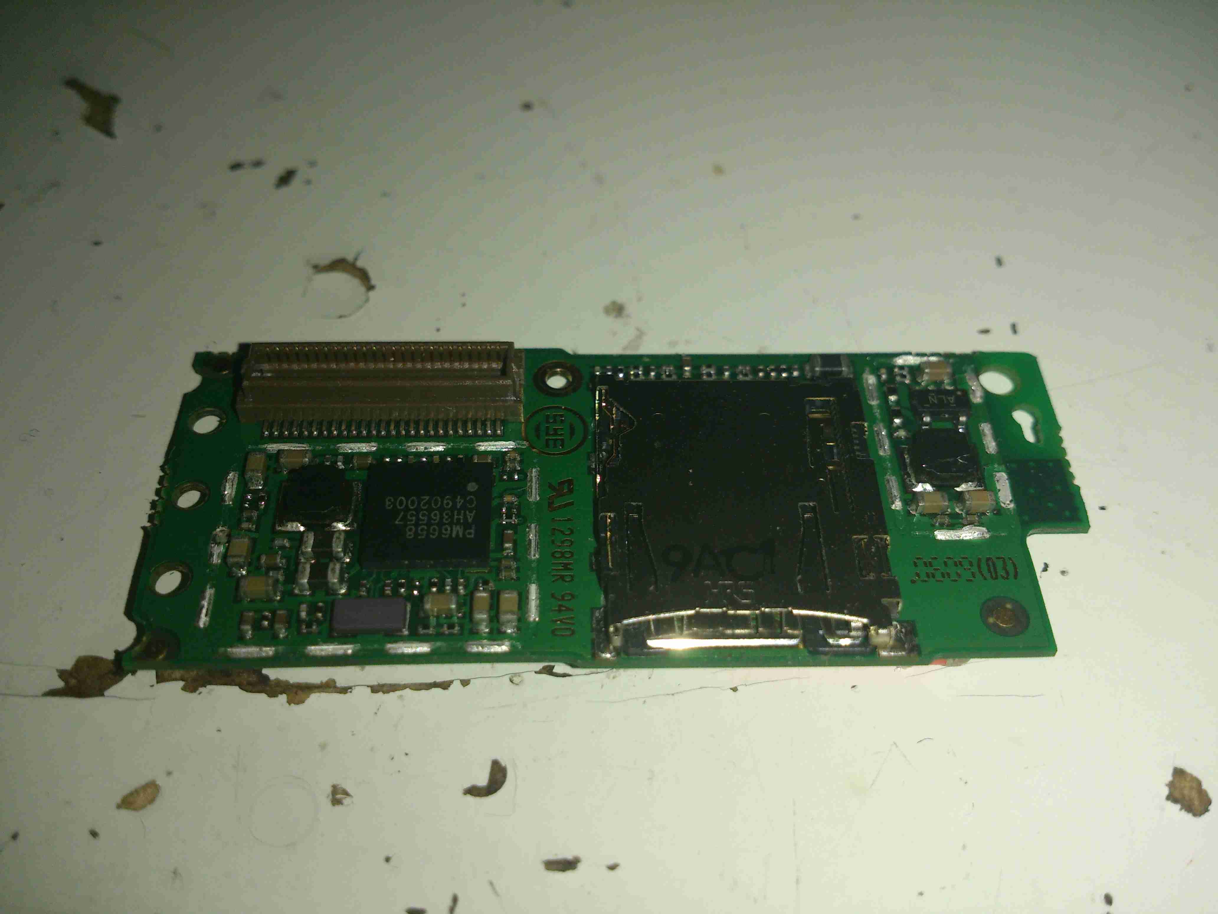
SD Card Slot
Here’s the top PCB, all the shields have been removed. On the left is a Qualcomm PM6658 Power Management IC with integrated USB transceiver. This is surrounded by many of the power management circuits.
The integrated SD Card slot is on the right side. with what looks to be a local switching regulator for supply voltage. This might also provide the SIM card with it’s power supply.
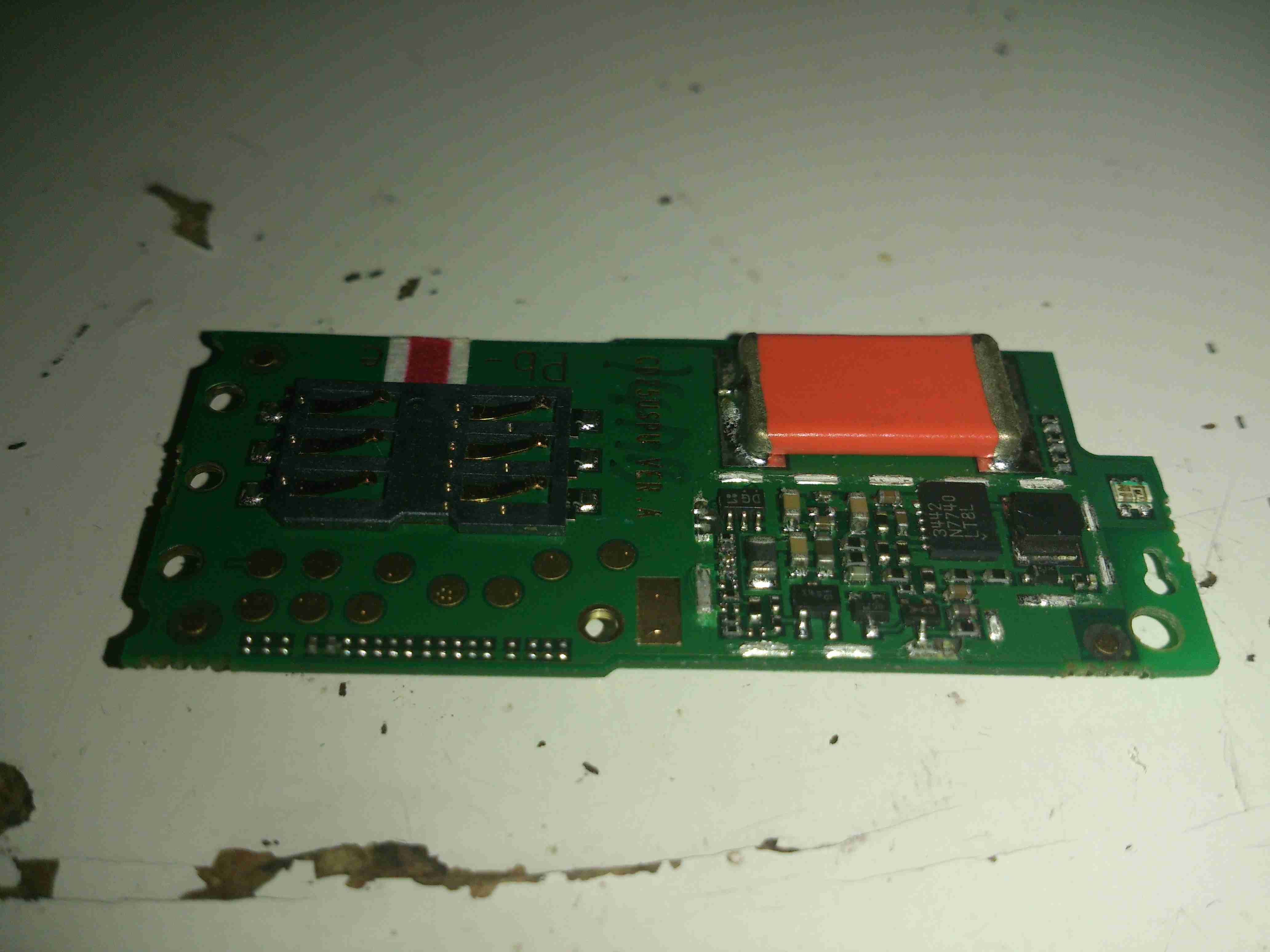
PSU & SIM Contacts
The other side of the top board reveals more power management, with another switching regulator, and a truly massive capacitor at the top edge. I’m guessing this is a solid Tantalum.
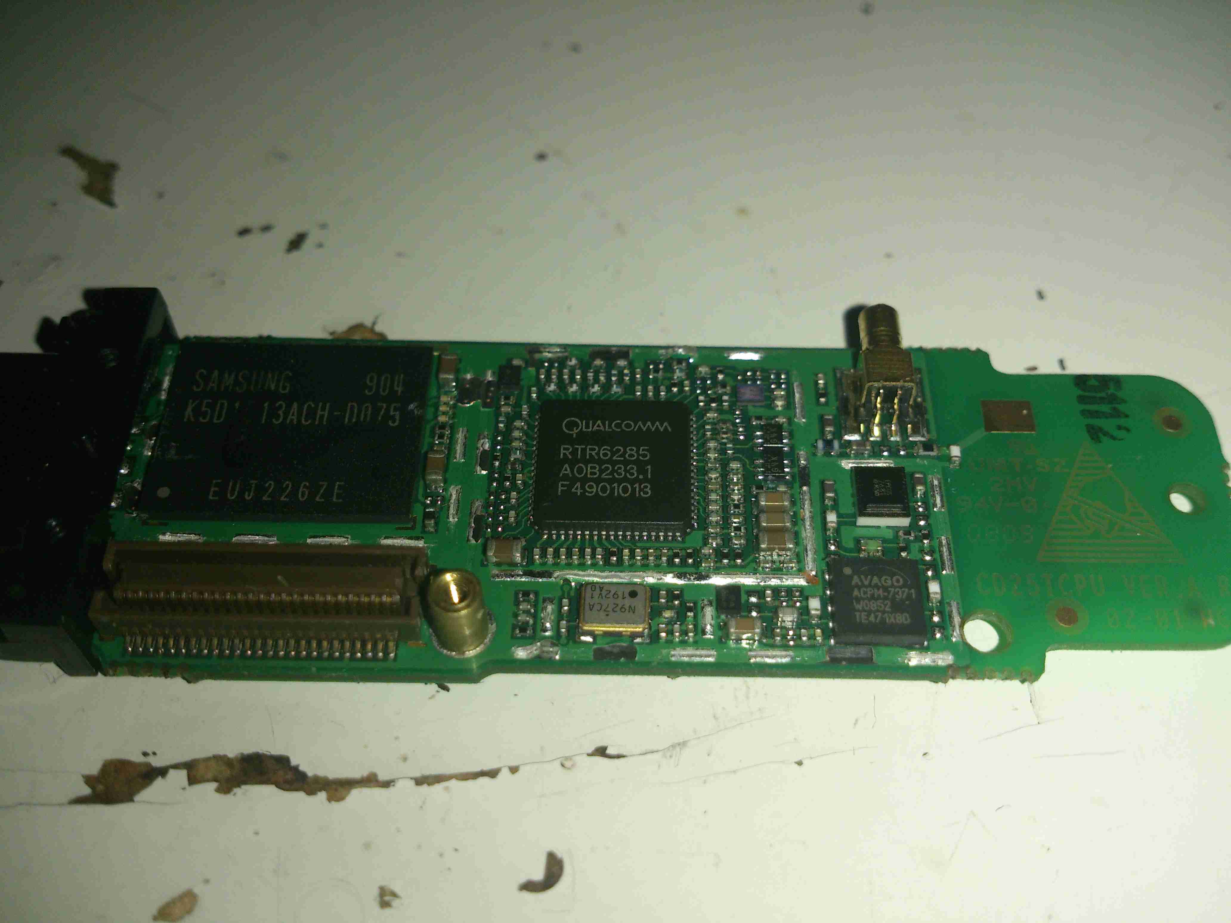
Main Chipset PCB
The other PCB holds the main chipset & RF circuits. On the left here is a Samsung MCP K5D1G13ACH IC. This one is a multiple chip package, having 1Gbit of NAND Flash & 512Mbit of mobile SDRAM.
To it’s right is a Qualcomm RTR6285 RF Transceiver. This IC supports multiband GSM/EDGE/UMTS frequencies & also has a GPS receive amplifier included.
At bottom right is an Avago ACPM7371 Wide-Band 4×4 CDMA Power Amplifier. The external antenna connector is top right.
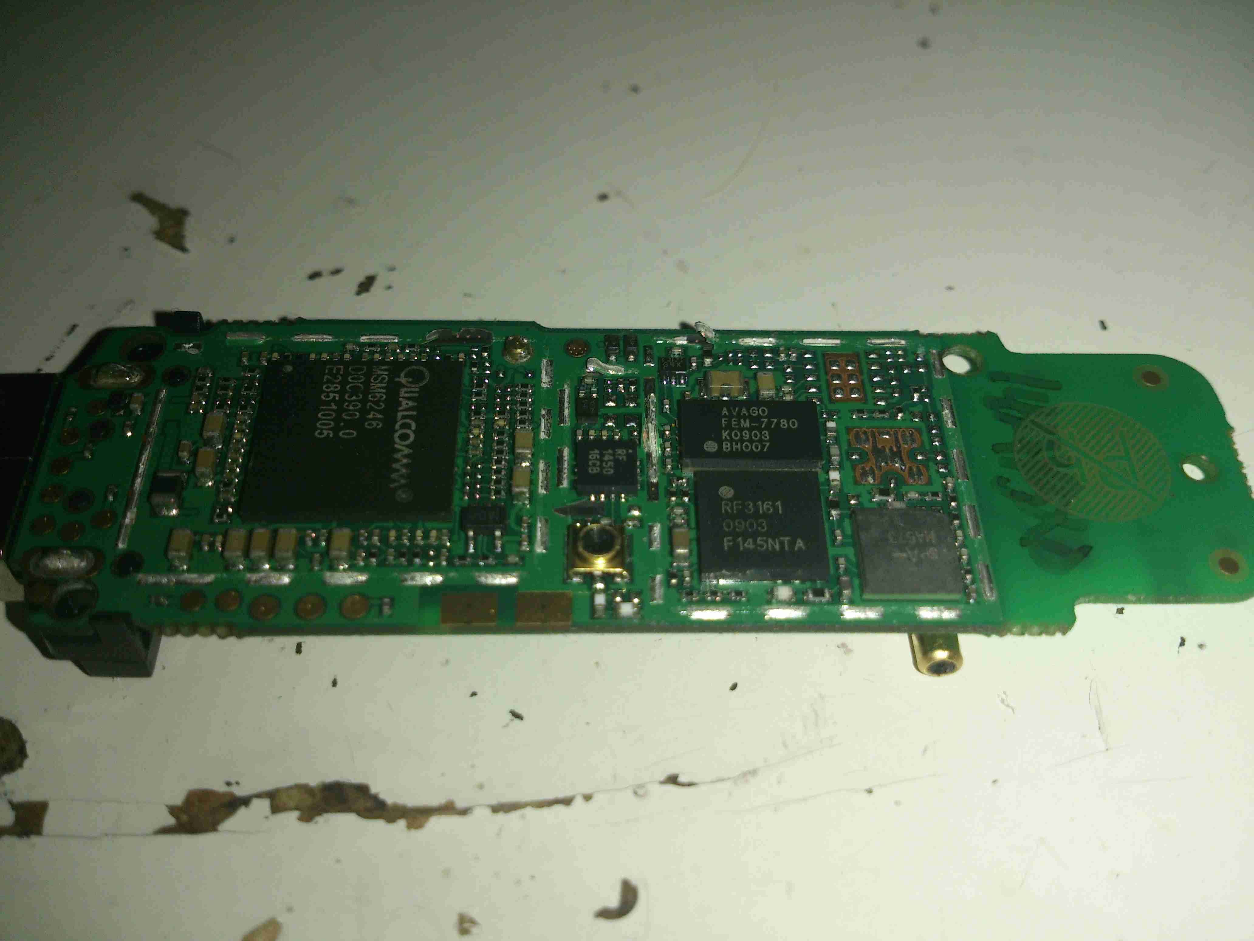
Main Chipset PCB Reverse
On the other side of the main PCB is a Qualcomm MSM6246 Baseband processor. Not sure about this one as I can’t find anything resembling a datasheet. Another micro-coax connector is in the centre, probably for factory test purposes, as it’s not accessible from the outside.
Just above the coax connector is a Qorvo RF1450 SP4T (single-pole 4-throw) High Power (34.5dBm) GSM RF Switch.
Upper right is an Avago FEM-7780 UMTS2100 4×7 Front End Module.
Under that is an RFMD RF3163 Quad-Band RF Power Amplifier Module.
I have yet another receipt printer, this one appears to be brand new. It’s possibly the smallest thermal 80mm printer I have at the moment, and has both USB & Serial interfaces.
Controller PCB
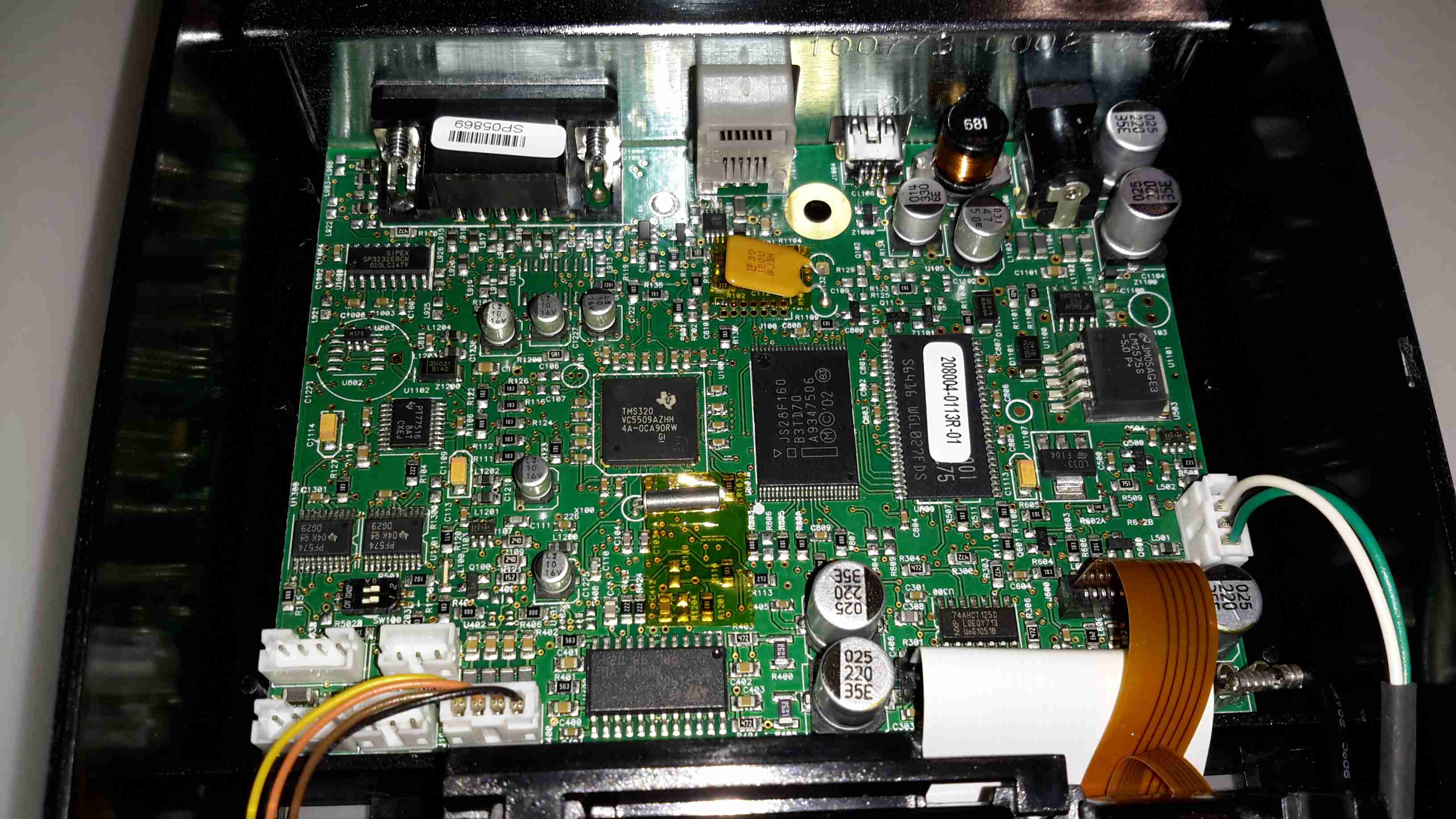
There’s not much to these printers at all. Removing a single screw allows the case halves to separate, showing the guts. The controller is based around a Texas Instruments TMS320VC5509AFixed-Point DSP. It’s associated Flash ROM & RAM are to the right.
Power supply is dealt with in the top right of the PCB, with the interface ports further left.
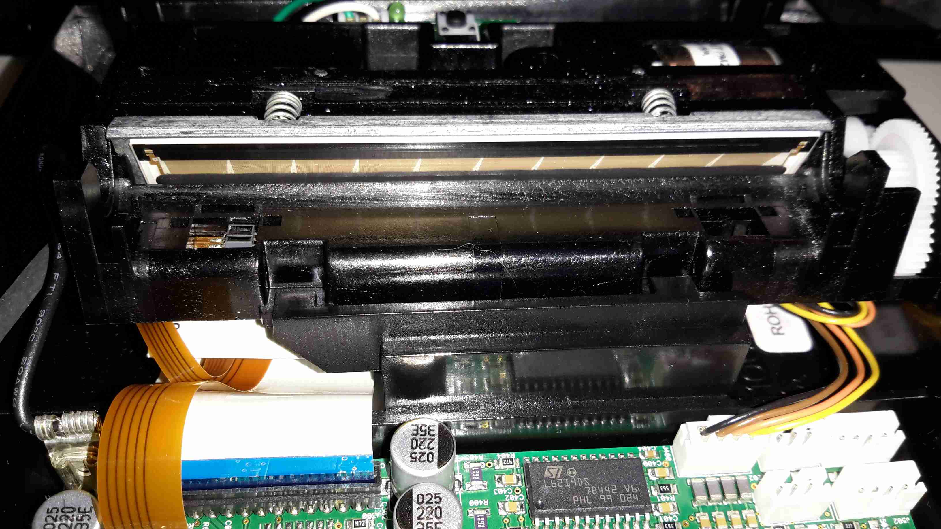
Print Head
Here’s the thermal mechanism itself, with the large print head. The stepper motor to drive the paper through the printer is just peeking out at top right. The paper present sensor is just under the left hand side of the print head.
Everyone at some stage must have seen these EAS security tags in shops, usually attached to clothing with a steel pin. As some of this year’s presents had been left with the tags attached, I had to forcibly remove them before wrapping could commence.
Reverse Side
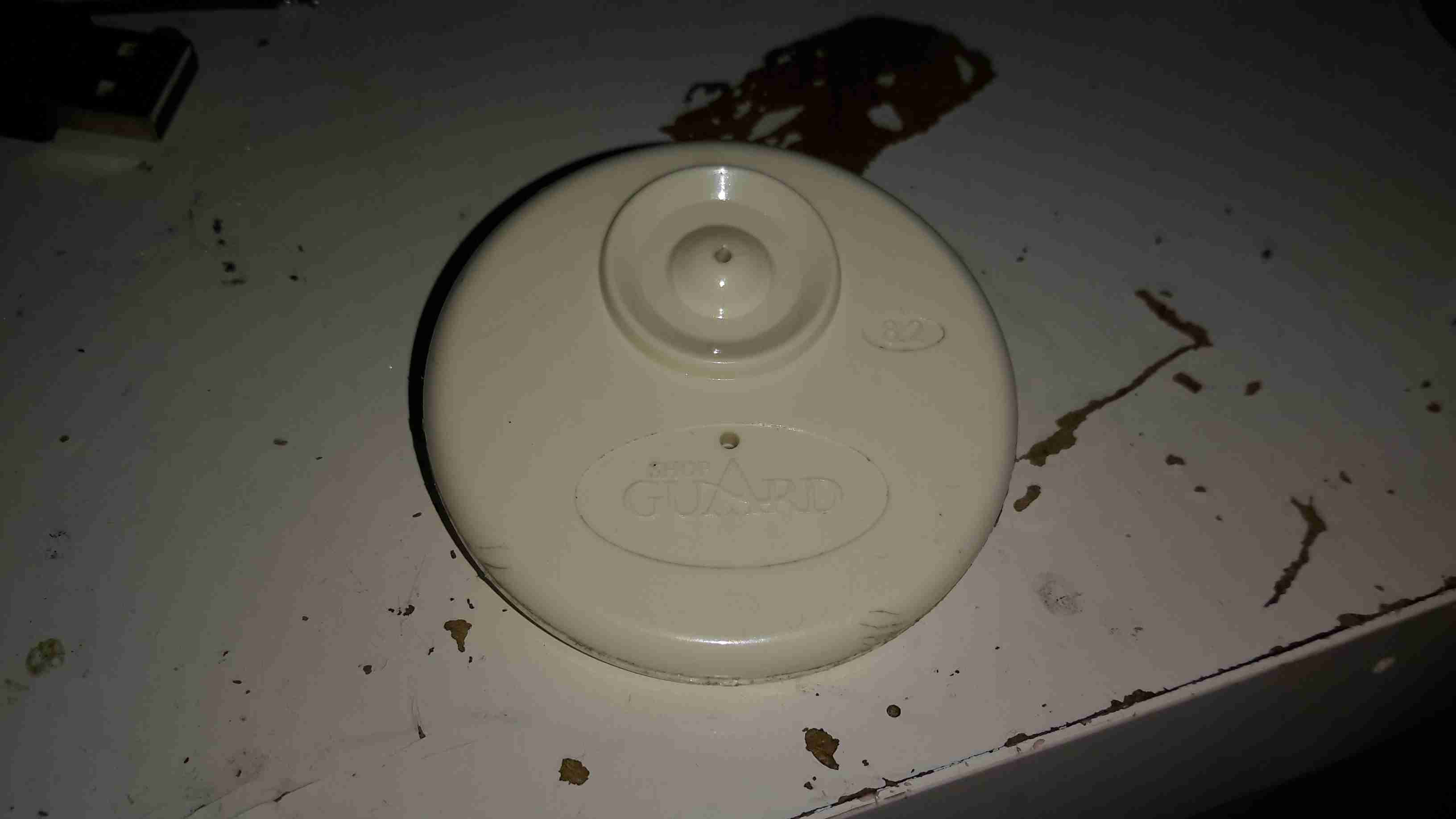
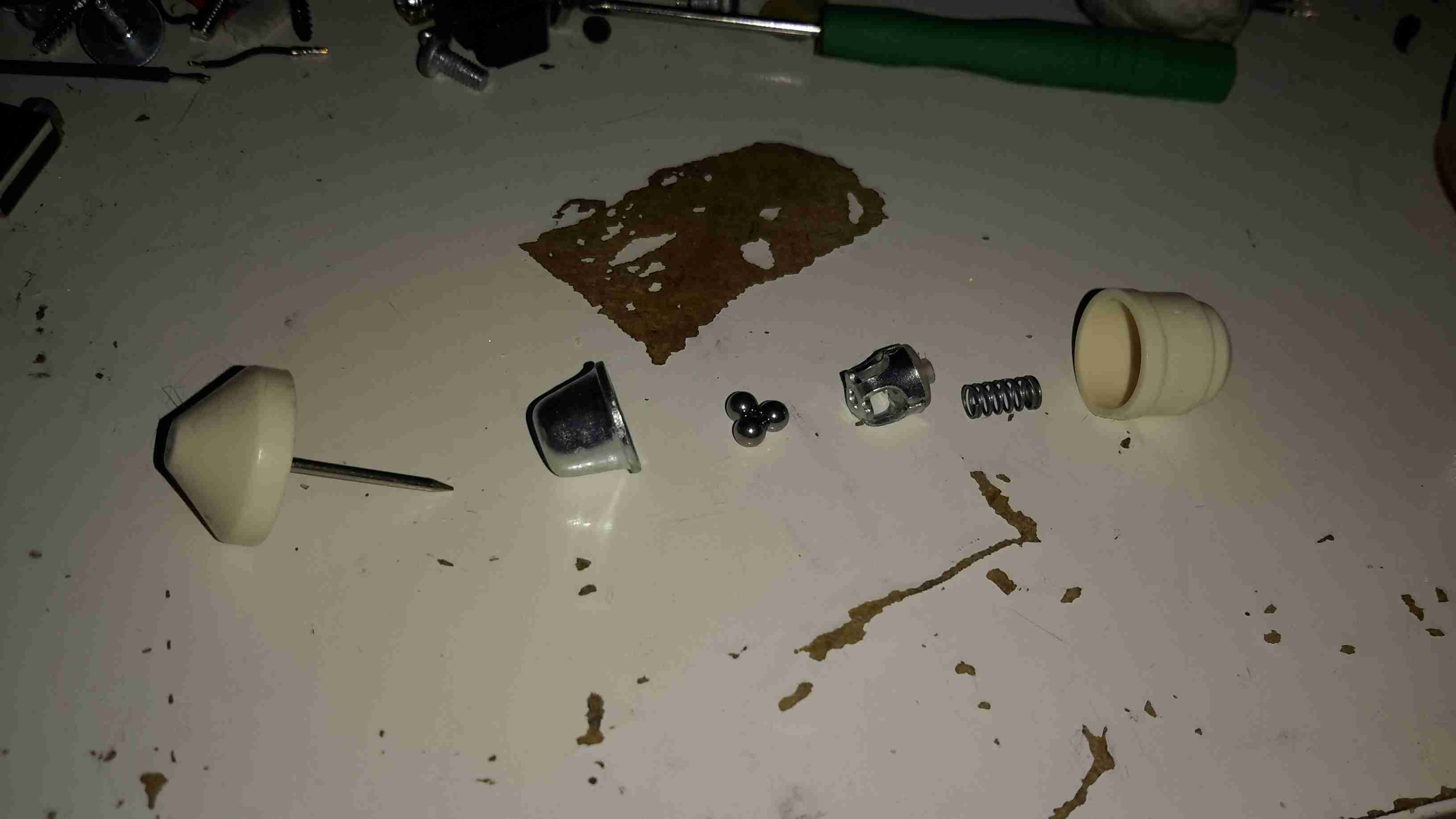
These are just a plastic disc about 50mm in diameter, with an internal locking mechanism & RF tag inside.
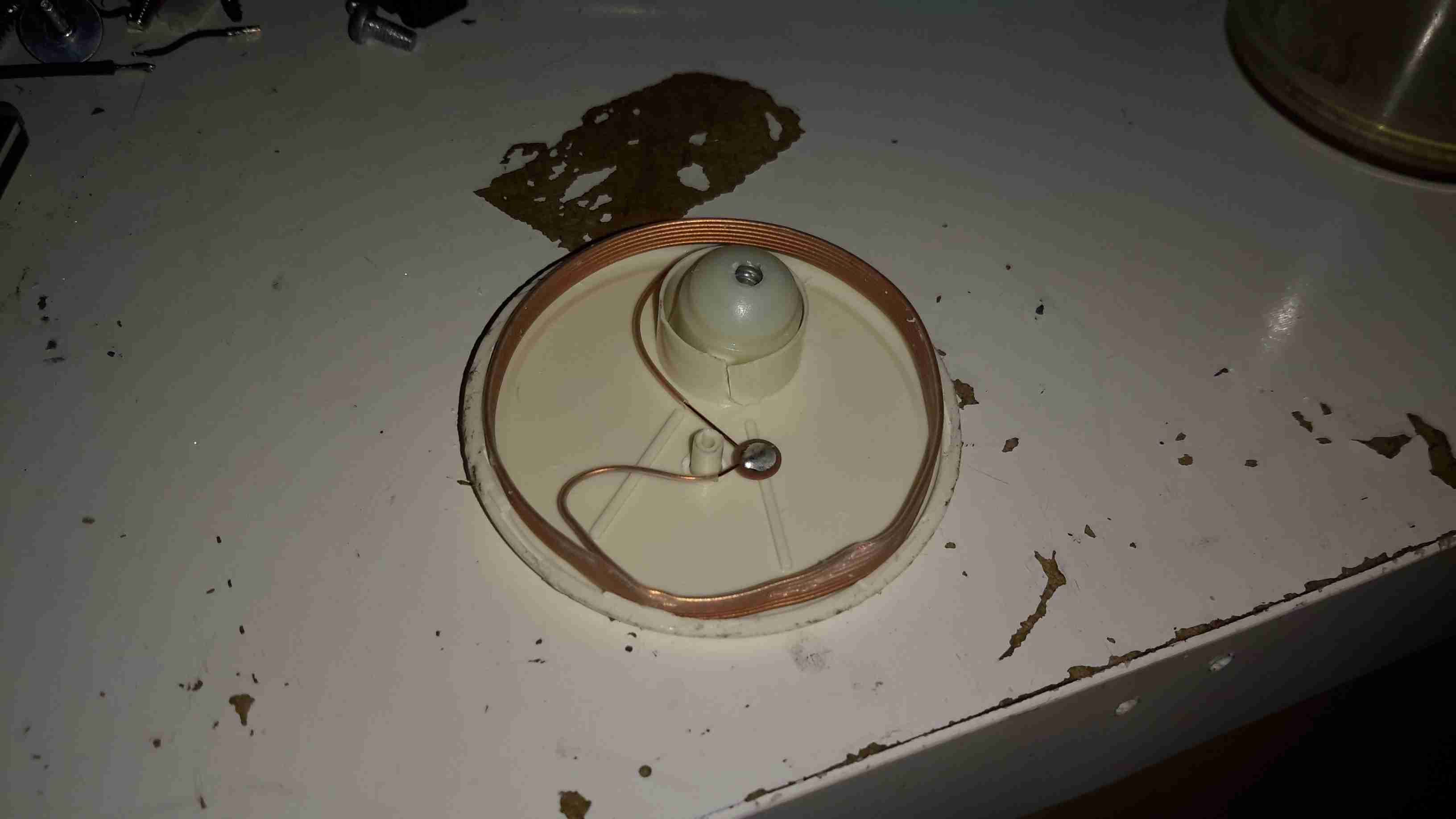
RF Coil
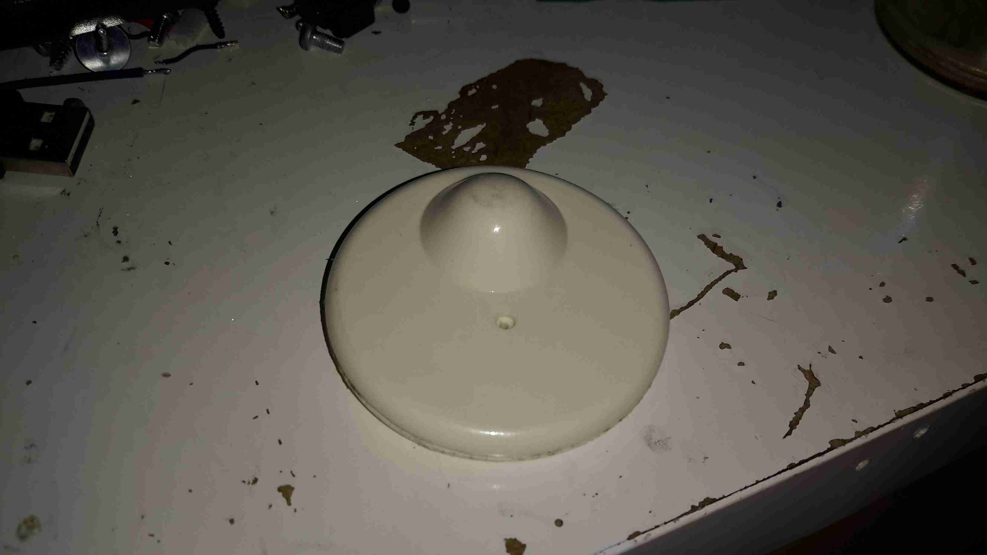
After some careful attack with a saw around the glue seam, the tag comes apart into it’s halves. The RF coil & it’s ceramic capacitor can be seen wrapped around the outside of the tag. The capacitor in this case isn’t even epoxy dipped to save that extra 0.0001p on the manufacturing price. In the top centre is the pin locking mechanism, enclosed in a small plastic pill.
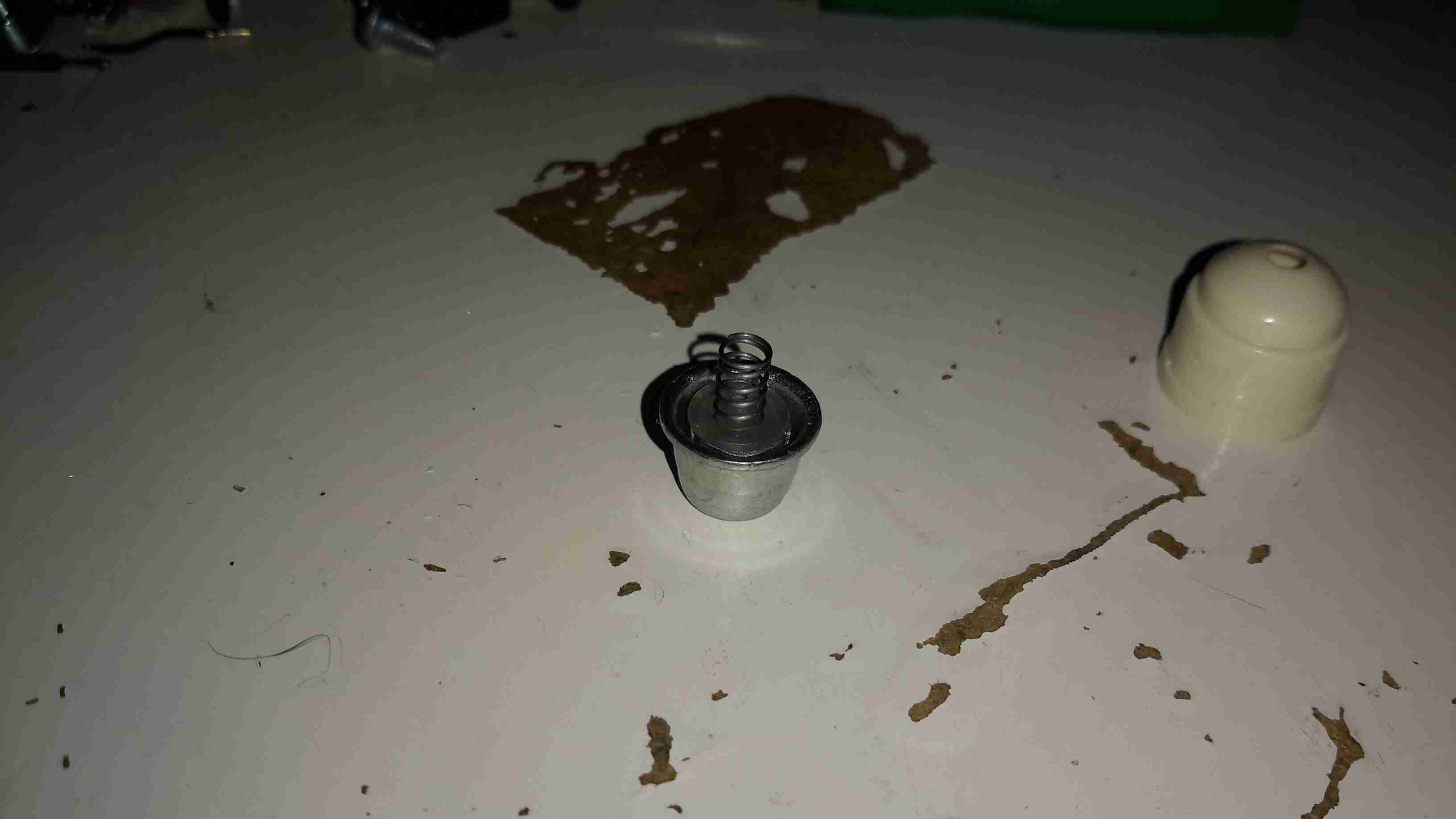
Lock Pill
Popping off the back cap of the lock shows it’s internals.
Ball Bearing Lock Assembly
The lock itself is very simple. The centre section, held in place by a spring, carries 3 small ball bearings. The outer metal frame of the lock is conical in shape.
When the pin is pushed into the tag, the conical shape of the lock chamber causes the ball bearings to grab onto it, helped by the action of the spring that pushes the ball bearing carrier further into the cone.
This also means that any attempt to force the mechanism causes it to lock tighter onto the pin.
In normal operation, removal is achieved by a strong magnet that pulls the ball bearing carrier back slightly against it’s spring, allowing the pin to disengage & be pulled out.
This design is incredibly simple & cheap to make, and gains it’s locking strength from friction alone.
I would consider the RF coil being around the outer edge of the device a bit of a security risk – a quick chop with a sharp pair of wire cutters would disable the tag’s alarm functionality instantly. Making the coil slightly smaller & keeping it out of reach of the edge of the tag would help in this regard.
Compressed air is a rather useful power source, especially when all maintenance is done by the on board crew instead of by boatyards.
Screwfix had a good deal on a 50L 3.5CFM air compressor, to save space this has been permanently mounted in a free space & air will be piped to where it is needed from a central point.
Because of the total height of the machine, the compressor itself has been unbolted from the tank, a copper line connecting the two back together at a larger distance.
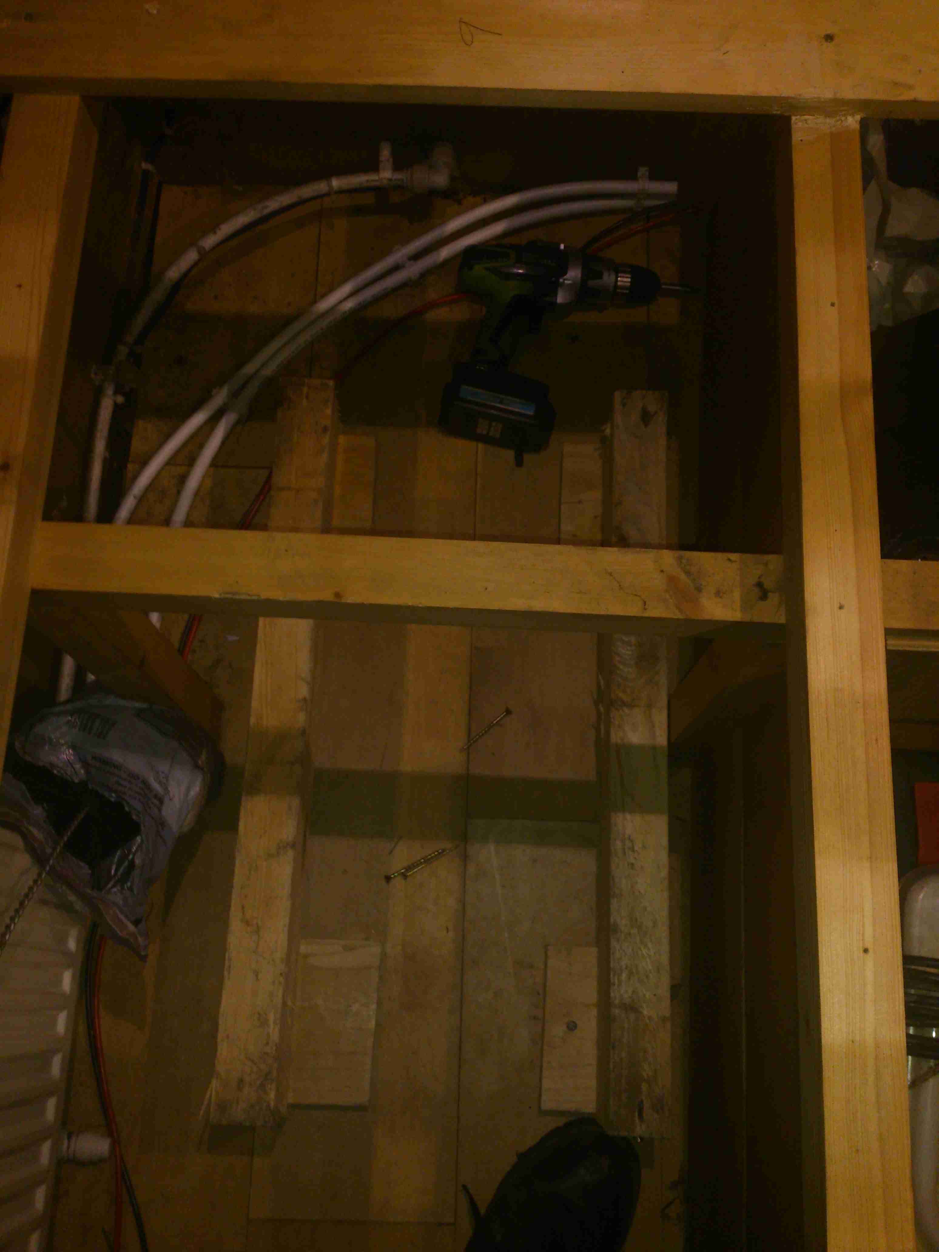
Bearers
In one of the very few free spaces available, under a bunk. A pair of timbers has been screwed to the floor to support the tank.
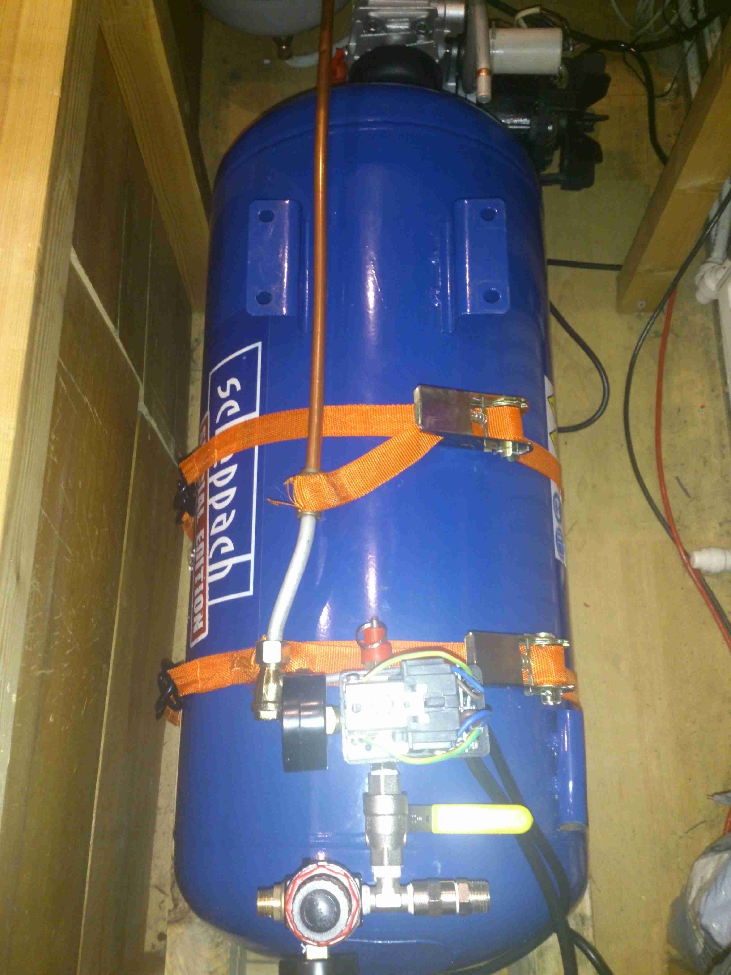
Tank Installed
The tank is strapped to the wooden supports with a pair of ratchet straps, the compressor itself can be seen just behind the tank. The copper line on the top of the tank is going back to be connected to the compressor outlet.
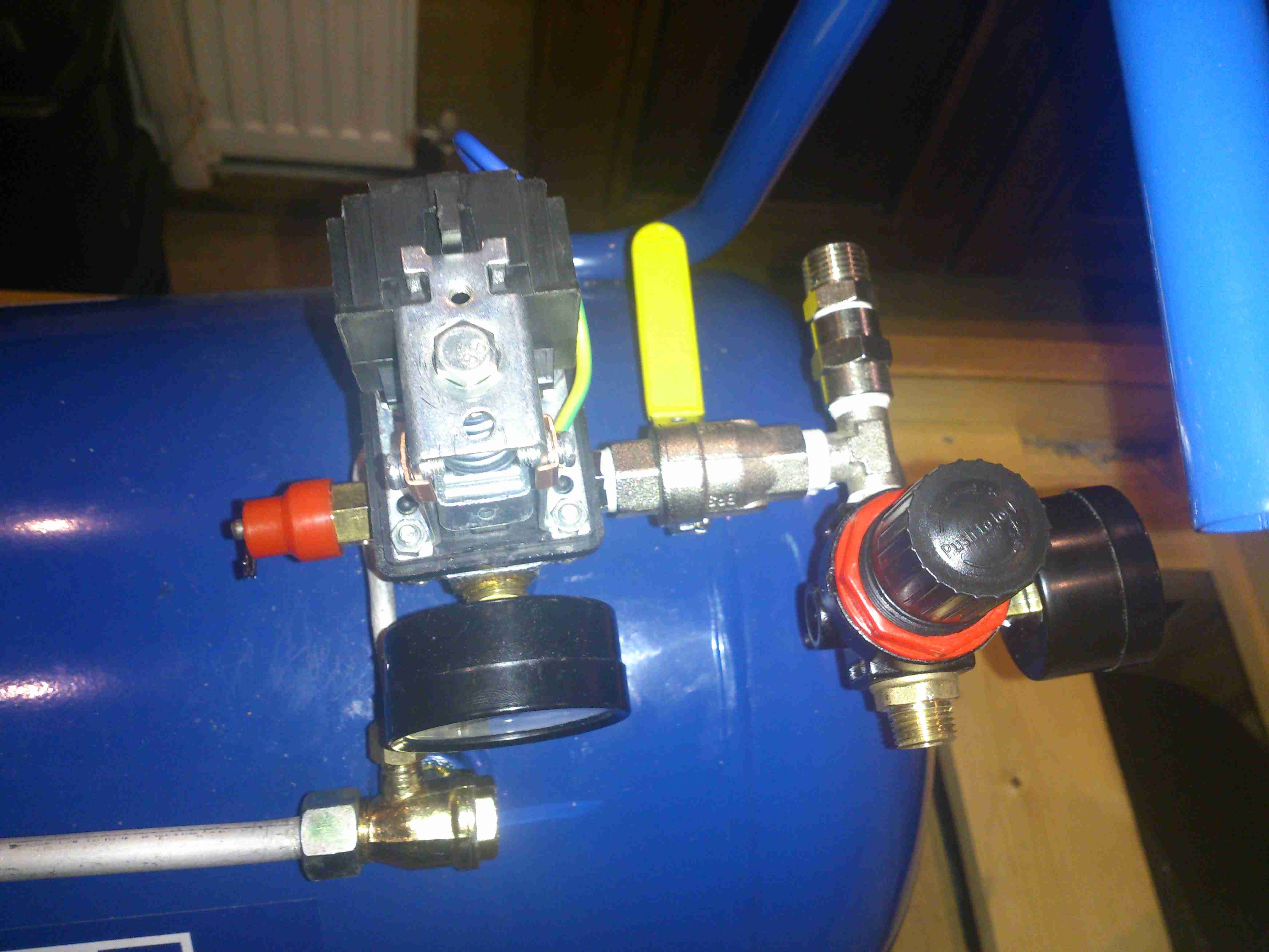
Air Fittings
Compressor control remains on top of the tank, the pressure switch & relief valve centre. After an isolation valve, the feed splits, the regulator installed will be feeding the air horn with 20PSI, replacing the existing automotive-style 12v air pump. The currently open fitting will be routed to a quick connect on the bulkhead. This will be accessible from the front deck, an air hose can be fitted to get a supply anywhere on board.
More to come when the rest of the system gets installed!
The multimode dimming/flashing modes on Chinese torches have irritated me for a while. If I buy a torch, it’s to illuminate something I’m doing, not to test if people around me have photosensitive epilepsy.
Looking at the PCB in the LED module of the torch, a couple of components are evident:
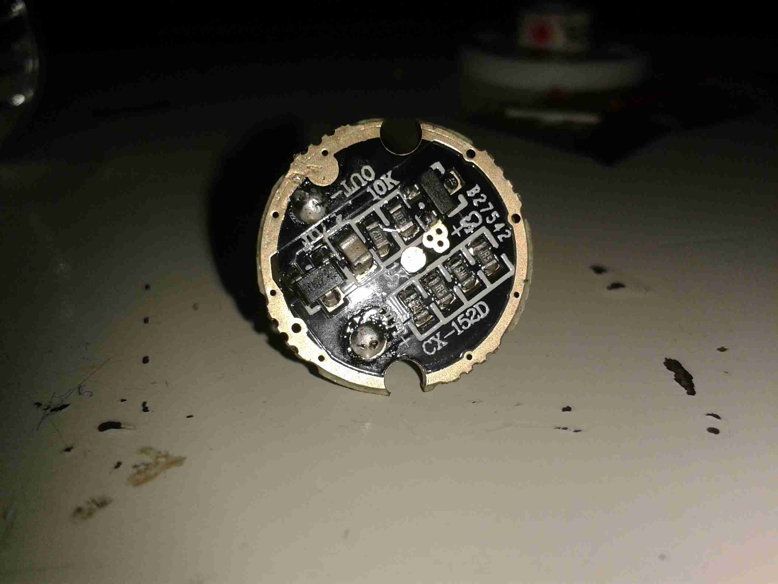
LED Driver PCB
There’s not much to this driver, it’s simply resistive for LED protection (the 4 resistors in a row at the bottom of the board).
The components at the top are the multimode circuitry. The SOT-23 IC on the left is a CX2809 LED Driver, with several modes. The SOT-23 on the right is a MOSFET, for switching the actual LED itself. I couldn’t find a datasheet for the IC itself, but I did find a schematic that seems to match up with what’s on the board.
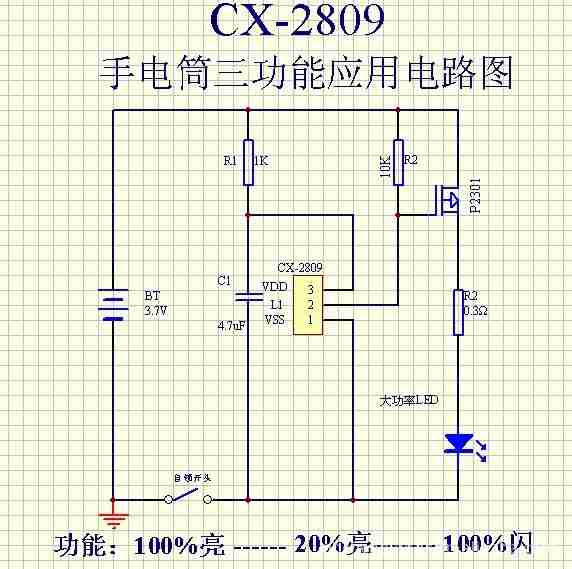
Schematic
Here’s that schematic, the only thing that needs to be done to convert the torch to single mode ON/OFF at full brightness, is to bridge out that FET.
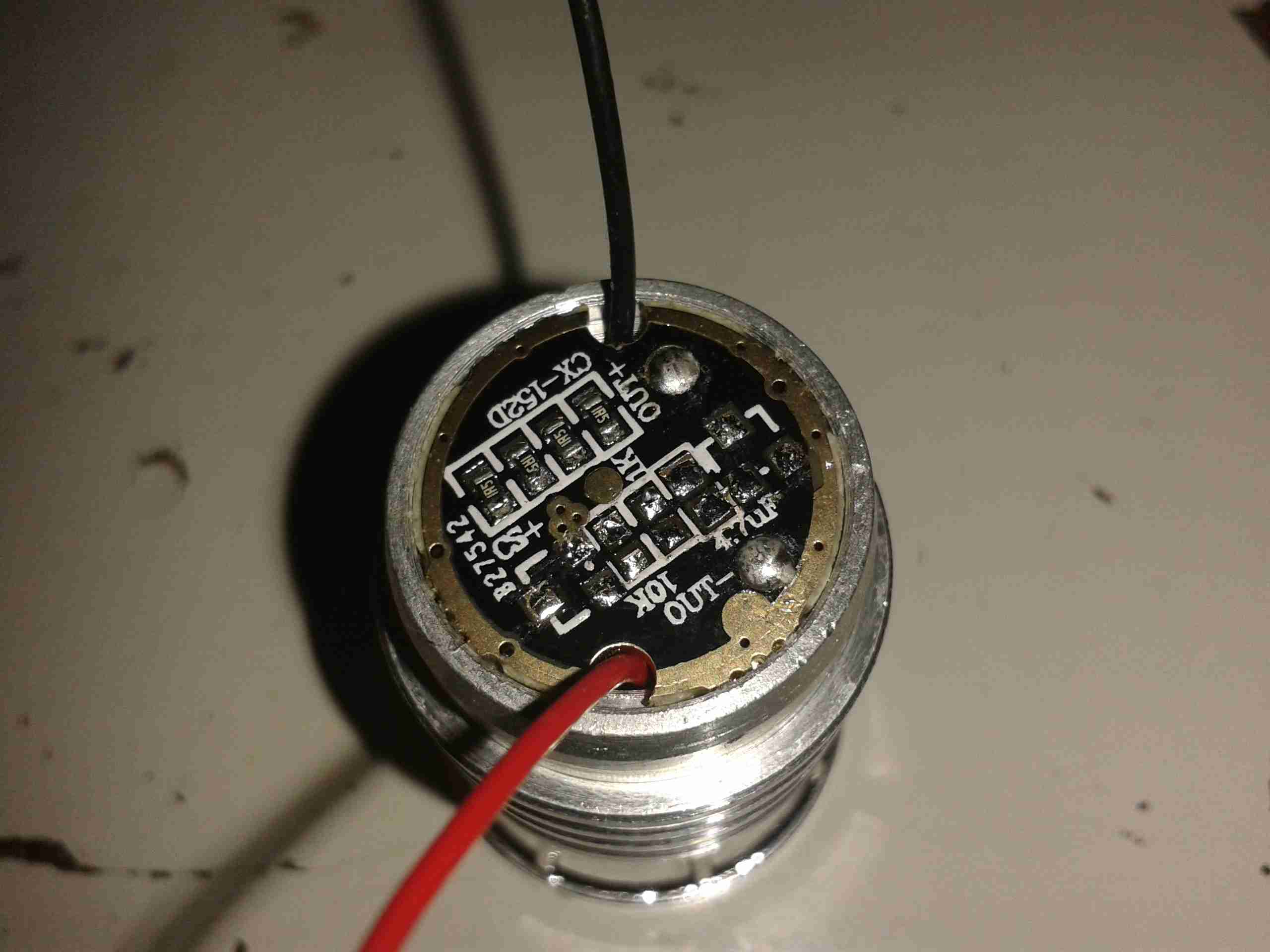
Components Desoldered
To help save the extra few mA the IC & associated circuitry will draw from the battery, I have removed all of the components involved in the multimode control. This leaves just the current limiting resistors for the LED itself.
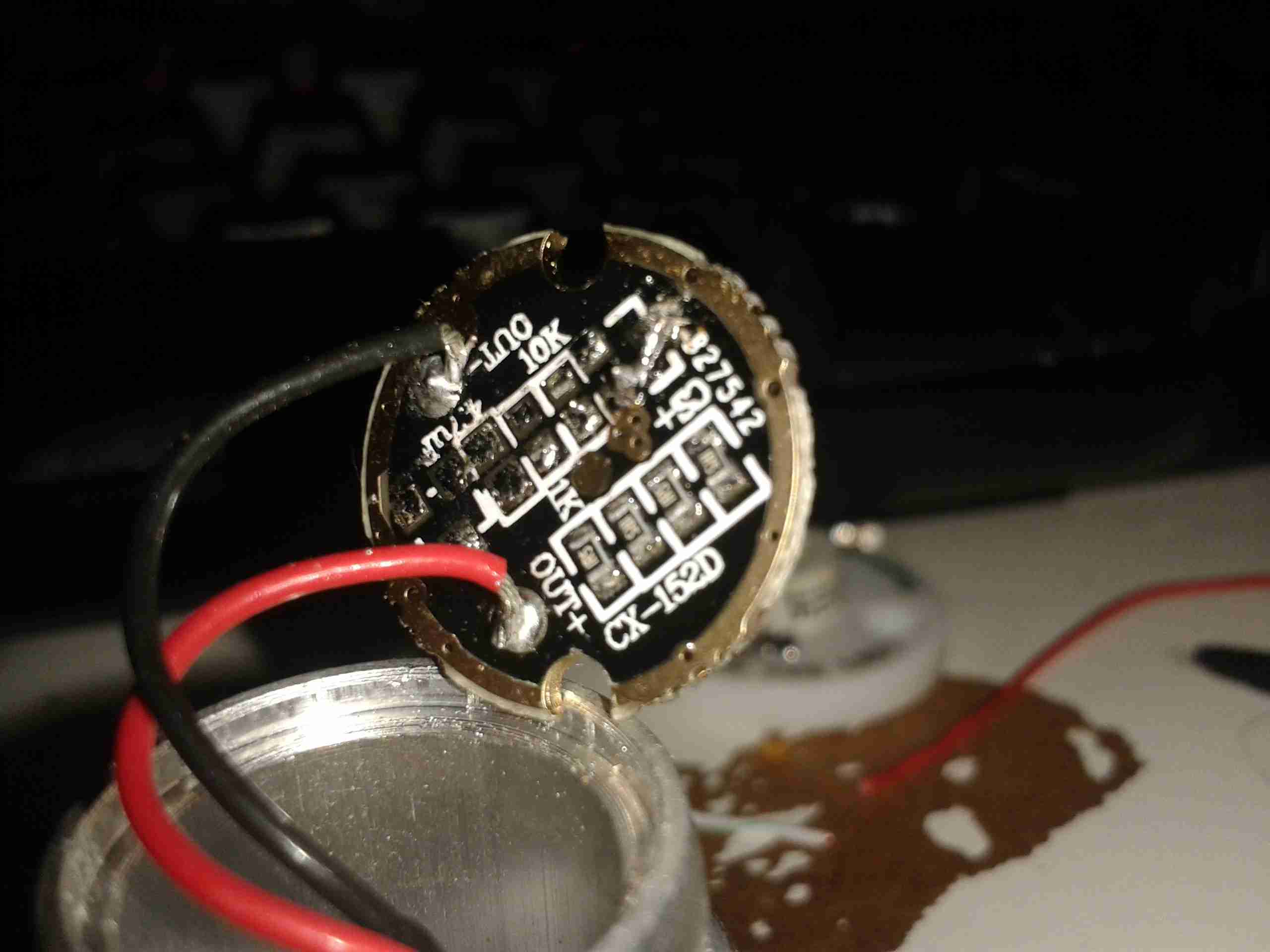
Jumper Link
The final part above, is to install a small link across the Drain & Source pads of the FET. Now the switch controls the LED directly with no silly electronics in between. A proper torch at last.
Now the controllers have arrived, I can rejig the supplies to have proper thermal control on their cooling.
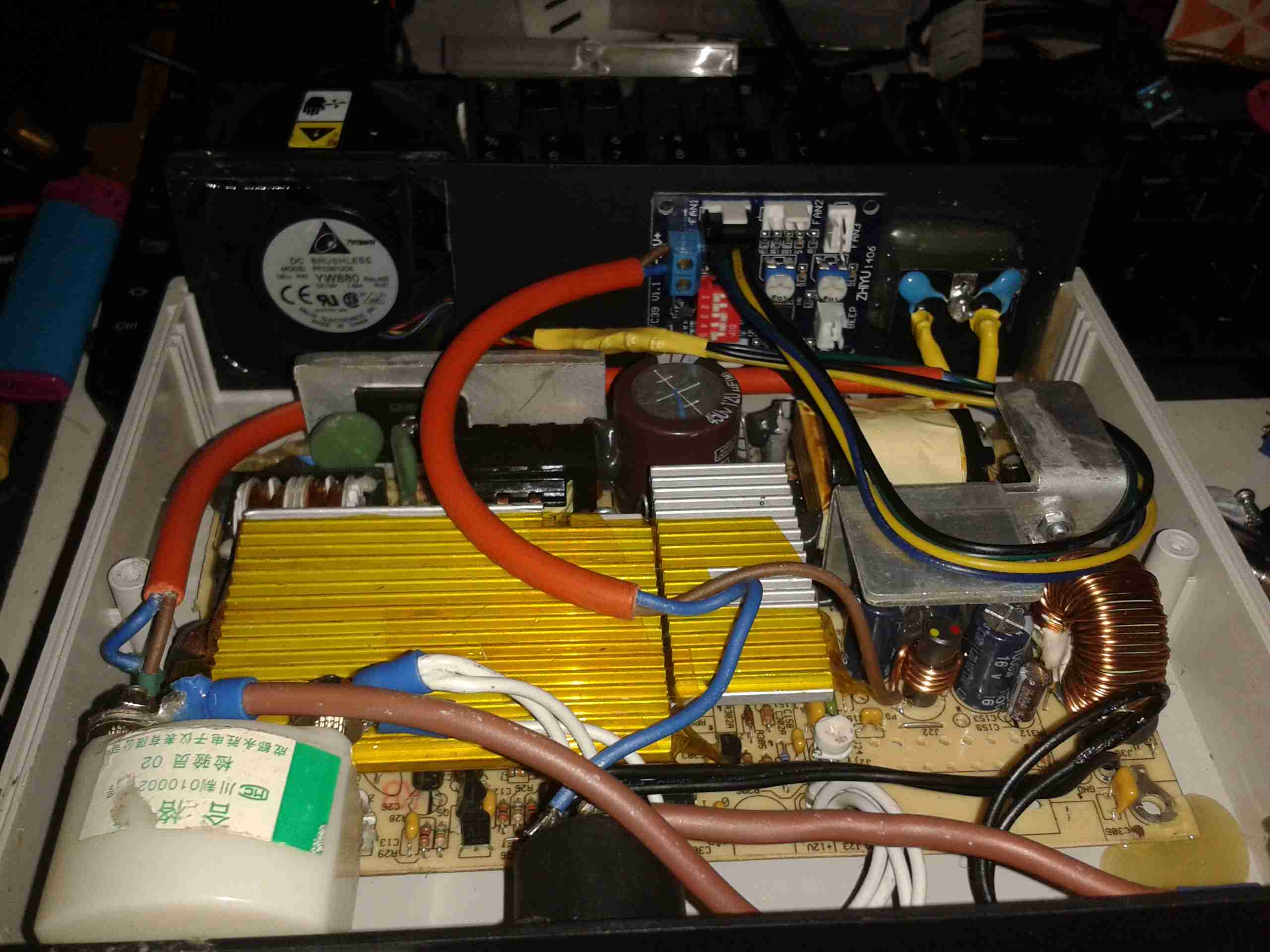
Changes Overview
Here’s the top off the PSU. The board has been added to the back panel, getting it’s 12v supply from the cable that originally fed the fan directly. Luckily there was just enough length on the temperature probe to fit it to the output rectifier heatsink without modification.
To connect to the standard 4-pin headers on the controller, I’ve spliced on a PC fan extension cable, as these fans spent their previous lives in servers, with odd custom connectors.
Fan Controller
Here’s the controller itself, the temperature probe is inserted between the main transformer & the rectifier heatsink.
I’ve set the controller to start accelerating the fan at 50°C, with full speed at 70°C.
Full Load Test
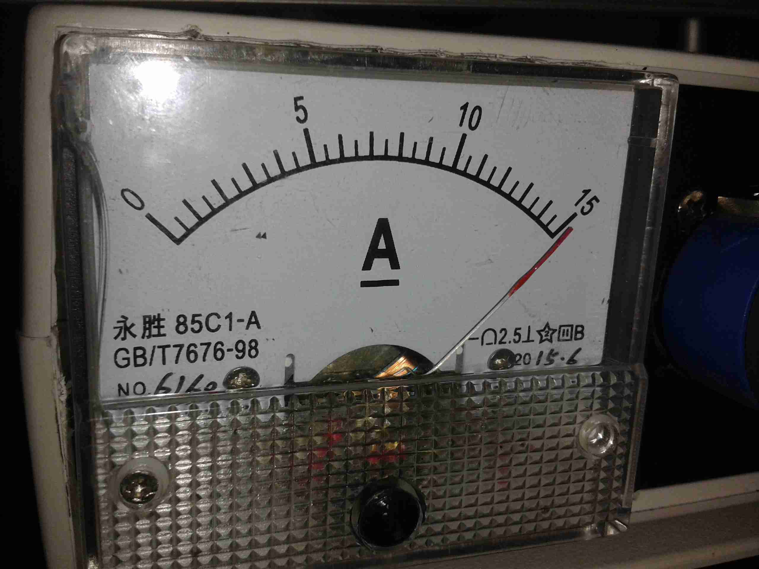
Under a full load test for 1 hour, the fan didn’t even speed up past about 40% of full power. The very high airflow from these fans is doing an excellent job of keeping the supply cool. Previously the entire case was very hot to the touch, now everything is cool & just a hint of warm air exits the vents. As the fan never runs at full speed, the noise isn’t too deafening, and immediately spools back down to minimum power when the load is removed.
While I’m waiting for the fan controllers to arrive for the new cooling fans, I figured I’d get them fitted into the cases of the supplies & just have them run at minimum speed for now.
Fan Fitted
After removing the original small fan, I cut a larger square hole in the panel to fit the 60mm version. These fans only fit with some minor adjustment to the top & bottom mouldings, but the look isn’t too bad once the covers are back on. The wiring is routed through a small hole next to the fan itself.
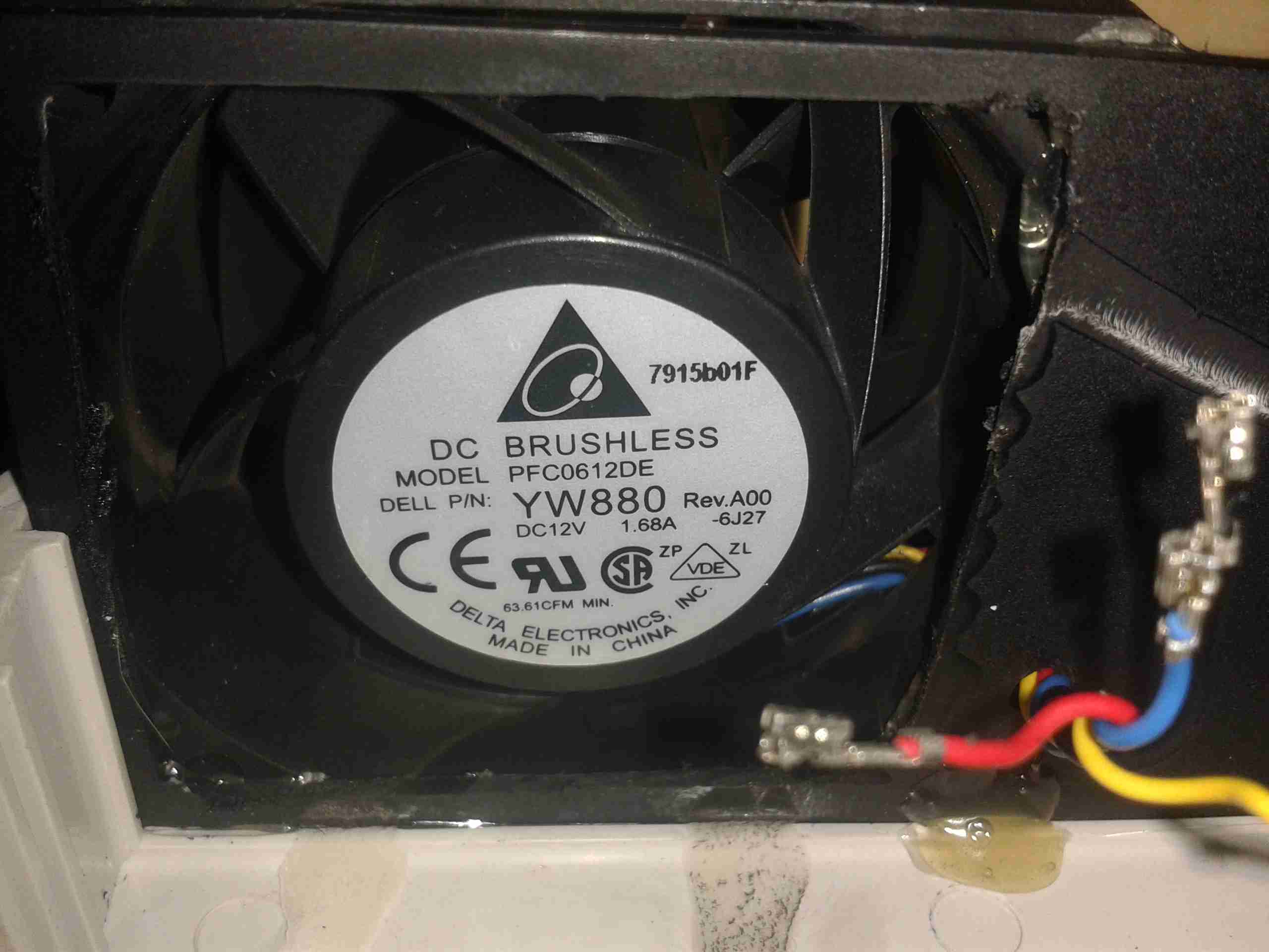
I’ve also upgraded on the fans again – these are PFC0612DE, with a higher airflow of ~70CFM at 12,000RPM.
To get the fans to run at minimum speed, the PWM control wire is connected directly to GND.
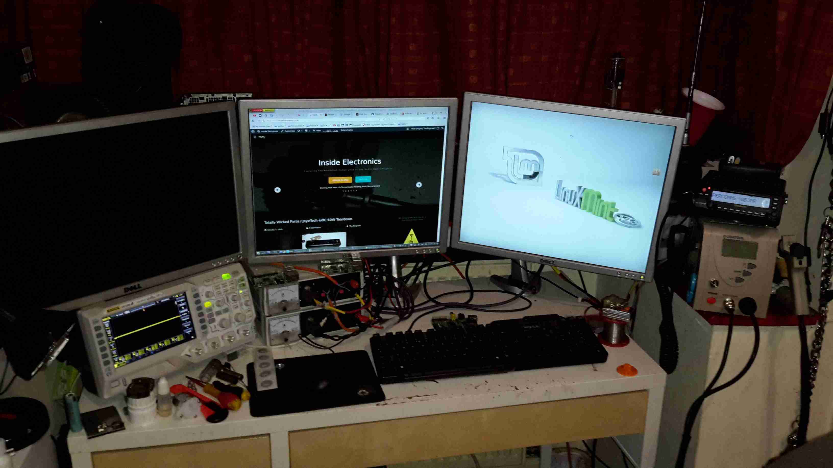
Main radio of course is housed on the left, it’s partially hidden under my currently over-populated breadboard.
All 3 monitors are linked to the same PC, using a pair of video cards. This is a very flexible system with so much screen real estate.
Main system power is provided by the pair of power supplies next to the radio – these are homebrew units using surplus switched mode PSU boards. Check my previous posts for more details.
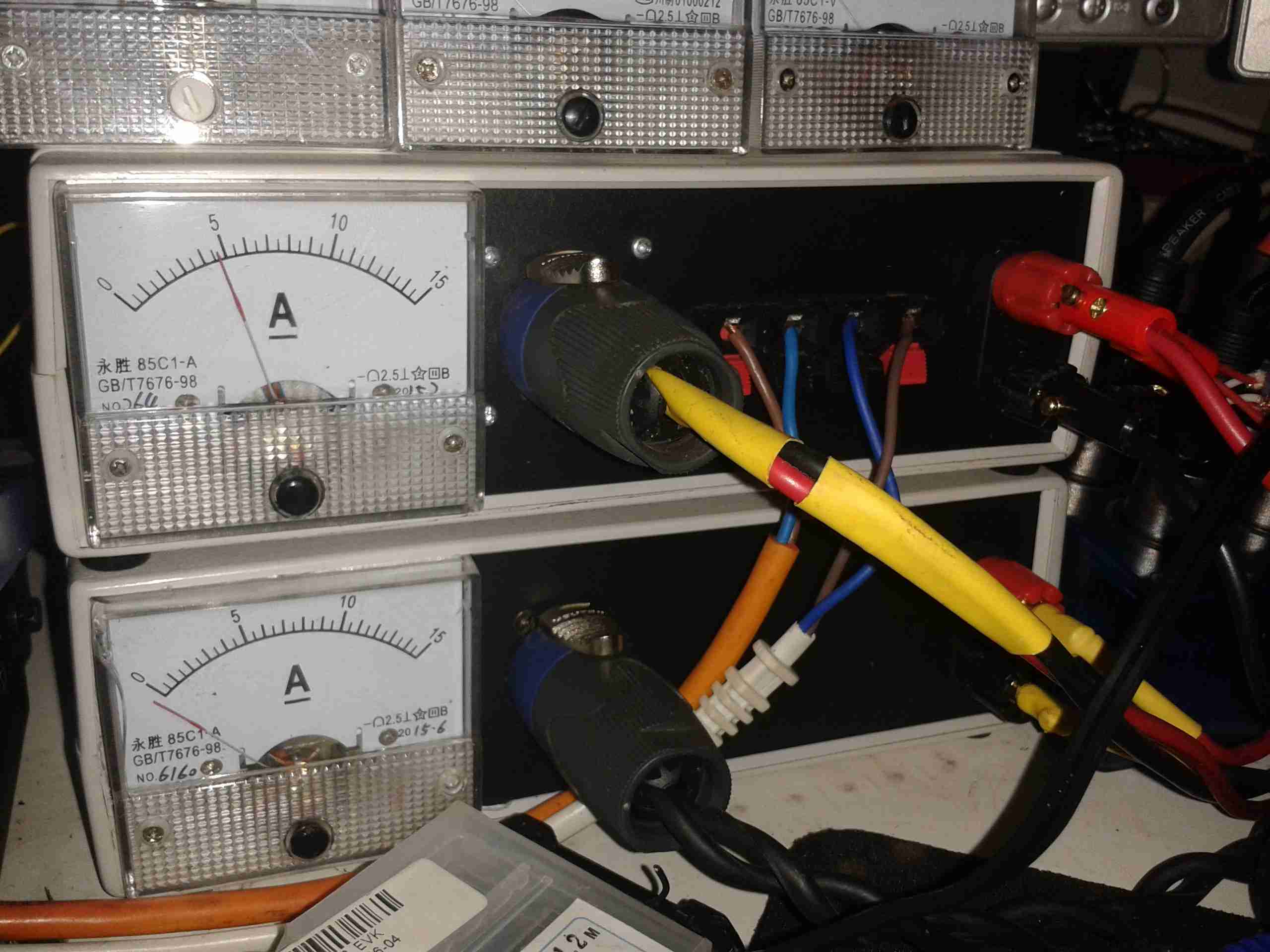
Power Supplies
The mainpowersupply system. These two supplies are cross connected, giving a total DC amperage of 30A at 13.8v. There is also a link to a large 220Ah lead-acid battery bank (orange cable), to keep me on the air during power outages. This cable is getting upgraded to something more beefy shortly. The white cable is currently supplying power to my onlineradiation monitor.
The main high-currentDC outputs are the Speakon connectors next to the meters. The top one is powering the radio directly, the bottom is linked through to my 12v distribution box for lower current loads, such as the oscilloscope, audio amplifiers, tools, etc.
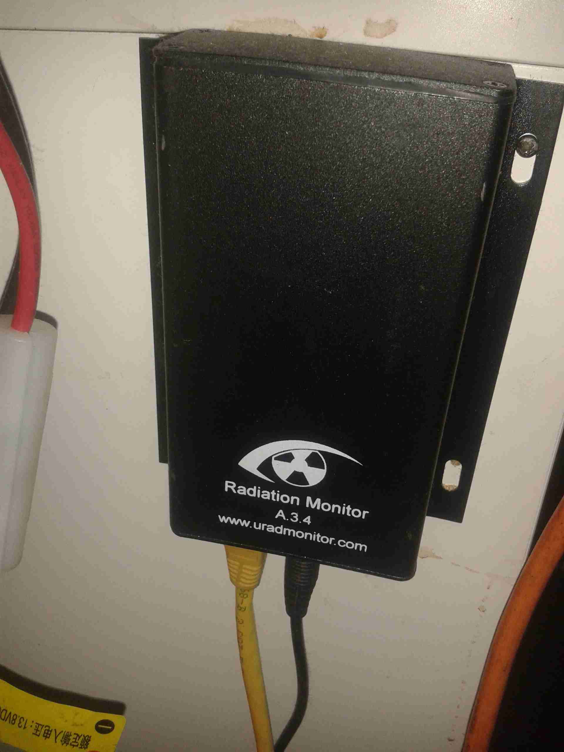
Radiation Monitor
Attached to the side of the desk is the radiation monitor itself.
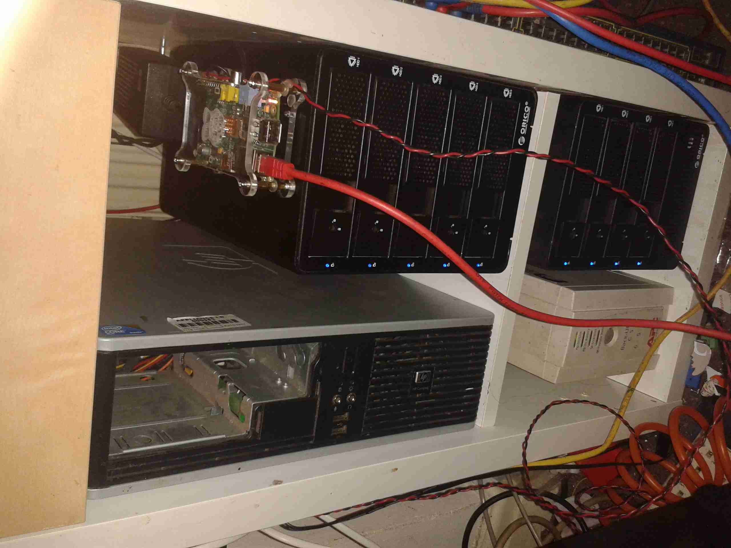
Core NAS
Under the radio is the core NAS of the network. It’s an array of 9 4TB disks, in RAID6, giving a total capacity after parity of 28TB. This provides storage & services to every other machine in the shack, the Raspberry Pi on top of the disk array is doing general network housekeeping & monitoring, also generating the graphs for the Radiation Monitor page. A Cisco 48-portswitch is partially out of frame on the right, providing 100MB Ethernet to the devices that don’t require gigabit.
I’m still on my crusade of removing every trace of 240v mains power from my shack, so next up are my computer monitors.
I have 4 Dell monitors, of various models, hooked up to my main PC.
The monitor here is a Dell E207WFPc 20″ widescreen model. There will be more when I manage to get the others apart to do the conversion. However I’m hoping that the PSU boards are mostly the same.
Panel Removed
There are no screws holding these monitors together, the front bezel is simply clicked into place in the back casing, these clips are the only thing that holds the relatively heavy glass LCD panel & it’s supporting frame! The image above shows the panel removed. The large board on the left is the power supply & backlight inverter, the smaller one on the right is the interface board to convert the DVI or VGA to LVDS for the LCD panel itself.
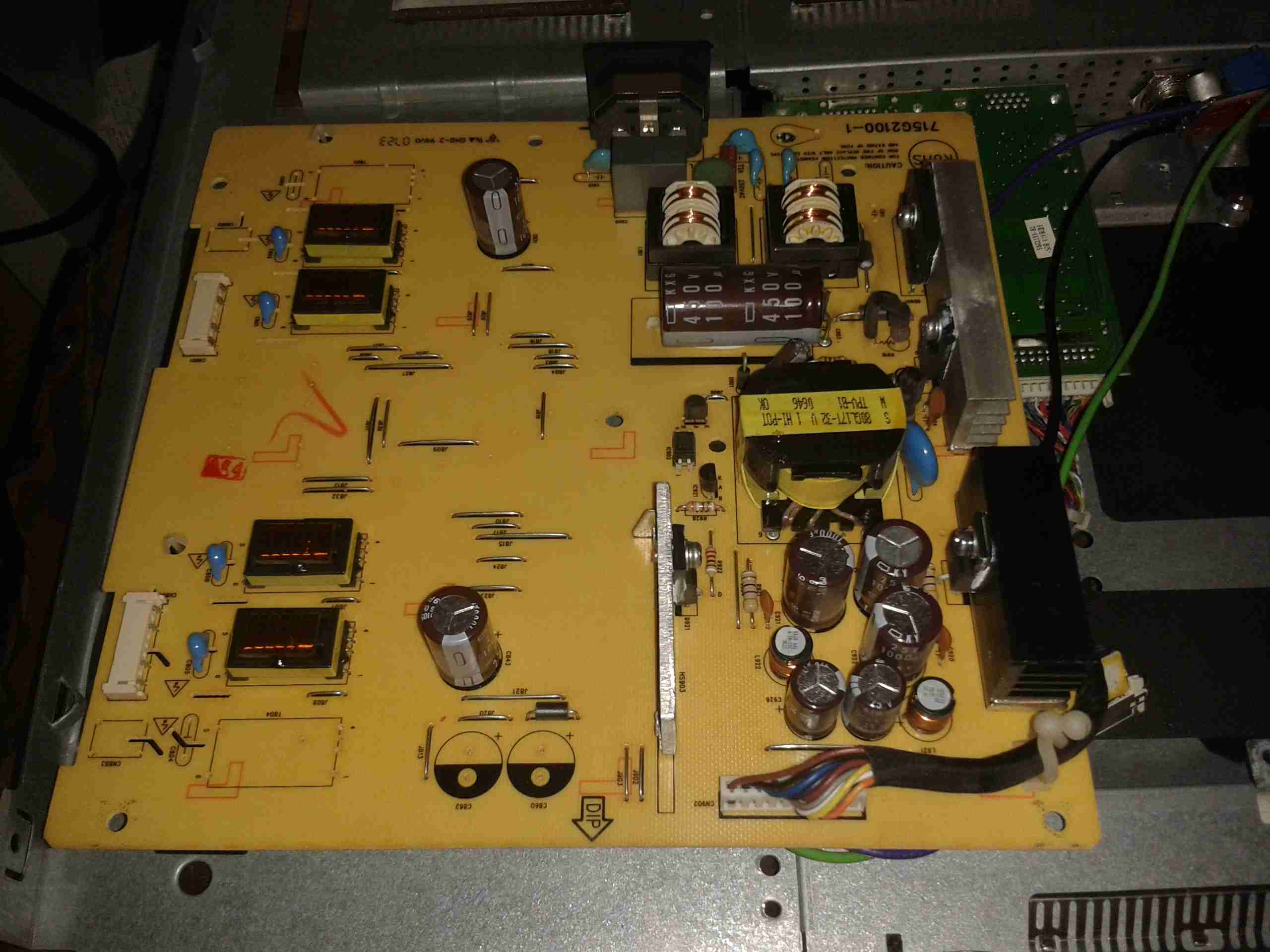
PSU Board
Here’s a closeup of the PSU board, the connector at centre right at the top of the PCB is the main power output, and also has a couple of signals to control the backlight inverter section of the PSU, on the left side. The PSU requirements for this monitor are relatively simple, at 14.5v for the backlight & 5v for the logic board.
PSU
Here’s the top of the PSU board, very simple with the mains supply on the right side, and the backlight inverter transformers on the left.
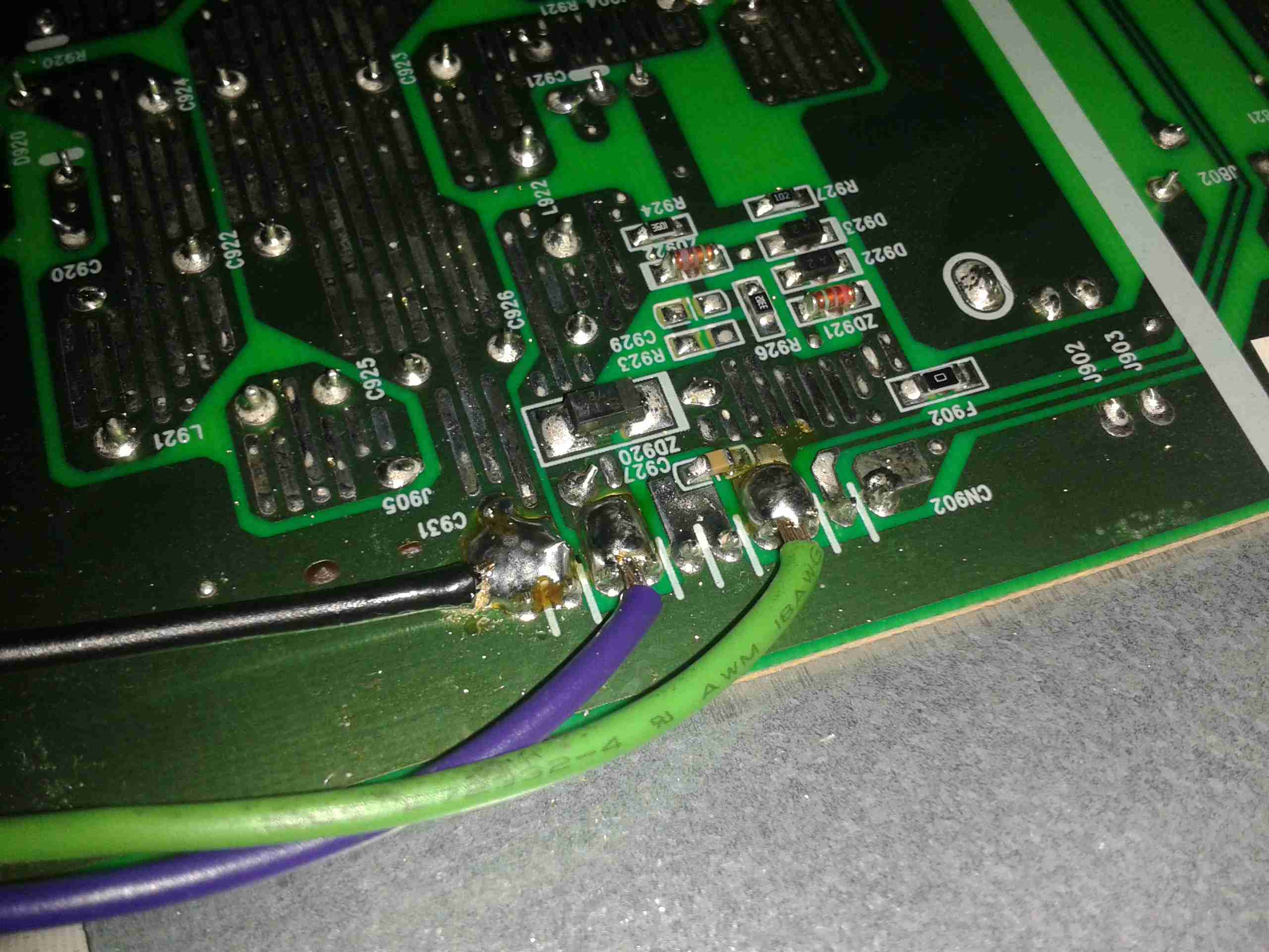
Hooked In
Here I’ve hooked into the power rails on the supply, to attach my own 12v regulators. The green wire is +14.5v, and the purple is +5v. Black is common ground.
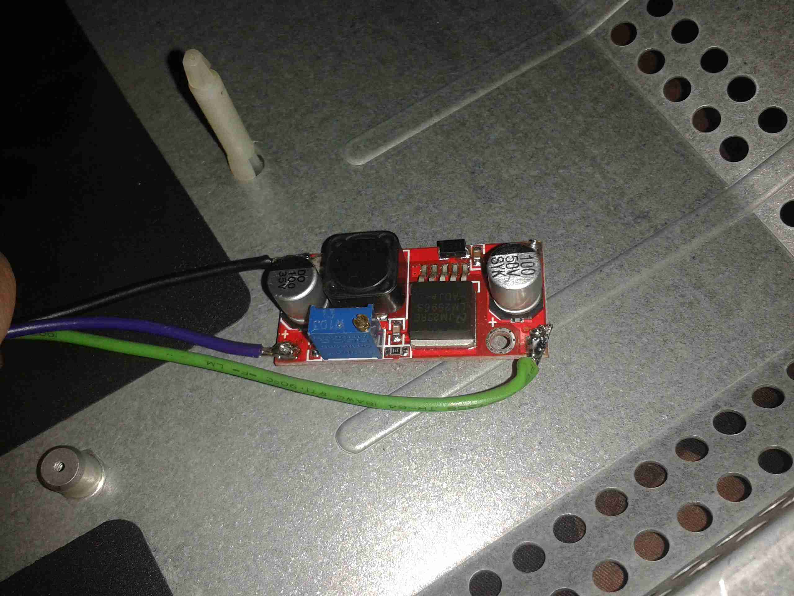
5v Regulator
On doing some testing, the backlight inverter section doesn’t seem to mind voltages between 11.5-14.5v, so a separate regulator isn’t required there. Even running off batteries that’s within the range of both charging & discharging. The only regulator required is a 5v one to reduce the input voltage for the logic PCB.
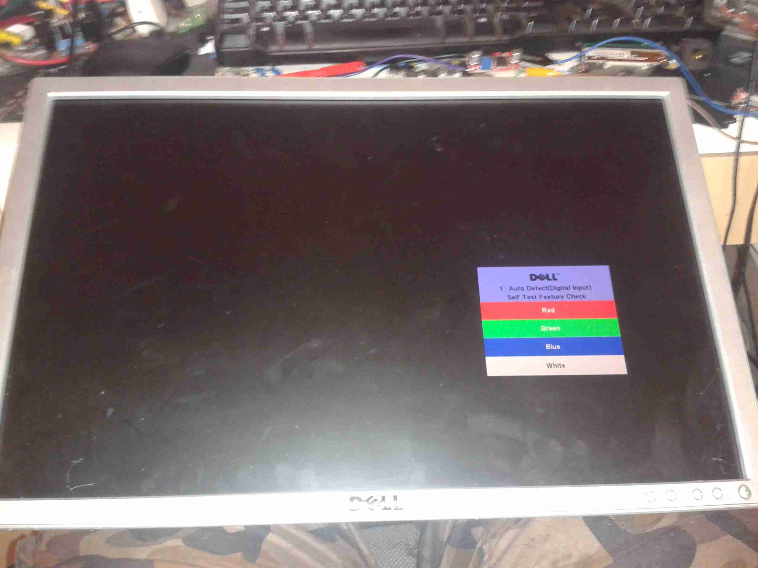
First Test
On applying some 12v power to the regulator input, we have light! Current draw at 12.5v is 2.65A for a power consumption of 33W.
12v Input
There’s plenty of room in the back casing to mount a 12v input socket, I have left the mains supply intact so it can be used on dual supply.
Final Wiring
Here’s the 5v regulator mounted on the back of the casing, all wired up & ready to go.
I’ve had a couple of larger batteries for my UV-5Rs for some time now, and decided to do a quick teardown to see if they’re actually the capacity claimed.
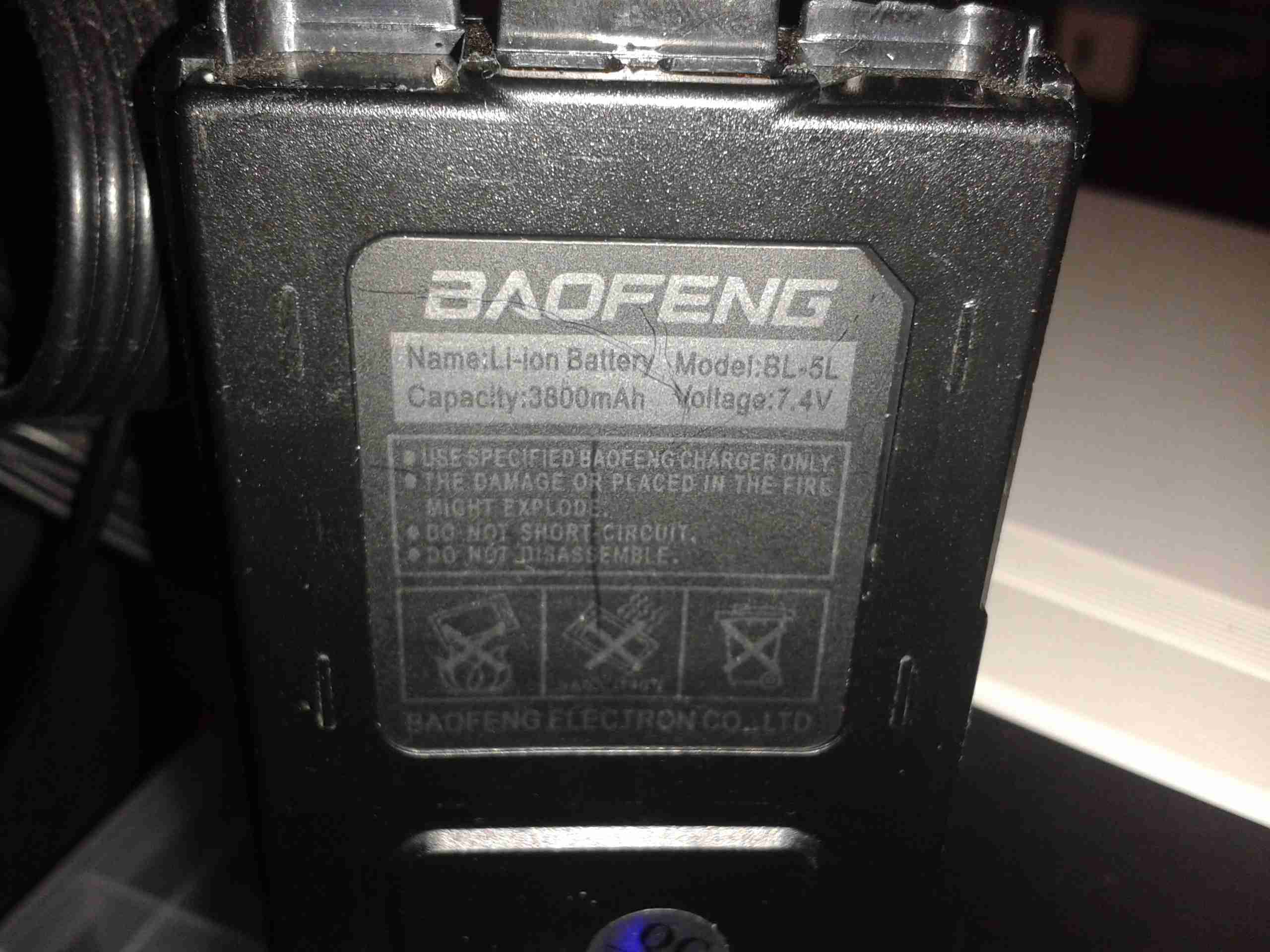
BL-5L Battery
Here’s the label, claiming 3800mAh (3.8Ah) of battery capacity.
These batteries are held together with glue, but a good way to get these kinds of things open is by whacking the seams with the handle of a screwdriver. This cracks the glue without damaging the casing.
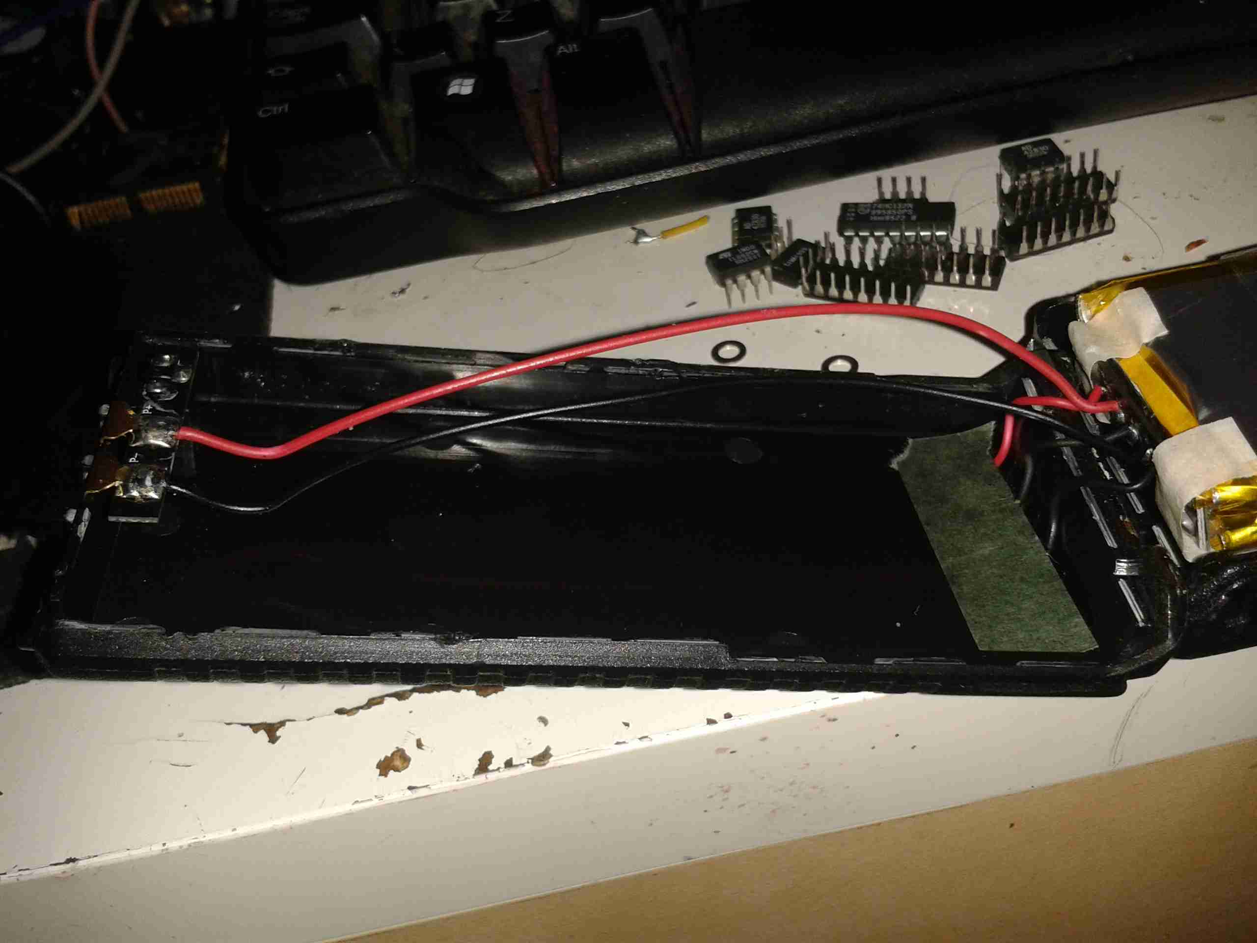
Battery Cracked Open
After a few minutes of cracking the seams, the battery comes right open. The pair of wires link the protection board on the cells to the DC terminals on the top of the pack. The charging terminals are under the cardboard insulator on the right.
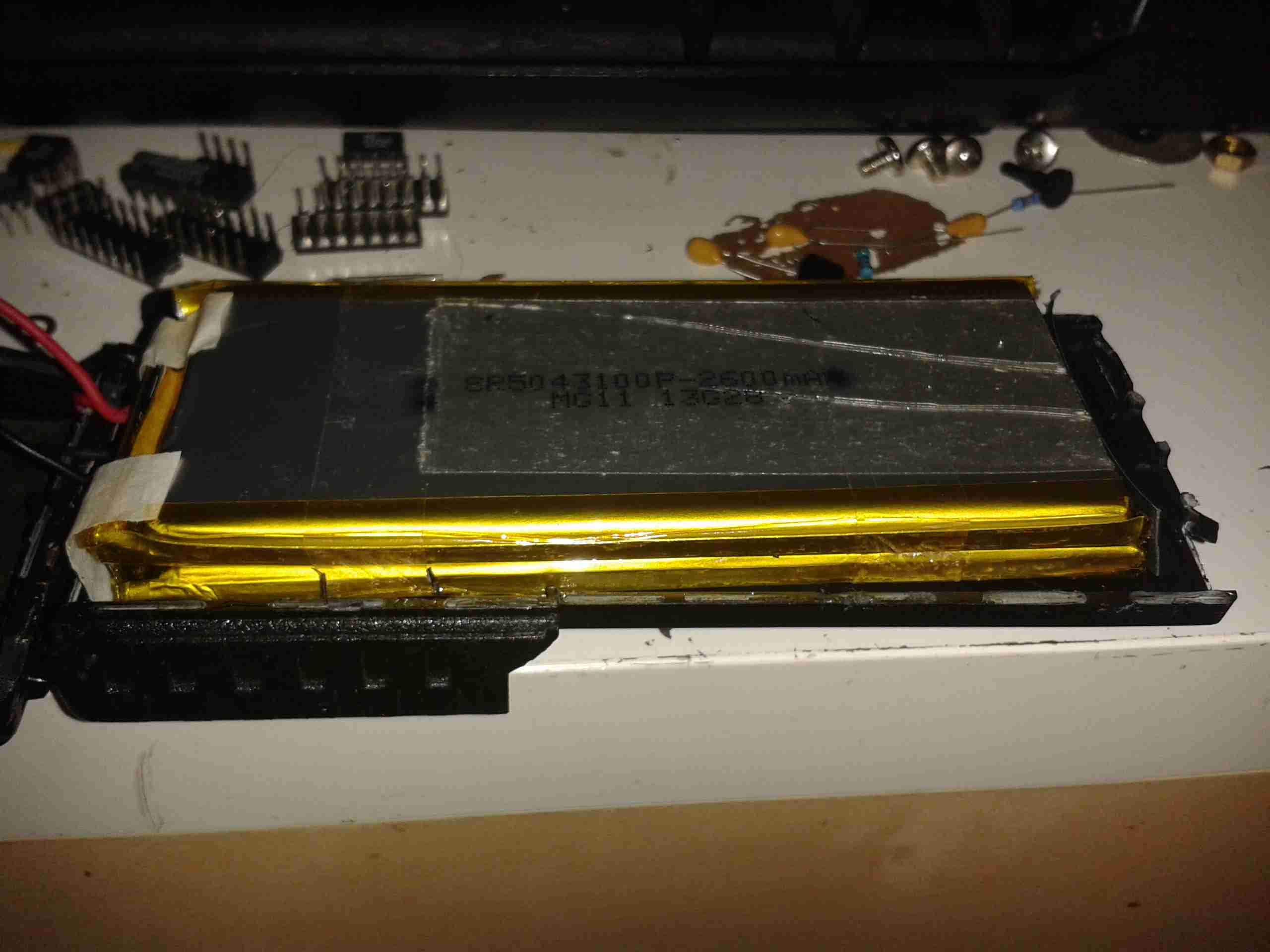
Cells
Here’s the other half of the case, with the cells themselves. These are wired in series for a 7.2v pack, and at a capacity of 2600mAh (2.6Ah) printed on them, the label clearly lies about the capacity.
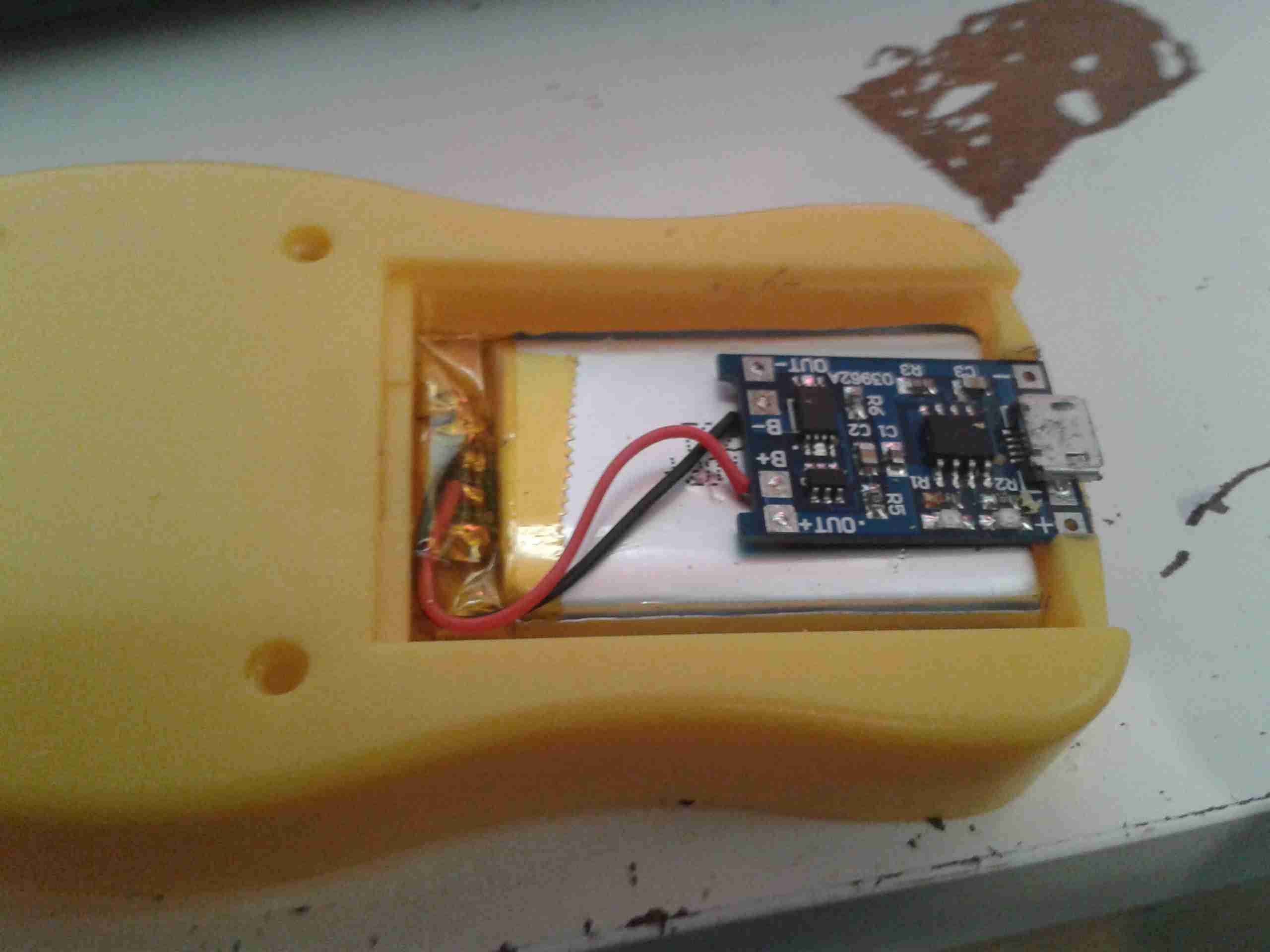
From the factory, the GY561 meter uses alkaline AAA cells for power. As these are not rechargable, and I don’t carry any other devices that take such batteries, I figured I’d replace them with a single Lithium Polymer cell that I can charge via USB.
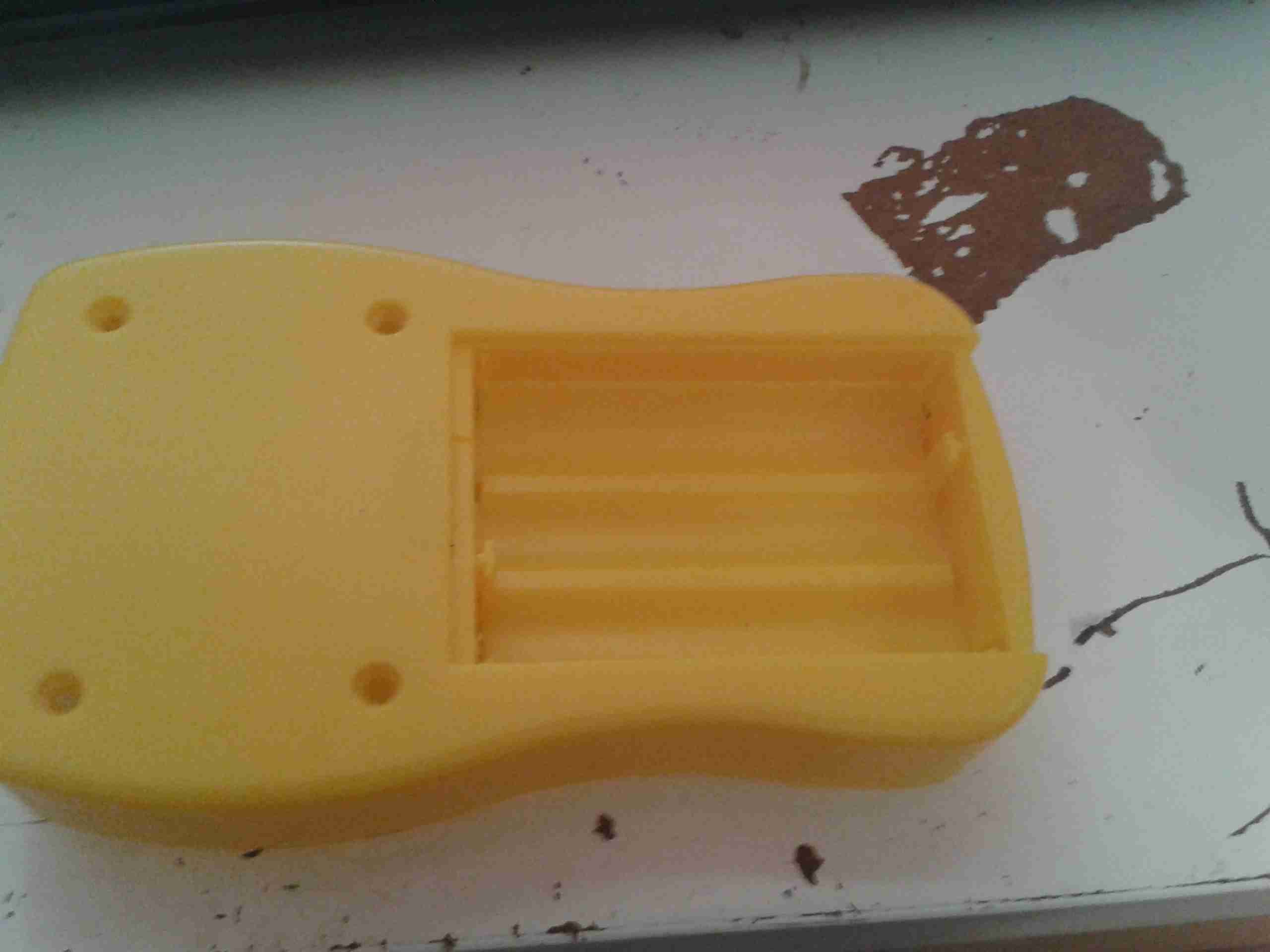
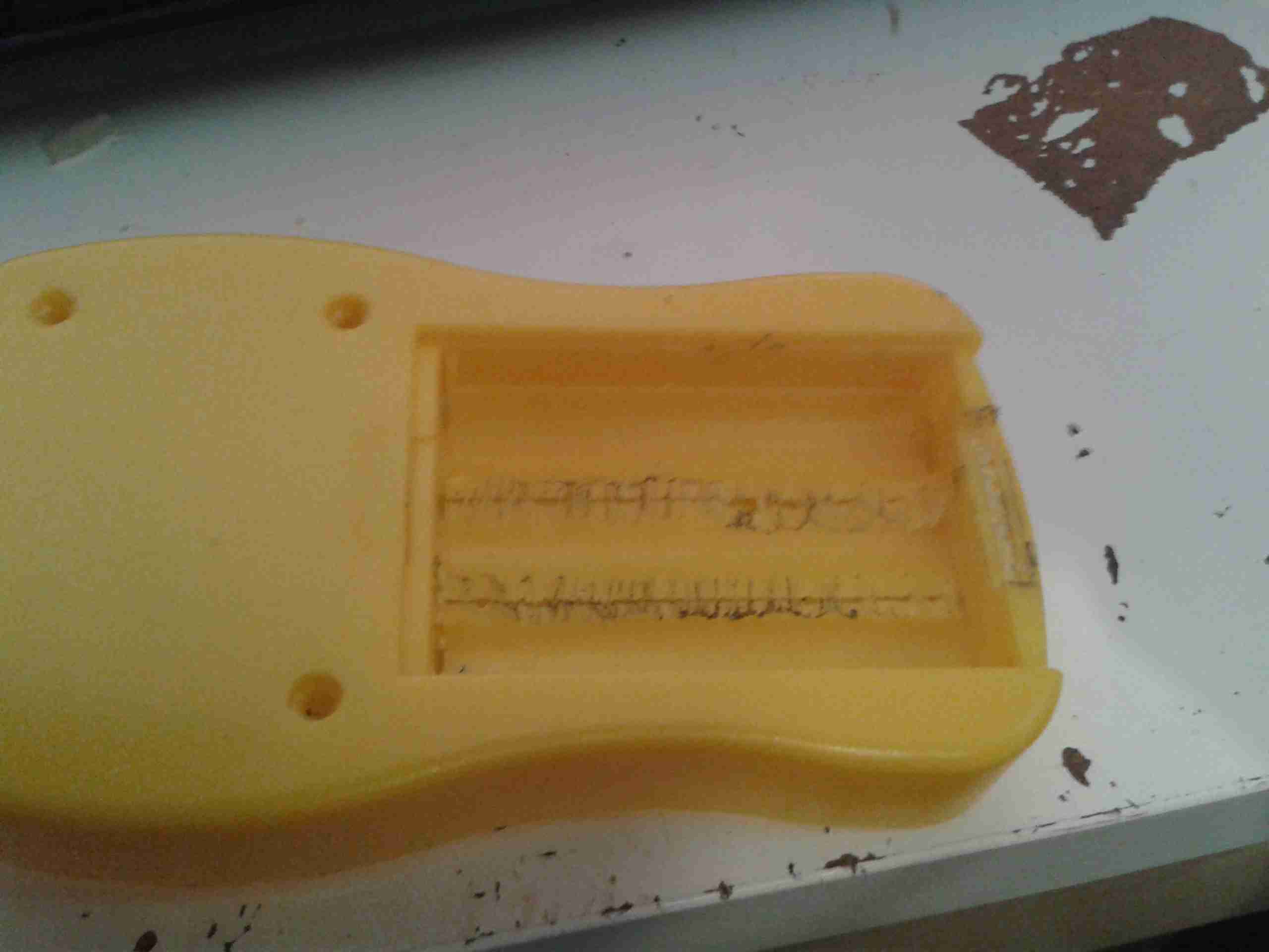
Battery Compartment
Here’s the battery compartment, with the original spring terminals removed.
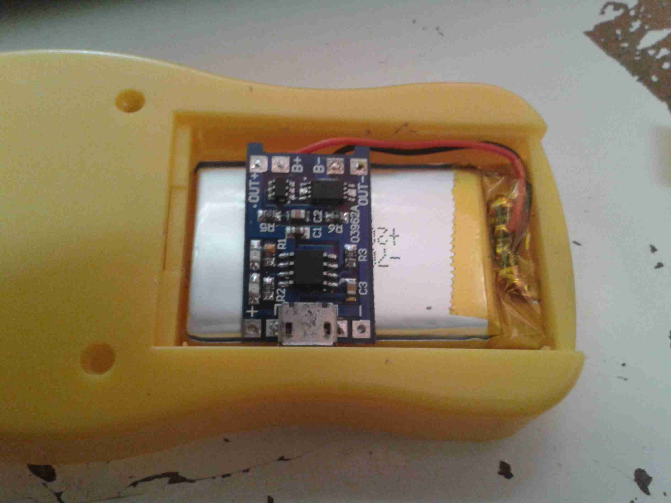
I searched eBay for a suitable sized cell, and settled on a 1000mAh type, with dimensions of 47mm x 28mm x 7mm.
This size cell required a small amount of modification to the battery compartment to make it fit properly with the associated charge & protection circuitry.
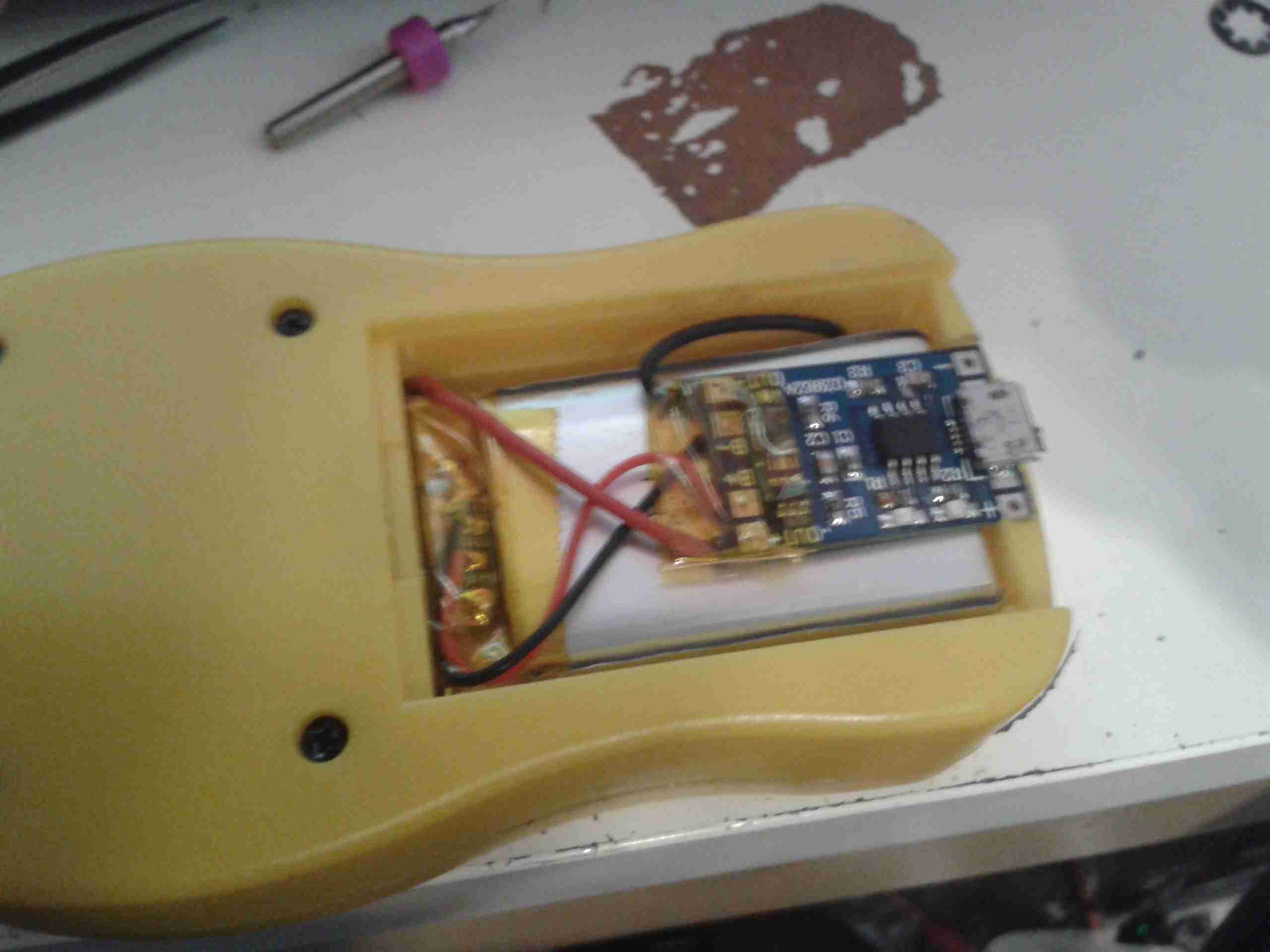
Modified Compartment
Here’s the modifications made to the compartment, I’ve ground away the plastic to make the bottom flat, and the plastic tabs that retained the original spring terminals.
Modifications
After grinding away the original battery spring holders with a dremel, the cell fits perfectly in the available space. The small PCB on the top of the cell is the USB charger & protection.
Charger
The charger is located in a slot cut in the bottom of the casing, so the USB port is accessible from outside the compartment.
Wiring
Here’s the rest of the wiring completed, with the power wires going through holes in the bottom of the battery compartment to join onto the PCB where the original terminals were located. I have insulated the solder joints on the control PCB with some Kapton tape to prevent any shorts against the lithium cell.
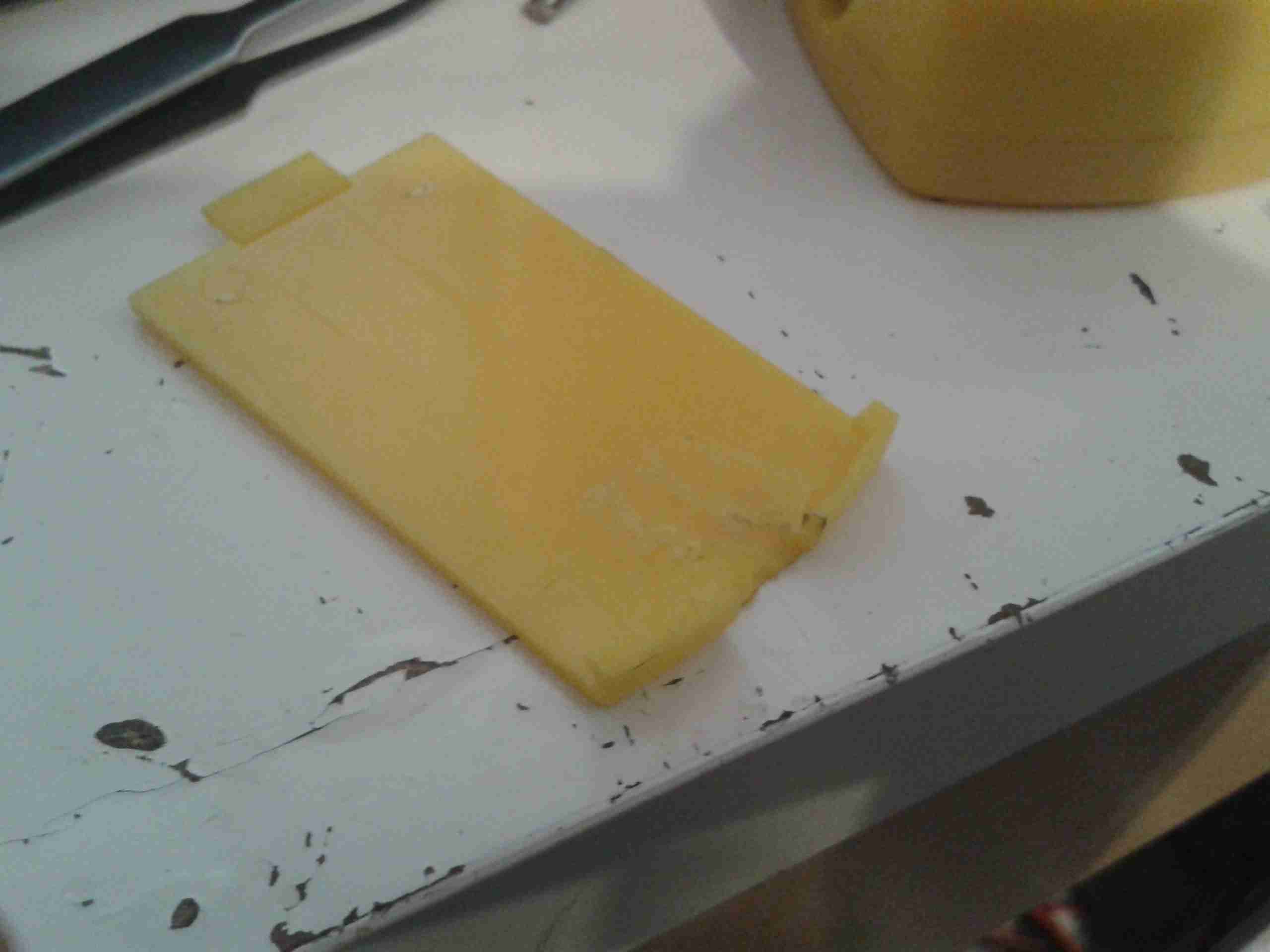
Battery Cover
A small cutout was also required in the battery cover to allow the USB connector to poke out. This was easy to do on the soft plastic with a Dremel tool.
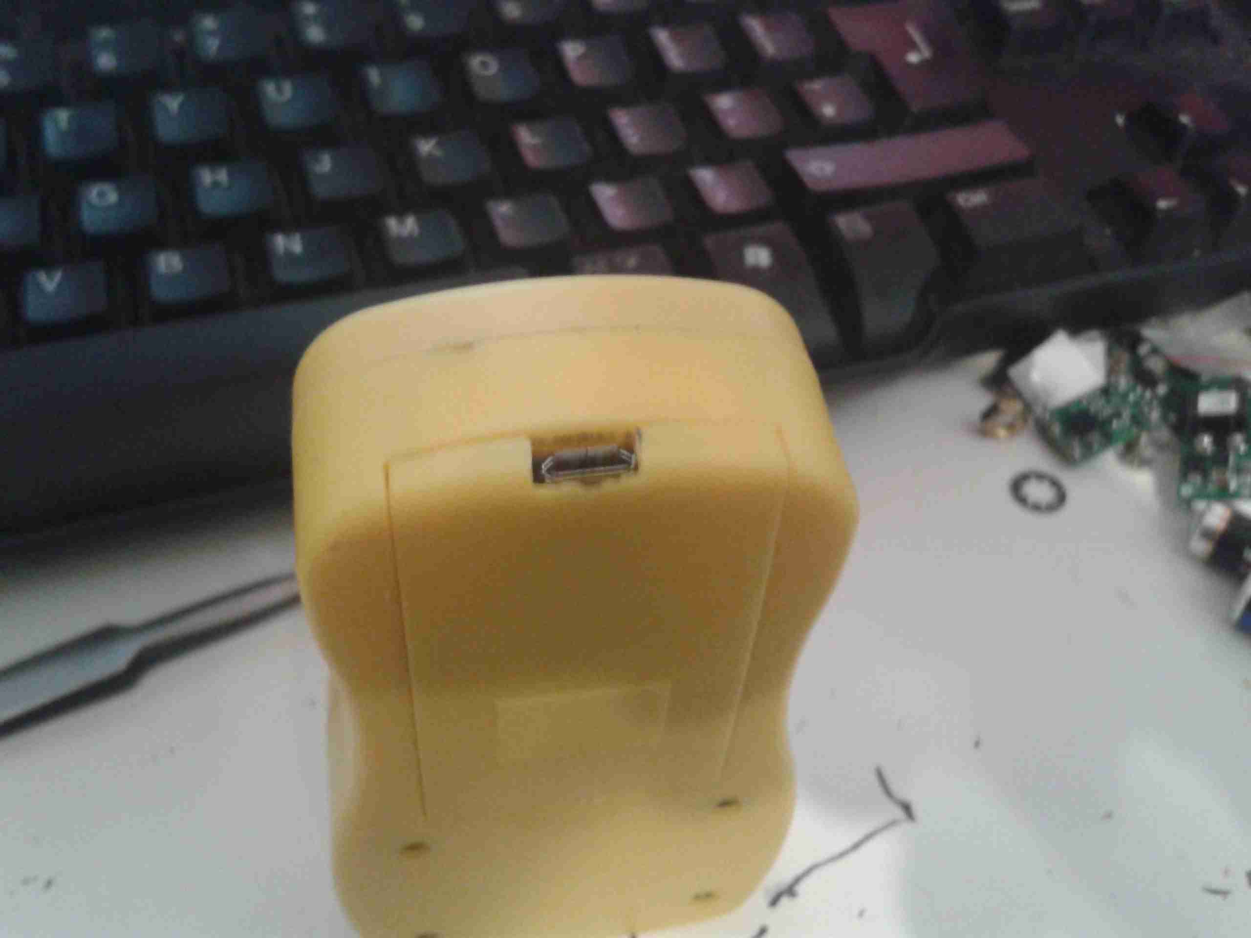
Charging Port
With the battery cover installed, the USB port is nicely recessed into the edge.
Charging LED
The indicator LEDs on the charging & control board show nicely through the plastic, here’s the unit on charge. When the charge is complete, another LED lights as shown below.
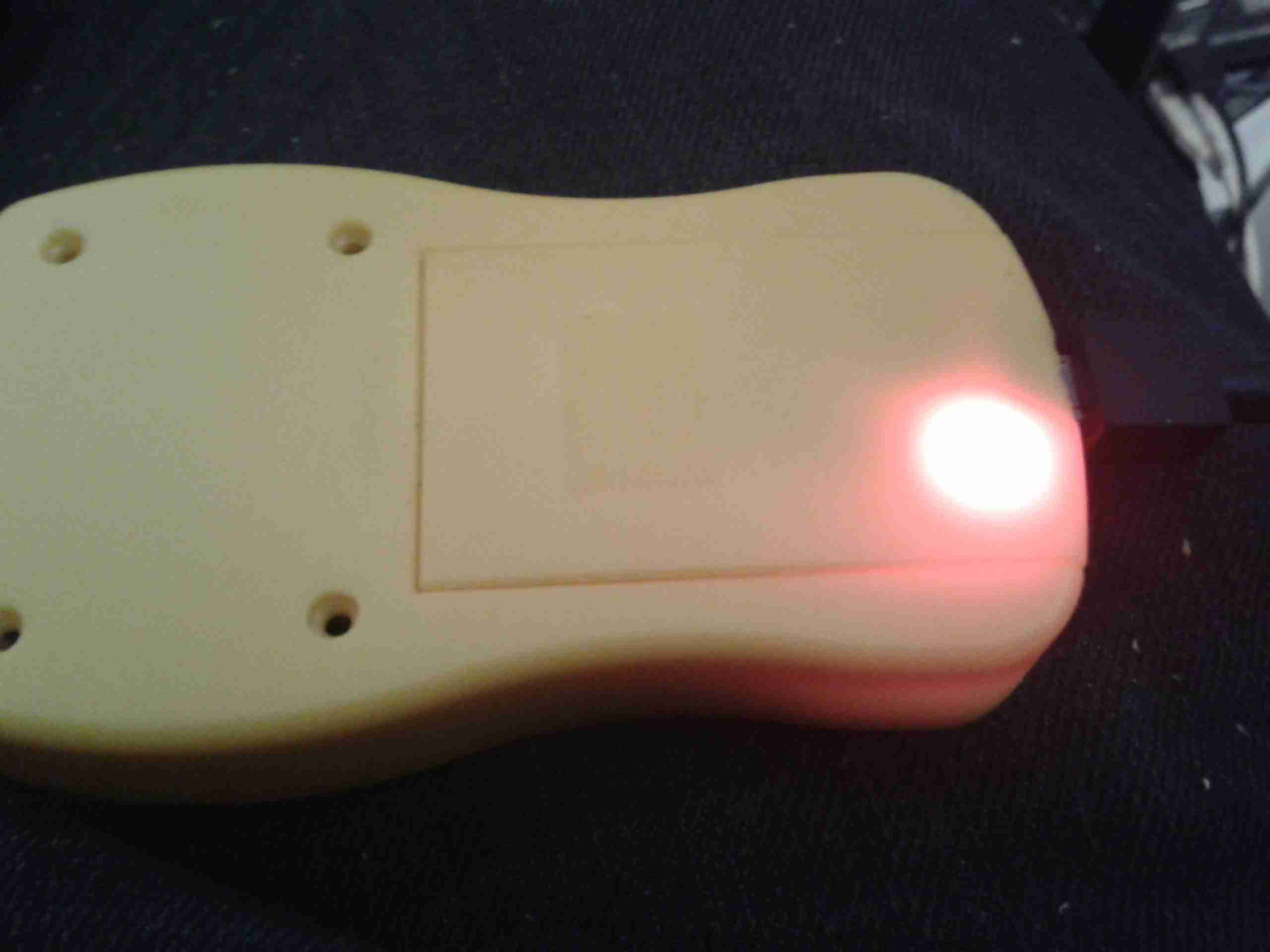
Here’s an odd & sudden failure, the power adaptor for a Samsung device. It’s been working for months & on being plugged into the mains today the magic blue smoke escaped.
Samsung Charger
It’s one of their 2A models, for charging bigger devices like tablets.
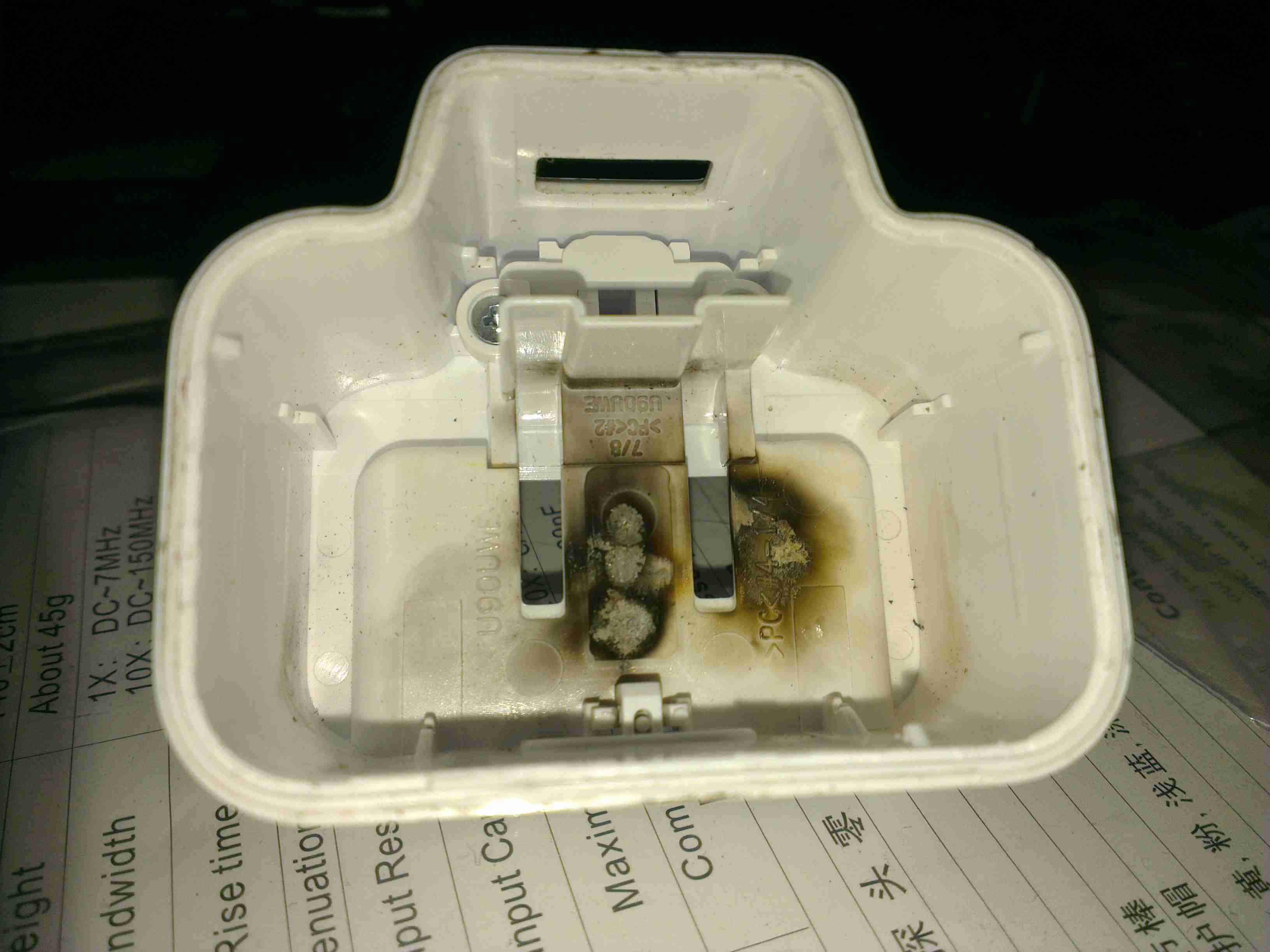
Flash Burn
Strangely for one of these chargers, no glue is used to hold it together – just clips. This made disassembly for inspection much easier. Evidence of a rather violent component failure is visible inside the back casing.
PCB
Here’s the charger PCB removed from the casing. As to be expected from Samsung, it’s a high quality unit, with all the features of a well designed SMPS.
PCB Reverse
However, on turning the board over, the blown component is easily visible. It’s the main SMPS controller IC, with a massive hole blown in the top. The on board fuse has also blown open, but it obviously didn’t operate fast enough to save the circuit from further damage!
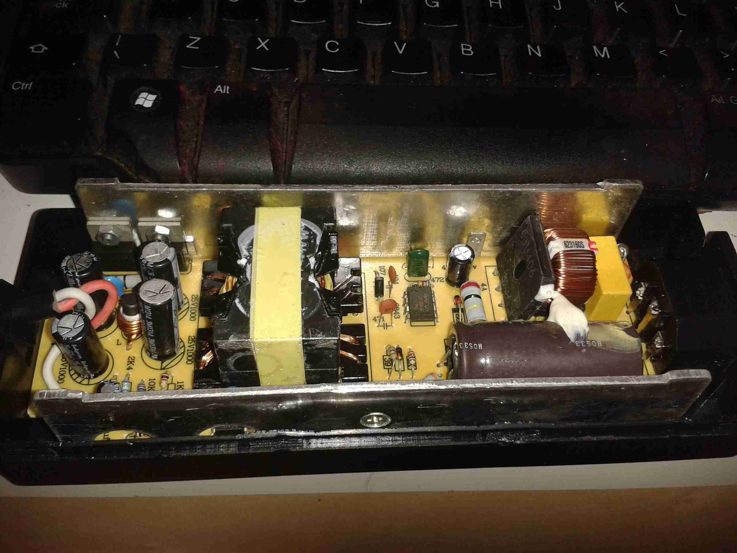
I recently ordered a PSU to run one of the TVs I converted to 12v operation, and being an older TV, it’s a fairly heavy load at 6.5A. eBay to the rescue again, with a cheap 10A rated supply.
Power Brick
Like all similar supplies these days, it’s a SMPS unit, and feels suspiciously light for it’s power rating.
Cover Removed
Luckily this one is easy to get into, no ultrasonic welding on the case, just clips. Here’s the top cover removed, big alloy plate between the heatsinks.
PCB
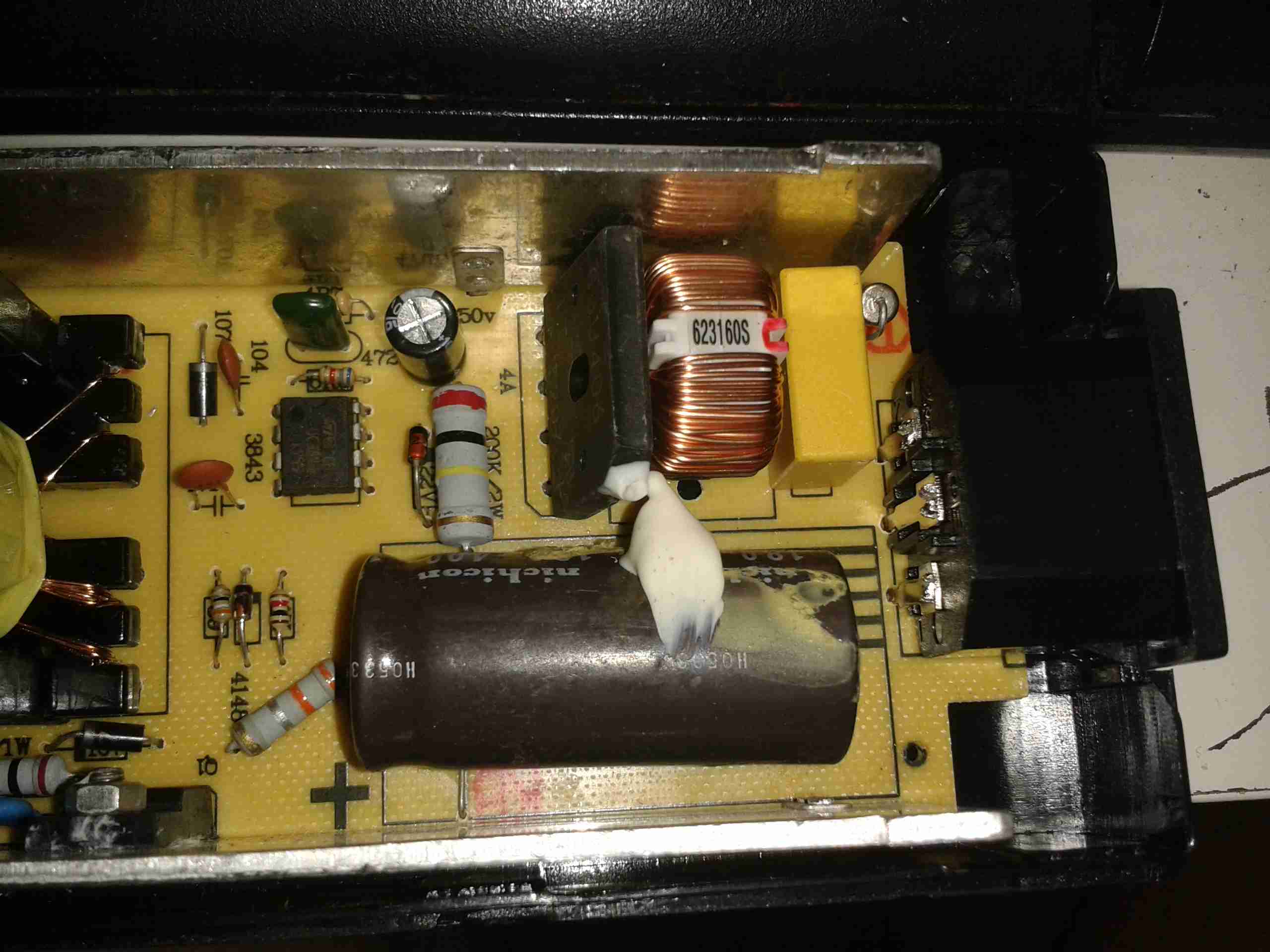
The top heatsink plate was glued to the top of the transformer with silicone, some gentle prying released it. From the top, things don’t look too bad. There’s some filtering on the mains input & it’s even fused!
Primary Side
Here’s a closeup of the primary side of the PSU, the main DC bus capacitor is a Nichicon one, but it’s clearly been recovered from another device, look at the different glue on the end!
it’s also flapping about in the breeze, the squirt of silicone they’ve put on does nothing to stop movement.
Also here is the mains input fuse, filter capacitor & common mode choke. At least there is some filtering!
The main control IC is a UC3843B High Performance Current Mode PWM Controller, operating at a switching frequency of 250kHz.
The main switching transistor is visible at the bottom left corner, attached to the heatsink.
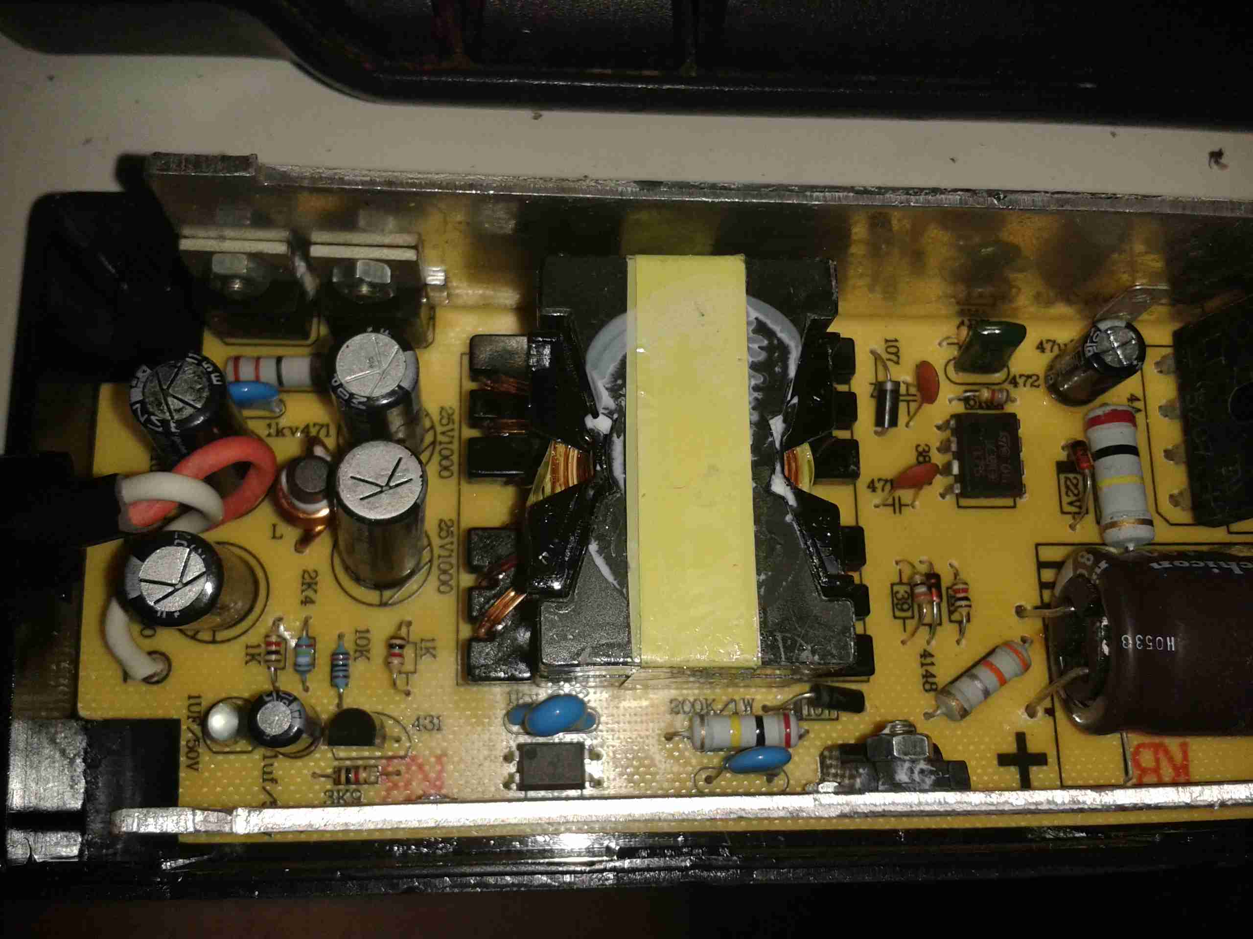
Secondary Side
Here’s the secondary side of the supply. The transformer itself is OK, nice heavy windings on the output to suit the high current.
It’s using proper opto-isolated feedback for voltage regulation, with a TL431 reference IC.
The output diodes are attached to the heatsink at the top of the photo, I couldn’t read any numbers on those parts.
The output filter capacitors are low quality, only time will tell if they survive. I’ll put the supply under full load & see what the temperature rise is inside the casing.
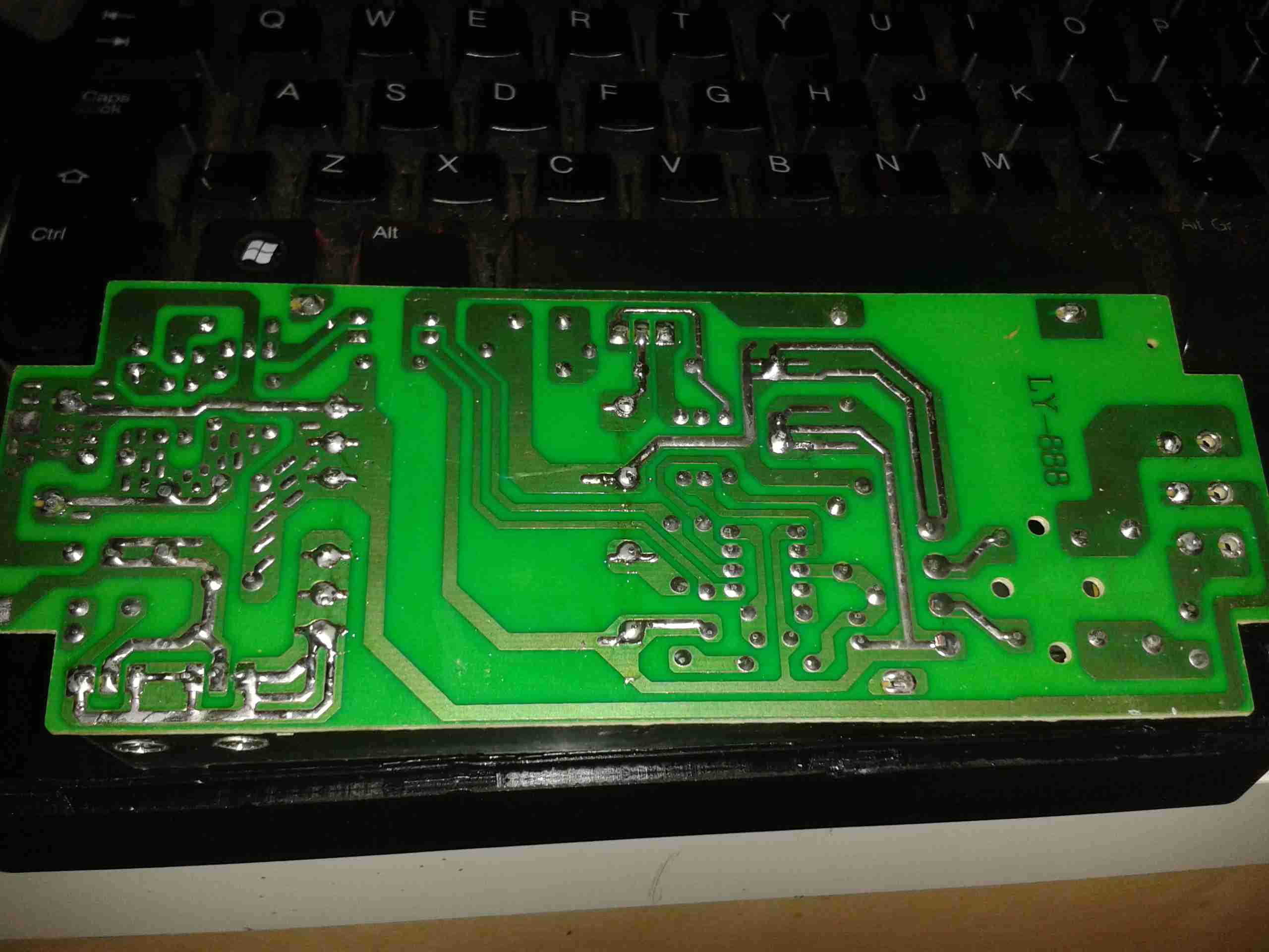
PCB Bottom
On the bottom of the PCB things get a little more dire. There isn’t really much of an isolation gap between the primary & secondary sides, and there’s a track joining the output negative with mains earth, which gets to within 2mm of the live mains input!
As with all these cheapo supplies, there’s good points & bad points, I will update when I’ve had a chance to put the supply under full load for a while & see if it explodes!
I recently dug out my other card printer to fit it with a 12v regulator, (it’s 24v at the moment), and figured I’d do a teardown post while I had the thing in bits.
This is a less industrial unit than my Zebra P330i, but unlike the Zebra, it has automatic duplexing, it doesn’t have Ethernet connectivity though.
Unlike domestic printers, which are built down to a price, these machines are very much built up to a spec, and feature some very high quality components.
Naked Printer
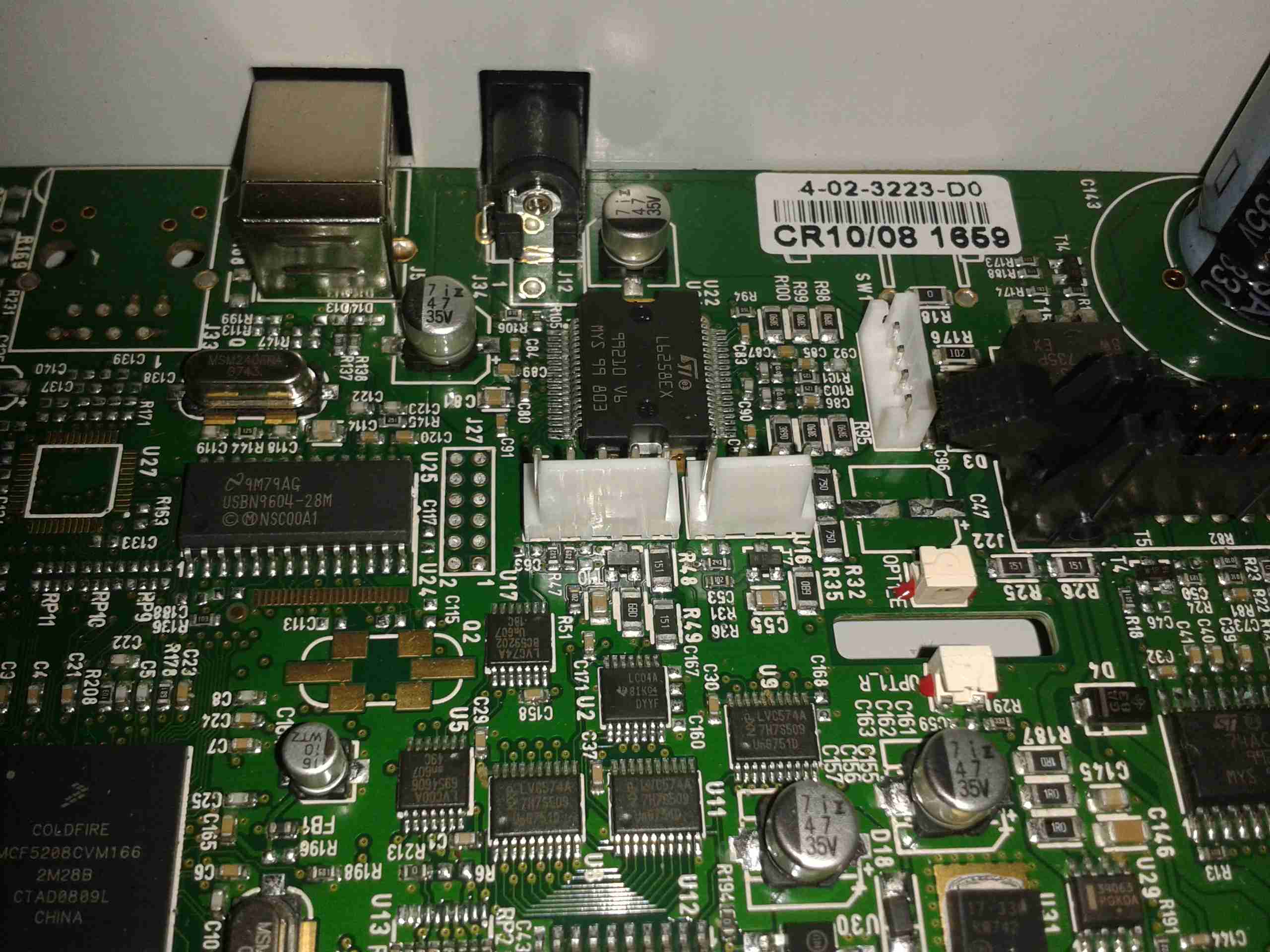
Here’s the mechanism with the cowling removed. This is the main drive side of the printer, with the main drive stepper at left, ribbon take-up spool motor lower right, and the duplex module stepper motors at far right.
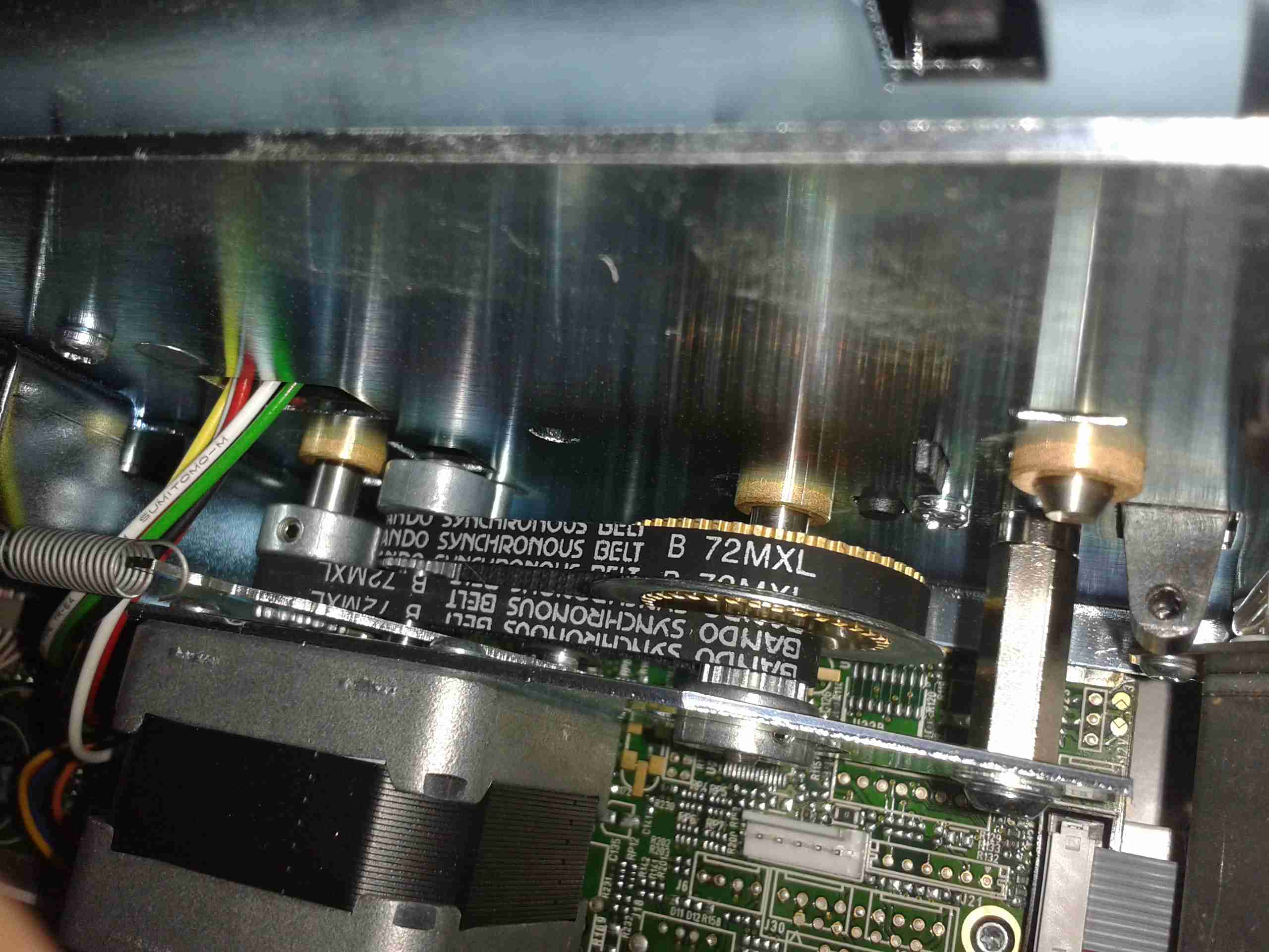
Main Motor Drive
The main drive motor runs the various rollers in the card path through a pair of synchronous belts, shown here.
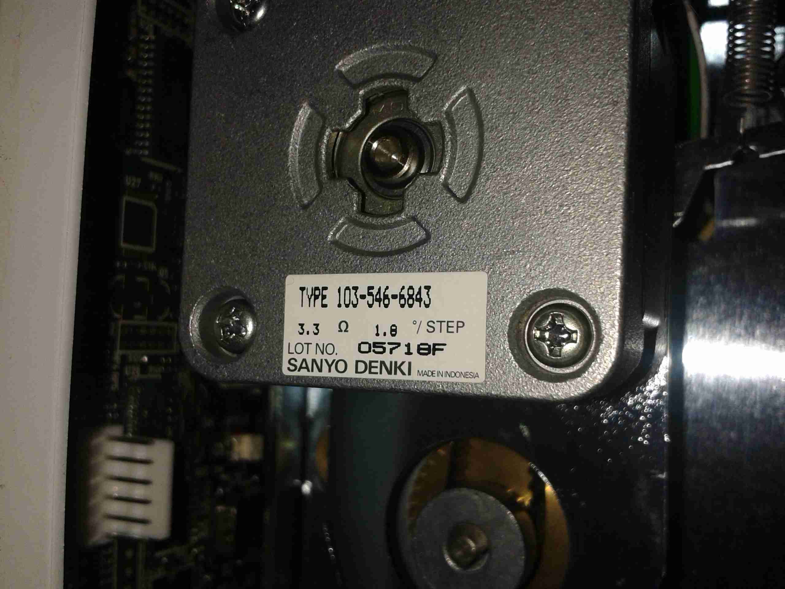
Main Stepper
The stepper itself is a quality ball-bearing Sanyo Denki bipolar motor.
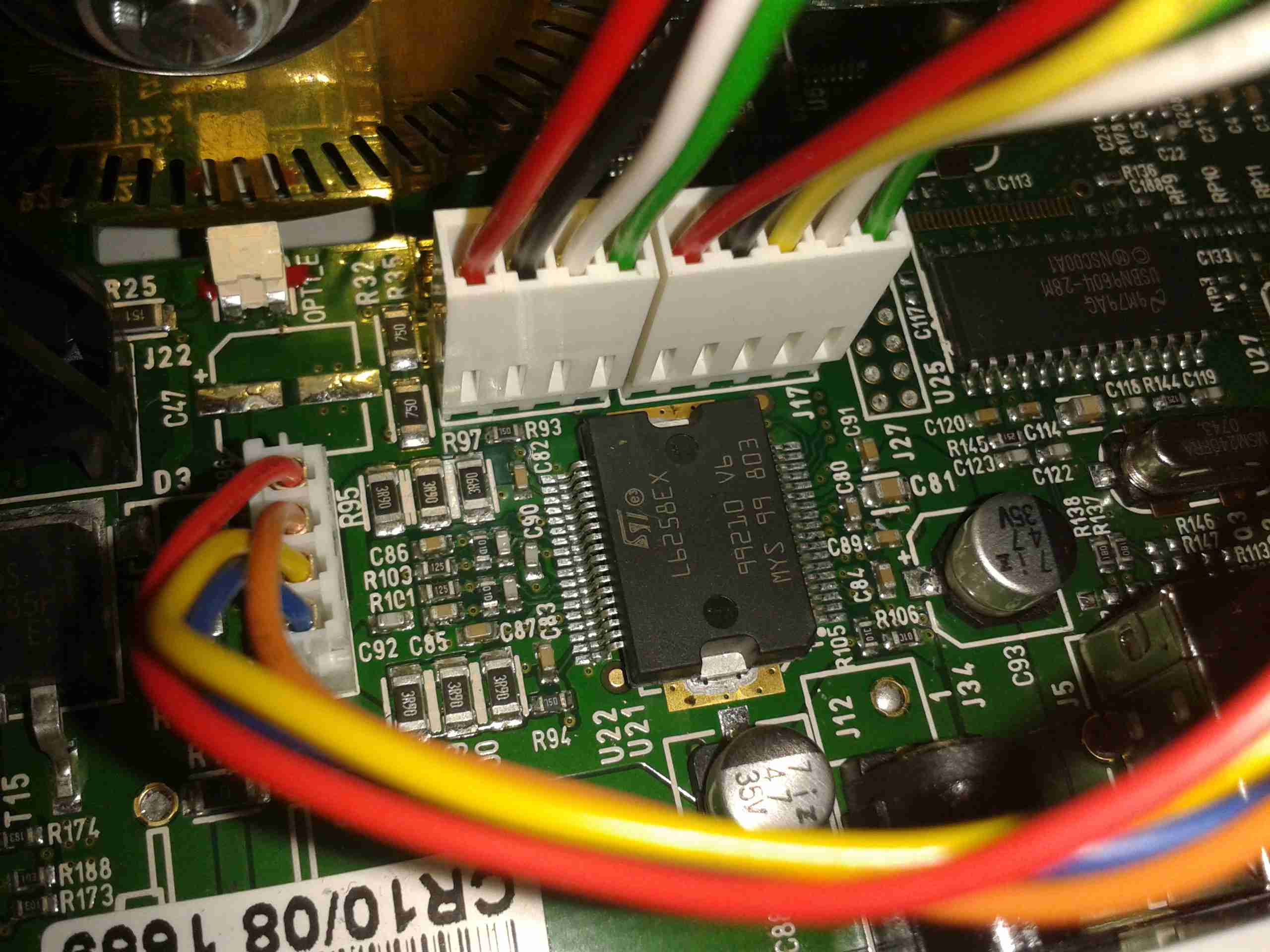
Main Stepper Driver
Electrical drive is provided to the stepper with a L6258EX DMOS universal motor driver. This chip can also drive DC motors as well as steppers.
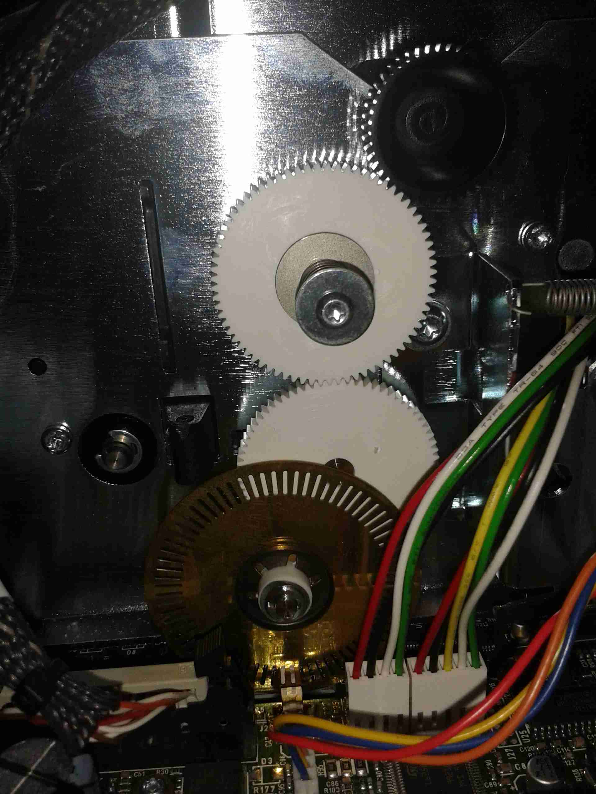
Ribbon Supply Spool
Here is the encoder geared onto the ribbon supply spool. This is used to monitor the speed the ribbon is moving relative to the card.
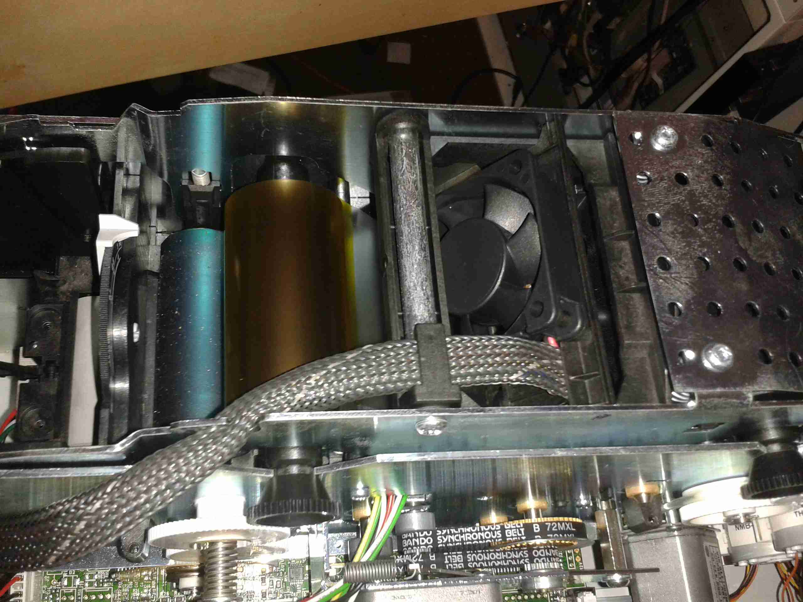
Printer Top
Here’s a top view through the printer, the blue roller on the left cleans the card as it’s pulled from the feeder, the gold coloured spool to it’s right is the ribbon supply reel. The cooling fan on the right serves to stop the print head overheating during heavy use.
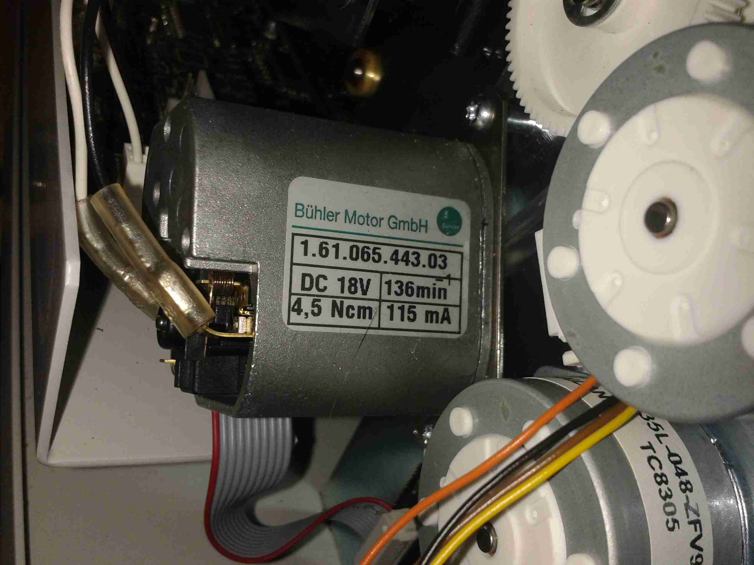
Spool Take Up Motor
The spool take-up reel is powered by another very high quality motor, a Buhler DC gearmotor. These printers are very heavily over engineered!
This motor drives the spool through an O-Ring belt, before the gear above. This allows the drive to slip in the event the ribbon jams, preventing it from breaking.
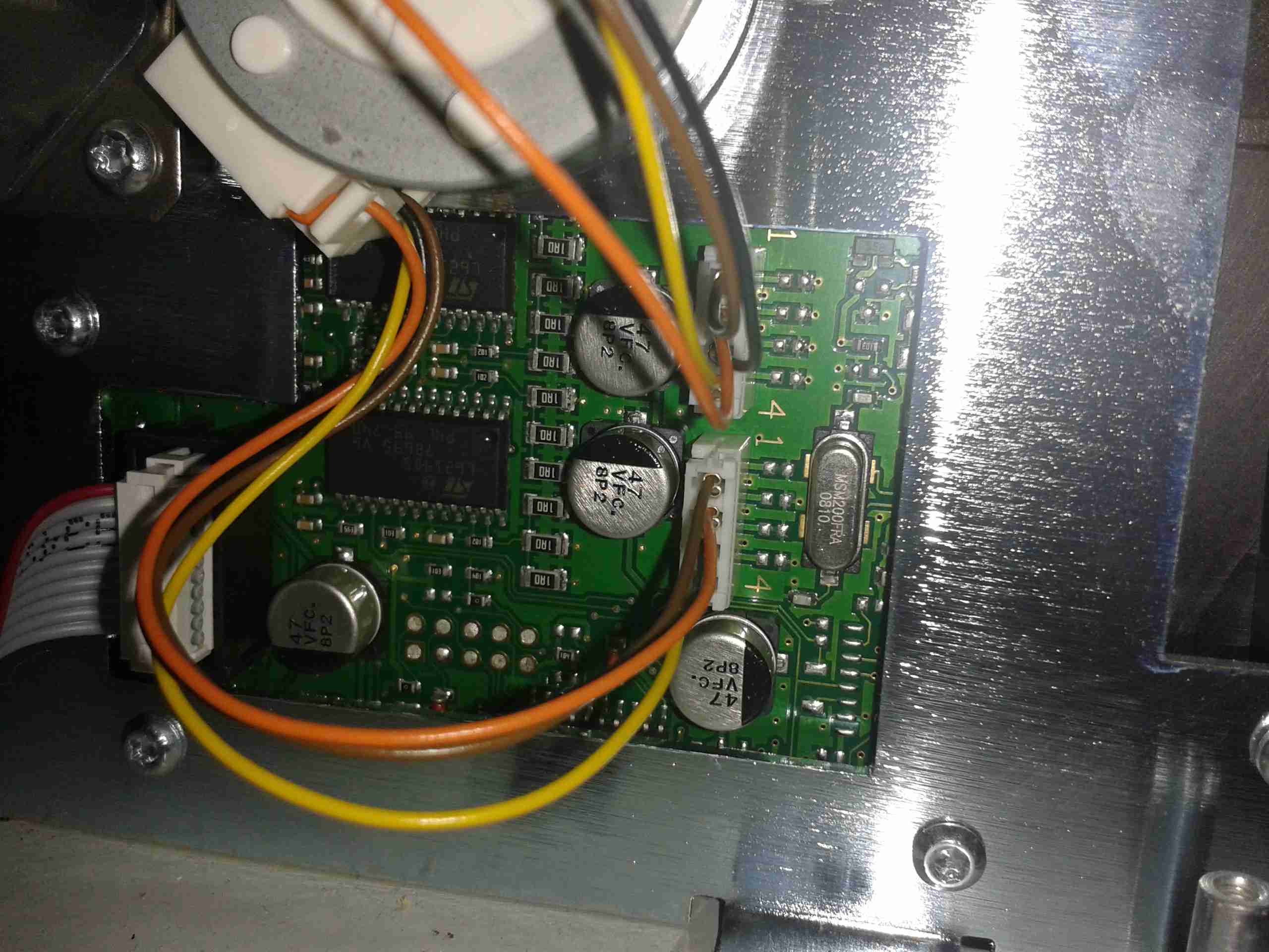
Duplex Unit Stepper Drivers
The pair of steppers that operate the duplexing unit are driven by a separate board, with a pair of L6219DS bipolar stepper driver ICs. There are also a couple of opto-sensors on this board for the output hopper.
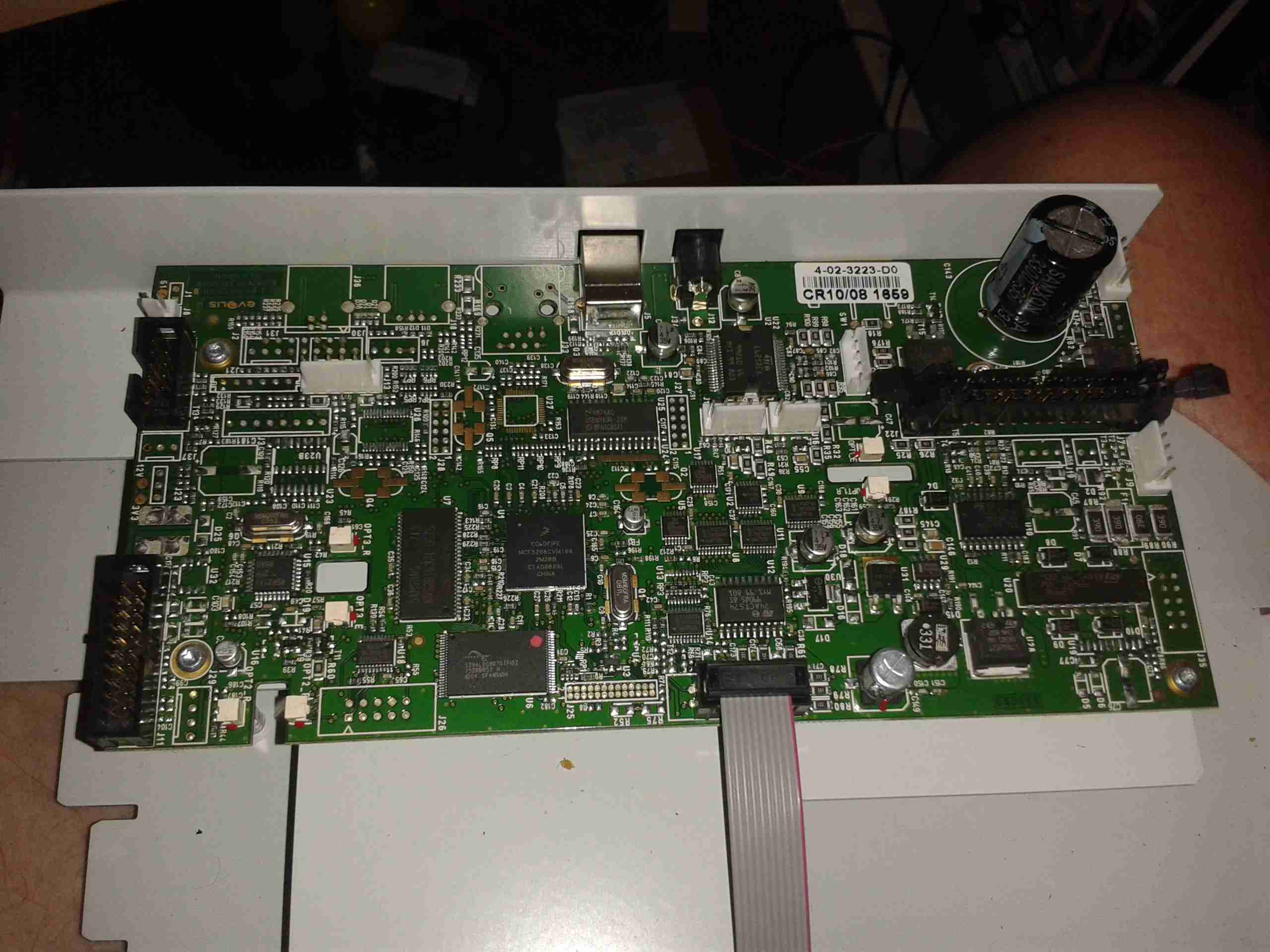
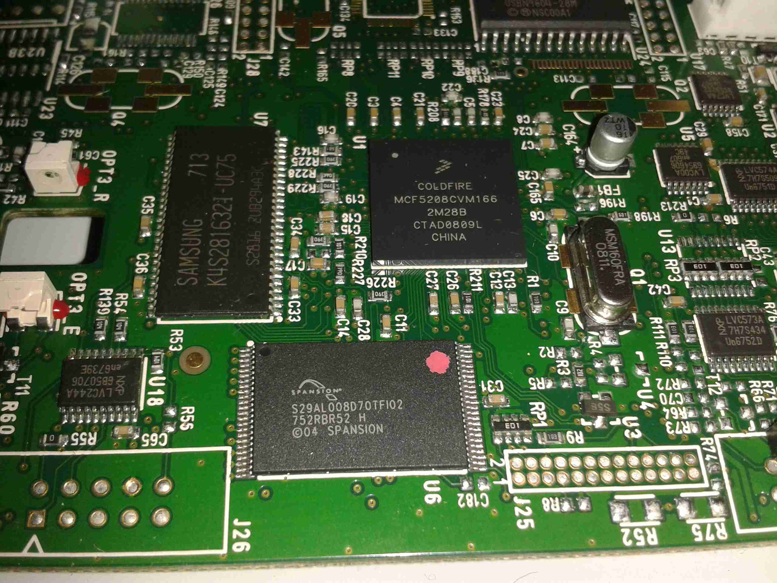
Main Control PCB
All the mechanisms of the printer are controlled from this main PCB, which handles all logic & power supply functions. Sections on the board are unpopulated, these would be for the Ethernet interface, smart card programming & magstripe programming.
Main CPU
The brains of the operation is this ColdFire MCF5208CVM166 32-bit microprocessor. It features 16KB of RAM, 8KB of cache, DMA controller, 3 UARTs, SPI, 10/100M Ethernet and low power management. This is a fairly powerful processor, running at 166MHz.
It’s paired with an external 128Mbit SDRAM from Samsung, and a Spansion 8Mbit boot sector flash, for firmware storage.
USB Interface & Power Input
Here the USB interface IC is located. It’s a USBN9604 from Texas Instruments, this interfaces with the main CPU via serial.
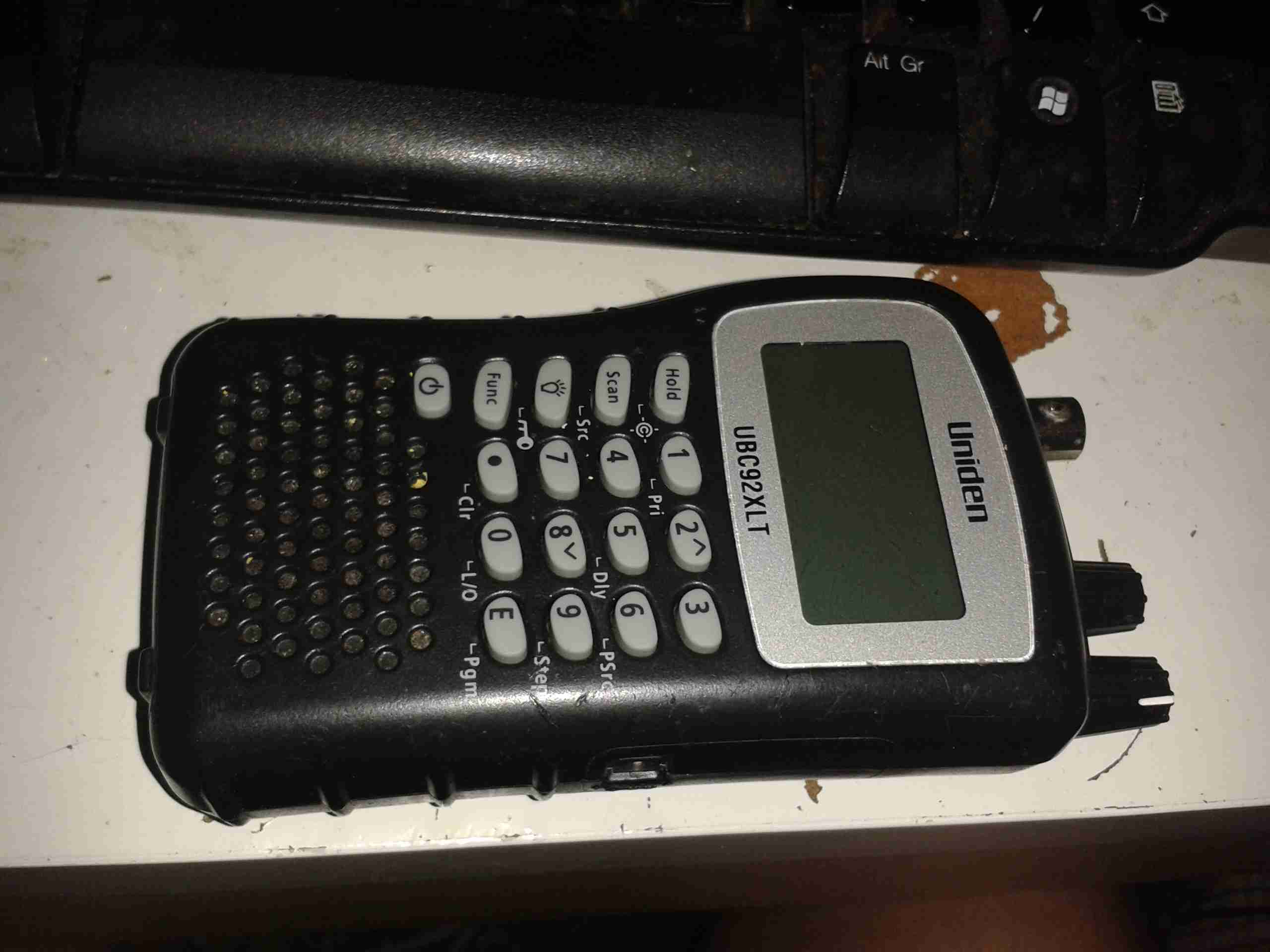
One bit of my equipment that I’ve never looked into is my scanner, a handheld Uniden unit. I got this when Maplin Electronics had them on special offer a few years ago.
Uniden Scanner
Here’s the scanner itself, roughly the same size as a usual HT.
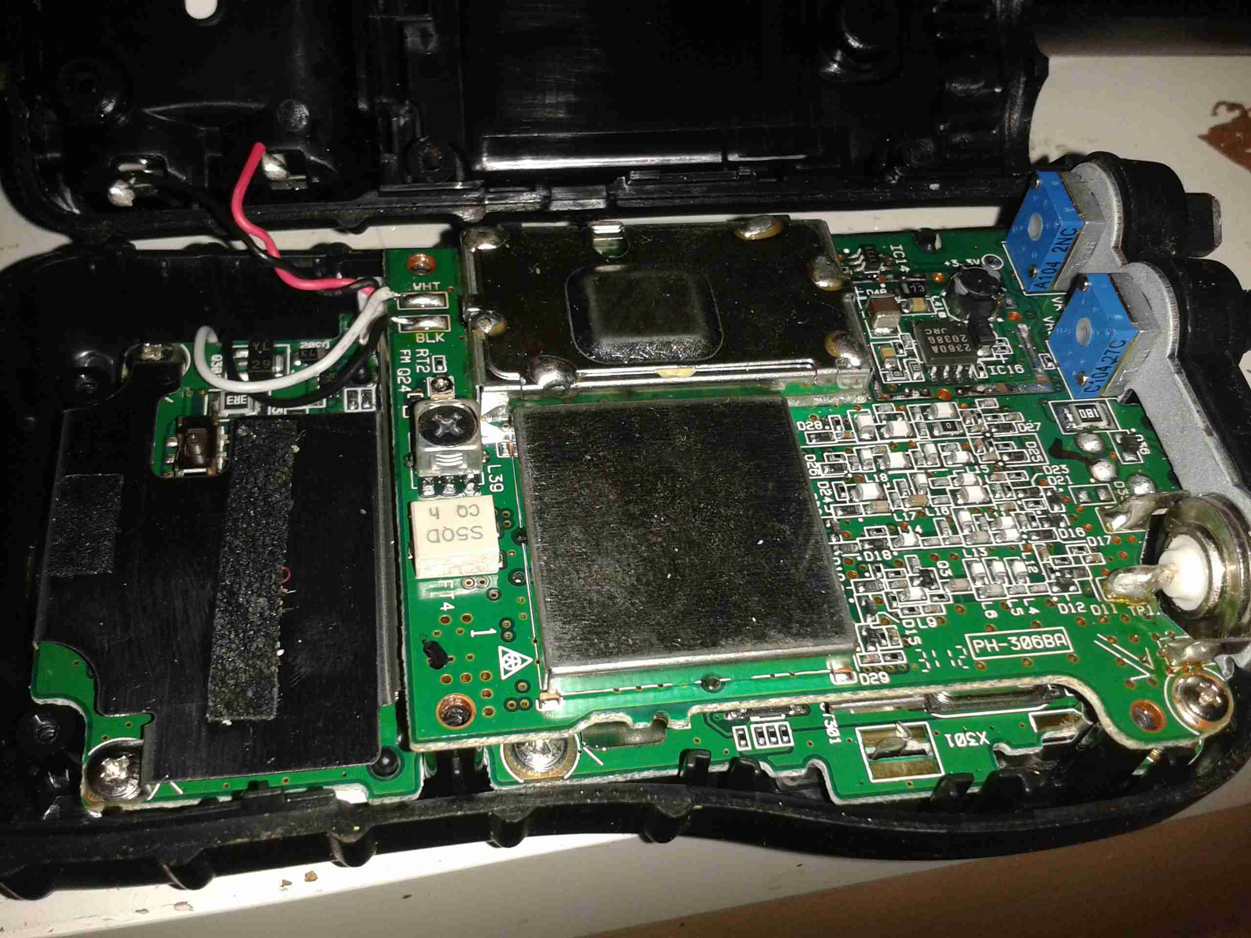
Back Cover Removed
Here the back cover has been removed, and the main RF board is visible at the top of the stack. Unfortunately the shielding cans are soldered on this unit, so no looking under there 🙁
On the right hand side of the board next to the antenna input is the main RF filter network, and it’s associated switching. The RF front end is under the shield closest to the front edge.
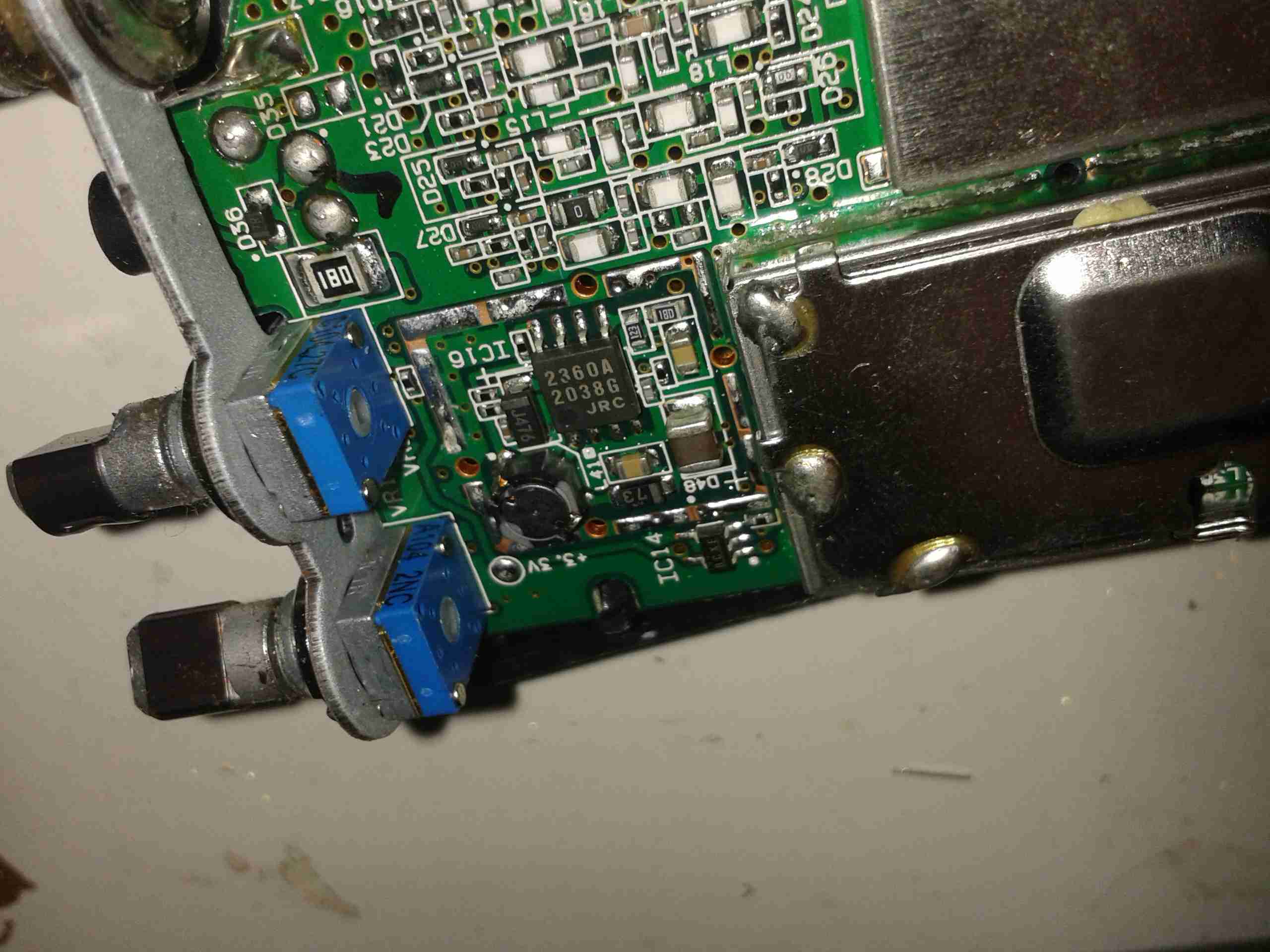
Controls & 3.3v Regulator
On the other side of the PCB is the Volume & Squelch potentiometers, along with a dedicated 3.3v switching supply. An NJM2360A High Precision DC/DC converter IC controls this one. A 3.3v test point is visible next to the regulator.
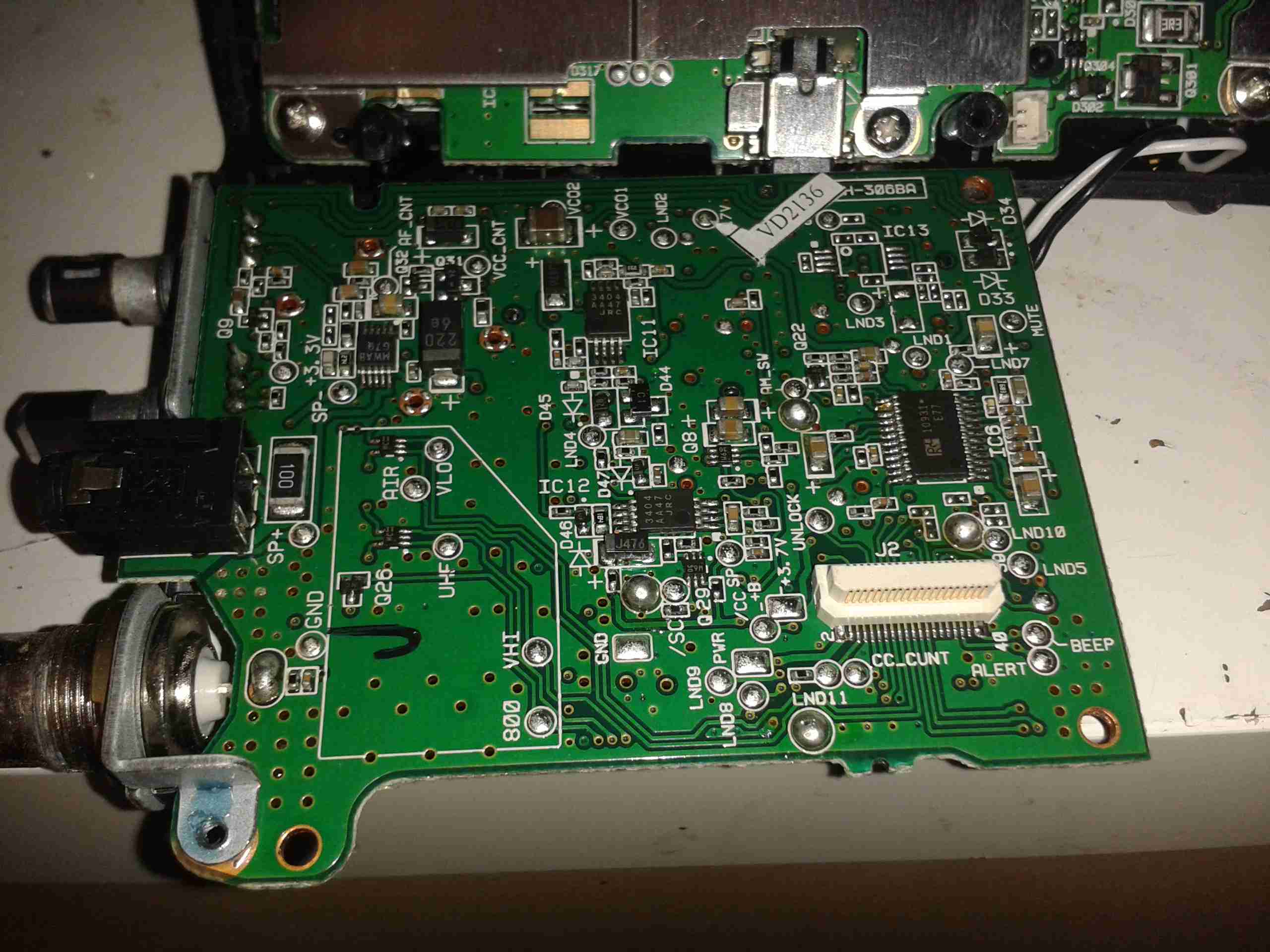
RF Board Reverse
Here’s the backside of the RF board, some more interesting parts here. There’s a pair of NJM3404A Single Supply Dual Op-Amp ICs, and a TK10931V Dual AM/FM IF Discriminator IC. This is the one that does all the back-end radio functionality. The audio amplifier for the internal speaker & external headphone jack is also on this PCB, top left. A board-to-board interconnect links this radio board with the main control board underneath.
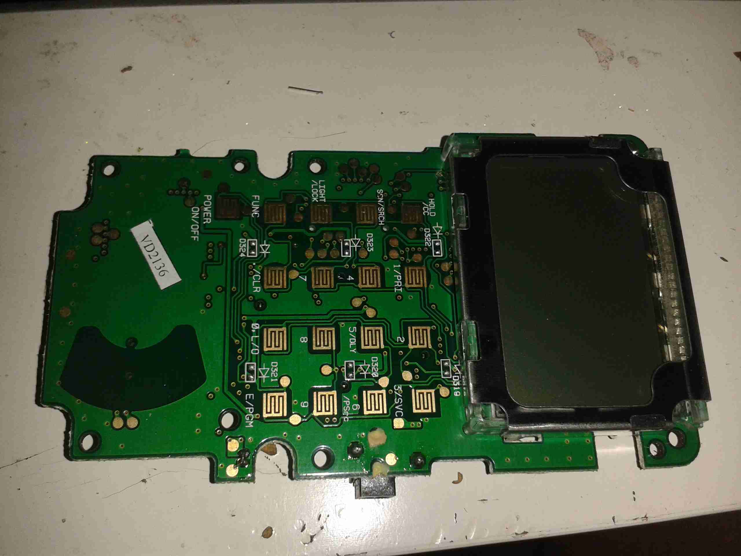
Control PCB Front
Here’s the front of the control PCB, nothing much to see here, just the LCD & membrane keypad contacts.
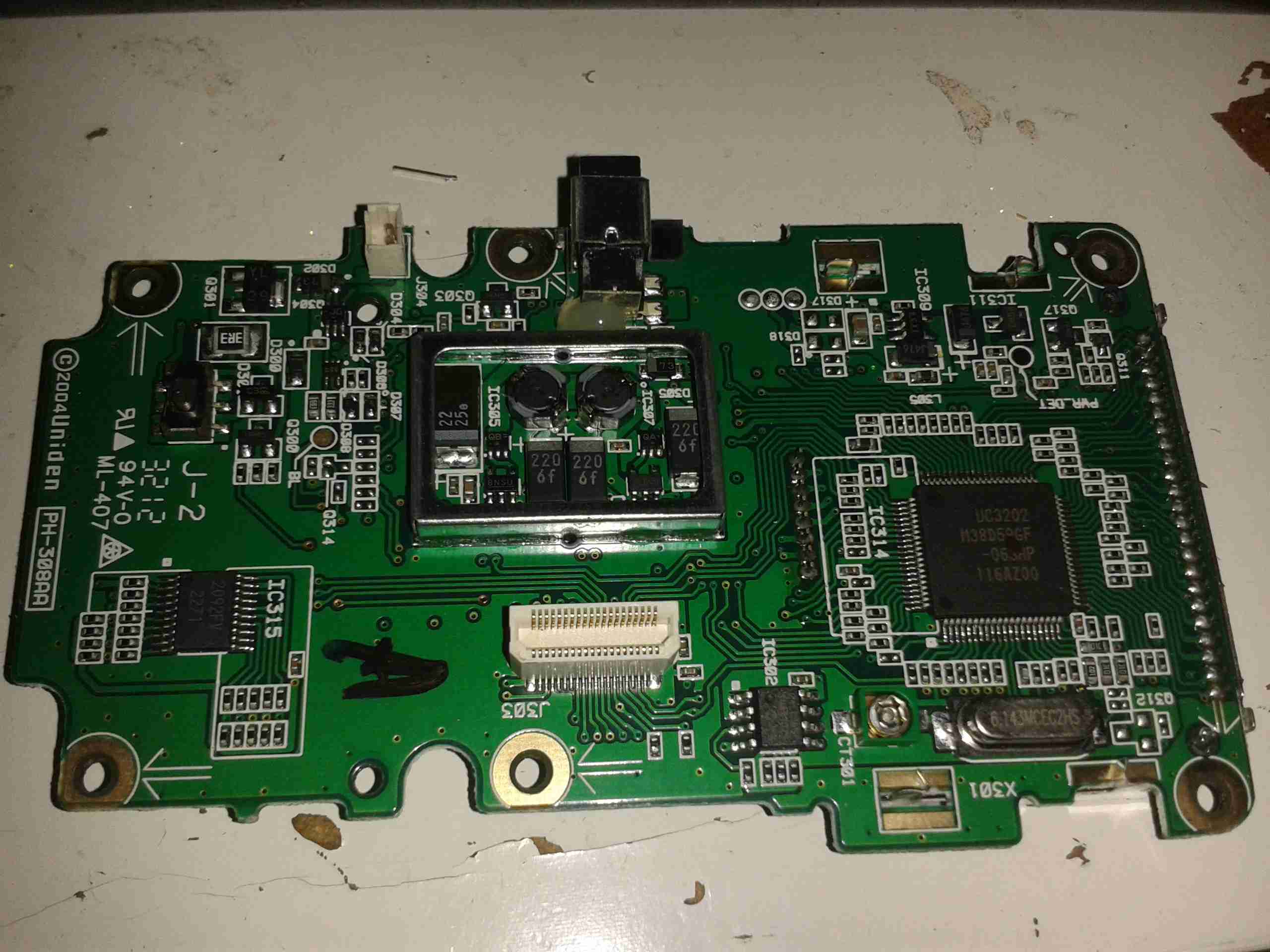
Control PCB Reverse
And here’s the reverse side of the control board. All the interesting bits are here. The main microcontroller is on the right, a Renesas M38D59GF, a fairly powerful MCU, with onboard LCD drive, A/D converter, serial interface, 60K of ROM & 2K of RAM. It’s 6.143MHz clock crystal is just below it.
The mating connector for the RF board is in the centre here.
There is also a Microchip 24LC168 16KB I²C EEPROM next to the main microcontroller. This is probably for storing user settings, frequencies, etc.
EEPROM
The rest of this board is dedicated to battery charging and power supply, in the centre is a dual switching controller, I can’t figure out the numbers on the tiny SOT23 components in here, but this is dealing with the DC 6v input & to the left of that is the circuitry for charging the NiMH cells included with the scanner.
PSU
The last bit of this PCB is a BU2092FV Serial In / Parallel Out 4 channel driver. Not sure what this one is doing, it might be doing some signal multiplexing for the RF board interface. Unfortunately the tracks from this IC are routed on the inner layers of the board so they can’t be traced out.
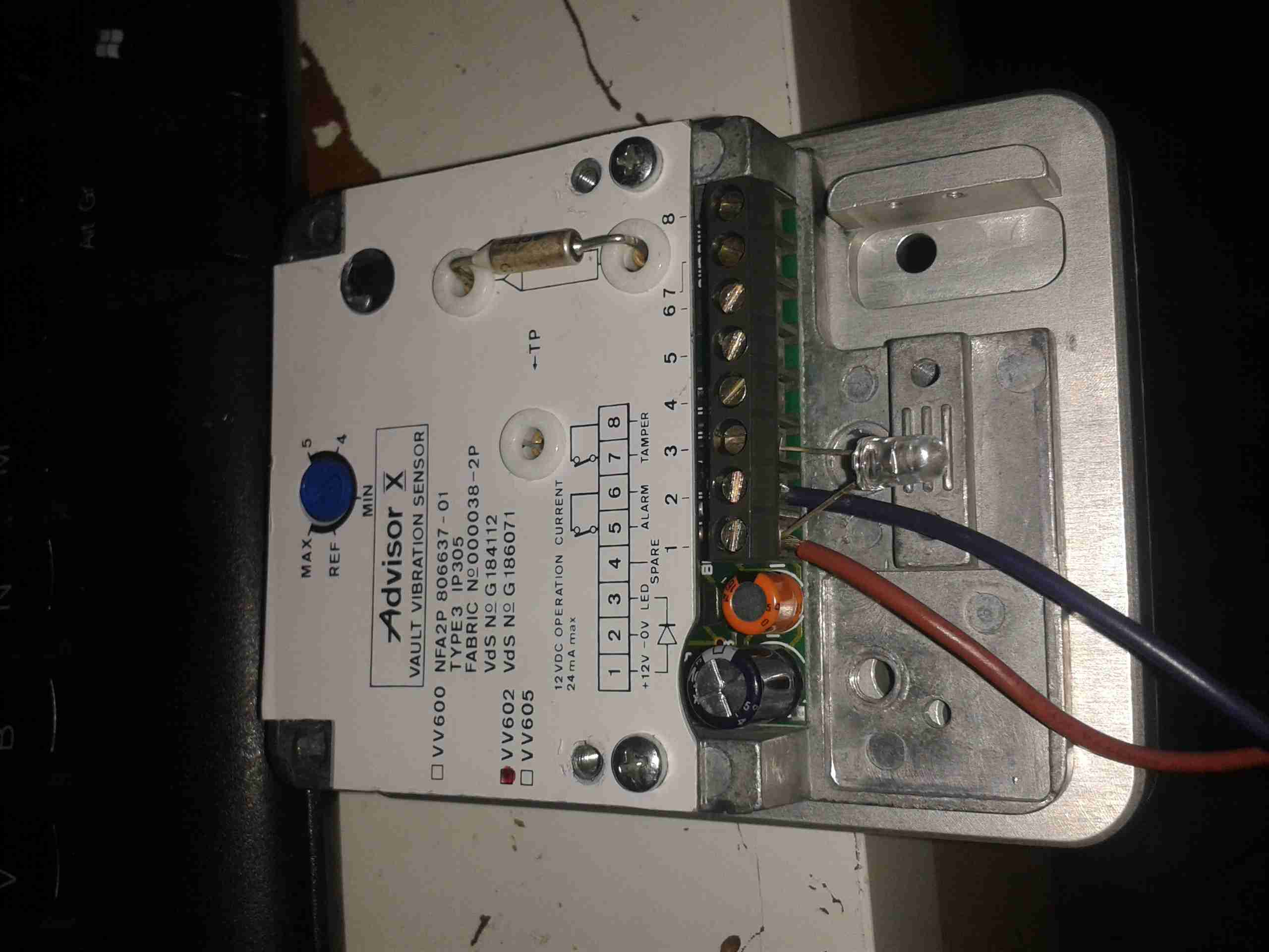
Here’s a rather unique device for protecting safes & vaults from attack by thefts.
It’s an Aritech VV602 seismic detector, based on piezoelectric sensors. Not surprisingly, this unit is covered in tamper sensors as well. There are several different sensor types in use:
Piezoelectric vibration sensing
Thermal sensing
Magnetic sensing
Manual Tamper Switches
Sensor Unit
Above is the main unit, with the thermal sensor. This is just a thermal fuse, very commonly used in everything from room heaters to hairdryers. This one triggers at 84°C. The adjustment pot is also visible here.
Mounting Plate
Above is the magnetic mounting plate used to attach the device to the safe. These units are apparently mounted over the keyhole of the safe to protect the lock, so they need to be easily removable to access the safe. This is a very strong magnet & it isn’t possible to pull it from a metal object without triggering the sensor.
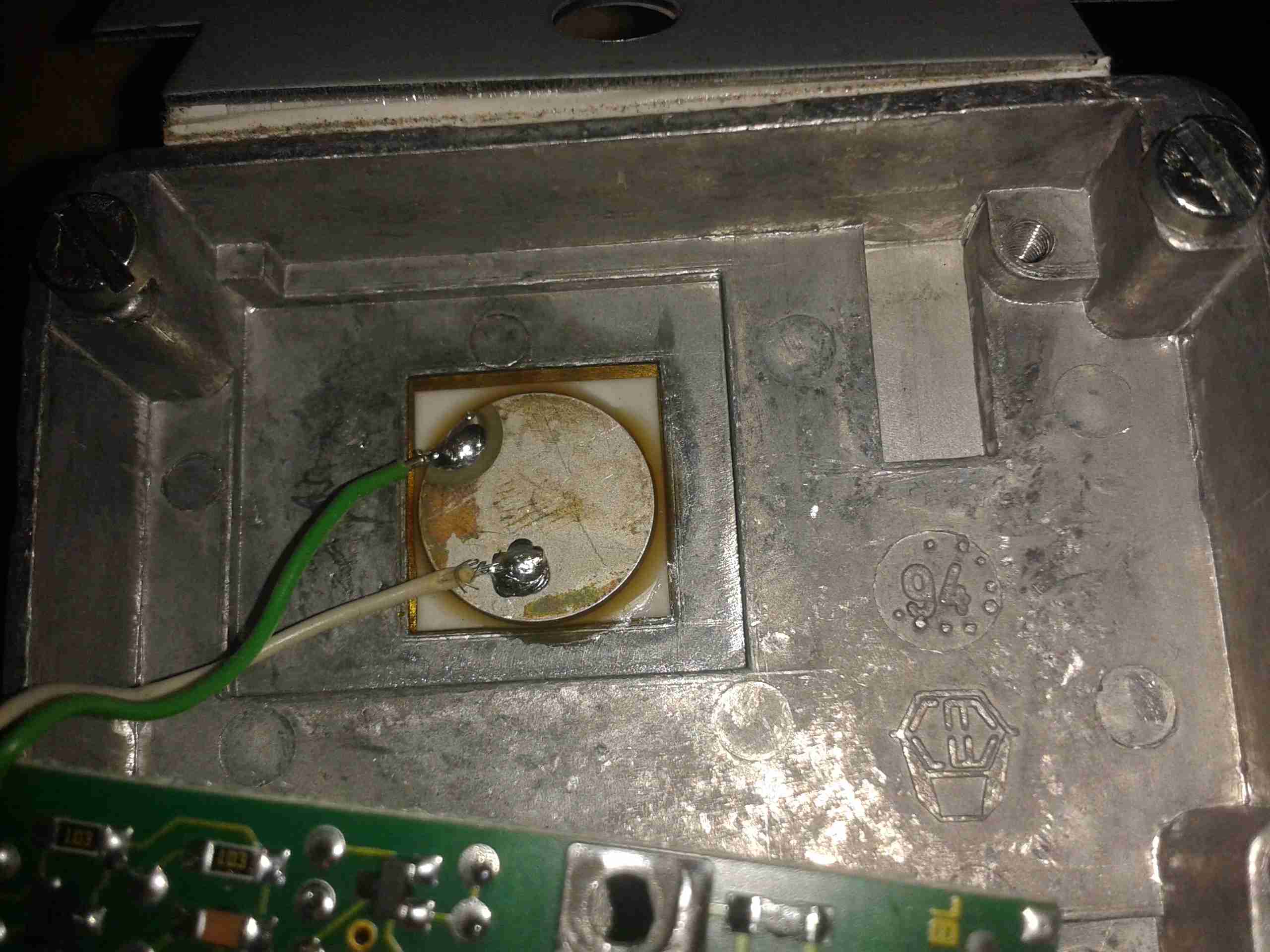
Piezo Sensor
Above is the piezo vibration sensor, bonded to the backplate. When the unit receives vibration or shock, this transducer generates a voltage, which is fed to the control logic below.
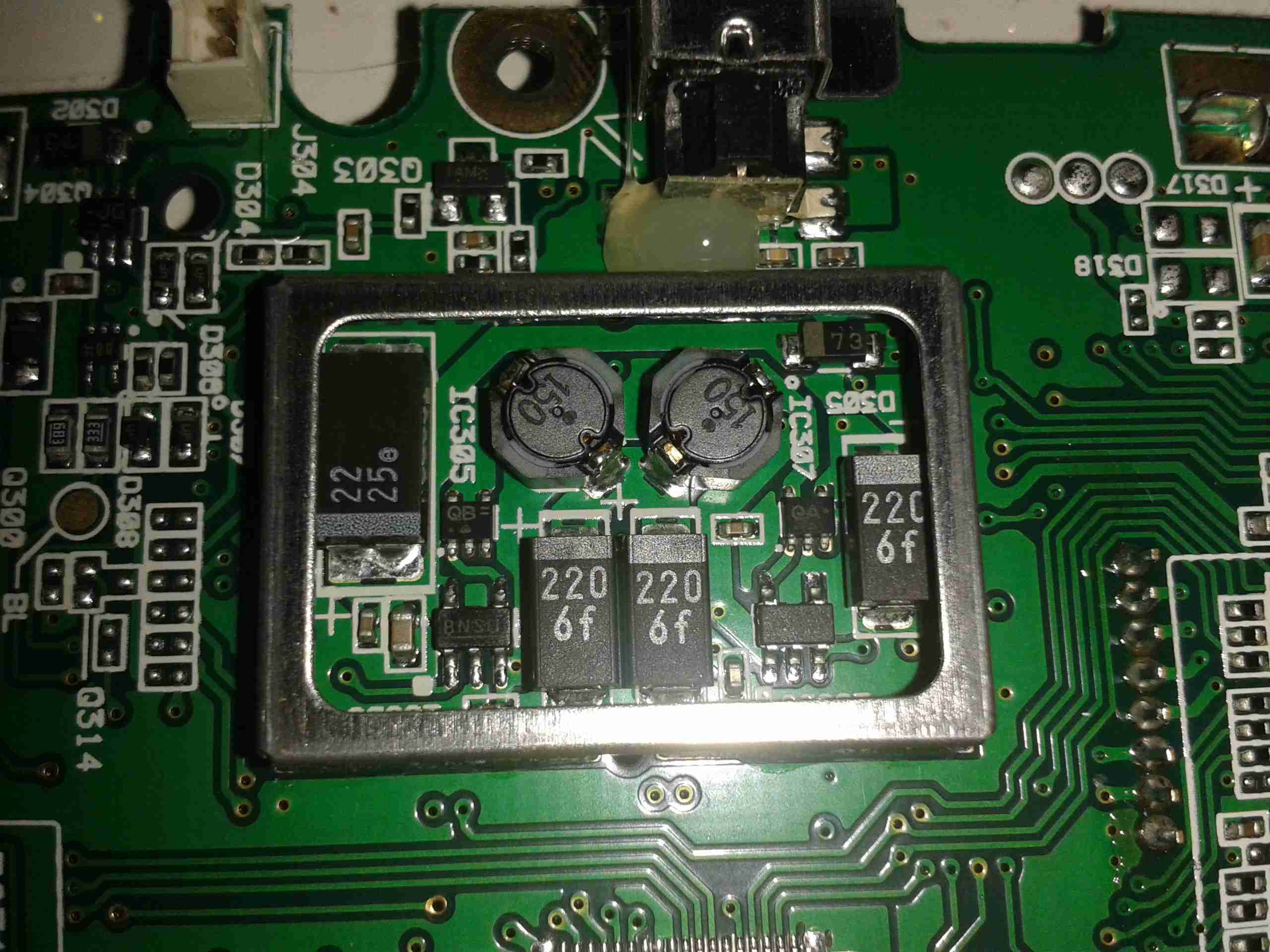
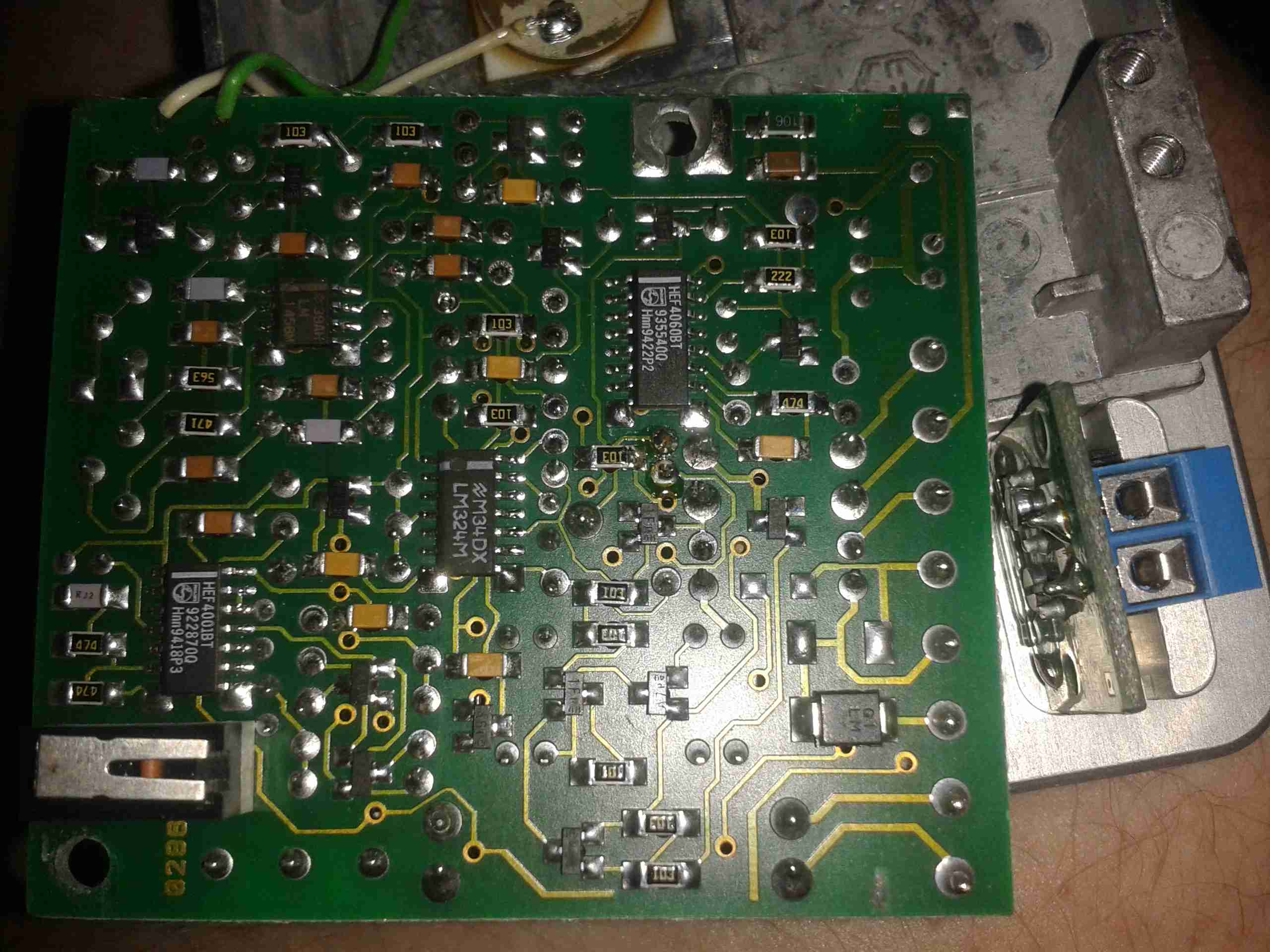
Control Logic
Here’s the reverse of the main PCB with the control logic ICs. These are basic logic gates, with a couple of comparators. One of the tamper switches is in the bottom left corner.
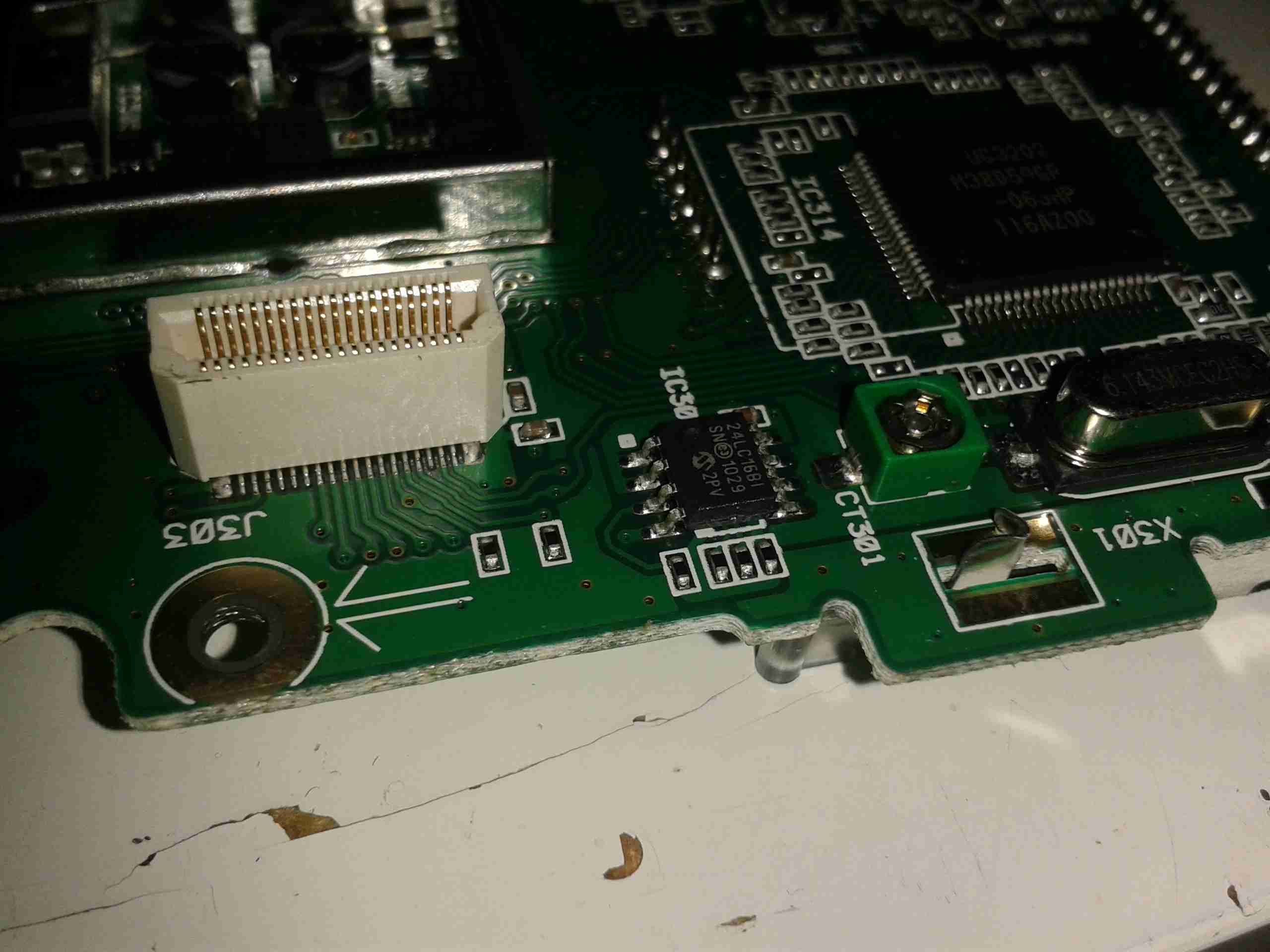
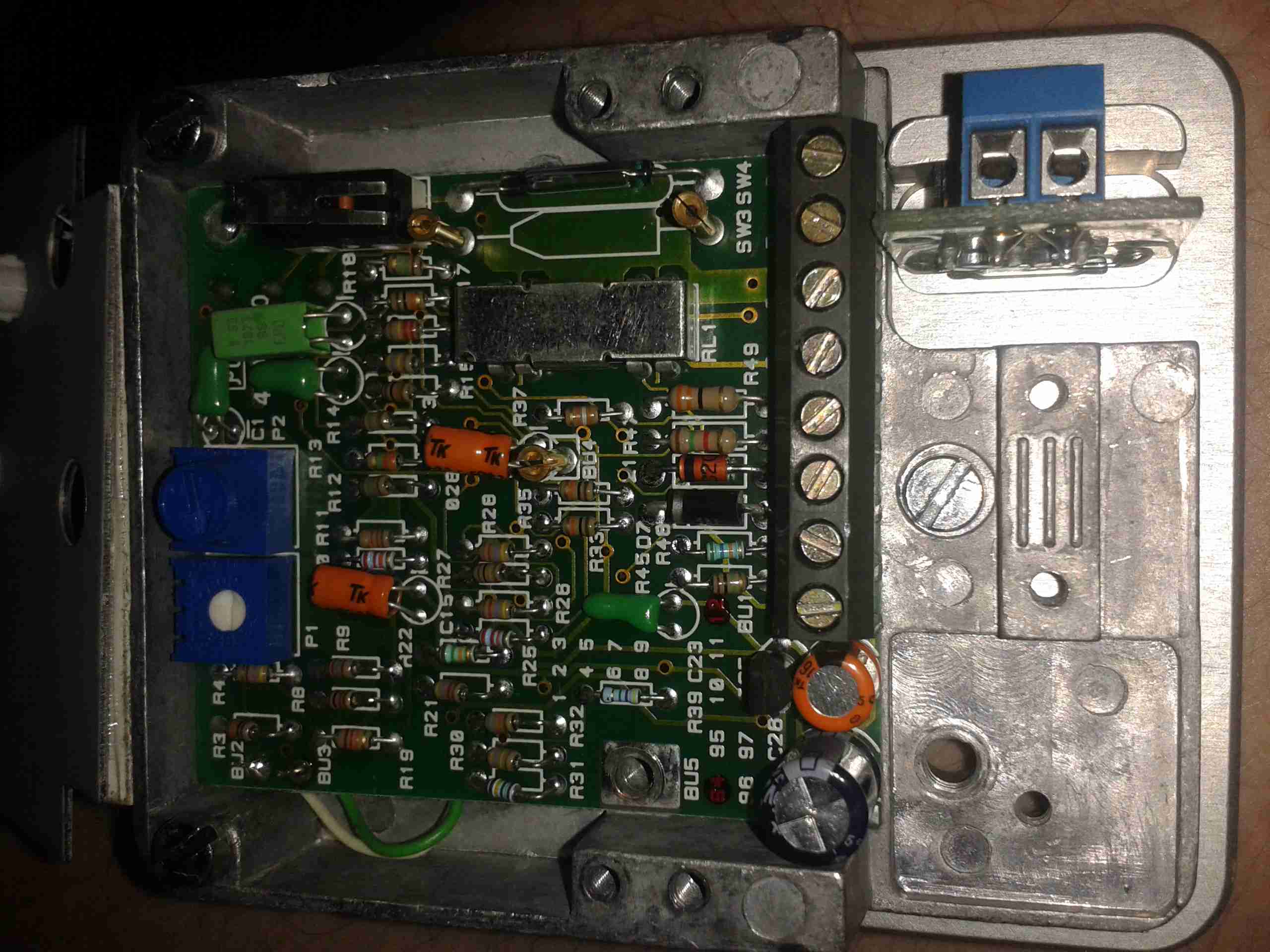
Main PCB
Main PCB with the connection terminals. Another tamper switch is in the top left corner, the solid-state relay is under the shield, next to the magnetic tamper switch. (Reed switch).
Some adjustment is provided for sensitivity. I’ve not found much of a difference in sensitivity though when it’s set to different levels.
Reed Tamper
Magnetic reed switch tamper on the right. Main output solid-state relay on the left under the shield.
This unit was given to me after it apparently went faulty. But on applying power it seems to work fine. Must be those experts again 😉
Tip Jar
If you’ve found my content useful, please consider leaving a donation by clicking the Tip Jar below!
All collected funds go towards new content & the costs of keeping the server online.