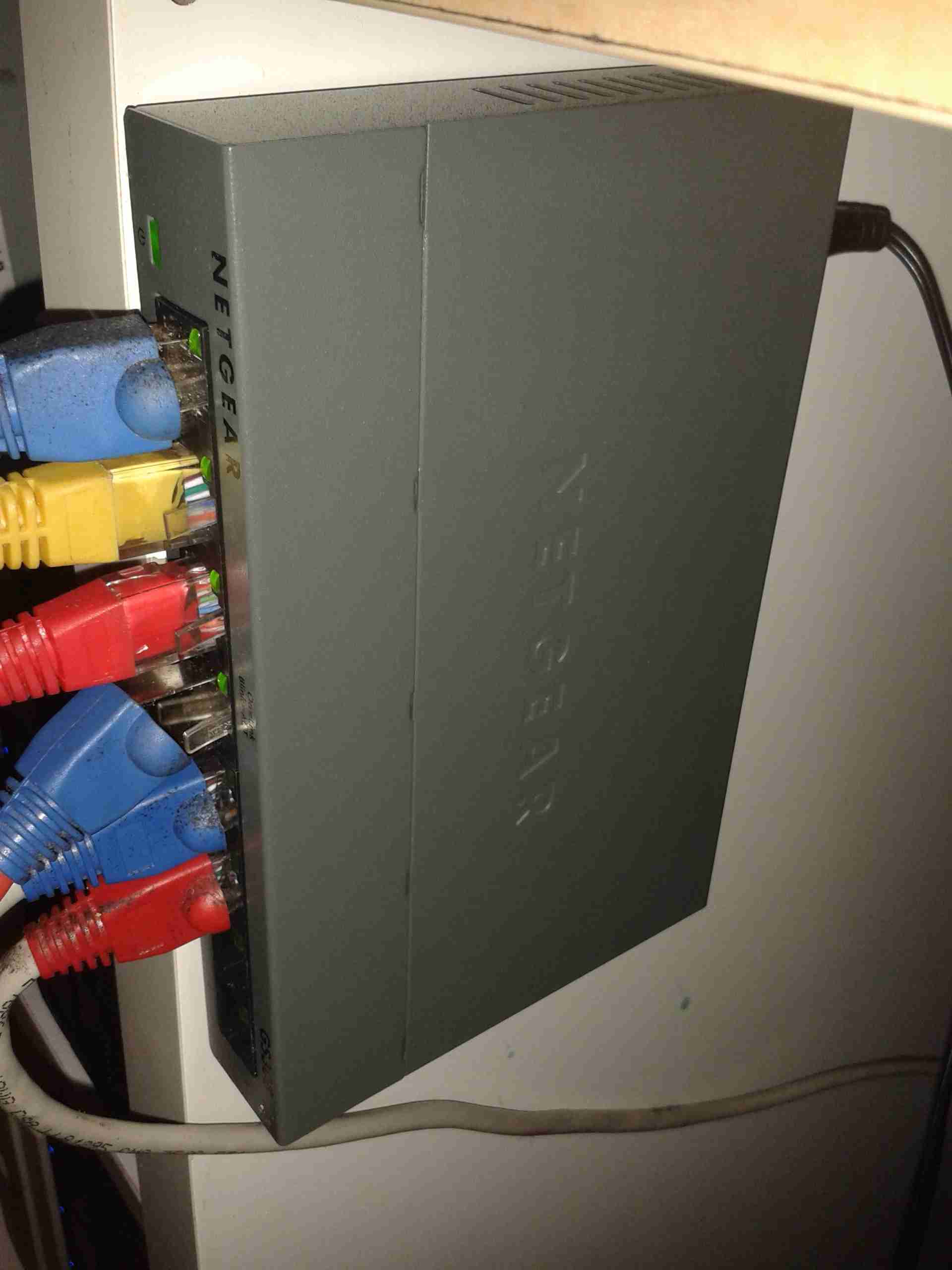
Here’s a new addition to the network, mainly to replace the ancient Cisco Catalyst 3500 XL 100MB switch I’ve been using for many years, until I can find a decently priced second hand commercial gigabit switch.
Operational
Here’s the switch with some network connections on test. So far it’s very stable & draws minimum power. I’ve not yet attempted to run my core links (NAS) through yet, as I’ve not yet seen a consumer grade switch that can stand up to constant full load without crashing.
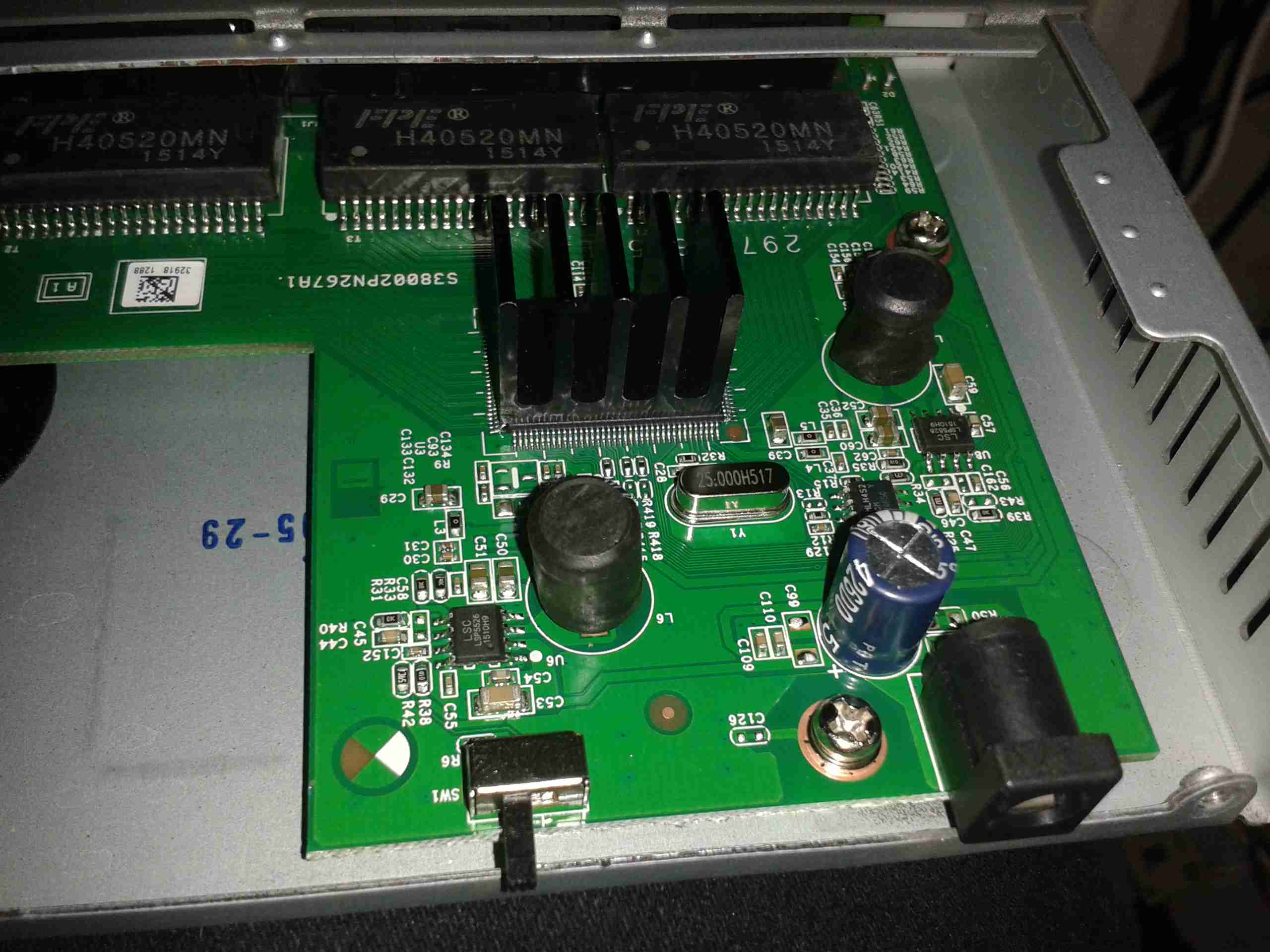
Internals
Here’s the switch with it’s lid popped. The magnetics can be seen at the back, next to the RJ-45 ports, the large IC in the centre is the main switching IC, with a heatsink bonded to the top. Very minimal design, with only a couple of switching regulators for power supply & not much else.
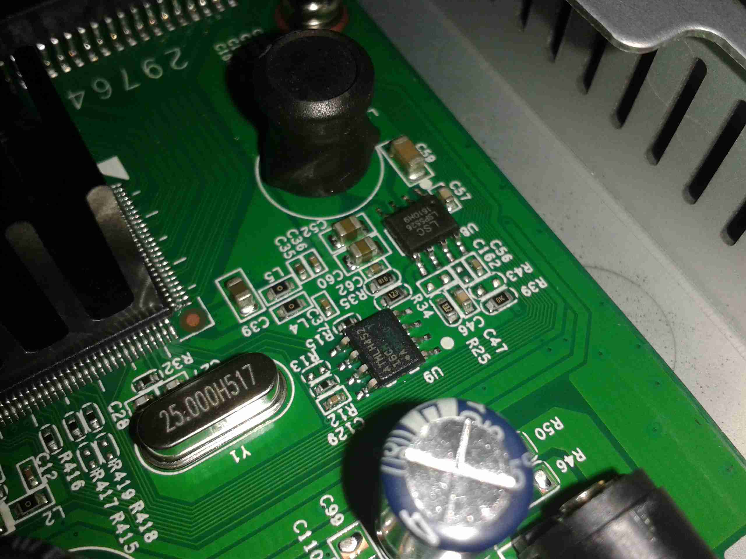
Power & EEPROM
Here’s a closeup of some of the support components. There’s a 25MHz crystal providing a clock signal for the switch IC, just to the right of that is an EEPROM. I imagine this is storing the switch configuration & MAC address. Further right is one of the switching DC-DC converter ICs for power.
As a quick test, here’s 500GB of data being shifted through the switch, at quite an impressive rate. I’m clearly maxing out the bandwidth of the link here. Soon I will upgrade to a 10G Ethernet link between the NAS & main PC to get some more performance.
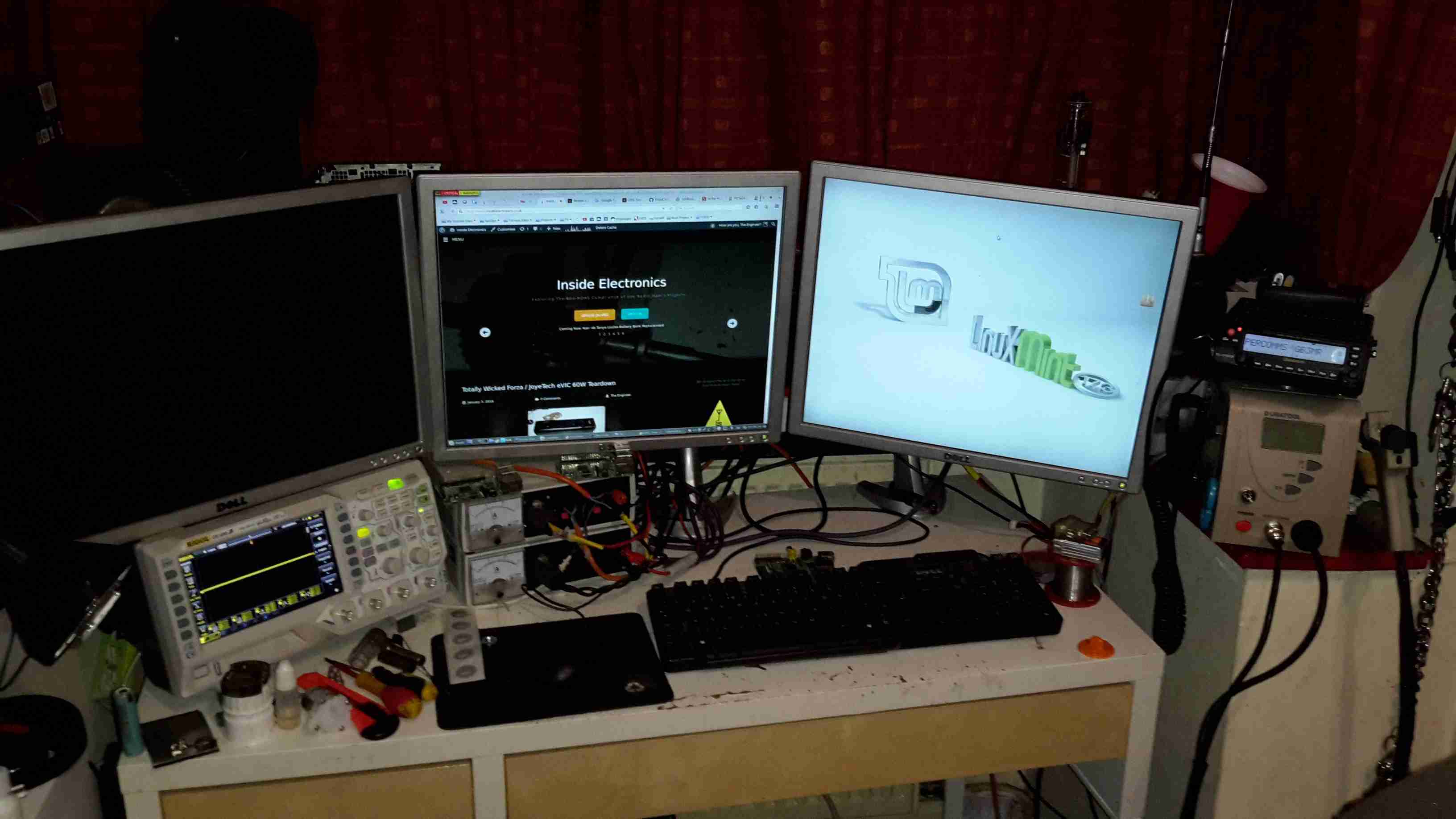
Main radio of course is housed on the left, it’s partially hidden under my currently over-populated breadboard.
All 3 monitors are linked to the same PC, using a pair of video cards. This is a very flexible system with so much screen real estate.
Main system power is provided by the pair of power supplies next to the radio – these are homebrew units using surplus switched mode PSU boards. Check my previous posts for more details.
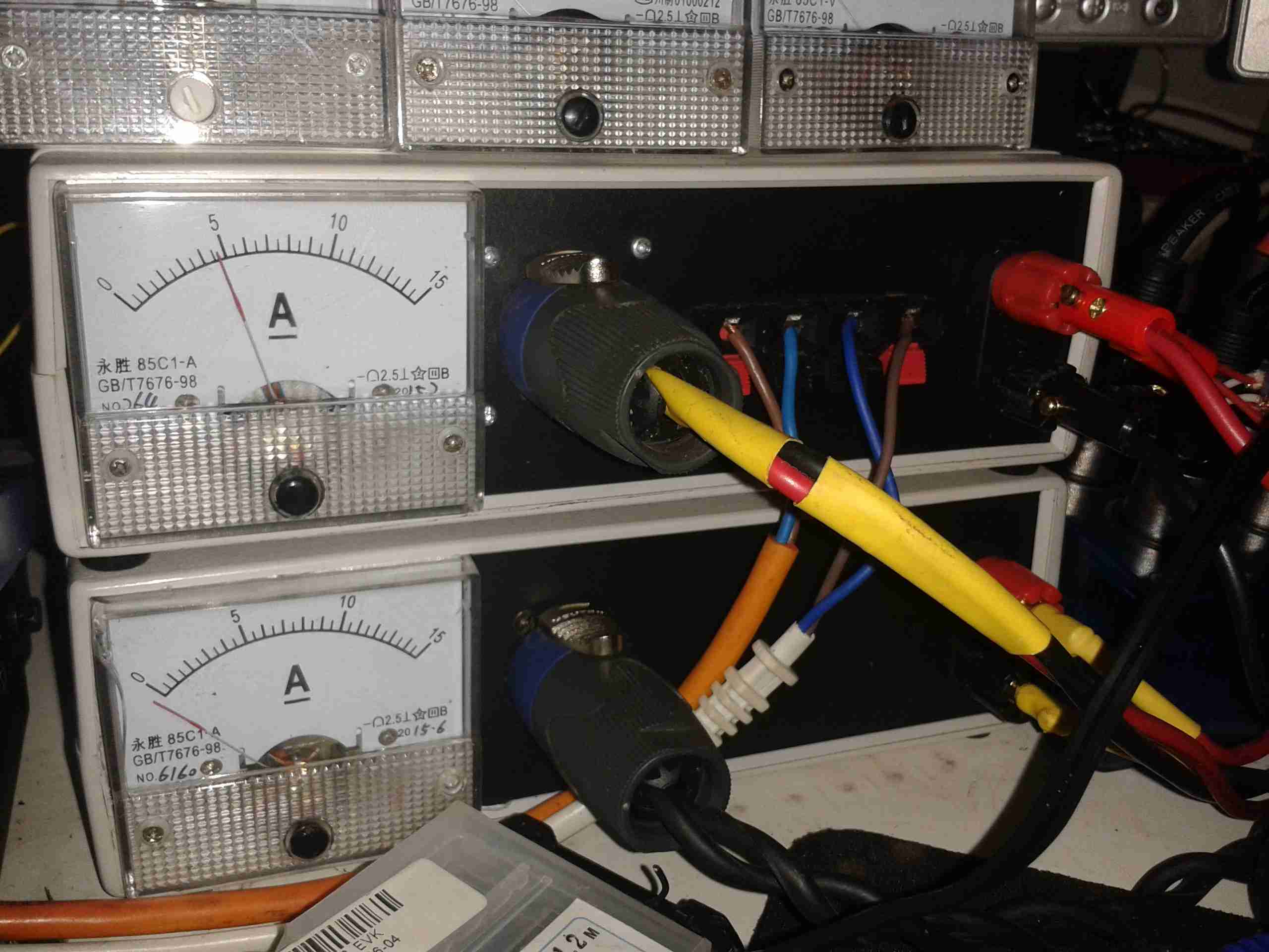
Power Supplies
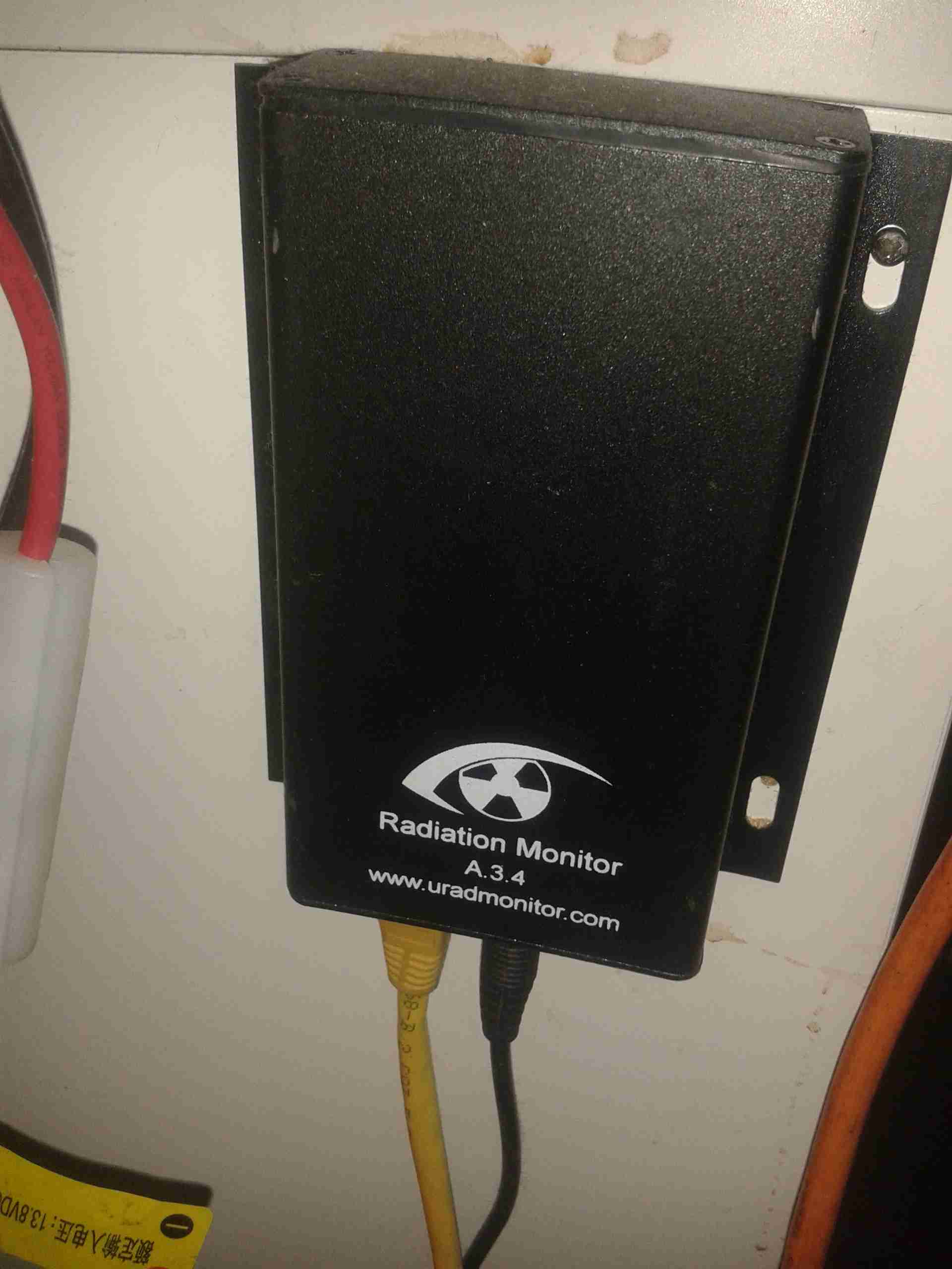
The mainpowersupply system. These two supplies are cross connected, giving a total DC amperage of 30A at 13.8v. There is also a link to a large 220Ah lead-acid battery bank (orange cable), to keep me on the air during power outages. This cable is getting upgraded to something more beefy shortly. The white cable is currently supplying power to my onlineradiation monitor.
The main high-currentDC outputs are the Speakon connectors next to the meters. The top one is powering the radio directly, the bottom is linked through to my 12v distribution box for lower current loads, such as the oscilloscope, audio amplifiers, tools, etc.
Radiation Monitor
Attached to the side of the desk is the radiation monitor itself.
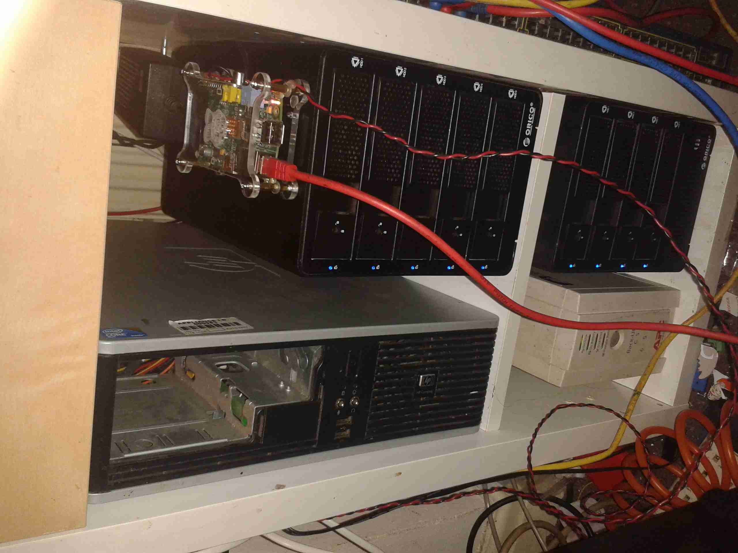
Core NAS
Under the radio is the core NAS of the network. It’s an array of 9 4TB disks, in RAID6, giving a total capacity after parity of 28TB. This provides storage & services to every other machine in the shack, the Raspberry Pi on top of the disk array is doing general network housekeeping & monitoring, also generating the graphs for the Radiation Monitor page. A Cisco 48-portswitch is partially out of frame on the right, providing 100MB Ethernet to the devices that don’t require gigabit.
My other monitors are a different model, and have a slightly different main PCB inside, but the process is mostly the same for converting these to 12v supply.
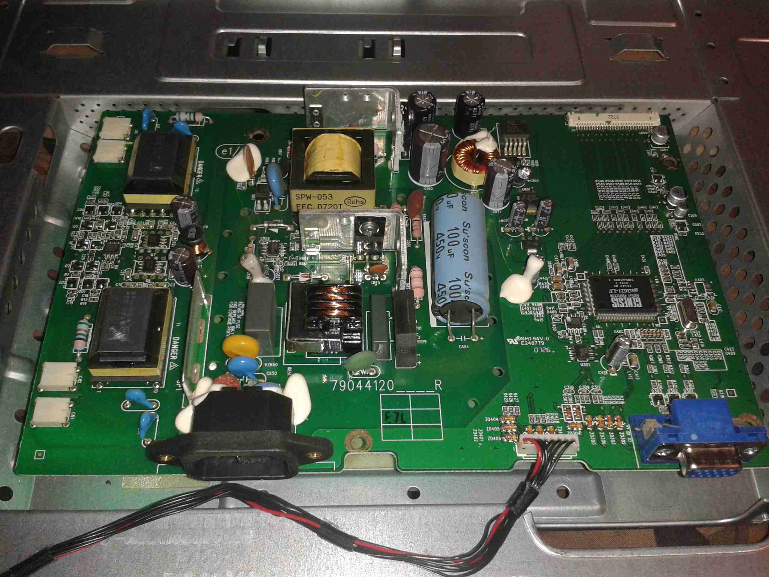
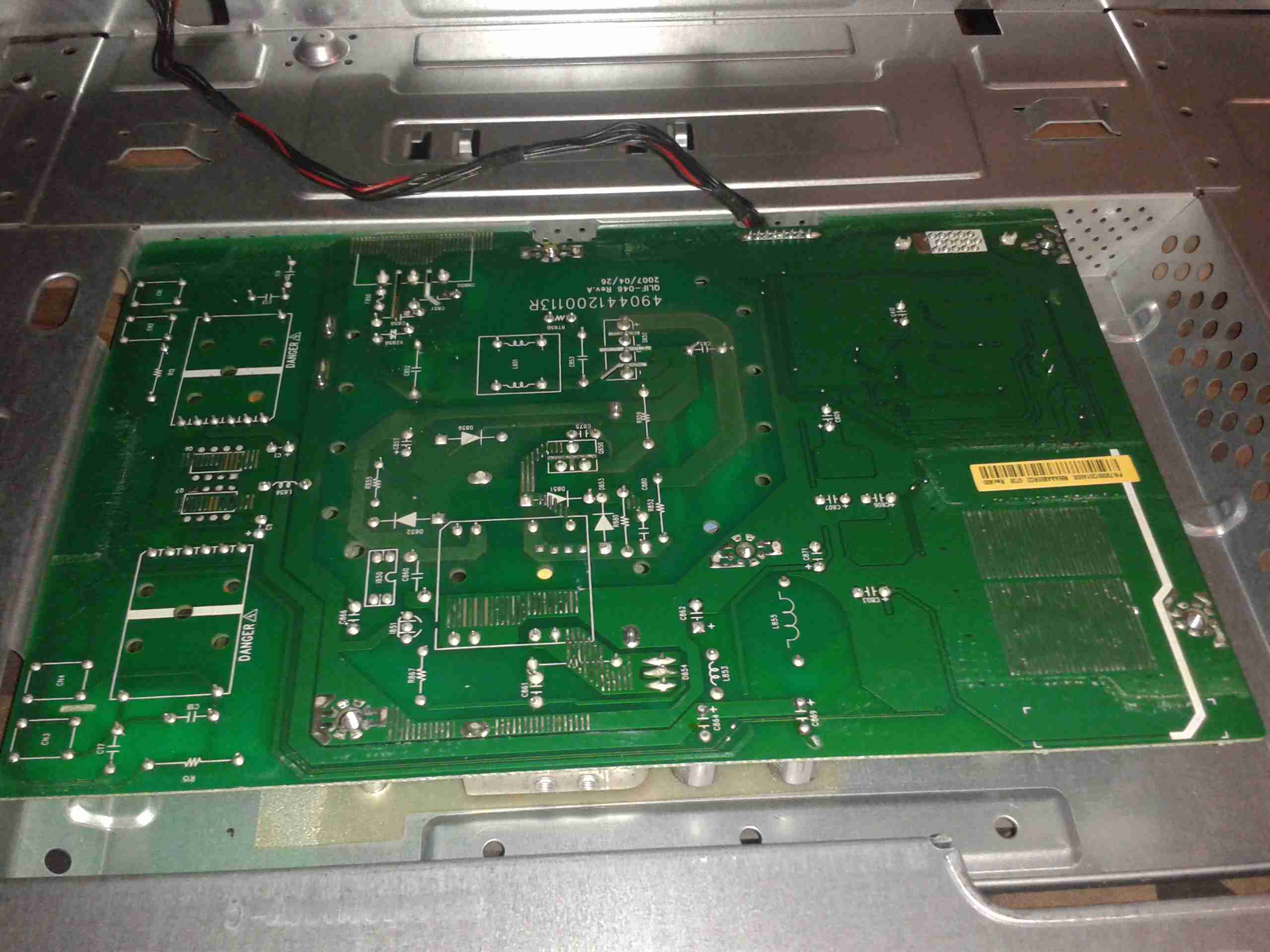
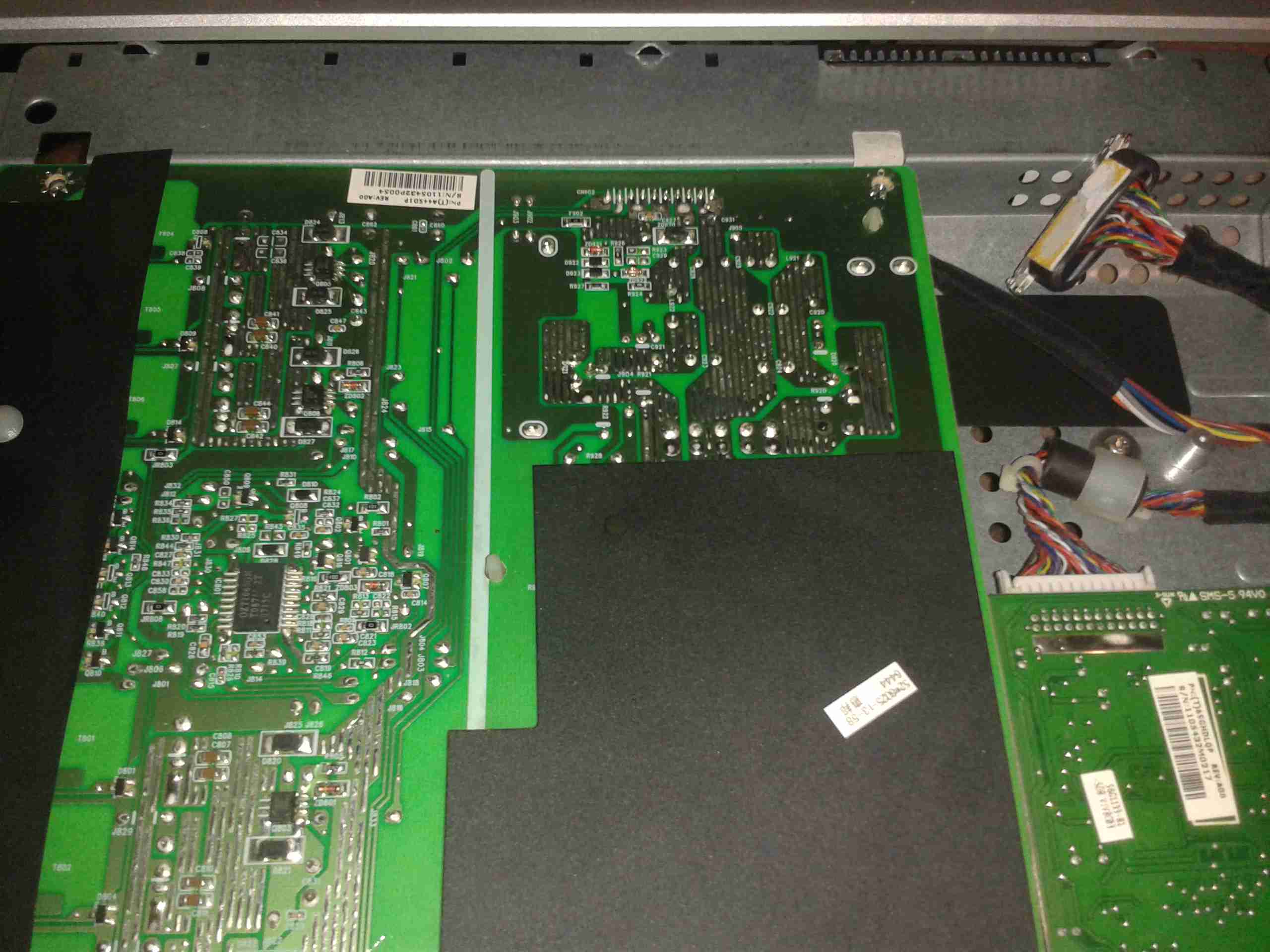
Main PCB
In this monitor type, there is only a single board, with all the PSU & logic, instead of separate boards for each function.
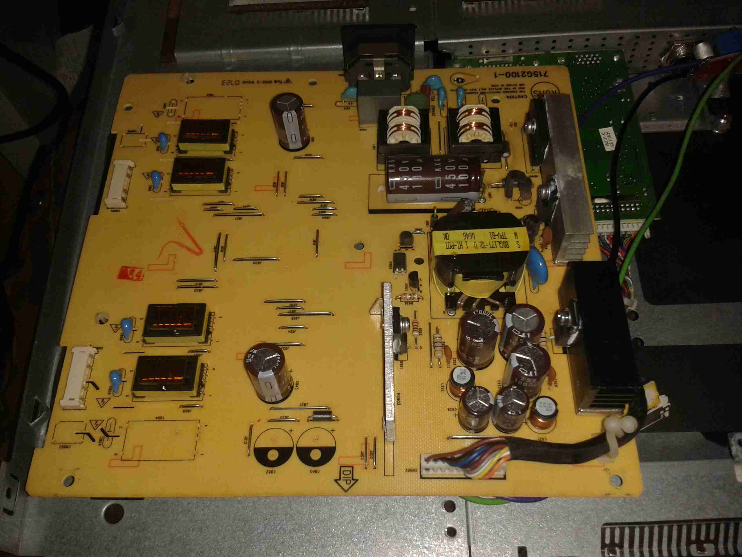
PSU Closeup
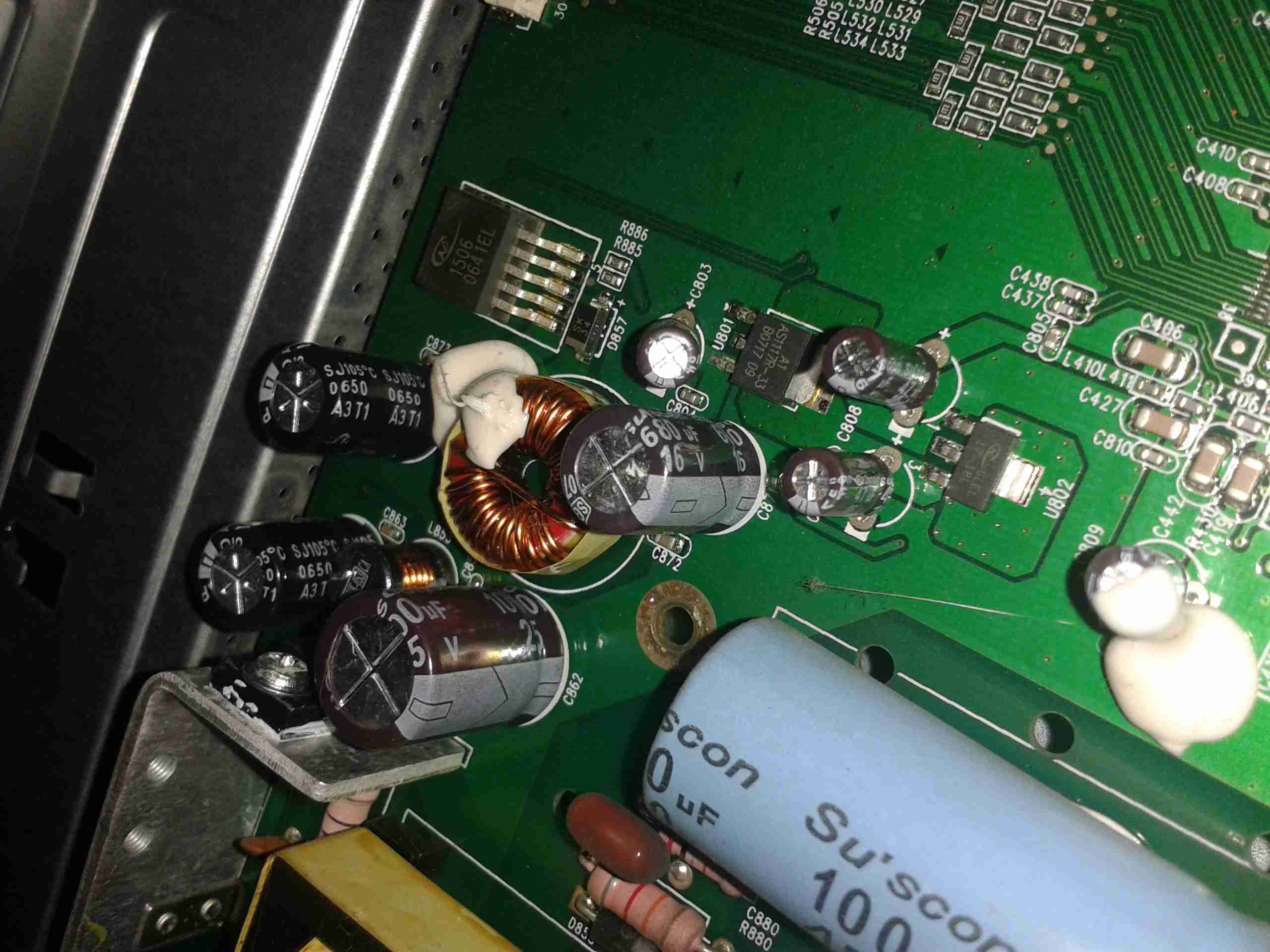
This monitor is slightly different in it’s power supply layout. The mains supply provides only a single 12v rail, which is then stepped down by a switching converter to 5v, then by smaller linear regulators to 3.3v & 1.8v for the logic. This makes my life easier since I don’t have to worry about any power conversion at all.
PCB Reverse
Here’s the backside of the PCB, the mains PSU section is in the centre.
Attachment Points
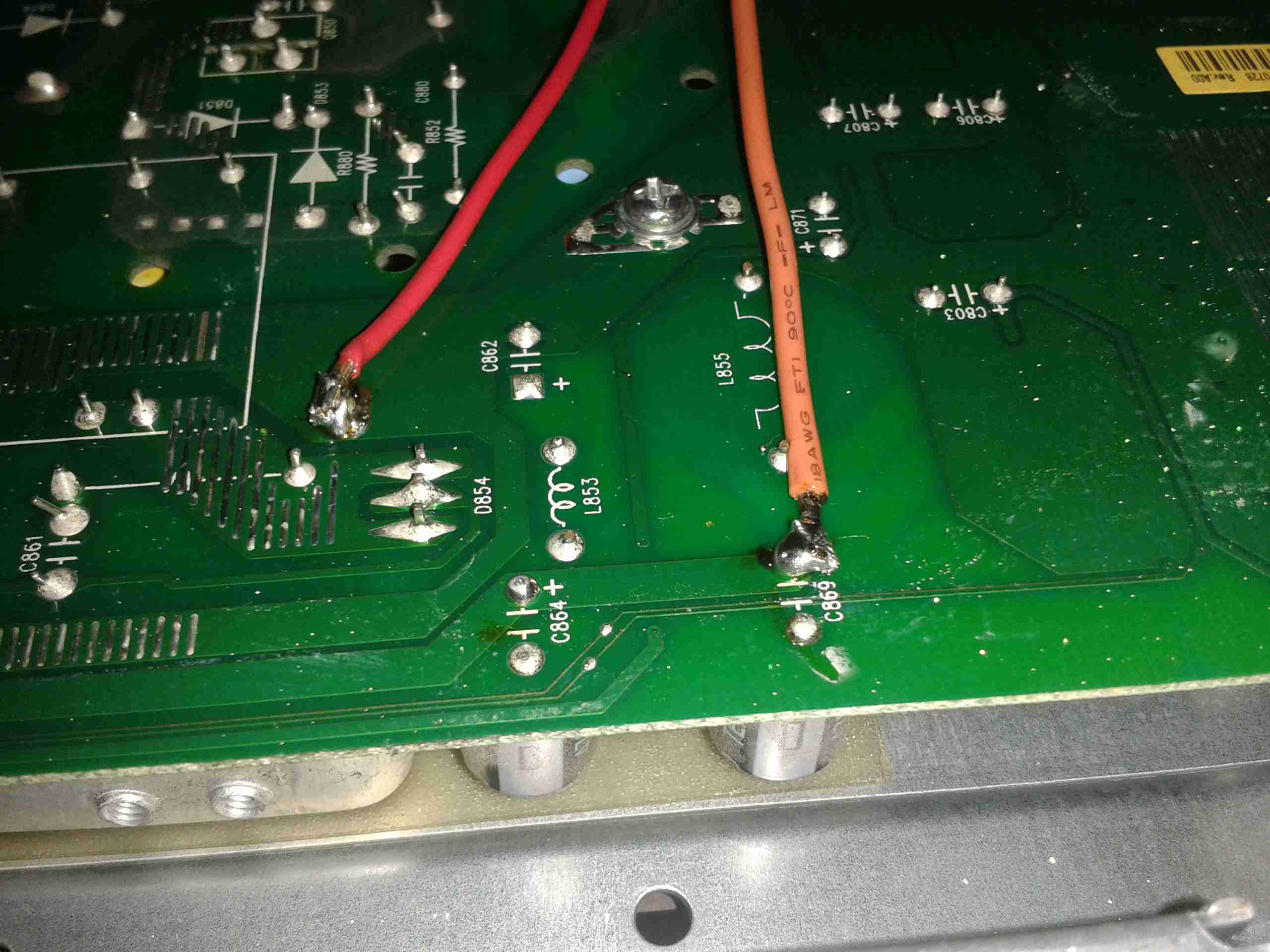
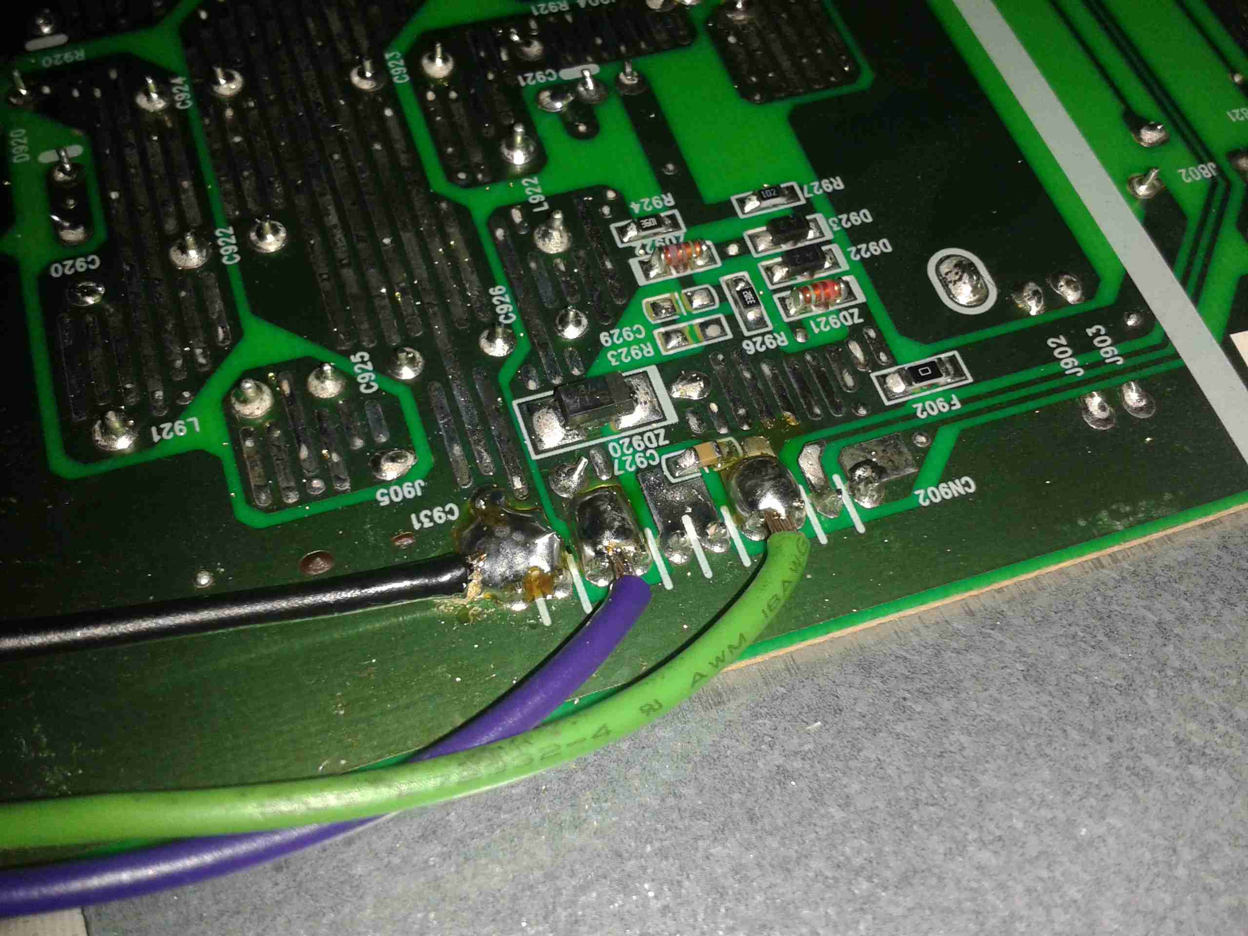
Here’s the pair of 12v supply wires soldered onto the main board, onto the common GND connection on the left, and the main +12v rail on the right. I’ve not bothered with colour coding the wiring here, just used whatever I had to hand that was heavy enough to cope with a couple amps.
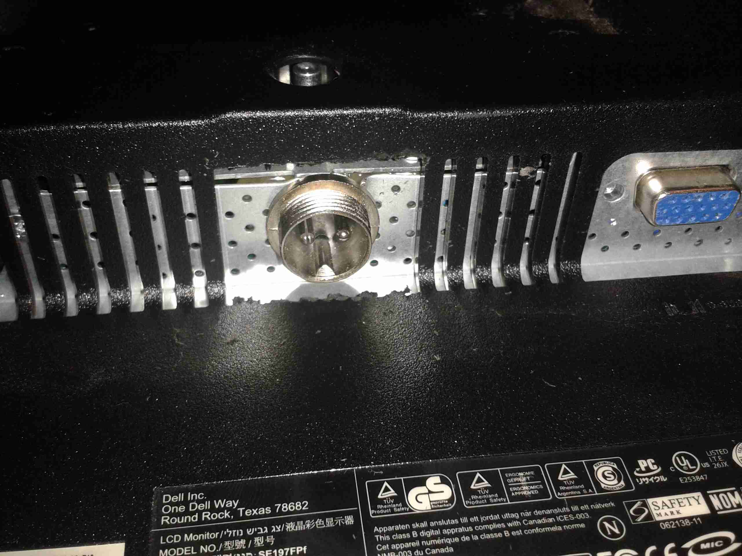
12v Socket
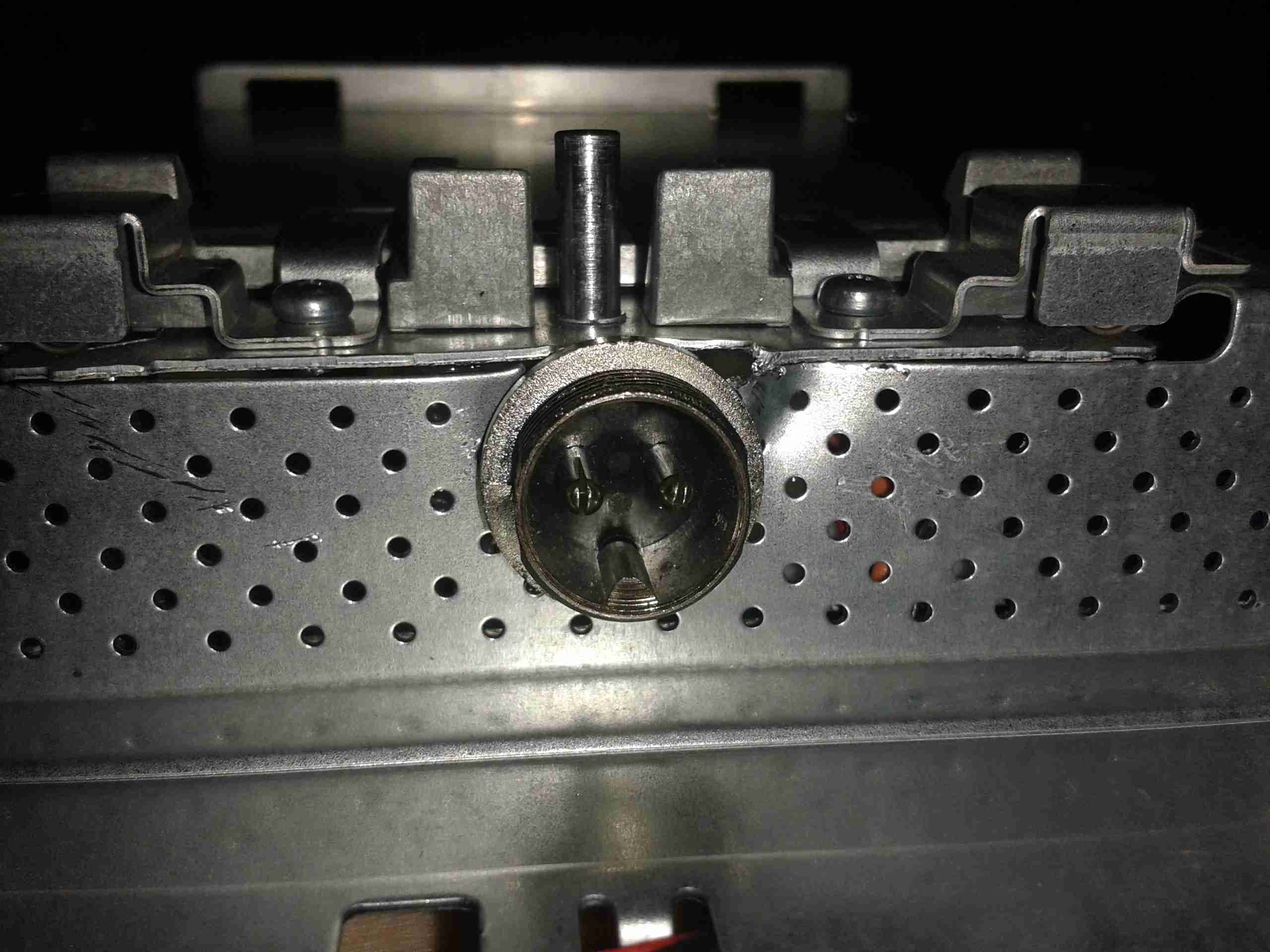
A small mod later with a cone drill & the 12v input socket is mounted in the LCD frame.
Casing Mod
Some light removal of plastic & the back cover fits back on. Current draw at 13.8v is ~2A.
I’m still on my crusade of removing every trace of 240v mains power from my shack, so next up are my computer monitors.
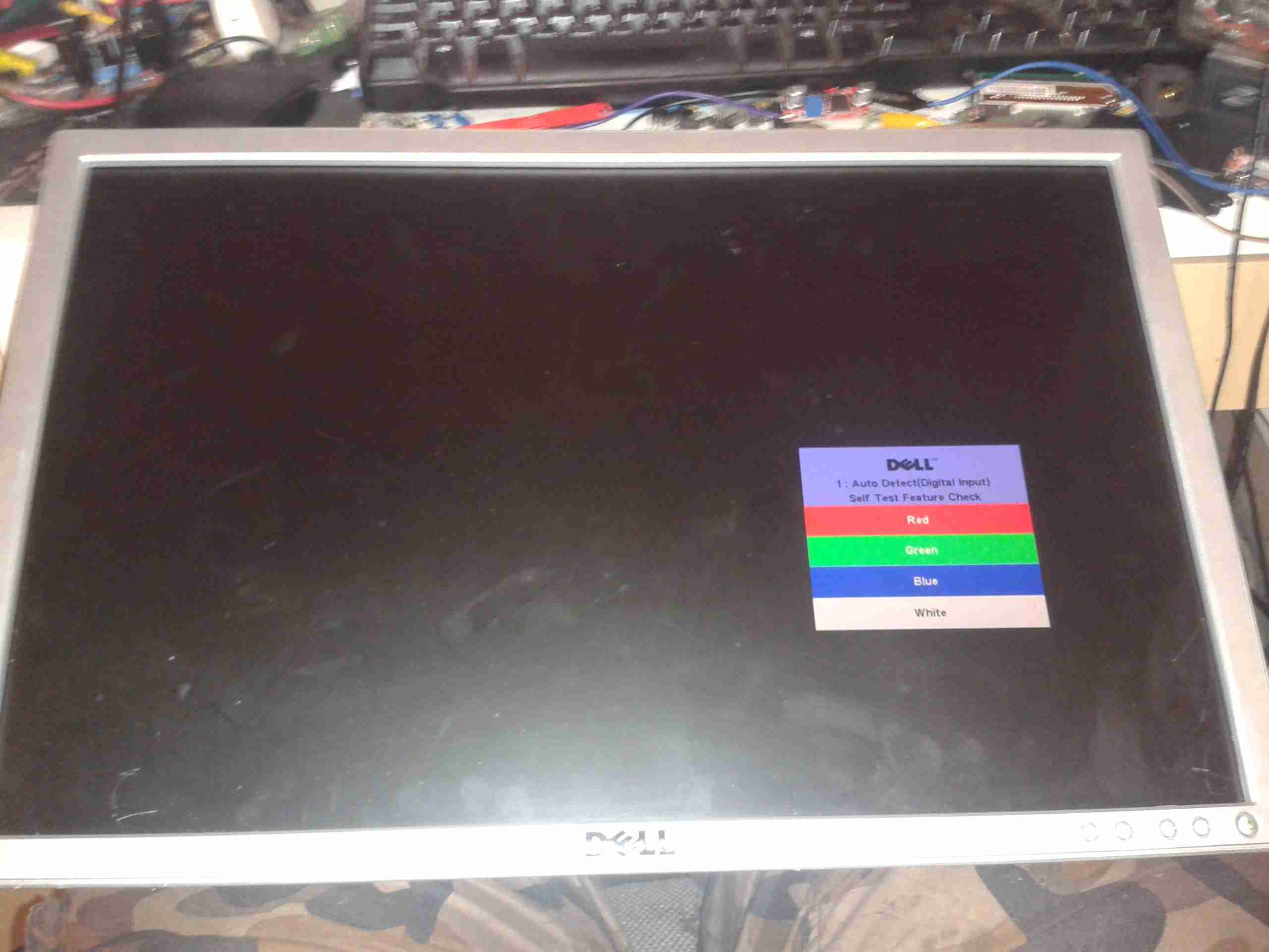
I have 4 Dell monitors, of various models, hooked up to my main PC.
The monitor here is a Dell E207WFPc 20″ widescreen model. There will be more when I manage to get the others apart to do the conversion. However I’m hoping that the PSU boards are mostly the same.
Panel Removed
There are no screws holding these monitors together, the front bezel is simply clicked into place in the back casing, these clips are the only thing that holds the relatively heavy glass LCD panel & it’s supporting frame! The image above shows the panel removed. The large board on the left is the power supply & backlight inverter, the smaller one on the right is the interface board to convert the DVI or VGA to LVDS for the LCD panel itself.
PSU Board
Here’s a closeup of the PSU board, the connector at centre right at the top of the PCB is the main power output, and also has a couple of signals to control the backlight inverter section of the PSU, on the left side. The PSU requirements for this monitor are relatively simple, at 14.5v for the backlight & 5v for the logic board.
PSU
Here’s the top of the PSU board, very simple with the mains supply on the right side, and the backlight inverter transformers on the left.
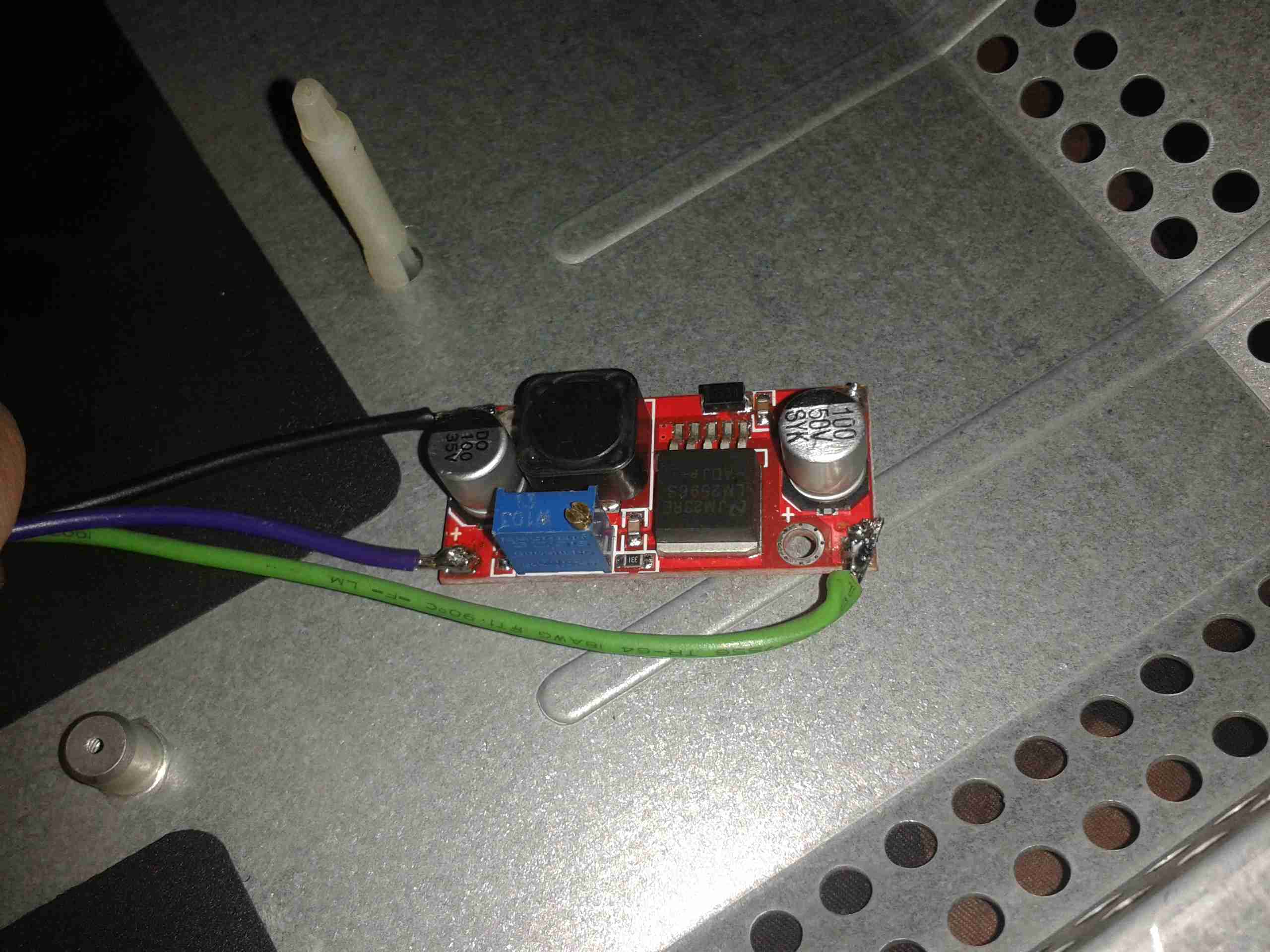
Hooked In
Here I’ve hooked into the power rails on the supply, to attach my own 12v regulators. The green wire is +14.5v, and the purple is +5v. Black is common ground.
5v Regulator
On doing some testing, the backlight inverter section doesn’t seem to mind voltages between 11.5-14.5v, so a separate regulator isn’t required there. Even running off batteries that’s within the range of both charging & discharging. The only regulator required is a 5v one to reduce the input voltage for the logic PCB.
First Test
On applying some 12v power to the regulator input, we have light! Current draw at 12.5v is 2.65A for a power consumption of 33W.
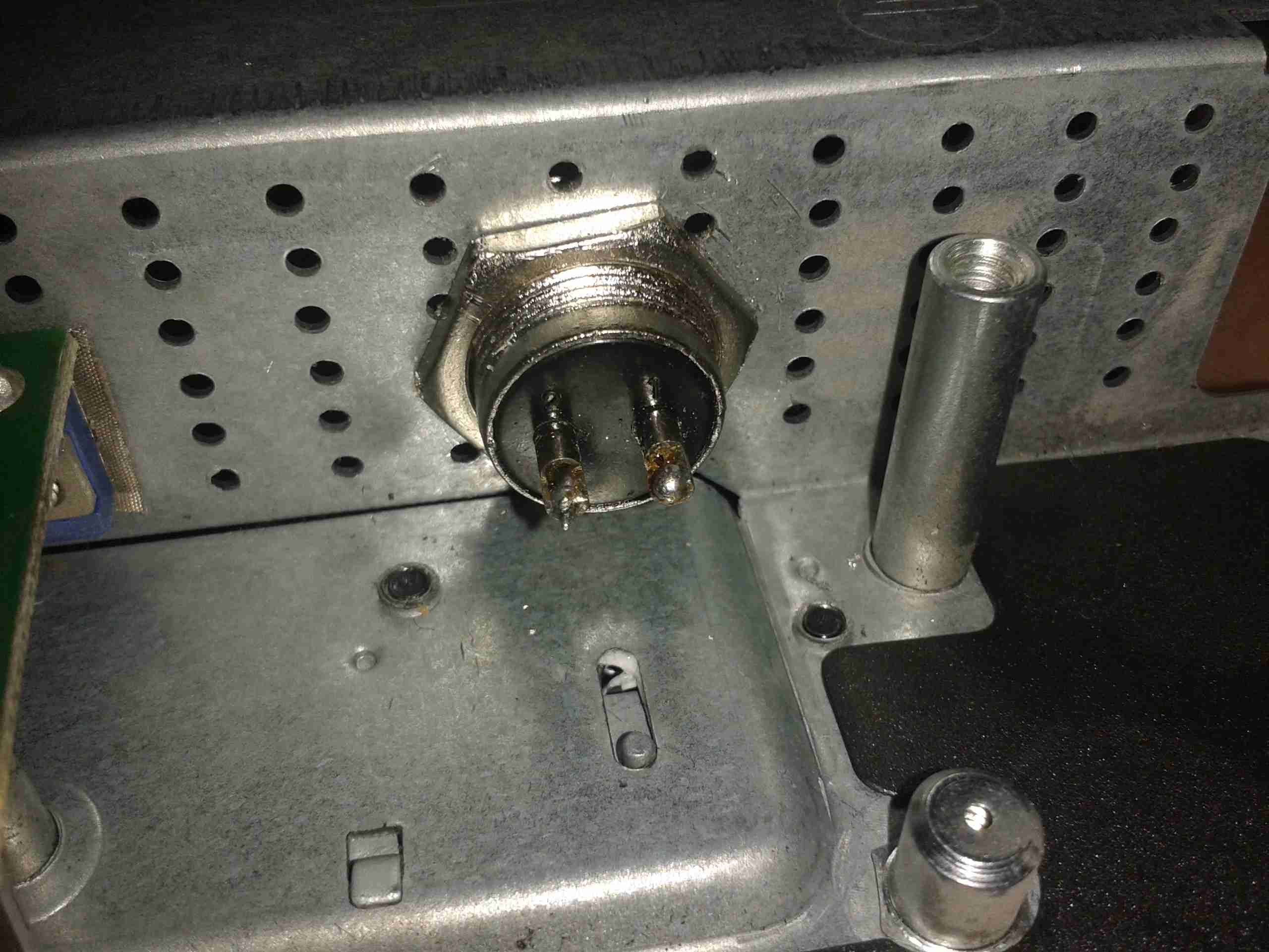
12v Input
There’s plenty of room in the back casing to mount a 12v input socket, I have left the mains supply intact so it can be used on dual supply.
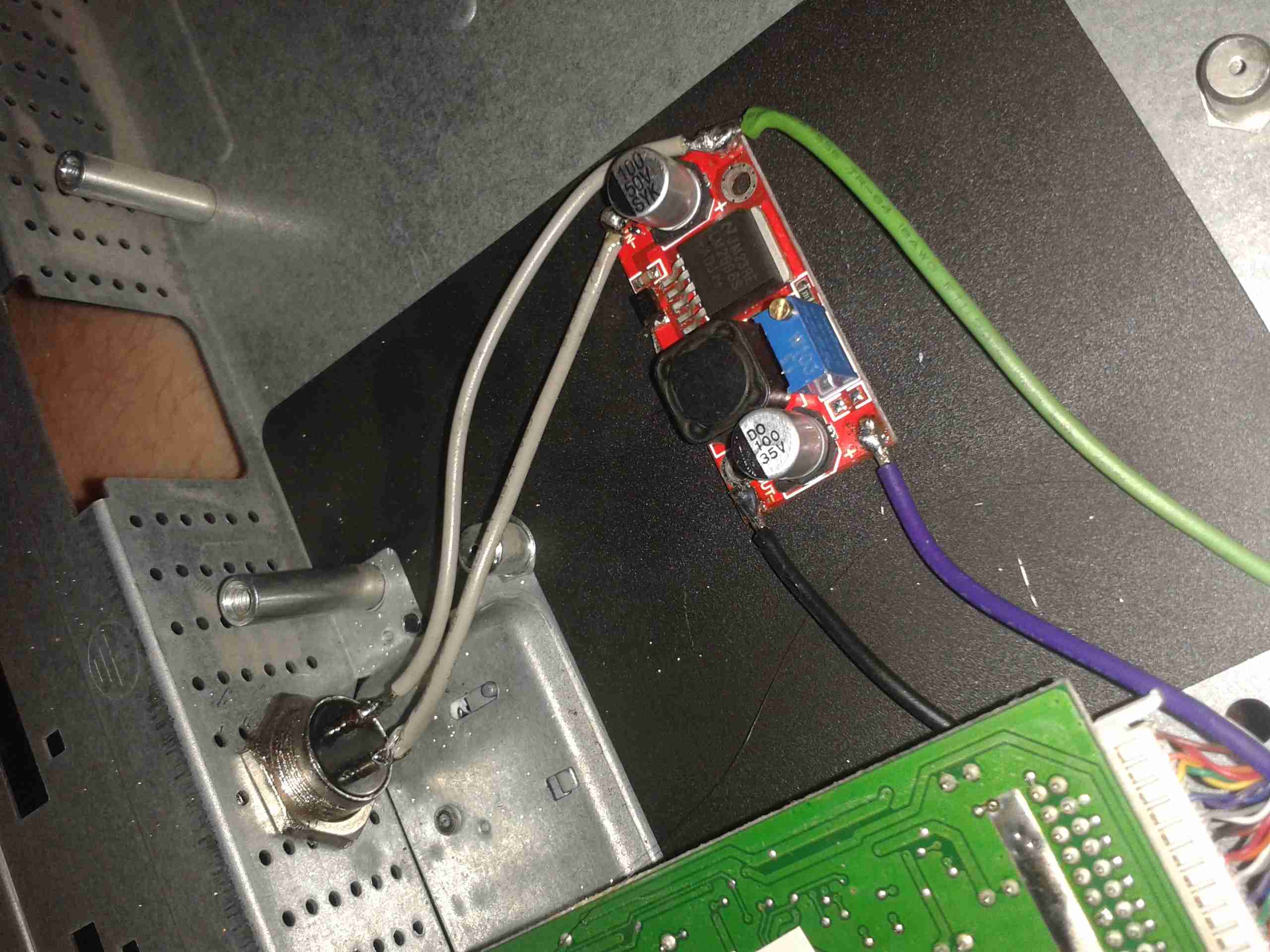
Final Wiring
Here’s the 5v regulator mounted on the back of the casing, all wired up & ready to go.
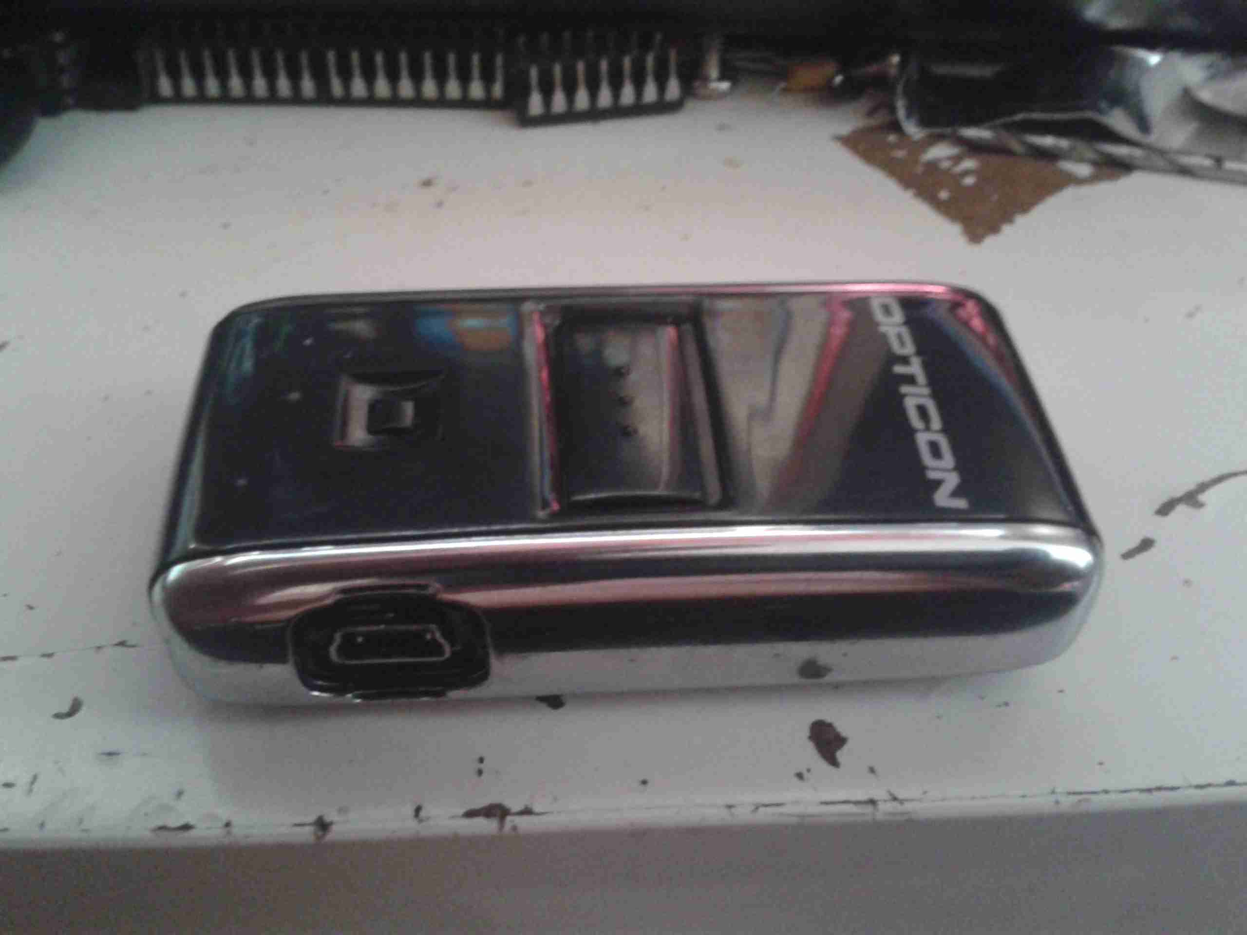
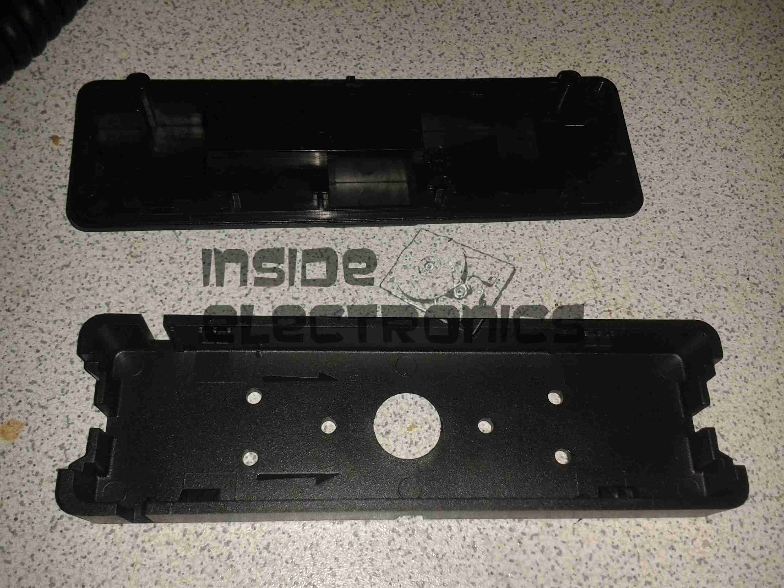
The OPN-2001 is a very small handheld barcode data collection device, used for stock keeping, inventory, etc.
It’s powered by an internal Li-Poly cell, at 150mAh, and has storage for 1000 barcodes in it’s internal memory.
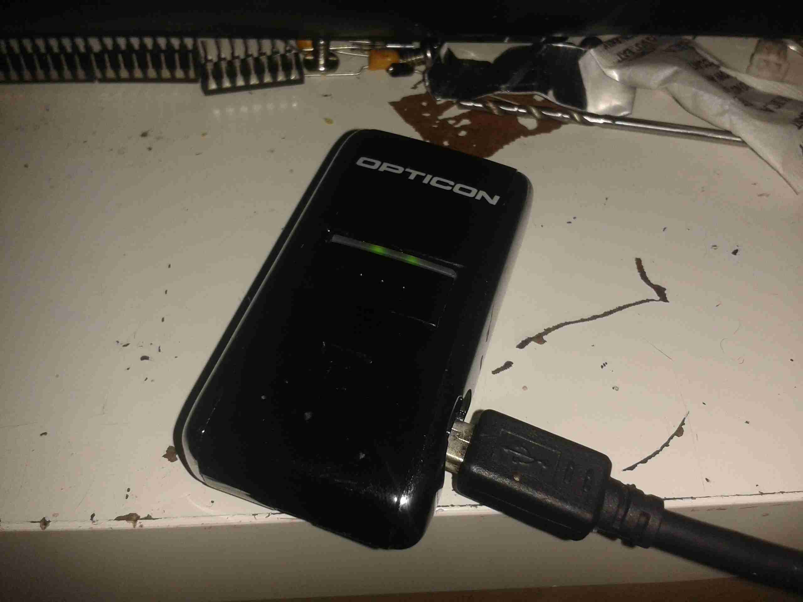
USB
The unit is charged via it’s USB port, the data can also be downloaded using this interface.
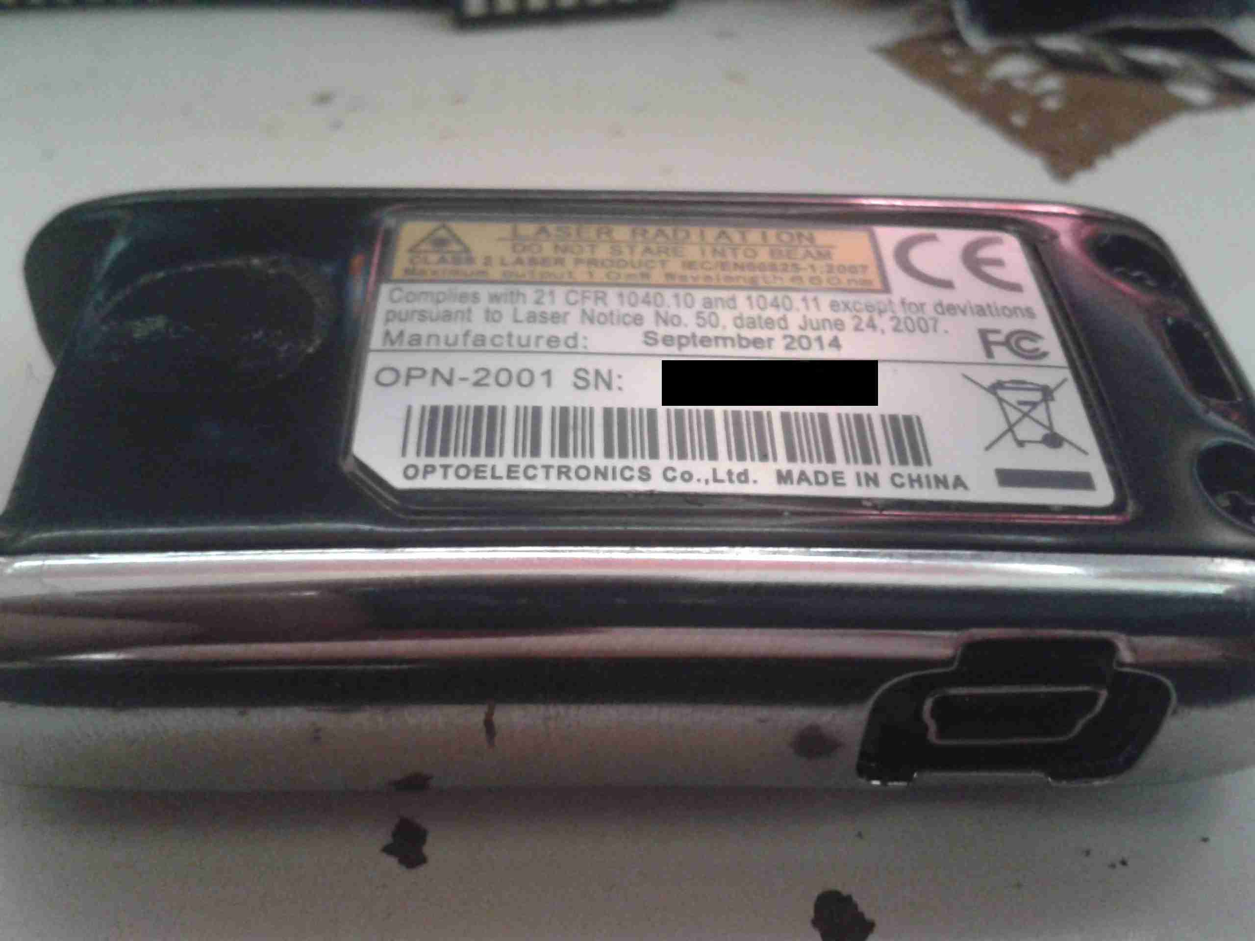
ID Label
Here’s the bottom of the unit with it’s label. Serial number removed to protect the guilty. 😉
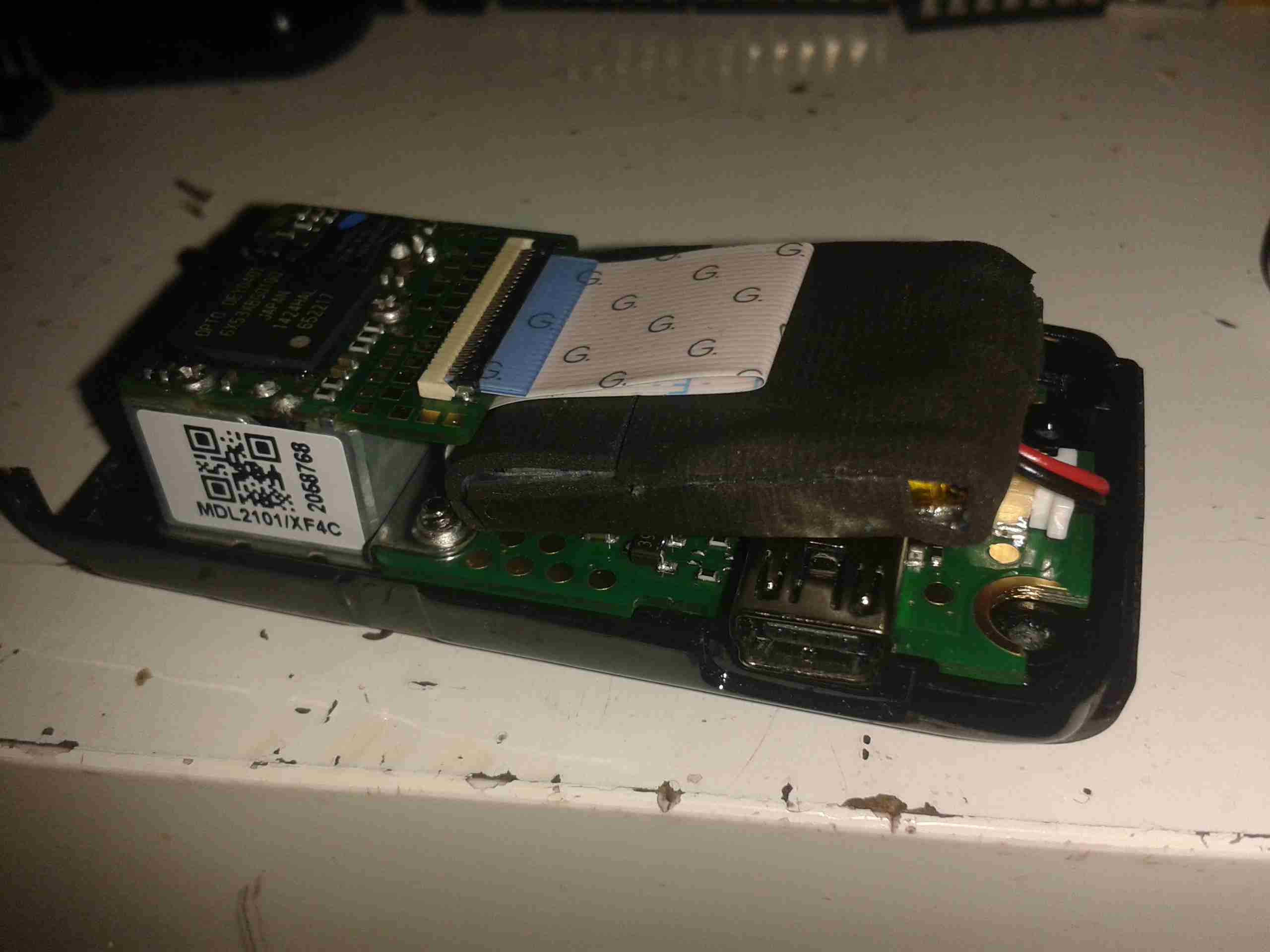
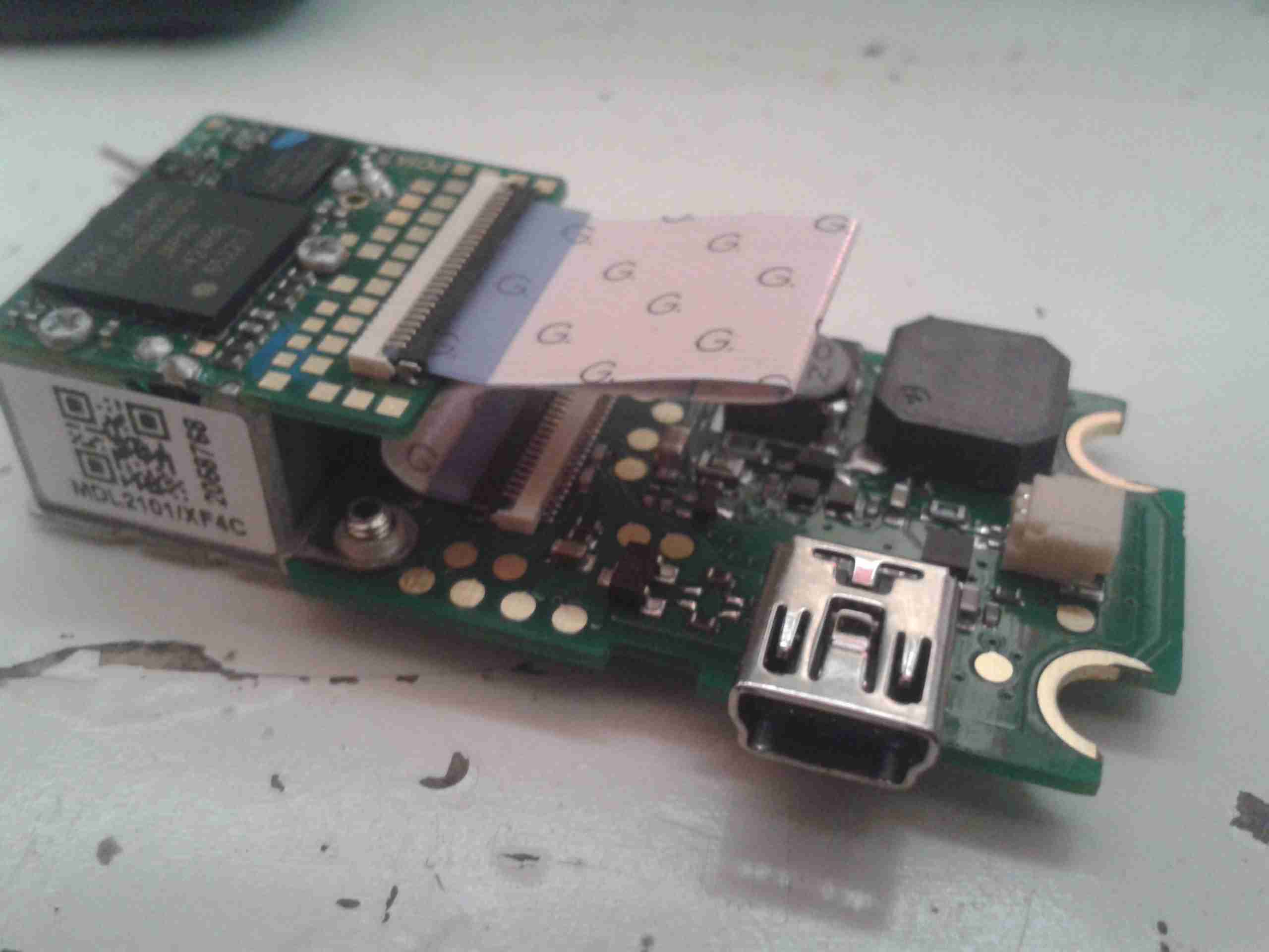
Cover Removed
Here the bottom cover has been removed from the scanner, showing the internals. The barcode engine is on the left, this contains all the hardware & logic for scanning & storing the barcode data. The Li-Poly cell is under the FFC cable wrapped in foam tape for protection.
PCB Removed
Here’s the PCB & engine assembly removed from the casing. The lower PCB appears to just handle the user interface buttons, beeper & USB power & charging circuitry. All the processing logic is on the barcode engine itself.
PCB Reverse
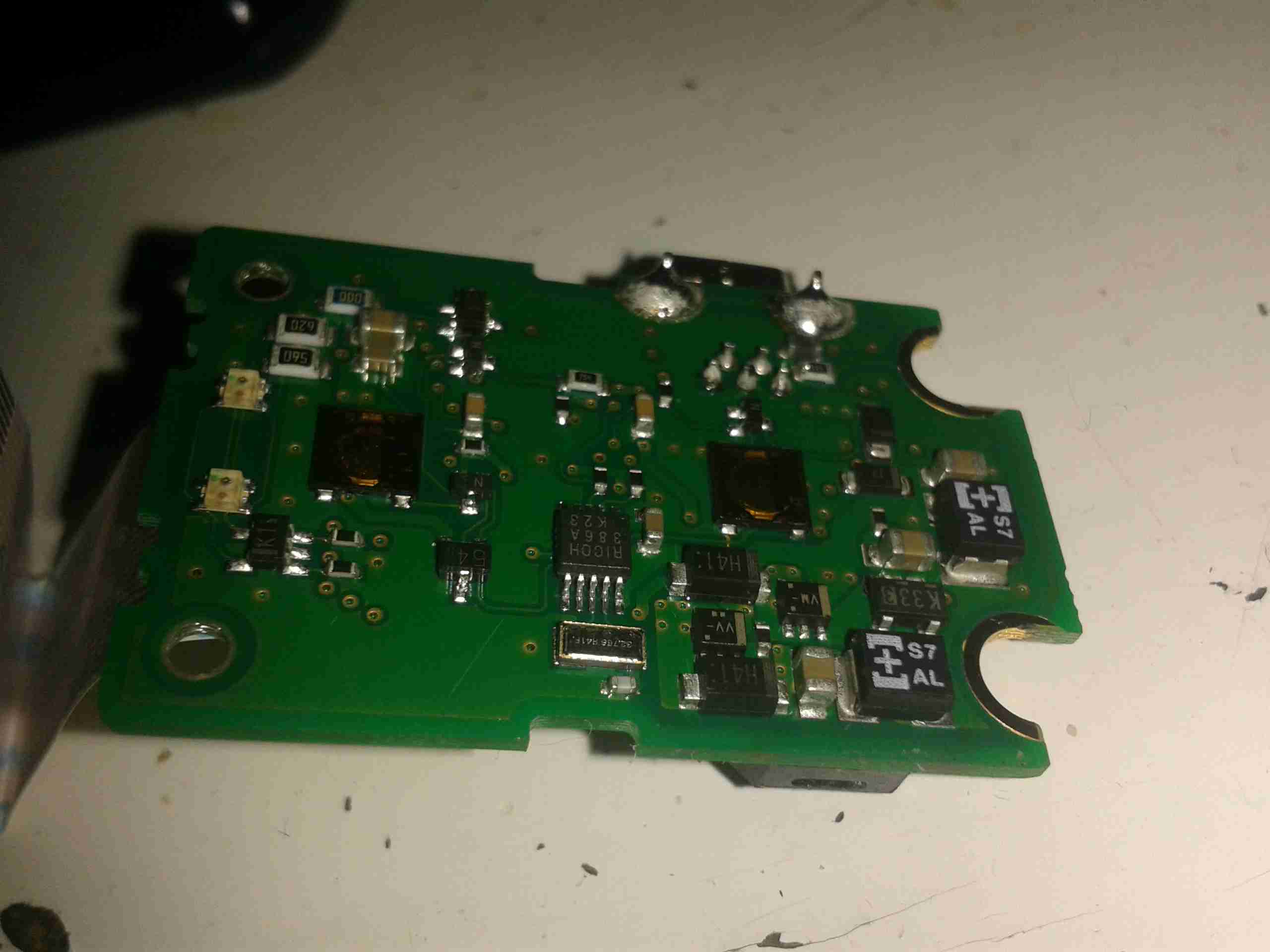
Here’s the back of the support PCB, with the pair of buttons for scanning & deleting barcodes. Also on this board is a 32kHz clock crystal & a Ricoh RV5C386A RTC IC. This communicates with the main processor via I²C for storing the date & time with the barcodes. At the bottom right corner are some of the power supply passives.
Support PCB
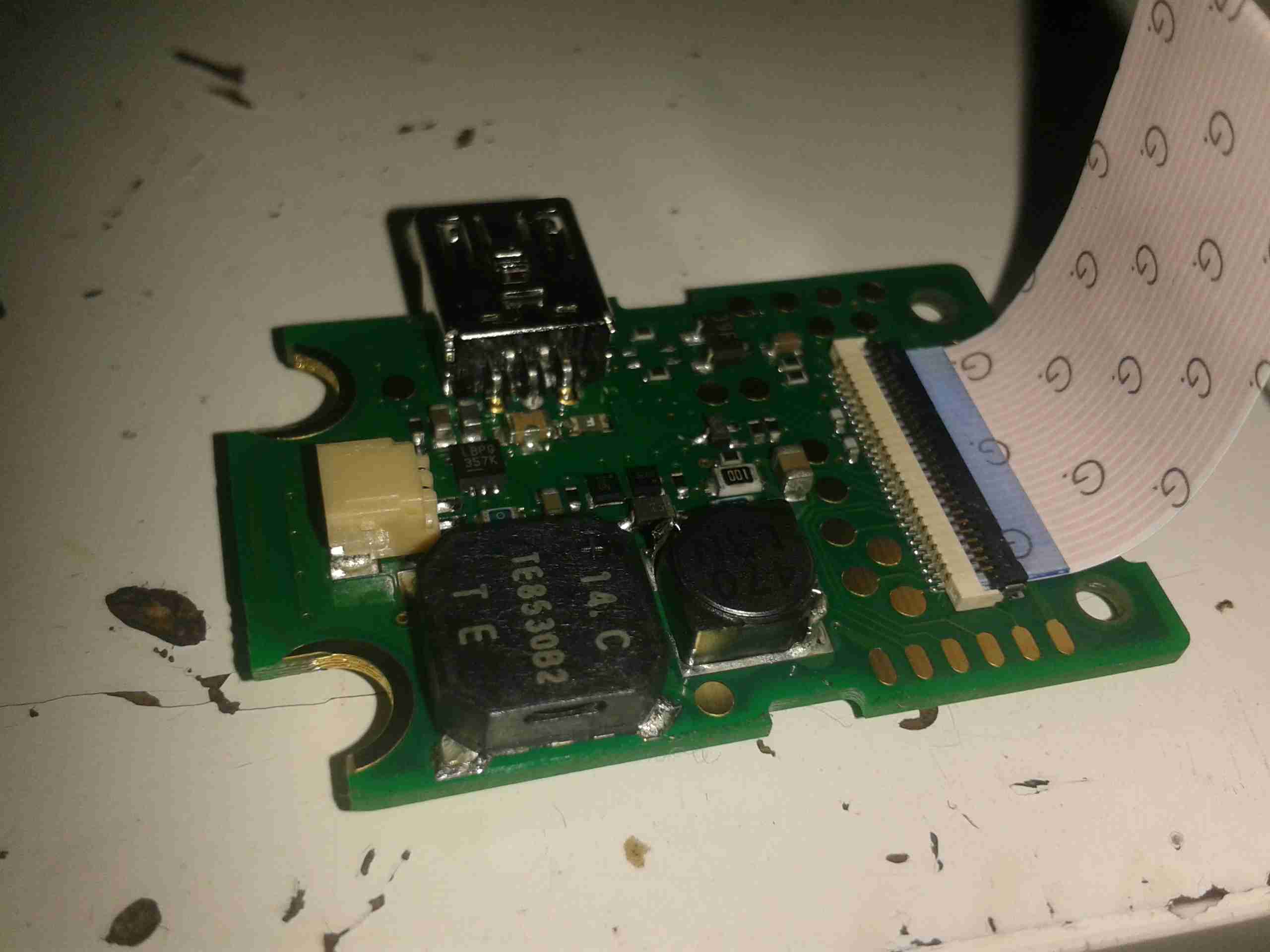
Here’s the other side of the support PCB, with the beeper, battery connector & the switching regulator to provide the barcode engine with 3.3v power.
Barcode Engine
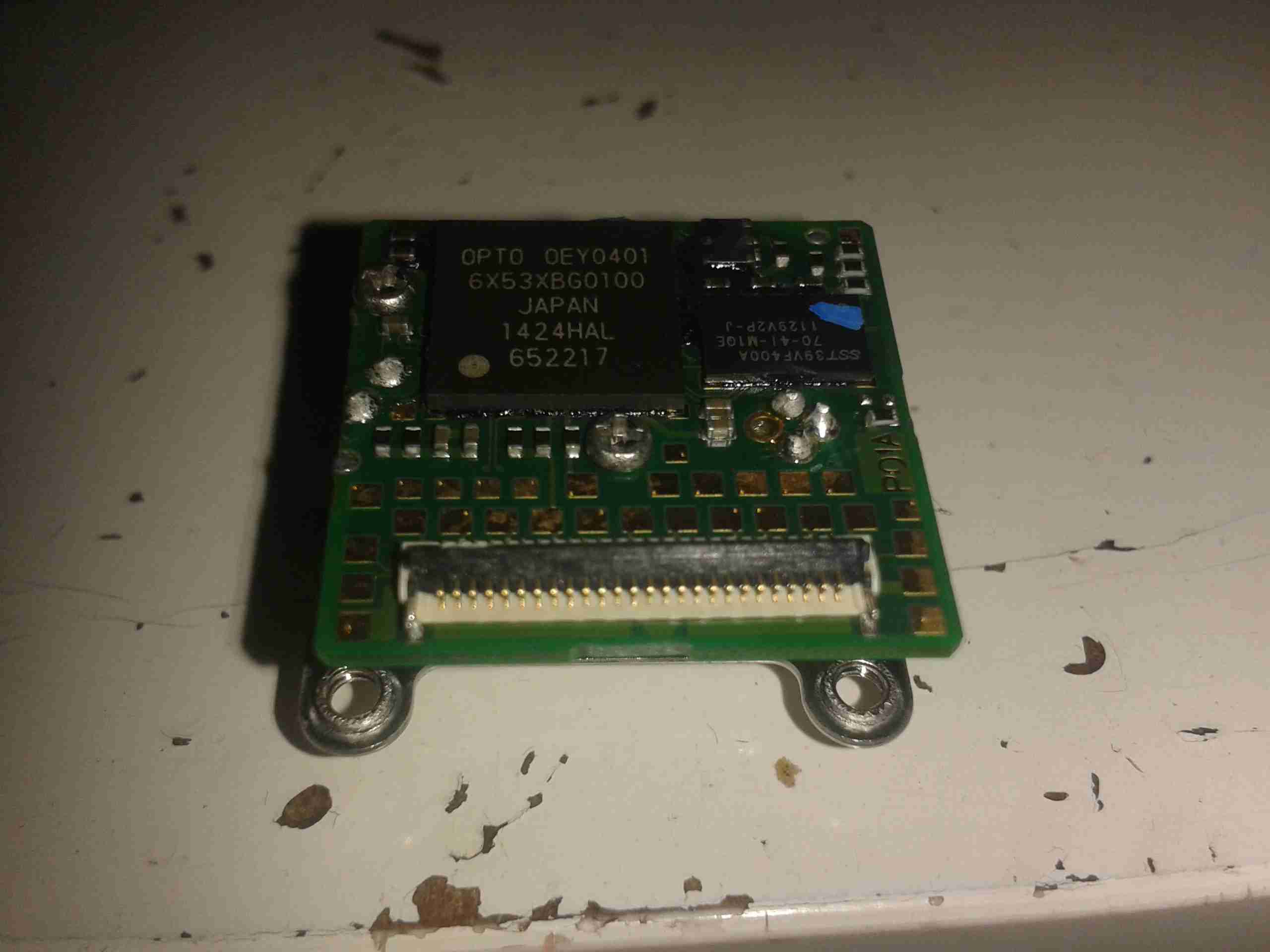
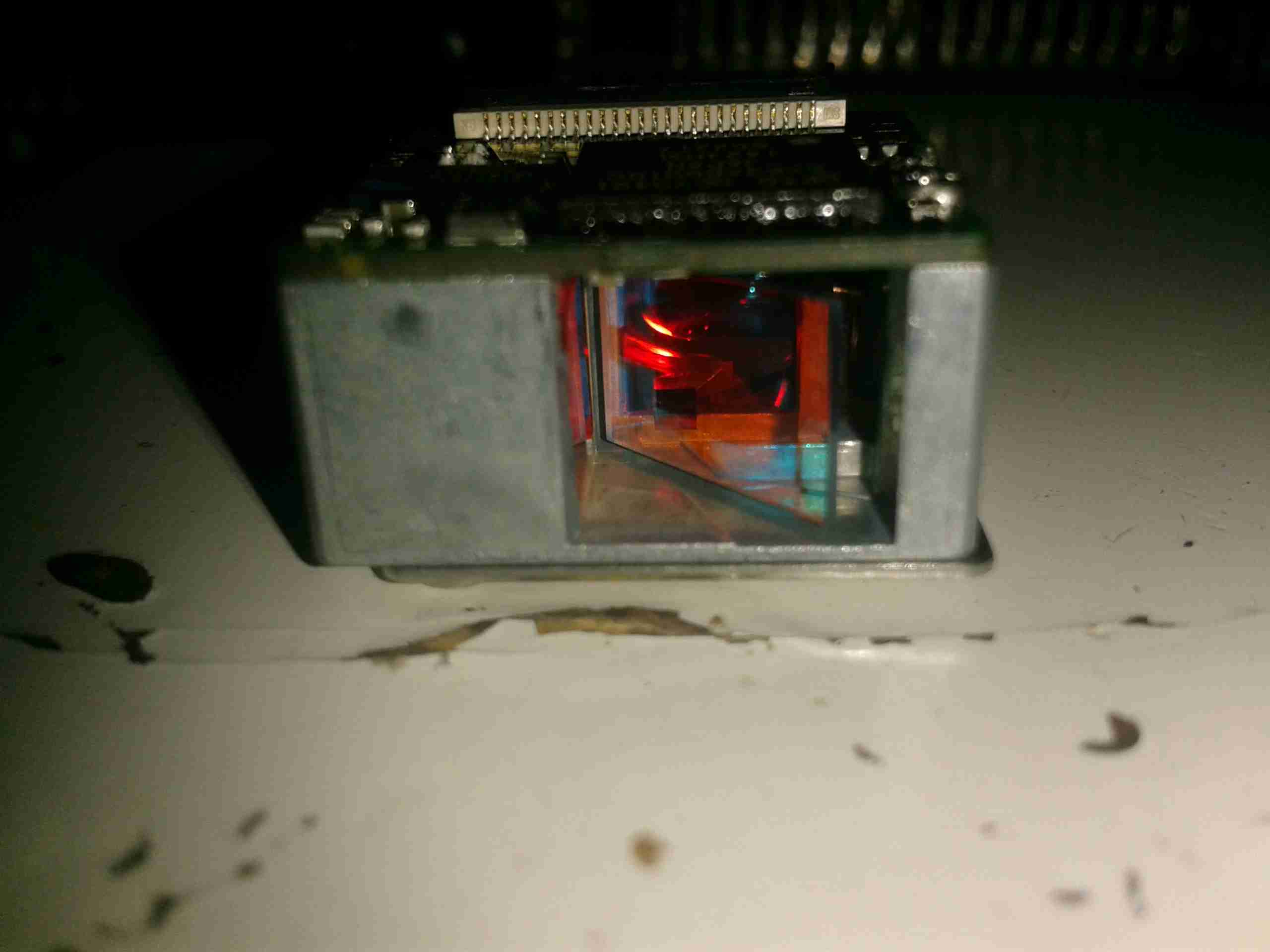
Here’s the barcode engine itself, which is absolutely tiny, at roughly 20mm square. The main processor & it’s associated Flash ROM are on this PCB. The main processor has an ARM7 32bit core, with 64kB of RAM, and onboard 512kB of ROM for program & barcode storage.
Mirror
Here’s the business end of the barcode engine, the mirror vibrates at 100Hz to produce the scan line. The laser diode is rated at 1mW, 650nm. This is in the deep red range.
All of the parts I required to complete the supply arrived this morning. After several hours of building, here’s what I came up with:
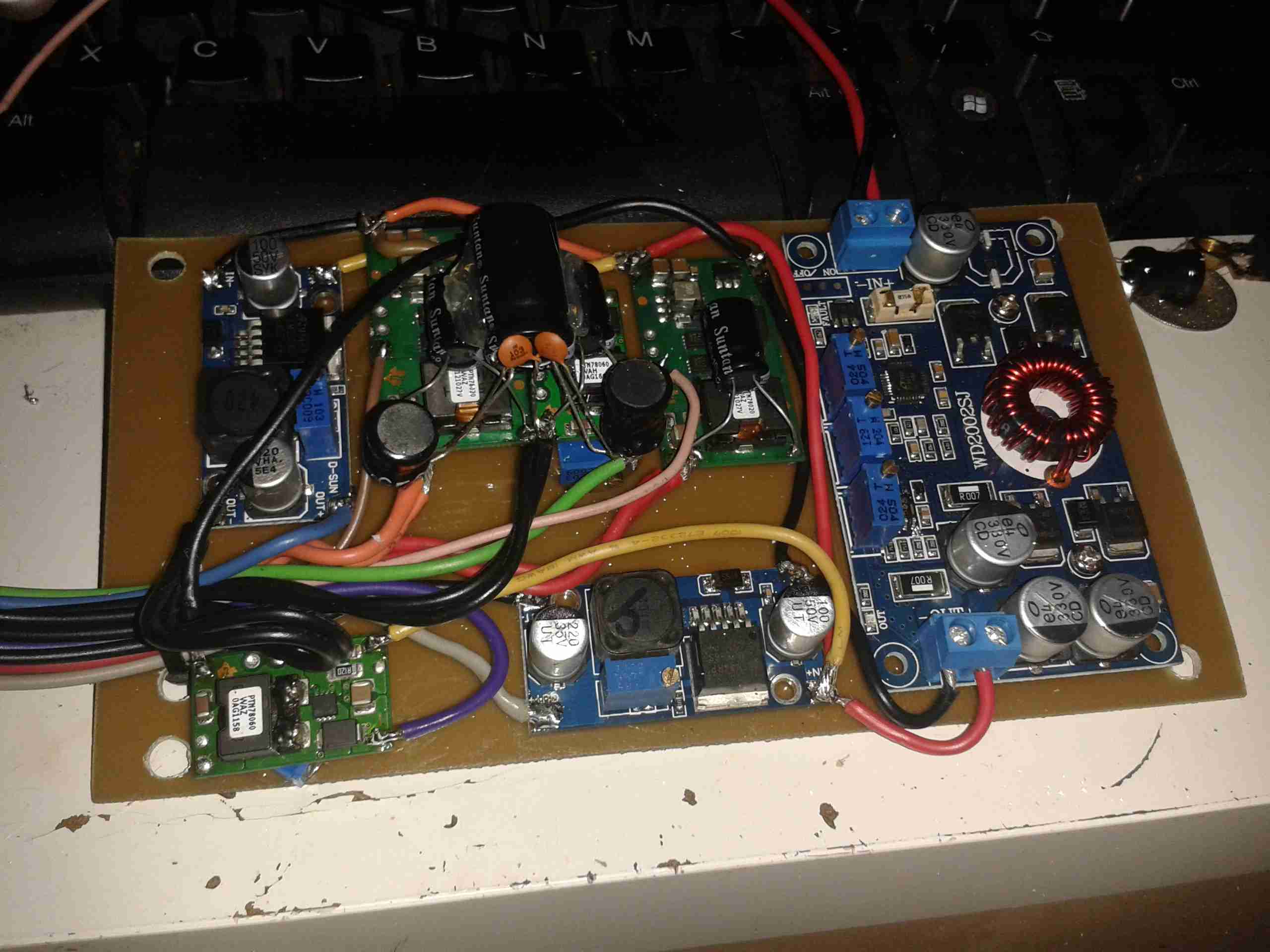
12v Power Supply
I’ve mounted everything on a piece of FR4 PCB, with it’s copper plane grounded to the case. This backing board is the same size as the original PSU PCB to allow it to be screwed into the same location in the scope.
The power comes in via the converter on the right, which outputs a single 24v rail for the rest of the supplies. The other 6 supplies then generate the individual voltage rails that the scope requires. The use of a single input supply allows this system to operate at voltages up to 30v DC, so it’s good for both 12v & 24v systems.
Scope Ripple
At present the only issue is with some ripple on one of the supplies, this is showing up on the scope display with no input connected at the lowest volts/division. Parts are on order from Farnell to build some common mode filters to remove this from the DC output.
On a 13.8v supply, the scope draws about 1.5A total from the supply, giving a total power consumption of 20.7W. This is with all 4 channels enabled.
My wiring assignments & DC-DC converter ratings are in the table below
Connector Pin
PCB Pin
Signal
Mainboard
DC-DC Rating
Wire Colour
1
10
GND
GND
N/A
BLACK
2
2
+9v_GND
FAN --
NA
BLACK
3
8
+7.5V
6.3V
6A
ORANGE
4
14
-7.5V
-7.5V
2A
GREEN
5
1
NOT USED
AC_TRIG
N/A
NOT USED
6
4
+5V
5V5A
6A
RED
7
6
GND
GND
N/A
BLACK
8
7
GND
GND
N/A
BLACK
9
12
-17.5V
-17.5V
3A
PURPLE
10
9
+7.5V
6.3V
6A
ORANGE
11
3
+9V
FAN +
1A
GREY
12
11
17.5V
17.5V
3A
BLUE
13
5
+5V
5V5A
6A
RED
14
13
GND
GND
N/A
BLACK
Stay tuned for the final section of this build with the power supply filtering & main DC input connections!
Since everything in my shack is run from 12v, I thought it would be handy to convert my new scope to 12v as well, as 99% of the places I find myself needing test gear are off grid, with no access to mains supplies.
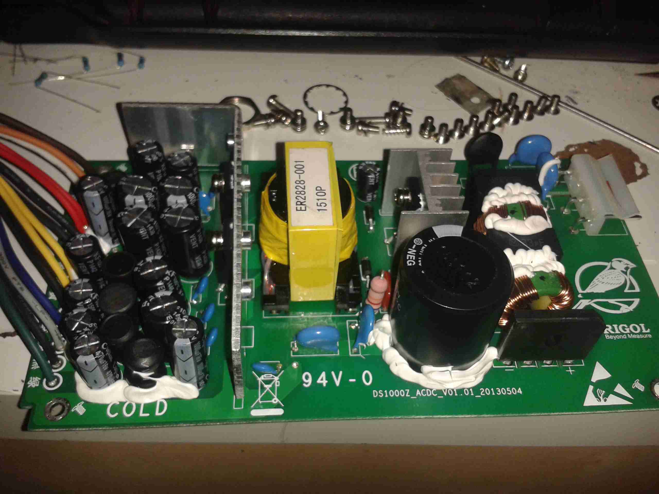
Mains PSU
Here’s the factory mains SMPS unit from the back of the scope. This is a nice multi-rail unit, with several different outputs, the table below details the wiring of the PSU.
Connector Pin
PCB Pin
Signal
Measured Voltage
Mainboard
Rectifier Rating
Wire Colour
5
1
AC_TRIG
N/A
AC_TRIG
N/A
BROWN
2
2
+9v_GND
N/A
FAN --
NA
ORANGE
11
3
+9V
10.16V
FAN +
2A
WHITE
6
4
+5V
5.1V
5V5A
20A
RED
13
5
+5V
5.1V
5V5A
20A
RED
7
6
GND
N/A
GND
N/A
BLACK
8
7
GND
N/A
GND
N/A
BLACK
3
8
+7.5V
6.9V
6.3V
20A
YELLOW
10
9
+7.5V
6.9V
6.3V
20A
YELLOW
1
10
GND
N/A
GND
N/A
BLACK
12
11
17.5V
17.51V
17.5V
2A
BLUE
9
12
-17.5V
-17.36V
-17.5V
2A
GREY
14
13
GND
N/A
GND
N/A
BLACK
4
14
-7.5V
-6.84V
-7.5V
2A
GREEN
The only feature I will lose if I make this switch is AC line triggering, but I never use that anyway, so it’s not a big issue for me.
Since I have been able to locate the connector, the plan is to design a replacement low voltage supply unit for the scope, with the same footprint as the original AC mains supply. This will allow me to do a direct swap without causing any damage or modifying the original supply.
This method will allow me to swap the 240v supply back into the scope if I ever come to need it.
I’m planning to use the LTC3863 DC-DC Controller from Linear Tech to generate the negative rails, this will go down to -150v on the output, so it’s pretty much perfect to generate them.
PSU Output Side
Here’s the output side of the mains PSU, it has a lot of filtering on the output rails, the two TO220 devices are the output rectifiers for the +5v & +7.5v rails, these are rated at 20A, 60V.
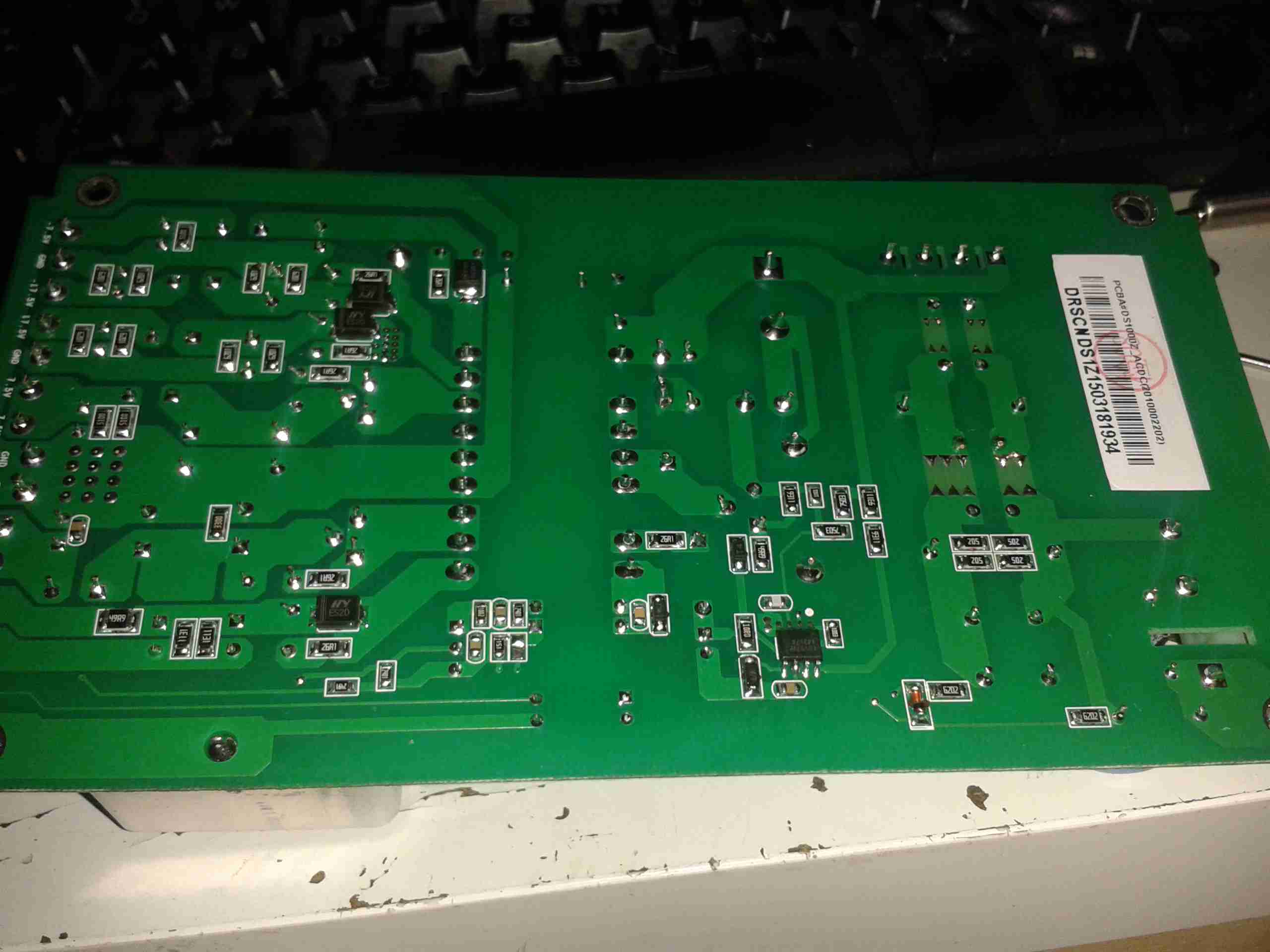
PCB Bottom
Here’s the bottom side of the PCB. It’s a really nicely designed PSU, massive isolation gap, spark gaps on the primary side & good filtering. The output side on the left has the rectifier diodes for the other voltage rails, these are only 2A rated, so designing the inverting supply to generate the negative rails will be pretty easy.
From looking at the PCB markings on both the mainboard & the PSU, the +9v rail seems to be used to drive the fan, both silkscreen markings indicate this.
The voltages marked on the PSU & the mainboard connector don’t quite match up though, there’s a small variation in the stated voltage between the two. This is most likely because all of the regulation of the supplies seems to be done on the mainboard, there are several linear regulators, and a few DC-DC switchers. Providing that the replacement supply isn’t noisy it should work fine.
This is backed up by the fact that the mains PSU only seems to regulate the +5v rail – on measuring the rails that’s the only one that’s close to spec.
Mainboard Power
Here’s the mainboard power connector, with it’s silkscreen labelling on the pins. (Very useful). As can be seen here, there’s at least 5 regulators, of both switching & linear types here, generating both positive & negative rails.
I recently dug out my other card printer to fit it with a 12v regulator, (it’s 24v at the moment), and figured I’d do a teardown post while I had the thing in bits.
This is a less industrial unit than my Zebra P330i, but unlike the Zebra, it has automatic duplexing, it doesn’t have Ethernet connectivity though.
Unlike domestic printers, which are built down to a price, these machines are very much built up to a spec, and feature some very high quality components.
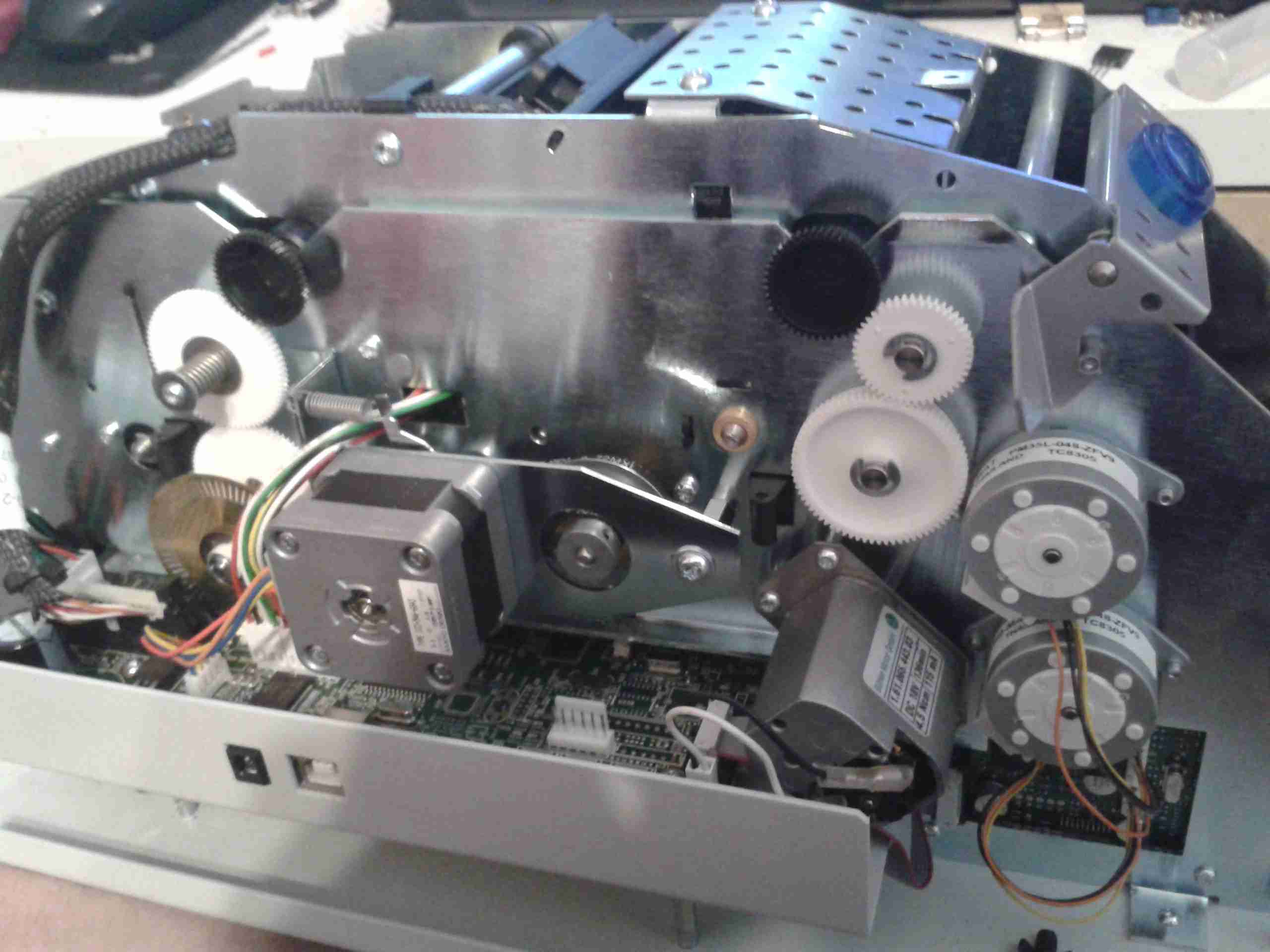
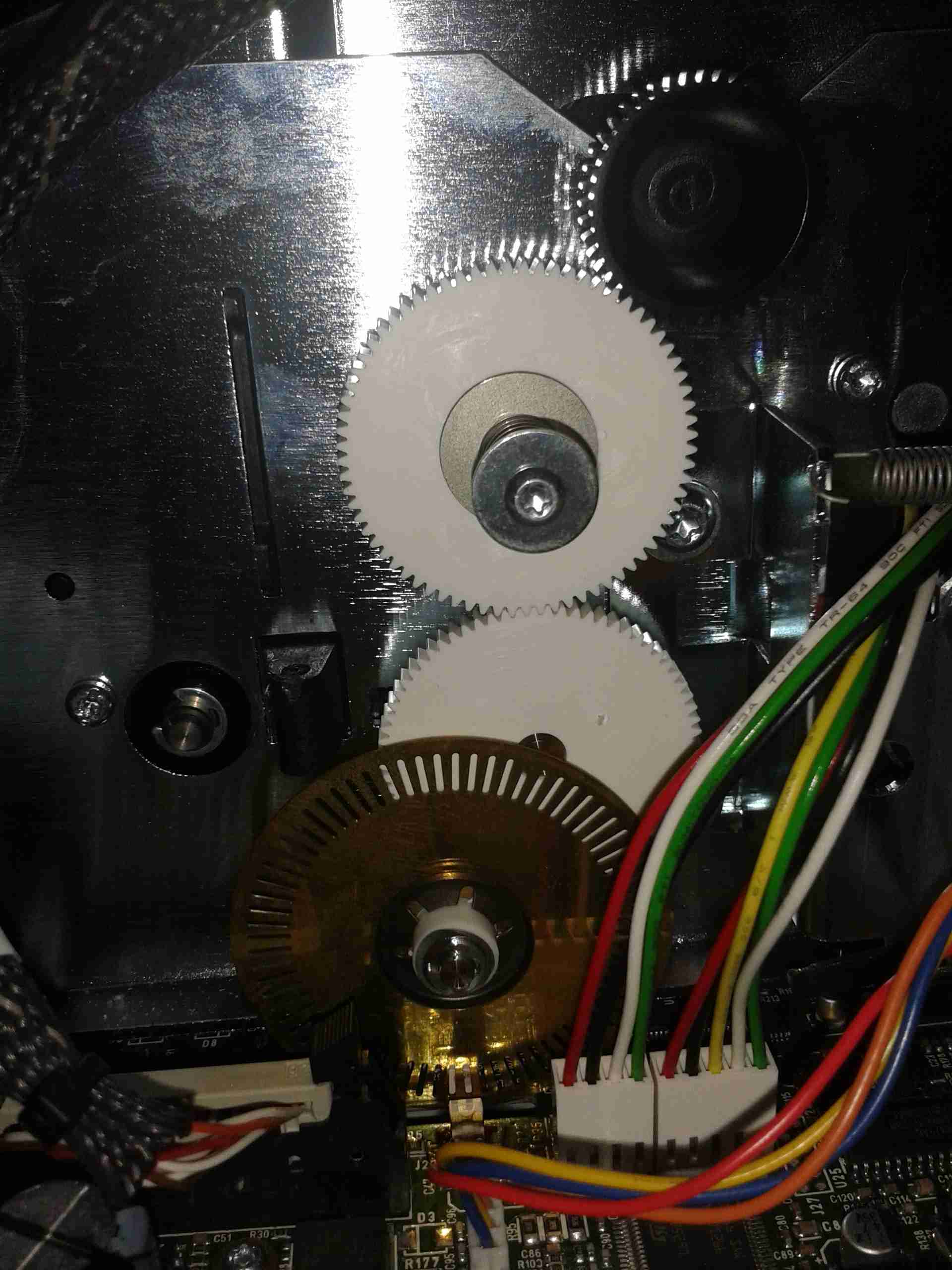
Naked Printer
Here’s the mechanism with the cowling removed. This is the main drive side of the printer, with the main drive stepper at left, ribbon take-up spool motor lower right, and the duplex module stepper motors at far right.
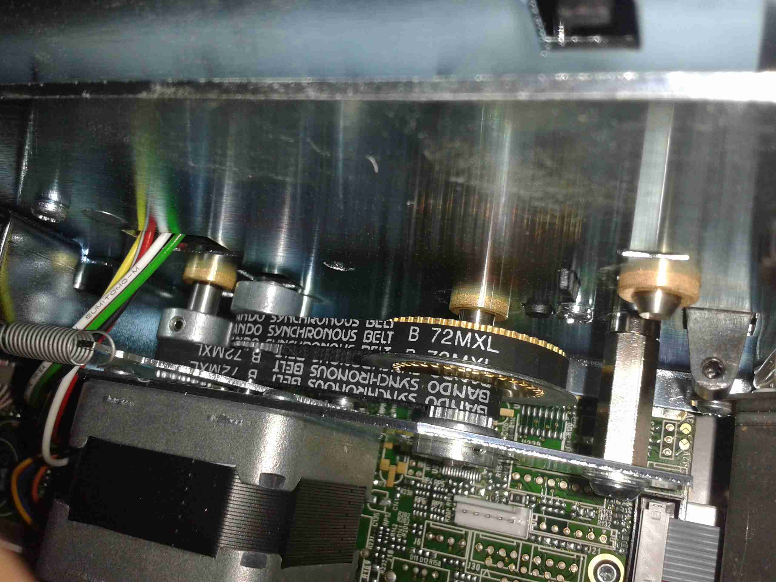
Main Motor Drive
The main drive motor runs the various rollers in the card path through a pair of synchronous belts, shown here.
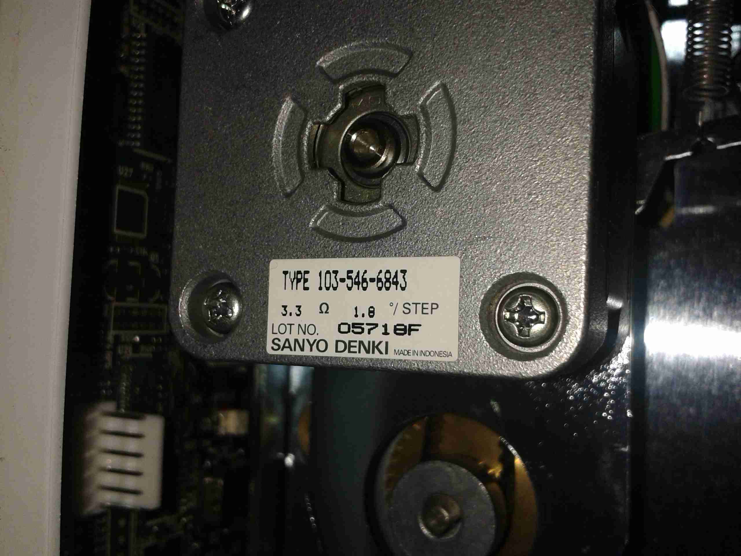
Main Stepper
The stepper itself is a quality ball-bearing Sanyo Denki bipolar motor.
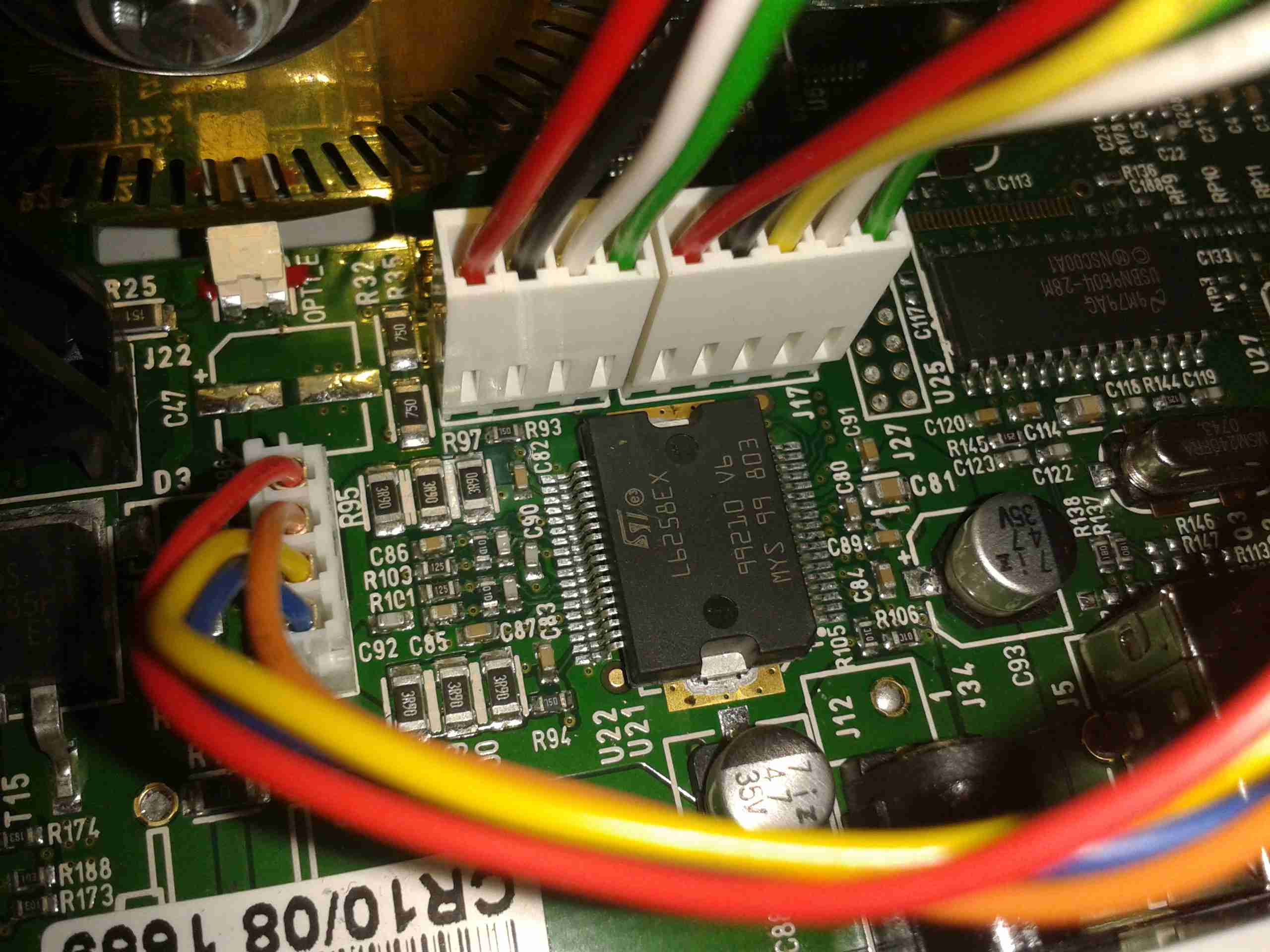
Main Stepper Driver
Electrical drive is provided to the stepper with a L6258EX DMOS universal motor driver. This chip can also drive DC motors as well as steppers.
Ribbon Supply Spool
Here is the encoder geared onto the ribbon supply spool. This is used to monitor the speed the ribbon is moving relative to the card.
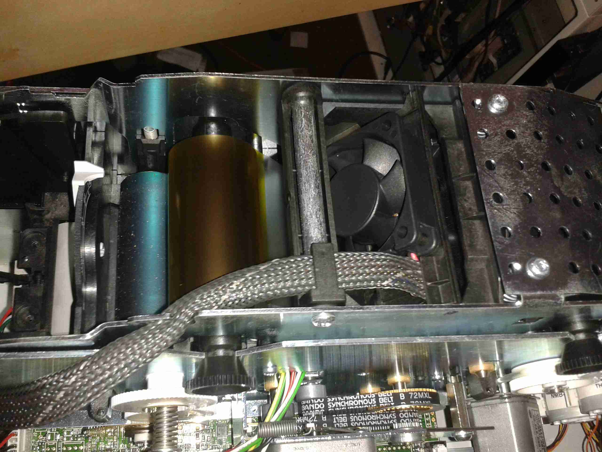
Printer Top
Here’s a top view through the printer, the blue roller on the left cleans the card as it’s pulled from the feeder, the gold coloured spool to it’s right is the ribbon supply reel. The cooling fan on the right serves to stop the print head overheating during heavy use.
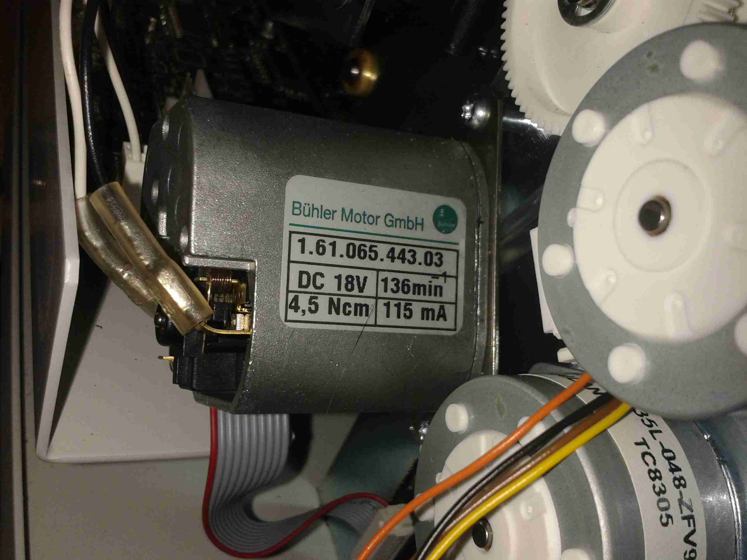
Spool Take Up Motor
The spool take-up reel is powered by another very high quality motor, a Buhler DC gearmotor. These printers are very heavily over engineered!
This motor drives the spool through an O-Ring belt, before the gear above. This allows the drive to slip in the event the ribbon jams, preventing it from breaking.
Duplex Unit Stepper Drivers
The pair of steppers that operate the duplexing unit are driven by a separate board, with a pair of L6219DS bipolar stepper driver ICs. There are also a couple of opto-sensors on this board for the output hopper.
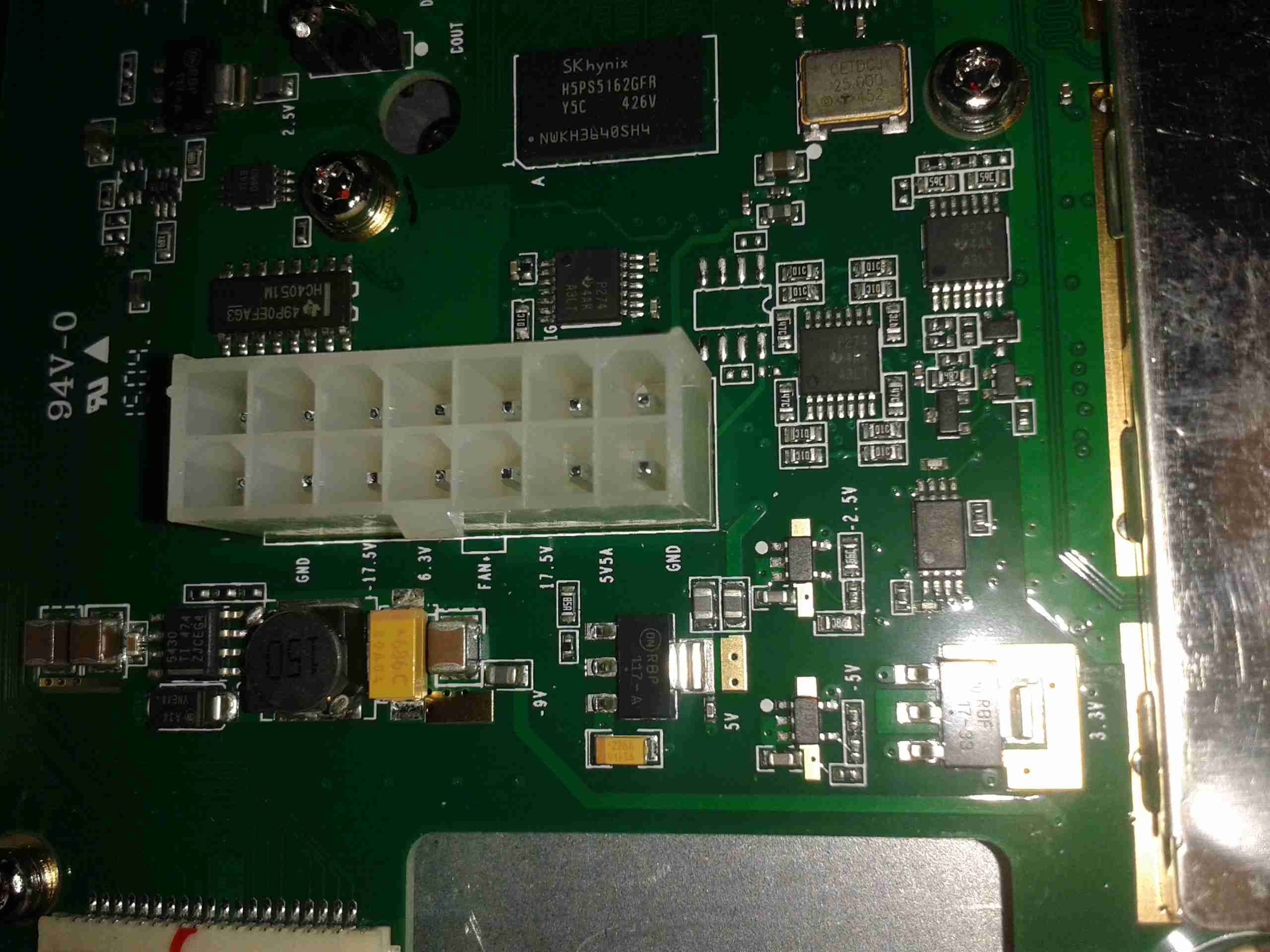
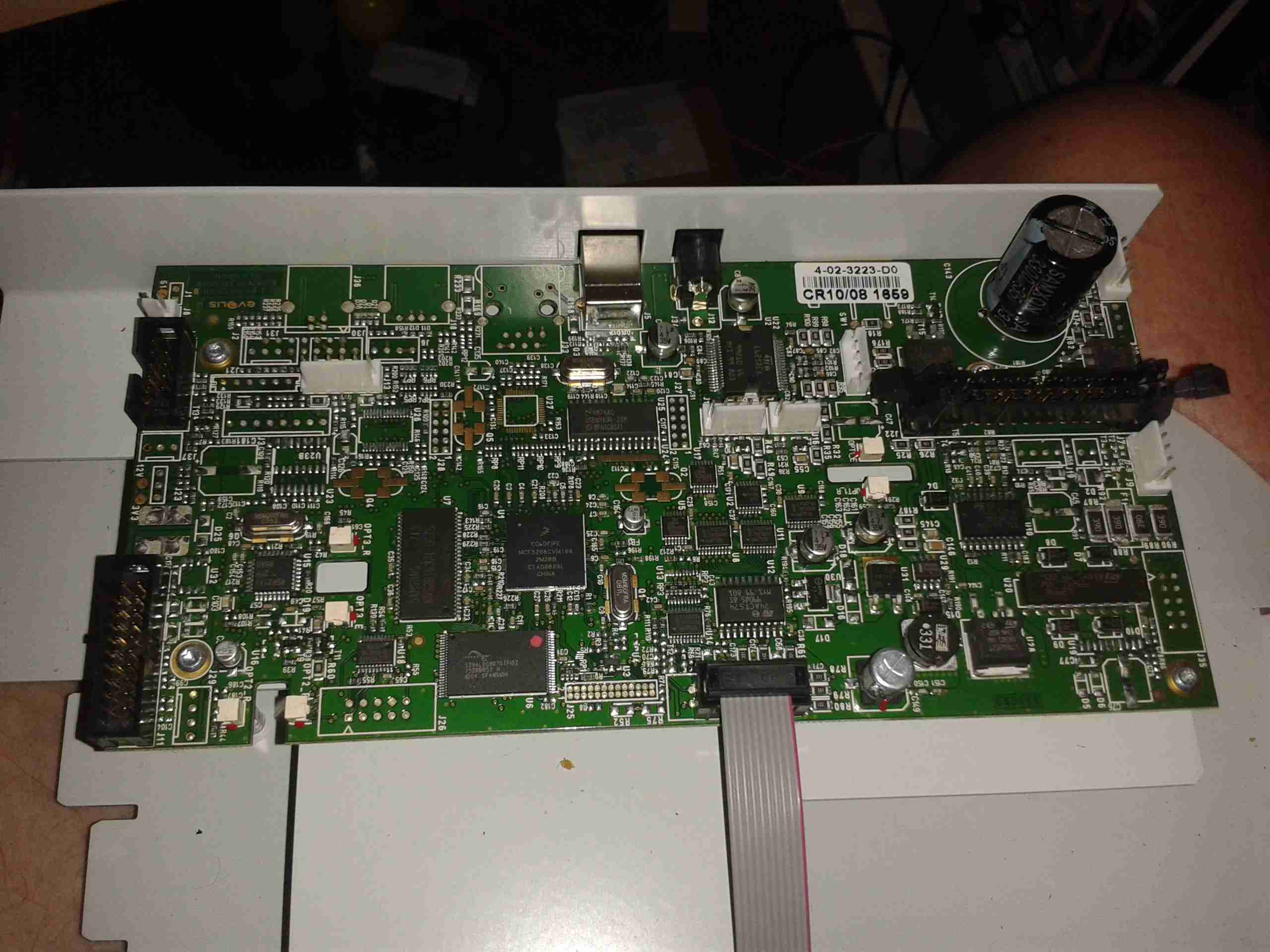
Main Control PCB
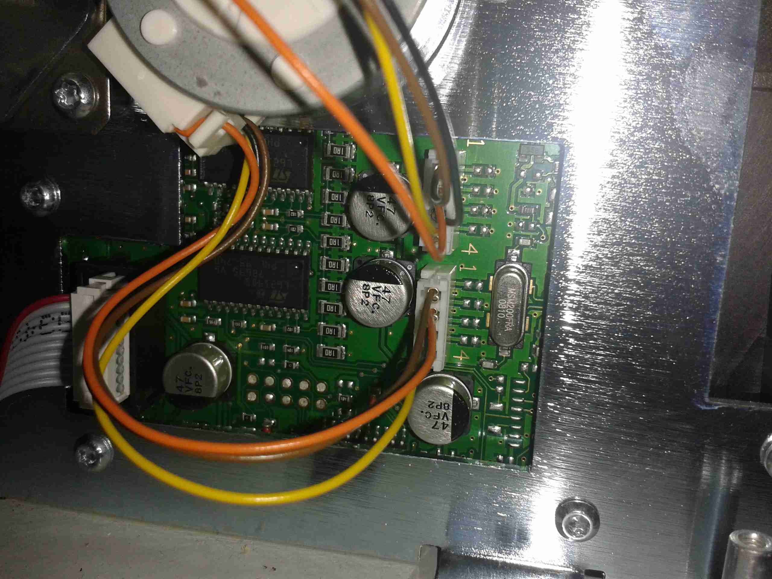
All the mechanisms of the printer are controlled from this main PCB, which handles all logic & power supply functions. Sections on the board are unpopulated, these would be for the Ethernet interface, smart card programming & magstripe programming.
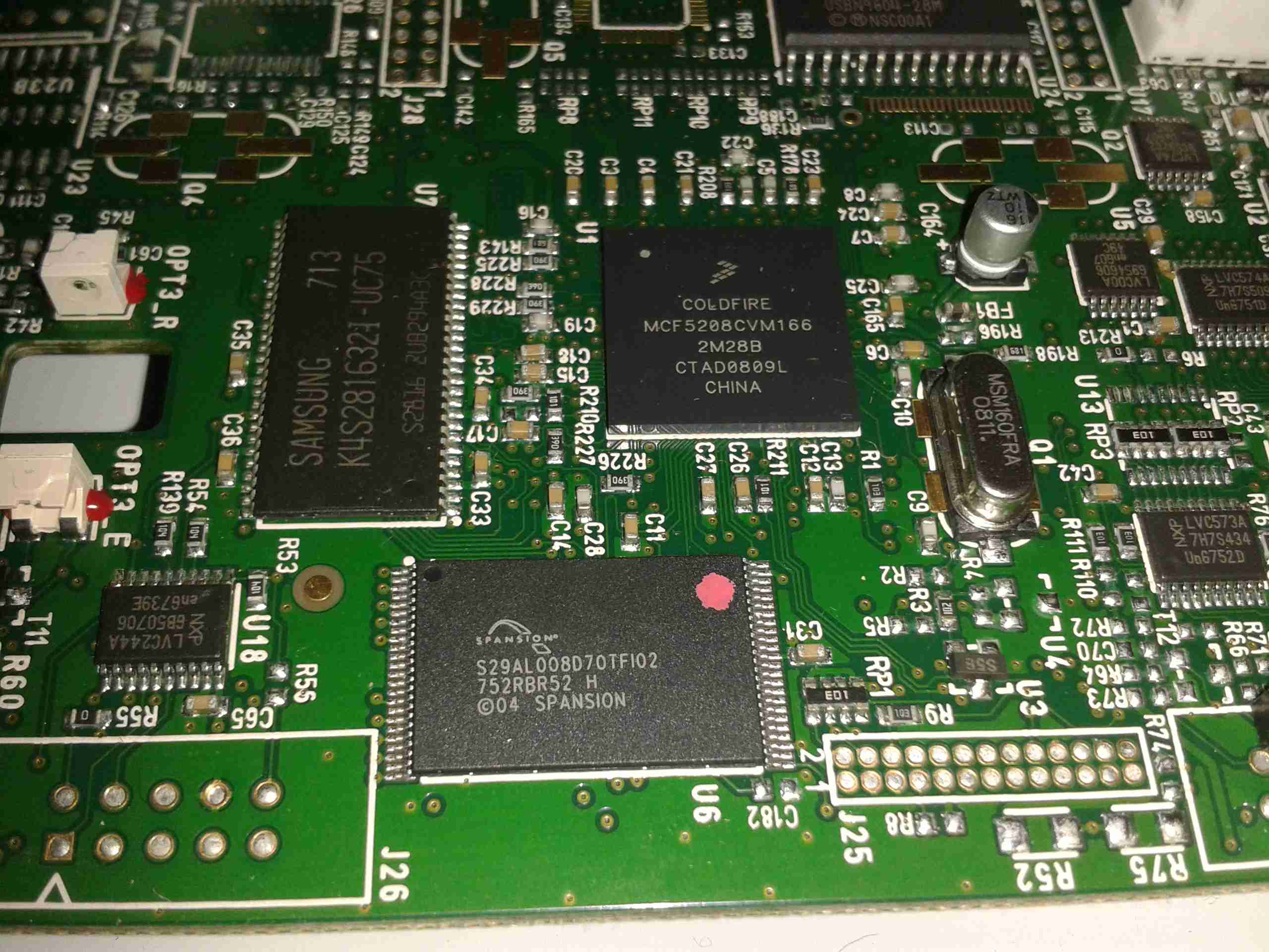
Main CPU
The brains of the operation is this ColdFire MCF5208CVM166 32-bit microprocessor. It features 16KB of RAM, 8KB of cache, DMA controller, 3 UARTs, SPI, 10/100M Ethernet and low power management. This is a fairly powerful processor, running at 166MHz.
It’s paired with an external 128Mbit SDRAM from Samsung, and a Spansion 8Mbit boot sector flash, for firmware storage.
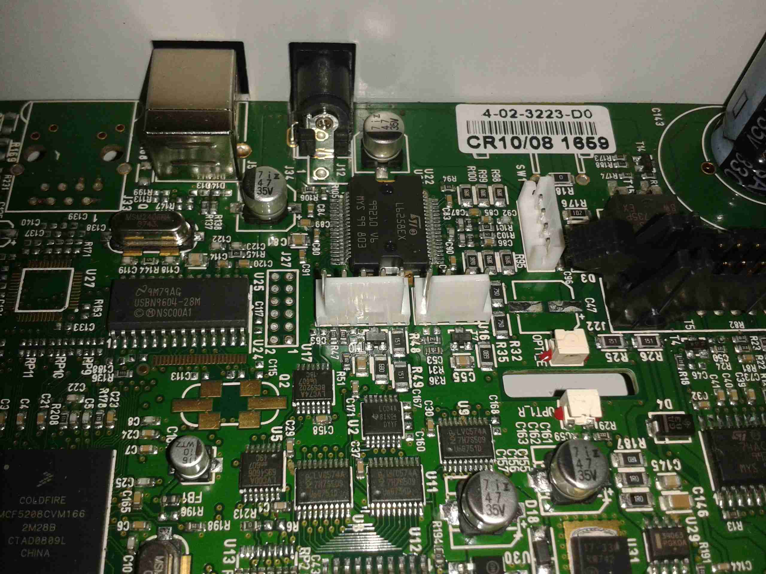
USB Interface & Power Input
Here the USB interface IC is located. It’s a USBN9604 from Texas Instruments, this interfaces with the main CPU via serial.
Following on from my recent power supply build, I’ve added on a couple of improvements:
Front Panel
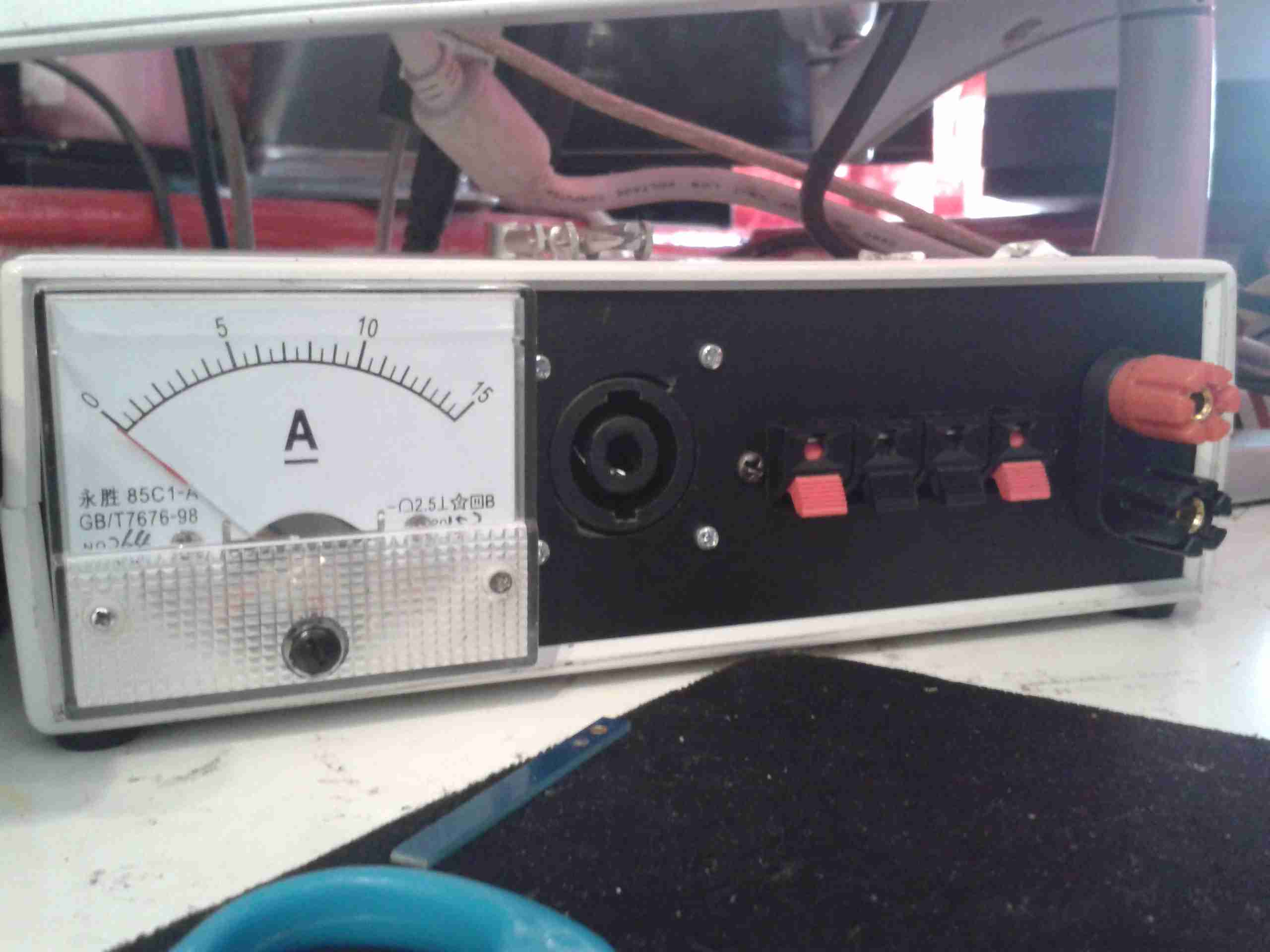
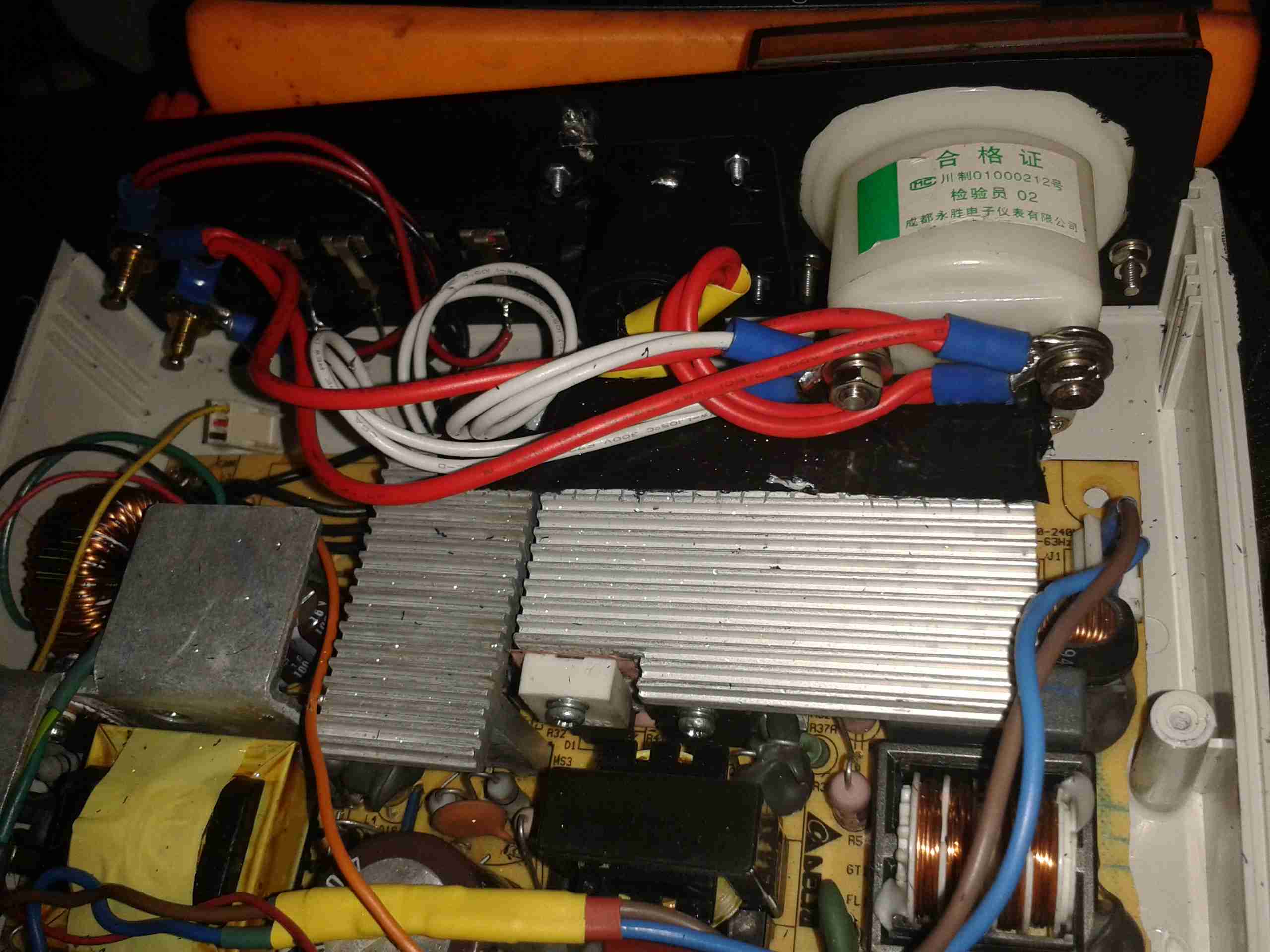
I’ve added on my standard SpeakOn type 30A connector, a bank of push terminals for quick connecting test leads, and a 15A FSD ammeter.
Panel Rear
Due to the limited space inside the supply, I’ve had to improvise some insulation on the mains-side heatsink to prevent a nasty accident. The heatsinks are tied to the supply’s HVDC bus negative, so they are energized at -145v DC relative to mains earth. This fact has given me a nasty surprise! The insulation is several layers of Kapton tape, with a couple of layers of Duct Tape. This along with trirated wire to the SpeakOn & the panel meter should ensure safety.
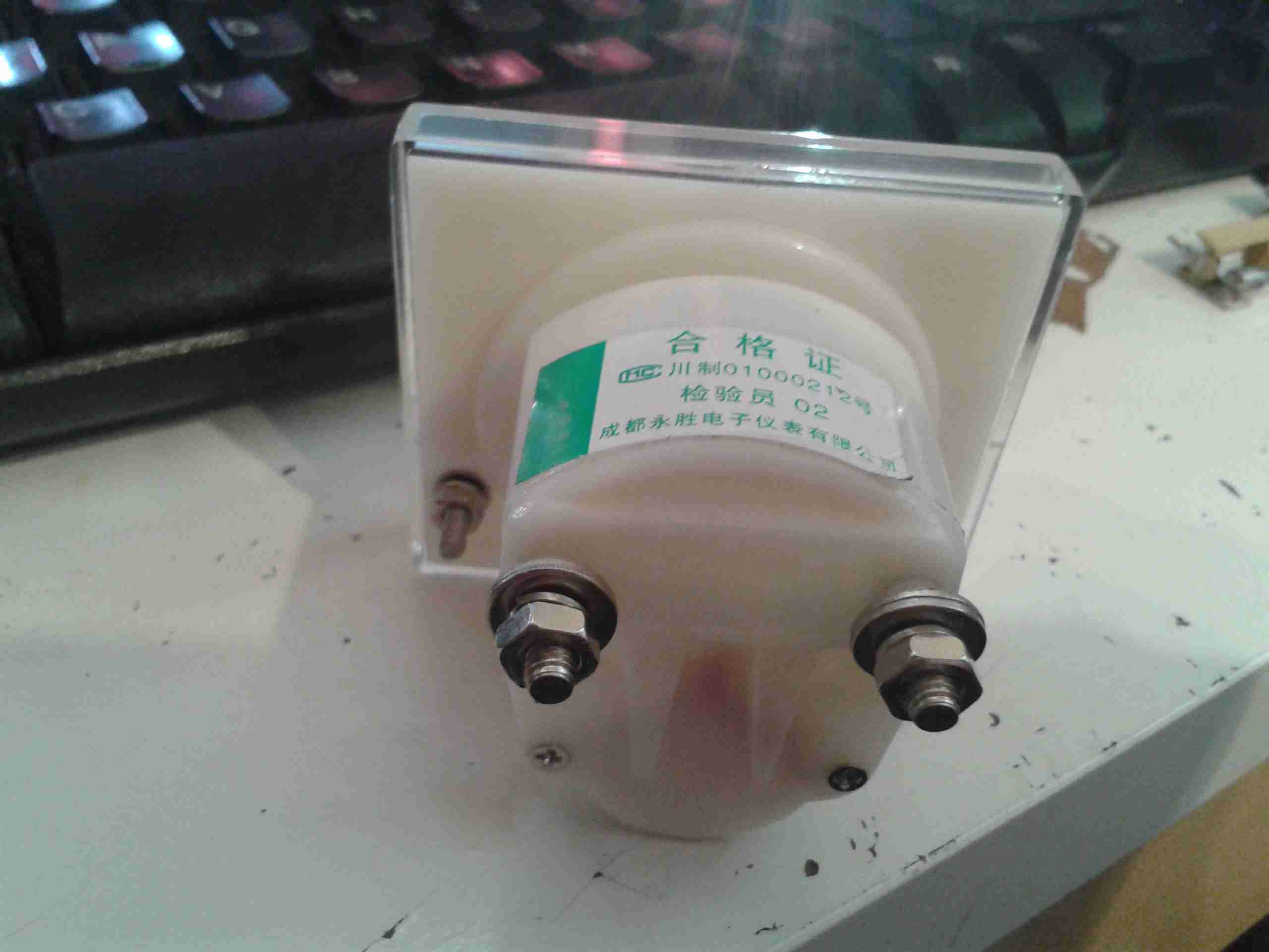
The Ammeter itself was sourced from eBay, for £2. It seems pretty accurate so far!
Ammeter
The shunt is built into the rear of these meters, in an ultrasonically welded part of the case, so I can’t examine it. Hopefully it is indeed rated to 15A!
The only things left to make this supply complete are a mains power switch, and a fan speed control, as the fan I have used is a little noisy at full speed. It will be good to get the speed based from the internal temperature, so the fan only runs at full speed when the supply is under load.
In my shack, 99% of my gear is all 12v powered, which is good for a few reasons:
Single Power Supply – This increases efficiency, as I’m only getting the losses of a single supply.
Safety – Mains voltages are dangerous, I’m not fond of working on such equipment.
Portability – I can power everything pretty much no matter were I am from a convenient car battery.
Convenience – Since everything is single supply, with all the same plugs, I don’t have to think about what goes where. This is more important due to my forgetfulness ;).
The one piece of equipment I regularly use that isn’t 12v is my soldering station. This is a Maplin A55KJ digital unit, which uses a 24v heating element.
While the soldering wand works OK when hooked direct to a 12v power supply (only at half power though), this removes the convenience of having temperature control.
The circuitry inside the unit is PIC microcontroller based, and doesn’t even bother rectifying the AC from the supply transformer before it’s sent to the heater. Because of this there are several reasons why I can’t just hook a DC-DC converter up to it to give it 24v.
It’s sensing the zero-crossing for the triac switch, to reduce heat dissipation, so it refuses to work at all with DC.
On looking at the Great Google, I found a project on Dangerous Prototypes, an Arduino based PID controller for soldering irons.
This requires that the soldering wand itself contains a thermocouple sensor – as the Maplin one I have is a cheap copy of the Atten 938D, it doesn’t actually use a thermocouple for temperature sensing. It appears to read the resistance of the element itself – Nichrome heating elements change resistance significantly depending on temperature.
I’ve managed to find a source of cheap irons on eBay, with built in thermocouples, so I’ve got a couple on order to do some testing with. While I wait for those to arrive, I’ve prototyped up the circuit on breadboard for testing:
Prototype
I’ve remapped some of the Arduino pins, to make PCB layout less of a headache, but the system is working OK so far, with manual input for the sensed temperature.
I’m using an IRL520N logic-level HEXFET for the power switching, rated at 10A. As the irons only draw a max of 4.5A, this is plenty beefy enough.
To come up with the +24v supply for the heater, a small DC-DC converter will be used.
More to come when the components for the thermocouple amplifier arrive, and the soldering irons themselves!
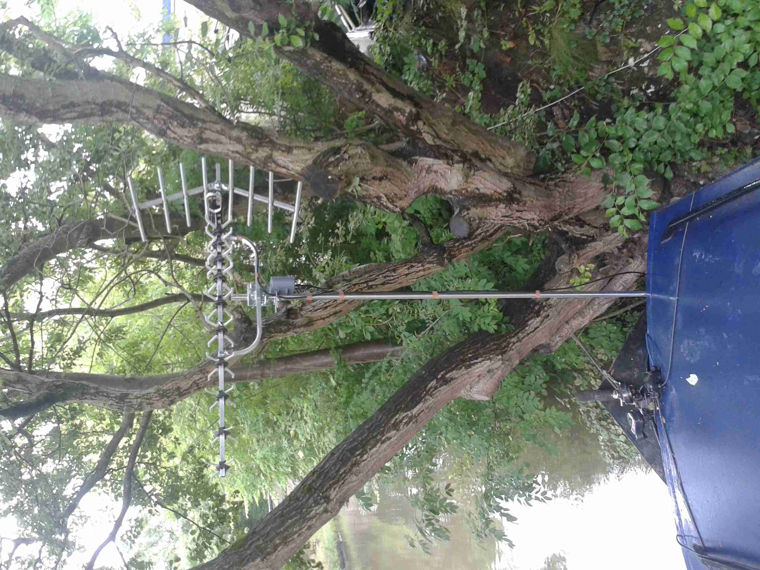
Here’s the final instalment of the new high gain TV antenna & it’s masthead amplifier.
High Gain Antenna
Here’s the new antenna on it’s removable mast. This apparently will give 13db of gain over the old antenna. The masthead amplifier box is mounted just below.
Amplifier
Here’s the amplifier just below the antenna. I do hope the seals on this hold against the weather! The amplifier inside isn’t protected at all.
Amplifier Module
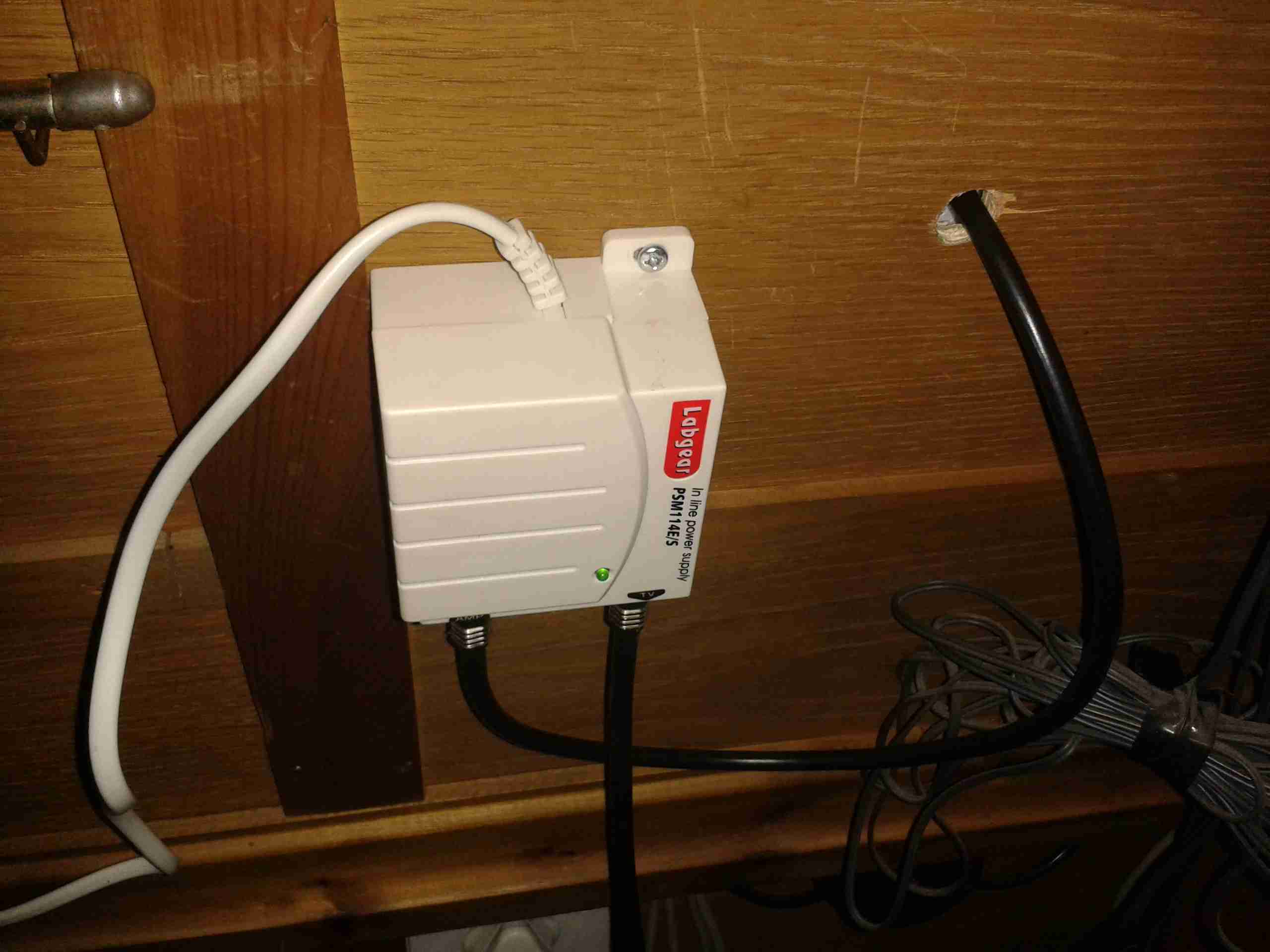
Here’s the module itself. This is powered by +12v injected into the coax with the power supply I previously modified. F-type connectors are used. (I don’t like these connector types, their lack of a true centre pin is poor design in my opinion).
Here’s the power supply, mounted behind the TV where the cable comes through the hull.
PSUAmplifier PCB
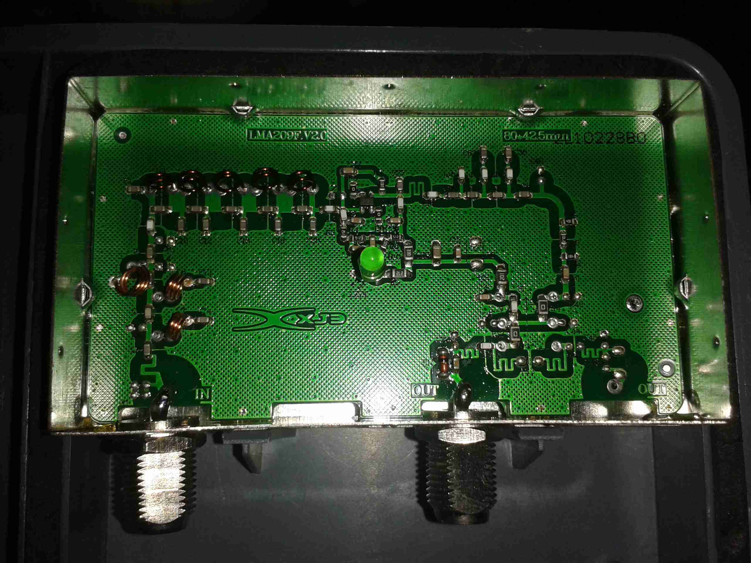
Here’s the inside of the amplifier module. It’s very simple, with some input filtering to block out 4G mobile signals, and a single amplifier transistor.
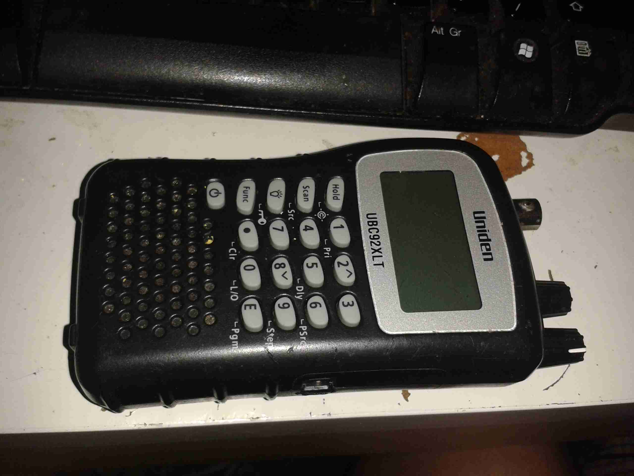
One bit of my equipment that I’ve never looked into is my scanner, a handheld Uniden unit. I got this when Maplin Electronics had them on special offer a few years ago.
Uniden Scanner
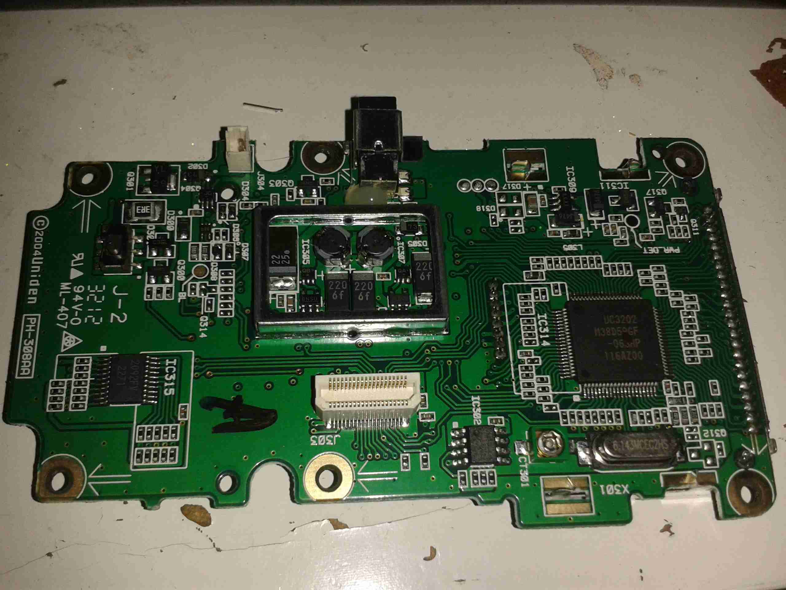
Here’s the scanner itself, roughly the same size as a usual HT.
Back Cover Removed
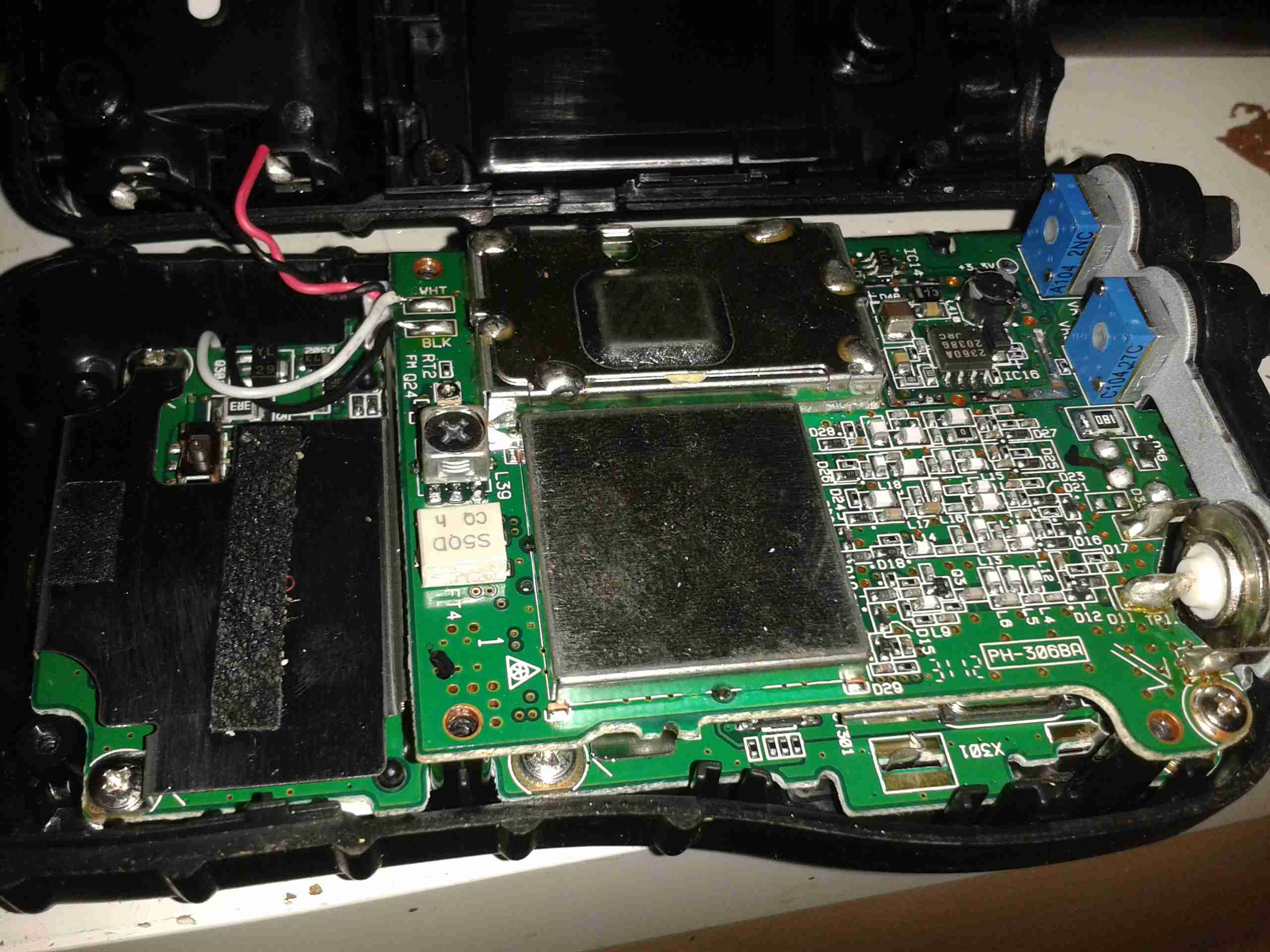
Here the back cover has been removed, and the main RF board is visible at the top of the stack. Unfortunately the shielding cans are soldered on this unit, so no looking under there 🙁
On the right hand side of the board next to the antenna input is the main RF filter network, and it’s associated switching. The RF front end is under the shield closest to the front edge.
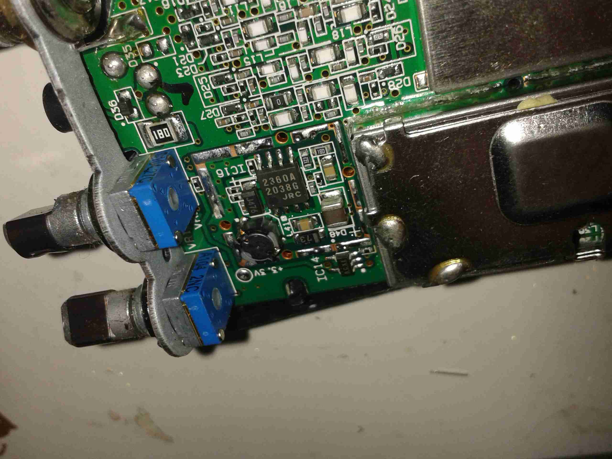
Controls & 3.3v Regulator
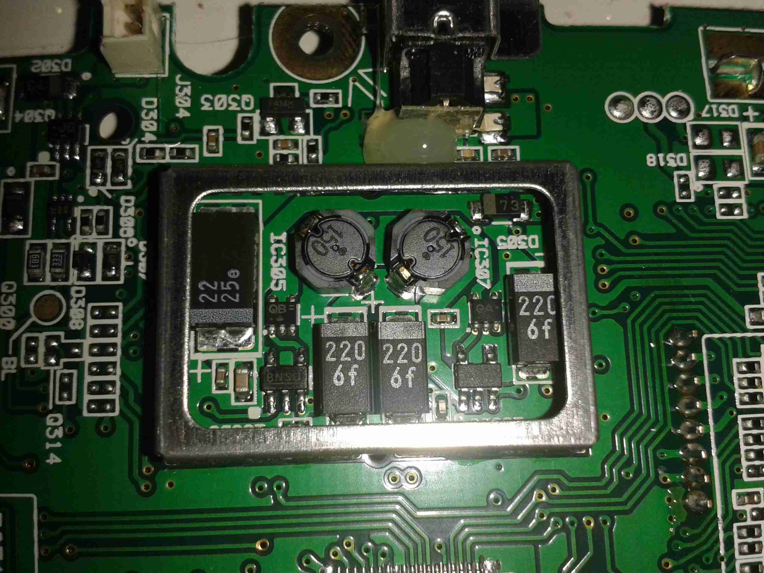
On the other side of the PCB is the Volume & Squelch potentiometers, along with a dedicated 3.3v switching supply. An NJM2360A High Precision DC/DC converter IC controls this one. A 3.3v test point is visible next to the regulator.
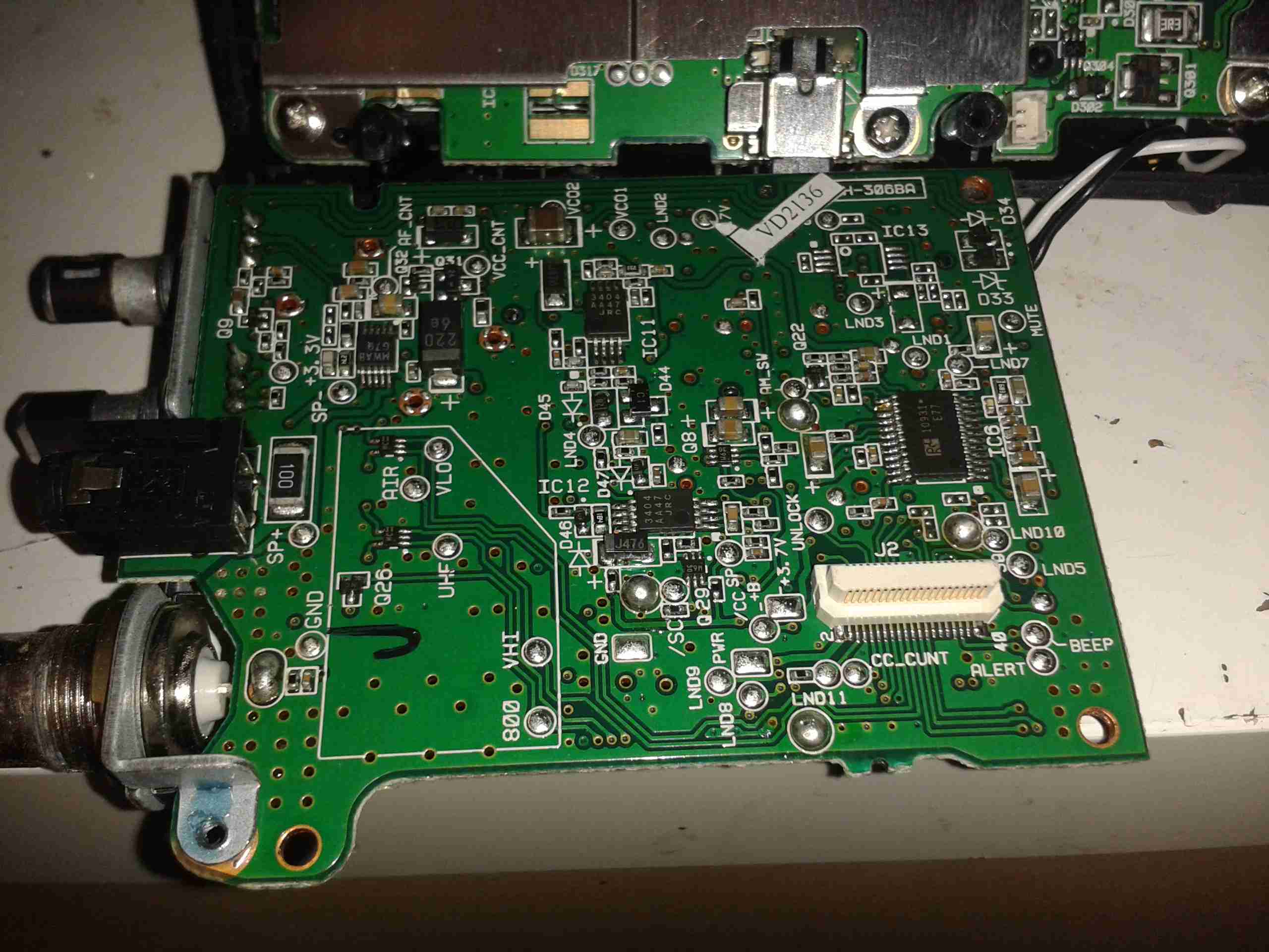
RF Board Reverse
Here’s the backside of the RF board, some more interesting parts here. There’s a pair of NJM3404A Single Supply Dual Op-Amp ICs, and a TK10931V Dual AM/FM IF Discriminator IC. This is the one that does all the back-end radio functionality. The audio amplifier for the internal speaker & external headphone jack is also on this PCB, top left. A board-to-board interconnect links this radio board with the main control board underneath.
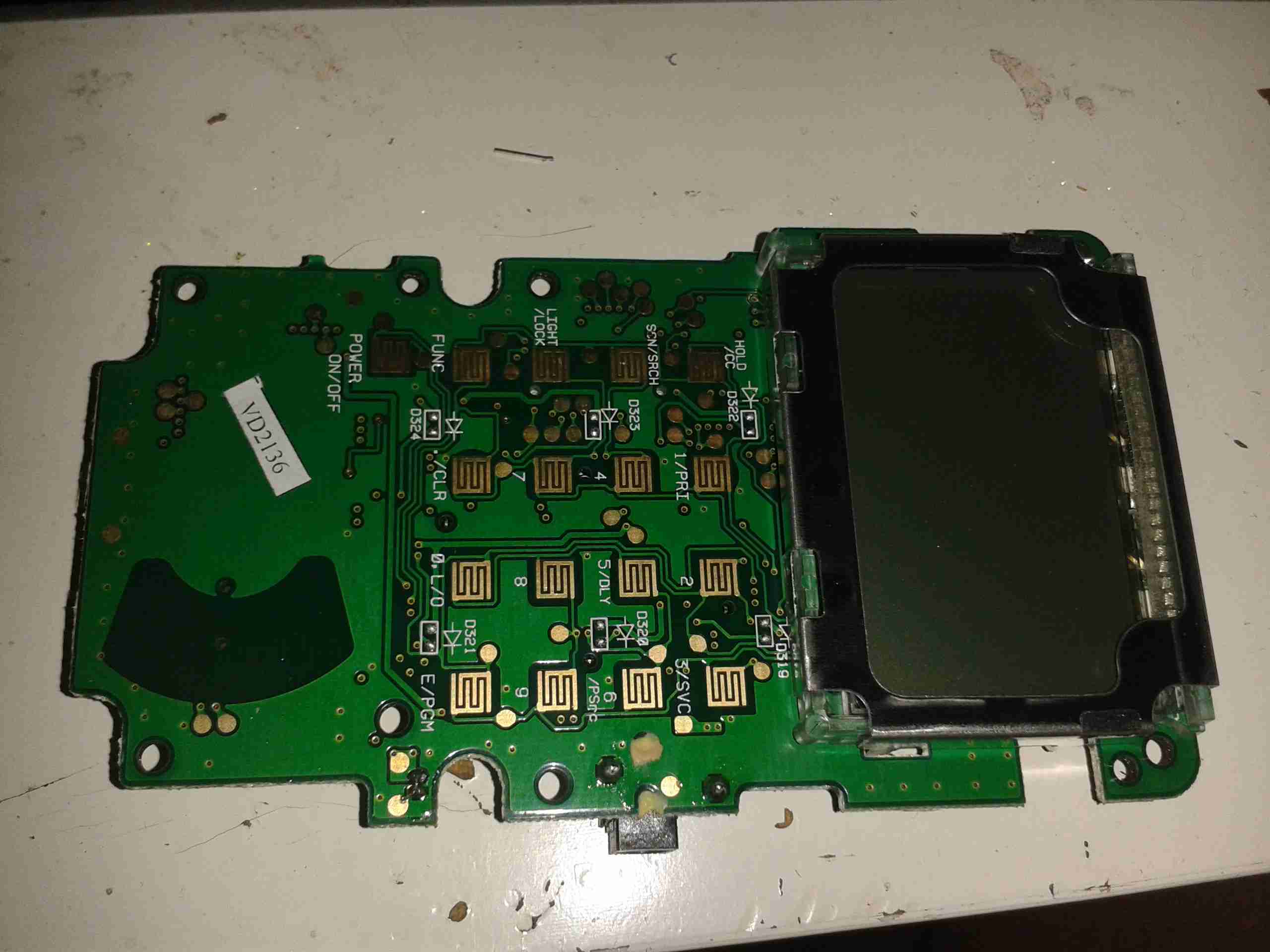
Control PCB Front
Here’s the front of the control PCB, nothing much to see here, just the LCD & membrane keypad contacts.
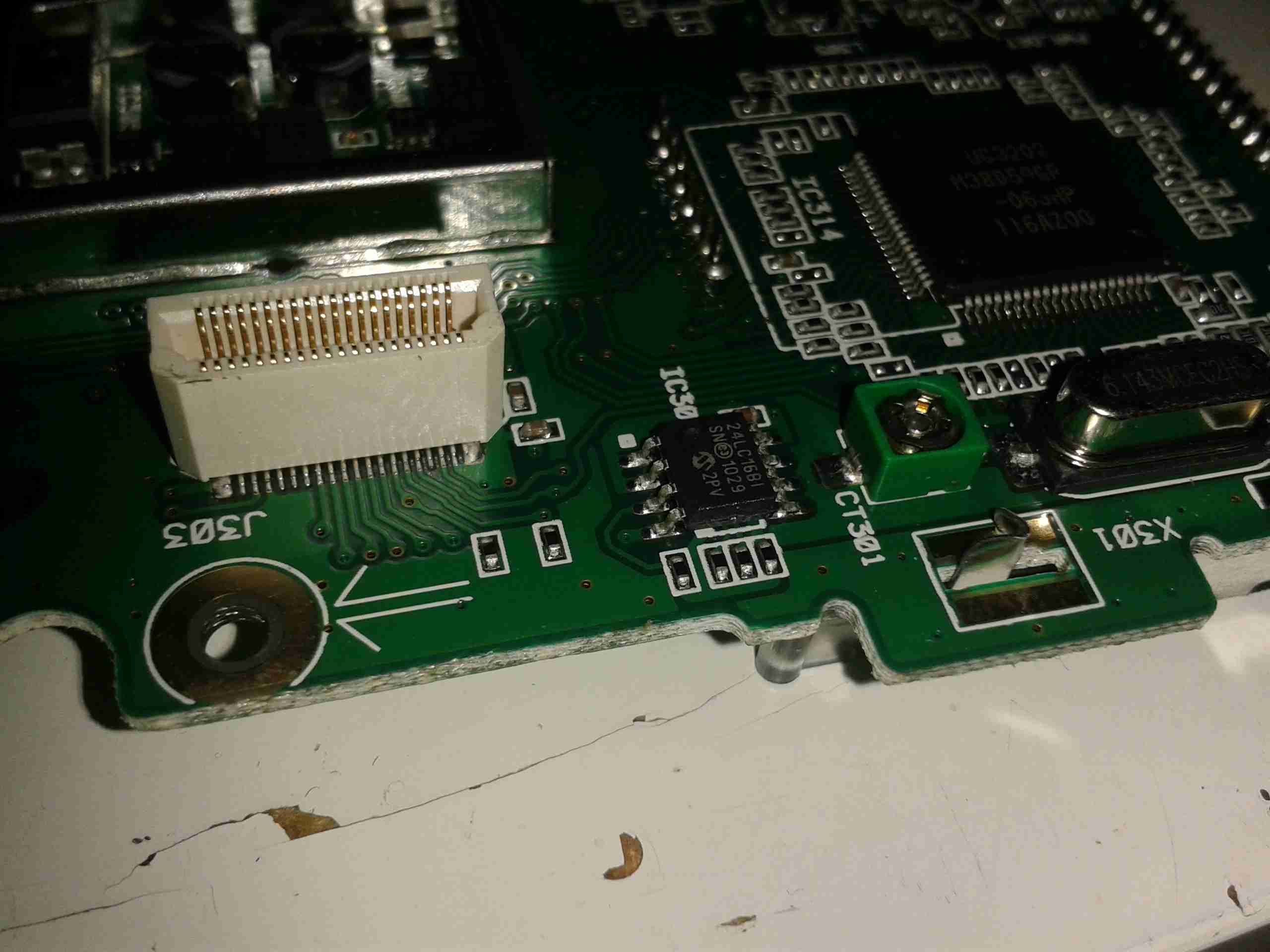
Control PCB Reverse
And here’s the reverse side of the control board. All the interesting bits are here. The main microcontroller is on the right, a Renesas M38D59GF, a fairly powerful MCU, with onboard LCD drive, A/D converter, serial interface, 60K of ROM & 2K of RAM. It’s 6.143MHz clock crystal is just below it.
The mating connector for the RF board is in the centre here.
There is also a Microchip 24LC168 16KB I²C EEPROM next to the main microcontroller. This is probably for storing user settings, frequencies, etc.
EEPROM
The rest of this board is dedicated to battery charging and power supply, in the centre is a dual switching controller, I can’t figure out the numbers on the tiny SOT23 components in here, but this is dealing with the DC 6v input & to the left of that is the circuitry for charging the NiMH cells included with the scanner.
PSU
The last bit of this PCB is a BU2092FV Serial In / Parallel Out 4 channel driver. Not sure what this one is doing, it might be doing some signal multiplexing for the RF board interface. Unfortunately the tracks from this IC are routed on the inner layers of the board so they can’t be traced out.
Onboard the boat we have a small issue with a weak TV signal, and this coupled with a 60′ long run of coax is an issue. Due to the loss in the coax, we’ve lost most of the already weak signal.
To try & solve this issue, I’m fitting a masthead amplifier unit.
These amplifiers are fed power down the same coax that’s carrying the RF signal, and a special power supply is supplied with the amplifier for this. However it’s only 240v AC, no 12v version available.
Here’s the power supply unit, which fits into the coax between the TV & the antenna.
Amplifier Supply
Luckily the 240v supply is easily removable & here has been replaced with a 12v regulator.
New Supply
There’s not very much inside the shielding can, just a few filter capacitors & an RF choke on the DC feed, to keep the RF out of the power supply system.
The original cable is used, so the supply doesn’t even look like it’s been modified from the outside.
More to come on this when I get the amplifier installed along with the new coax run 🙂
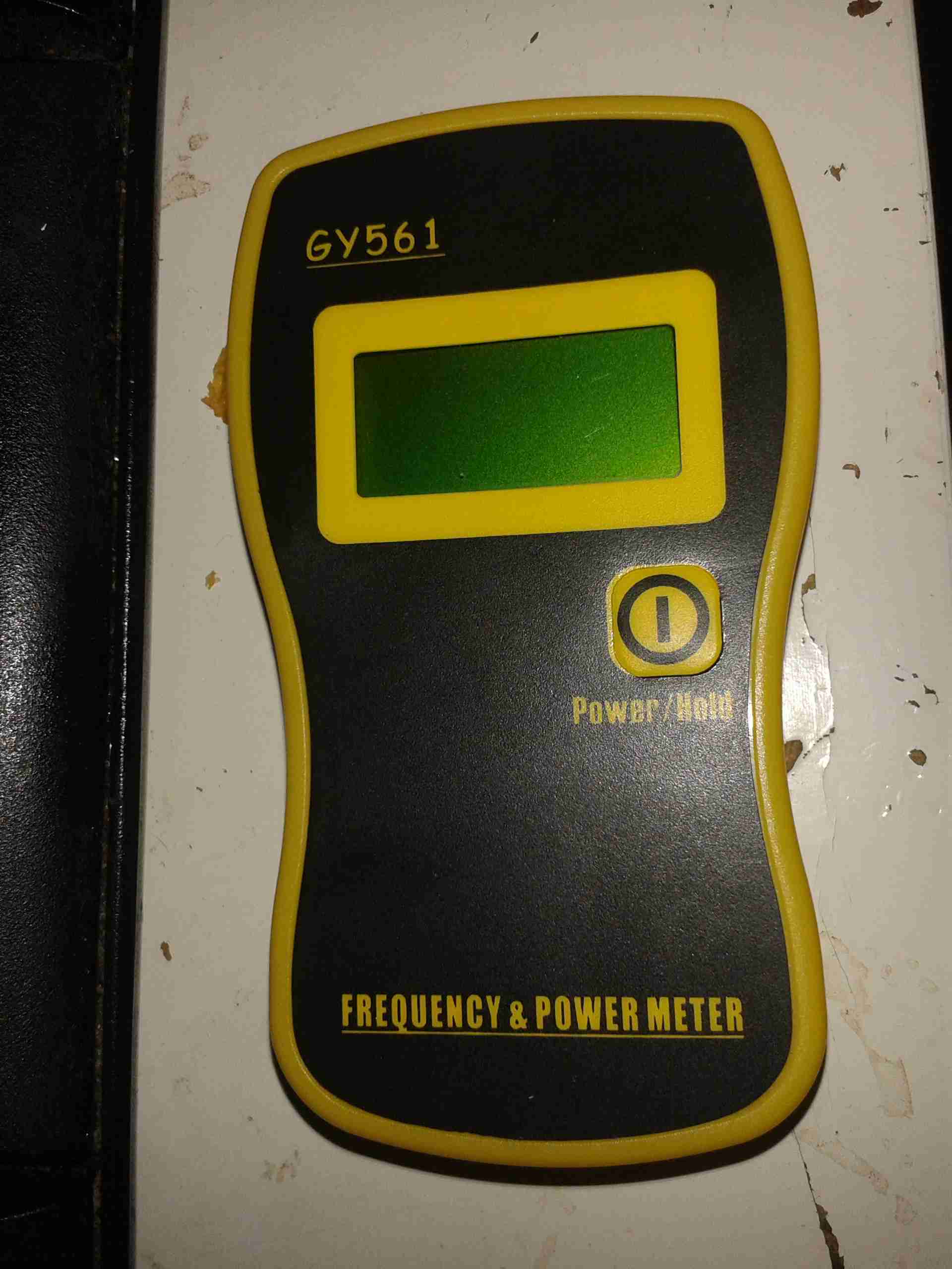
The latest addition to my radio shack is the GY561 frequency & power meter, which has already come in useful for measuring the output power of all my radios.
GY561
It’s a small device, roughly the same size & weight as a stock UV-5R. Power is provided by 3 AAA cells.
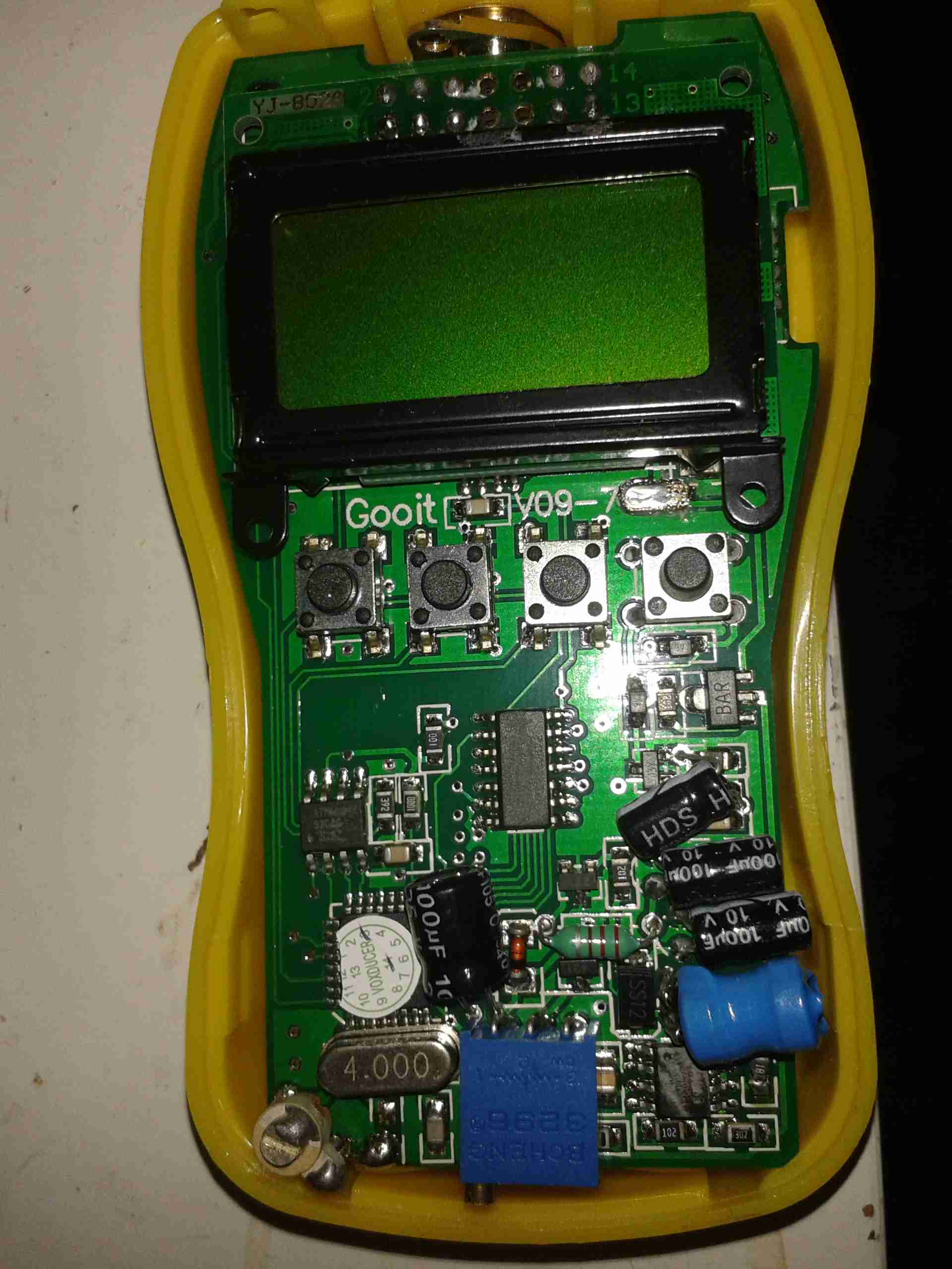
Display
The display is a standard HD44780 8×2 module. The display on this unit isn’t backlit, so no operating in the dark.
Cover Removed
The cover pops off easily to allow access to the internals, without having to remove any screws!
The 4 screws on the back of the unit hold the heatsink plate for the 50W 50Ω dummy load resistor.
Removing the cover reveals a couple of adjustments, for frequency & RF power calibration.
There are also 3 tactile switches that aren’t on the front panel. According to the manual (which in itself is a masterpiece of Chinglish), they are used to software calibrate the unit if an accurate RF power source is available. I will attempt to do a reasonable translation when time allows.
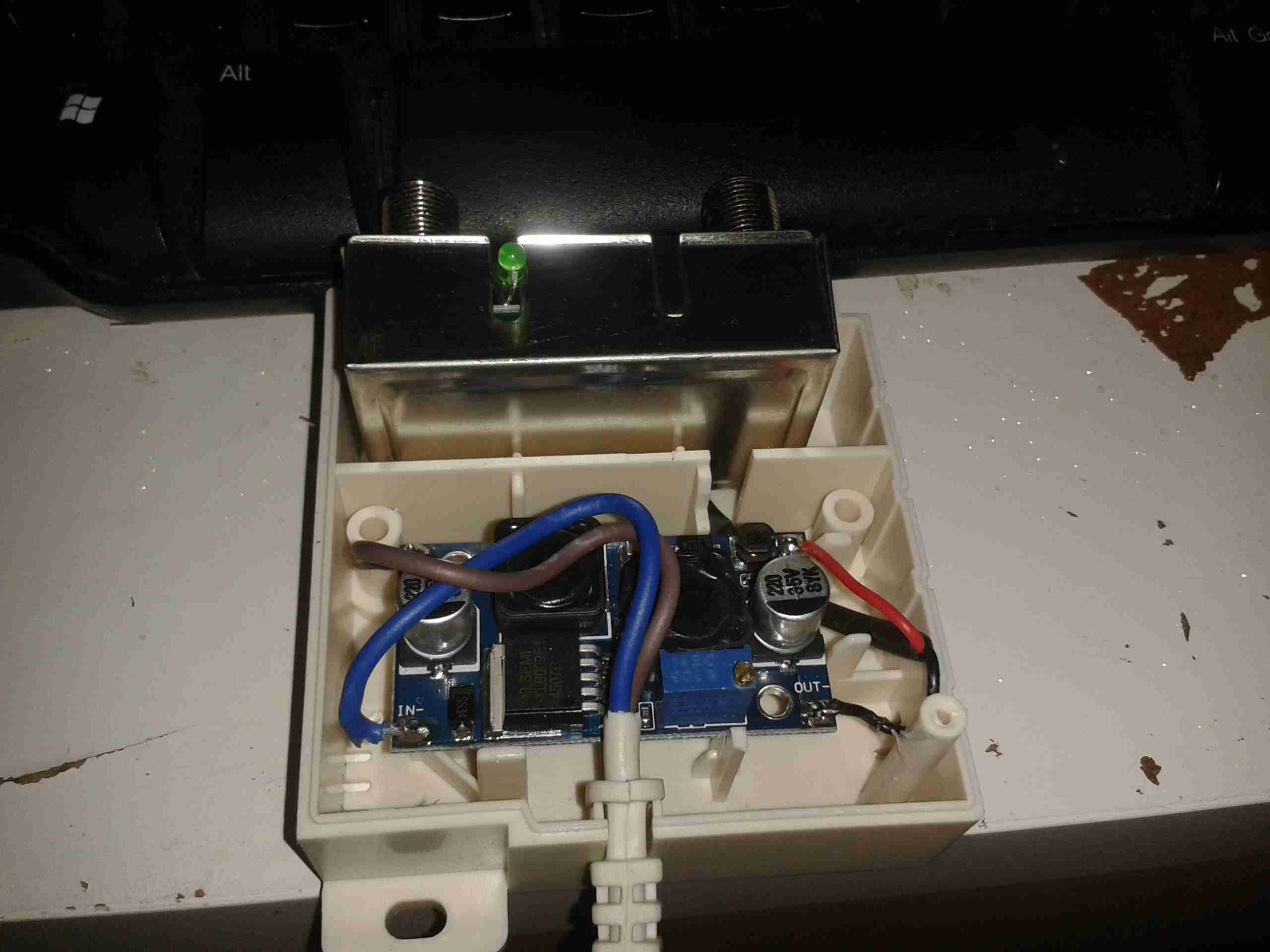
Disassembly further than this involves some desoldering in awkward places, so a search of the internet revealed an image of the rest of the internal components. In the case of my meter, all the part numbers have been scrubbed off the ICs in an attempt to hide their purpose. While it’s possible to cross-reference IC databooks & find the part numbers manually, this process is a time consuming one. Luckily the image I managed to locate doesn’t have the numbers scrubbed.
Total Disassembly
Under the LCD is some 74HC series logic, and a prescaler IC as seen in the previous frequency counter post. However in this unit the prescaler is a MB506 microwave band version to handle the higher frequencies specified.
In this case however the main microcontroller is an ATMEGA8L.
This is complemented by a SN54HC393 4-bit binary counter for the frequency side of things. This seems to make it much more usable down to lower frequencies, although the manual is very generous in this regard, stating that it’s capable of reading down to 1kHz. In practice I’ve found the lowest it reliably reads the frequency input is 10MHz, using my AD9850 DDS VFO Module as a signal source.
It did however read slightly high on all readings with the DDS, but this could have been due to the low power output of the frequency source.
Just like the other frequency counter module, this also uses a trimmer capacitor to adjust the microcontroller’s clock frequency to adjust the calibration.
The power supply circuitry is in the bottom left corner of the board, in this case a small switching supply. The switching regulator is needed to boost the +4.5v of the batteries to +5v for the logic.
Also, as the batteries discharge & their terminal voltage drops, the switching regulator will allow the circuit to carry on functioning. At present I am unsure of the lower battery voltage limit on the meter, but AAA cells are usually considered dead at 0.8v terminal voltage. (2.4v total for the 3 cells).
When turned on this meter draws 52mA from the battery, and assuming 1200mAh capacity for a decent brand-name AAA cell, this should give a battery life of 23 hours continuous use.
On the back of the main PCB is a 5v relay, which seems to be switching an input attenuator for higher power levels, although I only managed to trigger it on the 2m band.
Finally, right at the back attached to an aluminium plate, is the 50Ω dummy load resistor. This component will make up most of the cost of building these, at roughly £15.
On my DVM, this termination reads at about 46Ω, because of the other components on the board are skewing the reading. There are a pair of SMT resistors, at 200Ω & 390Ω in series, and these are connected across the 50Ω RF resistor, giving a total resistance of 46.094Ω.
This isn’t ideal, and the impedance mismatch will probably affect the calibration of the unit somewhat.
The heatsinking provided by the aluminium plate is minimal, and the unit gets noticeably warm within a couple of minutes measuring higher power levels.
High power readings should definitely be limited to very short periods, to prevent overheating.
The RF is sampled from the dummy load with a short piece of Teflon coax.
There’s a rubber duck antenna included, but this is pretty useless unless it’s almost in contact with the transmitting antenna, as there’s no input amplification. It might be handy for detecting RF emissions from power supplies, etc.
For the total cost involved I’m not expecting miracles as far as accuracy is concerned, (the manual states +/-10% on power readings).
The frequency readout does seem to be pretty much spot on though, and the ability to calibrate against a known source is handy if I need some more accuracy in the future.
I’ve also done an SWR test on the dummy load, and the results aren’t good.
At 145.500 MHz, the SWR is 3:1, while at 433.500 it’s closer to 4:1. This is probably due to the lower than 50Ω I measured at the meter’s connector.
These SWR readings also wander around somewhat as the load resistor warms up under power.
I’ll probably also replace the AAA cells with a LiPo cell & associated charge/protection circuitry, to make the unit chargeable via USB. Avoiding disposable batteries is the goal.
There are times when I am frequently away from home base, usually either on the canal system or at a festival. During these times it’s very handy to be able to just grab a bag, without having to be concerned about sorting everything out.
This post will only detail the portable shack bag. The power supply kit that goes along with it with be detailed in another post.
The bag I use is an VHS Camcorder bag from the early 80’s. It’s very well built, & copes easily with the weight of all the radio gear.
Total weight for this system is 13.4lbs (6kg).
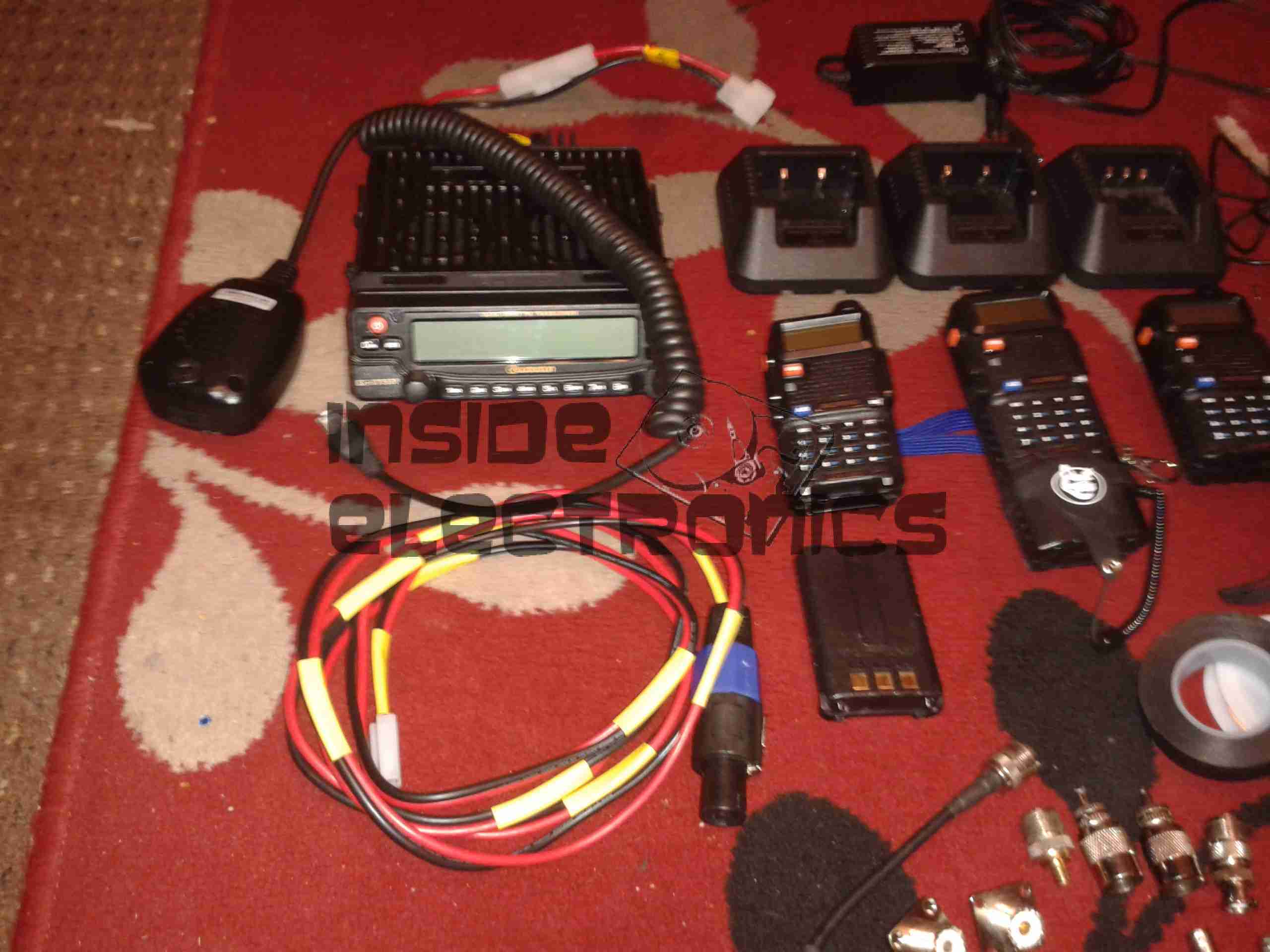
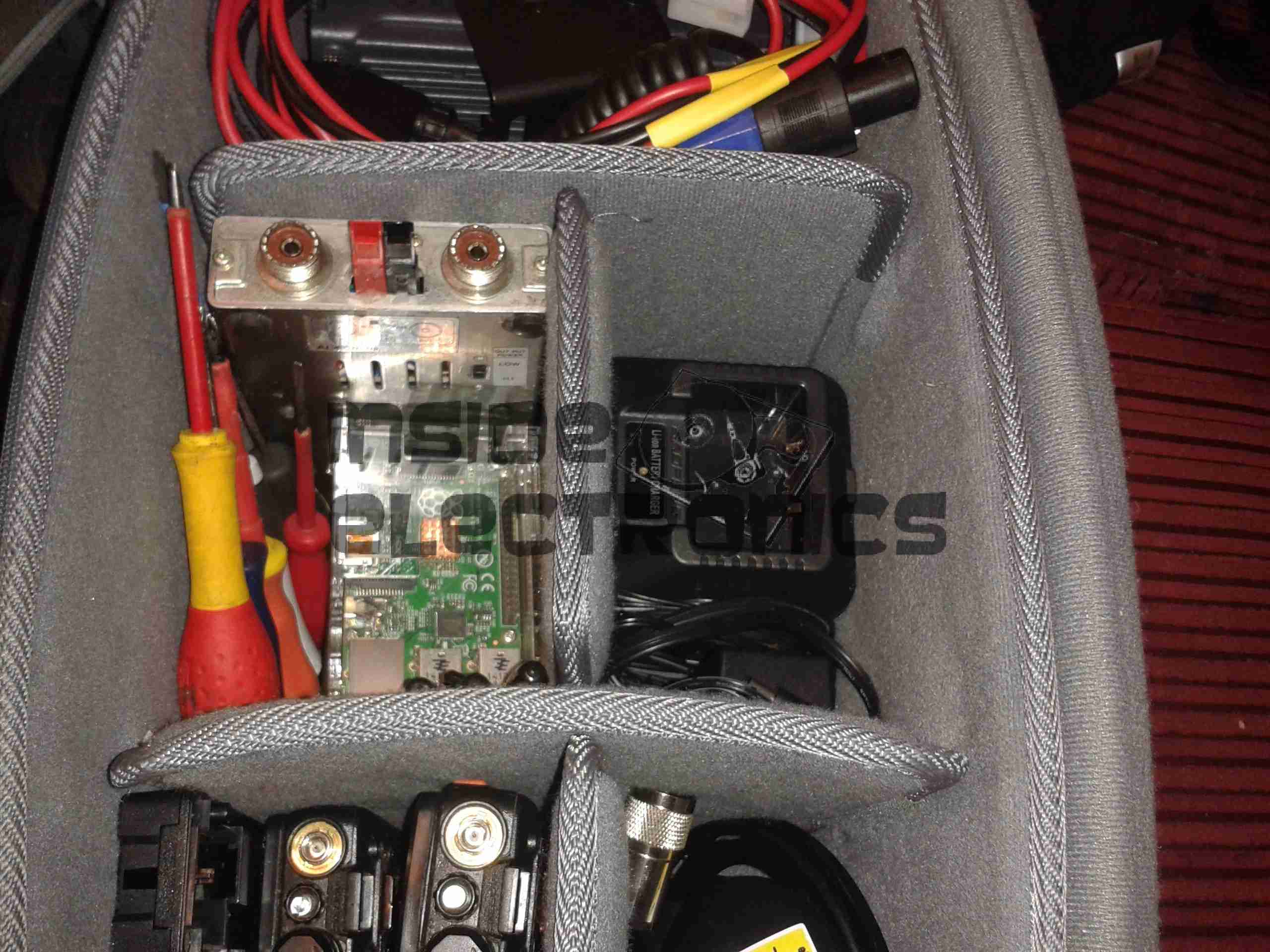
Mobile Radio Bag
Above is the bag packed. Obligatory International Ameteur Radio Symbol patch front & centre. Being an old camera bag, this easily slings over the shoulder, with it’s padded strap.
Current Equipment
Here is all the current equipment laid out. All the equipment to enable me to set up a station anywhere.
In the following photos I will go into the details.
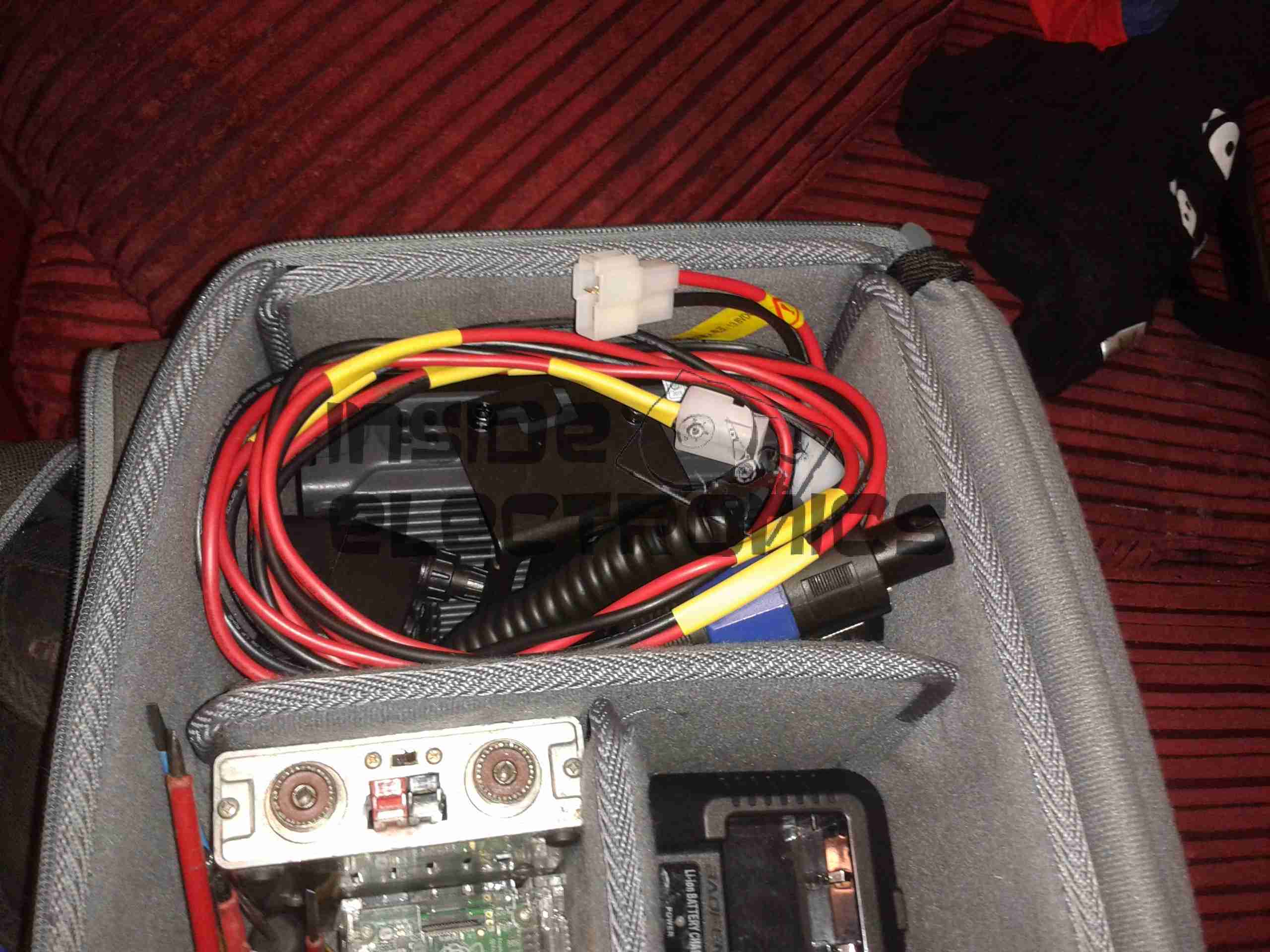
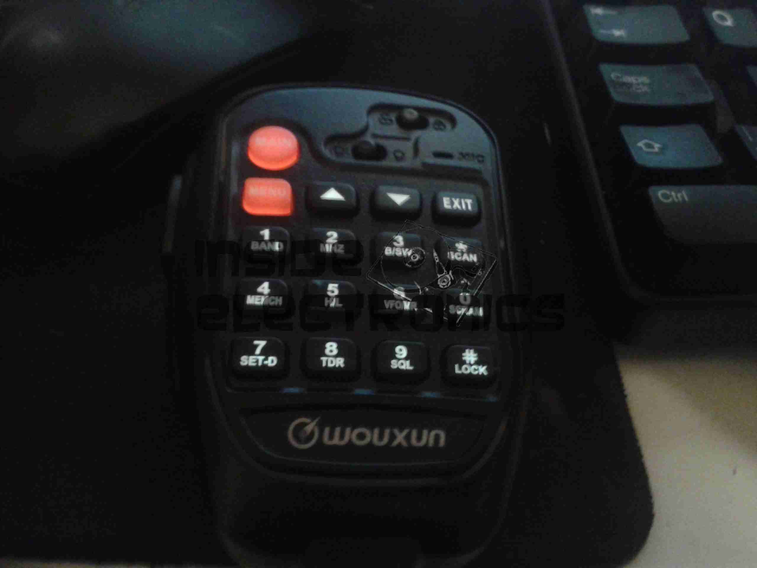
Main Radio
First off, my main radio. This is the same Wouxun KG-UV950P mobile rig I have posted about previously. I have heatshrunk the power cable to keep it together & attached my standard power connector to the end. More on these later on.
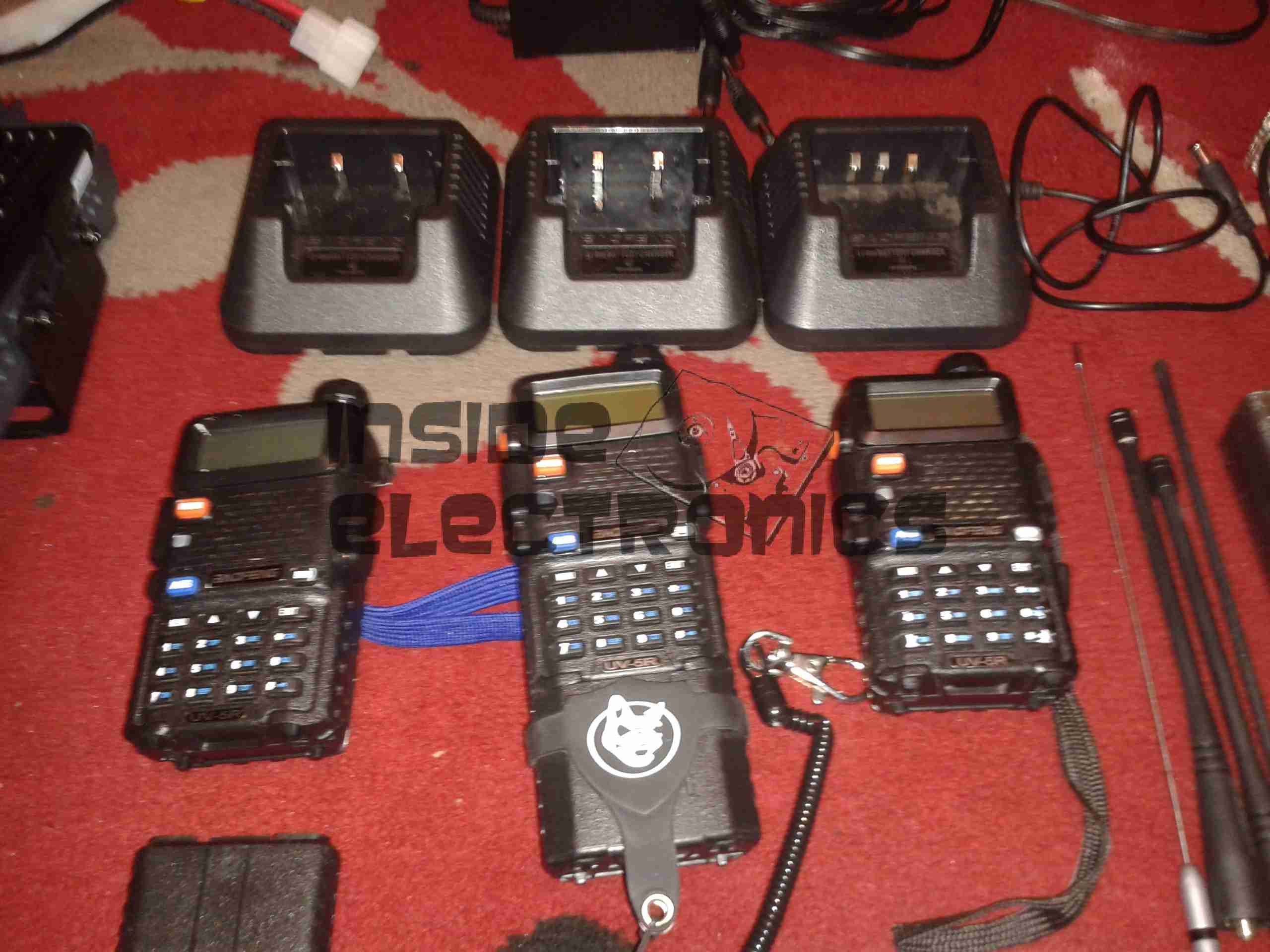
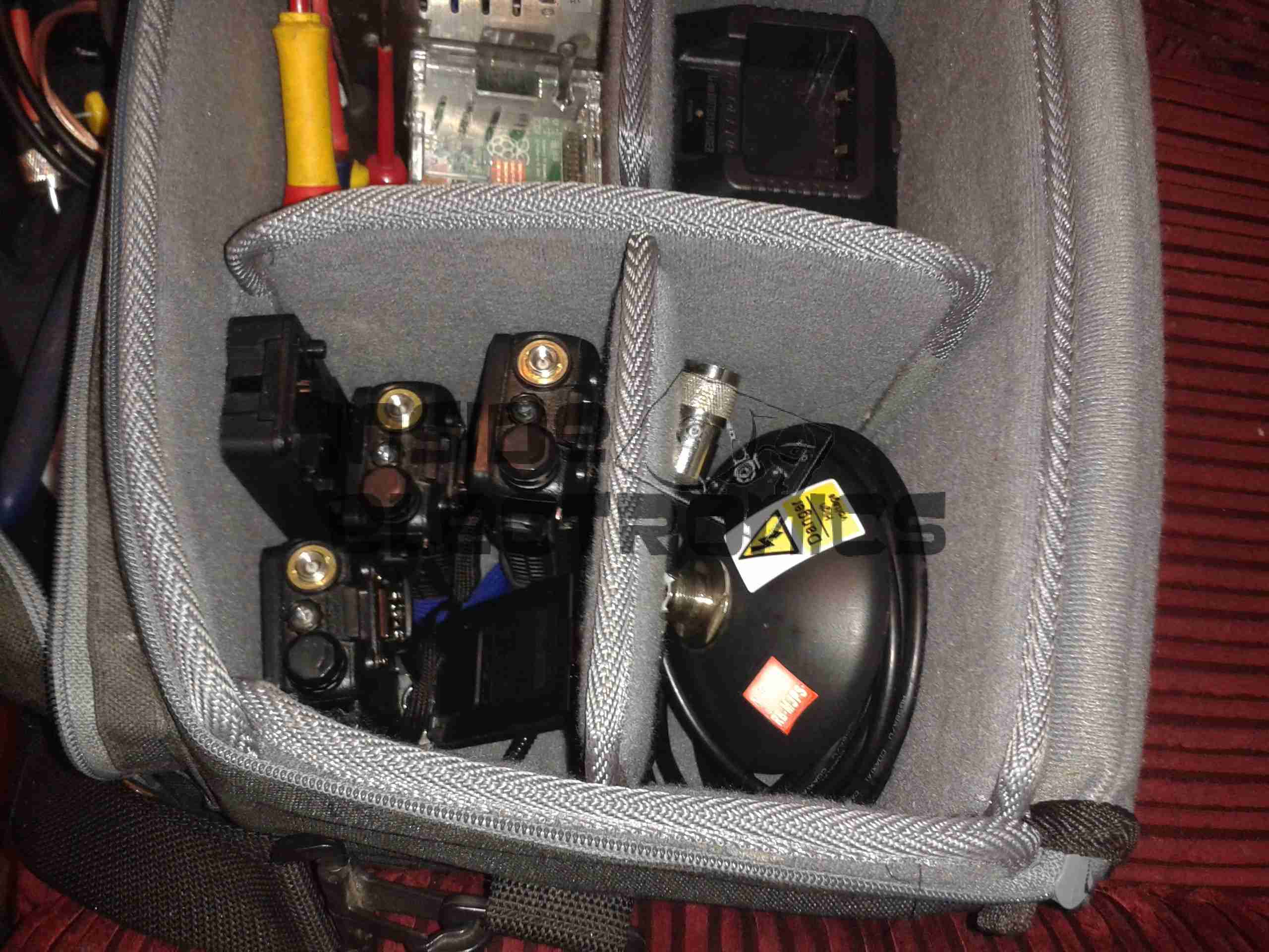
HTs
In the bag I also carry three Baofeng UV-5R handhelds. Extremely useful for short range site communications, along with their charger bases. The charging base on the right has been slightly modified to support charging of my main LED torch as well, which uses similar Li-Ion based packs as the Baofengs.
Baofeng 12v Charger
As the charger bases for the Baofeng HTs take a supply of 10v DC, I have constructed a 12v adaptor system for them. (Which utter prat of an engineer at Baofeng picked 10v?)
Linear Amplifier & SWR Meter
Also included is a small Alinco ELH-2320 35W 2m linear amplifier. This was given to me from the local HackSpace in Manchester. (They don’t have any ham members, besides myself). Also here is my small SWR & Power meter, SDR kit & a pair of syringes. These are filled respectively with Copaslip copper loaded grease, (very good for stopping fasteners exposed to the weather from seizing up), and dielectric silicone grease. (I use this stuff for filling connectors that are exposed to the weather – keeps the water out).
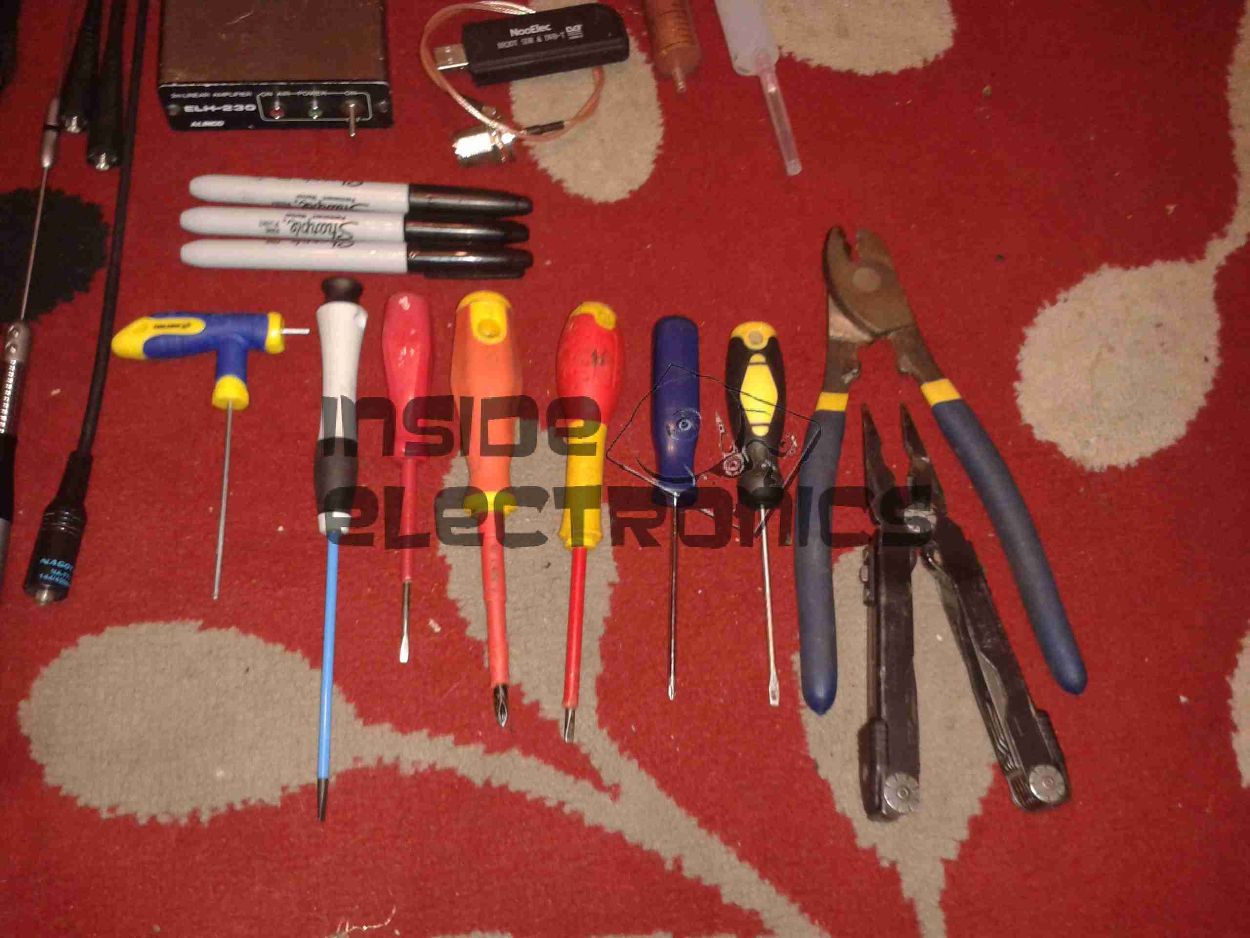
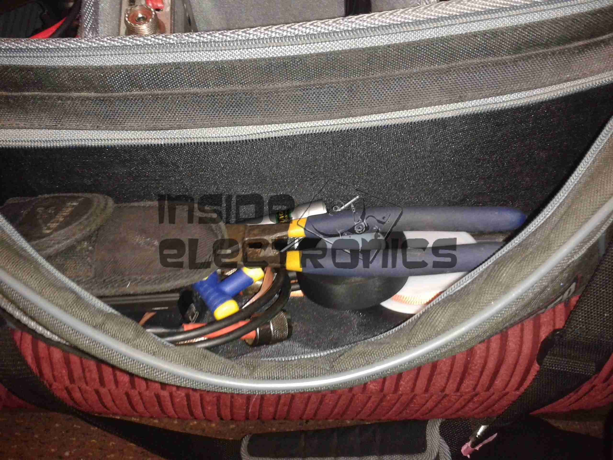
Tools
I always keep essential tools in the bag, here is the small selection of screwdrivers which fit pretty much any screw fastener around, my heavy-duty cable shears (these buggers can cut through starter cable in one go!) and my trusty Gerber Diesel multitool.
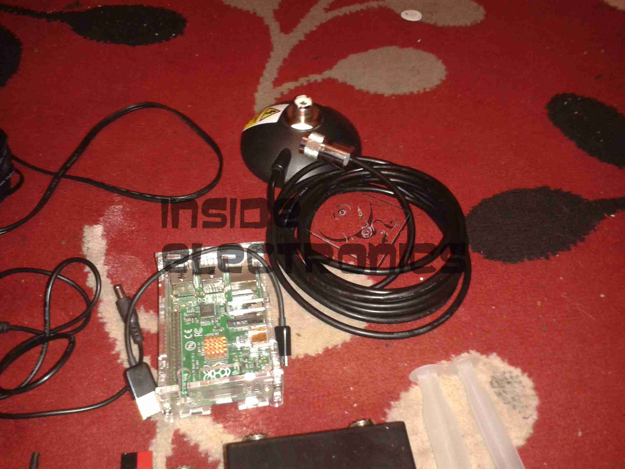
Magmount & Pi
Main antenna magmount & a spare Raspberry Pi.
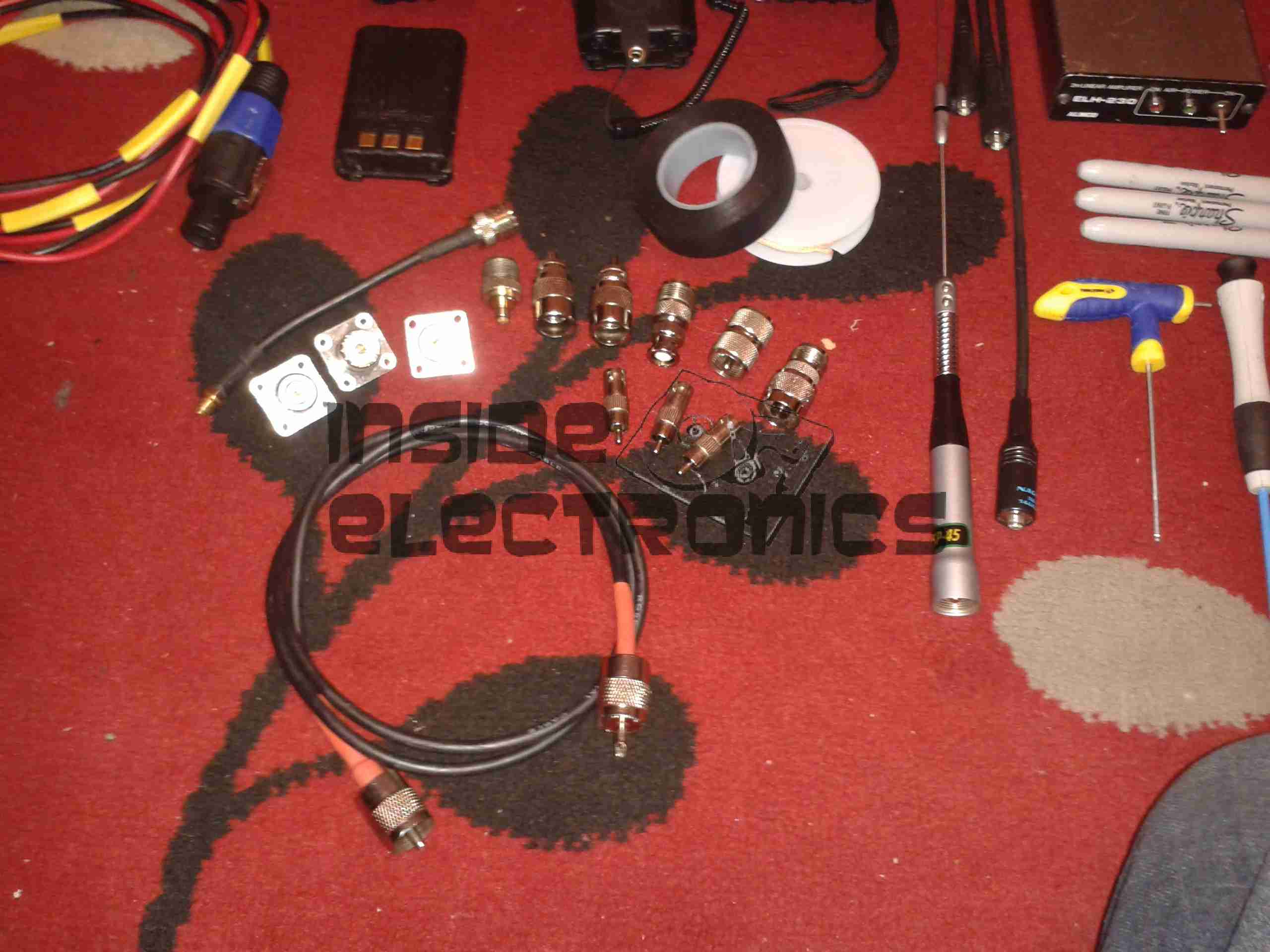
Antenna, Patch Leads, Etc.
Finally, the antennas for the HTs, main dual-band antenna (Nagoya SP-45) for the magmount, a small selection of spare plugs, sockets & adaptors. Also here is a roll of self-amalgamating tape, very handy for waterproofing wiring connections (especially when used in conjunction with the silicone grease), & a roll of solder wick.
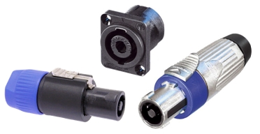
Now, the main power connectors of choice for my equipment are Neutrik SpeakOn type connectors:
Neutrik SpeakOn
These connectors have many advantages:
They are positive locking connectors. No more loose connections.
They have a high continuous current rating of 30A RMS.
Relatively weather resistant.
Also, they have two pairs of pins – and as some of my bigger non-radio related equipment is 24v, this allows me to use a single set of plugs for everything. Without having to worry about plugging a 12v device into a 24v socket, and letting out the magic blue genie.
Once everything is packed up, here’s the bag:
Packed
Everything has a neat little pocket for easy access. Some closeups below.
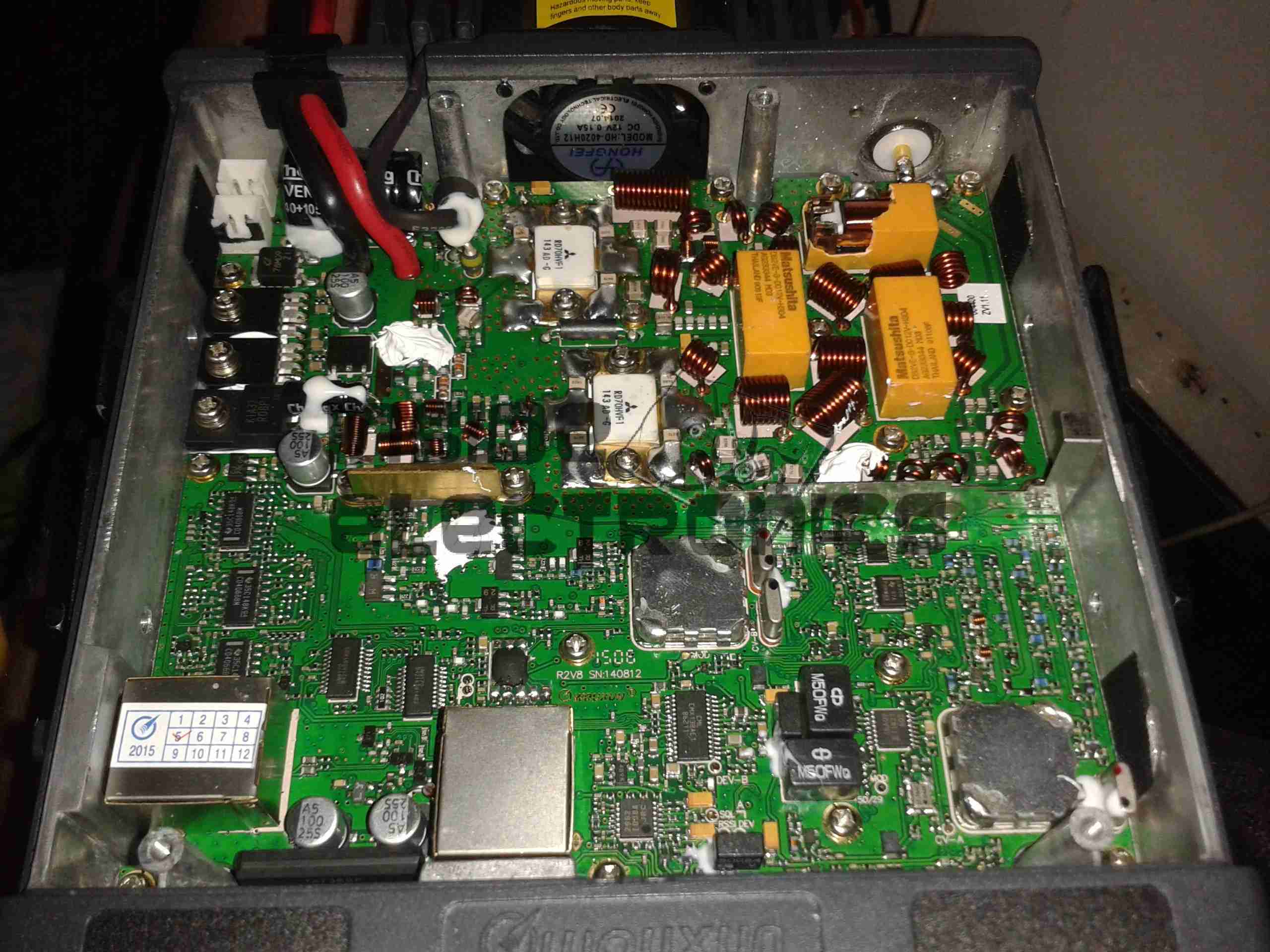
Following on from my review, here are some internal views & detail on the components used in this radio. Below is an overview of the main PCB with the top plate removed from the radio.
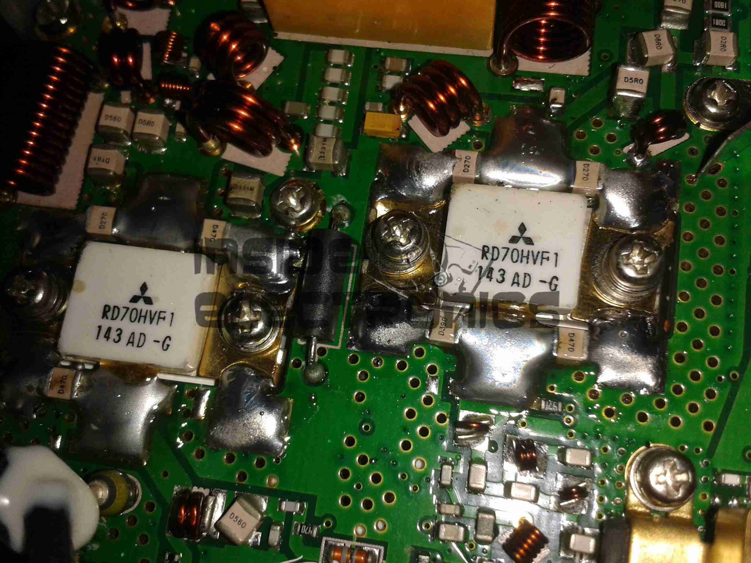
Cover RemovedRF Final Amplifier Stage
Most visible are these MOSFETs, which are Mitsubishi RD70HVF1 VHF/UHF power devices. Rated for a maximum of 75W output power at 12.5v (absolute maximum of 150W, these are used well within their power ratings. They are joined to the PCB with heavy soldering, with bypass caps tacked right on to the leads.
RF Pre Drivers
Here is the RF pre-driver stage, with intermediate transistors hidden under the small brass heatspreader.
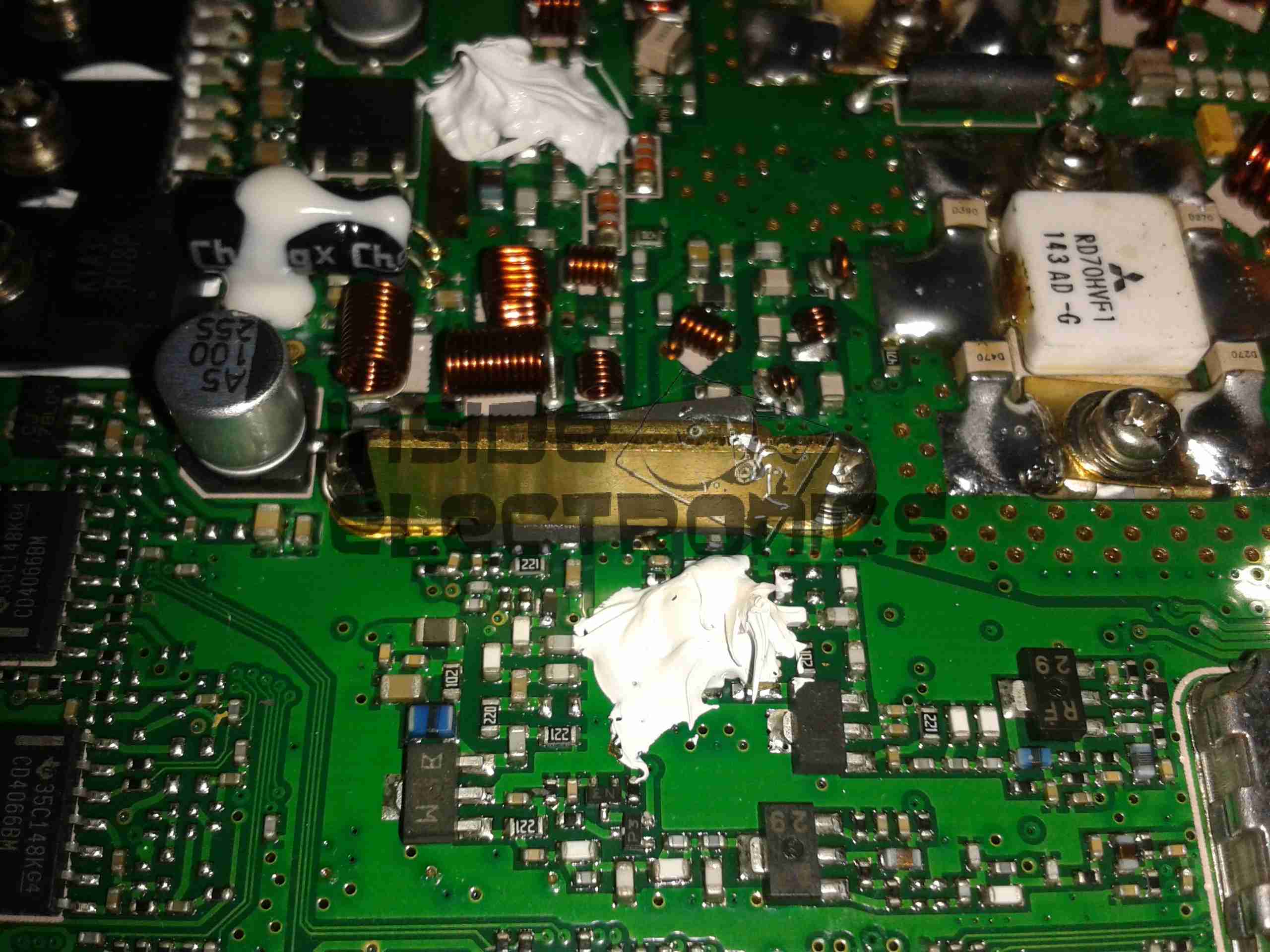
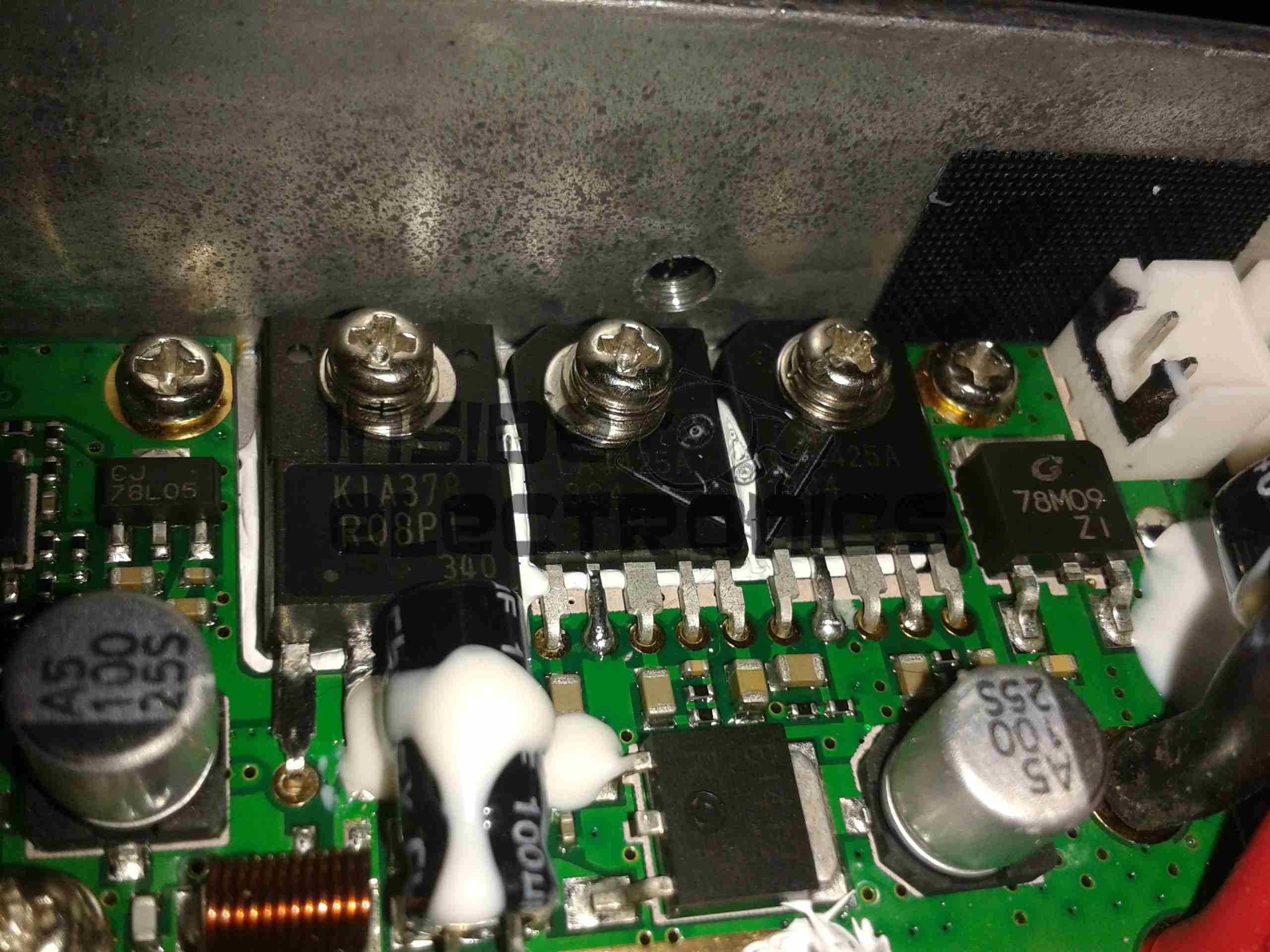
Power Section
In the top left corner of the radio, near the power input leads, is the power supply & audio amplifier section. Clearly visible are the pair of LA4425A 5W audio power amplifier ICs, these drive the speakers on the top of the radio. Either side of these parts are a 7809 & a 7805 – both linear regulators providing +9v & +5v logic supplies respectively. The large TO220 package device is a KIA378R08PI 3A LDO regulator with ON/OFF control, this one outputs +8v. Just visible in the top right corner are the sockets for the speaker connections.
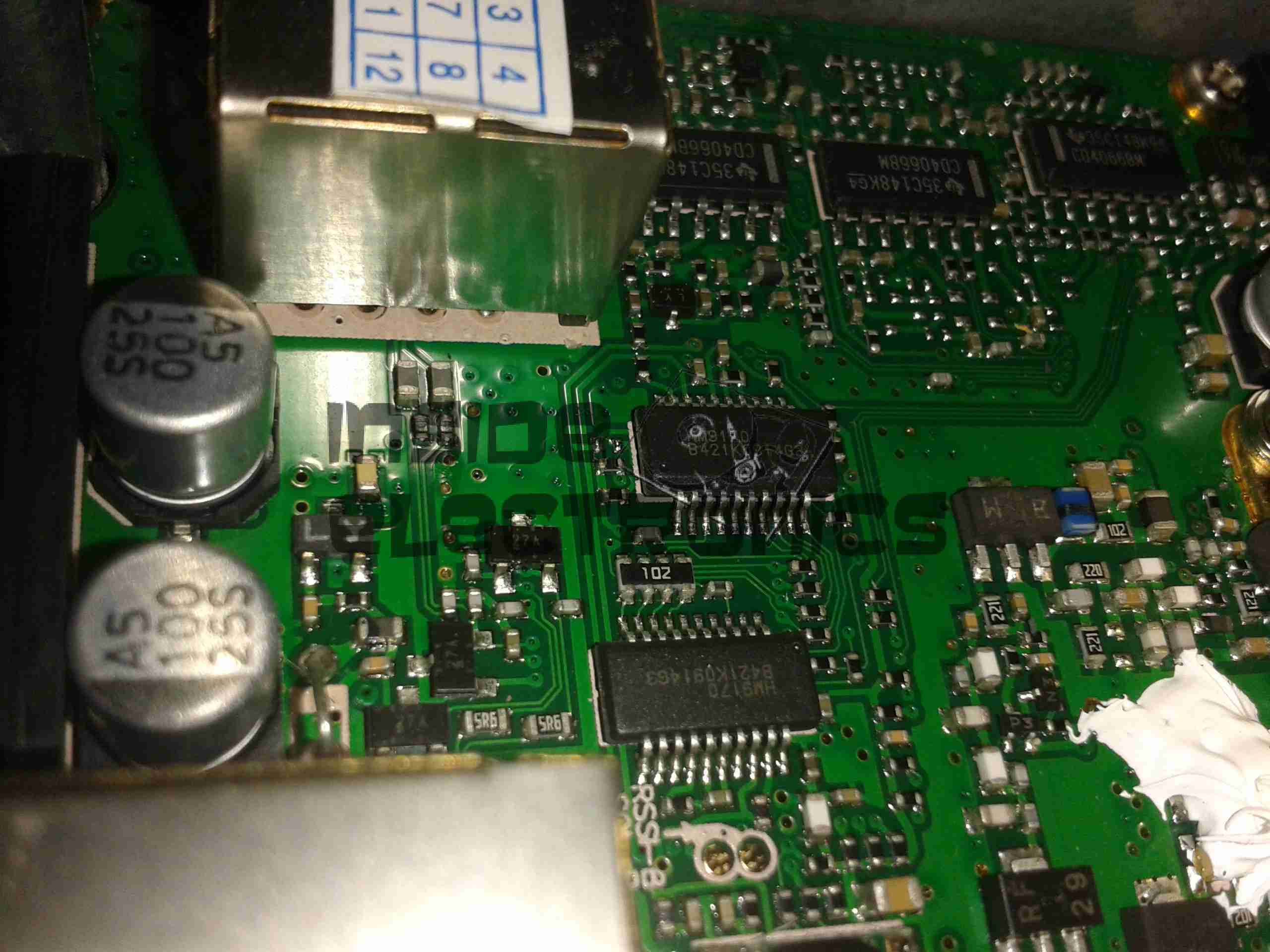
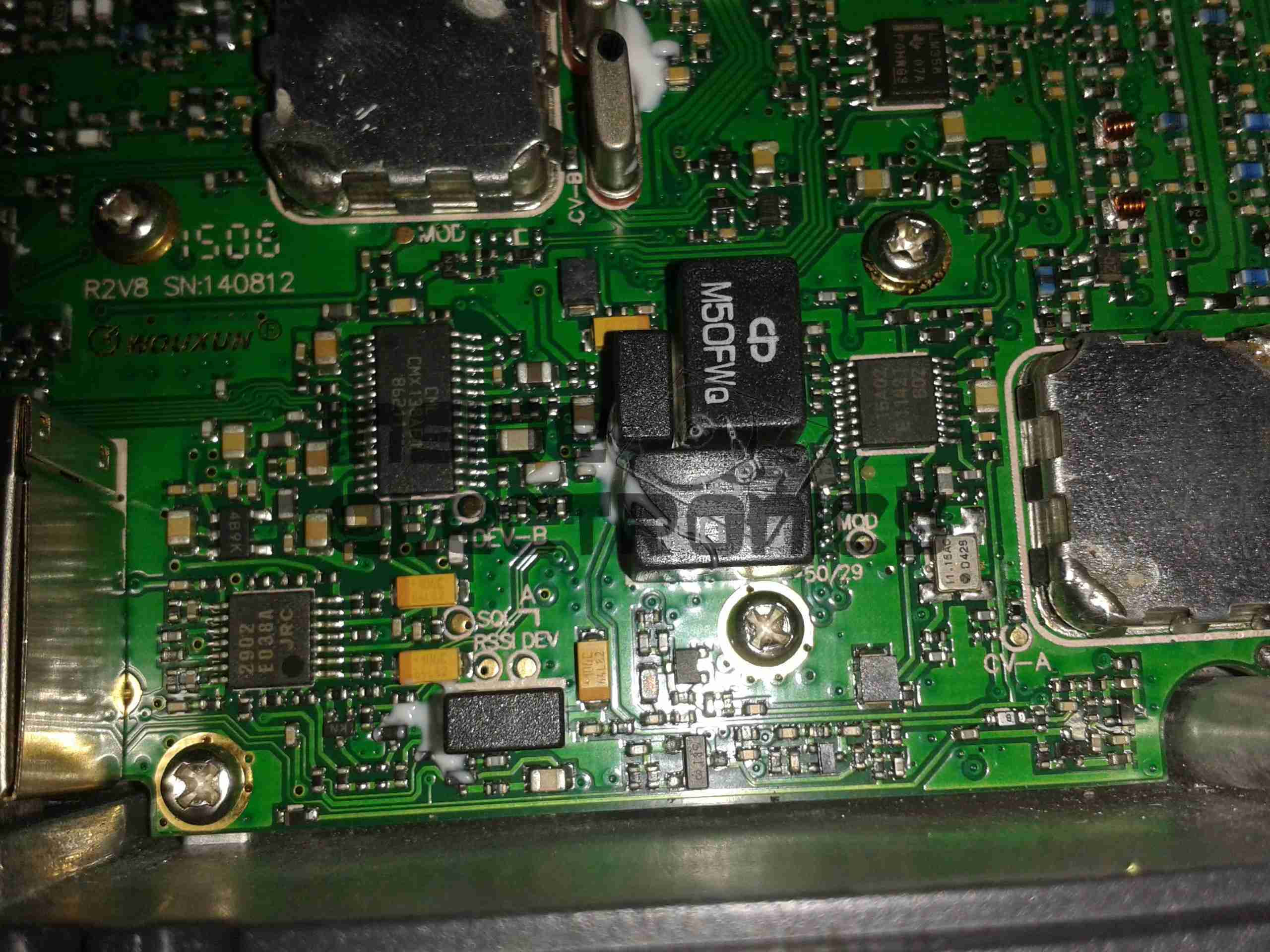
DTMF Circuits
Here are the two ICs for dealing with DTMF tones, they are HM9170 receivers.
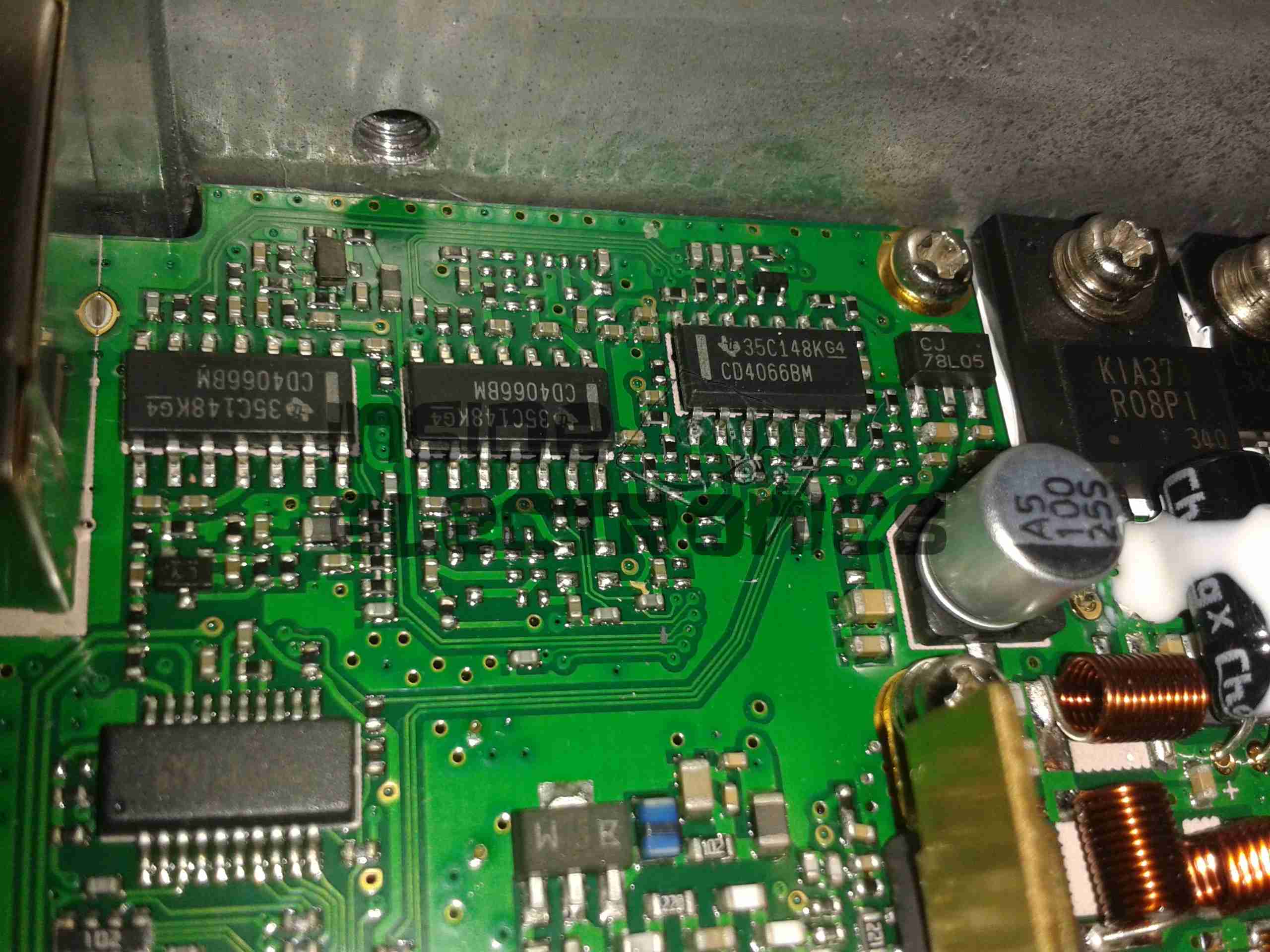
Glue Logic
In the corner next to the interface jack, there are some CD4066B Quad Bilateral switches. These make sense since the interface jack has more than a single purpose, these will switch signals depending on what is connected.
RF Section
Here are visible the RF cans for the oscillators, the crystals visible next to the can at the top. The shields are soldered on, so no opening these unfortunately.
Also visible in this image is a CMX138A Audio Scrambler & Sub-Audio Signalling processor. This IC deals with the Voice Inversion Scrambling feature of the radio, & processes the incoming audio before being sent to the modulator.
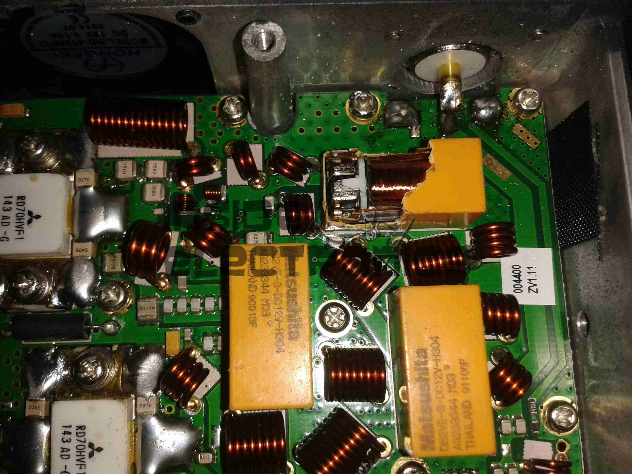
Output Filter Network
Shown here is the RF output filter network, this radio uses relays for switching instead of PIN diodes, I imagine for cost reasons. The relay closest to the RF output socket has had a slight accident 🙂 This is slated to be replaced soon.
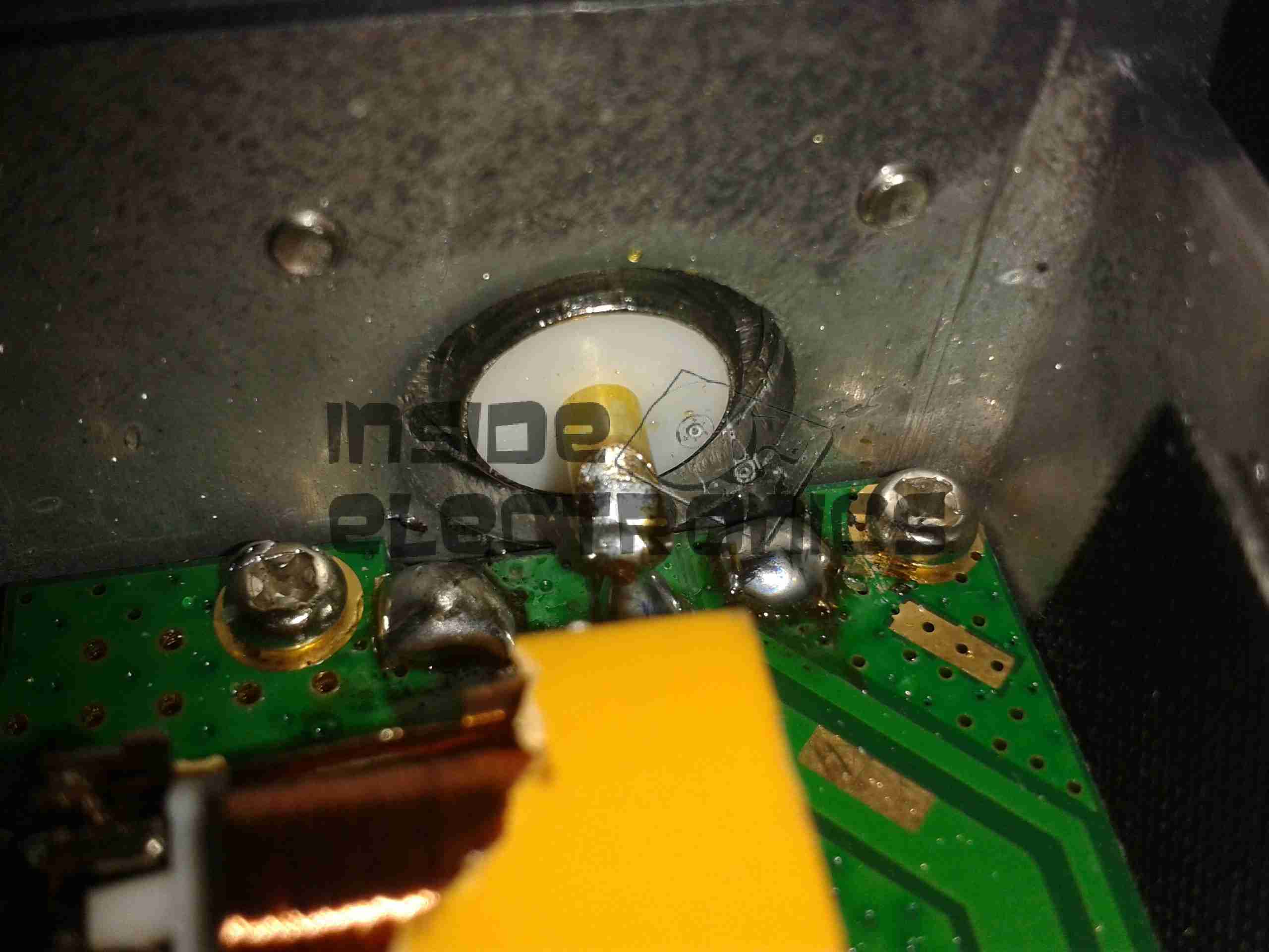
RF Output Jack
Finally, the RF output jack.
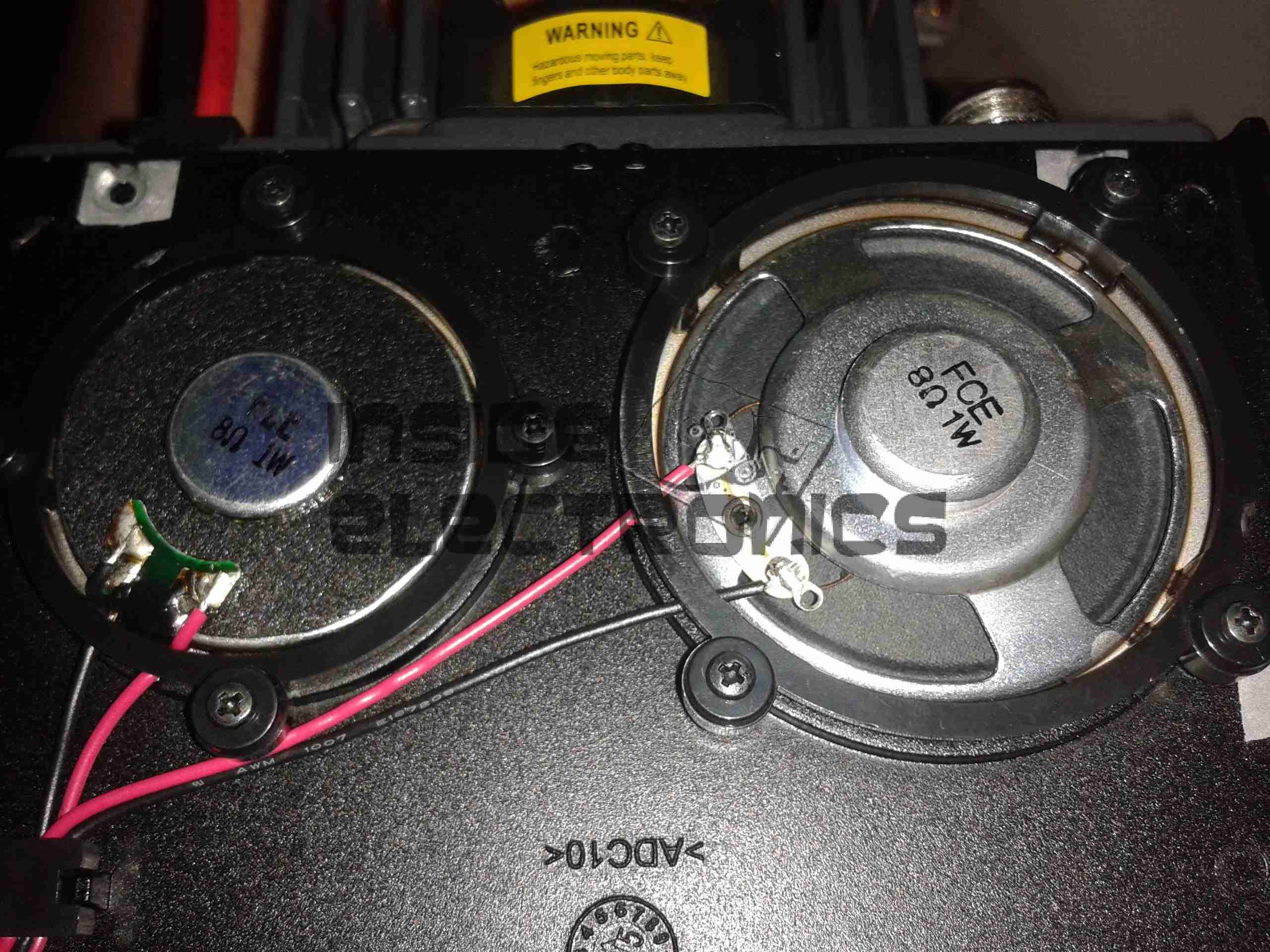
Audio Speakers
Here the speakers are shown, attached to the bottom of the top plate. They are both rated 8Ω 1W.
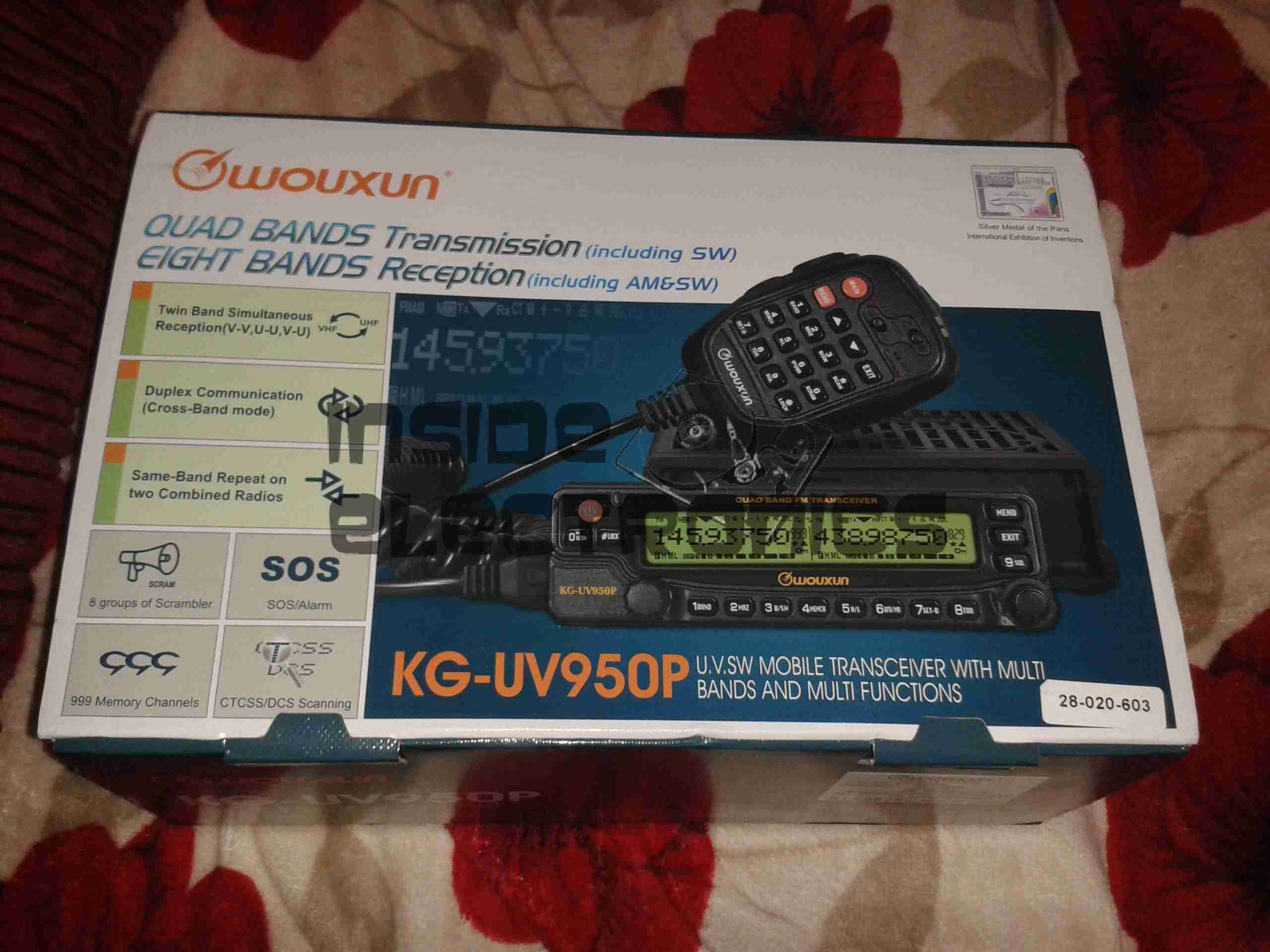
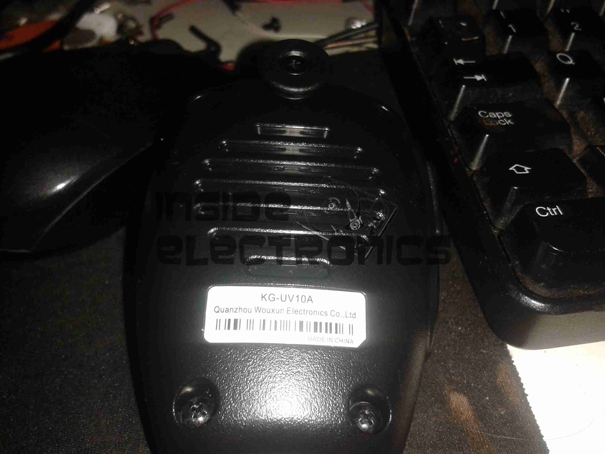
After running on handies for all of my Ameteur Radio life, I figured it was time for a new radio, this time a base station/mobile rig, & after some looking around I decided on the Wouxun KG-UV950P.
Shown below is the radio as delivered:
Wouxun Boxed
This radio has the capability to transmit quad-band, on 6m, 10m, 2m & 70cm. It also has the capability to receive on no fewer than eight bands. Also included in the feature set is airband receive, & broadcast FM receive.
TX power is up to 50W on 2m, 40W on 70cm, & 10W on 6m/10m.
Opened
For once with a Chinese piece of electronic equipment, the manual is very well printed, and in very good English.
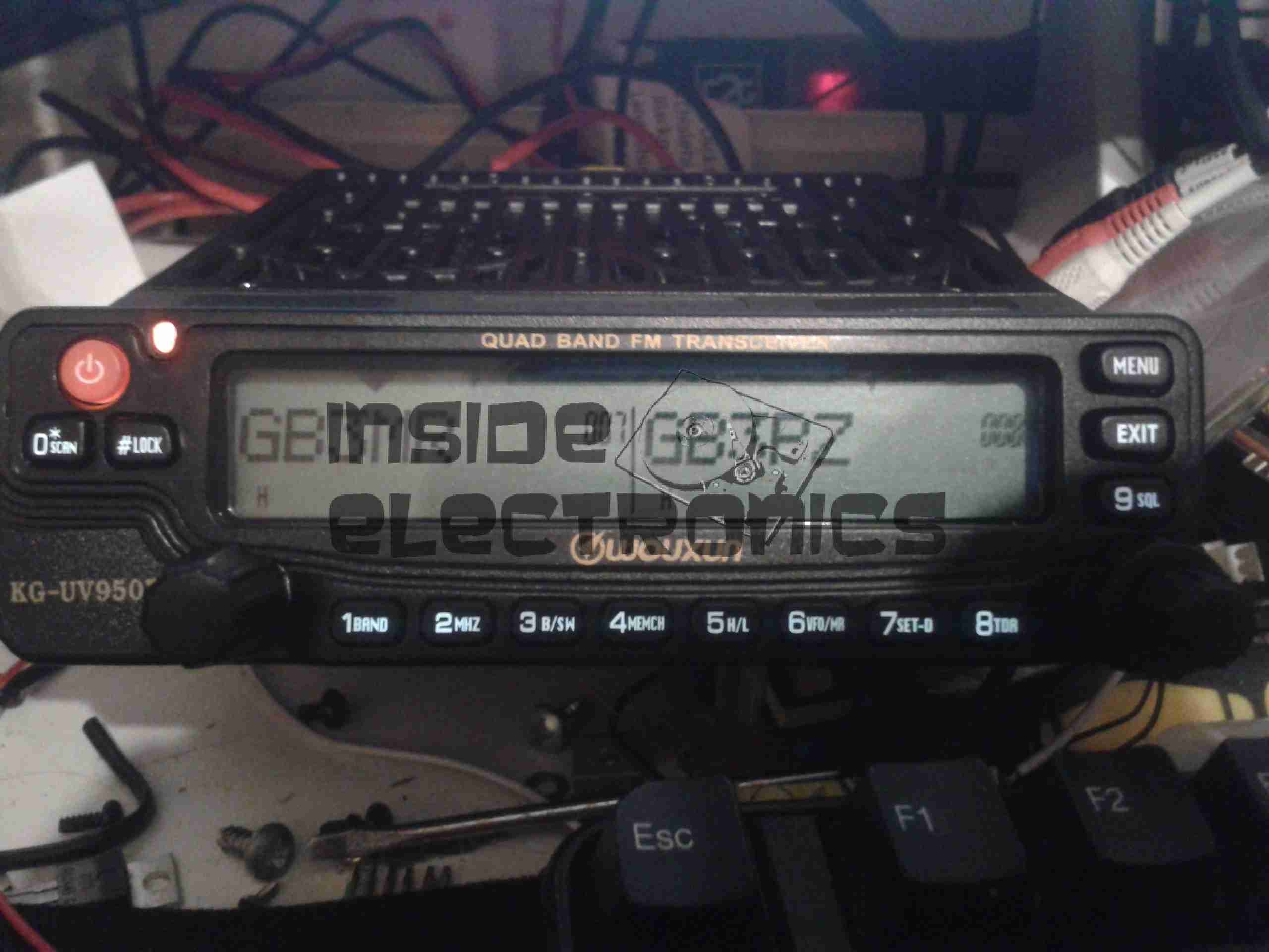
Radio Operating
Here is the radio in operation, connected to my 65A 12v power supply. I have the radio set here monitoring a couple of the local 70cm repeaters.
The display is nice & large – easy to see at a glance which station you’re tuned to. The backlight is also software settable to different colours.
Status indicators on the top edge of the display can be a bit difficult to see unless the panel is directly facing the user though, not to mention that they are rather small.
This radio is true dual-watch, in that both VFOs can be receiving at the same time, this is effected by a pair of speakers on the top panel:
Speakers
The left VFO speaker is smaller than the right, so the sound levels differ slightly, but overall sound quality is excellent. There is also provision on the back of the unit to connect external speakers.
The dual volume controls on the right hand bottom corner of the control panel are fairly decent, if a little twitchy at times. There is also a fair amount of distortion on the audio at the higher volume levels.
The controls themselves are potentiometers, but the controller appears to read the setpoint with an ADC – this means that if the control is set to just the right point, the selected level will jump around on the display & never settle down.
The radio itself is built from a solid aluminium casting, mostly for heatsinking of the main RF output stage MOSFETs. This gives the radio a very rugged construction.
A small fan is provided on the rear for cooling when required. This can be set in software to either be constantly running, (it’s pretty much silent, so this is advantageous), or only run when in TX mode. The fan will also automatically come on when a high internal temperature is detected.
Hand Mic
Here is the microphone. Like the main unit of the radio this is also very solidly built, fits nicely in the hand & the PTT has a nice easy action, which helps to prevent straining hands while keeping the TX keyed.
Conveniently, all of the controls required to operate the radio are duplicated on this mic, along with a control lock switch, & backlighting for the buttons.
Another Speaker
Another output speaker is placed in the back of the mic. This one can be activated through the menu system, to either use the main body speakers, the mic mounted one, or both.
A mounting hook for the mic is provided to attach to any convenient surface.
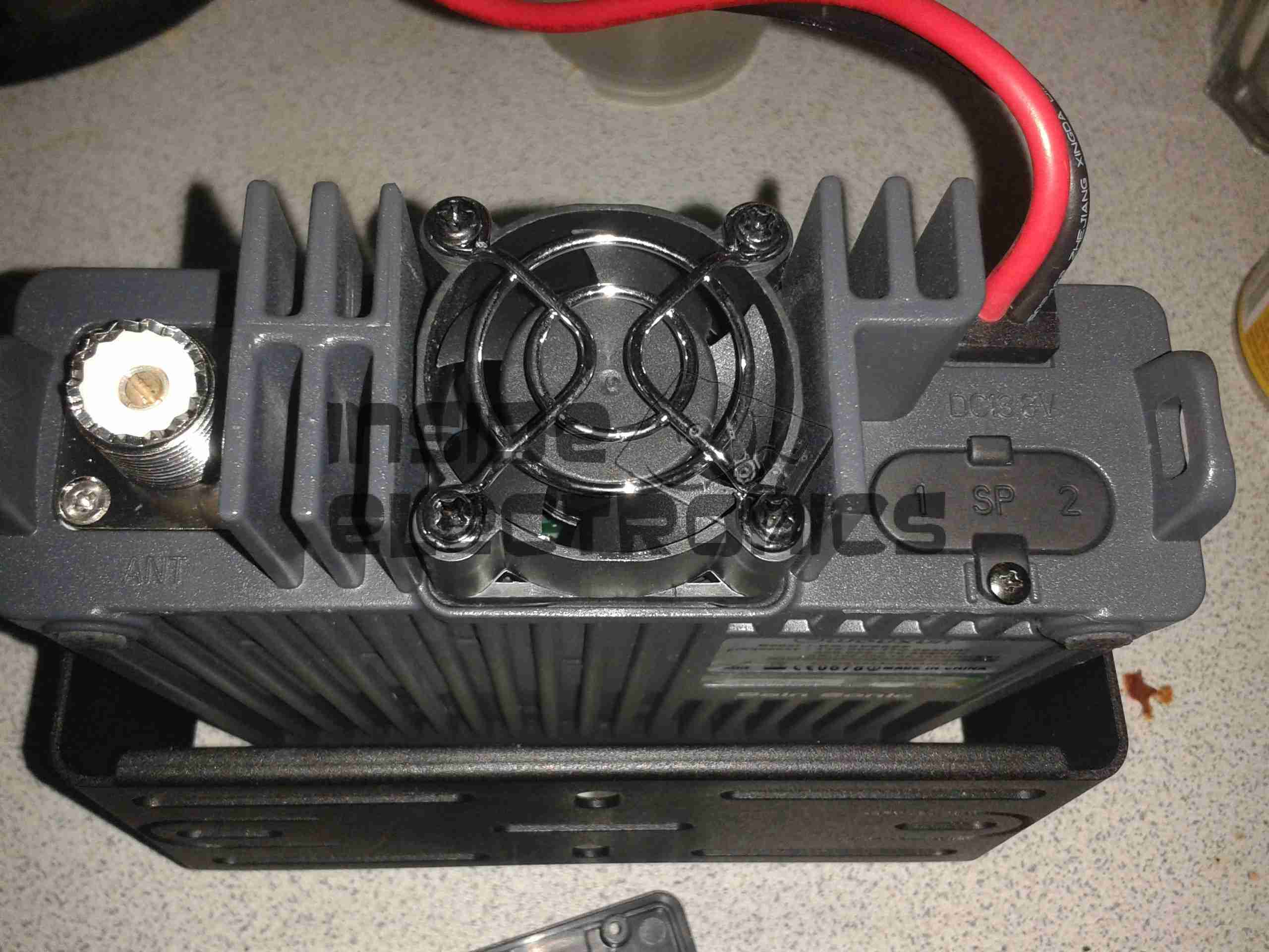
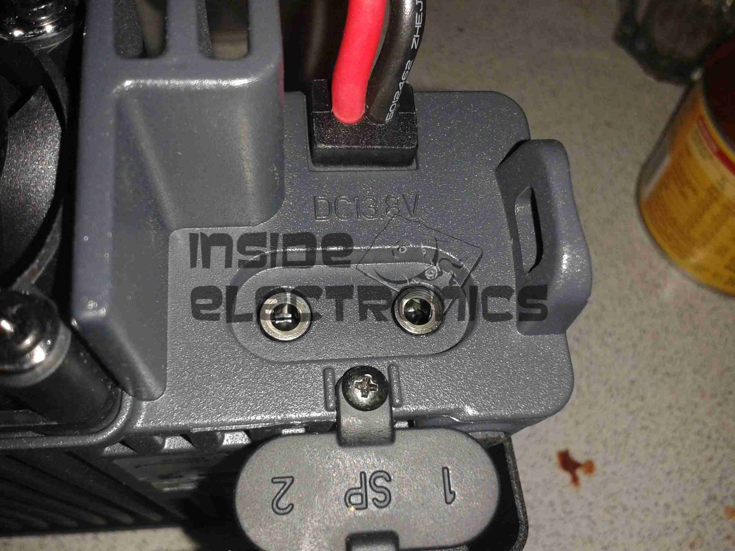
Radio Back
Here’s the back of the radio, with some of the big heatsink fins, the fan in the centre. To the left is the PL259 RF output, this looks to be a high quality Teflon insulated one. On the right are the power input leads & the external speaker outputs.
External Speaker Sockets
The external speaker connections are via 3.5mm jacks. I haven’t yet tested this feature.
Remote Mounting Plate
The control panel of this radio is detachable from the main body, and a pair of adaptors are provided. This either allows the radio display to be angled upwards toward the user, set parallel, or even mounted remotely. A control extension cable is provided to allow the main body to be mounted a fair distance away.
External Interface Connectors
On the left of the radio is the PC control & programming port, & the mic connector. Wouxun *really* like RJ-45 connectors, they’ve used them for everything on this radio.
Also visible here is the tilted faceplate adaptor.
The supplied software to program the radio, while functional, is absolutely horrific. Hopefully someone will add support for this radio into CHIRP. Anything would be an improvement in this area.
Everything considered, I like this radio. It’s very solidly built, easy to use, and sounds brilliant.
TX audio is great, (or so my other contacts tell me).
Unsurprisingly, the unit gets warm while transmitting, however on high power, it does get uncomfortably warm, and the built in fan does little in the way of helping when a long QSO is in progress. I may remedy this at some stage with a more powerful fan. A little more airflow would do wonders.
If the programming software was built as well as the radio, I’d have zero serious complaints.
At full power, the radio pulls ~10A from the power supply, at 12.9v DC.
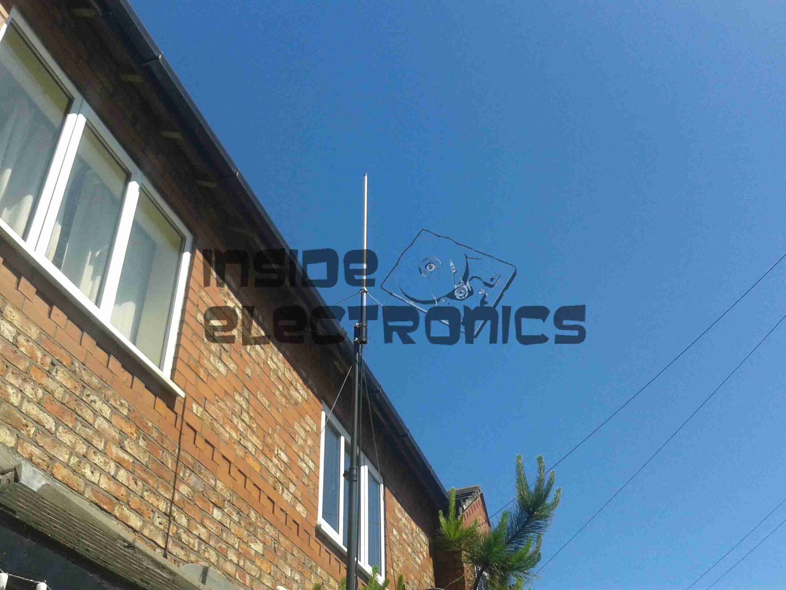
As for the antenna I’m currently using, it’s a Diamond X30, mounted on a modified PA speaker stand, at ~30 feet above ground. The feeder is high quality RG-213.
TX Antenna
When I manage to get the set disconnected, a partial teardown will be posted, with some intimate details about the internals. Stay tuned!
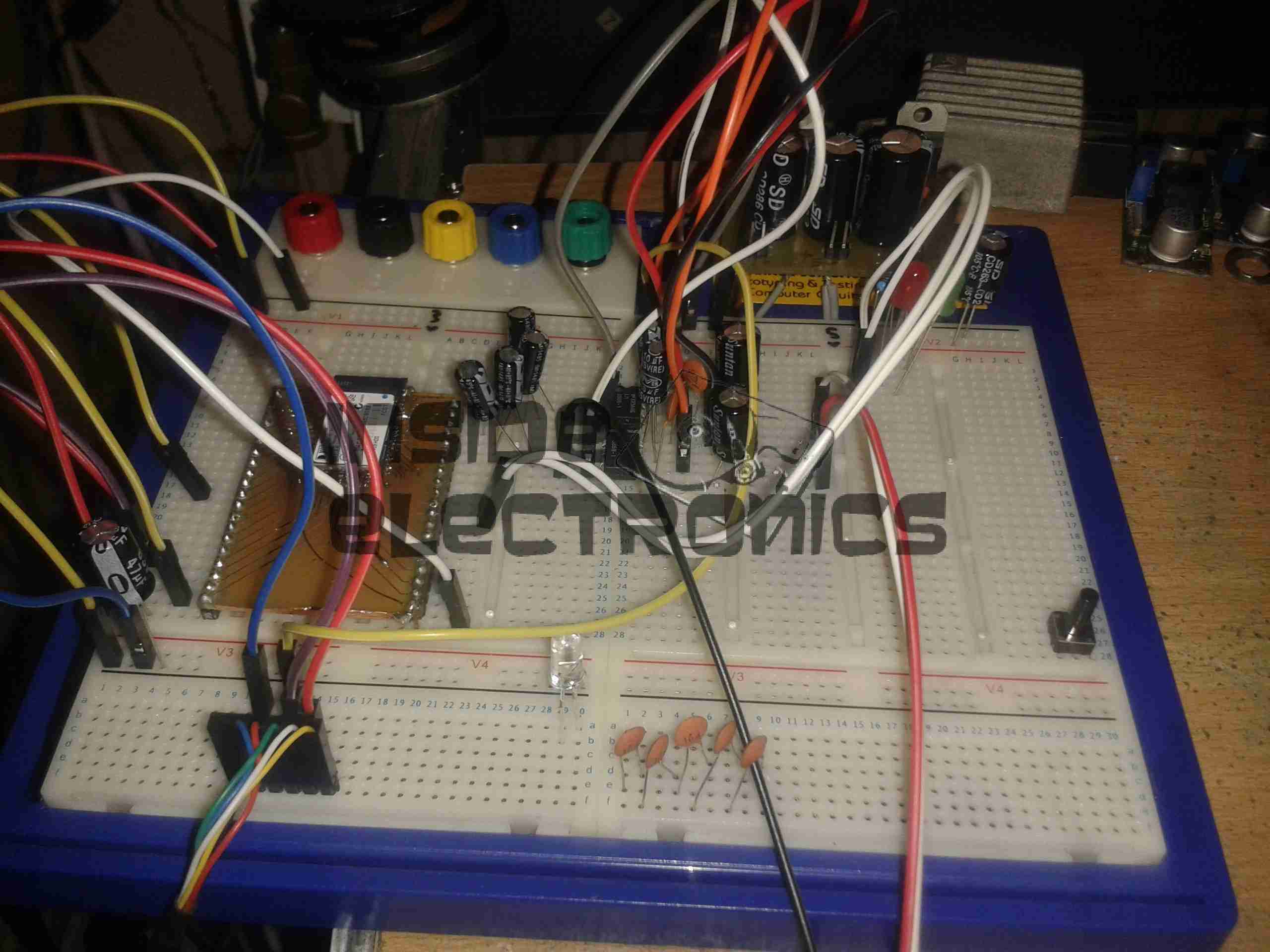
I’ve been doing some tinkering with the RN-52 Bluetooth Audio module from Roving Networks, in prep for building a portable wireless speaker system, & thought I’d share my designs.
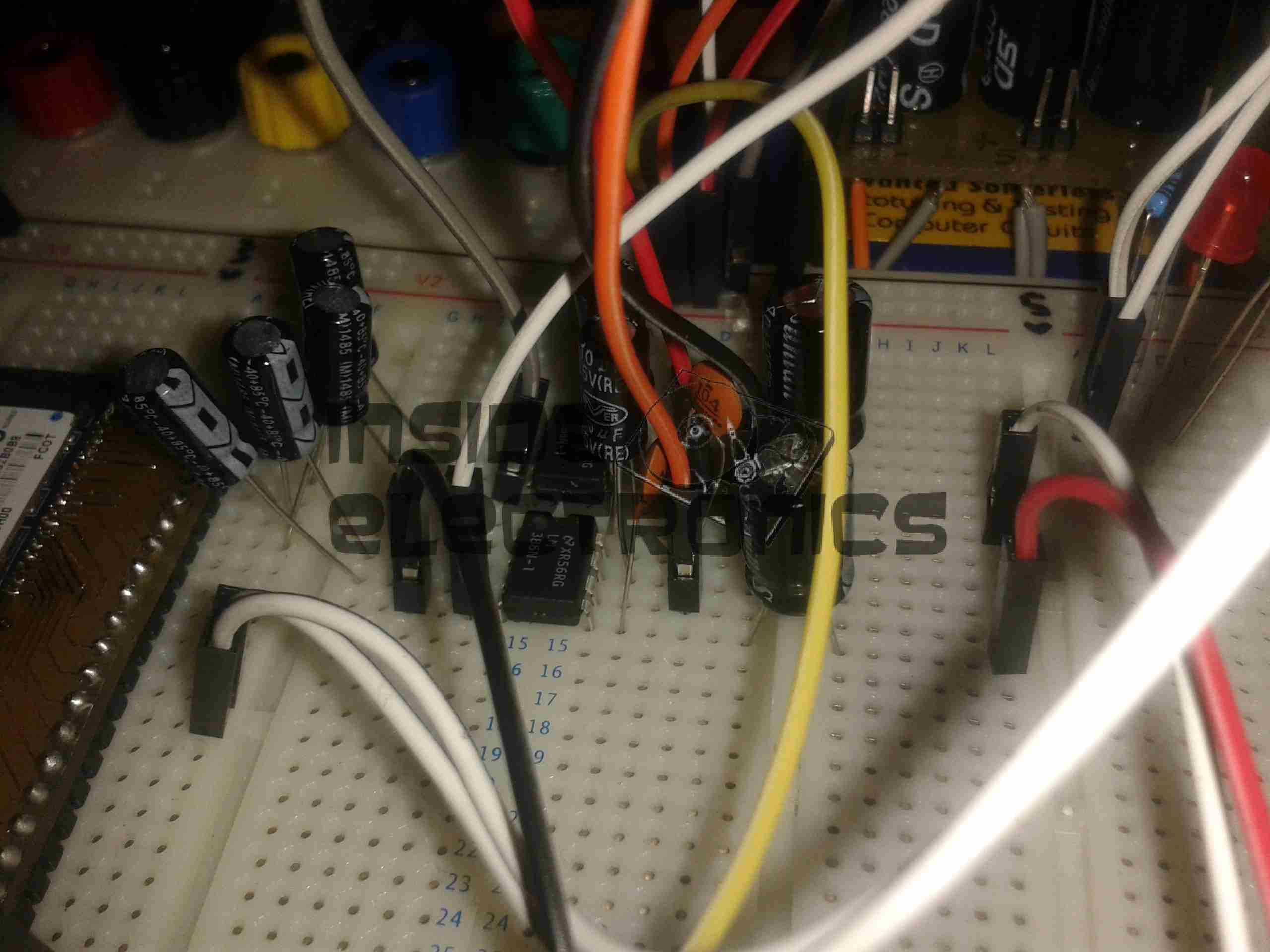
Initially I was having some issues with RF noise on the audio output from the RN-52, as I was only using the outputs single-ended. The module didn’t like this treatment, with all the RF whine coming straight out of the speakers.
To fix this issue I have used a pair of jellybean LM386 audio power amplifiers, running in differential input mode. This solves the high-pitched whine when the audio is enabled, & also allows the module to directly drive a set of 32Ω headphones at a reasonable level.
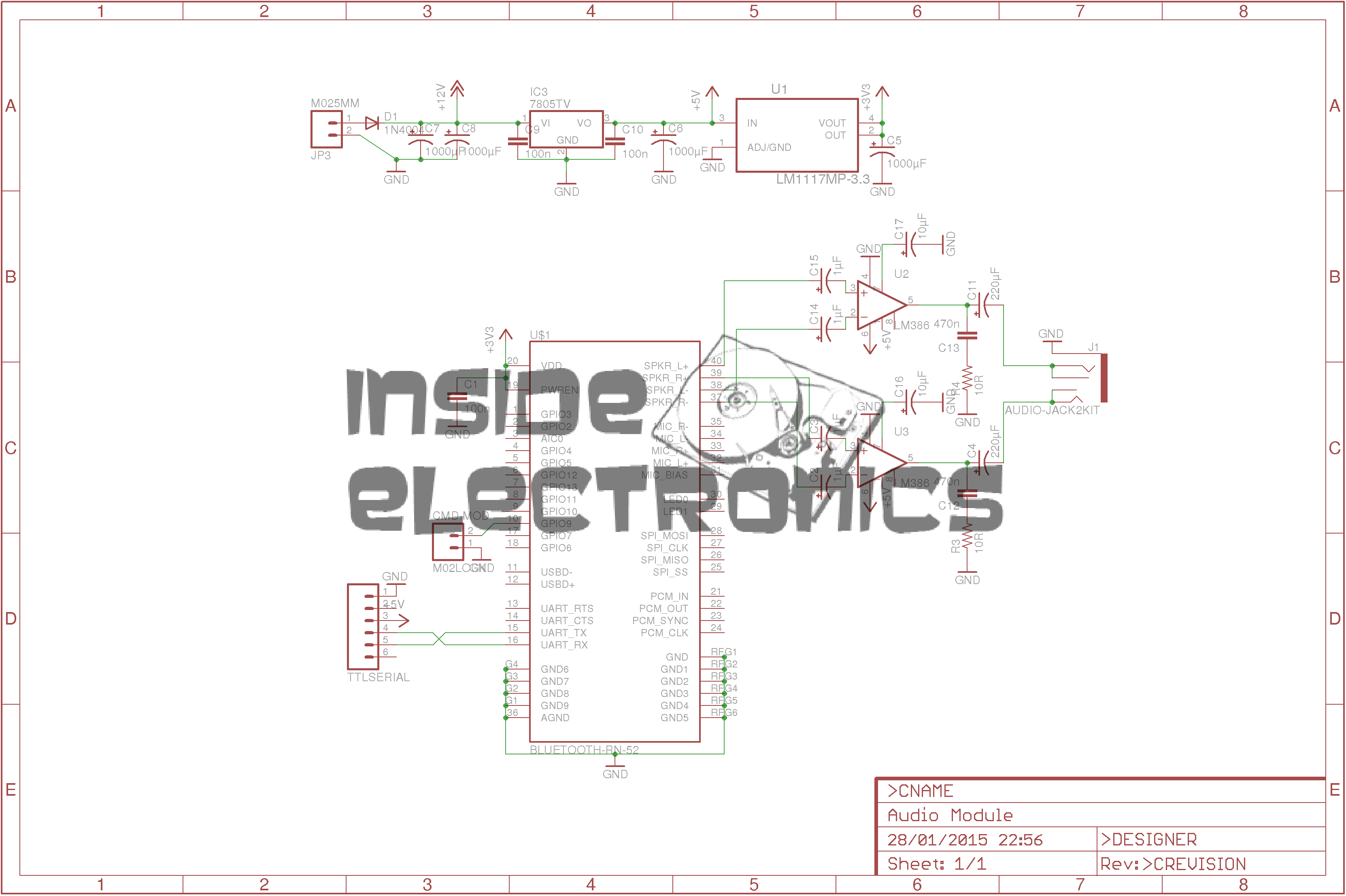
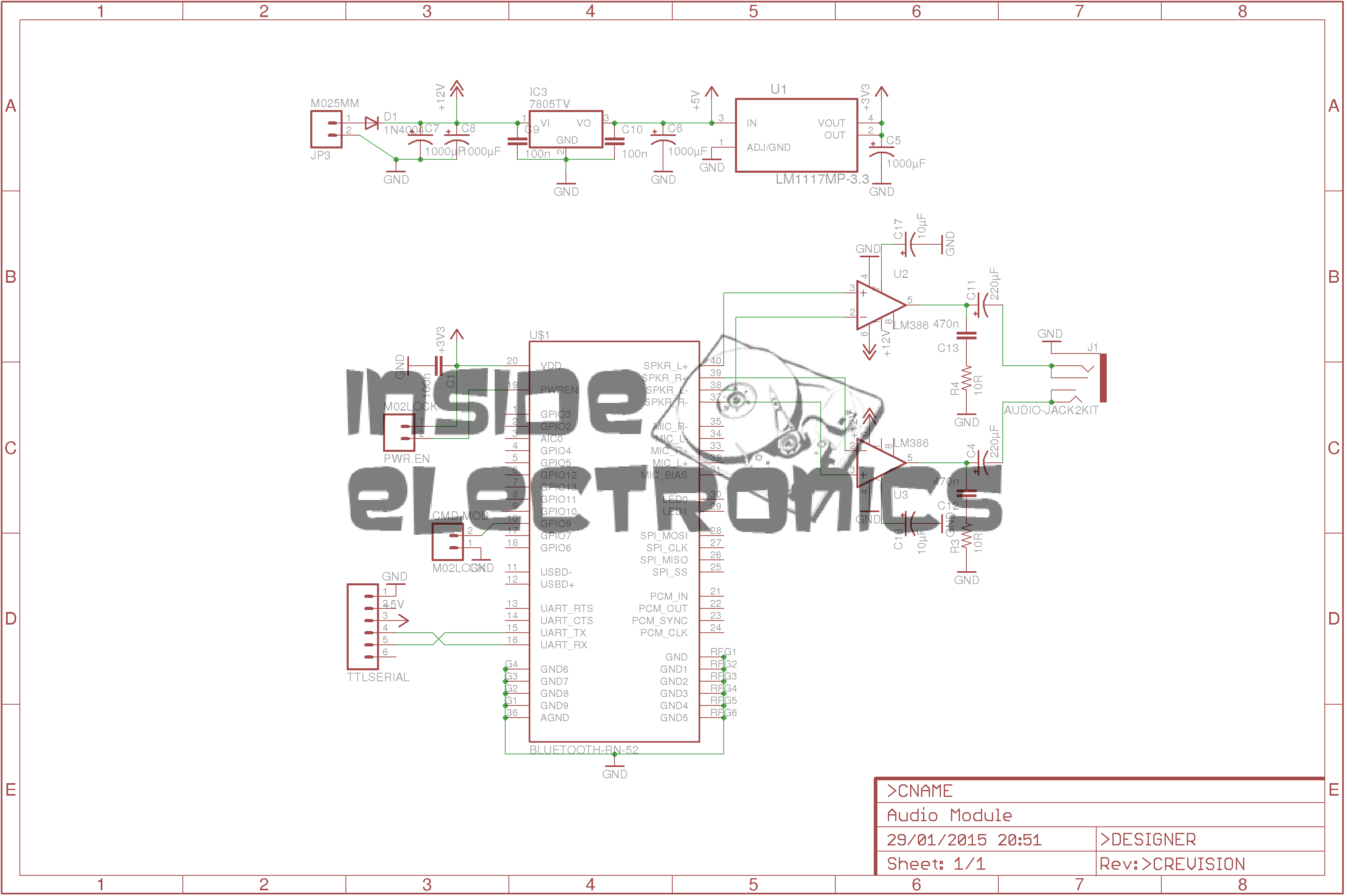
In Eagle I have designed a simple board, routing only the audio output, serial TTL & command mode pins out, along with the supporting power supply circuitry to operate from 12v DC.
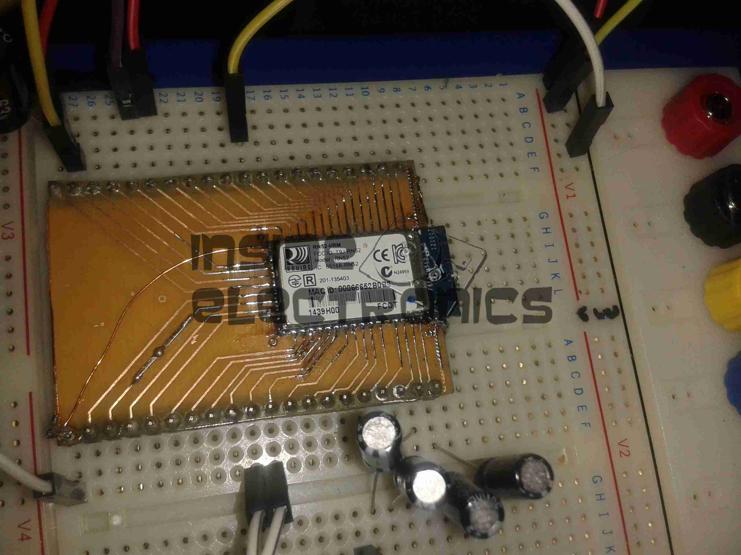
RN-52 Breadboard
Above is the current incarnation of the circuit on the breadboard. The RN-52 is on the left, audio power stage in the centre & headphone output on the right.
RN-52 Breakout
The bluetooth module on a breakout board. I was cheap in this case & etched my own board. I’m not paying Sparkfun, (as much as I like them), an extra ~£10 for a small PCB with the pins broken out. Much cheaper to spend 15 minutes with the laser printer & the iron, & do a toner transfer PCB.
As this board is single sided, I added a ground plane on the underside with copper foil, to help with the RF issues. Breadboards really aren’t all that good at rejecting noise induced when there’s a 2.4GHz transceiver mounted on them.
LM386 Amplifier
The LM386 audio power stage. The differential inputs from the module are capacitively coupled with 1µF electrolytics. This setup remarkably reduced the noise on the output. I left these at their default gain of 20, as I’ll be connecting another high power amplifier stage to drive large speakers.
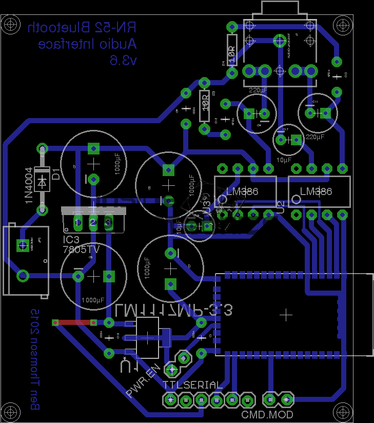
RN-52 Eagle Layout
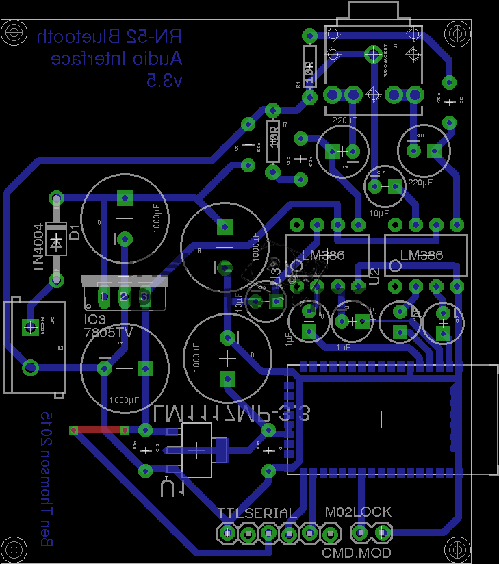
Here’s the circuit laid out in Eagle, ready for PCB.
RN-52 Eagle PCB
And here’s the PCB layout. Only one link required for the +5v line from the TTL serial port.
As always, the Eagle PCB & Schematic layout files are available at the bottom of the article.
*Update 29-01-15*
Rerouted a few things:
Moved the audio power stage to the +12v rail to improve sound response. – As the LM386 has a max input voltage of 12v (absolute maximum 15v), a regulated supply is recommended. The LM386-N4 variant has a higher voltage range, up to 18v. This should be suitable for an unregulated supply.
Removed 1µF coupling capacitors to reduce distortion & amplifier hiss. The capacitors appeared to cause some instability on the amplifier, causing random distortion. Removing them has cured this. No signal hiss has also been reduced to a very low level.
Reversed input polarity on input of one of the amplifiers – this appears to produce better audio.
Added PWR.EN header to allow connection of power button. Saves hassle of cycling power to the board when the RN-52 goes into sleep mode.
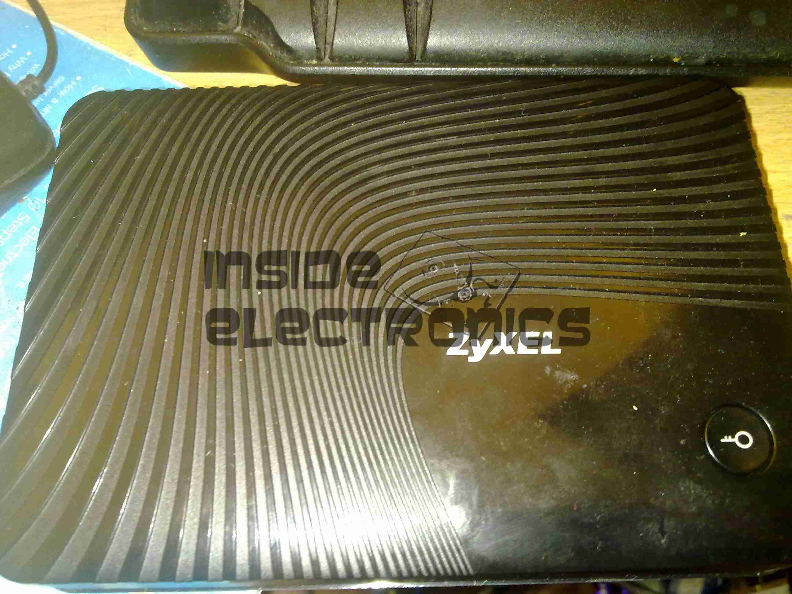
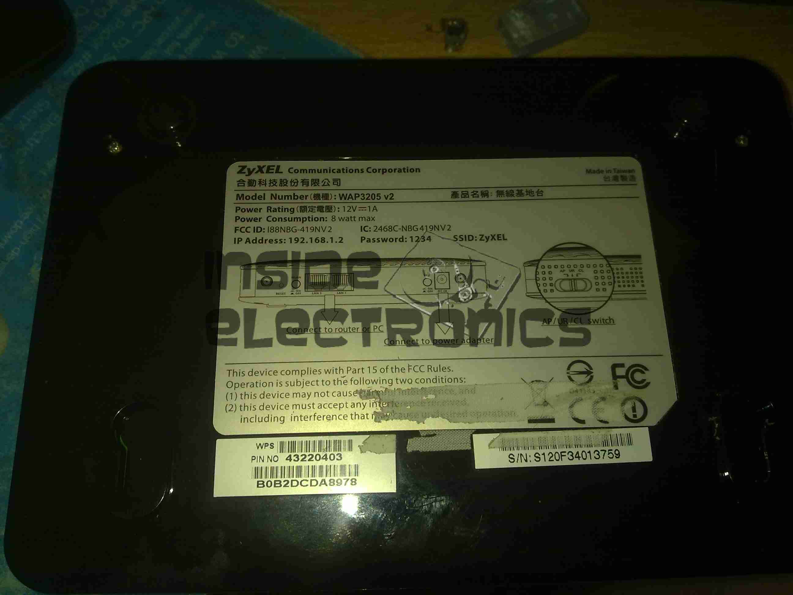
Here is a ZyXel WAP3205 WiFi Access Point that has suffered a reverse polarity event, due to an incorrect power supply being used with the unit.
ZyXEL WAP3205
While most electronic gadgets are protected against reverse polarity with a blocking diode, this unit certainly wasn’t. Applying +12v DC the wrong way round resulted in this:
Blown Switchmode IC (Fuzzy Focus)
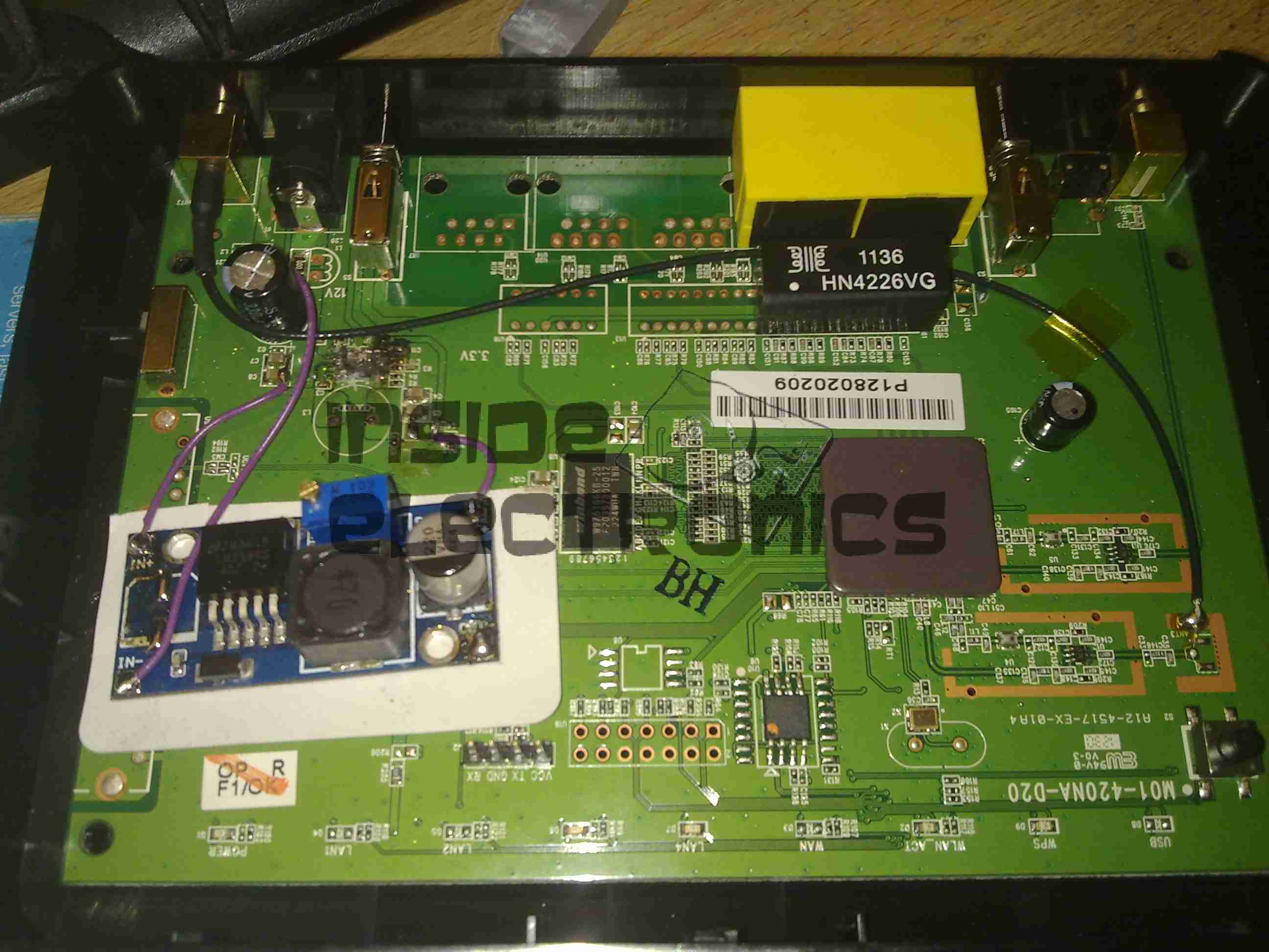
That is the remains of the 3.3v regulator IC, blown to smithereens & it even attempted an arson attack. Luckily this was the only damaged component, & I was able to repair the unit by replacing the switching IC with a standalone regulator. (Replacing the IC would have been preferable, if there was anything left of it to obtain a part number from).
I scraped away the pins of the IC to clear the short on the input supply, removed the switching inductor, & tacked on an adjustable regulator module set to 3.3v. Luckily the voltage of the supply is handily marked on the PCB next to the circuit.
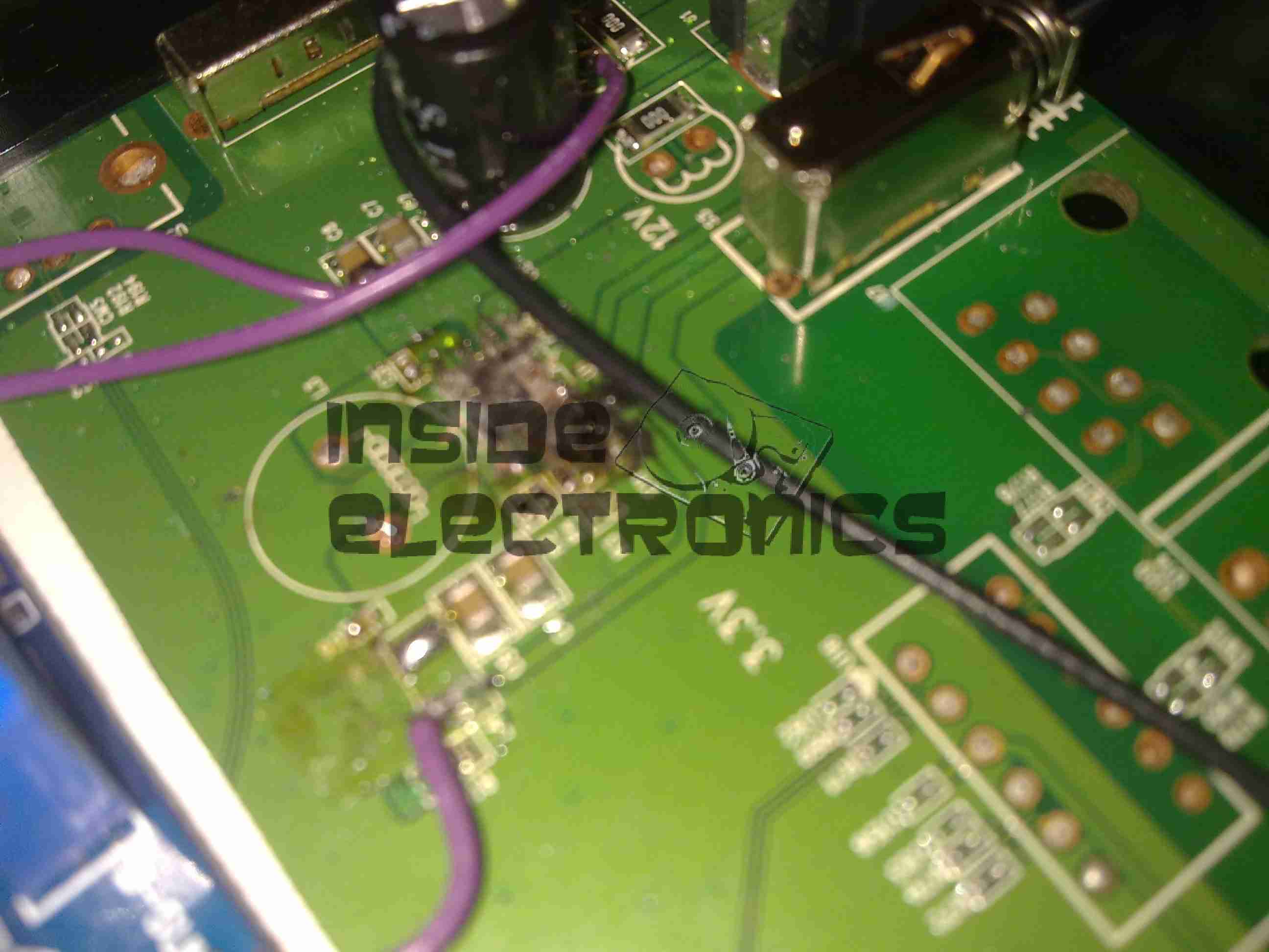
Replacement PSU
Replacement SMPS in place on top of the PCB. The output of the supply is connected to one of the pads of L4 (on my unit just an 0 ohm link), the +12v input is connected to the + rail side of C8 & C7 & the final ground connection is hooked in to the back of the barrel jack.
After this replacement, the unit booted straight up as if nothing had happened. All the logic is undamaged!
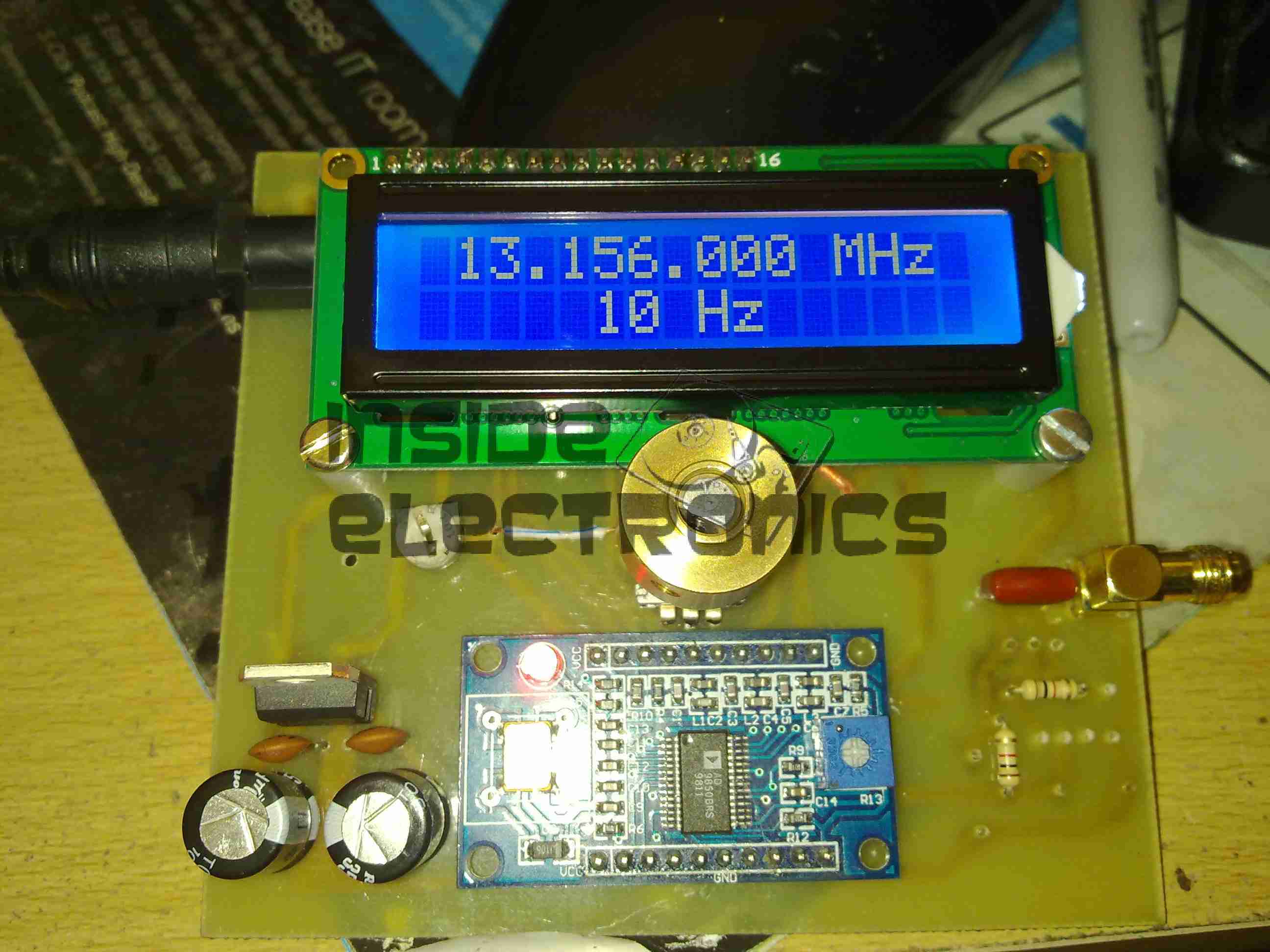
Continuing from my previous post where I published an Eagle design layout for AD7C‘s Arduino powered VFO, here is a completed board.
I have made some alterations to the design since posting, which are reflected in the artwork download in that post, mainly due to Eagle having a slight psychotic episode making me ground one of the display control signals!
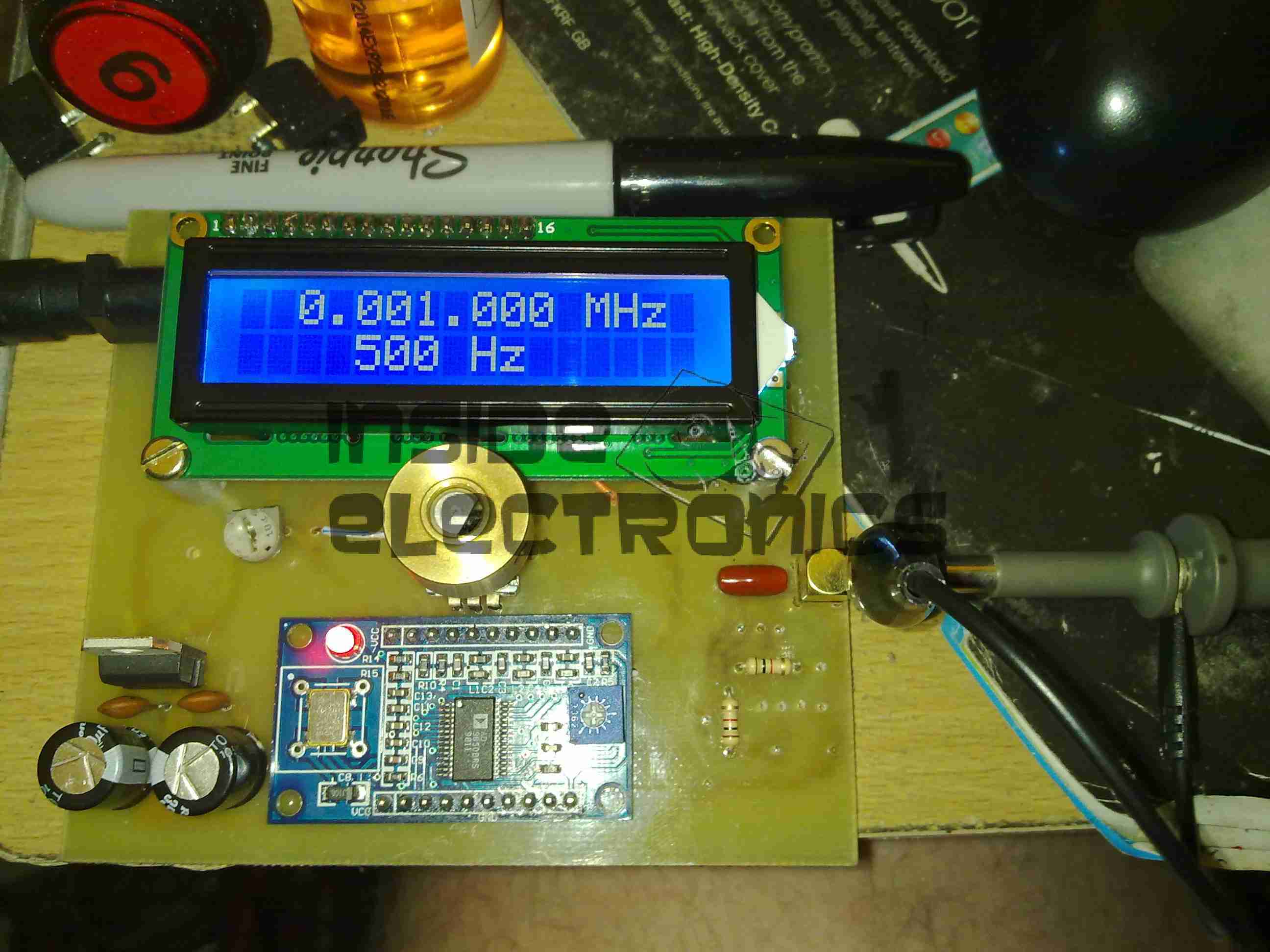
AD9850 VFO
The amplifier section is unpopulated & bypassed as I was getting some bad distortion effects from that section, some more work is needed there.
The Arduino Pro Mini is situated under the display, and the 5v rail is provided by the LM7805 on the lower left corner.
Current draw at 12v input is 150mA, for a power of 1.8W total. About 1W of this is dissipated in the LM7805 regulator, so I have also done a layout with an LM2574 Switching Regulator.
The SMPS version should draw a lot let power, as less is being dissipated in the power supply, but this version is more complex.
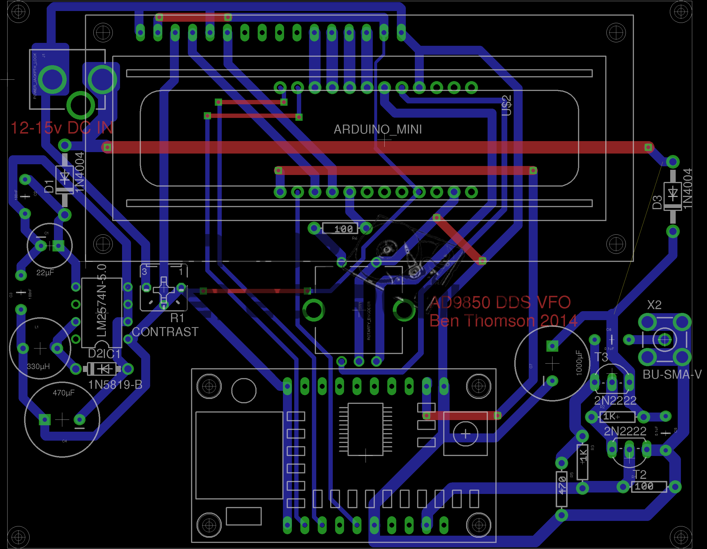
DDS VFO-SMPS
Here the SMPS circuit can be seen on the left hand side of the board, completely replacing the linear regulator.
I have not yet built this design, so I don’t know what kind of effect this will have on the output signal, versus the linear regulator. I have a feeling that the switching frequency of the LM2574 (52kHz) might produce some interference on the output of the DDS module. However I have designed this section to the standards in the datasheet, so this should be minimal.
Nevertheless this version is included in the Downloads section at the bottom of this post.
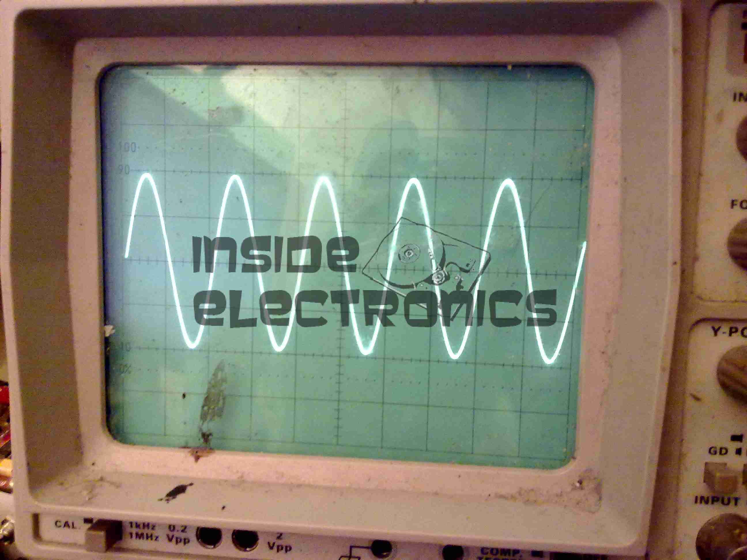
The output coupled through a 100nF capacitor is very clean, as can be seen below, outputting a 1kHz signal. Oscilloscope scale is 0.5ms/div & 1V/div.
VFO Output (Mucky ‘Scope)Scope Connected
Thanks again to Rich over at AD7C for the very useful tool design!
Linked below is the Eagle design files for this project, along with my libraries used to create it.
After 13 months of very heavy use at various events, festivals & boat trips, the Li-Po battery pack at the heart of my portable power supply has died.
What initially started as one cell inflating spread to the other cells in the pack over a period of about 3 months, so I have completely replaced the pack with a larger unit.
New Pack
The old pack was an 8.8Ah unit at 12.6v. By using smaller burst capacity cells, I have managed to squeeze in a total of 13.2Ah, still leaving space to spare for an extra 3 cell string along the top.
Cell Interconnects
Here is the end of the battery pack, with all the cell interconnects. There are 3 2.2Ah cells in series to give the 12.6v terminal voltage, with 6 of those strings in parallel to give the total Ah rating.
A new charging circuit will be implemented to better handle the volatile chemistry of Li-Po cells, hopefully this will result in the pack lasting longer than a year!
The new higher capacity will hopefully help with power requirements at future events, still being charged during the day by a 24W solar panel, but at night will have to cope with charging two smartphones, two eCigs & running a few watts of LED lighting.
The trial-by-fire will be this year’s Download Festival in June, when I will be operating off-grid for 6 days.
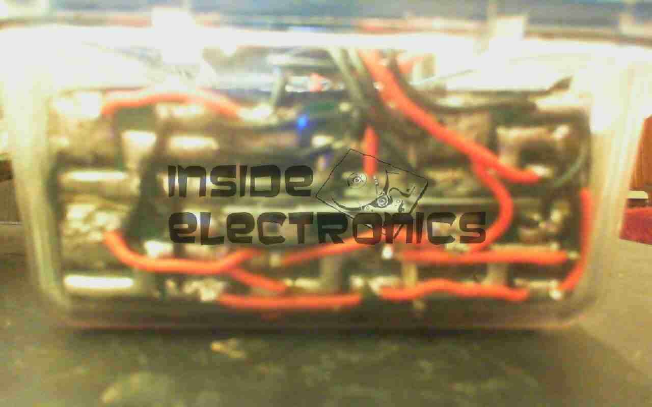
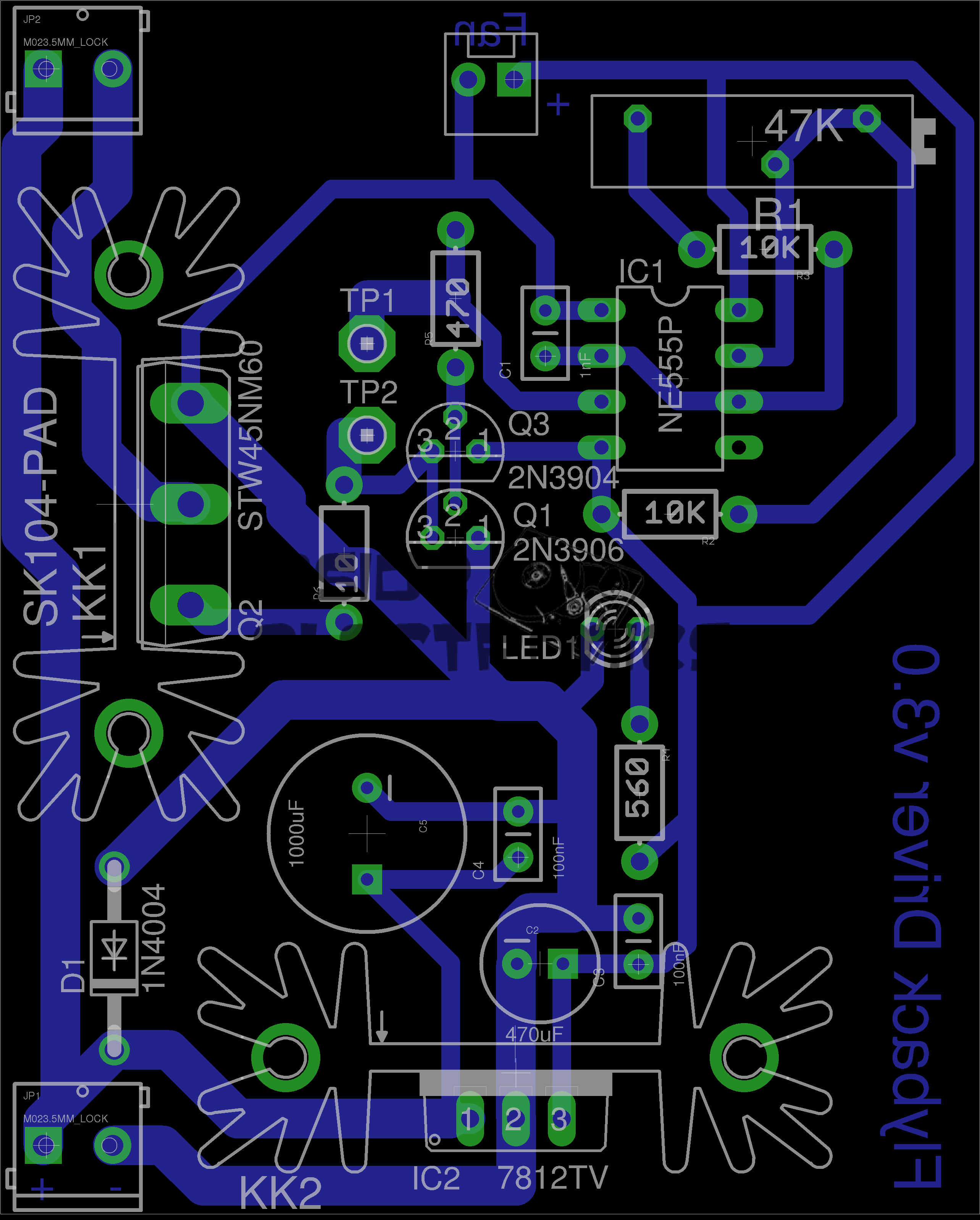
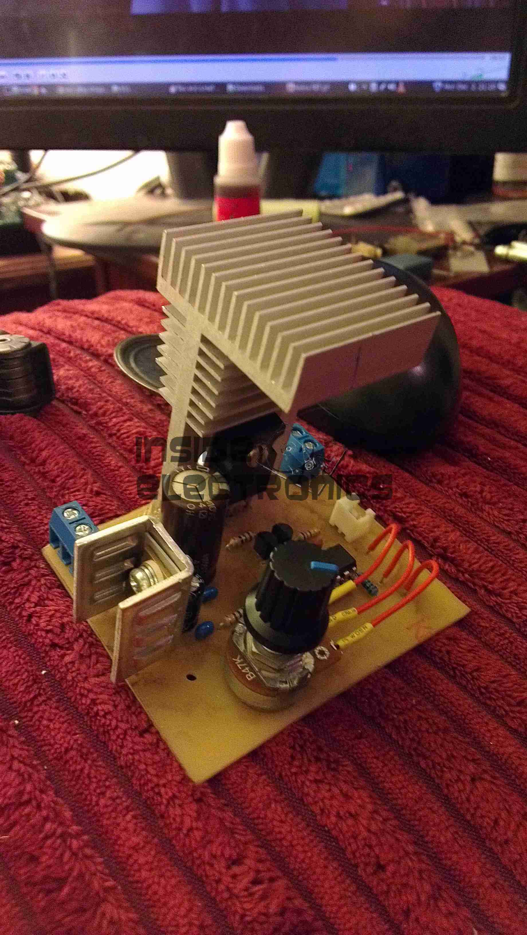
Here is a simple 555 timer based flyback transformer driver, with the PCB designed by myself for some HV experiments. Above is the Eagle CAD board layout.
The 555 timer is in astable mode, generating a frequency from about 22kHz to 55kHz, depending on the position of the potentiometer. The variable frequency is to allow the circuit to be tuned to the resonant frequency of the flyback transformer in use.
This is switched through a pair of buffer transistors into a large STW45NM60 MOSFET, rated at 650v 45A.
Input power is 15-30v DC, as the oscillator circuit is fed from an independent LM7812 linear supply.
Provision is also made on the PCB for attaching a 12v fan to cool the MOSFET & linear regulator.
Initial Board
Board initially built, with the heatsink on the linear regulator fitted. I used a panel mount potentiometer in this case as I had no multiturn 47K pots in stock.
PCB Traces
Bottom of the PCB. The main current carrying traces have been bulked up with copper wire to help carry the potentially high currents on the MOSFET while driving a large transformer.
This board was etched using the no-peel toner transfer method, using parchement paper as the transfer medium.
MOSFET Heatsinked
Main MOSFET now fitted with a surplus heatsink from an old switchmode power supply. A Fan could be fitted to the top of this sink to cope with higher power levels.
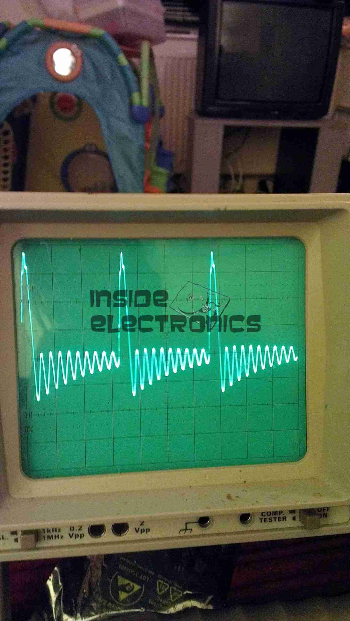
Gate Drive Waveform
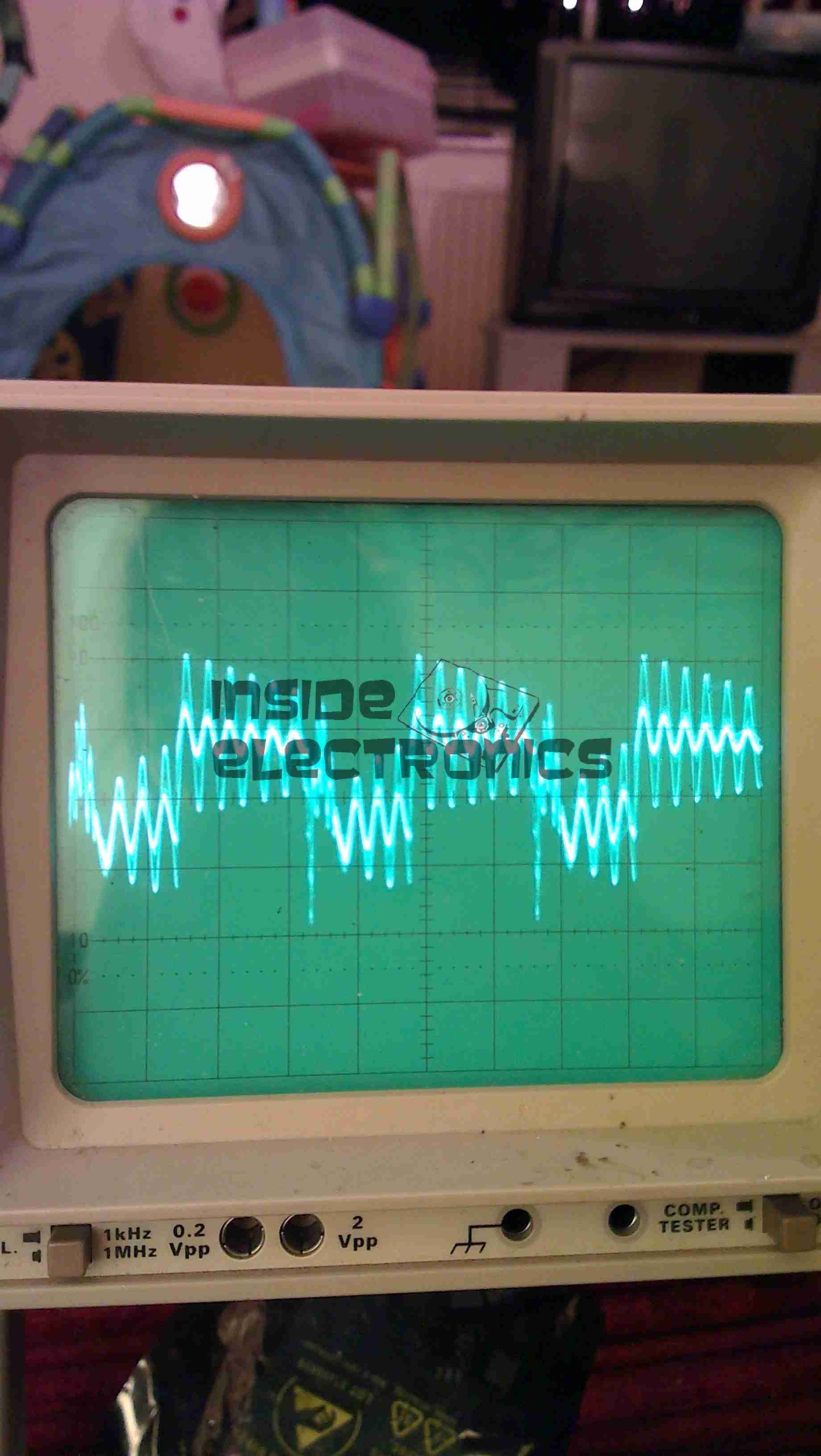
This is the gate drive waveform while a transformer is connected, the primary is causing some ringing on the oscillator. The waveform without an attached load is a much cleaner square wave.
Flyback Secondary Waveform
I obtained a waveform of the flyback secondary output by capacitively coupling the oscilloscope probe through the insulation of the HT wire. The pulses of HV can be seen with the decaying ringing of the transformer between cycles.
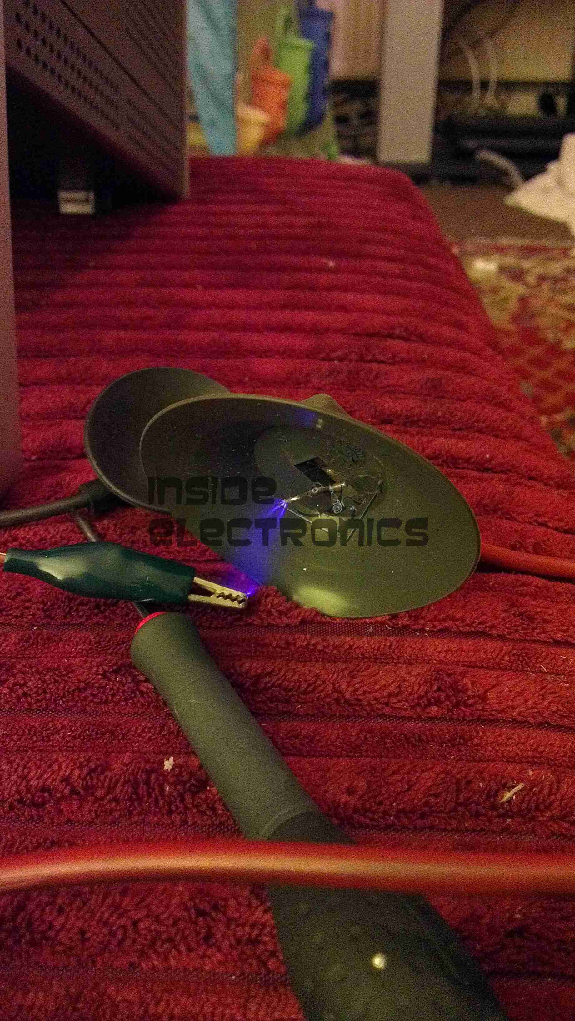
Corona DischargeArc Discharge
Corona & arc discharges at 12v input voltage.
Download the Eagle schematic files here: [download id=”5561″]
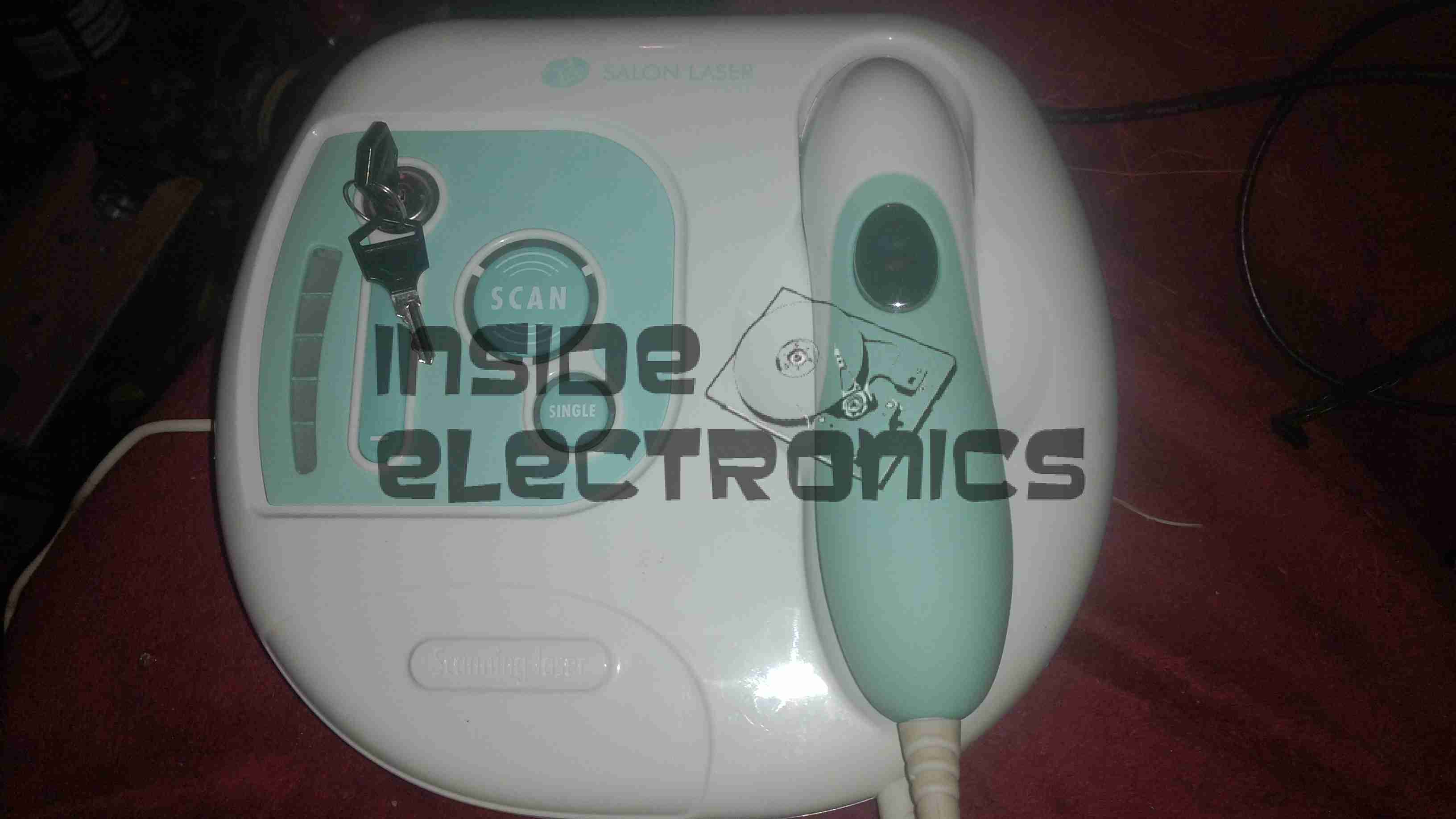
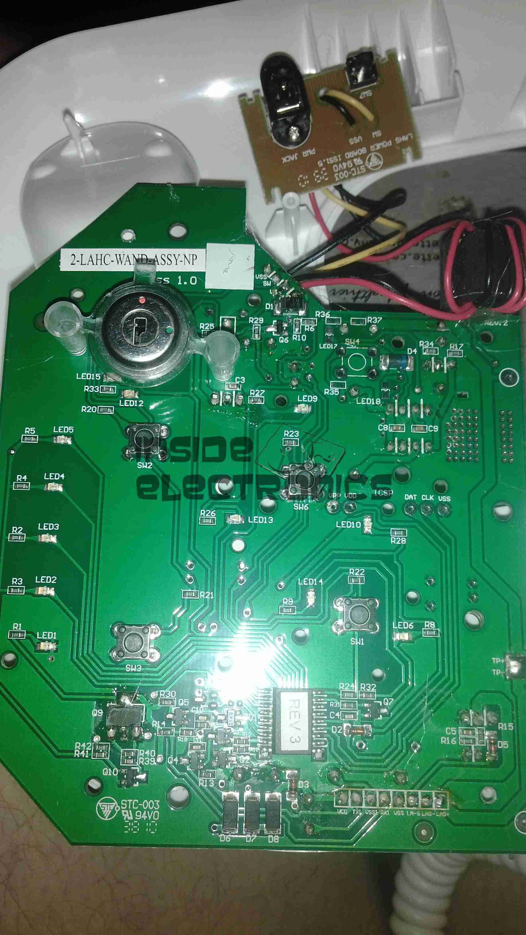
Here is a home laser hair removal unit, a Rio LAHS4. Shown above is the system overview, with the laser wand & the user controls.
Main PCB Top
Main base unit popped open reveals the main PCB, with the central processor, a PIC16F628A.
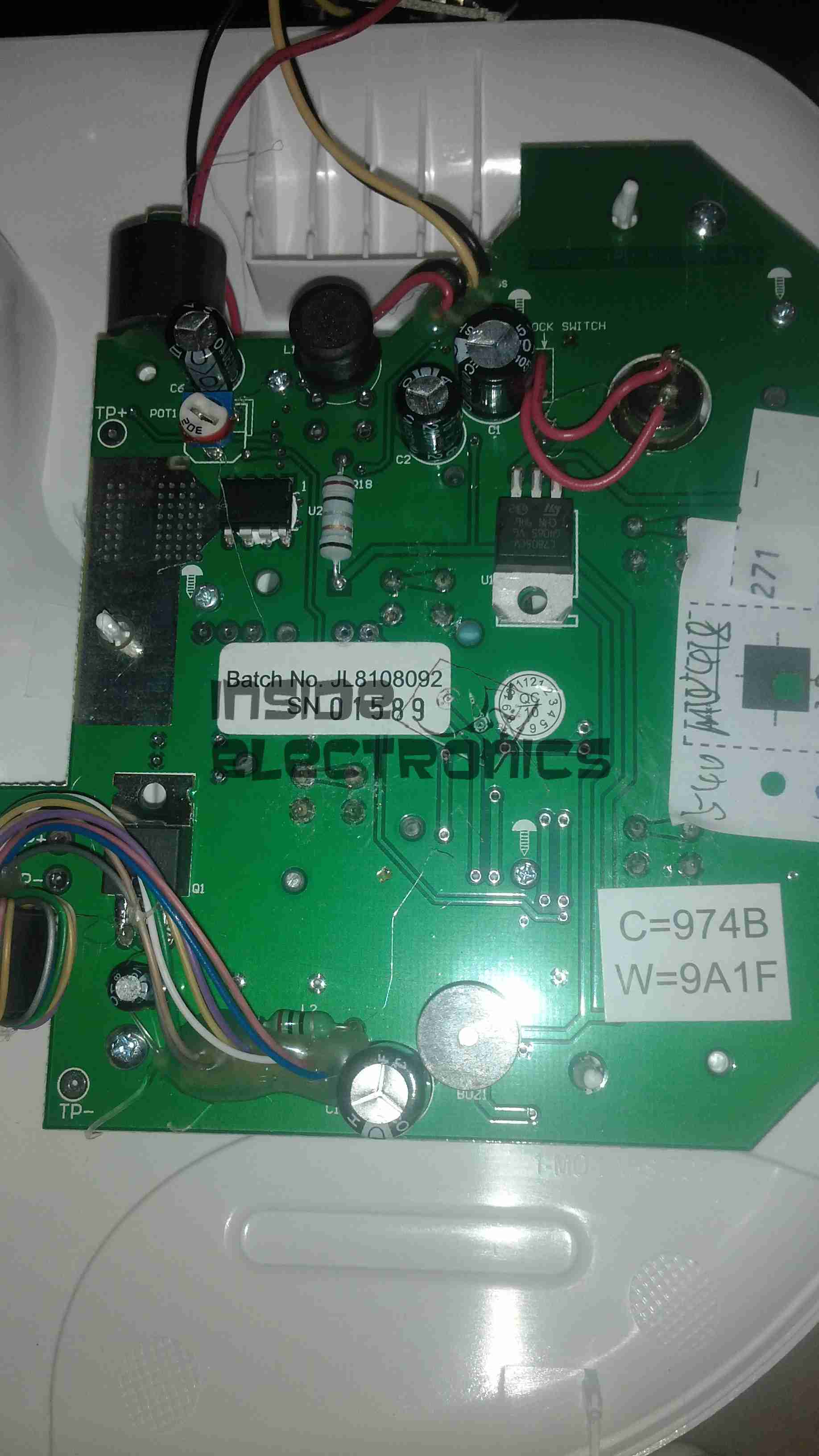
Main PCB Bottom
Other side of the PCB is mainly populated with power supply & filtering for the logic sections.
Wand PCB
Cracking open the laser wand reveals a stacked pair of PCBs, a main laser controller & the capacitive sensor PCB. This capacitive sensor connects to a pair of pins on the laser head & prevents operation if the unit is not held firmly against the skin.
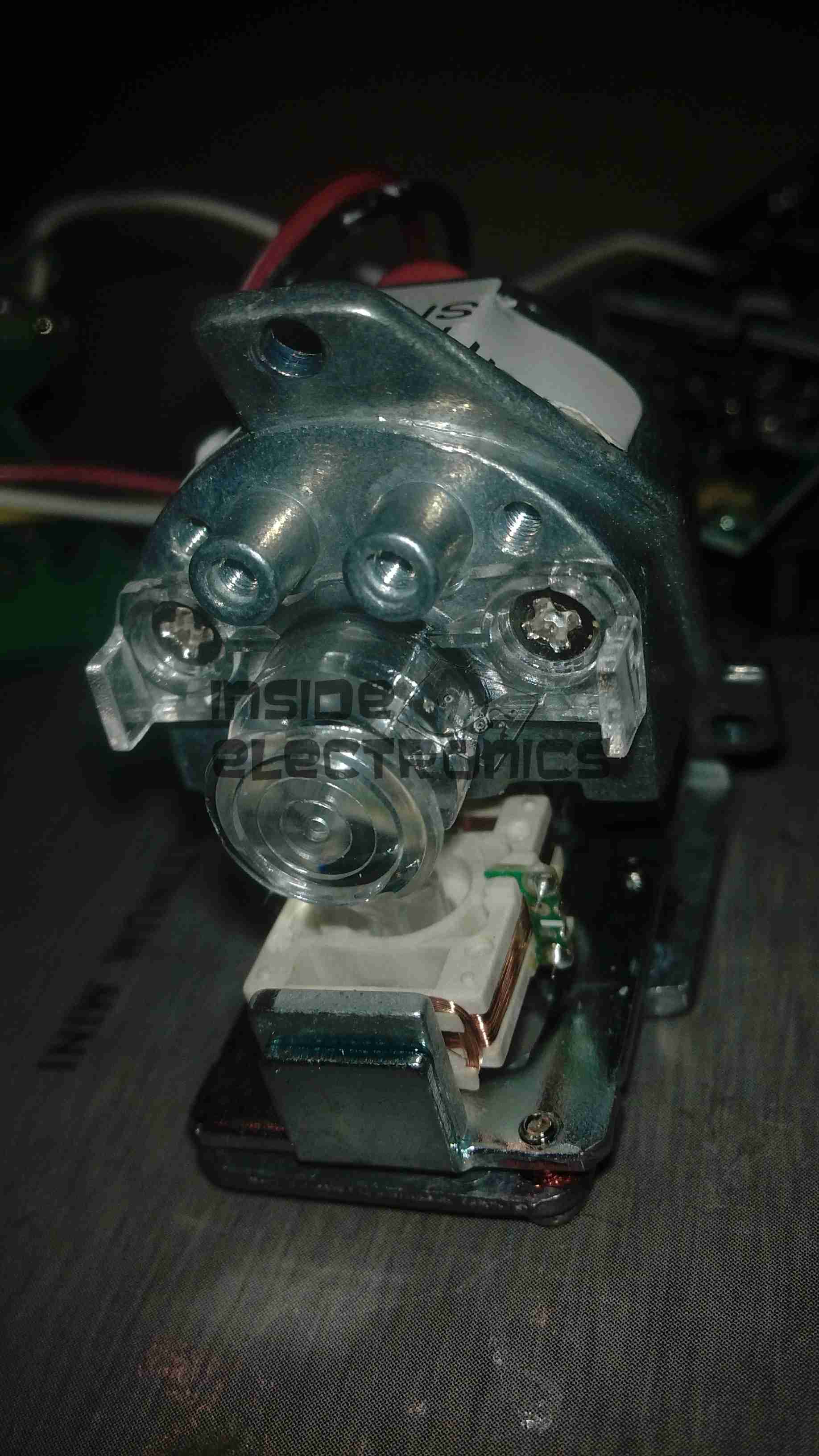
Diode Module
Front of the laser diode module with the movable lens, on a pair of voice coil actuators. Very similar to the lens positioner used in any CD/DVD player pickup assembly.
The diode in this unit is an 808nm chip, with power in the 300-600mW range most likely.
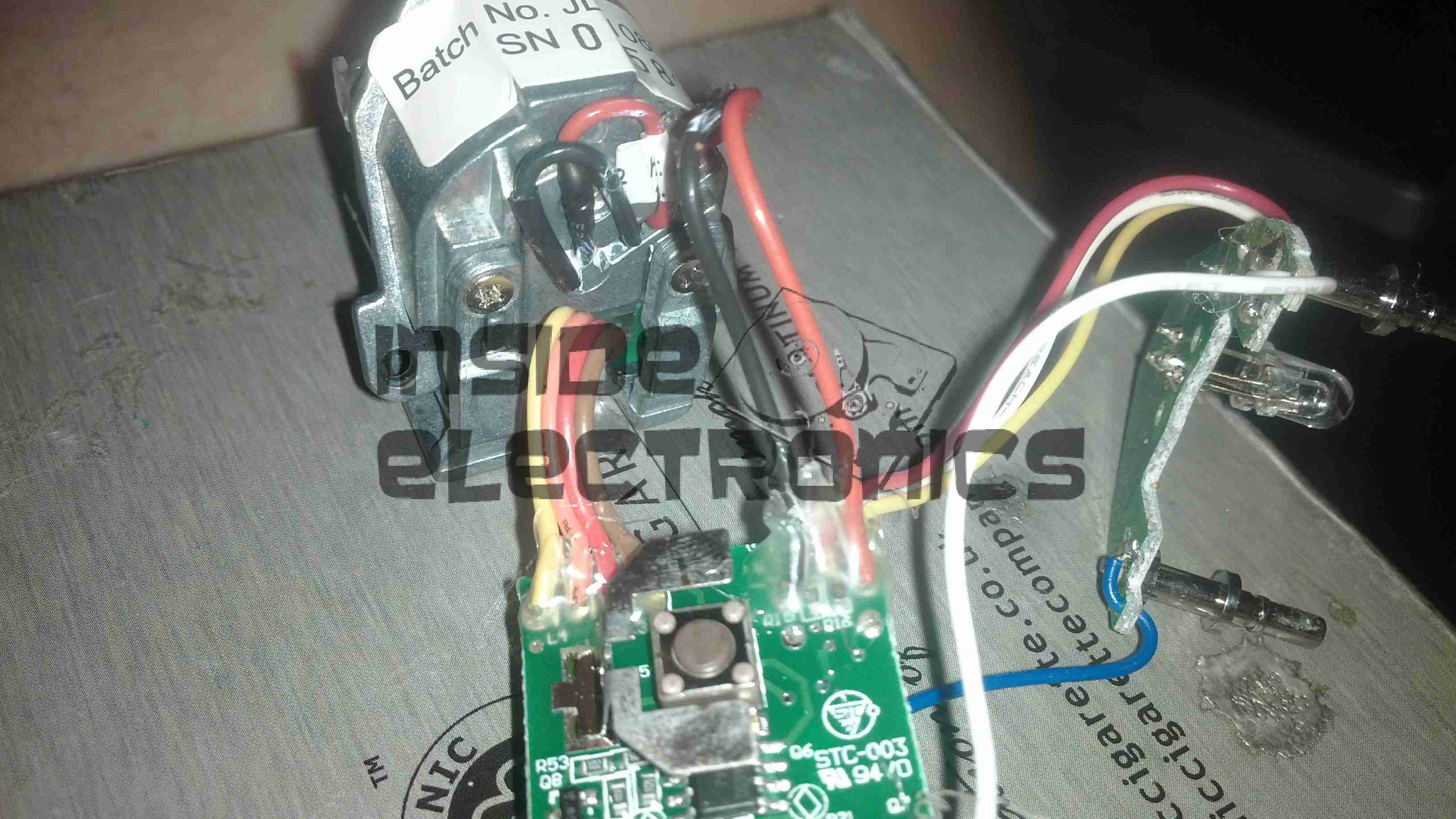
Diode Module Rear
Rear of the diode module, with the connections to the diode itself & the voice coil positioner for the lens.
Wand PCB Top
Other side of the wand PCB, showing the capacitive sensor board on top of the main controller board. There is another CPU on the board here, which most likely communicates with the main processor in the base through a serial connection.
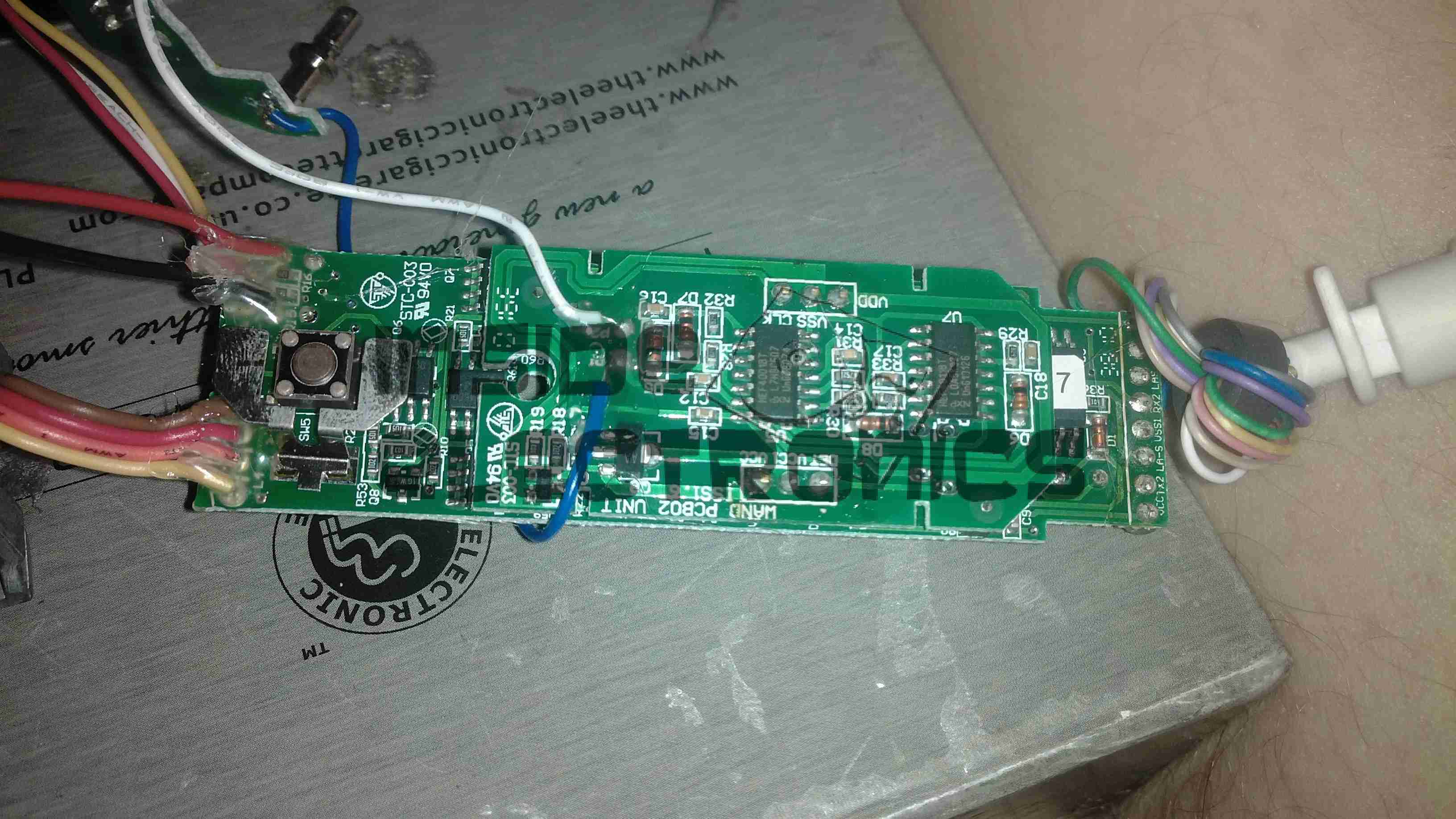
Here is an AVR powered optical tachometer design, that I adapted from the schematic found here.
I made a couple of changes to the circuit & designed a PCB & power supply module to be built in. The original design specified a surface mount IR LED/Photodiode pair, however my adjustment includes a larger IR reflectance sensor built onto the edge of the board, along with a Molex connector & a switch to select an externally mounted sensor instead of the onboard one.
There is also an onboard LM7805 based power supply, designed with a PCB mount PP3 battery box.
The power supply can also be protected by a 350mA polyfuse if desired. If this part isn’t fitted, then a pair of solder bridge pads are provided within the footprint for the fuse to short out the pads.
For more information on the basic design, please see the original post with the link at the top of the page.
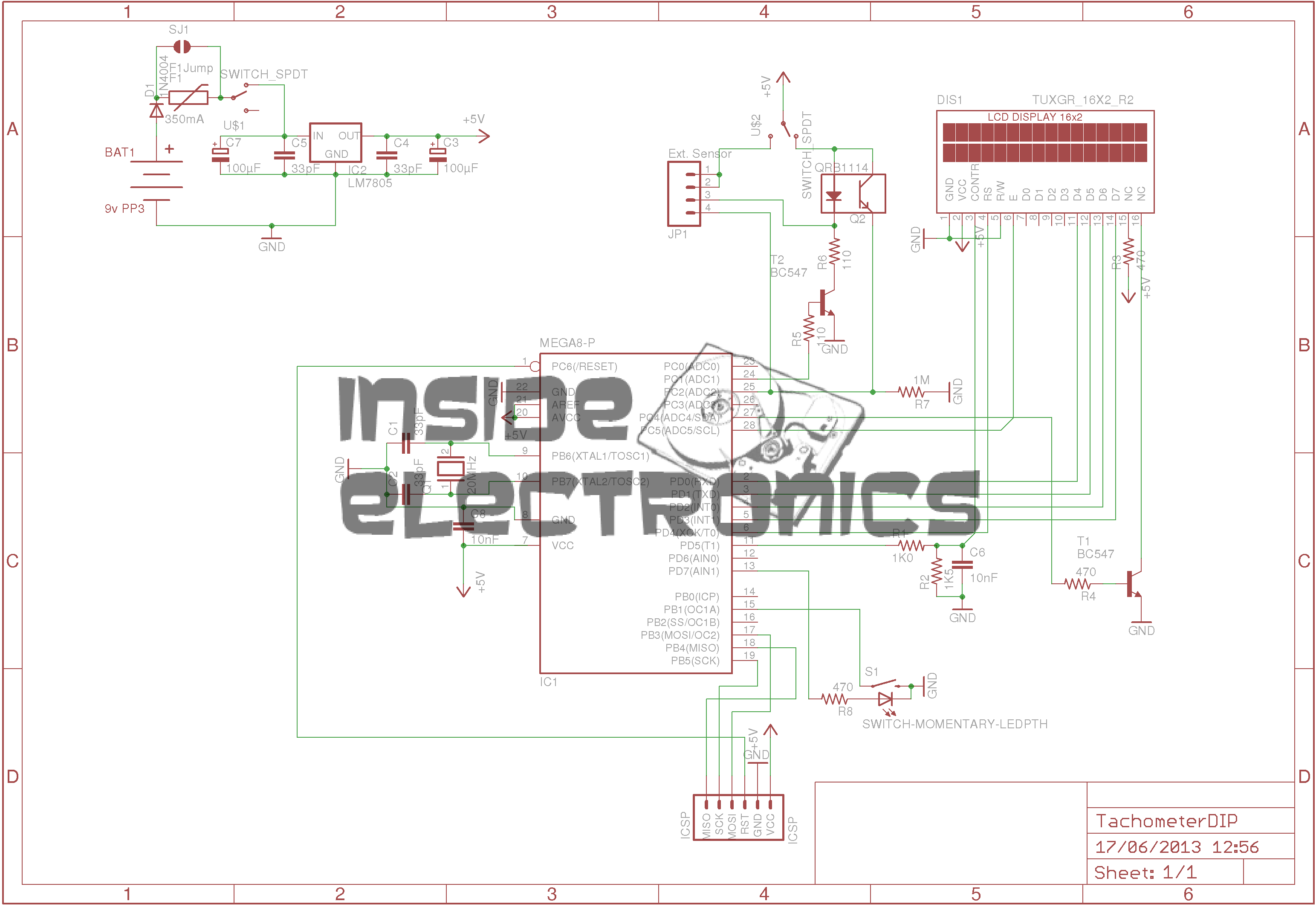
Schematic
Here is an archive of the firmware & the Eagle CAD files for the PCB & schematic design.
As the first USB hub I was using was certainly not stable – it would not enumerate between boots & to get it working again would require waiting around 12 hours before applying power, it has been replaced. This is a cheapie eBay USB hub, of the type shown below.
These hubs are fantastic for hobbyists, as the connections for power & data are broken out on the internal PCB into a very convenient row of pads, perfect for integration into many projects.
Breakout Hub
I now have two internal spare USB ports, for the inbuilt keyboard/mouse receiver & the GPS receiver I plan to integrate into the build.
These hubs are also made in 7-port versions, however I am not sure if these have the same kind of breakout board internally. As they have the same cable layout, I would assume so.
Connector Panel
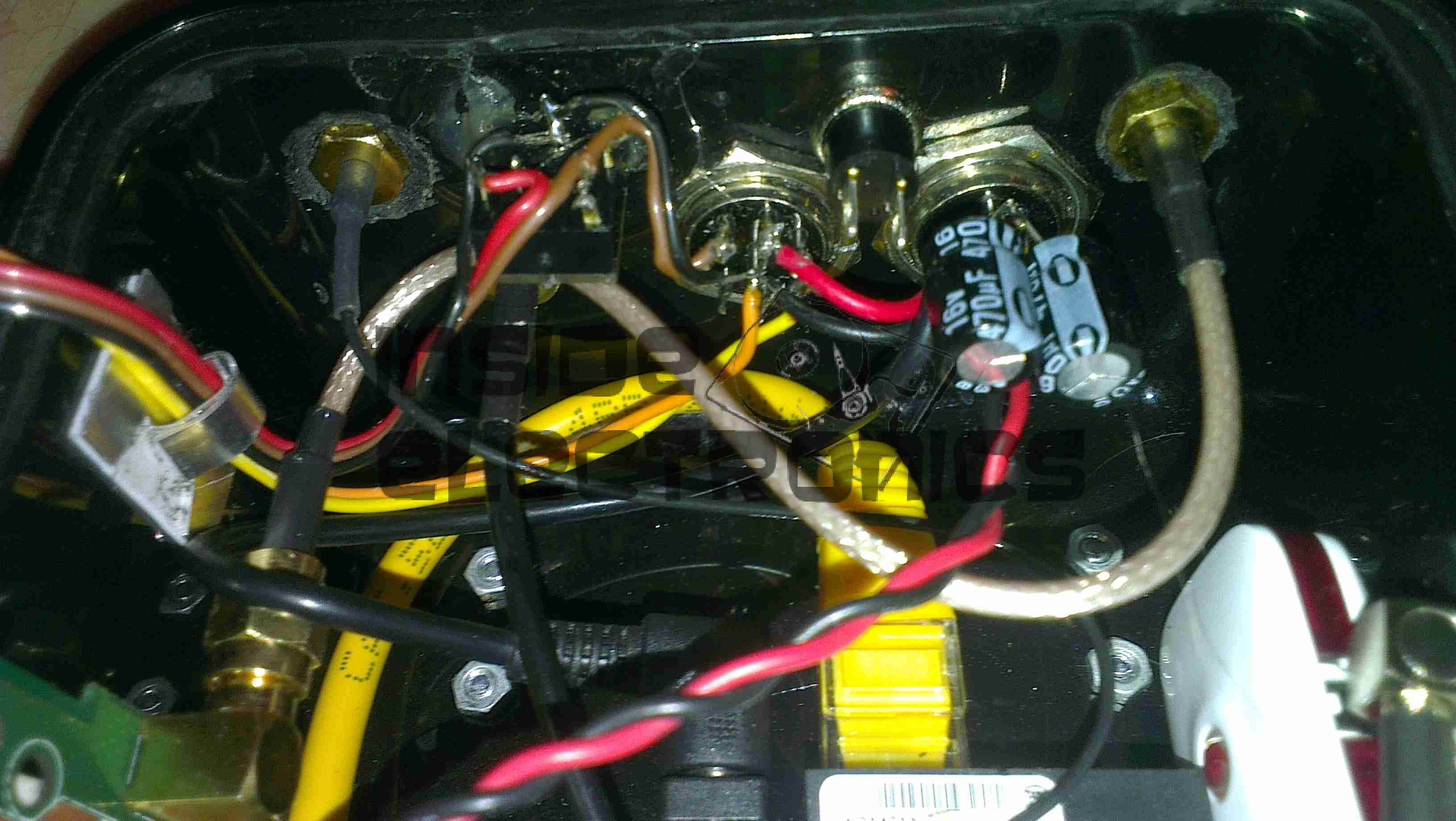
Here is a closeup of the back of the connectors, showing a couple of additions.
I have added a pair of 470µF capacitors across the power rails, to further smooth out the ripple in the switching power supply, as I was having noise issues on the display.
Also, there is a new reset button added between the main interface connectors, which will be wired into the pair of pads that the Raspberry Pi has to reset the CPU.
This can be used as a power switch in the event the Pi is powered down when not in use & also to reset the unit if it becomes unresponsive.
Tip Jar
If you’ve found my content useful, please consider leaving a donation by clicking the Tip Jar below!
All collected funds go towards new content & the costs of keeping the server online.