Posted on 3 Comments

Arduino Based SWR/PWR Meter – The Board

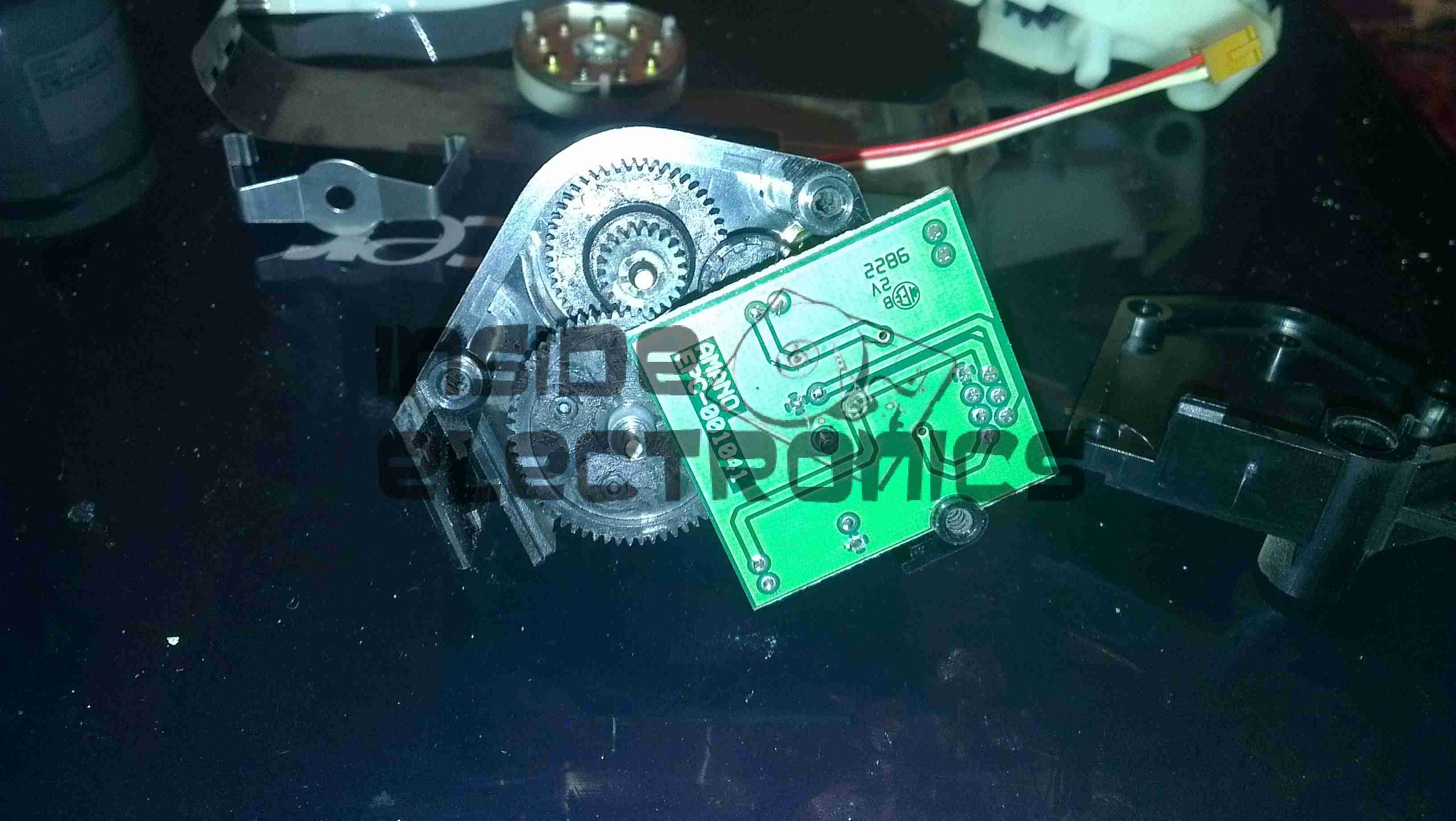
I recently posted about a small analog SWR/Power meter I got from eBay, and figured it needed some improvement.

After some web searching I located a project by ON7EQ, an Arduino sketch to read SWR & RF power from any SWR bridge.
The Arduino code is on the original author’s page above, his copyright restrictions forbid me to reproduce it here.

I have also noticed a small glitch in the code when it is flashed to a blank arduino: The display will show scrambled characters as if it has crashed. However pushing the buttons a few times & rebooting the Arduino seems to fix this. I think it’s related to the EEPROM being blank on a new Arduino board.

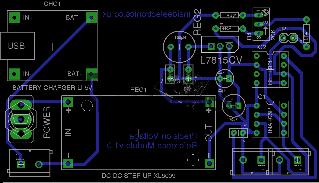
I have run a board up in Eagle for testing, shown below is the layout:

SWR Meter SCH
SWR Meter SCH

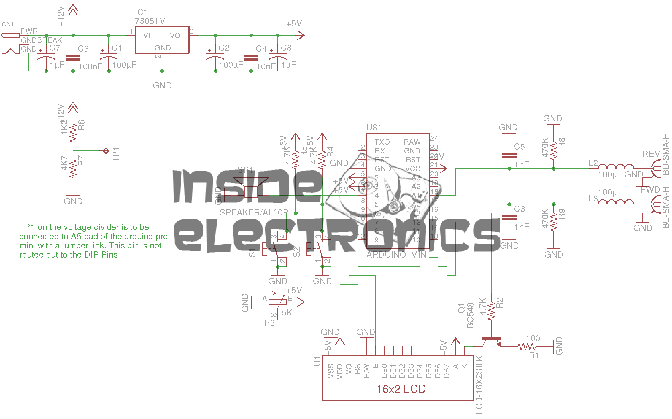
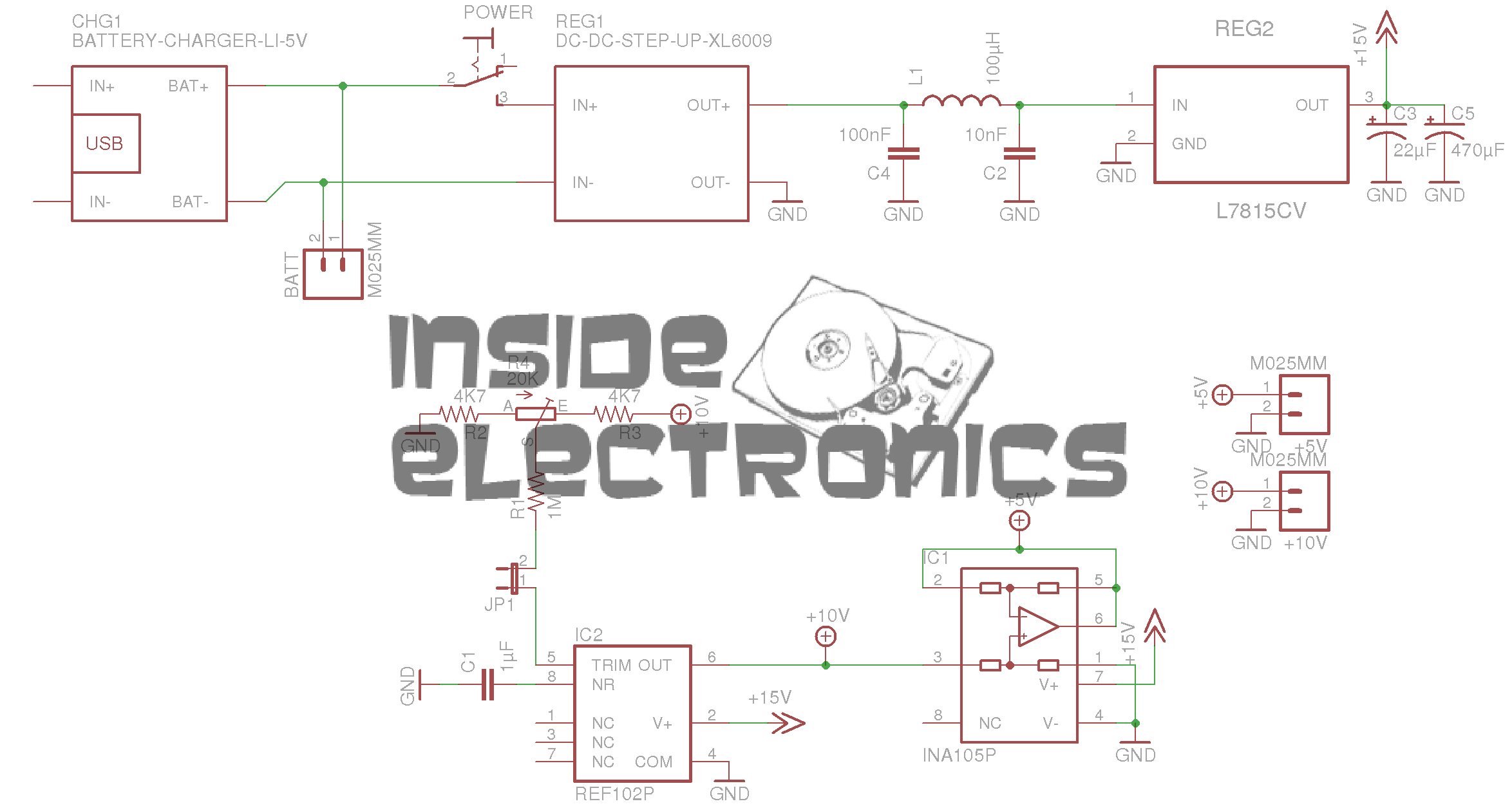
The Schematic is the same as is given on ON7EQ’s site.
Update: ON7EQ has kindly let me know I’ve mixed up R6 & R7, so make sure they’re switched round when the board is built ;). Fitting the resistors the wrong way around may damage the µC with overvoltage.

SWR Meter PCB
SWR Meter PCB

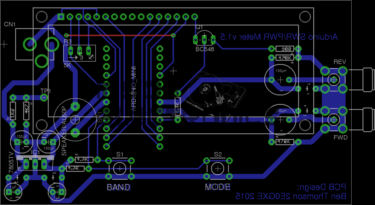
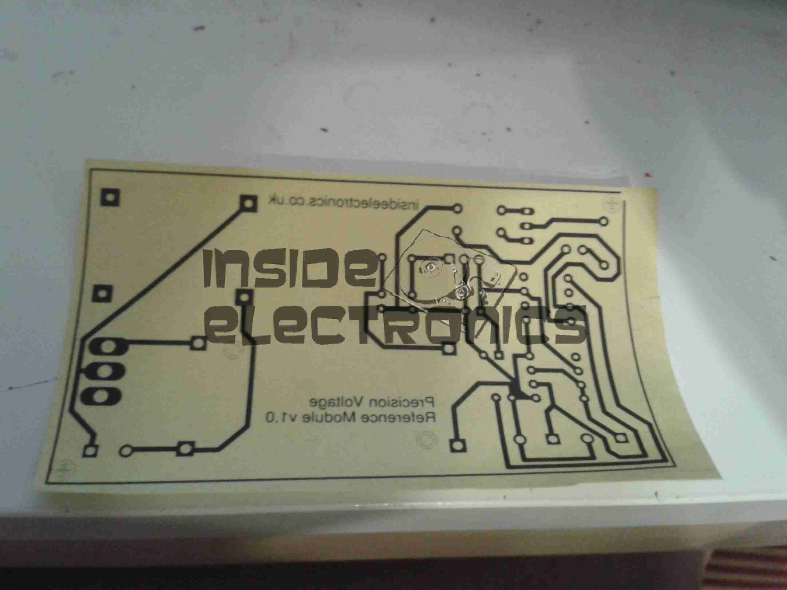
Here’s the PCB layout. I’ve kept it as simple as possible with only a single link on the top side of the board.

PCB Top
PCB Top

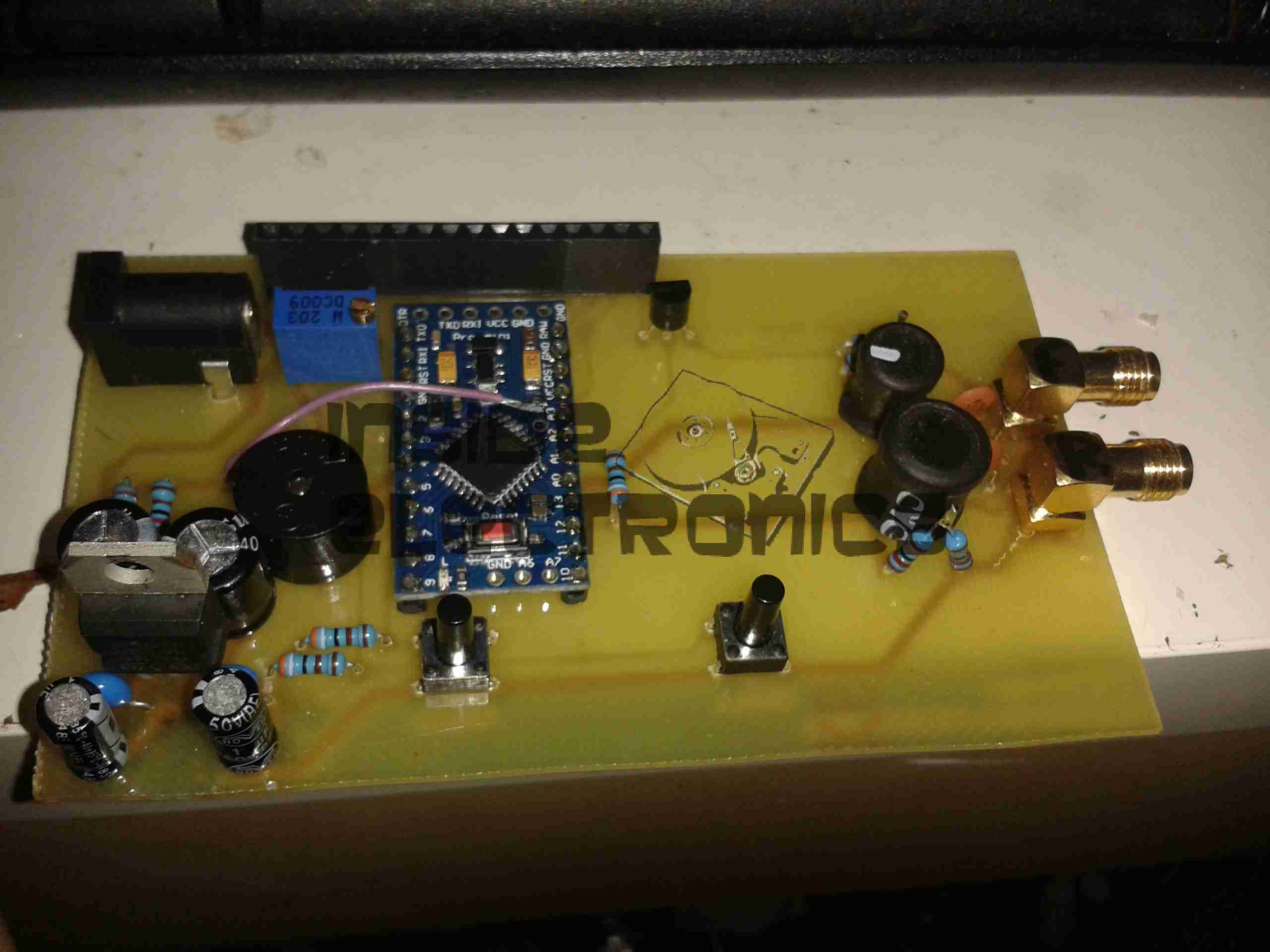
Here’s the freshly completed PCB ready to rock. Arduino Pro mini sits in the center doing all the work.
The link over to A5 on the arduino can be seen here, this allows the code to detect the supply voltage, useful for battery operation.
On the right hand edge of the PCB are the pair of SMA connectors to interface with the SWR bridge. Some RF filtering is provided on the inputs.

PCB Bottom
PCB Bottom

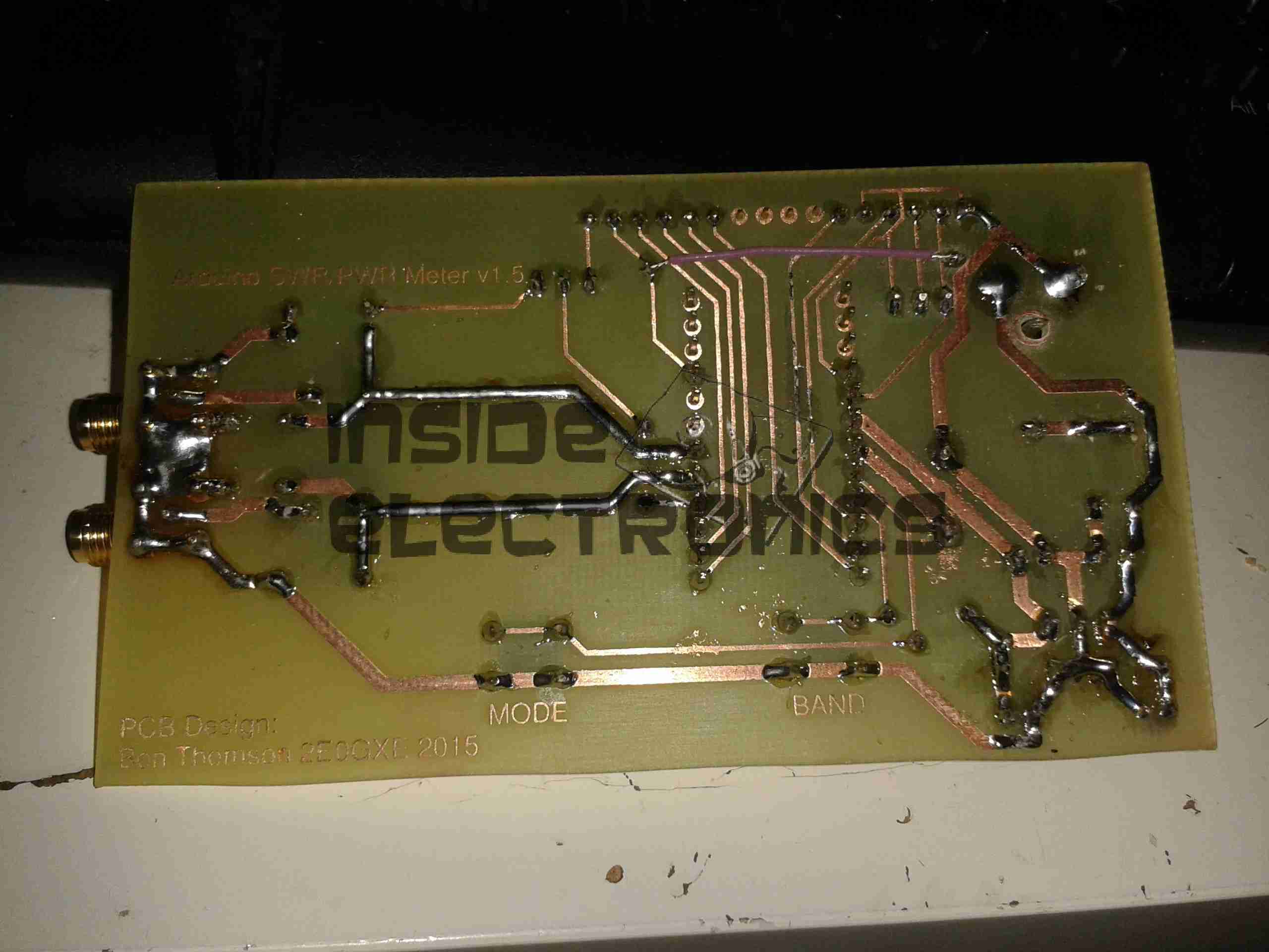
Trackside view of the PCB. This was etched using my tweaked toner transfer method.

LCD Fitted
LCD Fitted

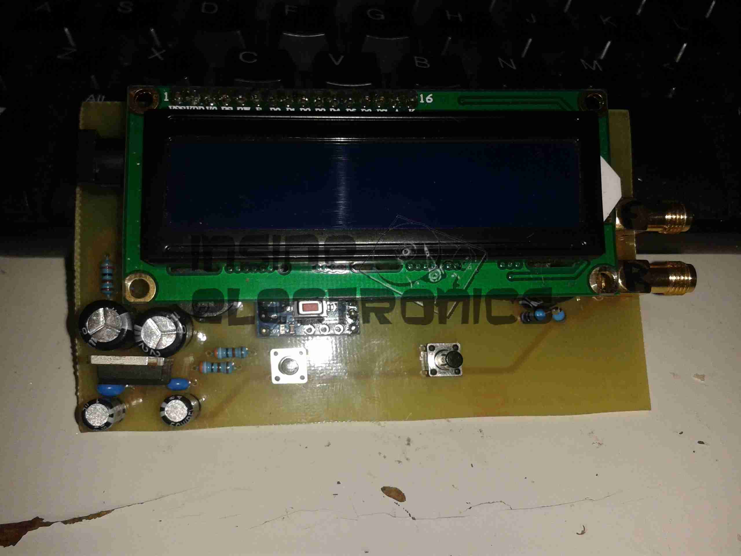
Here the board has it’s 16×2 LCD module.

Online
Online

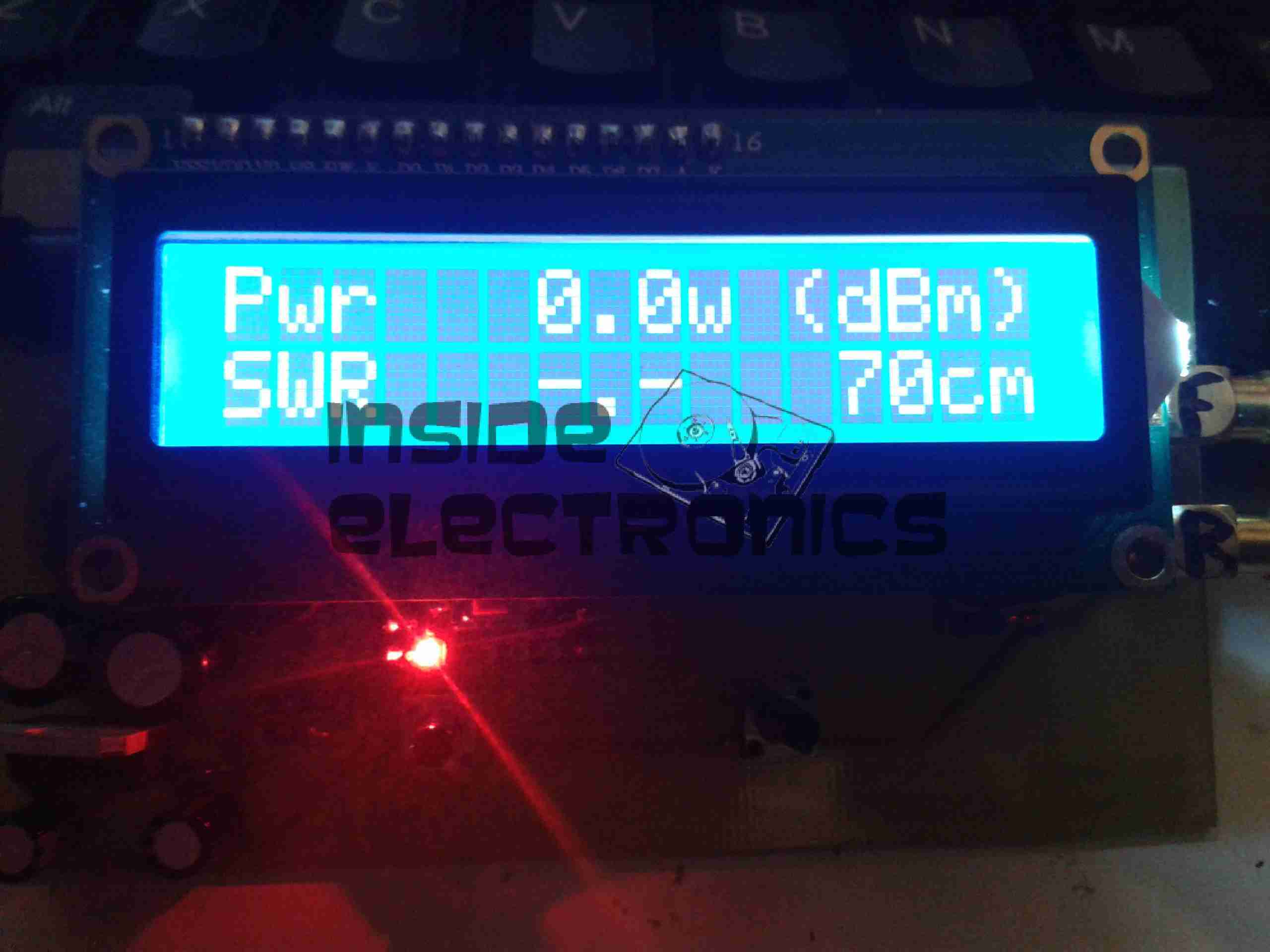
Board powered & working. Here it’s set to the 70cm band. The pair of buttons on the bottom edge of the board change bands & operating modes.
As usual, the Eagle layout files are available below, along with the libraries I use.

[download id=”5585″]

[download id=”5573″]

More to come on this when some components arrive to interface this board with the SWR bridge in the eBay meter.

Posted on Leave a comment

Precision 10v & 5v Reference

After watching a video over at Scullcom Hobby Electronics on YouTube, I figured I’d build one of these precision references to calibrate my multimeters.

It’s based around a REF102P 10v precision reference & an INA105P precision unity gain differential amplifier.

For full information, check out the video, I won’t go into the details here, just my particular circuit & PCB layout.

In the video, Veroboard is used. I’m not too fond of the stuff personally. I find it far too easy to make mistakes & it never quite looks good enough. To this end I have spun a board in Eagle, as usual.

Precision Ref SCH
Precision Ref SCH – Click to Embiggen

Here’s the schematic layout, the same as is in the video.

Precision Ref BRD
Precision Ref BRD

As usual, the Eagle CAD layout files can be found at the bottom of the post.

And the associated PCB layout. I have added the option to be able to tweak the output, to get a more accurate calibration, which can be added by connecting JP1 on the PCB.

As in the original build, this unit uses pre-built DC-DC converter & Li-Ion charger modules. A handy Eagle library can be found online for these parts.
I have however left off the battery monitor section of the circuit, since I plan to use a protected lithium cell for power. This also allowed me to keep the board size down, & use a single sided layout.

Toner Transfer Paper

Here’s the track layout ready to iron onto the copper clad board. I use the popular toner transfer system with special paper from eBay, this stuff has a coating that allows the toner to easily be transferred to the PCB without having to mess about with soaking in water & scraping paper off.

Ironed On
Ironed On

Here’s the paper having just been ironed onto the copper. After waiting for the board to cool off the paper is peeled off, leaving just the toner on the PCB.

Etched PCB
Etched PCB

PCB just out of the etch tank, drilled & with the solder pins for the modules installed. Only one issue with the transfer, in the bottom left corner of the board is visible, a very small section of copper was over etched.
This is easily fixed with a small piece of wire.

Components Populated

Main components populated. The DC-DC converter is set at 24v output, which the linear regulator then drops down to the +15v rail for the reference IC. The linear section of the regulator, along with the LC filter on the output of the switching regulator produce a low-ripple supply.

SMPS Ripple
SMPS Ripple

Here’s the scope reading the AC ripple on the output of the DC-DC converter. Scale is 100mV/Div. Roughly 150mV of ripple is riding on top of the DC rail.

Linear PSU Ripple
Linear PSU Ripple

And here’s the output from the linear regulator, scale of 50mV/Div. Ripple has been reduced to ~15mV for the reference IC.
In total the circuit as built has a power consumption of ~0.5W, most of which is being dissipated as heat in the linear part of the PSU.

[download id=”5583″]

Posted on Leave a comment

HPI Savage X 4.6 LiPo Receiver Battery

3S Lithium-Polymer Pack

To provide more run time with the conversion to petrol & spark ignition, I have also upgraded the on-board electronics supply to compensate for the extra ~650mA draw of the ignition module.
This modification is centred around a 3S Lithium-Polymer battery pack, providing a nominal 11.1v to a voltage regulator, which steps down this higher voltage to the ~6v required by the receiver & servo electronics.

Power Regulator
Power Regulator
Power Regulator
Power Regulator

The regulator, shown above, is a Texas Instruments PTN78060WAZ wide-input voltage adjustable regulator. This module has an exceptionally high efficiency of ~96% at it’s full output current of 3A. The output voltage is set by a precision resistor, soldered to the back of the module, in this case 6.5v. Standard RC connectors are used on the regulator to allow connection between the power switch & the radio receiver.

Receiver Box
Receiver Box

Everything tucked away into place inside the receiver box. The 3S 1000mAh LiPo fits perfectly in the space where the original Ni-Mh hump pack was located.
The completely stable output voltage of the regulator over the discharge curve of the new battery gives a much more stable supply to the radio & ignition, so I should experience fewer dropouts. Plus the fact that the engine now relies on power from the receiver pack to run, it’s a built in fail safe – if the power dies to the receiver, the engine also cuts out.

Posted on Leave a comment

Wearable Raspberry Pi Part 2.5 – Battery Pack PCM

Battery PCM
Battery PCM

The final part for the battery pack has finally arrived, the PCM boards. These modules protect the cells by cutting off the power at overcharge, undercharge & overcurrent. Each cell is connected individually on the right, 12v power appears on the left connections. These modules also ensure that all the cells in the pack are balanced.


Posted on Leave a comment

Wearable Raspberry Pi Part 2 – Power Supply

All Fitted
All Fitted

Progress is finally starting on the power supply unit for the Pi, fitted into the same case style as the Pi itself, this is an 8Ah Li-Poly battery pack with built in voltage regulation.

Regulator Boards
Regulator Boards

Here are the regulators, fixed to the top of the enclosure. These provide the 12v & 5v power rails for the Pi unit, at a max 3A per rail.

Battery Pack
Battery Pack

In the main body of the case the battery pack is fitted. This is made up of 4 3-cell Li-Poly RC battery packs, rated at 2Ah each. All wired in parallel this will provide a total of 8Ah at 12.6v when fully charged.

Powered Up
Powered Up

Here the regulators are powered up from a 13v supply for testing. I have discovered at full load these modules have very bad ripple, so I will be adding extra smoothing capacitors to the power rails to compensate for this.

I/O
I/O

Here are the connectors on the top of the unit, outputting the two power rails to the Pi & the DC barrel jack that will be used to charge the pack.


Posted on Leave a comment

Amano PIX 3000x Timeclock

Front
Front

This is a late 90’s business timeclock, used for maintaining records of staff working times, by printing the time when used on a sheet of card.

Front Internal
Front Internal

Here is the top cover removed, which is normally locked in place to stop tampering. The unit is programmed with the 3 buttons & the row of DIP switches along the top edge.

Instructions
Instructions

Closeup of the settings panel, with all the various DIP switch options.

CPU & Display
CPU & Display

Cover plate removed from the top, showing the LCD & CPU board, the backup battery normally fits behind this. The CPU is a 4-bit microcontroller from NEC, with built in LCD driver.

PSU & Drivers
PSU & Drivers

Power Supply & prinhead drivers. This board is fitted with several NPN Darlington transistor arrays for driving the dox matrix printhead.

Printhead
Printhead

Printhead assembly itself. The print ribbon fits over the top of the head & over the pins at the bottom. The drive hammers & solenoids are housed in the circular top of the unit.

Printhead Bottom
Printhead Bottom

Bottom of the print head showing the row of impact pins used to create the printout.

2013-02-13 18.00.09Bottom of the solenoid assembly with the ribbon cable for power. There are 9 solenoids, to operate the 9 pins in the head.

Return Spring
Return Spring

Top layer of the printhead assembly, showing the leaf spring used to hold the hammers in the correct positions.

Hammers
Hammers

Hammer assembly. The fingers on the ends of the arms push on the pins to strike through the ribbon onto the card.

Solenoids
Solenoids

The ring of solenoids at the centre of the assembly. These are driven with 3A darlington power arrays on the PSU board.

Gearbox Internals
Gearbox Internals

There is only a single drive motor in the entire unit, that both clamps the card for printing & moves the printhead laterally across the card. Through a rack & pinion this also advances the ribbon with each print.


Posted on 1 Comment

MicroVision ShowWX+ HDMI Laser Pico Projector

Info
Info

Here’s the teardown of the projector itself! On the right is the info label from the projector, which covers the flex ribbon to the VGA/composite input board below.

This unit is held together with Allen screws, but is easy to get apart.


PicoP Display Engine

Here’s the insides of the projector, with just the top cover removed. The main board can be seen under the shielding can, the Micro HDMI connector is on the left & the MicroUSB connection is on the right. The USB connection is solely for charging the battery & provides no data interface to the unit.

On top of the main board is the shield can covering the PicoP Display Engine driver board, this shield was soldered on so no peek inside unfortunately!

Laser Module
Laser Module

The laser module itself is in the front of the unit, the laser assemblies are closest to the camera, on the left is the Direct Doubled Green module, in the centre is the blue diode, and the red diode on the right. Inside the module itself is an arrangement of mirrors & beamsplitters, used to combine the RGB beams from the lasers into a single beam to create any colour in the spectrum.

Module Innards
Module Innards


Here is the module innards revealed, the laser mounts are at the top of the screen, the green module is still mounted on the base casting.
The three dichroic mirrors in the frame do the beam combining, which is then bounced onto the mirror on the far left of the frame, down below the MEMs. From there a final mirror directs the light onto the MEMs scanning mirror before it leaves through the output window.

A trio of photodiodes caters for beam brightness control & colour control, these are located behind the last dichroic turning mirror in the centre of the picture.

Green Module Cavity
Green Module Cavity

This is inside the green laser module, showing the complexity of the device. This laser module is about the size of a UK 5p coin!

Green Module Labeled


And here on the left is the module components labelled.


Main PCB Top
Main PCB Top

Here is the main PCB, with the unit’s main ARM CPU on the right, manufactured by ST.

User buttons are along the sides.


Main PCB Bottom
Main PCB Bottom

Other side of the main board, with ICs that handle video input from the HDMI connector, battery charging via the USB port & various other management.


Posted on Leave a comment

Tornado eCig Battery Repair

This is just a few notes on the repair of an eCig battery (1Ah Tornado).

These batteries seem to have a flaw in which they will randomly stop working, while still displaying all the normal activity of the battery.
Here is what I have found.

Control PCB
Control PCB

Here the battery has been partially disassembled, with the control circuitry exposed here at the end of the unit. All the wiring here is fine & the electronics themselves are also OK, due to the LEDs still operating as normal when the button is pushed. The 1000mAh Li-Poly cell is to the right.

Ground Wire
Ground Wire

Here the end cap has been removed from the opposite end of the battery & the problem is found: the short wire here is the GND return for the atomiser, normally connected to the negative terminal of the battery in the tube, however here it has broken off.
This is most likely due to either the cell moving inside the tube during normal operation, weakening the solder joint, or simply a bad solder job from the factory. (This lead-free ROHS bullshit is to blame).

Repaired
Repaired

Here the wire has been successfully soldered back on to the battery tab. I have also added a small dab of hot glue to hold the battery in place on the inside of the tube, & replaced the solder on the joints with real 60/40 leaded solder. £15 saved.


Posted on Leave a comment

LED Lighting Part 1

Here I will document progress in replacing standard halogen MR10 lights with LEDs.

3x1W LED
3x1W LED

These units are from TruOpto, available through Rapid Electronics in the UK. They are 3W total, from 3x 1W emitters on an aluminium back plate.

LED Test Rig
LED Test Rig

Here is the LED attached to a heatsink for testing purposes – these units dissipate nearly 2W in heat at full output.

As the lights are to be run from a 12v battery bank, for simplicity a master regulator is required to provide a stable 11.4v rail for LED supply.

Regulator Module
Regulator Module

I have used a Texas Instruments part – PTN78020WAH. This is a 6A capable adjustable regulator module.

The LED lights are to be fully dimmable – the low voltage PWM dimmers are in progress of being built.

Posted on Leave a comment

Sigma Mini Keychain LCD Photoframe

Front
Front

This is a cheap Sigma branded keychain photoframe. User buttons for power & selecting photos are on the left.
There are two white LEDs on the bottom edge that function as a torch as well.

Display
Display

Front of the unit removed, showing the LCD module. The USB jack is bottom left, next to the pair of white LEDs & above that is the 32kHz watch crystal that the CPU uses for timekeeping.

Back Removed
Back Removed

Here the back has been removed showing the 3.7v Li-Ion cell used to provide power.

Display Folded Back
Display Folded Back

Here the display has been removed from the PCB exposing the chipset.

Chipset
Chipset

Here the CPU blob-top chip & a flash memory IC are visible. The CPU is a Sitronix ST2205U.

Posted on Leave a comment

PSi 150 Power Inverter

Front
Front

This is a small 120W power inverter, intended for small loads such as lights, fans, small TVs & laptop computers.

End Cover
End Cover

End cover of the unit, 12v DC input cord at the top, power switch & indicator LEDs at the bottom.

Mains Output
Mains Output

Opposite end of the unit, with the standard 240v AC 50Hz Mains output socket.

Cover Removed
Cover Removed

Cover removed from the top of the unit. Main power transformer is visible in the centre here, MOSFET bank is under the steel clamp on the left, the aluminium case forms the heatsink.

PWM Controllers
PWM Controllers

On the right is a KA3525 switchmode PWM controller & on the left is a LM324N quad Op-Amp IC. The buzzer on the far left is for the low battery warning.

PCB Removed
PCB Removed

PCB removed from the casing, with the MOSFET bank on the right hand side. Two potentiometers in the centre of the board tweak the frequency of the switcher & the output voltage.


Posted on Leave a comment

BigBen DSi Inductive Charging Dock

Front
Front

Here is a Inductive charger designed for the Nintendo DSi. Cheap Chinese build, but it does work!

Overview
Overview

Top has been removed from the unit here. Most prominent in the centre is a solid steel bar, simply there to give the device some weight.
Pair of Tri-colour LEDs at the front indicates charging status.
Induction coil is on the left, with the controller & oscillator PCB at the top.

PCB Closeup
PCB Closeup

Closeup of the PCB, ICs have had their markings ground off.

Coil
Coil

Induction coil. This couples power into a coil built into a special battery, supplied with the base, to charge it when the DSi is placed on the dock.

Label
Label

Information Label on the base.

Power Input
Power Input

Standard DSi charger port, connects to the charger you get with the DSi. Power switch is on the right.

Posted on Leave a comment

Garmin eTrex

Front
Front

Pocket sized GPS navigator. Here is shown the greyscale dot matrix LCD.

Interface
Interface

Serial interface on the back of the unit. Pinout from left is +3v, Rx, Tx, GND.

PCB Back
PCB Back

PCB Removed from the casing. RTC backup battery in the centre of board, CPU & flash ROM on the left. GPS chipset is under the shield on the right.

PCB Front
PCB Front

Front of the PCB, GPS antenna on the right, LCD panel left.

LCD Removed
LCD Removed

LCD folded back from the PCB. Driver IC can be seen attached to the ribbon.

Electroluminescent Panel

LCD Panel backlight. Requires 200v AC at 20kHz to glow green.

GPS Reciever
GPS Reciever

GPS chipset with the shield removed.

Posted on Leave a comment

Kidde Smoke Alarm

Top
Top

Old type ionization smoke alarm. Top of the device with the test button & sounder.

Bottom
Bottom

Bottom of the device. Battery compartment in centre.

PCB
PCB

Internals of the smoke alarm. Main component visible is the Ionization chamber.

Sounder
Sounder

Piezo sounder on inside of the top.

Ionization Chamber
Ionization Chamber

Inside the Ionization Chamber. 1µCi Americium-241 alpha particle source in the centre.
The radiation passes through the chamber, between the pair of electrodes, ionizing the air & permitting a small current to pass between the electrodes.
Any smoke that enters the chamber absorbs the alpha particles, which reduces the ionization and interrupts this current, setting off the alarm.

Controller
Controller

Controller IC beneath the chamber.

Posted on Leave a comment

iPod

Front
Front

Old iPod with damaged screen. Here is the front with the Click Wheel.

Cover Removed
Cover Removed

Cover removed from the back, here the HDD is the biggest visible part.

Mainboard
Mainboard

Back cover removed from the unit, here is the back of the screen & the main PCB.

Back Cover
Back Cover

Back cover with the battery & headphone jack PCB.

Battery
Battery

Closeup of the Li-Ion battery.

Front Removed
Front Removed

Front removed from the unit, the touch sensitive Click Wheel PCB is folded away from the mainboard here.

Buttons
Buttons

Tactile switches underneath the Click Wheel.

HDD
HDD

1.8″ hard drive. Toshiba MK3008GAL.

Posted on Leave a comment

Window Break Alarm

Front
Front

Cheap unbranded window break alarm. Here is the front of the unit, with the sounder at the top, Power/sensitivity switch at the right. Battery test button at the left.

Rear
Rear

Rear of the device, with the adhesive pad used to attach it to a window.

Internals
Internals

Front cover removed, showing the batteries, PCB & the sounder.

PCB
PCB

PCB removed from the casing, showing the remaining components.

Posted on Leave a comment

£1 Shop LED Glitter Lamp

LED Glitter Lamp
LED Glitter Lamp

This is a decorative lamp from the £1 shop. Inside are RGB LEDs.

Internals
Internals

Internals removed from the base of the unit. The 3 LEDs are visible on the top & the tilt activation switch on the edge of the PCB.

IC
IC

Side of the PCB with the RGB controller IC, which is under a blob of epoxy.

Battery Holder
Battery Holder

Reverse side of the PCB, showing the battery holder & the tilt switch. This runs on 3 button cells.

Posted on Leave a comment

Power Pack Regulator Update

7.5v Regulator
7.5v Regulator

To help make my system more efficient, a pair of switching regulators has been fitted, the one shown above is a Texas Instruments PTN78060 switchmode regulator module, which provides a 7.5v rail from the main 12v battery pack.

A Lot like the LM317 & similar linear regulators, these modules require a single program resistor to set the output voltage, but are much more efficient, around the 94% mark at the settings used here.

The 7.5v rail supplies the LM317 constant current circuit in the laser diode driver subsection. This increases efficiency by taking some voltage drop away from the LM317.

5v Regulator
5v Regulator

The 7.5v rail also provides power to this Texas Instruments  PTH08000 switchmode regulator module, providing the 5v rail for the USB port power.

Posted on Leave a comment

Portable Power Pack Charger

A quick update to my portable power pack, a mains charging port. Uses a universal DC barrel jack.

Connection to the battery. 1N4001 reverse protection diode under the blue heatshrink tubing. I used a surplus PC CD-ROM audio cable (grey lead). Seen here snaking behind the battery to the DC In Jack.

Posted on Leave a comment

Bandridge VA-315

Front Panel
Front Panel

This is a small audio mixer, marketed for camcorder audio dubbing.

Rear Panel
Rear Panel

I/O Panel on the rear of the unit. Contains a small preamp, but will not drive speakers directly. Power is a 9v battery or plugpack.

PCB Front
PCB Front

Front of the PCB removed from the case. Mic preamp bottom right corner. Each channel has it’s own Preamp IC between the faders.

PCB Rear
PCB Rear

Rear of the PCB.

Posted on Leave a comment

Logitech Cordless Ball Mouse

Top
Top

This is an old legacy wireless mouse from Logitech. This uses a ball rather than optical technology.

Bottom
Bottom

Bottom of the mouse, showing the battery cover & the mouse ball.

PCB Bottom
PCB Bottom

Top removed from the mouse, showing the PCB inside. The smaller PCB on the left supports the microswitches for the buttons & mouse wheel.

Switches
Switches

Closeup of small PCB showing the microswitches & the IR LED & phototransistor pair for the mouse wheel encoder.

Main PCB
Main PCB

View of main PCB, with interface IC lower right. Pair of quartz crystals provide clocking for the transmitter & internal µC.
Battery contacts are on lower left of the PCB. At the top are the IR pairs for the X & Y axis of the mouse ball.

Encoder Pairs
Encoder Pairs

Closeup of the pairs of IR LEDs & phototransistors that make up the encoders for X/Y movement of the mouse, together with the slotted wheels in the mouse base that rotate with the ball. Steel wire around the smaller PCB is the antenna.

Posted on 1 Comment

Co-Op Bank Card Reader

Keypad
Keypad

This is a little security measure you get with Internet Banking with the Co-Op, generates codes to confirm your identity using your bank card. About the size of a pocket calculator, this is the keypad & screen.

Card Slot
Card Slot

The rear of the unit, the card slots into the top, manufactured by Gemalto Digital Security.

Card Contacts
Card Contacts

Outer back cover removed, showing the 8 contacts for the chip on the bank card, the 2 contacts below that switch on power when a card is inserted. Power comes from 2 lithium coin cells in the compartment on the lower left.

PCB Rear
PCB Rear

PCB removed from the casing, showing the internal components. Two large pads at top left are battery connections, while the only IC on the board is the main CPU, under the card connector. 6MHz oscillator & 32Khz crystal on board for processing & timekeeping. LCD screen connection at far right.

Keypad Contacts
Keypad Contacts

Reverse side of the PCB, with the keypad contacts. LCD on right, with programming interface pads at side of keypad.

Posted on Leave a comment

Bosch GSR 14.4v Pro Drill-Driver

Drill Case
Drill Case

Here is a Bosch 14.4v Professional cordless drill/driver, recovered from a skip!
It was thrown away due to a gearbox fault, which was easy to rectify.

Internals
Internals

Here is the drill with the side cover removed, showing it’s internal parts. The speed controller is below the motor & gearbox here. The unit at the top consists of a 12v DC motor, coupled to a 4-stage  epicyclic gearbox unit, from which can be selected 2 different ratios, by way of the lever in the centre of the box. This disables one of the gear stages. There is a torque control clutch at the chuck end of the gearbox, this was faulty when found.

Motor
Motor

Here is the drive motor disconnected from the gearbox, having a bayonet fitting on the drive end.

Drive Gear
Drive Gear

This is the primary drive gear of the motor, which connects with the gearbox.

Cooling Fan
Cooling Fan

The motor is cooled by this fan inside next to the commutator, drawing air over the windings.

Gearbox
Gearbox

This is the gearbox partially disassembled, showing the 1st & second stages of the geartrain. The second stage provides the 2 different drive ratios by having the annulus slide over the entire gearset, disabling it entirely, in high gear. The annulus gears are a potential weak point in this gearbox, as they are made from plastic, with all other gears being made of steel.

Charger
Charger

Here is the charging unit for the Ni-Cd battery packs supplied with the drill. The only indicator is the LED shown here on the front of the unit, which flashes while charging, & comes on solid when charging is complete. Charge termination is by way of temperature monitoring.

Transformer
Transformer

Here the bottom of the charger has been removed, showing the internal parts. An 18v transformer supplies power to the charger PCB on the left.

Charger PCB
Charger PCB

This is the charger PCB, with a ST Microelectronics controller IC marked 6HKB07501758. I cannot find any information about this chip.

Battery Pack Internals

Here is a battery pack with the top removed, showing the cells.

Temperature Sensor
Temperature Sensor

This is the temperature sensor embedded inside the battery pack that is used by the charger to determine when charging is complete.

Posted on Leave a comment

Motorola V360v

Front
Front

Here is a more modern phone, the Motorola V360v. Features include Dual screens, 640×480 VGA camera, full col

our TFT Main LCD, SD-Micro slot.
Here on the back the grey scale LCD can be seen, with the camera lens to the right of the Motorola logo

Keypad
Keypad

Here the phone is opened showing the keypad & the full colour TFT LCD display.

Battery Compartment
Battery Compartment

Here the battery is removed from the unit, showing the SIM connector. The antenna cover is still on at the bottom.

Antenna
Antenna

The antenna cover has been removed in this shot, the antenna is the white section at the bottom, With the loudspeaker & the external antenna connector hidden at the right.

PCB
PCB

Here is the main PCB. Parts from left are the Bluetooth module at the top, supplied by Broadcom, the SD Card socket at the bottom. Main CPU next to that is the Freescale SC29343VKP. Above right of the CPU is the Freescale SC13890P23A Charger, Power & Audio IC. Below is the SIM card socket. Under the main CPU is the Intel Flash memory IC. ICs inside the shields are the RF sections for transmit & receive.

Cover Removed
Cover Removed

Rear of the display unit showing the monochrome LCD. The camera module on the bottom left. Ear speaker on the far right of the unit.

Main LCD
Main LCD

Main colour TFT LCD.

Camera
Camera

Camera module removed from the LCD unit.

Vibra-Motor
Vibra-Motor

The vibration motor attached to one of the LCD looms.

Posted on Leave a comment

Nokia 7110

Front
Front

Another phone from the mid 90s. This is the nokia 7110.

Slider Open
Slider Open

Here the slider is open showing the keypad.

Battery Removed
Battery Removed

Here the battery is removed, a Li-Ion unit.

Battery
Battery

The battery cell & protection circuit removed from the casing.

Rear Of PCB
Rear Of PCB

This is the rear of the PCB removed from the housing. Data & charging ports on the right hand side f the board.

Front Of PCB
Front Of PCB

Front of the PCB with the RF sections at the left hand side & the keypad contacts on the right.

RF Sections
RF Sections

Closeup of the RF sections of the board, big silver rectangular cans are VCO units.

SIM Connector
SIM Connector

Closeup of the top rear section of the PCB, with SIM cnnector, battery contacts, IR tranciever at the far left. Bottom centre is the external antenna connector.

CPU
CPU

The logic section of the board, Large chip is CPU, to right of that is the ROM storing the machine code. Other chips are unknown custom parts.

Mic & Speaker
Mic & Speaker

The Mic & the loudspeaker removed from it’s housing.

LCD
LCD

LCD from the front of the unit, SPI interfaced. Flex PCB also contains the power button, loudspeaker contacts & a temperature sensor.

Scroll Wheel
Scroll Wheel

The scroll wheel removed from the front housing.

Vibra-Motor
Vibra-Motor

Tiny vibration motor removed from the rear housing, alerts the user to a text or phone call.