Posted on 2 Comments

Rigol DS1054Z Power Supply Project

Since everything in my shack is run from 12v, I thought it would be handy to convert my new scope to 12v as well, as 99% of the places I find myself needing test gear are off grid, with no access to mains supplies.

Mains PSU
Mains PSU

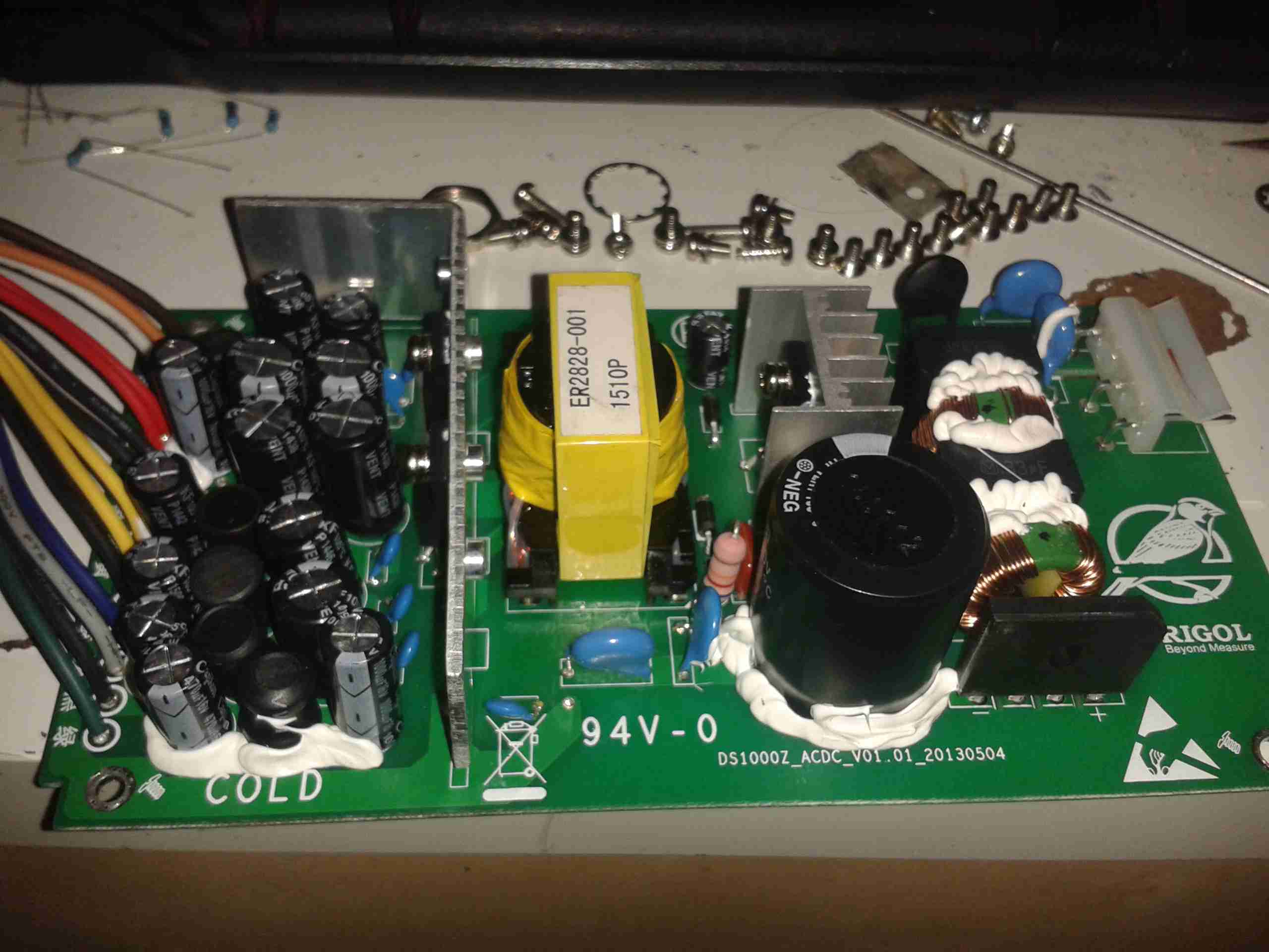
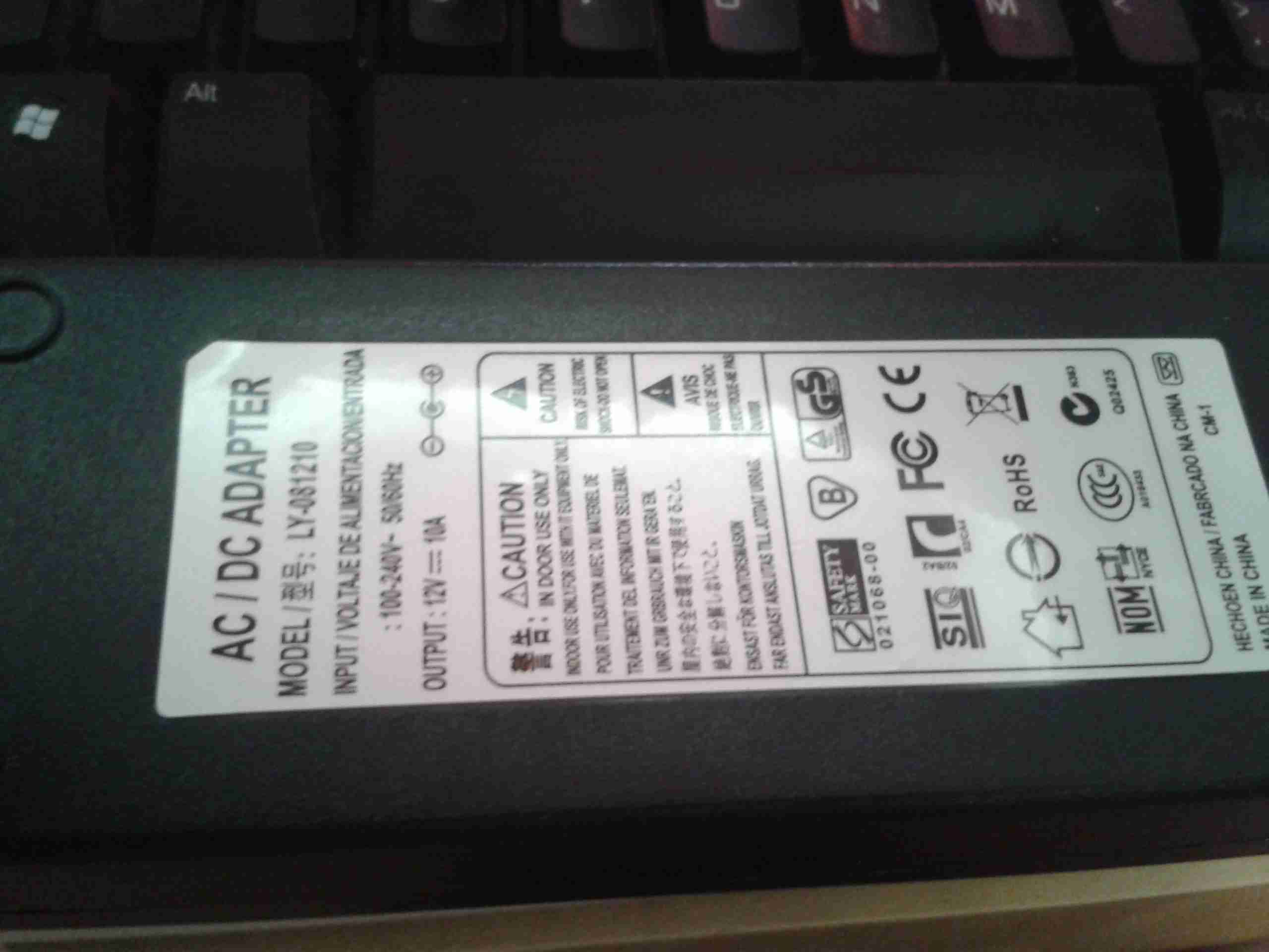
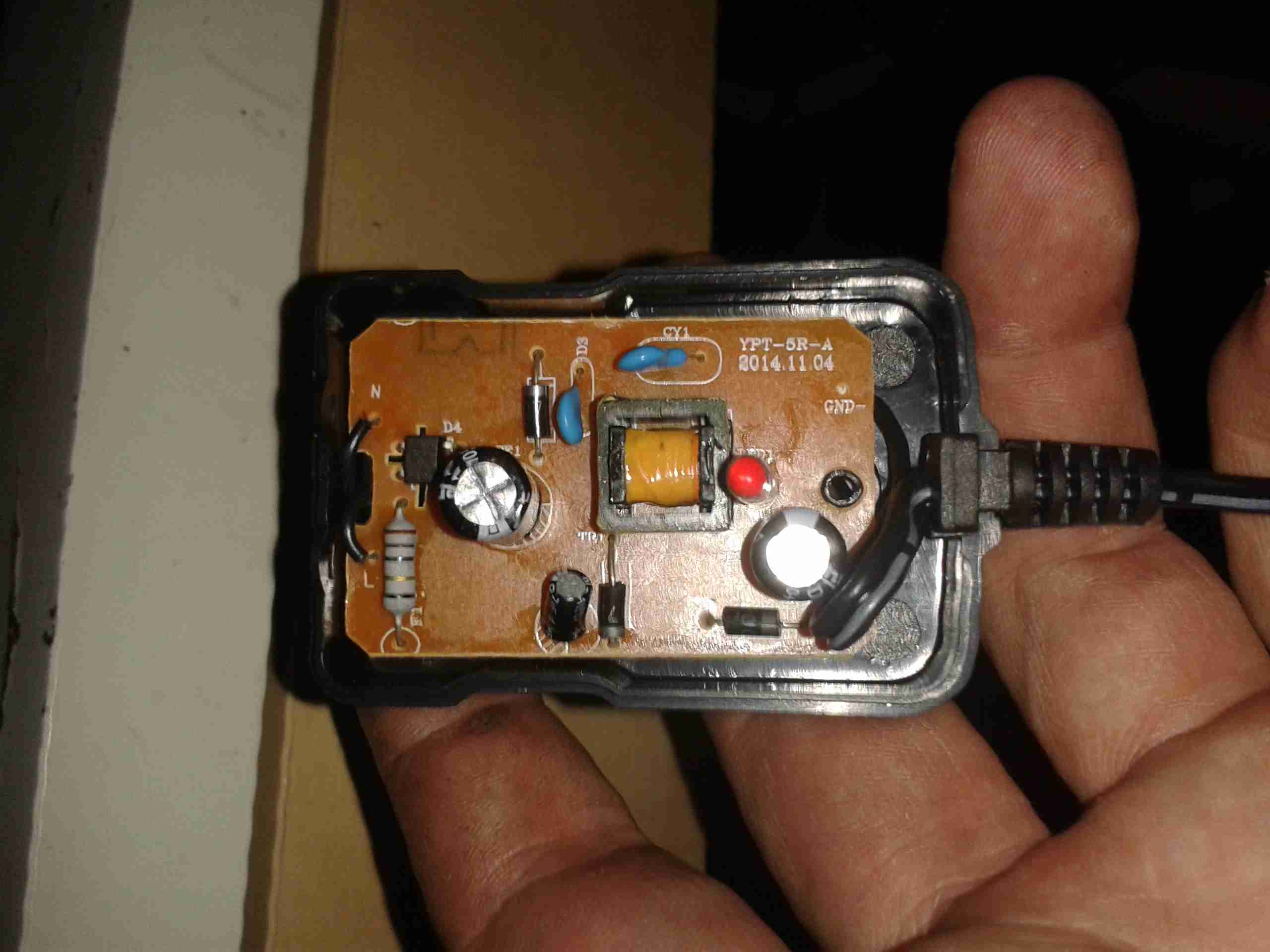
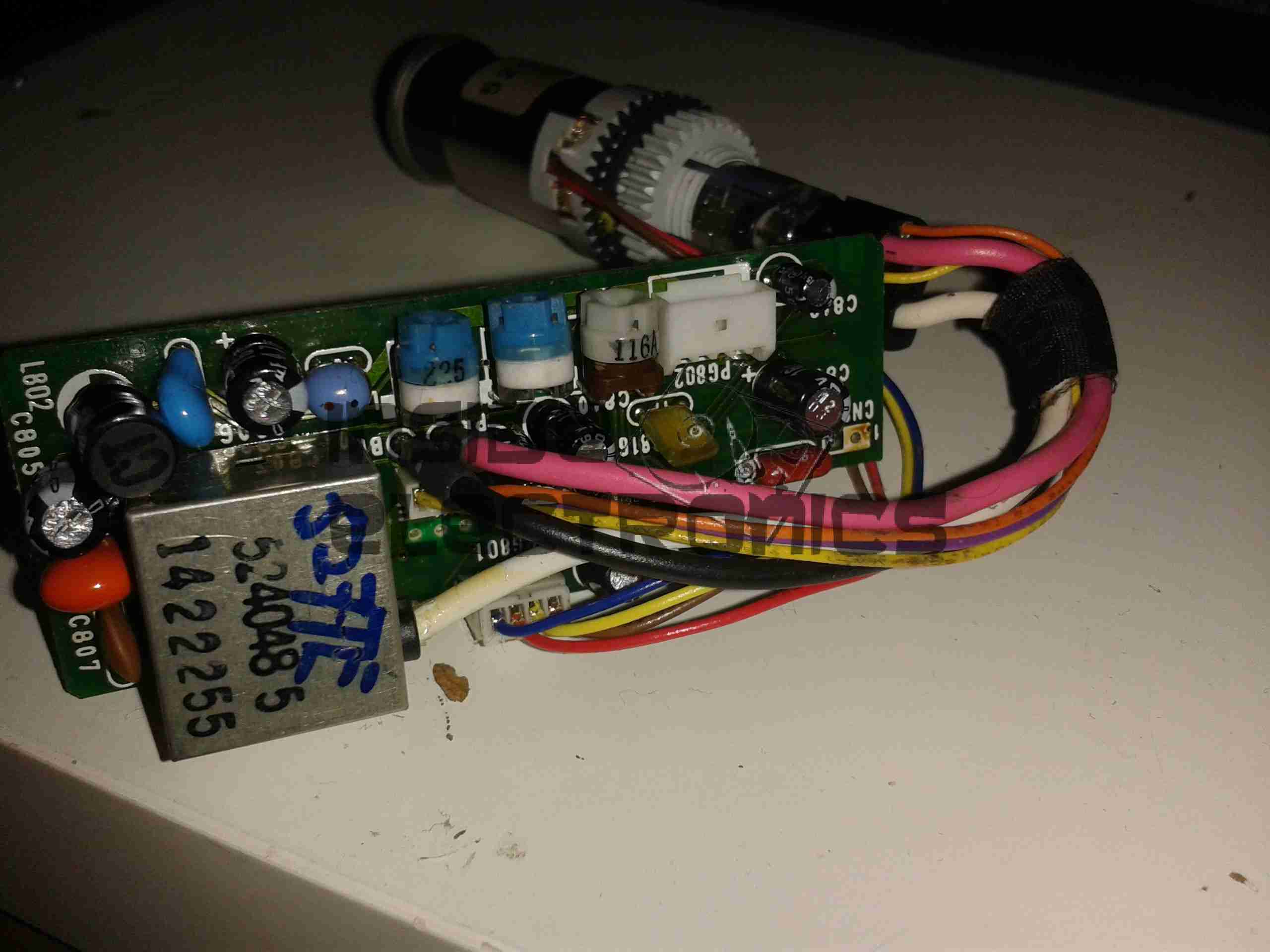
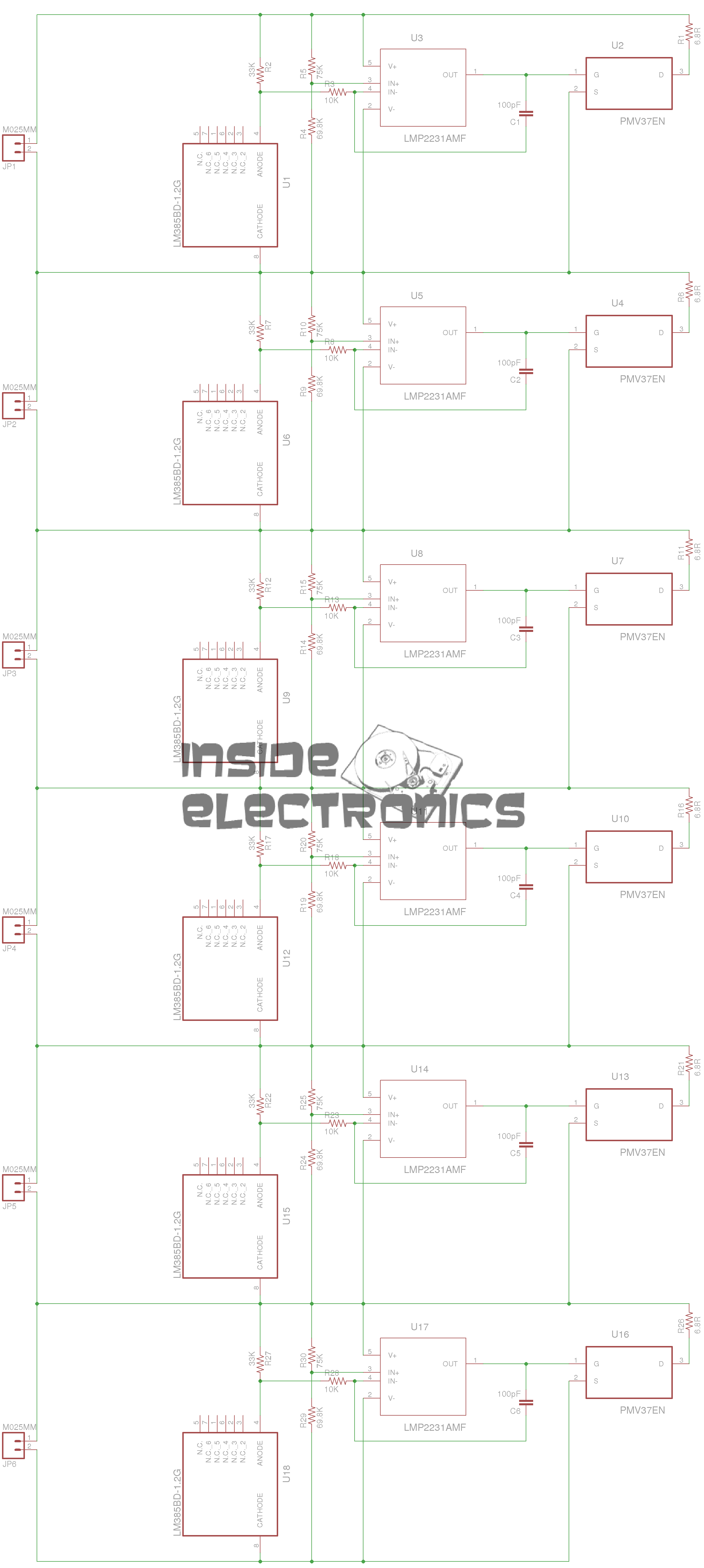
Here’s the factory mains SMPS unit from the back of the scope. This is a nice multi-rail unit, with several different outputs, the table below details the wiring of the PSU.

Connector PinPCB PinSignalMeasured VoltageMainboardRectifier RatingWire Colour
51AC_TRIGN/AAC_TRIGN/ABROWN
22+9v_GNDN/AFAN --NAORANGE
113+9V10.16VFAN +2AWHITE
64+5V5.1V5V5A20ARED
135+5V5.1V5V5A20ARED
76GNDN/AGNDN/ABLACK
87GNDN/AGNDN/ABLACK
38+7.5V6.9V6.3V20AYELLOW
109+7.5V6.9V6.3V20AYELLOW
110GNDN/AGNDN/ABLACK
121117.5V17.51V17.5V2ABLUE
912-17.5V-17.36V-17.5V2AGREY
1413GNDN/AGNDN/ABLACK
414-7.5V-6.84V-7.5V2AGREEN

The only feature I will lose if I make this switch is AC line triggering, but I never use that anyway, so it’s not a big issue for me.

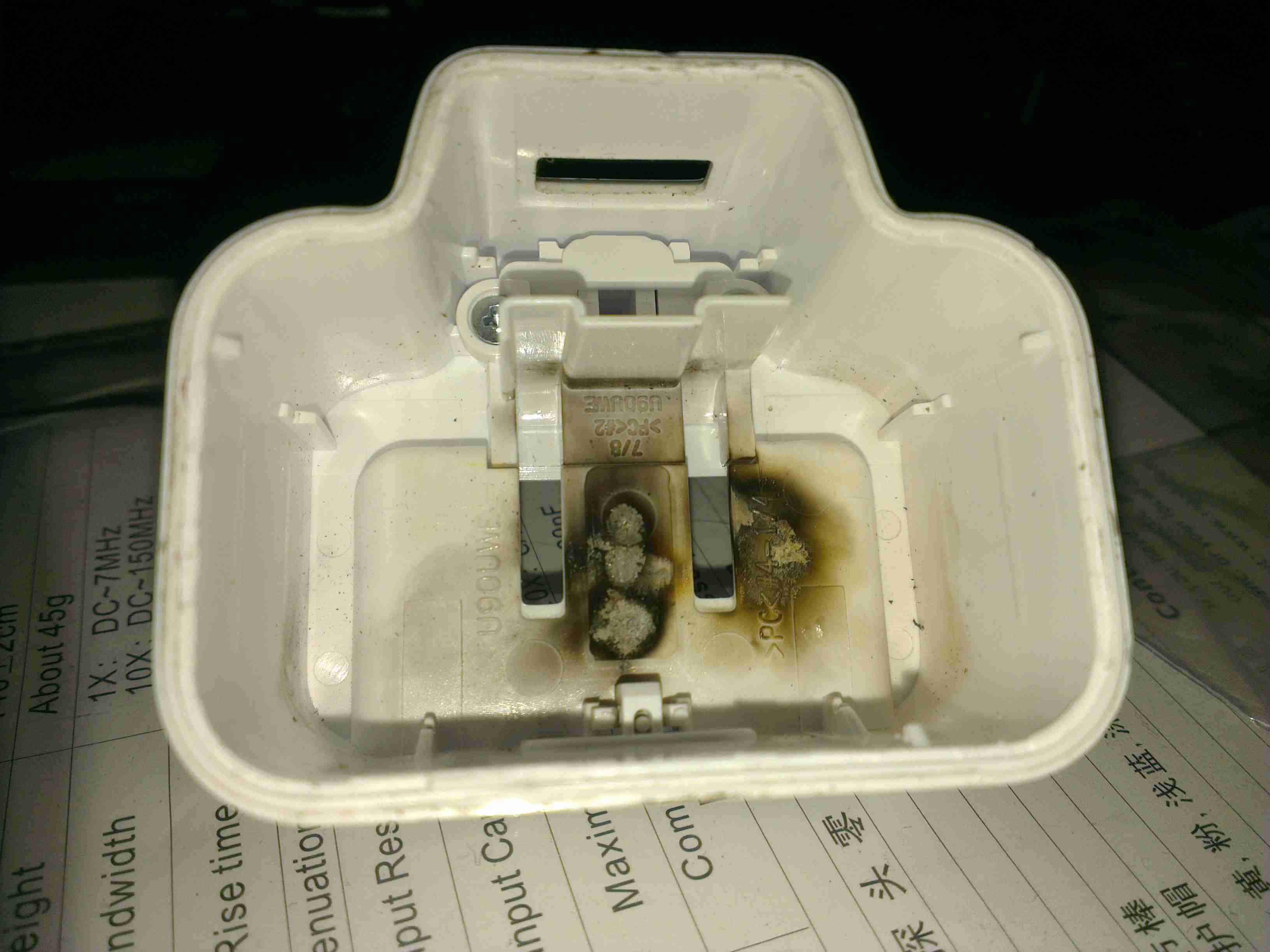
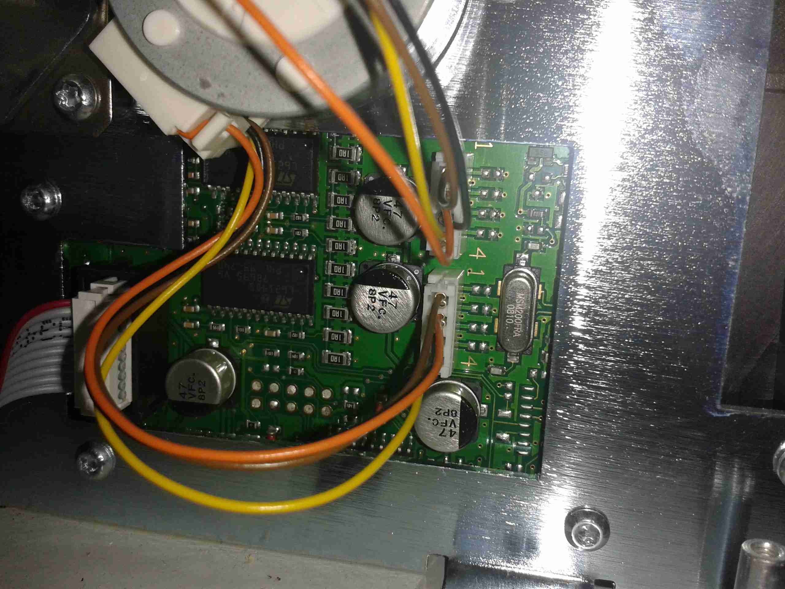
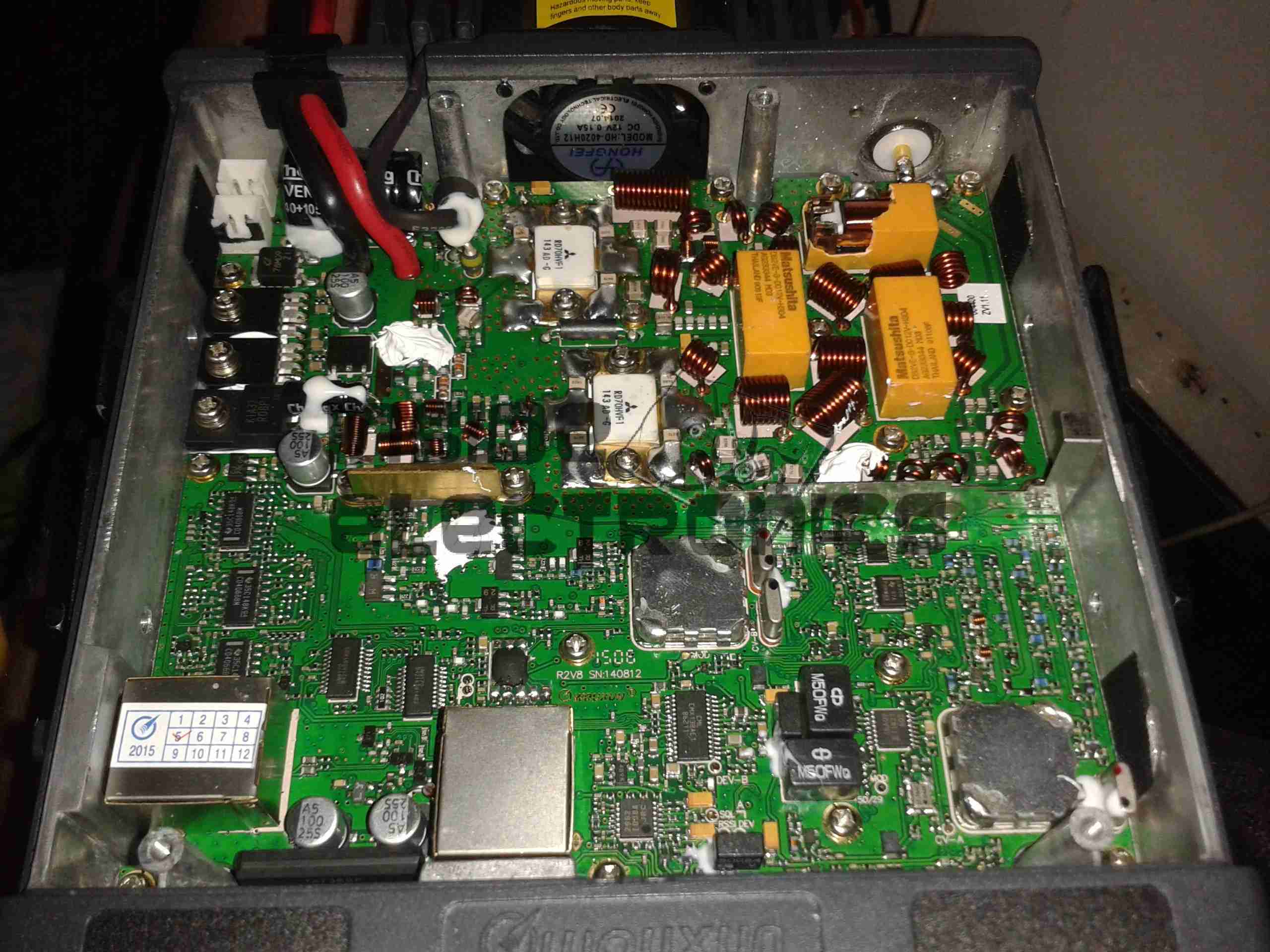
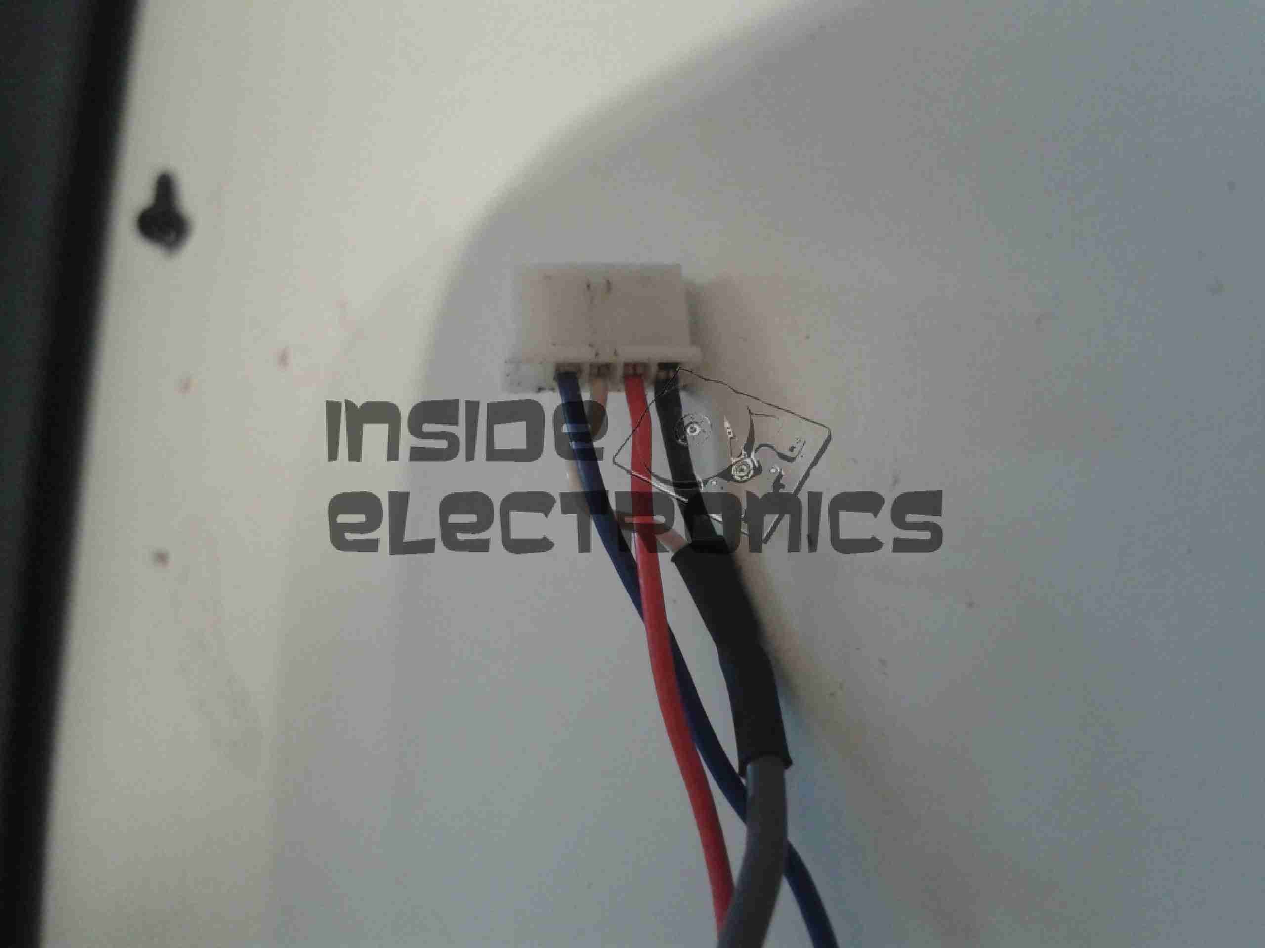
The connector used by Rigol to connect to the mainboard is a Molex Mini Fit Jr. Series 14-way type.

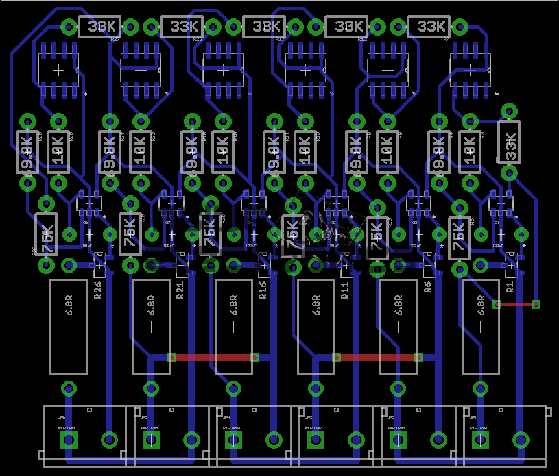
Since I have been able to locate the connector, the plan is to design a replacement low voltage supply unit for the scope, with the same footprint as the original AC mains supply. This will allow me to do a direct swap without causing any damage or modifying the original supply.
This method will allow me to swap the 240v supply back into the scope if I ever come to need it.

I’m planning to use the LTC3863 DC-DC Controller from Linear Tech to generate the negative rails, this will go down to -150v on the output, so it’s pretty much perfect to generate them.

PSU Output Side
PSU Output Side

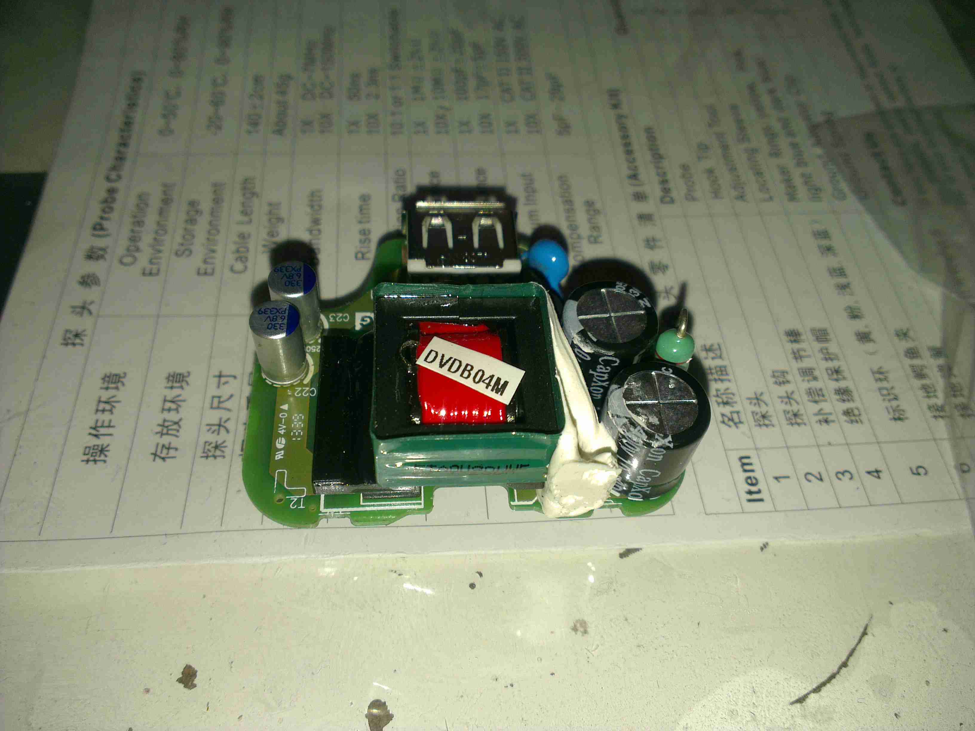
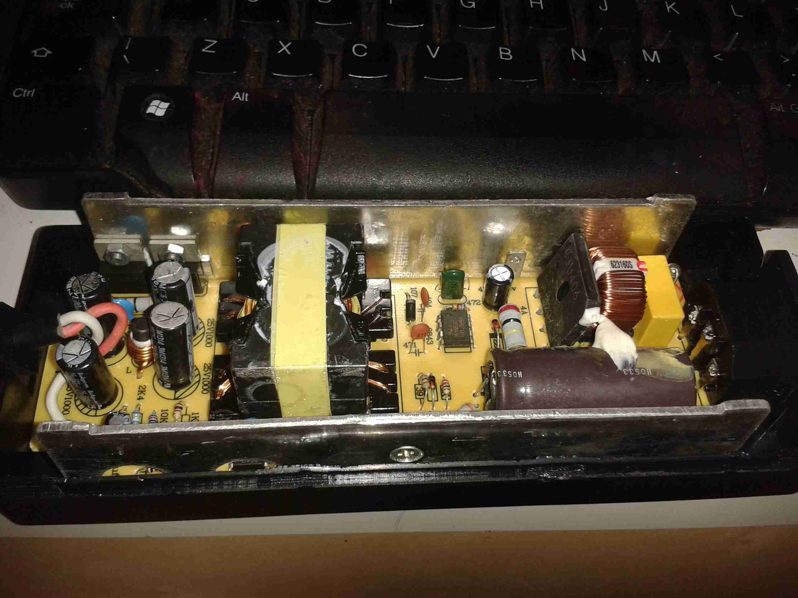
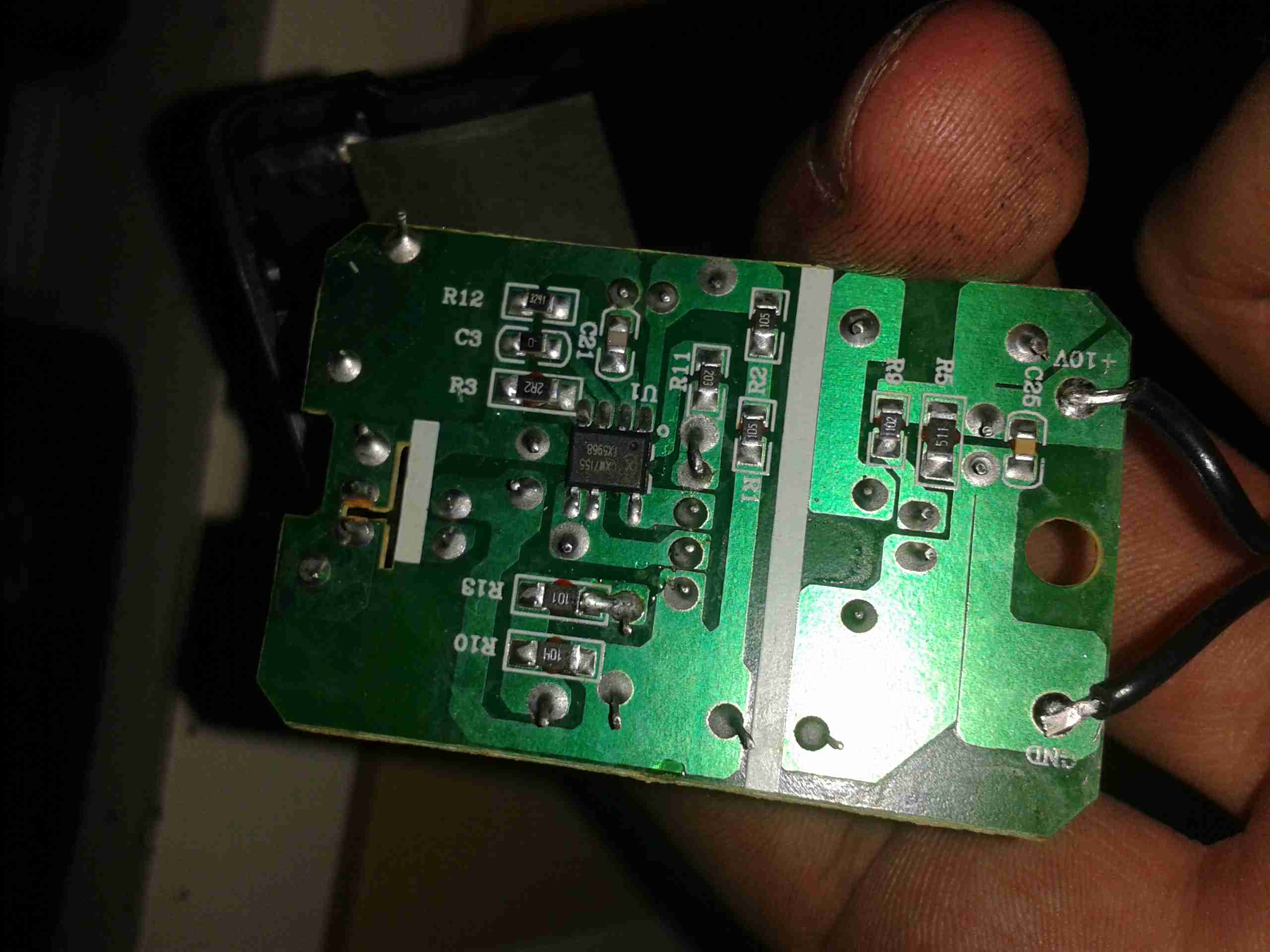
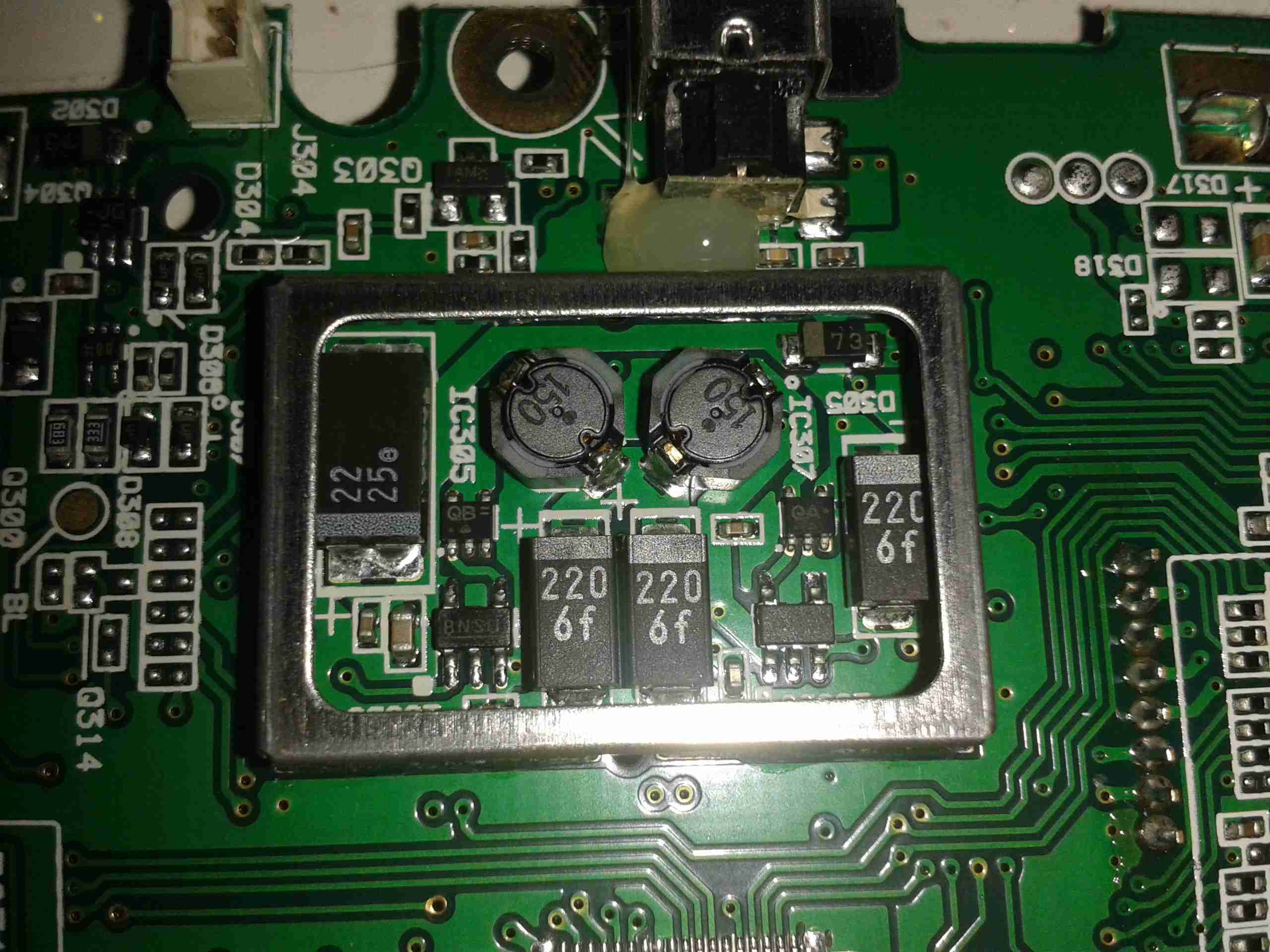
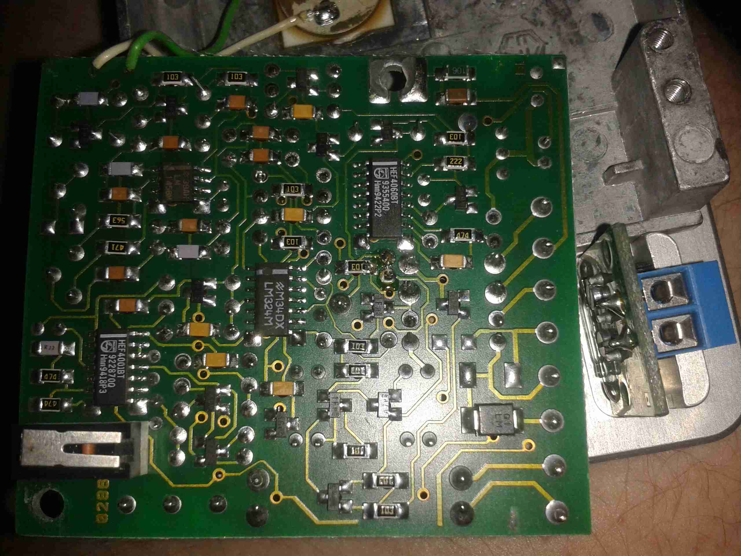
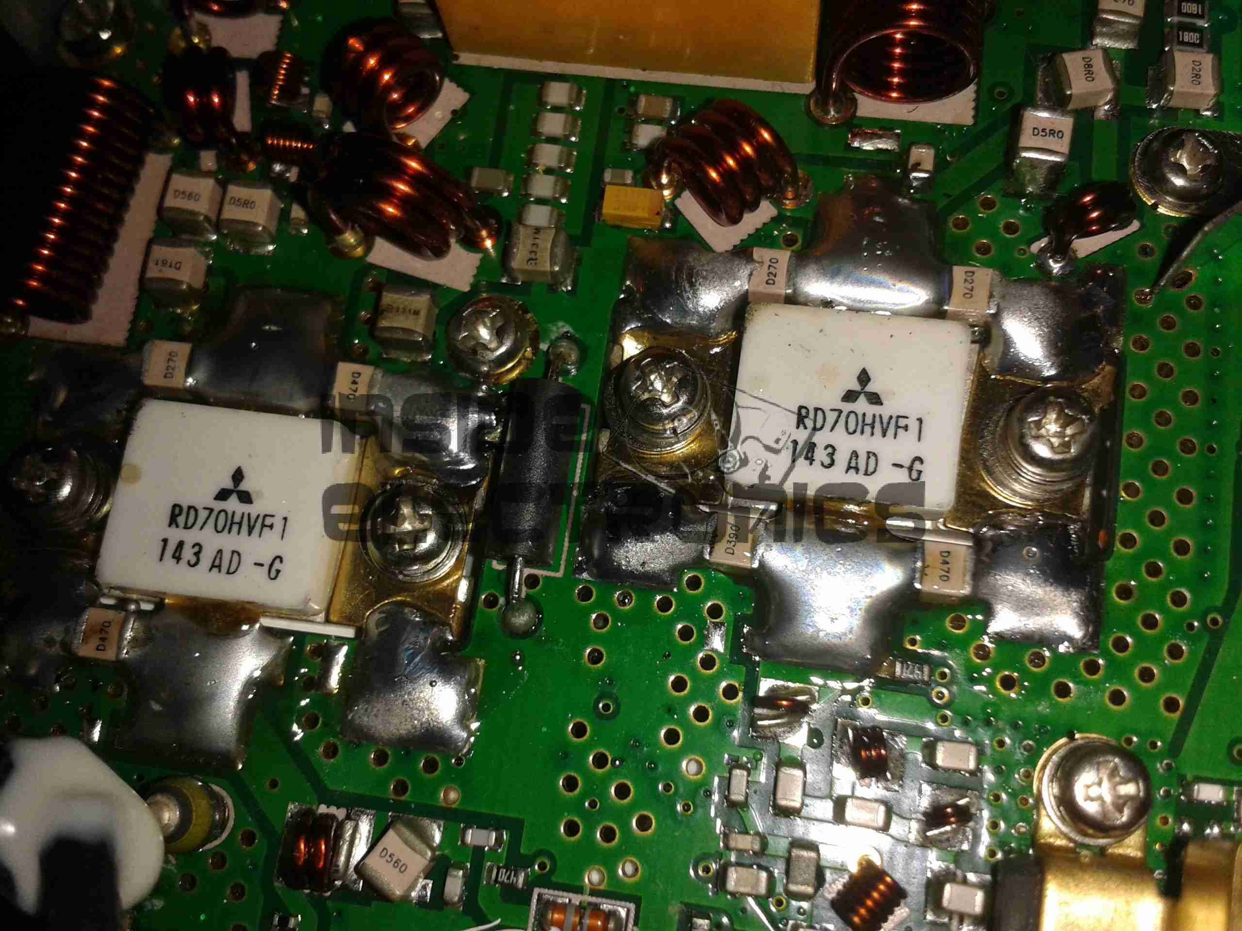
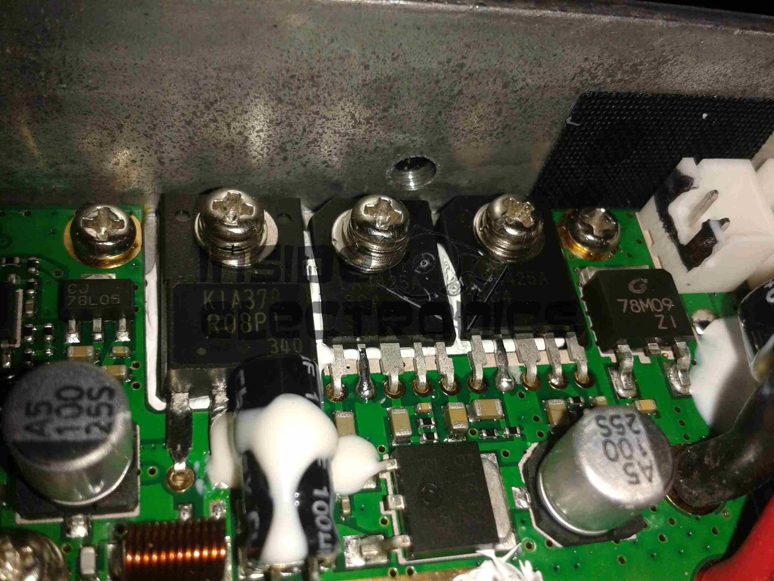
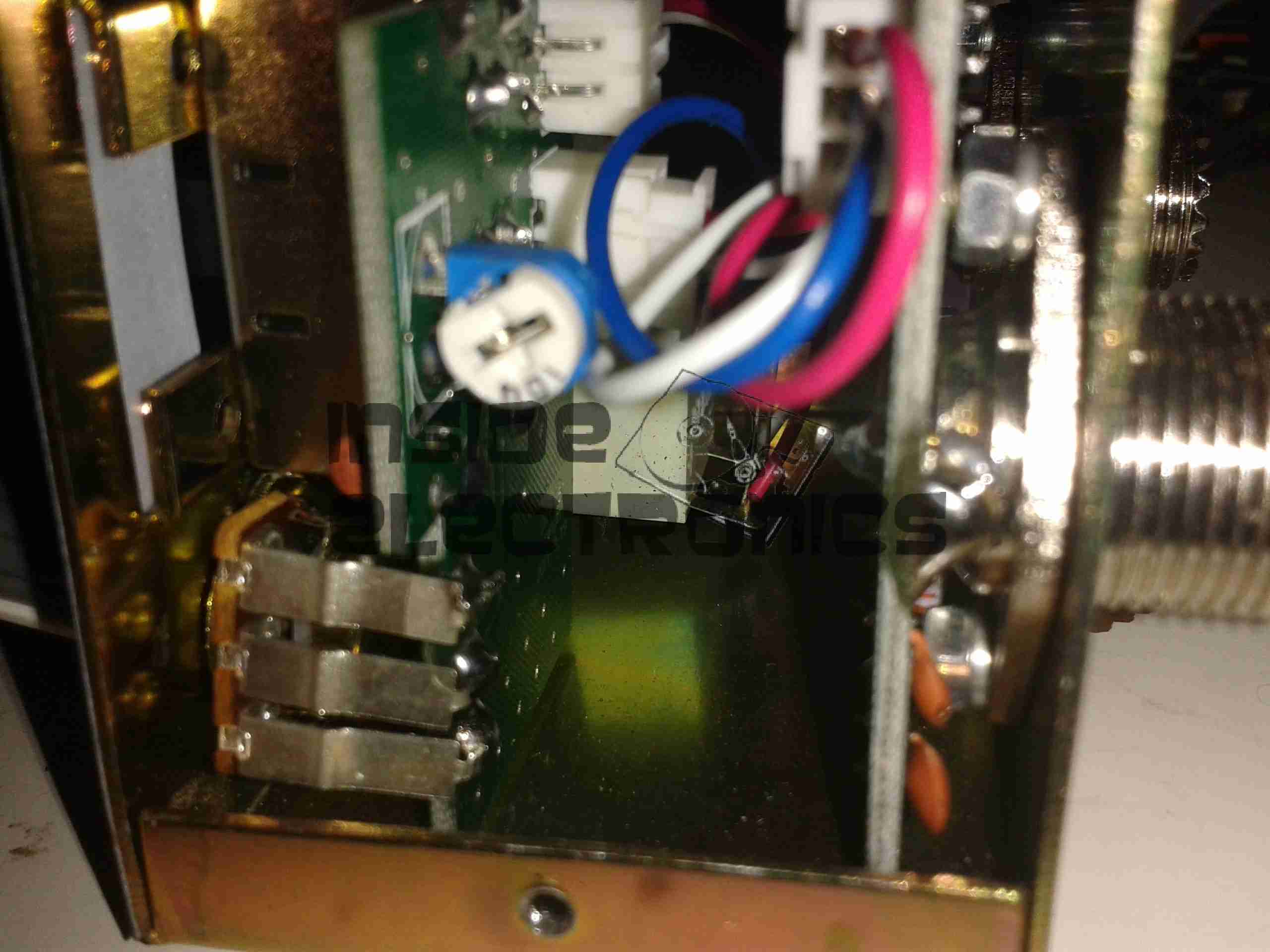
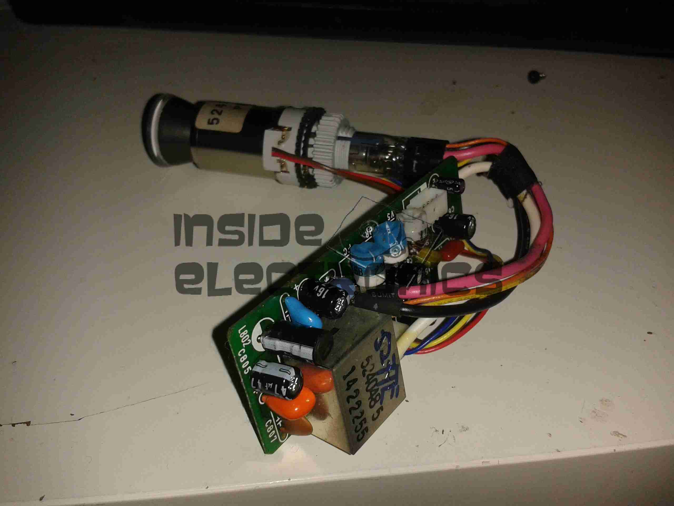
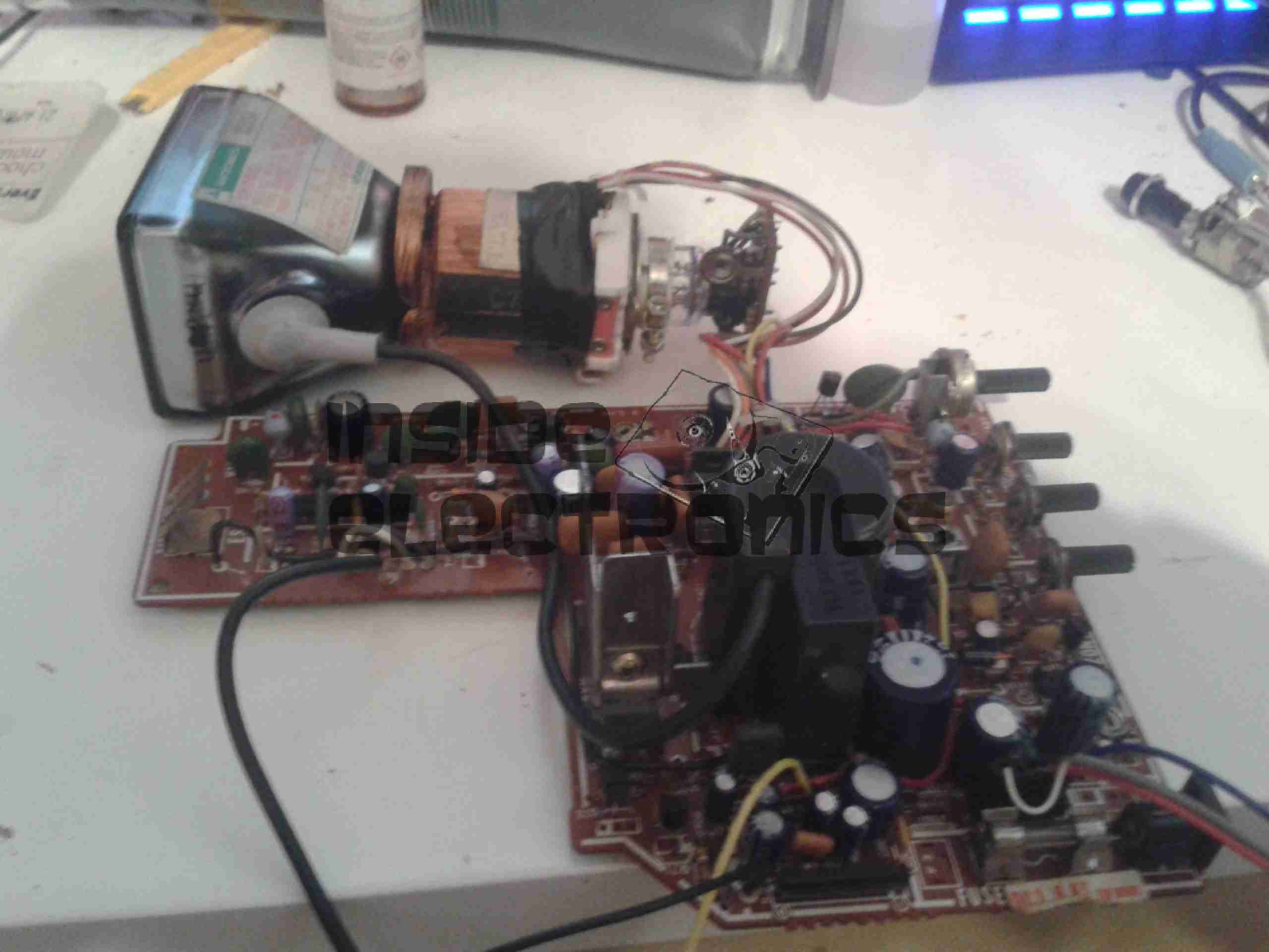
Here’s the output side of the mains PSU, it has a lot of filtering on the output rails, the two TO220 devices are the output rectifiers for the +5v & +7.5v rails, these are rated at 20A, 60V.

PCB Bottom
PCB Bottom

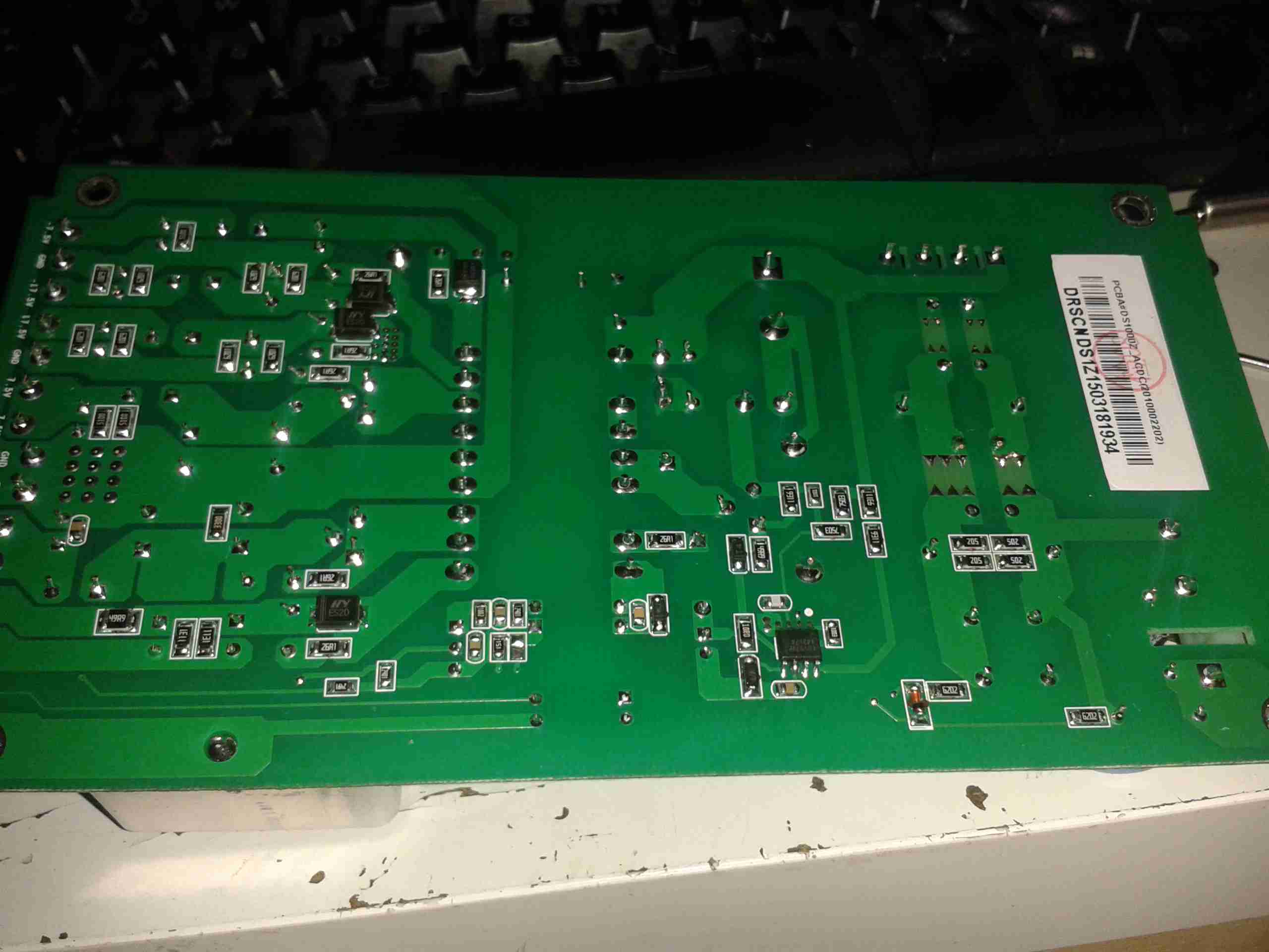
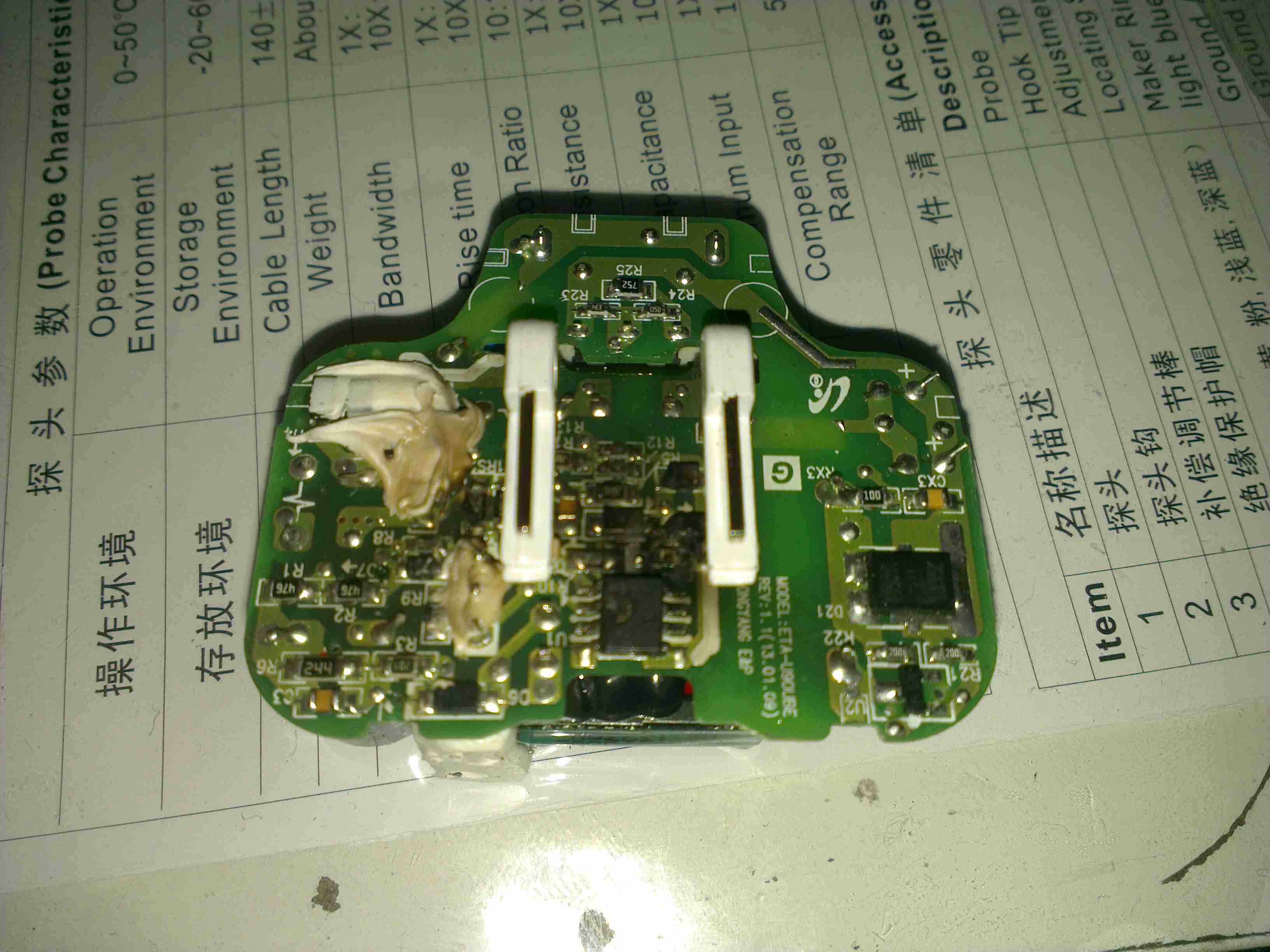
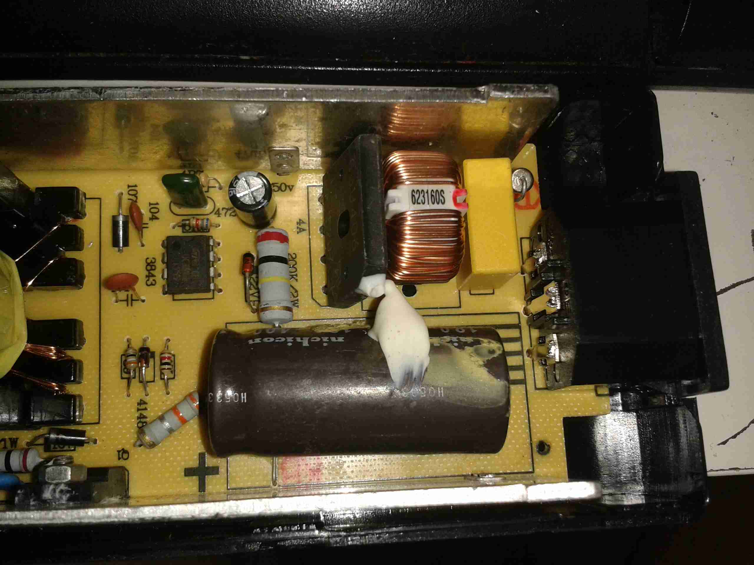
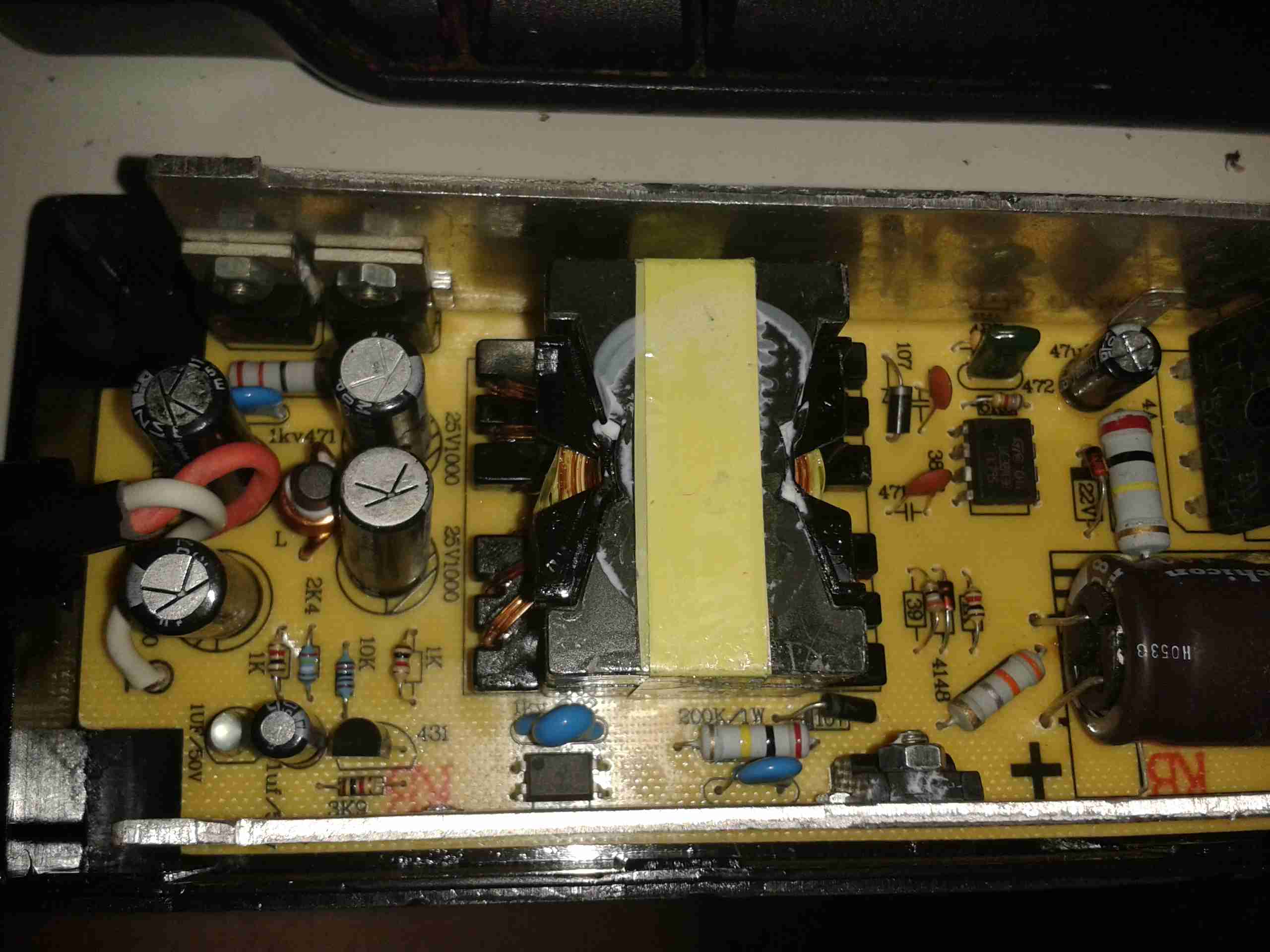
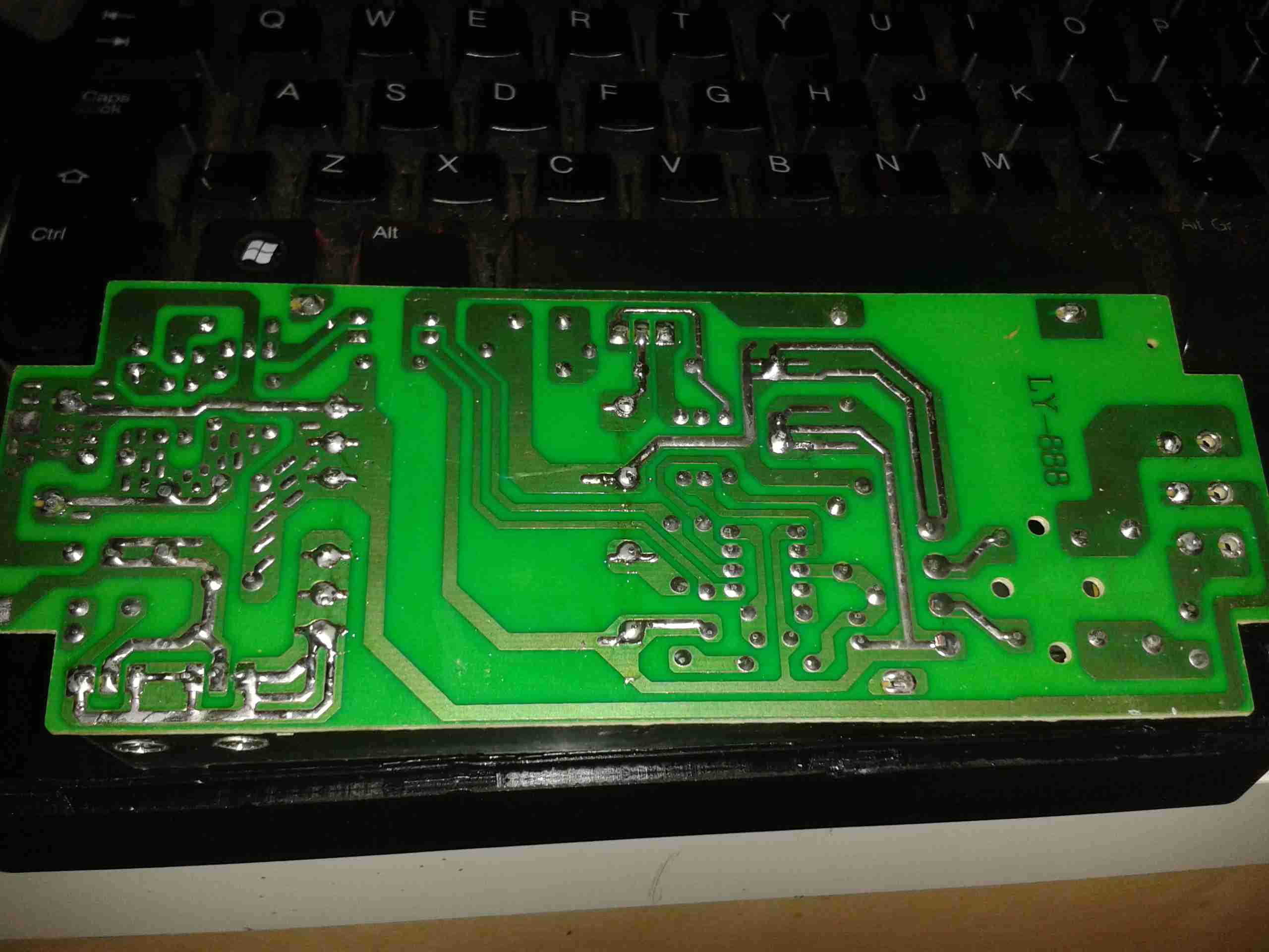
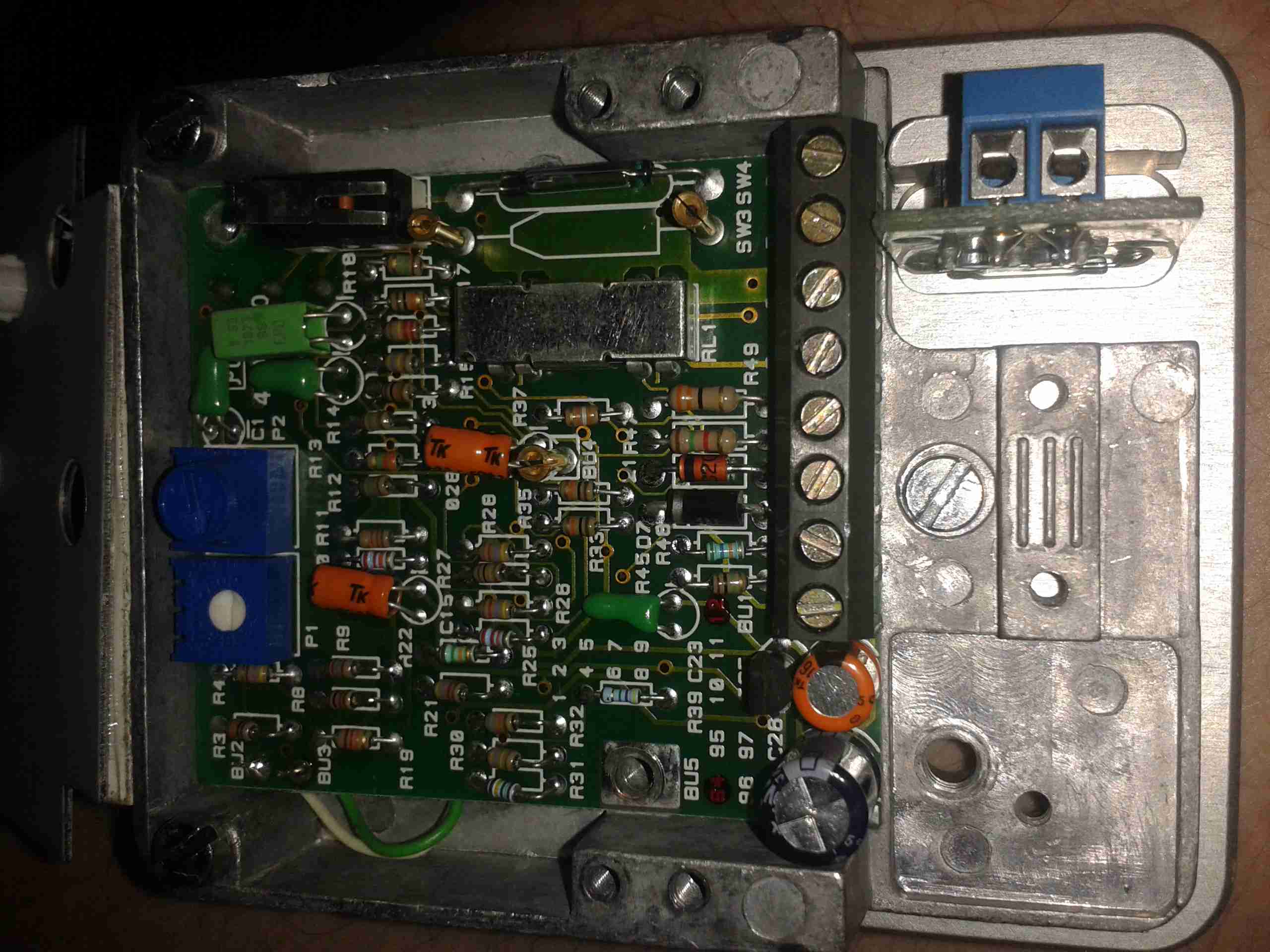
Here’s the bottom side of the PCB. It’s a really nicely designed PSU, massive isolation gap, spark gaps on the primary side & good filtering. The output side on the left has the rectifier diodes for the other voltage rails, these are only 2A rated, so designing the inverting supply to generate the negative rails will be pretty easy.

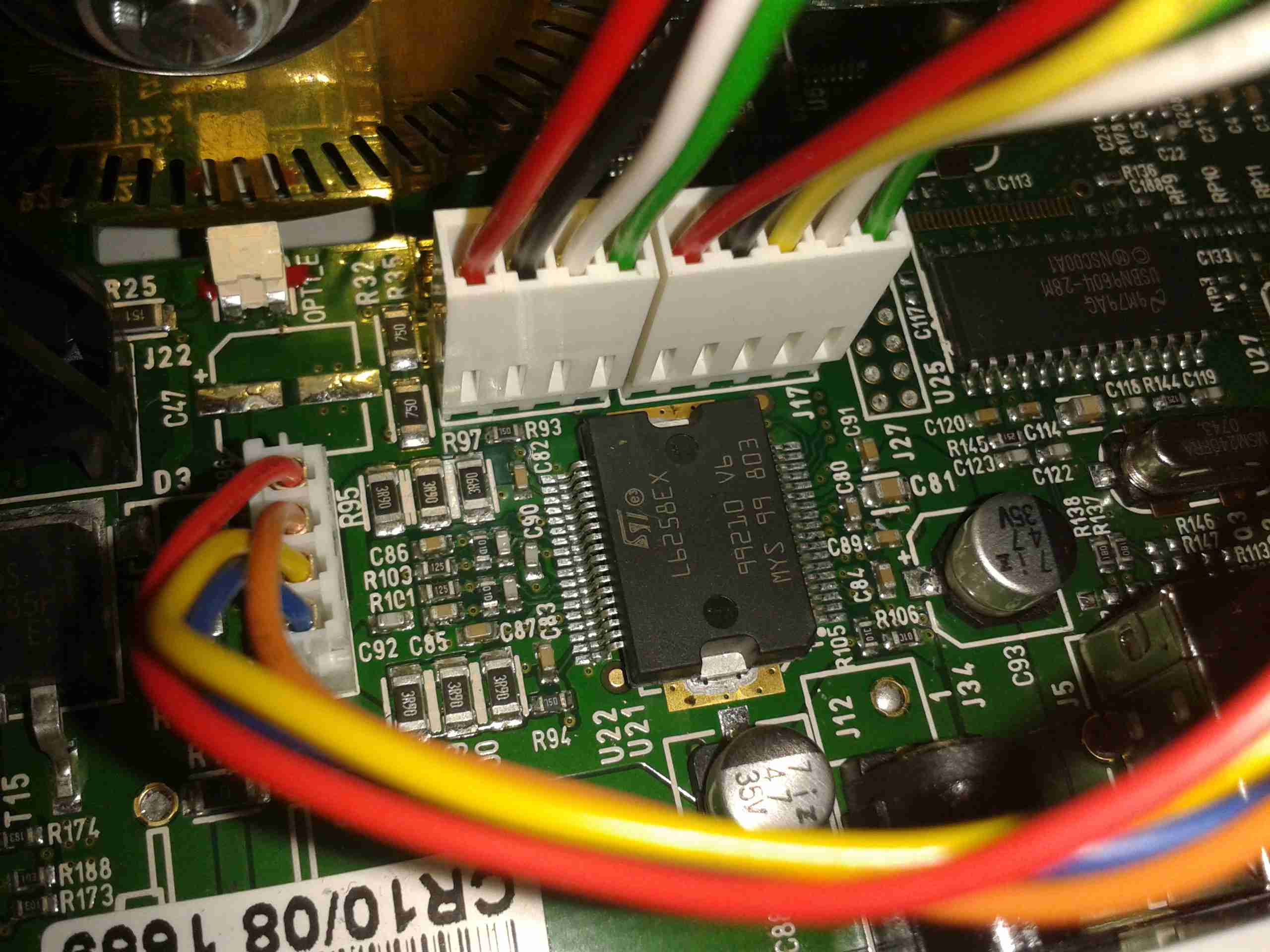
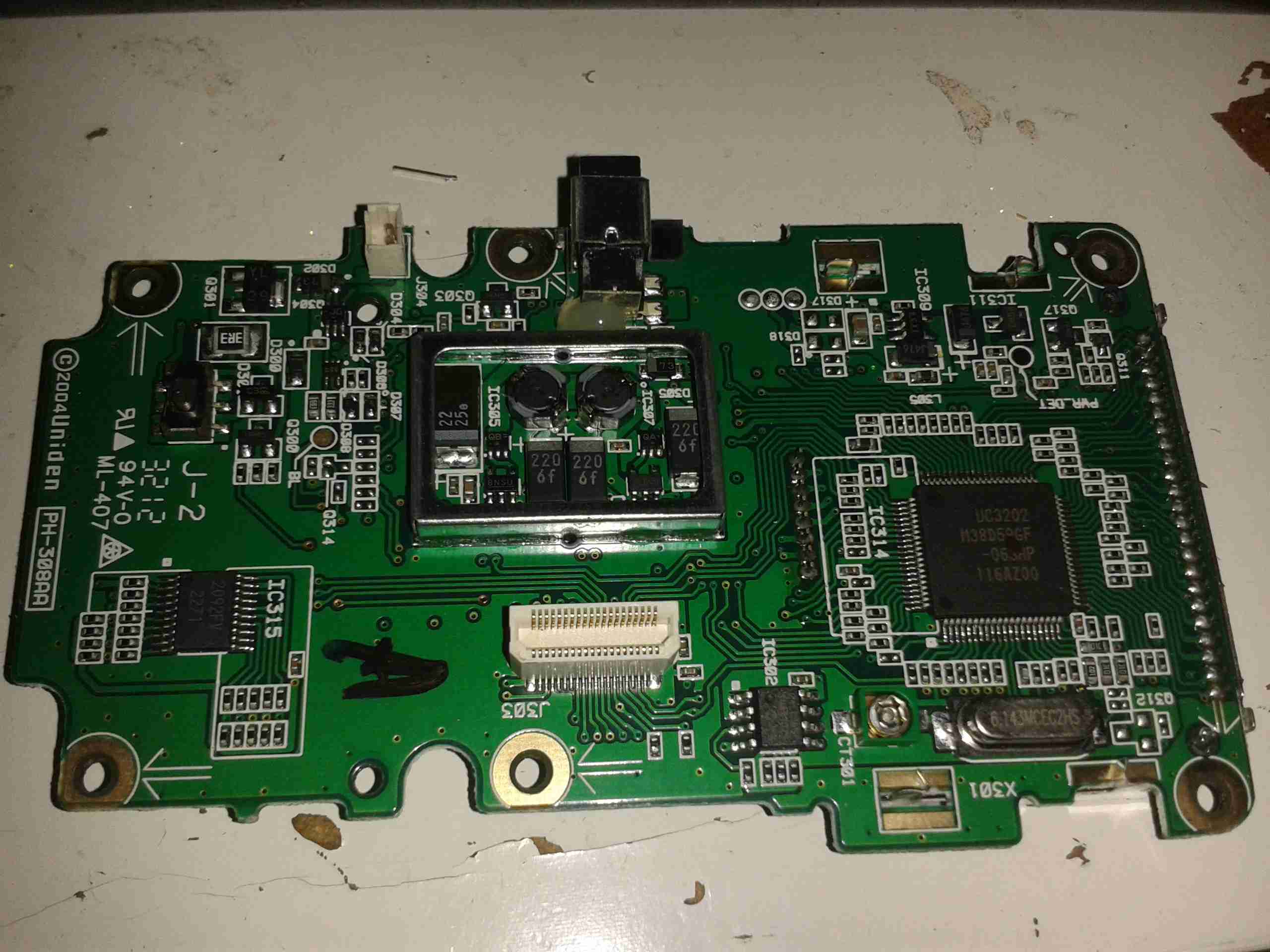
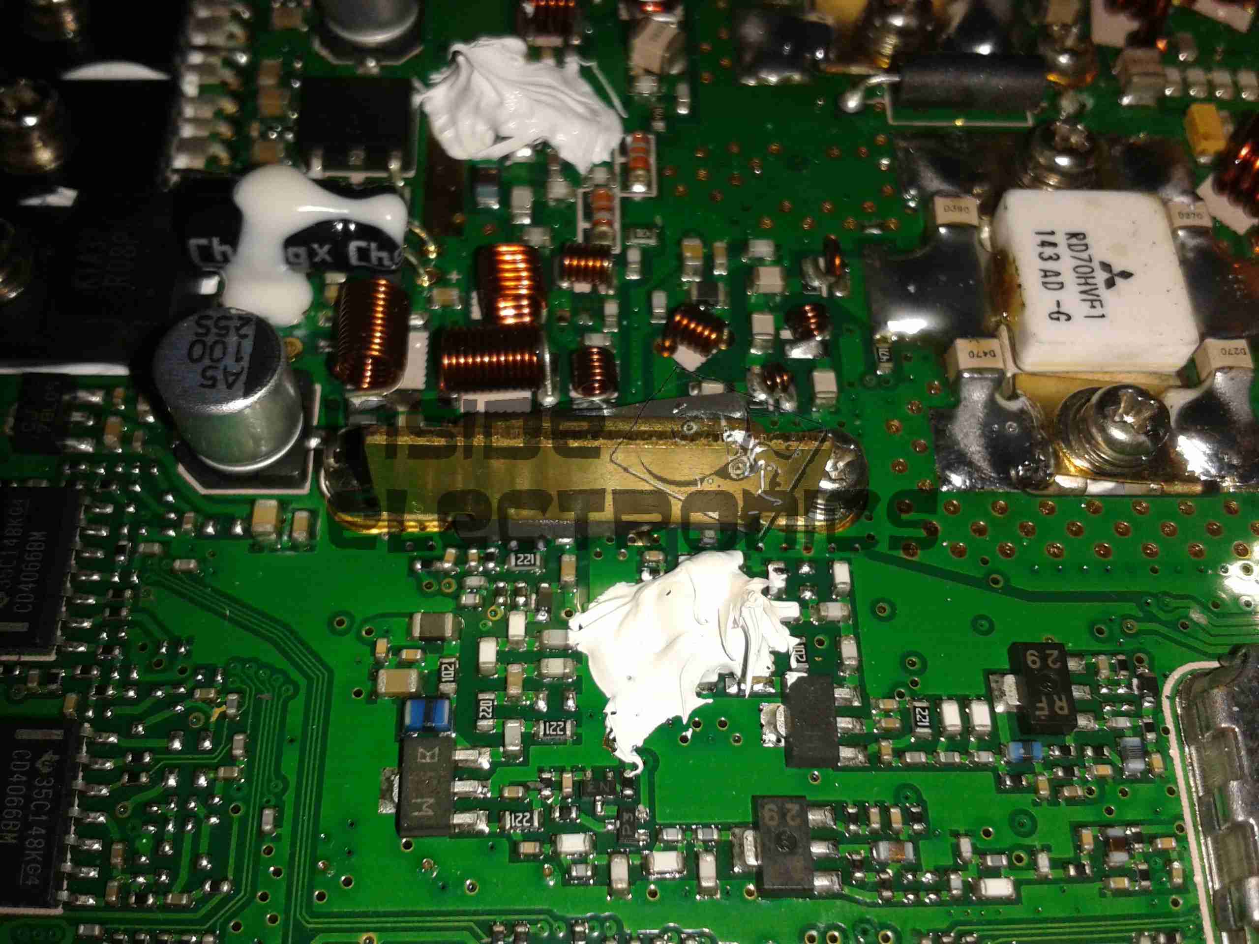
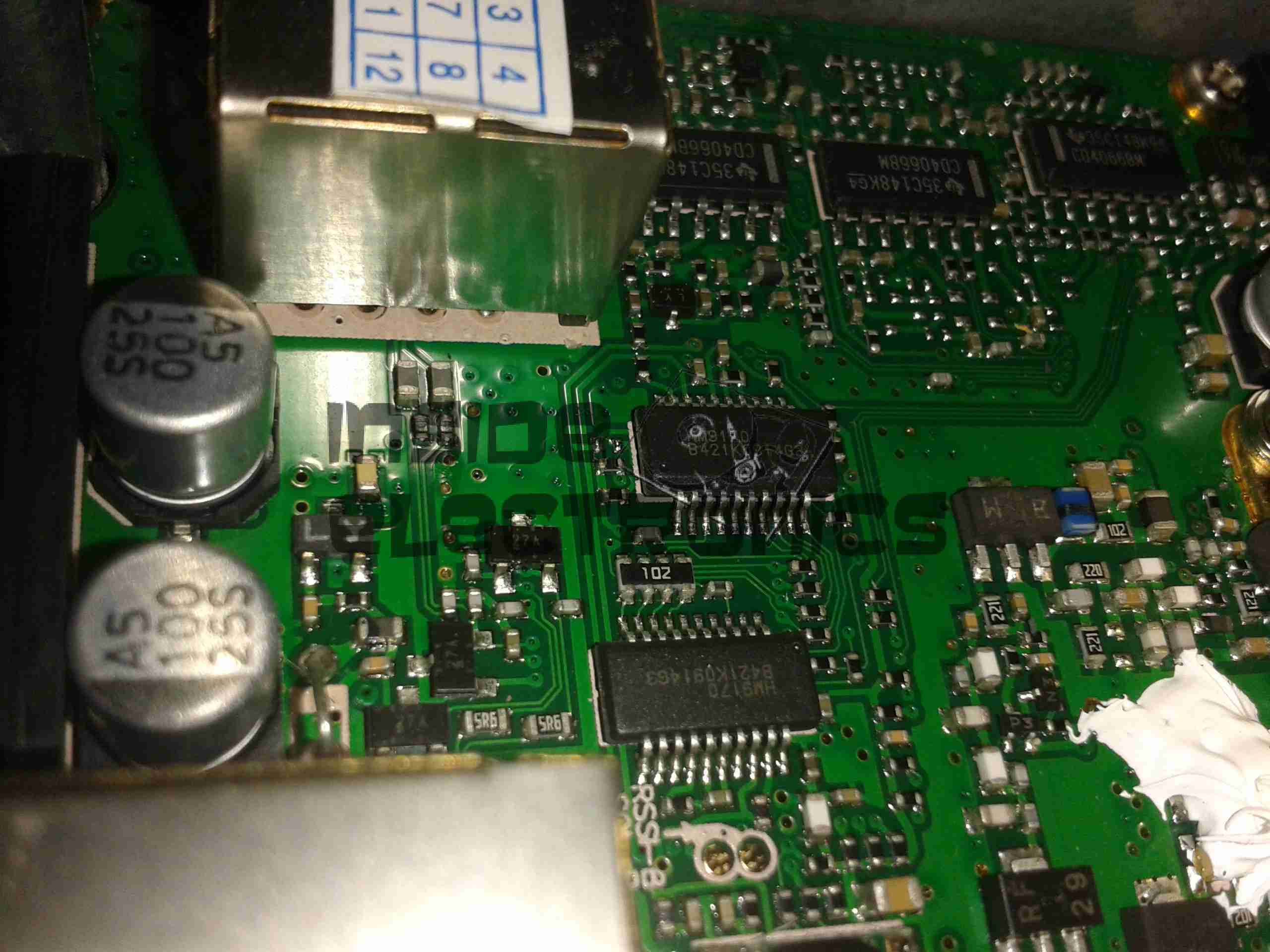
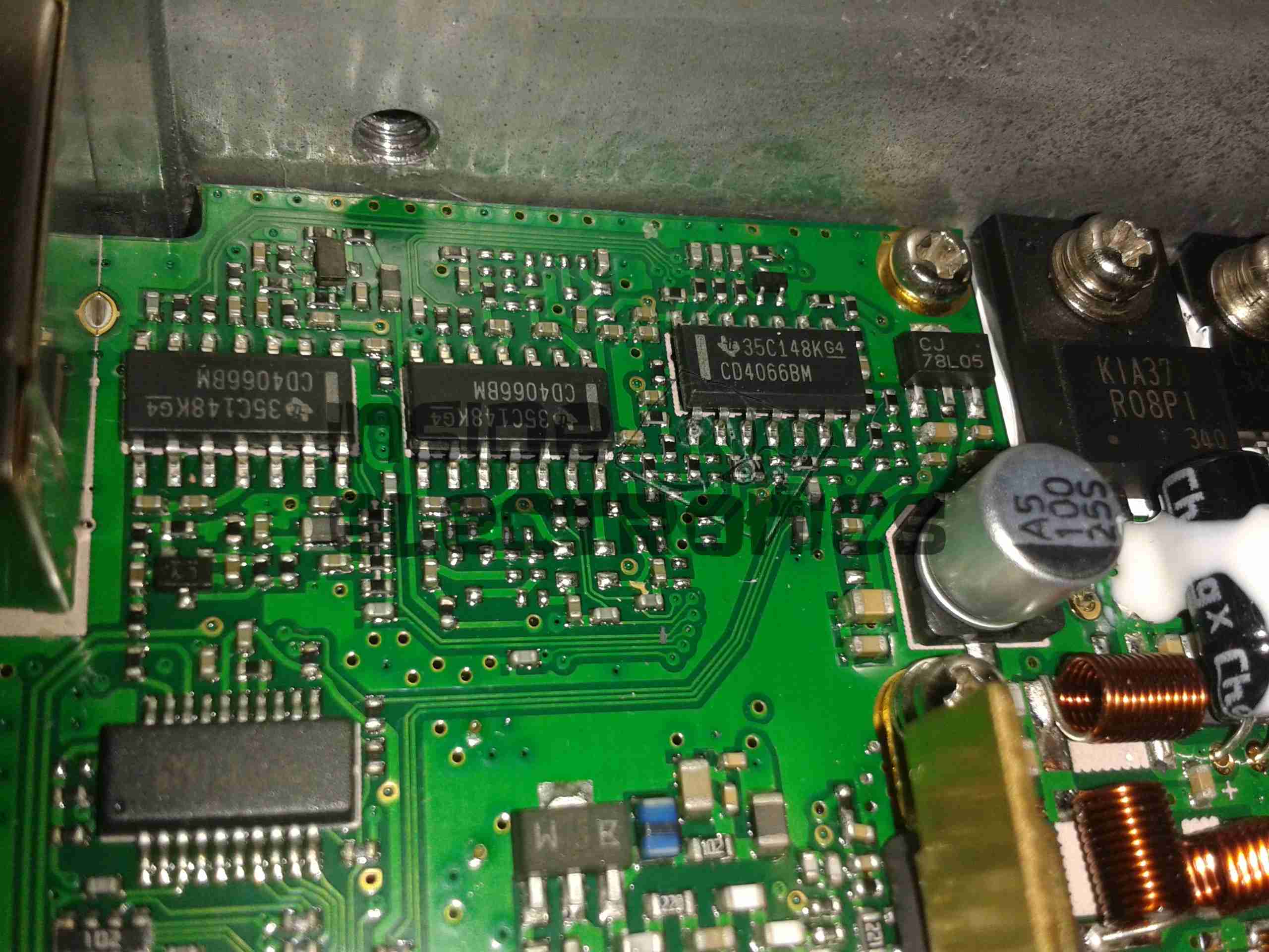
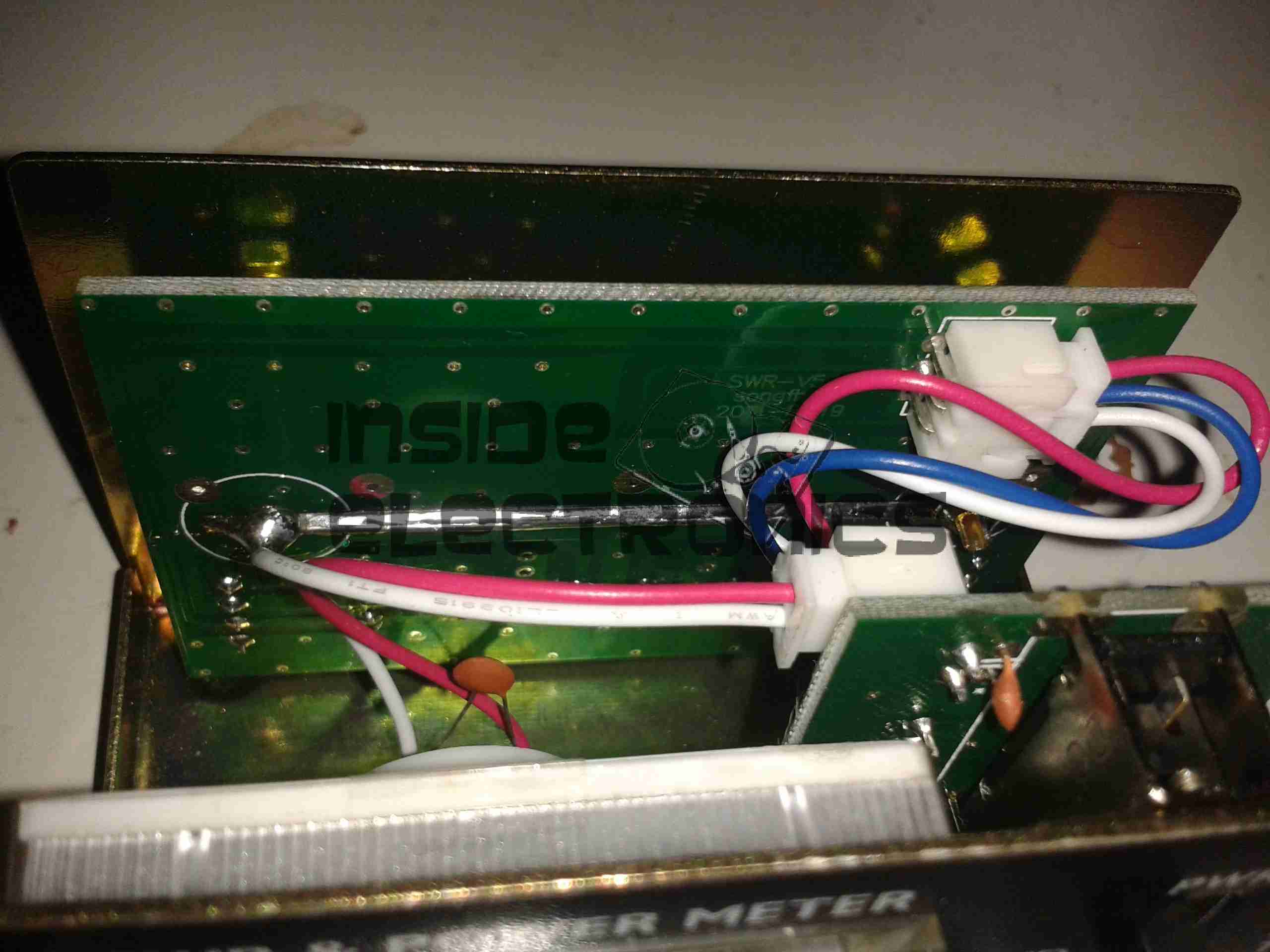
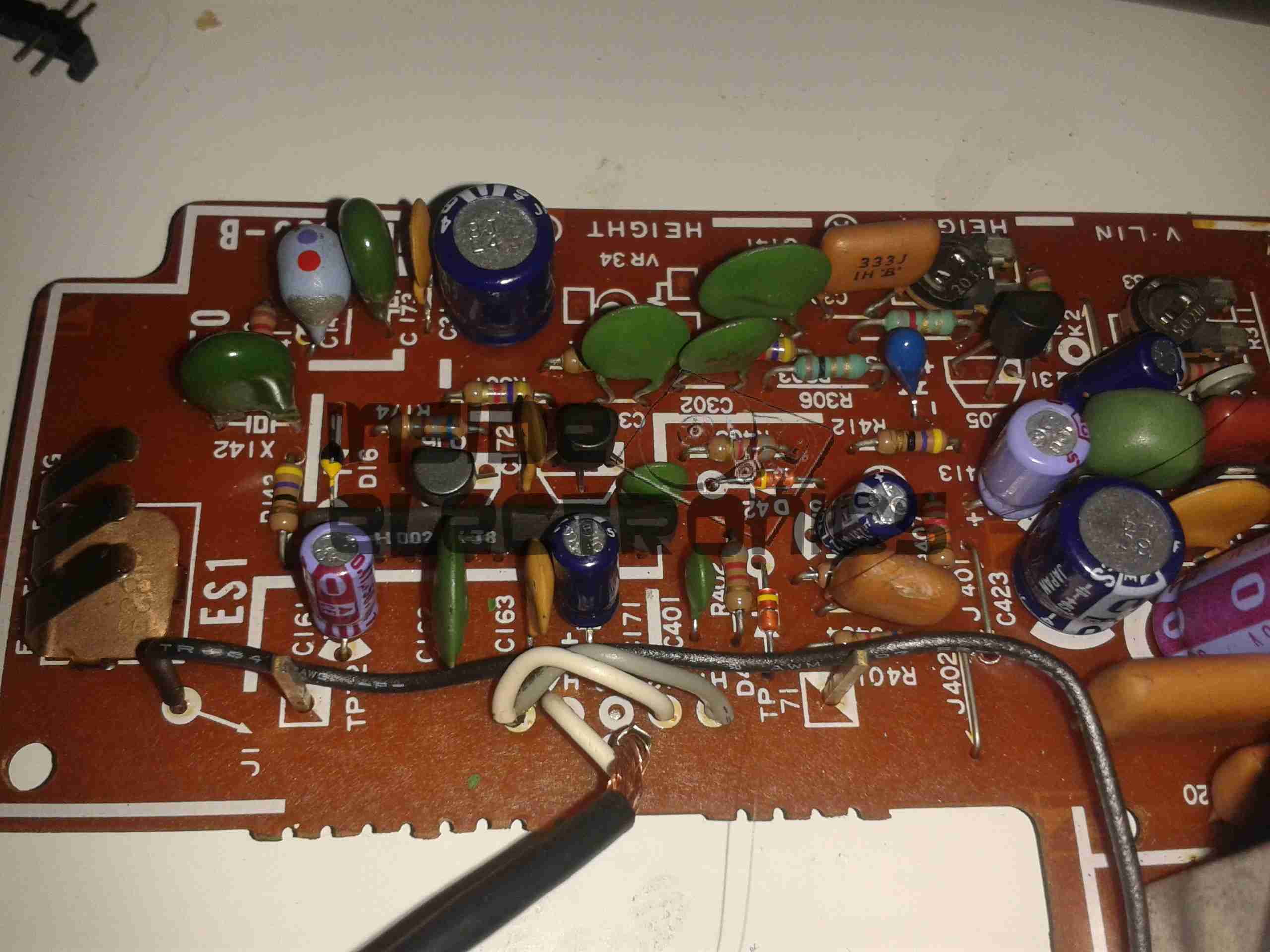
From looking at the PCB markings on both the mainboard & the PSU, the +9v rail seems to be used to drive the fan, both silkscreen markings indicate this.
The voltages marked on the PSU & the mainboard connector don’t quite match up though, there’s a small variation in the stated voltage between the two. This is most likely because all of the regulation of the supplies seems to be done on the mainboard, there are several linear regulators, and a few DC-DC switchers. Providing that the replacement supply isn’t noisy it should work fine.

This is backed up by the fact that the mains PSU only seems to regulate the +5v rail – on measuring the rails that’s the only one that’s close to spec.

Mainboard Power
Mainboard Power

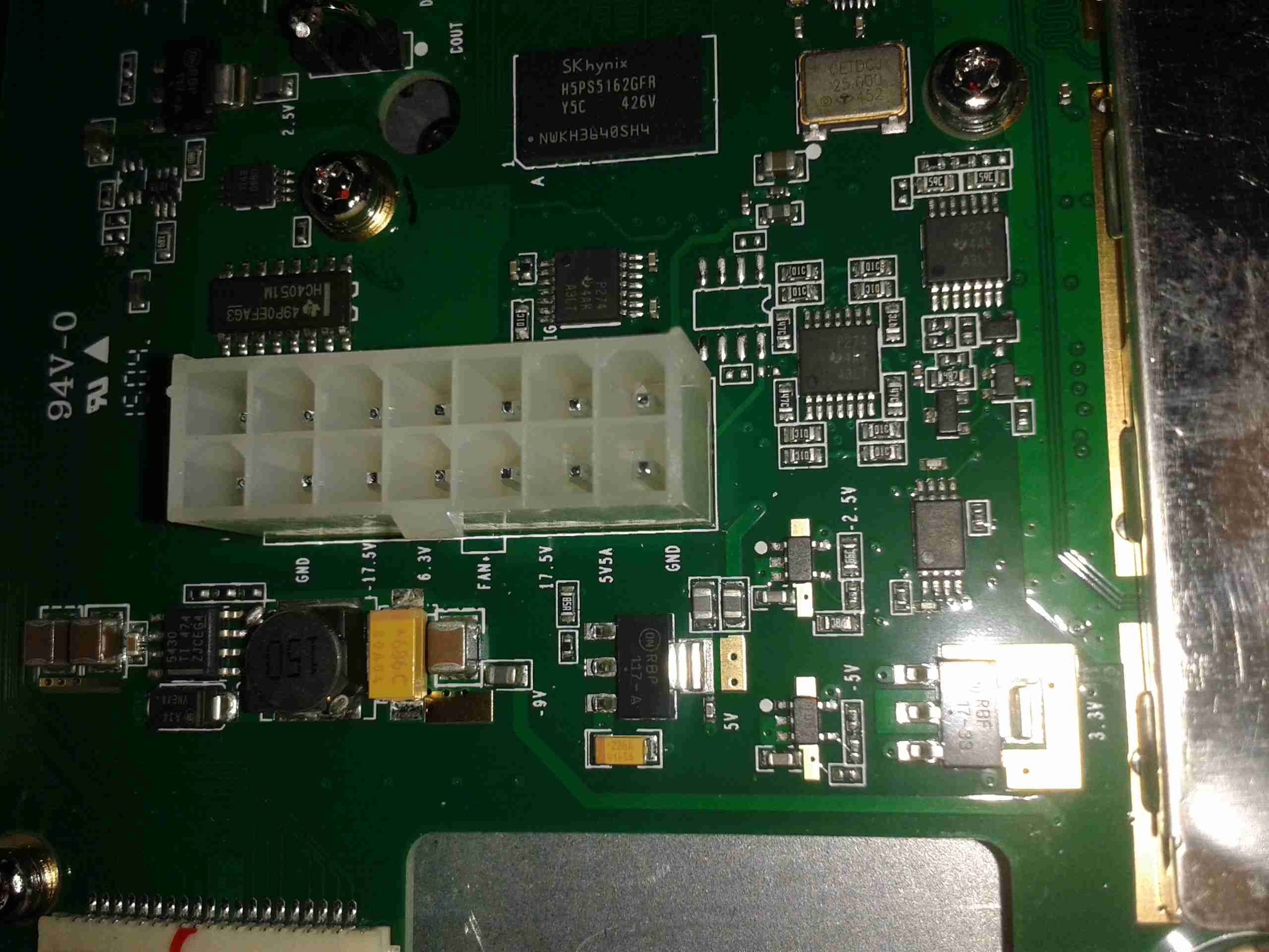
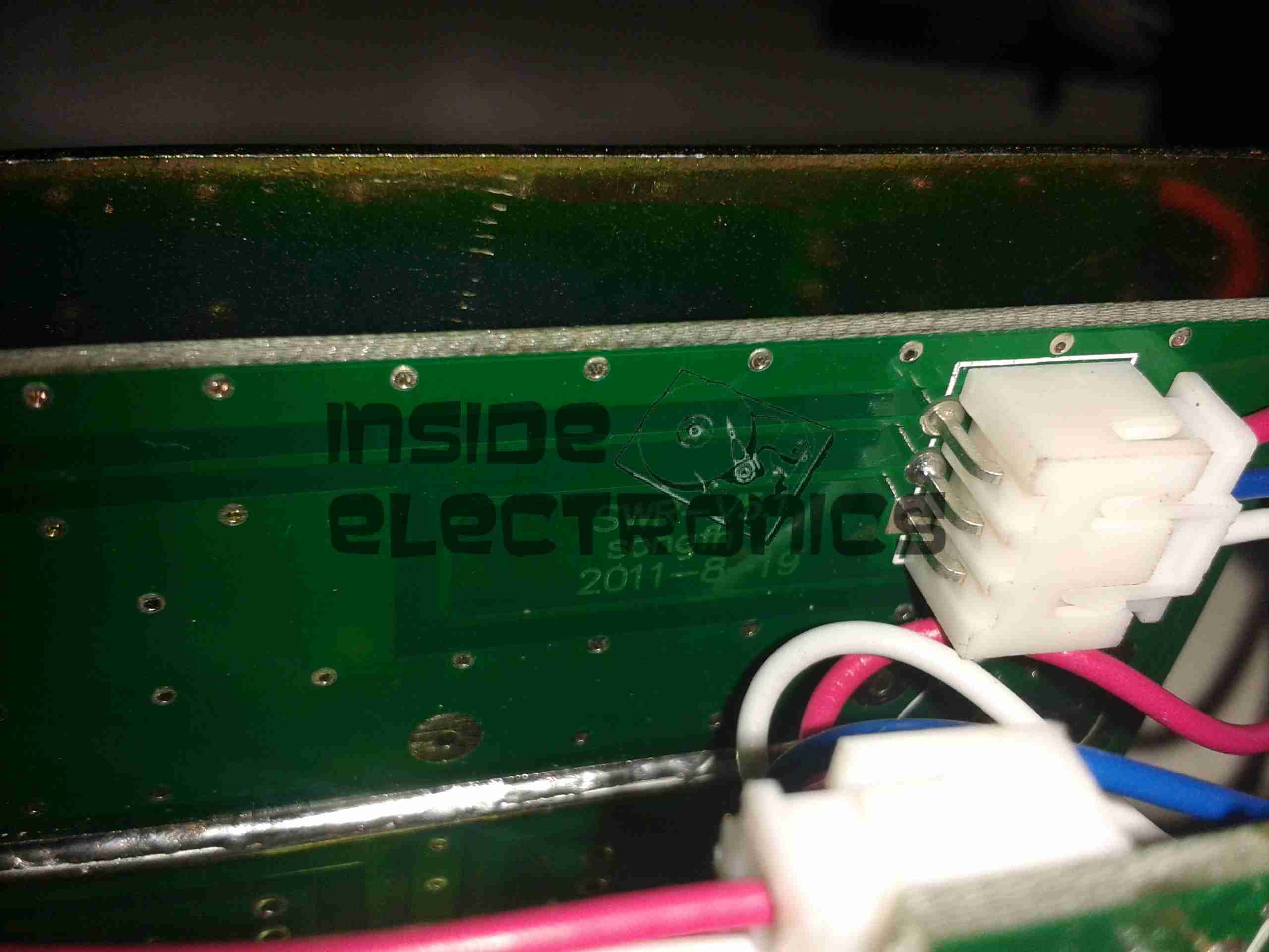
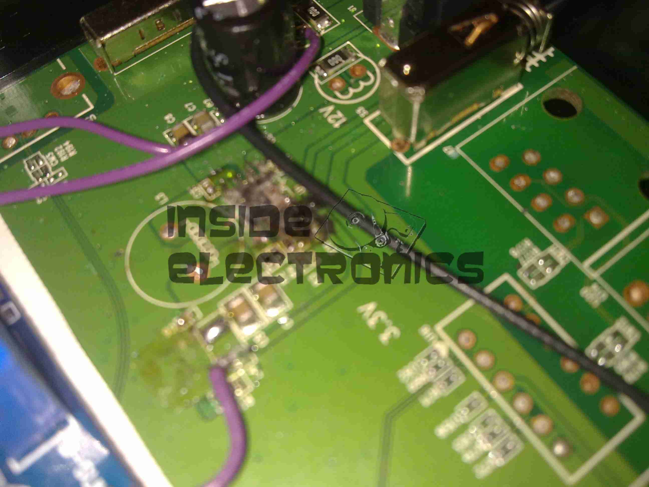
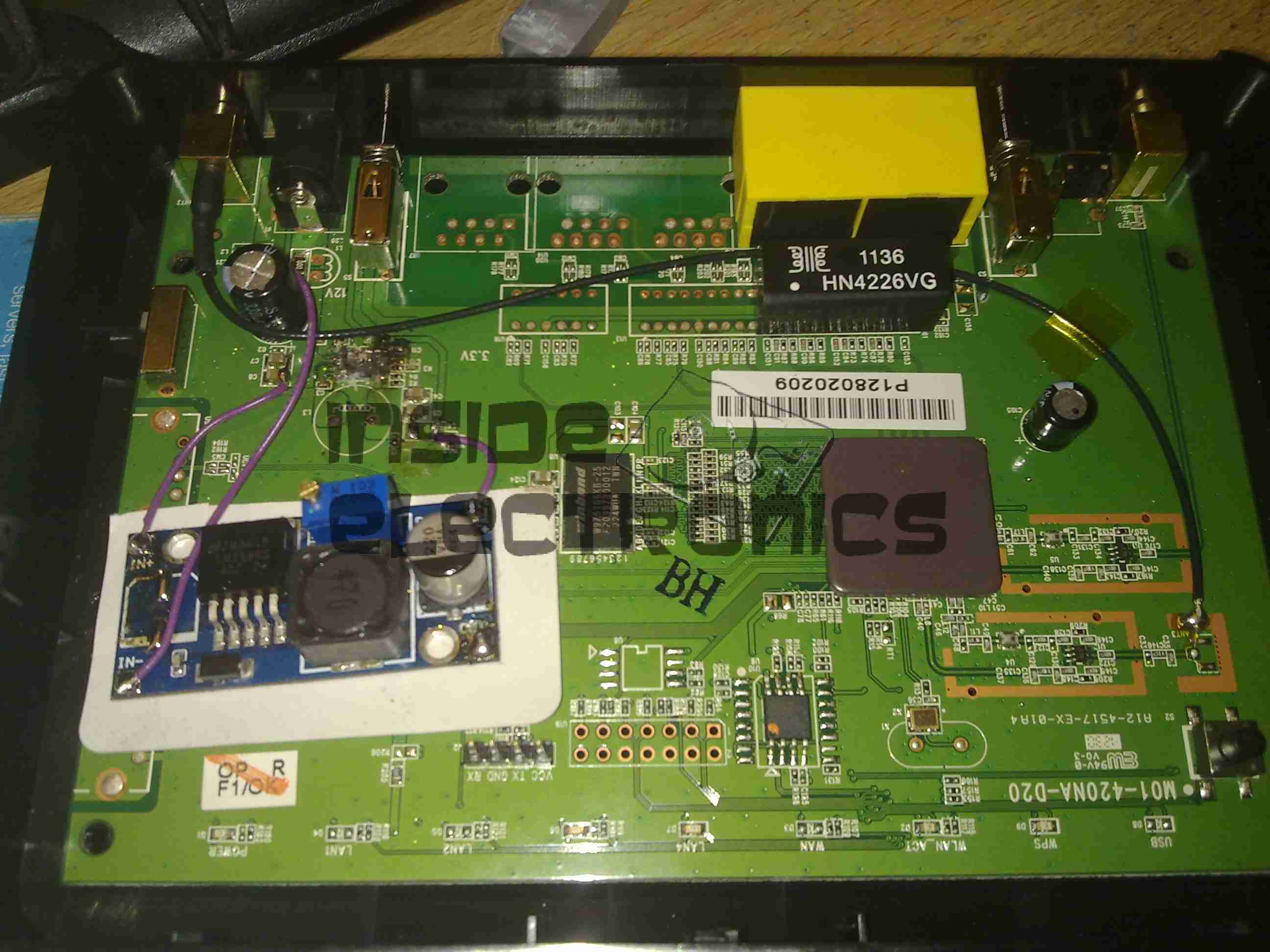
Here’s the mainboard power connector, with it’s silkscreen labelling on the pins. (Very useful). As can be seen here, there’s at least 5 regulators, of both switching & linear types here, generating both positive & negative rails.


More to come when I have some components!

73s for now 🙂

Posted on Leave a comment

Samsung ETA-U90UWE Adaptor Failure

Here’s an odd & sudden failure, the power adaptor for a Samsung device. It’s been working for months & on being plugged into the mains today the magic blue smoke escaped.

Samsung Charger
Samsung Charger

It’s one of their 2A models, for charging bigger devices like tablets.

Flash Burn
Flash Burn

Strangely for one of these chargers, no glue is used to hold it together – just clips. This made disassembly for inspection much easier. Evidence of a rather violent component failure is visible inside the back casing.

PCB
PCB

Here’s the charger PCB removed from the casing. As to be expected from Samsung, it’s a high quality unit, with all the features of a well designed SMPS.

PCB Reverse
PCB Reverse

However, on turning the board over, the blown component is easily visible. It’s the main SMPS controller IC, with a massive hole blown in the top. The on board fuse has also blown open, but it obviously didn’t operate fast enough to save the circuit from further damage!


Posted on Leave a comment

Chinese 12v 10A Power Brick Analysis

I recently ordered a PSU to run one of the TVs I converted to 12v operation, and being an older TV, it’s a fairly heavy load at 6.5A. eBay to the rescue again, with a cheap 10A rated supply.

Power Brick
Power Brick

Like all similar supplies these days, it’s a SMPS unit, and feels suspiciously light for it’s power rating.

Cover Removed
Cover Removed

Luckily this one is easy to get into, no ultrasonic welding on the case, just clips. Here’s the top cover removed, big alloy plate between the heatsinks.

PCB
PCB

The top heatsink plate was glued to the top of the transformer with silicone, some gentle prying released it. From the top, things don’t look too bad. There’s some filtering on the mains input & it’s even fused!

Primary Side
Primary Side

Here’s a closeup of the primary side of the PSU, the main DC bus capacitor is a Nichicon one, but it’s clearly been recovered from another device, look at the different glue on the end!
it’s also flapping about in the breeze, the squirt of silicone they’ve put on does nothing to stop movement.
Also here is the mains input fuse, filter capacitor & common mode choke. At least there is some filtering!

The main control IC is a UC3843B High Performance Current Mode PWM Controller, operating at a switching frequency of 250kHz.
The main switching transistor is visible at the bottom left corner, attached to the heatsink.

Secondary Side
Secondary Side

Here’s the secondary side of the supply. The transformer itself is OK, nice heavy windings on the output to suit the high current.
It’s using proper opto-isolated feedback for voltage regulation, with a TL431 reference IC.
The output diodes are attached to the heatsink at the top of the photo, I couldn’t read any numbers on those parts.

The output filter capacitors are low quality, only time will tell if they survive. I’ll put the supply under full load & see what the temperature rise is inside the casing.

PCB Bottom
PCB Bottom

On the bottom of the PCB things get a little more dire. There isn’t really much of an isolation gap between the primary & secondary sides, and there’s a track joining the output negative with mains earth, which gets to within 2mm of the live mains input!

As with all these cheapo supplies, there’s good points & bad points, I will update when I’ve had a chance to put the supply under full load for a while & see if it explodes!


Posted on 3 Comments

Evolis Dualys3 Card Printer Teardown

I recently dug out my other card printer to fit it with a 12v regulator, (it’s 24v at the moment), and figured I’d do a teardown post while I had the thing in bits.

This is a less industrial unit than my Zebra P330i, but unlike the Zebra, it has automatic duplexing, it doesn’t have Ethernet connectivity though.

Unlike domestic printers, which are built down to a price, these machines are very much built up to a spec, and feature some very high quality components.

Naked Printer
Naked Printer

Here’s the mechanism with the cowling removed. This is the main drive side of the printer, with the main drive stepper at left, ribbon take-up spool motor lower right, and the duplex module stepper motors at far right.

Main Motor Drive
Main Motor Drive

The main drive motor runs the various rollers in the card path through a pair of synchronous belts, shown here.

Main Stepper
Main Stepper

The stepper itself is a quality ball-bearing Sanyo Denki bipolar motor.

Main Stepper Driver
Main Stepper Driver

Electrical drive is provided to the stepper with a L6258EX DMOS universal motor driver. This chip can also drive DC motors as well as steppers.

Ribbon Supply Spool
Ribbon Supply Spool

Here is the encoder geared onto the ribbon supply spool. This is used to monitor the speed the ribbon is moving relative to the card.

Printer Top
Printer Top

Here’s a top view through the printer, the blue roller on the left cleans the card as it’s pulled from the feeder, the gold coloured spool to it’s right is the ribbon supply reel. The cooling fan on the right serves to stop the print head overheating during heavy use.

Spool Take Up Motor
Spool Take Up Motor

The spool take-up reel is powered by another very high quality motor, a Buhler DC gearmotor. These printers are very heavily over engineered!
This motor drives the spool through an O-Ring belt, before the gear above. This allows the drive to slip in the event the ribbon jams, preventing it from breaking.

Duplex Unit Stepper Drivers

The pair of steppers that operate the duplexing unit are driven by a separate board, with a pair of L6219DS bipolar stepper driver ICs. There are also a couple of opto-sensors on this board for the output hopper.


Main Control PCB
Main Control PCB

All the mechanisms of the printer are controlled from this main PCB, which handles all logic & power supply functions. Sections on the board are unpopulated, these would be for the Ethernet interface, smart card programming & magstripe programming.

Main CPU
Main CPU

The brains of the operation is this ColdFire MCF5208CVM166 32-bit microprocessor. It features 16KB of RAM, 8KB of cache, DMA controller, 3 UARTs, SPI, 10/100M Ethernet and low power management. This is a fairly powerful processor, running at 166MHz.
It’s paired with an external 128Mbit SDRAM from Samsung, and a Spansion 8Mbit boot sector flash, for firmware storage.

USB Interface & Power Input

Here the USB interface IC is located. It’s a USBN9604 from Texas Instruments, this interfaces with the main CPU via serial.

Posted on Leave a comment

Lethal Chinese Mains Adaptors

With every piece of Chinese electronics I obtain, mainly Baofeng radios, they come with a Europlug-type power adaptor, and a universal plug adaptor for the mains.

The charger units aren’t too bad, there’s a fair amount of isolation between the primary & secondary, and even though they’re very simple & cheap, I can’t see any immediate safety problems with them.

The plug adaptors, however, are a different matter. These things are utterly lethal!

Baofeng PSU
Baofeng PSU

Here’s the inside of the PSU. It’s just a very simple SMPS, giving an output of 10v 500mA. The fuse is actually a fusible resistor.

PCB Reverse
PCB Reverse

Here’s the back of the PCB with the SMPS control IC. I can’t find any English datasheets for this part unfortunately.

Universal Travel Adaptor

Here’s the dangerous adaptor. There’s no safety shield, so the live parts are exposed.

Internals
Internals

Here’s the adaptor split apart. The output contacts are on the left, and rely just on pressure to make contact with the brass screws on the mains input pins to provide power.
This is a very poor way to get a connection, a dirty or worn contact here would create a lot of heat if any significant power is pulled through, and could quite possibly result in a fire.

Not surprisingly, I bin these things as soon as I open the box, and charge all my radios with a 12v charging system.

Posted on Leave a comment

Uniden UBC92XLT Teardown

One bit of my equipment that I’ve never looked into is my scanner, a handheld Uniden unit. I got this when Maplin Electronics had them on special offer a few years ago.

Uniden Scanner
Uniden Scanner

Here’s the scanner itself, roughly the same size as a usual HT.

Back Cover Removed
Back Cover Removed

Here the back cover has been removed, and the main RF board is visible at the top of the stack. Unfortunately the shielding cans are soldered on this unit, so no looking under there 🙁
On the right hand side of the board next to the antenna input is the main RF filter network, and it’s associated switching. The RF front end is under the shield closest to the front edge.

Controls & 3.3v Regulator

On the other side of the PCB is the Volume & Squelch potentiometers, along with a dedicated 3.3v switching supply. An NJM2360A High Precision DC/DC converter IC controls this one. A 3.3v test point is visible next to the regulator.

RF Board Reverse
RF Board Reverse

Here’s the backside of the RF board, some more interesting parts here. There’s a pair of NJM3404A Single Supply Dual Op-Amp ICs, and a TK10931V Dual AM/FM IF Discriminator IC. This is the one that does all the back-end radio functionality. The audio amplifier for the internal speaker & external headphone jack is also on this PCB, top left. A board-to-board interconnect links this radio board with the main control board underneath.

Control PCB Front
Control PCB Front

Here’s the front of the control PCB, nothing much to see here, just the LCD & membrane keypad contacts.

Control PCB Reverse
Control PCB Reverse

And here’s the reverse side of the control board. All the interesting bits are here. The main microcontroller is on the right, a Renesas M38D59GF, a fairly powerful MCU, with onboard LCD drive, A/D converter, serial interface, 60K of ROM & 2K of RAM. It’s 6.143MHz clock crystal is just below it.
The mating connector for the RF board is in the centre here.

There is also a Microchip 24LC168 16KB I²C EEPROM next to the main microcontroller. This is probably for storing user settings, frequencies, etc.

EEPROM
EEPROM

The rest of this board is dedicated to battery charging and power supply, in the centre is a dual switching controller, I can’t figure out the numbers on the tiny SOT23 components in here, but this is dealing with the DC 6v input & to the left of that is the circuitry for charging the NiMH cells included with the scanner.

PSU
PSU

The last bit of this PCB is a BU2092FV Serial In / Parallel Out 4 channel driver. Not sure what this one is doing, it might be doing some signal multiplexing for the RF board interface. Unfortunately the tracks from this IC are routed on the inner layers of the board so they can’t be traced out.

Posted on 1 Comment

Aritech VV602 Vault Vibration Sensor

Here’s a rather unique device for protecting safes & vaults from attack by thefts.

It’s an Aritech VV602 seismic detector, based on piezoelectric sensors. Not surprisingly, this unit is covered in tamper sensors as well. There are several different sensor types in use:

  • Piezoelectric vibration sensing
  • Thermal sensing
  • Magnetic sensing
  • Manual Tamper Switches
Sensor Unit
Sensor Unit

Above is the main unit, with the thermal sensor. This is just a thermal fuse, very commonly used in everything from room heaters to hairdryers. This one triggers at 84°C. The adjustment pot is also visible here.

Mounting Plate
Mounting Plate

Above is the magnetic mounting plate used to attach the device to the safe. These units are apparently mounted over the keyhole of the safe to protect the lock, so they need to be easily removable to access the safe. This is a very strong magnet & it isn’t possible to pull it from a metal object without triggering the sensor.

Piezo Sensor
Piezo Sensor

Above is the piezo vibration sensor, bonded to the backplate. When the unit receives vibration or shock, this transducer generates a voltage, which is fed to the control logic below.

Control Logic
Control Logic

Here’s the reverse of the main PCB with the control logic ICs. These are basic logic gates, with a couple of comparators. One of the tamper switches is in the bottom left corner.

Main PCB
Main PCB

Main PCB with the connection terminals. Another tamper switch is in the top left corner, the solid-state relay is under the shield, next to the magnetic tamper switch. (Reed switch).
Some adjustment is provided for sensitivity. I’ve not found much of a difference in sensitivity though when it’s set to different levels.

Reed Tamper
Reed Tamper

Magnetic reed switch tamper on the right. Main output solid-state relay on the left under the shield.

This unit was given to me after it apparently went faulty. But on applying power it seems to work fine. Must be those experts again 😉

Posted on 1 Comment

SainSmart Frequency Meter

Thanks to Lewis, M3HHY for lending me this one 🙂

Here’s a quick look at a Sainsmart frequency counter module. These are useful little gadgets, showing the locked frequency on a small LCD display.

It’s built around an ATMega328 microcontroller (µC), and an MB501L Prescaler IC. The circuit for this is very simple, and is easily traced out from the board.

Frequency Counter
Frequency Counter

Here’s the back of the board, with the µC on the left & the prescaler IC on the right. This uses a rather novel method for calibration, which is the trimmer capacitor next to the crystal. This trimmer varies the frequency of the µC’s oscillator, affecting the calibration.

Input protection is provided by a pair of 1N4148 diodes in inverse parallel. These will clamp the input to +/-1v.
The prescaler IC is set to 1/64 divide ratio. This means that for an input frequency of 433MHz, it will output a frequency of 6.765625MHz to the µC.

The software in the µC will then calculate the input frequency from this intermediate frequency. This is done because the ATMega controllers aren’t very cabable of measuring such high frequencies.

The calculated frequency is then displayed on the LCD. This is a standard HD44780 display module.

LCD
LCD

Power is provided by a 9v PP3 battery, which is then regulated down by a standard LM7805 linear regulator.

Readout
Readout

I’ve found it’s not very accurate at all at the lower frequencies, when I fed it 40MHz from a signal generator it displayed a frequency of around 74MHz. This is probably due to the prescaler & the software not being configured for such a low input. In the case for 40MHz input the scaled frequency would have been 625kHz.


Posted on Leave a comment

Wouxun KG-UV950P RF Connector Replacement

In my original review, I noted that this radio was supplied with a SO-259 socket for the antenna connection.
However I’m less than fond of these, due to their non-constant impedance, which can cause signal loss issues at VHF/UHF. Because of this, I’ve replaced it with a high quality N-type connector. These connectors are much better, as they are a constant 50Ω impedance, they’re weather resistant, and being rated to 11GHz, are more than sufficient for a radio that will only do up to 70cm.

RF Output Jack
RF Output Jack

Here can be seen the point where the connection is made to the PCB.
I’ve already replaced the socket in this photo. The pair of solder pads either side of the central RF point were soldered to wings on the back of the original SO-259. As there are a pair of screws, also connected to the ground plane, there have been no signal issues with just using the frame of the radio as the ground point. Shown below is the original socket, with the ground wings.

Original SO-259
Original SO-259

Finally, here is the back of the radio with it’s shiny new N connector.

New Connection
New Connection

Chassis mount connectors are pretty standard, so this new connector fits perfectly into the same recess of the original. Looks like factory fitted!

I am now standardising on N connectors for everything in my radio shack, next on the project list for conversion is the SWR meter I recently acquired.

Stay tuned for more!

Posted on Leave a comment

Wouxun KG-UV950P Teardown & Analysis

Following on from my review, here are some internal views & detail on the components used in this radio. Below is an overview of the main PCB with the top plate removed from the radio.

Cover Removed
Cover Removed
RF Final Amplifier Stage

Most visible are these MOSFETs, which are Mitsubishi RD70HVF1 VHF/UHF power devices.  Rated for a maximum of 75W output power at 12.5v (absolute maximum of 150W, these are used well within their power ratings. They are joined to the PCB with heavy soldering, with bypass caps tacked right on to the leads.

RF Pre Drivers
RF Pre Drivers

Here is the RF pre-driver stage, with intermediate transistors hidden under the small brass heatspreader.

Power Section
Power Section

In the top left corner of the radio, near the power input leads, is the power supply & audio amplifier section. Clearly visible are the pair of LA4425A 5W audio power amplifier ICs, these drive the speakers on the top of the radio. Either side of these parts are a 7809 & a 7805 – both linear regulators providing +9v & +5v logic supplies respectively. The large TO220 package device is a KIA378R08PI 3A LDO regulator with ON/OFF control, this one outputs +8v. Just visible in the top right corner are the sockets for the speaker connections.

DTMF Circuits
DTMF Circuits

Here are the two ICs for dealing with DTMF tones, they are HM9170 receivers.

Glue Logic
Glue Logic

In the corner next to the interface jack, there are some CD4066B Quad Bilateral switches. These make sense since the interface jack has more than a single purpose, these will switch signals depending on what is connected.

RF Section
RF Section

Here are visible the RF cans for the oscillators, the crystals visible next to the can at the top. The shields are soldered on, so no opening these unfortunately.
Also visible in this image is a CMX138A Audio Scrambler & Sub-Audio Signalling processor. This IC deals with the Voice Inversion Scrambling feature of the radio, & processes the incoming audio before being sent to the modulator.

Output Filter Network

Shown here is the RF output filter network, this radio uses relays for switching instead of PIN diodes, I imagine for cost reasons. The relay closest to the RF output socket has had a slight accident 🙂 This is slated to be replaced soon.

RF Output Jack
RF Output Jack

Finally, the RF output jack.

Audio Speakers
Audio Speakers

Here the speakers are shown, attached to the bottom of the top plate. They are both rated 8Ω 1W.

Posted on Leave a comment

Moonraker SWR270 SWR & Power Meter

Meter Front
Meter Front

As I’m building up my radio shack, I figured an SWR meter would be a handy addition to my arsenal. This is a cheap Moonraker brand meter, which also will measure RF power. Above the front of the meter is shown, with the moving coil meter movement on the left, calibration adjustment on the right & the forward/reverse power switch.

Meter Rear
Meter Rear

For connections, standard SO-259 jacks are provided. The casing is sturdy 1mm steel. This is good, considering it’ll probably take a beating in my portable radio bag.

Directional Coupler PCB

Here the cover is removed, showing some of the internals. The large PCB across the back is the directional coupler.

Directional Coupler Circuit

The SO-259 connectors are bridged with a transmission line, (the track covered in solder in the image below), while there are a pair of sense lines running alongside. This main line is electromagnetically coupled to the two smaller sense lines, which are terminated at one end with resistors, with diodes at the other to rectify the coupled signal.
The termination resistors are sized to match the impedance of the sense lines.
The diodes, having rectified the coupled RF, produce DC voltages representing the value of the forward & reverse RF power. These DC voltages are smoothed with the capacitors.

PCB Marking
PCB Marking

The PCB is dated 19-8-2011, so it’s a fairly old design.

Adjustments
Adjustments

Here is visible the back of the user calibration adjuster, with the factory calibration trimmer.

Meter Movement
Meter Movement

Back of the meter movement. This is a standard moving coil type. Nothing special.


This meter will soon be modified to accept connection of an external Arduino-based SWR & power meter, which I can calibrate individually for each band.
Stay tuned for that upcoming project.

Posted on Leave a comment

Another Viewfinder CRT

Here’s another viewfinder CRT, removed from a 1980’s vintage VHS camera I managed to get cheap from eBay.

This unit is very similar to the last one I posted about, although there are a few small differences in the control circuitry.

Viewfinder Schematic
Viewfinder Schematic – Click to Embiggen

Here’s the schematic, showing all the functional blocks of the viewfinder circuitry. An integrated viewfinder IC is used, which generates all the required scan waveforms for the CRT.
On the left is the input connector, with the power & video signals. Only pins 2 (GND), 3 (Composite video), & 4 (+8v) are needed here. Pin 1 outputs a horizontal sync signal for use elsewhere in the camera, while pin 5 fed the recording indicator LED.

To make connection easier,  I have rearranged the wires in the input connector to a more understandable colour scheme:

Input Connector
Input Connector

Red & Blue for power input, & a coax for the video. For the video GND connection, I have repurposed the Rec. LED input pin, putting a shorting link across where the LED would go to create a link to signal ground. Keeping this separate from the power GND connection reduces noise on the CRT.

Viewfinder CRT Assembly

Here’s the complete assembly liberated from it’s plastic enclosure.

PCB Closeup
PCB Closeup

Closeup of the control PCB. The 3 potentiometers control the CRT brightness, focus & vertical size.

M01KGG007WB CRT
M01KGG007WB CRT

The tiny CRT. Only ~60mm in length, with an 18mm screen size. This tube runs on +2294v final anode voltage. Much higher than I expected.

Electron Gun Closeup

The electron gun assembly, with the cathode, focus & final anode cups.

Phosphor Screen
Phosphor Screen

This screen is just a little bigger than a UK 5p piece! A marvel of precision engineering.


Posted on 2 Comments

Active Ultracapacitor Balancing

Here’s another active balancing circuit for large ultracapacitor banks, this one is designed for a series string of 6, at 2.5v per capacitor.

Based on the design here, I have transcribed the circuit into Eagle & designed a PCB layout.

Ultracap Balancer Circuit
Ultracap Balancer Circuit – Click to Embiggen

As can be seen from the circuit diagram above, this is just 6 copies of the circuit from the above link, with screw terminals to attach to the capacitor string.

Ultracap Balancer PCB

And here’s the PCB. the MOSFETs & OpAmps are very small SMT parts, so require a steady hand in soldering. This board can easily be etched by hand as there’s only 3 links on the top side. No need for a double sided PCB.

As always, the Eagle project files & my Eagle library collection are available below:


Posted on 7 Comments

3″ CRT Composite Monitor

CRT Module

I recently managed to score a 3″ B&W portable TV on eBay, a Panasonic TR-3000G. As these old units are now useless, thanks to the switch off of analogue TV signalling, I figured I could find a composite signal internally & drive the CRT with an external source.

Panasonic TR-3000G
Panasonic TR-3000G

Here’s the TV in it’s native state. Running from 9v DC, or 6 D size cells. I’m guessing from somewhere around the 1970’s. Here is the CRT & associated drive circuitry, removed from the casing:

CRT Module
CRT Module

After dissecting the loom wiring between the CRT board & the RF/tuner board, I figured out I had to short out Pins 1,2 & 5 on the H header to get the CRT to operate straight from the power switch. This board also generates the required voltages & signals to drive the RF tuner section. I have removed the loom from this, as the PCB operates fine without. It doesn’t seem to be fussy about power input either: it’s specified at 9v, but seems to operate fine between 7.5v & 14.5v DC without issue.

Video Connections
Video Connections

Tracing the wiring from the tuner PCB revealed a length of coax snaking off to the section marked Video/Sync. I successfully found the composite input!

Running OSMC
Running OSMC

A quick bit of wiring to a Raspberry Pi, & we have stable video! For such an old unit, the picture quality is brilliant, very sharp focus.

Matsushita 85VB4 CRT

Closeup of the CRT itself. I haven’t been able to find much data on this unit, but I’m guessing it’s similar to many commercial viewfinder CRTs.

Electron Gun Closeup

Amazingly, there isn’t a single IC in the video circuitry, it’s all discrete components. This probably accounts for the large overall size of the control PCB. Viewfinder CRTs from a few years later on are usually driven with a single IC & a few passives that provide all the same functions.  

Posted on Leave a comment

uRadMonitor – Node Online!

It’s official. I’m now part of the uRadMonitor network, & assisting in some of the current issues with networking some people (including myself) have been having.

It seems that the uRadMonitor isn’t sending out technically-valid DHCP requests, here is what Wireshark thinks of the DHCP on my production network hardware setup:

WireShark Screencap
WireShark Screencap

As can be seen, the monitor unit is sending a DHCP request of 319 bytes, where a standard length DHCP Request packet should be ~324 bytes, as can be seen on the below screen capture.

Valid DHCP
Valid DHCP

This valid one was generated from the same SPI Ethernet module as the monitor, (Microchip ENC28J60) connected to an Arduino. Standard example code from the EtherCard library was used to set up the DHCP. The MAC address of the monitor was also cloned to this setup to rule out the possibility of that being the root cause.

My deductive reasoning in this case points to the firmware on the monitor being at fault, rather than the SPI ethernet hardware, or my network hardware. Radu over at uRadMonitor is looking into the firmware being at fault.

Strangely, most routers don’t seem to have an issue with the monitor, as connecting another router on a separate subnet works fine, and Wireshark doesn’t even complain about an invalid DHCP packet, although it’s exactly the same.

Working DHCP
Working DHCP

As the firmware for the devices isn’t currently available for me to pick apart & see if I can find the fault, it’s up to Radu to get this fixed at the moment.

Now, for a µTeardown:

uRadMonitor
uRadMonitor

Here is the monitor, a small aluminium box, with power & network.

PCB
PCB

Removing 4 screws in the end plate reveals the PCB, with the Geiger-Mueller tube along the top edge. My personal serial number is also on the PCB.
The ethernet module is on the right, with the DC barrel jack.

PCB Bottom
PCB Bottom

Here is the bottom of the PCB, with the control MCU & the tiny high voltage inverter for the Geiger tube.

Control Electronics
Control Electronics

A Closeup of the main MCU, an ATMega328p

Logo
Logo

PCB Logo. Very artsy 😉

Posted on Leave a comment

Quantum LTO2 CL1001 Tape Drive Teardown

Drive Top
Drive Top

I have recently begun to create an archive of all my personal data, and since LTO2 tape drives offer significant capacity (200GB/400GB) per tape, longevity is very high (up to 30 years in archive), & relatively low cost, this is the technology I’ve chosen to use for my long term archiving needs.

Unfortunately, this drive was DOA, due to being dropped in shipping. This drop broke the SCSI LVD connector on the back of the unit, & bent the frame, as can be seen below.

Broken SCSI
Broken SCSI

As this drive is unusable, it made for a good teardown candidate.

Cover Removed
Cover Removed

Here the top cover of the drive has been removed, showing the top of the main logic PCB. The large silver IC in the top corner is the main CPU for the drive. It’s a custom part, but it does have an ARM core.

The two Hitachi ICs are the R/W head interface chipset, while the smaller LSI IC is the SCSI controller.
The tape transport & loading mech can be seen in the lower half of the picture.

Main Logic
Main Logic

Close up of the main logic.

Tape Spool
Tape Spool

Here the main logic PCB has been removed, showing the tape take up spool. The data cartridges have only one spool to make the size smaller. When the tape is loaded, the drive grabs onto the leader pin at the end of the tape & feeds it onto this spool.
The head assembly is just above the spool.

Bottom Plate Removed

Bottom of the drive with the cover plate removed. Here the spindle drive motors are visible, both brushless 3-Phase units. Both of these motors are driven by a single controller IC on the other side of the lower logic PCB.

Head Drive Motor
Head Drive Motor

The head is moved up & down the face of the tape by this stepper motor for coarse control, while fine control is provided by a voice coil assembly buried inside the head mount.

Tape Head Assembly
Tape Head Assembly

The face of the tape R/W head. This unit contains 2 sets of 8 heads, one of which writes to the tape, the other then reads the written data back right after to verify integrity.

Cartridge Load Motor

The tape cartridge loading motor. I originally thought that this was a standard brushed motor, but it has a ribbon cable emerging, this must be some sort of brushless arrangement.

A replacement drive is on the way, I shall be documenting some more of my archiving efforts & system setup once that unit arrives.

Posted on Leave a comment

ZyXel WAP3205 Repair

Here is a ZyXel WAP3205 WiFi Access Point that has suffered a reverse polarity event, due to an incorrect power supply being used with the unit.

ZyXEL WAP3205
ZyXEL WAP3205

While most electronic gadgets are protected against reverse polarity with a blocking diode, this unit certainly wasn’t. Applying +12v DC the wrong way round resulted in this:

Blown Switchmode IC
Blown Switchmode IC (Fuzzy Focus)

That is the remains of the 3.3v regulator IC, blown to smithereens & it even attempted an arson attack. Luckily this was the only damaged component, & I was able to repair the unit by replacing the switching IC with a standalone regulator. (Replacing the IC would have been preferable, if there was anything left of it to obtain a part number from).

I scraped away the pins of the IC to clear the short on the input supply, removed the switching inductor, & tacked on an adjustable regulator module set to 3.3v. Luckily the voltage of the supply is handily marked on the PCB next to the circuit.

Replacement PSU
Replacement PSU

Replacement SMPS in place on top of the PCB. The output of the supply is connected to one of the pads of L4 (on my unit just an 0 ohm link), the +12v input is connected to the + rail side of C8 & C7 & the final ground connection is hooked in to the back of the barrel jack.

After this replacement, the unit booted straight up as if nothing had happened. All the logic is undamaged!

Makerplate
Makerplate
Posted on Leave a comment

AD9850 VFO Board

Continuing from my previous post where I published an Eagle design layout for AD7C‘s Arduino powered VFO, here is a completed board.

I have made some alterations to the design since posting, which are reflected in the artwork download in that post, mainly due to Eagle having a slight psychotic episode making me ground one of the display control signals!

AD9850 VFO
AD9850 VFO

The amplifier section is unpopulated & bypassed as I was getting some bad distortion effects from that section, some more work is needed there.
The Arduino Pro Mini is situated under the display, and the 5v rail is provided by the LM7805 on the lower left corner.

Current draw at 12v input is 150mA, for a power of 1.8W total. About 1W of this is dissipated in the LM7805 regulator, so I have also done a layout with an LM2574 Switching Regulator.
The SMPS version should draw a lot let power, as less is being dissipated in the power supply, but this version is more complex.

DDS VFO-SMPS
DDS VFO-SMPS

Here the SMPS circuit can be seen on the left hand side of the board, completely replacing the linear regulator.
I have not yet built this design, so I don’t know what kind of effect this will have on the output signal, versus the linear regulator. I have a feeling that the switching frequency of the LM2574 (52kHz) might produce some interference on the output of the DDS module. However I have designed this section to the standards in the datasheet, so this should be minimal.

Nevertheless this version is included in the Downloads section at the bottom of this post.

The output coupled through a 100nF capacitor is very clean, as can be seen below, outputting a 1kHz signal. Oscilloscope scale is 0.5ms/div & 1V/div.

VFO Output
VFO Output (Mucky ‘Scope)
Scope Connected
Scope Connected


Thanks again to Rich over at AD7C for the very useful tool design!

Linked below is the Eagle design files for this project, along with my libraries used to create it.

[download id=”5571″]

[download id=”5573″]

[download id=”5575″]

Posted on 4 Comments

AD9850 DDS VFO PCB & Schematic Layout

I recently came across a design for an Arduino controlled AD9850 DDS module, created by AD7C, so I figured I would release my Eagle CAD design for the PCB here.

It is a mainly single-sided layout, only a few links on the top side are needed so this is easy to etch with the toner transfer method.

My version uses an Arduino Pro Mini, as the modular format is much easier to work with than a bare ATMega 328.

RF output is via a SMA connector & has a built in amplifier to compensate for the low level generated by the DDS Module.

DDS VFO
DDS VFO

Version 2 Update: Added reverse polarity protection, added power indicator LED, beefed up tracks around the DC Jack.
[download id=”5571″]

Posted on Leave a comment

Water Management System PCB Revisions

OK, a few revisions have been made to the water management PCB, mainly to reduce the possibility of the brushed DC motors in the water pumps from causing the MCU to crash, with the other changes to the I/O connector positioning & finally upgrading the reverse blocking diode to a 10A capable version rather than 5A.

Water Management PCB

Thanks to Mayhew Labs with the WebGerber image generator for the render.

Posted on Leave a comment

Marine Potable Water Management System

LCD Panel
LCD Panel

Having two separate water tanks on nb Tanya Louise, with individual pumps, meant that monitoring water levels in tanks & keeping them topped up without emptying & having to reprime pumps every time was a hassle.
To this end I have designed & built this device, to monitor water usage from the individual tanks & automatically switch over when the tank in use nears empty, alerting the user in the process so the empty tanks can be refilled.

Based around an ATMega328, the unit reads a pair of sensors, fitted into the suction line of each pump from the tanks. The calculated flow is displayed on the 20×4 LCD, & logged to EEPROM, in case of power failure.

Water Flow Sensor
Water Flow Sensor

When the tank in use reaches a preset number of litres flowed, (currently hardcoded, but user input will be implemented soon), the pump is disabled & the other tank pump is enabled. This is also indicated on the display by the arrow to the left of the flow register. Tank switching is alerted by the built in beeper.
It is also possible to manually select a tank to use, & disable automatic operation.
Resetting the individual tank registers is done by a pair of pushbuttons, the total flow register is non-resettable, unless a hard reset is performed to clear the onboard EEPROM.

Main PCB
Main PCB

View of the main PCB is above, with the central Arduino Pro Mini module hosting the backend code. 12-24v power input, sensor input & 5v sensor power output is on the connectors on the left, while the pair of pump outputs is on the bottom right, switched by a pair of IRFZ44N logic-level MOSFETS. Onboard 5v power for the logic is provided by the LM7805 top right.

Code & PCB design is still under development, but I will most likely post the design files & Arduino sketch once some more polishing has been done.

Posted on Leave a comment

LM386 Stereo Audio Amplifier

The quickest project from inception to working PCB yet:

From inception to a working PCB took only 4 hours!

LM386 Amplifier
LM386 Amplifier

This is a miniature stereo audio amplifier, 0.5W per channel, that can be run from any voltage between 4-12v DC.

As usual, all the Eagle project files are available for download below & kits/bare PCBs will be available for sale for those that cannot etch boards.

In Operation
In Operation

Here is the circuit driving a pair of 3W 8Ω speakers from a line level audio source. The gain of this circuit is set at 50 with the components specified.


Schematic
Schematic

As can be seen from the schematic, this is a pair of single LM386 ICs for each channel.

Gain can be set by altering R3 & R4

[download id=”5566″]

Buy Kits Here £9.50:
[wp_cart_button name=”LM386 Stereo Audio Amplifier Kit” price=”9.50″]

Buy bare PCBs here £5:
[wp_cart_button name=”LM386 Stereo Audio Amplifier PCB” price=”5″]

PCBs are etched on FR4 laminate with 8oz copper with top component silkscreen.

Posted on Leave a comment

555 Flyback Driver

Flyback Secondary Waveform
Board Layout
Board Layout

Here is a simple 555 timer based flyback transformer driver, with the PCB designed by myself for some HV experiments. Above is the Eagle CAD board layout.

The 555 timer is in astable mode, generating a frequency from about 22kHz to 55kHz, depending on the position of the potentiometer. The variable frequency is to allow the circuit to be tuned to the resonant frequency of the flyback transformer in use.

This is switched through a pair of buffer transistors into a large STW45NM60 MOSFET, rated at 650v 45A.

Input power is 15-30v DC, as the oscillator circuit is fed from an independent LM7812 linear supply.

Provision is also made on the PCB for attaching a 12v fan to cool the MOSFET & linear regulator.

Initial Board
Initial Board

Board initially built, with the heatsink on the linear regulator fitted. I used a panel mount potentiometer in this case as I had no multiturn 47K pots in stock.

PCB Traces
PCB Traces

Bottom of the PCB. The main current carrying traces have been bulked up with copper wire to help carry the potentially high currents on the MOSFET while driving a large transformer.
This board was etched using the no-peel toner transfer method, using parchement paper as the transfer medium.

MOSFET Heatsinked
MOSFET Heatsinked

Main MOSFET now fitted with a surplus heatsink from an old switchmode power supply. A Fan could be fitted to the top of this sink to cope with higher power levels.

Gate Drive Waveform
Gate Drive Waveform

This is the gate drive waveform while a transformer is connected, the primary is causing some ringing on the oscillator. The waveform without an attached load is a much cleaner square wave.

Flyback Secondary Waveform

I obtained a waveform of the flyback secondary output by capacitively coupling the oscilloscope probe through the insulation of the HT wire. The pulses of HV can be seen with the decaying ringing of the transformer between cycles.

Corona Discharge
Corona Discharge
Arc Discharge
Arc Discharge

Corona & arc discharges at 12v input voltage.

Download the Eagle schematic files here: [download id=”5561″]

Posted on Leave a comment

Rio LAHS4 Salon Laser Hair Remover

Unit Overview
Unit Overview

Here is a home laser hair removal unit, a Rio LAHS4. Shown above is the system overview, with the laser wand & the user controls.

Main PCB Top
Main PCB Top

Main base unit popped open reveals the main PCB, with the central processor, a PIC16F628A.

Main PCB Bottom
Main PCB Bottom

Other side of the PCB is mainly populated with power supply & filtering for the logic sections.

Wand PCB
Wand PCB

Cracking open the laser wand reveals a stacked pair of PCBs, a main laser controller & the capacitive sensor PCB. This capacitive sensor connects to a pair of pins on the laser head & prevents operation if the unit is not held firmly against the skin.

Diode Module
Diode Module

Front of the laser diode module with the movable lens, on a pair of voice coil actuators. Very similar to the lens positioner used in any CD/DVD player pickup assembly.
The diode in this unit is an 808nm chip, with power in the 300-600mW range most likely.

Diode Module Rear
Diode Module Rear

Rear of the diode module, with the connections to the diode itself & the voice coil positioner for the lens.

Wand PCB Top
Wand PCB Top

Other side of the wand PCB, showing the capacitive sensor board on top of the main controller board. There is another CPU on the board here, which most likely communicates with the main processor in the base through a serial connection.


Posted on Leave a comment

Datakom DKG-171

Front
Front

Here is a teardown of the Datakom DKG-171 generator transfer controller. Here is the front of the unit, with the pictogram of the system, the indicator LEDs & the generator test button.


Rear
Rear

The rear of the unit features the connection points for the mains, generator & generator control I/O.

PCB Rear
PCB Rear

Rear of the PCB with the control relays. The two larger relays switch in the remote contactors to switch the mains supply over between the grid & the generator, while the smaller relay switches 12v power out to a terminal to automatically start the generator.

PCB Front
PCB Front

Front of the PCB with the control logic & main PIC microcontroller.